WO2020203507A1 - Monolithic semiconductor device and hybrid semiconductor device - Google Patents
Monolithic semiconductor device and hybrid semiconductor device Download PDFInfo
- Publication number
- WO2020203507A1 WO2020203507A1 PCT/JP2020/013168 JP2020013168W WO2020203507A1 WO 2020203507 A1 WO2020203507 A1 WO 2020203507A1 JP 2020013168 W JP2020013168 W JP 2020013168W WO 2020203507 A1 WO2020203507 A1 WO 2020203507A1
- Authority
- WO
- WIPO (PCT)
- Prior art keywords
- transistor
- semiconductor device
- region
- substrate
- semiconductor layer
- Prior art date
Links
- 239000004065 semiconductor Substances 0.000 title claims abstract description 449
- 239000000758 substrate Substances 0.000 claims abstract description 125
- 150000004767 nitrides Chemical class 0.000 claims abstract description 106
- 230000003321 amplification Effects 0.000 claims abstract description 23
- 238000003199 nucleic acid amplification method Methods 0.000 claims abstract description 23
- 230000005533 two-dimensional electron gas Effects 0.000 claims description 16
- 230000005540 biological transmission Effects 0.000 claims description 3
- 238000010586 diagram Methods 0.000 description 41
- 230000007423 decrease Effects 0.000 description 8
- 230000020169 heat generation Effects 0.000 description 8
- 230000000694 effects Effects 0.000 description 7
- 230000017525 heat dissipation Effects 0.000 description 7
- 230000001629 suppression Effects 0.000 description 7
- JMASRVWKEDWRBT-UHFFFAOYSA-N Gallium nitride Chemical compound [Ga]#N JMASRVWKEDWRBT-UHFFFAOYSA-N 0.000 description 6
- 229910002704 AlGaN Inorganic materials 0.000 description 5
- 229910002601 GaN Inorganic materials 0.000 description 5
- 238000004519 manufacturing process Methods 0.000 description 4
- 238000000926 separation method Methods 0.000 description 3
- 229920006395 saturated elastomer Polymers 0.000 description 2
- JBRZTFJDHDCESZ-UHFFFAOYSA-N AsGa Chemical compound [As]#[Ga] JBRZTFJDHDCESZ-UHFFFAOYSA-N 0.000 description 1
- 230000002238 attenuated effect Effects 0.000 description 1
- 239000000919 ceramic Substances 0.000 description 1
- 230000006866 deterioration Effects 0.000 description 1
- 238000010438 heat treatment Methods 0.000 description 1
- 238000009413 insulation Methods 0.000 description 1
- 230000007257 malfunction Effects 0.000 description 1
- 239000000463 material Substances 0.000 description 1
- 238000000034 method Methods 0.000 description 1
- 238000012986 modification Methods 0.000 description 1
- 230000004048 modification Effects 0.000 description 1
- 230000010363 phase shift Effects 0.000 description 1
- 230000000644 propagated effect Effects 0.000 description 1
- 239000011347 resin Substances 0.000 description 1
- 229920005989 resin Polymers 0.000 description 1
Images


Classifications
-
- H—ELECTRICITY
- H03—ELECTRONIC CIRCUITRY
- H03F—AMPLIFIERS
- H03F3/00—Amplifiers with only discharge tubes or only semiconductor devices as amplifying elements
- H03F3/189—High frequency amplifiers, e.g. radio frequency amplifiers
- H03F3/19—High frequency amplifiers, e.g. radio frequency amplifiers with semiconductor devices only
- H03F3/195—High frequency amplifiers, e.g. radio frequency amplifiers with semiconductor devices only in integrated circuits
-
- H—ELECTRICITY
- H01—ELECTRIC ELEMENTS
- H01L—SEMICONDUCTOR DEVICES NOT COVERED BY CLASS H10
- H01L21/00—Processes or apparatus adapted for the manufacture or treatment of semiconductor or solid state devices or of parts thereof
- H01L21/70—Manufacture or treatment of devices consisting of a plurality of solid state components formed in or on a common substrate or of parts thereof; Manufacture of integrated circuit devices or of parts thereof
- H01L21/77—Manufacture or treatment of devices consisting of a plurality of solid state components or integrated circuits formed in, or on, a common substrate
- H01L21/78—Manufacture or treatment of devices consisting of a plurality of solid state components or integrated circuits formed in, or on, a common substrate with subsequent division of the substrate into plural individual devices
- H01L21/82—Manufacture or treatment of devices consisting of a plurality of solid state components or integrated circuits formed in, or on, a common substrate with subsequent division of the substrate into plural individual devices to produce devices, e.g. integrated circuits, each consisting of a plurality of components
- H01L21/8252—Manufacture or treatment of devices consisting of a plurality of solid state components or integrated circuits formed in, or on, a common substrate with subsequent division of the substrate into plural individual devices to produce devices, e.g. integrated circuits, each consisting of a plurality of components the substrate being a semiconductor, using III-V technology
-
- H—ELECTRICITY
- H01—ELECTRIC ELEMENTS
- H01L—SEMICONDUCTOR DEVICES NOT COVERED BY CLASS H10
- H01L23/00—Details of semiconductor or other solid state devices
- H01L23/58—Structural electrical arrangements for semiconductor devices not otherwise provided for, e.g. in combination with batteries
- H01L23/64—Impedance arrangements
- H01L23/66—High-frequency adaptations
-
- H—ELECTRICITY
- H01—ELECTRIC ELEMENTS
- H01L—SEMICONDUCTOR DEVICES NOT COVERED BY CLASS H10
- H01L25/00—Assemblies consisting of a plurality of individual semiconductor or other solid state devices ; Multistep manufacturing processes thereof
- H01L25/16—Assemblies consisting of a plurality of individual semiconductor or other solid state devices ; Multistep manufacturing processes thereof the devices being of types provided for in two or more different main groups of groups H01L27/00 - H01L33/00, or in a single subclass of H10K, H10N, e.g. forming hybrid circuits
-
- H—ELECTRICITY
- H01—ELECTRIC ELEMENTS
- H01L—SEMICONDUCTOR DEVICES NOT COVERED BY CLASS H10
- H01L27/00—Devices consisting of a plurality of semiconductor or other solid-state components formed in or on a common substrate
- H01L27/02—Devices consisting of a plurality of semiconductor or other solid-state components formed in or on a common substrate including semiconductor components specially adapted for rectifying, oscillating, amplifying or switching and having at least one potential-jump barrier or surface barrier; including integrated passive circuit elements with at least one potential-jump barrier or surface barrier
- H01L27/04—Devices consisting of a plurality of semiconductor or other solid-state components formed in or on a common substrate including semiconductor components specially adapted for rectifying, oscillating, amplifying or switching and having at least one potential-jump barrier or surface barrier; including integrated passive circuit elements with at least one potential-jump barrier or surface barrier the substrate being a semiconductor body
- H01L27/06—Devices consisting of a plurality of semiconductor or other solid-state components formed in or on a common substrate including semiconductor components specially adapted for rectifying, oscillating, amplifying or switching and having at least one potential-jump barrier or surface barrier; including integrated passive circuit elements with at least one potential-jump barrier or surface barrier the substrate being a semiconductor body including a plurality of individual components in a non-repetitive configuration
- H01L27/0605—Devices consisting of a plurality of semiconductor or other solid-state components formed in or on a common substrate including semiconductor components specially adapted for rectifying, oscillating, amplifying or switching and having at least one potential-jump barrier or surface barrier; including integrated passive circuit elements with at least one potential-jump barrier or surface barrier the substrate being a semiconductor body including a plurality of individual components in a non-repetitive configuration integrated circuits made of compound material, e.g. AIIIBV
-
- H—ELECTRICITY
- H01—ELECTRIC ELEMENTS
- H01L—SEMICONDUCTOR DEVICES NOT COVERED BY CLASS H10
- H01L27/00—Devices consisting of a plurality of semiconductor or other solid-state components formed in or on a common substrate
- H01L27/02—Devices consisting of a plurality of semiconductor or other solid-state components formed in or on a common substrate including semiconductor components specially adapted for rectifying, oscillating, amplifying or switching and having at least one potential-jump barrier or surface barrier; including integrated passive circuit elements with at least one potential-jump barrier or surface barrier
- H01L27/04—Devices consisting of a plurality of semiconductor or other solid-state components formed in or on a common substrate including semiconductor components specially adapted for rectifying, oscillating, amplifying or switching and having at least one potential-jump barrier or surface barrier; including integrated passive circuit elements with at least one potential-jump barrier or surface barrier the substrate being a semiconductor body
- H01L27/06—Devices consisting of a plurality of semiconductor or other solid-state components formed in or on a common substrate including semiconductor components specially adapted for rectifying, oscillating, amplifying or switching and having at least one potential-jump barrier or surface barrier; including integrated passive circuit elements with at least one potential-jump barrier or surface barrier the substrate being a semiconductor body including a plurality of individual components in a non-repetitive configuration
- H01L27/0611—Devices consisting of a plurality of semiconductor or other solid-state components formed in or on a common substrate including semiconductor components specially adapted for rectifying, oscillating, amplifying or switching and having at least one potential-jump barrier or surface barrier; including integrated passive circuit elements with at least one potential-jump barrier or surface barrier the substrate being a semiconductor body including a plurality of individual components in a non-repetitive configuration integrated circuits having a two-dimensional layout of components without a common active region
- H01L27/0617—Devices consisting of a plurality of semiconductor or other solid-state components formed in or on a common substrate including semiconductor components specially adapted for rectifying, oscillating, amplifying or switching and having at least one potential-jump barrier or surface barrier; including integrated passive circuit elements with at least one potential-jump barrier or surface barrier the substrate being a semiconductor body including a plurality of individual components in a non-repetitive configuration integrated circuits having a two-dimensional layout of components without a common active region comprising components of the field-effect type
- H01L27/0629—Devices consisting of a plurality of semiconductor or other solid-state components formed in or on a common substrate including semiconductor components specially adapted for rectifying, oscillating, amplifying or switching and having at least one potential-jump barrier or surface barrier; including integrated passive circuit elements with at least one potential-jump barrier or surface barrier the substrate being a semiconductor body including a plurality of individual components in a non-repetitive configuration integrated circuits having a two-dimensional layout of components without a common active region comprising components of the field-effect type in combination with diodes, or resistors, or capacitors
-
- H—ELECTRICITY
- H03—ELECTRONIC CIRCUITRY
- H03F—AMPLIFIERS
- H03F1/00—Details of amplifiers with only discharge tubes, only semiconductor devices or only unspecified devices as amplifying elements
- H03F1/02—Modifications of amplifiers to raise the efficiency, e.g. gliding Class A stages, use of an auxiliary oscillation
- H03F1/0205—Modifications of amplifiers to raise the efficiency, e.g. gliding Class A stages, use of an auxiliary oscillation in transistor amplifiers
- H03F1/0288—Modifications of amplifiers to raise the efficiency, e.g. gliding Class A stages, use of an auxiliary oscillation in transistor amplifiers using a main and one or several auxiliary peaking amplifiers whereby the load is connected to the main amplifier using an impedance inverter, e.g. Doherty amplifiers
-
- H—ELECTRICITY
- H03—ELECTRONIC CIRCUITRY
- H03F—AMPLIFIERS
- H03F3/00—Amplifiers with only discharge tubes or only semiconductor devices as amplifying elements
- H03F3/20—Power amplifiers, e.g. Class B amplifiers, Class C amplifiers
- H03F3/21—Power amplifiers, e.g. Class B amplifiers, Class C amplifiers with semiconductor devices only
- H03F3/213—Power amplifiers, e.g. Class B amplifiers, Class C amplifiers with semiconductor devices only in integrated circuits
-
- H—ELECTRICITY
- H01—ELECTRIC ELEMENTS
- H01L—SEMICONDUCTOR DEVICES NOT COVERED BY CLASS H10
- H01L2223/00—Details relating to semiconductor or other solid state devices covered by the group H01L23/00
- H01L2223/58—Structural electrical arrangements for semiconductor devices not otherwise provided for
- H01L2223/64—Impedance arrangements
- H01L2223/66—High-frequency adaptations
- H01L2223/6644—Packaging aspects of high-frequency amplifiers
- H01L2223/665—Bias feed arrangements
-
- H—ELECTRICITY
- H01—ELECTRIC ELEMENTS
- H01L—SEMICONDUCTOR DEVICES NOT COVERED BY CLASS H10
- H01L2223/00—Details relating to semiconductor or other solid state devices covered by the group H01L23/00
- H01L2223/58—Structural electrical arrangements for semiconductor devices not otherwise provided for
- H01L2223/64—Impedance arrangements
- H01L2223/66—High-frequency adaptations
- H01L2223/6644—Packaging aspects of high-frequency amplifiers
- H01L2223/6655—Matching arrangements, e.g. arrangement of inductive and capacitive components
-
- H—ELECTRICITY
- H01—ELECTRIC ELEMENTS
- H01L—SEMICONDUCTOR DEVICES NOT COVERED BY CLASS H10
- H01L2223/00—Details relating to semiconductor or other solid state devices covered by the group H01L23/00
- H01L2223/58—Structural electrical arrangements for semiconductor devices not otherwise provided for
- H01L2223/64—Impedance arrangements
- H01L2223/66—High-frequency adaptations
- H01L2223/6661—High-frequency adaptations for passive devices
- H01L2223/6672—High-frequency adaptations for passive devices for integrated passive components, e.g. semiconductor device with passive components only
-
- H—ELECTRICITY
- H01—ELECTRIC ELEMENTS
- H01L—SEMICONDUCTOR DEVICES NOT COVERED BY CLASS H10
- H01L29/00—Semiconductor devices adapted for rectifying, amplifying, oscillating or switching, or capacitors or resistors with at least one potential-jump barrier or surface barrier, e.g. PN junction depletion layer or carrier concentration layer; Details of semiconductor bodies or of electrodes thereof ; Multistep manufacturing processes therefor
- H01L29/02—Semiconductor bodies ; Multistep manufacturing processes therefor
- H01L29/12—Semiconductor bodies ; Multistep manufacturing processes therefor characterised by the materials of which they are formed
- H01L29/20—Semiconductor bodies ; Multistep manufacturing processes therefor characterised by the materials of which they are formed including, apart from doping materials or other impurities, only AIIIBV compounds
- H01L29/2003—Nitride compounds
-
- H—ELECTRICITY
- H01—ELECTRIC ELEMENTS
- H01L—SEMICONDUCTOR DEVICES NOT COVERED BY CLASS H10
- H01L29/00—Semiconductor devices adapted for rectifying, amplifying, oscillating or switching, or capacitors or resistors with at least one potential-jump barrier or surface barrier, e.g. PN junction depletion layer or carrier concentration layer; Details of semiconductor bodies or of electrodes thereof ; Multistep manufacturing processes therefor
- H01L29/66—Types of semiconductor device ; Multistep manufacturing processes therefor
- H01L29/68—Types of semiconductor device ; Multistep manufacturing processes therefor controllable by only the electric current supplied, or only the electric potential applied, to an electrode which does not carry the current to be rectified, amplified or switched
- H01L29/76—Unipolar devices, e.g. field effect transistors
- H01L29/772—Field effect transistors
- H01L29/778—Field effect transistors with two-dimensional charge carrier gas channel, e.g. HEMT ; with two-dimensional charge-carrier layer formed at a heterojunction interface
- H01L29/7786—Field effect transistors with two-dimensional charge carrier gas channel, e.g. HEMT ; with two-dimensional charge-carrier layer formed at a heterojunction interface with direct single heterostructure, i.e. with wide bandgap layer formed on top of active layer, e.g. direct single heterostructure MIS-like HEMT
-
- H—ELECTRICITY
- H01—ELECTRIC ELEMENTS
- H01L—SEMICONDUCTOR DEVICES NOT COVERED BY CLASS H10
- H01L29/00—Semiconductor devices adapted for rectifying, amplifying, oscillating or switching, or capacitors or resistors with at least one potential-jump barrier or surface barrier, e.g. PN junction depletion layer or carrier concentration layer; Details of semiconductor bodies or of electrodes thereof ; Multistep manufacturing processes therefor
- H01L29/66—Types of semiconductor device ; Multistep manufacturing processes therefor
- H01L29/86—Types of semiconductor device ; Multistep manufacturing processes therefor controllable only by variation of the electric current supplied, or only the electric potential applied, to one or more of the electrodes carrying the current to be rectified, amplified, oscillated or switched
-
- H—ELECTRICITY
- H03—ELECTRONIC CIRCUITRY
- H03F—AMPLIFIERS
- H03F2200/00—Indexing scheme relating to amplifiers
- H03F2200/294—Indexing scheme relating to amplifiers the amplifier being a low noise amplifier [LNA]
-
- H—ELECTRICITY
- H03—ELECTRONIC CIRCUITRY
- H03F—AMPLIFIERS
- H03F2200/00—Indexing scheme relating to amplifiers
- H03F2200/447—Indexing scheme relating to amplifiers the amplifier being protected to temperature influence
-
- H—ELECTRICITY
- H03—ELECTRONIC CIRCUITRY
- H03F—AMPLIFIERS
- H03F2200/00—Indexing scheme relating to amplifiers
- H03F2200/451—Indexing scheme relating to amplifiers the amplifier being a radio frequency amplifier
Definitions
- This disclosure relates to monolithic semiconductor devices and hybrid semiconductor devices.
- a high electron mobility transistor (HEMT) using a nitride semiconductor such as gallium nitride (GaN) has a power density 10 times or more that of HEMT using a gallium arsenic semiconductor. Therefore, an amplifier circuit using HEMT using a nitride semiconductor as a high power device has been proposed (see, for example, Patent Document 1).
- an object of the present disclosure is to provide a monolithic semiconductor device and a hybrid semiconductor device including a transistor that can reduce the man-hours for individually adjusting the gate voltage.
- the monolithic semiconductor device is formed on a substrate, a first nitride semiconductor layer formed on the substrate, and the first nitride semiconductor layer.
- a HEMT type consisting of a second nitride semiconductor layer having a larger band gap than the first nitride semiconductor layer, the first nitride semiconductor layer, and the second nitride semiconductor layer formed on the substrate.
- a first transistor for power amplification and a HEMT type second transistor formed on the substrate and arranged outside the propagation path of a high-frequency signal input to the first transistor are included in the gate of the first transistor. It has a first bias circuit that gives a bias voltage.
- the hybrid semiconductor device includes the first monolithic semiconductor device and the second monolithic semiconductor device having a resistance element, unlike the first monolithic semiconductor device.
- the resistance element is used as a part of the first bias circuit.
- the monolithic semiconductor device and the hybrid semiconductor device according to the present disclosure reduce the man-hours for individually adjusting the gate voltage.
- FIG. 1 is a diagram illustrating a monolithic semiconductor device according to the first embodiment.
- FIG. 2 is a circuit diagram of the hybrid semiconductor device according to the second embodiment.
- FIG. 3 is a diagram illustrating a first resistor and a second resistor according to the third embodiment.
- FIG. 4 is a diagram illustrating a monolithic semiconductor device according to a fourth embodiment.
- FIG. 5 is a structural diagram of the first resistor and the second resistor according to the fifth embodiment.
- FIG. 6 is a diagram illustrating a first resistor and a second resistor according to the sixth embodiment.
- FIG. 7 is a diagram illustrating a monolithic semiconductor device according to the seventh embodiment.
- FIG. 8 is a diagram illustrating a monolithic semiconductor device according to the eighth embodiment.
- FIG. 1 is a diagram illustrating a monolithic semiconductor device according to the first embodiment.
- FIG. 2 is a circuit diagram of the hybrid semiconductor device according to the second embodiment.
- FIG. 3 is a diagram illustrating
- FIG. 9 is a diagram illustrating an enable control circuit according to the ninth embodiment.
- FIG. 10 is a plan layout view of the hybrid semiconductor device according to the tenth embodiment.
- FIG. 11 is a circuit diagram of the noise suppression circuit according to the eleventh embodiment.
- FIG. 12 is a circuit diagram of the noise suppression circuit according to the twelfth embodiment.
- FIG. 13 is a diagram illustrating a monolithic semiconductor device according to the thirteenth embodiment.
- FIG. 14 is a diagram illustrating a monolithic semiconductor device according to a fourteenth embodiment.
- FIG. 15 is a plan layout view of the monolithic semiconductor device according to the fifteenth embodiment.
- FIG. 16 is a plan layout view of the monolithic semiconductor device according to the sixteenth embodiment.
- FIG. 16 is a plan layout view of the monolithic semiconductor device according to the sixteenth embodiment.
- FIG. 17 is a plan layout view of the monolithic semiconductor device according to the seventeenth embodiment.
- FIG. 18 is a plan layout view of the monolithic semiconductor device according to the eighteenth embodiment.
- FIG. 19 is a plan layout view of the monolithic semiconductor device according to the nineteenth embodiment.
- FIG. 20 is a plan layout view of the hybrid semiconductor device according to the 20th embodiment.
- FIG. 21 is a plan layout view of the hybrid semiconductor device according to the twenty-first embodiment.
- FIG. 22 is a plan layout view of the hybrid semiconductor device according to the 22nd embodiment.
- FIG. 23 is a plan layout view of the hybrid semiconductor device according to the 23rd embodiment.
- FIG. 24 is a plan layout view of the hybrid semiconductor device according to the twenty-fourth embodiment.
- FIG. 25 is a plan layout view of the hybrid semiconductor device according to the 25th embodiment.
- FIG. 26 is a plan layout view of the hybrid semiconductor device according to the twenty-sixth embodiment.
- FIG. 27 is a plan layout view of the hybrid semiconductor device according to the 27th embodiment.
- FIG. 28 is a plan layout view of the hybrid semiconductor device according to the 28th embodiment.
- FIG. 29 is a plan layout view of the hybrid semiconductor device according to the 29th embodiment.
- FIG. 30 is a plan layout view of the monolithic semiconductor device according to the thirtieth embodiment.
- FIG. 31 is a plan layout view of the monolithic semiconductor device according to the 31st embodiment.
- FIG. 32 is a diagram illustrating a monolithic semiconductor device according to the 32nd embodiment.
- FIG. 33 is a diagram illustrating a monolithic semiconductor device according to the 33rd embodiment.
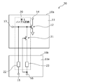
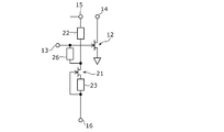
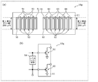
- FIG. 1 is a diagram illustrating a monolithic semiconductor device 10 according to the first embodiment. More specifically, FIG. 1A is a circuit diagram of the monolithic semiconductor device 10.
- FIG. 1B is a diagram showing a cross-sectional structure of the first transistor 12 and the second transistor 21 in FIG. 1A.
- the threshold voltage of the second transistor 21 (that is, the variation of the threshold voltage) is taken as the horizontal axis, and the drain current (broken line) of the second transistor 21 when there is no signal (that is, idle).
- the threshold voltage of the first transistor 12 (that is, the variation of the threshold voltage) is taken as the horizontal axis, and the drain current (solid line) of the first transistor 12 when there is no signal (that is, idle). It is a characteristic figure which shows the threshold voltage dependence of the 1st transistor 12 with the current) as a vertical axis. As a reference, FIG. 1D also includes the threshold voltage dependence (broken line) obtained when the gate bias of the first transistor 12 is fixed without connecting the first bias circuit 20. It is illustrated.
- the monolithic semiconductor device 10 is a one-chip semiconductor device, which is a semiconductor substrate 11, a HEMT type first transistor 12 formed on the substrate 11 for power amplification, and a HEMT type formed on the substrate 11. It includes a second transistor 21, and has a first bias circuit 20 that applies a bias voltage to the gate of the first transistor 12.
- the first bias circuit 20 is composed of a first resistor 22, a second transistor 21, and a second resistor 23 connected in series.
- the connection point between the first resistor 22 and the drain of the second transistor 21 corresponds to the bias voltage output node of the first bias circuit 20, and is connected to the gate of the first transistor 12.
- the second transistor 21 is arranged outside the propagation path of the high frequency signal input to the first transistor 12.
- One end of the second resistor 23 is connected to the source of the second transistor 21, and the other end is connected to the gate of the second transistor 21.
- the high-frequency signal propagation path is a path in which most of the high-frequency signal input to the gate terminal 13 is propagated.
- the monolithic semiconductor device 10 has a gate terminal 13 connected to the gate of the first transistor 12, a drain terminal 14 connected to the drain of the first transistor 12, and a first bias connected to one end of the first resistor 22.
- a terminal 15 and a second bias terminal 16 connected to one end of the second resistor 23 are provided.
- the source of the first transistor 12 is grounded. Further, a voltage higher than that of the second bias terminal 16 is applied to the first bias terminal 15.
- One of the first bias terminal 15 and the second bias terminal 16 may be grounded.
- a first nitride semiconductor layer 102 made of GaN or the like is formed on the substrate 11 made of Si or the like, and is above the first nitride semiconductor layer 102.
- a second nitride semiconductor layer 103 made of AlGaN or the like having a larger band gap than the first nitride semiconductor layer 102 is formed in the above, and SiN or the like is formed on the second nitride semiconductor layer 103.
- a drain electrode 110, a gate electrode 111, and a source electrode 112 separated by an insulating layer 106 are formed.
- a two-dimensional electron gas layer 107 is formed at the interface between the first nitride semiconductor layer 102 and the second nitride semiconductor layer 103.
- an element separation layer 104 for insulating the first nitride semiconductor layer 102 and the second nitride semiconductor layer 103 from other circuit elements is formed on the substrate 11.
- the gate electrode 111 is Schottky-bonded to the second nitride semiconductor layer 103, and the drain electrode 110 and the source electrode 112 are ohmic with the two-dimensional electron gas layer 107 that functions as a channel by being heat-treated or the like. You are connected.
- the first transistor 12 and the second transistor 21 are HEMT type transistors formed on the substrate 11 and composed of the first nitride semiconductor layer 102 and the second nitride semiconductor layer 103.
- a high-frequency signal is transmitted to the gate terminal 13 in a state where an appropriate bias voltage is applied to each of the first bias terminal 15 and the second bias terminal 16.
- power amplification is performed using the first transistor 12 as a high power device, and the output signal after power amplification is output from the drain terminal 14.
- the drain current of a transistor changes due to the difference between the threshold voltage and the gate bias, and when the gate bias is fixed, the drain current changes significantly due to the change in the threshold voltage due to manufacturing variations, for example.
- the drain current decreases as the threshold voltage increases.
- the threshold voltage of the first transistor 12 now varies to the higher side.
- the second transistor 21 formed on the same substrate 11 and having the same structure as the first transistor 12 also varies toward the higher threshold voltage. Since the constant current source circuit is composed of the second transistor 21 and the second resistor 23, the drain current (that is, idle current) of the second transistor 21 decreases as the threshold voltage of the second transistor 21 increases (that is, the idle current). In FIG. 1C), the amount of voltage drop generated by the drain current of the second transistor 21 and the first resistor 22 is reduced. As a result, the gate voltage of the first transistor 12 rises, so that the gate bias of the first transistor 12 rises as the threshold voltage of the first transistor 12 rises.
- the idle current can be kept within the permissible range even with a constant voltage source by the first bias circuit 20 that changes the gate voltage of the first transistor 12 according to the variation of the threshold voltage. Therefore, the number of steps to adjust the gate voltage individually is reduced.
- FIG. 2 is a circuit diagram of the hybrid semiconductor device 30 according to the second embodiment.
- the hybrid semiconductor device 30 basically has the same circuit configuration as the monolithic semiconductor device 10 according to the first embodiment, but is formed separately on two substrates 11 and 11a (that is, a two-chip semiconductor device). It differs from the first embodiment in that (consisting of).
- the hybrid semiconductor device 30 includes two substrates 11 and 11a, and has the first transistor 12, the second transistor 21, the first resistor 22, the second resistor 23, the gate terminal 13, and the drain terminal 14 as circuit elements. It includes a first bias terminal 15 and a second bias terminal 16. On top of these circuit elements, the first transistor 12, the second transistor 21, the gate terminal 13 and the drain terminal 14 are formed on the substrate 11, and the first resistor 22, the second resistor 23, the first bias terminal 15, and the first bias terminal 15 are formed. , The second bias terminal 16 is formed on the substrate 11a.
- the monolithic semiconductor device formed by using the substrate 11 can be called the first monolithic semiconductor device 10a, and the monolithic semiconductor device formed by using the substrate 11a can be called the second monolithic semiconductor device 10b.
- the hybrid semiconductor device 30 is composed of a first monolithic semiconductor device 10a and a second monolithic semiconductor device 10b.
- the first monolithic semiconductor device 10a and the second monolithic semiconductor device 10b are connected via a wire or a wiring pattern formed on a submount substrate (not shown).
- the hybrid semiconductor device 30 according to the present embodiment configured in this way, in addition to the effect of the first embodiment, the following effect due to the circuit being dispersed on the two substrates 11 and 11a is formed. Is played. That is, the signal amplification transistor such as the first transistor 12 may generate heat due to the operating current and heat other circuit elements.
- the signal amplification transistor such as the first transistor 12 may generate heat due to the operating current and heat other circuit elements.
- the first resistor 22 and the second resistor 23 are formed on the substrate 11a different from the first transistor 12, they are affected by the heat generated by the first transistor 12. Is reduced, and stable operation of the hybrid semiconductor device 30 is ensured.
- FIG. 3 is a diagram for explaining the first resistor 22 and the second resistor 23 according to the third embodiment. More specifically, FIG. 3A shows a planar layout of the first resistor 22 and the second resistor 23. FIG. 3B shows the drain current of the first transistor 12 according to the second embodiment including the first resistor 22 and the second resistor 23. In FIG. 3B, the horizontal axis represents the value (resistance ratio) obtained by dividing the resistance value of the first resistor 22 by the resistance value of the second resistor 23, and the vertical axis represents the drain current of the first transistor 12. Shown. In addition, in FIG. 3B, in addition to the range of values in the present embodiment, the range of values in the normal case as a reference (when the feature of the plane layout in the present embodiment is not provided) is also shown. ing.
- the first resistor 22 and the second resistor 23 are placed between the two first resistor 22 and the second resistor 23 in the plan view of the second monolithic semiconductor device 10b.
- the elements are adjacent to each other without sandwiching them, and are arranged so that the directions of the currents flowing through the respective resistance elements are the same.
- the gate voltage of the first transistor 12 changes and the drain current of the first transistor 12 changes.
- the first resistor 22 and the second resistor 23 are formed so as to have the same structure, the same width (the same length in the direction orthogonal to the current flow direction), and the same current direction. Therefore, the influence of manufacturing variation on the resistance ratios of the first resistor 22 and the second resistor 23 is reduced. As a result, as shown in FIG.
- the variation in the drain current of the first transistor 12 according to the second embodiment including the first resistor 22 and the second resistor 23 having such an identity is This is reduced as compared with the case (normal case) composed of the first resistor and the second resistor having no such identity.
- FIG. 4 is a diagram illustrating the monolithic semiconductor device 10c according to the fourth embodiment. More specifically, FIG. 4A shows a circuit diagram of the monolithic semiconductor device 10c. FIG. 4B shows the resistance value (horizontal axis) of the second resistor 23 with respect to the noise power (vertical axis) at the gate terminal of the first transistor 12 when noise is applied to the second bias terminal 16. Shows dependencies. In addition, in FIG. 4B, for reference, the noise power (broken line) in the normal case where the second resistor 23 does not exist (short-circuited) is also shown.
- the monolithic semiconductor device 10c biases the substrate 11, the HEMT type first transistor 12 for power amplification formed on the substrate 11, and the gate of the first transistor 12. It has a second bias circuit 20a that applies a voltage.
- the second bias circuit 20a includes a first resistor 22 and a second resistor 23 connected in series as at least two resistance elements.
- the bias voltage is a voltage divider voltage generated by the first resistor 22 and the second resistor 23.
- the first transistor 12 is a transistor composed of the first nitride semiconductor layer 102 and the second nitride semiconductor layer 103, as in the first embodiment.
- the gate bias of the first transistor 12 which is a signal amplification transistor, is applied from the outside, noise may be superimposed.
- the gate terminal of the first transistor 12 has a second resistor 23. Since it is connected to the outside of the substrate 11 via the substrate 11, noise from the outside is attenuated by the second resistor 23 and input to the gate terminal of the first transistor 12. As a result, as shown in FIG. 4B, the influence of noise from the outside is reduced as compared with the case where the second resistor 23 does not exist (short-circuited).
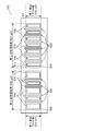
- FIG. 5 is a structural diagram of the first resistor 22 and the second resistor 23 according to the fifth embodiment. More specifically, FIG. 5A shows the planar layout of the first resistor 22 and the second resistor 23, and FIG. 5B shows the cross-sectional structure of FIG. 5A in the VV line. ..
- a first nitride semiconductor layer 102 composed of GaN or the like is formed on the substrate 11, and AlGaN or the like having a larger band gap than the first nitride semiconductor layer 102 is formed on the first nitride semiconductor layer 102.
- a second nitride semiconductor layer 103 composed of the above is formed, and a first electrode 113 and a second electrode 114 separated by an insulating layer 106 are formed on the second nitride semiconductor layer 103.
- a two-dimensional electron gas layer 107 is formed near the interface between the first nitride semiconductor layer 102 and the second nitride semiconductor layer 103.
- an element separation layer 104 for insulating the first nitride semiconductor layer 102 and the second nitride semiconductor layer 103 from other circuit elements is formed on the substrate 11.
- the first electrode 113 and the second electrode 114 are ohmic-connected to the two-dimensional electron gas layer 107 that functions as an electric resistance element by being subjected to heat treatment or the like, and are configured as both connection terminals of the electric resistance element. There is.
- the first resistor 22 and the second resistor 23 according to the present embodiment configured in this way have a characteristic that the resistance value increases at a high temperature because the two-dimensional electron gas layer functions as an electric resistance element. Therefore, the first resistor 22 and the second resistor 23 according to the present embodiment are used as resistance elements (first resistor 22 and second resistor 23) of the second bias circuit 20a in the monolithic semiconductor device 10c according to the fourth embodiment.
- the resistor By using the resistor, it becomes possible to integrate the resistor without adding a step, and the current flowing through the second bias circuit 20a at a high temperature is reduced.
- the two first resistance 22 and the second resistance 23 are both resistance elements having a two-dimensional electron gas layer as an electric resistance element, but only one of them is a two-dimensional electron gas. It is a resistance element having a layer as an electric resistance element, and other resistance elements may be ordinary resistance elements such as chip resistors.
- FIG. 6 is a diagram for explaining the first resistor 22 and the second resistor 23 according to the sixth embodiment. More specifically, FIG. 6 (a) shows a planar layout of the first resistor 22 and the second resistor 23, and FIG. 6 (b) includes such a first resistor 22 and a second resistor 23.
- the drain current of the first transistor 12 according to the fourth embodiment is shown.
- the horizontal axis represents the resistance value of the first resistor 22 divided by the resistance value of the second resistor 23 (resistor ratio), and the vertical axis represents the drain current of the first transistor 12. Shown.
- the range in the normal case as a reference when it does not have the characteristics of the plane layout in the present embodiment is also shown. ..
- the first resistor 22 and the second resistor 23 are other elements between the two first resistor 22 and the second resistor 23 in the plan view of the monolithic semiconductor device 10c. Are adjacent to each other without sandwiching them, and are arranged so that the current directions flowing through the respective resistance elements are the same.
- the gate voltage of the first transistor 12 changes and the drain current of the first transistor 12 changes.
- the first resistor 22 and the second resistor 23 are formed so as to have the same structure, the same width, and the same current direction, the resistance ratio of the first resistor 22 and the second resistor 23 The effect of manufacturing variation on is reduced.
- the variation in the drain current of the first transistor 12 according to the second embodiment including the first resistor 22 and the second resistor 23 having such an identity is found. This is reduced as compared with the case (normal case) composed of the first resistor and the second resistor having no such identity.
- FIG. 7 is a diagram illustrating the monolithic semiconductor device 10d according to the seventh embodiment. More specifically, FIG. 7A is a circuit diagram of the monolithic semiconductor device 10d.
- FIG. 7B the threshold voltage of the second transistor 21 (that is, the variation of the threshold voltage) is taken as the horizontal axis, and the drain current (broken line) of the second transistor 21 when there is no signal (that is, idle).
- FIG. 7B It is a characteristic diagram which shows the threshold voltage dependence of the 2nd transistor 21 with the left vertical axis
- the threshold voltage of the first transistor 12 (that is, the variation of the threshold voltage) is taken as the horizontal axis, and the drain current (solid line) of the first transistor 12 when there is no signal (that is, idle). It is a characteristic figure which shows the threshold voltage dependence of the 1st transistor 12 with the current) as a vertical axis.
- the monolithic semiconductor device 10d according to the present embodiment basically has the same circuit configuration as the monolithic semiconductor device 10 according to the first embodiment.
- the first resistor 22 and the second resistor 23 constituting the first bias circuit 20 are resistance elements having the two-dimensional electron gas layer described in the fifth embodiment as an electric resistance element, and are as described in the sixth embodiment.
- it differs from the first embodiment in that it is formed so as to have the same structure, the same width, and the same current direction, and is not limited to such a resistance element.
- the second transistor when the threshold voltage of the first transistor 12 varies to the higher side, the second transistor formed on the same substrate 11 with the same structure as the first transistor 12.
- the threshold voltage of 21 also varies to the higher side. Since the constant current source circuit is composed of the second transistor 21 and the second resistor 23, the drain current of the second transistor 21 decreases as the threshold voltage of the second transistor 21 increases, as in the first embodiment. ((B) in FIG. 7), the amount of voltage drop generated by the drain current of the second transistor 21 and the first resistor 22 is reduced. As a result, the gate voltage of the first transistor 12 rises, so that the gate bias of the first transistor 12 rises as the threshold voltage of the first transistor 12 rises.
- the idle current can be kept within the permissible range even with a constant voltage source by the first bias circuit 20 that changes the gate voltage of the first transistor 12 according to the variation of the threshold voltage. Therefore, the number of steps to adjust the gate voltage individually is reduced.
- first resistance 22 and the second resistance 23 constituting the first bias circuit 20 are resistance elements in which the two-dimensional electron gas layer functions as an electric resistance element, and have a characteristic that the resistance value increases at a high temperature. The current flowing through the first bias circuit 20 at high temperatures is reduced.
- the variation in the drain current of the first transistor 12 is compared with the case where the first resistor 12 does not have such an identity. It will be reduced.
- FIG. 8 is a diagram illustrating the monolithic semiconductor device 10e according to the eighth embodiment. More specifically, FIG. 8A is a circuit diagram of the monolithic semiconductor device 10e, and FIGS. 8B to 8D are examples of layouts of the first to third planes of the monolithic semiconductor device 10e, respectively. Shown.
- the monolithic semiconductor device 10e includes the first nitride semiconductor layer 102 and the first nitride semiconductor layer 102 formed on the substrate 11 in addition to the configuration of the monolithic semiconductor device 10 according to the first embodiment. It has a HEMT type third transistor 40 for power amplification composed of a second nitride semiconductor layer 103, and a third bias circuit 20b that applies a bias voltage to the gate of the third transistor 40.
- the third bias circuit 20b is composed of a third resistor 24 and a fourth resistor 25 connected in series.
- the connection point between the third resistor 24 and the fourth resistor 25 corresponds to the bias voltage output node of the third bias circuit 20b, and is connected to the gate of the third transistor 40.
- the third bias circuit 20b does not include a HEMT type transistor.
- a third bias terminal 43 connected to one end of the 24 and a fourth bias terminal 44 connected to one end of the fourth resistor 25 are provided.
- a voltage higher than that of the fourth bias terminal 44 is applied to the third bias terminal 43.
- One of the third bias terminal 43 and the fourth bias terminal 44 may be grounded.
- the monolithic semiconductor device 10e constitutes a Doherty amplifier circuit in which the first transistor 12 is a carrier amplifier and the third transistor 40 is a peak amplifier.
- the Doherty amplifier circuit has a configuration in which the outputs of a class B or class AB amplifier called a carrier amplifier that operates at all times and a class C amplifier called a peak amplifier that operates only at peak power are directly coupled, and the output level is relatively high. It is a high frequency amplifier that has good efficiency even in a low region.
- the distance between the adjacent gates is set to be twice or more the thickness of the substrate 11 (for example, 200 ⁇ m or more when the thickness of the substrate 11 is 100 ⁇ m). Further, in consideration of heat dissipation of the first transistor 12 (carrier amplifier), the shortest distance between the gate of the first transistor 12 (carrier amplifier) and the end of the substrate 11 is equal to or greater than the thickness of the substrate 11 (for example, the thickness of the substrate 11 is large). In the case of 100 ⁇ m, it is set to 100 ⁇ m or more).
- the first transistor 12 (carrier amplifier) and the third transistor 40 (peak amplifier) are comb-type (that is, multi-finger type) transistors.
- the first bias circuit 20 for the first transistor 12 is arranged directly below the first transistor 12 (carrier amplifier) in the planar layout, and the second transistor 21 constituting the first bias circuit 20 is the first. It is arranged near the center of the first transistor 12 (carrier amplifier) in the direction in which the fingers of the one transistor 12 (carrier amplifier) are lined up.
- the first transistor 12 carrier amplifier
- the second transistor 21 constituting the first bias circuit 20 are arranged close to each other, and the positions of these fingers in the line-up direction are the same. Characteristic difference is reduced.
- the shortest distance between the gate of the first transistor 12 (carrier amplifier) and the end of the substrate 11 is set in consideration of heat dissipation of the first transistor 12 (carrier amplifier).
- the thickness of the substrate 11 or more (for example, when the thickness of the substrate 11 is 100 ⁇ m, 100 ⁇ m or more) is set.
- the first bias circuit 20 for the first transistor 12 (carrier amplifier) is arranged between the first transistor 12 (carrier amplifier) and the third transistor 40 (peak amplifier), and the first bias circuit 20
- the second transistor 21 constituting the first transistor 12 (carrier amplifier) is arranged in an extended range in the direction in which the fingers of the first transistor 12 (carrier amplifier) are lined up.
- the gate distance between the first transistor 12 (carrier amplifier) and the second transistor 21 may be close to 50 ⁇ m or less. Further, the bias resistors (third resistor 24 and fourth resistor 25) for the third transistor 40 (peak amplifier) may be arranged close to the second transistor 21 at 50 ⁇ m or less.
- first bias circuit 20 and third bias circuit 20b By arranging two bias circuits (first bias circuit 20 and third bias circuit 20b) in the space between the first transistor 12 (carrier amplifier) and the third transistor 40 (peak amplifier), the first transistor The distance between the gates where the 12 (carrier amplifier) and the third transistor 40 (peak amplifier) are closest to each other is secured at least twice the thickness of the substrate 11, and the first transistor 12 (carrier amplifier) and the third transistor 40 (peak) are secured. Thermal and signal interference with the amplifier) is suppressed.
- the space between the first transistor 12 (carrier amplifier) and the third transistor 40 (peak amplifier) can be used for the bias circuit, so that high area efficiency is realized. Further, by arranging the first transistor 12 (carrier amplifier) and the second transistor 21 constituting the first bias circuit 20 in close proximity to each other and making the positions orthogonal to the direction in which the fingers are lined up, the characteristics of both are the same. The difference is reduced.
- both are suppressed in order to suppress heat and signal interference between the first transistor 12 (carrier amplifier) and the third transistor 40 (peak amplifier).
- the distance between the closest gates is set to be twice or more the thickness of the substrate 11 (for example, 200 ⁇ m or more when the thickness of the substrate 11 is 100 ⁇ m).
- the first bias circuit 20 for the first transistor 12 (carrier amplifier) is arranged between the first transistor 12 (carrier amplifier) and the end of the substrate 11, and the second bias circuit 20 constitutes the first bias circuit 20.
- the transistor 21 is arranged in an extended range in the direction in which the fingers of the first transistor 12 (carrier amplifier) are lined up.
- the gate distance between the first transistor 12 (carrier amplifier) and the second transistor 21 may be close to 50 ⁇ m or less.
- the space between the first transistor 12 (carrier amplifier) and the end of the substrate 11 can be used for the first bias circuit 20, so that high area efficiency is realized. Further, by arranging the first transistor 12 (carrier amplifier) and the second transistor 21 constituting the first bias circuit 20 in close proximity to each other and making the positions orthogonal to the direction in which the fingers are lined up, the characteristics of both are the same. The difference is reduced.
- the first bias circuit 20 including the second transistor 21 is integrated as the bias circuit for the first transistor 12 constituting the carrier amplifier which is greatly affected by the fluctuation of the gate bias.
- the description of the numerical conditions such as setting the distance between the gates closest to the first transistor 12 and the third transistor 40 to be at least twice the thickness of the substrate 11, is based on the experience of the inventors. It is not limited.
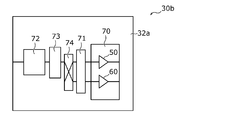
- FIG. 9 is a diagram illustrating the enable control circuit 45 according to the ninth embodiment. More specifically, FIG. 9A is a circuit diagram of the enable control circuit 45. Here, a circuit example of the monolithic semiconductor device 10f in which the enable control circuit 45 is added to the monolithic semiconductor device 10c according to the fourth embodiment is shown. 9 (b) and 9 (c) show the voltage dependence of the enable control terminal 46 in (a) of FIG. That is, FIG. 9B shows the voltage of the enable control terminal 46 (horizontal axis), the voltage of the first bias terminal 15 (vertical axis, alternate long and short dash line), and the gate voltage of the first transistor 12 (vertical axis, solid line). Shows the relationship with. Note that FIG. 9B also shows the first transistor 12 threshold voltage (broken line). FIG. 9C shows the relationship between the voltage of the enable control terminal 46 (horizontal axis) and the drain current of the first transistor 12 (vertical axis).
- an enable control circuit 45 for controlling the active state of the bias voltage applied to the gate of the first transistor 12 is formed on the substrate 11 of the monolithic semiconductor device 10f. Further, the board 11 is provided with an enable control terminal 46 which is an input terminal of the enable control circuit 45 and an enable output terminal 47 which is an output terminal of the enable control circuit 45 and is connected to the first bias terminal 15. There is. A voltage lower than the threshold voltage of the first transistor 12 is applied to the second bias terminal 16.
- the enable control circuit 45 selectively selects a voltage lower than or higher than the threshold voltage of the first transistor 12 according to a change in voltage (High voltage / Low voltage) of 0 V or more applied to the enable control terminal 46. It is a circuit composed of a switch element or the like that outputs from the enable output terminal 47.
- the enable control terminal 46 of the enable control circuit 45 when a high voltage is input to the enable control terminal 46 of the enable control circuit 45, a voltage higher than the threshold voltage of the first transistor 12 is output from the enable output terminal 47, and the voltage is output to the first bias terminal 15. It is applied ((b) in FIG. 9).
- the voltage applied to the first bias terminal 15 is divided by the first resistor 22 and the second resistor 23 of the second bias circuit 20a.
- the first resistor 22 and the second resistor 23 are set so that the voltage dividing voltage is higher than the threshold voltage of the first transistor 12.
- the gate voltage of the first transistor 12 becomes higher than the threshold voltage of the first transistor 12, and the drain current flows on ((c) of FIG. 9).
- the enable control circuit 45 configured in this way can switch the first transistor 12 between the off state and the on state according to the voltage of 0 V or more applied to the enable control terminal 46. .. Therefore, as compared with the case where the power supply voltage is fixedly applied to the first bias terminal 15, the drain current can be easily reduced and the power consumption is reduced when the amplification operation is not performed.
- the enable control circuit 45 is any one of the first to eighth embodiments. It may be added to the semiconductor device.
- the enable control circuit 45 may be formed on a semiconductor substrate or a submount substrate different from the monolithic semiconductor device 10c, and may be connected to the monolithic semiconductor device 10c by wiring, wires, or the like.
- FIG. 10 is a plan layout view of the hybrid semiconductor device 30a according to the tenth embodiment.
- the hybrid semiconductor device 30a includes a submount substrate 32 having a rectangular shape in a plan view, and a monolithic semiconductor device 10f according to the ninth embodiment mounted on the submount substrate 32.
- the submount substrate 32 is a substrate made of resin, ceramic, or the like, and a plurality of substrate terminals 33 are formed on the outer periphery thereof.
- the board terminal 33 includes a high frequency signal input board terminal 33a and an enable control input board terminal 33b.
- the high-frequency signal input board terminal 33a is arranged on the first outer periphery of the four outer periphery of the submount substrate 32, passes through the wiring 34a on the submount substrate 32 and the wire 35a, and is the gate of the monolithic semiconductor device 10f. It is connected to the terminal 13.
- the enable control input board terminal 33b is a board terminal excluding the corner board terminal position on the second outer periphery excluding the outer periphery on which the high frequency signal input board terminal 33a is arranged among the four outer periphery of the submount substrate 32. It is arranged at a position and is connected to the enable control terminal 46 of the monolithic semiconductor device 10f via the wiring 34b on the submount substrate 32 and the wire 35b.
- the circuit can be applied to a semiconductor device having a bias circuit including at least two transistors, and can be mixed from the bias terminal.
- a circuit that suppresses noise and has an effect of reducing RF leakage to a bias circuit will be described.
- FIG. 11 is a circuit diagram of the noise suppression circuit according to the eleventh embodiment.
- a circuit example in which a fifth resistor 26 as a noise suppression circuit is added to the first bias circuit 20 according to the first embodiment is shown.
- the fifth resistor 26 is connected between the bias voltage output node of the first bias circuit 20 (that is, the connection point between the first resistor 22 and the drain terminal of the second transistor 21) and the gate of the first transistor 12. It is a resistance element.
- the noise When noise is superimposed on the second bias terminal 16, the noise is applied to the gate terminal 13 of the first transistor 12 via the capacitance between the gate and drain of the second transistor 21, and is amplified by the first transistor 12. Is output.
- the fifth resistor 26 since the fifth resistor 26 is connected between the bias voltage output node of the first bias circuit 20 and the gate of the first transistor 12, the noise mixed from the second bias terminal 16 is generated. , The fifth resistor 26 attenuates, and as a result, the amount of noise input to the gate terminal 13 of the first transistor 12 is reduced.
- the circuit can be applied to a semiconductor device having a bias circuit including at least two transistors, and noise that can be mixed from the bias terminal. Another circuit that suppresses the above will be described.
- FIG. 12 is a circuit diagram of the noise suppression circuit according to the twelfth embodiment.
- a circuit example in which a sixth resistor 27 as a noise suppression circuit is added to the first bias circuit 20 according to the first embodiment is shown.
- the sixth resistor 27 is a resistance element connected between the second bias terminal 16 that supplies the power supply voltage to the first bias circuit 20 and the gate of the second transistor 21.
- the noise When noise is superimposed on the second bias terminal 16, the noise is applied to the gate terminal 13 of the first transistor 12 via the capacitance between the gate and drain of the second transistor 21, and is amplified by the first transistor 12. Is output.
- the sixth resistor 27 since the sixth resistor 27 is connected between the second bias terminal 16 and the gate of the second transistor 21, the noise mixed from the second bias terminal 16 is the sixth resistor 27. As a result, the amount of noise input to the gate terminal 13 of the first transistor 12 is reduced.
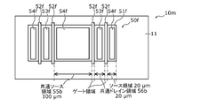
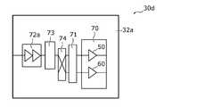
- FIG. 13 is a diagram illustrating 10 g of the monolithic semiconductor device according to the thirteenth embodiment. More specifically, FIG. 13A is a plan layout diagram of the monolithic semiconductor device 10g, and FIG. 13B is a circuit diagram of the monolithic semiconductor device 10g used for the Doherty amplifier.
- the monolithic semiconductor device 10g includes a substrate 11, a HEMT type first transistor 50 formed on the substrate 11 for power amplification, and a HEMT type first transistor 50 formed on the substrate 11 and having a larger conduction current capacity than the first transistor 50. It has a second transistor 60 for power amplification.
- the monolithic semiconductor device 10g is used in a Doherty amplifier circuit in which the first transistor 50 is a carrier amplifier and the second transistor 60 is a peak amplifier.
- the cross-sectional structure of the first transistor 50 and the second transistor 60 is the same as the structure shown in FIG. 1 (b). That is, a first nitride semiconductor layer 102 composed of GaN or the like is formed on the substrate 11, and a band gap is formed on the first nitride semiconductor layer 102 as compared with the first nitride semiconductor layer 102. A second nitride semiconductor layer 103 composed of a large AlGaN or the like is formed, and a drain electrode 110 and a gate electrode 111 separated by an insulating layer 106 composed of SiN or the like are formed on the second nitride semiconductor layer 103.
- the source electrode 112 is formed, and the two-dimensional electron gas layer 107 is formed at the interface between the first nitride semiconductor layer 102 and the second nitride semiconductor layer 103.
- the first transistor 50 and the second transistor 60 are HEMT type transistors formed on the substrate 11 and composed of the first nitride semiconductor layer 102 and the second nitride semiconductor layer 103.
- the first transistor 50 is composed of four parallel-connected unit transistors formed in a continuous first active region 51, and is composed of four gate electrodes 52. It has two drain electrodes 53 and three source electrodes 54.
- the second transistor 60 is composed of six parallel-connected unit transistors formed in a continuous second active region 61, and includes six gate electrodes 62, three drain electrodes 63, and four drain electrodes 63. It has a source electrode 64.
- the gate electrode width per gate electrode of the first transistor 50 is the gate electrode width of the first unit (here, 200 ⁇ m), and the gate electrode width per gate electrode of the second transistor 60 is the second unit gate.
- the electrode width (here, 200 ⁇ m), the number of gate electrodes of the first transistor 50 is the number of first gate electrodes (here, 4), and the number of gate electrodes of the second transistor 60 is the number of second gate electrodes (here, 6).
- the value (1200) obtained by multiplying the second unit gate electrode width and the number of second gate electrodes is larger than the value (800) obtained by multiplying the first unit gate electrode width and the number of first gate electrodes.
- 10 g of the monolithic semiconductor device is configured. With such a configuration, the conduction current capacity of the second transistor 60 becomes larger than the conduction current capacity of the first transistor 50.
- the conduction current capacity of the second transistor 60 which is a peak amplifier
- the conduction current capacity of the first transistor 50 which is a carrier amplifier
- the first transistor 50 (carrier amplifier) operates by being given a higher gate voltage than the second transistor 60 (peak amplifier). Normally, it is necessary to adjust the gate voltage for each of the first transistor 50 (carrier amplifier) and the second transistor 60 (peak amplifier). However, in the present embodiment, since both are configured on the same substrate 11, the threshold voltages of the two are substantially equal, and as shown in FIG. 13B, for example, the level shift circuit 58 By connecting both gate terminals via the above, it is possible to determine the gate voltage of both the first transistor 50 (carrier amplifier) and the second transistor 60 (peak amplifier) with a single gate voltage adjustment. , The number of steps for gate voltage adjustment can be halved.
- FIG. 14 is a diagram illustrating the monolithic semiconductor device 10h according to the thirteenth embodiment. More specifically, FIG. 14A is a plan layout view of the monolithic semiconductor device 10h.
- FIG. 14B shows the ratio (PA size / CA size, horizontal axis) between the size of the peak amplifier (second transistor 60) and the size of the carrier amplifier (first transistor 50) of the monolithic semiconductor device 10h, and the heat. It is a figure which shows the relationship between resistance (solid line, left vertical axis) and efficiency (broken line, right vertical axis).
- FIG. 14C is a diagram showing the relationship between the thermal resistance (horizontal axis) and the efficiency (vertical axis) of the monolithic semiconductor device 10h.
- the sizes of the peak amplifier and the carrier amplifier are values obtained by multiplying the unit gate electrode width and the number of gate electrodes, respectively.
- the monolithic semiconductor device 10h according to the present embodiment is used in a Doherty amplifier circuit in which the first transistor 50a is a carrier amplifier and the second transistor 60a is a peak amplifier, as in the thirteenth embodiment.
- the first transistor 50a is composed of four parallel-connected unit transistors formed in a continuous first active region 51a, and is composed of four gate electrodes 52a. It has two drain electrodes 53a and three source electrodes 54a.
- the second transistor 60a is composed of six parallel-connected unit transistors formed in a continuous second active region 61a, and includes six gate electrodes 62a, three drain electrodes 63a, and four drain electrodes 63a. It has a source electrode 64a.
- the first unit gate electrode width which is the gate electrode width per gate electrode of the first transistor 50a
- the second unit gate which is the gate electrode width per gate electrode of the second transistor 60a.
- the electrode width is 215 ⁇ m. Therefore, in the present embodiment, the value (1290) obtained by multiplying the second unit gate electrode width (215 ⁇ m) and the number of second gate electrodes (6) is the first unit gate electrode width (200 ⁇ m) and the first gate.
- the monolithic semiconductor device 10h is configured so that the value (800) obtained by multiplying the number of electrodes (4) is 1.5 times or more and 1.7 times or less. With such a configuration, the conduction current capacity of the second transistor 60a is 1.5 times or more and 1.7 times or less that of the first transistor 50.
- a high-frequency amplifier circuit obtains high efficiency when it operates at a power close to the saturated power. Therefore, if the size of the carrier amplifier (first transistor 50a) that always operates in the Doherty amplifier circuit is reduced, the carrier amplifier becomes saturated power. It operates at close power and high efficiency can be obtained (broken line in FIG. 14B). However, the thermal resistance deteriorates by reducing the size of the carrier amplifier (solid line in FIG. 14B). In a Dougherty amplifier circuit, as shown in FIG. 14B, efficiency above a certain value and thermal resistance below a certain value are generally required.
- the area of the first active region where the first transistor is formed is the area of the second active region where the second transistor is formed in the plan view of the substrate. A monolithic semiconductor device larger than the area will be described.
- FIG. 15 is a plan layout view of the monolithic semiconductor device 10i according to the fifteenth embodiment.
- the monolithic semiconductor device 10i according to the present embodiment is used in a Doherty amplifier circuit in which the first transistor 50b is a carrier amplifier and the second transistor 60b is a peak amplifier, as in the thirteenth embodiment.
- the first transistor 50b is composed of four parallel connected unit transistors formed in a continuous first active region 51b, and has four gate electrodes 52b and two gate electrodes 52b. It has a drain electrode 53b and three source electrodes 54b.
- the second transistor 60b is composed of six parallel connected unit transistors formed in a continuous second active region 61b, and includes six gate electrodes 62b, three drain electrodes 63b, and four drain electrodes 63b. It has a source electrode 64b.
- the first unit gate electrode width which is the gate electrode width per gate electrode of the first transistor 50b
- the second unit gate which is the gate electrode width per gate electrode of the second transistor 60b.
- the electrode width is 200 ⁇ m.
- the length of the first active region 51b is 600 ⁇ m
- the length of the second active region 61b is 500 ⁇ m. Therefore, in the present embodiment, the area of the first active region 51b (120,000 ⁇ m 2 ) is larger than the area of the second active region 61b (100,000 ⁇ m 2 ) in the plan view of the substrate 11.
- the carrier amplifier (first transistor 50b) that always operates has a larger amount of heat generation than the peak amplifier (second transistor 60b) that operates only at the peak power of the signal.
- the area of the first active region 51b in which the first transistor 50b is formed is larger than the area of the second active region 61b in which the second transistor 60b is formed.
- the heat generation sources of the carrier amplifier (first transistor 50b) that generates a larger amount of heat are dispersedly arranged, and the carrier amplifier (first transistor 50b) can be operated at a lower temperature.
- the value obtained by dividing the area of the first active region by the conduction current capacity of the first transistor in the plan view of the substrate determines the area of the second active region as the second.
- a monolithic semiconductor device larger than the value divided by the conduction current capacity of the transistor will be described.
- FIG. 16 is a plan layout view of the monolithic semiconductor device 10j according to the sixteenth embodiment.
- the monolithic semiconductor device 10j according to the present embodiment is used in a Doherty amplifier circuit in which the first transistor 50c is a carrier amplifier and the second transistor 60c is a peak amplifier, as in the thirteenth embodiment.
- the first transistor 50c is composed of four parallel-connected unit transistors formed in a continuous first active region 51c, and has four gate electrodes 52c and two gate electrodes 52c. It has a drain electrode 53c and three source electrodes 54c.
- the second transistor 60c is composed of six parallel-connected unit transistors formed in a continuous second active region 61c, and includes six gate electrodes 62c, three drain electrodes 63c, and four drain electrodes 63c. It has a source electrode 64c.
- the first unit gate electrode width which is the gate electrode width per gate electrode of the first transistor 50c
- the second unit gate which is the gate electrode width per gate electrode of the second transistor 60c.
- the electrode width is 200 ⁇ m.
- the length of the first active region 51c is 400 ⁇ m
- the length of the second active region 61c is 500 ⁇ m. Therefore, in this embodiment, in a plan view of the substrate 11, the area of the first active region 51c is 80000Myuemu 2, the area of the second active region 61c is 100000 2.
- the conduction current capacity of the transistor is proportional to the value obtained by multiplying the unit gate electrode width and the number of gate electrodes, the ratio of the conduction current capacity of the first transistor 50c to the conduction current capacity of the second transistor 60c. Is 2: 3.
- the value (40,000) obtained by dividing the area (80000 ⁇ m 2 ) of the first active region 51c by the conduction current capacity (2) of the first transistor 50c is the second activity. It is larger than the value (about 33333) obtained by dividing the area of the region 61c (100,000 ⁇ m 2 ) by the conduction current capacity (3) of the second transistor 60c.
- the heat generation sources of the carrier amplifier (first transistor 50c) that generates a larger amount of heat are dispersedly arranged, and the carrier amplifier (first transistor 50c) can be operated at a lower temperature.
- FIG. 17 is a plan layout view of the monolithic semiconductor device 10k according to the seventeenth embodiment. In this figure, only the characteristic planar layout of the first transistor 50d is shown, and the drawing of the second transistor is omitted. More specifically, FIG. 17A shows a planar layout of only the first transistor 50d, and FIG. 17B shows a planar layout of the first transistor 50d including the source wiring.
- the first transistor 50d is composed of four parallel-connected unit transistors formed in a continuous first active region 51d, and is in the first active region 51d.
- Four gate electrodes 52d formed in the gate region, two drain electrodes 53d formed in the drain region in the first active region 51d, and three formed in the source region in the first active region 51d. It has a source electrode 54d of the above.
- the central source electrode 54d is formed in a common source region 55, which is a common source region for two adjacent unit transistors.
- the length of the common source region 55 is 50 ⁇ m.
- the length of the other source region including the source region formed in close contact with the outer periphery of the substrate 11 is 20 ⁇ m.
- the two drain electrodes 53d are formed in a common drain region 56, which is a drain region common to two adjacent unit transistors.
- the length (20 ⁇ m) of the source region formed in close contact with the outer periphery of the substrate 11 in the first direction in which the source region, gate region, and drain region of the plurality of unit transistors constituting the first transistor 50d are lined up is , Shorter than half the length of the common source region 55 (25 ⁇ m).
- the vacant space can be used for heat dissipation, and for example, a bonding pad or the like can be arranged, so that good heat dissipation and chip size can be achieved. It is possible to suppress the increase at the same time.
- the source electrode 54d is connected to the source wiring 54d1 connected to the back surface of the substrate 11 by the via hole 54d2 for grounding.
- the via holes 54d2 are arranged in two rows in order to reduce the source inductance, but since the current in the nearest source region is halved for the via holes at both ends, even if they are in one row. It doesn't matter. With such a layout, it becomes possible to arrange an element such as a bonding pad in the portion directly below the via holes 54d2 in one row at both ends, and high area efficiency is realized.
- FIG. 18 is a plan layout view of the monolithic semiconductor device 10l according to the eighteenth embodiment. In this figure, only the characteristic planar layout of the first transistor 50e is shown, and the drawing of the second transistor is omitted.
- the first transistor 50e is composed of four parallel-connected unit transistors formed in a continuous first active region 51e, and is formed in a gate region in the first active region 51e.
- the central source electrode 54e is formed in a common source region 55a, which is a common source region for two adjacent unit transistors.
- the length of the common source region 55a is 50 ⁇ m.
- the length of the other source region including the source region formed in close contact with the outer periphery of the substrate 11 is 20 ⁇ m.
- the two drain electrodes 53e are formed in a common drain region 56a, which is a drain region common to two adjacent unit transistors.
- the length is 70 ⁇ m, which is longer than half the length of the common source region 55a (25 ⁇ m).
- the vacant space can be used for heat dissipation, and for example, a bonding pad or the like can be arranged, so that a good heat dissipation chip size is increased. Can be suppressed at the same time.
- FIG. 19 is a plan layout view of the monolithic semiconductor device 10 m according to the nineteenth embodiment. In this figure, only the characteristic planar layout of the first transistor 50f is shown, and the drawing of the second transistor is omitted.
- the first transistor 50f is composed of four parallel-connected unit transistors formed in a continuous first active region 51f, and is formed in a gate region in the first active region 51f.
- the central source electrode 54f is formed in a common source region 55b, which is a common source region for two adjacent unit transistors.
- the length of the common source region 55b is 100 ⁇ m.
- the two drain electrodes 53f are formed in a common drain region 56b, which is a drain region common to two adjacent unit transistors.
- the length of the common drain region 56b is 20 ⁇ m.
- the length (100 ⁇ m) of the common source region 55b is the length of the common drain region 56b in the first direction in which the source region, gate region, and drain region of the plurality of unit transistors constituting the first transistor 50f are arranged. Longer than (20 ⁇ m).
- the capacitance formed by the drain region and the back surface of the substrate is equivalent to the capacitance between the drain and source of the transistor, resulting in drain-.
- An increase in capacitance between sources leads to a decrease in the efficiency of the amplifier circuit.
- the heat generation region is widened and the thermal resistance is reduced without increasing the drain-source capacitance. can do.
- FIG. 20 is a plan layout view of the hybrid semiconductor device 30b according to the 20th embodiment.
- the hybrid semiconductor device 30b is a first monolithic semiconductor device 70 and a first monolithic semiconductor which are a submount substrate 32a and a monolithic semiconductor device 10g which constitutes a Doherty amplifier circuit according to the thirteenth embodiment mounted on the submount substrate 32a.
- the output signal from the input matching circuit area 71 for the device 70, the second monolithic semiconductor device 72, the output matching circuit area 73 for the second monolithic semiconductor device 72, and the output matching circuit area 73 is the signal for the first transistor 50. It has a coupler 74 that distributes the signal to the second transistor 60 and outputs the signal to the input matching circuit region 71.
- the second monolithic semiconductor device 72 has an amplifier circuit that amplifies a high frequency signal and outputs it to the first monolithic semiconductor device 70.
- the doherty amplifier circuit and the amplifier circuit in the previous stage thereof are composed of different monolithic semiconductor devices, and therefore, a second monolithic semiconductor device 72 is located between the two.
- the output matching circuit, the coupler 74, and the input matching circuit of the first monolithic semiconductor device 70 can be arranged, and a multi-stage doherty amplifier circuit is realized in a small area.
- FIG. 21 is a plan layout view of the hybrid semiconductor device 30c according to the twenty-first embodiment.
- the hybrid semiconductor device 30c includes a configuration in which a third monolithic semiconductor device 75 is added to the hybrid semiconductor device 30b according to the 20th embodiment.
- the third monolithic semiconductor device 75 has a first bias circuit that applies a bias voltage to the gate of the first transistor 50 included in the first monolithic semiconductor device 70 and the gate of the transistor included in the second monolithic semiconductor device 72.
- the first bias circuit is, for example, the bias circuit according to the first embodiment or the fourth embodiment.
- the bias circuit in the hybrid semiconductor device 30c by having the bias circuit in the hybrid semiconductor device 30c, the bias circuit outside the hybrid semiconductor device 30c becomes unnecessary, and the amplifier circuit can be formed in a small area. It will be realized.
- FIG. 22 is a plan layout view of the hybrid semiconductor device 30d according to the 22nd embodiment.
- the hybrid semiconductor device 30d basically has the same configuration as the hybrid semiconductor device 30b according to the twentieth embodiment.
- the second monolithic semiconductor device 72a constituting the hybrid semiconductor device 30d is composed of a multi-stage amplifier in which a plurality of amplifier circuits are connected in cascade.
- the hybrid semiconductor device 30d since the hybrid semiconductor device 30d according to the present embodiment configured in this way has the second monolithic semiconductor device 72a configured by the multi-stage amplifier, it has a high gain and the strength of the input signal of the hybrid semiconductor device 30d. It is possible to lower it, and highly efficient amplification is possible.
- FIG. 23 is a plan layout view of the hybrid semiconductor device 30e according to the 23rd embodiment.
- the hybrid semiconductor device 30e basically has the same configuration as the hybrid semiconductor device 30b according to the twentieth embodiment.
- the second monolithic semiconductor device 72b constituting the hybrid semiconductor device 30e is composed of a one-stage amplifier.
- the hybrid semiconductor device 30e according to the present embodiment configured in this way has the second monolithic semiconductor device 72b configured by the one-stage amplifier, the area of the second monolithic semiconductor device 72b can be reduced. A high gain amplifier circuit is realized in a small area.
- FIG. 24 is a plan layout view of the hybrid semiconductor device 30f according to the twenty-fourth embodiment.
- the hybrid semiconductor device 30f basically has the same configuration as the hybrid semiconductor device 30e according to the 23rd embodiment.
- the first monolithic semiconductor device 70 and the second monolithic semiconductor device 72b constituting the hybrid semiconductor device 30f are arranged so that the transmission directions of the high frequency signals in each of the first monolithic semiconductor device 70 and the second monolithic semiconductor device 72b are not parallel to each other (in the plan view).
- they are arranged on the submount substrate 32a so as to be orthogonal to each other).
- the coupler 74a is configured by a wiring pattern on the submount substrate 32a. That is, the coupler 74a is arranged between the amplifier circuit of the second monolithic semiconductor device 72b and the first transistor 50 and the second transistor 60 of the first monolithic semiconductor device 70 according to the wiring pattern, and is a second monolithic semiconductor device. The high-frequency output signal from the amplifier circuit of 72b is distributed and transmitted to the respective gates of the first transistor 50 and the second transistor 60.
- the first monolithic semiconductor device 70 and the second monolithic semiconductor device 72b are not parallel to each other in the transmission directions of high-frequency signals, so that the first monolithic semiconductor device 70 and the second monolithic semiconductor device 72b are not parallel to each other.
- the output matching circuit region 73 for the second monolithic semiconductor device 72b can be removed between the monolithic semiconductor device 70 and the second monolithic semiconductor device 72b without arranging the output matching circuit region 73, and the Doherty amplifier circuit is realized in a small area.
- the coupler 74a is composed of the wiring pattern on the submount substrate 32a, a special component for the coupler 74a becomes unnecessary, and a Dougherty amplifier circuit can be realized at low cost.
- FIG. 25 is a plan layout view of the hybrid semiconductor device 30 g according to the 25th embodiment.
- the hybrid semiconductor device 30g basically has the same configuration as the hybrid semiconductor device 30e according to the 23rd embodiment.
- the first preamplifier 150 which is a preamplifier of the first transistor 50
- the second preamplifier 160 which is a preamplifier for the second transistor 60.
- the first monolithic semiconductor device 70a functions as a Doherty amplifier circuit as in the 23rd embodiment.
- the multi-stage amplifier that combines the first front stage amplifier 150 and the first transistor 50 functions as the carrier amplifier of the Doherty amplifier circuit
- the multi-stage amplifier that combines the second front stage amplifier 160 and the second transistor 60 is the Doherty amplifier circuit. Functions as a carrier amplifier.
- the hybrid semiconductor device 30g configured in this way, since the first monolithic semiconductor device 70a is composed of a multi-stage amplifier, the output power of the second monolithic semiconductor device 72b is reduced and the operating current is reduced. It is possible to realize a highly efficient amplifier circuit.
- FIG. 26 is a plan layout view of the hybrid semiconductor device 30h according to the twenty-sixth embodiment.
- the hybrid semiconductor device 30h basically has the same circuit configuration as the hybrid semiconductor device 30g according to the 25th embodiment.
- the first transistor 50 and the second transistor 60 in the 25th embodiment are arranged in the first monolithic semiconductor device 70
- the first pre-stage amplifier 150 and the second pre-stage amplifier Reference numeral 160 denotes a fourth monolithic semiconductor device 76. That is, the first front stage amplifier 150 and the second front stage amplifier 160 are arranged at positions on the submount substrate 32a except for the first monolithic semiconductor device 70.
- the front-stage amplifier and the rear-stage amplifier are arranged in different monolithic semiconductor devices (fourth monolithic semiconductor device 76 and first monolithic semiconductor device 70, respectively). Therefore, the thermal interference between the fourth monolithic semiconductor device 76 and the first monolithic semiconductor device 70 can be reduced, and a high heat dissipation effect can be realized.
- FIG. 27 is a plan layout view of the hybrid semiconductor device 30i according to the 27th embodiment.
- the hybrid semiconductor device 30i is arranged on the submount board 32b, the carrier amplifier 80 and the peak amplifier 81 which are arranged on the submount board 32b and constitute the Doherty amplifier circuit, and the submount board 32b, and is biased to the carrier amplifier 80. It has a bias circuit 82 that applies a voltage, and a coupler 83 that distributes and transmits the input high-frequency signal to each of the carrier amplifier 80 and the peak amplifier 81.
- the carrier amplifier 80 is, for example, the first transistor 12 in the eighth embodiment.
- the peak amplifier 81 is, for example, the third transistor 40 in the eighth embodiment.
- the bias circuit 82 is, for example, the first bias circuit 20 in the eighth embodiment.
- the coupler 83 is, for example, the coupler 74a in the 24th embodiment.
- the bias circuit 82 is provided in the hybrid semiconductor device 30i, the bias circuit outside the hybrid semiconductor device 30i becomes unnecessary, and the area is small. A Doherty amplifier circuit is realized.
- bias circuit 82 may apply a bias voltage not only to the carrier amplifier 80 but also to both the carrier amplifier 80 and the peak amplifier 81.
- FIG. 28 is a plan layout view of the hybrid semiconductor device 30j according to the 28th embodiment.
- the hybrid semiconductor device 30j basically has the same circuit configuration as the hybrid semiconductor device 30i according to the 27th embodiment.
- the carrier amplifier 80 and the peak amplifier 81 are arranged in the same fifth monolithic semiconductor device 77.
- the carrier amplifier 80 and the peak amplifier 81 are composed of a one-stage amplifier.
- the carrier amplifier 80 and the peak amplifier 81 are arranged on the same monolithic semiconductor device, there is a difference in the characteristics of the transistors constituting the two amplifiers. Can be reduced, and a stable Doherty amplifier circuit is realized.
- the Doherty amplifier circuit is composed of a one-stage amplifier, the area of the fifth monolithic semiconductor device 77 can be reduced, and the Doherty amplifier circuit can be realized in a small area. Will be done.
- FIG. 29 is a plan layout view of the hybrid semiconductor device 30k according to the 29th embodiment.
- the hybrid semiconductor device 30k basically has the same circuit configuration as the hybrid semiconductor device 30i according to the 27th embodiment.
- the carrier amplifier 80a and the peak amplifier 81a are arranged in the same sixth monolithic semiconductor device 78. Further, the carrier amplifier 80a and the peak amplifier 81a are composed of a multi-stage amplifier.
- the sixth monolithic semiconductor device 78 is, for example, the first monolithic semiconductor device 70a according to the 25th embodiment.
- the Doherty amplifier circuit is composed of a multi-stage amplifier, a high-gain Doherty amplifier circuit is realized, and as a result, the input signal of the hybrid semiconductor device 30k is realized.
- the strength of the circuit can be reduced, and efficient amplification is realized.
- FIG. 30 is a plan layout view of the monolithic semiconductor device 10n according to the thirtieth embodiment.
- the monolithic semiconductor device 10n includes a substrate 11 and a HEMT type first transistor 50 g and a second transistor 60 g formed on the substrate 11.
- the monolithic semiconductor device 10n is used in a Doherty amplifier circuit in which 50 g of the first transistor is a carrier amplifier and 60 g of a second transistor is a peak amplifier.
- the first transistor 50g and the second transistor 60g are each composed of a plurality of first unit transistors 50g1 and a plurality of second unit transistors 60g1 formed in a continuous active region 57.
- the plurality of first unit transistors 50g1 and the plurality of second unit transistors 60g1 are arranged so that the first unit transistors and the second unit transistors are arranged alternately.
- the cross-sectional structure of the plurality of first unit transistors 50g1 and the plurality of second unit transistors 60g1 is the same as the structure shown in FIG. 1 (b). That is, a first nitride semiconductor layer 102 composed of GaN or the like is formed on the substrate 11, and a band gap is formed on the first nitride semiconductor layer 102 as compared with the first nitride semiconductor layer 102. A second nitride semiconductor layer 103 composed of a large AlGaN or the like is formed, and a drain electrode 110 and a gate electrode 111 separated by an insulating layer 106 composed of SiN or the like are formed on the second nitride semiconductor layer 103.
- the source electrode 112 is formed, and the two-dimensional electron gas layer 107 is formed at the interface between the first nitride semiconductor layer 102 and the second nitride semiconductor layer 103.
- the plurality of first unit transistors 50g1 and the plurality of second unit transistors 60g1 are HEMT type transistors formed on the substrate 11 and composed of the first nitride semiconductor layer 102 and the second nitride semiconductor layer 103.
- the heat generation region of the first unit transistor 50g1 used for the carrier amplifier having a large heat generation is widened, and heat is generated between the two first unit transistors 50g1.
- the thermal resistance can be reduced without increasing the area of the substrate 11.
- FIG. 31 is a plan layout view of the monolithic semiconductor device 10o according to the thirty-one embodiment.
- the monolithic semiconductor device 10o basically has the same circuit configuration as the monolithic semiconductor device 10n according to the thirtieth embodiment.
- the plurality of first unit transistors 50g1 and the plurality of second unit transistors 60g1 are formed adjacent to each other with their respective source regions as common source regions. Therefore, it is different from the embodiment 30.
- each of the plurality of first unit transistors 50g1 has a first gate region in which the gate electrode 52 is formed, a first drain region in which the drain electrode 53 is formed, and a source electrode 54a in the active region 57. And 54b have a first source region formed.
- each of the plurality of second unit transistors 60g1 has a second gate region in which the gate electrode 62 is formed, a second drain region in which the drain electrode 63 is formed, and source electrodes 64a and 64b, respectively, in the active region 57.
- the heat generation region of the first unit transistor 50g1 used for the carrier amplifier having a large heat generation is widened, and heat is generated between the two first unit transistors 50g1.
- the thermal resistance can be reduced without increasing the area of the substrate 11.
- FIG. 32 is a diagram illustrating the monolithic semiconductor device 10p according to the 32nd embodiment. More specifically, FIG. 32 (a) shows a planar layout of the monolithic semiconductor device 10p, and FIG. 32 (b) shows thermal resistance (solid line, left vertical axis) with respect to the length (horizontal axis) of the common source area. And the relationship with the transistor area (solid line, right vertical axis) are shown.
- the monolithic semiconductor device 10p has a substrate 11 and a HEMT type power amplification transistor 90 formed on the substrate 11.
- the transistor 90 is composed of a plurality of unit transistors 90a to 90d formed in a continuous active region 91.
- Each of the plurality of unit transistors 90a to 90d has a source region in which the source electrode 94 is formed, a gate region in which the gate electrode 92 is formed, and a drain region in which the drain electrode 93 is formed in the active region 91.
- Adjacent unit transistors among the plurality of unit transistors 90a to 90d have a common source region 95 having their respective source regions as a common region, or a common drain region 96 having their respective drain regions as a common region.
- the length of the common source region 95 is 200 ⁇ m or more and 340 ⁇ m or less in the direction in which the source region, gate region, and drain region of the plurality of unit transistors 90a to 90d are arranged.
- the cross-sectional structure of the plurality of unit transistors 90a to 90d is the same as the structure shown in FIG. 1B. That is, a first nitride semiconductor layer 102 composed of GaN or the like is formed on the substrate 11, and a band gap is formed on the first nitride semiconductor layer 102 as compared with the first nitride semiconductor layer 102. A second nitride semiconductor layer 103 composed of a large AlGaN or the like is formed, and a drain electrode 110 and a gate electrode 111 separated by an insulating layer 106 composed of SiN or the like are formed on the second nitride semiconductor layer 103.
- the source electrode 112 is formed, and the two-dimensional electron gas layer 107 is formed at the interface between the first nitride semiconductor layer 102 and the second nitride semiconductor layer 103.
- the plurality of unit transistors 90a to 90d are HEMT type transistors formed on the substrate 11 and composed of the first nitride semiconductor layer 102 and the second nitride semiconductor layer 103.
- the thermal resistance As shown in the "transistor area” of FIG. 32 (b), as the length of the common source region increases, the area of the transistor increases almost linearly. Further, as shown in the “thermal resistance” of FIG. 32 (b), as the length of the common source region increases, the distance between the gate regions, which are the main heat generating sources in the amplifier, increases, so that the thermal resistance increases. It will be reduced, but the degree of reduction will be reduced when it exceeds 200 ⁇ m.
- the length of the common source region 95 is 200 ⁇ m or more and 340 ⁇ m or less, low thermal resistance is ensured without unnecessarily increasing the transistor area.
- FIG. 33 is a diagram illustrating the monolithic semiconductor device 10q according to the 33rd embodiment. More specifically, FIG. 33 (a) shows the planar layout of the monolithic semiconductor device 10q, and FIG. 33 (b) shows the phase difference of the signals at both ends of the gate region with respect to the width (horizontal axis) of the gate region. The solid line) and the signal phase difference (broken line) at both ends of the drain region are shown, and FIG. 33 (c) shows the relationship between the signal phase difference at both ends of the drain region and the gain of the transistor.
- the monolithic semiconductor device 10q basically has the same configuration as that of the 32nd embodiment. However, the length of the gate region in the direction orthogonal to the direction in which the source region, gate region and drain region of the plurality of unit transistors 90a to 90d are arranged, that is, the width of the gate region (between (A) and (B) in the figure). Length) is 260 ⁇ m or less.
- the signal In a high frequency amplification transistor, the signal is generally input to one end of the gate, and the output is output from the opposite end of the drain.
- the phase of the signal rotates in the gate region and the drain region, but the phase rotation amount in the gate region is larger than the phase rotation amount in the drain region, so the signal amplified at the input end of the transistor and amplified at the output end of the transistor.
- the phase of the signal is shifted and the width of the gate region and the drain region in the direction orthogonal to the direction in which the source region, the gate region and the drain region are lined up increases, the phase shift increases ((b) in FIG. 33) and the gain increases. It decreases ((c) in FIG. 33).
- the width of the gate region is 260 ⁇ m or less
- the phase difference of the output is suppressed to 15 degrees or less in a signal having a frequency of 3 GHz or more ((b) in FIG. 33)
- the gain is suppressed ((c) in FIG. 33).
- the monolithic semiconductor device and the hybrid semiconductor device of the present disclosure have been described above based on the first to 33rd embodiments, but the present disclosure is not limited to the first to 33rd embodiments. As long as the gist of the present disclosure is not deviated, various modifications that can be conceived by those skilled in the art are applied to the first to 33rd embodiments, and other embodiments constructed by combining some components in the respective embodiments are also available. Included within the scope of this disclosure.
- the monolithic semiconductor device and the hybrid semiconductor device according to the present disclosure can be used as a monolithic semiconductor device and a hybrid semiconductor device including a transistor capable of reducing the number of steps for individually adjusting the gate voltage, for example, as a Doherty amplifier circuit.
Abstract
This monolithic semiconductor device has: a substrate (11); a first nitride semiconductor layer (102) formed on the substrate (11); a second nitride semiconductor layer (103) formed on the first nitride semiconductor layer (102) and having a bandgap larger than that of the first nitride semiconductor layer (102); an HEMT-type first transistor (12) for power amplification which is formed on the substrate (11) and includes the first nitride semiconductor layer (102) and the second nitride semiconductor layer (103); and a first bias circuit (20) which includes an HEMT-type second transistor (21) formed on the substrate (11) and disposed outside a propagation path of a high frequency signal input to the first transistor (12), and which applies a bias voltage to a gate of the first transistor (12).
Description
本開示は、モノリシック半導体装置およびハイブリッド半導体装置に関する。
This disclosure relates to monolithic semiconductor devices and hybrid semiconductor devices.
窒化ガリウム(GaN)等の窒化物半導体を用いた高電子移動度トランジスタ(High Electron Mobility Transistor:HEMT)は、ガリウム砒素系半導体を用いたHEMTに対して10倍以上の電力密度を有する。そのために、窒化物半導体を用いたHEMTをハイパワーデバイスとして用いた増幅回路が提案されている(例えば、特許文献1参照)。
A high electron mobility transistor (HEMT) using a nitride semiconductor such as gallium nitride (GaN) has a power density 10 times or more that of HEMT using a gallium arsenic semiconductor. Therefore, an amplifier circuit using HEMT using a nitride semiconductor as a high power device has been proposed (see, for example, Patent Document 1).
しかしながら、特許文献1の技術では、増幅回路を構成するトランジスタのしきい値電圧についての製造ばらつき(つまり、個体差)が考慮されていないために、製造した増幅回路ごとに、無信号時に出力段のトランジスタを流れるドレイン電流(つまり、アイドル電流)が異なる。アイドル電流により、電力利得、歪、効率等が変化し、それらはトレードオフの関係にある為、所望の性能を得るためにはアイドル電流を一定範囲にする必要がある。増幅回路のアイドル電流は、トランジスタのゲート電圧で調整するが、トランジスタの個体ばらつきのために、一定のゲート電圧でアイドル電流を許容範囲内にすることが困難であり、個々にゲート電圧を調整する必要がある。
However, in the technique of Patent Document 1, since the manufacturing variation (that is, individual difference) about the threshold voltage of the transistors constituting the amplifier circuit is not taken into consideration, the output stage of each manufactured amplifier circuit when there is no signal. The drain current (that is, idle current) flowing through the transistor is different. The idle current changes the power gain, distortion, efficiency, etc., and they are in a trade-off relationship. Therefore, it is necessary to keep the idle current within a certain range in order to obtain the desired performance. The idle current of the amplifier circuit is adjusted by the gate voltage of the transistor, but it is difficult to keep the idle current within the allowable range at a constant gate voltage due to individual variation of the transistor, and the gate voltage is adjusted individually. There is a need.
そこで、本開示は、個々にゲート電圧を調整する工数を削減できるトランジスタを含むモノリシック半導体装置およびハイブリッド半導体装置を提供することを目的とする。
Therefore, an object of the present disclosure is to provide a monolithic semiconductor device and a hybrid semiconductor device including a transistor that can reduce the man-hours for individually adjusting the gate voltage.
上記目的を達成するために、本開示の一形態に係るモノリシック半導体装置は、基板と、前記基板上に形成された第1窒化物半導体層と、前記第1窒化物半導体層の上に形成され、前記第1窒化物半導体層と比べてバンドギャップが大きい第2窒化物半導体層と、前記基板上に形成され、前記第1窒化物半導体層および前記第2窒化物半導体層からなるHEMT型の電力増幅用の第1トランジスタと、前記基板上に形成され、前記第1トランジスタに入力される高周波信号の伝搬経路外に配置されたHEMT型の第2トランジスタを含み、前記第1トランジスタのゲートにバイアス電圧を与える第1バイアス回路とを有する。
In order to achieve the above object, the monolithic semiconductor device according to one embodiment of the present disclosure is formed on a substrate, a first nitride semiconductor layer formed on the substrate, and the first nitride semiconductor layer. , A HEMT type consisting of a second nitride semiconductor layer having a larger band gap than the first nitride semiconductor layer, the first nitride semiconductor layer, and the second nitride semiconductor layer formed on the substrate. A first transistor for power amplification and a HEMT type second transistor formed on the substrate and arranged outside the propagation path of a high-frequency signal input to the first transistor are included in the gate of the first transistor. It has a first bias circuit that gives a bias voltage.
また、上記目的を達成するために、本開示の一形態に係るハイブリッド半導体装置は、上記第1モノリシック半導体装置と、前記第1モノリシック半導体装置とは異なり、抵抗素子を有する第2モノリシック半導体装置とを有し、前記第1バイアス回路の一部として前記抵抗素子が使用されている。
Further, in order to achieve the above object, the hybrid semiconductor device according to one embodiment of the present disclosure includes the first monolithic semiconductor device and the second monolithic semiconductor device having a resistance element, unlike the first monolithic semiconductor device. The resistance element is used as a part of the first bias circuit.
本開示に係るモノリシック半導体装置およびハイブリッド半導体装置により、個々にゲート電圧を調整する工数が削減される。
The monolithic semiconductor device and the hybrid semiconductor device according to the present disclosure reduce the man-hours for individually adjusting the gate voltage.
以下、実施の形態に係る窒化物半導体装置について、図面を参照しながら具体的に説明する。なお、以下で説明する実施の形態は、いずれも本開示の一具体例を示すものである。以下の実施の形態で示される数値、形状、材料、構成要素、構成要素の配置位置および接続形態などは、一例であり、本開示を限定する主旨ではない。また、各図は、必ずしも厳密に図示したものではない。各図において、実質的に同一の構成については同一の符号を付し、重複する説明は省略又は簡略化する場合がある。「基板上」等の「ある物体上」との表現には、その物体に接している場合と、その物体に接していない場合との両方のケースが含まれる。
Hereinafter, the nitride semiconductor device according to the embodiment will be specifically described with reference to the drawings. The embodiments described below are all specific examples of the present disclosure. Numerical values, shapes, materials, components, arrangement positions of components, connection forms, and the like shown in the following embodiments are examples, and are not intended to limit the present disclosure. Moreover, each figure is not necessarily exactly illustrated. In each figure, substantially the same configuration may be designated by the same reference numerals, and duplicate description may be omitted or simplified. The expression "on an object" such as "on a substrate" includes both cases of being in contact with the object and cases of not being in contact with the object.
(実施の形態1)
まず、実施の形態1に係るモノリシック半導体装置について説明する。 (Embodiment 1)
First, the monolithic semiconductor device according to the first embodiment will be described.
まず、実施の形態1に係るモノリシック半導体装置について説明する。 (Embodiment 1)
First, the monolithic semiconductor device according to the first embodiment will be described.
図1は、実施の形態1に係るモノリシック半導体装置10を説明する図である。より詳しくは、図1の(a)は、モノリシック半導体装置10の回路図である。図1の(b)は、図1の(a)における第1トランジスタ12および第2トランジスタ21の断面構造を示す図である。図1の(c)は、第2トランジスタ21のしきい値電圧(つまり、しきい値電圧のばらつき)を横軸とし、無信号時の第2トランジスタ21のドレイン電流(破線)(つまり、アイドル電流)を左縦軸とし、第2トランジスタ21のドレイン電圧(実線)を右縦軸とする、第2トランジスタ21のしきい値電圧依存性を示す特性図である。図1の(d)は、第1トランジスタ12のしきい値電圧(つまり、しきい値電圧のばらつき)を横軸とし、無信号時の第1トランジスタ12のドレイン電流(実線)(つまり、アイドル電流)を縦軸とする、第1トランジスタ12のしきい値電圧依存性を示す特性図である。なお、図1の(d)には、参考として、第1バイアス回路20を接続せずに第1トランジスタ12のゲートバイアスを固定した場合に得られるしきい値電圧依存性(破線)も合わせて図示されている。
FIG. 1 is a diagram illustrating a monolithic semiconductor device 10 according to the first embodiment. More specifically, FIG. 1A is a circuit diagram of the monolithic semiconductor device 10. FIG. 1B is a diagram showing a cross-sectional structure of the first transistor 12 and the second transistor 21 in FIG. 1A. In FIG. 1C, the threshold voltage of the second transistor 21 (that is, the variation of the threshold voltage) is taken as the horizontal axis, and the drain current (broken line) of the second transistor 21 when there is no signal (that is, idle). It is a characteristic diagram which shows the threshold voltage dependence of the 2nd transistor 21 with the left vertical axis | current) and the drain voltage (solid line) of the 2nd transistor 21 as the right vertical axis. In FIG. 1D, the threshold voltage of the first transistor 12 (that is, the variation of the threshold voltage) is taken as the horizontal axis, and the drain current (solid line) of the first transistor 12 when there is no signal (that is, idle). It is a characteristic figure which shows the threshold voltage dependence of the 1st transistor 12 with the current) as a vertical axis. As a reference, FIG. 1D also includes the threshold voltage dependence (broken line) obtained when the gate bias of the first transistor 12 is fixed without connecting the first bias circuit 20. It is illustrated.
モノリシック半導体装置10は、1チップの半導体装置であり、半導体の基板11と、基板11上に形成されたHEMT型の電力増幅用の第1トランジスタ12と、基板11上に形成されたHEMT型の第2トランジスタ21を含み、第1トランジスタ12のゲートにバイアス電圧を与える第1バイアス回路20とを有する。
The monolithic semiconductor device 10 is a one-chip semiconductor device, which is a semiconductor substrate 11, a HEMT type first transistor 12 formed on the substrate 11 for power amplification, and a HEMT type formed on the substrate 11. It includes a second transistor 21, and has a first bias circuit 20 that applies a bias voltage to the gate of the first transistor 12.
第1バイアス回路20は、直列に接続された第1抵抗22、第2トランジスタ21および第2抵抗23で構成される。第1抵抗22と第2トランジスタ21のドレインとの接続点は、第1バイアス回路20のバイアス電圧出力ノードに相当し、第1トランジスタ12のゲートに接続されている。第2トランジスタ21は、第1トランジスタ12に入力される高周波信号の伝搬経路外に配置されている。第2抵抗23は、一端が第2トランジスタ21のソースに接続され、他端が第2トランジスタ21のゲートに接続されている。なお、高周波信号の伝搬経路とは、ゲート端子13に入力された高周波信号の大部分が伝搬されていく経路である。
The first bias circuit 20 is composed of a first resistor 22, a second transistor 21, and a second resistor 23 connected in series. The connection point between the first resistor 22 and the drain of the second transistor 21 corresponds to the bias voltage output node of the first bias circuit 20, and is connected to the gate of the first transistor 12. The second transistor 21 is arranged outside the propagation path of the high frequency signal input to the first transistor 12. One end of the second resistor 23 is connected to the source of the second transistor 21, and the other end is connected to the gate of the second transistor 21. The high-frequency signal propagation path is a path in which most of the high-frequency signal input to the gate terminal 13 is propagated.
さらに、モノリシック半導体装置10には、第1トランジスタ12のゲートに接続されるゲート端子13、第1トランジスタ12のドレインに接続されるドレイン端子14、第1抵抗22の一端に接続される第1バイアス端子15、および、第2抵抗23の一端に接続される第2バイアス端子16が設けられている。なお、第1トランジスタ12のソースは接地されている。また、第1バイアス端子15には、第2バイアス端子16よりも高い電圧が印加される。第1バイアス端子15および第2バイアス端子16の一方は接地されてもよい。
Further, the monolithic semiconductor device 10 has a gate terminal 13 connected to the gate of the first transistor 12, a drain terminal 14 connected to the drain of the first transistor 12, and a first bias connected to one end of the first resistor 22. A terminal 15 and a second bias terminal 16 connected to one end of the second resistor 23 are provided. The source of the first transistor 12 is grounded. Further, a voltage higher than that of the second bias terminal 16 is applied to the first bias terminal 15. One of the first bias terminal 15 and the second bias terminal 16 may be grounded.
図1の(b)に示されるように、Si等で構成される基板11上には、GaN等で構成される第1窒化物半導体層102が形成され、第1窒化物半導体層102の上には、第1窒化物半導体層102と比べてバンドギャップが大きいAlGaN等で構成される第2窒化物半導体層103が形成され、第2窒化物半導体層103の上には、SiN等で構成される絶縁層106で離隔されたドレイン電極110、ゲート電極111およびソース電極112が形成されている。なお、第1窒化物半導体層102と第2窒化物半導体層103との界面には、2次元電子ガス層107が形成されている。また、基板11上には、第1窒化物半導体層102および第2窒化物半導体層103を、他の回路要素から絶縁するための素子分離層104が形成されている。
As shown in FIG. 1B, a first nitride semiconductor layer 102 made of GaN or the like is formed on the substrate 11 made of Si or the like, and is above the first nitride semiconductor layer 102. A second nitride semiconductor layer 103 made of AlGaN or the like having a larger band gap than the first nitride semiconductor layer 102 is formed in the above, and SiN or the like is formed on the second nitride semiconductor layer 103. A drain electrode 110, a gate electrode 111, and a source electrode 112 separated by an insulating layer 106 are formed. A two-dimensional electron gas layer 107 is formed at the interface between the first nitride semiconductor layer 102 and the second nitride semiconductor layer 103. Further, an element separation layer 104 for insulating the first nitride semiconductor layer 102 and the second nitride semiconductor layer 103 from other circuit elements is formed on the substrate 11.
ゲート電極111は、第2窒化物半導体層103とショットキー接合しており、ドレイン電極110およびソース電極112は、熱処理等が施されることで、チャネルとして機能する2次元電子ガス層107とオーミック接続している。このように、第1トランジスタ12および第2トランジスタ21は、基板11上に形成され、第1窒化物半導体層102および第2窒化物半導体層103からなるHEMT型のトランジスタである。
The gate electrode 111 is Schottky-bonded to the second nitride semiconductor layer 103, and the drain electrode 110 and the source electrode 112 are ohmic with the two-dimensional electron gas layer 107 that functions as a channel by being heat-treated or the like. You are connected. As described above, the first transistor 12 and the second transistor 21 are HEMT type transistors formed on the substrate 11 and composed of the first nitride semiconductor layer 102 and the second nitride semiconductor layer 103.
このように構成された本実施の形態に係るモノリシック半導体装置10では、第1バイアス端子15および第2バイアス端子16のそれぞれに適切なバイアス電圧が印可された状態で、ゲート端子13に高周波信号が入力されると、第1トランジスタ12をハイパワーデバイスとする電力増幅が行われ、ドレイン端子14から、電力増幅後の出力信号が出力される。
In the monolithic semiconductor device 10 according to the present embodiment configured in this way, a high-frequency signal is transmitted to the gate terminal 13 in a state where an appropriate bias voltage is applied to each of the first bias terminal 15 and the second bias terminal 16. Upon input, power amplification is performed using the first transistor 12 as a high power device, and the output signal after power amplification is output from the drain terminal 14.
一般的に、トランジスタのドレイン電流は、しきい値電圧とゲートバイアスの差で変化し、ゲートバイアスを固定した場合、製造ばらつきによるしきい値電圧の変化でドレイン電流は大きく変化する、例えば、しきい値電圧が高くなるとドレイン電流は減少する。
Generally, the drain current of a transistor changes due to the difference between the threshold voltage and the gate bias, and when the gate bias is fixed, the drain current changes significantly due to the change in the threshold voltage due to manufacturing variations, for example. The drain current decreases as the threshold voltage increases.
いま、第1トランジスタ12のしきい値電圧が高いほうにばらついたとする。本実施の形態では、同じ基板11上に第1トランジスタ12と同じ構造で形成された第2トランジスタ21もしきい値電圧が高いほうにばらつく。第2トランジスタ21と第2抵抗23とで定電流源回路が構成されるので、第2トランジスタ21のしきい値電圧が高くなると第2トランジスタ21のドレイン電流(つまり、アイドル電流)は減少し(図1の(c))、第2トランジスタ21のドレイン電流と第1抵抗22とで発生する電圧降下量が低下する。その結果、第1トランジスタ12のゲート電圧が上昇するため、第1トランジスタ12のしきい値電圧の上昇と共に第1トランジスタ12のゲートバイアスが上昇する。これにより、ゲートバイアスを固定した場合に比べ、第1トランジスタ12のドレイン電流(つまり、アイドル電流)の低下が抑制される(図1の(d))。よって、本実施の形態により、しきい値電圧のばらつきに応じて第1トランジスタ12のゲート電圧を変化させる第1バイアス回路20により、定電圧源でもアイドル電流を許容範囲内にすることが可能になり、個々にゲート電圧を調整する工数が削減される。
It is assumed that the threshold voltage of the first transistor 12 now varies to the higher side. In the present embodiment, the second transistor 21 formed on the same substrate 11 and having the same structure as the first transistor 12 also varies toward the higher threshold voltage. Since the constant current source circuit is composed of the second transistor 21 and the second resistor 23, the drain current (that is, idle current) of the second transistor 21 decreases as the threshold voltage of the second transistor 21 increases (that is, the idle current). In FIG. 1C), the amount of voltage drop generated by the drain current of the second transistor 21 and the first resistor 22 is reduced. As a result, the gate voltage of the first transistor 12 rises, so that the gate bias of the first transistor 12 rises as the threshold voltage of the first transistor 12 rises. As a result, a decrease in the drain current (that is, idle current) of the first transistor 12 is suppressed as compared with the case where the gate bias is fixed (FIG. 1 (d)). Therefore, according to the present embodiment, the idle current can be kept within the permissible range even with a constant voltage source by the first bias circuit 20 that changes the gate voltage of the first transistor 12 according to the variation of the threshold voltage. Therefore, the number of steps to adjust the gate voltage individually is reduced.
(実施の形態2)
次に、実施の形態2に係るハイブリッド半導体装置について説明する。 (Embodiment 2)
Next, the hybrid semiconductor device according to the second embodiment will be described.
次に、実施の形態2に係るハイブリッド半導体装置について説明する。 (Embodiment 2)
Next, the hybrid semiconductor device according to the second embodiment will be described.
図2は、実施の形態2に係るハイブリッド半導体装置30の回路図である。ハイブリッド半導体装置30は、基本的には、実施の形態1に係るモノリシック半導体装置10と同じ回路構成を備えるが、2つの基板11および11aに分けて形成されている(つまり、2チップの半導体装置で構成される)点で実施の形態1と異なる。
FIG. 2 is a circuit diagram of the hybrid semiconductor device 30 according to the second embodiment. The hybrid semiconductor device 30 basically has the same circuit configuration as the monolithic semiconductor device 10 according to the first embodiment, but is formed separately on two substrates 11 and 11a (that is, a two-chip semiconductor device). It differs from the first embodiment in that (consisting of).
つまり、ハイブリッド半導体装置30は、2つの基板11および11aを備えるとともに、回路要素として、第1トランジスタ12、第2トランジスタ21、第1抵抗22、第2抵抗23、ゲート端子13、ドレイン端子14、第1バイアス端子15、および、第2バイアス端子16を備える。これらの回路要素のうえ、第1トランジスタ12、第2トランジスタ21、ゲート端子13およびドレイン端子14は、基板11上に形成され、第1抵抗22、第2抵抗23、第1バイアス端子15、および、第2バイアス端子16は、基板11a上に形成されている。
That is, the hybrid semiconductor device 30 includes two substrates 11 and 11a, and has the first transistor 12, the second transistor 21, the first resistor 22, the second resistor 23, the gate terminal 13, and the drain terminal 14 as circuit elements. It includes a first bias terminal 15 and a second bias terminal 16. On top of these circuit elements, the first transistor 12, the second transistor 21, the gate terminal 13 and the drain terminal 14 are formed on the substrate 11, and the first resistor 22, the second resistor 23, the first bias terminal 15, and the first bias terminal 15 are formed. , The second bias terminal 16 is formed on the substrate 11a.
基板11を用いて形成されたモノリシック半導体装置を第1モノリシック半導体装置10aと呼び、基板11aを用いて形成されたモノリシック半導体装置を第2モノリシック半導体装置10bと呼ぶことができる。ハイブリッド半導体装置30は、第1モノリシック半導体装置10aおよび第2モノリシック半導体装置10bで構成される。なお、第1モノリシック半導体装置10aと第2モノリシック半導体装置10bとは、ワイヤー、または、図示されないサブマウント基板上に形成された配線パターンを介して接続される。
The monolithic semiconductor device formed by using the substrate 11 can be called the first monolithic semiconductor device 10a, and the monolithic semiconductor device formed by using the substrate 11a can be called the second monolithic semiconductor device 10b. The hybrid semiconductor device 30 is composed of a first monolithic semiconductor device 10a and a second monolithic semiconductor device 10b. The first monolithic semiconductor device 10a and the second monolithic semiconductor device 10b are connected via a wire or a wiring pattern formed on a submount substrate (not shown).
このように構成された本実施の形態に係るハイブリッド半導体装置30によれば、実施の形態1の効果に加えて、2つの基板11および11aに分散されて回路が形成されることによる次の効果が奏される。つまり、第1トランジスタ12のような信号増幅用トランジスタは、動作電流により発熱し、他の回路素子を加熱する場合がある。本実施の形態に係るハイブリッド半導体装置30では、第1抵抗22および第2抵抗23は、第1トランジスタ12とは異なる基板11a上に形成されるので、第1トランジスタ12の発熱による影響を受ける程度が低減され、ハイブリッド半導体装置30の安定した動作が確保される。
According to the hybrid semiconductor device 30 according to the present embodiment configured in this way, in addition to the effect of the first embodiment, the following effect due to the circuit being dispersed on the two substrates 11 and 11a is formed. Is played. That is, the signal amplification transistor such as the first transistor 12 may generate heat due to the operating current and heat other circuit elements. In the hybrid semiconductor device 30 according to the present embodiment, since the first resistor 22 and the second resistor 23 are formed on the substrate 11a different from the first transistor 12, they are affected by the heat generated by the first transistor 12. Is reduced, and stable operation of the hybrid semiconductor device 30 is ensured.
(実施の形態3)
次に、実施の形態3として、実施の形態2における第2モノリシック半導体装置10bの第1抵抗22および第2抵抗23の具体的な構造を説明する。 (Embodiment 3)
Next, as the third embodiment, the specific structures of thefirst resistor 22 and the second resistor 23 of the second monolithic semiconductor device 10b according to the second embodiment will be described.
次に、実施の形態3として、実施の形態2における第2モノリシック半導体装置10bの第1抵抗22および第2抵抗23の具体的な構造を説明する。 (Embodiment 3)
Next, as the third embodiment, the specific structures of the
図3は、実施の形態3に係る第1抵抗22および第2抵抗23を説明する図である。より詳しくは、図3の(a)は、第1抵抗22および第2抵抗23の平面レイアウトを示す。図3の(b)は、このような第1抵抗22および第2抵抗23を備える実施の形態2に係る第1トランジスタ12のドレイン電流を示す。図3の(b)において、横軸は、第1抵抗22の抵抗値を第2抵抗23の抵抗値で除した値(抵抗比)を示し、縦軸は、第1トランジスタ12のドレイン電流を示す。なお、図3の(b)では、本実施の形態における値の範囲に加えて、参考としての通常の場合(本実施の形態における平面レイアウトの特徴を有しない場合)における値の範囲も図示されている。
FIG. 3 is a diagram for explaining the first resistor 22 and the second resistor 23 according to the third embodiment. More specifically, FIG. 3A shows a planar layout of the first resistor 22 and the second resistor 23. FIG. 3B shows the drain current of the first transistor 12 according to the second embodiment including the first resistor 22 and the second resistor 23. In FIG. 3B, the horizontal axis represents the value (resistance ratio) obtained by dividing the resistance value of the first resistor 22 by the resistance value of the second resistor 23, and the vertical axis represents the drain current of the first transistor 12. Shown. In addition, in FIG. 3B, in addition to the range of values in the present embodiment, the range of values in the normal case as a reference (when the feature of the plane layout in the present embodiment is not provided) is also shown. ing.
図3の(a)に示されるように、第1抵抗22および第2抵抗23は、第2モノリシック半導体装置10bの平面視において、これら2つの第1抵抗22および第2抵抗23の間に他の素子を挟まず隣接し、それぞれの抵抗素子を流れる電流の方向が同一となるように配置されている。
As shown in FIG. 3A, the first resistor 22 and the second resistor 23 are placed between the two first resistor 22 and the second resistor 23 in the plan view of the second monolithic semiconductor device 10b. The elements are adjacent to each other without sandwiching them, and are arranged so that the directions of the currents flowing through the respective resistance elements are the same.
第1抵抗22および第2抵抗23の抵抗値の比が変化すると第1トランジスタ12のゲート電圧が変化し、第1トランジスタ12のドレイン電流が変化するが、本実施の形態では、図3の(a)に示されるように、第1抵抗22および第2抵抗23は、同一構造、同一幅(電流が流れる方向に直交する方向の長さが同一)、同一電流方向となるように形成されているので、第1抵抗22および第2抵抗23の抵抗比に対する製造ばらつきの影響が低減される。その結果、図3の(b)に示されるように、このような同一性を有する第1抵抗22および第2抵抗23を備える実施の形態2に係る第1トランジスタ12のドレイン電流のばらつきは、このような同一性を有しない第1抵抗および第2抵抗で構成されるケース(通常のケース)に比べ、低減される。
When the ratio of the resistance values of the first resistor 22 and the second resistor 23 changes, the gate voltage of the first transistor 12 changes and the drain current of the first transistor 12 changes. In this embodiment, (1) in FIG. As shown in a), the first resistor 22 and the second resistor 23 are formed so as to have the same structure, the same width (the same length in the direction orthogonal to the current flow direction), and the same current direction. Therefore, the influence of manufacturing variation on the resistance ratios of the first resistor 22 and the second resistor 23 is reduced. As a result, as shown in FIG. 3B, the variation in the drain current of the first transistor 12 according to the second embodiment including the first resistor 22 and the second resistor 23 having such an identity is This is reduced as compared with the case (normal case) composed of the first resistor and the second resistor having no such identity.
(実施の形態4)
次に、実施の形態4に係るモノリシック半導体装置について説明する。 (Embodiment 4)
Next, the monolithic semiconductor device according to the fourth embodiment will be described.
次に、実施の形態4に係るモノリシック半導体装置について説明する。 (Embodiment 4)
Next, the monolithic semiconductor device according to the fourth embodiment will be described.
図4は、実施の形態4に係るモノリシック半導体装置10cを説明する図である。より詳しくは、図4の(a)は、モノリシック半導体装置10cの回路図を示す。図4の(b)は、第2バイアス端子16にノイズが印加された場合の第1トランジスタ12のゲート端子おけるノイズ電力(縦軸)についての、第2抵抗23の抵抗値(横軸)による依存性を示す。なお、図4の(b)には、参考として、第2抵抗23が存在しない(短絡されている)通常の場合のノイズ電力(破線)も合わせて図示されている。
FIG. 4 is a diagram illustrating the monolithic semiconductor device 10c according to the fourth embodiment. More specifically, FIG. 4A shows a circuit diagram of the monolithic semiconductor device 10c. FIG. 4B shows the resistance value (horizontal axis) of the second resistor 23 with respect to the noise power (vertical axis) at the gate terminal of the first transistor 12 when noise is applied to the second bias terminal 16. Shows dependencies. In addition, in FIG. 4B, for reference, the noise power (broken line) in the normal case where the second resistor 23 does not exist (short-circuited) is also shown.
図4の(a)に示されるように、モノリシック半導体装置10cは、基板11と、基板11上に形成されたHEMT型の電力増幅用の第1トランジスタ12と、第1トランジスタ12のゲートにバイアス電圧を与える第2バイアス回路20aとを有する。第2バイアス回路20aは、少なくとも2つの抵抗素子として、直列に接続された第1抵抗22および第2抵抗23を含む。バイアス電圧は、第1抵抗22および第2抵抗23によって生成される分圧電圧である。なお、第1トランジスタ12が第1窒化物半導体層102および第2窒化物半導体層103からなるトランジスタであることは、実施の形態1と同様である。
As shown in FIG. 4A, the monolithic semiconductor device 10c biases the substrate 11, the HEMT type first transistor 12 for power amplification formed on the substrate 11, and the gate of the first transistor 12. It has a second bias circuit 20a that applies a voltage. The second bias circuit 20a includes a first resistor 22 and a second resistor 23 connected in series as at least two resistance elements. The bias voltage is a voltage divider voltage generated by the first resistor 22 and the second resistor 23. It should be noted that the first transistor 12 is a transistor composed of the first nitride semiconductor layer 102 and the second nitride semiconductor layer 103, as in the first embodiment.
信号増幅用トランジスタである第1トランジスタ12のゲートバイアスは外部より印加されるため、ノイズが重畳される場合があるが、本実施の形態では、第1トランジスタ12のゲート端子は第2抵抗23を介して基板11外に接続されるため、外来からのノイズは第2抵抗23によって減衰して第1トランジスタ12のゲート端子に入力される。その結果、図4の(b)に示されるように、第2抵抗23が存在しない(短絡されている)場合に比べ、外来からのノイズによる影響が低減される。
Since the gate bias of the first transistor 12, which is a signal amplification transistor, is applied from the outside, noise may be superimposed. However, in the present embodiment, the gate terminal of the first transistor 12 has a second resistor 23. Since it is connected to the outside of the substrate 11 via the substrate 11, noise from the outside is attenuated by the second resistor 23 and input to the gate terminal of the first transistor 12. As a result, as shown in FIG. 4B, the influence of noise from the outside is reduced as compared with the case where the second resistor 23 does not exist (short-circuited).
(実施の形態5)
次に、実施の形態5として、実施の形態4に係るモノリシック半導体装置10cの第1抵抗22および第2抵抗23の具体的な構造を説明する。 (Embodiment 5)
Next, as the fifth embodiment, the specific structures of thefirst resistor 22 and the second resistor 23 of the monolithic semiconductor device 10c according to the fourth embodiment will be described.
次に、実施の形態5として、実施の形態4に係るモノリシック半導体装置10cの第1抵抗22および第2抵抗23の具体的な構造を説明する。 (Embodiment 5)
Next, as the fifth embodiment, the specific structures of the
図5は、実施の形態5に係る第1抵抗22および第2抵抗23の構造図である。より詳しくは、図5の(a)は、第1抵抗22および第2抵抗23の平面レイアウトを示し、図5の(b)は、図5の(a)におけるVV線での断面構造を示す。
FIG. 5 is a structural diagram of the first resistor 22 and the second resistor 23 according to the fifth embodiment. More specifically, FIG. 5A shows the planar layout of the first resistor 22 and the second resistor 23, and FIG. 5B shows the cross-sectional structure of FIG. 5A in the VV line. ..
基板11上に、GaN等で構成される第1窒化物半導体層102が形成され、第1窒化物半導体層102の上には、第1窒化物半導体層102と比べてバンドギャップが大きいAlGaN等で構成される第2窒化物半導体層103が形成され、第2窒化物半導体層103の上には、絶縁層106で離隔された第1電極113および第2電極114が形成されている。なお、第1窒化物半導体層102と第2窒化物半導体層103との界面付近には、2次元電子ガス層107が形成されている。また、基板11上には、第1窒化物半導体層102および第2窒化物半導体層103を、他の回路要素から絶縁するための素子分離層104が形成されている。第1電極113および第2電極114は、熱処理等が施されることで、電気抵抗要素として機能する2次元電子ガス層107とオーミック接続しており、電気抵抗要素の両接続端子として構成されている。
A first nitride semiconductor layer 102 composed of GaN or the like is formed on the substrate 11, and AlGaN or the like having a larger band gap than the first nitride semiconductor layer 102 is formed on the first nitride semiconductor layer 102. A second nitride semiconductor layer 103 composed of the above is formed, and a first electrode 113 and a second electrode 114 separated by an insulating layer 106 are formed on the second nitride semiconductor layer 103. A two-dimensional electron gas layer 107 is formed near the interface between the first nitride semiconductor layer 102 and the second nitride semiconductor layer 103. Further, an element separation layer 104 for insulating the first nitride semiconductor layer 102 and the second nitride semiconductor layer 103 from other circuit elements is formed on the substrate 11. The first electrode 113 and the second electrode 114 are ohmic-connected to the two-dimensional electron gas layer 107 that functions as an electric resistance element by being subjected to heat treatment or the like, and are configured as both connection terminals of the electric resistance element. There is.
このように構成された本実施の形態に係る第1抵抗22および第2抵抗23は、2次元電子ガス層が電気抵抗要素として機能するので、高温時に抵抗値が上昇する特性を持つ。よって、本実施の形態に係る第1抵抗22および第2抵抗23を、実施の形態4に係るモノリシック半導体装置10cにおける第2バイアス回路20aの抵抗素子(第1抵抗22および第2抵抗23)として用いることにより、工程を追加することなく、抵抗を集積化する事が可能になり、高温時に第2バイアス回路20aに流れる電流が低減される。
The first resistor 22 and the second resistor 23 according to the present embodiment configured in this way have a characteristic that the resistance value increases at a high temperature because the two-dimensional electron gas layer functions as an electric resistance element. Therefore, the first resistor 22 and the second resistor 23 according to the present embodiment are used as resistance elements (first resistor 22 and second resistor 23) of the second bias circuit 20a in the monolithic semiconductor device 10c according to the fourth embodiment. By using the resistor, it becomes possible to integrate the resistor without adding a step, and the current flowing through the second bias circuit 20a at a high temperature is reduced.
なお、本実施の形態では、2つの第1抵抗22および第2抵抗23がいずれもが2次元電子ガス層を電気抵抗要素とする抵抗素子であったが、いずれか一方だけが2次元電子ガス層を電気抵抗要素とする抵抗素子であり、他の抵抗素子がチップ抵抗等の通常の抵抗素子であってもよい。
In the present embodiment, the two first resistance 22 and the second resistance 23 are both resistance elements having a two-dimensional electron gas layer as an electric resistance element, but only one of them is a two-dimensional electron gas. It is a resistance element having a layer as an electric resistance element, and other resistance elements may be ordinary resistance elements such as chip resistors.
(実施の形態6)
次に、実施の形態6として、実施の形態4におけるモノリシック半導体装置10cの第1抵抗22および第2抵抗23の具体的な構造を説明する。 (Embodiment 6)
Next, as the sixth embodiment, the specific structures of thefirst resistor 22 and the second resistor 23 of the monolithic semiconductor device 10c according to the fourth embodiment will be described.
次に、実施の形態6として、実施の形態4におけるモノリシック半導体装置10cの第1抵抗22および第2抵抗23の具体的な構造を説明する。 (Embodiment 6)
Next, as the sixth embodiment, the specific structures of the
図6は、実施の形態6に係る第1抵抗22および第2抵抗23を説明する図である。より詳しくは、図6の(a)は、第1抵抗22および第2抵抗23の平面レイアウトを示し、図6の(b)は、このような第1抵抗22および第2抵抗23を備える実施の形態4に係る第1トランジスタ12のドレイン電流を示す。図6の(b)において、横軸は、第1抵抗22の抵抗値を第2抵抗23の抵抗値で除した値(抵抗比)を示し、縦軸は、第1トランジスタ12のドレイン電流を示す。なお、図6の(b)では、本実施の形態における値の範囲に加えて、参考としての通常の場合(本実施の形態における平面レイアウトの特徴を有しない場合)における範囲も図示されている。
FIG. 6 is a diagram for explaining the first resistor 22 and the second resistor 23 according to the sixth embodiment. More specifically, FIG. 6 (a) shows a planar layout of the first resistor 22 and the second resistor 23, and FIG. 6 (b) includes such a first resistor 22 and a second resistor 23. The drain current of the first transistor 12 according to the fourth embodiment is shown. In FIG. 6B, the horizontal axis represents the resistance value of the first resistor 22 divided by the resistance value of the second resistor 23 (resistor ratio), and the vertical axis represents the drain current of the first transistor 12. Shown. In addition, in FIG. 6B, in addition to the range of values in the present embodiment, the range in the normal case as a reference (when it does not have the characteristics of the plane layout in the present embodiment) is also shown. ..
図6の(a)に示されるように、第1抵抗22および第2抵抗23は、モノリシック半導体装置10cの平面視において、これら2つの第1抵抗22および第2抵抗23の間に他の素子を挟まず隣接し、それぞれの抵抗素子に流れる電流方向が同一となるように配置されている。
As shown in FIG. 6A, the first resistor 22 and the second resistor 23 are other elements between the two first resistor 22 and the second resistor 23 in the plan view of the monolithic semiconductor device 10c. Are adjacent to each other without sandwiching them, and are arranged so that the current directions flowing through the respective resistance elements are the same.
第1抵抗22および第2抵抗23の抵抗値の比が変化すると第1トランジスタ12のゲート電圧が変化し、第1トランジスタ12のドレイン電流が変化するが、本実施の形態では、図6の(a)に示されるように、第1抵抗22および第2抵抗23は、同一構造、同一幅、同一電流方向となるように形成されているので、第1抵抗22および第2抵抗23の抵抗比に対する製造ばらつきの影響が低減される。その結果、図6の(b)に示されるように、このような同一性を有する第1抵抗22および第2抵抗23を備える実施の形態2に係る第1トランジスタ12のドレイン電流のばらつきは、このような同一性を有しない第1抵抗および第2抵抗で構成されるケース(通常のケース)に比べ、低減される。
When the ratio of the resistance values of the first resistor 22 and the second resistor 23 changes, the gate voltage of the first transistor 12 changes and the drain current of the first transistor 12 changes. In this embodiment, (1) in FIG. As shown in a), since the first resistor 22 and the second resistor 23 are formed so as to have the same structure, the same width, and the same current direction, the resistance ratio of the first resistor 22 and the second resistor 23 The effect of manufacturing variation on is reduced. As a result, as shown in FIG. 6B, the variation in the drain current of the first transistor 12 according to the second embodiment including the first resistor 22 and the second resistor 23 having such an identity is found. This is reduced as compared with the case (normal case) composed of the first resistor and the second resistor having no such identity.
(実施の形態7)
次に、実施の形態7に係るモノリシック半導体装置について説明する。 (Embodiment 7)
Next, the monolithic semiconductor device according to the seventh embodiment will be described.
次に、実施の形態7に係るモノリシック半導体装置について説明する。 (Embodiment 7)
Next, the monolithic semiconductor device according to the seventh embodiment will be described.
図7は、実施の形態7に係るモノリシック半導体装置10dを説明する図である。より詳しくは、図7の(a)は、モノリシック半導体装置10dの回路図である。図7の(b)は、第2トランジスタ21のしきい値電圧(つまり、しきい値電圧のばらつき)を横軸とし、無信号時の第2トランジスタ21のドレイン電流(破線)(つまり、アイドル電流)を左縦軸とし、第2トランジスタ21のドレイン電圧(実線)を右縦軸とする、第2トランジスタ21のしきい値電圧依存性を示す特性図である。図7の(c)は、第1トランジスタ12のしきい値電圧(つまり、しきい値電圧のばらつき)を横軸とし、無信号時の第1トランジスタ12のドレイン電流(実線)(つまり、アイドル電流)を縦軸とする、第1トランジスタ12のしきい値電圧依存性を示す特性図である。
FIG. 7 is a diagram illustrating the monolithic semiconductor device 10d according to the seventh embodiment. More specifically, FIG. 7A is a circuit diagram of the monolithic semiconductor device 10d. In FIG. 7B, the threshold voltage of the second transistor 21 (that is, the variation of the threshold voltage) is taken as the horizontal axis, and the drain current (broken line) of the second transistor 21 when there is no signal (that is, idle). It is a characteristic diagram which shows the threshold voltage dependence of the 2nd transistor 21 with the left vertical axis | current) and the drain voltage (solid line) of the 2nd transistor 21 as the right vertical axis. In FIG. 7C, the threshold voltage of the first transistor 12 (that is, the variation of the threshold voltage) is taken as the horizontal axis, and the drain current (solid line) of the first transistor 12 when there is no signal (that is, idle). It is a characteristic figure which shows the threshold voltage dependence of the 1st transistor 12 with the current) as a vertical axis.
本実施の形態に係るモノリシック半導体装置10dは、基本的には、実施の形態1に係るモノリシック半導体装置10と同じ回路構成を備える。第1バイアス回路20を構成する第1抵抗22および第2抵抗23が、実施の形態5で説明した2次元電子ガス層を電気抵抗要素とする抵抗素子であり、実施の形態6で説明したように、同一構造、同一幅、同一電流方向となるように形成されている点で、そのような抵抗素子に限定されない実施の形態1と異なる。
The monolithic semiconductor device 10d according to the present embodiment basically has the same circuit configuration as the monolithic semiconductor device 10 according to the first embodiment. The first resistor 22 and the second resistor 23 constituting the first bias circuit 20 are resistance elements having the two-dimensional electron gas layer described in the fifth embodiment as an electric resistance element, and are as described in the sixth embodiment. In addition, it differs from the first embodiment in that it is formed so as to have the same structure, the same width, and the same current direction, and is not limited to such a resistance element.
本実施の形態に係るモノリシック半導体装置10dにおいても、第1トランジスタ12のしきい値電圧が高いほうにばらついた場合に、同じ基板11上に第1トランジスタ12と同じ構造で形成された第2トランジスタ21のしきい値電圧も高いほうにばらつく。第2トランジスタ21と第2抵抗23とで定電流源回路が構成されるので、実施の形態1と同様に、第2トランジスタ21のしきい値電圧が高くなると第2トランジスタ21のドレイン電流は減少し(図7の(b))、第2トランジスタ21のドレイン電流と第1抵抗22とで発生する電圧降下量が低下する。その結果、第1トランジスタ12のゲート電圧が上昇するため、第1トランジスタ12のしきい値電圧の上昇と共に第1トランジスタ12のゲートバイアスが上昇する。これにより、ゲートバイアスを固定した場合に比べ、第1トランジスタ12のドレイン電流(つまり、アイドル電流)の低下が抑制される(図7の(c))。よって、本実施の形態により、しきい値電圧のばらつきに応じて第1トランジスタ12のゲート電圧を変化させる第1バイアス回路20により、定電圧源でもアイドル電流を許容範囲内にすることが可能になり、個々にゲート電圧を調整する工数が削減される。
Also in the monolithic semiconductor device 10d according to the present embodiment, when the threshold voltage of the first transistor 12 varies to the higher side, the second transistor formed on the same substrate 11 with the same structure as the first transistor 12. The threshold voltage of 21 also varies to the higher side. Since the constant current source circuit is composed of the second transistor 21 and the second resistor 23, the drain current of the second transistor 21 decreases as the threshold voltage of the second transistor 21 increases, as in the first embodiment. ((B) in FIG. 7), the amount of voltage drop generated by the drain current of the second transistor 21 and the first resistor 22 is reduced. As a result, the gate voltage of the first transistor 12 rises, so that the gate bias of the first transistor 12 rises as the threshold voltage of the first transistor 12 rises. As a result, a decrease in the drain current (that is, idle current) of the first transistor 12 is suppressed as compared with the case where the gate bias is fixed (FIG. 7 (c)). Therefore, according to the present embodiment, the idle current can be kept within the permissible range even with a constant voltage source by the first bias circuit 20 that changes the gate voltage of the first transistor 12 according to the variation of the threshold voltage. Therefore, the number of steps to adjust the gate voltage individually is reduced.
また、第1バイアス回路20を構成する第1抵抗22および第2抵抗23は、2次元電子ガス層が電気抵抗要素として機能する抵抗素子であり、高温時に抵抗値が上昇する特性を持つので、高温時に第1バイアス回路20に流れる電流が低減される。
Further, the first resistance 22 and the second resistance 23 constituting the first bias circuit 20 are resistance elements in which the two-dimensional electron gas layer functions as an electric resistance element, and have a characteristic that the resistance value increases at a high temperature. The current flowing through the first bias circuit 20 at high temperatures is reduced.
さらに、第1抵抗22および第2抵抗23は、同一構造、同一電流方向等の同一性を有するので、第1トランジスタ12のドレイン電流のばらつきは、このような同一性を有しないケースに比べ、低減される。
Further, since the first resistor 22 and the second resistor 23 have the same structure, the same current direction, and the like, the variation in the drain current of the first transistor 12 is compared with the case where the first resistor 12 does not have such an identity. It will be reduced.
(実施の形態8)
次に、実施の形態8に係るモノリシック半導体装置について説明する。 (Embodiment 8)
Next, the monolithic semiconductor device according to the eighth embodiment will be described.
次に、実施の形態8に係るモノリシック半導体装置について説明する。 (Embodiment 8)
Next, the monolithic semiconductor device according to the eighth embodiment will be described.
図8は、実施の形態8に係るモノリシック半導体装置10eを説明する図である。より詳しくは、図8の(a)は、モノリシック半導体装置10eの回路図であり、図8の(b)~(d)は、それぞれ、モノリシック半導体装置10eの第1~第3平面レイアウト例を示す。
FIG. 8 is a diagram illustrating the monolithic semiconductor device 10e according to the eighth embodiment. More specifically, FIG. 8A is a circuit diagram of the monolithic semiconductor device 10e, and FIGS. 8B to 8D are examples of layouts of the first to third planes of the monolithic semiconductor device 10e, respectively. Shown.
図8の(a)に示されるように、モノリシック半導体装置10eは、実施の形態1に係るモノリシック半導体装置10の構成に加えて、基板11上に形成された、第1窒化物半導体層102および第2窒化物半導体層103からなるHEMT型の電力増幅用の第3トランジスタ40と、第3トランジスタ40のゲートにバイアス電圧を与える第3バイアス回路20bとを有する。
As shown in FIG. 8A, the monolithic semiconductor device 10e includes the first nitride semiconductor layer 102 and the first nitride semiconductor layer 102 formed on the substrate 11 in addition to the configuration of the monolithic semiconductor device 10 according to the first embodiment. It has a HEMT type third transistor 40 for power amplification composed of a second nitride semiconductor layer 103, and a third bias circuit 20b that applies a bias voltage to the gate of the third transistor 40.
第3バイアス回路20bは、直列に接続された第3抵抗24および第4抵抗25で構成される。第3抵抗24と第4抵抗25との接続点は、第3バイアス回路20bのバイアス電圧出力ノードに相当し、第3トランジスタ40のゲートに接続されている。なお、第3バイアス回路20bは、HEMT型のトランジスタを含まない。
The third bias circuit 20b is composed of a third resistor 24 and a fourth resistor 25 connected in series. The connection point between the third resistor 24 and the fourth resistor 25 corresponds to the bias voltage output node of the third bias circuit 20b, and is connected to the gate of the third transistor 40. The third bias circuit 20b does not include a HEMT type transistor.
また、モノリシック半導体装置10eには、実施の形態1における端子に加えて、第3トランジスタ40のゲートに接続されるゲート端子41、第3トランジスタ40のドレインに接続されるドレイン端子42、第3抵抗24の一端に接続される第3バイアス端子43、および、第4抵抗25の一端に接続される第4バイアス端子44が設けられている。第3バイアス端子43には、第4バイアス端子44よりも高い電圧が印加される。第3バイアス端子43および第4バイアス端子44の一方は接地されてもよい。
Further, in the monolithic semiconductor device 10e, in addition to the terminals in the first embodiment, a gate terminal 41 connected to the gate of the third transistor 40, a drain terminal 42 connected to the drain of the third transistor 40, and a third resistor A third bias terminal 43 connected to one end of the 24 and a fourth bias terminal 44 connected to one end of the fourth resistor 25 are provided. A voltage higher than that of the fourth bias terminal 44 is applied to the third bias terminal 43. One of the third bias terminal 43 and the fourth bias terminal 44 may be grounded.
なお、モノリシック半導体装置10eは、第1トランジスタ12をキャリアアンプ、第3トランジスタ40をピークアンプとしたドハティ増幅回路を構成している。ドハティ増幅回路は、キャリアアンプと呼ばれる常時動作するB級またはAB級アンプ、および、ピークアンプと呼ばれるピーク電力時のみ動作するC級アンプの出力が直接結合された構成を備え、出力レベルが比較的低い領域でも良好な効率を有する高周波アンプである。
The monolithic semiconductor device 10e constitutes a Doherty amplifier circuit in which the first transistor 12 is a carrier amplifier and the third transistor 40 is a peak amplifier. The Doherty amplifier circuit has a configuration in which the outputs of a class B or class AB amplifier called a carrier amplifier that operates at all times and a class C amplifier called a peak amplifier that operates only at peak power are directly coupled, and the output level is relatively high. It is a high frequency amplifier that has good efficiency even in a low region.
図8の(b)に示される第1平面レイアウト例では、第1トランジスタ12(キャリアアンプ)と第3トランジスタ40(ピークアンプ)との間での熱および信号の干渉を避けるため、両者の最も近接するゲートの間隔は、基板11の厚みの2倍以上(例えば、基板11の厚みが100μmの場合、200μm以上)に設定されている。また、第1トランジスタ12(キャリアアンプ)の放熱を考慮し、第1トランジスタ12(キャリアアンプ)のゲートと基板11の端との最短距離は、基板11の厚み以上(例えば、基板11の厚みが100μmの場合、100μm以上)に設定されている。なお、本実施の形態では、第1トランジスタ12(キャリアアンプ)および第3トランジスタ40(ピークアンプ)は、櫛型(つまり、マルチフィンガータイプの)トランジスタである。
In the first plane layout example shown in FIG. 8 (b), in order to avoid heat and signal interference between the first transistor 12 (carrier amplifier) and the third transistor 40 (peak amplifier), both are the most. The distance between the adjacent gates is set to be twice or more the thickness of the substrate 11 (for example, 200 μm or more when the thickness of the substrate 11 is 100 μm). Further, in consideration of heat dissipation of the first transistor 12 (carrier amplifier), the shortest distance between the gate of the first transistor 12 (carrier amplifier) and the end of the substrate 11 is equal to or greater than the thickness of the substrate 11 (for example, the thickness of the substrate 11 is large). In the case of 100 μm, it is set to 100 μm or more). In the present embodiment, the first transistor 12 (carrier amplifier) and the third transistor 40 (peak amplifier) are comb-type (that is, multi-finger type) transistors.
第1トランジスタ12(キャリアアンプ)用の第1バイアス回路20は、平面レイアウトにおいて、第1トランジスタ12(キャリアアンプ)の直下に配置され、第1バイアス回路20を構成する第2トランジスタ21は、第1トランジスタ12(キャリアアンプ)のフィンガーが並ぶ方向において第1トランジスタ12(キャリアアンプ)の中央付近に配置されている。
The first bias circuit 20 for the first transistor 12 (carrier amplifier) is arranged directly below the first transistor 12 (carrier amplifier) in the planar layout, and the second transistor 21 constituting the first bias circuit 20 is the first. It is arranged near the center of the first transistor 12 (carrier amplifier) in the direction in which the fingers of the one transistor 12 (carrier amplifier) are lined up.
このようなレイアウトにより、第1トランジスタ12(キャリアアンプ)と第1バイアス回路20を構成する第2トランジスタ21とを近接配置し、これらのフィンガーが並ぶ方向での位置を同一にすることで、両者の特性差が低減される。
With such a layout, the first transistor 12 (carrier amplifier) and the second transistor 21 constituting the first bias circuit 20 are arranged close to each other, and the positions of these fingers in the line-up direction are the same. Characteristic difference is reduced.
図8の(c)に示される第2平面レイアウト例では、第1トランジスタ12(キャリアアンプ)の放熱を考慮し、第1トランジスタ12(キャリアアンプ)のゲートと基板11の端との最短距離は、基板11の厚み以上(例えば、基板11の厚みが100μmの場合、100μm以上)に設定されている。また、第1トランジスタ12(キャリアアンプ)用の第1バイアス回路20は、第1トランジスタ12(キャリアアンプ)と第3トランジスタ40(ピークアンプ)との間に配置され、かつ、第1バイアス回路20を構成する第2トランジスタ21は、第1トランジスタ12(キャリアアンプ)のフィンガーが並ぶ方向を拡張した範囲に配置されている。
In the second plane layout example shown in FIG. 8C, the shortest distance between the gate of the first transistor 12 (carrier amplifier) and the end of the substrate 11 is set in consideration of heat dissipation of the first transistor 12 (carrier amplifier). , The thickness of the substrate 11 or more (for example, when the thickness of the substrate 11 is 100 μm, 100 μm or more) is set. Further, the first bias circuit 20 for the first transistor 12 (carrier amplifier) is arranged between the first transistor 12 (carrier amplifier) and the third transistor 40 (peak amplifier), and the first bias circuit 20 The second transistor 21 constituting the first transistor 12 (carrier amplifier) is arranged in an extended range in the direction in which the fingers of the first transistor 12 (carrier amplifier) are lined up.
なお、第1トランジスタ12(キャリアアンプ)と第2トランジスタ21とのゲート間隔は、50μm以下に近接していてもよい。また、第3トランジスタ40(ピークアンプ)用のバイアス抵抗(第3抵抗24および第4抵抗25)を第2トランジスタ21と50μm以下で近接して配置してもよい。
The gate distance between the first transistor 12 (carrier amplifier) and the second transistor 21 may be close to 50 μm or less. Further, the bias resistors (third resistor 24 and fourth resistor 25) for the third transistor 40 (peak amplifier) may be arranged close to the second transistor 21 at 50 μm or less.
第1トランジスタ12(キャリアアンプ)と第3トランジスタ40(ピークアンプ)との間のスペースに、2つのバイアス回路(第1バイアス回路20および第3バイアス回路20b)を配置することで、第1トランジスタ12(キャリアアンプ)と第3トランジスタ40(ピークアンプ)とが最も近接するゲートの間隔は、基板11の厚みの2倍以上確保され、第1トランジスタ12(キャリアアンプ)と第3トランジスタ40(ピークアンプ)との間での熱および信号の干渉が抑制される。
By arranging two bias circuits (first bias circuit 20 and third bias circuit 20b) in the space between the first transistor 12 (carrier amplifier) and the third transistor 40 (peak amplifier), the first transistor The distance between the gates where the 12 (carrier amplifier) and the third transistor 40 (peak amplifier) are closest to each other is secured at least twice the thickness of the substrate 11, and the first transistor 12 (carrier amplifier) and the third transistor 40 (peak) are secured. Thermal and signal interference with the amplifier) is suppressed.
このようなレイアウトにより、第1トランジスタ12(キャリアアンプ)と第3トランジスタ40(ピークアンプ)との間のスペースをバイアス回路に使用できるため、高い面積効率が実現される。また、第1トランジスタ12(キャリアアンプ)と第1バイアス回路20を構成する第2トランジスタ21とを近接配置し、フィンガーが並ぶ方向に直交する方向での位置を同一にすることで、両者の特性差が低減される。
With such a layout, the space between the first transistor 12 (carrier amplifier) and the third transistor 40 (peak amplifier) can be used for the bias circuit, so that high area efficiency is realized. Further, by arranging the first transistor 12 (carrier amplifier) and the second transistor 21 constituting the first bias circuit 20 in close proximity to each other and making the positions orthogonal to the direction in which the fingers are lined up, the characteristics of both are the same. The difference is reduced.
図8の(d)に示される第3平面レイアウト例では、第1トランジスタ12(キャリアアンプ)と第3トランジスタ40(ピークアンプ)との間での熱および信号の干渉を抑制するため、両者の最も近接するゲートの間隔は、基板11の厚みの2倍以上(例えば、基板11の厚みが100μmの場合、200μm以上)に設定されている。また、第1トランジスタ12(キャリアアンプ)用の第1バイアス回路20は第1トランジスタ12(キャリアアンプ)と基板11の端との間に配置され、かつ、第1バイアス回路20を構成する第2トランジスタ21は第1トランジスタ12(キャリアアンプ)のフィンガーが並ぶ方向を拡張した範囲に配置されている。
In the third plane layout example shown in FIG. 8D, both are suppressed in order to suppress heat and signal interference between the first transistor 12 (carrier amplifier) and the third transistor 40 (peak amplifier). The distance between the closest gates is set to be twice or more the thickness of the substrate 11 (for example, 200 μm or more when the thickness of the substrate 11 is 100 μm). Further, the first bias circuit 20 for the first transistor 12 (carrier amplifier) is arranged between the first transistor 12 (carrier amplifier) and the end of the substrate 11, and the second bias circuit 20 constitutes the first bias circuit 20. The transistor 21 is arranged in an extended range in the direction in which the fingers of the first transistor 12 (carrier amplifier) are lined up.
なお、第1トランジスタ12(キャリアアンプ)と第2トランジスタ21とのゲート間隔は50μm以下に近接していてもよい。
The gate distance between the first transistor 12 (carrier amplifier) and the second transistor 21 may be close to 50 μm or less.
このようなレイアウトにより、第1トランジスタ12(キャリアアンプ)と基板11の端との間のスペースを第1バイアス回路20に使用できるため、高い面積効率が実現される。また、第1トランジスタ12(キャリアアンプ)と第1バイアス回路20を構成する第2トランジスタ21とを近接配置し、フィンガーが並ぶ方向に直交する方向での位置を同一にすることで、両者の特性差が低減される。
With such a layout, the space between the first transistor 12 (carrier amplifier) and the end of the substrate 11 can be used for the first bias circuit 20, so that high area efficiency is realized. Further, by arranging the first transistor 12 (carrier amplifier) and the second transistor 21 constituting the first bias circuit 20 in close proximity to each other and making the positions orthogonal to the direction in which the fingers are lined up, the characteristics of both are the same. The difference is reduced.
一般的に、ドハティ増幅回路では、常時動作するキャリアアンプに比べ、ピーク電力時のみ動作するピークアンプは、低電力領域ではドレイン電流が流れないようなゲート電圧が印加されるため、キャリアアンプと比較してゲートバイアスのばらつきよる特性変動が少ない。本実施の形態に係るモノリシック半導体装置10eでは、ゲートバイアスの変動による影響が大きいキャリアアンプを構成する第1トランジスタ12用のバイアス回路として、第2トランジスタ21を含む第1バイアス回路20が集積されており、これにより、キャリアアンプのばらつき補償効果とピークアンプのチップサイズ抑制の両方が実現される。
In general, in a Doherty amplifier circuit, a peak amplifier that operates only at peak power is applied with a gate voltage that prevents drain current from flowing in the low power region, compared to a carrier amplifier that operates at all times. Therefore, there is little characteristic variation due to variation in gate bias. In the monolithic semiconductor device 10e according to the present embodiment, the first bias circuit 20 including the second transistor 21 is integrated as the bias circuit for the first transistor 12 constituting the carrier amplifier which is greatly affected by the fluctuation of the gate bias. As a result, both the variation compensation effect of the carrier amplifier and the chip size suppression of the peak amplifier are realized.
なお、第1トランジスタ12と第3トランジスタ40の最も近接するゲートの間隔を基板11の厚みの2倍以上に設定するなど、数値条件の記載は、発明者らの経験によるものであり、これに限定されるものではない。
The description of the numerical conditions, such as setting the distance between the gates closest to the first transistor 12 and the third transistor 40 to be at least twice the thickness of the substrate 11, is based on the experience of the inventors. It is not limited.
(実施の形態9)
次に、実施の形態9として、実施の形態1~8におけるバイアス回路に付加し得るイネーブル制御回路について説明する。 (Embodiment 9)
Next, as the ninth embodiment, the enable control circuit that can be added to the bias circuit in the first to eighth embodiments will be described.
次に、実施の形態9として、実施の形態1~8におけるバイアス回路に付加し得るイネーブル制御回路について説明する。 (Embodiment 9)
Next, as the ninth embodiment, the enable control circuit that can be added to the bias circuit in the first to eighth embodiments will be described.
図9は、実施の形態9に係るイネーブル制御回路45を説明する図である。より詳しくは、図9の(a)は、イネーブル制御回路45の回路図である。ここでは、実施の形態4に係るモノリシック半導体装置10cにイネーブル制御回路45が付加されたモノリシック半導体装置10fの回路例が示されている。図9の(b)および(c)は、図9の(a)におけるイネーブル制御端子46の電圧による依存性を示す。つまり、図9の(b)は、イネーブル制御端子46の電圧(横軸)と、第1バイアス端子15の電圧(縦軸、一点鎖線)および第1トランジスタ12のゲート電圧(縦軸、実線)との関係を示す。なお、図9の(b)には、第1トランジスタ12しきい値電圧(破線)も合わせて図示されている。図9の(c)は、イネーブル制御端子46の電圧(横軸)と、第1トランジスタ12のドレイン電流(縦軸)との関係を示す。
FIG. 9 is a diagram illustrating the enable control circuit 45 according to the ninth embodiment. More specifically, FIG. 9A is a circuit diagram of the enable control circuit 45. Here, a circuit example of the monolithic semiconductor device 10f in which the enable control circuit 45 is added to the monolithic semiconductor device 10c according to the fourth embodiment is shown. 9 (b) and 9 (c) show the voltage dependence of the enable control terminal 46 in (a) of FIG. That is, FIG. 9B shows the voltage of the enable control terminal 46 (horizontal axis), the voltage of the first bias terminal 15 (vertical axis, alternate long and short dash line), and the gate voltage of the first transistor 12 (vertical axis, solid line). Shows the relationship with. Note that FIG. 9B also shows the first transistor 12 threshold voltage (broken line). FIG. 9C shows the relationship between the voltage of the enable control terminal 46 (horizontal axis) and the drain current of the first transistor 12 (vertical axis).
図9の(a)に示されるように、モノリシック半導体装置10fの基板11上に、第1トランジスタ12のゲートに与えるバイアス電圧の活性状態を制御するイネーブル制御回路45が形成されている。また、基板11には、イネーブル制御回路45の入力端子であるイネーブル制御端子46、および、イネーブル制御回路45の出力端子であって第1バイアス端子15と接続されたイネーブル出力端子47が設けられている。なお、第2バイアス端子16には、第1トランジスタ12のしきい値電圧より低い電圧が印加されている。
As shown in FIG. 9A, an enable control circuit 45 for controlling the active state of the bias voltage applied to the gate of the first transistor 12 is formed on the substrate 11 of the monolithic semiconductor device 10f. Further, the board 11 is provided with an enable control terminal 46 which is an input terminal of the enable control circuit 45 and an enable output terminal 47 which is an output terminal of the enable control circuit 45 and is connected to the first bias terminal 15. There is. A voltage lower than the threshold voltage of the first transistor 12 is applied to the second bias terminal 16.
イネーブル制御回路45は、イネーブル制御端子46に印加される0V以上の電圧の変化(High電圧/Low電圧)に応じて、第1トランジスタ12のしきい値電圧より低い電圧と高い電圧とを選択的にイネーブル出力端子47から出力するスイッチ素子等で構成される回路である。
The enable control circuit 45 selectively selects a voltage lower than or higher than the threshold voltage of the first transistor 12 according to a change in voltage (High voltage / Low voltage) of 0 V or more applied to the enable control terminal 46. It is a circuit composed of a switch element or the like that outputs from the enable output terminal 47.
いま、イネーブル制御回路45のイネーブル制御端子46にLow電圧が入力されると、イネーブル出力端子47から第1トランジスタ12のしきい値電圧より低い電圧が出力され、その電圧が第1バイアス端子15に印加される(図9の(b))。その結果、第1トランジスタ12は、ゲート電圧が第1トランジスタ12のしきい値電圧より低くなり、ドレイン電流が流れないoff状態になる(図9の(c))。
Now, when a Low voltage is input to the enable control terminal 46 of the enable control circuit 45, a voltage lower than the threshold voltage of the first transistor 12 is output from the enable output terminal 47, and that voltage is output to the first bias terminal 15. It is applied ((b) in FIG. 9). As a result, the gate voltage of the first transistor 12 becomes lower than the threshold voltage of the first transistor 12, and the drain current does not flow in the off state (FIG. 9 (c)).
一方、イネーブル制御回路45のイネーブル制御端子46にHigh電圧が入力されると、イネーブル出力端子47から第1トランジスタ12のしきい値電圧より高い電圧が出力され、その電圧が第1バイアス端子15に印加される(図9の(b))。第1バイアス端子15に印加された電圧は、第2バイアス回路20aの第1抵抗22および第2抵抗23で分圧される。ここで、第1抵抗22および第2抵抗23は、分圧電圧が第1トランジスタ12のしきい値電圧より高くなるように設定されている。その結果、第1トランジスタ12は、ゲート電圧が第1トランジスタ12のしきい値電圧より高くなり、ドレイン電流が流れるon状態になる(図9の(c))。
On the other hand, when a high voltage is input to the enable control terminal 46 of the enable control circuit 45, a voltage higher than the threshold voltage of the first transistor 12 is output from the enable output terminal 47, and the voltage is output to the first bias terminal 15. It is applied ((b) in FIG. 9). The voltage applied to the first bias terminal 15 is divided by the first resistor 22 and the second resistor 23 of the second bias circuit 20a. Here, the first resistor 22 and the second resistor 23 are set so that the voltage dividing voltage is higher than the threshold voltage of the first transistor 12. As a result, the gate voltage of the first transistor 12 becomes higher than the threshold voltage of the first transistor 12, and the drain current flows on ((c) of FIG. 9).
このように構成された本実施の形態に係るイネーブル制御回路45は、イネーブル制御端子46に印加される0V以上の電圧に応じて、第1トランジスタ12をoff状態とon状態とに切り替えることができる。よって、固定的に第1バイアス端子15に電源電圧を印可する場合に比べ、増幅動作を行わない時、容易にドレイン電流を低減する事が可能になり消費電力が低減される。
The enable control circuit 45 according to the present embodiment configured in this way can switch the first transistor 12 between the off state and the on state according to the voltage of 0 V or more applied to the enable control terminal 46. .. Therefore, as compared with the case where the power supply voltage is fixedly applied to the first bias terminal 15, the drain current can be easily reduced and the power consumption is reduced when the amplification operation is not performed.
なお、本実施の形態では、実施の形態4に係るモノリシック半導体装置10cにイネーブル制御回路45が付加された回路例が説明されたが、イネーブル制御回路45は、実施の形態1~8のいずれの半導体装置に付加されてもよい。
In the present embodiment, a circuit example in which the enable control circuit 45 is added to the monolithic semiconductor device 10c according to the fourth embodiment has been described, but the enable control circuit 45 is any one of the first to eighth embodiments. It may be added to the semiconductor device.
なお、イネーブル制御回路45は、モノリシック半導体装置10cとは別の半導体基板上やサブマウント基板上に形成され、モノリシック半導体装置10cと配線やワイヤーなどで接続されてもよい。
The enable control circuit 45 may be formed on a semiconductor substrate or a submount substrate different from the monolithic semiconductor device 10c, and may be connected to the monolithic semiconductor device 10c by wiring, wires, or the like.
(実施の形態10)
次に、実施の形態10に係るハイブリッド半導体装置について説明する。 (Embodiment 10)
Next, the hybrid semiconductor device according to the tenth embodiment will be described.
次に、実施の形態10に係るハイブリッド半導体装置について説明する。 (Embodiment 10)
Next, the hybrid semiconductor device according to the tenth embodiment will be described.
図10は、実施の形態10に係るハイブリッド半導体装置30aの平面レイアウト図である。ハイブリッド半導体装置30aは、平面視で矩形形状を有するサブマウント基板32と、サブマウント基板32に実装された実施の形態9に係るモノリシック半導体装置10fとを有する。
FIG. 10 is a plan layout view of the hybrid semiconductor device 30a according to the tenth embodiment. The hybrid semiconductor device 30a includes a submount substrate 32 having a rectangular shape in a plan view, and a monolithic semiconductor device 10f according to the ninth embodiment mounted on the submount substrate 32.
サブマウント基板32は、樹脂やセラミック等の基板であり、その外周辺に複数の基板端子33が形成されている。基板端子33には、高周波信号入力基板端子33aと、イネーブル制御入力基板端子33bとが含まれる。高周波信号入力基板端子33aは、サブマウント基板32の4つの外周辺のうちの第1外周辺に配置され、サブマウント基板32上の配線34a、および、ワイヤー35aを経て、モノリシック半導体装置10fのゲート端子13に接続されている。イネーブル制御入力基板端子33bは、サブマウント基板32の4つの外周辺のうち、高周波信号入力基板端子33aが配置された外周辺を除いた第2外周辺の、角部基板端子位置を除く基板端子位置に配置され、サブマウント基板32上の配線34b、および、ワイヤー35bを経て、モノリシック半導体装置10fのイネーブル制御端子46に接続されている。
The submount substrate 32 is a substrate made of resin, ceramic, or the like, and a plurality of substrate terminals 33 are formed on the outer periphery thereof. The board terminal 33 includes a high frequency signal input board terminal 33a and an enable control input board terminal 33b. The high-frequency signal input board terminal 33a is arranged on the first outer periphery of the four outer periphery of the submount substrate 32, passes through the wiring 34a on the submount substrate 32 and the wire 35a, and is the gate of the monolithic semiconductor device 10f. It is connected to the terminal 13. The enable control input board terminal 33b is a board terminal excluding the corner board terminal position on the second outer periphery excluding the outer periphery on which the high frequency signal input board terminal 33a is arranged among the four outer periphery of the submount substrate 32. It is arranged at a position and is connected to the enable control terminal 46 of the monolithic semiconductor device 10f via the wiring 34b on the submount substrate 32 and the wire 35b.
このような本実施の形態に係るハイブリッド半導体装置30aのレイアウトにより、高周波信号入力基板端子33aに入力された信号とイネーブル制御入力基板端子33bに入力された信号との干渉が低減され、高周波信号入力基板端子33aに入力された入力信号がイネーブル制御端子46へ漏れることによる誤動作、または、イネーブル制御端子46に入力された雑音が高周波信号入力基板端子33aへ入力されることによる入力信号の劣化が抑制される。
Due to the layout of the hybrid semiconductor device 30a according to the present embodiment as described above, interference between the signal input to the high frequency signal input board terminal 33a and the signal input to the enable control input board terminal 33b is reduced, and the high frequency signal input is performed. Malfunction due to leakage of the input signal input to the board terminal 33a to the enable control terminal 46, or deterioration of the input signal due to the noise input to the enable control terminal 46 being input to the high frequency signal input board terminal 33a is suppressed. Will be done.
(実施の形態11)
次に、実施の形態11として、上記実施の形態1~10に係る半導体装置のうち、少なくとも2つのトランジスタを含むバイアス回路を有する半導体装置に適用し得る回路であって、バイアス端子から混入し得るノイズを抑制し、バイアス回路へのRF漏れ低減効果を有する回路について説明する。 (Embodiment 11)
Next, as the eleventh embodiment, among the semiconductor devices according to the first to tenth embodiments, the circuit can be applied to a semiconductor device having a bias circuit including at least two transistors, and can be mixed from the bias terminal. A circuit that suppresses noise and has an effect of reducing RF leakage to a bias circuit will be described.
図11は、実施の形態11に係るノイズ抑制回路の回路図である。ここでは、実施の形態1に係る第1バイアス回路20に、ノイズ抑制回路としての第5抵抗26を付加した回路例が示されている。第5抵抗26は、第1バイアス回路20のバイアス電圧出力ノード(つまり、第1抵抗22と第2トランジスタ21のドレイン端子との接続点)と第1トランジスタ12のゲートとの間に接続された抵抗素子である。
FIG. 11 is a circuit diagram of the noise suppression circuit according to the eleventh embodiment. Here, a circuit example in which a fifth resistor 26 as a noise suppression circuit is added to the first bias circuit 20 according to the first embodiment is shown. The fifth resistor 26 is connected between the bias voltage output node of the first bias circuit 20 (that is, the connection point between the first resistor 22 and the drain terminal of the second transistor 21) and the gate of the first transistor 12. It is a resistance element.
第2バイアス端子16にノイズが重畳された場合、そのノイズは、第2トランジスタ21のゲート-ドレイン間の容量を介して第1トランジスタ12のゲート端子13に印加され、第1トランジスタ12によって増幅されて出力される。本実施の形態によれば、第1バイアス回路20のバイアス電圧出力ノードと第1トランジスタ12のゲートとの間に第5抵抗26が接続されているので、第2バイアス端子16から混入したノイズは、第5抵抗26によって減衰され、その結果、第1トランジスタ12のゲート端子13に入力されるノイズ量が低減される。
When noise is superimposed on the second bias terminal 16, the noise is applied to the gate terminal 13 of the first transistor 12 via the capacitance between the gate and drain of the second transistor 21, and is amplified by the first transistor 12. Is output. According to the present embodiment, since the fifth resistor 26 is connected between the bias voltage output node of the first bias circuit 20 and the gate of the first transistor 12, the noise mixed from the second bias terminal 16 is generated. , The fifth resistor 26 attenuates, and as a result, the amount of noise input to the gate terminal 13 of the first transistor 12 is reduced.
(実施の形態12)
次に、実施の形態12として、上記実施の形態1~10係る半導体装置のうち、少なくとも2つのトランジスタを含むバイアス回路を有する半導体装置に適用し得る回路であって、バイアス端子から混入し得るノイズを抑制する別の回路について説明する。 (Embodiment 12)
Next, as the twelfth embodiment, among the semiconductor devices according to the first to tenth embodiments, the circuit can be applied to a semiconductor device having a bias circuit including at least two transistors, and noise that can be mixed from the bias terminal. Another circuit that suppresses the above will be described.
図12は、実施の形態12に係るノイズ抑制回路の回路図である。ここでは、実施の形態1に係る第1バイアス回路20に、ノイズ抑制回路としての第6抵抗27を付加した回路例が示されている。第6抵抗27は、第1バイアス回路20に電源電圧を供給する第2バイアス端子16と第2トランジスタ21のゲートとの間に接続された抵抗素子である。
FIG. 12 is a circuit diagram of the noise suppression circuit according to the twelfth embodiment. Here, a circuit example in which a sixth resistor 27 as a noise suppression circuit is added to the first bias circuit 20 according to the first embodiment is shown. The sixth resistor 27 is a resistance element connected between the second bias terminal 16 that supplies the power supply voltage to the first bias circuit 20 and the gate of the second transistor 21.
第2バイアス端子16にノイズが重畳された場合、そのノイズは、第2トランジスタ21のゲート-ドレイン間の容量を介して第1トランジスタ12のゲート端子13に印加され、第1トランジスタ12によって増幅されて出力される。本実施の形態によれば、第2バイアス端子16と第2トランジスタ21のゲートとの間に第6抵抗27が接続されているので、第2バイアス端子16から混入したノイズは、第6抵抗27によって減衰され、その結果、第1トランジスタ12のゲート端子13に入力されるノイズ量が低減される。
When noise is superimposed on the second bias terminal 16, the noise is applied to the gate terminal 13 of the first transistor 12 via the capacitance between the gate and drain of the second transistor 21, and is amplified by the first transistor 12. Is output. According to the present embodiment, since the sixth resistor 27 is connected between the second bias terminal 16 and the gate of the second transistor 21, the noise mixed from the second bias terminal 16 is the sixth resistor 27. As a result, the amount of noise input to the gate terminal 13 of the first transistor 12 is reduced.
(実施の形態13)
次に、実施の形態13に係るモノリシック半導体装置について説明する。 (Embodiment 13)
Next, the monolithic semiconductor device according to the thirteenth embodiment will be described.
次に、実施の形態13に係るモノリシック半導体装置について説明する。 (Embodiment 13)
Next, the monolithic semiconductor device according to the thirteenth embodiment will be described.
図13は、実施の形態13に係るモノリシック半導体装置10gを説明する図である。より詳しくは、図13の(a)は、モノリシック半導体装置10gの平面レイアウト図であり、図13の(b)は、ドハティ増幅器に用いたモノリシック半導体装置10gの回路図である。モノリシック半導体装置10gは、基板11と、基板11上に形成されたHEMT型の電力増幅用の第1トランジスタ50と、基板11上に形成され、第1トランジスタ50より導通電流能力の大きい、HEMT型の電力増幅用の第2トランジスタ60とを有する。モノリシック半導体装置10gは、第1トランジスタ50をキャリアアンプ、第2トランジスタ60をピークアンプとしたドハティ増幅回路に用いられている。
FIG. 13 is a diagram illustrating 10 g of the monolithic semiconductor device according to the thirteenth embodiment. More specifically, FIG. 13A is a plan layout diagram of the monolithic semiconductor device 10g, and FIG. 13B is a circuit diagram of the monolithic semiconductor device 10g used for the Doherty amplifier. The monolithic semiconductor device 10g includes a substrate 11, a HEMT type first transistor 50 formed on the substrate 11 for power amplification, and a HEMT type first transistor 50 formed on the substrate 11 and having a larger conduction current capacity than the first transistor 50. It has a second transistor 60 for power amplification. The monolithic semiconductor device 10g is used in a Doherty amplifier circuit in which the first transistor 50 is a carrier amplifier and the second transistor 60 is a peak amplifier.
なお、第1トランジスタ50および第2トランジスタ60の断面構造は、図1の(b)に示される構造と同じである。つまり、基板11上には、GaN等で構成される第1窒化物半導体層102が形成され、第1窒化物半導体層102の上には、第1窒化物半導体層102と比べてバンドギャップが大きいAlGaN等で構成される第2窒化物半導体層103が形成され、第2窒化物半導体層103の上には、SiN等で構成される絶縁層106で離隔されたドレイン電極110、ゲート電極111およびソース電極112が形成され、第1窒化物半導体層102と第2窒化物半導体層103との界面には、2次元電子ガス層107が形成されている。第1トランジスタ50および第2トランジスタ60は、基板11上に形成され、第1窒化物半導体層102および第2窒化物半導体層103からなるHEMT型のトランジスタである。
The cross-sectional structure of the first transistor 50 and the second transistor 60 is the same as the structure shown in FIG. 1 (b). That is, a first nitride semiconductor layer 102 composed of GaN or the like is formed on the substrate 11, and a band gap is formed on the first nitride semiconductor layer 102 as compared with the first nitride semiconductor layer 102. A second nitride semiconductor layer 103 composed of a large AlGaN or the like is formed, and a drain electrode 110 and a gate electrode 111 separated by an insulating layer 106 composed of SiN or the like are formed on the second nitride semiconductor layer 103. And the source electrode 112 is formed, and the two-dimensional electron gas layer 107 is formed at the interface between the first nitride semiconductor layer 102 and the second nitride semiconductor layer 103. The first transistor 50 and the second transistor 60 are HEMT type transistors formed on the substrate 11 and composed of the first nitride semiconductor layer 102 and the second nitride semiconductor layer 103.
図13の(a)に示されるように、第1トランジスタ50は、連続した第1活性領域51内に形成された4個の並列接続された単位トランジスタで構成され、4本のゲート電極52と、2本のドレイン電極53と、3本のソース電極54とを有する。第2トランジスタ60は、連続した第2活性領域61内に形成された6個の並列接続された単位トランジスタで構成され、6本のゲート電極62と、3本のドレイン電極63と、4本のソース電極64とを有する。
As shown in FIG. 13A, the first transistor 50 is composed of four parallel-connected unit transistors formed in a continuous first active region 51, and is composed of four gate electrodes 52. It has two drain electrodes 53 and three source electrodes 54. The second transistor 60 is composed of six parallel-connected unit transistors formed in a continuous second active region 61, and includes six gate electrodes 62, three drain electrodes 63, and four drain electrodes 63. It has a source electrode 64.
ここで、第1トランジスタ50のゲート電極1本あたりのゲート電極幅を第1単位ゲート電極幅(ここでは、200μm)、第2トランジスタ60のゲート電極1本あたりのゲート電極幅を第2単位ゲート電極幅(ここでは、200μm)、第1トランジスタ50のゲート電極数を第1ゲート電極数(ここでは、4)、第2トランジスタ60のゲート電極数を第2ゲート電極数(ここでは、6)とし、第2単位ゲート電極幅と第2ゲート電極数とを乗じて得られる値(1200)が第1単位ゲート電極幅と第1ゲート電極数とを乗じて得られる値(800)より大きくなるように、モノリシック半導体装置10gが構成されている。このような構成により、第2トランジスタ60の導通電流能力は、第1トランジスタ50の導通電流能力より大きくなる。
Here, the gate electrode width per gate electrode of the first transistor 50 is the gate electrode width of the first unit (here, 200 μm), and the gate electrode width per gate electrode of the second transistor 60 is the second unit gate. The electrode width (here, 200 μm), the number of gate electrodes of the first transistor 50 is the number of first gate electrodes (here, 4), and the number of gate electrodes of the second transistor 60 is the number of second gate electrodes (here, 6). The value (1200) obtained by multiplying the second unit gate electrode width and the number of second gate electrodes is larger than the value (800) obtained by multiplying the first unit gate electrode width and the number of first gate electrodes. As described above, 10 g of the monolithic semiconductor device is configured. With such a configuration, the conduction current capacity of the second transistor 60 becomes larger than the conduction current capacity of the first transistor 50.
ドハティ増幅回路における変調信号のピーク電力と平均電力との比であるPAPRは、ドハティ増幅回路のキャリアアンプの導通電流能力とピークアンプの導通電流能力とが等しい場合、PAPR=6dBで最も高い効率が得られることが知られている。
PAPR, which is the ratio of the peak power to the average power of the modulated signal in the Doherty amplifier circuit, has the highest efficiency at PAPR = 6 dB when the conduction current capacity of the carrier amplifier of the Doherty amplifier circuit and the conduction current capacity of the peak amplifier are equal. It is known to be obtained.
本実施の形態に係るモノリシック半導体装置10gによれば、ピークアンプである第2トランジスタ60の導通電流能力は、キャリアアンプである第1トランジスタ50の導通電流能力より大きいので、PAPRが6dBより大きな信号増幅で、より高い効率をもつドハティ増幅回路が実現される。
According to the monolithic semiconductor device 10g according to the present embodiment, the conduction current capacity of the second transistor 60, which is a peak amplifier, is larger than the conduction current capacity of the first transistor 50, which is a carrier amplifier, so that the PAPR is larger than 6 dB. Amplification realizes a Doherty amplifier circuit with higher efficiency.
第1トランジスタ50(キャリアアンプ)は、第2トランジスタ60(ピークアンプ)より高いゲート電圧が与えられて動作する。通常、第1トランジスタ50(キャリアアンプ)および第2トランジスタ60(ピークアンプ)それぞれにゲート電圧の調整が必要である。ところが、本実施の形態では、両者を同一の基板11上に構成しているので、両者のしきい値電圧はほぼ等しく、図13の(b)に示されるように、例えば、レベルシフト回路58を介して両者のゲート端子を接続することで、一回のゲート電圧調整で、第1トランジスタ50(キャリアアンプ)および第2トランジスタ60(ピークアンプ)両方のゲート電圧を決定することが可能になり、ゲート電圧調整の工数を半分にすることができる。
The first transistor 50 (carrier amplifier) operates by being given a higher gate voltage than the second transistor 60 (peak amplifier). Normally, it is necessary to adjust the gate voltage for each of the first transistor 50 (carrier amplifier) and the second transistor 60 (peak amplifier). However, in the present embodiment, since both are configured on the same substrate 11, the threshold voltages of the two are substantially equal, and as shown in FIG. 13B, for example, the level shift circuit 58 By connecting both gate terminals via the above, it is possible to determine the gate voltage of both the first transistor 50 (carrier amplifier) and the second transistor 60 (peak amplifier) with a single gate voltage adjustment. , The number of steps for gate voltage adjustment can be halved.
(実施の形態14)
次に、実施の形態14として、実施の形態13において、第2トランジスタの導通電流能力が第1トランジスタの1.5倍以上1.7倍以下であるモノリシック半導体装置を説明する。 (Embodiment 14)
Next, as the 14th embodiment, the monolithic semiconductor device in which the conduction current capacity of the second transistor is 1.5 times or more and 1.7 times or less as that of the first transistor will be described.
図14は、実施の形態14に係るモノリシック半導体装置10hを説明する図である。より詳しくは、図14の(a)は、モノリシック半導体装置10hの平面レイアウト図である。図14の(b)は、モノリシック半導体装置10hのピークアンプ(第2トランジスタ60)のサイズとキャリアアンプ(第1トランジスタ50)のサイズとの比(PAサイズ/CAサイズ、横軸)と、熱抵抗(実線、左縦軸)および効率(破線、右縦軸)との関係を示す図である。図14の(c)は、モノリシック半導体装置10hの熱抵抗(横軸)と効率(縦軸)との関係を示す図である。ここで、ピークアンプおよびキャリアアンプのサイズとは、それぞれ単位ゲート電極幅とゲート電極数とを乗じて得られる値のことである。
FIG. 14 is a diagram illustrating the monolithic semiconductor device 10h according to the thirteenth embodiment. More specifically, FIG. 14A is a plan layout view of the monolithic semiconductor device 10h. FIG. 14B shows the ratio (PA size / CA size, horizontal axis) between the size of the peak amplifier (second transistor 60) and the size of the carrier amplifier (first transistor 50) of the monolithic semiconductor device 10h, and the heat. It is a figure which shows the relationship between resistance (solid line, left vertical axis) and efficiency (broken line, right vertical axis). FIG. 14C is a diagram showing the relationship between the thermal resistance (horizontal axis) and the efficiency (vertical axis) of the monolithic semiconductor device 10h. Here, the sizes of the peak amplifier and the carrier amplifier are values obtained by multiplying the unit gate electrode width and the number of gate electrodes, respectively.
本実施の形態に係るモノリシック半導体装置10hは、実施の形態13と同様に、第1トランジスタ50aをキャリアアンプ、第2トランジスタ60aをピークアンプとしたドハティ増幅回路に用いられている。
The monolithic semiconductor device 10h according to the present embodiment is used in a Doherty amplifier circuit in which the first transistor 50a is a carrier amplifier and the second transistor 60a is a peak amplifier, as in the thirteenth embodiment.
図14の(a)に示されるように、第1トランジスタ50aは、連続した第1活性領域51a内に形成された4個の並列接続された単位トランジスタで構成され、4本のゲート電極52aと、2本のドレイン電極53aと、3本のソース電極54aとを有する。第2トランジスタ60aは、連続した第2活性領域61a内に形成された6個の並列接続された単位トランジスタで構成され、6本のゲート電極62aと、3本のドレイン電極63aと、4本のソース電極64aとを有する。
As shown in FIG. 14A, the first transistor 50a is composed of four parallel-connected unit transistors formed in a continuous first active region 51a, and is composed of four gate electrodes 52a. It has two drain electrodes 53a and three source electrodes 54a. The second transistor 60a is composed of six parallel-connected unit transistors formed in a continuous second active region 61a, and includes six gate electrodes 62a, three drain electrodes 63a, and four drain electrodes 63a. It has a source electrode 64a.
ここで、第1トランジスタ50aのゲート電極1本あたりのゲート電極幅である第1単位ゲート電極幅は200μmであり、第2トランジスタ60aのゲート電極1本あたりのゲート電極幅である第2単位ゲート電極幅は、215μmである。よって、本実施の形態では、第2単位ゲート電極幅(215μm)と第2ゲート電極数(6)とを乗じて得られる値(1290)が第1単位ゲート電極幅(200μm)と第1ゲート電極数(4)とを乗じて得られる値(800)の1.5倍以上1.7倍以下となるように、モノリシック半導体装置10hが構成されている。このような構成により、第2トランジスタ60aの導通電流能力は、第1トランジスタ50の1.5倍以上1.7倍以下となる。
Here, the first unit gate electrode width, which is the gate electrode width per gate electrode of the first transistor 50a, is 200 μm, and the second unit gate, which is the gate electrode width per gate electrode of the second transistor 60a. The electrode width is 215 μm. Therefore, in the present embodiment, the value (1290) obtained by multiplying the second unit gate electrode width (215 μm) and the number of second gate electrodes (6) is the first unit gate electrode width (200 μm) and the first gate. The monolithic semiconductor device 10h is configured so that the value (800) obtained by multiplying the number of electrodes (4) is 1.5 times or more and 1.7 times or less. With such a configuration, the conduction current capacity of the second transistor 60a is 1.5 times or more and 1.7 times or less that of the first transistor 50.
一般的に、高周波増幅回路は飽和電力に近い電力で動作すると高い効率が得られるため、ドハティ増幅回路において常時動作するキャリアアンプ(第1トランジスタ50a)のサイズを小さくすると、キャリアアンプは飽和電力に近い電力で動作し高い効率が得られる(図14の(b)の破線)。しかしながら、キャリアアンプのサイズを小さくすることによって熱抵抗が悪化する(図14の(b)の実線)。ドハティ増幅回路では、一般的に、図14の(b)に示されるように、一定値以上の効率と一定値以下の熱抵抗が求められる。
In general, a high-frequency amplifier circuit obtains high efficiency when it operates at a power close to the saturated power. Therefore, if the size of the carrier amplifier (first transistor 50a) that always operates in the Doherty amplifier circuit is reduced, the carrier amplifier becomes saturated power. It operates at close power and high efficiency can be obtained (broken line in FIG. 14B). However, the thermal resistance deteriorates by reducing the size of the carrier amplifier (solid line in FIG. 14B). In a Dougherty amplifier circuit, as shown in FIG. 14B, efficiency above a certain value and thermal resistance below a certain value are generally required.
本実施の形態では、PAサイズ/CAサイズが1.5以上1.7以下(約1.6)であるので、要求値以上の効率と要求値以下の熱抵抗が実現される(図14の(c))。
In the present embodiment, since the PA size / CA size is 1.5 or more and 1.7 or less (about 1.6), efficiency equal to or higher than the required value and thermal resistance equal to or lower than the required value are realized (FIG. 14). (C)).
(実施の形態15)
次に、実施の形態15として、実施の形態13において、基板の平面視で、第1トランジスタが形成されている第1活性領域の面積が、第2トランジスタが形成されている第2活性領域の面積より大きいモノリシック半導体装置を説明する。 (Embodiment 15)
Next, as the fifteenth embodiment, in the thirteenth embodiment, the area of the first active region where the first transistor is formed is the area of the second active region where the second transistor is formed in the plan view of the substrate. A monolithic semiconductor device larger than the area will be described.
図15は、実施の形態15に係るモノリシック半導体装置10iの平面レイアウト図である。本実施の形態に係るモノリシック半導体装置10iは、実施の形態13と同様に、第1トランジスタ50bをキャリアアンプ、第2トランジスタ60bをピークアンプとしたドハティ増幅回路に用いられている。
FIG. 15 is a plan layout view of the monolithic semiconductor device 10i according to the fifteenth embodiment. The monolithic semiconductor device 10i according to the present embodiment is used in a Doherty amplifier circuit in which the first transistor 50b is a carrier amplifier and the second transistor 60b is a peak amplifier, as in the thirteenth embodiment.
図15に示されるように、第1トランジスタ50bは、連続した第1活性領域51b内に形成された4個の並列接続された単位トランジスタで構成され、4本のゲート電極52bと、2本のドレイン電極53bと、3本のソース電極54bとを有する。第2トランジスタ60bは、連続した第2活性領域61b内に形成された6個の並列接続された単位トランジスタで構成され、6本のゲート電極62bと、3本のドレイン電極63bと、4本のソース電極64bとを有する。
As shown in FIG. 15, the first transistor 50b is composed of four parallel connected unit transistors formed in a continuous first active region 51b, and has four gate electrodes 52b and two gate electrodes 52b. It has a drain electrode 53b and three source electrodes 54b. The second transistor 60b is composed of six parallel connected unit transistors formed in a continuous second active region 61b, and includes six gate electrodes 62b, three drain electrodes 63b, and four drain electrodes 63b. It has a source electrode 64b.
ここで、第1トランジスタ50bのゲート電極1本あたりのゲート電極幅である第1単位ゲート電極幅は200μmであり、第2トランジスタ60bのゲート電極1本あたりのゲート電極幅である第2単位ゲート電極幅は、200μmである。また、第1活性領域51bの長さは、600μmであり、第2活性領域61bの長さは、500μmである。よって、本実施の形態では、基板11の平面視において、第1活性領域51bの面積(120000μm2)は、第2活性領域61bの面積(100000μm2)より大きい。
Here, the first unit gate electrode width, which is the gate electrode width per gate electrode of the first transistor 50b, is 200 μm, and the second unit gate, which is the gate electrode width per gate electrode of the second transistor 60b. The electrode width is 200 μm. The length of the first active region 51b is 600 μm, and the length of the second active region 61b is 500 μm. Therefore, in the present embodiment, the area of the first active region 51b (120,000 μm 2 ) is larger than the area of the second active region 61b (100,000 μm 2 ) in the plan view of the substrate 11.
ドハティ増幅回路において、常時動作するキャリアアンプ(第1トランジスタ50b)は、信号のピーク電力時のみ動作するピークアンプ(第2トランジスタ60b)に比べ、発熱量が大きい。本実施の形態に係るモノリシック半導体装置10iでは、第1トランジスタ50bが形成されている第1活性領域51bの面積が、第2トランジスタ60bが形成されている第2活性領域61bの面積より大きいので、より大きな熱を発生するキャリアアンプ(第1トランジスタ50b)の発熱源が分散配置され、キャリアアンプ(第1トランジスタ50b)をより低温で動作させることが可能になる。
In the Dougherty amplifier circuit, the carrier amplifier (first transistor 50b) that always operates has a larger amount of heat generation than the peak amplifier (second transistor 60b) that operates only at the peak power of the signal. In the monolithic semiconductor device 10i according to the present embodiment, the area of the first active region 51b in which the first transistor 50b is formed is larger than the area of the second active region 61b in which the second transistor 60b is formed. The heat generation sources of the carrier amplifier (first transistor 50b) that generates a larger amount of heat are dispersedly arranged, and the carrier amplifier (first transistor 50b) can be operated at a lower temperature.
(実施の形態16)
次に、実施の形態16として、実施の形態13において、基板の平面視で、第1活性領域の面積を第1トランジスタの導通電流能力で除した値が、第2活性領域の面積を第2トランジスタの導通電流能力で除した値より大きいモノリシック半導体装置を説明する。 (Embodiment 16)
Next, as the 16th embodiment, in the 13th embodiment, the value obtained by dividing the area of the first active region by the conduction current capacity of the first transistor in the plan view of the substrate determines the area of the second active region as the second. A monolithic semiconductor device larger than the value divided by the conduction current capacity of the transistor will be described.
図16は、実施の形態16に係るモノリシック半導体装置10jの平面レイアウト図である。本実施の形態に係るモノリシック半導体装置10jは、実施の形態13と同様に、第1トランジスタ50cをキャリアアンプ、第2トランジスタ60cをピークアンプとしたドハティ増幅回路に用いられている。
FIG. 16 is a plan layout view of the monolithic semiconductor device 10j according to the sixteenth embodiment. The monolithic semiconductor device 10j according to the present embodiment is used in a Doherty amplifier circuit in which the first transistor 50c is a carrier amplifier and the second transistor 60c is a peak amplifier, as in the thirteenth embodiment.
図16に示されるように、第1トランジスタ50cは、連続した第1活性領域51c内に形成された4個の並列接続された単位トランジスタで構成され、4本のゲート電極52cと、2本のドレイン電極53cと、3本のソース電極54cとを有する。第2トランジスタ60cは、連続した第2活性領域61c内に形成された6個の並列接続された単位トランジスタで構成され、6本のゲート電極62cと、3本のドレイン電極63cと、4本のソース電極64cとを有する。
As shown in FIG. 16, the first transistor 50c is composed of four parallel-connected unit transistors formed in a continuous first active region 51c, and has four gate electrodes 52c and two gate electrodes 52c. It has a drain electrode 53c and three source electrodes 54c. The second transistor 60c is composed of six parallel-connected unit transistors formed in a continuous second active region 61c, and includes six gate electrodes 62c, three drain electrodes 63c, and four drain electrodes 63c. It has a source electrode 64c.
ここで、第1トランジスタ50cのゲート電極1本あたりのゲート電極幅である第1単位ゲート電極幅は200μmであり、第2トランジスタ60cのゲート電極1本あたりのゲート電極幅である第2単位ゲート電極幅は、200μmである。また、第1活性領域51cの長さは、400μmであり、第2活性領域61cの長さは、500μmである。よって、本実施の形態では、基板11の平面視において、第1活性領域51cの面積は、80000μm2であり、第2活性領域61cの面積は、100000μm2である。
Here, the first unit gate electrode width, which is the gate electrode width per gate electrode of the first transistor 50c, is 200 μm, and the second unit gate, which is the gate electrode width per gate electrode of the second transistor 60c. The electrode width is 200 μm. The length of the first active region 51c is 400 μm, and the length of the second active region 61c is 500 μm. Therefore, in this embodiment, in a plan view of the substrate 11, the area of the first active region 51c is 80000Myuemu 2, the area of the second active region 61c is 100000 2.
また、トランジスタの導通電流能力は、単位ゲート電極幅とゲート電極数とを乗じて得られる値に比例するので、第1トランジスタ50cの導通電流能力と、第2トランジスタ60cの導通電流能力との比は、2:3となる。
Further, since the conduction current capacity of the transistor is proportional to the value obtained by multiplying the unit gate electrode width and the number of gate electrodes, the ratio of the conduction current capacity of the first transistor 50c to the conduction current capacity of the second transistor 60c. Is 2: 3.
よって、本実施の形態では、基板11の平面視において、第1活性領域51cの面積(80000μm2)を第1トランジスタ50cの導通電流能力(2)で除した値(40000)は、第2活性領域61cの面積(100000μm2)を第2トランジスタ60cの導通電流能力(3)で除した値(約33333)より大きい。
Therefore, in the present embodiment, in the plan view of the substrate 11, the value (40,000) obtained by dividing the area (80000 μm 2 ) of the first active region 51c by the conduction current capacity (2) of the first transistor 50c is the second activity. It is larger than the value (about 33333) obtained by dividing the area of the region 61c (100,000 μm 2 ) by the conduction current capacity (3) of the second transistor 60c.
このような特徴により、より大きな熱を発生するキャリアアンプ(第1トランジスタ50c)の発熱源が分散配置され、キャリアアンプ(第1トランジスタ50c)をより低温で動作させることが可能になる。
Due to such a feature, the heat generation sources of the carrier amplifier (first transistor 50c) that generates a larger amount of heat are dispersedly arranged, and the carrier amplifier (first transistor 50c) can be operated at a lower temperature.
(実施の形態17)
次に、実施の形態17として、実施の形態13において、第1トランジスタを構成するソース領域に特徴を有するモノリシック半導体装置を説明する。 (Embodiment 17)
Next, as the 17th embodiment, the monolithic semiconductor device having a feature in the source region constituting the first transistor will be described in the 13th embodiment.
次に、実施の形態17として、実施の形態13において、第1トランジスタを構成するソース領域に特徴を有するモノリシック半導体装置を説明する。 (Embodiment 17)
Next, as the 17th embodiment, the monolithic semiconductor device having a feature in the source region constituting the first transistor will be described in the 13th embodiment.
図17は、実施の形態17に係るモノリシック半導体装置10kの平面レイアウト図である。なお、本図では、特徴的な第1トランジスタ50dの平面レイアウトだけが図示され、第2トランジスタの図示は省略されている。より詳しくは、図17の(a)は、第1トランジスタ50dだけの平面レイアウトを示し、図17の(b)は、ソース配線を含む第1トランジスタ50dの平面レイアウトを示す。
FIG. 17 is a plan layout view of the monolithic semiconductor device 10k according to the seventeenth embodiment. In this figure, only the characteristic planar layout of the first transistor 50d is shown, and the drawing of the second transistor is omitted. More specifically, FIG. 17A shows a planar layout of only the first transistor 50d, and FIG. 17B shows a planar layout of the first transistor 50d including the source wiring.
図17の(a)に示されるように、第1トランジスタ50dは、連続した第1活性領域51d内に形成された4個の並列接続された単位トランジスタで構成され、第1活性領域51d内のゲート領域に形成された4本のゲート電極52dと、第1活性領域51d内のドレイン領域に形成された2本のドレイン電極53dと、第1活性領域51d内のソース領域に形成された3本のソース電極54dとを有する。
As shown in FIG. 17A, the first transistor 50d is composed of four parallel-connected unit transistors formed in a continuous first active region 51d, and is in the first active region 51d. Four gate electrodes 52d formed in the gate region, two drain electrodes 53d formed in the drain region in the first active region 51d, and three formed in the source region in the first active region 51d. It has a source electrode 54d of the above.
3本のソース電極54dのうち、中央のソース電極54dは、隣接する2つの単位トランジスタに共通のソース領域である共通ソース領域55に形成されている。共通ソース領域55の長さは、50μmである。基板11の外周辺に最近接して形成されたソース領域を含む他のソース領域の長さは、20μmである。また、2本のドレイン電極53dは、隣接する2つの単位トランジスタに共通のドレイン領域である共通ドレイン領域56に形成されている。
Of the three source electrodes 54d, the central source electrode 54d is formed in a common source region 55, which is a common source region for two adjacent unit transistors. The length of the common source region 55 is 50 μm. The length of the other source region including the source region formed in close contact with the outer periphery of the substrate 11 is 20 μm. Further, the two drain electrodes 53d are formed in a common drain region 56, which is a drain region common to two adjacent unit transistors.
このように構成された本実施の形態に係るモノリシック半導体装置10kでは、第1トランジスタ50dを構成する複数の単位トランジスタのソース領域、ゲート領域およびドレイン領域が並ぶ第1方向において、ソース領域の長さ(20μm)および共通ソース領域55の長さの1/2の長さ(25μm)は一定ではない(つまり、異なる)。
In the monolithic semiconductor device 10k according to the present embodiment configured as described above, the length of the source region in the first direction in which the source region, gate region, and drain region of the plurality of unit transistors constituting the first transistor 50d are lined up. (20 μm) and 1/2 the length of the common source region 55 (25 μm) are not constant (ie different).
また、第1トランジスタ50dを構成する複数の単位トランジスタのソース領域、ゲート領域およびドレイン領域が並ぶ第1方向において、基板11の外周辺に最近接して形成されたソース領域の長さ(20μm)は、共通ソース領域55の長さの1/2の長さ(25μm)より短い。
Further, the length (20 μm) of the source region formed in close contact with the outer periphery of the substrate 11 in the first direction in which the source region, gate region, and drain region of the plurality of unit transistors constituting the first transistor 50d are lined up is , Shorter than half the length of the common source region 55 (25 μm).
このような平面レイアウトの特徴により、端部のソース領域を小さくすることで、空いたスペースを放熱に使用でき、かつ、例えばボンディングパッド等を配置することが可能となり、良好な放熱とチップサイズの増大の抑制が両立できる。
Due to the characteristics of such a flat layout, by reducing the source area at the end, the vacant space can be used for heat dissipation, and for example, a bonding pad or the like can be arranged, so that good heat dissipation and chip size can be achieved. It is possible to suppress the increase at the same time.
また、図17の(b)の平面レイアウトに示されるように、ソース電極54dは接地のため、ビアホール54d2により、基板11の裏面と接続されたソース配線54d1に接続されている。なお、本実施の形態では、ビアホール54d2は、ソースインダクタンスを低減するために2列に配置されているが、両端のビアホールについては直近のソース領域の電流が半分になるため、1列にしてもかまわない。このようなレイアウトにより、両端の1列のビアホール54d2の直下部分に、例えばボンディングパッド等の素子を配置することが可能になり、高い面積効率が実現される。
Further, as shown in the plane layout of FIG. 17B, the source electrode 54d is connected to the source wiring 54d1 connected to the back surface of the substrate 11 by the via hole 54d2 for grounding. In the present embodiment, the via holes 54d2 are arranged in two rows in order to reduce the source inductance, but since the current in the nearest source region is halved for the via holes at both ends, even if they are in one row. It doesn't matter. With such a layout, it becomes possible to arrange an element such as a bonding pad in the portion directly below the via holes 54d2 in one row at both ends, and high area efficiency is realized.
(実施の形態18)
次に、実施の形態18として、実施の形態13において、第1トランジスタを構成するゲート領域の位置に特徴を有するモノリシック半導体装置を説明する。 (Embodiment 18)
Next, as the eighteenth embodiment, the monolithic semiconductor device characterized by the position of the gate region constituting the first transistor in the thirteenth embodiment will be described.
次に、実施の形態18として、実施の形態13において、第1トランジスタを構成するゲート領域の位置に特徴を有するモノリシック半導体装置を説明する。 (Embodiment 18)
Next, as the eighteenth embodiment, the monolithic semiconductor device characterized by the position of the gate region constituting the first transistor in the thirteenth embodiment will be described.
図18は、実施の形態18に係るモノリシック半導体装置10lの平面レイアウト図である。なお、本図では、特徴的な第1トランジスタ50eの平面レイアウトだけが図示され、第2トランジスタの図示は省略されている。
FIG. 18 is a plan layout view of the monolithic semiconductor device 10l according to the eighteenth embodiment. In this figure, only the characteristic planar layout of the first transistor 50e is shown, and the drawing of the second transistor is omitted.
図18に示されるように、第1トランジスタ50eは、連続した第1活性領域51e内に形成された4個の並列接続された単位トランジスタで構成され、第1活性領域51e内のゲート領域に形成された4本のゲート電極52eと、第1活性領域51e内のドレイン領域に形成された2本のドレイン電極53eと、第1活性領域51e内のソース領域に形成された3本のソース電極54eとを有する。
As shown in FIG. 18, the first transistor 50e is composed of four parallel-connected unit transistors formed in a continuous first active region 51e, and is formed in a gate region in the first active region 51e. The four gate electrodes 52e formed, the two drain electrodes 53e formed in the drain region in the first active region 51e, and the three source electrodes 54e formed in the source region in the first active region 51e. And have.
3本のソース電極54eのうち、中央のソース電極54eは、隣接する2つの単位トランジスタに共通のソース領域である共通ソース領域55aに形成されている。共通ソース領域55aの長さは、50μmである。基板11の外周辺に最近接して形成されたソース領域を含む他のソース領域の長さは、20μmである。また、2本のドレイン電極53eは、隣接する2つの単位トランジスタに共通のドレイン領域である共通ドレイン領域56aに形成されている。
Of the three source electrodes 54e, the central source electrode 54e is formed in a common source region 55a, which is a common source region for two adjacent unit transistors. The length of the common source region 55a is 50 μm. The length of the other source region including the source region formed in close contact with the outer periphery of the substrate 11 is 20 μm. Further, the two drain electrodes 53e are formed in a common drain region 56a, which is a drain region common to two adjacent unit transistors.
ここで、第1トランジスタ50eを構成する複数の単位トランジスタのソース領域、ゲート領域およびドレイン領域が並ぶ第1方向において、基板11の外周辺から当該外周辺に最近接して形成されたゲート領域までの長さは、70μmであり、共通ソース領域55aの長さの1/2の長さ(25μm)より長い。
Here, in the first direction in which the source region, gate region, and drain region of the plurality of unit transistors constituting the first transistor 50e are lined up, from the outer periphery of the substrate 11 to the gate region formed in close contact with the outer periphery. The length is 70 μm, which is longer than half the length of the common source region 55a (25 μm).
このような平面レイアウトの特徴により、端部のソース領域を小さくすることで、空いたスペースを放熱に使用でき、かつ、例えばボンディングパッド等を配置することが可能となり、良好な放熱チップサイズの増大の抑制が両立できる。
Due to such a flat layout feature, by reducing the source area at the end, the vacant space can be used for heat dissipation, and for example, a bonding pad or the like can be arranged, so that a good heat dissipation chip size is increased. Can be suppressed at the same time.
(実施の形態19)
次に、実施の形態19として、実施の形態13において、第1トランジスタを構成する共通ソース領域および共通ドレイン領域に特徴を有するモノリシック半導体装置を説明する。 (Embodiment 19)
Next, as the nineteenth embodiment, the monolithic semiconductor device characterized by the common source region and the common drain region constituting the first transistor in the thirteenth embodiment will be described.
図19は、実施の形態19に係るモノリシック半導体装置10mの平面レイアウト図である。なお、本図では、特徴的な第1トランジスタ50fの平面レイアウトだけが図示され、第2トランジスタの図示は省略されている。
FIG. 19 is a plan layout view of the monolithic semiconductor device 10 m according to the nineteenth embodiment. In this figure, only the characteristic planar layout of the first transistor 50f is shown, and the drawing of the second transistor is omitted.
図19に示されるように、第1トランジスタ50fは、連続した第1活性領域51f内に形成された4個の並列接続された単位トランジスタで構成され、第1活性領域51f内のゲート領域に形成された4本のゲート電極52fと、第1活性領域51f内のドレイン領域に形成された2本のドレイン電極53fと、第1活性領域51f内のソース領域に形成された3本のソース電極54fとを有する。
As shown in FIG. 19, the first transistor 50f is composed of four parallel-connected unit transistors formed in a continuous first active region 51f, and is formed in a gate region in the first active region 51f. The four gate electrodes 52f formed, the two drain electrodes 53f formed in the drain region in the first active region 51f, and the three source electrodes 54f formed in the source region in the first active region 51f. And have.
3本のソース電極54fのうち、中央のソース電極54fは、隣接する2つの単位トランジスタに共通のソース領域である共通ソース領域55bに形成されている。共通ソース領域55bの長さは、100μmである。また、2本のドレイン電極53fは、隣接する2つの単位トランジスタに共通のドレイン領域である共通ドレイン領域56bに形成されている。共通ドレイン領域56bの長さは、20μmである。このように、第1トランジスタ50fを構成する複数の単位トランジスタのソース領域、ゲート領域およびドレイン領域が並ぶ第1方向において、共通ソース領域55bの長さ(100μm)は、共通ドレイン領域56bの長さ(20μm)より長い。
Of the three source electrodes 54f, the central source electrode 54f is formed in a common source region 55b, which is a common source region for two adjacent unit transistors. The length of the common source region 55b is 100 μm. Further, the two drain electrodes 53f are formed in a common drain region 56b, which is a drain region common to two adjacent unit transistors. The length of the common drain region 56b is 20 μm. As described above, the length (100 μm) of the common source region 55b is the length of the common drain region 56b in the first direction in which the source region, gate region, and drain region of the plurality of unit transistors constituting the first transistor 50f are arranged. Longer than (20 μm).
一般的に、トランジスタのソースおよび基板の裏面が接地されている場合、ドレイン領域と基板の裏面とで形成される容量は、トランジスタのドレイン-ソース間の容量と等価になり、その結果、ドレイン-ソース間の容量の増加が増幅回路の効率の低下を招く。
In general, when the source of the transistor and the back surface of the substrate are grounded, the capacitance formed by the drain region and the back surface of the substrate is equivalent to the capacitance between the drain and source of the transistor, resulting in drain-. An increase in capacitance between sources leads to a decrease in the efficiency of the amplifier circuit.
本実施の形態に係るモノリシック半導体装置10mでは、共通ソース領域55bの長さが共通ドレイン領域56bの長さより長いので、ドレイン-ソース間容量を増加させることなく発熱領域を広くして熱抵抗を低減することができる。
In the monolithic semiconductor device 10 m according to the present embodiment, since the length of the common source region 55b is longer than the length of the common drain region 56b, the heat generation region is widened and the thermal resistance is reduced without increasing the drain-source capacitance. can do.
(実施の形態20)
次に、実施の形態20に係るハイブリッド半導体装置について説明する。 (Embodiment 20)
Next, the hybrid semiconductor device according to the 20th embodiment will be described.
次に、実施の形態20に係るハイブリッド半導体装置について説明する。 (Embodiment 20)
Next, the hybrid semiconductor device according to the 20th embodiment will be described.
図20は、実施の形態20に係るハイブリッド半導体装置30bの平面レイアウト図である。ハイブリッド半導体装置30bは、サブマウント基板32aと、サブマウント基板32aに実装された、実施の形態13に係るドハティ増幅回路を構成するモノリシック半導体装置10gである第1モノリシック半導体装置70、第1モノリシック半導体装置70用の入力整合回路領域71、第2モノリシック半導体装置72、第2モノリシック半導体装置72用の出力整合回路領域73、および、出力整合回路領域73からの出力信号を第1トランジスタ50用の信号と第2トランジスタ60用の信号とに分配して入力整合回路領域71へ出力するカプラー74を有する。第2モノリシック半導体装置72は、高周波信号を増幅して、第1モノリシック半導体装置70に出力する増幅回路を有する。
FIG. 20 is a plan layout view of the hybrid semiconductor device 30b according to the 20th embodiment. The hybrid semiconductor device 30b is a first monolithic semiconductor device 70 and a first monolithic semiconductor which are a submount substrate 32a and a monolithic semiconductor device 10g which constitutes a Doherty amplifier circuit according to the thirteenth embodiment mounted on the submount substrate 32a. The output signal from the input matching circuit area 71 for the device 70, the second monolithic semiconductor device 72, the output matching circuit area 73 for the second monolithic semiconductor device 72, and the output matching circuit area 73 is the signal for the first transistor 50. It has a coupler 74 that distributes the signal to the second transistor 60 and outputs the signal to the input matching circuit region 71. The second monolithic semiconductor device 72 has an amplifier circuit that amplifies a high frequency signal and outputs it to the first monolithic semiconductor device 70.
このように構成された本実施の形態に係るハイブリッド半導体装置30bでは、ドハティ増幅回路と、その前段の増幅回路とが異なるモノリシック半導体装置で構成されるので、両者の間に第2モノリシック半導体装置72の出力整合回路とカプラー74と第1モノリシック半導体装置70の入力整合回路と配置することができ、小さな面積で多段のドハティ増幅回路が実現される。
In the hybrid semiconductor device 30b according to the present embodiment configured in this way, the doherty amplifier circuit and the amplifier circuit in the previous stage thereof are composed of different monolithic semiconductor devices, and therefore, a second monolithic semiconductor device 72 is located between the two. The output matching circuit, the coupler 74, and the input matching circuit of the first monolithic semiconductor device 70 can be arranged, and a multi-stage doherty amplifier circuit is realized in a small area.
(実施の形態21)
次に、実施の形態21に係るハイブリッド半導体装置について説明する。 (Embodiment 21)
Next, the hybrid semiconductor device according to the 21st embodiment will be described.
次に、実施の形態21に係るハイブリッド半導体装置について説明する。 (Embodiment 21)
Next, the hybrid semiconductor device according to the 21st embodiment will be described.
図21は、実施の形態21に係るハイブリッド半導体装置30cの平面レイアウト図である。ハイブリッド半導体装置30cは、実施の形態20に係るハイブリッド半導体装置30bに、第3モノリシック半導体装置75が追加された構成を備える。第3モノリシック半導体装置75は、第1モノリシック半導体装置70が有する第1トランジスタ50のゲート、および、第2モノリシック半導体装置72が有するトランジスタのゲートにバイアス電圧を与える第1バイアス回路を有する。第1バイアス回路は、例えば、実施の形態1または実施の形態4におけるバイアス回路である。
FIG. 21 is a plan layout view of the hybrid semiconductor device 30c according to the twenty-first embodiment. The hybrid semiconductor device 30c includes a configuration in which a third monolithic semiconductor device 75 is added to the hybrid semiconductor device 30b according to the 20th embodiment. The third monolithic semiconductor device 75 has a first bias circuit that applies a bias voltage to the gate of the first transistor 50 included in the first monolithic semiconductor device 70 and the gate of the transistor included in the second monolithic semiconductor device 72. The first bias circuit is, for example, the bias circuit according to the first embodiment or the fourth embodiment.
このように構成された本実施の形態に係るハイブリッド半導体装置30cでは、ハイブリッド半導体装置30c内にバイアス回路を有することにより、ハイブリッド半導体装置30c外のバイアス回路が不要になり、小さな面積で増幅回路が実現される。
In the hybrid semiconductor device 30c according to the present embodiment configured as described above, by having the bias circuit in the hybrid semiconductor device 30c, the bias circuit outside the hybrid semiconductor device 30c becomes unnecessary, and the amplifier circuit can be formed in a small area. It will be realized.
(実施の形態22)
次に、実施の形態22に係るハイブリッド半導体装置について説明する。 (Embodiment 22)
Next, the hybrid semiconductor device according to the 22nd embodiment will be described.
次に、実施の形態22に係るハイブリッド半導体装置について説明する。 (Embodiment 22)
Next, the hybrid semiconductor device according to the 22nd embodiment will be described.
図22は、実施の形態22に係るハイブリッド半導体装置30dの平面レイアウト図である。ハイブリッド半導体装置30dは、基本的に、実施の形態20に係るハイブリッド半導体装置30bと同じ構成を備える。ただし、本実施の形態では、ハイブリッド半導体装置30dを構成する第2モノリシック半導体装置72aは、複数の増幅回路がカスケードに接続された多段増幅器で構成される。
FIG. 22 is a plan layout view of the hybrid semiconductor device 30d according to the 22nd embodiment. The hybrid semiconductor device 30d basically has the same configuration as the hybrid semiconductor device 30b according to the twentieth embodiment. However, in the present embodiment, the second monolithic semiconductor device 72a constituting the hybrid semiconductor device 30d is composed of a multi-stage amplifier in which a plurality of amplifier circuits are connected in cascade.
このように構成された本実施の形態に係るハイブリッド半導体装置30dは、多段増幅器で構成された第2モノリシック半導体装置72aを有するので、高い利得を有し、ハイブリッド半導体装置30dの入力信号の強度を下げることを可能にし、効率の高い増幅が可能になる。
Since the hybrid semiconductor device 30d according to the present embodiment configured in this way has the second monolithic semiconductor device 72a configured by the multi-stage amplifier, it has a high gain and the strength of the input signal of the hybrid semiconductor device 30d. It is possible to lower it, and highly efficient amplification is possible.
(実施の形態23)
次に、実施の形態23に係るハイブリッド半導体装置について説明する。 (Embodiment 23)
Next, the hybrid semiconductor device according to the 23rd embodiment will be described.
次に、実施の形態23に係るハイブリッド半導体装置について説明する。 (Embodiment 23)
Next, the hybrid semiconductor device according to the 23rd embodiment will be described.
図23は、実施の形態23に係るハイブリッド半導体装置30eの平面レイアウト図である。ハイブリッド半導体装置30eは、基本的に、実施の形態20に係るハイブリッド半導体装置30bと同じ構成を備える。ただし、本実施の形態では、ハイブリッド半導体装置30eを構成する第2モノリシック半導体装置72bは、1段増幅器で構成される。
FIG. 23 is a plan layout view of the hybrid semiconductor device 30e according to the 23rd embodiment. The hybrid semiconductor device 30e basically has the same configuration as the hybrid semiconductor device 30b according to the twentieth embodiment. However, in the present embodiment, the second monolithic semiconductor device 72b constituting the hybrid semiconductor device 30e is composed of a one-stage amplifier.
このように構成された本実施の形態に係るハイブリッド半導体装置30eは、1段増幅器で構成された第2モノリシック半導体装置72bを有するので、第2モノリシック半導体装置72bの面積を小さくすることができ、小さな面積で高い利得の増幅回路が実現される。
Since the hybrid semiconductor device 30e according to the present embodiment configured in this way has the second monolithic semiconductor device 72b configured by the one-stage amplifier, the area of the second monolithic semiconductor device 72b can be reduced. A high gain amplifier circuit is realized in a small area.
(実施の形態24)
次に、実施の形態24に係るハイブリッド半導体装置について説明する。 (Embodiment 24)
Next, the hybrid semiconductor device according to the 24th embodiment will be described.
次に、実施の形態24に係るハイブリッド半導体装置について説明する。 (Embodiment 24)
Next, the hybrid semiconductor device according to the 24th embodiment will be described.
図24は、実施の形態24に係るハイブリッド半導体装置30fの平面レイアウト図である。ハイブリッド半導体装置30fは、基本的に、実施の形態23に係るハイブリッド半導体装置30eと同じ構成を備える。ただし、本実施の形態では、ハイブリッド半導体装置30fを構成する第1モノリシック半導体装置70と第2モノリシック半導体装置72bとは、平面視において、それぞれにおける高周波信号の伝送方向が互いに平行とならないように(ここでは、直交するように)、サブマウント基板32a上に配置されている。
FIG. 24 is a plan layout view of the hybrid semiconductor device 30f according to the twenty-fourth embodiment. The hybrid semiconductor device 30f basically has the same configuration as the hybrid semiconductor device 30e according to the 23rd embodiment. However, in the present embodiment, the first monolithic semiconductor device 70 and the second monolithic semiconductor device 72b constituting the hybrid semiconductor device 30f are arranged so that the transmission directions of the high frequency signals in each of the first monolithic semiconductor device 70 and the second monolithic semiconductor device 72b are not parallel to each other (in the plan view). Here, they are arranged on the submount substrate 32a so as to be orthogonal to each other).
また、本実施の形態では、カプラー74aは、サブマウント基板32a上の配線パターンにより構成されている。つまり、カプラー74aは、配線パターンによって、第2モノリシック半導体装置72bが有する増幅回路と第1モノリシック半導体装置70が有する第1トランジスタ50および第2トランジスタ60との間に配置され、第2モノリシック半導体装置72bが有する増幅回路からの高周波出力信号を第1トランジスタ50および第2トランジスタ60のそれぞれのゲートに分配送信する。
Further, in the present embodiment, the coupler 74a is configured by a wiring pattern on the submount substrate 32a. That is, the coupler 74a is arranged between the amplifier circuit of the second monolithic semiconductor device 72b and the first transistor 50 and the second transistor 60 of the first monolithic semiconductor device 70 according to the wiring pattern, and is a second monolithic semiconductor device. The high-frequency output signal from the amplifier circuit of 72b is distributed and transmitted to the respective gates of the first transistor 50 and the second transistor 60.
このように構成された本実施の形態に係るハイブリッド半導体装置30fでは、第1モノリシック半導体装置70と第2モノリシック半導体装置72bとは、それぞれにおける高周波信号の伝送方向が互いに平行とならないので、第1モノリシック半導体装置70と第2モノリシック半導体装置72bとの間に第2モノリシック半導体装置72b用の出力整合回路領域73を配置することなく外すことができ、小さな面積でドハティ増幅回路が実現される。
In the hybrid semiconductor device 30f according to the present embodiment configured as described above, the first monolithic semiconductor device 70 and the second monolithic semiconductor device 72b are not parallel to each other in the transmission directions of high-frequency signals, so that the first monolithic semiconductor device 70 and the second monolithic semiconductor device 72b are not parallel to each other. The output matching circuit region 73 for the second monolithic semiconductor device 72b can be removed between the monolithic semiconductor device 70 and the second monolithic semiconductor device 72b without arranging the output matching circuit region 73, and the Doherty amplifier circuit is realized in a small area.
また、カプラー74aは、サブマウント基板32a上の配線パターンにより構成されるので、カプラー74aのための特殊な部品が不要になり、低コストでドハティ増幅回路が実現される。
Further, since the coupler 74a is composed of the wiring pattern on the submount substrate 32a, a special component for the coupler 74a becomes unnecessary, and a Dougherty amplifier circuit can be realized at low cost.
(実施の形態25)
次に、実施の形態25に係るハイブリッド半導体装置について説明する。 (Embodiment 25)
Next, the hybrid semiconductor device according to the 25th embodiment will be described.
次に、実施の形態25に係るハイブリッド半導体装置について説明する。 (Embodiment 25)
Next, the hybrid semiconductor device according to the 25th embodiment will be described.
図25は、実施の形態25に係るハイブリッド半導体装置30gの平面レイアウト図である。ハイブリッド半導体装置30gは、基本的に、実施の形態23に係るハイブリッド半導体装置30eと同じ構成を備える。ただし、本実施の形態では、ハイブリッド半導体装置30gを構成する第1モノリシック半導体装置70aは、第1トランジスタ50および第2トランジスタ60に加えて、第1トランジスタ50のプリアンプである第1前段増幅器150、および、第2トランジスタ60のプリアンプである第2前段増幅器160を有する。
FIG. 25 is a plan layout view of the hybrid semiconductor device 30 g according to the 25th embodiment. The hybrid semiconductor device 30g basically has the same configuration as the hybrid semiconductor device 30e according to the 23rd embodiment. However, in the present embodiment, in the first monolithic semiconductor device 70a constituting the hybrid semiconductor device 30 g, in addition to the first transistor 50 and the second transistor 60, the first preamplifier 150 which is a preamplifier of the first transistor 50, It also has a second preamplifier 160, which is a preamplifier for the second transistor 60.
第1モノリシック半導体装置70aは、実施の形態23と同様に、ドハティ増幅回路として機能する。ただし、第1前段増幅器150と第1トランジスタ50とを合わせた多段増幅器がドハティ増幅回路のキャリアアンプとして機能し、第2前段増幅器160と第2トランジスタ60とを合わせた多段増幅器がドハティ増幅回路のキャリアアンプとして機能する。
The first monolithic semiconductor device 70a functions as a Doherty amplifier circuit as in the 23rd embodiment. However, the multi-stage amplifier that combines the first front stage amplifier 150 and the first transistor 50 functions as the carrier amplifier of the Doherty amplifier circuit, and the multi-stage amplifier that combines the second front stage amplifier 160 and the second transistor 60 is the Doherty amplifier circuit. Functions as a carrier amplifier.
このように構成された本実施の形態に係るハイブリッド半導体装置30gでは、第1モノリシック半導体装置70aが多段増幅器で構成されるので、第2モノリシック半導体装置72bの出力電力を小さくし、動作電流を少なくすることができ、高い効率の増幅回路が実現される。
In the hybrid semiconductor device 30g according to the present embodiment configured in this way, since the first monolithic semiconductor device 70a is composed of a multi-stage amplifier, the output power of the second monolithic semiconductor device 72b is reduced and the operating current is reduced. It is possible to realize a highly efficient amplifier circuit.
(実施の形態26)
次に、実施の形態26に係るハイブリッド半導体装置について説明する。 (Embodiment 26)
Next, the hybrid semiconductor device according to the 26th embodiment will be described.
次に、実施の形態26に係るハイブリッド半導体装置について説明する。 (Embodiment 26)
Next, the hybrid semiconductor device according to the 26th embodiment will be described.
図26は、実施の形態26に係るハイブリッド半導体装置30hの平面レイアウト図である。ハイブリッド半導体装置30hは、基本的には、実施の形態25に係るハイブリッド半導体装置30gと同じ回路構成を備える。ただし、本実施の形態に係るハイブリッド半導体装置30hでは、実施の形態25における第1トランジスタ50および第2トランジスタ60は、第1モノリシック半導体装置70に配置され、第1前段増幅器150および第2前段増幅器160は、第4モノリシック半導体装置76に配置されている。つまり、第1前段増幅器150および第2前段増幅器160は、サブマウント基板32a上の第1モノリシック半導体装置70を除く位置に配置されている。
FIG. 26 is a plan layout view of the hybrid semiconductor device 30h according to the twenty-sixth embodiment. The hybrid semiconductor device 30h basically has the same circuit configuration as the hybrid semiconductor device 30g according to the 25th embodiment. However, in the hybrid semiconductor device 30h according to the present embodiment, the first transistor 50 and the second transistor 60 in the 25th embodiment are arranged in the first monolithic semiconductor device 70, and the first pre-stage amplifier 150 and the second pre-stage amplifier Reference numeral 160 denotes a fourth monolithic semiconductor device 76. That is, the first front stage amplifier 150 and the second front stage amplifier 160 are arranged at positions on the submount substrate 32a except for the first monolithic semiconductor device 70.
このように構成された本実施の形態に係るハイブリッド半導体装置30hでは、前段増幅器と後段増幅器とが異なるモノリシック半導体装置(それぞれ、第4モノリシック半導体装置76および第1モノリシック半導体装置70)に配置されるので、第4モノリシック半導体装置76と第1モノリシック半導体装置70の熱干渉を少なくすることができ、高い放熱効果が実現される。
In the hybrid semiconductor device 30h according to the present embodiment configured in this way, the front-stage amplifier and the rear-stage amplifier are arranged in different monolithic semiconductor devices (fourth monolithic semiconductor device 76 and first monolithic semiconductor device 70, respectively). Therefore, the thermal interference between the fourth monolithic semiconductor device 76 and the first monolithic semiconductor device 70 can be reduced, and a high heat dissipation effect can be realized.
(実施の形態27)
次に、実施の形態27に係るハイブリッド半導体装置について説明する。 (Embodiment 27)
Next, the hybrid semiconductor device according to the 27th embodiment will be described.
次に、実施の形態27に係るハイブリッド半導体装置について説明する。 (Embodiment 27)
Next, the hybrid semiconductor device according to the 27th embodiment will be described.
図27は、実施の形態27に係るハイブリッド半導体装置30iの平面レイアウト図である。ハイブリッド半導体装置30iは、サブマウント基板32bと、サブマウント基板32b上に配置され、ドハティ増幅回路を構成するキャリアアンプ80およびピークアンプ81と、サブマウント基板32b上に配置され、キャリアアンプ80にバイアス電圧を与えるバイアス回路82と、入力された高周波信号をキャリアアンプ80およびピークアンプ81のそれぞれに分配送信するカプラー83とを有する。
FIG. 27 is a plan layout view of the hybrid semiconductor device 30i according to the 27th embodiment. The hybrid semiconductor device 30i is arranged on the submount board 32b, the carrier amplifier 80 and the peak amplifier 81 which are arranged on the submount board 32b and constitute the Doherty amplifier circuit, and the submount board 32b, and is biased to the carrier amplifier 80. It has a bias circuit 82 that applies a voltage, and a coupler 83 that distributes and transmits the input high-frequency signal to each of the carrier amplifier 80 and the peak amplifier 81.
より詳しくは、キャリアアンプ80は、例えば、実施の形態8における第1トランジスタ12である。ピークアンプ81は、例えば、実施の形態8における第3トランジスタ40である。バイアス回路82は、例えば、実施の形態8における第1バイアス回路20である。カプラー83は、例えば、実施の形態24におけるカプラー74aである。
More specifically, the carrier amplifier 80 is, for example, the first transistor 12 in the eighth embodiment. The peak amplifier 81 is, for example, the third transistor 40 in the eighth embodiment. The bias circuit 82 is, for example, the first bias circuit 20 in the eighth embodiment. The coupler 83 is, for example, the coupler 74a in the 24th embodiment.
このように構成された本実施の形態に係るハイブリッド半導体装置30iでは、ハイブリッド半導体装置30i内にバイアス回路82が設けられているので、ハイブリッド半導体装置30i外のバイアス回路が不要になり、小さな面積でドハティ増幅回路が実現される。
In the hybrid semiconductor device 30i according to the present embodiment configured in this way, since the bias circuit 82 is provided in the hybrid semiconductor device 30i, the bias circuit outside the hybrid semiconductor device 30i becomes unnecessary, and the area is small. A Doherty amplifier circuit is realized.
なお、バイアス回路82は、キャリアアンプ80だけでなく、キャリアアンプ80とピークアンプ81の両方にバイアス電圧を与えてもよい。
Note that the bias circuit 82 may apply a bias voltage not only to the carrier amplifier 80 but also to both the carrier amplifier 80 and the peak amplifier 81.
(実施の形態28)
次に、実施の形態28に係るハイブリッド半導体装置について説明する。 (Embodiment 28)
Next, the hybrid semiconductor device according to the 28th embodiment will be described.
次に、実施の形態28に係るハイブリッド半導体装置について説明する。 (Embodiment 28)
Next, the hybrid semiconductor device according to the 28th embodiment will be described.
図28は、実施の形態28に係るハイブリッド半導体装置30jの平面レイアウト図である。ハイブリッド半導体装置30jは、基本的には、実施の形態27に係るハイブリッド半導体装置30iと同じ回路構成を備える。ただし、キャリアアンプ80およびピークアンプ81は、同一の第5モノリシック半導体装置77に配置されている。キャリアアンプ80およびピークアンプ81は、1段増幅器で構成される。
FIG. 28 is a plan layout view of the hybrid semiconductor device 30j according to the 28th embodiment. The hybrid semiconductor device 30j basically has the same circuit configuration as the hybrid semiconductor device 30i according to the 27th embodiment. However, the carrier amplifier 80 and the peak amplifier 81 are arranged in the same fifth monolithic semiconductor device 77. The carrier amplifier 80 and the peak amplifier 81 are composed of a one-stage amplifier.
このように構成された本実施の形態に係るハイブリッド半導体装置30jでは、キャリアアンプ80とピークアンプ81とが同一のモノリシック半導体装置上に配置されるので、両者のアンプを構成するトランジスタの特性の差を小さくすることができ、安定したドハティ増幅回路が実現される。
In the hybrid semiconductor device 30j according to the present embodiment configured in this way, since the carrier amplifier 80 and the peak amplifier 81 are arranged on the same monolithic semiconductor device, there is a difference in the characteristics of the transistors constituting the two amplifiers. Can be reduced, and a stable Doherty amplifier circuit is realized.
また、本実施の形態に係るハイブリッド半導体装置30jでは、ドハティ増幅回路が1段増幅器で構成されるので、第5モノリシック半導体装置77の面積を小さくすることができ、小さな面積でドハティ増幅回路が実現される。
Further, in the hybrid semiconductor device 30j according to the present embodiment, since the Doherty amplifier circuit is composed of a one-stage amplifier, the area of the fifth monolithic semiconductor device 77 can be reduced, and the Doherty amplifier circuit can be realized in a small area. Will be done.
(実施の形態29)
次に、実施の形態29に係るハイブリッド半導体装置について説明する。 (Embodiment 29)
Next, the hybrid semiconductor device according to the 29th embodiment will be described.
次に、実施の形態29に係るハイブリッド半導体装置について説明する。 (Embodiment 29)
Next, the hybrid semiconductor device according to the 29th embodiment will be described.
図29は、実施の形態29に係るハイブリッド半導体装置30kの平面レイアウト図である。ハイブリッド半導体装置30kは、基本的には、実施の形態27に係るハイブリッド半導体装置30iと同じ回路構成を備える。ただし、キャリアアンプ80aおよびピークアンプ81aは、同一の第6モノリシック半導体装置78に配置されている。さらに、キャリアアンプ80aおよびピークアンプ81aは、多段増幅器で構成される。第6モノリシック半導体装置78は、例えば、実施の形態25における第1モノリシック半導体装置70aである。
FIG. 29 is a plan layout view of the hybrid semiconductor device 30k according to the 29th embodiment. The hybrid semiconductor device 30k basically has the same circuit configuration as the hybrid semiconductor device 30i according to the 27th embodiment. However, the carrier amplifier 80a and the peak amplifier 81a are arranged in the same sixth monolithic semiconductor device 78. Further, the carrier amplifier 80a and the peak amplifier 81a are composed of a multi-stage amplifier. The sixth monolithic semiconductor device 78 is, for example, the first monolithic semiconductor device 70a according to the 25th embodiment.
このように構成された本実施の形態に係るハイブリッド半導体装置30kでは、ドハティ増幅回路が多段増幅器で構成されるので、高利得のドハティ増幅回路が実現され、その結果、ハイブリッド半導体装置30kの入力信号の強度を下げることができ、効率の良い増幅が実現される。
In the hybrid semiconductor device 30k according to the present embodiment configured in this way, since the Doherty amplifier circuit is composed of a multi-stage amplifier, a high-gain Doherty amplifier circuit is realized, and as a result, the input signal of the hybrid semiconductor device 30k is realized. The strength of the circuit can be reduced, and efficient amplification is realized.
(実施の形態30)
次に、実施の形態30に係るモノリシック半導体装置について説明する。 (Embodiment 30)
Next, the monolithic semiconductor device according to the thirtieth embodiment will be described.
次に、実施の形態30に係るモノリシック半導体装置について説明する。 (Embodiment 30)
Next, the monolithic semiconductor device according to the thirtieth embodiment will be described.
図30は、実施の形態30に係るモノリシック半導体装置10nの平面レイアウト図である。モノリシック半導体装置10nは、基板11と、基板11上に形成されたHEMT型の第1トランジスタ50gおよび第2トランジスタ60gと、を有する。モノリシック半導体装置10nは、第1トランジスタ50gをキャリアアンプ、第2トランジスタ60gをピークアンプとしたドハティ増幅回路に用いられている。
FIG. 30 is a plan layout view of the monolithic semiconductor device 10n according to the thirtieth embodiment. The monolithic semiconductor device 10n includes a substrate 11 and a HEMT type first transistor 50 g and a second transistor 60 g formed on the substrate 11. The monolithic semiconductor device 10n is used in a Doherty amplifier circuit in which 50 g of the first transistor is a carrier amplifier and 60 g of a second transistor is a peak amplifier.
図30に示されるように、第1トランジスタ50gおよび第2トランジスタ60gは、連続した活性領域57内に形成された、それぞれ複数の第1単位トランジスタ50g1および複数の第2単位トランジスタ60g1からなる。複数の第1単位トランジスタ50g1および複数の第2単位トランジスタ60g1は、第1単位トランジスタと第2単位トランジスタとが交互に並ぶように、配置されている。
As shown in FIG. 30, the first transistor 50g and the second transistor 60g are each composed of a plurality of first unit transistors 50g1 and a plurality of second unit transistors 60g1 formed in a continuous active region 57. The plurality of first unit transistors 50g1 and the plurality of second unit transistors 60g1 are arranged so that the first unit transistors and the second unit transistors are arranged alternately.
なお、複数の第1単位トランジスタ50g1および複数の第2単位トランジスタ60g1の断面構造は、図1の(b)に示される構造と同じである。つまり、基板11上には、GaN等で構成される第1窒化物半導体層102が形成され、第1窒化物半導体層102の上には、第1窒化物半導体層102と比べてバンドギャップが大きいAlGaN等で構成される第2窒化物半導体層103が形成され、第2窒化物半導体層103の上には、SiN等で構成される絶縁層106で離隔されたドレイン電極110、ゲート電極111およびソース電極112が形成され、第1窒化物半導体層102と第2窒化物半導体層103との界面には、2次元電子ガス層107が形成されている。複数の第1単位トランジスタ50g1および複数の第2単位トランジスタ60g1は、基板11上に形成され、第1窒化物半導体層102および第2窒化物半導体層103からなるHEMT型のトランジスタである。
The cross-sectional structure of the plurality of first unit transistors 50g1 and the plurality of second unit transistors 60g1 is the same as the structure shown in FIG. 1 (b). That is, a first nitride semiconductor layer 102 composed of GaN or the like is formed on the substrate 11, and a band gap is formed on the first nitride semiconductor layer 102 as compared with the first nitride semiconductor layer 102. A second nitride semiconductor layer 103 composed of a large AlGaN or the like is formed, and a drain electrode 110 and a gate electrode 111 separated by an insulating layer 106 composed of SiN or the like are formed on the second nitride semiconductor layer 103. And the source electrode 112 is formed, and the two-dimensional electron gas layer 107 is formed at the interface between the first nitride semiconductor layer 102 and the second nitride semiconductor layer 103. The plurality of first unit transistors 50g1 and the plurality of second unit transistors 60g1 are HEMT type transistors formed on the substrate 11 and composed of the first nitride semiconductor layer 102 and the second nitride semiconductor layer 103.
このように構成された本実施の形態に係るモノリシック半導体装置10nでは、発熱の大きなキャリアアンプに用いられる第1単位トランジスタ50g1の発熱領域を広くし、2つの第1単位トランジスタ50g1間に、発熱の小さいピークアンプに用いられる第2単位トランジスタ60g1を配置することで、基板11の面積を増大させることなく熱抵抗を低減することができる。
In the monolithic semiconductor device 10n according to the present embodiment configured as described above, the heat generation region of the first unit transistor 50g1 used for the carrier amplifier having a large heat generation is widened, and heat is generated between the two first unit transistors 50g1. By arranging the second unit transistor 60g1 used for a small peak amplifier, the thermal resistance can be reduced without increasing the area of the substrate 11.
(実施の形態31)
次に、実施の形態31に係るモノリシック半導体装置について説明する。 (Embodiment 31)
Next, the monolithic semiconductor device according to the 31st embodiment will be described.
次に、実施の形態31に係るモノリシック半導体装置について説明する。 (Embodiment 31)
Next, the monolithic semiconductor device according to the 31st embodiment will be described.
図31は、実施の形態31に係るモノリシック半導体装置10oの平面レイアウト図である。モノリシック半導体装置10oは、基本的には、実施の形態30に係るモノリシック半導体装置10nと同じ回路構成を備える。ただし、本実施の形態に係るモノリシック半導体装置10oでは、複数の第1単位トランジスタ50g1と複数の第2単位トランジスタ60g1とは、それぞれのソース領域を共通ソース領域として、隣接して形成されている点で、実施の形態30と異なる。
FIG. 31 is a plan layout view of the monolithic semiconductor device 10o according to the thirty-one embodiment. The monolithic semiconductor device 10o basically has the same circuit configuration as the monolithic semiconductor device 10n according to the thirtieth embodiment. However, in the monolithic semiconductor device 10o according to the present embodiment, the plurality of first unit transistors 50g1 and the plurality of second unit transistors 60g1 are formed adjacent to each other with their respective source regions as common source regions. Therefore, it is different from the embodiment 30.
より詳しくは、複数の第1単位トランジスタ50g1のそれぞれは、活性領域57内に、ゲート電極52が形成された第1ゲート領域、ドレイン電極53が形成された第1ドレイン領域、および、ソース電極54aおよび54bが形成された第1ソース領域を有する。また、複数の第2単位トランジスタ60g1のそれぞれは、活性領域57内に、ゲート電極62が形成された第2ゲート領域、ドレイン電極63が形成された第2ドレイン領域、および、ソース電極64aおよび64bが形成された第2ソース領域を有する。複数の第1単位トランジスタ50g1と複数の第2単位トランジスタ60g1とは、ソース電極54bが形成された第1ソース領域とソース電極64aが形成された第2ソース領域とを共通ソース領域として、隣接して形成されている。
More specifically, each of the plurality of first unit transistors 50g1 has a first gate region in which the gate electrode 52 is formed, a first drain region in which the drain electrode 53 is formed, and a source electrode 54a in the active region 57. And 54b have a first source region formed. Further, each of the plurality of second unit transistors 60g1 has a second gate region in which the gate electrode 62 is formed, a second drain region in which the drain electrode 63 is formed, and source electrodes 64a and 64b, respectively, in the active region 57. Has a second source region in which The plurality of first unit transistors 50g1 and the plurality of second unit transistors 60g1 are adjacent to each other with the first source region in which the source electrode 54b is formed and the second source region in which the source electrode 64a is formed as a common source region. Is formed.
このように構成された本実施の形態に係るモノリシック半導体装置10oでは、発熱の大きなキャリアアンプに用いられる第1単位トランジスタ50g1の発熱領域を広くし、2つの第1単位トランジスタ50g1間に、発熱の小さいピークアンプに用いられる第2単位トランジスタ60g1を配置することで、基板11の面積を増大させることなく熱抵抗を低減することができる。
In the monolithic semiconductor device 10o according to the present embodiment configured as described above, the heat generation region of the first unit transistor 50g1 used for the carrier amplifier having a large heat generation is widened, and heat is generated between the two first unit transistors 50g1. By arranging the second unit transistor 60g1 used for a small peak amplifier, the thermal resistance can be reduced without increasing the area of the substrate 11.
(実施の形態32)
次に、実施の形態32に係るモノリシック半導体装置について説明する。 (Embodiment 32)
Next, the monolithic semiconductor device according to the 32nd embodiment will be described.
次に、実施の形態32に係るモノリシック半導体装置について説明する。 (Embodiment 32)
Next, the monolithic semiconductor device according to the 32nd embodiment will be described.
図32は、実施の形態32に係るモノリシック半導体装置10pを説明する図である。より詳しくは、図32の(a)は、モノリシック半導体装置10pの平面レイアウトを示し、図32の(b)は、共通ソース領域の長さ(横軸)に対する熱抵抗(実線、左縦軸)およびトランジスタ面積(実線、右縦軸)との関係を示す。
FIG. 32 is a diagram illustrating the monolithic semiconductor device 10p according to the 32nd embodiment. More specifically, FIG. 32 (a) shows a planar layout of the monolithic semiconductor device 10p, and FIG. 32 (b) shows thermal resistance (solid line, left vertical axis) with respect to the length (horizontal axis) of the common source area. And the relationship with the transistor area (solid line, right vertical axis) are shown.
モノリシック半導体装置10pは、基板11と、基板11上に形成されたHEMT型の電力増幅用のトランジスタ90を有する。トランジスタ90は、連続した活性領域91内に形成された複数の単位トランジスタ90a~90dからなる。複数の単位トランジスタ90a~90dの各々は、活性領域91内にソース電極94が形成されたソース領域、ゲート電極92が形成されたゲート領域およびドレイン電極93が形成されたドレイン領域を有する。複数の単位トランジスタ90a~90dのうちの隣接する単位トランジスタは、それぞれのソース領域を共通領域とする共通ソース領域95、またはそれぞれのドレイン領域を共通領域とする共通ドレイン領域96を有する。複数の単位トランジスタ90a~90dのソース領域、ゲート領域およびドレイン領域が並ぶ方向において、共通ソース領域95の長さは、200μm以上、340μm以下である。
The monolithic semiconductor device 10p has a substrate 11 and a HEMT type power amplification transistor 90 formed on the substrate 11. The transistor 90 is composed of a plurality of unit transistors 90a to 90d formed in a continuous active region 91. Each of the plurality of unit transistors 90a to 90d has a source region in which the source electrode 94 is formed, a gate region in which the gate electrode 92 is formed, and a drain region in which the drain electrode 93 is formed in the active region 91. Adjacent unit transistors among the plurality of unit transistors 90a to 90d have a common source region 95 having their respective source regions as a common region, or a common drain region 96 having their respective drain regions as a common region. The length of the common source region 95 is 200 μm or more and 340 μm or less in the direction in which the source region, gate region, and drain region of the plurality of unit transistors 90a to 90d are arranged.
なお、複数の単位トランジスタ90a~90dの断面構造は、図1の(b)に示される構造と同じである。つまり、基板11上には、GaN等で構成される第1窒化物半導体層102が形成され、第1窒化物半導体層102の上には、第1窒化物半導体層102と比べてバンドギャップが大きいAlGaN等で構成される第2窒化物半導体層103が形成され、第2窒化物半導体層103の上には、SiN等で構成される絶縁層106で離隔されたドレイン電極110、ゲート電極111およびソース電極112が形成され、第1窒化物半導体層102と第2窒化物半導体層103との界面には、2次元電子ガス層107が形成されている。複数の単位トランジスタ90a~90dは、基板11上に形成され、第1窒化物半導体層102および第2窒化物半導体層103からなるHEMT型のトランジスタである。
The cross-sectional structure of the plurality of unit transistors 90a to 90d is the same as the structure shown in FIG. 1B. That is, a first nitride semiconductor layer 102 composed of GaN or the like is formed on the substrate 11, and a band gap is formed on the first nitride semiconductor layer 102 as compared with the first nitride semiconductor layer 102. A second nitride semiconductor layer 103 composed of a large AlGaN or the like is formed, and a drain electrode 110 and a gate electrode 111 separated by an insulating layer 106 composed of SiN or the like are formed on the second nitride semiconductor layer 103. And the source electrode 112 is formed, and the two-dimensional electron gas layer 107 is formed at the interface between the first nitride semiconductor layer 102 and the second nitride semiconductor layer 103. The plurality of unit transistors 90a to 90d are HEMT type transistors formed on the substrate 11 and composed of the first nitride semiconductor layer 102 and the second nitride semiconductor layer 103.
図32の(b)の「トランジスタ面積」に示されるように、共通ソース領域の長さが大きくなると、ほぼ直線的に、トランジスタの面積が大きくなる。また、図32の(b)の「熱抵抗」に示されるように、共通ソース領域の長さが大きくなると、増幅器における主要な発熱源であるゲート領域の間隔が大きくなることから、熱抵抗は低減していくが、200μmを超えたあたりで、その低減の程度が小さくなる。
As shown in the "transistor area" of FIG. 32 (b), as the length of the common source region increases, the area of the transistor increases almost linearly. Further, as shown in the “thermal resistance” of FIG. 32 (b), as the length of the common source region increases, the distance between the gate regions, which are the main heat generating sources in the amplifier, increases, so that the thermal resistance increases. It will be reduced, but the degree of reduction will be reduced when it exceeds 200 μm.
よって、本実施の形態に係るモノリシック半導体装置10pでは、共通ソース領域95の長さが200μm以上340μm以下であるので、トランジスタ面積を無駄に大きくしてしまうことなく、低い熱抵抗が確保される。
Therefore, in the monolithic semiconductor device 10p according to the present embodiment, since the length of the common source region 95 is 200 μm or more and 340 μm or less, low thermal resistance is ensured without unnecessarily increasing the transistor area.
(実施の形態33)
次に、実施の形態33に係るモノリシック半導体装置について説明する。 (Embodiment 33)
Next, the monolithic semiconductor device according to the 33rd embodiment will be described.
次に、実施の形態33に係るモノリシック半導体装置について説明する。 (Embodiment 33)
Next, the monolithic semiconductor device according to the 33rd embodiment will be described.
図33は、実施の形態33に係るモノリシック半導体装置10qを説明する図である。より詳しくは、図33の(a)は、モノリシック半導体装置10qの平面レイアウトを示し、図33の(b)は、ゲート領域の幅(横軸)に対するゲート領域の両端での信号の位相差(実線)およびドレイン領域の両端での信号の位相差(破線)を示し、図33の(c)は、ドレイン領域の両端での信号の位相差とトランジスタの利得との関係を示す。
FIG. 33 is a diagram illustrating the monolithic semiconductor device 10q according to the 33rd embodiment. More specifically, FIG. 33 (a) shows the planar layout of the monolithic semiconductor device 10q, and FIG. 33 (b) shows the phase difference of the signals at both ends of the gate region with respect to the width (horizontal axis) of the gate region. The solid line) and the signal phase difference (broken line) at both ends of the drain region are shown, and FIG. 33 (c) shows the relationship between the signal phase difference at both ends of the drain region and the gain of the transistor.
モノリシック半導体装置10qは、基本的に、実施の形態32と同じ構成を備える。ただし、複数の単位トランジスタ90a~90dのソース領域、ゲート領域およびドレイン領域が並ぶ方向と直交する方向におけるゲート領域の長さ、つまり、ゲート領域の幅(図中の(A)-(B)間の長さ)は、260μm以下である。
The monolithic semiconductor device 10q basically has the same configuration as that of the 32nd embodiment. However, the length of the gate region in the direction orthogonal to the direction in which the source region, gate region and drain region of the plurality of unit transistors 90a to 90d are arranged, that is, the width of the gate region (between (A) and (B) in the figure). Length) is 260 μm or less.
高周波増幅用トランジスタにおいて、一般的に、信号はゲートの一端に入力され、出力はドレインの、入力された反対の端から出力される。信号はゲート領域内、ドレイン領域内で位相が回転するがゲート領域内の位相回転量がドレイン領域内の位相回転量より多いため、トランジスタの入力端で増幅された信号とトランジスタの出力端で増幅された信号の位相がずれ、ソース領域、ゲート領域およびドレイン領域が並ぶ方向と直交する方向のゲート領域およびドレイン領域の幅が大きくなると位相ずれが増加し(図33の(b))、利得が低下する(図33の(c))。
In a high frequency amplification transistor, the signal is generally input to one end of the gate, and the output is output from the opposite end of the drain. The phase of the signal rotates in the gate region and the drain region, but the phase rotation amount in the gate region is larger than the phase rotation amount in the drain region, so the signal amplified at the input end of the transistor and amplified at the output end of the transistor. When the phase of the signal is shifted and the width of the gate region and the drain region in the direction orthogonal to the direction in which the source region, the gate region and the drain region are lined up increases, the phase shift increases ((b) in FIG. 33) and the gain increases. It decreases ((c) in FIG. 33).
本実施の形態に係るモノリシック半導体装置10qでは、ゲート領域の幅が260μm以下であり、3GHz以上の周波数の信号において出力の位相差が15度以下に抑えられ(図33の(b))、利得の低下が抑制される(図33の(c))。
In the monolithic semiconductor device 10q according to the present embodiment, the width of the gate region is 260 μm or less, the phase difference of the output is suppressed to 15 degrees or less in a signal having a frequency of 3 GHz or more ((b) in FIG. 33), and the gain. The decrease in the frequency is suppressed ((c) in FIG. 33).
以上、本開示のモノリシック半導体装置およびハイブリッド半導体装置について、実施の形態1~33に基づいて説明したが、本開示は、これらの実施の形態1~33に限定されるものではない。本開示の主旨を逸脱しない限り、当業者が思いつく各種変形を各実施の形態1~33に施したものや、各実施の形態における一部の構成要素を組み合わせて構築される別の形態も、本開示の範囲内に含まれる。
The monolithic semiconductor device and the hybrid semiconductor device of the present disclosure have been described above based on the first to 33rd embodiments, but the present disclosure is not limited to the first to 33rd embodiments. As long as the gist of the present disclosure is not deviated, various modifications that can be conceived by those skilled in the art are applied to the first to 33rd embodiments, and other embodiments constructed by combining some components in the respective embodiments are also available. Included within the scope of this disclosure.
本開示に係るモノリシック半導体装置およびハイブリッド半導体装置は、個々にゲート電圧を調整する工数を削減できるトランジスタを含むモノリシック半導体装置およびハイブリッド半導体装置として、例えば、ドハティ増幅回路として、利用できる。
The monolithic semiconductor device and the hybrid semiconductor device according to the present disclosure can be used as a monolithic semiconductor device and a hybrid semiconductor device including a transistor capable of reducing the number of steps for individually adjusting the gate voltage, for example, as a Doherty amplifier circuit.
10、10c~10q モノリシック半導体装置
10a、70、70a 第1モノリシック半導体装置
10b、72、72a、72b 第2モノリシック半導体装置
11、11a 基板
12、50、50a~50g 第1トランジスタ
13、41 ゲート端子
14、42 ドレイン端子
15 第1バイアス端子
16 第2バイアス端子
20 第1バイアス回路
20a 第2バイアス回路
20b 第3バイアス回路
21、60、60a~60c、60g 第2トランジスタ
22 第1抵抗
23 第2抵抗
24 第3抵抗
25 第4抵抗
26 第5抵抗
27 第6抵抗
30、30a~30k ハイブリッド半導体装置
32、32a、32b サブマウント基板
33 基板端子
33a 高周波信号入力基板端子
33b イネーブル制御入力基板端子
34a、34b サブマウント基板上の配線
35a、35b ワイヤー
40 第3トランジスタ
43 第3バイアス端子
44 第4バイアス端子
45 イネーブル制御回路
46 イネーブル制御端子
47 イネーブル出力端子
50g1 第1単位トランジスタ
51、51a~51f 第1活性領域
52、52a~52f、62、62a~62c、92 ゲート電極
53、53a~53f、63、63a~63c、93 ドレイン電極
54、54a~54f、64、64a~64c、94 ソース電極
54d1 ソース配線
54d2 ビアホール
55、55a、55b、95 共通ソース領域
56、56a、56b、96 共通ドレイン領域
57、91 活性領域
58 レベルシフト回路
60g1 第2単位トランジスタ
61、61a~61c 第2活性領域
71 入力整合回路領域
73 出力整合回路領域
74、74a、83 カプラー
75 第3モノリシック半導体装置
76 第4モノリシック半導体装置
77 第5モノリシック半導体装置
78 第6モノリシック半導体装置
80、80a キャリアアンプ
81、81a ピークアンプ
82 バイアス回路
90 トランジスタ
90a~90d 単位トランジスタ
102 第1窒化物半導体層
103 第2窒化物半導体層
104 素子分離層
106 絶縁層
110 ドレイン電極
111 ゲート電極
112 ソース電極
113 第1電極
114 第2電極
150 第1前段増幅器
160 第2前段増幅器
212 第1トランジスタ領域
220 第1バイアス回路領域
220b 第3バイアス回路領域
240 第3トランジスタ領域 10, 10c to 10q Monolithic semiconductor device 10a, 70, 70a First monolithic semiconductor device 10b, 72, 72a, 72b Second monolithic semiconductor device 11, 11a Substrate 12, 50, 50a to 50g First transistor 13, 41 Gate terminal 14 , 42 Drain terminal 15 1st bias terminal 16 2nd bias terminal 20 1st bias circuit 20a 2nd bias circuit 20b 3rd bias circuit 21, 60, 60a to 60c, 60g 2nd transistor 22 1st resistance 23 2nd resistance 24 3rd resistance 25 4th resistance 26 5th resistance 27 6th resistance 30, 30a to 30k Hybrid semiconductor device 32, 32a, 32b Submount board 33 Board terminal 33a High frequency signal input board terminal 33b Enable control input board terminal 34a, 34b Sub Wiring on the mount board 35a, 35b Wire 40 3rd transistor 43 3rd bias terminal 44 4th bias terminal 45 Enable control circuit 46 Enable control terminal 47 Enable output terminal 50g1 1st unit transistor 51, 51a to 51f 1st active region 52 , 52a-52f, 62, 62a-62c, 92 Gate electrodes 53, 53a-53f, 63, 63a-63c, 93 Drain electrodes 54, 54a-54f, 64, 64a-64c, 94 Source electrodes 54d1 Source wiring 54d2 Via hole 55 , 55a, 55b, 95 Common source area 56, 56a, 56b, 96 Common drain area 57, 91 Active area 58 Level shift circuit 60g1 Second unit transistor 61, 61a to 61c Second active area 71 Input matching circuit area 73 Output matching Circuit area 74, 74a, 83 Coupler 75 3rd monolithic semiconductor device 76 4th monolithic semiconductor device 77 5th monolithic semiconductor device 78 6th monolithic semiconductor device 80, 80a Carrier amplifier 81, 81a Peak amplifier 82 Bias circuit 90 Transistors 90a to 90d Unit transistor 102 1st nitride semiconductor layer 103 2nd nitride semiconductor layer 104 Element separation layer 106 Insulation layer 110 Drain electrode 111 Gate electrode 112 Source electrode 113 1st electrode 114 2nd electrode 150 1st pre-stage amplifier 16 0 2nd pre-stage amplifier 212 1st transistor area 220 1st bias circuit area 220b 3rd bias circuit area 240 3rd transistor area
Claims (36)
- 基板と、
前記基板上に形成された第1窒化物半導体層と、
前記第1窒化物半導体層の上に形成され、前記第1窒化物半導体層と比べてバンドギャップが大きい第2窒化物半導体層と、
前記基板上に形成され、前記第1窒化物半導体層および前記第2窒化物半導体層からなるHEMT型の電力増幅用の第1トランジスタと、
前記基板上に形成され、前記第1トランジスタに入力される高周波信号の伝搬経路外に配置されたHEMT型の第2トランジスタを含み、前記第1トランジスタのゲートにバイアス電圧を与える第1バイアス回路と、を有する
モノリシック半導体装置。 With the board
The first nitride semiconductor layer formed on the substrate and
A second nitride semiconductor layer formed on the first nitride semiconductor layer and having a larger bandgap than the first nitride semiconductor layer.
A HEMT type first transistor for power amplification formed on the substrate and composed of the first nitride semiconductor layer and the second nitride semiconductor layer,
A first bias circuit formed on the substrate, including a HEMT type second transistor formed outside the propagation path of a high frequency signal input to the first transistor, and applying a bias voltage to the gate of the first transistor. A monolithic semiconductor device with. - 請求項1に記載のモノリシック半導体装置である第1モノリシック半導体装置と、
前記第1モノリシック半導体装置とは異なり、抵抗素子を有する第2モノリシック半導体装置とを、有し、
前記第1バイアス回路の一部として前記抵抗素子が使用されている
ハイブリッド半導体装置。 The first monolithic semiconductor device, which is the monolithic semiconductor device according to claim 1,
Unlike the first monolithic semiconductor device, it has a second monolithic semiconductor device having a resistance element.
A hybrid semiconductor device in which the resistance element is used as a part of the first bias circuit. - 前記抵抗素子は複数個あり、
前記複数の抵抗素子のうちの少なくとも2つの抵抗素子は、前記第2モノリシック半導体装置の平面視において、当該2つの抵抗素子の間に他の素子を挟まず隣接し、それぞれの抵抗素子に流れる電流方向が同一となるように配置されている
請求項2に記載のハイブリッド半導体装置。 There are a plurality of the resistance elements,
At least two of the plurality of resistance elements are adjacent to each other without sandwiching another element between the two resistance elements in the plan view of the second monolithic semiconductor device, and the current flowing through each resistance element. The hybrid semiconductor device according to claim 2, wherein the hybrid semiconductor devices are arranged so that the directions are the same. - 基板と、
前記基板上に形成された第1窒化物半導体層と、
前記第1窒化物半導体層の上に形成され、前記第1窒化物半導体層と比べてバンドギャップが大きい第2窒化物半導体層と、
前記基板上に形成され、前記第1窒化物半導体層および前記第2窒化物半導体層からなるHEMT型の電力増幅用の第1トランジスタと、
前記基板上に形成され、前記第1トランジスタのゲートにバイアス電圧を与える第2バイアス回路と、を有し、
前記第2バイアス回路は少なくとも2つの抵抗素子を含み、
前記バイアス電圧は当該2つの抵抗によって生成される分圧電圧である
モノリシック半導体装置。 With the board
The first nitride semiconductor layer formed on the substrate and
A second nitride semiconductor layer formed on the first nitride semiconductor layer and having a larger bandgap than the first nitride semiconductor layer.
A HEMT type first transistor for power amplification formed on the substrate and composed of the first nitride semiconductor layer and the second nitride semiconductor layer,
It has a second bias circuit formed on the substrate and applying a bias voltage to the gate of the first transistor.
The second bias circuit includes at least two resistance elements.
The bias voltage is a voltage dividing voltage generated by the two resistors. A monolithic semiconductor device. - 前記2つの抵抗素子の少なくとも一方は、
前記第1窒化物半導体層と前記第2窒化物半導体層の界面付近に形成される2次元電子ガス層と、
前記第1窒化物半導体層の上に形成され、かつ前記2次元電子ガス層とオーミック接続された第1電極と、
前記基板の平面視における前記第1電極と間隔を空けた位置の前記第1窒化物半導体層の上に形成され、前記2次元電子ガス層とオーミック接続された第2電極と、を有し、
前記第1電極と前記第2電極との間にある前記2次元電子ガス層が電気抵抗要素として機能し、
前記第1電極と前記第2電極とが当該電気抵抗要素の両接続端子として構成される
請求項4に記載のモノリシック半導体装置。 At least one of the two resistance elements
A two-dimensional electron gas layer formed near the interface between the first nitride semiconductor layer and the second nitride semiconductor layer,
A first electrode formed on the first nitride semiconductor layer and ohmic-connected to the two-dimensional electron gas layer,
It has a second electrode formed on the first nitride semiconductor layer at a position spaced apart from the first electrode in a plan view of the substrate, and ohmic-connected to the two-dimensional electron gas layer.
The two-dimensional electron gas layer between the first electrode and the second electrode functions as an electric resistance element.
The monolithic semiconductor device according to claim 4, wherein the first electrode and the second electrode are configured as both connection terminals of the electric resistance element. - 前記2つの抵抗素子は、前記基板の平面視において、当該2つの抵抗素子の間に他の素子を挟まず隣接し、それぞれの抵抗素子に流れる電流方向が同一となるように配置されている
請求項4に記載のモノリシック半導体装置。 The two resistance elements are adjacent to each other without sandwiching another element between the two resistance elements in a plan view of the substrate, and are arranged so that the current directions flowing through the two resistance elements are the same. Item 4. The monolithic semiconductor device according to Item 4. - さらに、前記第2バイアス回路は、前記第1トランジスタに入力される高周波信号の伝搬経路外に配置されたHEMT型の第2トランジスタを有する
請求項4から請求項6のいずれか1項に記載のモノリシック半導体装置。 The second bias circuit according to any one of claims 4 to 6, further comprising a HEMT type second transistor arranged outside the propagation path of the high frequency signal input to the first transistor. Monolithic semiconductor device. - さらに、
前記基板上に形成され、前記第1窒化物半導体層および前記第2窒化物半導体層からなるHEMT型の電力増幅用の第3トランジスタと、
前記基板上に形成され、前記第3トランジスタのゲートにバイアス電圧を与える第3バイアス回路と、を有し、
前記第1トランジスタをキャリアアンプ、前記第3トランジスタをピークアンプとしたドハティ増幅回路が構成され、
前記第3バイアス回路はHEMT型のトランジスタを含まない
請求項1に記載のモノリシック半導体装置。 further,
A HEMT-type third transistor for power amplification formed on the substrate and composed of the first nitride semiconductor layer and the second nitride semiconductor layer,
It has a third bias circuit formed on the substrate and applying a bias voltage to the gate of the third transistor.
A Doherty amplifier circuit is configured in which the first transistor is a carrier amplifier and the third transistor is a peak amplifier.
The monolithic semiconductor device according to claim 1, wherein the third bias circuit does not include a HEMT type transistor. - さらに、前記バイアス電圧の活性状態を制御するイネーブル制御回路を有する
請求項1または請求項4に記載のモノリシック半導体装置。 The monolithic semiconductor device according to claim 1 or 4, further comprising an enable control circuit for controlling the active state of the bias voltage. - 平面視で矩形形状を有するサブマウント基板と、
前記サブマウント基板に実装された請求項9に記載のモノリシック半導体装置と、を有し、
前記サブマウント基板は、高周波信号入力基板端子と、前記イネーブル制御回路に接続されたイネーブル制御入力基板端子と、を有し、
前記サブマウント基板の4つの外周辺のうち、前記高周波信号入力基板端子が配置された外周辺を除いた外周辺の、角部基板端子位置を除く基板端子位置に、前記イネーブル制御入力基板端子が配置された
ハイブリッド半導体装置。 A submount board that has a rectangular shape in a plan view,
The monolithic semiconductor device according to claim 9, which is mounted on the submount substrate.
The submount board has a high frequency signal input board terminal and an enable control input board terminal connected to the enable control circuit.
The enable control input board terminal is located at a board terminal position excluding the corner board terminal position on the outer periphery excluding the outer periphery on which the high frequency signal input board terminal is arranged among the four outer periphery of the submount board. Deployed hybrid semiconductor device. - さらに、前記第1バイアス回路のバイアス電圧出力ノードと前記第1トランジスタのゲートとの間に抵抗素子を有する
請求項1に記載のモノリシック半導体装置。 The monolithic semiconductor device according to claim 1, further comprising a resistance element between the bias voltage output node of the first bias circuit and the gate of the first transistor. - さらに、当該第1バイアス回路に電源電圧を供給するバイアス端子と前記第2トランジスタのゲートとの間に抵抗素子を有する
請求項1に記載のモノリシック半導体装置。 The monolithic semiconductor device according to claim 1, further comprising a resistance element between a bias terminal that supplies a power supply voltage to the first bias circuit and the gate of the second transistor. - 基板と、
前記基板上に形成された第1窒化物半導体層と、
前記第1窒化物半導体層の上に形成され、前記第1窒化物半導体層と比べてバンドギャップが大きい第2窒化物半導体層と、
前記基板上に形成され、前記第1窒化物半導体層および前記第2窒化物半導体層からなるHEMT型の電力増幅用の第1トランジスタと、
前記基板上に形成され、前記第1トランジスタより導通電流能力の大きい、HEMT型の電力増幅用の第2トランジスタと、を有し、
前記第1トランジスタがキャリアアンプとして、前記第2トランジスタがピークアンプとして構成されたドハティ増幅回路である
モノリシック半導体装置。 With the board
The first nitride semiconductor layer formed on the substrate and
A second nitride semiconductor layer formed on the first nitride semiconductor layer and having a larger bandgap than the first nitride semiconductor layer.
A HEMT type first transistor for power amplification formed on the substrate and composed of the first nitride semiconductor layer and the second nitride semiconductor layer,
It has a second transistor for HEMT type power amplification, which is formed on the substrate and has a larger conduction current capacity than the first transistor.
A monolithic semiconductor device that is a Doherty amplifier circuit in which the first transistor is a carrier amplifier and the second transistor is a peak amplifier. - 前記第2トランジスタの導通電流能力は前記第1トランジスタの1.5倍以上、1.7倍以下である
請求項13に記載のモノリシック半導体装置。 The monolithic semiconductor device according to claim 13, wherein the conduction current capacity of the second transistor is 1.5 times or more and 1.7 times or less that of the first transistor. - 前記第1トランジスタおよび前記第2トランジスタは、それぞれ第1活性領域および第2活性領域を有し、
前記基板の平面視において、前記第1活性領域の面積は、前記第2活性領域の面積より大きい
請求項13に記載のモノリシック半導体装置。 The first transistor and the second transistor have a first active region and a second active region, respectively.
The monolithic semiconductor device according to claim 13, wherein the area of the first active region is larger than the area of the second active region in a plan view of the substrate. - 前記第1トランジスタおよび前記第2トランジスタは、それぞれ第1活性領域および第2活性領域を有し、
前記基板の平面視において、前記第1活性領域の面積を前記第1トランジスタの導通電流能力で除した値は、前記第2活性領域の面積を前記第2トランジスタの導通電流能力で除した値より大きい
請求項13に記載のモノリシック半導体装置。 The first transistor and the second transistor have a first active region and a second active region, respectively.
In the plan view of the substrate, the value obtained by dividing the area of the first active region by the conduction current capacity of the first transistor is the value obtained by dividing the area of the second active region by the conduction current capacity of the second transistor. The monolithic semiconductor device according to claim 13. - 前記第1トランジスタは、連続した活性領域内に形成された複数の単位トランジスタからなり、
前記複数の単位トランジスタの各々は、前記活性領域内にソース領域、ゲート領域およびドレイン領域を有し、
前記複数の単位トランジスタのうちの隣接する前記単位トランジスタは、それぞれのソース領域を共通領域とする共通ソース領域、またはそれぞれのドレイン領域を共通領域とする共通ドレイン領域を有し、
前記複数の単位トランジスタの前記ソース領域、前記ゲート領域および前記ドレイン領域が並ぶ第1方向において、前記ソース領域の長さおよび前記共通ソース領域の長さの1/2の長さは一定ではない
請求項13に記載のモノリシック半導体装置。 The first transistor comprises a plurality of unit transistors formed in a continuous active region.
Each of the plurality of unit transistors has a source region, a gate region, and a drain region within the active region.
The adjacent unit transistors among the plurality of unit transistors have a common source region having each source region as a common region, or a common drain region having each drain region as a common region.
The length of the source region and half the length of the common source region are not constant in the first direction in which the source region, the gate region, and the drain region of the plurality of unit transistors are aligned. Item 13. The monolithic semiconductor device according to item 13. - 前記第1トランジスタは、連続した活性領域内に形成された複数の単位トランジスタからなり、
前記複数の単位トランジスタの各々は、前記活性領域内にソース領域、ゲート領域およびドレイン領域を有し、
前記複数の単位トランジスタのうちの隣接する前記単位トランジスタは、それぞれのソース領域を共通領域とする共通ソース領域、またはそれぞれのドレイン領域を共通領域とする共通ドレイン領域を有し、
前記複数の単位トランジスタの前記ソース領域、前記ゲート領域および前記ドレイン領域が並ぶ第1方向において、前記基板の外周辺に最近接して形成された前記ソース領域の長さは、前記共通ソース領域の長さの1/2の長さより短い
請求項13に記載のモノリシック半導体装置。 The first transistor comprises a plurality of unit transistors formed in a continuous active region.
Each of the plurality of unit transistors has a source region, a gate region, and a drain region within the active region.
The adjacent unit transistors among the plurality of unit transistors have a common source region having each source region as a common region, or a common drain region having each drain region as a common region.
In the first direction in which the source region, the gate region, and the drain region of the plurality of unit transistors are lined up, the length of the source region formed in close contact with the outer periphery of the substrate is the length of the common source region. The monolithic semiconductor device according to claim 13, which is shorter than half the length. - 前記第1トランジスタは、連続した活性領域内に形成された複数の単位トランジスタからなり、
前記複数の単位トランジスタの各々は、前記活性領域内にソース領域、ゲート領域およびドレイン領域を有し、
前記複数の単位トランジスタのうちの隣接する前記単位トランジスタは、それぞれのソース領域を共通領域とする共通ソース領域、またはそれぞれのドレイン領域を共通領域とする共通ドレイン領域を有し、
前記複数の単位トランジスタの前記ソース領域、前記ゲート領域および前記ドレイン領域が並ぶ第1方向において、前記基板の外周辺から当該外周辺に最近接して形成された前記ゲート領域までの長さは、前記共通ソース領域の長さの1/2の長さより長い
請求項13に記載のモノリシック半導体装置。 The first transistor comprises a plurality of unit transistors formed in a continuous active region.
Each of the plurality of unit transistors has a source region, a gate region, and a drain region within the active region.
The adjacent unit transistors among the plurality of unit transistors have a common source region having each source region as a common region, or a common drain region having each drain region as a common region.
The length from the outer periphery of the substrate to the gate region formed in close contact with the outer periphery in the first direction in which the source region, the gate region, and the drain region of the plurality of unit transistors are lined up is the said. The monolithic semiconductor device according to claim 13, which is longer than half the length of the common source region. - 前記第1トランジスタは、連続した活性領域内に形成された複数の単位トランジスタからなり、
前記複数の単位トランジスタの各々は、前記活性領域内にソース領域、ゲート領域およびドレイン領域を有し、
前記複数の単位トランジスタのうちの隣接する前記単位トランジスタは、それぞれのソース領域を共通領域とする共通ソース領域、またはそれぞれのドレイン領域を共通領域とする共通ドレイン領域を有し、
前記複数の単位トランジスタの前記ソース領域、前記ゲート領域および前記ドレイン領域が並ぶ第1方向において、前記共通ソース領域の長さは、前記共通ドレイン領域の長さより長い
請求項13に記載のモノリシック半導体装置。 The first transistor comprises a plurality of unit transistors formed in a continuous active region.
Each of the plurality of unit transistors has a source region, a gate region, and a drain region within the active region.
The adjacent unit transistors among the plurality of unit transistors have a common source region having each source region as a common region, or a common drain region having each drain region as a common region.
The monolithic semiconductor device according to claim 13, wherein the length of the common source region is longer than the length of the common drain region in the first direction in which the source region, the gate region, and the drain region of the plurality of unit transistors are arranged. .. - サブマウント基板と、
前記サブマウント基板に実装された請求項13に記載のモノリシック半導体装置である第1モノリシック半導体装置と、
前記サブマウント基板に実装された第2モノリシック半導体装置とを有し、
前記第2モノリシック半導体装置は、前記第1モノリシック半導体装置に高周波信号を増幅出力する増幅回路を有する
ハイブリッド半導体装置。 Submount board and
The first monolithic semiconductor device, which is the monolithic semiconductor device according to claim 13, mounted on the submount substrate.
It has a second monolithic semiconductor device mounted on the submount substrate.
The second monolithic semiconductor device is a hybrid semiconductor device having an amplifier circuit that amplifies and outputs a high frequency signal to the first monolithic semiconductor device. - さらに、前記サブマウント基板上に実装された第3モノリシック半導体装置を有し、
当該第3モノリシック半導体装置は前記第1トランジスタのゲートにバイアス電圧を与える第1バイアス回路を有する
請求項21に記載のハイブリッド半導体装置。 Further, it has a third monolithic semiconductor device mounted on the submount substrate.
The hybrid semiconductor device according to claim 21, wherein the third monolithic semiconductor device has a first bias circuit that applies a bias voltage to the gate of the first transistor. - 前記増幅回路は多段増幅器で構成される
請求項21に記載のハイブリッド半導体装置。 The hybrid semiconductor device according to claim 21, wherein the amplifier circuit is composed of a multi-stage amplifier. - 前記増幅回路は1段増幅器で構成される
請求項21に記載のハイブリッド半導体装置。 The hybrid semiconductor device according to claim 21, wherein the amplifier circuit is composed of a one-stage amplifier. - 前記増幅回路と前記第1トランジスタおよび前記第2トランジスタとの間に、前記増幅回路の高周波出力信号を前記第1トランジスタおよび前記第2トランジスタのそれぞれのゲートに分配送信するカプラーが配置された
請求項21に記載のハイブリッド半導体装置。 A claim in which a coupler for distributing and transmitting a high-frequency output signal of the amplifier circuit to the respective gates of the first transistor and the second transistor is arranged between the amplifier circuit and the first transistor and the second transistor. 21. The hybrid semiconductor device. - 前記第1モノリシック半導体装置と前記第2モノリシック半導体装置とは、平面視において、それぞれにおける高周波信号の伝送方向が互いに平行とならないように前記サブマウント基板上に配置されている
請求項21に記載のハイブリッド半導体装置。 21. The second aspect of the invention, wherein the first monolithic semiconductor device and the second monolithic semiconductor device are arranged on the submount substrate so that the transmission directions of high-frequency signals in each of them are not parallel to each other in a plan view. Hybrid semiconductor device. - サブマウント基板と、
前記サブマウント基板に実装された請求項13に記載のモノリシック半導体装置とを有し、
前記ドハティ増幅回路の前記キャリアアンプは、前記第1トランジスタと前記第1トランジスタのプリアンプである前段増幅器とからなる多段増幅器で構成される
ハイブリッド半導体装置。 Submount board and
The monolithic semiconductor device according to claim 13, which is mounted on the submount substrate.
The carrier amplifier of the Dougherty amplifier circuit is a hybrid semiconductor device composed of a multi-stage amplifier including the first transistor and a preamplifier which is a preamplifier of the first transistor. - 前記前段増幅器は、前記サブマウント基板上の前記モノリシック半導体装置を除く位置に配置された
請求項27に記載のハイブリッド半導体装置。 The hybrid semiconductor device according to claim 27, wherein the front-stage amplifier is arranged at a position on the submount substrate other than the monolithic semiconductor device. - サブマウント基板と、
前記サブマウント基板上に配置され、ドハティ増幅回路を構成するキャリアアンプおよびピークアンプと、
前記サブマウント基板上に配置され、前記キャリアアンプにバイアス電圧を与えるバイアス回路と、を有する
ハイブリッド半導体装置。 Submount board and
Carrier amplifiers and peak amplifiers arranged on the submount substrate and forming a Dougherty amplifier circuit, and
A hybrid semiconductor device having a bias circuit arranged on the submount substrate and applying a bias voltage to the carrier amplifier. - 前記キャリアアンプと前記ピークアンプとが同一のモノリシック半導体装置に配置された
請求項29に記載のハイブリッド半導体装置。 The hybrid semiconductor device according to claim 29, wherein the carrier amplifier and the peak amplifier are arranged in the same monolithic semiconductor device. - 前記キャリアアンプは1段増幅器で構成される
請求項30に記載のハイブリッド半導体装置。 The hybrid semiconductor device according to claim 30, wherein the carrier amplifier is composed of a one-stage amplifier. - 前記キャリアアンプは多段増幅器で構成される
請求項30に記載のハイブリッド半導体装置。 The hybrid semiconductor device according to claim 30, wherein the carrier amplifier is composed of a multi-stage amplifier. - 基板と、
前記基板上に形成された第1窒化物半導体層と、
前記第1窒化物半導体層の上に形成され、前記第1窒化物半導体層と比べてバンドギャップが大きい第2窒化物半導体層と、
前記基板上に形成され、前記第1窒化物半導体層および前記第2窒化物半導体層からなるHEMT型の第1トランジスタおよび第2トランジスタと、を有し、
前記第1トランジスタがキャリアアンプとして、前記第2トランジスタがピークアンプとしたドハティ増幅回路が構成され、
前記第1トランジスタおよび前記第2トランジスタは、連続した活性領域内に形成された、それぞれ複数の第1単位トランジスタおよび複数の第2単位トランジスタからなる
モノリシック半導体装置。 With the board
The first nitride semiconductor layer formed on the substrate and
A second nitride semiconductor layer formed on the first nitride semiconductor layer and having a larger bandgap than the first nitride semiconductor layer.
It has a HEMT type first transistor and a second transistor formed on the substrate and composed of the first nitride semiconductor layer and the second nitride semiconductor layer.
A Dougherty amplifier circuit is configured in which the first transistor serves as a carrier amplifier and the second transistor serves as a peak amplifier.
The first transistor and the second transistor are monolithic semiconductor devices formed in a continuous active region, each consisting of a plurality of first unit transistors and a plurality of second unit transistors. - 前記複数の第1単位トランジスタは、前記活性領域内に第1ソース領域、第1ゲート領域および第1ドレイン領域を有し、
前記複数の第2単位トランジスタは、前記活性領域内に第2ソース領域、第2ゲート領域および第2ドレイン領域を有し、
前記複数の第1単位トランジスタと前記複数の第2単位トランジスタとは、前記第1ソース領域と前記第2ソース領域とを共通ソース領域として、隣接して形成されている
請求項33に記載のモノリシック半導体装置。 The plurality of first unit transistors have a first source region, a first gate region, and a first drain region in the active region.
The plurality of second unit transistors have a second source region, a second gate region, and a second drain region in the active region.
The monolithic according to claim 33, wherein the plurality of first unit transistors and the plurality of second unit transistors are formed adjacent to each other with the first source region and the second source region as a common source region. Semiconductor device. - 基板と、
前記基板上に形成された第1窒化物半導体層と、
前記第1窒化物半導体層の上に形成され、前記第1窒化物半導体層と比べてバンドギャップが大きい第2窒化物半導体層と、
前記基板上に形成された、前記第1窒化物半導体層および前記第2窒化物半導体層からなるHEMT型の電力増幅用のトランジスタを有し、
前記トランジスタは、連続した活性領域内に形成された複数の単位トランジスタからなり、
前記複数の単位トランジスタの各々は、前記活性領域内にソース領域、ゲート領域およびドレイン領域を有し、
前記複数の単位トランジスタのうちの隣接する前記単位トランジスタは、それぞれのソース領域を共通領域とする共通ソース領域、またはそれぞれのドレイン領域を共通領域とする共通ドレイン領域を有し、
前記複数の単位トランジスタの前記ソース領域、前記ゲート領域および前記ドレイン領域が並ぶ方向において、前記共通ソース領域の長さは、200μm以上、340μm以下である
モノリシック半導体装置。 With the board
The first nitride semiconductor layer formed on the substrate and
A second nitride semiconductor layer formed on the first nitride semiconductor layer and having a larger bandgap than the first nitride semiconductor layer.
It has a HEMT type power amplification transistor formed on the substrate and composed of the first nitride semiconductor layer and the second nitride semiconductor layer.
The transistor consists of a plurality of unit transistors formed in a continuous active region.
Each of the plurality of unit transistors has a source region, a gate region, and a drain region within the active region.
The adjacent unit transistors among the plurality of unit transistors have a common source region having each source region as a common region, or a common drain region having each drain region as a common region.
A monolithic semiconductor device in which the length of the common source region is 200 μm or more and 340 μm or less in the direction in which the source region, the gate region, and the drain region of the plurality of unit transistors are arranged. - 前記基板の平面視における前記方向と直交する方向において、前記ゲート領域の長さは260μm以下である
請求項35に記載のモノリシック半導体装置。 The monolithic semiconductor device according to claim 35, wherein the length of the gate region is 260 μm or less in a direction orthogonal to the direction in a plan view of the substrate.
Priority Applications (4)
| Application Number | Priority Date | Filing Date | Title |
|---|---|---|---|
| CN202080025404.XA CN113646888A (en) | 2019-04-01 | 2020-03-24 | Monolithic semiconductor device and hybrid semiconductor device |
| JP2021511515A JP7192099B2 (en) | 2019-04-01 | 2020-03-24 | Monolithic and hybrid semiconductor devices |
| EP20784869.8A EP3951871A4 (en) | 2019-04-01 | 2020-03-24 | Monolithic semiconductor device and hybrid semiconductor device |
| US17/487,785 US20220020873A1 (en) | 2019-04-01 | 2021-09-28 | Monolithic semiconductor device and hybrid semiconductor device |
Applications Claiming Priority (2)
| Application Number | Priority Date | Filing Date | Title |
|---|---|---|---|
| US201962827622P | 2019-04-01 | 2019-04-01 | |
| US62/827,622 | 2019-04-01 |
Related Child Applications (1)
| Application Number | Title | Priority Date | Filing Date |
|---|---|---|---|
| US17/487,785 Continuation US20220020873A1 (en) | 2019-04-01 | 2021-09-28 | Monolithic semiconductor device and hybrid semiconductor device |
Publications (1)
| Publication Number | Publication Date |
|---|---|
| WO2020203507A1 true WO2020203507A1 (en) | 2020-10-08 |
Family
ID=72666238
Family Applications (1)
| Application Number | Title | Priority Date | Filing Date |
|---|---|---|---|
| PCT/JP2020/013168 WO2020203507A1 (en) | 2019-04-01 | 2020-03-24 | Monolithic semiconductor device and hybrid semiconductor device |
Country Status (5)
| Country | Link |
|---|---|
| US (1) | US20220020873A1 (en) |
| EP (1) | EP3951871A4 (en) |
| JP (1) | JP7192099B2 (en) |
| CN (1) | CN113646888A (en) |
| WO (1) | WO2020203507A1 (en) |
Cited By (1)
| Publication number | Priority date | Publication date | Assignee | Title |
|---|---|---|---|---|
| CN116918248A (en) * | 2021-02-18 | 2023-10-20 | 新唐科技日本株式会社 | High-frequency power amplifier |
Families Citing this family (1)
| Publication number | Priority date | Publication date | Assignee | Title |
|---|---|---|---|---|
| JP2019092009A (en) * | 2017-11-13 | 2019-06-13 | 住友電気工業株式会社 | Semiconductor amplification element and semiconductor amplification device |
Citations (11)
| Publication number | Priority date | Publication date | Assignee | Title |
|---|---|---|---|---|
| JPS57202774A (en) * | 1982-03-29 | 1982-12-11 | Nec Corp | Semiconductor device |
| JPH01132171A (en) * | 1987-11-17 | 1989-05-24 | Mitsubishi Electric Corp | Semiconductor device |
| JPH0917955A (en) * | 1995-06-30 | 1997-01-17 | Hitachi Ltd | Semiconductor device |
| JPH0983262A (en) * | 1995-09-13 | 1997-03-28 | Toshiba Corp | Power amplifier |
| JP2005039084A (en) * | 2003-07-16 | 2005-02-10 | Sony Corp | Bias circuit and method for manufacturing semiconductor device |
| WO2008023487A1 (en) * | 2006-08-23 | 2008-02-28 | Nec Corporation | Gate bias circuit |
| JP2009059945A (en) * | 2007-08-31 | 2009-03-19 | Fujitsu Ltd | Nitride semiconductor device, doherty amplifier and drain voltage control amplifier |
| JP2009124667A (en) * | 2007-01-25 | 2009-06-04 | Panasonic Corp | Bidirectional switch and method for driving the same |
| JP2010183473A (en) * | 2009-02-09 | 2010-08-19 | Fujitsu Semiconductor Ltd | Amplifier |
| JP2013140831A (en) * | 2011-12-28 | 2013-07-18 | Panasonic Corp | High-frequency power amplification element, high-frequency power amplifier, and method of inspecting high-frequency power amplifier |
| JP2015023098A (en) | 2013-07-17 | 2015-02-02 | 住友電工デバイス・イノベーション株式会社 | Amplifier circuit |
Family Cites Families (4)
| Publication number | Priority date | Publication date | Assignee | Title |
|---|---|---|---|---|
| JP2000124749A (en) * | 1998-10-16 | 2000-04-28 | Matsushita Electric Ind Co Ltd | Semiconductor integrated device |
| SE528473C2 (en) * | 2005-02-28 | 2006-11-21 | Infineon Technologies Ag | Monolithic integrated power amplifier device |
| JP4967708B2 (en) | 2007-02-27 | 2012-07-04 | 富士通株式会社 | Compound semiconductor device and Doherty amplifier using the same |
| JP6555082B2 (en) * | 2015-10-30 | 2019-08-07 | 富士通株式会社 | Semiconductor device |
-
2020
- 2020-03-24 JP JP2021511515A patent/JP7192099B2/en active Active
- 2020-03-24 CN CN202080025404.XA patent/CN113646888A/en active Pending
- 2020-03-24 WO PCT/JP2020/013168 patent/WO2020203507A1/en unknown
- 2020-03-24 EP EP20784869.8A patent/EP3951871A4/en not_active Withdrawn
-
2021
- 2021-09-28 US US17/487,785 patent/US20220020873A1/en active Pending
Patent Citations (11)
| Publication number | Priority date | Publication date | Assignee | Title |
|---|---|---|---|---|
| JPS57202774A (en) * | 1982-03-29 | 1982-12-11 | Nec Corp | Semiconductor device |
| JPH01132171A (en) * | 1987-11-17 | 1989-05-24 | Mitsubishi Electric Corp | Semiconductor device |
| JPH0917955A (en) * | 1995-06-30 | 1997-01-17 | Hitachi Ltd | Semiconductor device |
| JPH0983262A (en) * | 1995-09-13 | 1997-03-28 | Toshiba Corp | Power amplifier |
| JP2005039084A (en) * | 2003-07-16 | 2005-02-10 | Sony Corp | Bias circuit and method for manufacturing semiconductor device |
| WO2008023487A1 (en) * | 2006-08-23 | 2008-02-28 | Nec Corporation | Gate bias circuit |
| JP2009124667A (en) * | 2007-01-25 | 2009-06-04 | Panasonic Corp | Bidirectional switch and method for driving the same |
| JP2009059945A (en) * | 2007-08-31 | 2009-03-19 | Fujitsu Ltd | Nitride semiconductor device, doherty amplifier and drain voltage control amplifier |
| JP2010183473A (en) * | 2009-02-09 | 2010-08-19 | Fujitsu Semiconductor Ltd | Amplifier |
| JP2013140831A (en) * | 2011-12-28 | 2013-07-18 | Panasonic Corp | High-frequency power amplification element, high-frequency power amplifier, and method of inspecting high-frequency power amplifier |
| JP2015023098A (en) | 2013-07-17 | 2015-02-02 | 住友電工デバイス・イノベーション株式会社 | Amplifier circuit |
Non-Patent Citations (1)
| Title |
|---|
| See also references of EP3951871A4 |
Cited By (2)
| Publication number | Priority date | Publication date | Assignee | Title |
|---|---|---|---|---|
| CN116918248A (en) * | 2021-02-18 | 2023-10-20 | 新唐科技日本株式会社 | High-frequency power amplifier |
| CN116918248B (en) * | 2021-02-18 | 2024-03-19 | 新唐科技日本株式会社 | High-frequency power amplifier |
Also Published As
| Publication number | Publication date |
|---|---|
| CN113646888A (en) | 2021-11-12 |
| EP3951871A1 (en) | 2022-02-09 |
| JP7192099B2 (en) | 2022-12-19 |
| US20220020873A1 (en) | 2022-01-20 |
| EP3951871A4 (en) | 2022-05-11 |
| JPWO2020203507A1 (en) | 2020-10-08 |
Similar Documents
| Publication | Publication Date | Title |
|---|---|---|
| JP5011549B2 (en) | Semiconductor device | |
| US6900482B2 (en) | Semiconductor device having divided active regions with comb-teeth electrodes thereon | |
| WO2020203507A1 (en) | Monolithic semiconductor device and hybrid semiconductor device | |
| US5883407A (en) | Semiconductor device | |
| US9071198B2 (en) | Amplifier circuit | |
| EP0723704B1 (en) | Layout for radio frequency power transistors | |
| JP5361951B2 (en) | Semiconductor power amplifier | |
| EP3591840A1 (en) | Multi-path amplifier circuit or system and methods of implementation thereof | |
| US6825548B2 (en) | Semiconductor device | |
| JP2005183770A (en) | High frequency semiconductor device | |
| JP2007242727A (en) | Heterojunction bipolar transistor and power amplifier employing it | |
| JP2012049909A (en) | Wide band power amplifier | |
| JP5526221B2 (en) | Semiconductor device | |
| US20030085428A1 (en) | Gate feed structure for reduced size field effect transistors | |
| JP3793069B2 (en) | Semiconductor device | |
| US20220360230A1 (en) | Output-integrated transistor amplifier device packages incorporating internal connections | |
| JP6364956B2 (en) | Linearizer | |
| JP4849453B2 (en) | Microwave power amplifier | |
| JP2008236354A (en) | Amplifier | |
| WO2022208879A1 (en) | Doherty amplifier | |
| US20220293537A1 (en) | Semiconductor device and power amplifier | |
| JP7351036B2 (en) | High frequency power amplifier | |
| JP2011091214A (en) | Field-effect transistor | |
| JP7294385B2 (en) | Semiconductor amplifying element and semiconductor amplifying device | |
| JP6252015B2 (en) | Semiconductor device |
Legal Events
| Date | Code | Title | Description |
|---|---|---|---|
| 121 | Ep: the epo has been informed by wipo that ep was designated in this application |
Ref document number: 20784869 Country of ref document: EP Kind code of ref document: A1 |
|
| ENP | Entry into the national phase |
Ref document number: 2021511515 Country of ref document: JP Kind code of ref document: A |
|
| NENP | Non-entry into the national phase |
Ref country code: DE |
|
| ENP | Entry into the national phase |
Ref document number: 2020784869 Country of ref document: EP Effective date: 20211102 |