WO2020202292A1 - 表示装置 - Google Patents
表示装置 Download PDFInfo
- Publication number
- WO2020202292A1 WO2020202292A1 PCT/JP2019/014124 JP2019014124W WO2020202292A1 WO 2020202292 A1 WO2020202292 A1 WO 2020202292A1 JP 2019014124 W JP2019014124 W JP 2019014124W WO 2020202292 A1 WO2020202292 A1 WO 2020202292A1
- Authority
- WO
- WIPO (PCT)
- Prior art keywords
- wiring
- branch
- wirings
- trunk
- power supply
- Prior art date
- Legal status (The legal status is an assumption and is not a legal conclusion. Google has not performed a legal analysis and makes no representation as to the accuracy of the status listed.)
- Ceased
Links
Images





Classifications
-
- H—ELECTRICITY
- H10—SEMICONDUCTOR DEVICES; ELECTRIC SOLID-STATE DEVICES NOT OTHERWISE PROVIDED FOR
- H10K—ORGANIC ELECTRIC SOLID-STATE DEVICES
- H10K59/00—Integrated devices, or assemblies of multiple devices, comprising at least one organic light-emitting element covered by group H10K50/00
- H10K59/10—OLED displays
- H10K59/12—Active-matrix OLED [AMOLED] displays
- H10K59/131—Interconnections, e.g. wiring lines or terminals
-
- G—PHYSICS
- G09—EDUCATION; CRYPTOGRAPHY; DISPLAY; ADVERTISING; SEALS
- G09G—ARRANGEMENTS OR CIRCUITS FOR CONTROL OF INDICATING DEVICES USING STATIC MEANS TO PRESENT VARIABLE INFORMATION
- G09G3/00—Control arrangements or circuits, of interest only in connection with visual indicators other than cathode-ray tubes
- G09G3/20—Control arrangements or circuits, of interest only in connection with visual indicators other than cathode-ray tubes for presentation of an assembly of a number of characters, e.g. a page, by composing the assembly by combination of individual elements arranged in a matrix no fixed position being assigned to or needed to be assigned to the individual characters or partial characters
- G09G3/22—Control arrangements or circuits, of interest only in connection with visual indicators other than cathode-ray tubes for presentation of an assembly of a number of characters, e.g. a page, by composing the assembly by combination of individual elements arranged in a matrix no fixed position being assigned to or needed to be assigned to the individual characters or partial characters using controlled light sources
- G09G3/30—Control arrangements or circuits, of interest only in connection with visual indicators other than cathode-ray tubes for presentation of an assembly of a number of characters, e.g. a page, by composing the assembly by combination of individual elements arranged in a matrix no fixed position being assigned to or needed to be assigned to the individual characters or partial characters using controlled light sources using electroluminescent panels
- G09G3/32—Control arrangements or circuits, of interest only in connection with visual indicators other than cathode-ray tubes for presentation of an assembly of a number of characters, e.g. a page, by composing the assembly by combination of individual elements arranged in a matrix no fixed position being assigned to or needed to be assigned to the individual characters or partial characters using controlled light sources using electroluminescent panels semiconductive, e.g. using light-emitting diodes [LED]
- G09G3/3208—Control arrangements or circuits, of interest only in connection with visual indicators other than cathode-ray tubes for presentation of an assembly of a number of characters, e.g. a page, by composing the assembly by combination of individual elements arranged in a matrix no fixed position being assigned to or needed to be assigned to the individual characters or partial characters using controlled light sources using electroluminescent panels semiconductive, e.g. using light-emitting diodes [LED] organic, e.g. using organic light-emitting diodes [OLED]
- G09G3/3225—Control arrangements or circuits, of interest only in connection with visual indicators other than cathode-ray tubes for presentation of an assembly of a number of characters, e.g. a page, by composing the assembly by combination of individual elements arranged in a matrix no fixed position being assigned to or needed to be assigned to the individual characters or partial characters using controlled light sources using electroluminescent panels semiconductive, e.g. using light-emitting diodes [LED] organic, e.g. using organic light-emitting diodes [OLED] using an active matrix
- G09G3/3233—Control arrangements or circuits, of interest only in connection with visual indicators other than cathode-ray tubes for presentation of an assembly of a number of characters, e.g. a page, by composing the assembly by combination of individual elements arranged in a matrix no fixed position being assigned to or needed to be assigned to the individual characters or partial characters using controlled light sources using electroluminescent panels semiconductive, e.g. using light-emitting diodes [LED] organic, e.g. using organic light-emitting diodes [OLED] using an active matrix with pixel circuitry controlling the current through the light-emitting element
-
- G—PHYSICS
- G09—EDUCATION; CRYPTOGRAPHY; DISPLAY; ADVERTISING; SEALS
- G09F—DISPLAYING; ADVERTISING; SIGNS; LABELS OR NAME-PLATES; SEALS
- G09F9/00—Indicating arrangements for variable information in which the information is built-up on a support by selection or combination of individual elements
- G09F9/30—Indicating arrangements for variable information in which the information is built-up on a support by selection or combination of individual elements in which the desired character or characters are formed by combining individual elements
-
- H—ELECTRICITY
- H05—ELECTRIC TECHNIQUES NOT OTHERWISE PROVIDED FOR
- H05B—ELECTRIC HEATING; ELECTRIC LIGHT SOURCES NOT OTHERWISE PROVIDED FOR; CIRCUIT ARRANGEMENTS FOR ELECTRIC LIGHT SOURCES, IN GENERAL
- H05B33/00—Electroluminescent light sources
- H05B33/02—Details
-
- G—PHYSICS
- G09—EDUCATION; CRYPTOGRAPHY; DISPLAY; ADVERTISING; SEALS
- G09G—ARRANGEMENTS OR CIRCUITS FOR CONTROL OF INDICATING DEVICES USING STATIC MEANS TO PRESENT VARIABLE INFORMATION
- G09G2300/00—Aspects of the constitution of display devices
- G09G2300/08—Active matrix structure, i.e. with use of active elements, inclusive of non-linear two terminal elements, in the pixels together with light emitting or modulating elements
- G09G2300/0809—Several active elements per pixel in active matrix panels
- G09G2300/0842—Several active elements per pixel in active matrix panels forming a memory circuit, e.g. a dynamic memory with one capacitor
-
- G—PHYSICS
- G09—EDUCATION; CRYPTOGRAPHY; DISPLAY; ADVERTISING; SEALS
- G09G—ARRANGEMENTS OR CIRCUITS FOR CONTROL OF INDICATING DEVICES USING STATIC MEANS TO PRESENT VARIABLE INFORMATION
- G09G2300/00—Aspects of the constitution of display devices
- G09G2300/08—Active matrix structure, i.e. with use of active elements, inclusive of non-linear two terminal elements, in the pixels together with light emitting or modulating elements
- G09G2300/0809—Several active elements per pixel in active matrix panels
- G09G2300/0842—Several active elements per pixel in active matrix panels forming a memory circuit, e.g. a dynamic memory with one capacitor
- G09G2300/0861—Several active elements per pixel in active matrix panels forming a memory circuit, e.g. a dynamic memory with one capacitor with additional control of the display period without amending the charge stored in a pixel memory, e.g. by means of additional select electrodes
-
- G—PHYSICS
- G09—EDUCATION; CRYPTOGRAPHY; DISPLAY; ADVERTISING; SEALS
- G09G—ARRANGEMENTS OR CIRCUITS FOR CONTROL OF INDICATING DEVICES USING STATIC MEANS TO PRESENT VARIABLE INFORMATION
- G09G2310/00—Command of the display device
- G09G2310/02—Addressing, scanning or driving the display screen or processing steps related thereto
- G09G2310/0202—Addressing of scan or signal lines
-
- G—PHYSICS
- G09—EDUCATION; CRYPTOGRAPHY; DISPLAY; ADVERTISING; SEALS
- G09G—ARRANGEMENTS OR CIRCUITS FOR CONTROL OF INDICATING DEVICES USING STATIC MEANS TO PRESENT VARIABLE INFORMATION
- G09G2310/00—Command of the display device
- G09G2310/02—Addressing, scanning or driving the display screen or processing steps related thereto
- G09G2310/0243—Details of the generation of driving signals
- G09G2310/0251—Precharge or discharge of pixel before applying new pixel voltage
-
- G—PHYSICS
- G09—EDUCATION; CRYPTOGRAPHY; DISPLAY; ADVERTISING; SEALS
- G09G—ARRANGEMENTS OR CIRCUITS FOR CONTROL OF INDICATING DEVICES USING STATIC MEANS TO PRESENT VARIABLE INFORMATION
- G09G2310/00—Command of the display device
- G09G2310/02—Addressing, scanning or driving the display screen or processing steps related thereto
- G09G2310/0262—The addressing of the pixel, in a display other than an active matrix LCD, involving the control of two or more scan electrodes or two or more data electrodes, e.g. pixel voltage dependent on signals of two data electrodes
-
- G—PHYSICS
- G09—EDUCATION; CRYPTOGRAPHY; DISPLAY; ADVERTISING; SEALS
- G09G—ARRANGEMENTS OR CIRCUITS FOR CONTROL OF INDICATING DEVICES USING STATIC MEANS TO PRESENT VARIABLE INFORMATION
- G09G2320/00—Control of display operating conditions
- G09G2320/02—Improving the quality of display appearance
- G09G2320/0233—Improving the luminance or brightness uniformity across the screen
-
- G—PHYSICS
- G09—EDUCATION; CRYPTOGRAPHY; DISPLAY; ADVERTISING; SEALS
- G09G—ARRANGEMENTS OR CIRCUITS FOR CONTROL OF INDICATING DEVICES USING STATIC MEANS TO PRESENT VARIABLE INFORMATION
- G09G2330/00—Aspects of power supply; Aspects of display protection and defect management
- G09G2330/02—Details of power systems and of start or stop of display operation
-
- G—PHYSICS
- G09—EDUCATION; CRYPTOGRAPHY; DISPLAY; ADVERTISING; SEALS
- G09G—ARRANGEMENTS OR CIRCUITS FOR CONTROL OF INDICATING DEVICES USING STATIC MEANS TO PRESENT VARIABLE INFORMATION
- G09G3/00—Control arrangements or circuits, of interest only in connection with visual indicators other than cathode-ray tubes
- G09G3/20—Control arrangements or circuits, of interest only in connection with visual indicators other than cathode-ray tubes for presentation of an assembly of a number of characters, e.g. a page, by composing the assembly by combination of individual elements arranged in a matrix no fixed position being assigned to or needed to be assigned to the individual characters or partial characters
- G09G3/22—Control arrangements or circuits, of interest only in connection with visual indicators other than cathode-ray tubes for presentation of an assembly of a number of characters, e.g. a page, by composing the assembly by combination of individual elements arranged in a matrix no fixed position being assigned to or needed to be assigned to the individual characters or partial characters using controlled light sources
- G09G3/30—Control arrangements or circuits, of interest only in connection with visual indicators other than cathode-ray tubes for presentation of an assembly of a number of characters, e.g. a page, by composing the assembly by combination of individual elements arranged in a matrix no fixed position being assigned to or needed to be assigned to the individual characters or partial characters using controlled light sources using electroluminescent panels
- G09G3/32—Control arrangements or circuits, of interest only in connection with visual indicators other than cathode-ray tubes for presentation of an assembly of a number of characters, e.g. a page, by composing the assembly by combination of individual elements arranged in a matrix no fixed position being assigned to or needed to be assigned to the individual characters or partial characters using controlled light sources using electroluminescent panels semiconductive, e.g. using light-emitting diodes [LED]
- G09G3/3208—Control arrangements or circuits, of interest only in connection with visual indicators other than cathode-ray tubes for presentation of an assembly of a number of characters, e.g. a page, by composing the assembly by combination of individual elements arranged in a matrix no fixed position being assigned to or needed to be assigned to the individual characters or partial characters using controlled light sources using electroluminescent panels semiconductive, e.g. using light-emitting diodes [LED] organic, e.g. using organic light-emitting diodes [OLED]
- G09G3/3266—Details of drivers for scan electrodes
-
- G—PHYSICS
- G09—EDUCATION; CRYPTOGRAPHY; DISPLAY; ADVERTISING; SEALS
- G09G—ARRANGEMENTS OR CIRCUITS FOR CONTROL OF INDICATING DEVICES USING STATIC MEANS TO PRESENT VARIABLE INFORMATION
- G09G3/00—Control arrangements or circuits, of interest only in connection with visual indicators other than cathode-ray tubes
- G09G3/20—Control arrangements or circuits, of interest only in connection with visual indicators other than cathode-ray tubes for presentation of an assembly of a number of characters, e.g. a page, by composing the assembly by combination of individual elements arranged in a matrix no fixed position being assigned to or needed to be assigned to the individual characters or partial characters
- G09G3/22—Control arrangements or circuits, of interest only in connection with visual indicators other than cathode-ray tubes for presentation of an assembly of a number of characters, e.g. a page, by composing the assembly by combination of individual elements arranged in a matrix no fixed position being assigned to or needed to be assigned to the individual characters or partial characters using controlled light sources
- G09G3/30—Control arrangements or circuits, of interest only in connection with visual indicators other than cathode-ray tubes for presentation of an assembly of a number of characters, e.g. a page, by composing the assembly by combination of individual elements arranged in a matrix no fixed position being assigned to or needed to be assigned to the individual characters or partial characters using controlled light sources using electroluminescent panels
- G09G3/32—Control arrangements or circuits, of interest only in connection with visual indicators other than cathode-ray tubes for presentation of an assembly of a number of characters, e.g. a page, by composing the assembly by combination of individual elements arranged in a matrix no fixed position being assigned to or needed to be assigned to the individual characters or partial characters using controlled light sources using electroluminescent panels semiconductive, e.g. using light-emitting diodes [LED]
- G09G3/3208—Control arrangements or circuits, of interest only in connection with visual indicators other than cathode-ray tubes for presentation of an assembly of a number of characters, e.g. a page, by composing the assembly by combination of individual elements arranged in a matrix no fixed position being assigned to or needed to be assigned to the individual characters or partial characters using controlled light sources using electroluminescent panels semiconductive, e.g. using light-emitting diodes [LED] organic, e.g. using organic light-emitting diodes [OLED]
- G09G3/3275—Details of drivers for data electrodes
Definitions
- the present invention relates to a display device, and more particularly to a current-driven display device including a display element driven by a current such as an organic EL (Electro Luminescence) display device.
- a current-driven display device including a display element driven by a current such as an organic EL (Electro Luminescence) display device.
- the pixel circuit of the organic EL display device includes a drive transistor, a write control transistor, a holding capacitor, and the like in addition to the organic EL element.
- a thin film transistor is used for the drive transistor and the write control transistor, and a holding capacitor is connected to the gate terminal as the control terminal of the drive transistor.
- the holding capacitor is connected to the holding capacitor via a data signal line from the drive circuit.
- a voltage corresponding to a video signal representing an image to be displayed (more specifically, a voltage indicating a gradation value of a pixel to be formed by the pixel circuit, hereinafter referred to as “data voltage”) is given.
- the organic EL element is a self-luminous display element that emits light with brightness corresponding to the current flowing through it.
- the drive transistor is provided in series with the organic EL element, and controls the current flowing through the organic EL element according to the voltage held in the holding capacitor.
- a plurality of pixel circuits are arranged in a matrix in the display unit of the organic EL display device, and a power supply line is arranged to supply a current to the organic EL element in each pixel circuit. Since the power supply line has a wiring resistance, a voltage drop occurs in the power supply line due to the current supplied to the organic EL element in the pixel circuit connected to the power supply line, and the voltage held in the holding capacitor of each pixel circuit is It is affected by the voltage drop. Therefore, even if the same data voltage is applied to each pixel circuit, the voltage held by the holding capacitor is slightly different, and the display brightness is slightly different depending on the position on the display unit. This may be visually recognized as a luminance gradient in the displayed image, and the phenomenon in which such a luminance gradient appears is also called a "shading phenomenon".
- Patent Document 1 a plurality of power supply lines intersect a plurality of data lines without a current flowing into the pixel circuit during a period of writing a data voltage to a capacitive element (holding capacitor) in the pixel circuit.
- a light emitting device configured to be arranged along the scanning line of the above is disclosed (paragraphs [0028], [0029], [0033]). According to this configuration, the phenomenon that the writing voltage to the capacitive element (holding capacitor) in the pixel circuit is affected by the voltage drop due to the current flowing through the power supply line is suppressed (paragraphs [0033] to [0034]).
- Patent Document 2 in order to minimize a voltage drop when writing data to pixels in an active matrix type display device provided with a current-driven self-luminous element for each pixel arranged in a matrix.
- a vertical P VDD line vertical power supply line
- horizontal P VDD line horizontal power supply line
- vertical P VDD line vertical power supply line
- Patent Document 1 a voltage drop occurs in the main power supply line arranged to supply the power supply voltage from the power supply circuit to the plurality of power supply lines arranged along the plurality of scanning lines. As a result, the writing voltage to the holding capacitor of the pixel circuit is affected. Further, in the above configuration disclosed in Patent Document 2, a circuit for switching the vertical P VDD line to which the horizontal PDVV line is connected is separately required according to the switching of the selected gate line (scanning signal line). (Paragraphs [0033] to [0034]). Further, Patent Document 2 does not contain a specific description of a configuration for suppressing the influence of the voltage drop on the horizontal PDVV line on the write voltage.
- the display device is A plurality of scanning signal lines extending in the row direction, a plurality of data signal lines extending in the column direction and intersecting the plurality of scanning signal lines, and a matrix formed along the plurality of scanning signal lines and the plurality of data signal lines.
- a display device having a display unit provided with a plurality of arranged pixel circuits.
- a scanning signal line driving circuit for selectively driving the plurality of scanning signal lines is provided.
- the first power supply voltage line is The main wiring provided in the frame area adjacent to the display unit and extending in the row direction, A plurality of trunk wirings branching from the main wiring and extending in the column direction, Including a plurality of branch wirings arranged along the plurality of scanning signal lines, respectively.
- Each pixel circuit Corresponding to any one of the plurality of scanning signal lines, corresponding to any one of the plurality of data signal lines, and corresponding to any one of the plurality of branch wirings.
- a display element driven by an electric current, a holding capacitor that holds a data voltage for controlling the drive current of the display element, and a drive current of the display element are controlled according to the data voltage held in the holding capacitor.
- the first conduction terminal of the drive transistor is connected to the branch wiring corresponding to the pixel circuit, and the second conduction terminal of the drive transistor is connected to the second power supply voltage line via the display element.
- the control terminal of the drive transistor is connected to the corresponding branch wiring via the holding capacitor.
- the display unit A wiring layer in which the plurality of branch wirings are formed, and A wiring layer in which the plurality of trunk wirings are formed, and An insulating layer sandwiched between the plurality of branch wirings and the plurality of trunk wirings, Each of the plurality of branch wirings is electrically conductively connected to at least one of the plurality of trunk wirings, and each of the plurality of trunk wirings is only a part of the plurality of branch wirings. Includes a contact hole provided in the insulating layer so as to be electrically conductively connected to the.
- the first power supply voltage line is provided in a frame region adjacent to the display unit and extends in the row direction (extension direction of the scanning signal line) and branches from the main wiring.
- a plurality of trunk wirings extending in the column direction (extension direction of the data signal line) and a plurality of branch wirings arranged along the plurality of scanning signal lines are included, and each of the plurality of branch wirings corresponds to the said.
- the trunk wiring is electrically connected to at least one of the plurality of trunk wirings, and each of the plurality of trunk wirings is electrically conductively connected to only a part of the branch wirings of the plurality of branch wirings. It is configured in.
- each pixel circuit so that no current flows during the writing period of the data voltage, not only does the current not flow through the branch wiring connected to the pixel circuit to which the data voltage should be written, but also the branch wiring concerned. Even in the trunk wiring connected to, no current flows, or even if current flows, the amount of the current is greatly reduced as compared with the conventional case.
- the decrease in the power supply voltage supplied to the pixel circuit by the first power supply voltage line can be suppressed more than before. Therefore, according to some of the above-described embodiments of the present invention, it is possible to suppress a decrease in display quality due to a luminance gradient or the like due to a voltage drop in the power supply line while avoiding an increase in the circuit as much as possible.
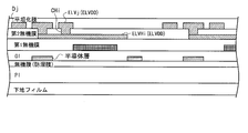
- FIG. 9 is a cross-sectional view taken along the line XX of FIG. 9 is a cross-sectional view taken along the line YY of FIG. It is a figure which shows the 2nd example of the layout pattern of the pixel circuit in the said 1st Embodiment.
- the gate terminal corresponds to the control terminal
- one of the drain terminal and the source terminal corresponds to the first conduction terminal
- the other corresponds to the second conduction terminal.
- the transistor in each embodiment is, for example, a thin film transistor, but the present invention is not limited thereto.
- connection means "electrical connection” unless otherwise specified, and is not limited to the case of direct connection without departing from the gist of the present invention, for example, a transistor. It also includes the case of meaning an indirect connection via another element such as.
- FIG. 1 is a block diagram showing an overall configuration of the organic EL display device 10a according to the first configuration example of the first embodiment.
- the display device 10a is an organic EL display device that performs internal compensation (details will be described later).
- the display device 10a includes a display unit 11, a display control circuit 20, a data side drive circuit 30, a scanning side drive circuit 40, and a power supply circuit 50.
- the data side drive circuit functions as a data signal line drive circuit (also called a "data driver”).
- the scanning side drive circuit 40 functions as a scanning signal line drive circuit (also referred to as a “gate driver”) and a light emission control circuit (also referred to as an “emission driver”).
- these two drive circuits are realized as one scanning side drive circuit 40, but these two drive circuits may be appropriately separated from each other, and these two drive circuits may be appropriately separated. May be separated and arranged on one side and the other side of the display unit 11.
- the power supply circuit 50 includes a high-level power supply voltage EL VDD, a low-level power supply voltage ELVSS, and an initialization voltage Vini to be supplied to the display unit 11, a display control circuit 20, a data side drive circuit 30, and a scanning side drive circuit 40. Generates a power supply voltage (not shown) to be supplied to.
- the display unit 11 is provided with M data signal lines D1 to DM (M is an integer of 2 or more) and N + 1 scanning signal lines G0 to GN intersecting them (N is an integer of 2 or more).
- N lines of light emission control lines (also referred to as "emission lines") E1 to EN are arranged along the N scanning signal lines G1 to GN, respectively.
- the display unit 11 is provided with M ⁇ N pixel circuits 15, and these M ⁇ N pixel circuits 15 have M data signal lines D1 to DM and N lines.
- Each pixel circuit 15 corresponds to any one of M data signal lines D1 to DM and is arranged in a matrix along the scanning signal lines G1 to GN.
- the pixel circuit corresponding to any one of the GNs (hereinafter, when each pixel circuit 15 is distinguished, the pixel circuit corresponding to the i-th scanning signal line Gi and the j-th data signal line Dj is referred to as "line i-th j". It is called a “column pixel circuit” and is indicated by the code “Pix (i, j)").
- the N light emission control lines E1 to EN correspond to the N scanning signal lines G1 to GN, respectively. Therefore, each pixel circuit 15 corresponds to any one of N light emission control lines E1 to EN.
- the extending direction of the scanning signal line Gi is referred to as the "row direction”
- the extending direction of the data signal line is referred to as the "column direction”.
- the display unit 11 is provided with a power line common to each pixel circuit 15. That is, the power supply line for supplying the high-level power supply voltage EL VDD for driving the organic EL element (hereinafter referred to as “high-level power supply line” or “first power supply voltage line”, and the same code as the high-level power supply voltage "EL appeal" (Indicated by) and a power supply line (hereinafter referred to as “low level power supply line” or “second power supply voltage line”, which is not shown) for supplying a low level power supply voltage ELVSS for driving an organic EL element, and is low level. Like the power supply voltage, the code "ELVSS" is arranged.
- the high-level power supply line EL VDD includes one main wiring ELV0 extending in the row direction and M trunk wiring ELV1 branching from the main wiring ELV0 and extending in the column direction (extending direction of the data signal line).
- the trunk wiring ELV1 to ELVN and the branch wiring ELVH1 to ELVHN have a one-to-one correspondence, but the number of trunk wiring is larger than the number of branch wiring, and each branch wiring ELVHi One or more trunk wiring ELVj may be electrically connected to each other.
- the connection between the trunk wiring ELVj and the branch wiring ELVHi shall mean an electrically conductive connection unless otherwise specified (the same applies to other embodiments).
- the "electrically conductive connection” refers to an electrical connection by a conductor to which the voltage drop can be ignored.
- the trunk wiring ELVj and the branch wiring ELVHi are formed in different wiring layers via an insulating layer, and the trunk wiring ELVj and the branch wiring ELVHi are connected to each other. (Electrical conduction connection) is realized by the contact hole CHi provided in the insulating layer (see FIGS. 10 and 11).
- the high-level power supply voltage EL VDD is supplied from the power supply circuit 50 to one end of the main wiring ELV0 of the power supply line. More specifically, in the main wiring ELV0, the position (hereinafter referred to as “feeding point”) PS where the high level power supply voltage EL VDD is supplied from the power supply circuit 50 is the first trunk wiring ELV1 from the main wiring ELV0 as shown in FIG. Is at or near the branching point.
- the distance from the main wiring ELV0 to each scanning signal line becomes longer in order from the first scanning signal line G1 to the Nth scanning signal line GN, so that the feeding point PS of the main wiring ELV0
- the closer to the trunk wiring ELVj the longer the distance from the main wiring ELV0 to the connection point CNi between the trunk wiring ELVj and the branch wiring ELVHi (that is, the length of the trunk wiring ELVj).
- the difference in the path length of the power supply line from the power supply circuit 50 to each pixel circuit 15 between the pixel circuits is suppressed.
- the branch wirings ELVH1 to ELVHN and the trunk wirings ELV1 to ELVM are formed in the display unit 11, and the main wiring ELV0 is a display in which the M ⁇ N pixel circuits 15 are arranged on the display panel (including the display unit 11). It is formed as wiring extending in the row direction in a frame area adjacent to the display unit 11 as an area (the same applies to other embodiments).
- Each pixel circuit 15 corresponds to any one of N branch wirings ELVH1 to ELVHN.
- Various signal lines, power supply lines, and thin film transistors (TFTs) described above are formed on the display unit 11 due to the layer structure (see FIGS. 10 and 11 described later).
- the display unit 11 has an initialization voltage supply line (same as the initialization voltage) (not shown) for supplying the initialization voltage Vini used for the reset operation for the initialization (details will be described later) of each pixel circuit 15. (Represented by "Vini") is also provided.
- the high level power supply voltage EL VDD, the low level power supply voltage ELVSS, and the initialization voltage Vini are supplied from the power supply circuit 50.
- the display control circuit 20 receives an input signal Sin including image information representing an image to be displayed and timing control information for displaying the image from the outside of the display device 10a, and based on this input signal Sin, the data side control signal Scd and scanning.
- the side control signal Scs is generated, the data side control signal Scd is sent to the data side drive circuit (data signal line drive circuit) 30, and the scanning side control signal Scs is sent to the scanning side drive circuit (scan signal line drive / light emission control circuit) 40. Output each.
- the data side drive circuit 30 drives the data signal lines D1 to DM based on the data side control signal Scd from the display control circuit 20. That is, the data side drive circuit 30 outputs M data signals D (1) to D (M) representing an image to be displayed in parallel to the data signal lines D1 to DM, respectively, based on the data side control signal Scd. Apply.
- the scanning side drive circuit 40 is a scanning signal line driving circuit that drives the scanning signal lines G0 to GN and a light emitting control circuit that drives the light emitting control lines E1 to EN based on the scanning side control signal Scs from the display control circuit 20. Functions as. More specifically, the scanning signal line driving circuit 40 sequentially selects scanning signal lines G0 to GM in each frame period based on the scanning signal line Scs as the scanning signal line driving circuit, and sets the selected scanning signal line Gk. On the other hand, an active signal (low level voltage) is applied, and an inactive signal (high level voltage) is applied to the non-selected scanning signal line.
- M pixel circuits Pix (n, 1) to Pix (n, M) corresponding to the selected scanning signal line Gn (1 ⁇ n ⁇ N) are collectively selected.
- M data signals D (1) to DM applied to the data signal lines D1 to DM from the data side drive circuit 30 during the selection period of the scanning signal line Gn (hereinafter, may be simply referred to as "data voltage” without distinguishing between these voltages) is used as pixel data in the pixel circuits Pix (n, 1) to Pix (n, M).
- data voltage (hereinafter, may be simply referred to as "data voltage” without distinguishing between these voltages) is used as pixel data in the pixel circuits Pix (n, 1) to Pix (n, M).
- the scanning side drive circuit 40 is a light emitting control that exhibits non-light emission with respect to the i-th light emitting control line Ei at least in the i-1 horizontal period and the i horizontal period based on the scanning side control signal Scs.
- a signal high level voltage
- a light emission control signal low level voltage
- the organic EL element in the pixel circuits Pix (i, 1) to Pix (i, M) corresponding to the i-th scanning signal line Gi has the light emission control line Ei while the voltage of the light emission control line Ei is at a low level.
- light is emitted with a brightness corresponding to the data voltage written in each of these pixel circuits Pix (i, 1) to Pix (i, M).
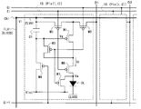
- FIG. 2 is a circuit diagram showing the configuration of the pixel circuit 15 in the present embodiment.
- FIG. 2 shows the configuration of the pixel circuit 15 corresponding to the i-th scanning signal line Gi and the first data signal line D1, that is, the pixel circuit Pix (i, 1) in the i-th row and the first column (1).
- ⁇ i ⁇ N The other pixel circuit 15 has a similar configuration.
- the configuration of the pixel circuit 15 in the present embodiment will be described by taking the pixel circuit Pix (i, 1) in the first row and the first column as an example.
- the M pixel circuits Pix (i, 1) to Pix (i, M) corresponding to the i-th scanning signal line Gi are referred to as "the i-th pixel circuit” or "i-th pixel circuit line”. That is.
- the pixel circuits Pix (i, 1) to Pix (i, M) constituting the i-th pixel circuit line are all connected to the i-th branch wiring ELVHi.
- the pixel circuit 15 includes an organic EL element OL as a display element, a drive transistor M1, a write control transistor M2, a threshold compensation transistor M3, a first initialization transistor M4, a first light emission control transistor M5, and a first light emission control transistor M5.
- the two emission control transistor M6, the second initialization transistor M7, and the holding capacitor C1 are included.
- transistors M2 to M7 other than the drive transistor M1 function as switching elements.
- the pixel circuit 15 includes a scanning signal line corresponding to the scanning signal line (hereinafter, also referred to as “corresponding scanning signal line” in the description focusing on the pixel circuit) Gi, and a scanning signal line immediately before the corresponding scanning signal line Gi (scanning signal lines G1 to G1 to It is the scanning signal line immediately before in the scanning order of GN, and is hereinafter also referred to as "preceding scanning signal line” in the description focusing on the pixel circuit) Gi-1, and the corresponding emission control line (hereinafter, the description focusing on the pixel circuit).
- corresponding light emission control line also referred to as "corresponding light emission control line”
- corresponding data signal line hereinafter, also referred to as “corresponding data signal line” in the description focusing on the pixel circuit
- initialization voltage supply line Vini high level power supply line.
- EL VDD and low level power supply line ELVSS are connected.
- the high-level power supply line EL VDD connected to the pixel circuit 15 is, more specifically, a branch wiring corresponding to the pixel circuit 15 among the N branch wirings ELVH1 to ELVHN included in the high-level power supply line EL VDD.
- the ELVHi (also referred to as “corresponding branch wiring”), that is, the i-th branch wiring (also referred to as “the branch wiring of the i-th row”) ELVHi.
- the i-th branch wiring ELVHi is connected to at least one trunk wiring ELVj of the trunk wirings ELV1 to ELVN branching from the main wiring ELV0. Therefore, a high level power supply voltage EL VDD is supplied to each pixel circuit 15 from the power supply circuit 50 via the main wiring ELV0, the trunk wiring ELVj, and the corresponding branch wiring ELVHi in this order.
- the source terminal as the first conduction terminal of the drive transistor M1 is connected to the corresponding data signal line Dj via the write control transistor M2, and the first light emission control transistor. It is connected to the high level power line EL VDD (more specifically, the corresponding branch wiring ELVHi) via M5.
- the drain terminal as the second conduction terminal of the drive transistor M1 is connected to the anode electrode of the organic EL element OL via the second light emission control transistor M6, and is connected to the low level power supply line ELVSS via the organic EL element OL.
- the gate terminal as the control terminal of the drive transistor M1 is connected to the high-level power supply line EL VDD (corresponding branch wiring ELVHi) via the holding capacitor C1, and the second drive transistor M1 is connected via the threshold compensation transistor M3. It is connected to the drain terminal as a conduction terminal and is connected to the initialization voltage supply line Vini via the first initialization transistor M4.
- the anode electrode of the organic EL element OL is connected to the initialization voltage supply line Vini via the second initialization transistor M7, and the cathode electrode of the organic EL element OL is connected to the low level power supply line ELVSS.
- the gate terminals of the write control transistor M2, the threshold compensation transistor M3, and the second initialization transistor M7 are connected to the corresponding scanning signal line Gi, and the gate terminals of the first and second light emission control transistors M5 and M6 are the corresponding light emission. It is connected to the control line Ei, and the gate terminal of the first initialization transistor M4 is connected to the preceding scanning signal line Gi-1.
- the drive transistor M1 operates in the saturation region, and the drive current Id flowing through the organic EL element OL during the light emission period is given by the following equation (1).
- the gain ⁇ of the drive transistor M1 included in the equation (1) is given by the following equation (2).
- Id ( ⁇ / 2) (
- ) 2 ( ⁇ / 2) (
- ⁇ ⁇ ⁇ (W / L) ⁇ Cox... (2)
- Vth, ⁇ , W, L, and Cox are the threshold voltage, mobility, gate width, gate length, and unit area of the drive transistor M1, respectively. Represents the gate insulating film capacity.
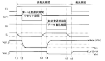
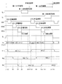
- FIG. 3 is a signal waveform diagram for explaining the driving of the display device according to the present embodiment, and is an initialization operation, a data writing operation, and a data writing operation of the pixel circuit Pix (i, j) in the i-th row and the j-th column.
- the voltage of each signal line (corresponding light emission control line Ei, preceding scanning signal line Gi-1, corresponding scanning signal line Gi, corresponding data signal line Dj) in the lighting operation, the voltage of the gate terminal of the drive transistor M1 (hereinafter referred to as "gate voltage").
- the change of Vg and the voltage (hereinafter referred to as “anode voltage”) Va of the anode electrode of the organic EL element OL is shown.
- anode voltage anode voltage
- the period from time t1 to t6 is the non-emission period of the pixel circuits Pix (i, 1) to Pix (i, M) in the i-th row.
- the period from time t2 to t4 is the i-1 horizontal period, and the period from time t2 to t3 is the selection period of the i-1th scanning signal line (preceding scanning signal line) Gi-1 (hereinafter, "i-1th"). Scanning selection period ").
- This i-1 scan selection period corresponds to the reset period of the pixel circuits Pix (i, 1) to Pix (i, M) in the i-th row.
- the period from time t4 to t6 is the i-horizontal period, and the period from time t4 to t5 is the selection period of the i-th scanning signal line (corresponding scanning signal line) Gi (hereinafter referred to as “i-scan selection period”). ..
- This i-scan selection period corresponds to the data writing period of the pixel circuits Pix (i, 1) to Pix (i, M) in the i-th row.
- the first and second light emission control transistors M5 and M6 change from the on state to the off state, and the organic EL element OL is in the non-light emitting state.
- the data of the data signal D (j) as the data voltage of the pixels of the i-1 row and column j by the data side drive circuit 30.
- the application to the signal line Dj is started, but in the pixel circuit Pix (i, j), the write control transistor M2 connected to the data signal line Dj is in the off state.
- the voltage of the preceding scanning signal line Gi-1 changes from a high level to a low level, so that the preceding scanning signal line Gi-1 is selected. Therefore, the first initialization transistor M4 changes to the ON state.
- the voltage at the gate terminal of the drive transistor M1 that is, the gate voltage Vg is initialized to the initialization voltage Vini.
- the initialization voltage Vini is a voltage sufficient to keep the drive transistor M1 in the ON state when the data voltage is written to the pixel circuit Pix (i, j). More specifically, the initialization voltage Vini satisfies the following equation (3).
- Vdata is the data voltage (voltage of the corresponding data signal line Dj)
- Vth is the threshold voltage of the drive transistor M1.
- the period from time t2 to t3 is the reset period in the pixel circuits Pix (i, 1) to Pix (i, M) in the i-th row, and in the pixel circuit Pix (i, j), as described above in this reset period.
- the gate voltage Vg is initialized when the first initialization transistor M4 is in the ON state.
- FIG. 3 shows a change in the gate voltage Vg (i, j) in the pixel circuit Pix (i, j) at this time.
- the code "Vg (i, j)" is used to distinguish the gate voltage Vg in the pixel circuit Pix (i, j) from the gate voltage Vg in other pixel circuits (the same applies hereinafter).
- the data-side drive circuit 30 shifts to the data signal line Dj of the data signal D (j) as the data voltage of the pixels in the i-th row and the j-th column. Is started, and the application of the data signal D (j) continues at least until the end time t5 of the i-th scan selection period.
- the write control transistor M2 changes to the ON state.
- the threshold value compensation transistor M3 also changes to the ON state, the drive transistor M1 is in a state in which its gate terminal and drain terminal are connected, that is, in a diode connection state.
- the voltage of the corresponding data signal line Dj that is, the voltage of the data signal D (j) is given to the holding capacitor C1 as the data voltage Vdata via the drive transistor M1 in the diode-connected state.
- the gate voltage Vg (i, j) changes toward the value given by the following equation (5).
- Vg (i, j) Vdata-
- the voltage of the corresponding scanning signal line Gi changes from a high level to a low level, so that the second initialization transistor M7 also changes to the ON state.
- the accumulated charge in the parasitic capacitance of the organic EL element OL is discharged, and the anode voltage Va of the organic EL element OL is initialized to the initialization voltage Vini (see FIG. 3).
- the reference numeral "Va (i, j)" is used to distinguish the anode voltage Va in the pixel circuit Pix (i, j) from the anode voltage Va in the other pixel circuits (the same applies hereinafter).
- the period from time t4 to t5 is the data writing period in the pixel circuits Pix (i, 1) to Pix (i, M) in the i-th row, and this data writing period in the pixel circuit Pix (i, j).
- the data voltage with the threshold compensation as described above is written in the holding capacitor C1, and the gate voltage Vg (i, j) becomes the value given by the above equation (5).
- the voltage of the light emission control line Ei changes to a low level.
- the first and second light emission control transistors M5 and M6 are changed to the ON state. Therefore, after time t6, the low-level power supply line ELVSS from the corresponding branch wiring ELVHi of the high-level power supply line EL VDD via the first light emission control transistor M5, the drive transistor M1, the second light emission control transistor M6, and the organic EL element OL.
- the current Id flows through. This current Id is given by the above equation (1).
- the drive transistor M1 is a P-channel type and EL VDD> Vg
- the current Id is given by the following equation from the above equations (1) and (5).
- the organic EL element OL emits light with brightness corresponding to the data voltage Vdata, which is the voltage of the corresponding data signal line Dj in the i-selective scanning period, regardless of the threshold voltage Vth of the drive transistor M1.
- the gate terminal of the drive transistor M1 is connected to the corresponding branch wiring ELVHi of the high-level power supply line EL VDD via the holding capacitor C1 and is connected to the source terminal of the drive transistor M1. Is connected to the corresponding branch wiring ELVHi of the high-level power supply line EL VDD via the first light emission control transistor M5, and the first light emission control transistor M5 is in the ON state during the light emission period.
- the i-th scan which is the data writing period of the pixel circuit 15 connected to the i-th scan signal line Gi and the j-th data signal line Dj, that is, the pixel circuit Pix (i, j) in the i-th row and the j-th column.
- the selection period when a current flows in the path of the power supply line from the power supply circuit 50 to the pixel circuit Pix (i, j), the voltage of the corresponding branch wiring ELVHi is actually high due to the voltage drop due to the current. The value is lower than the level power supply voltage VDD.
- the i-selective scanning period which is the data writing period of the pixel circuit Pix (i, j) in the i-th row and the j-th column
- the i-th emission control line Ei is set to a high level by the emission control circuit. Since it is in the (non-activated state), the pixel circuit 15 connected to the corresponding branch wiring ELVHi, that is, the pixel circuits Pix (i, 1) to Pix (i, M) in the i-th row are in the non-light emitting state.
- the pixel circuits Pix (i + 1,1) to Pix (i + 1, M) in the i + 1 row are also in a non-emission state because the i-th selective scanning period corresponds to their reset period.
- Pixel circuits Pix (p, 1) to Pix (p, M) (1 ⁇ p ⁇ N and p ⁇ i and p ⁇ i + 1) in rows other than these are in the light emitting state. Therefore, during the data writing period of the pixel circuit Pix (i, j) in the i-th row and the j-th column, no current flows through the corresponding branch wiring ELVHi in the i-th row, but the pixel circuit Pix in the light emitting state.
- the main wiring ELV0 and the path can be formed as wiring having a sufficiently low wiring resistance from the viewpoint of arrangement space as compared with the branch wirings ELVH1 to ELVHN and the trunk wirings ELV1 to ELVM arranged on the display unit 11. Therefore, it is possible to supply the high-level power supply voltage EL VDD with substantially no voltage drop from the corresponding branch wiring ELVHi to the pixel circuit Pix (i, j) in the i-th row and the j-th column during the data writing period.
- each pixel circuit 15 it is possible to supply each pixel circuit 15 with a high level power supply voltage EL VDD that has substantially no voltage drop from the corresponding branch wiring during the data writing period. Further, in this configuration example, it is not necessary to perform a circuit for compensating for a voltage drop due to a current in a power supply line such as a trunk wiring or a correction process for image data. Therefore, it is possible to suppress the deterioration of the display quality due to the luminance gradient or the like due to the voltage drop in the power supply line while avoiding the increase of the circuit or the like as much as possible.
- FIG. 4 is a block diagram showing the overall configuration of the organic EL display device 10b according to the second configuration example of the first embodiment.
- This display device 10b is different from the display device 10a according to the first configuration example in terms of the configuration of the power supply wiring (FIG. 1), but is the same as the display device 10a according to the first configuration example in other respects (FIG. 2). , See FIG. 3).
- the same or corresponding parts of the display device 10b according to the first configuration example will be designated by the same reference numerals as those of the display device 10a according to the first configuration example, and detailed description thereof will be omitted.
- the feeding point PS of the high level power supply voltage EL VDD from the power supply circuit 50 to the main wiring ELV0 is at or near the position where the first trunk wiring ELV1 branches from the main wiring ELV0.
- the distance from the main wiring ELV0 to the connection point CNi between the trunk wiring and the branch wiring increases in order from the first trunk wiring ELV1 to the Nth trunk wiring ELVN. That is, the connection point CNi between the trunk wiring ELVk and the branch wiring ELVHi is provided so as to be connected to the branch wiring ELVHi as far as the trunk wiring ELVk (1 ⁇ k ⁇ M) closer to the feeding point PS.
- a high level power supply voltage EL VDD is supplied from the power supply circuit 50 to both ends of the main wiring ELV0 in the power supply line. That is, the high-level power supply voltage EL VDD is supplied from the power supply circuit 50 to the two feeding points PS1 and PS2 in the main wiring ELV0, and the first main wiring ELV1 branches from the main wiring ELV0 at the first feeding point PS1.
- the second feeding point PS2 is located at or near the position, and the second main wiring ELV0 to the Nth trunk wiring ELVN (trunk wiring located at the end opposite to the end where the first trunk wiring is located) is located. It is at or near the branching position.
- the distance from the main wiring ELV0 to the connection point CNi between the trunk wiring and the branch wiring is gradually shortened from the trunk wirings ELV1 and ELVM at both ends toward the center in the row direction.
- the connection point CNi between the trunk wiring ELVk and the branch wiring ELVHi is provided so as to be connected to the branch wiring ELVHi as far as the trunk wiring ELVk closer to the feeding point (PS1 or PS2). It can be said that it is the same as the above-mentioned first configuration example in that it is.
- this configuration example as shown in FIG.
- the number of trunk wirings is equal to the number N of branch wirings, and only one trunk wiring ELVj is connected to each branch wiring ELVHi.
- the number M of the trunk wiring is made larger than the number N of the branch wiring (M> N), and one or more trunk wiring ELVj is connected to each branch wiring ELVHi. You may do so.
- one trunk wiring ELVk 1 to N
- the branch wiring ELVHi Only the branch wiring ELVHi is connected. From this, it is possible to supply the high level power supply voltage EL VDD to each pixel circuit 15 from the corresponding branch wiring with substantially no voltage drop during the data writing period, and the same effect as that of the first configuration example can be obtained. Be done. That is, also in this configuration example, it is possible to suppress the deterioration of the display quality due to the luminance gradient or the like due to the voltage drop in the power supply line while avoiding the increase of the circuit or the like as much as possible.
- FIG. 5 is a block diagram showing the overall configuration of the organic EL display device 10c according to the third configuration example of the first embodiment.
- This display device 10c is different from the display device 10a according to the first configuration example in terms of the configuration of the power supply wiring (FIG. 1), but is the same as the display device 10a according to the first configuration example in other respects (FIG. 2). , See FIG. 3).
- the same or corresponding parts of the display device 10c according to the first configuration example as those of the display device 10a according to the first configuration example will be designated by the same reference numerals, and detailed description thereof will be omitted.
- the high level power supply voltage EL VDD is supplied from the power supply circuit 50 to the power supply point PSm at the center position of the main wiring ELV0 in the power supply line.
- the feeding point PSm is a position where the central trunk wiring ELVm (there may be two central trunk wirings) of the M trunk wirings ELV1 to ELVM branches from the main wiring ELV0 or its vicinity.
- the distance from the main wiring ELV0 to the connection point CNi between the trunk wiring and the branch wiring is shortened from the central trunk wiring ELVm toward the trunk wirings at both ends.
- the configuration of the power supply line in this configuration example is that the connection point CNi between the trunk wiring and the branch wiring is provided so that the trunk wiring closer to the feeding point (PSm) is connected to the branch wiring farther away. , It can be said that it is the same as the above first configuration example. Also in this configuration example, as shown in FIG. 5, one or more trunk wiring ELVj is connected to each branch wiring ELVHi.
- FIG. 6 is a block diagram showing the overall configuration of the organic EL display device 10d according to the fourth configuration example of the first embodiment.
- This display device 10d is different from the display device 10a according to the first configuration example in terms of the configuration of the power supply wiring (FIG. 1), but is the same as the display device 10a according to the first configuration example in other respects (FIG. 2). , See FIG. 3).
- the same or corresponding parts of the display device 10d according to the first configuration example as those of the display device 10a according to the first configuration example will be designated by the same reference numerals, and detailed description thereof will be omitted.
- the high level power supply voltage EL VDD is supplied from the power supply circuit 50 to the feeding point PS1 located at one end of the main wiring ELV0 in the power supply line, as in the first configuration example. .. That is, the feeding point PS1 in this configuration example is at or near the position where the first trunk wiring ELV1 branches from the main wiring ELV0. Correspondingly, the distance from the main wiring ELV0 to the connection point CNi between the trunk wiring and the branch wiring becomes longer in order from the first trunk wiring ELV1 to the Mth trunk wiring ELVM, as in the first configuration example. It has become.
- each trunk wiring ELVj extends in the column direction from the main wiring ELV0 to the connection point CNi with the branch wiring ELVHi, and is shortened in order from the first trunk wiring ELV1 to the Mth trunk wiring ELVM. (The trunk wiring ELVj closer to the feeding point PS is longer), which is different from the first configuration example (see FIGS. 1 and 6).
- the trunk wiring ELV1 to ELVM all have the same length, the parasitic capacitance added to each scanning signal line Gi by the intersection of the scanning signal line Gi and the trunk wiring ELVj. Is the same value for all scanning signal lines Gi. That is, in this configuration example, the wiring capacitance in the scanning signal lines G1 to GN is made uniform as compared with the first configuration example, which is caused by the increase in the wiring capacitance of the scanning signal lines due to the arrangement of the trunk wiring ELV1 to ELVM. It is possible to suppress the deterioration of the display quality.
- FIG. 7 is a diagram schematically showing some suitable configuration examples of the power line in the present embodiment.
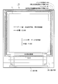
- FIG. 7A shows the configuration of the power line in the display device 10b according to the second configuration example shown in FIG. 4, and more specifically, the high level in the display panel (including the display unit 11) 100 in the display device 10b.
- the configuration of the power line is schematically shown.
- the display panel 100 includes a terminal unit 13 in addition to the display unit 11, and a high-level power supply voltage EL VDD is supplied from the power supply circuit 50 to the main wiring ELV0 via the terminal unit 13 (this point is shown in FIG. 7B).
- FIG. 7 (F) the high level power supply voltage EL VDD is supplied to both ends (feeding points PS1 and PS2) of the main wiring ELV0 via the terminal portion 13.
- each branch wiring (power line extending in the row direction) is connected to any one trunk wiring (power line extending in the column direction), and each trunk wiring is connected to any one branch wiring. It is connected.
- the distance from the main wiring ELV0 to the connection point CNi between the trunk wiring and the branch wiring is gradually shortened from the trunk wirings at both ends toward the center in the row direction.
- each trunk wiring is shortened in order from the trunk wiring at both ends toward the center in the row direction.
- the configuration example of the power supply line shown in FIG. 7B is basically the same as the configuration example of the power supply line shown in FIG. 7A, but the trunk wirings (power supply lines extending in the row direction) are connected to each other. It is connected to two adjacent branch wirings (power lines extending in the row direction), and this configuration example is different from the power line configuration example shown in FIG. 7A in this respect.
- a drive method that controls light emission in units of two rows of pixel circuits corresponding to two branch wirings connected to each trunk wiring, that is, the pixels of the two rows.
- FIG. 7 (A) shows.
- the same effect as the configuration example can be obtained. That is, even during the data writing period of the pixel circuit of any of the two rows, no current flows through the two branch wirings corresponding to the pixel circuits of the two rows, so that the two branch wirings are connected. No current flows through the trunk wiring, and no voltage drop occurs. Further, also in this configuration example, as in the configuration example of FIG.
- the distance from the main wiring ELV0 to the connection point CNi between the trunk wiring and the branch wiring is sequentially from the trunk wiring at both ends toward the center in the row direction. It is shortened, which suppresses the difference in the path length of the power supply line from the power supply circuit 50 to each pixel circuit between the pixel circuits.
- the drive method of FIG. 3 is adopted in this configuration example, in the data writing period of the pixel circuit of each row, another trunk wiring connected to the branch wiring corresponding to the pixel circuit of the row is used.
- the current to be supplied to the branch wiring may flow. However, even in this case, the current is a current supplied to one branch wiring, and the voltage drop due to the current is small.
- the configuration example of the power supply line shown in FIG. 7C is basically the same as the configuration example of the power supply line shown in FIG. 7B, but each trunk wiring (power supply line extending in the row direction) is one. It is connected to two adjacent branch wirings (power lines extending in the row direction) every other time, and this configuration example differs from the power line configuration example shown in FIG. 7B in this respect.
- a drive system suitable for this configuration example for example, two branch wirings connected to each trunk wiring and adjacent to each other are supported.
- the distance from the main wiring ELV0 to the connection point CNi between the trunk wiring and the branch wiring is the row direction from the trunk wiring at both ends. This is gradually shortened toward the center of the above, and this suppresses the difference in the path length of the power supply line from the power supply circuit 50 to each pixel circuit between the pixel circuits.
- the configuration example of the power supply line shown in FIG. 7 (D) has the same arrangement of the connection points between the trunk wiring and the branch wiring as the configuration example of the power supply line shown in FIG. 7 (A), but all the trunk wirings , It extends in the row direction so as to intersect any scanning signal line (and intersects any branch wiring) and has the same length. Therefore, the parasitic capacitance added to each scanning signal line due to the intersection of the scanning signal line and the trunk wiring has the same value for all the scanning signal lines. That is, in this configuration example, the wiring capacitance in the scanning signal line is made uniform as compared with the configuration example of FIG. 7A. In this configuration example as well, as in the configuration example of FIG. 7A, during the data writing period of the pixel circuit of each row, not only the branch wiring connected to the pixel circuit of the row but also the branch wiring is connected. Even in the trunk wiring, no current flows and no voltage drop occurs.
- FIG. 7 (E) schematically shows the configuration of a power supply line (high level power supply line) in the display panel (including the display unit 11) in the display device 10c according to the third configuration example shown in FIG. ..
- the high level power supply voltage EL VDD is supplied to the center of the main wiring ELV0 via the terminal portion 13.
- each branch wiring power line extending in the row direction
- each trunk wiring is connected to any one branch wiring. It is connected.
- each trunk wiring branches from the main wiring ELV0 and extends to the connection point with the branch wiring, each trunk wiring becomes longer in order from the trunk wiring at both ends toward the center in the row direction.
- FIG. 7F shows a configuration example in which the number M of the trunk wiring is larger than the number N of the branch wiring.
- a high level power supply voltage EL VDD is supplied to both ends of the main wiring ELV0 via the terminal portion 13.
- the number M of the trunk wiring is larger than the number N of the branch wiring, so that the upper branch wiring (branch wiring far from the main wiring ELV0) is in the center.
- the lower branch wiring (branch wiring close to the main wiring ELV0) is connected to the one trunk wiring arranged near the center. Has been done.
- each branch wiring is connected to one or two trunk wirings, and each trunk wiring is connected to only one of the branch wirings.
- the distance from the main wiring ELV0 to the connection point CNi between the trunk wiring and the branch wiring is gradually shortened from the trunk wirings at both ends toward the center in the row direction.
- the difference in the path length of the power supply line from the power supply circuit 50 to each pixel circuit between the pixel circuits is suppressed. Since the distance from the main wiring ELV0 to the branch wiring to which the trunk wiring near the center should be connected is short, the voltage drop does not become a problem even if there is only one trunk wiring connected to the branch wiring. ..
- the pixel is in the data writing period of each pixel circuit. Not only does the branch wiring connected to the circuit (corresponding branch wiring) not allow current to flow and no voltage drop occurs, but also the trunk wiring connected to the branch wiring does not allow current to flow and cause a voltage drop. Can be done. Further, as described above, the routes from the main wiring ELV0 and the power supply circuit 50 to the main wiring ELV0 through the terminal portion 13 of the power supply lines are arranged as compared with the branch wiring and the trunk wiring arranged in the display unit 11. From the viewpoint of space, it can be formed as a wiring having a sufficiently low wiring resistance.
- the wiring capacity of the scanning signal line is made uniform as compared with the other configuration examples, so that the wiring capacity of the scanning signal line can be increased by arranging the trunk wiring. It is possible to suppress the deterioration of display quality caused by this.
- pixel circuit layout pattern a layout pattern for realizing the pixel circuit 15 (FIG. 2) in the present embodiment
- pixel circuit layout pattern a layout pattern for realizing the pixel circuit 15 (FIG. 2) in the present embodiment
- a circuit to be formed on the display unit 11 that is, a pixel circuit arranged in a matrix
- a layout pattern for realizing a circuit consisting of a power line or the like hereinafter referred to as “display unit layout pattern”.
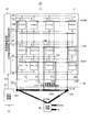
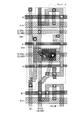
- FIG. 8 is a diagram showing a first example of a layout pattern of the pixel circuit Pix (i, j) in the i-th row and the j-th column in the present embodiment (see FIG. 2).
- a pattern with hatched diagonal lines extending in the column direction indicates a wiring pattern formed of a metal material in a certain layer, and the diagonal lines extend in the row direction (horizontal direction in the figure).
- the hatched pattern shows a wiring pattern made of a metal material in the other layer, and the hatched pattern of the lattice extending in the row direction shows the wiring made of a metal material in the other layer.
- the pattern (wiring pattern of the gate line as the scanning signal line) is shown, and the pattern with the hatched dots shows the wiring pattern formed of the semiconductor material in the other layer (FIGS. 10 and 10 described later). 11). Further, a circle consisting of two semicircles with different hatchings indicates a contact hole, and the hatching attached to each of the two semicircles is the wiring pattern indicated by the hatching of one semicircle and the other. It shows that the wiring pattern shown by the hatching of the semicircle is electrically conducted and connected by the contact hole.
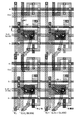
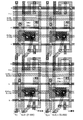
- FIG. 9 is a diagram showing a first example of a layout pattern of a display unit using the layout pattern of the pixel circuit Pix (i, j) shown in FIG.
- the layout pattern of this display unit corresponds to the configuration of the power supply line shown in FIG. 1, and M trunk wirings ELV1 to ELVM are arranged along the M data signal lines D1 to DM, respectively.
- M trunk wirings ELV1 to ELVM are arranged along the M data signal lines D1 to DM, respectively.
- Only one branch wiring ELVHi is connected to each trunk wiring ELVj.
- the number M of the trunk wiring ELV1 to ELVM (this is equal to the number of data signal lines) is the number N of the branch wiring ELVH1 to ELVHN (this is the number of scanning signal lines G1 to GN and the number of light emission control lines E1 to EN). Since there are more than (M> N), there are places (not shown) where two or more trunk wires ELVj1, ELVj2, ... Are connected to
- FIG. 10 is a cross-sectional view taken along the line XX of FIG. 9, and FIG. 11 is a cross-sectional view taken along the line YY of FIG.
- the trunk wiring ELVj and the branch wiring ELVHi are formed in different wiring layers via an insulating layer, and the trunk wiring ELVj and the branch wiring ELVHi are connected (electrically).
- Conductive connection) is realized by the contact hole CHi provided in the insulating layer. That is, the connection point CNi between the trunk wiring ELVj and the branch wiring ELVHi shown in FIGS. 1 and 2, is realized by the contact holes CHi shown in FIGS. 8 to 11.
- the circuit of the display unit 11 including the power supply lines (trunk wiring and branch wiring) having the configuration shown in FIG. 1 can be realized as a device having the structure shown in FIGS. 8 to 11. Further, as is clear from FIGS. 8 to 11 (particularly the cross-sectional views shown in FIGS. 10 and 11), the circuit of the display unit 11 including the power supply lines having other configurations shown in FIGS. 4 to 7 has the same structure. It can be realized as a device of.
- FIG. 12 is a diagram showing a second example of the layout pattern of the pixel circuit Pix (i, j) of the i-th row and the j-th column in the present embodiment (see FIG. 2), and FIG. 13 is shown in FIG. It is a figure which shows the 2nd example of the layout pattern of the display part using the layout pattern of a pixel circuit Pix (i, j).
- the layout pattern of this display unit also corresponds to the configuration of the power line shown in FIG.
- one branch wiring ELVHi in the configuration shown in FIG. 1 is realized by two wiring patterns ELVHai and ELVHbi, and correspondingly, the trunk wiring ELVj and the branch wiring
- the connection point CNi with ELVHi is realized by two contact holes CHai and CHbi.
- the circuit of the display unit 11 including the configuration of the power line shown in FIG. 1 can be realized.
- the circuit of the display unit 11 including the power supply lines having other configurations shown in FIGS. 4 to 7 is also a second example. It can be realized by using the same layout pattern as the layout pattern by.
- SSD Source Shared Driving
- FIG. 14 is a block diagram showing an overall configuration of the display device 10e according to the present embodiment.
- the display device 10e is an organic EL display device that performs internal compensation as in the first embodiment, but differs from the first embodiment in that an SSD method having a multiplicity of 3 is adopted. ..
- the display device 10e performs color display using the three primary colors of red, green, and blue, and sets the three data signal lines corresponding to the three primary colors as one set and divides the three data signal lines in each set into time divisions.
- the SSD method driven by is adopted. Since the configuration of the present embodiment is the same as that of the first embodiment except for the configuration relating to these points, the same or corresponding parts are designated by the same reference numerals and detailed description thereof will be omitted.
- the display device 10e includes a display unit 11, a display control circuit 20, a data signal line drive circuit 30, and a scanning side drive circuit 40 that functions as a scanning signal line drive and light emission control circuit. It also includes a power supply circuit 50.
- the display unit 11 includes three data signal lines consisting of R data signal lines Drj, G data signal lines Dgj, and B data signal lines Dbj corresponding to red, green, and blue, which form the three primary colors, as a set.
- Data signal lines Dr1, Dg1, Db1 to DrM, DgM, DbM of M group (3M lines) and N + 1 scanning signal lines G0 to GN intersecting these are arranged.
- N light emission control lines E1 to EN are arranged along the N scanning signal lines G1 to GN, respectively.
- N scanning signals are arranged along the line.
- lines G1 to GN corresponds to any one of lines G1 to GN.
- the pixel circuit corresponding to the i-th scanning signal line Gi and the j-th group R data signal line Drj is referred to as "i-line j-th group R pixel circuit".
- the pixel circuit represented by the reference numeral “Pr (i, j)” and corresponding to the i-th scanning signal line Gi and the j-th set G data signal line Dgj is referred to as “i-line j-th set G pixel circuit” and has a reference numeral.
- the pixel circuit indicated by “Pg (i, j)” and corresponding to the i-th scanning signal line Gi and the j-th set B data signal line Dbj is referred to as "i-line j-th set B pixel circuit" and has a reference numeral ". It shall be indicated by "Pb (i, j)".
- the light emission control lines E1 to EN of the book are connected to the scanning side drive circuit (scanning signal line drive / light emission control circuit) 40 as in the first embodiment.
- the display unit 11 has a high-level power supply line for supplying a high-level power supply voltage EL VDD as a power supply line common to each pixel circuit 15 (the same code as the high-level power supply voltage EL VDD). (Represented by) and a power supply line for supplying the low-level power supply voltage ELVSS (represented by the symbol ELVSS in the same manner as the low-level power supply voltage) are arranged.
- the power line in this embodiment is configured in the same manner as the second configuration example in the first embodiment shown in FIG. That is, as shown in FIG.
- the high-level power supply line EL VDD includes one main wiring ELV0 extending in the row direction, N main wirings ELV1 to ELVN branching from the main wiring ELV0 and extending in the column direction, and a scanning signal. Includes N branch wirings ELVH1 to ELVHN arranged along the lines G1 to GN, respectively.
- the number of trunk wirings is equal to the number of branch wirings, but the number of trunk wirings (for example, 3 ⁇ M trunk wirings) may be larger than the number of branch wirings. In this case, a configuration in which two or more trunk wires are connected to one branch wire is included (see FIG. 7 (F)).
- the high-level power supply voltage EL VDD is supplied from the power supply circuit 50 to the feeding points PS1 and PS2 located at both ends of the main wiring ELV0 of the power supply line.
- the first feeding point PS1 is at or near the position where the first trunk wiring ELV1 branches from the main wiring ELV0
- the second feeding point PS2 is from the main wiring ELV0 to N.
- the distance from the main wiring ELV0 to the connection point CNi between the trunk wiring and the branch wiring is gradually shortened from the trunk wirings ELV1 and ELVM at both ends toward the center in the row direction. That is, the connection point CNi between the trunk wiring ELVj and the branch wiring ELVHi is provided so that the trunk wiring ELVk closer to the feeding point (PS1 or PS2) is connected to the branch wiring ELVHi.
- the display control circuit 20 receives the input signal Sin from the outside of the display device 10e, generates the data side control signal Scd and the scanning side control signal Scs based on the input signal Sin, and generates the data side control signal Scd and the scanning side control signal Scs.
- the control signal Scd is output to the data side drive circuit 30a in the data signal line drive circuit 30, and the scanning side control signal Scs is output to the scanning side drive circuit 40.
- the display control circuit 20 outputs the R selection control signal SSDr, the G selection control signal SSDg, and the B selection control signal SSDb to the demultiplex circuit 30b in the data signal line drive circuit 30.
- the data signal line drive circuit 30 includes a data side drive circuit 30a and a demultiplex circuit 30b.
- the data side drive circuit 30a has the same configuration as the data side drive circuit 30 in the first embodiment, and has M output terminals Ta1 to TaM. However, since the SSD method having a multiplicity of 3 is adopted in the present embodiment as described above, the data side drive circuit 30a functions as a time division data signal generation circuit. That is, the data side drive circuit 30a is based on the data side control signal Scd from the display control circuit 20, and the R data signal Dr (j) and the G data signal line to be applied to the R data signal line Drj in each horizontal period.
- the R data signal Dr (j) includes pixel data to be written in the R pixel circuit Pr (i, j) of the i-row j-th group
- the G data signal Dg (j) is the i-line j
- the B data signal Db (j) includes the pixel data to be written to the G pixel circuit Pg (i, j) of the i-row j group
- the R selection control signal SSDr, the G selection control signal SSDg, and the B selection control signal SSDb output from the display control circuit 20 are given to all the demultiplexers 31 to 3M.
- the input side of the j-th demultiplexer 3j is connected to the j-th output terminal Taj in the data-side drive circuit 30a, and the output side is connected to the three data signal lines Drj, Dgj, and Dbj of the j-th group.
- FIG. 15 is a diagram for explaining a layout configuration in the present embodiment adopting the SSD method.
- the display panel includes a display unit 11 in which pixel circuits are arranged in a matrix and a terminal unit 13 for receiving a signal or a power supply voltage from the outside, and in addition, the side of the display unit 11
- the SSD area R14 is provided around the display unit along the side closest to the terminal unit 13.
- the demultiplex circuit 30b is integrally formed in the same process as the pixel circuit in the display unit 11.
- a main wiring ELV0 in the power supply line is formed between the SSD region R14 and the terminal portion 13 along the SSD region R14, and a high-level power supply is supplied from the external power supply circuit 50 to the main wiring via the terminal portion 13.
- the voltage EL VDD is supplied.
- a high level power supply voltage EL VDD is supplied to both ends of the main wiring ELV0.
- a region R41 for a scanning signal line drive circuit is provided in the peripheral portion of the display unit 11 along two opposite sides other than the side along the SSD region R14 and the side facing the SSD region R14 among the sides of the display unit 11.
- a trench RT is formed on the outside thereof so as to be in contact with the region R41 and surround the three sides of the display unit 11.
- a region R42 for a light emission control circuit is provided outside the trench RT in contact with the trench RT and along the region R41.
- a bank area R50 for a control circuit is provided outside the area R42 so as to be in contact with the area R42 and surround the three sides of the display unit 11, and the bank area R50 is connected to the terminal unit 13. Includes the area of.
- the high-level power supply voltage EL VDD is supplied from the external power supply circuit 50 to the main wiring ELV0 via the terminal portion 13, and as shown in FIG. 14, the main wiring ELV0 is further supplied. It is supplied to each pixel circuit via each trunk wiring ELVj branching from and branch wiring ELVHi connected to each trunk wiring ELVj (not shown in FIG. 15).
- FIG. 16 is a signal waveform diagram for explaining the driving of the display device 10e according to the present embodiment, and is a signal waveform diagram of the three pixel circuits Pr (i, j), Pg (i, j), in the i-row j-th group. The change of each signal in the initialization and the pixel data writing in Pb (i, j) is shown.
- the period from time t1 to t7 is the i-1 horizontal period, and the period from time t5 to t6 is the selection period of the i-1th scan signal line Gi-1, that is, the i-1 scan selection period.
- the period from time t7 to t13 is the i-th horizontal period, and the period from time t11 to t12 is the selection period of the i-th scanning signal line Gi, that is, the i-th scanning selection period.
- the R selection control signal SSDr and the G selection control signal SSDg are in a period prior to the start time of the scanning selection period (hereinafter referred to as “pre-selection period”).
- the R selection control signal SSDr and the G selection control signal SSDg are sequentially generated in conjunction with the B selection control signal SSDb. It is output.
- the voltages of the R data signal dr (i-1, j), the G data signal deg (i-1, j), and the B data signal db (i-1, j) that are sequentially output are the demultiplexer 3j.
- the formed wiring capacity is referred to as "data line capacity Cdxj"). That is, in the pre-selection period (t1 to t5), during the period when the R selection control signal SSDr is at a low level (hereinafter referred to as “R line charging period”), the R data signal is the voltage of the R data signal dr (i-1, j).
- the voltage of the G data signal dc (i-1, j) is used.
- the B data signal db (i-1, i) is charged by the voltage of. As shown in FIG.
- the voltage of the R data signal line Drj at the end of the R line charging period the voltage of the G data signal line Dgj at the end of the G line charging period, and B at the end of the B line charging period.
- the voltage of the data signal line Dbj is held at least during the scan selection period (t5 to t6) within the horizontal period.
- the voltage Vg of the gate terminal of the drive transistor M1 is initialized to the initialization voltage Vini.
- the R selection control signal SSDr, the G selection control signal SSDg, and the B selection control signal SSDb are each for a predetermined period.
- the R selection control signal SSDr, the G selection control signal SSDg, and the B selection control are transmitted from the output terminal Tar of the data side drive circuit 30a as shown in FIG.
- the R data signal dr (i, j), the G data signal DG (i, j), and the B data signal db (i, j) are sequentially output in conjunction with the signal SSDb.
- the voltages of the R data signal dr (i, j), the G data signal deg (i, j), and the B data signal db (i, j) that are sequentially output are determined by the data signal line Drj, by the demultiplexer 3j.
- the data line capacitance Cdrj which is the wiring capacitance of the R data signal line Drj, is charged by the voltage of the R data signal dr (i, j), and G
- the voltage of the G data signal dc (i, j) charges the data line capacity Cdegj, which is the wiring capacity of the G data signal line Dgj, and in the B line charging period, the voltage of the B data signal db (i, j).
- the data line capacity Cdbj which is the wiring capacity of the B data signal line Dbj, is charged.
- the voltage of the R data signal line Drj at the end of the R line charging period, the voltage of the G data signal line Dgj at the end of the G line charging period, and the voltage of the B data signal line Dbj at the end of the B line charging period are , At least during the scan selection period (t11 to t12) within the horizontal period.
- the voltage of the R data signal line Drj that is, the voltage of the R data signal dr (i, j) held in the data line capacitance Cdrj is the R of the i-line j-th set.
- the voltage of the G data signal line Dgj written as pixel data in the pixel circuit Pr (i, j), that is, the voltage of the G data signal df (i, j) held in the data line capacitance Cdgj is the i-line j-th set.
- the voltage of the B data signal line Dbj written as pixel data in the G pixel circuit Pg (i, j), that is, the voltage of the B data signal db (i, j) held in the data line capacitance Cdbj is the i-line j-th set. It is written as pixel data in the B pixel circuit Pb (i, j) of.
- each trunk wiring ELVj is connected to only one branch wiring ELVHi, whereby the branch wiring connected to the pixel circuit of the row concerned is connected during the data writing period of the pixel circuit of each row. Not only in the trunk wiring connected to the branch wiring, no current flows and no voltage drop occurs.
- the routes from the main wiring ELV0 and the power supply circuit 50 to the main wiring ELV0 via the terminal portion 13 of the power supply lines are the branch wiring and the trunk wiring arranged in the display unit 11.
- the number of trunk wirings is equal to the number M of data signal lines and larger than the number N of branch wirings (M>. N)
- the number of trunk wirings is equal to, but not limited to, the number N of branch wirings. That is, in any of the first to fourth configuration examples, the number of trunk wirings may be equal to or greater than the number of branch wirings. In this way, at least one trunk wiring can be connected to each branch wiring, and only one branch wiring can be connected to each trunk wiring.
- the number of trunk wirings may be 1 ⁇ 2 or more of the number of branch wirings. ..
- the power supply line (high level power supply line) is configured so that each trunk wiring is connected to one or two branch wirings, but each trunk wiring is displayed.
- the configuration may be such that it is connected to only a part of the N branch wirings in the unit 11.
- the main wiring ELV0 in the power supply line is one wiring provided in the frame area around the display unit 11 and extending in the row direction.
- the main wiring ELV0 is the frame area.
- two or more power supply wirings extending in the row direction may be formed.
- the main wiring ELV0 is preferably formed of the same metal material in the same layer as the plurality of trunk wirings ELV1 to ELVM (or ELV1 to ELVN) branched from the main wiring ELV0.
- the pixel circuit as shown in FIG. 2 corresponding to the internal compensation method is used, but the configuration of the pixel circuit is not limited to this.
- One end of the holding capacitor C1 is connected to the gate terminal of the driving transistor M1, the other end of the holding capacitor C1 and the source terminal of the driving transistor M1 are connected to the corresponding branch wiring ELVi, and a current flows through the organic EL element during the data writing period.
- a pixel circuit having another configuration may be used.
- an SSD method having a multiplicity of 3 is adopted, but the multiplicity of the SSD method is not limited to this, and an SSD having a multiplicity of 2 or 4 or more.
- the present invention can also be applied to a display device that employs the method.
- an embodiment and a modification thereof have been described by taking an organic EL display device as an example, but the present invention is not limited to the organic EL display device, and uses a display element driven by an electric current. It can be applied to any display device that has been used.
- the display element that can be used here is a display element whose brightness or transmission rate is controlled by a current, and is, for example, an organic EL element, that is, an organic light emitting diode (OLED), an inorganic light emitting diode, or the like.
- OLED organic light emitting diode
- QLED Quantum dot Light Emitting Diode
Landscapes
- Engineering & Computer Science (AREA)
- Physics & Mathematics (AREA)
- General Physics & Mathematics (AREA)
- Theoretical Computer Science (AREA)
- Computer Hardware Design (AREA)
- Microelectronics & Electronic Packaging (AREA)
- Electroluminescent Light Sources (AREA)
- Devices For Indicating Variable Information By Combining Individual Elements (AREA)
- Control Of Indicators Other Than Cathode Ray Tubes (AREA)
- Control Of El Displays (AREA)
Abstract
本願は、回路の増大をできるだけ回避しつつ、電源線での電圧降下に起因する輝度傾斜等による表示品質の低下を抑制できる電流駆動型表示装置を開示する。有機EL表示装置において、ハイレベル電源線ELVDDは、主配線ELV0と、主配線ELV0から分岐して列方向に延びる幹配線ELV1~ELVMと、走査信号線G1~GNに沿って行方向に延びる枝配線ELVH1~ELVHN0とを含む。幹配線と枝配線とは絶縁層を介して互いに異なる層にそれぞれ形成されており、各枝配線は少なくとも1つの幹配線とコンタクトホールにより電気的に導通接続され、かつ、各幹配線は1つの枝配線のみとコンタクトホールにより電気的に導通接続されている。各画素回路はそのデータ書込期間に電流が流れないように構成されており、当該書込期間では対応枝配線および対応枝配線に接続された幹配線において電圧降下が生じない。
Description
本発明は表示装置に関し、より詳しくは、有機EL(Electro Luminescence)表示装置等の電流で駆動される表示素子を備えた電流駆動型の表示装置に関する。
近年、有機EL素子(有機発光ダイオード(Organic Light Emitting Diode: OLED)とも呼ばれる)を含む画素回路を備えた有機EL表示装置が実用化されている。有機EL表示装置の画素回路は、有機EL素子に加えて、駆動トランジスタや、書込制御トランジスタ、保持キャパシタ等を含んでいる。駆動トランジスタや書込制御トランジスタには、薄膜トランジスタ(Thin Film Transistor)が使用され、駆動トランジスタの制御端子としてのゲート端子に保持キャパシタが接続され、この保持キャパシタには、駆動回路からデータ信号線を介して、表示すべき画像を表す映像信号に応じた電圧(より詳しくは当該画素回路で形成すべき画素の階調値を示す電圧であり、以下「データ電圧」という)が与えられる。有機EL素子は、それに流れる電流に応じた輝度で発光する自発光型表示素子である。駆動トランジスタは、有機EL素子と直列に設けられ、保持キャパシタに保持される電圧にしたがって、有機EL素子に流れる電流を制御する。
有機EL表示装置の表示部には、複数の画素回路がマトリクス状に配置されており、各画素回路における有機EL素子に電流を供給するために電源線が配設されている。電源線は配線抵抗を有しているので、それに接続された画素回路内の有機EL素子に供給される電流により当該電源線において電圧降下が生じ、各画素回路の保持キャパシタに保持される電圧はその電圧降下の影響を受ける。このため、各画素回路に同じデータ電圧を与えても、保持キャパシタに保持される電圧が若干相違し、表示部における位置によって表示輝度が多少異なる。これは表示画像における輝度傾斜として視認されることがあり、このような輝度傾斜が現れる現象は「シェーディング現象」とも呼ばれる。
これに対し特許文献1には、画素回路内の容量素子(保持キャパシタ)へのデータ電圧の書込期間において当該画素回路に電流が流れ込まず、複数の電源線が複数のデータ線に交差し複数の走査線に沿って配置されるように構成された発光装置が開示されている(段落[0028]、[0029]、[0033])。この構成によれば、電源線に流れる電流による電圧降下で画素回路内の容量素子(保持キャパシタ)への書込電圧が影響されるという現象が抑えられる(段落[0033]~[0034])。また特許文献2には、マトリクス状に配置された画素毎に電流駆動型の自発光素子を備えたアクティブマトリクス型表示装置において、画素へのデータ書き込みの際の電圧降下を最低限に抑制するために、書込対象の行に沿った水平PVDDライン(水平電源ライン)に電源を供給する垂直PVDDライン(垂直電源ライン)と、他の行の水平PVDDラインに電源を供給する垂直PVDDラインとが異なるようにした構成が開示されている(段落[0031]~[0034]等)。
しかし、特許文献1に開示された上記構成では、複数の走査線に沿って配置された複数の電源線に電源回路から電源電圧を供給するために配置された主電源線において電圧降下が生じ、それにより画素回路の保持キャパシタへの書込電圧が影響を受ける。また、特許文献2に開示された上記構成では、選択されるゲートライン(走査信号線)の切替に応じて、水平PDVVラインが接続される垂直PVDDラインを切り替えるための回路が別途、必要となる(段落[0033]~[0034])。また特許文献2には、水平PDVVラインでの電圧降下の書込電圧への影響を抑えるための構成についての具体的な記載が見られない。
そこで、有機EL表示装置のような電流駆動型表示装置において、回路の増大をできるだけ回避しつつ、電源線での電圧降下に起因する輝度傾斜等による表示品質の低下を抑えることが望まれる。
本発明の幾つかの実施形態に係る表示装置は、
行方向に延びる複数の走査信号線と、列方向に延び前記複数の走査信号線に交差する複数のデータ信号線と、前記複数の走査信号線および前記複数のデータ信号線に沿ってマトリクス状に配置された複数の画素回路とが設けられた表示部を有する表示装置であって、
第1および第2電源電圧線を含む電源線と、
前記複数のデータ信号線を駆動するデータ信号線駆動回路と、
前記複数の走査信号線を選択的に駆動する走査信号線駆動回路と
を備え、
前記第1電源電圧線は、
前記表示部に隣接する額縁領域に設けられ行方向に延びる主配線と、
前記主配線から分岐して列方向に延びる複数の幹配線と、
前記複数の走査信号線にそれぞれ沿って配設される複数の枝配線とを含み、
各画素回路は、
前記複数の走査信号線のいずれか1つに対応し、かつ、前記複数のデータ信号線のいずれか1つに対応し、かつ、前記複数の枝配線のいずれか1つに対応し、
電流によって駆動される表示素子と、前記表示素子の駆動電流を制御するためのデータ電圧を保持する保持キャパシタと、前記保持キャパシタに保持されたデータ電圧に応じて前記表示素子の駆動電流を制御する駆動トランジスタとを含み、
各画素回路において、前記駆動トランジスタの第1導通端子は当該画素回路に対応する枝配線に接続され、前記駆動トランジスタの第2導通端子は前記表示素子を介して前記第2電源電圧線に接続され、前記駆動トランジスタの制御端子は前記保持キャパシタを介して前記対応する枝配線に接続されており、
前記表示部は、
前記複数の枝配線が形成された配線層と、
前記複数の幹配線が形成された配線層と、
前記複数の枝配線と前記複数の幹配線とに挟まれた絶縁層と、
前記複数の枝配線のそれぞれが前記複数の幹配線のうち少なくとも1つの幹配線と電気的に導通接続されるとともに前記複数の幹配線のそれぞれが前記複数の枝配線のうち一部の枝配線のみと電気的に導通接続されるように、前記絶縁層に設けられたコンタクトホールとを含む。
行方向に延びる複数の走査信号線と、列方向に延び前記複数の走査信号線に交差する複数のデータ信号線と、前記複数の走査信号線および前記複数のデータ信号線に沿ってマトリクス状に配置された複数の画素回路とが設けられた表示部を有する表示装置であって、
第1および第2電源電圧線を含む電源線と、
前記複数のデータ信号線を駆動するデータ信号線駆動回路と、
前記複数の走査信号線を選択的に駆動する走査信号線駆動回路と
を備え、
前記第1電源電圧線は、
前記表示部に隣接する額縁領域に設けられ行方向に延びる主配線と、
前記主配線から分岐して列方向に延びる複数の幹配線と、
前記複数の走査信号線にそれぞれ沿って配設される複数の枝配線とを含み、
各画素回路は、
前記複数の走査信号線のいずれか1つに対応し、かつ、前記複数のデータ信号線のいずれか1つに対応し、かつ、前記複数の枝配線のいずれか1つに対応し、
電流によって駆動される表示素子と、前記表示素子の駆動電流を制御するためのデータ電圧を保持する保持キャパシタと、前記保持キャパシタに保持されたデータ電圧に応じて前記表示素子の駆動電流を制御する駆動トランジスタとを含み、
各画素回路において、前記駆動トランジスタの第1導通端子は当該画素回路に対応する枝配線に接続され、前記駆動トランジスタの第2導通端子は前記表示素子を介して前記第2電源電圧線に接続され、前記駆動トランジスタの制御端子は前記保持キャパシタを介して前記対応する枝配線に接続されており、
前記表示部は、
前記複数の枝配線が形成された配線層と、
前記複数の幹配線が形成された配線層と、
前記複数の枝配線と前記複数の幹配線とに挟まれた絶縁層と、
前記複数の枝配線のそれぞれが前記複数の幹配線のうち少なくとも1つの幹配線と電気的に導通接続されるとともに前記複数の幹配線のそれぞれが前記複数の枝配線のうち一部の枝配線のみと電気的に導通接続されるように、前記絶縁層に設けられたコンタクトホールとを含む。
本発明の上記幾つかの実施形態では、第1電源電圧線は、表示部に隣接する額縁領域に設けられ行方向(走査信号線の延伸方向)に延びる主配線と、当該主配線から分岐して列方向(データ信号線の延伸方向)に延びる複数の幹配線と、当該複数の走査信号線にそれぞれ沿って配設される複数の枝配線とを含み、当該複数の枝配線のそれぞれが当該複数の幹配線のうち少なくとも1つの幹配線と電気的に導通接続されるとともに当該複数の幹配線のそれぞれが当該複数の枝配線のうち一部の枝配線のみと電気的に導通接続されるように構成されている。このため、各画素回路をそのデータ電圧の書込期間において電流が流れない構成とすることにより、データ電圧を書き込むべき画素回路に接続される枝配線に電流が流れないだけでなく、当該枝配線に接続される幹配線においても電流が流れないか、電流が流れても従来に比べ当該電流の量は大きく削減される。その結果、各画素回路にデータ電圧を書き込むときに当該画素回路に第1電源電圧線によって供給される電源電圧の低下を従来よりも大きく抑制することができる。したがって、本発明の上記幾つかの実施形態によれば、回路の増大をできるだけ回避しつつ、電源線での電圧降下に起因する輝度傾斜等による表示品質の低下を抑えることができる。
以下、添付図面を参照しながら各実施形態について説明する。なお、以下で言及する各トランジスタにおいて、ゲート端子は制御端子に相当し、ドレイン端子およびソース端子の一方は第1導通端子に相当し、他方は第2導通端子に相当する。また、各実施形態におけるトランジスタはすべてPチャネル型であるものとして説明するが、本発明はこれに限定されない。さらに、各実施形態におけるトランジスタは例えば薄膜トランジスタであるが、本発明はこれに限定されない。さらにまた、本明細書における「接続」とは、特に断らない限り「電気的接続」を意味し、本発明の要旨を逸脱しない範囲において、直接的な接続を意味する場合のみならず、例えばトランジスタ等の他の素子を介した間接的な接続を意味する場合も含むものとする。
<1.第1の実施形態>
<1.1 全体構成>
図1は、第1の実施形態の第1構成例による有機EL表示装置10aの全体構成を示すブロック図である。この表示装置10aは、内部補償を行う有機EL表示装置である(詳細は後述)。
<1.1 全体構成>
図1は、第1の実施形態の第1構成例による有機EL表示装置10aの全体構成を示すブロック図である。この表示装置10aは、内部補償を行う有機EL表示装置である(詳細は後述)。
図1に示すように、この表示装置10aは、表示部11、表示制御回路20、データ側駆動回路30、走査側駆動回路40、および、電源回路50を備えている。データ側駆動回路はデータ信号線駆動回路(「データドライバ」とも呼ばれる)として機能する。走査側駆動回路40は、走査信号線駆動回路(「ゲートドライバ」とも呼ばれる)および発光制御回路(「エミッションドライバ」とも呼ばれる)として機能する。図1に示す構成ではこれら2つの駆動回路が1つの走査側駆動回路40として実現されているが、これら2つの駆動回路が適宜分離された構成であってもよく、また、これら2つの駆動回路が表示部11の一方側と他方側に分離されて配置される構成であってもよい。また、走査側駆動回路およびデータ側駆動回路の少なくとも一部が表示部11と一体的に形成されていてもよい。これらの点は、後述の他の構成例や、他の実施形態、それらの変形例においても同様である。電源回路50は、表示部11に供給すべき後述のハイレベル電源電圧ELVDD、ローレベル電源電圧ELVSS、および初期化電圧Viniと、表示制御回路20、データ側駆動回路30、および走査側駆動回路40に供給すべき電源電圧(不図示)とを生成する。
表示部11には、M本(Mは2以上の整数)のデータ信号線D1~DMと、これらに交差するN+1本(Nは2以上の整数)の走査信号線G0~GNとが配設されており、N本の走査信号線G1~GNにそれぞれ沿ってN本の発光制御線(「エミッションライン」とも呼ばれる)E1~ENが配設されている。また図1に示すように、表示部11にはM×N個の画素回路15が設けられており、これらM×N個の画素回路15は、M本のデータ信号線D1~DMおよびN本の走査信号線G1~GNに沿ってマトリクス状に配置されており、各画素回路15は、M本のデータ信号線D1~DMのいずれか1つに対応するとともにN本の走査信号線G1~GNのいずれか1つに対応する(以下、各画素回路15を区別する場合には、i番目の走査信号線Giおよびj番目のデータ信号線Djに対応する画素回路を「第i行第j列の画素回路」といい、符号“Pix(i,j)”で示すものとする)。N本の発光制御線E1~ENはN本の走査信号線G1~GNにそれぞれ対応する。したがって各画素回路15は、N本の発光制御線E1~ENのいずれか1つにも対応する。なお以下では、走査信号線Giの延伸方向を「行方向」といい、データ信号線の延伸方向を「列方向」というものとする。
また表示部11には、各画素回路15に共通の電源線が配設されている。すなわち、有機EL素子を駆動するためのハイレベル電源電圧ELVDDを供給するための電源線(以下「ハイレベル電源線」または「第1電源電圧線」といい、ハイレベル電源電圧と同じく符号“ELVDD”で示す)、および、有機EL素子を駆動するためのローレベル電源電圧ELVSSを供給するための図示しない電源線(以下「ローレベル電源線」または「第2電源電圧線」といい、ローレベル電源電圧と同じく符号“ELVSS”で示す)が配設されている。
図1に示すようにハイレベル電源線ELVDDは、行方向に延びる1本の主配線ELV0と、主配線ELV0から分岐して列方向(データ信号線の延伸方向)に延びるM本の幹配線ELV1~ELVMと、走査信号線G1~GNにそれぞれ沿って配設されるN本の枝配線ELVH1~ELVHNとを含む。このハイレベル電源線ELVDDは、各枝配線ELVHiに1本以上の幹配線ELVjが電気的に導通接続され、かつ、各幹配線ELVjに1本の枝配線ELVHiのみが電気的に導通接続されるように構成されている(i=1~N,j=1~M,M>N)。なお、図1に示す例では、幹配線ELV1~ELVNと枝配線ELVH1~ELVHNとが1対1に対応しているが、幹配線の本数を枝配線の本数よりも多くし、各枝配線ELVHiに1本以上の幹配線ELVjが電気的に導通接続されるようにしてもよい。また以下では、幹配線ELVjと枝配線ELVHiとの接続とは、特に断らない限り、電気的な導通接続を意味するものとする(他の実施形態においても同様)。ここで、「電気的な導通接続」とは、電圧降下を無視できる程度の導体による電気的接続をいい、例えば、コンタクトホールを介して異なる配線層が接触して電気的に接続する場合や、同じ配線層の配線が分岐する場合、すなわち、幹配線から幹配線と同じ配線層で枝配線に分岐し、幹配線と枝配線が電気的に接続する場合を含む。後述のように、本実施形態および他の実施形態において、幹配線ELVjと枝配線ELVHiとは絶縁層を介して互いに異なる配線層にそれぞれ形成されており、幹配線ELVjと枝配線ELVHiとの接続(電気的な導通接続)は、当該絶縁層に設けられるコンタクトホールCHiにより実現される(図10、図11参照)。
本構成例では、電源回路50から電源線の主配線ELV0における一方の端部にハイレベル電源電圧ELVDDが供給される。より詳しくは、主配線ELV0において電源回路50からハイレベル電源電圧ELVDDが供給される位置(以下「給電点」という)PSは、図1に示すように、主配線ELV0から1番目の幹配線ELV1が分岐する位置またはその近傍である。本構成例では、主配線ELV0から各走査信号線までの距離は、1番目の走査信号線G1からN番目の走査信号線GNに向かって順に長くなっているので、主配線ELV0の給電点PSに近い幹配線ELVjほど、主配線ELV0から当該幹配線ELVjと枝配線ELVHiとの接続点CNiまでの距離(すなわち当該幹配線ELVjの長さ)が長くなっている。これにより、電源回路50から各画素回路15までの電源線の経路長の画素回路間での相違が抑制される。なお、枝配線ELVH1~ELVHNおよび幹配線ELV1~ELVMは表示部11に形成され、主配線ELV0は、(表示部11を含む)表示パネルにおいて上記M×N個の画素回路15が配置される表示領域としての表示部11に隣接する額縁領域において行方向に延びる配線として形成されている(他の実施形態においても同様)。
各画素回路15は、N本の枝配線ELVH1~ELVHNのいずれか1つに対応する。表示部11には、層構造により既述の各種の信号線および電源線ならびに薄膜トランジスタ(TFT)が形成されている(後述の図10、図11参照)。さらに表示部11には、各画素回路15の初期化(詳細は後述)のためのリセット動作に使用する初期化電圧Viniを供給するための図示しない初期化電圧供給線(初期化電圧と同じく符号“Vini”で示す)も配設されている。ハイレベル電源電圧ELVDD、ローレベル電源電圧ELVSS、および、初期化電圧Viniは、電源回路50から供給される。
表示制御回路20は、表示すべき画像を表す画像情報および画像表示のためのタイミング制御情報を含む入力信号Sinを表示装置10aの外部から受け取り、この入力信号Sinに基づきデータ側制御信号Scdおよび走査側制御信号Scsを生成し、データ側制御信号Scdをデータ側駆動回路(データ信号線駆動回路)30に、走査側制御信号Scsを走査側駆動回路(走査信号線駆動/発光制御回路)40にそれぞれ出力する。
データ側駆動回路30は、表示制御回路20からのデータ側制御信号Scdに基づきデータ信号線D1~DMを駆動する。すなわちデータ側駆動回路30は、データ側制御信号Scdに基づき、表示すべき画像を表すM個のデータ信号D(1)~D(M)を並列に出力してデータ信号線D1~DMにそれぞれ印加する。
走査側駆動回路40は、表示制御回路20からの走査側制御信号Scsに基づき、走査信号線G0~GNを駆動する走査信号線駆動回路、および、発光制御線E1~ENを駆動する発光制御回路として機能する。より詳細には、走査側駆動回路40は、走査信号線駆動回路として、走査側制御信号Scsに基づき、各フレーム期間において走査信号線G0~GMを順次に選択し、選択した走査信号線Gkに対してアクティブな信号(ローレベル電圧)を印加し、かつ、非選択の走査信号線には非アクティブな信号(ハイレベル電圧)を印加する。これにより、選択された走査信号線Gn(1≦n≦N)に対応したM個の画素回路Pix(n,1)~Pix(n,M)が一括して選択される。その結果、当該走査信号線Gnの選択期間(以下「第n走査選択期間」という)において、データ側駆動回路30からデータ信号線D1~DMに印加されたM個のデータ信号D(1)~D(M)の電圧(以下では、これらの電圧を区別せずに単に「データ電圧」と呼ぶことがある)が画素データとして、画素回路Pix(n,1)~Pix(n,M)にそれぞれ書き込まれる。なお以下の説明では、走査信号線G0~GNは昇順に選択されるものとする。
また走査側駆動回路40は、発光制御回路として、走査側制御信号Scsに基づき、i番目の発光制御線Eiに対し、少なくとも第i-1水平期間および第i水平期間では非発光を示す発光制御信号(ハイレベル電圧)を印加し、それ以外の期間では発光を示す発光制御信号(ローレベル電圧)を印加する。i番目の走査信号線Giに対応する画素回路Pix(i,1)~Pix(i,M)内の有機EL素子は、発光制御線Eiの電圧がローレベルである間すなわち発光制御線Eiが活性状態である間、これらの画素回路Pix(i,1)~Pix(i,M)にそれぞれ書き込まれたデータ電圧に応じた輝度で発光する。
<1.2 画素回路の構成および動作>
図2は、本実施形態における画素回路15の構成を示す回路図である。図2では、i番目の走査信号線Giおよび1番目のデータ信号線D1に対応する画素回路15すなわち第i行第1列の画素回路Pix(i,1)の構成が示されている(1≦i≦N)。他の画素回路15も同様の構成を有している。以下では、第i行第1列の画素回路Pix(i,1)を例に取って、本実施形態における画素回路15の構成を説明する。なお以下では、i番目の走査信号線Giに対応するM個の画素回路Pix(i,1)~Pix(i,M)を「第i行の画素回路」または「i番目の画素回路行」という。i番目の画素回路行を構成する画素回路Pix(i,1)~Pix(i,M)はいずれもi番目の枝配線ELVHiに接続されている。
図2は、本実施形態における画素回路15の構成を示す回路図である。図2では、i番目の走査信号線Giおよび1番目のデータ信号線D1に対応する画素回路15すなわち第i行第1列の画素回路Pix(i,1)の構成が示されている(1≦i≦N)。他の画素回路15も同様の構成を有している。以下では、第i行第1列の画素回路Pix(i,1)を例に取って、本実施形態における画素回路15の構成を説明する。なお以下では、i番目の走査信号線Giに対応するM個の画素回路Pix(i,1)~Pix(i,M)を「第i行の画素回路」または「i番目の画素回路行」という。i番目の画素回路行を構成する画素回路Pix(i,1)~Pix(i,M)はいずれもi番目の枝配線ELVHiに接続されている。
図2に示すように画素回路15は、表示素子としての有機EL素子OL、駆動トランジスタM1、書込制御トランジスタM2、閾値補償トランジスタM3、第1初期化トランジスタM4、第1発光制御トランジスタM5、第2発光制御トランジスタM6、第2初期化トランジスタM7、および、保持キャパシタC1を含んでいる。この画素回路15において、駆動トランジスタM1以外のトランジスタM2~M7はスイッチング素子として機能する。
画素回路15には、それに対応する走査信号線(以下、画素回路に注目した説明において「対応走査信号線」ともいう)Gi、対応走査信号線Giの直前の走査信号線(走査信号線G1~GNの走査順における直前の走査信号線であり、以下、画素回路に注目した説明において「先行走査信号線」ともいう)Gi-1、それに対応する発光制御線(以下、画素回路に注目した説明において「対応発光制御線」ともいう)Ei、それに対応するデータ信号線(以下、画素回路に注目した説明において「対応データ信号線」ともいう)Dj、初期化電圧供給線Vini、ハイレベル電源線ELVDD、および、ローレベル電源線ELVSSが接続されている。ここで、画素回路15に接続されているハイレベル電源線ELVDDは、より詳しくは、ハイレベル電源線ELVDDに含まれるN本の枝配線ELVH1~ELVHNのうち当該画素回路15に対応する枝配線(以下、画素回路に注目した説明において「対応枝配線」ともいう)ELVHi、すなわちi番目の枝配線(「第i行の枝配線」ともいう)ELVHiである。また既述のように、i番目の枝配線ELVHiは、主配線ELV0から分岐する幹配線ELV1~ELVNのうちの少なくとも1つの幹配線ELVjに接続されている。したがって、各画素回路15には、電源回路50から主配線ELV0、幹配線ELVj、および対応枝配線ELVHiを順に介してハイレベル電源電圧ELVDDが供給される
図2に示すように、画素回路15では、駆動トランジスタM1の第1導通端子としてのソース端子は、書込制御トランジスタM2を介して対応データ信号線Djに接続されるとともに、第1発光制御トランジスタM5を介してハイレベル電源線ELVDD(より詳しくは対応する枝配線ELVHi)に接続されている。駆動トランジスタM1の第2導通端子としてのドレイン端子は、第2発光制御トランジスタM6を介して有機EL素子OLのアノード電極に接続され、有機EL素子OLを介してローレベル電源線ELVSSに接続されている。駆動トランジスタM1の制御端子としてのゲート端子は、保持キャパシタC1を介してハイレベル電源線ELVDD(対応する枝配線ELVHi)に接続され、かつ、閾値補償トランジスタM3を介して当該駆動トランジスタM1の第2導通端子としてのドレイン端子に接続され、かつ、第1初期化トランジスタM4を介して初期化電圧供給線Viniに接続されている。有機EL素子OLのアノード電極は第2初期化トランジスタM7を介して初期化電圧供給線Viniに接続され、有機EL素子OLのカソード電極はローレベル電源線ELVSSに接続されている。また、書込制御トランジスタM2、閾値補償トランジスタM3、および第2初期化トランジスタM7のゲート端子は対応走査信号線Giに接続され、第1および第2発光制御トランジスタM5,M6のゲート端子は対応発光制御線Eiに接続され、第1初期化トランジスタM4のゲート端子は先行走査信号線Gi-1に接続されている。
駆動トランジスタM1は飽和領域で動作し、発光期間において有機EL素子OLに流れる駆動電流Idは次式(1)で与えられる。式(1)に含まれる駆動トランジスタM1のゲインβは、次式(2)で与えられる。
Id=(β/2)(|Vgs|-|Vth|)2
=(β/2)(|Vg-ELVDD|-|Vth|)2 …(1)
β=μ×(W/L)×Cox …(2)
ただし、上記の式(1)および式(2)において、Vth、μ、W、L、Coxは、それぞれ、駆動トランジスタM1の閾値電圧、移動度、ゲート幅、ゲート長、および、単位面積あたりのゲート絶縁膜容量を表す。
Id=(β/2)(|Vgs|-|Vth|)2
=(β/2)(|Vg-ELVDD|-|Vth|)2 …(1)
β=μ×(W/L)×Cox …(2)
ただし、上記の式(1)および式(2)において、Vth、μ、W、L、Coxは、それぞれ、駆動トランジスタM1の閾値電圧、移動度、ゲート幅、ゲート長、および、単位面積あたりのゲート絶縁膜容量を表す。
図3は、本実施形態に係る表示装置の駆動を説明するための信号波形図であり、第i行第j列の画素回路Pix(i,j)の初期化動作、データ書込動作、および点灯動作における各信号線(対応発光制御線Ei、先行走査信号線Gi-1、対応走査信号線Gi、対応データ信号線Dj)の電圧、駆動トランジスタM1のゲート端子の電圧(以下「ゲート電圧」という)Vg、および、有機EL素子OLのアノード電極の電圧(以下「アノード電圧」という)Vaの変化を示している。図3において、時刻t1~t6の期間は、第i行の画素回路Pix(i,1)~Pix(i,M)の非発光期間である。時刻t2~t4の期間は第i-1水平期間であり、時刻t2~t3の期間はi-1番目の走査信号線(先行走査信号線)Gi-1の選択期間(以下「第i-1走査選択期間」という)である。この第i-1走査選択期間は、第i行の画素回路Pix(i,1)~Pix(i,M)のリセット期間に相当する。時刻t4~t6の期間は第i水平期間であり、時刻t4~t5の期間はi番目の走査信号線(対応走査信号線)Giの選択期間(以下「第i走査選択期間」という)である。この第i走査選択期間は、第i行の画素回路Pix(i,1)~Pix(i,M)のデータ書込期間に相当する。
第i行第j列の画素回路Pix(i,j)では、図3に示すように時刻t1において発光制御線Eiの電圧がローレベルからハイレベルに変化すると、第1および第2発光制御トランジスタM5,M6はオン状態からオフ状態に変化し、有機EL素子OLは非発光状態となる。この時刻t1から第i-1走査選択期間の開始時点t2までの間に、データ側駆動回路30により、第i-1行第j列の画素のデータ電圧としてのデータ信号D(j)のデータ信号線Djへの印加が開始されるが、画素回路Pix(i,j)では、データ信号線Djに接続された書込制御トランジスタM2はオフ状態である。
時刻t2において、先行走査信号線Gi-1の電圧がハイレベルからローレベルに変化することで先行走査信号線Gi-1が選択状態となる。このため、第1初期化トランジスタM4がオン状態に変化する。これにより、駆動トランジスタM1のゲート端子の電圧すなわちゲート電圧Vgが初期化電圧Viniに初期化される。初期化電圧Viniは、画素回路Pix(i,j)へのデータ電圧の書き込み時に、駆動トランジスタM1をオン状態に維持できる程度の電圧である。より詳細には、初期化電圧Viniは、次式(3)を満たす。
|Vini-Vdata|>|Vth| …(3)
ここで、Vdataはデータ電圧(対応データ信号線Djの電圧)であり、Vthは駆動トランジスタM1の閾値電圧である。また、本実施形態における駆動トランジスタM1はPチャネル型であるので、
Vini<Vdata …(4)
である。このような初期化電圧Viniでゲート電圧Vgを初期化することにより、画素回路Pix(i,j)へのデータ電圧の書き込みを確実に行うことができる。なお、ゲート電圧Vgの初期化は保持キャパシタC1の保持電圧の初期化でもある。
|Vini-Vdata|>|Vth| …(3)
ここで、Vdataはデータ電圧(対応データ信号線Djの電圧)であり、Vthは駆動トランジスタM1の閾値電圧である。また、本実施形態における駆動トランジスタM1はPチャネル型であるので、
Vini<Vdata …(4)
である。このような初期化電圧Viniでゲート電圧Vgを初期化することにより、画素回路Pix(i,j)へのデータ電圧の書き込みを確実に行うことができる。なお、ゲート電圧Vgの初期化は保持キャパシタC1の保持電圧の初期化でもある。
時刻t2~t3の期間は、第i行の画素回路Pix(i,1)~Pix(i,M)におけるリセット期間であり、画素回路Pix(i,j)では、このリセット期間において上記のように第1初期化トランジスタM4がオン状態であることによりゲート電圧Vgが初期化される。図3に、このときの画素回路Pix(i,j)におけるゲート電圧Vg(i,j)の変化が示されている。なお、画素回路Pix(i,j)におけるゲート電圧Vgを他の画素回路におけるゲート電圧Vgと区別する場合に符号“Vg(i,j)”を使用するものとする(以下においても同様)。
時刻t3において、先行走査信号線Gi-1の電圧がハイレベルに変化することで先行走査信号線Gi-1が非選択状態となる。このため、第1初期化トランジスタM4がオフ状態に変化する。この時刻t3から第i走査選択期間の開始時点t4までの間に、データ側駆動回路30により、第i行第j列の画素のデータ電圧としてのデータ信号D(j)のデータ信号線Djへの印加が開始され、少なくとも第i走査選択期間の終了時点t5まで当該データ信号D(j)の印加が継続する。
時刻t4において、対応走査信号線Giの電圧がハイレベルからローレベルに変化することで対応走査信号線Giが選択状態となる。このため、書込制御トランジスタM2がオン状態に変化する。また、閾値補償トランジスタM3もオン状態に変化するので、駆動トランジスタM1は、そのゲート端子とドレイン端子とが接続された状態すなわちダイオード接続状態となる。これにより、対応データ信号線Djの電圧すなわちデータ信号D(j)の電圧がデータ電圧Vdataとして、ダイオード接続状態の駆動トランジスタM1を介して保持キャパシタC1に与えられる。その結果、図3に示すように、ゲート電圧Vg(i,j)は、次式(5)で与えられる値に向かって変化する。
Vg(i,j)=Vdata-|Vth| …(5)
また、時刻t4において、対応走査信号線Giの電圧がハイレベルからローレベルに変化することにより第2初期化トランジスタM7もオン状態に変化する。その結果、有機EL素子OLの寄生容量における蓄積電荷が放電されて有機EL素子OLのアノード電圧Vaが初期化電圧Viniに初期化される(図3参照)。なお、画素回路Pix(i,j)におけるアノード電圧Vaを他の画素回路におけるアノード電圧Vaと区別する場合に符号“Va(i,j)”を使用するものとする(以下においても同様)。
Vg(i,j)=Vdata-|Vth| …(5)
また、時刻t4において、対応走査信号線Giの電圧がハイレベルからローレベルに変化することにより第2初期化トランジスタM7もオン状態に変化する。その結果、有機EL素子OLの寄生容量における蓄積電荷が放電されて有機EL素子OLのアノード電圧Vaが初期化電圧Viniに初期化される(図3参照)。なお、画素回路Pix(i,j)におけるアノード電圧Vaを他の画素回路におけるアノード電圧Vaと区別する場合に符号“Va(i,j)”を使用するものとする(以下においても同様)。
時刻t4~t5の期間は、第i行の画素回路Pix(i,1)~Pix(i,M)におけるデータ書込期間であり、画素回路Pix(i,j)では、このデータ書込期間において、上記のように閾値補償の施されたデータ電圧が保持キャパシタC1に書き込まれ、ゲート電圧Vg(i,j)は上記式(5)で与えられる値となる。
その後、時刻t6において、発光制御線Eiの電圧がローレベルに変化する。これに伴い、第1および第2発光制御トランジスタM5,M6がオン状態に変化する。このため時刻t6以降、ハイレベル電源線ELVDDの対応枝配線ELVHiから第1発光制御トランジスタM5、駆動トランジスタM1、第2発光制御トランジスタM6、および、有機EL素子OLを経由してローレベル電源線ELVSSに電流Idが流れる。この電流Idは上記式(1)で与えられる。駆動トランジスタM1がPチャネル型であってELVDD>Vgであることを考慮すると、上記式(1)および(5)より、この電流Idは次式で与えられる。
Id=(β/2)(ELVDD-Vg-|Vth|)2
=(β/2)(ELVDD-Vdata)2 …(6)
上記より、時刻t6以降、有機EL素子OLは、駆動トランジスタM1の閾値電圧Vthに拘わらず、第i選択走査期間における対応データ信号線Djの電圧であるデータ電圧Vdataに応じた輝度で発光する。
Id=(β/2)(ELVDD-Vg-|Vth|)2
=(β/2)(ELVDD-Vdata)2 …(6)
上記より、時刻t6以降、有機EL素子OLは、駆動トランジスタM1の閾値電圧Vthに拘わらず、第i選択走査期間における対応データ信号線Djの電圧であるデータ電圧Vdataに応じた輝度で発光する。
<1.3 第1構成例の効果>
図2に示すように本実施形態における画素回路15では、駆動トランジスタM1のゲート端子は保持キャパシタC1を介してハイレベル電源線ELVDDの対応枝配線ELVHiに接続され、かつ、駆動トランジスタM1のソース端子は第1発光制御トランジスタM5を介してハイレベル電源線ELVDDの対応枝配線ELVHiに接続されており、発光期間において第1発光制御トランジスタM5はオン状態である。このような画素回路15では、非発光期間の第i走査選択期間において対応データ信号線Djから保持キャパシタC1の一端に与えられる電圧と保持キャパシタC1の他端に接続されている対応枝配線ELVHiの電圧との差に応じた電流Idが、発光期間において有機EL素子OLに流れる。上記では、この電流Idが式(6)で与えられることを述べた。この式(6)では、データ書込期間すなわち非発光期間の第i走査選択期間における保持キャパシタC1の他端の電圧すなわち対応枝配線ELVHiの電圧がハイレベル電源電圧ELVDDに等しいことが前提となっている。しかし、i番目の走査信号線Giおよびj番目のデータ信号線Djに接続された画素回路15すなわち第i行第j列の画素回路Pix(i,j)のデータ書込期間である第i走査選択期間において、電源回路50から当該画素回路Pix(i,j)に至るまでの電源線の経路において電流が流れると、その電流による電圧降下により、対応枝配線ELVHiの電圧は、実際にはハイレベル電源電圧VDDよりも低い値となる。
図2に示すように本実施形態における画素回路15では、駆動トランジスタM1のゲート端子は保持キャパシタC1を介してハイレベル電源線ELVDDの対応枝配線ELVHiに接続され、かつ、駆動トランジスタM1のソース端子は第1発光制御トランジスタM5を介してハイレベル電源線ELVDDの対応枝配線ELVHiに接続されており、発光期間において第1発光制御トランジスタM5はオン状態である。このような画素回路15では、非発光期間の第i走査選択期間において対応データ信号線Djから保持キャパシタC1の一端に与えられる電圧と保持キャパシタC1の他端に接続されている対応枝配線ELVHiの電圧との差に応じた電流Idが、発光期間において有機EL素子OLに流れる。上記では、この電流Idが式(6)で与えられることを述べた。この式(6)では、データ書込期間すなわち非発光期間の第i走査選択期間における保持キャパシタC1の他端の電圧すなわち対応枝配線ELVHiの電圧がハイレベル電源電圧ELVDDに等しいことが前提となっている。しかし、i番目の走査信号線Giおよびj番目のデータ信号線Djに接続された画素回路15すなわち第i行第j列の画素回路Pix(i,j)のデータ書込期間である第i走査選択期間において、電源回路50から当該画素回路Pix(i,j)に至るまでの電源線の経路において電流が流れると、その電流による電圧降下により、対応枝配線ELVHiの電圧は、実際にはハイレベル電源電圧VDDよりも低い値となる。
図3に示すように、第i行第j列の画素回路Pix(i,j)のデータ書込期間である第i選択走査期間では、i番目の発光制御線Eiが発光制御回路によりハイレベル(非活性化状態)とされているので、対応枝配線ELVHiに接続される画素回路15すなわち第i行の画素回路Pix(i,1)~Pix(i,M)は非発光状態である。第i+1行の画素回路Pix(i+1,1)~Pix(i+1,M)も、第i選択走査期間がそれらのリセット期間に相当するので、非発光状態である。これら以外の行の画素回路Pix(p,1)~Pix(p,M)(1≦p≦Nかつp≠iかつp≠i+1)は発光状態である。このため、第i行第j列の画素回路Pix(i,j)のデータ書込期間では、これに対応する第i行の枝配線ELVHiには電流が流れないが、発光状態の画素回路Pix(p,1)~Pix(p,M)(1≦p≦Nかつp≠iかつp≠i+1)のそれぞれに流れる電流に応じてそれらの対応枝配線ELVHpに電流が流れる。
しかし、図1に示す本構成例では、各幹配線ELVj(j=1~M)には1本の枝配線ELVHiのみが接続されている。このため、第i行第j列の画素回路Pix(i,j)に接続される第i行の枝配線(対応枝配線)ELVHiに接続される幹配線ELVkには、他の枝配線は接続されていない。したがって、第i行第j列の画素回路Pix(i,j)のデータ書込期間(第i選択走査期間)では、これに対応する第i行の枝配線ELVHiに電流が流れないだけでなく、当該第i行の枝配線ELVHiに接続される幹配線ELVkにおいても電流が流れず、これらの枝配線ELVHiおよび幹配線ELVkでは電圧降下が生じない。その結果、第i行第j列の画素回路Pix(i,j)のデータ書込期間における対応枝配線ELVHiでの電圧低下(ハイレベル電源電圧ELVDDからの電圧低下)は、電源線のうち主配線ELV0および電源回路50から主配線ELV0へ至る経路での電圧降下によるもののみとなる。この主配線ELV0および当該経路は、表示部11に配設される枝配線ELVH1~ELVHNおよび幹配線ELV1~ELVMに比べ、配置スペースの観点から十分に配線抵抗の低い配線として形成することができる。したがって、第i行第j列の画素回路Pix(i,j)に対しデータ書込期間において対応枝配線ELVHiから実質的に電圧低下のないハイレベル電源電圧ELVDDを供給することができる。このことは、他の画素回路Pix(p,q)(1≦p≦Nかつp≠i;1≦q≦Mかつq≠j)においても同様であり、他の画素回路Pix(p,q)に対してもそのデータ書込期間において対応枝配線ELVHpから実質的に電圧低下のないハイレベル電源電圧ELVDDを供給することができる。
上記のように本構成例によれば、各画素回路15に対しそのデータ書込期間において対応枝配線から実質的に電圧低下のないハイレベル電源電圧ELVDDを供給できる。また本構成例では、幹配線等の電源線における電流による電圧降下を補償するための回路や画像データの補正処理等も不要である。したがって、回路等の増大をできるだけ回避しつつ、電源線での電圧降下に起因する輝度傾斜等による表示品質の低下を抑えることができる。
<1.4 他の構成例>
以下、図4~図7を参照して本実施形態の他の構成例(第2構成例~第4構成例)による有機EL表示装置について説明する。
以下、図4~図7を参照して本実施形態の他の構成例(第2構成例~第4構成例)による有機EL表示装置について説明する。
<1.4.1 第2構成例>
図4は、上記第1の実施形態の第2構成例による有機EL表示装置10bの全体構成を示すブロック図である。この表示装置10bは、電源配線の構成につき上記第1構成例による表示装置10aと相違するが(図1)、その他の点については上記第1構成例による表示装置10aと同様である(図2、図3参照)。以下では、本構成例による表示装置10bのうち上記第1構成例による表示装置10aと同一または対応する部分に同一の参照符号を付すものとし、詳しい説明を省略する。
図4は、上記第1の実施形態の第2構成例による有機EL表示装置10bの全体構成を示すブロック図である。この表示装置10bは、電源配線の構成につき上記第1構成例による表示装置10aと相違するが(図1)、その他の点については上記第1構成例による表示装置10aと同様である(図2、図3参照)。以下では、本構成例による表示装置10bのうち上記第1構成例による表示装置10aと同一または対応する部分に同一の参照符号を付すものとし、詳しい説明を省略する。
図1に示すように上記第1構成例では、電源回路50から主配線ELV0へのハイレベル電源電圧ELVDDの給電点PSは、1番目の幹配線ELV1が主配線ELV0から分岐する位置またはその近傍にあり、主配線ELV0から幹配線と枝配線との接続点CNiまでの距離は、1番目の幹配線ELV1からN番目の幹配線ELVNに向かって順に長くなっている。すなわち、給電点PSに近い幹配線ELVk(1≦k≦M)ほど遠くの枝配線ELVHiに接続されるように幹配線ELVkと枝配線ELVHiとの接続点CNiが設けられている。
これに対し本構成例では、図4に示すように、電源線における主配線ELV0の両端に電源回路50からハイレベル電源電圧ELVDDが供給される。すなわち、電源回路50から主配線ELV0における2つの給電点PS1,PS2にハイレベル電源電圧ELVDDが供給され、このうち第1の給電点PS1は、主配線ELV0から1番目の幹配線ELV1が分岐する位置またはその近傍であり、第2の給電点PS2は、主配線ELV0からN番目の幹配線ELVN(1番目の幹配線の位置する端部とは反対側の端部に位置する幹配線)が分岐する位置またはその近傍である。これに応じて、主配線ELV0から幹配線と枝配線との接続点CNiまでの距離は、両端の幹配線ELV1,ELVMから行方向の中央に向かって順に短くなっている。このような本構成例における電源線の構成は、給電点(PS1またはPS2)に近い幹配線ELVkほど遠くの枝配線ELVHiに接続されるように幹配線ELVkと枝配線ELVHiとの接続点CNiが設けられているという点では、上記第1構成例と同様と言える。なお本構成例では、図4に示すように、幹配線の本数は枝配線の本数Nに等しく、各枝配線ELVHiには1本の幹配線ELVjのみが接続されている。しかし、上記第1構成例(図1)のように幹配線の本数Mを枝配線の本数Nよりも多くし(M>N)、各枝配線ELVHiに1本以上の幹配線ELVjが接続されるようにしてもよい。
このように本構成例においても、各枝配線ELVHiには1本またはそれ以上の幹配線ELVjが接続されていることを前提として、各幹配線ELVk(k=1~N)には1本の枝配線ELVHiのみが接続されている。このことから、各画素回路15に対しそのデータ書込期間において対応枝配線から実質的に電圧低下のないハイレベル電源電圧ELVDDを供給することができ、上記第1構成例と同様の効果が得られる。すなわち本構成例においても、回路等の増大をできるだけ回避しつつ、電源線での電圧降下に起因する輝度傾斜等による表示品質の低下を抑えることができる。
<1.4.2 第3構成例>
図5は、上記第1の実施形態の第3構成例による有機EL表示装置10cの全体構成を示すブロック図である。この表示装置10cは、電源配線の構成につき上記第1構成例による表示装置10aと相違するが(図1)、その他の点については上記第1構成例による表示装置10aと同様である(図2、図3参照)。以下では、本構成例による表示装置10cのうち上記第1構成例による表示装置10aと同一または対応する部分には同一の参照符号を付すものとし、詳しい説明を省略する。
図5は、上記第1の実施形態の第3構成例による有機EL表示装置10cの全体構成を示すブロック図である。この表示装置10cは、電源配線の構成につき上記第1構成例による表示装置10aと相違するが(図1)、その他の点については上記第1構成例による表示装置10aと同様である(図2、図3参照)。以下では、本構成例による表示装置10cのうち上記第1構成例による表示装置10aと同一または対応する部分には同一の参照符号を付すものとし、詳しい説明を省略する。
図5に示すように本構成例では、電源線における主配線ELV0の中央位置の給電点PSmに電源回路50からハイレベル電源電圧ELVDDが供給される。この給電点PSmは、M本の幹配線ELV1~ELVMのうち中央の幹配線ELVm(中央の幹配線が2つの場合もあり得る)が主配線ELV0から分岐する位置またはその近傍である。これに応じて、主配線ELV0から幹配線と枝配線との接続点CNiまでの距離は、中央の幹配線ELVmから両端の幹配線に向かって短くなっている。このような本構成例における電源線の構成は、給電点(PSm)に近い幹配線ほど遠くの枝配線に接続されるように幹配線と枝配線との接続点CNiが設けられているという点では、上記第1構成例と同様と言える。なお本構成例においても、図5に示すように、各枝配線ELVHiには1本以上の幹配線ELVjが接続されている。
このように本構成例においても、各枝配線ELVHiに1本の幹配線ELVjが接続されていることを前提として、各幹配線ELVk(k=1~N)には1本の枝配線ELVHiのみが接続されている。このことから、各画素回路15に対しそのデータ書込期間において対応枝配線から実質的に電圧低下のないハイレベル電源電圧ELVDDを供給することができ、上記第1構成例と同様の効果が得られる。すなわち本構成例においても、回路等の増大をできるだけ回避しつつ、電源線での電圧降下に起因する輝度傾斜等による表示品質の低下を抑えることができる。
<1.4.3 第4構成例>
図6は、上記第1の実施形態の第4構成例による有機EL表示装置10dの全体構成を示すブロック図である。この表示装置10dは、電源配線の構成につき上記第1構成例による表示装置10aと相違するが(図1)、その他の点については上記第1構成例による表示装置10aと同様である(図2、図3参照)。以下では、本構成例による表示装置10dのうち上記第1構成例による表示装置10aと同一または対応する部分には同一の参照符号を付すものとし、詳しい説明を省略する。
図6は、上記第1の実施形態の第4構成例による有機EL表示装置10dの全体構成を示すブロック図である。この表示装置10dは、電源配線の構成につき上記第1構成例による表示装置10aと相違するが(図1)、その他の点については上記第1構成例による表示装置10aと同様である(図2、図3参照)。以下では、本構成例による表示装置10dのうち上記第1構成例による表示装置10aと同一または対応する部分には同一の参照符号を付すものとし、詳しい説明を省略する。
図6に示すように本構成例では、上記第1構成例と同様、電源線における主配線ELV0の一方の端部に位置する給電点PS1に電源回路50からハイレベル電源電圧ELVDDが供給される。すなわち、本構成例における給電点PS1は、主配線ELV0から1番目の幹配線ELV1が分岐する位置またはその近傍である。これに応じて、上記第1構成例と同様、主配線ELV0から幹配線と枝配線との接続点CNiまでの距離は、1番目の幹配線ELV1からM番目の幹配線ELVMに向かって順に長くなっている。
しかし本構成例では、幹配線ELV1~ELVMは、いずれも主配線ELV0からN番目の走査信号線GN(主配線から最も遠い走査信号線)の位置まで列方向に延びていて全ての走査信号線G1~GNと交差し、全て同じ長さを有している。この点で本構成例は、各幹配線ELVjが主配線ELV0から枝配線ELVHiとの接続点CNiまで列方向に延びていて1番目の幹配線ELV1からM番目の幹配線ELVMに向かって順に短くなっている(給電点PSに近い幹配線ELVjほど長くなっている)上記第1構成例と相違する(図1および図6参照)。
このような本構成例においても、各枝配線ELVHiには1本またはそれ以上の幹配線ELVjが接続されていることを前提として、各幹配線ELVk(k=1~M)には1本の枝配線ELVHiのみが接続されている。このことから、各画素回路15に対しそのデータ書込期間において対応枝配線から実質的に電圧低下のないハイレベル電源電圧ELVDDを供給することができ、上記第1構成例と同様の効果が得られる。すなわち本構成例においても、回路等の増大をできるだけ回避しつつ、電源線での電圧降下に起因する輝度傾斜等による表示品質の低下を抑えることができる。
これに加え本構成例によれば、幹配線ELV1~ELVMは全て同じ長さを有しているので、走査信号線Giと幹配線ELVjとの交差によって各走査信号線Giに付加される寄生容量は、いずれの走査信号線Giについても同じ値となる。すなわち本構成例では、上記第1構成例に比べ、走査信号線G1~GNにおける配線容量が均一化され、これにより、幹配線ELV1~ELVMの配設による走査信号線の配線容量の増加に起因する表示品位の低下を抑えることができる。
<1.4.4 電源線の好適な構成例>
以下、本実施形態に係る表示装置につき上記で説明された電源線の構成を含めて本実施形態における電源線の好適な幾つかの構成を例示的に述べる。図7は、本実施形態における電源線の好適な幾つかの構成例を模式的に示す図である。
以下、本実施形態に係る表示装置につき上記で説明された電源線の構成を含めて本実施形態における電源線の好適な幾つかの構成を例示的に述べる。図7は、本実施形態における電源線の好適な幾つかの構成例を模式的に示す図である。
図7(A)は、図4に示した上記第2構成例による表示装置10bにおける電源線の構成、より詳しくは、当該表示装置10b内の表示パネル(表示部11を含む)100におけるハイレベル電源線の構成を模式的に示している。表示パネル100は、表示部11の他に端子部13を含み、ハイレベル電源電圧ELVDDは電源回路50から端子部13を介して主配線ELV0に供給される(この点は、図7(B)~図7(F)に示す他の構成例においても同様)。図7(A)の例では、ハイレベル電源電圧ELVDDが端子部13を介して主配線ELV0の両端(の給電点PS1,PS2)に供給される。表示部11において、各枝配線(行方向に延びる電源線)は、いずれか1つの幹配線(列方向に延びる電源線)に接続されるとともに、各幹配線は、いずれか1つの枝配線に接続されている。これにより、各行の画素回路のデータ書込期間では、当該行の画素回路に接続される枝配線のみならず当該枝配線に接続される幹配線においても電流が流れず電圧降下が生じない。また、主配線ELV0から幹配線と枝配線との接続点CNiまでの距離は、両端の幹配線から行方向の中央に向かって順に短くなっている。これにより、電源回路50から各画素回路までの電源線の経路長の画素回路間での相違が抑制される。なお、各幹配線は、主配線ELV0から分岐して枝配線との接続点まで延びていることから、各幹配線は、両端の幹配線から行方向の中央に向かって順に短くなっている。
図7(B)に示す電源線の構成例は、図7(A)に示した電源線の構成例と基本的に同様であるが、各幹配線(列方向に延びる電源線)が、互いに隣接する2本の枝配線(列方向に延びる電源線)に接続されており、この点で本構成例は、図7(A)に示した電源線の構成例と相違する。しかし、図3に示した駆動方式に代えて、各幹配線に接続された2本の枝配線に対応する2行の画素回路を単位として発光を制御する駆動方式、すなわち、当該2行の画素回路の初期化動作およびデータ書込動作が終了してから当該2行の画素回路に対応する発光制御線をローレベル(アクティブ状態)とする駆動方式を採用することにより、図7(A)の構成例と同様の効果が得られる。すなわち、当該2行のうちいずれの行の画素回路のデータ書込期間においても、当該2行の画素回路に対応する2本の枝配線に電流が流れないので、当該2本の枝配線に接続される幹配線にも電流が流れず電圧降下が生じない。また本構成例においても、図7(A)の構成例と同様、主配線ELV0から幹配線と枝配線との接続点CNiまでの距離は、両端の幹配線から行方向の中央に向かって順に短くなっており、これにより、電源回路50から各画素回路までの電源線の経路長の画素回路間での相違が抑制される。なお、本構成例において図3の駆動方式が採用される場合には、各行の画素回路のデータ書込期間において、当該行の画素回路に対応する枝配線に接続される幹配線に、他の枝配線に供給すべき電流が流れることがある。しかし、この場合であっても、当該電流は1本の枝配線に供給される電流であって当該電流による電圧降下は小さい。
図7(C)に示す電源線の構成例は、図7(B)に示した電源線の構成例と基本的に同様であるが、各幹配線(列方向に延びる電源線)は1本おきに隣接する2本の枝配線(行方向に延びる電源線)に接続されており、この点で本構成例は、図7(B)に示した電源線の構成例と相違する。しかし、本構成例においても、図3に示した駆動方式に代えて、本構成例に適した駆動方式、例えば各幹配線に接続された1本おきに隣接する2本の枝配線に対応する2行の画素回路を単位として発光を制御する駆動方式を採用することにより、図7(A)の構成例と同様の効果が得られる。すなわち、当該2行のうちいずれの行の画素回路のデータ書込期間においても、当該2行の画素回路に対応する2本の枝配線に電流が流れないので、当該2本の枝配線に接続される幹配線にも電流が流れず電圧降下が生じない。また本構成例においても、図7(A)および図7(B)の構成例と同様、主配線ELV0から幹配線と枝配線との接続点CNiまでの距離は、両端の幹配線から行方向の中央に向かって順に短くなっており、これにより、電源回路50から各画素回路までの電源線の経路長の画素回路間での相違が抑制される。なお、本構成例において図3の駆動方式が採用される場合には、各行の画素回路のデータ書込期間において、当該行の画素回路に対応する枝配線に接続される幹配線に、他の枝配線に供給すべき電流が流れることがある。しかし、この場合であっても、当該電流は1本の枝配線に供給される電流であって当該電流による電圧降下は小さい。
図7(D)に示す電源線の構成例は、幹配線と枝配線との接続点の配置が図7(A)に示した電源線の構成例と同様であるが、全ての幹配線は、いずれの走査信号線とも交差するように(またいずれの枝配線とも交差するように)列方向に延びており、同一の長さを有している。このため、走査信号線と幹配線との交差によって各走査信号線に付加される寄生容量は、いずれの走査信号線についても同じ値となる。すなわち本構成例では、図7(A)の構成例に比べ、走査信号線における配線容量が均一化される。なお、本構成例においても、図7(A)の構成例と同様、各行の画素回路のデータ書込期間では、当該行の画素回路に接続される枝配線のみならず当該枝配線に接続される幹配線においても、電流が流れず電圧降下が生じない。
図7(E)は、図5に示した上記第3構成例による表示装置10c内の表示パネル(表示部11を含む)における電源線(ハイレベル電源線)の構成を模式的に示している。図7(E)の例では、ハイレベル電源電圧ELVDDが端子部13を介して主配線ELV0の中央に供給される。表示部11において、各枝配線(行方向に延びる電源線)は、いずれか1つの幹配線(列方向に延びる電源線)に接続されるとともに、各幹配線は、いずれか1つの枝配線に接続されている。これにより、各行の画素回路のデータ書込期間では、当該行の画素回路に接続される枝配線のみならず当該枝配線に接続される幹配線においても電流が流れず電圧降下が生じない。また、主配線ELV0から幹配線と枝配線との接続点CNiまでの距離は、両端の幹配線から行方向の中央に向かって順に長くなっている。これにより、電源回路50から各画素回路までの電源線の経路長の画素回路間での相違が抑制される。なお、各幹配線は、主配線ELV0から分岐して枝配線との接続点まで延びていることから、各幹配線は、両端の幹配線から行方向の中央に向かって順に長くなっている。
図7(F)は、幹配線の本数Mが枝配線の本数Nよりも多い場合の構成例を示している。本構成例では、図7(A)に示した構成例と同様、ハイレベル電源電圧ELVDDが端子部13を介して主配線ELV0の両端に供給される。しかし本構成例では、図7(A)の構成例と異なり、幹配線の本数Mが枝配線の本数Nよりも多いことから、上部の枝配線(主配線ELV0から遠い枝配線)は、中央の幹配線を中心として左右対称的に配置された2本の幹配線と接続され、下部の枝配線(主配線ELV0に近い枝配線)は、中央付近に配置された1本の幹配線と接続されている。このようにして各枝配線は1本または2本の幹配線に接続されるとともに、各幹配線はいずれか1つの枝配線のみに接続されている。これにより、図7(A)の構成例と同様、各行の画素回路のデータ書込期間では、当該行の画素回路に接続される枝配線のみならず当該枝配線に接続される幹配線においても電流が流れず電圧降下が生じない。また、主配線ELV0から幹配線と枝配線との接続点CNiまでの距離は、両端の幹配線から行方向の中央に向かって順に短くなっている。これにより、電源回路50から各画素回路までの電源線の経路長の画素回路間での相違が抑制される。なお、主配線ELV0から中央付近の幹配線が接続すべき枝配線までの距離は短いので、当該枝配線に接続される幹配線が1本のみであっても電圧降下が問題になることはない。
以上からわかるように、図7(A)~(F)に示すいずれの構成例によっても、当該構成例に応じた駆動方法を採用することにより、各画素回路のデータ書込期間において、当該画素回路に接続される枝配線(対応枝配線)において電流が流れず電圧降下が生じないのみならず、当該枝配線に接続される幹配線においても電流が流れず電圧降下が生じないようにすることができる。また既述のように、電源線のうち主配線ELV0および電源回路50から端子部13を介して主配線ELV0へ至る経路は、表示部11に配設される枝配線および幹配線に比べ、配置スペースの観点から十分に配線抵抗の低い配線として形成することができる。これにより、各画素回路に対しデータ書込期間において対応枝配線から実質的に電圧低下のないハイレベル電源電圧ELVDDを供給することができる。したがって、回路等の増大をできるだけ回避しつつ、電源線での電圧降下に起因する輝度傾斜等による表示品質の低下を抑えることができる。また、図7(A)~(F)に示すいずれの構成例においても、電源回路50から端子部13を介してハイレベル電源電圧ELVDDが主配線ELV0に供給される位置である給電点から近い幹配線ほど遠くの枝配線に接続されるように幹配線と枝配線との接続点が設けられている。これにより、電源回路50から各画素回路までの電源線の経路長の画素回路間での相違が抑制され、輝度傾斜等による表示品質の低下が更に抑えられる。さらにまた図7(D)に示す構成例によれば、他の構成例に比べ、走査信号線の配線容量が均一化されるので、幹配線の配設による走査信号線の配線容量の増加に起因する表示品位の低下を抑えることができる。
<1.5 レイアウトパターン>
以下、本実施形態における画素回路15(図2)を実現するためのレイアウトパターン(以下「画素回路のレイアウトパターン」という)および表示部11に形成すべき回路すなわちマトリクス状に配置された画素回路および電源線等からなる回路を実現するためのレイアウトパターン(以下「表示部のレイアウトパターン」という)を説明する。
以下、本実施形態における画素回路15(図2)を実現するためのレイアウトパターン(以下「画素回路のレイアウトパターン」という)および表示部11に形成すべき回路すなわちマトリクス状に配置された画素回路および電源線等からなる回路を実現するためのレイアウトパターン(以下「表示部のレイアウトパターン」という)を説明する。
<1.5.1 レイアウトパターンの第1例>
図8は、本実施形態における第i行第j列の画素回路Pix(i,j)のレイアウトパターンの第1例を示す図である(図2参照)。図8において、列方向(図の上下方向)に延び斜線のハッチングの付されたパターンは、或る層において金属材料で形成された配線パターンを示し、行方向(図の左右方向)に延び斜線のハッチングの付されたパターンは、他の層において金属材料で形成された配線パターンを示し、行方向に延び格子のハッチングの付されたパターンは、更に他の層において金属材料で形成された配線パターン(走査信号線としてのゲートラインの配線パターン)を示し、ドットのハッチングの付されたパターンは、更に他の層において半導体材料で形成された配線パターンを示している(後述の図10、図11参照)。また、互いに異なるハッチングの付された2つの半円からなる円はコンタクトホールを示しており、当該2つの半円にそれぞれ付されたハッチングは、一方の半円のハッチングで示される配線パターンと他方の半円のハッチングで示される配線パターンとが、当該コンタクトホールにより電気的に導通接続されていることを示している。
図8は、本実施形態における第i行第j列の画素回路Pix(i,j)のレイアウトパターンの第1例を示す図である(図2参照)。図8において、列方向(図の上下方向)に延び斜線のハッチングの付されたパターンは、或る層において金属材料で形成された配線パターンを示し、行方向(図の左右方向)に延び斜線のハッチングの付されたパターンは、他の層において金属材料で形成された配線パターンを示し、行方向に延び格子のハッチングの付されたパターンは、更に他の層において金属材料で形成された配線パターン(走査信号線としてのゲートラインの配線パターン)を示し、ドットのハッチングの付されたパターンは、更に他の層において半導体材料で形成された配線パターンを示している(後述の図10、図11参照)。また、互いに異なるハッチングの付された2つの半円からなる円はコンタクトホールを示しており、当該2つの半円にそれぞれ付されたハッチングは、一方の半円のハッチングで示される配線パターンと他方の半円のハッチングで示される配線パターンとが、当該コンタクトホールにより電気的に導通接続されていることを示している。
図9は、図8に示した画素回路Pix(i,j)のレイアウトパターンを用いた表示部のレイアウトパターンの第1例を示す図である。この表示部のレイアウトパターンは、図1に示される電源線の構成に対応しており、M本のデータ信号線D1~DMにそれぞれ沿ってM本の幹配線ELV1~ELVMが配設されており、各幹配線ELVjには1本の枝配線ELVHiのみが接続される。ただし、幹配線ELV1~ELVMの本数M(これはデータ信号線の本数に等しい)は枝配線ELVH1~ELVHNの本数N(これは走査信号線G1~GNの本数および発光制御線E1~ENの本数に等しい)よりも多いので(M>N)、1本の枝配線ELVHiに2本以上の幹配線ELVj1,ELVj2,…が接続される箇所(不図示)もある。
図10は、図9のX-X線における断面図であり、図11は、図9のY-Y線における断面図である。図10および図11からわかるように、幹配線ELVjと枝配線ELVHiとは、絶縁層を介して互いに異なる配線層にそれぞれ形成されており、幹配線ELVjと枝配線ELVHiとの接続(電気的な導通接続)は、当該絶縁層に設けられるコンタクトホールCHiにより実現されている。すなわち、図1、図2等に示す幹配線ELVjと枝配線ELVHiとの接続点CNiは、図8~図11に示すコンタクトホールCHiにより実現される。
上記のように、図1に示すような構成の電源線(幹配線および枝配線)を含む表示部11の回路は、図8~図11に示すような構造のデバイスとして実現することができる。また、図8~図11(特に図10および図11に示す断面図)から明らかなように、図4~図7に示す他の構成の電源線を含む表示部11の回路も、同様の構造のデバイスとして実現することができる。
<1.5.2 レイアウトパターンの第2例>
図12は、本実施形態における第i行第j列の画素回路Pix(i,j)のレイアウトパターンの第2例を示す図であり(図2参照)、図13は、図12に示した画素回路Pix(i,j)のレイアウトパターンを用いた表示部のレイアウトパターンの第2例を示す図である。この表示部のレイアウトパターンも、図1に示される電源線の構成に対応している。
図12は、本実施形態における第i行第j列の画素回路Pix(i,j)のレイアウトパターンの第2例を示す図であり(図2参照)、図13は、図12に示した画素回路Pix(i,j)のレイアウトパターンを用いた表示部のレイアウトパターンの第2例を示す図である。この表示部のレイアウトパターンも、図1に示される電源線の構成に対応している。
図13に示す表示部のレイアウトパターンでは、図1に示す構成における1本の枝配線ELVHiが2つの配線パターンELVHaiとELVHbiとにより実現されており、これに対応して、幹配線ELVjと枝配線ELVHiとの接続点CNiが2つのコンタクトホールCHaiとCHbiにより実現されている。しかし、このような第2例によるレイアウトパターンによっても、図1に示す電源線の構成を含む表示部11の回路を実現することができる。また、図12および図13とともに既述の図10および図11を参照すれば明らかなように、図4~図7に示す他の構成の電源線を含む表示部11の回路も、第2例によるレイアウトパターンと同様のレイアウトパターンを用いて実現することができる。
<2.第2の実施形態>
上記第1の実施形態では、表示部11におけるデータ信号線D1~DMはデータ側駆動回路30に直接に接続されているが、これに代えて、データ側駆動回路とデータ信号線D1~DMとの間にデマルチプレクス回路を設け、データ側駆動回路で生成された各データ信号D(j)(j=1~M)を逆多重化して表示部11における2以上のデータ信号線(ソースライン)に与える駆動方式(以下「SSD(Source Shared Driving)方式」と呼ぶ)を採用してもよい。以下、このようなSSD方式を採用した有機EL表示装置の一例を第2の実施形態として説明する。
上記第1の実施形態では、表示部11におけるデータ信号線D1~DMはデータ側駆動回路30に直接に接続されているが、これに代えて、データ側駆動回路とデータ信号線D1~DMとの間にデマルチプレクス回路を設け、データ側駆動回路で生成された各データ信号D(j)(j=1~M)を逆多重化して表示部11における2以上のデータ信号線(ソースライン)に与える駆動方式(以下「SSD(Source Shared Driving)方式」と呼ぶ)を採用してもよい。以下、このようなSSD方式を採用した有機EL表示装置の一例を第2の実施形態として説明する。
<2.1 構成>
図14は、本実施形態に係る表示装置10eの全体構成を示すブロック図である。この表示装置10eは、上記第1の実施形態と同様、内部補償を行う有機EL表示装置であるが、多重度が3のSSD方式が採用されている点で上記第1の実施形態と相違する。この表示装置10eは、赤、緑、および青の3原色によるカラー表示を行い、当該3原色に対応する3本のデータ信号線を1組として各組における3本のデータ信号線を時分割的に駆動するSSD方式が採用されている。本実施形態の構成のうちこれらの点に関する構成以外は、上記第1の実施形態と同様であるので、同一または対応する部分に同一の参照符号を付して詳しい説明を省略する。
図14は、本実施形態に係る表示装置10eの全体構成を示すブロック図である。この表示装置10eは、上記第1の実施形態と同様、内部補償を行う有機EL表示装置であるが、多重度が3のSSD方式が採用されている点で上記第1の実施形態と相違する。この表示装置10eは、赤、緑、および青の3原色によるカラー表示を行い、当該3原色に対応する3本のデータ信号線を1組として各組における3本のデータ信号線を時分割的に駆動するSSD方式が採用されている。本実施形態の構成のうちこれらの点に関する構成以外は、上記第1の実施形態と同様であるので、同一または対応する部分に同一の参照符号を付して詳しい説明を省略する。
図14に示すように、本実施形態に係る表示装置10eは、表示部11、表示制御回路20、データ信号線駆動回路30、走査信号線駆動および発光制御回路として機能する走査側駆動回路40、および、電源回路50を備えている。
表示部11には、3原色を構成する赤、緑、青にそれぞれ対応するRデータ信号線Drj、Gデータ信号線Dgj、Bデータ信号線Dbjからなる3本のデータ信号線を1組とするM組(3M本)のデータ信号線Dr1,Dg1,Db1~DrM,DgM,DbMと、これらに交差するN+1本の走査信号線G0~GNとが配設されている。また上記第1の実施形態と同様、N本の走査信号線G1~GNに沿ってN本の発光制御線E1~ENがそれぞれ配設されている。
また図14に示すように、表示部11には3M×N個の画素回路15が3M本のデータ信号線Dx1~DxM(x=r,g,b)およびN本の走査信号線G1~GNに沿ってマトリクス状に配置されており、各画素回路15は、3M本のデータ信号線Dx1~DxM(x=r,g,b)のいずれか1つに対応するとともに、N本の走査信号線G1~GNのいずれか1つに対応する。以下において各画素回路15を区別する場合には、i番目の走査信号線Giおよびj組目のRデータ信号線Drjに対応する画素回路を「i行j組目のR画素回路」といい、符号“Pr(i,j)”で示し、i番目の走査信号線Giおよびj組目のGデータ信号線Dgjに対応する画素回路を「i行j組目のG画素回路」といい、符号“Pg(i,j)”で示し、i番目の走査信号線Giおよびj組目のBデータ信号線Dbjに対応する画素回路を「i行j組目のB画素回路」といい、符号“Pb(i,j)”で示すものとする。なお、各画素回路Px(i,j)は、N本の発光制御線E1~ENのいずれか1つにも対応する(x=r,g,b)。本実施形態における各画素回路15(Px(i,j))の構成は上記第1の実施形態における画素回路15の構成と同様であるので、同一部分には同一の参照符号を付して説明を省略する(図2参照)。
3M本のデータ信号線Dx1~DxM(x=r,g,b)は、データ信号線駆動回路30内の後述のデマルチプレクス回路30bに接続され、N+1本の走査信号線G0~GNおよびN本の発光制御線E1~ENは、上記第1の実施形態と同様、走査側駆動回路(走査信号線駆動/発光制御回路)40に接続されている。
また表示部11には、上記第1の実施形態と同様、各画素回路15に共通の電源線として、ハイレベル電源電圧ELVDDを供給するためのハイレベル電源線(ハイレベル電源電圧と同じく符号ELVDDで表す。)およびローレベル電源電圧ELVSSを供給するための電源線(ローレベル電源電圧と同じく符号ELVSSで表す。)が配設されている。本実施形態における電源線は、図4に示す上記第1の実施形態における第2構成例と同様に構成されている。すなわち、図14に示すように、ハイレベル電源線ELVDDは、行方向に延びる1本の主配線ELV0と、主配線ELV0から分岐して列方向に延びるN本の幹配線ELV1~ELVN、走査信号線G1~GNにそれぞれ沿って配設されるN本の枝配線ELVH1~ELVHNとを含む。このハイレベル電源線ELVDDは、各枝配線ELVHiに1本の幹配線ELVjが接続されるとともに各幹配線ELVjに1本の枝配線ELVHiのみが接続されるように構成されている(i=1~N,j=1~N)。なお、図14に示す構成では、幹配線の本数は枝配線の本数に等しいが、枝配線の本数よりも多い本数の幹配線(例えば3×M本の幹配線)を設けてもよい。この場合、2本またはそれ以上の幹配線が1本の枝配線に接続される構成を含むことになる(図7(F)参照)。
図14に示す構成では、電源線の主配線ELV0の両端に位置する給電点PS1,PS2に電源回路50からハイレベル電源電圧ELVDDが供給される。これらの給電点PS1,PS2のうち第1の給電点PS1は、主配線ELV0から1番目の幹配線ELV1が分岐する位置またはその近傍であり、第2の給電点PS2は、主配線ELV0からN番目の幹配線ELVNが分岐する位置またはその近傍である。これに応じて、主配線ELV0から幹配線と枝配線との接続点CNiまでの距離は、両端の幹配線ELV1,ELVMから行方向の中央に向かって順に短くなっている。すなわち、給電点(PS1またはPS2)に近い幹配線ELVkほど遠くの枝配線ELVHiに接続されるように幹配線ELVjと枝配線ELVHiとの接続点CNiが設けられている。
表示制御回路20は、上記第1の実施形態と同様、入力信号Sinを表示装置10eの外部から受け取り、この入力信号Sinに基づきデータ側制御信号Scdおよび走査側制御信号Scsを生成し、データ側制御信号Scdをデータ信号線駆動回路30内のデータ側駆動回路30aに、走査側制御信号Scsを走査側駆動回路40にそれぞれ出力する。これに加えて表示制御回路20は、データ信号線駆動回路30内のデマルチプレクス回路30bにR選択制御信号SSDr、G選択制御信号SSDg,およびB選択制御信号SSDbを出力する。
図14に示すように、データ信号線駆動回路30は、データ側駆動回路30aおよびデマルチプレクス回路30bを含んでいる。このデータ信号線駆動回路30は、データ信号線Dx1~Dxmを駆動するためのデータ信号Dx(1)~Dx(M)を生成する駆動用信号生成回路として機能する(x=r,g,b)。
データ側駆動回路30aは、上記第1の実施形態におけるデータ側駆動回路30と同様の構成を有しており、M個の出力端子Ta1~TaMを有している。ただし、本実施形態では既述のように多重度が3のSSD方式が採用されていることから、このデータ側駆動回路30aは、時分割データ信号生成回路として機能する。すなわち、このデータ側駆動回路30aは、表示制御回路20からのデータ側制御信号Scdに基づき、各水平期間において、Rデータ信号線Drjに印加すべきRデータ信号Dr(j)、Gデータ信号線Dgjに印加すべきGデータ信号Dg(j)、Bデータ信号線Dbjに印加すべきBデータ信号Db(j)を時分割的にデータ信号D(j)としてj番目の出力端子Tajから出力する(j=1~M)。より詳しくは、各水平期間は第1から第3期間からなる3つの期間を含み、第1期間にRデータ信号Dr(j)が出力され、第2期間にGデータ信号Dg(j)が出力され、第3期間にBデータ信号Db(j)が出力される。なお、第i水平期間において、Rデータ信号Dr(j)はi行j組目のR画素回路Pr(i,j)に書き込むべき画素データを含み、Gデータ信号Dg(j)はi行j組目のG画素回路Pg(i,j)に書き込むべき画素データを含み、Bデータ信号Db(j)はi行j組目のB画素回路Pb(i,j)に書き込むべき画素データを含んでいる(i=1~N,j=1~M)。
デマルチプレクス回路30bは、第1から第Mデマルチプレクサ31~3Mからなる3×M個のデマルチプレクサを有している。各デマルチプレクサ3j(j=1~M)は同一の構成を有しており、データ側駆動回路30aから出力されるデータ信号D(j)を逆多重化する。表示制御回路20から出力されるR選択制御信号SSDr、G選択制御信号SSDg,およびB選択制御信号SSDbは、全てのデマルチプレクサ31~3Mに与えられる。第jデマルチプレクサ3jの入力側はデータ側駆動回路30aにおけるj番目の出力端子Tajに接続され、出力側はj組目の3本のデータ信号線Drj,Dgj,Dbjに接続されている。したがって各デマルチプレクサ3jは、データ信号D(j)の入力される端子すなわちデータ側駆動回路30aにおける出力端子Tajに接続された入力端子(以下「入力端子TIj」という)と、データ信号線Dxjに接続された端子(以下「出力端子TOxj」という)とを備えている(x=r,g,b)。第jデマルチプレクサ3jは、択一的にアクティブとなる3つの選択制御信号SSDx(x=r,g,b)を受け取り、選択制御信号SSDxがローレベル(アクティブ)のときに出力端子TOxjが入力端子TIjに電気的に接続され、選択制御信号SSDxがハイレベル(非アクティブ)のときに出力端子TOxjが入力端子TIjから電気的に切り離されて高インピーダンス状態となるように構成されている。
<2.2 レイアウト構成>
図15は、SSD方式を採用した本実施形態におけるレイアウト構成を説明するための図である。本実施形態においても、表示パネルは、画素回路がマトリクス状に配置された表示部11および外部から信号や電源電圧を受け取るための端子部13を含み、これに加えて、表示部11の辺のうち端子部13に最も近い辺に沿った表示部周辺にSSD領域R14が設けられている。このSSD領域R14には、表示部11における画素回路等と同じ工程で一体的に上記デマルチプレクス回路30bが形成される。また、このSSD領域R14と端子部13の間にはSSD領域R14に沿って電源線における主配線ELV0が形成されており、外部の電源回路50から端子部13を介して主配線にハイレベル電源電圧ELVDDが供給される。図15に示す例では、主配線ELV0の両端にハイレベル電源電圧ELVDDが供給される。
図15は、SSD方式を採用した本実施形態におけるレイアウト構成を説明するための図である。本実施形態においても、表示パネルは、画素回路がマトリクス状に配置された表示部11および外部から信号や電源電圧を受け取るための端子部13を含み、これに加えて、表示部11の辺のうち端子部13に最も近い辺に沿った表示部周辺にSSD領域R14が設けられている。このSSD領域R14には、表示部11における画素回路等と同じ工程で一体的に上記デマルチプレクス回路30bが形成される。また、このSSD領域R14と端子部13の間にはSSD領域R14に沿って電源線における主配線ELV0が形成されており、外部の電源回路50から端子部13を介して主配線にハイレベル電源電圧ELVDDが供給される。図15に示す例では、主配線ELV0の両端にハイレベル電源電圧ELVDDが供給される。
表示部11の辺のうちSSD領域R14に沿った辺とそれに対向する辺以外の対向する2辺に沿って、表示部11の周辺部に走査信号線駆動回路のための領域R41が設けられ、その外側において当該領域R41に接して表示部11の3辺を囲むようにトレンチRTが形成されている。そして、トレンチRTの外側においてトレンチRTに接しかつ領域R41に沿って発光制御回路のための領域R42が設けられている。さらに、当該領域R42の外側において当該領域R42に接しかつ表示部11の3辺を囲むように制御回路のためのバンク領域R50が設けられており、このバンク領域R50は、端子部13に繋げるための領域を含んでいる。
図15に示す上記レイアウト構成において、ハイレベル電源電圧ELVDDは、外部の電源回路50から端子部13を介して主配線ELV0に供給され、さらに図14に示すように、上記の通り、主配線ELV0から分岐する各幹配線ELVjおよび各幹配線ELVjに接続される枝配線ELVHiを介して各画素回路に供給される(図15では不図示)。
<2.3 駆動方法>
以下、本実施形態に係る表示装置10bの駆動方法につき、i行j組目の3個の画素回路Pr(i,j),Pg(i,j),Pb(i,j)に着目し図2および図16を参照して説明する。
以下、本実施形態に係る表示装置10bの駆動方法につき、i行j組目の3個の画素回路Pr(i,j),Pg(i,j),Pb(i,j)に着目し図2および図16を参照して説明する。
図16は、本実施形態に係る表示装置10eの駆動を説明するための信号波形図であり、i行j組目の3個の画素回路Pr(i,j),Pg(i,j),Pb(i,j)における初期化および画素データ書込における各信号の変化を示している。図16において、時刻t1~t13の期間は、i行目の画素回路Px(i,1)~Px(i,M)(x=r,g,b)の非発光期間である。時刻t1~t7の期間は第i-1水平期間であり、時刻t5~t6の期間はi-1番目の走査信号線Gi-1の選択期間すなわち第i-1走査選択期間である。この走査選択期間(t5~t6)は、i行目の画素回路Px(i,1)~Px(i,M)(x=r,g,b)のリセット期間に相当し、i-1行目の画素回路Px(i-1,1)~Px(i-1,M)(x=r,g,b)のデータ書込期間に相当する。時刻t7~t13の期間は第i水平期間であり、時刻t11~t12の期間はi番目の走査信号線Giの選択期間すなわち第i走査選択期間である。この走査選択期間(t11~t12)は、i行目の画素回路Px(i,1)~Px(i,M)(x=r,g,b)のデータ書込期間に相当し、i+1行目の画素回路Px(i+1,1)~Px(i+1,M)(x=r,g,b)のリセット期間にも相当する。
本実施形態では、図16に示すように各水平期間において、その走査選択期間の開始時点よりも前の期間(以下「選択前期間」という)に、R選択制御信号SSDr、G選択制御信号SSDg,およびB選択制御信号SSDbが所定期間ずつ順次ローレベル(アクティブ)となることにより、各デマルチプレクサ3jにおいて、入力端子TIjに電気的に接続される出力端子が3つの出力端子TOrj,TOgj,TObjの間で順次に切り替わる(j=1~M)。
一方、データ側駆動回路30aの出力端子Tajからは、第i-1水平期間内の選択前期間(t1~t5)において、図16に示すように、R選択制御信号SSDr、G選択制御信号SSDg,およびB選択制御信号SSDbに連動してRデータ信号dr(i-1,j)、Gデータ信号dg(i-1,j)、およびBデータ信号db(i-1,j)が順次に出力される。これら順次に出力されるRデータ信号dr(i-1,j)、Gデータ信号dg(i-1,j)、およびBデータ信号db(i-1,j)の電圧は、上記デマルチプレクサ3jによってデータ信号線Drj,Dgj,Dbjにそれぞれ供給され、それらのデータ信号線Drj,Dgj,Dbjの配線容量にそれぞれ保持される(以下、各データ信号線Dxj(x=r,g,b)に形成される配線容量を「データライン容量Cdxj」という)。すなわち選択前期間(t1~t5)のうち、R選択制御信号SSDrがローレベルの期間(以下「Rライン充電期間」という)ではRデータ信号dr(i-1,j)の電圧でRデータ信号線Drjの配線容量であるデータライン容量Cdrjが充電され、G選択制御信号SSDgがローレベルの期間(以下「Gライン充電期間」という)ではGデータ信号dg(i-1,j)の電圧でGデータ信号線Dgjの配線容量であるデータライン容量Cdgjが充電され、B選択制御信号SSDbがローレベルの期間(以下「Bライン充電期間」という)ではBデータ信号db(i-1,i)の電圧でBデータ信号線Dbjの配線容量であるデータライン容量Cdbjが充電される。図16に示すように、Rライン充電期間の終了時のRデータ信号線Drjの電圧、Gライン充電期間の終了時のGデータ信号線Dgjの電圧、および、Bライン充電期間の終了時のBデータ信号線Dbjの電圧は、少なくとも当該水平期間内の走査選択期間(t5~t6)の間は保持される。
その後、走査選択期間(t5~t6)の開始時点で走査信号線Gi-1の電圧がローレベル(アクティブ)に変化し、この走査選択期間(t5~t6)の間、当該電圧はローレベルに維持される。しかし、i行j組目の各画素回路Px(i,j)(x=r,g,b)では、対応する走査信号線Giの電圧がハイレベル(非アクティブ)であるので、データ信号線Dxj(x=r,g,b)に接続された書込制御トランジスタM2はオフ状態に維持される。一方、i行j組目の各画素回路Px(i,j)(x=r,g,b)における第1初期化トランジスタM4は、この走査選択期間(t5~t6)の間、オン状態である(図2参照)。これにより、駆動トランジスタM1のゲート端子の電圧Vgが初期化電圧Viniに初期化される。
次の水平期間である第i水平期間(t7~t13)内の選択前期間(t7~t11)においても、R選択制御信号SSDr、G選択制御信号SSDg,およびB選択制御信号SSDbが所定期間ずつ順次ローレベル(アクティブ)となることにより、各デマルチプレクサ3jにおいて、入力端子TIjに電気的に接続される出力端子が3つの出力端子TOrj,TOgj,TObjの間で順次に切り替わる(j=1~M)。
この第i水平期間内の選択前期間(t7~t11)において、データ側駆動回路30aの出力端子Tajから、図16に示すようにR選択制御信号SSDr、G選択制御信号SSDg,およびB選択制御信号SSDbに連動してRデータ信号dr(i,j)、Gデータ信号dg(i,j)、およびBデータ信号db(i,j)が順次に出力される。これら順次に出力されるRデータ信号dr(i,j)、Gデータ信号dg(i,j)、およびBデータ信号db(i,j)の電圧は、上記デマルチプレクサ3jによってデータ信号線Drj,Dgj,Dbjにそれぞれ供給され、それらのデータ信号線Drj,Dgj,Dbjの配線容量にそれぞれ保持される。すなわち、この選択前期間(t7~t11)のうち、Rライン充電期間ではRデータ信号dr(i,j)の電圧でRデータ信号線Drjの配線容量であるデータライン容量Cdrjが充電され、Gライン充電期間ではGデータ信号dg(i,j)の電圧でGデータ信号線Dgjの配線容量であるデータライン容量Cdgjが充電され、Bライン充電期間ではBデータ信号db(i,j)の電圧でBデータ信号線Dbjの配線容量であるデータライン容量Cdbjが充電される。Rライン充電期間の終了時のRデータ信号線Drjの電圧、Gライン充電期間の終了時のGデータ信号線Dgjの電圧、および、Bライン充電期間の終了時のBデータ信号線Dbjの電圧は、少なくとも当該水平期間内の走査選択期間(t11~t12)の間は保持される。
その後、この走査選択期間(t11~t12)の開始時点で走査信号線Giの電圧がローレベル(アクティブ)に変化し、この走査選択期間(t11~t12)の間、当該電圧はローレベルに維持される。このため、この走査選択期間(t11~t12)の間、i行j組目の各画素回路Px(i,j)(x=r,g,b)における書込制御トランジスタM2および閾値補償トランジスタM3はオン状態である(図2参照)。
したがって、この走査選択期間(t11~t12)において、Rデータ信号線Drjの電圧、すなわちデータライン容量Cdrjに保持されたRデータ信号dr(i,j)の電圧が、i行j組目のR画素回路Pr(i,j)に画素データとして書き込まれ、Gデータ信号線Dgjの電圧すなわちデータライン容量Cdgjに保持されたGデータ信号dg(i,j)の電圧が、i行j組目のG画素回路Pg(i,j)に画素データとして書き込まれ、Bデータ信号線Dbjの電圧すなわちデータライン容量Cdbjに保持されたBデータ信号db(i,j)の電圧が、i行j組目のB画素回路Pb(i,j)に画素データとして書き込まれる。
図16に示す上記のような駆動により、i行j組目の各画素回路Px(i,j)(x=r,g,b)については、リセット期間に相当する第i-1走査選択期間(t5~t6)では、駆動トランジスタM1のゲート端子の電圧Vgの初期化が行われ、データ書込期間に相当する第i走査選択期間(t11~t12)では、閾値補償の施されたデータ電圧が保持キャパシタC1に書き込まれる(図2参照)。各画素回路Px(i,j)(x=r,g,b)のリセット期間およびデータ書込期間における具体的な動作は、上記第1の実施形態における第i行第j列の画素回路Pix(i,j)のリセット期間およびデータ書込期間における動作と実質的に同じであるので、説明を省略する。
<2.4 効果>
上記のようなSSD方式が採用された本実施形態においても、電源線につき上記第1の実施形態と同様の構成を備えることにより(図14)、上記第1の実施形態と同様の効果が得られる。すなわち、電源線において、各幹配線ELVjは、1本の枝配線ELVHiのみと接続されており、これにより、各行の画素回路のデータ書込期間では、当該行の画素回路に接続される枝配線のみならず当該枝配線に接続される幹配線においても、電流が流れず電圧降下が生じない。また、上記第1の実施形態と同様、電源線のうち主配線ELV0および電源回路50から端子部13を介して主配線ELV0へ至る経路は、表示部11に配設される枝配線および幹配線に比べ、配置スペースの観点から十分に配線抵抗の低い配線として形成することができる。これにより、各画素回路に対しデータ書込期間において対応枝配線から実質的に電圧低下のないハイレベル電源電圧ELVDDを供給することができる。したがって、回路等の増大をできるだけ回避しつつ、電源線での電圧降下に起因する輝度傾斜等による表示品質の低下を抑えることができる。なお、本実施形態において、図14に示す電源線の構成に代えて上記第1の実施形態において説明した他の構成の電源線(図4~図7参照)を備える場合であっても、当該他の構成の電源線を備える上記第1の実施形態と同様の効果が得られる。
上記のようなSSD方式が採用された本実施形態においても、電源線につき上記第1の実施形態と同様の構成を備えることにより(図14)、上記第1の実施形態と同様の効果が得られる。すなわち、電源線において、各幹配線ELVjは、1本の枝配線ELVHiのみと接続されており、これにより、各行の画素回路のデータ書込期間では、当該行の画素回路に接続される枝配線のみならず当該枝配線に接続される幹配線においても、電流が流れず電圧降下が生じない。また、上記第1の実施形態と同様、電源線のうち主配線ELV0および電源回路50から端子部13を介して主配線ELV0へ至る経路は、表示部11に配設される枝配線および幹配線に比べ、配置スペースの観点から十分に配線抵抗の低い配線として形成することができる。これにより、各画素回路に対しデータ書込期間において対応枝配線から実質的に電圧低下のないハイレベル電源電圧ELVDDを供給することができる。したがって、回路等の増大をできるだけ回避しつつ、電源線での電圧降下に起因する輝度傾斜等による表示品質の低下を抑えることができる。なお、本実施形態において、図14に示す電源線の構成に代えて上記第1の実施形態において説明した他の構成の電源線(図4~図7参照)を備える場合であっても、当該他の構成の電源線を備える上記第1の実施形態と同様の効果が得られる。
<3.変形例>
本発明は上記各実施形態に限定されるものではなく、本発明の範囲を逸脱しない限りにおいてさらに種々の変形を施すことができる。
本発明は上記各実施形態に限定されるものではなく、本発明の範囲を逸脱しない限りにおいてさらに種々の変形を施すことができる。
例えば、上記第1の実施形態における第1および第4構成例(図1、図6)では、幹配線の本数はデータ信号線の本数Mに等しくて枝配線の本数Nよりも大きく(M>N)、上記第1の実施形態における第2および第3構成例(図4、図5)では、幹配線の本数は枝配線の本数Nに等しいが、これらに限定されない。すなわち、上記第1から第4構成例のいずれにおいても、幹配線の本数が枝配線の本数以上であればよい。このようにすれば、各枝配線に少なくとも1本の幹配線が接続されるとともに各幹配線に1本の枝配線のみが接続されるようにすることができる。なお、図7(B)~(D)に示すように、各幹配線に2本の枝配線が接続される構成では、幹配線の本数が枝配線の本数の1/2以上であればよい。
また上記第1および第2の実施形態では、電源線(ハイレベル電源線)は各幹配線が1本または2本の枝配線と接続されるように構成されているが、各幹配線が表示部11におけるN本の枝配線の一部のみと接続される構成であればよい。このような構成であれば、各画素回路へのデータ電圧の書込期間において、当該画素回路に接続される枝配線(対応枝配線)に接続される幹配線における電圧降下が従来よりも低減されるので、電源線での電圧降下に起因する輝度傾斜等による表示品質の低下を抑える点で効果がある。
また上記第1および第2の実施形態では、電源線における主配線ELV0は、表示部11周辺の額縁領域に設けられ行方向に延びる1本の配線であるが、主配線ELV0として、当該額縁領域において行方向に延びる2本以上の電源配線を形成してもよい。また、主配線ELV0は、そこから分岐する上記複数の幹配線ELV1~ELVM(またはELV1~ELVN)と同一の層において同一の金属材料で形成されるのが好ましい。
また上記第1および第2の実施形態では、内部補償方式に対応した図2に示すような画素回路が使用されているが、画素回路の構成はこれに限定されない。保持キャパシタC1の一端が駆動トランジスタM1のゲート端子に接続されるとともに保持キャパシタC1の他端および駆動トランジスタM1のソース端子が対応枝配線ELViに接続されデータ書込期間において有機EL素子に電流が流れないように構成された画素回路であれば、他の構成の画素回路を使用してもよい。
また上記第2の実施形態では、図14に示すように多重度が3のSSD方式が採用されているが、SSD方式の多重度はこれに限定されず、多重度が2または4以上のSSD方式を採用する表示装置においても本発明を適用することができる。
以上においては、有機EL表示装置を例に挙げて実施形態およびその変形例が説明されたが、本発明は、有機EL表示装置に限定されるものではなく、電流で駆動される表示素子を用いた表示装置であれば適用可能である。ここで使用可能な表示素子は、電流によって輝度または透過率等が制御される表示素子であり、例えば、有機EL素子すなわち有機発光ダイオード(Organic Light Emitting Diode(OLED))の他、無機発光ダイオードや量子ドット発光ダイオード(Quantum dot Light Emitting Diode(QLED))等が使用可能である。
10a~10e …有機EL表示装置
11 …表示部
13 …端子部
15 …画素回路
100 …表示パネル
Pix(i,j)…画素回路(i=1~N、j=1~M)
Pr(i,j) …R画素回路(i=1~N、j=1~M)
Pg(i,j) …G画素回路(i=1~N、j=1~M)
Pb(i,j) …B画素回路(i=1~N、j=1~M)
20 …表示制御回路
30 …データ側駆動回路(データ信号線駆動回路)
40 …走査側駆動回路(走査信号線駆動/発光制御回路)
50 …電源回路
Gi …走査信号線(i=1~N)
Ei …発光制御線(i=1~N)
Dj …データ信号線(j=1~M)
ELVDD …ハイレベル電源線(第1電源電圧線)、ハイレベル電源電圧
ELV0 …(ハイレベル電源線の)主配線
ELVj …(ハイレベル電源線の)幹配線(j=1~Mまたはj=1~N)
ELVHi …(ハイレベル電源線の)枝配線(i=1~N)
ELVSS …ローレベル電源線(第2電源電圧線)、ローレベル電源電圧
PS,PS1,PS2,PSm …給電点
CNi…(幹配線と枝配線との)接続点(i=1~N)
CHi…(幹配線と枝配線との)コンタクトホール(i=1~N)
OL …有機EL素子
C1 …保持キャパシタ
M1 …駆動トランジスタ
M2 …書込制御トランジスタ(書込制御スイッチング素子)
M3 …閾値補償トランジスタ(閾値補償スイッチング素子)
M4 …第1初期化トランジスタ(第1初期化スイッチング素子)
M5 …第1発光制御トランジスタ(第1発光制御スイッチング素子)
M6 …第2発光制御トランジスタ(第2発光制御スイッチング素子)
M7 …第2初期化トランジスタ(第2初期化スイッチング素子)
11 …表示部
13 …端子部
15 …画素回路
100 …表示パネル
Pix(i,j)…画素回路(i=1~N、j=1~M)
Pr(i,j) …R画素回路(i=1~N、j=1~M)
Pg(i,j) …G画素回路(i=1~N、j=1~M)
Pb(i,j) …B画素回路(i=1~N、j=1~M)
20 …表示制御回路
30 …データ側駆動回路(データ信号線駆動回路)
40 …走査側駆動回路(走査信号線駆動/発光制御回路)
50 …電源回路
Gi …走査信号線(i=1~N)
Ei …発光制御線(i=1~N)
Dj …データ信号線(j=1~M)
ELVDD …ハイレベル電源線(第1電源電圧線)、ハイレベル電源電圧
ELV0 …(ハイレベル電源線の)主配線
ELVj …(ハイレベル電源線の)幹配線(j=1~Mまたはj=1~N)
ELVHi …(ハイレベル電源線の)枝配線(i=1~N)
ELVSS …ローレベル電源線(第2電源電圧線)、ローレベル電源電圧
PS,PS1,PS2,PSm …給電点
CNi…(幹配線と枝配線との)接続点(i=1~N)
CHi…(幹配線と枝配線との)コンタクトホール(i=1~N)
OL …有機EL素子
C1 …保持キャパシタ
M1 …駆動トランジスタ
M2 …書込制御トランジスタ(書込制御スイッチング素子)
M3 …閾値補償トランジスタ(閾値補償スイッチング素子)
M4 …第1初期化トランジスタ(第1初期化スイッチング素子)
M5 …第1発光制御トランジスタ(第1発光制御スイッチング素子)
M6 …第2発光制御トランジスタ(第2発光制御スイッチング素子)
M7 …第2初期化トランジスタ(第2初期化スイッチング素子)
Claims (25)
- 行方向に延びる複数の走査信号線と、列方向に延び前記複数の走査信号線に交差する複数のデータ信号線と、前記複数の走査信号線および前記複数のデータ信号線に沿ってマトリクス状に配置された複数の画素回路とが設けられた表示部を有する表示装置であって、
第1および第2電源電圧線を含む電源線と、
前記複数のデータ信号線を駆動するデータ信号線駆動回路と、
前記複数の走査信号線を選択的に駆動する走査信号線駆動回路と
を備え、
前記第1電源電圧線は、
前記表示部に隣接する額縁領域に設けられ行方向に延びる主配線と、
前記主配線から分岐して列方向に延びる複数の幹配線と、
前記複数の走査信号線にそれぞれ沿って配設される複数の枝配線とを含み、
各画素回路は、
前記複数の走査信号線のいずれか1つに対応し、かつ、前記複数のデータ信号線のいずれか1つに対応し、かつ、前記複数の枝配線のいずれか1つに対応し、
電流によって駆動される表示素子と、前記表示素子の駆動電流を制御するためのデータ電圧を保持する保持キャパシタと、前記保持キャパシタに保持されたデータ電圧に応じて前記表示素子の駆動電流を制御する駆動トランジスタとを含み、
各画素回路において、前記駆動トランジスタの第1導通端子は当該画素回路に対応する枝配線に接続され、前記駆動トランジスタの第2導通端子は前記表示素子を介して前記第2電源電圧線に接続され、前記駆動トランジスタの制御端子は前記保持キャパシタを介して前記対応する枝配線に接続されており、
前記表示部は、
前記複数の枝配線が形成された配線層と、
前記複数の幹配線が形成された配線層と、
前記複数の枝配線と前記複数の幹配線とに挟まれた絶縁層と、
前記複数の枝配線のそれぞれが前記複数の幹配線のうち少なくとも1つの幹配線と電気的に導通接続されるとともに前記複数の幹配線のそれぞれが前記複数の枝配線のうち一部の枝配線のみと電気的に導通接続されるように、前記絶縁層に設けられた複数のコンタクトホールとを含む、表示装置。 - 前記複数の枝配線のそれぞれは、当該枝配線が前記複数の幹配線のうち前記電気的に導通接続する幹配線の他の幹配線とは、前記絶縁層を介して重畳するとともに、
前記複数の幹配線のそれぞれは、当該幹配線が前記複数の枝配線のうち前記電気的に導通接続する枝配線の他の枝配線とは、前記絶縁層を介して重畳する、請求項1に記載の表示装置。 - 前記複数の画素回路はN行M列(N,Mは2以上の整数)の画素回路であり、
前記枝配線の本数はNであり
前記幹配線の本数はMであり
前記複数の枝配線のそれぞれは、当該枝配線に沿って配置されたM個の画素回路に接続されており
前記複数の幹配線のそれぞれが前記複数の枝配線のうちN-1本以下の枝配線と電気的に導通接続されるように、前記複数のコンタクトホールが前記絶縁層に設けられている、請求項1に記載の表示装置。 - 前記複数の幹配線のそれぞれが前記複数の枝配線のうち1つの枝配線のみと電気的に導通接続されるように、前記複数のコンタクトホールが前記絶縁層に設けられている、請求項1に記載の表示装置。
- 前記複数の幹配線のそれぞれが前記複数の枝配線のうち1つの枝配線のみと電気的に導通接続され、かつ、前記1つの枝配線が更に他の1つの幹配線と電気的に導通接続されるように、前記複数のコンタクトホールが前記絶縁層に設けられている、請求項1に記載の表示装置。
- 前記複数の幹配線のそれぞれが前記複数の枝配線のうち少なくとも2つの枝配線と電気的に導通接続されるように、前記複数のコンタクトホールが前記絶縁層に設けられている、請求項1に記載の表示装置。
- 前記少なくとも2つの枝配線は互いに隣接している、請求項6に記載の表示装置。
- 前記複数の枝配線は、前記少なくとも2つの枝配線の間に配置された枝配線であって、前記少なくとも2つの枝配線が電気的に導通接続される幹配線とは異なる幹配線に電気的に導通接続された枝配線を含む、請求項6に記載の表示装置。
- 各画素回路は、前記少なくとも2つの枝配線のうち1つの枝配線に対応する画素回路に対応する走査信号線が選択されているときに、前記少なくとも2つの枝配線のうち他の枝配線に対応する画素回路も非発光状態となるように構成されている、請求項6に記載の表示装置。
- 前記複数の幹配線のそれぞれは、前記複数の走査信号線のいずれとも交差するように列方向に延びている、請求項1から6のいずれか1項に記載の表示装置。
- 前記複数の幹配線が交差する走査信号線の数は互いに同一である、請求項10に記載の表示装置。
- 前記複数の幹配線のうち前記第1電源電圧線によって供給すべき第1電源電圧が前記主配線に供給される位置である給電点に近い幹配線ほど前記主配線から遠い枝配線に電気的に導通接続されるように、前記複数のコンタクトホールが前記絶縁層に設けられている、請求項1から6のいずれか1項に記載の表示装置。
- 前記複数の幹配線は、行方向の中央位置に近い幹配線ほど短くなるように構成されている、請求項1から6のいずれか1項に記載の表示装置。
- 前記複数の幹配線は、行方向の中央位置に近い幹配線ほど長くなるように構成されている、請求項1から6のいずれか1項に記載の表示装置。
- 前記複数の幹配線の一端は、前記主配線に電気的に導通接続されており、
前記複数の幹配線のそれぞれの他端が、対応する前記一部の枝配線に電気的に導通接続されるように、前記複数のコンタクトホールが前記絶縁層に設けられている、請求項13または14に記載の表示装置。 - 前記複数の枝配線のうち前記主配線に近い枝配線ほど行方向の中央位置に近い幹配線に電気的に導通接続されるように、前記複数のコンタクトホールが前記絶縁層に設けられている、請求項10または13に記載の表示装置。
- 前記複数の枝配線に含まれる第1および第2枝配線からなる2つの枝配線につき、前記第1枝配線が前記第2枝配線よりも前記主配線に近く、かつ、前記第1および第2枝配線が共に行方向における中央位置の一方側に配置された幹配線にそれぞれ電気的に導通接続されており、かつ、前記複数の枝配線が前記第1枝配線と前記第2枝配線との間に1つ以上の枝配線を含む場合に、当該1つ以上の枝配線は、行方向における前記中央位置の他方側に配置された幹配線に電気的に導通接続された第3枝配線を含む、請求項16に記載の表示装置。
- 前記複数の枝配線のうち前記主配線から遠い枝配線ほど行方向の中央位置に近い幹配線に電気的に導通接続されるように、前記複数のコンタクトホールが前記絶縁層に設けられている、請求項10または14に記載の表示装置。
- 前記複数の枝配線に含まれる第1および第2枝配線からなる2つの枝配線につき、前記第1枝配線が前記第2枝配線よりも前記主配線に近く、かつ、前記第1および第2枝配線が共に行方向における中央位置の一方側に配置された幹配線にそれぞれ電気的に導通接続されており、かつ、前記複数の枝配線が前記第1枝配線と前記第2枝配線との間に配設された1つ以上の枝配線を含む場合に、当該1つ以上の枝配線は、行方向における前記中央位置の他方側に配置された幹配線に電気的に導通接続された第3枝配線を含む、請求項18に記載の表示装置。
- 前記表示部は、
前記第1電源電圧線によって供給すべき第1電源電圧を受け取る端子部と、
前記端子部に与えられる前記第1電源電圧を前記主配線の両端に供給するための電源配線とを更に備える、請求項13または16に記載の表示装置。 - 前記表示部は、
前記第1電源電圧線によって供給すべき第1電源電圧を受け取る端子部と、
前記端子部に与えられる前記第1電源電圧を前記主配線の中央部に供給するための電源配線とを更に備える、請求項14または18に記載の表示装置。 - 前記主配線と前記複数の幹配線とは、互いに同一の層において互いに同一の金属材料で形成されている、請求項1から21のいずれか1項に記載の表示装置。
- 前記データ信号線駆動回路は、
2つ以上のデータ信号線を1組として前記複数のデータ信号線をグループ化することにより得られる複数組のデータ信号線群にそれぞれ対応する複数の出力端子を有し、各出力端子から、前記複数のデータ信号線に印加すべくデータ信号のうち当該出力端子に対応する組の2つ以上のデータ信号線にそれぞれ印加すべき2つ以上のデータ信号を時分割的に出力するデータ側駆動回路と、
前記複数の出力端子にそれぞれ接続され、前記複数組のデータ信号線群にそれぞれ対応する複数のデマルチプレクサとを含み、
各デマルチプレクサは、それに接続された出力端子から時分割的に出力される前記2つ以上のデータ信号を対応する組の前記2つ以上のデータ信号線にそれぞれ与え、
前記主配線は、前記表示部に隣接する額縁領域において行方向に延びる配線として形成され、
前記複数のデマルチプレクサは、前記主配線と前記表示部との間に配置されている、請求項1から21のいずれか1項に記載の表示装置。 - 前記複数の走査信号線にそれぞれ対応する複数の発光制御線と、
前記複数の発光制御線を駆動する発光制御回路と
を更に備え、
各画素回路は、前記第1電源電圧線から前記表示素子を介して前記第2電源電圧線に至る経路中に前記表示素子と直列に設けられた発光制御スイッチング素子を含み、
各発光制御線は、対応する走査信号線に対応する画素回路における前記発光制御スイッチング素子の制御端子に接続されている、請求項1から21のいずれか1項に記載の表示装置。 - 各画素回路は、当該画素回路に対応する走査信号線が選択されているときに当該画素回路に前記電源線から電流が供給されないように構成されている、請求項1から21のいずれか1項に記載の表示装置。
Priority Applications (2)
| Application Number | Priority Date | Filing Date | Title |
|---|---|---|---|
| US17/437,182 US11844252B2 (en) | 2019-03-29 | 2019-03-29 | Display device |
| PCT/JP2019/014124 WO2020202292A1 (ja) | 2019-03-29 | 2019-03-29 | 表示装置 |
Applications Claiming Priority (1)
| Application Number | Priority Date | Filing Date | Title |
|---|---|---|---|
| PCT/JP2019/014124 WO2020202292A1 (ja) | 2019-03-29 | 2019-03-29 | 表示装置 |
Publications (1)
| Publication Number | Publication Date |
|---|---|
| WO2020202292A1 true WO2020202292A1 (ja) | 2020-10-08 |
Family
ID=72667161
Family Applications (1)
| Application Number | Title | Priority Date | Filing Date |
|---|---|---|---|
| PCT/JP2019/014124 Ceased WO2020202292A1 (ja) | 2019-03-29 | 2019-03-29 | 表示装置 |
Country Status (2)
| Country | Link |
|---|---|
| US (1) | US11844252B2 (ja) |
| WO (1) | WO2020202292A1 (ja) |
Families Citing this family (5)
| Publication number | Priority date | Publication date | Assignee | Title |
|---|---|---|---|---|
| CN115100988B (zh) * | 2022-06-22 | 2025-06-24 | 合肥维信诺科技有限公司 | 阵列基板、显示面板及显示装置 |
| KR20240031461A (ko) * | 2022-08-29 | 2024-03-08 | 삼성디스플레이 주식회사 | 표시 장치 |
| US12367815B2 (en) | 2022-12-23 | 2025-07-22 | Boe Technology Group Co., Ltd. | Display substrate and display device |
| CN118542095A (zh) * | 2022-12-23 | 2024-08-23 | 京东方科技集团股份有限公司 | 显示基板及其驱动方法 |
| CN117979750A (zh) * | 2024-02-19 | 2024-05-03 | 京东方科技集团股份有限公司 | 显示面板和显示装置 |
Citations (8)
| Publication number | Priority date | Publication date | Assignee | Title |
|---|---|---|---|---|
| JP2004226543A (ja) * | 2003-01-21 | 2004-08-12 | Sharp Corp | 表示装置 |
| JP2005208346A (ja) * | 2004-01-22 | 2005-08-04 | Seiko Epson Corp | 電気光学装置及び電子機器 |
| US20060022969A1 (en) * | 2004-07-28 | 2006-02-02 | Lee Kyoung S | Light emitting display |
| JP2006300980A (ja) * | 2005-04-15 | 2006-11-02 | Seiko Epson Corp | 電子回路、その駆動方法、電気光学装置、及び電子機器 |
| JP2007128019A (ja) * | 2005-11-04 | 2007-05-24 | Samsung Sdi Co Ltd | 有機電界発光表示装置及びその駆動方法 |
| JP2007248588A (ja) * | 2006-03-14 | 2007-09-27 | Casio Comput Co Ltd | 表示装置及びその駆動制御方法 |
| JP2012123349A (ja) * | 2010-12-06 | 2012-06-28 | Samsung Mobile Display Co Ltd | 表示装置 |
| WO2014021158A1 (ja) * | 2012-07-31 | 2014-02-06 | シャープ株式会社 | 表示装置およびその駆動方法 |
Family Cites Families (8)
| Publication number | Priority date | Publication date | Assignee | Title |
|---|---|---|---|---|
| WO2004090853A1 (en) * | 2003-04-07 | 2004-10-21 | Samsung Electronics Co., Ltd. | Display panel |
| TW200701167A (en) | 2005-04-15 | 2007-01-01 | Seiko Epson Corp | Electronic circuit, and driving method, electrooptical device, and electronic apparatus thereof |
| JP2009258301A (ja) | 2008-04-15 | 2009-11-05 | Eastman Kodak Co | 表示装置 |
| KR101082300B1 (ko) * | 2009-11-04 | 2011-11-09 | 삼성모바일디스플레이주식회사 | 유기전계발광표시장치 및 그의 제조방법 |
| KR101916921B1 (ko) * | 2011-03-29 | 2018-11-09 | 삼성디스플레이 주식회사 | 표시장치 및 그 구동방법 |
| US9606607B2 (en) * | 2011-05-17 | 2017-03-28 | Ignis Innovation Inc. | Systems and methods for display systems with dynamic power control |
| KR102312348B1 (ko) * | 2017-06-30 | 2021-10-13 | 엘지디스플레이 주식회사 | 표시패널과 이를 이용한 전계 발광 표시장치 |
| CN107331338B (zh) * | 2017-08-28 | 2021-08-17 | 京东方科技集团股份有限公司 | 一种阵列基板、显示装置及其检测方法 |
-
2019
- 2019-03-29 WO PCT/JP2019/014124 patent/WO2020202292A1/ja not_active Ceased
- 2019-03-29 US US17/437,182 patent/US11844252B2/en active Active
Patent Citations (8)
| Publication number | Priority date | Publication date | Assignee | Title |
|---|---|---|---|---|
| JP2004226543A (ja) * | 2003-01-21 | 2004-08-12 | Sharp Corp | 表示装置 |
| JP2005208346A (ja) * | 2004-01-22 | 2005-08-04 | Seiko Epson Corp | 電気光学装置及び電子機器 |
| US20060022969A1 (en) * | 2004-07-28 | 2006-02-02 | Lee Kyoung S | Light emitting display |
| JP2006300980A (ja) * | 2005-04-15 | 2006-11-02 | Seiko Epson Corp | 電子回路、その駆動方法、電気光学装置、及び電子機器 |
| JP2007128019A (ja) * | 2005-11-04 | 2007-05-24 | Samsung Sdi Co Ltd | 有機電界発光表示装置及びその駆動方法 |
| JP2007248588A (ja) * | 2006-03-14 | 2007-09-27 | Casio Comput Co Ltd | 表示装置及びその駆動制御方法 |
| JP2012123349A (ja) * | 2010-12-06 | 2012-06-28 | Samsung Mobile Display Co Ltd | 表示装置 |
| WO2014021158A1 (ja) * | 2012-07-31 | 2014-02-06 | シャープ株式会社 | 表示装置およびその駆動方法 |
Also Published As
| Publication number | Publication date |
|---|---|
| US11844252B2 (en) | 2023-12-12 |
| US20220173200A1 (en) | 2022-06-02 |
Similar Documents
| Publication | Publication Date | Title |
|---|---|---|
| JP4209831B2 (ja) | 表示装置のピクセル回路,表示装置,及びその駆動方法 | |
| US9082344B2 (en) | Pixel circuit in flat panel display device and method for driving the same | |
| JP4209832B2 (ja) | 表示装置のピクセル回路,表示装置,及びその駆動方法 | |
| KR100590068B1 (ko) | 발광 표시 장치와, 그 표시 패널 및 화소 회로 | |
| CN111971738B (zh) | 显示装置及其驱动方法 | |
| KR20240144063A (ko) | 유기 발광 표시 장치 | |
| CN103778886B (zh) | 显示装置 | |
| KR100649253B1 (ko) | 발광 표시 장치와, 그 표시 패널 및 구동 방법 | |
| KR100570781B1 (ko) | 유기 전계발광 표시 장치와 그 표시 패널 및 구동 방법 | |
| KR100600350B1 (ko) | 역다중화 및 이를 구비한 유기 전계발광 표시 장치 | |
| KR100570774B1 (ko) | 발광표시 장치의 표시 데이터용 메모리 관리 방법 | |
| US10657893B2 (en) | Display device | |
| WO2020202292A1 (ja) | 表示装置 | |
| KR20160063462A (ko) | 유기 발광 표시 장치 및 이의 구동 방법 | |
| JP4826598B2 (ja) | 画像表示装置及び画像表示装置の駆動方法 | |
| KR20090115693A (ko) | 표시장치 및 그 구동방법 | |
| WO2019026170A1 (ja) | 表示装置 | |
| JP2014029423A (ja) | 表示パネル、表示装置ならびに電子機器 | |
| CN114586092B (zh) | 显示装置、像素电路及其驱动方法 | |
| WO2019186865A1 (ja) | 表示装置およびその駆動方法 | |
| WO2020059072A1 (ja) | 表示装置およびその駆動方法 | |
| JP2005338772A (ja) | 逆多重化装置,これを利用した表示装置およびその表示パネルとその駆動方法 | |
| CN100428314C (zh) | 多路分配器、使用多路分配器的显示装置及其显示面板 | |
| US12067940B2 (en) | Display device and method for driving same | |
| KR101960849B1 (ko) | 유기발광 표시장치 및 이의 구동방법 |
Legal Events
| Date | Code | Title | Description |
|---|---|---|---|
| 121 | Ep: the epo has been informed by wipo that ep was designated in this application |
Ref document number: 19923022 Country of ref document: EP Kind code of ref document: A1 |
|
| NENP | Non-entry into the national phase |
Ref country code: DE |
|
| 122 | Ep: pct application non-entry in european phase |
Ref document number: 19923022 Country of ref document: EP Kind code of ref document: A1 |
|
| NENP | Non-entry into the national phase |
Ref country code: JP |