WO2020201880A1 - 検査装置及び検査方法 - Google Patents
検査装置及び検査方法 Download PDFInfo
- Publication number
- WO2020201880A1 WO2020201880A1 PCT/IB2020/052564 IB2020052564W WO2020201880A1 WO 2020201880 A1 WO2020201880 A1 WO 2020201880A1 IB 2020052564 W IB2020052564 W IB 2020052564W WO 2020201880 A1 WO2020201880 A1 WO 2020201880A1
- Authority
- WO
- WIPO (PCT)
- Prior art keywords
- image
- transistor
- wiring
- insulator
- oxide
- Prior art date
- Legal status (The legal status is an assumption and is not a legal conclusion. Google has not performed a legal analysis and makes no representation as to the accuracy of the status listed.)
- Ceased
Links
Images
























Classifications
-
- G—PHYSICS
- G06—COMPUTING OR CALCULATING; COUNTING
- G06T—IMAGE DATA PROCESSING OR GENERATION, IN GENERAL
- G06T7/00—Image analysis
- G06T7/0002—Inspection of images, e.g. flaw detection
- G06T7/0004—Industrial image inspection
- G06T7/001—Industrial image inspection using an image reference approach
-
- G—PHYSICS
- G06—COMPUTING OR CALCULATING; COUNTING
- G06T—IMAGE DATA PROCESSING OR GENERATION, IN GENERAL
- G06T7/00—Image analysis
- G06T7/70—Determining position or orientation of objects or cameras
- G06T7/73—Determining position or orientation of objects or cameras using feature-based methods
-
- G—PHYSICS
- G06—COMPUTING OR CALCULATING; COUNTING
- G06N—COMPUTING ARRANGEMENTS BASED ON SPECIFIC COMPUTATIONAL MODELS
- G06N3/00—Computing arrangements based on biological models
- G06N3/02—Neural networks
- G06N3/04—Architecture, e.g. interconnection topology
- G06N3/045—Combinations of networks
-
- G—PHYSICS
- G06—COMPUTING OR CALCULATING; COUNTING
- G06N—COMPUTING ARRANGEMENTS BASED ON SPECIFIC COMPUTATIONAL MODELS
- G06N3/00—Computing arrangements based on biological models
- G06N3/02—Neural networks
- G06N3/04—Architecture, e.g. interconnection topology
- G06N3/045—Combinations of networks
- G06N3/0455—Auto-encoder networks; Encoder-decoder networks
-
- G—PHYSICS
- G06—COMPUTING OR CALCULATING; COUNTING
- G06N—COMPUTING ARRANGEMENTS BASED ON SPECIFIC COMPUTATIONAL MODELS
- G06N3/00—Computing arrangements based on biological models
- G06N3/02—Neural networks
- G06N3/04—Architecture, e.g. interconnection topology
- G06N3/0464—Convolutional networks [CNN, ConvNet]
-
- G—PHYSICS
- G06—COMPUTING OR CALCULATING; COUNTING
- G06N—COMPUTING ARRANGEMENTS BASED ON SPECIFIC COMPUTATIONAL MODELS
- G06N3/00—Computing arrangements based on biological models
- G06N3/02—Neural networks
- G06N3/04—Architecture, e.g. interconnection topology
- G06N3/0475—Generative networks
-
- G—PHYSICS
- G06—COMPUTING OR CALCULATING; COUNTING
- G06N—COMPUTING ARRANGEMENTS BASED ON SPECIFIC COMPUTATIONAL MODELS
- G06N3/00—Computing arrangements based on biological models
- G06N3/02—Neural networks
- G06N3/06—Physical realisation, i.e. hardware implementation of neural networks, neurons or parts of neurons
- G06N3/063—Physical realisation, i.e. hardware implementation of neural networks, neurons or parts of neurons using electronic means
-
- G—PHYSICS
- G06—COMPUTING OR CALCULATING; COUNTING
- G06N—COMPUTING ARRANGEMENTS BASED ON SPECIFIC COMPUTATIONAL MODELS
- G06N3/00—Computing arrangements based on biological models
- G06N3/02—Neural networks
- G06N3/08—Learning methods
- G06N3/09—Supervised learning
-
- G—PHYSICS
- G06—COMPUTING OR CALCULATING; COUNTING
- G06T—IMAGE DATA PROCESSING OR GENERATION, IN GENERAL
- G06T5/00—Image enhancement or restoration
- G06T5/20—Image enhancement or restoration using local operators
-
- G—PHYSICS
- G06—COMPUTING OR CALCULATING; COUNTING
- G06T—IMAGE DATA PROCESSING OR GENERATION, IN GENERAL
- G06T5/00—Image enhancement or restoration
- G06T5/50—Image enhancement or restoration using two or more images, e.g. averaging or subtraction
-
- G—PHYSICS
- G06—COMPUTING OR CALCULATING; COUNTING
- G06T—IMAGE DATA PROCESSING OR GENERATION, IN GENERAL
- G06T5/00—Image enhancement or restoration
- G06T5/70—Denoising; Smoothing
-
- H—ELECTRICITY
- H01—ELECTRIC ELEMENTS
- H01J—ELECTRIC DISCHARGE TUBES OR DISCHARGE LAMPS
- H01J37/00—Discharge tubes with provision for introducing objects or material to be exposed to the discharge, e.g. for the purpose of examination or processing thereof
- H01J37/02—Details
- H01J37/22—Optical, image processing or photographic arrangements associated with the tube
-
- H—ELECTRICITY
- H10—SEMICONDUCTOR DEVICES; ELECTRIC SOLID-STATE DEVICES NOT OTHERWISE PROVIDED FOR
- H10P—GENERIC PROCESSES OR APPARATUS FOR THE MANUFACTURE OR TREATMENT OF DEVICES COVERED BY CLASS H10
- H10P95/00—Generic processes or apparatus for manufacture or treatments not covered by the other groups of this subclass
-
- G—PHYSICS
- G06—COMPUTING OR CALCULATING; COUNTING
- G06N—COMPUTING ARRANGEMENTS BASED ON SPECIFIC COMPUTATIONAL MODELS
- G06N3/00—Computing arrangements based on biological models
- G06N3/02—Neural networks
- G06N3/04—Architecture, e.g. interconnection topology
- G06N3/048—Activation functions
-
- G—PHYSICS
- G06—COMPUTING OR CALCULATING; COUNTING
- G06N—COMPUTING ARRANGEMENTS BASED ON SPECIFIC COMPUTATIONAL MODELS
- G06N3/00—Computing arrangements based on biological models
- G06N3/02—Neural networks
- G06N3/08—Learning methods
-
- G—PHYSICS
- G06—COMPUTING OR CALCULATING; COUNTING
- G06T—IMAGE DATA PROCESSING OR GENERATION, IN GENERAL
- G06T2207/00—Indexing scheme for image analysis or image enhancement
- G06T2207/10—Image acquisition modality
- G06T2207/10056—Microscopic image
- G06T2207/10061—Microscopic image from scanning electron microscope
-
- G—PHYSICS
- G06—COMPUTING OR CALCULATING; COUNTING
- G06T—IMAGE DATA PROCESSING OR GENERATION, IN GENERAL
- G06T2207/00—Indexing scheme for image analysis or image enhancement
- G06T2207/10—Image acquisition modality
- G06T2207/10072—Tomographic images
- G06T2207/10081—Computed x-ray tomography [CT]
-
- G—PHYSICS
- G06—COMPUTING OR CALCULATING; COUNTING
- G06T—IMAGE DATA PROCESSING OR GENERATION, IN GENERAL
- G06T2207/00—Indexing scheme for image analysis or image enhancement
- G06T2207/20—Special algorithmic details
- G06T2207/20081—Training; Learning
-
- G—PHYSICS
- G06—COMPUTING OR CALCULATING; COUNTING
- G06T—IMAGE DATA PROCESSING OR GENERATION, IN GENERAL
- G06T2207/00—Indexing scheme for image analysis or image enhancement
- G06T2207/20—Special algorithmic details
- G06T2207/20084—Artificial neural networks [ANN]
-
- G—PHYSICS
- G06—COMPUTING OR CALCULATING; COUNTING
- G06T—IMAGE DATA PROCESSING OR GENERATION, IN GENERAL
- G06T2207/00—Indexing scheme for image analysis or image enhancement
- G06T2207/20—Special algorithmic details
- G06T2207/20212—Image combination
- G06T2207/20224—Image subtraction
-
- G—PHYSICS
- G06—COMPUTING OR CALCULATING; COUNTING
- G06T—IMAGE DATA PROCESSING OR GENERATION, IN GENERAL
- G06T2207/00—Indexing scheme for image analysis or image enhancement
- G06T2207/30—Subject of image; Context of image processing
- G06T2207/30108—Industrial image inspection
- G06T2207/30148—Semiconductor; IC; Wafer
Definitions
- One embodiment of the present invention relates to an inspection device and an inspection method.
- one embodiment of the present invention relates to a semiconductor device.
- One form of the present invention is not limited to the above technical fields.
- the technical field of the invention disclosed in the present specification and the like relates to a product, a method, or a manufacturing method.
- one embodiment of the present invention relates to a process, machine, manufacture, or composition (composition of matter).
- the semiconductor device refers to all devices that can function by utilizing the semiconductor characteristics.
- a display device, a light emitting device, a storage device, an electro-optic device, a power storage device, a semiconductor circuit, and an electronic device may have a semiconductor device.
- AI Artificial Intelligence
- a neural network an artificial neural network (hereinafter referred to as a neural network)
- successful examples have been reported mainly in the field of image recognition.
- Patent Document 1 a system for automatically determining an abnormality by analyzing a difference between an inspection image and an image generated by a neural network has been reported.
- an OS transistor Oxide Semiconductor transistor, hereinafter referred to as an OS transistor
- an OS transistor using an oxide semiconductor or a metal oxide in a channel forming region
- Patent Document 2 discloses an example in which an OS transistor is used in a DRAM (Dynamic Random Access Memory).
- Patent Document 3 discloses a non-volatile memory using an OS transistor.
- a memory using an OS transistor is referred to as an OS memory.
- the OS memory has no limit on the number of rewritable times and consumes less power.
- Non-Patent Document 1 a multi-bit memory using an OS memory has been proposed.
- Multi-bit memory can store analog data as it is without converting it to digital data. That is, the multi-bit memory can function as an analog memory.
- An analog neural network provided with the above multi-bit memory has been proposed (Non-Patent Document 2).
- the analog neural network can store the acquired data as analog data and calculate it. Therefore, it consumes less power than calculating a neural network with a conventional digital circuit.
- a scanning electron microscope is used for visual inspection of fine parts such as wiring and contact holes.
- the image acquired by an electron microscope contains more noise than the image acquired by an optical microscope due to the influence of sample charge-up, variation in accelerating voltage, and the like. Such noise hinders the construction of a system for automatically analyzing SEM images.
- One of the problems of one embodiment of the present invention is to provide an inspection device capable of detecting an abnormality contained in an image with high accuracy. Another object of the present invention is to provide an inspection method capable of detecting an abnormality contained in an image with high accuracy. Another object of the present invention is to provide an inspection device capable of detecting an abnormality contained in an image with low power consumption. Another object of the present invention is to provide an inspection method capable of detecting an abnormality contained in an image with low power consumption. Further, one aspect of the present invention is to provide a new inspection device. Moreover, one aspect of the present invention is to provide a novel inspection method.
- the problems of one aspect of the present invention are not limited to the problems listed above.
- the issues listed above do not preclude the existence of other issues.
- Other issues are issues not mentioned in this item, which are described below. Issues not mentioned in this item can be derived from descriptions in the description, drawings, etc. by those skilled in the art, and can be appropriately extracted from these descriptions.
- one aspect of the present invention solves at least one of the above-listed problems and other problems. It should be noted that one aspect of the present invention does not need to solve all of the problems listed above and other problems.
- One aspect of the present invention includes an electron microscope, an image processing device, and a computer.
- the electron microscope has a function of generating a signal corresponding to the surface shape of the sample, and the image processing device uses the signal as a signal. It has a function of generating a corresponding first image, the computer has a function of acquiring a second image based on the first image, and the computer smoothes the first image.
- the computer has a function of acquiring a third image by performing the above, and the computer has a function of acquiring a fourth image by performing a smoothing process on the second image. It is an inspection device having a function of acquiring a fifth image by taking a difference between a third image and a fourth image.
- the computer may have a circuit in which a neural network is configured, and the computer may have a function of acquiring a second image based on the first image by the neural network.
- the third image is represented by the first pixel value
- the fourth image is represented by the second pixel value
- the fifth image is represented by the third pixel value.
- the computer has a function of acquiring a third pixel value by taking the difference between the first pixel value and the second pixel value, and the computer has a function of acquiring the third pixel value based on the third pixel value. It has a function of acquiring a fourth pixel value, and the fourth pixel value becomes the first value when the third pixel value is equal to or larger than the threshold value, and the fourth pixel value is the third pixel. If the value is less than the threshold, it may be a second value.
- the computer has a function of classifying the sixth image into abnormal data or normal data by detecting outliers of the sixth image represented by the fourth pixel value. May be good.
- the computer has an input / output device, the computer has a function of calculating the degree of abnormality of the sixth image by detecting an outlier, and the computer has a plurality of first images. It has a function of acquiring a sixth image for each of the images and calculating the degree of abnormality for each of the acquired sixth images, and the input / output device has a function of calculating the degree of abnormality for each of the acquired sixth images. It may have a function of displaying the first images corresponding to the images side by side.
- the input / output device may have a function of displaying a seventh image in which a sixth image is combined with a first image.
- the second image acquired by the computer based on the first image may not include the abnormal portion.
- the circuit in which the neural network is formed may have a transistor using a metal oxide in the channel forming region.
- one aspect of the present invention is an inspection method using an inspection device including a computer and an electron microscope, in which the computer acquires a first image taken by the electron microscope, and the computer first. A second image is acquired based on the image of the above, and the computer acquires a third image by performing a smoothing process on the first image, and also performs a smoothing process on the second image.
- This is an inspection method in which the fourth image is acquired by performing the above, and the computer acquires the fifth image by taking the difference between the third image and the fourth image.
- the computer has a circuit in which a neural network is configured, and the computer may acquire a second image based on the first image by the neural network.
- the computer obtains a third pixel value which is a difference between the first pixel value representing the third image and the second pixel value representing the fourth image.
- a fourth pixel value representing a fifth image is acquired, and the computer obtains a first value when the third pixel value is equal to or greater than the threshold value and a second value when the third pixel value is less than the threshold value.
- the pixel value of may be acquired.
- the computer may classify the sixth image into abnormal data or normal data by detecting outliers of the sixth image represented by the fourth pixel value.
- the computer has an input / output device, and the computer acquires a sixth image for each of the plurality of first images, and detects an outlier of the acquired sixth image.
- the degree of abnormality may be calculated for each of the sixth images, and the input / output device may display the first images corresponding to the sixth image side by side in the order of the degree of abnormality.
- the input / output device may display a seventh image in which the sixth image is combined with the first image.
- the second image acquired by the computer based on the first image may not include the abnormal portion.
- the circuit in which the neural network is formed may have a transistor using a metal oxide in the channel forming region.
- an inspection device capable of detecting an abnormality contained in an image with high accuracy. Further, according to one embodiment of the present invention, it is possible to provide an inspection method capable of detecting an abnormality contained in an image with high accuracy. Further, according to one embodiment of the present invention, an abnormality contained in an image can be detected with low power consumption. Further, according to one embodiment of the present invention, an abnormality contained in an image can be detected with low power consumption. Moreover, according to one aspect of the present invention, a novel inspection device can be provided. Moreover, one aspect of the present invention can provide a novel inspection method.
- the effects of one aspect of the present invention are not limited to the effects listed above.
- the effects listed above do not preclude the existence of other effects.
- the other effects are the effects not mentioned in this item, which are described below. Effects not mentioned in this item can be derived from those described in the description, drawings, etc. by those skilled in the art, and can be appropriately extracted from these descriptions.
- one aspect of the present invention has at least one of the above-listed effects and other effects. Therefore, one aspect of the present invention may not have the effects listed above in some cases.
- FIG. 1 is a block diagram showing a configuration example of an inspection device.
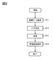
- FIG. 2 is a flowchart showing an example of the inspection method.
- 3A to 3C are schematic views showing an example of an inspection method.
- FIG. 4 is a flowchart showing an example of the inspection method.
- 5A to 5C are schematic views showing an example of an inspection method.
- 6A and 6B are schematic views showing an example of an inspection method.
- 7A and 7B are schematic views showing an example of an inspection method.
- FIG. 8 is a block diagram showing a configuration example of the inspection device.
- FIG. 9 is a block diagram showing a configuration example of the inspection device.
- 10A and 10B are diagrams showing a hierarchical neural network.
- FIG. 11 is a block diagram showing a configuration example of the arithmetic circuit.
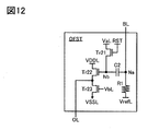
- FIG. 12 is a circuit diagram showing a configuration example of a circuit included in the arithmetic circuit.
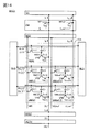
- FIG. 13 is a timing chart showing an operation example of the arithmetic circuit.
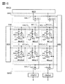
- FIG. 14 is a block diagram showing a configuration example of the arithmetic circuit.
- FIG. 15 is a block diagram showing a configuration example of the arithmetic circuit.
- FIG. 16 is a timing chart showing an operation example of the arithmetic circuit.
- FIG. 17A is a block diagram showing a configuration example of the storage device.
- FIG. 17B is a perspective view showing a configuration example of the storage device.
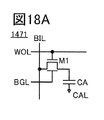
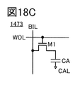
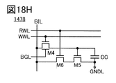
- 18A to 18H are circuit diagrams showing a configuration example of a storage device.
- FIG. 12 is a circuit diagram showing a configuration example of a circuit included in the arithmetic circuit.
- FIG. 13 is a timing chart showing an operation example of the arithmetic circuit.
- FIG. 14 is a block diagram showing a configuration example of the
- FIG. 19 is a schematic cross-sectional view showing a configuration example of the semiconductor device.
- FIG. 20 is a schematic cross-sectional view showing a configuration example of a semiconductor device.
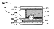
- 21A to 21C are schematic cross-sectional views showing a configuration example of a semiconductor device.
- 22A and 22B are schematic cross-sectional views showing a configuration example of a transistor.
- FIG. 23 is a schematic cross-sectional view showing a configuration example of the semiconductor device.
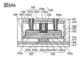
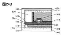
- 24A and 24B are schematic cross-sectional views showing a configuration example of a transistor.
- FIG. 25 is a schematic cross-sectional view showing a configuration example of the semiconductor device.
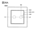
- FIG. 26A is a top view showing a configuration example of the capacitance.
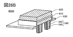
- FIG. 26B and 26C are cross-sectional perspective views showing a configuration example of the capacitance.
- FIG. 27A is a top view showing a configuration example of the capacitance.
- FIG. 27B is a cross-sectional view showing a configuration example of the capacitance.
- FIG. 27C is a cross-sectional perspective view showing a configuration example of the capacitance.
- FIG. 28A is a diagram showing the classification of the crystal structure of IGZO.
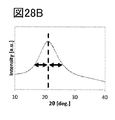
- FIG. 28B is a diagram showing an XRD spectrum of quartz glass.
- FIG. 28C is a diagram showing an XRD spectrum of crystalline IGZO.
- FIG. 28D is a diagram showing a microelectron diffraction pattern of crystalline IGZO.
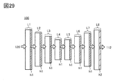
- FIG. 29 shows the configuration of the generator used in the embodiment.
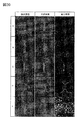
- FIG. 30 is an image according to an embodiment.
- 31A and 31B are images according to an embodiment.
- FIG. 32 is an image according to an embodiment.
- DOSRAM registered trademark
- 1T transistor
- 1C capacity
- NOSRAM Nonvolatile Oxide Semiconductor RAM
- DOSRAM Nonvolatile Oxide Semiconductor RAM
- One aspect of the present invention is an inspection device having an electron microscope, a PC (Personal Computer), and a server, and an inspection method using the inspection device.
- the shape of a fine sample such as a semiconductor device can be inspected. Specifically, for example, it is possible to inspect whether or not the sample has an abnormal portion.
- a PC and a server are collectively referred to as a computer.
- the electron microscope has a function of photographing a sample.
- the image taken by the electron microscope is sent to the computer as an inspection image.
- the computer has an AI chip which is a circuit in which a neural network is constructed, and the neural network is trained in advance using, for example, only an image of a sample having no abnormal portion as teacher data.
- the inspection image sent to the computer is input to the circuit in which the neural network is configured.
- the circuit produces an image. Therefore, it can be said that the circuit has a function as a generator.
- the training of the neural network is performed using, for example, only the image of the sample having no abnormal portion as the teacher data. Therefore, even if the inspection image input to the circuit in which the neural network is configured is an image including an abnormal portion, the abnormal portion disappears from the output image.
- the computer included in the inspection device of one aspect of the present invention performs smoothing processing on the inspection image and the image output from the neural network. Then, by taking the difference between the smoothed inspection image and the image output from the neural network, an abnormal portion included in the inspection image is detected.
- the inspection device of one aspect of the present invention can automatically detect an abnormality included in an inspection image with high accuracy.
- FIG. 1 is a block diagram showing a configuration example of the inspection device 1 which is one embodiment of the present invention.
- the inspection device 1 includes an electron microscope 10, an image processing device 80, a PC 20, and a server 30.
- the PC 20 and the server 30 are collectively referred to as a computer 40.
- the inspection device 1 having the configuration shown in FIG. 1 is suitable for inspecting the shape of a fine sample such as a semiconductor device. In particular, it is suitable for inspecting the shape of a sample of several ⁇ m or less.
- the electron microscope 10 will be described assuming SEM, but the present invention is not limited to this, and one embodiment of the present invention is a transmission electron microscope (TEM: Transmission Electron Microscope) or a scanning transmission electron microscope (TEM). It is also applicable to STEM: Scanning Transmission Electron Microscope).
- TEM Transmission Electron Microscope
- TEM scanning transmission electron microscope
- the electron microscope 10 includes an electron gun 11, a focusing lens 12, an objective lens 13, a scanning coil 14, a detector 15, and a stage 16. Further, although not shown, the electron microscope 10 has a vacuum pump and can keep the sample chamber in a vacuum state.
- the electron beam 17 emitted from the electron gun 11 is focused by the focusing lens 12 and the objective lens 13 and irradiated to the sample 18.
- the sample 18 emits a signal electron 19, and the signal electron 19 is detected by the detector 15.
- the signal electrons 19 include secondary electrons and backscattered electrons.
- the secondary electrons and backscattered electrons may be detected by separate detectors.
- the inspection device 1 can observe the surface shape and the like of the sample 18 by analyzing the intensity of the signal electron 19.
- the electron microscope 10 has a function of generating a signal corresponding to the surface shape and the like of the sample 18.
- the image processing device 80 has a function of converting a signal into an image.
- the image processing device 80 converts the signal detected by the detector 15 into an image.
- the image generated by the image processing device 80 is sent to the PC 20.
- the PC 20 has an input / output device 21.
- the user of the inspection device 1 can confirm the image generated by the image processing device 80 through the input / output device 21.
- the image is represented by a pixel value.
- the pixel value is, for example, a value representing the brightness of the light emitted by the pixel.
- the image can be represented by the same number of pixel values as the resolution.
- an image having a resolution of 1920 ⁇ 1080 can be represented by a pixel value of 1920 ⁇ 1080.
- the input / output device 21 is a so-called interface, and includes a display, a keyboard, a mouse, and the like.
- a touch sensor may be provided on the display.
- the PC 20 has a function of controlling the electron microscope 10, and can control the accelerating voltage of the electron beam, the position of the stage, and the like.
- the PC 20 is connected to the server 30 via a network, and can send the image taken by the electron microscope 10 to the server 30.
- the server 30 has a CPU (Central Processing Unit) 31, an AI chip 32, a main storage device 33, an auxiliary storage device 34, and a bus 35.
- CPU Central Processing Unit
- the server 30 can analyze the image signal sent from the PC 20 and send the analysis result to the PC 20.
- DRAM can be used as the main storage device 33. Further, DOSRAM or NOSRAM may be used as the main storage device 33. By using DOSRAM or NOSRAM, the power consumption of the server 30 can be suppressed.
- auxiliary storage device 34 an HDD (Hard Disk Drive) or an SSD (Solid State Drive) can be used. Further, NO SRAM may be used as the auxiliary storage device 34. By using NO SRAM, the power consumption of the server 30 can be suppressed.
- HDD Hard Disk Drive
- SSD Solid State Drive
- the AI chip 32 is a circuit in which a neural network is configured. It is preferable to use an OS transistor for the AI chip 32. By using an OS transistor in the AI chip 32, an analog neural network becomes possible, and the power consumption of the server 30 can be suppressed.
- the PC 20 may have the role of the server 30. In that case, the PC 20 preferably has an AI chip 32.
- the image taken by the electron microscope 10 is analyzed by the server 30.
- the server 30 can automatically detect an abnormal portion included in the image and notify the user of the inspection device 1 via the PC 20 and the input / output device 21.
- the sample 18 is assumed to be a semiconductor device, but the sample 18 is not limited to this.
- the sample 18 the whole sample whose shape is generally confirmed by an electron microscope is applicable.
- FIG. 2 shows a flowchart showing an example of the flow of the learning process
- FIGS. 3A to 3C are schematic views for explaining a part of the process of FIG. In this embodiment, a case of inspecting the wiring shape of the semiconductor device will be illustrated and described.
- the processing shown in FIG. 2 is preferably performed on the server 30, but in some cases, some or all of the processing may be performed on the PC 20.
- the teacher data 101 is acquired. It is preferable that the teacher data 101 is composed of only a plurality of non-defective images that do not include abnormal parts.
- the number of non-defective images is preferably 1,000 or more, more preferably 5,000 or more, and even more preferably 10,000 or more. If the number of non-defective images is large, more accurate learning is possible, but in reality, it is limited by the performance of the server 30 that performs learning. Specifically, it is limited by the processing capacity of the CPU 31 and the AI chip 32 and the storage capacity of the main storage device 33.
- step S11 it is preferable to convert the resolution of the image constituting the teacher data 101 into an appropriate value.
- the higher the resolution of the image the more accurate learning is possible, but in reality, it is limited by the performance of the server 30 that performs learning. Specifically, it is limited by the processing capacity of the CPU 31 and the AI chip 32 and the storage capacity of the main storage device 33.
- step S11 it is preferable that the number of channels of the image constituting the teacher data 101 is converted to 1, that is, grayscale.
- step S12 noise is added to all the images of the teacher data 101 to generate the data 102 (FIG. 3A).
- Examples of the noise to be added include Gaussian noise and the like.
- step S13 learning is performed. Learning is performed using the teacher data 101, the data 102, and the generator 100 (FIG. 3B).
- the generator 100 is a program using a neural network, and can generate an image for the input data.
- Examples of the generator 100 include an Autoencoder (AE), a Convolutional Autoencoder (CAE), and the like.
- AE Autoencoder
- CAE Convolutional Autoencoder
- GAN Generative Adversarial Networks
- DCGAN Deep Convolutional Generative Adversarial Networks
- the AI chip 32 has a function as a generator 100.
- the generator 100 uses the data 102 as input data and performs learning so that the output data approaches the teacher data 101 (updates the weight of the neural network).
- step S14 the learning result 103 is saved (FIG. 3B). More specifically, the weight of the generator 100 acquired by learning is stored.
- the above-mentioned learning is performed for each wiring shape to be inspected. That is, the learning result corresponding to the type of the wiring shape to be inspected is acquired.
- FIG. 3C shows three types of wiring shapes, which are teacher data 101a, teacher data 101b, and teacher data 101c, respectively. Further, as a result of using each teacher data for learning, a learning result 103a, a learning result 103b, and a learning result 103c are acquired. These learning results are stored in the auxiliary storage device 34 of the server 30.
- FIG. 4 is a flowchart showing an example of the flow of the inspection process described above, and FIGS. 5A to 5C, 6A, 6B, and 7A and 7B are schematics for explaining a part of the process of FIG. It is a figure.
- the processing shown in FIG. 4 is preferably performed on the server 30, but in some cases, some or all of the processing may be performed on the PC 20.
- the process of FIG. 4 is preferably performed by the PC 20.
- the PC 20 preferably has an AI chip 32.
- step S21 the server 30 acquires an image taken by the electron microscope 10.
- step S22 the server 30 checks whether the trained model corresponding to the acquired image exists in the auxiliary storage device 34. If it exists, the process proceeds to step S23, and if it does not exist, the inspection is terminated. Before the inspection is completed, it is preferable to output a message to the effect that the learned data does not exist to the input / output device 21 and notify the user of the inspection device 1.
- step S21 it is preferable that the resolution and the number of channels of the inspection image 110 are matched with the teacher data 101 in step S13 of FIG.
- step S23 noise is added to the inspection image 110 to generate an image 120 (FIG. 5A). It is desirable that the noise to be added is the same as that added in step S12 of FIG.
- step S24 the image 120 is input to the trained generator 100, and the image 112 is acquired (FIG. 5A).
- the generator 100 is in a state of reading the learning result 103 acquired by the prior learning, and the weight is updated.
- the generator 100 Since the generator 100 has learned only with the teacher data 101, which is a set of non-defective images, no information about the abnormal portion 111 is given. Therefore, the generator 100 cannot reproduce the abnormal portion 111, and the abnormal portion 111 disappears from the image 112.
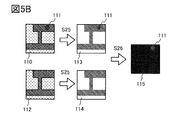
- step S25 the inspection image 110 is smoothed and the image 113 is acquired. Similarly, the image 112 is smoothed to obtain the image 114 (FIG. 5B). It is preferable that the smoothing process performed on the inspection image 110 and the image 112 is the same.
- a method of the smoothing process there is a method of calculating the convolution between the image and a filter called a kernel.
- a filter there are two types, an average filter and a Gaussian filter.
- the smoothing processing method a case where a 3 ⁇ 3 size average filter is used will be described.
- a 3 ⁇ 3 window centered on that pixel is selected for each pixel, and the total pixel values of all the pixels in the window is 9 Divide by. That is, it takes the average of the pixel values in the window.
- the size of the filter is not limited to Equation 1, and a size represented by an odd square such as 5 ⁇ 5 or 7 ⁇ 7 may be provided as needed.
- the weights of the average filters were all 1, but the Gaussian filter was given the weights of the filters according to the Gaussian distribution centered on the pixel of interest.
- the Gaussian filter When applying a Gaussian filter, specify the variance (or standard deviation) of the Gaussian distribution.
- the inspection image 110 often contains noise derived from the electron microscope 10. By performing the above-mentioned smoothing process, noise can be removed from the inspection image 110.
- step S26 the difference between the image 113 and the image 114 is taken.
- the image 115 is acquired by taking the difference between the pixel value representing the image 113 and the pixel value representing the image 114 (FIG. 5B).
- the difference is taken for each pixel value. That is, when the image 113 and the image 114 are represented by, for example, 1920 ⁇ 1080 pixel values, a difference is taken for each of the 1920 ⁇ 1080 pixel values. Therefore, when the image 113 and the image 114 are each represented by 1920 ⁇ 1080 pixel values, the image 115 can also be represented by 1920 ⁇ 1080 pixel values.
- the difference between the image 113 and the image 114 is close to zero. Therefore, in the image 115, the brightness is close to 0 except for the abnormal portion 111.
- step S27 the brightness of the pixels of the image 115 is converted into a binary value of 1 or 0 based on a certain threshold value. By doing so, it is possible to acquire an image 116 in which the abnormal portion 111 is painted white and the portion other than the abnormal portion 111 is painted black (FIG. 5C).
- the image 116 is an image in which the abnormal portion 111 is emphasized.
- step S28 outlier detection of the image 116 is performed, and the image 116 is classified into either abnormal data or normal data. That is, the machine determines the quality of the inspection image 110.
- an appropriate method such as a k-nearest neighbor method, a k-means method, a LOF (Local Outlier Factor), or an SVM (Support Vector Machine) method may be used.
- the degree of abnormality of the image 116 by a certain numerical value.
- the number of pixels whose brightness is represented by 1 the number of pixels filled in white
- the distance from the center of gravity of the set clustered as normal data may be used as the degree of anomaly.
- the distance from the boundary between normal and abnormal determined by the machine may be used as the degree of abnormality.
- weighting may be performed for abnormalities.
- the magnitude of the weight can be different for each type of anomaly, for example. For example, anomalies that have a large effect on the quality of the test sample can be given a large weight.
- weighting an abnormality for example, all the abnormality points 111 detected from the inspection image 110 can be weighted, and the total weight can be used as the degree of abnormality.
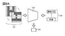
- FIG. 6A and 6B are schematic views for explaining an example of a weighting method for anomalies.
- FIG. 6A is a schematic diagram for explaining an example of the learning method, and is performed in advance.
- FIG. 6B is a schematic diagram for explaining an example of a method of determining the type of abnormality from an inspection image including an abnormality by using the learning result.
- FIGS. 6A and 6B are preferably performed on the server 30, but in some cases, some or all of the processes may be performed on the PC 20.
- the process of FIG. 6B is preferably performed by the PC 20.
- the PC 20 preferably has an AI chip 32.
- the image data 131 is acquired, and the label 132 is associated with each of the acquired image data 131.
- the image data 131 is preferably composed of only a plurality of defective image images including abnormal parts.
- the label 132 may represent, for example, the type of abnormality shown in the image data 131.
- the type of abnormality can be, for example, disconnection, short circuit, foreign matter adhesion, cavity formation, or the like.
- the number of defective image images is, for example, preferably 1,000 or more, more preferably 5,000 or more, and more preferably 10,000 or more for one type of abnormality. If the number of defective images is large, more accurate learning is possible, but in reality, it is limited by the performance of the server 30 that performs learning. Specifically, it is limited by the processing capacity of the CPU 31 and the AI chip 32 and the storage capacity of the main storage device 33.
- the resolution of the image constituting the image data 131 it is preferable to convert the resolution of the image constituting the image data 131 to an appropriate value.
- the higher the resolution of the image the more accurate learning is possible, but in reality, it is limited by the performance of the server 30 that performs learning. Specifically, it is limited by the processing capacity of the CPU 31 and the AI chip 32 and the storage capacity of the main storage device 33.
- the number of channels of the image constituting the image data 131 is 1, that is, converted to gray scale.
- the learning is performed using the image data 131, the label 132, and the classifier 130 (FIG. 6A).
- the classifier 130 is a program using a neural network, and can extract the feature amount of the input image and generate a feature map.
- Examples of the classifier 130 include a convolutional neural network (CNN: Convolutional Neural Network) and the like. It can be said that the AI chip 32 has a function as a classifier 130.
- the classifier 130 uses the image data 131 and the label 132 as teacher data, and performs learning so that the output data becomes desired (updates the weight of the neural network). For example, when the classifier 130 outputs a feature map, learning is performed so that the classifier 130 can appropriately extract the feature amount of the image data 131 input to the classifier 130 according to the label 132.
- the learning result 133 is saved (FIG. 6A). More specifically, the weight of the classifier 130 acquired by learning is stored. This is the end of learning.
- step S28 shown in FIG. 4 the inspection image in which the abnormality is detected is input to the trained classifier 130.
- FIG. 6B shows an example in which the inspection image 110 including the abnormal portion 111 is input to the classifier 130.
- the classifier 130 is in a state of reading the learning result 133 acquired by the prior learning, and the weight is updated.
- data 134 indicating the type of abnormality included in the inspection image is output from the classifier 130 based on the learning result 133.
- the degree of abnormality of the inspection image 110 including the abnormal portion 111 is calculated.
- the degree of anomaly can be a value obtained by multiplying the number of anomalies by the weight corresponding to the data 134.
- the inspection image 110 is smoothed to obtain an image 113, and the image 112 is smoothed to obtain an image 114, and then the image 113 is used. Take the difference of the image 114.
- the inspection image 110 often contains noise derived from the electron microscope 10. Therefore, if the difference is taken without performing the smoothing process, the abnormal portion 111 may not be detected correctly. Therefore, by taking the difference after performing the smoothing process, the inspection device 1 can automatically detect the abnormal portion 111 included in the inspection image 110 with high accuracy.
- FIG. 7A is a schematic diagram showing an example in which the above-mentioned inspection result is displayed on the input / output device 21.
- FIG. 7A shows a terminal provided with a touch panel and a display as an example of the input / output device 21.
- the inspection images are displayed side by side in the order of the degree of abnormality acquired in step S28.
- FIG. 7A shows an example in which the image on the left side has a smaller degree of abnormality and the image on the right side has a larger degree of abnormality (Abnormal). That is, good products are on the left side, and defective products are on the right side.
- the result (Good / Bad) of the quality determination by the machine in step S28 is displayed on each image.
- FIG. 7A shows an example in which the inspection image 110 touched by the user of the inspection device 1 and the image 117 are displayed.
- Image 117 is a composite of the inspection image 110 and the image 116 of FIG. 5C. That is, it is an image in which the abnormal portion of the inspection image 110 is emphasized.
- the user of the inspection device 1 can easily determine the abnormal portion included in the inspection image.
- the color of the abnormal portion may be displayed in gradation according to the brightness of the image 115 in FIG. 5B.
- the input / output device 21 allows the user to correct the Good / Bad result determined by the machine.
- the correction result can be transmitted to the server 30 and reflected in the future pass / fail judgment.
- the images existing near the left and right ends are unlikely to be judged differently between the machine and the user of the inspection device 1.
- the image existing near the center of the screen is often judged differently between the machine and the user of the inspection device 1.
- FIG. 7B is a schematic view showing a display example of the input / output device 21 when weighting an abnormal portion of the inspection image 110.
- the weight can be made larger as the influence on the quality of the test sample is greater, for example. Weighting can be performed by the method shown in FIGS. 6A and 6B.
- FIG. 7B shows an example in which the image 117 corresponding to the inspection image 110 touched by the user of the inspection device 1 is displayed.
- the image 117 shown in FIG. 7B includes two abnormal locations.
- one of the abnormal parts does not cause disconnection, short circuit, etc., and the influence of the abnormality on the quality of the inspection sample is small.
- the other abnormal portion causes, for example, a disconnection, and the abnormality has a great influence on the quality of the inspection sample. Therefore, the weight of the other abnormal portion is made larger than the weight of one abnormal portion.
- FIG. 7B shows a display example of the input / output device 21 when the weight of one abnormal portion is 2 and the weight of the other abnormal portion is 10. As shown in FIG. 7B, the weight can be displayed for each abnormal portion.
- FIG. 7B shows a display example of the input / output device 21 when the total weight is 5 or less, it is determined to be a good product (Good), and when it is 6 or more, it is determined to be a defective product (Bad).
- the determination criteria for good products (Good) and defective products (Bad) can be displayed on the input / output device 21.
- the abnormal part By weighting the abnormal part, it is possible to judge the quality of the test sample with high accuracy. Further, by displaying the weight on the input / output device 21, the user of the inspection device 1 can easily recognize the cause of the defect of the sample.
- the inspection device of the present embodiment it is possible to automatically detect an abnormality included in the inspection image with high accuracy. In addition, it can be automatically detected with low power consumption.
- the inspection method of the present embodiment it is possible to automatically detect an abnormality included in the inspection image with high accuracy. In addition, it can be automatically detected with low power consumption.
- an image taken by an electron microscope is assumed as an inspection image in which the inspection apparatus of one aspect of the present invention determines an abnormality, but one aspect of the present invention is not limited to this.
- a configuration example of the inspection device according to one aspect of the present invention will be described when an image other than the image taken by the electron microscope is used as the inspection image.
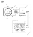
- FIG. 8 is a block diagram showing a configuration example of the inspection device 1a.
- the inspection device 1a differs from the inspection device 1 shown in the first embodiment in that it has a computed tomography apparatus 50 instead of the electron microscope 10.
- the computed tomography apparatus 50 has a gantry 51 and a cradle 52.
- the gantry 51 is provided with an opening 61, and an X-ray tube 71 and a detector 72 are provided so as to have a region in contact with the side wall of the opening 61.
- the subject 62 is placed in the cradle 52.
- the subject 62 can be, for example, the human body.
- the X-ray tube 71 has a function of emitting, for example, X-rays (for example, an electromagnetic wave having a wavelength of 1 pm or more and 10 nm or less).
- the detector 72 has a function of detecting, for example, X-rays.
- the electromagnetic wave emitted from the X-ray tube 71 is irradiated to the subject 62, a part of the irradiated electromagnetic wave is absorbed by the subject 62.
- the electromagnetic wave transmitted without being absorbed by the subject 62 is irradiated to the detector 72.
- the signal representing the intensity of the electromagnetic wave applied to the detector 72 is converted into an image by the image processing device 80.
- the inspection device 1 shown in the first embodiment can be referred to.
- the PC 20 included in the inspection device 1a has a function of controlling the computed tomography device 50, and can control the position of the X-ray tube 71, for example.
- the electron microscope 10 is read as the computed tomography device 50, the sample is read as the subject, and the like, the description of the inspection method using the inspection device 1 shown in the first embodiment will be described. You can refer to it.
- FIG. 9 is a block diagram showing a configuration example of the inspection device 1b.
- the inspection device 1b is different from the inspection device 1 shown in the first embodiment in that it has a nuclear magnetic resonance device 210 instead of the electron microscope 10.
- the nuclear magnetic resonance apparatus 210 has a gantry 211 and a cradle 212.
- the gantry 211 is provided with an opening 221.
- a coil 231 is provided inside the gantry 211 so as to cover the side wall of the opening 221.
- Subject 222 is placed in the cradle 212.
- the subject 222 can be, for example, a human body in the same manner as the subject 62 shown in FIG.
- the subject 222 is preferably a living body.
- the coil 231 has a function of generating a magnetic field.
- a resonance phenomenon occurs between the hydrogen atom contained in the subject 222 and the magnetic field.
- a nuclear magnetic resonance signal is generated.
- the nuclear magnetic resonance signal is converted into an image by the image processing device 80.
- the inspection device 1 shown in the first embodiment can be referred to.
- the PC 20 included in the inspection device 1b has a function of controlling the nuclear magnetic resonance device 210, and can switch the direction of the magnetic field generated by the coil 231, for example.
- the electron microscope 10 is read as a nuclear magnetic resonance device 210, the sample is read as a subject, and the like, the description of the inspection method using the inspection device 1 shown in the first embodiment will be described. Can be referred to.
- a hierarchical neural network has one input layer, one or more intermediate layers (hidden layers), and one output layer, and is composed of a total of three or more layers.
- the hierarchical neural network 200 shown in FIG. 10A shows an example thereof, and the neural network 200 has a first layer to an R layer (R here can be an integer of 4 or more). ing.
- R can be an integer of 4 or more
- the first layer corresponds to the input layer
- the R layer corresponds to the output layer
- the other layers correspond to the intermediate layer.
- FIG. 10A shows the (k-1) th layer and the kth layer (k here is an integer of 3 or more and R-1 or less) as intermediate layers, and other intermediate layers. Is not shown.
- Each layer of the neural network 200 has one or more neurons.
- layer 1 has neurons N 1 (1) to neuron N p (1) (where p is an integer greater than or equal to 1), and layer (k-1) is neuron N 1. (K-1) to neuron N m (k-1) (where m is an integer of 1 or more), and the k-th layer has neurons N 1 (k) to neurons N n (k) ( Here, n is an integer of 1 or more), and the R layer has neurons N 1 (R) to neurons N q (R) (q here is an integer of 1 or more). ..
- the values of m and n may be greater than or equal to p and less than or equal to p. Further, the values of m and n may be q or more and less than q. For example, when the neural network 200 has a function as an autoencoder (AE), the values of m and n can be less than p and q.
- AE autoencoder
- 10B is a neuron N j of the k-th layer (k), shows the signal which is input to the neuron N j (k), a signal output from the neuron N j (k), the.
- z 1 (k-1) to z m (k- ), which are output signals of neurons N 1 (k-1) to N m (k-1) in the (k-1) layer , respectively. 1) is output toward the neuron Nj (k) .
- the neuron N j (k) is, z 1 (k-1) to z m (k-1) to generate a z j (k) in response to, the z j (k) is an output signal (k + 1 ) Output to each neuron in the layer (not shown).
- the degree of signal transmission of signals input from neurons in the previous layer to neurons in the next layer is determined by the strength of synaptic connections (hereinafter referred to as weighting factors) that connect these neurons.
- weighting factors the strength of synaptic connections that connect these neurons.
- the signal output from the neurons in the previous layer is multiplied by the corresponding weighting factor and input to the neurons in the next layer.
- i an integer 1 or m
- the signal input to the neuron N j (k) in the k-th layer can be expressed by the equation (D1).
- the result of the sum of products may be biased as a bias.
- the equation (D2) can be rewritten as the following equation.
- the neuron N j (k) produces an output signal z j (k) in response to u j (k) .
- Neuron N j output signal z j from (k) (k) defined by the following equation.
- the function f (u j (k) ) is an activation function in a hierarchical neural network, and a step function, a linear ramp function, a sigmoid function, or the like can be used.
- the activation function may be the same or different in all neurons.
- the activation function of neurons may be the same or different in each layer.
- the signal, the weighting coefficient w, or the bias b output by the neurons in each layer may be an analog value or a digital value.
- the digital value may be, for example, a binary value or a ternary value. A value with a larger number of bits may be used.
- an analog value for example, a linear ramp function, a sigmoid function, or the like may be used as the activation function.
- binary digital values for example, a step function with an output of -1 or 1 or 0 or 1 may be used.
- the signal output by the neurons in each layer may have three or more values.
- the activation function has three or more values, for example, a step function whose output is -1, 0, or 1, or 0, 1, or.
- a step function or the like set to 2 may be used.
- a step function of -2, -1, 0, 1, or 2 may be used.
- the neural network 200 is sequentially input from the front layer in each layer from the first layer (input layer) to the last layer (output layer). Based on the signal, an output signal is generated using the equation (D1), the equation (D2) (or the equation (D3)), and the equation (D4), and the output signal is output to the next layer.
- the signal output from the last layer (output layer) corresponds to the result calculated by the neural network 200.
- FIG. 11 shows a configuration example of the arithmetic circuit MAC1.
- the arithmetic circuit MAC1 shown in FIG. 11 performs a product-sum operation of the first data held in the memory cell described later and the input second data, and activates the activation function using the result of the product-sum operation. It is a circuit that performs the calculation of.
- the first data and the second data can be analog data or multi-valued data (discrete data) as an example.
- the arithmetic circuit MAC1 includes a current source circuit CS, a current mirror circuit CM, a circuit WDD, a circuit WLD, a circuit CLD, a circuit OFST, an activation function circuit ACTV, and a memory cell array CA.
- the memory cell array CA has a memory cell AM [1], a memory cell AM [2], a memory cell AMref [1], and a memory cell AMref [2].
- the memory cell AM [1] and the memory cell AM [2] have a role of holding the first data, and the memory cell AMref [1] and the memory cell AMref [2] are used to perform the product-sum operation. It has a function to hold the required reference data.
- the reference data can be analog data or multi-valued data (discrete data) as well as the first data and the second data.
- the memory cell array CA of FIG. 11 two memory cells are arranged in the row direction and two in the column direction in a matrix, whereas in the memory cell array CA, three or more memory cells are arranged in the row direction and columns. Three or more in the direction may be arranged in a matrix. Further, when multiplication is performed instead of the multiply-accumulate operation, the memory cell array CA may be configured such that one memory cell in the row direction and two or more memory cells in the column direction are arranged in a matrix.
- the memory cell AM [1], the memory cell AM [2], the memory cell AMref [1], and the memory cell AMref [2] have a transistor Tr11, a transistor Tr12, and a capacitance C1, respectively.
- the transistor Tr11 is preferably an OS transistor.
- the channel formation region of the transistor Tr11 is indium, element M (element M is, for example, aluminum, gallium, yttrium, copper, vanadium, beryllium, boron, titanium, iron, nickel, germanium, zirconium, molybdenum, lantern. , One or more selected from cerium, neodymium, hafnium, tantalum, tungsten, gallium and the like.), It is more preferable that the oxide contains at least one of zinc. It is more preferable that the transistor Tr11 has a transistor structure described in the following embodiments.
- the leakage current of the transistor Tr11 can be suppressed, so that a product-sum calculation circuit with high calculation accuracy may be realized. Further, by using the OS transistor as the transistor Tr11, the leakage current from the holding node to the writing word line when the transistor Tr11 is in the non-conducting state can be made very small. That is, since the potential refresh operation of the holding node can be reduced, the power consumption of the product-sum calculation circuit can be reduced.
- the transistor Tr12 can be manufactured at the same time as the transistor Tr11, so that the manufacturing process of the product-sum calculation circuit may be shortened.
- the channel forming region of the transistor Tr12 may contain silicon instead of oxide.
- the silicon for example, amorphous silicon, microcrystalline silicon, polycrystalline silicon, single crystal silicon, hydride amorphous silicon and the like may be used.
- the first terminal of the transistor Tr11 is the gate of the transistor Tr12 and electricity. Is connected.
- the first terminal of the transistor Tr12 is electrically connected to the wiring VR.
- the first terminal of the capacitance C1 is electrically connected to the gate of the transistor Tr12.
- the second terminal of the transistor Tr11 is electrically connected to the wiring WD, and the gate of the transistor Tr11 is electrically connected to the wiring WL [1].
- the second terminal of the transistor Tr12 is electrically connected to the wiring BL, and the second terminal of the capacitance C1 is electrically connected to the wiring CL [1].
- the connection point between the first terminal of the transistor Tr11, the gate of the transistor Tr12, and the first terminal of the capacitance C1 is a node NM [1].
- the current flowing from the wiring BL to the second terminal of the transistor Tr12 is defined as I AM [1] .
- the second terminal of the transistor Tr11 is electrically connected to the wiring WD, and the gate of the transistor Tr11 is electrically connected to the wiring WL [2].
- the second terminal of the transistor Tr12 is electrically connected to the wiring BL, and the second terminal of the capacitance C1 is electrically connected to the wiring CL [2].
- the connection point between the first terminal of the transistor Tr11, the gate of the transistor Tr12, and the first terminal of the capacitance C1 is a node NM [2].
- the current flowing from the wiring BL to the second terminal of the transistor Tr12 is defined as I AM [2] .
- the second terminal of the transistor Tr11 is electrically connected to the wiring WDref, and the gate of the transistor Tr11 is electrically connected to the wiring WL [1].
- the second terminal of the transistor Tr12 is electrically connected to the wiring BLref, and the second terminal of the capacitance C1 is electrically connected to the wiring CL [1].
- the connection point between the first terminal of the transistor Tr11, the gate of the transistor Tr12, and the first terminal of the capacitance C1 is a node NMref [1].
- the current flowing from the wiring BLref to the second terminal of the transistor Tr12 is defined as IAMref [1] .
- the second terminal of the transistor Tr11 is electrically connected to the wiring WDref, and the gate of the transistor Tr11 is electrically connected to the wiring WL [2].
- the second terminal of the transistor Tr12 is electrically connected to the wiring BLref, and the second terminal of the capacitance C1 is electrically connected to the wiring CL [2].
- the connection point between the first terminal of the transistor Tr11, the gate of the transistor Tr12, and the first terminal of the capacitance C1 is a node NMref [2].
- the current flowing from the wiring BLref to the second terminal of the transistor Tr12 is defined as IAMref [2] .
- node NM [1], node NM [2], node NMref [1], and node NMref [2] function as holding nodes of their respective memory cells.
- the wiring VR allows a current to flow between the first terminal and the second terminal of each transistor Tr12 of the memory cell AM [1], the memory cell AM [2], the memory cell AMref [1], and the memory cell AMref [2].
- Wiring for. Therefore, the wiring VR functions as a wiring for giving a predetermined potential.
- the potential given by the wiring VR can be a reference potential or a potential lower than the reference potential.
- the current source circuit CS is electrically connected to the wiring BL and the wiring BLref.
- the current source circuit CS has a function of supplying a current to the wiring BL and the wiring BLref.
- the amount of current supplied to each of the wiring BL and the wiring BLref may be different from each other. In this configuration example, the current flowing from the current source circuit CS wiring BL and I C, the current flowing from the current source circuit CS wiring BLref and I Cref.
- the current mirror circuit CM has a wiring IL and a wiring ILref.
- the wiring IL is electrically connected to the wiring BL, and in FIG. 11, the connection point between the wiring IL and the wiring BL is shown as a node NP.
- the wiring ILref is electrically connected to the wiring BLref, and in FIG. 11, the connection point between the wiring ILref and the wiring BLref is a node NPref.
- the current mirror circuit CM has a function of discharging a current corresponding to the potential of the node NPref from the node NPref of the wiring BLref to the wiring ILref, and discharging the same amount of current from the node NP of the wiring BL to the wiring IL.
- the circuit WDD is electrically connected to the wiring WD and the wiring WDref.
- the circuit WDD has a function of transmitting data to be stored in each memory cell of the memory cell array CA.
- the circuit WLD is electrically connected to the wiring WL [1] and the wiring WL [2].
- the circuit WLD has a function of selecting a memory cell to write data to when writing data to a memory cell included in the memory cell array CA.
- the circuit CLD is electrically connected to the wiring CL [1] and the wiring CL [2].
- the circuit CLD has a function of applying a potential to the second terminal of the capacity C1 of each memory cell of the memory cell array CA.
- the circuit OFST is electrically connected to the wiring BL and the wiring OL.
- the circuit OFST has a function of measuring the amount of current flowing from the wiring BL to the circuit OFST and / or the amount of change in the current flowing from the wiring BL to the circuit OFST.
- the circuit OFST has a function of outputting the measurement result to the wiring OL.
- the circuit OFST may be configured to output the measurement result as a current to the wiring OL as it is, or may be configured to convert the measurement result into a voltage and output it to the wiring OL.
- the current flowing from the wiring BL to the circuit OFST is indicated by I ⁇ .
- the circuit OFST can have the configuration shown in FIG. In FIG. 12, the circuit OFST includes a transistor Tr21, a transistor Tr22, a transistor Tr23, a capacitance C2, and a resistance element R1.
- the first terminal of the capacitance C2 is electrically connected to the wiring BL, and the first terminal of the resistance element R1 is electrically connected to the wiring BL.
- the second terminal of the capacitance C2 is electrically connected to the first terminal of the transistor Tr21, and the first terminal of the transistor Tr21 is electrically connected to the gate of the transistor Tr22.
- the first terminal of the transistor Tr22 is electrically connected to the first terminal of the transistor Tr23, and the first terminal of the transistor Tr23 is electrically connected to the wiring OL.
- the electrical connection point between the first terminal of the capacitance C2 and the first terminal of the resistance element R1 is a node Na, the second terminal of the capacitance C2, the first terminal of the transistor Tr21, and the gate of the transistor Tr22. Let the electrical connection point of, be node Nb.
- the second terminal of the resistance element R1 is electrically connected to the wiring VrefL.
- the second terminal of the transistor Tr21 is electrically connected to the wiring VaL, and the gate of the transistor Tr21 is electrically connected to the wiring RST.
- the second terminal of the transistor Tr22 is electrically connected to the wiring VDDL.
- the second terminal of the transistor Tr23 is electrically connected to the wiring VSSL, and the gate of the transistor Tr23 is electrically connected to the wiring VbL.
- the wiring VrefL is a wiring that gives the potential Vref
- the wiring VaL is a wiring that gives the potential Va
- the wiring VbL is a wiring that gives the potential Vb.
- the wiring VDDL is the wiring that gives the potential VDD
- the wiring VSSL is the wiring that gives the potential VSS.
- the potential VDD is set to a high level potential
- the potential VSS is set to a low level potential.
- the wiring RST is a wiring that gives a potential for switching between a conductive state and a non-conducting state of the transistor Tr21.
- the source follower circuit is composed of the transistor Tr22, the transistor Tr23, the wiring VDDL, the wiring VSSL, and the wiring VbL.
- the resistance element R1 and the wiring VrefL give the node Na a current flowing from the wiring BL and a potential corresponding to the resistance of the resistance element R1.
- the first current (hereinafter referred to as the first current) flows from the wiring BL, the potential corresponding to the first current and the resistance of the resistance element R1 to the node Na by the resistance element R1 and the wiring VrefL. Is given.
- the transistor Tr21 is brought into a conductive state, and the potential Va is given to the node Nb. After that, the transistor Tr21 is put into a non-conducting state.
- the second current (hereinafter referred to as the second current) flows from the wiring BL
- the resistance element R1 and the wiring VrefL make the node Na the same as when the first current flows.
- a potential corresponding to the second current and the resistance of the resistance element R1 is given.
- the potential of the node Nb since the node Nb is in a floating state, the potential of the node Nb also changes due to the capacitive coupling due to the change in the potential of the node Na.
- the change in the potential of the node Na is ⁇ V Na and the capacitive coupling coefficient is 1, the potential of the node Nb is Va + ⁇ V Na .
- the potential Va + ⁇ V Na ⁇ V th is output from the wiring OL.
- the potential ⁇ V Na can be output from the wiring OL.
- the potential ⁇ V Na is determined according to the amount of change from the first current to the second current, the resistance value of the resistance element R1, and the potential Vref. Since the resistance value of the resistance element R1 and the potential Vref can be known, the amount of change in the current flowing through the wiring BL can be obtained from the potential ⁇ V Na by using the circuit OFST shown in FIG. ..
- the activation function circuit ACTV is electrically connected to the wiring OL and the wiring NIL.
- the result of the amount of change in the current measured by the circuit OFST is input to the activation function circuit ACTV via the wiring OL.
- the activation function circuit ACTV is a circuit that performs an operation according to a predefined function system on the result.
- a function system for example, a sigmoid function, a tanh function, a softmax function, a ReLU function, a threshold function and the like can be used, and these functions are applied as activation functions in a neural network.
- FIG. 13 shows a timing chart of an operation example of the arithmetic circuit MAC1.
- the timing chart of FIG. 13 shows the wiring WL [1], the wiring WL [2], the wiring WD, the wiring WDref, the node NM [1], the node NM [2], the node NMref [1], at the time T01 to the time T09.
- the current I B -I alpha from the wiring BL, the memory cell AM of the memory cell array CA [1], indicate the sum of the current flowing through the memory cell AM [2].
- ⁇ From time T01 to time T02 a high level potential (denoted as High in FIG. 13) is applied to the wiring WL [1], and a low level potential (Low in FIG. 13) is applied to the wiring WL [2]. Indicated.) Is applied. In addition, a potential V PR ⁇ V W [1] larger than the ground potential (denoted as GND in FIG. 13) is applied to the wiring WD, and a potential V PR larger than the ground potential is applied to the wiring WDref. It has been applied. Further, a reference potential (denoted as REFP in FIG. 13) is applied to the wiring CL [1] and the wiring CL [2], respectively.
- REFP reference potential
- the potential V W [1] is a potential corresponding to one of the first data. Further, the potential V PR is a potential corresponding to the reference data.
- V th is the threshold voltage of the transistor Tr12.
- I AMref [1], 0 I AMref [1] 0 is as follows. It can be expressed by an expression.
- the time starts from time T02. Until T03, the respective potentials of the node NM [1], the node NM [2], the node NMref [1], and the node NMref [2] are maintained.
- the OS is applied to each transistor Tr11 of the memory cell AM [1], the memory cell AM [2], the memory cell AMref [1], and the memory cell AMref [2].
- the transistor By applying the transistor, the leakage current flowing between the first terminal and the second terminal of the transistor Tr11 can be reduced, so that the node NM [1], the node NM [2], the node NMref [1], and the node Each potential of NMref [2] can be held for a long time.
- a ground potential is applied to the wiring WD and the wiring WDref. Since the transistors Tr11 of the memory cell AM [1], the memory cell AM [2], the memory cell AMref [1], and the memory cell AMref [2] are in the off state, the wiring WD and the wiring WDref are used. By applying the potential of, the potentials held in each of the node NM [1], the node NM [2], the node NMref [1], and the node NMref [2] are not rewritten.
- the potential V W [2] is a potential corresponding to one of the first data.
- I AMref [2], 0 When the current flowing from the wiring BLref to the first terminal via the second terminal of the transistor Tr12 of the memory cell AMref [2] is set to I AMref [2], 0 , similarly, I AMref [2], 0 is as follows. It can be expressed by an expression.
- the current from the current source circuit CS is supplied to the wiring BLref.
- a current is discharged to the wiring BLref by the current mirror circuit CM, the memory cell AMref [1], and the memory cell AMref [2].
- the following equation holds according to Kirchhoff's law.
- the current from the current source circuit CS is supplied to the wiring BL.
- a current is discharged to the wiring BL by the current mirror circuit CM, the memory cell AM [1], and the memory cell AM [2].
- a current flows from the wiring BL to the circuit OFST.
- the current supplied from the current source circuit CS and I C the current flowing from the wiring BL to the circuit OFST I alpha, when a 0, the following expression holds with Kirchhoff's law.
- the potential V X [1] is a potential corresponding to one of the second data.
- the increase in the potential of the gate of the transistor Tr12 is the potential obtained by multiplying the potential change of the wiring CL [1] by the capacitive coupling coefficient determined by the configuration of the memory cell.
- the capacitive coupling coefficient is calculated from the capacitance of the capacitance C1, the gate capacitance of the transistor Tr12, the parasitic capacitance, and the like.
- the increase in the potential of the wiring CL [1] and the increase in the potential of the gate of the transistor Tr12 are described as the same value. This corresponds to setting each capacitance coupling coefficient in the memory cell AM [1] and the memory cell AMref [1] to 1.
- the capacitance coupling coefficient is 1, the potential V X [1] is applied to the second terminal of each capacitance C1 of the memory cell AM [1] and the memory cell AMref [1], so that the node NM [ 1] The potentials of 1] and the node NMref [1] increase by V X [1] , respectively.
- I AMref [1], 1 is as follows. It can be expressed by an expression.
- the wiring BLref like the period from time T04 to time T05, the current I Cref from the current source circuit CS are supplied. At the same time, a current is discharged to the wiring BLref by the current mirror circuit CM, the memory cell AMref [1], and the memory cell AMref [2].
- the current discharged by the current mirror circuit CM is ICM , 1 , the following equation holds according to Kirchhoff's law.
- the wiring BL similar to the period from time T04 to time T05, the current I C from the current source circuit CS are supplied. At the same time, a current is discharged to the wiring BL by the current mirror circuit CM, the memory cell AM [1], and the memory cell AM [2]. Further, a current flows from the wiring BL to the circuit OFST. In the wiring BL, when the current flowing from the wiring BL to the circuit OFST is I ⁇ , 1 , the following equation holds according to Kirchhoff's law.
- ⁇ I ⁇ Difference between the current I ⁇ , 0 flowing from the wiring BL to the circuit OFST between the time T04 and the time T05 and the current I ⁇ , 1 flowing from the wiring BL to the circuit OFST between the time T05 and the time T06.
- ⁇ I ⁇ will be referred to as a differential current in the arithmetic circuit MAC1.
- the differential current ⁇ I ⁇ can be expressed by the following equations using the equations (E1) to (E10).
- a reference potential is applied to the wiring CL [1] between the time T06 and the time T07.
- the reference potential is applied to the second terminal of the respective capacities C1 of the memory cell AM [1] and the memory cell AMref [1]
- the potentials of the node NM [1] and the node NMref [1] are applied. Returns to the potentials between time T04 and time T05, respectively.
- a potential V X [1] higher than the reference potential is applied to the wiring CL [1]
- a potential V X [2] higher than the reference potential is applied to the wiring CL [2].
- the potential V X [1] is applied to the second terminal of the respective capacities C1 of the memory cell AM [1] and the memory cell AMref [1], and the memory cell AM [2] and the memory cell AMref [2 ] are applied.
- the potential V X [2] is applied to the second terminal of each capacitance C1. Therefore, the potential of the gate of each transistor Tr12 of the memory cell AM [1], the memory cell AM [2], the memory cell AMref [1], and the memory cell AMref [2] rises.
- the capacitance coupling coefficient is 1, the potential V X [2] is applied to the second terminal of each capacitance C1 of the memory cell AM [2] and the memory cell AMref [2], so that the node NM [ 2] The potentials of 2] and the node NMref [2] rise by V X [2] , respectively.
- I AMref [2], 1 is as follows. It can be expressed by an expression.
- the wiring BLref like the period from time T04 to time T05, the current I Cref from the current source circuit CS are supplied. At the same time, a current is discharged to the wiring BLref by the current mirror circuit CM, the memory cell AMref [1], and the memory cell AMref [2].
- the current discharged by the current mirror circuit CM is ICM , 2 , the following equation holds according to Kirchhoff's law.
- the wiring BL similar to the period from time T04 to time T05, the current I C from the current source circuit CS are supplied. At the same time, a current is discharged to the wiring BL by the current mirror circuit CM, the memory cell AM [1], and the memory cell AM [2]. Further, a current flows from the wiring BL to the circuit OFST. In the wiring BL, when the current flowing from the wiring BL to the circuit OFST is I ⁇ , 3 , the following equation holds according to Kirchhoff's law.
- the differential current ⁇ I ⁇ to be obtained can be expressed by the following equations using the equations (E1) to (E8) and the equations (E12) to (E15).
- the difference current ⁇ I ⁇ input to the circuit OFST is a potential V W which is a plurality of first data and a potential V X which is a plurality of second data.
- the value corresponds to the sum of the products. That is, the value of the sum of products of the first data and the second data can be obtained by measuring the differential current ⁇ I ⁇ in the circuit OFST.
- a reference potential is applied to the wiring CL [1] and the wiring CL [2] between the time T08 and the time T09.
- the reference potential is applied to the second terminal of each capacitance C1 of the memory cell AM [1], the memory cell AM [2], the memory cell AMref [1], and the memory cell AMref [2].
- the potentials of the node NM [1], the node NM [2], the node NMref [1], and the node NMref [2] return to the potentials between the time T06 and the time T07, respectively.
- the potential applied to the wiring CL [1] and the wiring CL [2] may be lower than the reference potential REFP.
- REFP a potential lower than the reference potential REFP is applied to the wiring CL [1] and / or the wiring CL [2]
- the memory cell connected to the wiring CL [1] and / or the wiring CL [2] The potential of the holding node can be lowered by capacitive coupling.
- the product of the first data and one of the second data having a negative value can be performed.
- the wiring CL [2] the case of applying -V X [2] rather than V X [2]
- the differential current [Delta] I alpha expressed as the following formula be able to.
- a memory cell array CA having memory cells arranged in a matrix of 2 rows and 2 columns was dealt with, but a memory cell array with 1 row and 2 columns or more, or 3 rows or more and 3 columns.
- the product-sum operation can be performed on the above memory cell array.
- the product-sum calculation circuit uses one of the plurality of columns as a memory cell for holding the reference data (potential V PR ), so that the product-sum calculation process can be performed simultaneously for the number of the remaining columns among the plurality of columns. Can be executed. That is, by increasing the number of columns in the memory cell array, it is possible to provide a semiconductor device that realizes high-speed product-sum calculation processing. Further, by increasing the number of rows, the number of terms to be added in the product-sum operation can be increased.
- the difference current ⁇ I ⁇ when the number of rows is increased can be expressed by the following equation.
- each memory cell in the same column uses the weighting coefficient w s [k] s [k-1] (k) as the first data.
- the output signal z s [k] (k) of the kth layer s [k] neuron using the value of the activation function as a signal. Can be.
- each of the same columns has the weighting coefficient w s [L] s [L-1] (L) as the first data.
- the output signal z s [L] (L) of the s [L] neuron in the L layer is used as the signal of the activation function. Can be.
- the input layer described in the present embodiment may function as a buffer circuit that outputs an input signal to the second layer.
- the number of rows in the memory cell AM is the number of neurons in the front layer.
- the number of rows in the memory cell AM corresponds to the number of output signals of the neurons in the previous layer that are input to one neuron in the next layer.
- the number of columns in the memory cell AM becomes the number of neurons in the next layer.
- the number of columns in the memory cell AM corresponds to the number of output signals output from the neurons in the next layer. That is, since the number of rows and columns of the memory cell array of the arithmetic circuit is determined by the number of neurons in each of the previous layer and the next layer, the number of rows and columns of the memory cell array is determined according to the neural network to be constructed. And design it.
- the configuration of the arithmetic circuit described in the present embodiment may be changed depending on the situation.
- the arithmetic circuit MAC1 shown in FIG. 11 may be changed to the arithmetic circuit MAC1 shown in FIG.
- the arithmetic circuit MAC1 of FIG. 14 has a configuration in which the memory cell AMB is added to the column including the memory cell AM [1] and the memory cell AM [1] of the memory cell array CA with respect to the arithmetic circuit MAC1 of FIG. There is.
- the memory cell AMB is electrically connected to the wiring WD, the wiring BL, the wiring WLB, and the wiring CLB. Further, the wiring WLB is electrically connected to the circuit WLD, and the wiring CLB is electrically connected to the circuit CLD.
- connection point between the first terminal of the transistor Tr11, the gate of the transistor Tr12, and the first terminal of the capacitance C1 is a node NMB.
- the wiring WLB functions as a wiring that supplies a selection signal from the circuit WLD to the memory cell AMB when writing data to the memory cell AMB.
- the wiring CLB functions as wiring for applying a constant potential to the second terminal of the capacitance C1 of the memory cell AMB.
- the constant potential is preferably a ground potential or a low level potential.
- the ground potential is applied to the node NMB so that the transistor Tr12 of the memory cell AMB is turned off between the time T01 and the time T05.
- Low level potential or the potential provided by the wiring VR.
- the potential V BIAS is held in the node NMB from the time T05 to the time T09 so that an arbitrary current IBIAS flows between the source and drain of the transistor Tr12 of the memory cell AMB. ..
- IBIAS is expressed by the following equation.
- Equations (E20) and (E21) correspond to operations that further give an arbitrary bias to the result of the product-sum operation. That is, the calculation of the equation (D3) can be performed by using the calculation circuit MAC1 of FIG. Since the IBIAS is determined not by the potential of the node NMB but also by the potential given by the wiring CLB, for example, in the timing chart of FIG. 13, the transistor Tr12 of the memory cell AMB is turned off between the time T01 and the time T05. A ground potential is applied to the wiring CLB so as to be in a state, and the potential of the wiring CLB is changed from the ground potential to an arbitrary potential between the time T05 and the time T09, and the source-drain of the transistor Tr12 of the memory cell AMB is changed. An arbitrary current I BIAS may flow between them.
- FIG. 15 shows a configuration example of the arithmetic circuit MAC2.
- the arithmetic circuit MAC2 shown in FIG. 15 performs a product-sum calculation of the first data corresponding to the voltage held in each cell and the input second data, and is activated by using the result of the product-sum calculation. It is a circuit that performs function operations.
- the first data and the second data can be analog data or multi-valued data (discrete data) as an example.
- the arithmetic circuit MAC2 includes a circuit WCS, a circuit XCS, a circuit WSD, a circuit SWS1, a circuit SWS2, a cell array CA2, and a conversion circuit ITRZ [1] to a conversion circuit ITRZ [m].
- the cell array CA2 includes cell IM [1,1] to cell IM [m, n] (where m is an integer of 1 or more and n is an integer of 1 or more) and cell IMref [1].
- the cell IM [1,1] to the cell IM [m, n] have a function of holding a potential corresponding to the amount of current according to the first data, and the cell IMref [1] to the cell IMref [m] It has a function of supplying the signal lines XCL [1] to XCL [m] with a voltage corresponding to the second data required for performing the product-sum calculation with the held potential.
- n + 1 cells are arranged in the row direction
- m cells are arranged in the column direction
- the cell array CA2 has two or more cells in the row direction and one cell in the column direction.
- the configuration may be arranged in a matrix.
- the cell IM [1,1] to the cell IM [m, n] have a transistor F1, a transistor F2, and a capacitance C5, and the cell IMref [1] to the cell IMref [m] have a transistor F1m, respectively. It has a transistor F2m and a capacitance C5m.
- the transistor F1 and the transistor F1m include the case where they finally operate in the linear region when they are in the ON state. That is, it is assumed that the gate voltage, the source voltage, and the drain voltage of each of the above-mentioned transistors are appropriately biased to the voltage in the range of operation in the linear region.
- the transistor F1 and the transistor F1m may operate in the saturation region when they are in the ON state, and may operate in the linear region and may operate in the saturation region in a mixed manner.
- the transistor F2 and the transistor F2m include the case where the transistor operates in the subthreshold region (that is, the case where the gate-source voltage is lower than the threshold voltage in the transistor F2 or the transistor F2m). It shall be muted. That is, it is assumed that the gate voltage, the source voltage, and the drain voltage of each of the above-mentioned transistors are appropriately biased to the voltage in the range of operation in the subthreshold region. Therefore, the transistor F2 and the transistor F2m include the case where the transistor F2 operates so that an off-current flows between the source and the drain.
- the transistor F1 and / or the transistor F1m is preferably an OS transistor like the transistor Tr11.
- the channel formation region of the transistor F1 and / or the transistor F1m is indium, element M (element M is, for example, aluminum, gallium, yttrium, copper, vanadium, beryllium, boron, titanium, iron, nickel, germanium. , Zirconium, molybdenum, lanthanum, cerium, neodymium, hafnium, tantalum, tungsten, magnesium and the like, and one or more thereof.), It is more preferable that the oxide contains at least one of zinc. .. It is more preferable that the transistor Tr11 has a transistor structure described in the following embodiments.
- the leakage current of the transistor F1 and / or the transistor F1m can be suppressed, so that a product-sum calculation circuit with high calculation accuracy may be realized.
- the leakage current from the holding node to the write word line in the non-conducting state of the transistor F1 and / or the transistor F1m can be made very small. it can. That is, since the potential refresh operation of the holding node can be reduced, the power consumption of the product-sum calculation circuit can be reduced.
- the transistor F2 and / or the transistor F2m can also be operated in a wide current range in the subthreshold region by using the OS transistor, so that the current consumption can be reduced. Further, the transistor F2 and / or the transistor F2m can also be manufactured at the same time as the transistor Tr11 by using the OS transistor, so that the manufacturing process of the product-sum calculation circuit may be shortened. Further, the transistor F2 and / or the transistor F2m may be a transistor containing silicon in the channel forming region. As the silicon, for example, amorphous silicon, microcrystalline silicon, polycrystalline silicon, single crystal silicon, hydride amorphous silicon and the like can be used.
- the first terminal of the transistor F1 is electrically connected to the gate of the transistor F2.
- the first terminal of the transistor F2 is electrically connected to the wiring VE.
- the first terminal of the capacitance C5 is electrically connected to the gate of the transistor F2.
- one aspect of the present invention does not depend on the connection configuration of the back gate of the transistor.
- a back gate is shown in the transistors F1 and F2 to show a configuration having the back gate, but the connection configuration of the back gate is not shown, but the electrical of the back gate is shown.
- the connection destination can be decided at the design stage.
- the gate and the back gate may be electrically connected in order to increase the on-current of the transistor. That is, for example, the gate of the transistor M2 and the back gate may be electrically connected.
- a potential may be applied to the back gate of the transistor by the external circuit or the like.
- the semiconductor device of one aspect of the present invention does not depend on the structure of the transistor included in the semiconductor device.
- the transistors F1 and F2 shown in FIG. 15 may have a configuration that does not have a back gate, that is, a transistor having a single gate structure, as shown in FIG. Further, some transistors may have a configuration having a back gate, and some other transistors may have a configuration without a back gate.
- the wiring VE is between the first terminal and the second terminal of each transistor F2 of the cell IM [1,1], the cell IM [m, 1], the cell IM [1, n], and the cell IM [m, n]. It is a wiring for passing a current through the cell IMref [1], and also functions as a wiring for passing a current between the first terminal and the second terminal of the respective transistors F2 of the cell IMref [1] and the cell IMref [m].
- the wiring VE functions as a wiring for supplying a constant voltage.
- the constant voltage can be, for example, a low level potential, a ground potential, or the like.
- the second terminal of the transistor F1 is electrically connected to the wiring WCL [1]
- the gate of the transistor F1 is electrically connected to the wiring WSL [1].
- the second terminal of the transistor F2 is electrically connected to the wiring WCL [1]
- the second terminal of the capacitance C5 is electrically connected to the wiring XCL [1].
- the connection point between the first terminal of the transistor F1, the gate of the transistor F2, and the first terminal of the capacitance C5 is a node NN [1,1]. ..
- the second terminal of the transistor F1 is electrically connected to the wiring WCL [1]
- the gate of the transistor F1 is electrically connected to the wiring WSL [m].
- the second terminal of the transistor F2 is electrically connected to the wiring WCL [1]
- the second terminal of the capacitance C5 is electrically connected to the wiring XCL [m].
- the connection point between the first terminal of the transistor F1, the gate of the transistor F2, and the first terminal of the capacitance C5 is a node NN [m, 1]. ..
- the second terminal of the transistor F1 is electrically connected to the wiring WCL [n]
- the gate of the transistor F1 is electrically connected to the wiring WSL [1].
- the second terminal of the transistor F2 is electrically connected to the wiring WCL [n]
- the second terminal of the capacitance C5 is electrically connected to the wiring XCL [1].
- the connection point between the first terminal of the transistor F1, the gate of the transistor F2, and the first terminal of the capacitance C5 is a node NN [1, n]. ..
- the second terminal of the transistor F1 is electrically connected to the wiring WCL [n]
- the gate of the transistor F1 is electrically connected to the wiring WSL [m].
- the second terminal of the transistor F2 is electrically connected to the wiring WCL [n]
- the second terminal of the capacitance C5 is electrically connected to the wiring XCL [m].
- the connection point between the first terminal of the transistor F1, the gate of the transistor F2, and the first terminal of the capacitance C5 is a node NN [m, n]. ..
- the second terminal of the transistor F1m is electrically connected to the wiring XCL [1]
- the gate of the transistor F1m is electrically connected to the wiring WSL [1].
- the second terminal of the transistor F2m is electrically connected to the wiring XCL [1]
- the second terminal of the capacitance C5 is electrically connected to the wiring XCL [1].
- the connection point between the first terminal of the transistor F1m, the gate of the transistor F2m, and the first terminal of the capacitance C5 is a node NNref [1].
- the second terminal of the transistor F1m is electrically connected to the wiring XCL [m]
- the gate of the transistor F1m is electrically connected to the wiring WSL [m].
- the second terminal of the transistor F2m is electrically connected to the wiring XCL [m]
- the second terminal of the capacitance C5 is electrically connected to the wiring XCL [m].
- the connection point between the first terminal of the transistor F1m, the gate of the transistor F2m, and the first terminal of the capacitance C5 is a node NNref [m].
- node NN [1,1] node NN [m, 1]
- node NN [1, n] node NN [m, n]
- node NNref [1] node NMref [m]
- node NMref [m] Acts as a cell retention node.
- the circuit SWS1 has a transistor F3 [1] to a transistor F3 [n].
- the first terminal of the transistor F3 [1] is electrically connected to the wiring WCL [1]
- the second terminal of the transistor F3 [1] is electrically connected to the circuit WCS, and the gate of the transistor F3 [1].
- the first terminal of the transistor F3 [m] is electrically connected to the wiring WCL [m]
- the second terminal of the transistor F3 [m] is electrically connected to the circuit WCS, and the gate of the transistor F3 [m]. Is electrically connected to the wiring SWL1.
- the transistor F3 [1] to the transistor F3 [n] are preferably OS transistors, like the transistor Tr11.
- the channel formation region of the transistor F1 and / or the transistor F1m is indium, element M (element M is, for example, aluminum, gallium, yttrium, copper, vanadium, beryllium, boron, titanium, iron, nickel, germanium. , Zirconium, molybdenum, lanthanum, cerium, neodymium, hafnium, tantalum, tungsten, magnesium and the like, and one or more thereof.), It is more preferable that the oxide contains at least one of zinc. .. It is more preferable that the transistor F4 [1] to the transistor F4 [n] have the structure of the transistor described in the following embodiments.
- the circuit SWS1 functions as a circuit for switching between a conduction state and a non-conduction state between the circuit WCS and each of the wiring WCL [1] to the wiring WCL [n].
- the circuit SWS2 has a transistor F4 [1] to a transistor F4 [n].
- the first terminal of the transistor F4 [1] is electrically connected to the wiring WCL [1]
- the second terminal of the transistor F4 [1] is electrically connected to the conversion circuit ITRZ [1]
- the transistor F4 [1] is connected.
- the gate of 1] is electrically connected to the wiring SWL2.
- the first terminal of the transistor F4 [m] is electrically connected to the wiring WCL [m]
- the second terminal of the transistor F4 [m] is electrically connected to the conversion circuit ITRZ [1]
- the transistor F4 [m] is connected.
- the gate of [m] is electrically connected to the wiring SWL2.
- the transistor F4 [1] to the transistor F4 [n] are preferably OS transistors, like the transistor Tr11.
- the channel formation region of the transistor F1 and / or the transistor F1m is indium, element M (element M is, for example, aluminum, gallium, yttrium, copper, vanadium, beryllium, boron, titanium, iron, nickel, germanium. , Zirconium, molybdenum, lanthanum, cerium, neodymium, hafnium, tantalum, tungsten, magnesium and the like, and one or more thereof.), It is more preferable that the oxide contains at least one of zinc. .. It is more preferable that the transistor F4 [1] to the transistor F4 [n] have the structure of the transistor described in the following embodiments.
- the circuit SWS2 functions as a circuit for switching between a conductive state and a non-conducting state between the wiring WCL [1] and the circuit ITRZ [1] and between the wiring WCL [n] and the circuit ITRZ [n]. ..
- the circuit WCS has a function of transmitting data to be stored in each cell of the cell array CA2.
- the circuit XCS is electrically connected to the wiring XCL [1] to the wiring XCL [m].
- the circuit XCS has a function of passing a current corresponding to the reference data or a current corresponding to the second data to each of the cell IMref [1] to the cell IMref [m] of the cell array CA2.
- the circuit WSD is electrically connected to the wiring WSL [1] to the wiring WSL [m].
- the circuit WSD selects a memory cell to write the data to by transmitting a predetermined signal to the wiring WSL [1] to the wiring WSL [m]. Has a function.
- the circuit WSD is electrically connected to the wiring SWL1 and the wiring SWL2.
- the circuit WSD has a function of making a predetermined signal between the circuit WCS and the cell array CA2 in a conductive state or a non-conducting state by transmitting a predetermined signal to the wiring SWL1, and a conversion circuit by transmitting a predetermined signal to the wiring SWL2. It has a function of making the ITRZ [1] or the conversion circuit ITRZ [m] and the cell array CA2 in a conductive state or a non-conducting state.
- Each of the conversion circuit ITRZ [1] to the conversion circuit ITRZ [m] has an input terminal and an output terminal.
- Each of the conversion circuit ITRZ [1] and the conversion circuit ITRZ [m] has a function of converting into a voltage corresponding to the current input to the input terminal and outputting the voltage from the output terminal.
- the circuit OFST can be applied to each of the conversion circuit ITRZ [1] and the conversion circuit ITRZ [m].
- each of the conversion circuit ITRZ [1] to the conversion circuit ITRZ [m] may have an activation function circuit ACTV, and the converted voltage is used to perform an operation on the activation function. The result of may be output to the output terminal.
- FIG. 16 shows a timing chart of an operation example of the arithmetic circuit MAC2.
- the timing chart of FIG. 16 shows the wiring SWL1, the wiring SWL2, the wiring WSL [i] (i is an integer of 1 or more and m-1 or less), and the wiring between the time T11 and the time T21 and in the vicinity thereof.
- cell IM [i, j] the first terminal of the transistor F2 contained in the - amount of the current flowing between the second terminal I F2 [i, j] and the cell IMref [i ],
- the current amount I F2 [i + 1, j ] that flows between the cells IMref first terminal of the transistor F2m contained in [i + 1] - current amount I F2m flowing between the second terminal [i + 1], each variation in Is also shown.
- the potential of the wiring VE is the ground potential GND.
- the respective transistors F1 included in the cell IM [1,1] to the cell IM [m, n] and the transistor F1m included in the cell IMref [1] to the cell IMref [m] are set.
- the potentials of the nodes NN [1,1] to the nodes NN [m, n] and the nodes NNref [1] to the nodes NNref [m] are set to the ground potential GND.
- a high level potential (denoted as High in FIG. 16) is applied to the wiring SWL1 and a low level potential (denoted as Low in FIG. 16) is applied to the wiring SWL2.
- a high level potential is applied to each gate of the transistor F3 [1] to the transistor F3 [n]
- each of the transistor F3 [1] to the transistor F3 [n] is turned on
- the transistor F4 [1] is turned on.
- a low level potential is applied to each gate of the transistor F4 [n], and each of the transistor F4 [1] to the transistor F4 [n] is turned off.
- a low level potential is applied to the wiring WSL [i] and the wiring WSL [i + 1].
- the gate of the transistor F1 included in the cell IM [i, 1] to the cell IM [i, n] of the i-th row of the cell array CA2 and the gate of the transistor F1m included in the cell IMref [i] A low level potential is applied to and, and the respective transistors F1 and F1m are turned off.
- a low level potential is applied to the, and the respective transistors F1 and F1m are turned off.
- the ground potential GND is applied to the wiring XCL [i] and the wiring XCL [i + 1].
- a high level potential is applied to the wiring WSL [i] between time T12 and time T13.
- the gate of the transistor F1 included in the cell IM [i, 1] to the cell IM [i, n] of the i-th row of the cell array CA2 and the gate of the transistor F1m included in the cell IMref [i] A high level potential is applied to and, and the respective transistors F1 and F1m are turned on.
- a low level potential is applied to the wiring WSL [1] to the wiring WSL [m] excluding the wiring WSL [i], and the cells other than the i-th row of the cell array CA2 are applied.
- the transistor F1 included in the IM [1,1] to the cell IM [m, n] and the transistor F1m included in the cell IMref [1] to the cell IMref [m] other than the i-th row are in the off state. It is assumed that it is.
- a current of I 0 [i, j] flows from the circuit WCS to the cell array CA2 via the transistor F3 [j].
- the first terminal of the transistor F1 included in the cell IM [i, j] in the i-th row of the cell array CA2 and the wiring WCL [j] are in a conductive state, and the i of the cell array CA2 is in a conductive state.
- Wiring because the first terminal of the transistor F1 included in the cells IM [1, j] to cell IM [m, j] other than the row and the wiring WCL [j] are in a non-conducting state.
- a current with a current amount of I 0 [i, j] flows from the WCL [j] to the cell IM [i, j].
- the transistor F1 included in the cell IM [i, j] when the transistor F1 included in the cell IM [i, j] is turned on, the transistor F2 included in the cell IM [i, j] has a diode connection configuration. Therefore, when a current flows from the wiring WCL [j] to the cell IM [i, j], the potentials of the gate of the transistor F2 and the second terminal of the transistor F2 become substantially equal. The potential is determined by the amount of current flowing from the wiring WCL [j] to the cell IM [i, j], the potential of the first terminal of the transistor F2 (here, GND), and the like.
- the potential of the gate (node NN [i, j]) of the transistor F2 is caused by the current of the current amount I 0 [i, j] flowing from the wiring WCL [j] to the cell IM [i, j].
- the threshold voltage of the transistor F2 is Vth
- the amount of current I 0 [i, j] when the transistor F2 operates in the subthreshold region can be described by the following equation.
- I a is the drain current when V g is V th [i, j], and K is a correction coefficient determined by the temperature, device structure, and the like.
- the transistor F1m included in the cell IMref [i] is turned on, so that the transistor F2m included in the cell IMref [i, j] is connected by a diode. It becomes. Therefore, when a current flows from the wiring XCL [i] to the cell IMref [i], the potentials of the gate of the transistor F2m and the second terminal of the transistor F2m become substantially equal. The potential is determined by the amount of current flowing from the wiring XCL [i] to the cell IMref [i], the potential of the first terminal of the transistor F2m (here, GND), and the like.
- the gate of the transistor F2 (node NNref [i]) is assumed to be V gm [i]
- the potential of the wiring XCL [i] at this time is also set to V gm [i]. That is, in the transistor F2m, the gate-source voltage becomes V gm [i] -GND, and a current with a current amount of I ref 0 flows between the first terminal and the second terminal of the transistor F2m.
- the current amount I ref0 when transistor F2m operates in the subthreshold region can be described as the following equation.
- the correction coefficient K is the same as that of the transistor F2 included in the cell IM [i, j].
- the device structure and size (channel length, channel width) of the transistors are the same.
- the correction coefficient K of each transistor varies due to manufacturing variation, it is assumed that the variation is suppressed to the extent that the discussion described later holds with practically sufficient accuracy.
- the weighting coefficient w [i, j], which is the first data is defined as follows.
- the capacitance C5 has the potential of the gate (node NN [i, j]) of the transistor F2 and the wiring XCL [i]. The difference between the potential and V g [i, j] -V gm [i] is retained. Further, when the transistor F1 included in the cell IMref [i] is turned off, the potential of the gate (node NNref [i]) of the transistor F2m and the potential of the wiring XCL [i] are added to the capacitance C5m. The difference between, and 0 is retained.
- the potential held by the capacitance C5m may be a non-zero potential (here, ⁇ ) depending on the transistor characteristics of the transistors F1m and the transistor F2m in the operation from the time T13 to the time T14.
- ⁇ a non-zero potential
- the potential of the node NNref [i] is the potential obtained by adding ⁇ to the potential of the wiring XCL [i].
- the amount of change in the potential of the nodes NN [i, 1] to the node NN [i, n] is the amount of change in the potential of the wiring XCL [i], and each cell IM [i, 1] included in the cell array CA2.
- the potential is multiplied by the capacitance coupling coefficient determined by the configuration of the cell IM [i, n].
- the capacitive coupling coefficient is calculated from the capacitance of the capacitance C5, the gate capacitance of the transistor F2, the parasitic capacitance, and the like.
- the potential of the node NNref [i] also changes due to the capacitance coupling by the capacitance C5m included in the cell IMref [i].
- the capacitance coupling coefficient by the capacitance C5m is p as in the capacitance C5
- the potential of the node NNref [i] of the cell IMref [i] is p (V gm [V gm ] from the potential in the period from time T14 to time T15. i] -GND) Decrease.
- a high level potential is applied to the wiring WSL [i + 1] between time T16 and time T17.
- the gate of the transistor F1 included in the cell IM [i + 1,1] to the cell IM [i + 1,n] in the i + 1th row of the cell array CA2 and the gate of the transistor F1m included in the cell IMref [i + 1] A high level potential is applied to and, and the respective transistors F1 and F1m are turned on.
- a low level potential is applied to the wiring WSL [1] to the wiring WSL [m] excluding the wiring WSL [i + 1], and the cells other than the i + 1th row of the cell array CA2.
- the transistor F1 contained in the IM [1,1] to the cell IM [m, n] and the transistor F1m contained in the cell IMref [1] to the cell IMref [m] other than the i + 1th row are in the off state. It is assumed that it is.
- a current of I 0 [i + 1, j] flows from the circuit WCS to the cell array CA2 via the transistor F3 [j].
- the first terminal of the transistor F1 included in the cell IM [i + 1, j] in the i + 1th row of the cell array CA2 and the wiring WCL [j] are in a conductive state, and the i + 1 of the cell array CA2 is in a conductive state.
- Wiring because the first terminal of the transistor F1 included in the cells IM [1, j] to cell IM [m, j] other than the row and the wiring WCL [j] are in a non-conducting state.
- a current with a current amount of I 0 [i + 1, j] flows from the WCL [j] to the cell IM [i + 1, j].
- the transistor F1 included in the cell IM [i + 1, j] when the transistor F1 included in the cell IM [i + 1, j] is turned on, the transistor F2 included in the cell IM [i + 1, j] has a diode connection configuration. Therefore, when a current flows from the wiring WCL [j] to the cell IM [i + 1, j], the potentials of the gate of the transistor F2 and the second terminal of the transistor F2 become substantially equal. The potential is determined by the amount of current flowing from the wiring WCL [j] to the cell IM [i + 1, j], the potential of the first terminal of the transistor F2 (here, GND), and the like.
- the potential of the gate (node NN [i + 1, j]) of the transistor F2 is caused by the current of the current amount I 0 [i + 1, j] flowing from the wiring WCL [j] to the cell IM [i + 1, j].
- the threshold voltage of the transistor F2 is Vth [i + 1, j]
- the amount of current I 0 [i + 1, j] when the transistor F2 operates in the subthreshold region is described by the following equation. it can.
- the correction coefficient is K, which is the same as the transistor F2 included in the cell IM [i, j] and the transistor F2m included in the cell IMref [i].
- the transistor F1m included in the cell IMref [i + 1] is turned on, so that the transistor F2m included in the cell IMref [i + 1, j] is connected by a diode. It becomes. Therefore, when a current flows from the wiring XCL [i + 1] to the cell IMref [i + 1], the potentials of the gate of the transistor F2m and the second terminal of the transistor F2m become substantially equal. The potential is determined by the amount of current flowing from the wiring XCL [i + 1] to the cell IMref [i + 1] and the potential of the first terminal of the transistor F2m (GND) or the like.
- the gate (node NNref [i + 1]) of the transistor F2 becomes V gm [i + 1] by the current of the current amount I ref0 flowing from the wiring XCL [i + 1] to the cell IMref [i + 1]. Further, the potential of the wiring XCL [i + 1] at this time is also set to V gm [i + 1]. That is, in the transistor F2m, the gate-source voltage becomes V gm [i + 1] -GND, and a current with a current amount of I ref 0 flows between the first terminal and the second terminal of the transistor F2m.
- the current amount I ref0 when transistor F2m operates in the subthreshold region can be described as the following equation.
- the correction coefficient K is the same as that of the transistor F2 included in the cell IM [i + 1, j].
- the weighting coefficient w [i + 1, j], which is the first data is defined as follows.
- a low level potential is applied to the wiring WSL [i + 1] between time T18 and time T19.
- the gate of the transistor F1 included in the cell IM [i + 1,1] to the cell IM [i + 1, n] in the i-th row of the cell array CA2 and the gate of the transistor F1m included in the cell IMref [i + 1] A low level potential is applied to and, and the respective transistors F1 and F1m are turned off.
- the capacitance C5 When the transistor F1 included in the cell IM [i + 1, j] is turned off, the capacitance C5 has the potential of the gate (node NN [i + 1, j]) of the transistor F2 and the wiring XCL [i + 1]. The difference between the potential and V g [i + 1, j] -V gm [i + 1] is retained. Further, when the transistor F1 included in the cell IMref [i + 1] is turned off, the potential of the gate (node NNref [i + 1]) of the transistor F2m and the potential of the wiring XCL [i + 1] are added to the capacitance C5m. The difference between, and 0 is retained.
- the potential held by C5m may be a non-zero potential (here, ⁇ ) depending on the transistor characteristics of F1m and F2m in the operation from time T18 to time T19.
- ⁇ a non-zero potential
- the potential of the node NNref [i] is the potential obtained by adding ⁇ to the potential of the wiring XCL [i].
- the amount of change in the potential of the node NN [i + 1,1] to the node NN [i + 1,n] is the amount of change in the potential of the wiring XCL [i + 1], and each cell IM [i + 1,1] included in the cell array CA2.
- the potential is multiplied by the capacitance coupling coefficient determined by the configuration of the cell IM [i + 1, n].
- the capacitive coupling coefficient is calculated from the capacitance of the capacitance C5, the gate capacitance of the transistor F2, the parasitic capacitance, and the like.
- the potential of the node NNref [i + 1] also changes due to the capacitance coupling by the capacitance C5m included in the cell IMref [i + 1].
- the capacitance coupling coefficient due to the capacitance C5m is p as in the capacitance C5
- the potential of the node NNref [i + 1] of the cell IMref [i + 1] is p (V) from the potential at the time point between the time T18 and the time T19.
- gm [i + 1] -GND decreases.
- a low level potential is applied to the wiring SWL1 between the time T20 and the time T21.
- a low level potential is applied to the gates of the transistors F3 [1] to F3 [n], and each of the transistors F3 [1] to F3 [n] is turned off.
- the node is coupled by the capacitance C5 included in each of the cell IM [i, 1] to the cell IM [i, n] in the i-th row of the cell array CA2.
- the potentials of the NN [i, 1] to the node NN [i, n] also change. Therefore, the potential of the node NN [i, j] of the cell IM [i, j] is V g [i, j] + p ⁇ V [i].
- the potential of the node NNref [i] in the cell IMref [i] is V gm [i] + p ⁇ V [i].
- the currents flowing between the first terminal and the second terminal of the transistor F2 included in the cell IM [i, j] are the first data, the weighting coefficient w [i, j], and the second data. It is proportional to the product of the neuron signal value x [i].
- a current of x [i + 1] I ref0 which is x [i + 1] times the amount of I ref0 , flows from the circuit XCS to the wiring XCL [i + 1].
- x corresponds to the signal value of the neuron which is the second data.
- the potential of the wiring XCL [i + 1] changes from 0 to V gm [i + 1] + ⁇ V [i + 1].
- the node is coupled by the capacitance C5 included in each of the cell IM [i + 1,1] to the cell IM [i + 1,n] in the i + 1th row of the cell array CA2.
- the potentials of the NN [i + 1,1] to the node NN [i + 1,n] also change. Therefore, the potential of the node NN [i + 1, j] of the cell IM [i + 1, j] is V g [i + 1, j] + p ⁇ V [i + 1].
- the potential of the node NNref [i + 1] in the cell IMref [i + 1] is V gm [i + 1] + p ⁇ V [i + 1].
- the currents flowing between the first terminal and the second terminal of the transistor F2 included in the cell IM [i + 1, j] are the first data, the weighting coefficient w [i + 1, j], and the second data. It is proportional to the product of the neuron signal value x [i + 1].
- the current output from the conversion circuit ITRZ [j] includes the weighting coefficients w [i, j] and w [i + 1, j], which are the first data, and the neuron signal value x [i], which is the second data. ] And x [i + 1], the current is proportional to the sum of products.
- the product-sum calculation circuit performs the product-sum calculation process for the number of the remaining columns among the plurality of columns by making one of the plurality of columns a cell that holds I ref0 and xI ref0 as the amount of current. Can be executed at the same time. That is, by increasing the number of columns in the memory cell array, it is possible to provide a semiconductor device that realizes high-speed product-sum calculation processing.
- the weighting coefficient w s [k] s [k-1] (k) is used as the first data, and the first data is applied.
- the amount of current is sequentially stored in each cell IM in the same column, and the output signal z s [k-1] (k-1) from the s [k-1] neuron in the (k-1) layer is second. as data, by flowing each row wiring XCL a current corresponding to the second data from the circuit XCS, be obtained sum of products between the first data and the second data from the current I S that is output from the circuit ITRZ it can.
- the output signal z s [k] (k) of the kth layer s [k] neuron using the value of the activation function as a signal. Can be.
- the weighting coefficient w s [L] s [L-1] (L) is used as the first data and is used as the first data.
- the corresponding amount of current is sequentially stored in each cell IM in the same column, and the output signal z s [L-1] (L-1) from the s [L-1] neuron in the (L-1) layer is stored.
- the second data by flowing each row wiring XCL a current corresponding to the second data from the circuit XCS, the current I S that is output from the circuit ITRZ, the sum of products between the first data and the second data Can be sought.
- the output signal z s [L] (L) of the s [L] neuron in the L layer is used as the signal of the activation function. Can be.
- the input layer described in the present embodiment may function as a buffer circuit that outputs an input signal to the second layer.
- the transistors included in the arithmetic circuit MAC1 and the arithmetic circuit MAC2 are OS transistors or Si transistors has been described, but one aspect of the present invention is not limited to this.
- the transistors included in the arithmetic circuit MAC1 and the arithmetic circuit MAC2 include, for example, a transistor having a compound semiconductor such as Ge, ZnSe, CdS, GaAs, InP, GaN, and SiGe as an active layer, and a transistor having a carbon nanotube as an active layer.
- a transistor or the like having an organic semiconductor as an active layer can be used.
- the storage device included in the inspection device may be configured to include an OS transistor and a capacitive element. Since the off-current of the OS transistor is extremely small, the OS memory has excellent holding characteristics and can function as a non-volatile memory.
- FIG. 17A shows an example of the configuration of the OS memory.
- the storage device 1400 has a peripheral circuit 1411 and a memory cell array 1470.
- the peripheral circuit 1411 includes a row circuit 1420, a column circuit 1430, an output circuit 1440, and a control logic circuit 1460.
- the column circuit 1430 includes, for example, a column decoder, a precharge circuit, a sense amplifier, a write circuit, and the like.
- the precharge circuit has a function of precharging the wiring.
- the sense amplifier has a function of amplifying a data signal read from a memory cell.
- the wiring is the wiring connected to the memory cell of the memory cell array 1470, and will be described in detail later.
- the amplified data signal is output to the outside of the storage device 1400 as a data signal RDATA via the output circuit 1440.
- the row circuit 1420 has, for example, a row decoder, a word line driver circuit, and the like, and can select a row to be accessed.
- a low power supply voltage (VSS), a high power supply voltage (VDD) for the peripheral circuit 1411, and a high power supply voltage (VIL) for the memory cell array 1470 are supplied to the storage device 1400 from the outside as power supply voltages. Further, a control signal (CE, WE, RE), an address signal ADDR, and a data signal WDATA are input to the storage device 1400 from the outside.
- the address signal ADDR is input to the row decoder and column decoder, and WDATA is input to the write circuit.
- the control logic circuit 1460 processes input signals (CE, WE, RE) from the outside to generate control signals for a row decoder and a column decoder.
- CE is a chip enable signal
- WE is a write enable signal
- RE is a read enable signal.
- the signal processed by the control logic circuit 1460 is not limited to this, and other control signals may be input as needed.
- the memory cell array 1470 has a plurality of memory cells MC arranged in a matrix and a plurality of wirings.
- the number of wires connecting the memory cell array 1470 and the row circuit 1420 is determined by the configuration of the memory cell MC, the number of memory cell MCs in a row, and the like.
- the number of wires connecting the memory cell array 1470 and the column circuit 1430 is determined by the configuration of the memory cell MC, the number of memory cell MCs in one row, and the like.
- FIG. 17A shows an example in which the peripheral circuit 1411 and the memory cell array 1470 are formed on the same plane
- the present embodiment is not limited to this.
- the memory cell array 1470 may be provided so as to overlap a part of the peripheral circuit 1411.
- a sense amplifier may be provided so as to overlap under the memory cell array 1470.
- FIG. 18 describes an example of a memory cell configuration applicable to the above-mentioned memory cell MC.
- DOSRAM ⁇ DOSRAM
- 18A to 18C show an example of a circuit configuration of a DRAM memory cell.
- a DRAM using a memory cell of a 1OS transistor 1 capacitance element type may be referred to as a DOSRAM.
- the memory cell 1471 shown in FIG. 18A includes a transistor M1 and a capacitive element CA.
- the transistor M1 has a gate (sometimes called a top gate) and a back gate.
- the first terminal of the transistor M1 is connected to the first terminal of the capacitive element CA, the second terminal of the transistor M1 is connected to the wiring BIL, the gate of the transistor M1 is connected to the wiring WOL, and the back gate of the transistor M1. Is connected to the wiring BGL.
- the second terminal of the capacitive element CA is connected to the wiring CAL.
- the wiring BIL functions as a bit line
- the wiring WOL functions as a word line.
- the wiring CAL functions as wiring for applying a predetermined potential to the second terminal of the capacitive element CA. It is preferable to apply a low level potential to the wiring CAL when writing and reading data.
- the wiring BGL functions as wiring for applying a potential to the back gate of the transistor M1.
- the threshold voltage of the transistor M1 can be increased or decreased by applying an arbitrary potential to the wiring BGL.
- the memory cell MC is not limited to the memory cell 1471, and the circuit configuration can be changed.
- the memory cell MC may have a configuration in which the back gate of the transistor M1 is connected to the wiring WOL instead of the wiring BGL, as in the memory cell 1472 shown in FIG. 18B.
- the memory cell MC may be a memory cell composed of a transistor having a single gate structure, that is, a transistor M1 having no back gate, as in the memory cell 1473 shown in FIG. 18C.
- the transistor shown in the following embodiments can be used as the transistor M1.
- the leakage current of the transistor M1 can be made very low. That is, since the written data can be held by the transistor M1 for a long time, the frequency of refreshing the memory cells can be reduced. Moreover, the refresh operation of the memory cell can be eliminated. Further, since the leak current is very low, multi-valued data or analog data can be held in the memory cell 1471, the memory cell 1472, and the memory cell 1473.
- the sense amplifier is provided so as to overlap under the memory cell array 1470 as described above, the bit line can be shortened. As a result, the bit line capacity is reduced, and the holding capacity of the memory cell can be reduced.
- 18D to 18G show a circuit configuration example of a gain cell type memory cell having two transistors and one capacitance element.
- the memory cell 1474 shown in FIG. 18D includes a transistor M2, a transistor M3, and a capacitance element CB.
- the transistor M2 has a top gate (sometimes referred to simply as a gate) and a back gate.
- a storage device having a gain cell type memory cell in which an OS transistor is used as the transistor M2 may be referred to as a NO SRAM.
- the first terminal of the transistor M2 is connected to the first terminal of the capacitive element CB, the second terminal of the transistor M2 is connected to the wiring WBL, the gate of the transistor M2 is connected to the wiring WOL, and the back gate of the transistor M2. Is connected to the wiring BGL.
- the second terminal of the capacitance element CB is connected to the wiring CAL.
- the first terminal of the transistor M3 is connected to the wiring RBL, the second terminal of the transistor M3 is connected to the wiring SL, and the gate of the transistor M3 is connected to the first terminal of the capacitive element CB.
- the wiring WBL functions as a write bit line
- the wiring RBL functions as a read bit line
- the wiring WOL functions as a word line.
- the wiring CAL functions as wiring for applying a predetermined potential to the second terminal of the capacitance element CB. It is preferable to apply a low level potential to the wiring CAL during data writing, data retention, and data reading.
- the wiring BGL functions as wiring for applying an electric potential to the back gate of the transistor M2.
- the threshold voltage of the transistor M2 can be increased or decreased by applying an arbitrary potential to the wiring BGL.
- the memory cell MC is not limited to the memory cell 1474, and the circuit configuration can be appropriately changed.
- the memory cell MC may have a configuration in which the back gate of the transistor M2 is connected to the wiring WOL instead of the wiring BGL, as in the memory cell 1475 shown in FIG. 18E.
- the memory cell MC may be a memory cell composed of a transistor having a single gate structure, that is, a transistor M2 having no back gate, as in the memory cell 1476 shown in FIG. 18F.
- the memory cell MC may have a configuration in which the wiring WBL and the wiring RBL are combined as one wiring BIL, as in the memory cell 1477 shown in FIG. 18G.
- the transistor shown in the following embodiments can be used as the transistor M2.
- the leakage current of the transistor M2 can be made very low.
- the written data can be held by the transistor M2 for a long time, so that the frequency of refreshing the memory cells can be reduced.
- the refresh operation of the memory cell can be eliminated.
- the leak current is very low, multi-valued data or analog data can be held in the memory cell 1474. The same applies to the memory cells 1475 to 1477.
- the transistor M3 may be a transistor having silicon in the channel forming region (hereinafter, may be referred to as a Si transistor).
- the conductive type of the Si transistor may be an n-channel type or a p-channel type.
- the Si transistor may have higher field effect mobility than the OS transistor. Therefore, a Si transistor may be used as the transistor M3 that functions as a readout transistor. Further, by using a Si transistor for the transistor M3, the transistor M2 can be provided by stacking the transistor M3 on the transistor M3, so that the occupied area of the memory cell can be reduced and the storage device can be highly integrated.
- the transistor M3 may be an OS transistor.
- an OS transistor is used for the transistor M2 and the transistor M3, the circuit can be configured by using only the n-type transistor in the memory cell array 1470.
- FIG. 18H shows an example of a gain cell type memory cell having a 3-transistor and 1-capacity element.
- the memory cell 1478 shown in FIG. 18H includes transistors M4 to M6 and a capacitive element CC.
- the capacitive element CC is appropriately provided.
- the memory cell 1478 is electrically connected to the wiring BIL, the wiring RWL, the wiring WWL, the wiring BGL, and the wiring GNDL.
- Wiring GNDL is a wiring that gives a low level potential. Note that the memory cell 1478 may be electrically connected to the wiring RBL and the wiring WBL instead of the wiring BIL.
- the transistor M4 is an OS transistor having a back gate, and the back gate is electrically connected to the wiring BGL.
- the back gate and the gate of the transistor M4 may be electrically connected to each other. Alternatively, the transistor M4 does not have to have a back gate.
- the transistor M5 and the transistor M6 may be an n-channel Si transistor or a p-channel Si transistor, respectively.
- the transistors M4 to M6 may be OS transistors.
- the memory cell array 1470 can be configured by using only n-type transistors.
- the transistor shown in the following embodiments can be used as the transistor M4.
- the leakage current of the transistor M4 can be made very low.
- the configurations of the peripheral circuit 1411, the memory cell array 1470, and the like shown in the present embodiment are not limited to the above.
- the arrangement or function of these circuits and the wiring, circuit elements, etc. connected to the circuits may be changed, deleted, or added as necessary.
- the semiconductor device shown in FIG. 19 includes a transistor 300, a transistor 500, and a capacitive element 600.
- 21A is a cross-sectional view of the transistor 500 in the channel length direction
- FIG. 21B is a cross-sectional view of the transistor 500 in the channel width direction
- FIG. 21C is a cross-sectional view of the transistor 300 in the channel width direction.
- the transistor 500 is a transistor (OS transistor) having a metal oxide in the channel forming region. Since the transistor 500 has a small off-current, it is possible to hold the written data for a long period of time by using it in a semiconductor device, for example, the transistor Tr11 of the memory cell array CA included in the arithmetic circuit MAC1 or the like. That is, since the frequency of the refresh operation is low or the refresh operation is not required, the power consumption of the semiconductor device can be reduced.
- the semiconductor device described in this embodiment includes a transistor 300, a transistor 500, and a capacitive element 600.
- the transistor 500 is provided above the transistor 300
- the capacitive element 600 is provided above the transistor 300 and the transistor 500.
- the capacitance element 600 can be the capacitance C1 of the memory cell array CA included in the arithmetic circuit MAC1 or the like described in the above embodiment, the capacitance C2 of the circuit OFST, or the like.
- the transistor 300 is provided on the substrate 311.
- the transistor 300 has a conductor 316 and an insulator 315. Further, the transistor 300 has a semiconductor region 313 formed of a part of the substrate 311, a low resistance region 314a functioning as a source region or a drain region, and a low resistance region 314b.
- the transistor 300 can be applied to, for example, the transistor Tr12 of the memory cell array CA included in the arithmetic circuit MAC1 or the like described in the above embodiment.
- a semiconductor substrate for example, a single crystal substrate or a silicon substrate.
- the transistor 300 has a top surface of the semiconductor region 313 and a side surface in the channel width direction covered with a conductor 316 via an insulator 315.
- the on-characteristics of the transistor 300 can be improved by increasing the effective channel width. Further, since the contribution of the electric field of the gate electrode can be increased, the off characteristic of the transistor 300 can be improved.
- the transistor 300 may be either a p-channel type or an n-channel type.
- a semiconductor such as a silicon-based semiconductor is included in the low resistance region 314a, the low resistance region 314b, etc., which is the region where the channel of the semiconductor region 313 is formed, the region in the vicinity thereof, the source region, or the drain region, and simply. It preferably contains crystalline silicon. Alternatively, it may be formed of a material having Ge (germanium), SiGe (silicon germanium), GaAs (gallium arsenide), GaAlAs (gallium aluminum arsenide), or the like. A configuration using silicon in which the effective mass is controlled by applying stress to the crystal lattice and changing the lattice spacing may be used. Alternatively, the transistor 300 may be a HEMT (High Electron Mobility Transistor) by using GaAs and GaAlAs or the like.
- HEMT High Electron Mobility Transistor
- an element that imparts n-type conductivity such as arsenic and phosphorus, or a p-type conductivity such as boron is imparted.
- a semiconductor material such as silicon containing an element that imparts n-type conductivity such as arsenic and phosphorus or an element that imparts p-type conductivity such as boron can be used. .. Further, a conductive material such as a metal material, an alloy material, or a metal oxide material can be used.
- the threshold voltage of the transistor can be adjusted by selecting the material of the conductor. Specifically, it is preferable to use a material such as titanium nitride or tantalum nitride for the conductor. Further, in order to achieve both conductivity and embedding property, it is preferable to use a metal material such as tungsten or aluminum as a laminate for the conductor, and it is particularly preferable to use tungsten in terms of heat resistance.
- the configuration of the transistor 300 shown in FIG. 19 is an example, and the configuration is not limited to the structure, and an appropriate transistor may be used according to the circuit configuration and the operation method.
- the configuration of the transistor 300 may be the same as that of the transistor 500 using an oxide semiconductor, as shown in FIG. The details of the transistor 500 will be described later.
- An insulator 320, an insulator 322, an insulator 324, and an insulator 326 are laminated in this order so as to cover the transistor 300.
- the insulator 320, the insulator 322, the insulator 324, and the insulator 326 for example, silicon oxide, silicon oxide, silicon nitride, silicon nitride, aluminum oxide, aluminum oxide, aluminum nitride, aluminum nitride and the like can be used. Just do it.
- silicon oxide refers to a material whose composition has a higher oxygen content than nitrogen
- silicon nitride refers to a material whose composition has a higher nitrogen content than oxygen. Point to.
- aluminum nitride refers to a material whose composition has a higher oxygen content than nitrogen
- aluminum nitride refers to a material whose composition has a higher nitrogen content than oxygen. Point to.
- the insulator 322 may have a function as a flattening film for flattening a step generated by a transistor 300 or the like provided below the insulator 322.
- the upper surface of the insulator 322 may be flattened by a flattening treatment using a chemical mechanical polishing (CMP) method or the like in order to improve the flatness.
- CMP chemical mechanical polishing
- the insulator 324 it is preferable to use a film having a barrier property so that hydrogen and impurities do not diffuse in the region where the transistor 500 is provided from the substrate 311 or the transistor 300 or the like.
- a film having a barrier property against hydrogen for example, silicon nitride formed by the CVD method can be used.
- hydrogen may diffuse into a semiconductor element having an oxide semiconductor such as a transistor 500, so that the characteristics of the semiconductor element may deteriorate. Therefore, it is preferable to use a film that suppresses the diffusion of hydrogen between the transistor 500 and the transistor 300.
- the membrane that suppresses the diffusion of hydrogen is a membrane that desorbs a small amount of hydrogen.
- the amount of hydrogen desorbed can be analyzed using, for example, a heated desorption gas analysis method (TDS) or the like.
- TDS heated desorption gas analysis method
- the amount of hydrogen desorbed from the insulator 324 is such that the amount desorbed in terms of hydrogen atoms is converted per area of the insulator 324 when the surface temperature of the film is in the range of 50 ° C. to 500 ° C. It may be 10 ⁇ 10 15 atoms / cm 2 or less, preferably 5 ⁇ 10 15 atoms / cm 2 or less.
- the insulator 326 preferably has a lower relative permittivity than the insulator 324.
- the relative permittivity of the insulator 326 is preferably less than 4, more preferably less than 3.
- the relative permittivity of the insulator 326 is preferably 0.7 times or less, more preferably 0.6 times or less, the relative permittivity of the insulator 324.
- the insulator 320, the insulator 322, the insulator 324, and the insulator 326 are embedded with a capacitance element 600, a conductor 328 connected to the transistor 500, a conductor 330, and the like.
- the conductor 328 and the conductor 330 have a function as a plug or wiring.
- a conductor having a function as a plug or wiring may collectively give a plurality of structures the same reference numerals.
- the wiring and the plug connected to the wiring may be integrated. That is, a part of the conductor may function as a wiring, and a part of the conductor may function as a plug.
- each plug and wiring As the material of each plug and wiring (conductor 328, conductor 330, etc.), a conductive material such as a metal material, an alloy material, a metal nitride material, or a metal oxide material is used as a single layer or laminated. be able to. It is preferable to use a refractory material such as tungsten or molybdenum that has both heat resistance and conductivity, and it is preferable to use tungsten. Alternatively, it is preferably formed of a low resistance conductive material such as aluminum or copper. Wiring resistance can be reduced by using a low resistance conductive material.
- a wiring layer may be provided on the insulator 326 and on the conductor 330.
- the insulator 350, the insulator 352, and the insulator 354 are laminated in this order.
- a conductor 356 is embedded in the insulator 350, the insulator 352, and the insulator 354.
- the conductor 356 has a function as a plug or wiring for connecting to the transistor 300.
- the conductor 356 can be provided by using the same material as the conductor 328 and the conductor 330.
- the insulator 350 it is preferable to use an insulator having a barrier property against hydrogen, similarly to the insulator 324.
- the conductor 356 preferably contains a conductor having a barrier property against hydrogen.
- the conductor having a barrier property against hydrogen is formed in the opening of the insulator 350 having a barrier property against hydrogen.
- the conductor having a barrier property against hydrogen for example, tantalum nitride or the like may be used. Further, by laminating tantalum nitride and tungsten having high conductivity, it is possible to suppress the diffusion of hydrogen from the transistor 300 while maintaining the conductivity as wiring. In this case, it is preferable that the tantalum nitride layer having a barrier property against hydrogen has a structure in contact with the insulator 350 having a barrier property against hydrogen.
- a wiring layer may be provided on the insulator 354 and on the conductor 356.
- the insulator 360, the insulator 362, and the insulator 364 are laminated in this order.
- a conductor 366 is embedded in the insulator 360, the insulator 362, and the insulator 364.
- the conductor 366 has a function as a plug or wiring.
- the conductor 366 can be provided by using the same material as the conductor 328 and the conductor 330.
- the insulator 360 it is preferable to use an insulator having a barrier property against hydrogen, similarly to the insulator 324.
- the conductor 366 preferably contains a conductor having a barrier property against hydrogen.
- the conductor having a barrier property against hydrogen is formed in the opening of the insulator 360 having a barrier property against hydrogen.
- a wiring layer may be provided on the insulator 364 and on the conductor 366.
- the insulator 370, the insulator 372, and the insulator 374 are laminated in this order.
- a conductor 376 is embedded in the insulator 370, the insulator 372, and the insulator 374.
- the conductor 376 has a function as a plug or wiring.
- the conductor 376 can be provided by using the same material as the conductor 328 and the conductor 330.
- the insulator 370 it is preferable to use an insulator having a barrier property against hydrogen, similarly to the insulator 324.
- the conductor 376 preferably contains a conductor having a barrier property against hydrogen.
- the conductor having a barrier property against hydrogen is formed in the opening of the insulator 370 having a barrier property against hydrogen.
- a wiring layer may be provided on the insulator 374 and on the conductor 376.
- the insulator 380, the insulator 382, and the insulator 384 are laminated in this order.
- a conductor 386 is embedded in the insulator 380, the insulator 382, and the insulator 384.
- the conductor 386 has a function as a plug or wiring.
- the conductor 386 can be provided by using the same material as the conductor 328 and the conductor 330.
- the insulator 380 it is preferable to use an insulator having a barrier property against hydrogen, similarly to the insulator 324.
- the conductor 386 preferably contains a conductor having a barrier property against hydrogen.
- the conductor having a barrier property against hydrogen is formed in the opening of the insulator 380 having a barrier property against hydrogen.
- the conductor 366, the conductor 376, and the conductor 386 can have the same configuration as the conductor 356.
- the semiconductor device of one aspect of the present invention has a wiring layer containing the conductor 356, a wiring layer containing the conductor 366, a wiring layer containing the conductor 376, and a wiring layer containing the conductor 386.
- the semiconductor device of one aspect of the present invention is not limited to this.
- the number of wiring layers similar to the wiring layer containing the conductor 356 may be three or less, or the number of wiring layers similar to the wiring layer including the conductor 356 may be five or more.
- An insulator 510, an insulator 512, an insulator 514, and an insulator 516 are laminated in this order on the insulator 384.
- any of the insulator 510, the insulator 512, the insulator 514, and the insulator 516 it is preferable to use a substance having a barrier property against oxygen and hydrogen.
- the insulator 510 and the insulator 514 it is preferable to use a film having a barrier property so that hydrogen and impurities do not diffuse from the region where the substrate 311 or the transistor 300 is provided to the region where the transistor 500 is provided. Therefore, the same material as the insulator 324 can be used.
- Silicon nitride formed by the CVD method can be used as an example of a film having a barrier property against hydrogen.
- hydrogen may diffuse into a semiconductor element having an oxide semiconductor such as a transistor 500, so that the characteristics of the semiconductor element may deteriorate. Therefore, it is preferable to use a film that suppresses the diffusion of hydrogen between the transistor 500 and the transistor 300.
- the membrane that suppresses the diffusion of hydrogen is a membrane that desorbs a small amount of hydrogen.
- the film having a barrier property against hydrogen for example, it is preferable to use metal oxides such as aluminum oxide, hafnium oxide, and tantalum oxide for the insulator 510 and the insulator 514.
- metal oxides such as aluminum oxide, hafnium oxide, and tantalum oxide for the insulator 510 and the insulator 514.
- aluminum oxide has a high blocking effect that does not allow the membrane to permeate both oxygen and impurities such as hydrogen and water that cause fluctuations in the electrical characteristics of the transistor. Therefore, aluminum oxide can prevent impurities such as hydrogen and moisture from being mixed into the transistor 500 during and after the manufacturing process of the transistor. In addition, the release of oxygen from the oxides constituting the transistor 500 can be suppressed. Therefore, it is suitable for use as a protective film for the transistor 500.
- the same material as that of the insulator 320 can be used for the insulator 512 and the insulator 516. Further, by applying a material having a relatively low dielectric constant to these insulators, it is possible to reduce the parasitic capacitance generated between the wirings.
- a silicon oxide film, a silicon nitride film, or the like can be used as the insulator 512 and the insulator 516.
- a conductor 518, a conductor constituting the transistor 500 (for example, a conductor 503) and the like are embedded in the insulator 510, the insulator 512, the insulator 514, and the insulator 516.
- the conductor 518 has a function as a plug or wiring for connecting to the capacitance element 600 or the transistor 300.
- the conductor 518 can be provided by using the same material as the conductor 328 and the conductor 330.
- the conductor 510 and the conductor 518 in the region in contact with the insulator 514 are preferably conductors having a barrier property against oxygen, hydrogen, and water.
- the transistor 300 and the transistor 500 can be separated by a layer having a barrier property against oxygen, hydrogen, and water, and the diffusion of hydrogen from the transistor 300 to the transistor 500 can be suppressed.
- a transistor 500 is provided above the insulator 516.
- the transistor 500 includes a conductor 503 arranged so as to be embedded in the insulator 514 and the insulator 516, and an insulator 520 arranged on the insulator 516 and the insulator 503. And on the insulator 522 placed on the insulator 520, the insulator 524 placed on the insulator 522, the oxide 530a placed on the insulator 524, and the oxide 530a.
- the arranged oxide 530b, the conductors 542a and 542b arranged apart from each other on the oxide 530b, and the conductors 542a and 542b are arranged between the conductors 542a and 542b.
- the insulator 544 is arranged between the oxide 530a, the oxide 530b, the conductor 542a, and the conductor 542b and the insulator 580.
- the conductor 560 includes a conductor 560a provided inside the insulator 550 and a conductor 560b provided so as to be embedded inside the conductor 560a. It is preferable to have.
- the insulator 574 is arranged on the insulator 580, the conductor 560, and the insulator 550.
- the oxide 530a, the oxide 530b, and the oxide 530c may be collectively referred to as the oxide 530.
- the transistor 500 shows a configuration in which three layers of oxide 530a, oxide 530b, and oxide 530c are laminated in a region where a channel is formed and in the vicinity thereof.
- One aspect of the present invention is this. It is not limited to.
- a single layer of oxide 530b, a two-layer structure of oxide 530b and oxide 530a, a two-layer structure of oxide 530b and oxide 530c, or a laminated structure of four or more layers may be provided.
- the conductor 560 is shown as a two-layer laminated structure, but one aspect of the present invention is not limited to this.
- the conductor 560 may have a single-layer structure or a laminated structure of three or more layers.
- the configuration of the transistor 500 shown in FIGS. 19, 20, 21A and 21B is an example, and the configuration is not limited to the structure, and an appropriate transistor may be used according to the circuit configuration and the operation method.
- the conductor 560 functions as a gate electrode of the transistor, and the conductor 542a and the conductor 542b function as a source electrode or a drain electrode, respectively.
- the conductor 560 is formed so as to be embedded in the opening of the insulator 580 and the region sandwiched between the conductor 542a and the conductor 542b.
- the arrangement of the conductor 560, the conductor 542a and the conductor 542b is self-aligned with respect to the opening of the insulator 580. That is, in the transistor 500, the gate electrode can be arranged in a self-aligned manner between the source electrode and the drain electrode. Therefore, since the conductor 560 can be formed without providing the alignment margin, the occupied area of the transistor 500 can be reduced. As a result, the semiconductor device can be miniaturized and highly integrated.
- the conductor 560 is formed in a region between the conductor 542a and the conductor 542b in a self-aligned manner, the conductor 560 does not have a region that overlaps with the conductor 542a or the conductor 542b. Thereby, the parasitic capacitance formed between the conductor 560 and the conductors 542a and 542b can be reduced. Therefore, the switching speed of the transistor 500 can be improved and the frequency characteristics can be improved.
- the conductor 560 may function as a first gate (also referred to as a top gate) electrode. Further, the conductor 503 may function as a second gate (also referred to as a bottom gate) electrode.
- the threshold voltage of the transistor 500 can be controlled by changing the potential applied to the conductor 503 independently of the potential applied to the conductor 560 without interlocking with it. In particular, by applying a negative potential to the conductor 503, the threshold voltage of the transistor 500 can be made larger than 0 V, and the off-current can be reduced. Therefore, when a negative potential is applied to the conductor 503, the drain current when the potential applied to the conductor 560 is 0 V can be made smaller than when it is not applied.
- the conductor 503 is arranged so as to overlap the oxide 530 and the conductor 560. As a result, when a potential is applied to the conductor 560 and the conductor 503, the electric field generated from the conductor 560 and the electric field generated from the conductor 503 are connected to cover the channel forming region formed in the oxide 530. Can be done.
- the structure of the transistor that electrically surrounds the channel formation region by the electric fields of the first gate electrode and the second gate electrode is referred to as a surroundd channel (s-channel) structure.
- the conductor 503 has the same structure as the conductor 518, and the conductor 503a is formed in contact with the inner wall of the opening of the insulator 514 and the insulator 516, and the conductor 503b is further formed inside.
- the transistor 500 shows a configuration in which the conductor 503a and the conductor 503b are laminated, one aspect of the present invention is not limited to this.
- the conductor 503 may be provided as a single layer or a laminated structure having three or more layers.
- the conductor 503a it is preferable to use a conductive material having a function of suppressing the diffusion of impurities such as hydrogen atoms, hydrogen molecules, water molecules, and copper atoms (the above impurities are difficult to permeate).
- a conductive material having a function of suppressing the diffusion of oxygen for example, at least one oxygen atom, oxygen molecule, etc.
- the function of suppressing the diffusion of impurities or oxygen is a function of suppressing the diffusion of any one or all of the above impurities or the above oxygen.
- the conductor 503a since the conductor 503a has a function of suppressing the diffusion of oxygen, it is possible to prevent the conductor 503b from being oxidized and the conductivity from being lowered.
- the conductor 503 When the conductor 503 also functions as a wiring, it is preferable to use a highly conductive conductive material containing tungsten, copper, or aluminum as a main component for the conductor 503b. In that case, the conductor 503a does not necessarily have to be provided. Although the conductor 503b is shown as a single layer, it may have a laminated structure, for example, titanium or titanium nitride may be laminated with the conductive material.
- the insulator 520, the insulator 522, and the insulator 524 have a function as a gate insulating film for the conductor 503.
- the insulator 524 in contact with the oxide 530 it is preferable to use an insulator containing more oxygen than oxygen satisfying the stoichiometric composition. That is, it is preferable that the insulator 524 is formed with an excess oxygen region. By providing such an insulator containing excess oxygen in contact with the oxide 530, oxygen deficiency in the oxide 530 can be reduced and the reliability of the transistor 500 can be improved.
- an oxide material in which a part of oxygen is desorbed by heating is 1.0 ⁇ 10 18 atoms / cm 3 or more, preferably 1 in TDS (Thermal Desorption Spectroscopy) analysis.
- the surface temperature of the film during the TDS analysis is preferably in the range of 100 ° C. or higher and 700 ° C. or lower, or 100 ° C. or higher and 400 ° C. or lower.
- the insulator having the excess oxygen region and the oxide 530 may be brought into contact with each other to perform one or more of heat treatment, microwave treatment, and RF treatment.
- heat treatment microwave treatment, and RF treatment.
- water or hydrogen in the oxide 530 can be removed.
- reactions occur which bonds VoH is disconnected, when other words happening reaction of "V O H ⁇ V O + H", can be dehydrogenated.
- the hydrogen generated as H 2 O combined with the oxygen it may be removed from the oxide 530, or oxide 530 near the insulator.
- a part of hydrogen may be diffused or captured (also referred to as gettering) in the conductor 542a or the conductor 542b.
- the microwave processing for example, it is preferable to use an apparatus having a power source for generating high-density plasma or an apparatus having a power source for applying RF to the substrate side.
- an apparatus having a power source for generating high-density plasma for example, it is preferable to use an apparatus having a power source for generating high-density plasma or an apparatus having a power source for applying RF to the substrate side.
- a gas containing oxygen and using a high-density plasma high-density oxygen radicals can be generated.
- oxygen radicals generated by the high-density plasma can be efficiently introduced into the oxide 530 or the insulator in the vicinity of the oxide 530.
- the pressure may be 133 Pa or more, preferably 200 Pa or more, and more preferably 400 Pa or more.
- oxygen and argon are used as the gas to be introduced into the apparatus for performing microwave treatment, and the oxygen flow rate ratio (O 2 / (O 2 + Ar)) is 50% or less, preferably 10% or more and 30. It is recommended to use less than%.
- the heat treatment may be performed, for example, at 100 ° C. or higher and 450 ° C. or lower, more preferably 350 ° C. or higher and 400 ° C. or lower.
- the heat treatment is performed in an atmosphere of nitrogen gas or an inert gas, or an atmosphere containing 10 ppm or more, 1% or more, or 10% or more of an oxidizing gas.
- the heat treatment is preferably performed in an oxygen atmosphere.
- oxygen can be supplied to the oxide 530 to reduce oxygen deficiency ( VO ).
- the heat treatment may be performed in a reduced pressure state.
- the heat treatment may be performed in an atmosphere containing 10 ppm or more, 1% or more, or 10% or more of oxidizing gas in order to supplement the desorbed oxygen after the heat treatment in an atmosphere of nitrogen gas or an inert gas.
- the heat treatment may be performed in an atmosphere containing 10 ppm or more, 1% or more, or 10% or more of the oxidizing gas, and then the heat treatment may be continuously performed in an atmosphere of nitrogen gas or an inert gas.
- the insulator 524 has an excess oxygen region, it is preferable that the insulator 522 has a function of suppressing the diffusion of oxygen (for example, oxygen atom, oxygen molecule, etc.) (the oxygen is difficult to permeate).
- oxygen for example, oxygen atom, oxygen molecule, etc.
- the oxygen contained in the oxide 530 does not diffuse to the insulator 520 side, which is preferable. Further, it is preferable because the conductor 503 can suppress the reaction with the oxygen contained in the insulator 524 and the oxide 530.
- the insulator 522 may be, for example, aluminum oxide, hafnium oxide, an oxide containing aluminum and hafnium (hafnium aluminate), tantalum oxide, zirconate oxide, lead zirconate titanate (PZT), strontium titanate (SrTIO 3 ), or It is preferable to use an insulator containing a so-called high-k material (material having a high relative permittivity) such as (Ba, Sr) TiO 3 (BST) in a single layer or in a laminated state.
- a so-called high-k material material having a high relative permittivity
- an insulator containing an oxide of one or both of aluminum and hafnium which are insulating materials having a function of suppressing diffusion of impurities and oxygen (the above oxygen is difficult to permeate).
- an insulator containing one or both oxides of aluminum and hafnium it is preferable to use aluminum oxide, hafnium oxide, an oxide containing aluminum and hafnium (hafnium aluminate) and the like.
- the insulator 522 is formed by using such a material, the insulator 522 suppresses the release of oxygen from the oxide 530 and the mixing of impurities such as hydrogen from the peripheral portion of the transistor 500 into the oxide 530. Acts as a layer.
- aluminum oxide, bismuth oxide, germanium oxide, niobium oxide, silicon oxide, titanium oxide, tungsten oxide, yttrium oxide, and zirconium oxide may be added to these insulators.
- these insulators may be nitrided. Silicon oxide, silicon oxide or silicon nitride may be laminated on the above insulator.
- the insulator 520 is preferably thermally stable.
- silicon oxide and silicon oxide nitride are suitable because they are thermally stable.
- an insulator 520, an insulator 522, and an insulator 524 are shown as a gate insulating film having a three-layer laminated structure with respect to the conductor 503.
- the insulating film may have a single layer, two layers, or a laminated structure of four or more layers.
- the laminated structure is not limited to the same material, and may be a laminated structure made of different materials.
- oxide 530 a metal oxide that functions as an oxide semiconductor for the oxide 530 containing the channel forming region.
- oxide 530 In-M-Zn oxide (element M is aluminum, gallium, yttrium, copper, vanadium, beryllium, boron, titanium, iron, nickel, germanium, zirconium, molybdenum, lantern, cerium, neodymium).
- Hafnium, tantalum, tungsten, gallium, etc. (one or more) and the like may be used.
- the In-M-Zn oxide that can be applied as the oxide 530 is preferably CAAC-OS (C-Axis Aligned Crystalline Oxide Semiconductor) and CAC-OS (Cloud-Aligned Composite Oxide Semiconductor). Further, as the oxide 530, In—Ga oxide, In—Zn oxide, In oxide and the like may be used.
- a metal oxide having a low carrier concentration for the transistor 500.
- the impurity concentration in the metal oxide may be lowered and the defect level density may be lowered.
- a low impurity concentration and a low defect level density is referred to as high-purity intrinsic or substantially high-purity intrinsic.
- impurities in the metal oxide include hydrogen, nitrogen, alkali metal, alkaline earth metal, iron, nickel, silicon and the like.
- hydrogen contained in a metal oxide reacts with oxygen bonded to a metal atom to become water, which may form an oxygen deficiency in the metal oxide.
- oxygen vacancies and hydrogen combine to form a V O H.
- V O H acts as a donor, sometimes electrons serving as carriers are generated.
- a part of hydrogen may be combined with oxygen that is bonded to a metal atom to generate an electron as a carrier. Therefore, a transistor using a metal oxide containing a large amount of hydrogen tends to have a normally-on characteristic.
- the metal oxide since hydrogen in the metal oxide is easily moved by stress such as heat and electric field, if the metal oxide contains a large amount of hydrogen, the reliability of the transistor may be deteriorated.
- the highly purified intrinsic or substantially highly purified intrinsic As described above, in order to obtain a metal oxide having a sufficiently reduced VoH, impurities such as water and hydrogen in the metal oxide must be removed (may be described as dehydration or dehydrogenation treatment). , It is important to supply oxygen to the metal oxide to compensate for the oxygen deficiency (sometimes referred to as dehydrogenation treatment). The metal oxide impurities is sufficiently reduced such V O H By using the channel formation region of the transistor, it is possible to have stable electrical characteristics.
- Defects containing hydrogen in oxygen deficiencies can function as donors for metal oxides. However, it is difficult to quantitatively evaluate the defect. Therefore, in the case of metal oxides, the carrier concentration may be evaluated instead of the donor concentration. Therefore, in the present specification and the like, as a parameter of the metal oxide, a carrier concentration assuming a state in which an electric field is not applied may be used instead of the donor concentration. That is, the "carrier concentration" described in the present specification and the like may be paraphrased as the "donor concentration".
- the hydrogen concentration obtained by secondary ion mass spectrometry is less than 1 ⁇ 10 20 atoms / cm 3 , preferably 1 ⁇ 10 19 atoms /. It is less than cm 3 , more preferably less than 5 ⁇ 10 18 atoms / cm 3 , and even more preferably less than 1 ⁇ 10 18 atoms / cm 3 .
- the metal oxide is a semiconductor having a high band gap and is intrinsic (also referred to as type I) or substantially intrinsic, and has a channel forming region.
- the carrier concentration of the metal oxide is preferably less than 1 ⁇ 10 18 cm -3 , more preferably less than 1 ⁇ 10 17 cm -3 , and further preferably less than 1 ⁇ 10 16 cm -3. It is preferably less than 1 ⁇ 10 13 cm -3 , even more preferably less than 1 ⁇ 10 12 cm -3 .
- the lower limit of the carrier concentration of the metal oxide in the channel formation region is not particularly limited, but may be, for example, 1 ⁇ 10 -9 cm -3 .
- the oxygen in the oxide 530 diffuses to the conductor 542a and the conductor 542b due to the contact between the conductor 542a and the conductor 542b and the oxide 530, and the conductor The 542a and the conductor 542b may be oxidized. It is highly probable that the conductivity of the conductor 542a and the conductor 542b will decrease due to the oxidation of the conductor 542a and the conductor 542b.
- the diffusion of oxygen in the oxide 530 to the conductors 542a and 542b can be rephrased as the conductors 542a and 542b absorbing the oxygen in the oxide 530.
- the oxide 530 diffuses into the conductor 542a and the conductor 542b, so that a different layer is formed between the conductor 542a and the oxide 530b and between the conductor 542b and the oxide 530b. May be done. Since the different layer contains more oxygen than the conductor 542a and the conductor 542b, it is presumed that the different layer has an insulating property.
- the three-layer structure of the conductor 542a or the conductor 542b, the different layer, and the oxide 530b can be regarded as a three-layer structure composed of a metal-insulator-semiconductor, and MIS (Metal-Insulator-). It may be called a Semiconductor) structure, or it may be called a diode junction structure mainly composed of a MIS structure.
- the different layer is not limited to being formed between the conductor 542a and the conductor 542b and the oxide 530b.
- the different layer is formed between the conductor 542a and the conductor 542b and the oxide 530c. It may be formed between the conductor 542a and the conductor 542b and the oxide 530b, or between the conductor 542a and the conductor 542b and the oxide 530c.
- the metal oxide that functions as the channel forming region in the oxide 530 it is preferable to use one having a band gap of 2 eV or more, and more preferably one having a band gap of 2.5 eV or more. As described above, by using a metal oxide having a large bandgap, the off-current of the transistor can be reduced.
- the oxide 530 can suppress the diffusion of impurities from the structure formed below the oxide 530a to the oxide 530b. Further, by having the oxide 530c on the oxide 530b, it is possible to suppress the diffusion of impurities into the oxide 530b from the structure formed above the oxide 530c.
- the oxide 530 preferably has a laminated structure of a plurality of oxide layers having different atomic number ratios of each metal atom. Specifically, in the metal oxide used for the oxide 530a, the atomic number ratio of the element M in the constituent elements is larger than the atomic number ratio of the element M in the constituent elements in the metal oxide used in the oxide 530b. Is preferable. Further, in the metal oxide used for the oxide 530a, the atomic number ratio of the element M to In is preferably larger than the atomic number ratio of the element M to In in the metal oxide used for the oxide 530b.
- the atomic number ratio of In to the element M is preferably larger than the atomic number ratio of In to the element M in the metal oxide used for the oxide 530a.
- the oxide 530c a metal oxide that can be used for the oxide 530a or the oxide 530b can be used.
- the atomic number ratio of In to the element M in the metal oxide used for the oxide 530a is smaller than the atomic number ratio of In to the element M in the metal oxide used for the oxide 530b
- In-Ga-Zn oxide having a composition of 3 or its vicinity can be used.
- a metal oxide having a composition or the like in the vicinity of any one can be used.
- oxides 530a, oxides 530b, and oxides 530c so as to satisfy the above-mentioned atomic number ratio relationship.
- a metal oxide having a composition of 3 to 4.1 and a composition in the vicinity thereof It is preferable to use a metal oxide having a composition of 3 to 4.1 and a composition in the vicinity thereof.
- the above composition indicates the atomic number ratio in the oxide formed on the substrate or the atomic number ratio in the sputtering target.
- the composition of the oxide 530b it is preferable to increase the ratio of In because the on-current of the transistor, the mobility of the field effect, and the like can be increased.
- the energy at the lower end of the conduction band of the oxide 530a and the oxide 530c is higher than the energy at the lower end of the conduction band of the oxide 530b.
- the electron affinity of the oxide 530a and the oxide 530c is smaller than the electron affinity of the oxide 530b.
- the energy level at the lower end of the conduction band changes gently.
- the energy level at the lower end of the conduction band at the junction of the oxide 530a, the oxide 530b, and the oxide 530c is continuously changed or continuously bonded.
- the oxide 530a and the oxide 530b, and the oxide 530b and the oxide 530c have a common element (main component) other than oxygen, so that a mixed layer having a low defect level density is formed.
- a common element (main component) other than oxygen so that a mixed layer having a low defect level density is formed.
- the oxide 530b is an In-Ga-Zn oxide, In-Ga-Zn oxide, Ga-Zn oxide, gallium oxide or the like may be used as the oxide 530a and the oxide 530c.
- the main path of the carrier is oxide 530b.
- the defect level density at the interface between the oxide 530a and the oxide 530b and the interface between the oxide 530b and the oxide 530c can be lowered. Therefore, the influence of interfacial scattering on carrier conduction is reduced, and the transistor 500 acquires a high on-current.
- a conductor 542a and a conductor 542b that function as a source electrode and a drain electrode are provided on the oxide 530b.
- Examples of the conductor 542a and the conductor 542b include aluminum, chromium, copper, silver, gold, platinum, tantalum, nickel, titanium, molybdenum, tungsten, hafnium, vanadium, niobium, manganese, magnesium, zirconium, beryllium, indium, and ruthenium. , Iridium, strontium, lanthanum, or an alloy containing the above-mentioned metal element as a component, or an alloy in which the above-mentioned metal element is combined is preferably used.
- tantalum nitride, titanium nitride, tungsten, a nitride containing titanium and aluminum, a nitride containing tantalum and aluminum, ruthenium oxide, ruthenium nitride, an oxide containing strontium and ruthenium, an oxide containing lanthanum and nickel, and the like are used. Is preferable.
- tantalum nitride, titanium nitride, nitrides containing titanium and aluminum, nitrides containing tantalum and aluminum, ruthenium oxide, ruthenium nitride, oxides containing strontium and ruthenium, and oxides containing lanthanum and nickel are difficult to oxidize.
- a metal nitride film such as tantalum nitride is preferable because it has a barrier property against hydrogen or oxygen.
- the conductor 542a and the conductor 542b are shown as a single-layer structure, but a laminated structure of two or more layers may be used.
- a tantalum nitride film and a tungsten film may be laminated.
- the titanium film and the aluminum film may be laminated.
- a two-layer structure in which an aluminum film is laminated on a tungsten film a two-layer structure in which a copper film is laminated on a copper-magnesium-aluminum alloy film, a two-layer structure in which a copper film is laminated on a titanium film, and a tungsten film. It may have a two-layer structure in which copper films are laminated.
- a three-layer structure, a molybdenum film, or a molybdenum film or a titanium nitride film a three-layer structure in which an aluminum film or a copper film is laminated on the titanium film or the titanium nitride film, and the titanium film or the titanium nitride film is further formed on the titanium film or the titanium nitride film.
- a three-layer structure in which a molybdenum nitride film and an aluminum film or a copper film are laminated on the molybdenum film or the molybdenum nitride film, and a molybdenum film or a molybdenum nitride film is formed on the molybdenum film.
- a transparent conductive material containing indium oxide, tin oxide or zinc oxide may be used.
- a region 543a and a region 543b may be formed as a low resistance region at the interface of the oxide 530 with the conductor 542a (conductor 542b) and its vicinity.
- the region 543a functions as one of the source region or the drain region
- the region 543b functions as the other of the source region or the drain region.
- a channel formation region is formed in a region sandwiched between the region 543a and the region 543b.
- the oxygen concentration in the region 543a (region 543b) may be reduced.
- a metal compound layer containing the metal contained in the conductor 542a (conductor 542b) and the component of the oxide 530 may be formed in the region 543a (region 543b). In such a case, the carrier concentration in the region 543a (region 543b) increases, and the region 543a (region 543b) becomes a low resistance region.
- the insulator 544 is provided so as to cover the conductor 542a and the conductor 542b, and suppresses the oxidation of the conductor 542a and the conductor 542b. At this time, the insulator 544 may be provided so as to cover the side surface of the oxide 530 and come into contact with the insulator 524.
- insulator 544 a metal oxide containing one or more selected from hafnium, aluminum, gallium, yttrium, zirconium, tungsten, titanium, tantalum, nickel, germanium, neodymium, lanthanum, magnesium and the like. Can be used. Further, as the insulator 544, silicon nitride oxide, silicon nitride or the like can also be used.
- the insulator 544 it is preferable to use aluminum oxide or hafnium oxide, which is an insulator containing an oxide of aluminum or hafnium. Alternatively, it is preferable to use an oxide containing aluminum and hafnium (hafnium aluminate) or the like. In particular, hafnium aluminate has higher heat resistance than the hafnium oxide film. Therefore, it is preferable because it is difficult to crystallize in the heat treatment in the subsequent step. If the conductor 542a and the conductor 542b are materials having oxidation resistance, or if the conductors are materials whose conductivity does not significantly decrease even if oxygen is absorbed, the insulator 544 is not an essential configuration. .. It may be appropriately designed according to the desired transistor characteristics.
- the insulator 544 By having the insulator 544, it is possible to prevent impurities such as water and hydrogen contained in the insulator 580 from diffusing into the oxide 530b. Further, it is possible to suppress the oxidation of the conductor 560 due to the excess oxygen contained in the insulator 580.
- the insulator 550 functions as a gate insulating film for the conductor 560.
- the insulator 550 is preferably arranged in contact with the inside (upper surface and side surface) of the oxide 530c.
- the insulator 550 is preferably formed by using an insulator that contains excess oxygen and releases oxygen by heating, similarly to the above-mentioned insulator 524.
- silicon oxide with excess oxygen silicon oxide, silicon nitride, silicon nitride, silicon oxide with fluorine added, silicon oxide with carbon added, carbon, and silicon oxide with nitrogen added, vacancies Silicon oxide having can be used.
- silicon oxide and silicon oxide nitride are preferable because they are stable against heat.
- oxygen can be effectively applied from the insulator 550 through the oxide 530c to the channel forming region of the oxide 530b. Can be supplied. Further, similarly to the insulator 524, it is preferable that the concentration of impurities such as water and hydrogen in the insulator 550 is reduced.
- the film thickness of the insulator 550 is preferably 1 nm or more and 20 nm or less.
- a metal oxide may be provided between the insulator 550 and the conductor 560.
- the metal oxide preferably has a function of suppressing oxygen diffusion from the insulator 550 to the conductor 560.
- the metal oxide that suppresses the diffusion of oxygen the diffusion of excess oxygen from the insulator 550 to the conductor 560 is suppressed. That is, it is possible to suppress a decrease in the amount of excess oxygen supplied to the oxide 530.
- oxidation of the conductor 560 due to excess oxygen can be suppressed.
- a material that can be used for the insulator 544 may be used.
- the insulator 550 may have a laminated structure like the gate insulating film for the conductor 503. As the miniaturization and high integration of transistors progress, problems such as leakage current may occur due to the thinning of the gate insulating film. Therefore, by forming an insulator that functions as a gate insulating film into a laminated structure of a high-k material and a thermally stable material, the gate potential during transistor operation can be maintained while maintaining the physical film thickness. It is possible to reduce it. In addition, a laminated structure that is thermally stable and has a high relative permittivity can be obtained.
- the conductor 560 functioning as the first gate electrode is shown as a two-layer structure in FIGS. 21A and 21B, it may have a single-layer structure or a laminated structure of three or more layers.
- Conductor 560a is a hydrogen atom, a hydrogen molecule, a water molecule, a nitrogen atom, a nitrogen molecule, nitric oxide molecule (N 2 O, NO, NO 2 , etc.), conductivity has a function of suppressing the diffusion of impurities such as copper atoms It is preferable to use a material. Alternatively, it is preferable to use a conductive material having a function of suppressing the diffusion of oxygen (for example, at least one oxygen atom, oxygen molecule, etc.). Since the conductor 560a has a function of suppressing the diffusion of oxygen, it is possible to prevent the conductor 560b from being oxidized by the oxygen contained in the insulator 550 to reduce the conductivity.
- the conductive material having a function of suppressing the diffusion of oxygen for example, tantalum, tantalum nitride, ruthenium, ruthenium oxide and the like are preferably used.
- an oxide semiconductor applicable to the oxide 530 can be used as the conductor 560a. In that case, by forming the conductor 560b into a film by a sputtering method, the electric resistance value of the conductor 560a can be lowered to form a conductor. This can be called an OC (Oxide Conductor) electrode.
- the conductor 560b it is preferable to use a conductive material containing tungsten, copper or aluminum as a main component. Further, since the conductor 560b also functions as wiring, it is preferable to use a conductor having high conductivity. For example, a conductive material containing tungsten, copper, or aluminum as a main component can be used. Further, the conductor 560b may have a laminated structure, for example, a laminated structure of titanium or titanium nitride and the conductive material.
- the insulator 580 is provided on the conductor 542a and on the conductor 542b via the insulator 544.
- the insulator 580 preferably has an excess oxygen region.
- silicon oxide, silicon oxide nitride, silicon nitride, silicon nitride, silicon oxide to which fluorine is added, silicon oxide to which carbon is added, silicon oxide to which carbon and nitrogen are added, silicon oxide having pores , Or a resin or the like is preferable.
- silicon oxide and silicon oxide nitride are preferable because they are thermally stable.
- silicon oxide and silicon oxide having pores are preferable because an excess oxygen region can be easily formed in a later step.
- the insulator 580 preferably has an excess oxygen region. By providing the insulator 580 from which oxygen is released by heating in contact with the oxide 530c, the oxygen in the insulator 580 can be efficiently supplied to the oxide 530 through the oxide 530c. It is preferable that the concentration of impurities such as water and hydrogen in the insulator 580 is reduced.
- the opening of the insulator 580 is formed so as to overlap the region between the conductor 542a and the conductor 542b.
- the conductor 560 is formed so as to be embedded in the opening of the insulator 580 and the region sandwiched between the conductor 542a and the conductor 542b.
- the conductor 560 In miniaturizing semiconductor devices, it is required to shorten the gate length. On the other hand, it is necessary to prevent the conductivity of the conductor 560 from decreasing. If the film thickness of the conductor 560 is increased so as not to reduce the conductivity of the conductor 560, the conductor 560 may have a shape having a high aspect ratio. In the present embodiment, since the conductor 560 is provided so as to be embedded in the opening of the insulator 580, even if the conductor 560 has a shape having a high aspect ratio, the conductor 560 is formed without collapsing during the process. Can be done.
- the insulator 574 is preferably provided in contact with the upper surface of the insulator 580, the upper surface of the conductor 560, and the upper surface of the insulator 550.
- an excess oxygen region can be provided in the insulator 550 and the insulator 580.
- oxygen can be supplied into the oxide 530 from the excess oxygen region.
- the insulator 574 use one or more metal oxides selected from hafnium, aluminum, gallium, yttrium, zirconium, tungsten, titanium, tantalum, nickel, germanium, magnesium and the like. Can be done.
- aluminum oxide has a high barrier property and can suppress the diffusion of hydrogen and nitrogen even in a thin film of 0.5 nm or more and 3.0 nm or less. Therefore, the aluminum oxide formed by the sputtering method can serve as an oxygen supply source and also as a barrier film for impurities such as hydrogen.
- the insulator 581 that functions as an interlayer film on the insulator 574.
- the insulator 581 preferably has a reduced concentration of impurities such as water and hydrogen in the film.
- the conductor 540a and the conductor 540b are arranged in the openings formed in the insulator 581, the insulator 574, the insulator 580, and the insulator 544.
- the conductor 540a and the conductor 540b are provided so as to face each other with the conductor 560 interposed therebetween.
- the conductor 540a and the conductor 540b have the same configuration as the conductor 546 and the conductor 548 described later.
- An insulator 582 is provided on the insulator 581.
- the insulator 582 it is preferable to use a substance having a barrier property against oxygen and hydrogen. Therefore, the same material as the insulator 514 can be used for the insulator 582.
- a metal oxide such as aluminum oxide, hafnium oxide, and tantalum oxide for the insulator 582.
- aluminum oxide has a high blocking effect that does not allow the membrane to permeate both oxygen and impurities such as hydrogen and water that cause fluctuations in the electrical characteristics of the transistor. Therefore, aluminum oxide can prevent impurities such as hydrogen and moisture from being mixed into the transistor 500 during and after the manufacturing process of the transistor. In addition, the release of oxygen from the oxides constituting the transistor 500 can be suppressed. Therefore, it is suitable for use as a protective film for the transistor 500.
- an insulator 586 is provided on the insulator 582.
- the same material as the insulator 320 can be used. Further, by applying a material having a relatively low dielectric constant to these insulators, it is possible to reduce the parasitic capacitance generated between the wirings.
- a silicon oxide film, a silicon nitride film, or the like can be used as the insulator 586.
- the insulator 520, the insulator 522, the insulator 524, the insulator 544, the insulator 580, the insulator 574, the insulator 581, the insulator 582, and the insulator 586 include the conductor 546 and the conductor 548. Is embedded.
- the conductor 546 and the conductor 548 have a function as a plug or wiring for connecting to the capacitive element 600, the transistor 500, or the transistor 300.
- the conductor 546 and the conductor 548 can be provided by using the same material as the conductor 328 and the conductor 330.
- an opening may be formed so as to surround the transistor 500, and an insulator having a high barrier property against hydrogen or water may be formed so as to cover the opening.
- an insulator having a high barrier property against hydrogen or water By wrapping the transistor 500 with the above-mentioned insulator having a high barrier property, it is possible to prevent moisture and hydrogen from entering from the outside.
- a plurality of transistors 500 may be put together and wrapped with an insulator having a high barrier property against hydrogen or water.
- an opening is formed so as to surround the transistor 500, for example, an opening reaching the insulator 514 or the insulator 522 is formed, and the above-mentioned insulator having a high barrier property is provided so as to be in contact with the insulator 514 or the insulator 522.
- the insulator having a high barrier property to hydrogen or water for example, the same material as the insulator 522 may be used.
- the capacitive element 600 has a conductor 610, a conductor 620, and an insulator 630.
- the conductor 612 may be provided on the conductor 546 and the conductor 548.
- the conductor 612 has a function as a plug or wiring for connecting to the transistor 500.
- the conductor 610 has a function as an electrode of the capacitive element 600.
- the conductor 612 and the conductor 610 can be formed at the same time.
- the conductor 612 and the conductor 610 include a metal film containing an element selected from molybdenum, titanium, tantalum, tungsten, aluminum, copper, chromium, neodymium, and scandium, or a metal nitride film containing the above-mentioned elements as components.
- a metal nitride film, titanium nitride film, molybdenum nitride film, tungsten nitride film and the like can be used.
- indium tin oxide, indium oxide containing tungsten oxide, indium zinc oxide containing tungsten oxide, indium oxide containing titanium oxide, indium tin oxide containing titanium oxide, indium zinc oxide, and silicon oxide are added. It is also possible to apply a conductive material such as indium tin oxide.
- the conductor 612 and the conductor 610 have a single-layer structure, but the structure is not limited to this, and a laminated structure of two or more layers may be used.
- a conductor having a barrier property and a conductor having a high adhesion to a conductor having a high conductivity may be formed between a conductor having a barrier property and a conductor having a high conductivity.
- the conductor 620 is provided so as to overlap the conductor 610 via the insulator 630.
- a conductive material such as a metal material, an alloy material, or a metal oxide material can be used. It is preferable to use a refractory material such as tungsten or molybdenum that has both heat resistance and conductivity, and it is particularly preferable to use tungsten.
- tungsten When it is formed at the same time as another structure such as a conductor, Cu (copper), Al (aluminum), or the like, which are low resistance metal materials, may be used.
- An insulator 650 is provided on the conductor 620 and the insulator 630.
- the insulator 650 can be provided by using the same material as the insulator 320. Further, the insulator 650 may function as a flattening film that covers the uneven shape below the insulator 650.
- FIGS. 22A and 22B are modified examples of the transistor 500 shown in FIGS. 21A and 21B.
- FIG. 22A is a cross-sectional view of the transistor 500 in the channel length direction
- FIG. 22B is a cross-sectional view of the transistor 500 in the channel width direction.
- the transistor 500 shown in FIGS. 22A and 22B is different from the transistor 500 shown in FIGS. 21A and 21B in that it has an insulator 402 and an insulator 404. Further, it is different from the transistor 500 shown in FIGS. 21A and 21B in that the insulator 552 is provided in contact with the side surface of the conductor 540a and the insulator 552 is provided in contact with the side surface of the conductor 540b.
- transistor 500 shown in FIGS. 21A and 21B differs from the transistor 500 shown in FIGS. 21A and 21B in that it does not have the insulator 520.
- the configurations shown in FIGS. 22A and 22B can also be applied to other transistors included in the semiconductor device of one aspect of the present invention, such as the transistor 300.
- an insulator 402 is provided on the insulator 512. Further, the insulator 404 is provided on the insulator 574 and on the insulator 402.
- an insulator 514, an insulator 516, an insulator 522, an insulator 524, an insulator 544, an insulator 580, and an insulator 574 are provided, and the insulator 404 is provided.
- the insulator 404 includes an upper surface of the insulator 574, a side surface of the insulator 574, a side surface of the insulator 580, a side surface of the insulator 544, a side surface of the insulator 524, a side surface of the insulator 522, a side surface of the insulator 516, and an insulator. It is in contact with the side surface of the body 514 and the upper surface of the insulator 402, respectively. As a result, the oxide 530 and the like are separated from the outside by the insulator 404 and the insulator 402.
- the insulator 402 and the insulator 404 have a high function of suppressing the diffusion of hydrogen (for example, at least one hydrogen atom, hydrogen molecule, etc.) or water molecule.
- hydrogen for example, at least one hydrogen atom, hydrogen molecule, etc.
- the insulator 402 and the insulator 404 it is preferable to use silicon nitride or silicon nitride oxide, which is a material having a high hydrogen barrier property.
- silicon nitride or silicon nitride oxide which is a material having a high hydrogen barrier property.
- the insulator 552 is provided in contact with the insulator 581, the insulator 404, the insulator 574, the insulator 580, and the insulator 544.
- the insulator 552 preferably has a function of suppressing the diffusion of hydrogen or water molecules.
- an insulator such as silicon nitride, aluminum oxide, or silicon nitride, which is a material having a high hydrogen barrier property.
- silicon nitride is a material having a high hydrogen barrier property, it is suitable to be used as an insulator 552.
- the insulator 552 By using a material having a high hydrogen barrier property as the insulator 552, it is possible to suppress the diffusion of impurities such as water or hydrogen from the insulator 580 or the like to the oxide 530 through the conductor 540a or the conductor 540b. Further, it is possible to suppress the oxygen contained in the insulator 580 from being absorbed by the conductor 540a and the conductor 540b. As described above, the reliability of the semiconductor device according to one aspect of the present invention can be enhanced.
- FIG. 23 is a cross-sectional view showing a configuration example of a semiconductor device when the transistor 500 and the transistor 300 have the configurations shown in FIGS. 22A and 22B.
- An insulator 552 is provided on the side surface of the conductor 546.
- FIGS. 24A and 24B are modified examples of the transistors shown in FIGS. 22A and 22B.
- FIG. 24A is a cross-sectional view of the transistor in the channel length direction
- FIG. 24B is a cross-sectional view of the transistor in the channel width direction.
- the transistors shown in FIGS. 24A and 24B differ from the transistors shown in FIGS. 22A and 22B in that the oxide 530c has a two-layer structure of an oxide 530c1 and an oxide 530c2.
- the oxide 530c1 is in contact with the upper surface of the insulator 524, the side surface of the oxide 530a, the upper surface and the side surface of the oxide 530b, the side surface of the conductor 542a and the conductor 542b, the side surface of the insulator 544, and the side surface of the insulator 580.
- the oxide 530c2 is in contact with the insulator 550.
- oxide 530c1 for example, In—Zn oxide can be used.
- oxide 530c2 the same material as the material that can be used for the oxide 530c when the oxide 530c has a one-layer structure can be used.
- n: Ga: Zn 1: 3: 4 [atomic number ratio]
- Ga: Zn 2: 1 [atomic number ratio]
- Ga: Zn 2: 5 [atomic number ratio].
- Metal oxides can be used.
- the oxide 530c By forming the oxide 530c into a two-layer structure of the oxide 530c1 and the oxide 530c2, the on-current of the transistor can be increased as compared with the case where the oxide 530c has a one-layer structure. Therefore, the transistor can be applied as, for example, a power MOS transistor.
- the oxide 530c of the transistors having the configurations shown in FIGS. 21A and 21B can also have a two-layer structure of oxide 530c1 and oxide 530c2.
- the transistors having the configurations shown in FIGS. 24A and 24B can be applied to, for example, the transistors 300 shown in FIGS. 19 and 20. Further, for example, as described above, the transistor 300 can be applied to the transistor Tr12 or the like of the memory cell array CA included in the arithmetic circuit MAC1 or the like described in the above embodiment. The transistors shown in FIGS. 24A and 24B can also be applied to transistors other than the transistor 300 included in the semiconductor device of one aspect of the present invention, such as the transistor 500.
- FIG. 25 is a cross-sectional view showing a configuration example of a semiconductor device when the transistor 500 has the transistor configuration shown in FIG. 21A and the transistor 300 has the transistor configuration shown in FIG. 24A.
- the insulator 552 is provided on the side surface of the conductor 546.
- the transistor 300 and the transistor 500 can both be OS transistors, and the transistor 300 and the transistor 500 can have different configurations.
- FIG. 26A to 26C show the capacitance element 600A as an example of the capacitance element 600 applicable to the semiconductor device shown in FIG.
- FIG. 26A is a top view of the capacitive element 600A
- FIG. 26B is a perspective view showing a cross section of the capacitive element 600A at the single point chain line L3-L4
- FIG. 26C shows a cross section of the capacitive element 600A at the single point chain line W3-L4. It is a perspective view.
- the conductor 610 functions as one of the two pairs of electrodes of the capacitive element 600A
- the conductor 620 functions as the other of the two pairs of electrodes of the capacitive element 600A
- the insulator 630 functions as a dielectric sandwiched between two pairs of electrodes.
- Examples of the insulator 630 include silicon oxide, silicon nitride, silicon nitride, silicon nitride, aluminum oxide, aluminum nitride, aluminum nitride, aluminum nitride, hafnium oxide, hafnium oxide, hafnium nitride, and hafnium nitride. Zirconium oxide or the like may be used, and it can be provided in a laminated or single layer.
- the insulator 630 for the insulator 630, a laminated structure of a material having a large dielectric strength such as silicon oxide and a high-k material may be used.
- the capacitance element 600A can secure a sufficient capacitance.
- the dielectric strength of the capacitance element 600A can be improved and the electrostatic breakdown of the capacitance element 600A can be suppressed.
- Examples of the insulator of the high-k material include gallium oxide, hafnium oxide, zirconium oxide, oxides having aluminum and hafnium, nitrides having aluminum and hafnium, oxides having silicon and hafnium, silicon and hafnium. There are nitrides having oxides or nitrides having silicon and hafnium.
- the insulator 630 may be, for example, aluminum oxide, hafnium oxide, tantalum oxide, zirconate oxide, lead zirconate titanate (PZT), strontium titanate (SrTiO 3 ) or (Ba, Sr) TiO 3 (BST) or the like.
- Insulators containing high-k material may be used in single layers or in layers.
- a four-layer laminate or the like formed in order may be used.
- the insulator 630 a compound containing hafnium and zirconium may be used.
- problems such as leakage currents in transistors and capacitive elements may occur due to the thinning of the gate insulator and the dielectric used in the capacitive element.
- a high-k material for the gate insulator and the insulator that functions as a dielectric used for the capacitive element it is possible to reduce the gate potential during transistor operation and secure the capacitance of the capacitive element while maintaining the physical film thickness. It will be possible.
- the capacitive element 600 is electrically connected to the conductor 546 and the conductor 548 at the lower part of the conductor 610.
- the conductor 546 and the conductor 548 function as plugs or wirings for connecting to another circuit element. Further, in FIG. 26, the conductor 546 and the conductor 548 are collectively referred to as the conductor 540.
- the insulator 586 in which the conductor 546 and the conductor 548 are embedded and the insulator 650 covering the conductor 620 and the insulator 630 are omitted. ing.
- the capacitive element 600 shown in FIGS. 19, 20, 23, 25, and 26 is a planar type, but the shape of the capacitive element is not limited to this.
- the capacitance element 600 may be the cylinder type capacitance element 600B shown in FIGS. 27A to 27C.
- FIG. 27A is a top view of the capacitive element 600B
- FIG. 27B is a cross-sectional view taken along the alternate long and short dash line L3-L4 of the capacitive element 600B, and FIG. is there.
- the capacitive element 600B is an insulator 631 on an insulator 586 in which a conductor 540 is embedded, an insulator 651 having an opening, and a conductor that functions as one of two pairs of electrodes. It has a 610 and a conductor 620 that functions as the other of the two pairs of electrodes.
- the insulator 586, the insulator 650, and the insulator 651 are omitted in order to clearly show the figure.
- the same material as the insulator 586 can be used.
- a conductor 611 is embedded in the insulator 631 so as to be electrically connected to the conductor 540.
- the conductor 611 for example, the same material as the conductor 330 and the conductor 518 can be used.
- the same material as the insulator 586 can be used.
- the insulator 651 has an opening, and the opening is superimposed on the conductor 611.
- the conductor 610 is formed on the bottom portion and the side surface of the opening. That is, the conductor 620 has a region in contact with the conductor 611.
- the conductor 610 In order to form the conductor 610, first, an opening is formed in the insulator 651 by an etching method or the like. Next, the conductor 610 is formed by a sputtering method, an ALD method, or the like. After that, the conductor 610 formed on the insulator 651 may be removed while leaving the conductor 610 formed in the opening by a CMP (Chemical Mechanical Polishing) method or the like.
- CMP Chemical Mechanical Polishing
- the insulator 630 is located on the insulator 651 and on the forming surface of the conductor 610.
- the insulator 630 functions as a dielectric sandwiched between two pairs of electrodes in the capacitive element 600B.
- the conductor 620 is formed on the insulator 630 so as to fill the opening of the insulator 651.
- the insulator 650 is formed so as to cover the insulator 630 and the conductor 620.
- the cylinder-type capacitive element 600B shown in FIGS. 27A to 27C can have a higher capacitance value than the planar type capacitive element 600A. Therefore, for example, by applying the capacitance element 600B as the capacitance C1 and the capacitance C2 described in the above embodiment, the voltage between the terminals of the capacitance can be maintained for a long time.
- CAC-OS Cloud-Aligned Composite Oxide Semiconductor
- CAAC-OS c-axis Aligned Semiconductor Oxide Semiconductor
- the CAC-OS or CAC-metal oxide has a conductive function in a part of the material and an insulating function in a part of the material, and has a function as a semiconductor in the whole material.
- the conductive function is the function of flowing electrons (or holes) that serve as carriers
- the insulating function is the function of flowing electrons (or holes) that serve as carriers. It is a function that does not shed.
- CAC-OS or CAC-metal oxide has a conductive region and an insulating region.
- the conductive region has the above-mentioned conductive function
- the insulating region has the above-mentioned insulating function.
- the conductive region and the insulating region may be separated at the nanoparticle level. Further, the conductive region and the insulating region may be unevenly distributed in the material. In addition, the conductive region may be observed with the periphery blurred and connected in a cloud shape.
- CAC-OS or CAC-metal oxide when the conductive region and the insulating region are dispersed in the material in a size of 0.5 nm or more and 10 nm or less, preferably 0.5 nm or more and 3 nm or less, respectively. There is.
- CAC-OS or CAC-metal oxide is composed of components having different band gaps.
- CAC-OS or CAC-metal oxide is composed of a component having a wide gap due to an insulating region and a component having a narrow gap due to a conductive region.
- the carriers when the carriers flow, the carriers mainly flow in the components having a narrow gap.
- the component having a narrow gap acts complementarily to the component having a wide gap, and the carrier flows to the component having a wide gap in conjunction with the component having a narrow gap. Therefore, when the CAC-OS or CAC-metal oxide is used in the channel formation region of the transistor, a high current driving force, that is, a large on-current and a high field effect mobility can be obtained in the on-state of the transistor.
- CAC-OS or CAC-metal oxide can also be referred to as a matrix composite material (matrix composite) or a metal matrix composite material (metal matrix composite).
- Oxide semiconductors are divided into single crystal oxide semiconductors and other non-single crystal oxide semiconductors.
- the non-single crystal oxide semiconductor include CAAC-OS, a polycrystalline oxide semiconductor, an nc-OS (nanocrystalline oxide semiconductor), a pseudo-amorphous oxide semiconductor (a-like OS: amorphous-like oxide semiconductor), and the like. There are amorphous oxide semiconductors and the like.
- FIG. 28A is a diagram illustrating the classification of crystal structures of oxide semiconductors, typically IGZO (metal oxides containing In, Ga, and Zn).
- IGZO is roughly classified into Amorphous (amorphous), Crystalline (crystallinity), and Crystal (crystal).
- Amorphous includes complete amorphous.
- the Crystalline includes CAAC (c-axis aligned crystalline), nc (nanocrystalline), and CAC (Cloud-Aligned Composite).
- single crystal, poly crystal, and single crystal amorphous are excluded from the classification of Crystal line (exclusion single crystal and poly crystal).
- Crystal includes single crystal and poly crystal.
- the structure in the thick frame shown in FIG. 28A is an intermediate state between Amorphous (amorphous) and Crystal (crystal), and belongs to a new boundary region (New crystal line phase).
- the structure is in the boundary region between Amorphous and Crystal. That is, the structure can be rephrased as a structure completely different from the energetically unstable Amorphous (amorphous) and Crystal (crystal).
- the crystal structure of the film or substrate can be evaluated by using an X-ray diffraction (XRD: X-Ray Diffraction) image.
- XRD X-ray diffraction
- FIGS. 28B and 28C the XRD spectra of quartz glass and IGZO (also referred to as crystalline IGZO) having a crystal structure classified into Crystalline are shown in FIGS. 28B and 28C.
- FIG. 28B is a quartz glass
- FIG. 28C is an XRD spectrum of crystalline IGZO.
- the thickness of the crystalline IGZO shown in FIG. 28C is 500 nm.
- the shape of the peak of the XRD spectrum is almost symmetrical.
- the peak of the XRD spectrum of crystalline IGZO is asymmetrical.
- the asymmetrical shape of the peaks in the XRD spectrum clearly indicates the existence of crystals. In other words, if the shape of the peak of the XRD spectrum is not symmetrical, it cannot be said that it is amorphous.
- the crystal structure of the film can be evaluated by a diffraction pattern (also referred to as a microelectron diffraction pattern) observed by a micro electron diffraction method (NBED: Nano Beam Electron Diffraction).
- a diffraction pattern also referred to as a microelectron diffraction pattern
- the diffraction pattern of the IGZO film formed with the substrate temperature at room temperature is shown in FIG. 28D.
- CAAC-OS has a c-axis orientation and has a distorted crystal structure in which a plurality of nanocrystals are connected in the ab plane direction.
- the strain refers to a region in which a plurality of nanocrystals are connected, in which the orientation of the lattice arrangement changes between a region in which the lattice arrangement is aligned and a region in which another lattice arrangement is aligned.
- nanocrystals are basically hexagonal, they are not limited to regular hexagons and may have non-regular hexagons. Further, in the strain, it may have a lattice arrangement such as a pentagon and a heptagon.
- a clear grain boundary also referred to as grain boundary
- the formation of grain boundaries is suppressed by the distortion of the lattice arrangement. This is because the CAAC-OS can tolerate distortion because the arrangement of oxygen atoms is not dense in the ab plane direction and the bond distance between atoms changes due to the substitution of metal elements. It is thought that this is the reason.
- CAAC-OS for which no clear crystal grain boundary is confirmed, is one of the crystalline oxides having a crystal structure suitable for the semiconductor layer of the transistor.
- a configuration having Zn is preferable.
- In-Zn oxide and In-Ga-Zn oxide are more suitable than In oxide because they can suppress the generation of grain boundaries.
- CAAC-OS is a layered crystal in which a layer having indium and oxygen (hereinafter, In layer) and a layer having elements M, zinc, and oxygen (hereinafter, (M, Zn) layer) are laminated. It tends to have a structure (also called a layered structure). Indium and the element M can be replaced with each other, and when the element M of the (M, Zn) layer is replaced with indium, it can be expressed as the (In, M, Zn) layer. Further, when the indium of the In layer is replaced with the element M, it can be expressed as the (In, M) layer.
- CAAC-OS is a highly crystalline oxide semiconductor.
- CAAC-OS since a clear crystal grain boundary cannot be confirmed, it can be said that a decrease in electron mobility due to the crystal grain boundary is unlikely to occur. Further, since the crystallinity of the oxide semiconductor may be lowered due to the mixing of impurities, the generation of defects, etc., CAAC-OS can be said to be an oxide semiconductor having few impurities and defects (oxygen deficiency, etc.). Therefore, the oxide semiconductor having CAAC-OS has stable physical properties. Therefore, the oxide semiconductor having CAAC-OS is resistant to heat and has high reliability. CAAC-OS is also stable against high temperatures (so-called thermal budgets) in the manufacturing process. Therefore, if CAAC-OS is used for the OS transistor, the degree of freedom in the manufacturing process can be expanded.
- the nc-OS has periodicity in the atomic arrangement in a minute region (for example, a region of 1 nm or more and 10 nm or less, particularly a region of 1 nm or more and 3 nm or less).
- nc-OS does not show regularity in crystal orientation between different nanocrystals. Therefore, no orientation is observed in the entire film. Therefore, nc-OS may be indistinguishable from a-like OS and amorphous oxide semiconductors depending on the analysis method.
- the a-like OS is an oxide semiconductor having a structure between the nc-OS and the amorphous oxide semiconductor.
- the a-like OS has a void or low density region. That is, the a-like OS has lower crystallinity than the nc-OS and CAAC-OS.
- Oxide semiconductors have various structures, and each has different characteristics.
- the oxide semiconductor of one aspect of the present invention may have two or more of amorphous oxide semiconductor, polycrystalline oxide semiconductor, a-like OS, nc-OS, and CAAC-OS.
- the oxide semiconductor as a transistor, a transistor having high field effect mobility can be realized. Moreover, a highly reliable transistor can be realized.
- an oxide semiconductor having a low carrier concentration for the transistor it is preferable to use an oxide semiconductor having a low carrier concentration for the transistor.
- the impurity concentration in the oxide semiconductor film may be lowered to lower the defect level density.
- a low impurity concentration and a low defect level density may be referred to as high-purity intrinsic or substantially high-purity intrinsic, and may be referred to as true or substantially true.
- the trap level density may also be low.
- the charge captured at the trap level of the oxide semiconductor takes a long time to disappear, and may behave as if it were a fixed charge. Therefore, a transistor in which a channel forming region is formed in an oxide semiconductor having a high trap level density may have unstable electrical characteristics.
- Impurities include hydrogen, nitrogen, alkali metals, alkaline earth metals, iron, nickel, silicon and the like.
- the concentration of silicon and carbon in the oxide semiconductor and the concentration of silicon and carbon near the interface with the oxide semiconductor are 2 ⁇ 10 18 atoms. / Cm 3 or less, preferably 2 ⁇ 10 17 atoms / cm 3 or less.
- the oxide semiconductor contains an alkali metal or an alkaline earth metal
- a defect level may be formed and carriers may be generated. Therefore, a transistor using an oxide semiconductor containing an alkali metal or an alkaline earth metal tends to have a normally-on characteristic. Therefore, it is preferable to reduce the concentration of alkali metal or alkaline earth metal in the oxide semiconductor.
- the concentration of the alkali metal or alkaline earth metal in the oxide semiconductor acquired by SIMS is set to 1 ⁇ 10 18 atoms / cm 3 or less, preferably 2 ⁇ 10 16 atoms / cm 3 or less.
- the nitrogen concentration in the oxide semiconductor is less than 5 ⁇ 10 19 atoms / cm 3 in SIMS, preferably 5 ⁇ 10 18 Atoms / cm 3 or less, more preferably 1 ⁇ 10 18 atoms / cm 3 or less, still more preferably 5 ⁇ 10 17 atoms / cm 3 or less.
- the hydrogen concentration obtained by SIMS is less than 1 ⁇ 10 20 atoms / cm 3 , preferably less than 1 ⁇ 10 19 atoms / cm 3 , more preferably 5 ⁇ 10 18 atoms /. Less than cm 3 , more preferably less than 1 ⁇ 10 18 atoms / cm 3 .
- electrically connected includes a case of being directly connected and a case of being connected via "something having some electrical action".
- the "thing having some kind of electrical action” is not particularly limited as long as it enables the exchange of electric signals between the connection targets. Therefore, even when it is expressed as “electrically connected", in an actual circuit, there is a case where there is no physical connection part and only the wiring is extended.
- the “resistance element” is a circuit element, wiring, etc. having a resistance value. Therefore, in the present specification and the like, the “resistive element” includes a wiring having a resistance value, a transistor in which a current flows between a source and a drain, a diode, a coil, and the like. Therefore, the term “resistance element” can be paraphrased into terms such as “resistance”, “load”, and “region having a resistance value”, and conversely, the terms “resistance”, “load”, and “region having a resistance value” are used. , “Resistance element” and the like.
- the resistance value can be, for example, preferably 1 m ⁇ or more and 10 ⁇ or less, more preferably 5 m ⁇ or more and 5 ⁇ or less, and further preferably 10 m ⁇ or more and 1 ⁇ or less. Further, for example, it may be 1 ⁇ or more and 1 ⁇ 10 9 ⁇ or less.
- the “capacitance element” refers to a circuit element having a capacitance value, a wiring region having a capacitance value, a parasitic capacitance, a transistor gate capacitance, and the like. Therefore, in the present specification and the like, the “capacitive element” is not only a circuit element containing a pair of electrodes and a dielectric contained between the electrodes, but also a parasitic element appearing between the wirings. It shall include the capacitance, the gate capacitance appearing between the gate and one of the source or drain of the transistor, and the like.
- the terms “capacitive element”, “parasitic capacitance”, “gate capacitance” and the like can be paraphrased into terms such as “capacity”, and conversely, the term “capacity” refers to “capacitive element”, “parasitic capacitance” and “capacity”. It can be paraphrased into terms such as “gate capacitance”.
- the term “pair of electrodes” in “capacity” can be paraphrased as "a pair of conductors", “a pair of conductive regions", “a pair of regions” and the like.
- the value of the capacitance can be, for example, 0.05 fF or more and 10 pF or less. Further, for example, it may be 1 pF or more and 10 ⁇ F or less.
- a node can be paraphrased as a terminal, a wiring, an electrode, a conductive layer, a conductor, an impurity region, or the like, depending on a circuit configuration, a device structure, or the like.
- terminals, wiring, etc. can be paraphrased as nodes.
- ground potential ground potential
- the electric potential is relative, and the electric potential given to the wiring or the like may be changed depending on the reference electric potential.
- the ordinal numbers “first”, “second”, and “third” are added to avoid confusion of the components. Therefore, the number of components is not limited. Moreover, the order of the components is not limited. For example, the component referred to in “first” in one of the embodiments of the present specification and the like may be the component referred to in “second” in another embodiment or in the claims. There can also be. Further, for example, the component referred to in “first” in one of the embodiments of the present specification and the like may be omitted in another embodiment or in the claims.
- the terms “upper” and “lower” do not limit the positional relationship of the constituent elements to be directly above or directly below and to be in direct contact with each other.
- electrode B on the insulating layer A it is not necessary that the electrode B is formed in direct contact with the insulating layer A, and another configuration is formed between the insulating layer A and the electrode B. Do not exclude those that contain elements.
- membrane and layer can be interchanged with each other depending on the situation.
- Electrode may be used as part of a “wiring” and vice versa.
- the terms “electrode” and “wiring” include the case where a plurality of “electrodes” and “wiring” are integrally formed.
- a “terminal” may be used as part of a “wiring” or “electrode” and vice versa.
- the term “terminal” includes a case where a plurality of "electrodes", “wiring”, “terminals” and the like are integrally formed.
- the "electrode” can be a part of the “wiring” or the “terminal”, and for example, the “terminal” can be a part of the “wiring” or the “electrode”.
- terms such as “electrode”, “wiring”, and “terminal” may be replaced with terms such as "area” in some cases.
- terms such as “wiring”, “signal line”, and “power line” can be interchanged with each other in some cases or depending on the situation.
- the reverse is also true, and it may be possible to change terms such as “signal line” and “power line” to the term “wiring”.
- a term such as “power line” may be changed to a term such as "signal line”.
- terms such as “signal line” may be changed to terms such as "power line”.
- the term “potential” applied to the wiring may be changed to the term “signal” or the like in some cases or depending on the situation.
- the reverse is also true, and terms such as “signal” may be changed to the term “potential”.
- the synaptic coupling strength can be changed by giving the neural network existing information.
- the process of giving existing information to the neural network and determining the coupling strength may be called "learning".
- a metal oxide is a metal oxide in a broad sense. Metal oxides are classified into oxide insulators, oxide conductors (including transparent oxide conductors), oxide semiconductors (also referred to as Oxide Semiconductor or simply OS) and the like.
- the metal oxide when a metal oxide is used in the active layer of a transistor, the metal oxide may be called an oxide semiconductor. That is, when a metal oxide constitutes and obtains a channel forming region of a transistor having at least one of an amplification action, a rectifying action, and a switching action, the metal oxide is abbreviated as a metal oxide semiconductor (metal oxide semiconductor). Can be called an OS. Further, when describing as an OS FET or an OS transistor, it can be paraphrased as a transistor having a metal oxide or an oxide semiconductor.
- a metal oxide having nitrogen may also be collectively referred to as a metal oxide. Further, a metal oxide having nitrogen may be referred to as a metal oxynitride.
- FIG. 29 shows the configuration of the generator 100 used in this embodiment.
- the generator 100 of this embodiment is a Convolutional Autoencoder, and is composed of layers L1 to L8.
- Layers L1 to L4 are convolutional layers and function as encoders.
- the layers L5 to L8 are deconvolution layers and function as a decoder.
- the layers L1 to L7 have the layer h1 at the output portion thereof, and the layer L8 has the layer h2 at the output portion thereof.
- the layer h1 performs Batch rectification on the convolved (or deconvolved) data, and applies the Leaky relu function.
- Layer h2 applies a sigmoid function to the deconvolved data.
- the image 120 is input to the layer L1, and the image 112 is output from the layer L8.
- Table 1 shows the parameters of each layer constituting the generator 100.
- channel (i) represents the number of input channels
- channel (o) represents the number of output channels
- kernel represents the number of filter (also referred to as kernel) sizes
- stride represents the stride value
- pad represents the padding value.
- the generator 100 was learned by the method described in the first embodiment.
- the teacher data 101 1024 SEM images obtained by photographing the wiring shape of the semiconductor device were used.
- the batch size was 128, the resolution of the image was 224 ⁇ 224 pix, and learning was performed until the mean square error between the image 112 and the image 120 settled at a constant value.
- the quality of 128 SEM images was determined by the method described in the first embodiment.
- FIG. 30 shows an inspection image (corresponding to the inspection image 110 of FIG. 5A), a generated image of the generator 100 (corresponding to the image 112 of FIG. 5A), and a difference image of these two images (corresponding to the image 116 of FIG. 5C). ) Are represented respectively.
- the inspection image shown in A of FIG. 30 is a non-defective product image. There is little difference between the inspection image and the generated image, and the difference image has few parts displayed in white.
- FIG. 31A is an inspection image shown in FIG. 30B.
- FIG. 31B is a composite of the inspection image shown in FIG. 30B and the difference image shown in FIG. 30B.
- FIG. 32 shows an example in which a difference image is acquired without performing step S25 (smoothing processing) shown in FIGS. 4 and 5B.
- the inspection image and the generated image shown in FIG. 32 are the same as those in FIG.
Landscapes
- Engineering & Computer Science (AREA)
- Physics & Mathematics (AREA)
- Theoretical Computer Science (AREA)
- General Physics & Mathematics (AREA)
- Health & Medical Sciences (AREA)
- Life Sciences & Earth Sciences (AREA)
- Biomedical Technology (AREA)
- Biophysics (AREA)
- Computing Systems (AREA)
- Artificial Intelligence (AREA)
- General Health & Medical Sciences (AREA)
- Molecular Biology (AREA)
- Data Mining & Analysis (AREA)
- General Engineering & Computer Science (AREA)
- Computational Linguistics (AREA)
- Mathematical Physics (AREA)
- Software Systems (AREA)
- Evolutionary Computation (AREA)
- Computer Vision & Pattern Recognition (AREA)
- Neurology (AREA)
- Quality & Reliability (AREA)
- Chemical & Material Sciences (AREA)
- Analytical Chemistry (AREA)
- Testing Or Measuring Of Semiconductors Or The Like (AREA)
- Image Analysis (AREA)
- Analysing Materials By The Use Of Radiation (AREA)
Abstract
画像に含まれる異常を高精度に検知することが可能な検査装置を提供する。 電子顕微鏡と、画像処理装置と、計算機と、を有する検査装置。電子顕微鏡は、ステージ上の試料の表面形状に対応する信号を発生させる機能を有する。画像処理装置は、当該信号に対応する第1の画像を生成する機能を有する。計算機は、ニューラルネットワークが構成された回路を有し、当該ニューラルネットワークにより、第1の画像を基にして第2の画像を取得する機能を有する。また、計算機は、第1の画像に対して平滑化処理を行うことにより第3の画像を取得し、第2の画像に対して平滑化処理を行うことにより第4の画像を取得する機能を有する。さらに、計算機は、第3の画像と、第4の画像と、の差分をとることにより、第5の画像を取得する機能を有する。
Description
本発明の一形態は、検査装置及び検査方法に関する。
また、本発明の一形態は半導体装置に関する。なお、本発明の一形態は上記の技術分野に限定されない。本明細書等で開示する発明の技術分野は、物、方法、又は、製造方法に関するものである。又は、本発明の一形態は、プロセス、マシン、マニュファクチャ、又は、組成物(コンポジション・オブ・マター)に関するものである。
なお、本明細書等において半導体装置とは、半導体特性を利用することで機能しうる装置全般を指す。表示装置、発光装置、記憶装置、電気光学装置、蓄電装置、半導体回路、及び電子機器は、半導体装置を有する場合がある。
近年、人工ニューラルネットワーク(以下、ニューラルネットワークと呼ぶ)を用いた人工知能(AI:Artificial Intelligence)の開発が盛んに行われ、主に画像認識の分野で成功例が報告されている。
また、製造工程における外観検査において、人工知能を活用した事例が報告されている。特に、検査画像と、ニューラルネットワークが生成した画像との差分を解析することで、異常を自動的に判定するシステムが報告されている(特許文献1)。
また、近年、チャネル形成領域に酸化物半導体、又は金属酸化物を用いたトランジスタ(Oxide Semiconductorトランジスタ、以下、OSトランジスタと呼ぶ)が注目されている。OSトランジスタのオフ電流が極めて小さいことを利用して、OSトランジスタを用いたアプリケーションが提案されている。
例えば、特許文献2には、OSトランジスタを、DRAM(Dynamic Random Access Memory)に用いた例が開示されている。また、特許文献3には、OSトランジスタを用いた不揮発性メモリが開示されている。本明細書等では、OSトランジスタを用いたメモリをOSメモリと呼ぶ。OSメモリは、書き換え可能回数に制限がなく、消費電力も少ない。
また、OSメモリを用いたマルチビットメモリが提案されている(非特許文献1)。マルチビットメモリはアナログデータをデジタルデータに変換することなく、アナログデータのまま記憶することができる。すなわち、マルチビットメモリはアナログメモリとして機能することができる。上記マルチビットメモリを備えた、アナログニューラルネットワークが提案されている(非特許文献2)。アナログニューラルネットワークは、取得したデータをアナログデータのまま記憶し、計算することができる。そのため、従来のデジタル回路でニューラルネットワークを計算するよりも、電力消費量が少ない。
T.Onuki、et al.、Symp.VLSI Circuit Dig.Tech.Papers、pp.124−125.2016
T.Aoki、et al.、International Conference on Solid State Devices and Materials(SSDM)、Dig.Tech.Papers,pp.191−192、2017
半導体デバイスの製造現場では、例えば、配線及びコンタクトホール等の微細な部分の外観検査に、走査型電子顕微鏡(SEM:Scanning Electron Microscope)が用いられる。しかし、SEM等の電子顕微鏡で取得した画像は、試料のチャージアップ、及び加速電圧のばらつき等の影響で、光学顕微鏡で取得した画像よりもノイズを多く含む。そうしたノイズは、SEM画像を自動解析するシステムを構築する際の妨げになる。
また、ニューラルネットワークを用いたシステムを構築する場合、計算機にGPU(Graphics Processing Unit)を用いるのが一般的であるが、GPUを用いた計算機は消費電力が大きく、維持費がかかる。
本発明の一形態は、画像に含まれる異常を高精度に検知することが可能な検査装置を提供することを課題の一とする。また、本発明の一形態は、画像に含まれる異常を高精度に検知することが可能な検査方法を提供することを課題の一とする。また、本発明の一形態は、画像に含まれる異常を低消費電力で検知することが可能な検査装置を提供することを課題の一とする。また、本発明の一形態は、画像に含まれる異常を低消費電力で検知することが可能な検査方法を提供することを課題の一とする。また、本発明の一態様は、新規な検査装置を提供することを課題の一とする。また、本発明の一態様は、新規な検査方法を提供することを課題の一とする。
なお本発明の一態様の課題は、上記列挙した課題に限定されない。上記列挙した課題は、他の課題の存在を妨げるものではない。なお他の課題は、以下の記載で述べる、本項目で言及していない課題である。本項目で言及していない課題は、当業者であれば明細書又は図面等の記載から導き出せるものであり、これらの記載から適宜抽出することができる。なお、本発明の一態様は、上記列挙した課題、及び他の課題のうち、少なくとも一つの課題を解決するものである。なお、本発明の一態様は、上記列挙した課題、及び他の課題の全てを解決する必要はない。
本発明の一態様は、電子顕微鏡と、画像処理装置と、計算機と、を有し、電子顕微鏡は、試料の表面形状に対応する信号を発生させる機能を有し、画像処理装置は、信号に対応する第1の画像を生成する機能を有し、計算機は、第1の画像を基にして第2の画像を取得する機能を有し、計算機は、第1の画像に対して平滑化処理を行うことにより、第3の画像を取得する機能を有し、計算機は、第2の画像に対して平滑化処理を行うことにより、第4の画像を取得する機能を有し、計算機は、第3の画像と、第4の画像と、の差分をとることにより、第5の画像を取得する機能を有する検査装置である。
又は、上記態様において、計算機は、ニューラルネットワークが構成された回路を有し、計算機は、ニューラルネットワークにより、第1の画像を基にして第2の画像を取得する機能を有してもよい。
又は、上記態様において、第3の画像は、第1の画素値によって表され、第4の画像は、第2の画素値によって表され、第5の画像は、第3の画素値によって表され、計算機は、第1の画素値と、第2の画素値と、の差分をとることにより、第3の画素値を取得する機能を有し、計算機は、第3の画素値を基に、第4の画素値を取得する機能を有し、第4の画素値は、第3の画素値が閾値以上である場合は、第1の値となり、第4の画素値は、第3の画素値が閾値未満である場合は、第2の値となってもよい。
又は、上記態様において、計算機は、第4の画素値によって表される第6の画像の外れ値検出を行うことにより、第6の画像を、異常データ又は正常データに分類する機能を有してもよい。
又は、上記態様において、計算機は、入出力装置を有し、計算機は、外れ値検出を行うことにより、第6の画像の異常度を算出する機能を有し、計算機は、複数の第1の画像のそれぞれに対して、第6の画像を取得して、取得した第6の画像のそれぞれに対して異常度を算出する機能を有し、入出力装置は、異常度の順に、第6の画像に対応する第1の画像を並べて表示する機能を有してもよい。
又は、上記態様において、入出力装置は、第1の画像に第6の画像を合成させた第7の画像を表示する機能を有してもよい。
又は、上記態様において、第1の画像が、異常箇所を含む場合、第1の画像を基に計算機が取得した第2の画像は、異常箇所を含まなくてもよい。
又は、上記態様において、ニューラルネットワークが構成された回路は、チャネル形成領域に金属酸化物を用いたトランジスタを有してもよい。
又は、本発明の一態様は、計算機と、電子顕微鏡と、を有する検査装置を用いた検査方法であって、電子顕微鏡が撮影した第1の画像を、計算機が取得し、計算機が、第1の画像を基にして第2の画像を取得し、計算機が、第1の画像に対して平滑化処理を行うことにより第3の画像を取得し、また第2の画像に対して平滑化処理を行うことにより第4の画像を取得し、計算機が、第3の画像と、第4の画像と、の差分をとることにより、第5の画像を取得する検査方法である。
又は、上記態様において、計算機は、ニューラルネットワークが構成された回路を有し、計算機は、ニューラルネットワークにより、第1の画像を基にして第2の画像を取得してもよい。
又は、上記態様において、計算機が、第3の画像を表す第1の画素値と、第4の画像を表す第2の画素値と、の差分である第3の画素値を取得することにより、第5の画像を表す第3の画素値を取得し、計算機が、第3の画素値が閾値以上である場合は第1の値となり、閾値未満である場合は第2の値となる第4の画素値を取得してもよい。
又は、上記態様において、計算機が、第4の画素値によって表される第6の画像の外れ値検出を行うことにより、第6の画像を、異常データ又は正常データに分類してもよい。
又は、上記態様において、計算機は、入出力装置を有し、計算機が、複数の第1の画像のそれぞれに対して、第6の画像を取得して、取得した第6の画像の外れ値検出を行うことにより、第6の画像のそれぞれに対して異常度を算出し、入出力装置が、異常度の順に、第6の画像に対応する第1の画像を並べて表示してもよい。
又は、上記態様において、入出力装置が、第1の画像に第6の画像を合成させた第7の画像を表示してもよい。
又は、上記態様において、第1の画像が、異常箇所を含む場合、第1の画像を基に計算機が取得する第2の画像は、異常箇所を含まなくてもよい。
又は、上記態様において、ニューラルネットワークが構成された回路は、チャネル形成領域に金属酸化物を用いたトランジスタを有してもよい。
本発明の一形態により、画像に含まれる異常を高精度に検知することが可能な検査装置を提供することができる。また、本発明の一形態により、画像に含まれる異常を高精度に検知することが可能な検査方法を提供することができる。また、本発明の一形態により、画像に含まれる異常を低消費電力で検知することができる。また、本発明の一形態により、画像に含まれる異常を低消費電力で検知することができる。また、本発明の一態様により、新規な検査装置を提供することができる。また、本発明の一態様により、新規な検査方法を提供することができる。
なお本発明の一態様の効果は、上記列挙した効果に限定されない。上記列挙した効果は、他の効果の存在を妨げるものではない。なお他の効果は、以下の記載で述べる、本項目で言及していない効果である。本項目で言及していない効果は、当業者であれば明細書又は図面等の記載から導き出せるものであり、これらの記載から適宜抽出することができる。なお、本発明の一態様は、上記列挙した効果、及び他の効果のうち、少なくとも一つの効果を有するものである。従って本発明の一態様は、場合によっては、上記列挙した効果を有さない場合もある。
図1は、検査装置の構成例を示すブロック図である。
図2は、検査方法の一例を示すフローチャートである。
図3A乃至図3Cは、検査方法の一例を示す模式図である。
図4は、検査方法の一例を示すフローチャートである。
図5A乃至図5Cは、検査方法の一例を示す模式図である。
図6A及び図6Bは、検査方法の一例を示す模式図である。
図7A及び図7Bは、検査方法の一例を示す模式図である。
図8は、検査装置の構成例を示すブロック図である。
図9は、検査装置の構成例を示すブロック図である。
図10A及び図10Bは、階層型のニューラルネットワークを示す図である。
図11は、演算回路の構成例を示すブロック図である。
図12は、演算回路が有する回路の構成例を示す回路図である。
図13は、演算回路の動作例を示すタイミングチャートである。
図14は、演算回路の構成例を示すブロック図である。
図15は、演算回路の構成例を示すブロック図である。
図16は、演算回路の動作例を示すタイミングチャートである。
図17Aは、記憶装置の構成例を示すブロック図である。図17Bは、記憶装置の構成例を示す斜視図である。
図18A乃至図18Hは、記憶装置の構成例を示す回路図である。
図19は、半導体装置の構成例を示す断面模式図である。
図20は、半導体装置の構成例を示す断面模式図である。
図21A乃至図21Cは、半導体装置の構成例を示す断面模式図である。
図22A及び図22Bは、トランジスタの構成例を示す断面模式図である。
図23は、半導体装置の構成例を示す断面模式図である。
図24A及び図24Bは、トランジスタの構成例を示す断面模式図である。
図25は、半導体装置の構成例を示す断面模式図である。
図26Aは容量の構成例を示す上面図である。図26B及び図26Cは、容量の構成例を示す断面斜視図である。
図27Aは、容量の構成例を示す上面図である。図27Bは、容量の構成例を示す断面図である。図27Cは、容量の構成例を示す断面斜視図である。
図28Aは、IGZOの結晶構造の分類を示す図である。図28Bは、石英ガラスのXRDスペクトルを示す図である。図28Cは、結晶性IGZOのXRDスペクトルを示す図である。図28Dは、結晶性IGZOの極微電子線回折パターンを示す図である。
図29は、実施例で用いたジェネレータの構成である。
図30は、実施例に係る画像である。
図31A及び図31Bは、実施例に係る画像である。
図32は、実施例に係る画像である。
図2は、検査方法の一例を示すフローチャートである。
図3A乃至図3Cは、検査方法の一例を示す模式図である。
図4は、検査方法の一例を示すフローチャートである。
図5A乃至図5Cは、検査方法の一例を示す模式図である。
図6A及び図6Bは、検査方法の一例を示す模式図である。
図7A及び図7Bは、検査方法の一例を示す模式図である。
図8は、検査装置の構成例を示すブロック図である。
図9は、検査装置の構成例を示すブロック図である。
図10A及び図10Bは、階層型のニューラルネットワークを示す図である。
図11は、演算回路の構成例を示すブロック図である。
図12は、演算回路が有する回路の構成例を示す回路図である。
図13は、演算回路の動作例を示すタイミングチャートである。
図14は、演算回路の構成例を示すブロック図である。
図15は、演算回路の構成例を示すブロック図である。
図16は、演算回路の動作例を示すタイミングチャートである。
図17Aは、記憶装置の構成例を示すブロック図である。図17Bは、記憶装置の構成例を示す斜視図である。
図18A乃至図18Hは、記憶装置の構成例を示す回路図である。
図19は、半導体装置の構成例を示す断面模式図である。
図20は、半導体装置の構成例を示す断面模式図である。
図21A乃至図21Cは、半導体装置の構成例を示す断面模式図である。
図22A及び図22Bは、トランジスタの構成例を示す断面模式図である。
図23は、半導体装置の構成例を示す断面模式図である。
図24A及び図24Bは、トランジスタの構成例を示す断面模式図である。
図25は、半導体装置の構成例を示す断面模式図である。
図26Aは容量の構成例を示す上面図である。図26B及び図26Cは、容量の構成例を示す断面斜視図である。
図27Aは、容量の構成例を示す上面図である。図27Bは、容量の構成例を示す断面図である。図27Cは、容量の構成例を示す断面斜視図である。
図28Aは、IGZOの結晶構造の分類を示す図である。図28Bは、石英ガラスのXRDスペクトルを示す図である。図28Cは、結晶性IGZOのXRDスペクトルを示す図である。図28Dは、結晶性IGZOの極微電子線回折パターンを示す図である。
図29は、実施例で用いたジェネレータの構成である。
図30は、実施例に係る画像である。
図31A及び図31Bは、実施例に係る画像である。
図32は、実施例に係る画像である。
(実施の形態1)
本実施の形態では、本発明の一形態である検査装置とその検査方法について説明を行う。
本実施の形態では、本発明の一形態である検査装置とその検査方法について説明を行う。
なお、本明細書等において、DOSRAM(登録商標)とは、「Dynamic Oxide Semiconductor RAM」の略称であり、1T(トランジスタ)1C(容量)型のメモリセルを有するRAMを指す。
また、本明細書等において、NOSRAM(登録商標)とは「Nonvolatile Oxide Semiconductor RAM」の略称であり、ゲインセル型(2T型、3T型)のメモリセルを有するRAMを指す。DOSRAM、NOSRAMは、OSトランジスタのオフ電流が低いことを利用したメモリである。
本発明の一態様は、電子顕微鏡と、PC(Personal Computer)と、サーバーと、を有する検査装置、及び当該検査装置を用いた検査方法である。本発明の一態様により、例えば半導体デバイス等、微細な試料の形状を検査することができる。具体的には、例えば試料に異常箇所があるか否かを検査することができる。
本明細書等において、PCと、サーバーと、をまとめて計算機と呼ぶ。
電子顕微鏡は、試料を撮影する機能を有する。電子顕微鏡によって撮影された画像は、検査画像として計算機に送られる。計算機は、ニューラルネットワークが構成された回路であるAIチップを有し、当該ニューラルネットワークは、例えば異常箇所がない試料の画像のみを教師データとして、あらかじめ学習がなされている。
計算機に送られた検査画像は、上記ニューラルネットワークが構成された回路に入力される。これにより、当該回路は画像を生成する。よって、当該回路は、ジェネレータとしての機能を有するということができる。
前述のように、上記ニューラルネットワークの学習は、例えば異常箇所がない試料の画像のみを教師データとして行われる。よって、上記ニューラルネットワークが構成された回路に入力された検査画像が異常箇所を含む画像であっても、出力される画像から当該異常箇所は消失する。
本発明の一態様の検査装置が有する計算機は、上記検査画像と、上記ニューラルネットワークから出力された画像と、に対して平滑化処理を行う。そして、平滑化処理を行った検査画像と、ニューラルネットワークから出力された画像と、の差分をとることにより、検査画像に含まれる異常箇所を検出する。
電子顕微鏡によって撮影された検査画像は、ノイズを含む場合が多い。よって、上記平滑化処理を行わずに上記差分をとると、異常箇所の検出を正しく行えない可能性がある。そこで、上記平滑化処理を行った後に上記差分をとることにより、特に検査画像が電子顕微鏡によって撮影された場合に、異常箇所の検出を正しく行うことができる。以上より、本発明の一態様の検査装置は、検査画像に含まれる異常を、高精度に自動検知することができる。
<検査装置の構成>
図1は、本発明の一形態である検査装置1の構成例を示すブロック図である。検査装置1は、電子顕微鏡10と、画像処理装置80と、PC20と、サーバー30を備えている。ここで、PC20と、サーバー30と、をまとめて計算機40とする。
図1は、本発明の一形態である検査装置1の構成例を示すブロック図である。検査装置1は、電子顕微鏡10と、画像処理装置80と、PC20と、サーバー30を備えている。ここで、PC20と、サーバー30と、をまとめて計算機40とする。
図1に示す構成の検査装置1は、半導体デバイス等、微細な試料の形状を検査するのに適している。特に、数μm以下の試料の形状を検査するのに適している。
以降の説明において、電子顕微鏡10はSEMを想定して説明を行うが、これに限定されず、本発明の一形態は、透過型電子顕微鏡(TEM:Transmission Electron Microscope)又は走査型透過電子顕微鏡(STEM:Scanning Transmission Electron Microscope)にも適用可能である。
電子顕微鏡10は、電子銃11と、集束レンズ12と、対物レンズ13と、走査コイル14と、検出器15と、ステージ16を有している。また、図示されていないが、電子顕微鏡10は、真空ポンプを有し、試料室内を真空状態に保つことができる。
電子銃11から放出された電子線17が、集束レンズ12と対物レンズ13で絞られ、試料18に照射される。試料18は信号電子19を放出し、信号電子19は検出器15で検出される。信号電子19として、二次電子と反射電子が含まれる。なお、二次電子と反射電子は、別々の検出器で検出してもよい。検査装置1は、信号電子19の強度を解析することで、試料18の表面形状等を観察することができる。
以上より、電子顕微鏡10は、試料18の表面形状等に対応する信号を発生させる機能を有するということができる。
画像処理装置80は、信号を画像に変換する機能を有する。検査装置1では、画像処理装置80は、検出器15が検知した信号を画像に変換する。画像処理装置80が生成した画像は、PC20に送られる。PC20は、入出力装置21を有する。検査装置1のユーザーは、入出力装置21を通して、画像処理装置80が生成した画像を確認することができる。
本明細書等において、画像は、画素値によって表されるものとする。画素値とは、例えば画素が射出する光の輝度を表す値である。ここで、例えば1つの画素が射出する光の輝度を、1つの画素値によって表すものとする。よって、画像は、解像度と同数の画素値により表すことができる。例えば、解像度が1920×1080の画像は、1920×1080個の画素値により表すことができる。
入出力装置21は、いわゆるインターフェースであり、ディスプレイ、キーボード、マウス等を含む。入出力装置21にディスプレイが含まれる場合は、当該ディスプレイにタッチセンサを設けてもよい。
また、PC20は、電子顕微鏡10を制御する機能を有し、電子線の加速電圧、及びステージの位置等を制御することができる。
PC20は、ネットワークを介してサーバー30と接続され、電子顕微鏡10が撮影した画像をサーバー30に送ることができる。
サーバー30は、CPU(Central Processing Unit)31と、AIチップ32と、主記憶装置33と、補助記憶装置34と、バス35を有している。
サーバー30は、PC20から送られた画像信号を解析し、解析結果をPC20に送ることができる。
主記憶装置33は、DRAMを用いることができる。また、主記憶装置33として、DOSRAM又はNOSRAMを用いてもよい。DOSRAM又はNOSRAMを用いることで、サーバー30の消費電力を抑えることができる。
補助記憶装置34は、HDD(Hard Disk Drive)、又はSSD(Solid State Drive)を用いることができる。また、補助記憶装置34として、NOSRAMを用いてもよい。NOSRAMを用いることで、サーバー30の消費電力を抑えることができる。
AIチップ32は、ニューラルネットワークが構成された回路である。AIチップ32は、OSトランジスタを用いることが好ましい。AIチップ32は、OSトランジスタを用いることで、アナログニューラルネットワークが可能になり、サーバー30の消費電力を抑えることができる。
なお、サーバー30の役割をPC20に持たせてもよい。その場合、PC20はAIチップ32を有することが好ましい。
電子顕微鏡10で撮影された画像は、サーバー30で解析される。サーバー30は画像に含まれる異常箇所を自動で検知し、PC20と入出力装置21を介して、検査装置1のユーザーに知らせることができる。
<検査方法>
次に、図1に示す検査装置1が、撮影した画像から異常箇所を特定する方法の一例について、図2乃至図7を用いて説明を行う。なお、本実施の形態において、試料18は半導体デバイスを想定しているが、これに限定されない。試料18としては、一般的に電子顕微鏡で形状確認が行われる試料全般があてはまる。
次に、図1に示す検査装置1が、撮影した画像から異常箇所を特定する方法の一例について、図2乃至図7を用いて説明を行う。なお、本実施の形態において、試料18は半導体デバイスを想定しているが、これに限定されない。試料18としては、一般的に電子顕微鏡で形状確認が行われる試料全般があてはまる。
≪学習≫
本発明の一形態である検査方法では、事前に教師データを用いて学習を行う。図2は学習処理の流れの一例を示すフローチャートを示し、図3A乃至図3Cは図2の処理の一部を説明するための模式図である。なお、本実施の形態は、半導体デバイスにおける配線形状を検査する場合を例示して説明を行う。
本発明の一形態である検査方法では、事前に教師データを用いて学習を行う。図2は学習処理の流れの一例を示すフローチャートを示し、図3A乃至図3Cは図2の処理の一部を説明するための模式図である。なお、本実施の形態は、半導体デバイスにおける配線形状を検査する場合を例示して説明を行う。
図2に示す処理は、サーバー30で行われることが好ましいが、場合によっては、一部又は全ての処理をPC20で行ってもよい。
まず、ステップS11において、教師データ101を取得する。教師データ101は、異常箇所を含まない複数の良品画像のみで構成されることが好ましい。良品画像の枚数は、好ましくは1千枚以上、さらに好ましくは5千枚以上、より好ましくは1万枚以上とする。良品画像の枚数が多ければより精度の高い学習が可能であるが、実際は学習を行うサーバー30の性能によって制限される。具体的には、CPU31及びAIチップ32の処理能力、並びに主記憶装置33の記憶容量によって制限される。
また、ステップS11において、教師データ101を構成する画像の解像度を適切な値に変換しておくことが好ましい。画像の解像度が高いほどより精度の高い学習が可能であるが、実際は学習を行うサーバー30の性能によって制限される。具体的には、CPU31及びAIチップ32の処理能力、並びに主記憶装置33の記憶容量によって制限される。
また、ステップS11において、教師データ101を構成する画像のチャンネル数は1、すなわちグレースケールに変換しておくことが好ましい。
次に、ステップS12において、教師データ101の画像全てにノイズを付加し、データ102を生成する(図3A)。付加するノイズとしては、ガウシアンノイズ等が挙げられる。
次に、ステップS13において、学習を行う。学習は、教師データ101、データ102、及びジェネレータ100を用いて行われる(図3B)。
ジェネレータ100は、ニューラルネットワークを用いたプログラムであり、入力されたデータに対して、画像を生成することができる。ジェネレータ100として、例えば、Autoencoder(AE)、Convolutional Autoencoder(CAE)等が挙げられる。また、ジェネレータ100として、Deep Convolutional Generative Adversarial Networks(DCGAN)等、Generative Adversarial Networks(GAN)を応用したモデルを用いてもよい。AIチップ32は、ジェネレータ100としての機能を有するということができる。
ジェネレータ100は、データ102を入力データとし、出力データが教師データ101に近づくように学習を行う(ニューラルネットワークの重みを更新する)。
次に、ステップS14において、学習結果103を保存する(図3B)。より具体的には、学習によって取得したジェネレータ100の重みを保存する。上述の学習は、検査する配線形状ごとに行われる。すなわち、検査する配線形状の種類に応じた学習結果が取得される。例えば、図3Cは、3種類の配線形状を示し、それぞれを教師データ101a、教師データ101b、教師データ101cとしている。また、それぞれの教師データを学習に用いた結果、学習結果103a、学習結果103b、学習結果103cが取得される。これら学習結果は、サーバー30の補助記憶装置34に保存される。
以上で学習が終了する。
≪検査≫
次に、上述の学習結果を用いて、検査画像から異常を判定する方法について、図4乃至図7を用いて説明を行う。
次に、上述の学習結果を用いて、検査画像から異常を判定する方法について、図4乃至図7を用いて説明を行う。
図4は、上述した検査処理の流れの一例を示すフローチャートであり、図5A乃至図5C、図6A、図6B、及び図7A、図7Bは図4の処理の一部を説明するための模式図である。
図4に示す処理は、サーバー30で行われることが好ましいが、場合によっては、一部又は全ての処理をPC20で行ってもよい。特に、PC20とサーバー30との間のデータ伝送に時間を要する場合、図4の処理はPC20で行うことが好ましい。その場合、PC20はAIチップ32を有することが好ましい。
まず、ステップS21において、電子顕微鏡10が撮影した画像をサーバー30が取得する。次に、ステップS22において、サーバー30は取得した画像に対応する学習済みモデルが、補助記憶装置34の中に存在するかどうか調べる。存在する場合はステップS23へ進み、存在しない場合は検査を終了させる。なお、検査を終了させる前に、学習済みデータが存在しない旨のメッセージを入出力装置21へ出力し、検査装置1のユーザーに知らせることが好ましい。
また、ステップS21において、検査画像110の解像度及びチャンネル数を、図2のステップS13における教師データ101と合わせおくことが好ましい。
本実施の形態では、図5Aに示すように、異常箇所111を含む検査画像110が取得した場合を想定する。
次に、ステップS23において、検査画像110にノイズを付加し、画像120を生成する(図5A)。付加するノイズは、図2のステップS12で付加したものと同じであることが望ましい。
次に、ステップS24において、画像120を学習済みのジェネレータ100に入力し、画像112を取得する(図5A)。ジェネレータ100は、事前の学習によって取得した学習結果103を読み込んだ状態にあり、重みが更新されている。
ジェネレータ100は、良品画像の集合である教師データ101のみで学習を行ったため、異常箇所111に関する情報は与えられていない。そのため、ジェネレータ100は異常箇所111を再現することができず、異常箇所111は、画像112から消失している。
次に、ステップS25において、検査画像110に対して平滑化処理を行い、画像113を取得する。同様に、画像112に対して平滑化処理を行い、画像114を取得する(図5B)。検査画像110と画像112に対して行う平滑化処理は同じであることが好ましい。
上記平滑化処理の方法として、画像と、カーネルと呼ばれるフィルタとの畳み込みを計算する方法が挙げられる。また、上記フィルタとして、平均フィルタと、ガウシアンフィルタの2つが挙げられる。平滑化処理の方法の一例として、3×3サイズの平均フィルタを用いる場合について説明を行う。

式1で表される平均フィルタを使った平滑化処理を行うと、各画素に対してその画素を中心にした3×3のウィンドウを選択し,ウィンドウ内の全画素の画素値の合計を9で割る。すなわち、ウィンドウ内の画素値の平均を取る。この計算を全画素に対して適用することで、平滑化された画像を取得することができる。なお、フィルタのサイズは、式1に限らず、5×5、7×7等、奇数の二乗で表されるサイズを必要に応じて設ければよい。
平均フィルタの重み(式1の行列成分)は全て1であったが、フィルタの重みを、注目画素を中心にしたガウス分布に従って与えたものがガウシアンフィルタである。ガウシアンフィルタを適用する場合は、ガウス分布の分散(又は標準偏差)を指定する。
検査画像110は、電子顕微鏡10に由来するノイズを含む場合が多い。上述の平滑化処理を施すことで、検査画像110からノイズを取り除くことができる。
次に、ステップS26において、画像113と画像114の差分をとる。具体的には、画像113を表す画素値と、画像114を表す画素値と、の差分をとり、画像115を取得する(図5B)。当該差分は、画素値1つ1つに対してとる。つまり、画像113と画像114がそれぞれ例えば1920×1080個の画素値によって表される場合、1920×1080個の画素値それぞれについて差分をとる。よって、画像113と画像114がそれぞれ1920×1080個の画素値によって表される場合、画像115も1920×1080個の画素値によって表すことができる。
異常箇所111以外の箇所では、画像113と画像114との差分は0に近い。よって、画像115は、異常箇所111以外の箇所は、輝度が0に近い。
次に、ステップS27において、画像115の画素の輝度を、ある閾値を基準に、1又は0の2値に変換する。こうすることで、異常箇所111が白く塗りつぶされ、異常箇所111以外の部分は黒く塗り潰された画像116を取得することができる(図5C)。画像116は、異常箇所111が強調された画像である。
次に、ステップS28において、画像116の外れ値検出を行い、画像116を、異常データ又は正常データのいずれかに分類する。すなわち、機械が検査画像110の良否判定を行う。外れ値検出には、k−近傍法、k−平均法、LOF(Local Outlier Factor)、SVM(Support Vector Machine)法等、適切な方法を用いればよい。
また、このときに、画像116の異常度を、ある数値で表しておくことが好ましい。例えば、画像116において、輝度が1で表される画素の数(白く塗り潰された画素の数)を、異常度として用いればよい。異常度の数が大きいほど、検査画像は教師データとの乖離が大きく、異常性が高いことを示している。
他にも、例えば、正常データとしてクラスタリングされた集合の重心からの距離を、異常度として用いてもよい。この場合、重心からの距離が遠いほど、データの異常性が高いことを示している。
また、例えば、機械が判定した正常と異常の境界からの距離を異常度として用いてもよい。
また、異常に対して重み付けを行ってもよい。重みの大きさは、例えば異常の種類ごとに異ならせることができる。例えば、検査試料の品質に与える影響が大きい異常には、大きな重みを与えるものとすることができる。異常に対して重み付けを行う場合、例えば検査画像110から検出された全ての異常箇所111に対して重み付けを行い、重みの合計を異常度とすることができる。
図6A、図6Bは、異常に対する重み付けの方法の一例を説明するための模式図である。図6Aは、学習方法の一例を説明するための模式図であり、事前に行う。図6Bは、学習結果を用いて、異常を含む検査画像から異常の種類を判定する方法の一例を説明するための模式図である。
図6A、図6Bに示す処理は、サーバー30で行われることが好ましいが、場合によっては、一部又は全ての処理をPC20で行ってもよい。特に、PC20とサーバー30との間のデータ伝送に時間を要する場合、図6Bの処理はPC20で行うことが好ましい。その場合、PC20はAIチップ32を有することが好ましい。
学習方法の一例について説明する。まず、画像データ131を取得し、取得した画像データ131のそれぞれにラベル132を紐付ける。画像データ131は、異常箇所を含む複数の不良品画像のみで構成されることが好ましい。ラベル132は、例えば画像データ131に示されている異常の種類を表すものとすることができる。異常の種類は、例えば断線、短絡、異物付着、空洞形成等とすることができる。
不良品画像の枚数は、例えば1種類の異常につき好ましくは1千枚以上、さらに好ましくは5千枚以上、より好ましくは1万枚以上とする。不良品画像の枚数が多ければより精度の高い学習が可能であるが、実際は学習を行うサーバー30の性能によって制限される。具体的には、CPU31及びAIチップ32の処理能力、並びに主記憶装置33の記憶容量によって制限される。
また、画像データ131を構成する画像の解像度を適切な値に変換しておくことが好ましい。画像の解像度が高いほどより精度の高い学習が可能であるが、実際は学習を行うサーバー30の性能によって制限される。具体的には、CPU31及びAIチップ32の処理能力、並びに主記憶装置33の記憶容量によって制限される。
また、画像データ131を構成する画像のチャンネル数は1、すなわちグレースケールに変換しておくことが好ましい。
次に、学習を行う。学習は、画像データ131、ラベル132、及び分類器130を用いて行われる(図6A)。
分類器130は、ニューラルネットワークを用いたプログラムであり、入力された画像の特徴量を抽出し、特徴マップを生成することができる。分類器130としては、例えば畳み込みニューラルネットワーク(CNN:Convolutional Neural Network)等が挙げられる。AIチップ32は、分類器130としての機能を有するということができる。
分類器130は、画像データ131及びラベル132を教師データとし、出力されるデータが所望のものとなるように学習を行う(ニューラルネットワークの重みを更新する)。例えば、分類器130が特徴マップを出力する場合、分類器130に入力した画像データ131の特徴量を、ラベル132に応じて適切に分類器130が抽出できるように学習を行う。
次に、学習結果133を保存する(図6A)。より具体的には、学習によって取得した分類器130の重みを保存する。以上で学習が終了する。
異常の種類を判定する方法の一例について説明する。図4に示すステップS28で異常が検出された場合は、異常が検出された検査画像を学習済みの分類器130に入力する。図6Bでは、異常箇所111を含む検査画像110が、分類器130に入力される例を示している。ここで、分類器130は、事前の学習によって取得した学習結果133を読み込んだ状態にあり、重みが更新されている。
検査画像110を分類器130に入力することにより、学習結果133に基づき、検査画像に含まれる異常の種類を表すデータ134が分類器130から出力される。
次に、データ134に基づき、異常箇所111を含む検査画像110の異常度を算出する。例えば、異常の個数に、データ134に対応する重みを乗じた値を、異常度とすることができる。
本発明の一態様の検査方法は、検査画像110に対して平滑化処理を行って画像113を取得し、また画像112に対して平滑化処理を行って画像114を取得した後、画像113と画像114の差分をとる。前述のように、検査画像110は、電子顕微鏡10に由来するノイズを含む場合が多い。よって、上記平滑化処理を行わずに上記差分をとると、異常箇所111の検出が正しく行われない可能性がある。そこで、上記平滑化処理を行った後に上記差分をとることにより、検査装置1は、検査画像110に含まれる異常箇所111を、高精度に自動検知することができる。
次に、ステップS29において、入出力装置21に検査結果を表示する。図7Aは、入出力装置21に上述の検査結果を表示させた例を示す模式図である。図7Aは、入出力装置21の例として、タッチパネルとディスプレイを備えた端末を示している。
画面下型の領域122は、検査画像が、ステップS28で取得した異常度の順に並んで表示されている。図7Aでは、左側にある画像ほど異常度が小さく、右側にある画像ほど異常度が大きい(Abnormal)例を示している。すなわち、良品ほど左側に存在し、不良品ほど右側に存在している。また、それぞれの画像には、ステップS28の機械による良否判定の結果(Good/Bad)が表示されている。
領域122で表示されている画像を検査装置1のユーザーがタッチすると、タッチされた画像が、画面上側の領域121に拡大表示される。図7Aは、検査装置1のユーザーがタッチした検査画像110と、画像117の2つが表示されている例を示している。画像117は、検査画像110に図5Cの画像116を合成させたものである。すなわち、検査画像110の異常箇所を強調させた画像である。領域121に検査画像110と画像117を表示させることで、検査装置1のユーザーは検査画像に含まれる異常箇所を容易に判断することができる。なお、画像117は、図5Bの画像115の輝度にあわせて、異常箇所の色をグラデーションで表示させてもよい。
図7Aのように結果を表示させることで、機械でも判断が難しい画像を近くに集めることができる。機械による判定と、検査装置1のユーザーの目視による判定は、必ずしも一致するわけではない。入出力装置21は、機械が判定したGood/Badの結果を、ユーザーが訂正することができる。また、その訂正結果をサーバー30に伝えて、今後の良否判定に反映させることができる。
図7Aの領域122において、左右の両端近くに存在する画像(異常度が極端に小さい画像、又は極端に大きい画像)は、機械と検査装置1のユーザーとの間で判断が異なることは少ない。一方、画面中央付近に存在する画像は、機械と検査装置1のユーザーとの間で判断が異なる場合が多い。図7Aのように検査画像を配置することで、検査装置1のユーザーは画面中央付近の画像についてのみ注意すればよく、検査装置1のユーザーが確認に要する時間を短縮することができる。
図7Bは、検査画像110の異常箇所に重み(Weight)を付ける場合の、入出力装置21の表示例を示す模式図である。当該重みは、前述のように例えば検査試料の品質に与える影響が大きいほど、大きな値とすることができる。重み付けは、図6A、図6Bに示す方法で行うことができる。図7Bは、検査装置1のユーザーがタッチした検査画像110に対応する画像117が表示されている例を示している。
図7Bに示す画像117には、異常箇所が2か所含まれている。ここで、一方の異常箇所は、断線、短絡等を発生させておらず、異常が検査試料の品質に与える影響は小さいものとする。また、他方の異常箇所は、例えば断線を発生させており、異常が検査試料の品質に与える影響は大きいものとする。よって、他方の異常箇所の重みを、一方の異常箇所の重みより大きくする。図7Bは、一方の異常箇所の重みを2とし、他方の異常箇所の重みを10とする場合の、入出力装置21の表示例を示している。図7Bに示すように、異常箇所ごとに重みを表示することができる。
異常箇所に重み付けをする場合、例えば重みの合計(Total)が閾値以下の場合は良品(Good)と判定し、閾値以上の場合は不良品(Bad)とすることができる。図7Bは、重みの合計が5以下の場合は良品(Good)と判定し、6以上の場合は不良品(Bad)と判定する場合の、入出力装置21の表示例を示している。図7Bに示す場合では、重みの合計が12であるため、不良品(Bad)であると判定され、その旨が入出力装置21に表示されている。また、良品(Good)と不良品(Bad)の判定基準を入出力装置21に表示することができる。
異常箇所に重み付けをすることにより、検査試料の良否判定を高精度に行うことができる。また、重みを入出力装置21に表示することにより、検査装置1のユーザーが、試料の不良要因を認識しやすくなる。
以上、本実施の形態の検査装置を用いることで、検査画像に含まれる異常を、高精度に自動検知することができる。また、少ない消費電力で自動検知することができる。又は、本実施の形態の検査方法を用いることで、検査画像に含まれる異常を、高精度に自動検知することができる。また、少ない消費電力で自動検知することができる。
本実施の形態に示した構成例は、互いに適宜組み合わせることができる。また、本実施の形態は、本明細書で示す他の実施の形態等と適宜組み合わせることができる。
(実施の形態2)
実施の形態1では、本発明の一態様の検査装置が異常判定を行う検査画像として、電子顕微鏡によって撮影された画像を想定しているが、本発明の一態様はこれに限らない。本実施の形態では、電子顕微鏡によって撮影された画像以外の画像を検査画像とする場合の、本発明の一態様の検査装置の構成例について説明を行う。
実施の形態1では、本発明の一態様の検査装置が異常判定を行う検査画像として、電子顕微鏡によって撮影された画像を想定しているが、本発明の一態様はこれに限らない。本実施の形態では、電子顕微鏡によって撮影された画像以外の画像を検査画像とする場合の、本発明の一態様の検査装置の構成例について説明を行う。
図8は、検査装置1aの構成例を示すブロック図である。検査装置1aは、電子顕微鏡10の代わりにコンピュータ断層撮影装置50を有する点が、実施の形態1に示す検査装置1と異なる。
コンピュータ断層撮影装置50は、ガントリ51と、クレードル52を有している。ガントリ51には開口部61が設けられ、開口部61の側壁と接する領域を有するようにX線管71と、検出器72と、が設けられる。クレードル52には被検体62が配置される。被検体62は、例えば人体とすることができる。
X線管71は、例えばX線(例えば波長1pm以上10nm以下の電磁波)を発する機能を有する。検出器72は、例えばX線を検出する機能を有する。
X線管71から発せられた電磁波が被検体62に照射されると、照射された電磁波の一部が被検体62に吸収される。被検体62に吸収されずに透過した電磁波は、検出器72に照射される。検出器72に照射された電磁波の強度を表す信号が、画像処理装置80により画像に変換される。
PC20及びサーバー30の機能等は、実施の形態1に示す検査装置1を参照することができる。ここで、検査装置1aが有するPC20は、コンピュータ断層撮影装置50を制御する機能を有し、例えばX線管71の位置を制御することができる。
検査装置1aを用いた検査方法は、例えば電子顕微鏡10をコンピュータ断層撮影装置50と読み替え、試料を被検体と読み替えること等により、実施の形態1に示す検査装置1を用いた検査方法の説明を参照することができる。
図9は、検査装置1bの構成例を示すブロック図である。検査装置1bは、電子顕微鏡10の代わりに核磁気共鳴装置210を有する点が、実施の形態1に示す検査装置1と異なる。
核磁気共鳴装置210は、ガントリ211と、クレードル212を有している。ガントリ211には開口部221が設けられる。開口部221の側壁を覆うようにガントリ211の内部にコイル231が設けられる。クレードル212には被検体222が配置される。被検体222は、図8に示す被検体62と同様に例えば人体とすることができる。なお、被検体222は、生体とすることが好ましい。
コイル231は、磁場を発する機能を有する。コイル231が発した磁場が被検体222に照射されると、被検体222に含まれる水素原子と磁場との間で共鳴現象が発生する。これにより、核磁気共鳴信号が発生する。核磁気共鳴信号は、画像処理装置80により画像に変換される。
PC20及びサーバー30の機能等は、実施の形態1に示す検査装置1を参照することができる。ここで、検査装置1bが有するPC20は、核磁気共鳴装置210を制御する機能を有し、例えばコイル231が発する磁場の向きを切り替えることができる。
検査装置1bを用いた検査方法は、例えば電子顕微鏡10を核磁気共鳴装置210と読み替え、試料を被検体と読み替えること等により、実施の形態1に示す検査装置1を用いた検査方法の説明を参照することができる。
本実施の形態に示した構成例は、互いに適宜組み合わせることができる。また、本実施の形態は、本明細書で示す他の実施の形態等と適宜組み合わせることができる。
(実施の形態3)
本実施の形態では、本発明の一態様の検査装置に用いられる、ニューラルネットワークの演算を行う回路である演算回路の一例について説明する。
本実施の形態では、本発明の一態様の検査装置に用いられる、ニューラルネットワークの演算を行う回路である演算回路の一例について説明する。
<階層型のニューラルネットワーク>
初めに、階層型のニューラルネットワークについて説明する。階層型のニューラルネットワークは、一例としては、一の入力層と、一又は複数の中間層(隠れ層)と、一の出力層と、を有し、合計3以上の層によって構成されている。図10Aに示す階層型のニューラルネットワーク200はその一例を示しており、ニューラルネットワーク200は、第1層乃至第R層(ここでのRは4以上の整数とすることができる。)を有している。特に、第1層は入力層に相当し、第R層は出力層に相当し、それら以外の層は中間層に相当する。なお、図10Aには、中間層として第(k−1)層、第k層(ここでのkは3以上R−1以下の整数とする。)を図示しており、それ以外の中間層については図示を省略している。
初めに、階層型のニューラルネットワークについて説明する。階層型のニューラルネットワークは、一例としては、一の入力層と、一又は複数の中間層(隠れ層)と、一の出力層と、を有し、合計3以上の層によって構成されている。図10Aに示す階層型のニューラルネットワーク200はその一例を示しており、ニューラルネットワーク200は、第1層乃至第R層(ここでのRは4以上の整数とすることができる。)を有している。特に、第1層は入力層に相当し、第R層は出力層に相当し、それら以外の層は中間層に相当する。なお、図10Aには、中間層として第(k−1)層、第k層(ここでのkは3以上R−1以下の整数とする。)を図示しており、それ以外の中間層については図示を省略している。
ニューラルネットワーク200の各層は、一又は複数のニューロンを有する。図10Aにおいて、第1層はニューロンN1
(1)乃至ニューロンNp
(1)(ここでのpは1以上の整数である。)を有し、第(k−1)層はニューロンN1
(k−1)乃至ニューロンNm
(k−1)(ここでのmは1以上の整数である。)を有し、第k層はニューロンN1
(k)乃至ニューロンNn
(k)(ここでのnは1以上の整数である。)を有し、第R層はニューロンN1
(R)乃至ニューロンNq
(R)(ここでのqは1以上の整数である。)を有する。
なお、図10Aには、ニューロンN1
(1)、ニューロンNp
(1)、ニューロンN1
(k−1)、ニューロンNm
(k−1)、ニューロンN1
(k)、ニューロンNn
(k)、ニューロンN1
(R)、ニューロンNq
(R)に加えて、第(k−1)層のニューロンNi
(k−1)(ここでのiは1以上m以下の整数である。)、第k層のニューロンNj
(k)(ここでのjは1以上n以下の整数である。)も図示しており、それ以外のニューロンについては図示を省略している。
m及びnの値は、p以上であってもよいし、p未満であってもよい。また、m及びnの値は、q以上であってもよいし、q未満であってもよい。例えば、ニューラルネットワーク200がAutoencoder(AE)としての機能を有する場合、m及びnの値は、p及びq未満とすることができる。
次に、前層のニューロンから次層のニューロンへの信号の伝達、及びそれぞれのニューロンにおいて入出力される信号について説明する。なお、本説明では、第k層のニューロンNj
(k)に着目している。
図10Bは、第k層のニューロンNj
(k)と、ニューロンNj
(k)に入力される信号と、ニューロンNj
(k)から出力される信号と、を示している。
具体的には、第(k−1)層のニューロンN1
(k−1)乃至ニューロンNm
(k−1)のそれぞれの出力信号であるz1
(k−1)乃至zm
(k−1)が、ニューロンNj
(k)に向けて出力されている。そして、ニューロンNj
(k)は、z1
(k−1)乃至zm
(k−1)に応じてzj
(k)を生成して、zj
(k)を出力信号として第(k+1)層(図示しない。)の各ニューロンに向けて出力する。
前層のニューロンから次層のニューロンに入力される信号は、それらのニューロン同士を接続するシナプスの結合強度(以後、重み係数と呼ぶ。)によって、信号の伝達の度合いが定まる。ニューラルネットワーク200では、前層のニューロンから出力された信号は、対応する重み係数を乗じられて、次層のニューロンに入力される。iを1以上m以下の整数として、第(k−1)層のニューロンNi
(k−1)と第k層のニューロンNj
(k)との間のシナプスの重み係数をwi
(k−1)
j
(k)としたとき、第k層のニューロンNj
(k)に入力される信号は、式(D1)で表すことができる。

つまり、第(k−1)層のニューロンN1
(k−1)乃至ニューロンNm
(k−1)のそれぞれから第k層のニューロンNj
(k)に信号が伝達するとき、当該信号であるz1
(k−1)乃至zm
(k−1)には、それぞれの信号に対応する重み係数(w1
(k−1)
j
(k)乃至wm
(k−1)
j
(k))が乗じられる。そして、第k層のニューロンNj
(k)には、w1
(k−1)
j
(k)・z1
(k−1)乃至wm
(k−1)
j
(k)・zm
(k−1)が入力される。このとき、第k層のニューロンNj
(k)に入力される信号の総和uj
(k)は、式(D2)となる。

また、重み係数w1
(k−1)
j
(k)乃至wm
(k−1)
j
(k)と、ニューロンの信号z1
(k−1)乃至zm
(k−1)と、の積和の結果には、偏りとしてバイアスを与えてもよい。バイアスをbとしたとき、式(D2)は、次の式に書き直すことができる。

ニューロンNj
(k)は、uj
(k)に応じて、出力信号zj
(k)を生成する。ここで。ニューロンNj
(k)からの出力信号zj
(k)を次の式で定義する。

関数f(uj
(k))は、階層型のニューラルネットワークにおける活性化関数であり、ステップ関数、線形ランプ関数、シグモイド関数等を用いることができる。なお、活性化関数は、全てのニューロンにおいて同一でもよいし、又は異なっていてもよい。加えて、ニューロンの活性化関数は、層毎において、同一でもよいし、異なっていてもよい。
ところで、各層のニューロンが出力する信号、重み係数w、又は、バイアスbは、アナログ値としてもよいし、デジタル値としてもよい。デジタル値としては、例えば、2値としてもよいし、3値としてもよい。さらに大きなビット数の値でもよい。一例として、アナログ値の場合、活性化関数として、例えば、線形ランプ関数、シグモイド関数等を用いればよい。デジタル値の2値の場合、例えば、出力を−1若しくは1、又は、0若しくは1、とするステップ関数を用いればよい。また、各層のニューロンが出力する信号は3値以上としてもよく、この場合、活性化関数は3値以上、例えば出力は−1、0、若しくは1とするステップ関数、又は、0、1、若しくは2とするステップ関数等を用いればよい。また、例えば、5値以上を出力する活性化関数として、−2、−1、0、1、若しくは2とするステップ関数等を用いてもよい。各層のニューロンが出力する信号、重み係数w、又は、バイアスbについて、少なくとも一つについて、デジタル値を用いることにより、回路規模を小さくすること、消費電力を低減すること、又は、演算スピードを速くすること、等が出来る。また、各層のニューロンが出力する信号、重み係数w、又は、バイアスbのうち、少なくとも一つについてアナログ値を用いることにより、演算の精度を向上させることが出来る。
ニューラルネットワーク200は、第1層(入力層)に入力信号が入力されることによって、第1層(入力層)から最後の層(出力層)までの各層において順次に、前層から入力された信号を基に、式(D1)、式(D2)(又は式(D3))、式(D4)を用いて出力信号を生成して、当該出力信号を次層に出力する動作を行う。最後の層(出力層)から出力された信号が、ニューラルネットワーク200によって計算された結果に相当する。
<演算回路の構成例1>
次に、上述のニューラルネットワーク200において、積和演算及び活性化関数の演算を行う回路の一例について説明する。
次に、上述のニューラルネットワーク200において、積和演算及び活性化関数の演算を行う回路の一例について説明する。
図11は、演算回路MAC1の構成例を示している。図11に示す演算回路MAC1は、後述するメモリセルに保持された第1データと、入力された第2データと、の積和演算を行い、かつ当該積和演算の結果を用いて活性化関数の演算を行う回路である。なお、第1データ、及び第2データは、一例としては、アナログデータ、又は多値のデータ(離散的なデータ)とすることができる。
演算回路MAC1は、電流源回路CSと、カレントミラー回路CMと、回路WDDと、回路WLDと、回路CLDと、回路OFSTと、活性化関数回路ACTVと、メモリセルアレイCAを有する。
メモリセルアレイCAは、メモリセルAM[1]と、メモリセルAM[2]と、メモリセルAMref[1]と、メモリセルAMref[2]と、を有する。メモリセルAM[1]、及びメモリセルAM[2]は、第1データを保持する役割を有し、メモリセルAMref[1]、及びメモリセルAMref[2]は、積和演算を行うために必要になる参照データを保持する機能を有する。なお、参照データも、第1データ、及び第2データと同様に、アナログデータ、又は多値のデータ(離散的なデータ)とすることができる。
なお、図11のメモリセルアレイCAは、メモリセルが行方向に2個、列方向に2個、マトリクス状に配置されているが、メモリセルアレイCAは、メモリセルが行方向に3個以上、列方向に3個以上、マトリクス状に配置されている構成としてもよい。また、積和演算でなく乗算を行う場合、メモリセルアレイCAは、メモリセルが行方向に1個、列方向に2個以上、マトリクス状に配置されている構成としてもよい。
メモリセルAM[1]と、メモリセルAM[2]と、メモリセルAMref[1]と、メモリセルAMref[2]と、は、それぞれトランジスタTr11と、トランジスタTr12と、容量C1と、を有する。
なお、トランジスタTr11は、OSトランジスタであることが好ましい。加えて、トランジスタTr11のチャネル形成領域は、インジウム、元素M(元素Mとしては、例えば、アルミニウム、ガリウム、イットリウム、銅、バナジウム、ベリリウム、ホウ素、チタン、鉄、ニッケル、ゲルマニウム、ジルコニウム、モリブデン、ランタン、セリウム、ネオジム、ハフニウム、タンタル、タングステン、又はマグネシウム等から選ばれた一種、又は複数種等が挙げられる。)、亜鉛の少なくとも一を含む酸化物であることがより好ましい。トランジスタTr11は、特に以降の実施の形態に記載するトランジスタの構造であることが更に好ましい。
トランジスタTr11として、OSトランジスタを用いることにより、トランジスタTr11のリーク電流を抑えることができるため、計算精度の高い積和演算回路を実現できる場合がある。また、トランジスタTr11として、OSトランジスタを用いることにより、トランジスタTr11が非導通状態である場合における、保持ノードから書き込みワード線へのリーク電流を非常に小さくすることができる。つまり、保持ノードの電位のリフレッシュ動作を少なくすることができるため、積和演算回路の消費電力を低減することができる。
また、トランジスタTr12としてもOSトランジスタを用いることで、トランジスタTr12をトランジスタTr11と同時に作製することができるため、積和演算回路の作製工程を短縮することができる場合がある。また、トランジスタTr12のチャネル形成領域には、酸化物でなく、シリコンが含まれていてもよい。シリコンとしては、例えば、非晶質シリコン、微結晶シリコン、多結晶シリコン、単結晶シリコン、水素化アモルファスシリコン等としてもよい。
メモリセルAM[1]と、メモリセルAM[2]と、メモリセルAMref[1]と、メモリセルAMref[2]と、のそれぞれにおいて、トランジスタTr11の第1端子は、トランジスタTr12のゲートと電気的に接続されている。トランジスタTr12の第1端子は、配線VRと電気的に接続されている。容量C1の第1端子は、トランジスタTr12のゲートと電気的に接続されている。
メモリセルAM[1]において、トランジスタTr11の第2端子は、配線WDと電気的に接続され、トランジスタTr11のゲートは、配線WL[1]と電気的に接続されている。トランジスタTr12の第2端子は、配線BLと電気的に接続され、容量C1の第2端子は、配線CL[1]と電気的に接続されている。なお、図11では、メモリセルAM[1]において、トランジスタTr11の第1端子と、トランジスタTr12のゲートと、容量C1の第1端子と、の接続箇所をノードNM[1]としている。加えて、配線BLからトランジスタTr12の第2端子に流れる電流をIAM[1]とする。
メモリセルAM[2]において、トランジスタTr11の第2端子は、配線WDと電気的に接続され、トランジスタTr11のゲートは、配線WL[2]と電気的に接続されている。トランジスタTr12の第2端子は、配線BLと電気的に接続され、容量C1の第2端子は、配線CL[2]と電気的に接続されている。なお、図11では、メモリセルAM[2]において、トランジスタTr11の第1端子と、トランジスタTr12のゲートと、容量C1の第1端子と、の接続箇所をノードNM[2]としている。加えて、配線BLからトランジスタTr12の第2端子に流れる電流をIAM[2]とする。
メモリセルAMref[1]において、トランジスタTr11の第2端子は、配線WDrefと電気的に接続され、トランジスタTr11のゲートは、配線WL[1]と電気的に接続されている。トランジスタTr12の第2端子は、配線BLrefと電気的に接続され、容量C1の第2端子は、配線CL[1]と電気的に接続されている。なお、図11では、メモリセルAMref[1]において、トランジスタTr11の第1端子と、トランジスタTr12のゲートと、容量C1の第1端子と、の接続箇所をノードNMref[1]としている。加えて、配線BLrefからトランジスタTr12の第2端子に流れる電流をIAMref[1]とする。
メモリセルAMref[2]において、トランジスタTr11の第2端子は、配線WDrefと電気的に接続され、トランジスタTr11のゲートは、配線WL[2]と電気的に接続されている。トランジスタTr12の第2端子は、配線BLrefと電気的に接続され、容量C1の第2端子は、配線CL[2]と電気的に接続されている。なお、図11では、メモリセルAMref[2]において、トランジスタTr11の第1端子と、トランジスタTr12のゲートと、容量C1の第1端子と、の接続箇所をノードNMref[2]としている。加えて、配線BLrefからトランジスタTr12の第2端子に流れる電流をIAMref[2]とする。
上述したノードNM[1]、ノードNM[2]、ノードNMref[1]、及びノードNMref[2]は、それぞれのメモリセルの保持ノードとして機能する。
配線VRは、メモリセルAM[1]、メモリセルAM[2]、メモリセルAMref[1]、及びメモリセルAMref[2]のそれぞれのトランジスタTr12の第1端子−第2端子間に電流を流すための配線である。そのため、配線VRは、所定の電位を与えるための配線として機能する。なお、本実施の形態では、配線VRが与える電位は、基準電位、又は基準電位よりも低い電位とすることができる。
電流源回路CSは、配線BLと、配線BLrefと、に電気的に接続されている。電流源回路CSは、配線BL及び配線BLrefに対して電流を供給する機能を有する。なお、配線BL、配線BLrefのそれぞれに対して供給する電流量は、互いに異なっていてもよい。本構成例では、電流源回路CSから配線BLに流れる電流をICとし、電流源回路CSから配線BLrefに流れる電流をICrefとする。
カレントミラー回路CMは、配線ILと、配線ILrefと、を有する。配線ILは、配線BLと電気的に接続され、図11では、配線ILと配線BLの接続箇所をノードNPとして図示している。配線ILrefは、配線BLrefと電気的に接続され、図11では、配線ILrefと配線BLrefの接続箇所をノードNPrefとしている。カレントミラー回路CMは、ノードNPrefの電位に応じた電流を、配線BLrefのノードNPrefから配線ILrefに排出し、且つ当該電流と同じ量の電流を配線BLのノードNPから配線ILに排出する機能を有する。なお、図11では、ノードNPから配線ILに排出する電流、及びノードNPrefから配線ILrefに排出する電流をICMと記している。加えて、配線BLにおいて、カレントミラー回路CMからメモリセルアレイCAに流れる電流をIBと記し、配線BLrefにおいて、カレントミラー回路CMからメモリセルアレイCAに流れる電流をIBrefと記す。
回路WDDは、配線WDと、配線WDrefと、に電気的に接続されている。回路WDDは、メモリセルアレイCAが有するそれぞれのメモリセルに格納するためのデータを送信する機能を有する。
回路WLDは、配線WL[1]と、配線WL[2]と、に電気的に接続されている。回路WLDは、メモリセルアレイCAが有するメモリセルにデータを書き込む際に、データの書き込み先となるメモリセルを選択する機能を有する。
回路CLDは、配線CL[1]と、配線CL[2]と、に電気的に接続されている。回路CLDは、メモリセルアレイCAが有するそれぞれのメモリセルの容量C1の第2端子に対して、電位を印加する機能を有する。
回路OFSTは、配線BLと、配線OLと、に電気的に接続されている。回路OFSTは、配線BLから回路OFSTに流れる電流量、及び/又は配線BLから回路OFSTに流れる電流の変化量を計測する機能を有する。加えて、回路OFSTは、当該計測の結果を配線OLに出力する機能を有する。なお、回路OFSTは、当該計測の結果をそのまま電流として配線OLに出力する構成としてもよいし、当該計測の結果を電圧に変換して、配線OLに出力する構成としてもよい。なお、図11では、配線BLから回路OFSTに流れる電流をIαと記している。
例えば、回路OFSTは、図12に示す構成とすることができる。図12において、回路OFSTは、トランジスタTr21と、トランジスタTr22と、トランジスタTr23と、容量C2と、抵抗素子R1と、を有する。
容量C2の第1端子は、配線BLと電気的に接続され、抵抗素子R1の第1端子は、配線BLと電気的に接続されている。容量C2の第2端子は、トランジスタTr21の第1端子と電気的に接続され、トランジスタTr21の第1端子は、トランジスタTr22のゲートと電気的に接続されている。トランジスタTr22の第1端子は、トランジスタTr23の第1端子と電気的に接続され、トランジスタTr23の第1端子は、配線OLと電気的に接続されている。なお、容量C2の第1端子と、抵抗素子R1の第1端子と、の電気的接続点をノードNaとし、容量C2の第2端子と、トランジスタTr21の第1端子と、トランジスタTr22のゲートと、の電気的接続点をノードNbとする。
抵抗素子R1の第2端子は、配線VrefLと電気的に接続されている。トランジスタTr21の第2端子は、配線VaLと電気的に接続され、トランジスタTr21のゲートは、配線RSTと電気的に接続されている。トランジスタTr22の第2端子は、配線VDDLと電気的に接続されている。トランジスタTr23の第2端子は、配線VSSLと電気的に接続され、トランジスタTr23のゲートは、配線VbLと電気的に接続されている。
配線VrefLは、電位Vrefを与える配線であり、配線VaLは、電位Vaを与える配線であり、配線VbLは、電位Vbを与える配線である。配線VDDLは、電位VDDを与える配線であり、配線VSSLは、電位VSSを与える配線である。特に、ここでの回路OFSTの構成例では、電位VDDを高レベル電位とし、電位VSSを低レベル電位としている。配線RSTは、トランジスタTr21の導通状態、非導通状態を切り替えるための電位を与える配線である。
図12に示す回路OFSTより、トランジスタTr22と、トランジスタTr23と、配線VDDLと、配線VSSLと、配線VbLと、によって、ソースフォロワ回路が構成されている。
図12に示す回路OFSTより、抵抗素子R1と、配線VrefLと、によって、ノードNaには、配線BLから流れてくる電流、及び抵抗素子R1の抵抗に応じた電位が与えられる。
図12に示す回路OFSTの動作例について説明する。配線BLから1回目の電流(以後、第1電流と呼ぶ。)が流れたとき、抵抗素子R1と、配線VrefLと、により、ノードNaに第1電流と抵抗素子R1の抵抗とに応じた電位が与えられる。また、このとき、トランジスタTr21を導通状態として、ノードNbに電位Vaを与える。その後、トランジスタTr21を非導通状態とする。
次に、配線BLから2回目の電流(以後、第2電流と呼ぶ。)が流れたとき、第1電流が流れたときと同様に、抵抗素子R1と、配線VrefLと、により、ノードNaに第2電流と抵抗素子R1の抵抗とに応じた電位が与えられる。このとき、ノードNbはフローティング状態となっているため、ノードNaの電位が変化したことで、容量結合によって、ノードNbの電位も変化する。ノードNaの電位の変化をΔVNaとし、容量結合係数を1としたとき、ノードNbの電位はVa+ΔVNaとなる。トランジスタTr22のしきい値電圧をVthとしたとき、配線OLから電位Va+ΔVNa−Vthが出力される。ここで、電位Vaをしきい値電圧Vthとすることで、配線OLから電位ΔVNaを出力することができる。
電位ΔVNaは、第1電流から第2電流への変化量と、抵抗素子R1の抵抗値と、電位Vrefと、に応じて定まる。抵抗素子R1の抵抗値と、電位Vrefと、は既知とすることができるため、図12に示す回路OFSTを用いることにより、電位ΔVNaから、配線BLに流れる電流の変化量を求めることができる。
活性化関数回路ACTVは、配線OLと、配線NILと、に電気的に接続されている。活性化関数回路ACTVには、配線OLを介して、回路OFSTで計測した電流の変化量の結果が入力される。活性化関数回路ACTVは、当該結果に対して、あらかじめ定義された関数系に従った演算を行う回路である。当該関数系としては、例えば、シグモイド関数、tanh関数、softmax関数、ReLU関数、しきい値関数等を用いることができ、これらの関数は、ニューラルネットワークにおける活性化関数として適用される。
<演算回路の動作例1>
次に、演算回路MAC1の動作例について説明する。
次に、演算回路MAC1の動作例について説明する。
図13に演算回路MAC1の動作例のタイミングチャートを示す。図13のタイミングチャートは、時刻T01乃至時刻T09における、配線WL[1]、配線WL[2]、配線WD、配線WDref、ノードNM[1]、ノードNM[2]、ノードNMref[1]、ノードNMref[2]、配線CL[1]、及び配線CL[2]の電位の変動を示し、電流IB−Iα、及び電流IBrefの大きさの変動を示している。特に、電流IB−Iαは、配線BLから、メモリセルアレイCAのメモリセルAM[1]、メモリセルAM[2]に流れる電流の総和を示している。
<<時刻T01から時刻T02まで>>
時刻T01から時刻T02までの間において、配線WL[1]に高レベル電位(図13ではHighと表記している。)が印加され、配線WL[2]に低レベル電位(図13ではLowと表記している。)が印加されている。加えて、配線WDには接地電位(図13ではGNDと表記している。)よりもVPR−VW[1]大きい電位が印加され、配線WDrefには接地電位よりもVPR大きい電位が印加されている。更に、配線CL[1]、及び配線CL[2]にはそれぞれ基準電位(図13ではREFPと表記している。)が印加されている。
時刻T01から時刻T02までの間において、配線WL[1]に高レベル電位(図13ではHighと表記している。)が印加され、配線WL[2]に低レベル電位(図13ではLowと表記している。)が印加されている。加えて、配線WDには接地電位(図13ではGNDと表記している。)よりもVPR−VW[1]大きい電位が印加され、配線WDrefには接地電位よりもVPR大きい電位が印加されている。更に、配線CL[1]、及び配線CL[2]にはそれぞれ基準電位(図13ではREFPと表記している。)が印加されている。
なお、電位VW[1]は、第1データの一に対応する電位である。また、電位VPRは、参照データに対応する電位である。
このとき、メモリセルAM[1]、及びメモリセルAMref[1]のそれぞれのトランジスタTr11のゲートに高レベル電位が印加されるため、メモリセルAM[1]、及びメモリセルAMref[1]のそれぞれのトランジスタTr11は、オン状態となる。そのため、メモリセルAM[1]において、配線WDとノードNM[1]との間が導通状態になるため、ノードNM[1]の電位は、VPR−VW[1]となる。同様に、メモリセルAMref[1]において、配線WDrefとノードNMref[1]との間が導通状態になるため、ノードNMref[1]の電位は、VPRとなる。
ここで、メモリセルAM[1]、及びメモリセルAMref[1]のそれぞれのトランジスタTr12の第2端子から第1端子に流れる電流を考える。配線BLからメモリセルAM[1]のトランジスタTr12の第2端子を介して第1端子に流れる電流をIAM[1],0としたとき、IAM[1],0は次の式で表すことができる。

kは、トランジスタTr12のチャネル長、チャネル幅、移動度、及びゲート絶縁膜の容量等で決まる定数である。また、Vthは、トランジスタTr12のしきい値電圧である。
配線BLrefからメモリセルAMref[1]のトランジスタTr12の第2端子を介して第1端子に流れる電流をIAMref[1],0としたとき、同様に、IAMref[1],0は次の式で表すことができる。

なお、メモリセルAM[2]、及びメモリセルAMref[2]のそれぞれのトランジスタTr11のゲートに低レベル電位が印加されるため、メモリセルAM[2]、及びメモリセルAMref[2]のそれぞれのトランジスタTr11は、オフ状態となる。このため、ノードNM[2]、及びノードNMref[2]への電位の書き込みは行われない。
<<時刻T02から時刻T03まで>>
時刻T02から時刻T03までの間において、配線WL[1]に低レベル電位が印加される。このとき、メモリセルAM[1]、及びメモリセルAMref[1]のそれぞれのトランジスタTr11のゲートに低レベル電位が印加されるため、メモリセルAM[1]、及びメモリセルAMref[1]のそれぞれのトランジスタTr11はオフ状態となる。
時刻T02から時刻T03までの間において、配線WL[1]に低レベル電位が印加される。このとき、メモリセルAM[1]、及びメモリセルAMref[1]のそれぞれのトランジスタTr11のゲートに低レベル電位が印加されるため、メモリセルAM[1]、及びメモリセルAMref[1]のそれぞれのトランジスタTr11はオフ状態となる。
また、配線WL[2]には、時刻T02以前から引き続き、低レベル電位が印加されている。このため、メモリセルAM[2]、及びメモリセルAMref[2]のそれぞれのトランジスタTr11は、時刻T02以前から引き続きオフ状態となっている。
上述のとおり、メモリセルAM[1]、メモリセルAM[2]、メモリセルAMref[1]、及びメモリセルAMref[2]のそれぞれのトランジスタTr11はオフ状態となっているため、時刻T02から時刻T03までの間では、ノードNM[1]、ノードNM[2]、ノードNMref[1]、及びノードNMref[2]のそれぞれの電位が保持される。
特に、演算回路MAC1の回路構成の説明で述べたとおり、メモリセルAM[1]、メモリセルAM[2]、メモリセルAMref[1]、及びメモリセルAMref[2]のそれぞれのトランジスタTr11にOSトランジスタを適用することによって、トランジスタTr11の第1端子−第2端子間に流れるリーク電流を小さくすることができるため、ノードNM[1]、ノードNM[2]、ノードNMref[1]、及びノードNMref[2]のそれぞれの電位を長時間保持することができる。
時刻T02から時刻T03までの間において、配線WD、及び配線WDrefには接地電位が印加されている。メモリセルAM[1]、メモリセルAM[2]、メモリセルAMref[1]、及びメモリセルAMref[2]のそれぞれのトランジスタTr11は、オフ状態となっているため、配線WD、及び配線WDrefからの電位の印加によって、ノードNM[1]、ノードNM[2]、ノードNMref[1]、及びノードNMref[2]のそれぞれに保持されている電位が書き換えられることは無い。
<<時刻T03から時刻T04まで>>
時刻T03から時刻T04までの間において、配線WL[1]に低レベル電位が印加され、配線WL[2]に高レベル電位が印加されている。加えて、配線WDには接地電位よりもVPR−VW[2]大きい電位が印加され、配線WDrefには接地電位よりもVPR大きい電位が印加されている。更に、時刻T02以前から引き続き、配線CL[1]、及び配線CL[2]には、それぞれ基準電位が印加されている。
時刻T03から時刻T04までの間において、配線WL[1]に低レベル電位が印加され、配線WL[2]に高レベル電位が印加されている。加えて、配線WDには接地電位よりもVPR−VW[2]大きい電位が印加され、配線WDrefには接地電位よりもVPR大きい電位が印加されている。更に、時刻T02以前から引き続き、配線CL[1]、及び配線CL[2]には、それぞれ基準電位が印加されている。
なお、電位VW[2]は、第1データの一に対応する電位である。
このとき、メモリセルAM[2]、及びメモリセルAMref[2]のそれぞれのトランジスタTr11のゲートに高レベル電位が印加されるため、メモリセルAM[2]、及びメモリセルAMref[2]のそれぞれのトランジスタTr11は、オン状態となる。そのため、メモリセルAM[2]において、配線WDとノードNM[2]との間が導通状態になるため、ノードNM[2]の電位は、VPR−VW[2]となる。同様に、メモリセルAMref[2]において、配線WDrefとノードNMref[2]との間が導通状態になるため、ノードNMref[2]の電位は、VPRとなる。
ここで、メモリセルAM[2]、及びメモリセルAMref[2]のそれぞれのトランジスタTr12の第2端子から第1端子に流れる電流を考える。配線BLからメモリセルAM[2]のトランジスタTr12の第2端子を介して第1端子に流れる電流をIAM[2],0としたとき、IAM[2],0は次の式で表すことができる。

配線BLrefからメモリセルAMref[2]のトランジスタTr12の第2端子を介して第1端子に流れる電流をIAMref[2],0としたとき、同様に、IAMref[2],0は次の式で表すことができる。

<<時刻T04から時刻T05まで>>
ここで、時刻T04から時刻T05までの間における、配線BL及び配線BLrefに流れる電流について説明する。
ここで、時刻T04から時刻T05までの間における、配線BL及び配線BLrefに流れる電流について説明する。
配線BLrefには、電流源回路CSからの電流が供給される。加えて、配線BLrefには、カレントミラー回路CM、メモリセルAMref[1]、及びメモリセルAMref[2]によって電流が排出される。配線BLrefにおいて、電流源回路CSから供給される電流をICrefとし、カレントミラー回路CMによって排出される電流をICM,0としたとき、キルヒホッフの法則により次の式が成り立つ。

配線BLには、電流源回路CSからの電流が供給される。加えて、配線BLには、カレントミラー回路CM、メモリセルAM[1]、メモリセルAM[2]によって電流が排出される。さらに、配線BLから回路OFSTにも電流が流れる。配線BLにおいて、電流源回路CSから供給される電流をICとし、配線BLから回路OFSTに流れる電流をIα,0としたとき、キルヒホッフの法則により次の式が成り立つ。

<<時刻T05から時刻T06まで>>
時刻T05から時刻T06までの間において、配線CL[1]に基準電位よりもVX[1]高い電位が印加される。このとき、メモリセルAM[1]、及びメモリセルAMref[1]のそれぞれの容量C1の第2端子に、電位VX[1]が印加されるため、トランジスタTr12のゲートの電位が上昇する。
時刻T05から時刻T06までの間において、配線CL[1]に基準電位よりもVX[1]高い電位が印加される。このとき、メモリセルAM[1]、及びメモリセルAMref[1]のそれぞれの容量C1の第2端子に、電位VX[1]が印加されるため、トランジスタTr12のゲートの電位が上昇する。
なお、電位VX[1]は、第2データの一に対応する電位である。
なお、トランジスタTr12のゲートの電位の増加分は、配線CL[1]の電位変化に、メモリセルの構成によって決まる容量結合係数を乗じた電位となる。該容量結合係数は、容量C1の容量、トランジスタTr12のゲート容量、寄生容量等によって算出される。本動作例では、説明の煩雑さを避けるため、配線CL[1]の電位の増加分もトランジスタTr12のゲートの電位の増加分も同じ値として説明する。これは、メモリセルAM[1]、及びメモリセルAMref[1]におけるそれぞれの容量結合係数を1としていることに相当する。
容量結合係数を1としているため、メモリセルAM[1]、及びメモリセルAMref[1]のそれぞれの容量C1の第2端子に、電位VX[1]が印加されることによって、ノードNM[1]、及びノードNMref[1]の電位は、それぞれVX[1]上昇する。
ここで、メモリセルAM[1]、及びメモリセルAMref[1]のそれぞれのトランジスタTr12の第2端子から第1端子に流れる電流を考える。配線BLからメモリセルAM[1]のトランジスタTr12の第2端子を介して第1端子に流れる電流をIAM[1],1としたとき、IAM[1],1は次の式で表すことができる。

つまり、配線CL[1]に電位VX[1]を印加することによって、配線BLからメモリセルAM[1]のトランジスタTr12の第2端子を介して第1端子に流れる電流は、IAM[1],1−IAM[1],0(図13では、ΔIAM[1]と表記する。)増加する。
同様に、配線BLrefからメモリセルAMref[1]のトランジスタTr12の第2端子を介して第1端子に流れる電流をIAMref[1],1としたとき、IAMref[1],1は次の式で表すことができる。

つまり、配線CL[1]に電位VX[1]を印加することによって、配線BLrefからメモリセルAMref[1]のトランジスタTr12の第2端子を介して第1端子に流れる電流は、IAMref[1],1−IAMref[1],0(図13では、ΔIAMref[1]と表記する。)増加する。
ここで、配線BL及び配線BLrefに流れる電流について説明する。
配線BLrefには、時刻T04から時刻T05までの間と同様に、電流源回路CSからの電流ICrefが供給される。同時に、配線BLrefには、カレントミラー回路CM、メモリセルAMref[1]、及びメモリセルAMref[2]によって電流が排出される。配線BLrefにおいて、カレントミラー回路CMによって排出される電流をICM,1としたとき、キルヒホッフの法則により次の式が成り立つ。

配線BLには、時刻T04から時刻T05までの間と同様に、電流源回路CSからの電流ICが供給される。同時に、配線BLには、カレントミラー回路CM、メモリセルAM[1]、メモリセルAM[2]によって電流が排出される。さらに、配線BLから回路OFSTにも電流が流れる。配線BLにおいて、配線BLから回路OFSTに流れる電流をIα,1としたとき、キルヒホッフの法則により次の式が成り立つ。

時刻T04から時刻T05までの間における、配線BLから回路OFSTに流れる電流Iα,0と、時刻T05から時刻T06までの間における、配線BLから回路OFSTに流れる電流Iα,1と、の差をΔIαとする。以後、ΔIαを、演算回路MAC1における、差分電流と呼ぶ。差分電流ΔIαは、式(E1)乃至式(E10)を用いて、次の式のとおりに表すことができる。

<<時刻T06から時刻T07まで>>
時刻T06から時刻T07までの間において、配線CL[1]には基準電位が印加されている。このとき、メモリセルAM[1]、及びメモリセルAMref[1]のそれぞれの容量C1の第2端子に、基準電位が印加されるため、ノードNM[1]、及びノードNMref[1]の電位は、それぞれ時刻T04から時刻T05までの間の電位に戻る。
時刻T06から時刻T07までの間において、配線CL[1]には基準電位が印加されている。このとき、メモリセルAM[1]、及びメモリセルAMref[1]のそれぞれの容量C1の第2端子に、基準電位が印加されるため、ノードNM[1]、及びノードNMref[1]の電位は、それぞれ時刻T04から時刻T05までの間の電位に戻る。
<<時刻T07から時刻T08まで>>
時刻T07から時刻T08までの間において、配線CL[1]に基準電位よりもVX[1]高い電位が印加され、配線CL[2]に基準電位よりもVX[2]高い電位が印加される。このとき、メモリセルAM[1]、及びメモリセルAMref[1]のそれぞれの容量C1の第2端子に電位VX[1]が印加され、メモリセルAM[2]、及びメモリセルAMref[2]のそれぞれの容量C1の第2端子に電位VX[2]が印加される。このため、メモリセルAM[1]、メモリセルAM[2]、メモリセルAMref[1]、及びメモリセルAMref[2]のそれぞれのトランジスタTr12のゲートの電位が上昇する。
時刻T07から時刻T08までの間において、配線CL[1]に基準電位よりもVX[1]高い電位が印加され、配線CL[2]に基準電位よりもVX[2]高い電位が印加される。このとき、メモリセルAM[1]、及びメモリセルAMref[1]のそれぞれの容量C1の第2端子に電位VX[1]が印加され、メモリセルAM[2]、及びメモリセルAMref[2]のそれぞれの容量C1の第2端子に電位VX[2]が印加される。このため、メモリセルAM[1]、メモリセルAM[2]、メモリセルAMref[1]、及びメモリセルAMref[2]のそれぞれのトランジスタTr12のゲートの電位が上昇する。
メモリセルAM[1]、及びメモリセルAMref[1]のそれぞれのノードの電位の変化は、時刻T05から時刻T06までの間の動作を参酌する。メモリセルAM[2]、及びメモリセルAMref[2]についても同様に、それぞれのメモリセルの容量結合係数を1として説明する。
容量結合係数を1としているため、メモリセルAM[2]、及びメモリセルAMref[2]のそれぞれの容量C1の第2端子に、電位VX[2]が印加されることによって、ノードNM[2]、及びノードNMref[2]の電位は、それぞれVX[2]上昇する。
ここで、メモリセルAM[2]、及びメモリセルAMref[2]のそれぞれのトランジスタTr12の第2端子から第1端子に流れる電流を考える。配線BLからメモリセルAM[1]のトランジスタTr12の第2端子を介して第1端子に流れる電流をIAM[2],1としたとき、IAM[2],1は次の式で表すことができる。

つまり、配線CL[2]に電位VX[2]を印加することによって、配線BLからメモリセルAM[2]のトランジスタTr12の第2端子を介して第1端子に流れる電流は、IAM[2],1−IAM[2],0(図13では、ΔIAM[2]と表記する。)増加する。
同様に、配線BLrefからメモリセルAMref[2]のトランジスタTr12の第2端子を介して第1端子に流れる電流をIAMref[2],1としたとき、IAMref[2],1は次の式で表すことができる。

つまり、配線CL[2]に電位VX[2]を印加することによって、配線BLrefからメモリセルAMref[2]のトランジスタTr12の第2端子を介して第1端子に流れる電流は、IAMref〔2],1−IAMref[2],0(図13では、ΔIAMref[2]と表記する。)増加する。
ここで、配線BL及び配線BLrefに流れる電流について説明する。
配線BLrefには、時刻T04から時刻T05までの間と同様に、電流源回路CSからの電流ICrefが供給される。同時に、配線BLrefには、カレントミラー回路CM、メモリセルAMref[1]、及びメモリセルAMref[2]によって電流が排出される。配線BLrefにおいて、カレントミラー回路CMによって排出される電流をICM,2としたとき、キルヒホッフの法則により次の式が成り立つ。

配線BLには、時刻T04から時刻T05までの間と同様に、電流源回路CSからの電流ICが供給される。同時に、配線BLには、カレントミラー回路CM、メモリセルAM[1]、メモリセルAM[2]によって電流が排出される。さらに、配線BLから回路OFSTにも電流が流れる。配線BLにおいて、配線BLから回路OFSTに流れる電流をIα,3としたとき、キルヒホッフの法則により次の式が成り立つ。

時刻T04から時刻T05までの間における、配線BLから回路OFSTに流れる電流Iα,0と、時刻T07から時刻T08までの間における、配線BLから回路OFSTに流れる電流Iα,3と、の差となる差分電流ΔIαは、式(E1)乃至式(E8)、式(E12)乃至式(E15)用いて、次の式のとおりに表すことができる。

式(E11)、式(E16)に示すとおり、回路OFSTに入力される差分電流ΔIαは、複数の第1データである電位VWと、複数の第2データである電位VXと、の積の和に応じた値となる。つまり、差分電流ΔIαを回路OFSTで計測することによって、第1データと第2データとの積和の値を求めることができる。
<<時刻T08から時刻T09まで>>
時刻T08から時刻T09までの間において、配線CL[1]、及び配線CL[2]には基準電位が印加されている。このとき、メモリセルAM[1]、メモリセルAM[2]、メモリセルAMref[1]、及びメモリセルAMref[2]のそれぞれの容量C1の第2端子に、基準電位が印加されるため、ノードNM[1]、ノードNM[2]、ノードNMref[1]、及びノードNMref[2]の電位は、それぞれ時刻T06から時刻T07までの間の電位に戻る。
時刻T08から時刻T09までの間において、配線CL[1]、及び配線CL[2]には基準電位が印加されている。このとき、メモリセルAM[1]、メモリセルAM[2]、メモリセルAMref[1]、及びメモリセルAMref[2]のそれぞれの容量C1の第2端子に、基準電位が印加されるため、ノードNM[1]、ノードNM[2]、ノードNMref[1]、及びノードNMref[2]の電位は、それぞれ時刻T06から時刻T07までの間の電位に戻る。
時刻T05から時刻T06までの間において、配線CL[1]にVX[1]を印加し、時刻T07から時刻T08までの間において、配線CL[1]及び配線CL[2]にそれぞれVX[1]、VX[2]を印加したが、配線CL[1]及び配線CL[2]に印加する電位は、基準電位REFPよりも低くてもよい。配線CL[1]、及び/又は配線CL[2]に、基準電位REFPよりも低い電位を印加した場合、配線CL[1]、及び/又は配線CL[2]に接続されているメモリセルの保持ノードの電位を、容量結合によって低くすることができる。これにより、積和演算において、第1データと、負の値である第2データの一との積を行うことができる。例えば、時刻T07から時刻T08までの間において、配線CL[2]に、VX[2]でなく−VX[2]を印加した場合、差分電流ΔIαは、次の式の通りに表すことができる。

なお、本動作例では、2行2列のマトリクス状に配置されているメモリセルを有するメモリセルアレイCAについて扱ったが、1行、且つ2列以上のメモリセルアレイ、又は3行以上、且つ3列以上のメモリセルアレイについても同様に、積和演算を行うことができる。この場合の積和演算回路は、複数列のうち1列を、参照データ(電位VPR)を保持するメモリセルとすることで、複数列のうち残りの列の数だけ積和演算処理を同時に実行することができる。つまり、メモリセルアレイの列の数を増やすことで、高速な積和演算処理を実現する半導体装置を提供することができる。また、行数を増やすことによって、積和演算における、足し合わせる項数を増やすことができる。行数を増やした場合の、差分電流ΔIαは、次の式で表すことができる。

本実施の形態で述べた積和演算回路を、上述した隠れ層として適用する場合、重み係数ws[k]s[k−1]
(k)を第1データとして、同じ列の各メモリセルAMに格納し、第(k−1)層の第s[k−1]ニューロンからの出力信号zs[k−1]
(k−1)を各行の配線CLから印加する電位(第2データ)とすることで、差分電流ΔIαから第1データと第2データとの積和を求めることができる。加えて、当該積和の値を用いて活性化関数の値を求めることによって、活性化関数の値を信号として第k層の第s[k]ニューロンの出力信号zs[k]
(k)とすることができる。
また、本実施の形態で述べた積和演算回路を、上述した出力層として適用する場合、重み係数ws[L]s[L−1]
(L)を第1データとして、同じ列の各メモリセルAMに格納し、第(L−1)層の第s[L−1]ニューロンからの出力信号zs[L−1]
(L−1)を各行の配線CLから印加する電位(第2データ)とすることで、差分電流ΔIαから、第1データと第2データとの積和を求めることができる。加えて、当該積和の値を用いて活性化関数の値を求めることによって、活性化関数の値を信号として第L層の第s[L]ニューロンの出力信号zs[L]
(L)とすることができる。
なお、本実施の形態で述べた入力層は、入力信号を第2層に出力するバッファ回路として機能してもよい。
ところで、本実施の形態で述べた演算回路では、メモリセルAMの行数が前層のニューロンの数となる。換言すると、メモリセルAMの行数は、次層の1つのニューロンに入力される前層のニューロンの出力信号の数に対応する。そして、メモリセルAMの列数が、次層のニューロンの数となる。換言すると、メモリセルAMの列数は、次層のニューロンから出力される出力信号の数に対応する。つまり、前層、次層のそれぞれのニューロンの個数によって、演算回路のメモリセルアレイの行数、及び列数が定まるため、構成したいニューラルネットワークに応じて、メモリセルアレイの行数、及び列数を定めて、設計すればよい。
また、本実施の形態で述べた演算回路は、状況に応じて、構成を変更してもよい。例えば、図11に示した演算回路MAC1は、図14に示す演算回路MAC1に変更してもよい。図14の演算回路MAC1は、図11の演算回路MAC1に対して、メモリセルアレイCAのメモリセルAM[1]及びメモリセルAM[1]が含まれる列にメモリセルAMBを加えた構成となっている。
メモリセルAMBは、配線WDと、配線BLと、配線WLBと、配線CLBと、に電気的に接続されている。また、配線WLBは、回路WLDに電気的に接続され、配線CLBは、回路CLDに電気的に接続されている。
メモリセルAMBにおいて、トランジスタTr11の第1端子と、トランジスタTr12のゲートと、容量C1の第1端子と、の接続箇所をノードNMBとしている。
配線WLBは、メモリセルAMBにデータを書き込む際に、回路WLDからメモリセルAMBに対して、選択信号を供給する配線として機能する。また、配線CLBは、メモリセルAMBの容量C1の第2端子に対して、定電位を印加する配線として機能する。当該定電位としては、接地電位、又は低レベル電位とするのが好ましい。
図14の演算回路MAC1の動作例としては、例えば、図13のタイミングチャートにおいて、時刻T01から時刻T05までの間では、メモリセルAMBのトランジスタTr12がオフ状態となるように、ノードNMBに接地電位、低レベル電位、又は配線VRが与える電位を保持する。そして、図13のタイミングチャートにおいて、時刻T05から時刻T09までの間では、メモリセルAMBのトランジスタTr12のソース−ドレイン間に任意の電流IBIASが流れるように、ノードNMBに電位VBIASを保持する。このとき、IBIASは次の式で表される。

このとき、式(E16)、式(E18)は、次の式に書き換えることができる。


式(E20)、式(E21)は、積和演算の結果に対して、更に任意のバイアスを与える演算に相当する。つまり、図14の演算回路MAC1を用いることによって、式(D3)の演算を行うことができる。なお、IBIASは、ノードNMBの電位でなく、配線CLBが与える電位によっても決まるため、例えば、図13のタイミングチャートにおいて、時刻T01から時刻T05までの間では、メモリセルAMBのトランジスタTr12がオフ状態となるように、配線CLBに接地電位を与え、時刻T05から時刻T09までの間に、配線CLBの電位を接地電位から任意の電位に変化させて、メモリセルAMBのトランジスタTr12のソース−ドレイン間に任意の電流IBIASが流れるようにしてもよい。
<演算回路の構成例2>
次に、上述のニューラルネットワーク200において、演算回路MAC1とは回路構成が異なる、積和演算及び活性化関数の演算を行う回路の一例について説明する。
次に、上述のニューラルネットワーク200において、演算回路MAC1とは回路構成が異なる、積和演算及び活性化関数の演算を行う回路の一例について説明する。
図15は、演算回路MAC2の構成例を示している。図15に示す演算回路MAC2は、各セルに保持した電圧に応じた第1データと、入力された第2データと、の積和演算を行い、かつ当該積和演算の結果を用いて活性化関数の演算を行う回路である。なお、第1データ、及び第2データは、一例としては、アナログデータ、又は多値のデータ(離散的なデータ)とすることができる。
演算回路MAC2は、回路WCSと、回路XCSと、回路WSDと、回路SWS1と、回路SWS2と、セルアレイCA2と、変換回路ITRZ[1]乃至変換回路ITRZ[m]と、を有する。
セルアレイCA2は、セルIM[1,1]乃至セルIM[m,n](ここでの、mは1以上の整数であり、nは1以上の整数である。)と、セルIMref[1]乃至セルIMref[m]と、を有する。セルIM[1,1]乃至セルIM[m,n]は、第1データに応じた電流量に相当する電位を保持する機能を有し、セルIMref[1]乃至セルIMref[m]は、保持した電位と積和演算を行うために必要になる第2データに応じた電圧を信号線XCL[1]乃至XCL[m]に供給する機能を有する。
なお、図15のセルアレイCA2は、セルが行方向にn+1個、列方向にm個、マトリクス状に配置されているが、セルアレイCA2は、セルが行方向に2個以上、列方向に1個以上、マトリクス状に配置されている構成としてもよい。
セルIM[1,1]乃至セルIM[m,n]は、トランジスタF1と、トランジスタF2と、容量C5と、を有し、セルIMref[1]乃至セルIMref[m]は、それぞれトランジスタF1mと、トランジスタF2mと、容量C5mと、を有する。
なお、トランジスタF1及びトランジスタF1mは、特に断りの無い場合は、オン状態の場合は最終的に線形領域で動作する場合を含むものとする。すなわち、上述したそれぞれのトランジスタのゲート電圧、ソース電圧、及びドレイン電圧は、線形領域で動作する範囲での電圧に適切にバイアスされている場合を含むものとする。ただし、本発明の一態様は、これに限定されない。例えば、トランジスタF1、トランジスタF1mは、オン状態のときは飽和領域で動作してもよく、また、線形領域で動作する場合と飽和領域で動作する場合とが混在してもよい。
また、トランジスタF2及びトランジスタF2mは、特に断りの無い場合は、サブスレッショルド領域で動作する場合(つまり、トランジスタF2又はトランジスタF2mにおいて、ゲート−ソース間電圧がしきい値電圧よりも低い場合)を含むものとする。すなわち、上述したそれぞれのトランジスタのゲート電圧、ソース電圧、及びドレイン電圧は、サブスレッショルド領域で動作する範囲での電圧に適切にバイアスされている場合を含むものとする。このため、トランジスタF2及びトランジスタF2mは、ソース−ドレイン間にオフ電流が流れるように動作する場合を含む。
また、トランジスタF1、及び/又はトランジスタF1mは、トランジスタTr11と同様に、OSトランジスタであることが好ましい。加えて、トランジスタF1、及び/又はトランジスタF1mのチャネル形成領域は、インジウム、元素M(元素Mとしては、例えば、アルミニウム、ガリウム、イットリウム、銅、バナジウム、ベリリウム、ホウ素、チタン、鉄、ニッケル、ゲルマニウム、ジルコニウム、モリブデン、ランタン、セリウム、ネオジム、ハフニウム、タンタル、タングステン、又はマグネシウム等から選ばれた一種、又は複数種等が挙げられる。)、亜鉛の少なくとも一を含む酸化物であることがより好ましい。トランジスタTr11は、特に以降の実施の形態に記載するトランジスタの構造であることが更に好ましい。
トランジスタF1、及び/又はトランジスタF1mとして、OSトランジスタを用いることにより、トランジスタF1、及び/又はトランジスタF1mのリーク電流を抑えることができるため、計算精度の高い積和演算回路を実現できる場合がある。また、トランジスタF1、及び/又はトランジスタF1mとして、OSトランジスタを用いることにより、トランジスタF1、及び/又はトランジスタF1mが非導通状態における、保持ノードから書き込みワード線へのリーク電流を非常に小さくすることができる。つまり、保持ノードの電位のリフレッシュ動作を少なくすることができるため、積和演算回路の消費電力を低減することができる。
また、トランジスタF2、及び/又はトランジスタF2mに対しても、OSトランジスタを用いることにより、サブスレッショルド領域の広い電流範囲で動作させることができるため、消費電流を低減することができる。また、トランジスタF2、及び/又はトランジスタF2mに対しても、OSトランジスタを用いることで、トランジスタTr11と同時に作製することができるため、積和演算回路の作製工程を短縮することができる場合がある。また、トランジスタF2、及び/又はトランジスタF2mは、チャネル形成領域にシリコンを含むトランジスタとしてもよい。シリコンとしては、例えば、非晶質シリコン、微結晶シリコン、多結晶シリコン、単結晶シリコン、水素化アモルファスシリコン等を用いることができる。
セルIM[1,1]乃至セルIM[m,n]のそれぞれにおいて、トランジスタF1の第1端子は、トランジスタF2のゲートと電気的に接続されている。トランジスタF2の第1端子は、配線VEと電気的に接続されている。容量C5の第1端子は、トランジスタF2のゲートと電気的に接続されている。
ところで、本発明の一態様は、トランジスタのバックゲートの接続構成に依らない。図15において、トランジスタF1、トランジスタF2には、バックゲートが図示され、当該を有している構成を示しているが、バックゲートの接続構成については図示されていないが、当該バックゲートの電気的な接続先は、設計の段階で決めることができる。例えば、バックゲートを有するトランジスタにおいて、そのトランジスタのオン電流を高めるために、ゲートとバックゲートとを電気的に接続してもよい。つまり、例えば、トランジスタM2のゲートとバックゲートとを電気的に接続してもよい。また、例えば、バックゲートを有するトランジスタにおいて、そのトランジスタのしきい値電圧を変動させるため、又は、そのトランジスタのオフ電流を小さくするために、外部回路等と電気的に接続されている配線を設けて、当該外部回路等によってトランジスタのバックゲートに電位を与えてもよい。なお、これについては、トランジスタF1m、トランジスタF2m、後述するトランジスタF3[1]乃至トランジスタF3[n]、トランジスタF4[1]乃至トランジスタF4[n]、更に、図15だけでなく明細書の他の箇所に記載されているトランジスタ、又は他の図面に図示されているトランジスタについても同様である。
また、本発明の一態様の半導体装置は、当該半導体装置に含まれるトランジスタの構造に依らない。例えば、図15に図示しているトランジスタF1、トランジスタF2は、図15に示すとおり、バックゲートを有さないような構成、つまり、シングルゲート構造のトランジスタとしてもよい。また、一部のトランジスタはバックゲートを有している構成であり、別の一部のトランジスタは、バックゲートを有さない構成であってもよい。なお、これについては、トランジスタF1m、トランジスタF2m、後述するトランジスタF3[1]乃至トランジスタF3[n]、トランジスタF4[1]乃至トランジスタF4[n]、更に、図15に示す回路図だけでなく、明細書の他の箇所に記載されているトランジスタ、又は他の図面に図示されているトランジスタについても同様である。
配線VEは、セルIM[1,1]、セルIM[m,1]、セルIM[1,n]、及びセルIM[m,n]のそれぞれのトランジスタF2の第1端子−第2端子間に電流を流すための配線であって、また、セルIMref[1]、及びセルIMref[m]のそれぞれのトランジスタF2の第1端子−第2端子間に電流を流すための配線として機能する。一例としては、配線VEは、定電圧を供給する配線として機能する。当該定電圧としては、例えば、低レベル電位、接地電位等とすることができる。
セルIM[1,1]において、トランジスタF1の第2端子は、配線WCL[1]と電気的に接続され、トランジスタF1のゲートは、配線WSL[1]と電気的に接続されている。トランジスタF2の第2端子は、配線WCL[1]と電気的に接続され、容量C5の第2端子は、配線XCL[1]と電気的に接続されている。なお、図15では、セルIM[1,1]において、トランジスタF1の第1端子と、トランジスタF2のゲートと、容量C5の第1端子と、の接続箇所をノードNN[1,1]としている。
セルIM[m,1]において、トランジスタF1の第2端子は、配線WCL[1]と電気的に接続され、トランジスタF1のゲートは、配線WSL[m]と電気的に接続されている。トランジスタF2の第2端子は、配線WCL[1]と電気的に接続され、容量C5の第2端子は、配線XCL[m]と電気的に接続されている。なお、図15では、セルIM[m,1]において、トランジスタF1の第1端子と、トランジスタF2のゲートと、容量C5の第1端子と、の接続箇所をノードNN[m,1]としている。
セルIM[1,n]において、トランジスタF1の第2端子は、配線WCL[n]と電気的に接続され、トランジスタF1のゲートは、配線WSL[1]と電気的に接続されている。トランジスタF2の第2端子は、配線WCL[n]と電気的に接続され、容量C5の第2端子は、配線XCL[1]と電気的に接続されている。なお、図15では、セルIM[1,n]において、トランジスタF1の第1端子と、トランジスタF2のゲートと、容量C5の第1端子と、の接続箇所をノードNN[1,n]としている。
セルIM[m,n]において、トランジスタF1の第2端子は、配線WCL[n]と電気的に接続され、トランジスタF1のゲートは、配線WSL[m]と電気的に接続されている。トランジスタF2の第2端子は、配線WCL[n]と電気的に接続され、容量C5の第2端子は、配線XCL[m]と電気的に接続されている。なお、図15では、セルIM[m,n]において、トランジスタF1の第1端子と、トランジスタF2のゲートと、容量C5の第1端子と、の接続箇所をノードNN[m,n]としている。
セルIMref[1]において、トランジスタF1mの第2端子は、配線XCL[1]と電気的に接続され、トランジスタF1mのゲートは、配線WSL[1]と電気的に接続されている。トランジスタF2mの第2端子は、配線XCL[1]と電気的に接続され、容量C5の第2端子は、配線XCL[1]と電気的に接続されている。なお、図15では、セルIMref[1]において、トランジスタF1mの第1端子と、トランジスタF2mのゲートと、容量C5の第1端子と、の接続箇所をノードNNref[1]としている。
セルIMref[m]において、トランジスタF1mの第2端子は、配線XCL[m]と電気的に接続され、トランジスタF1mのゲートは、配線WSL[m]と電気的に接続されている。トランジスタF2mの第2端子は、配線XCL[m]と電気的に接続され、容量C5の第2端子は、配線XCL[m]と電気的に接続されている。なお、図15では、セルIMref[m]において、トランジスタF1mの第1端子と、トランジスタF2mのゲートと、容量C5の第1端子と、の接続箇所をノードNNref[m]としている。
上述したノードNN[1,1]、ノードNN[m,1]、ノードNN[1,n]、ノードNN[m,n]、ノードNNref[1]、及びノードNMref[m]は、それぞれのセルの保持ノードとして機能する。
回路SWS1は、トランジスタF3[1]乃至トランジスタF3[n]を有する。トランジスタF3[1]の第1端子は、配線WCL[1]に電気的に接続され、トランジスタF3[1]の第2端子は、回路WCSに電気的に接続され、トランジスタF3[1]のゲートは、配線SWL1に電気的に接続されている。トランジスタF3[m]の第1端子は、配線WCL[m]に電気的に接続され、トランジスタF3[m]の第2端子は、回路WCSに電気的に接続され、トランジスタF3[m]のゲートは、配線SWL1に電気的に接続されている。
トランジスタF3[1]乃至トランジスタF3[n]は、トランジスタTr11と同様に、OSトランジスタであることが好ましい。加えて、トランジスタF1、及び/又はトランジスタF1mのチャネル形成領域は、インジウム、元素M(元素Mとしては、例えば、アルミニウム、ガリウム、イットリウム、銅、バナジウム、ベリリウム、ホウ素、チタン、鉄、ニッケル、ゲルマニウム、ジルコニウム、モリブデン、ランタン、セリウム、ネオジム、ハフニウム、タンタル、タングステン、又はマグネシウム等から選ばれた一種、又は複数種等が挙げられる。)、亜鉛の少なくとも一を含む酸化物であることがより好ましい。トランジスタF4[1]乃至トランジスタF4[n]は、特に以降の実施の形態に記載するトランジスタの構造であることが更に好ましい。
回路SWS1は、回路WCSと、配線WCL[1]乃至配線WCL[n]のそれぞれと、の間の導通状態、非導通状態の切り替えを行う回路として機能する。
回路SWS2は、トランジスタF4[1]乃至トランジスタF4[n]を有する。トランジスタF4[1]の第1端子は、配線WCL[1]に電気的に接続され、トランジスタF4[1]の第2端子は、変換回路ITRZ[1]に電気的に接続され、トランジスタF4[1]のゲートは、配線SWL2に電気的に接続されている。トランジスタF4[m]の第1端子は、配線WCL[m]に電気的に接続され、トランジスタF4[m]の第2端子は、変換回路ITRZ[1]に電気的に接続され、トランジスタF4[m]のゲートは、配線SWL2に電気的に接続されている。
トランジスタF4[1]乃至トランジスタF4[n]は、トランジスタTr11と同様に、OSトランジスタであることが好ましい。加えて、トランジスタF1、及び/又はトランジスタF1mのチャネル形成領域は、インジウム、元素M(元素Mとしては、例えば、アルミニウム、ガリウム、イットリウム、銅、バナジウム、ベリリウム、ホウ素、チタン、鉄、ニッケル、ゲルマニウム、ジルコニウム、モリブデン、ランタン、セリウム、ネオジム、ハフニウム、タンタル、タングステン、又はマグネシウム等から選ばれた一種、又は複数種等が挙げられる。)、亜鉛の少なくとも一を含む酸化物であることがより好ましい。トランジスタF4[1]乃至トランジスタF4[n]は、特に以降の実施の形態に記載するトランジスタの構造であることが更に好ましい。
回路SWS2は、配線WCL[1]と回路ITRZ[1]との間、及び配線WCL[n]と回路ITRZ[n]との間、の導通状態、非導通状態の切り替えを行う回路として機能する。
回路WCSは、セルアレイCA2が有するそれぞれのセルに格納するためのデータを送信する機能を有する。
回路XCSは、配線XCL[1]乃至配線XCL[m]に電気的に接続されている。回路XCSは、セルアレイCA2が有するセルIMref[1]乃至セルIMref[m]のそれぞれに対して、参照データに応じた電流、又は第2データに応じた電流を流す機能を有する。
回路WSDは、配線WSL[1]乃至配線WSL[m]に電気的に接続されている。回路WSDは、セルアレイCA2が有するセルに第1データを書き込む際に、配線WSL[1]乃至配線WSL[m]に所定の信号を送信することによって、データの書き込み先となるメモリセルを選択する機能を有する。
また、回路WSDは、配線SWL1と、配線SWL2と、に電気的に接続されている。回路WSDは、配線SWL1に所定の信号を送信することによって、回路WCSとセルアレイCA2との間を導通状態、非導通状態にする機能と、配線SWL2に所定の信号を送信することによって、変換回路ITRZ[1]乃至変換回路ITRZ[m]とセルアレイCA2との間を導通状態、非導通状態にする機能と、を有する。
変換回路ITRZ[1]乃至変換回路ITRZ[m]のそれぞれは、入力端子と、出力端子と、を有する。変換回路ITRZ[1]乃至変換回路ITRZ[m]のそれぞれは、入力端子に入力された電流に応じた電圧に変換して、出力端子から出力する機能を有する。変換回路ITRZ[1]乃至変換回路ITRZ[m]のそれぞれは、一例として、回路OFSTを適用することができる。また、変換回路ITRZ[1]乃至変換回路ITRZ[m]のそれぞれは、活性化関数回路ACTVを有してもよく、変換された電圧を用いて、活性化関数の演算を行って、当該演算の結果を出力端子に出力してもよい。
<演算回路の動作例2>
次に、演算回路MAC2の動作例について説明する。
次に、演算回路MAC2の動作例について説明する。
図16に演算回路MAC2の動作例のタイミングチャートを示す。図16のタイミングチャートは、時刻T11から時刻T21までの間、及びそれらの近傍における、配線SWL1、配線SWL2、配線WSL[i](iは1以上m−1以下の整数とする。)、配線WSL[i+1]、配線XCL[i]、配線XCL[i+1]、ノードNN[i,j]、ノードNN[i+1,j]、ノードNNref[i]、ノードNN[i+1]の電位の変動を示している。更に、図16のタイミングチャートには、セルIM[i,j]に含まれているトランジスタF2の第1端子−第2端子間に流れる電流量IF2[i,j]と、セルIMref[i]に含まれているトランジスタF2mの第1端子−第2端子間に流れる電流量IF2m[i]と、セルIM[i+1,j]に含まれているトランジスタF2の第1端子−第2端子間に流れる電流量IF2[i+1,j]と、セルIMref[i+1]に含まれているトランジスタF2mの第1端子−第2端子間に流れる電流量IF2m[i+1]と、のそれぞれの変動についても示している。
なお、本動作例において、配線VEの電位は接地電位GNDとする。また、時刻T11より前において、セルIM[i,j]、セルIM[i+1,j]に含まれているそれぞれのトランジスタF1、セルIMref[i]、セルIMref[i+1]に含まれているトランジスタF1mをオン状態にして、ノードNN[i,j]、ノードNN[i+1,j]、ノードNNref[i]、ノードNN[i+1]のそれぞれの電位を、接地電位GNDにしているものとする。
また、初期設定として、セルIM[1,1]乃至セルIM[m,n]に含まれているそれぞれのトランジスタF1、セルIMref[1]乃至セルIMref[m]に含まれているトランジスタF1mをオン状態にして、ノードNN[1,1]乃至ノードNN[m,n]、ノードNNref[1]乃至ノードNNref[m]の電位を接地電位GNDとする。
<<時刻T11から時刻T12まで>>
時刻T11から時刻T12までの間において、配線SWL1に高レベル電位(図16ではHighと表記している。)が印加され、配線SWL2に低レベル電位(図16ではLowと表記している。)が印加されている。これにより、トランジスタF3[1]乃至トランジスタF3[n]のそれぞれのゲートに高レベル電位が印加されて、トランジスタF3[1]乃至トランジスタF3[n]のそれぞれがオン状態となり、トランジスタF4[1]乃至トランジスタF4[n]のそれぞれのゲートに低レベル電位が印加されて、トランジスタF4[1]乃至トランジスタF4[n]のそれぞれがオフ状態となる。
時刻T11から時刻T12までの間において、配線SWL1に高レベル電位(図16ではHighと表記している。)が印加され、配線SWL2に低レベル電位(図16ではLowと表記している。)が印加されている。これにより、トランジスタF3[1]乃至トランジスタF3[n]のそれぞれのゲートに高レベル電位が印加されて、トランジスタF3[1]乃至トランジスタF3[n]のそれぞれがオン状態となり、トランジスタF4[1]乃至トランジスタF4[n]のそれぞれのゲートに低レベル電位が印加されて、トランジスタF4[1]乃至トランジスタF4[n]のそれぞれがオフ状態となる。
また、時刻T11から時刻T12までの間では、配線WSL[i]、配線WSL[i+1]には低レベル電位が印加されている。これにより、セルアレイCA2のi行目のセルIM[i,1]乃至セルIM[i,n]に含まれているトランジスタF1のゲートと、セルIMref[i]に含まれているトランジスタF1mのゲートと、に低レベル電位が印加されて、それぞれのトランジスタF1とトランジスタF1mとがオフ状態となる。また、セルアレイCA2のi+1行目のセルIM[i+1,1]乃至セルIM[i+1,n]に含まれているトランジスタF1のゲートと、セルIMref[i+1]に含まれているトランジスタF1mのゲートと、に低レベル電位が印加されて、それぞれのトランジスタF1とトランジスタF1mとがオフ状態となる。
また、時刻T11から時刻T12までの間では、配線XCL[i]、配線XCL[i+1]には接地電位GNDが印加されている。
また、時刻T11から時刻T12までの間では、配線WCL[j]、配線XCL[i]、配線XCL[i+1]には電流が流れない。そのため、IF2[i,j]、IF2m[i]IF2[i+1,j]、IF2m[i+1]は0となる。
<<時刻T12から時刻T13まで>>
時刻T12から時刻T13までの間において、配線WSL[i]に高レベル電位が印加される。これにより、セルアレイCA2のi行目のセルIM[i,1]乃至セルIM[i,n]に含まれているトランジスタF1のゲートと、セルIMref[i]に含まれているトランジスタF1mのゲートと、に高レベル電位が印加されて、それぞれのトランジスタF1とトランジスタF1mとがオン状態となる。また、時刻T12から時刻T13までの間において、配線WSL[i]を除く配線WSL[1]乃至配線WSL[m]には低レベル電位が印加されており、セルアレイCA2のi行目以外のセルIM[1,1]乃至セルIM[m,n]に含まれているトランジスタF1と、i行目以外のセルIMref[1]乃至セルIMref[m]に含まれているトランジスタF1mは、オフ状態になっているものとする。
時刻T12から時刻T13までの間において、配線WSL[i]に高レベル電位が印加される。これにより、セルアレイCA2のi行目のセルIM[i,1]乃至セルIM[i,n]に含まれているトランジスタF1のゲートと、セルIMref[i]に含まれているトランジスタF1mのゲートと、に高レベル電位が印加されて、それぞれのトランジスタF1とトランジスタF1mとがオン状態となる。また、時刻T12から時刻T13までの間において、配線WSL[i]を除く配線WSL[1]乃至配線WSL[m]には低レベル電位が印加されており、セルアレイCA2のi行目以外のセルIM[1,1]乃至セルIM[m,n]に含まれているトランジスタF1と、i行目以外のセルIMref[1]乃至セルIMref[m]に含まれているトランジスタF1mは、オフ状態になっているものとする。
更に、配線XCL[1]乃至配線XCL[m]には低レベル電位が印加される。
<<時刻T13から時刻T14まで>>
時刻T13から時刻T14までの間において、回路WCSから、トランジスタF3[j]を介してセルアレイCA2に電流量としてI0[i,j]の電流が流れる。このとき、セルアレイCA2のi行目のセルIM[i,j]に含まれているトランジスタF1の第1端子と配線WCL[j]との間が導通状態となっており、かつセルアレイCA2のi行目以外のセルIM[1,j]乃至セルIM[m,j]に含まれているトランジスタF1の第1端子と配線WCL[j]との間が非導通状態となっているため、配線WCL[j]からセルIM[i,j]に電流量I0[i,j]の電流が流れる。
時刻T13から時刻T14までの間において、回路WCSから、トランジスタF3[j]を介してセルアレイCA2に電流量としてI0[i,j]の電流が流れる。このとき、セルアレイCA2のi行目のセルIM[i,j]に含まれているトランジスタF1の第1端子と配線WCL[j]との間が導通状態となっており、かつセルアレイCA2のi行目以外のセルIM[1,j]乃至セルIM[m,j]に含まれているトランジスタF1の第1端子と配線WCL[j]との間が非導通状態となっているため、配線WCL[j]からセルIM[i,j]に電流量I0[i,j]の電流が流れる。
ところで、セルIM[i,j]に含まれているトランジスタF1がオン状態になることによって、セルIM[i,j]に含まれているトランジスタF2はダイオード接続の構成となる。そのため、配線WCL[j]からセルIM[i,j]に電流が流れるとき、トランジスタF2のゲートと、トランジスタF2の第2端子と、のそれぞれの電位はほぼ等しくなる。当該電位は、配線WCL[j]からセルIM[i,j]に流れる電流量とトランジスタF2の第1端子の電位(ここではGND)等によって定められる。本動作例では、配線WCL[j]からセルIM[i,j]に電流量I0[i,j]の電流が流れることによって、トランジスタF2のゲート(ノードNN[i,j])の電位は、Vg[i,j]になるものとする。つまり、トランジスタF2において、ゲート−ソース間電圧がVg[i,j]−GNDとなり、トランジスタF2の第1端子−第2端子間には、電流量I0[i,j]の電流が流れる。
ここで、トランジスタF2のしきい値電圧をVthとしたとき、トランジスタF2がサブスレッショルド領域で動作する場合の電流量I0[i,j]は次の式の通りに記述できる。

なお、IaはVgがVth[i,j]であるときのドレイン電流であって、Kは温度、デバイス構造等によって定められる補正係数である。
また、時刻T13から時刻T14までの間において、回路XCSから、配線XCL[i]に電流量としてIref0の電流が流れる。このとき、セルIMref[i]に含まれているトランジスタF1mの第1端子と配線XCL[i]との間が導通状態となるため、配線XCL[i]からセルIMref[i]に電流量Iref0の電流が流れる。
セルIM[i,j]と同様に、セルIMref[i]に含まれているトランジスタF1mがオン状態になることによって、セルIMref[i,j]に含まれているトランジスタF2mはダイオード接続の構成となる。そのため、配線XCL[i]からセルIMref[i]に電流が流れるとき、トランジスタF2mのゲートと、トランジスタF2mの第2端子と、のそれぞれの電位はほぼ等しくなる。当該電位は、配線XCL[i]からセルIMref[i]に流れる電流量とトランジスタF2mの第1端子の電位(ここではGND)等によって定められる。本動作例では、配線XCL[i]からセルIMref[i]に電流量Iref0の電流が流れることによって、トランジスタF2のゲート(ノードNNref[i])はVgm[i]になるものとし、また、このときの配線XCL[i]の電位もVgm[i]とする。つまり、トランジスタF2mにおいて、ゲート−ソース間電圧がVgm[i]−GNDとなり、トランジスタF2mの第1端子−第2端子間には、電流量Iref0の電流が流れる。
ここで、トランジスタF2mのしきい値電圧をVthm[i]としたとき、トランジスタF2mがサブスレッショルド領域で動作する場合の電流量Iref0は次の式の通りに記述できる。なお、補正係数Kは、セルIM[i,j]に含まれているトランジスタF2と同一とする。例えば、トランジスタのデバイス構造、サイズ(チャネル長、チャネル幅)を同一とする。また、製造上のばらつきにより、各トランジスタの補正係数Kはばらつくが、後述の議論が実用上十分な精度で成り立つ程度にばらつきが抑えられているものとする。

ここで、第1データである重み係数w[i,j]を次の通りに定義する。

したがって、式(F1)は、次の式に書き換えることができる。

<<時刻T14から時刻T15まで>>
時刻T14から時刻T15までの間において、配線WSL[i]に低レベル電位が印加される。これにより、セルアレイCA2のi行目のセルIM[i,1]乃至セルIM[i,n]に含まれているトランジスタF1のゲートと、セルIMref[i]に含まれているトランジスタF1mのゲートと、に低レベル電位が印加されて、それぞれのトランジスタF1とトランジスタF1mとがオフ状態となる。
時刻T14から時刻T15までの間において、配線WSL[i]に低レベル電位が印加される。これにより、セルアレイCA2のi行目のセルIM[i,1]乃至セルIM[i,n]に含まれているトランジスタF1のゲートと、セルIMref[i]に含まれているトランジスタF1mのゲートと、に低レベル電位が印加されて、それぞれのトランジスタF1とトランジスタF1mとがオフ状態となる。
セルIM[i,j]に含まれているトランジスタF1がオフ状態になることによって、容量C5には、トランジスタF2のゲート(ノードNN[i,j])の電位と、配線XCL[i]の電位と、の差であるVg[i,j]−Vgm[i]が保持される。また、セルIMref[i]に含まれているトランジスタF1がオフ状態になることによって、容量C5mには、トランジスタF2mのゲート(ノードNNref[i])の電位と、配線XCL[i]の電位と、の差である0が保持される。なお、容量C5mが保持する電位は、時刻T13から時刻T14の動作においてトランジスタF1m、トランジスタF2mのそれぞれのトランジスタ特性等に応じて0ではない電位(ここではΔとする。)となる場合もある。しかし、ノードNNref[i]の電位は、配線XCL[i]の電位にΔを加えた電位になると考えることで、以下の議論が成り立つ。
<<時刻T15から時刻T16まで>>
時刻T15から時刻T16までの間において、配線XCL[i]にGNDが印加される。このため、i行目のセルIM[i,1]乃至セルIM[i,n]のそれぞれに含まれている容量C5による容量結合によってノードNN[i,1]乃至ノードNN[i,n]の電位が変化し、セルIMref[i]に含まれている容量C5による容量結合によってノードNNref[i]の電位が変化する。
時刻T15から時刻T16までの間において、配線XCL[i]にGNDが印加される。このため、i行目のセルIM[i,1]乃至セルIM[i,n]のそれぞれに含まれている容量C5による容量結合によってノードNN[i,1]乃至ノードNN[i,n]の電位が変化し、セルIMref[i]に含まれている容量C5による容量結合によってノードNNref[i]の電位が変化する。
ノードNN[i,1]乃至ノードNN[i,n]の電位の変化量は、配線XCL[i]の電位の変化量に、セルアレイCA2に含まれているそれぞれのセルIM[i,1]乃至セルIM[i,n]の構成によって決まる容量結合係数を乗じた電位となる。該容量結合係数は、容量C5の容量、トランジスタF2のゲート容量、寄生容量等によって算出される。セルIM[i,1]乃至セルIM[i,n]のそれぞれにおいて、容量C5による容量結合係数をpとしたとき、セルIM[i,j]のノードNN[i,j]の電位は、時刻T14から時刻T15までの期間における電位から、p(Vgm[i]−GND)低下する。
同様に、配線XCL[i]の電位が変化することによって、セルIMref[i]に含まれている容量C5mによる容量結合によって、ノードNNref[i]の電位も変化する。容量C5mによる容量結合係数を、容量C5と同様にpとしたとき、セルIMref[i]のノードNNref[i]の電位は、時刻T14から時刻T15までの期間における電位から、p(Vgm[i]−GND)低下する。
これによって、セルIM[i,j]のノードNN[i,j]の電位が低下するため、トランジスタF2はオフ状態となり、同様に、セルIMref[i]のノードNNref[i]の電位が低下するため、トランジスタF2mもオフ状態となる。そのため、時刻T15から時刻T16までの間において、IF2[i,j]、IF2m[i]のそれぞれは0となる。
<<時刻T16から時刻T17まで>>
時刻T16から時刻T17までの間において、配線WSL[i+1]に高レベル電位が印加される。これにより、セルアレイCA2のi+1行目のセルIM[i+1,1]乃至セルIM[i+1,n]に含まれているトランジスタF1のゲートと、セルIMref[i+1]に含まれているトランジスタF1mのゲートと、に高レベル電位が印加されて、それぞれのトランジスタF1とトランジスタF1mとがオン状態となる。また、時刻T16から時刻T17までの間において、配線WSL[i+1]を除く配線WSL[1]乃至配線WSL[m]には低レベル電位が印加されており、セルアレイCA2のi+1行目以外のセルIM[1,1]乃至セルIM[m,n]に含まれているトランジスタF1と、i+1行目以外のセルIMref[1]乃至セルIMref[m]に含まれているトランジスタF1mは、オフ状態になっているものとする。
時刻T16から時刻T17までの間において、配線WSL[i+1]に高レベル電位が印加される。これにより、セルアレイCA2のi+1行目のセルIM[i+1,1]乃至セルIM[i+1,n]に含まれているトランジスタF1のゲートと、セルIMref[i+1]に含まれているトランジスタF1mのゲートと、に高レベル電位が印加されて、それぞれのトランジスタF1とトランジスタF1mとがオン状態となる。また、時刻T16から時刻T17までの間において、配線WSL[i+1]を除く配線WSL[1]乃至配線WSL[m]には低レベル電位が印加されており、セルアレイCA2のi+1行目以外のセルIM[1,1]乃至セルIM[m,n]に含まれているトランジスタF1と、i+1行目以外のセルIMref[1]乃至セルIMref[m]に含まれているトランジスタF1mは、オフ状態になっているものとする。
更に、配線XCL[1]乃至配線XCL[m]には低レベル電位が印加される。
<<時刻T17から時刻T18まで>>
時刻T17から時刻T18までの間において、回路WCSから、トランジスタF3[j]を介してセルアレイCA2に電流量としてI0[i+1,j]の電流が流れる。このとき、セルアレイCA2のi+1行目のセルIM[i+1,j]に含まれているトランジスタF1の第1端子と配線WCL[j]との間が導通状態となっており、かつセルアレイCA2のi+1行目以外のセルIM[1,j]乃至セルIM[m,j]に含まれているトランジスタF1の第1端子と配線WCL[j]との間が非導通状態となっているため、配線WCL[j]からセルIM[i+1,j]に電流量I0[i+1,j]の電流が流れる。
時刻T17から時刻T18までの間において、回路WCSから、トランジスタF3[j]を介してセルアレイCA2に電流量としてI0[i+1,j]の電流が流れる。このとき、セルアレイCA2のi+1行目のセルIM[i+1,j]に含まれているトランジスタF1の第1端子と配線WCL[j]との間が導通状態となっており、かつセルアレイCA2のi+1行目以外のセルIM[1,j]乃至セルIM[m,j]に含まれているトランジスタF1の第1端子と配線WCL[j]との間が非導通状態となっているため、配線WCL[j]からセルIM[i+1,j]に電流量I0[i+1,j]の電流が流れる。
ところで、セルIM[i+1,j]に含まれているトランジスタF1がオン状態になることによって、セルIM[i+1,j]に含まれているトランジスタF2はダイオード接続の構成となる。そのため、配線WCL[j]からセルIM[i+1,j]に電流が流れるとき、トランジスタF2のゲートと、トランジスタF2の第2端子と、のそれぞれの電位はほぼ等しくなる。当該電位は、配線WCL[j]からセルIM[i+1,j]に流れる電流量とトランジスタF2の第1端子の電位(ここではGND)等によって定められる。本動作例では、配線WCL[j]からセルIM[i+1,j]に電流量I0[i+1,j]の電流が流れることによって、トランジスタF2のゲート(ノードNN[i+1,j])の電位は、Vg[i+1,j]になるものとする。つまり、トランジスタF2において、ゲート−ソース間電圧がVg[i+1,j]−GNDとなり、トランジスタF2の第1端子−第2端子間には、電流量I0[i+1,j]の電流が流れる。
ここで、トランジスタF2のしきい値電圧をVth[i+1,j]としたとき、トランジスタF2がサブスレッショルド領域で動作する場合の電流量I0[i+1,j]は次の式の通りに記述できる。なお、補正係数は、セルIM[i,j]に含まれているトランジスタF2、セルIMref[i]に含まれているトランジスタF2mと同様のKとしている。

また、時刻T17から時刻T18までの間において、回路XCSから、配線XCL[i+1]に電流量としてIref0の電流が流れる。このとき、セルIMref[i+1]に含まれているトランジスタF1mの第1端子と配線XCL[i+1]との間が導通状態となるため、配線XCL[i+1]からセルIMref[i+1]に電流量Iref0の電流が流れる。
セルIM[i+1,j]と同様に、セルIMref[i+1]に含まれているトランジスタF1mがオン状態になることによって、セルIMref[i+1,j]に含まれているトランジスタF2mはダイオード接続の構成となる。そのため、配線XCL[i+1]からセルIMref[i+1]に電流が流れるとき、トランジスタF2mのゲートと、トランジスタF2mの第2端子と、のそれぞれの電位はほぼ等しくなる。当該電位は、配線XCL[i+1]からセルIMref[i+1]に流れる電流量とトランジスタF2mの第1端子の電位にこではGND)等によって定められる。本動作例では、配線XCL[i+1]からセルIMref[i+1]に電流量Iref0の電流が流れることによって、トランジスタF2のゲート(ノードNNref[i+1])はVgm[i+1]になるものとし、また、このときの配線XCL[i+1]の電位もVgm[i+1]とする。つまり、トランジスタF2mにおいて、ゲート−ソース間電圧がVgm[i+1]−GNDとなり、トランジスタF2mの第1端子−第2端子間には、電流量Iref0の電流が流れる。
ここで、トランジスタF2mのしきい値電圧をVthm[i+1,j]としたとき、トランジスタF2mがサブスレッショルド領域で動作する場合の電流量Iref0は次の式の通りに記述できる。なお、補正係数Kは、セルIM[i+1,j]に含まれているトランジスタF2と同一とする。

ここで、第1データである重み係数w[i+1,j]を次の通りに定義する。

したがって、式(F5)は、次の式に書き換えることができる。

<<時刻T18から時刻T19まで>>
時刻T18から時刻T19までの間において、配線WSL[i+1]に低レベル電位が印加される。これにより、セルアレイCA2のi行目のセルIM[i+1,1]乃至セルIM[i+1,n]に含まれているトランジスタF1のゲートと、セルIMref[i+1]に含まれているトランジスタF1mのゲートと、に低レベル電位が印加されて、それぞれのトランジスタF1とトランジスタF1mとがオフ状態となる。
時刻T18から時刻T19までの間において、配線WSL[i+1]に低レベル電位が印加される。これにより、セルアレイCA2のi行目のセルIM[i+1,1]乃至セルIM[i+1,n]に含まれているトランジスタF1のゲートと、セルIMref[i+1]に含まれているトランジスタF1mのゲートと、に低レベル電位が印加されて、それぞれのトランジスタF1とトランジスタF1mとがオフ状態となる。
セルIM[i+1,j]に含まれているトランジスタF1がオフ状態になることによって、容量C5には、トランジスタF2のゲート(ノードNN[i+1,j])の電位と、配線XCL[i+1]の電位と、の差であるVg[i+1,j]−Vgm[i+1]が保持される。また、セルIMref[i+1]に含まれているトランジスタF1がオフ状態になることによって、容量C5mには、トランジスタF2mのゲート(ノードNNref[i+1])の電位と、配線XCL[i+1]の電位と、の差である0が保持される。なお、C5mが保持する電位は、時刻T18から時刻T19の動作においてF1mやF2mのトランジスタ特性等に応じて0ではない電位(ここでは、Δとする。)となる場合もある。しかし、ノードNNref[i]の電位は、配線XCL[i]の電位にΔを加えた電位になると考えることで、以下の議論が成り立つ。
<<時刻T19から時刻T20まで>>
時刻T19から時刻T20までの間において、配線XCL[i+1]にGNDが印加される。このため、i+1行目のセルIM[i+1,1]乃至セルIM[i+1,n]のそれぞれに含まれている容量C5による容量結合によってノードNN[i,1]乃至ノードNN[i+1,n]の電位が変化し、セルIMref[i+1]に含まれている容量C5による容量結合によってノードNNref[i+1]の電位が変化する。
時刻T19から時刻T20までの間において、配線XCL[i+1]にGNDが印加される。このため、i+1行目のセルIM[i+1,1]乃至セルIM[i+1,n]のそれぞれに含まれている容量C5による容量結合によってノードNN[i,1]乃至ノードNN[i+1,n]の電位が変化し、セルIMref[i+1]に含まれている容量C5による容量結合によってノードNNref[i+1]の電位が変化する。
ノードNN[i+1,1]乃至ノードNN[i+1,n]の電位の変化量は、配線XCL[i+1]の電位の変化量に、セルアレイCA2に含まれているそれぞれのセルIM[i+1,1]乃至セルIM[i+1,n]の構成によって決まる容量結合係数を乗じた電位となる。該容量結合係数は、容量C5の容量、トランジスタF2のゲート容量、寄生容量等によって算出される。セルIM[i+1,1]乃至セルIM[i+1,n]のそれぞれにおいて、容量C5による容量結合係数を、セルIM[i,1]乃至セルIM[i,n]のそれぞれにおける容量C5による容量結合係数と同様の、pとしたとき、セルIM[i+1,j]のノードNN[i+1,j]の電位は、時刻T18から時刻T19までの間の時点おける電位から、p(Vgm[i+1]−GND)低下する。
同様に、配線XCL[i+1]の電位が変化することによって、セルIMref[i+1]に含まれている容量C5mによる容量結合によって、ノードNNref[i+1]の電位も変化する。容量C5mによる容量結合係数を、容量C5と同様にpとしたとき、セルIMref[i+1]のノードNNref[i+1]の電位は、時刻T18から時刻T19までの間の時点おける電位から、p(Vgm[i+1]−GND)低下する。
これによって、セルIM[i+1,j]のノードNN[i+1,j]の電位が低下するため、トランジスタF2はオフ状態となり、同様に、セルIMref[i+1]のノードNNref[i]の電位が低下するため、トランジスタF2mもオフ状態となる。そのため、時刻T19から時刻T20までの間において、IF2[i+1,j]、IF2m[i+1]のそれぞれは0となる。
<<時刻T20から時刻T21まで>>
時刻T20から時刻T21までの間において、配線SWL1に低レベル電位が印加されている。これにより、トランジスタF3[1]乃至トランジスタF3[n]のそれぞれのゲートに低レベル電位が印加されて、トランジスタF3[1]乃至トランジスタF3[n]のそれぞれがオフ状態となる。
時刻T20から時刻T21までの間において、配線SWL1に低レベル電位が印加されている。これにより、トランジスタF3[1]乃至トランジスタF3[n]のそれぞれのゲートに低レベル電位が印加されて、トランジスタF3[1]乃至トランジスタF3[n]のそれぞれがオフ状態となる。
<<時刻T21から時刻T22まで>>
時刻T21から時刻T22までの間において、配線SWL2に高レベル電位が印加されている。これにより、トランジスタF4[1]乃至トランジスタF4[n]のそれぞれのゲートに高レベル電位が印加されて、トランジスタF4[1]乃至トランジスタF4[n]のそれぞれがオフ状態となる。
時刻T21から時刻T22までの間において、配線SWL2に高レベル電位が印加されている。これにより、トランジスタF4[1]乃至トランジスタF4[n]のそれぞれのゲートに高レベル電位が印加されて、トランジスタF4[1]乃至トランジスタF4[n]のそれぞれがオフ状態となる。
<<時刻T22から時刻T23まで>>
時刻T22から時刻T23までの間において、回路XCSから、配線XCL[i]に電流量としてIref0のx[i]倍であるx[i]Iref0の電流が流れる。なお、本動作例では、xは、第2データであるニューロンの信号の値に相当する。このとき、配線XCL[i]の電位は、0からVgm[i]+ΔV[i]に変化するものとする。
時刻T22から時刻T23までの間において、回路XCSから、配線XCL[i]に電流量としてIref0のx[i]倍であるx[i]Iref0の電流が流れる。なお、本動作例では、xは、第2データであるニューロンの信号の値に相当する。このとき、配線XCL[i]の電位は、0からVgm[i]+ΔV[i]に変化するものとする。
配線XCL[i]の電位が変化することによって、セルアレイCA2のi行目のセルIM[i,1]乃至セルIM[i,n]のそれぞれに含まれている容量C5による容量結合によって、ノードNN[i,1]乃至ノードNN[i,n]の電位も変化する。そのため、セルIM[i,j]のノードNN[i,j]の電位は、Vg[i,j]+pΔV[i]となる。
同様に、配線XCL[i]の電位が変化することによって、セルIMref[i]に含まれている容量C5mによる容量結合によって、ノードNNref[i]の電位も変化する。そのため、セルIMref[i]のノードNNref[i]の電位は、Vgm[i]+pΔV[i]となる。
これによって、時刻T22から時刻T23までの間において、トランジスタF2の第1端子−第2端子間に流れる電流I1[i,j]、トランジスタF2mの第1端子−第2端子間に流れる電流Iref1[i,j]は、次の通りに記述できる。


式(F9)、式(F10)より、x[i]は次の式で表すことができる。

そのため、式(F9)は、次の式に書き換えることができる。

つまり、セルIM[i,j]に含まれているトランジスタF2の第1端子−第2端子間に流れる電流は、第1データである重み係数w[i,j]と、第2データであるニューロンの信号の値x[i]と、の積に比例する。
また、時刻T22から時刻T23までの間において、回路XCSから、配線XCL[i+1]に電流量としてIref0のx[i+1]倍であるx[i+1]Iref0の電流が流れる。なお、本動作例では、xは、第2データであるニューロンの信号の値に相当する。このとき、配線XCL[i+1]の電位は、0からVgm[i+1]+ΔV[i+1]に変化するものとする。
配線XCL[i+1]の電位が変化することによって、セルアレイCA2のi+1行目のセルIM[i+1,1]乃至セルIM[i+1,n]のそれぞれに含まれている容量C5による容量結合によって、ノードNN[i+1,1]乃至ノードNN[i+1,n]の電位も変化する。そのため、セルIM[i+1,j]のノードNN[i+1,j]の電位は、Vg[i+1,j]+pΔV[i+1]となる。
同様に、配線XCL[i+1]の電位が変化することによって、セルIMref[i+1]に含まれている容量C5mによる容量結合によって、ノードNNref[i+1]の電位も変化する。そのため、セルIMref[i+1]のノードNNref[i+1]の電位は、Vgm[i+1]+pΔV[i+1]となる。
これによって、時刻T22から時刻T23までの間において、トランジスタF2の第1端子−第2端子間に流れる電流I1[i+1,j]、トランジスタF2mの第1端子−第2端子間に流れる電流Iref1[i+1,j]は、次の通りに記述できる。

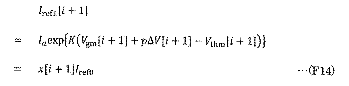
式(F13)、式(F14)より、x[i+1]は次の式で表すことができる。

そのため、式(F13)は、次の式に書き換えることができる。

つまり、セルIM[i+1,j]に含まれているトランジスタF2の第1端子−第2端子間に流れる電流は、第1データである重み係数w[i+1,j]と、第2データであるニューロンの信号の値x[i+1]と、の積に比例する。
ここで、変換回路ITRZ[j]から、トランジスタF4[j]と配線WCL[j]とを介して、セルIM[i,j]及びセルIM[i+1,j]に流れる電流の総和を考える。当該電流の総和をIS[j]とすると、IS[j]は、式(F12)と式(F16)より、次の式で表すことができる。

したがって、変換回路ITRZ[j]から出力される電流は、第1データである重み係数w[i,j]及びw[i+1,j]と、第2データであるニューロンの信号の値x[i]及びx[i+1]と、の積和に比例した電流となる。
なお、上述の動作例では、セルIM[i,j]、及びセルIM[i+1,j]に流れる電流の総和について扱ったが、複数のセルとして、セルIM[1,j]乃至セルIM[m,j]のそれぞれに流れる電流の総和についても扱ってもよい。この場合、式(F17)は、次の式に書き直すことができる。

このため、3行以上且つ2列以上のセルアレイCA2を有する演算回路MAC2の場合でも、上記の通り、積和演算を行うことができる。この場合の積和演算回路は、複数列のうち1列を、電流量としてIref0、及びxIref0を保持するセルとすることで、複数列のうち残りの列の数だけ積和演算処理を同時に実行することができる。つまり、メモリセルアレイの列の数を増やすことで、高速な積和演算処理を実現する半導体装置を提供することができる。
本実施の形態で述べた積和演算回路を、上述した隠れ層として適用する場合、重み係数ws[k]s[k−1]
(k)を第1データとして、第1データに応じた電流量を同じ列の各セルIMに順次記憶させて、第(k−1)層の第s[k−1]ニューロンからの出力信号zs[k−1]
(k−1)を第2データとして、第2データに応じた電流を回路XCSから各行の配線XCLに対して流すことで、回路ITRZから出力される電流ISから第1データと第2データとの積和を求めることができる。加えて、当該積和の値を用いて活性化関数の値を求めることによって、活性化関数の値を信号として第k層の第s[k]ニューロンの出力信号zs[k]
(k)とすることができる。
また、本実施の形態で述べた積和演算回路を、上述した出力層として適用する場合、重み係数ws[L]s[L−1]
(L)を第1データとして、第1データに応じた電流量を同じ列の各セルIMに順次記憶させて、第(L−1)層の第s[L−1]ニューロンからの出力信号zs[L−1]
(L−1)を第2データとして、第2データに応じた電流を回路XCSから各行の配線XCLに対して流すことで、回路ITRZから出力される電流ISから、第1データと第2データとの積和を求めることができる。加えて、当該積和の値を用いて活性化関数の値を求めることによって、活性化関数の値を信号として第L層の第s[L]ニューロンの出力信号zs[L]
(L)とすることができる。
なお、本実施の形態で述べた入力層は、入力信号を第2層に出力するバッファ回路として機能してもよい。
また、本実施の形態では、演算回路MAC1及び演算回路MAC2に含まれているトランジスタをOSトランジスタ、又はSiトランジスタとした場合について説明したが、本発明の一態様は、これに限定されない。演算回路MAC1及び演算回路MAC2に含まれているトランジスタは、例えば、Ge、ZnSe、CdS、GaAs、InP、GaN、SiGe等の化合物半導体を活性層としたトランジスタ、カーボンナノチューブを活性層としたトランジスタ、有機半導体を活性層としたトランジスタ等を用いることができる。
本実施の形態に示した構成例は、互いに適宜組み合わせることができる。また、本実施の形態は、本明細書で示す他の実施の形態等と適宜組み合わせることができる。
(実施の形態4)
本実施の形態では、本発明の一態様の検査装置が有する、主記憶装置及び補助記憶装置等の記憶装置の構成例について説明する。
本実施の形態では、本発明の一態様の検査装置が有する、主記憶装置及び補助記憶装置等の記憶装置の構成例について説明する。
本発明の一態様の検査装置が有する記憶装置は、OSトランジスタ、及び容量素子を有する構成とすることができる。OSトランジスタのオフ電流は極めて小さいため、OSメモリは優れた保持特性をもち、不揮発性メモリとして機能させることができる。
<記憶装置の構成例>
図17AにOSメモリの構成の一例を示す。記憶装置1400は、周辺回路1411、及びメモリセルアレイ1470を有する。周辺回路1411は、行回路1420、列回路1430、出力回路1440、及びコントロールロジック回路1460を有する。
図17AにOSメモリの構成の一例を示す。記憶装置1400は、周辺回路1411、及びメモリセルアレイ1470を有する。周辺回路1411は、行回路1420、列回路1430、出力回路1440、及びコントロールロジック回路1460を有する。
列回路1430は、例えば、列デコーダ、プリチャージ回路、センスアンプ、書き込み回路等を有する。プリチャージ回路は、配線をプリチャージする機能を有する。センスアンプは、メモリセルから読み出されたデータ信号を増幅する機能を有する。なお、上記配線は、メモリセルアレイ1470が有するメモリセルに接続されている配線であり、詳しくは後述する。増幅されたデータ信号は、出力回路1440を介して、データ信号RDATAとして記憶装置1400の外部に出力される。また、行回路1420は、例えば、行デコーダ、ワード線ドライバ回路等を有し、アクセスする行を選択することができる。
記憶装置1400には、外部から電源電圧として低電源電圧(VSS)、周辺回路1411用の高電源電圧(VDD)、メモリセルアレイ1470用の高電源電圧(VIL)が供給される。また、記憶装置1400には、制御信号(CE、WE、RE)、アドレス信号ADDR、データ信号WDATAが外部から入力される。アドレス信号ADDRは、行デコーダ及び列デコーダに入力され、WDATAは書き込み回路に入力される。
コントロールロジック回路1460は、外部からの入力信号(CE、WE、RE)を処理して、行デコーダ、列デコーダの制御信号を生成する。CEは、チップイネーブル信号であり、WEは、書き込みイネーブル信号であり、REは、読み出しイネーブル信号である。コントロールロジック回路1460が処理する信号は、これに限定されるものではなく、必要に応じて、他の制御信号を入力すればよい。
メモリセルアレイ1470は、行列状に配置された、複数個のメモリセルMCと、複数の配線を有する。なお、メモリセルアレイ1470と行回路1420とを接続している配線の数は、メモリセルMCの構成、一列に有するメモリセルMCの数等によって決まる。また、メモリセルアレイ1470と列回路1430とを接続している配線の数は、メモリセルMCの構成、一行に有するメモリセルMCの数等によって決まる。
なお、図17Aにおいて、周辺回路1411とメモリセルアレイ1470を同一平面上に形成する例について示したが、本実施の形態はこれに限られるものではない。例えば、図17Bに示すように、周辺回路1411の一部の上に、メモリセルアレイ1470が重なるように設けられてもよい。例えば、メモリセルアレイ1470の下に重なるように、センスアンプを設ける構成にしてもよい。
図18に上述のメモリセルMCに適用できるメモリセルの構成例について説明する。
<<DOSRAM>>
図18A乃至図18Cに、DRAMのメモリセルの回路構成例を示す。本明細書等において、1OSトランジスタ1容量素子型のメモリセルを用いたDRAMを、DOSRAMと呼ぶ場合がある。図18Aに示す、メモリセル1471は、トランジスタM1と、容量素子CAと、を有する。なお、トランジスタM1は、ゲート(トップゲートと呼ぶ場合がある。)、及びバックゲートを有する。
図18A乃至図18Cに、DRAMのメモリセルの回路構成例を示す。本明細書等において、1OSトランジスタ1容量素子型のメモリセルを用いたDRAMを、DOSRAMと呼ぶ場合がある。図18Aに示す、メモリセル1471は、トランジスタM1と、容量素子CAと、を有する。なお、トランジスタM1は、ゲート(トップゲートと呼ぶ場合がある。)、及びバックゲートを有する。
トランジスタM1の第1端子は、容量素子CAの第1端子と接続され、トランジスタM1の第2端子は、配線BILと接続され、トランジスタM1のゲートは、配線WOLと接続され、トランジスタM1のバックゲートは、配線BGLと接続されている。容量素子CAの第2端子は、配線CALと接続されている。
配線BILは、ビット線として機能し、配線WOLは、ワード線として機能する。配線CALは、容量素子CAの第2端子に所定の電位を印加するための配線として機能する。データの書き込み時、及び読み出し時において、配線CALには、低レベル電位を印加するのが好ましい。配線BGLは、トランジスタM1のバックゲートに電位を印加するための配線として機能する。配線BGLに任意の電位を印加することによって、トランジスタM1のしきい値電圧を増減することができる。
また、メモリセルMCは、メモリセル1471に限定されず、回路構成の変更を行うことができる。例えば、メモリセルMCは、図18Bに示すメモリセル1472のように、トランジスタM1のバックゲートが、配線BGLでなく、配線WOLと接続される構成にしてもよい。また、例えば、メモリセルMCは、図18Cに示すメモリセル1473のように、シングルゲート構造のトランジスタ、つまりバックゲートを有さないトランジスタM1で構成されたメモリセルとしてもよい。
上記実施の形態に示す半導体装置をメモリセル1471等に用いる場合、トランジスタM1として、以降の実施の形態に示すトランジスタを用いることができる。トランジスタM1としてOSトランジスタを用いることによって、トランジスタM1のリーク電流を非常に低くすることができる。つまり、書き込んだデータをトランジスタM1によって長時間保持することができるため、メモリセルのリフレッシュの頻度を少なくすることができる。また、メモリセルのリフレッシュ動作を不要にすることができる。また、リーク電流が非常に低いため、メモリセル1471、メモリセル1472、メモリセル1473に多値データ、又はアナログデータを保持することができる。
また、DOSRAMにおいて、上記のように、メモリセルアレイ1470の下に重なるように、センスアンプを設ける構成にすると、ビット線を短くすることができる。これにより、ビット線容量が小さくなり、メモリセルの保持容量を低減することができる。
<<NOSRAM>>
図18D乃至図18Gに、2トランジスタ1容量素子のゲインセル型のメモリセルの回路構成例を示す。図18Dに示す、メモリセル1474は、トランジスタM2と、トランジスタM3と、容量素子CBと、を有する。なお、トランジスタM2は、トップゲート(単にゲートと呼ぶ場合がある。)、及びバックゲートを有する。本明細書等において、トランジスタM2にOSトランジスタを用いたゲインセル型のメモリセルを有する記憶装置を、NOSRAMと呼ぶ場合がある。
図18D乃至図18Gに、2トランジスタ1容量素子のゲインセル型のメモリセルの回路構成例を示す。図18Dに示す、メモリセル1474は、トランジスタM2と、トランジスタM3と、容量素子CBと、を有する。なお、トランジスタM2は、トップゲート(単にゲートと呼ぶ場合がある。)、及びバックゲートを有する。本明細書等において、トランジスタM2にOSトランジスタを用いたゲインセル型のメモリセルを有する記憶装置を、NOSRAMと呼ぶ場合がある。
トランジスタM2の第1端子は、容量素子CBの第1端子と接続され、トランジスタM2の第2端子は、配線WBLと接続され、トランジスタM2のゲートは、配線WOLと接続され、トランジスタM2のバックゲートは、配線BGLと接続されている。容量素子CBの第2端子は、配線CALと接続されている。トランジスタM3の第1端子は、配線RBLと接続され、トランジスタM3の第2端子は、配線SLと接続され、トランジスタM3のゲートは、容量素子CBの第1端子と接続されている。
配線WBLは、書き込みビット線として機能し、配線RBLは、読み出しビット線として機能し、配線WOLは、ワード線として機能する。配線CALは、容量素子CBの第2端子に所定の電位を印加するための配線として機能する。データの書き込み時、データ保持の最中、データの読み出し時において、配線CALには、低レベル電位を印加するのが好ましい。配線BGLは、トランジスタM2のバックゲートに電位を印加するための配線として機能する。配線BGLに任意の電位を印加することによって、トランジスタM2のしきい値電圧を増減することができる。
また、メモリセルMCは、メモリセル1474に限定されず、回路の構成を適宜変更することができる。例えば、メモリセルMCは、図18Eに示すメモリセル1475のように、トランジスタM2のバックゲートが、配線BGLでなく、配線WOLと接続される構成にしてもよい。また、例えば、メモリセルMCは、図18Fに示すメモリセル1476のように、シングルゲート構造のトランジスタ、つまりバックゲートを有さないトランジスタM2で構成されたメモリセルとしてもよい。また、例えば、メモリセルMCは、図18Gに示すメモリセル1477のように、配線WBLと配線RBLを一本の配線BILとしてまとめた構成であってもよい。
上記実施の形態に示す半導体装置をメモリセル1474等に用いる場合、トランジスタM2として以降の実施の形態に示すトランジスタを用いることができる。トランジスタM2としてOSトランジスタを用いることによって、トランジスタM2のリーク電流を非常に低くすることができる。これにより、書き込んだデータをトランジスタM2によって長時間保持することができるため、メモリセルのリフレッシュの頻度を少なくすることができる。また、メモリセルのリフレッシュ動作を不要にすることができる。また、リーク電流が非常に低いため、メモリセル1474に多値データ、又はアナログデータを保持することができる。メモリセル1475乃至1477も同様である。
なお、トランジスタM3は、チャネル形成領域にシリコンを有するトランジスタ(以下、Siトランジスタと呼ぶ場合がある)であってもよい。Siトランジスタの導電型は、nチャネル型としてもよいし、pチャネル型としてもよい。Siトランジスタは、OSトランジスタよりも電界効果移動度が高くなる場合がある。よって、読み出しトランジスタとして機能するトランジスタM3として、Siトランジスタを用いてもよい。また、トランジスタM3にSiトランジスタを用いることで、トランジスタM3の上に積層してトランジスタM2を設けることができるため、メモリセルの占有面積を低減し、記憶装置の高集積化を図ることができる。
また、トランジスタM3はOSトランジスタであってもよい。トランジスタM2及びトランジスタM3にOSトランジスタを用いた場合、メモリセルアレイ1470をn型トランジスタのみを用いて回路を構成することができる。
また、図18Hに3トランジスタ1容量素子のゲインセル型のメモリセルの一例を示す。図18Hに示すメモリセル1478は、トランジスタM4乃至トランジスタM6、及び容量素子CCを有する。容量素子CCは適宜設けられる。メモリセル1478は、配線BIL、配線RWL、配線WWL、配線BGL、及び配線GNDLに電気的に接続されている。配線GNDLは低レベル電位を与える配線である。なお、メモリセル1478を、配線BILに代えて、配線RBL、配線WBLに電気的に接続してもよい。
トランジスタM4は、バックゲートを有するOSトランジスタであり、バックゲートは配線BGLに電気的に接続されている。なお、トランジスタM4のバックゲートとゲートとを互いに電気的に接続してもよい。あるいは、トランジスタM4はバックゲートを有さなくてもよい。
なお、トランジスタM5、トランジスタM6はそれぞれ、nチャネル型Siトランジスタ又はpチャネル型Siトランジスタでもよい。或いは、トランジスタM4乃至トランジスタM6がOSトランジスタでもよい、この場合、メモリセルアレイ1470をn型トランジスタのみを用いて回路を構成することができる。
上記実施の形態に示す半導体装置をメモリセル1478に用いる場合、トランジスタM4として以降の実施の形態に示すトランジスタを用いることができる。トランジスタM4としてOSトランジスタを用いることによって、トランジスタM4のリーク電流を非常に低くすることができる。
なお、本実施の形態に示す、周辺回路1411、メモリセルアレイ1470等の構成は、上記に限定されるものではない。これらの回路、及び当該回路に接続される配線、回路素子等の、配置又は機能は、必要に応じて、変更、削除、又は追加してもよい。
本実施の形態に示した構成例は、互いに適宜組み合わせることができる。また、本実施の形態は、本明細書で示す他の実施の形態等と適宜組み合わせることができる。
(実施の形態5)
本実施の形態では、上記実施の形態で説明した演算回路の構成例、及び当該演算回路に適用可能なトランジスタの構成例について説明する。
本実施の形態では、上記実施の形態で説明した演算回路の構成例、及び当該演算回路に適用可能なトランジスタの構成例について説明する。
<半導体装置の構成例>
図19に示す半導体装置は、トランジスタ300と、トランジスタ500と、容量素子600と、を有している。図21Aはトランジスタ500のチャネル長方向の断面図であり、図21Bはトランジスタ500のチャネル幅方向の断面図であり、図21Cはトランジスタ300のチャネル幅方向の断面図である。
図19に示す半導体装置は、トランジスタ300と、トランジスタ500と、容量素子600と、を有している。図21Aはトランジスタ500のチャネル長方向の断面図であり、図21Bはトランジスタ500のチャネル幅方向の断面図であり、図21Cはトランジスタ300のチャネル幅方向の断面図である。
トランジスタ500は、チャネル形成領域に金属酸化物を有するトランジスタ(OSトランジスタ)である。トランジスタ500は、オフ電流が小さいため、これを半導体装置、例えば、演算回路MAC1等に含まれるメモリセルアレイCAのトランジスタTr11等に用いることにより、長期にわたり書き込んだデータを保持することが可能である。つまり、リフレッシュ動作の頻度が少ない、あるいは、リフレッシュ動作を必要としないため、半導体装置の消費電力を低減することができる。
本実施の形態で説明する半導体装置は、図19に示すようにトランジスタ300、トランジスタ500、容量素子600を有する。トランジスタ500はトランジスタ300の上方に設けられ、容量素子600はトランジスタ300、及びトランジスタ500の上方に設けられている。なお、容量素子600は、上記実施の形態で説明した演算回路MAC1等に含まれるメモリセルアレイCAの容量C1、回路OFSTの容量C2等とすることができる。
トランジスタ300は、基板311上に設けられる。トランジスタ300は、導電体316及び絶縁体315を有する。また、トランジスタ300は、基板311の一部からなる半導体領域313、ソース領域又はドレイン領域として機能する低抵抗領域314a、及び低抵抗領域314bを有する。なお、トランジスタ300は、例えば、上記実施の形態で説明した演算回路MAC1等に含まれるメモリセルアレイCAのトランジスタTr12等に適用することができる。
また、基板311としては、半導体基板(例えば単結晶基板又はシリコン基板)を用いるのが好ましい。
トランジスタ300は、図21Cに示すように、半導体領域313の上面及びチャネル幅方向の側面が絶縁体315を介して導電体316に覆われている。このように、トランジスタ300をFin型とすることにより、実効上のチャネル幅が増大することによりトランジスタ300のオン特性を向上させることができる。また、ゲート電極の電界の寄与を高くすることができるため、トランジスタ300のオフ特性を向上させることができる。
なお、トランジスタ300は、pチャネル型、あるいはnチャネル型のいずれでもよい。
半導体領域313のチャネルが形成される領域、その近傍の領域、ソース領域、又はドレイン領域となる低抵抗領域314a、及び低抵抗領域314b等において、シリコン系半導体等の半導体を含むことが好ましく、単結晶シリコンを含むことが好ましい。又は、Ge(ゲルマニウム)、SiGe(シリコンゲルマニウム)、GaAs(ガリウムヒ素)、GaAlAs(ガリウムアルミニウムヒ素)等を有する材料で形成してもよい。結晶格子に応力を与え、格子間隔を変化させることで有効質量を制御したシリコンを用いた構成としてもよい。又はGaAsとGaAlAs等を用いることで、トランジスタ300をHEMT(High Electron Mobility Transistor)としてもよい。
低抵抗領域314a、及び低抵抗領域314bは、半導体領域313に適用される半導体材料に加え、ヒ素、リン等のn型の導電性を付与する元素、又はホウ素等のp型の導電性を付与する元素を含む。
ゲート電極として機能する導電体316は、ヒ素、リン等のn型の導電性を付与する元素、もしくはホウ素等のp型の導電性を付与する元素を含むシリコン等の半導体材料を用いることができる。また、金属材料、合金材料、又は金属酸化物材料等の導電性材料を用いることができる。
なお、導電体の材料によって仕事関数が決まるため、当該導電体の材料を選択することで、トランジスタのしきい値電圧を調整することができる。具体的には、導電体に窒化チタンや窒化タンタル等の材料を用いることが好ましい。さらに導電性と埋め込み性を両立するために導電体にタングステンやアルミニウム等の金属材料を積層として用いることが好ましく、特にタングステンを用いることが耐熱性の点で好ましい。
図19に示すトランジスタ300の構成は一例であり、その構造に限定されず、回路構成や動作方法に応じて適切なトランジスタを用いればよい。例えば、半導体装置をOSトランジスタのみの単極性回路とする場合、図20に示すとおり、トランジスタ300の構成を、酸化物半導体を用いているトランジスタ500と同様の構成にすればよい。なお、トランジスタ500の詳細については後述する。
トランジスタ300を覆って、絶縁体320、絶縁体322、絶縁体324、及び絶縁体326が順に積層して設けられている。
絶縁体320、絶縁体322、絶縁体324、及び絶縁体326として、例えば、酸化シリコン、酸化窒化シリコン、窒化酸化シリコン、窒化シリコン、酸化アルミニウム、酸化窒化アルミニウム、窒化酸化アルミニウム、窒化アルミニウム等を用いればよい。
なお、本明細書中において、酸化窒化シリコンとは、その組成として窒素よりも酸素の含有量が多い材料を指し、窒化酸化シリコンとは、その組成として、酸素よりも窒素の含有量が多い材料を指す。また、本明細書中において、酸化窒化アルミニウムとは、その組成として窒素よりも酸素の含有量が多い材料を指し、窒化酸化アルミニウムとは、その組成として、酸素よりも窒素の含有量が多い材料を指す。
絶縁体322は、その下方に設けられるトランジスタ300等によって生じる段差を平坦化する平坦化膜としての機能を有していてもよい。例えば、絶縁体322の上面は、平坦性を高めるために化学機械研磨(CMP)法等を用いた平坦化処理により平坦化されていてもよい。
また、絶縁体324には、基板311、又はトランジスタ300等から、トランジスタ500が設けられる領域に、水素や不純物が拡散しないようなバリア性を有する膜を用いることが好ましい。
水素に対するバリア性を有する膜の一例として、例えば、CVD法で形成した窒化シリコンを用いることができる。ここで、トランジスタ500等の酸化物半導体を有する半導体素子に、水素が拡散することで、当該半導体素子の特性が低下する場合がある。したがって、トランジスタ500と、トランジスタ300との間に、水素の拡散を抑制する膜を用いることが好ましい。水素の拡散を抑制する膜とは、具体的には、水素の脱離量が少ない膜とする。
水素の脱離量は、例えば、昇温脱離ガス分析法(TDS)等を用いて分析することができる。例えば、絶縁体324の水素の脱離量は、TDS分析において、膜の表面温度が50℃から500℃の範囲において、水素原子に換算した脱離量が、絶縁体324の面積当たりに換算して、10×1015atoms/cm2以下、好ましくは5×1015atoms/cm2以下であればよい。
なお、絶縁体326は、絶縁体324よりも比誘電率が低いことが好ましい。例えば、絶縁体326の比誘電率は4未満が好ましく、3未満がより好ましい。また例えば、絶縁体326の比誘電率は、絶縁体324の比誘電率の0.7倍以下が好ましく、0.6倍以下がより好ましい。比誘電率が低い材料を層間膜とすることで、配線間に生じる寄生容量を低減することができる。
また、絶縁体320、絶縁体322、絶縁体324、及び絶縁体326には容量素子600、又はトランジスタ500と接続する導電体328、及び導電体330等が埋め込まれている。なお、導電体328、及び導電体330は、プラグ又は配線としての機能を有する。また、プラグ又は配線としての機能を有する導電体は、複数の構造をまとめて同一の符号を付与する場合がある。また、本明細書等において、配線と、配線と接続するプラグとが一体物であってもよい。すなわち、導電体の一部が配線として機能する場合、及び導電体の一部がプラグとして機能する場合もある。
各プラグ、及び配線(導電体328、導電体330等)の材料としては、金属材料、合金材料、金属窒化物材料、又は金属酸化物材料等の導電性材料を、単層又は積層して用いることができる。耐熱性と導電性を両立するタングステンやモリブデン等の高融点材料を用いることが好ましく、タングステンを用いることが好ましい。又は、アルミニウムや銅等の低抵抗導電性材料で形成することが好ましい。低抵抗導電性材料を用いることで配線抵抗を低くすることができる。
絶縁体326上、及び導電体330上に、配線層を設けてもよい。例えば、図19において、絶縁体350、絶縁体352、及び絶縁体354が順に積層して設けられている。また、絶縁体350、絶縁体352、及び絶縁体354には、導電体356が埋め込まれている。導電体356は、トランジスタ300と接続するプラグ、又は配線としての機能を有する。なお導電体356は、導電体328、及び導電体330と同様の材料を用いて設けることができる。
なお、例えば、絶縁体350は、絶縁体324と同様に、水素に対するバリア性を有する絶縁体を用いることが好ましい。また、導電体356は、水素に対するバリア性を有する導電体を含むことが好ましい。特に、水素に対するバリア性を有する絶縁体350が有する開口部に、水素に対するバリア性を有する導電体が形成される構成とすることが好ましい。当該構成により、トランジスタ300とトランジスタ500とは、バリア層により分離することができ、トランジスタ300からトランジスタ500への水素の拡散を抑制することができる。
なお、水素に対するバリア性を有する導電体としては、例えば、窒化タンタル等を用いるとよい。また、窒化タンタルと、導電性が高いタングステンとを積層することで、配線としての導電性を保持したまま、トランジスタ300からの水素の拡散を抑制することができる。この場合、水素に対するバリア性を有する窒化タンタル層が、水素に対するバリア性を有する絶縁体350と接する構造であることが好ましい。
絶縁体354上、及び導電体356上に、配線層を設けてもよい。例えば、図19において、絶縁体360、絶縁体362、及び絶縁体364が順に積層して設けられている。また、絶縁体360、絶縁体362、及び絶縁体364には、導電体366が埋め込まれている。導電体366は、プラグ又は配線としての機能を有する。なお導電体366は、導電体328、及び導電体330と同様の材料を用いて設けることができる。
なお、例えば、絶縁体360は、絶縁体324と同様に、水素に対するバリア性を有する絶縁体を用いることが好ましい。また、導電体366は、水素に対するバリア性を有する導電体を含むことが好ましい。特に、水素に対するバリア性を有する絶縁体360が有する開口部に、水素に対するバリア性を有する導電体が形成される構成とすることが好ましい。当該構成により、トランジスタ300とトランジスタ500とは、バリア層により分離することができ、トランジスタ300からトランジスタ500への水素の拡散を抑制することができる。
絶縁体364上、及び導電体366上に、配線層を設けてもよい。例えば、図19において、絶縁体370、絶縁体372、及び絶縁体374が順に積層して設けられている。また、絶縁体370、絶縁体372、及び絶縁体374には、導電体376が埋め込まれている。導電体376は、プラグ又は配線としての機能を有する。なお導電体376は、導電体328、及び導電体330と同様の材料を用いて設けることができる。
なお、例えば、絶縁体370は、絶縁体324と同様に、水素に対するバリア性を有する絶縁体を用いることが好ましい。また、導電体376は、水素に対するバリア性を有する導電体を含むことが好ましい。特に、水素に対するバリア性を有する絶縁体370が有する開口部に、水素に対するバリア性を有する導電体が形成される構成とすることが好ましい。当該構成により、トランジスタ300とトランジスタ500とは、バリア層により分離することができ、トランジスタ300からトランジスタ500への水素の拡散を抑制することができる。
絶縁体374上、及び導電体376上に、配線層を設けてもよい。例えば、図19において、絶縁体380、絶縁体382、及び絶縁体384が順に積層して設けられている。また、絶縁体380、絶縁体382、及び絶縁体384には、導電体386が埋め込まれている。導電体386は、プラグ又は配線としての機能を有する。なお導電体386は、導電体328、及び導電体330と同様の材料を用いて設けることができる。
なお、例えば、絶縁体380は、絶縁体324と同様に、水素に対するバリア性を有する絶縁体を用いることが好ましい。また、導電体386は、水素に対するバリア性を有する導電体を含むことが好ましい。特に、水素に対するバリア性を有する絶縁体380が有する開口部に、水素に対するバリア性を有する導電体が形成される構成とすることが好ましい。当該構成により、トランジスタ300とトランジスタ500とは、バリア層により分離することができ、トランジスタ300からトランジスタ500への水素の拡散を抑制することができる。
導電体366、導電体376、および導電体386は、導電体356と同様の構成とすることができる。
上記において、本発明の一態様の半導体装置が導電体356を含む配線層と、導電体366を含む配線層と、導電体376を含む配線層と、導電体386を含む配線層を有するとしたが、本発明の一態様の半導体装置はこれに限らない。導電体356を含む配線層と同様の配線層を3層以下にしてもよいし、導電体356を含む配線層と同様の配線層を5層以上にしてもよい。
絶縁体384上には絶縁体510、絶縁体512、絶縁体514、及び絶縁体516が、順に積層して設けられている。絶縁体510、絶縁体512、絶縁体514、及び絶縁体516のいずれかは、酸素や水素に対してバリア性のある物質を用いることが好ましい。
例えば、絶縁体510、及び絶縁体514には、基板311、又はトランジスタ300を設ける領域等から、トランジスタ500を設ける領域に、水素や不純物が拡散しないようなバリア性を有する膜用いることが好ましい。したがって、絶縁体324と同様の材料を用いることができる。
水素に対するバリア性を有する膜の一例として、CVD法で形成した窒化シリコンを用いることができる。ここで、トランジスタ500等の酸化物半導体を有する半導体素子に、水素が拡散することで、当該半導体素子の特性が低下する場合がある。したがって、トランジスタ500と、トランジスタ300との間に、水素の拡散を抑制する膜を用いることが好ましい。水素の拡散を抑制する膜とは、具体的には、水素の脱離量が少ない膜とする。
また、水素に対するバリア性を有する膜として、例えば、絶縁体510、及び絶縁体514には、酸化アルミニウム、酸化ハフニウム、酸化タンタル等の金属酸化物を用いることが好ましい。
特に、酸化アルミニウムは、酸素と、トランジスタの電気特性の変動要因となる水素、水分等の不純物と、の両方に対して膜を透過させない遮断効果が高い。したがって、酸化アルミニウムは、トランジスタの作製工程中及び作製後において、水素、水分等の不純物のトランジスタ500への混入を防止することができる。また、トランジスタ500を構成する酸化物からの酸素の放出を抑制することができる。そのため、トランジスタ500に対する保護膜として用いることに適している。
また、例えば、絶縁体512、及び絶縁体516には、絶縁体320と同様の材料を用いることができる。また、これらの絶縁体に、比較的誘電率が低い材料を適用することで、配線間に生じる寄生容量を低減することができる。例えば、絶縁体512、及び絶縁体516として、酸化シリコン膜や酸化窒化シリコン膜等を用いることができる。
また、絶縁体510、絶縁体512、絶縁体514、及び絶縁体516には、導電体518、及びトランジスタ500を構成する導電体(例えば、導電体503)等が埋め込まれている。なお、導電体518は、容量素子600、又はトランジスタ300と接続するプラグ、又は配線としての機能を有する。導電体518は、導電体328、及び導電体330と同様の材料を用いて設けることができる。
特に、絶縁体510、及び絶縁体514と接する領域の導電体518は、酸素、水素、及び水に対するバリア性を有する導電体であることが好ましい。当該構成により、トランジスタ300とトランジスタ500とは、酸素、水素、及び水に対するバリア性を有する層で、分離することができ、トランジスタ300からトランジスタ500への水素の拡散を抑制することができる。
絶縁体516の上方には、トランジスタ500が設けられている。
図21A及び図21Bに示すように、トランジスタ500は、絶縁体514及び絶縁体516に埋め込まれるように配置された導電体503と、絶縁体516及び導電体503の上に配置された絶縁体520と、絶縁体520の上に配置された絶縁体522と、絶縁体522の上に配置された絶縁体524と、絶縁体524の上に配置された酸化物530aと、酸化物530aの上に配置された酸化物530bと、酸化物530b上に互いに離れて配置された導電体542a及び導電体542bと、導電体542a及び導電体542b上に配置され、導電体542aと導電体542bの間に重畳して開口が形成された絶縁体580と、開口の底面及び側面と接する領域を有するように配置された酸化物530cと、酸化物530cの形成面に配置された絶縁体550と、絶縁体550の形成面に配置された導電体560と、を有する。
また、図21A及び図21Bに示すように、酸化物530a、酸化物530b、導電体542a、及び導電体542bと、絶縁体580との間に絶縁体544が配置されることが好ましい。また、図21A及び図21Bに示すように、導電体560は、絶縁体550の内側に設けられた導電体560aと、導電体560aの内側に埋め込まれるように設けられた導電体560bと、を有することが好ましい。また、図21A及び図21Bに示すように、絶縁体580、導電体560、及び絶縁体550の上に絶縁体574が配置されることが好ましい。
なお、以下において、酸化物530a、酸化物530b、及び酸化物530cをまとめて酸化物530という場合がある。
なお、トランジスタ500では、チャネルが形成される領域と、その近傍において、酸化物530a、酸化物530b、及び酸化物530cの3層を積層する構成について示しているが、本発明の一態様はこれに限られるものではない。例えば、酸化物530bの単層、酸化物530bと酸化物530aの2層構造、酸化物530bと酸化物530cの2層構造、又は4層以上の積層構造を設ける構成にしてもよい。また、トランジスタ500では、導電体560を2層の積層構造として示しているが、本発明の一態様はこれに限られるものではない。例えば、導電体560が、単層構造であってもよいし、3層以上の積層構造であってもよい。また、図19、図20、図21A及び図21Bに示すトランジスタ500の構成は一例であり、その構造に限定されず、回路構成や動作方法に応じて適切なトランジスタを用いればよい。
ここで、導電体560は、トランジスタのゲート電極として機能し、導電体542a及び導電体542bは、それぞれソース電極又はドレイン電極として機能する。上記のように、導電体560は、絶縁体580の開口、及び導電体542aと導電体542bに挟まれた領域に埋め込まれるように形成される。導電体560、導電体542a及び導電体542bの配置は、絶縁体580の開口に対して、自己整合的に選択される。つまり、トランジスタ500において、ゲート電極を、ソース電極とドレイン電極の間に、自己整合的に配置させることができる。よって、導電体560を位置合わせのマージンを設けることなく形成することができるため、トランジスタ500の占有面積の縮小を図ることができる。これにより、半導体装置の微細化、高集積化を図ることができる。
さらに、導電体560が、導電体542aと導電体542bの間の領域に自己整合的に形成されるため、導電体560は、導電体542a又は導電体542bと重畳する領域を有さない。これにより、導電体560と導電体542a及び導電体542bとの間に形成される寄生容量を低減することができる。よって、トランジスタ500のスイッチング速度を向上させ、周波数特性を高めることができる。
導電体560は、第1のゲート(トップゲートともいう)電極として機能する場合がある。また、導電体503は、第2のゲート(ボトムゲートともいう)電極として機能する場合がある。その場合、導電体503に印加する電位を、導電体560に印加する電位と、連動させず、独立して変化させることで、トランジスタ500のしきい値電圧を制御することができる。特に、導電体503に負の電位を印加することにより、トランジスタ500のしきい値電圧を0Vより大きくし、オフ電流を低減することが可能となる。したがって、導電体503に負の電位を印加したほうが、印加しない場合よりも、導電体560に印加する電位が0Vのときのドレイン電流を小さくすることができる。
導電体503は、酸化物530、及び導電体560と重なるように配置する。これにより、導電体560、及び導電体503に電位を印加した場合、導電体560から生じる電界と、導電体503から生じる電界と、がつながり、酸化物530に形成されるチャネル形成領域を覆うことができる。本明細書等において、第1のゲート電極、及び第2のゲート電極の電界によって、チャネル形成領域を電気的に取り囲むトランジスタの構造を、surrounded channel(s−channel)構造とよぶ。
また、導電体503は、導電体518と同様の構成であり、絶縁体514及び絶縁体516の開口の内壁に接して導電体503aが形成され、さらに内側に導電体503bが形成されている。なお、トランジスタ500では、導電体503a及び導電体503bを積層する構成について示しているが、本発明の一態様はこれに限られるものではない。例えば、導電体503は、単層、又は3層以上の積層構造として設ける構成にしてもよい。
ここで、導電体503aは、水素原子、水素分子、水分子、銅原子等の不純物の拡散を抑制する機能を有する(上記不純物が透過しにくい。)導電性材料を用いることが好ましい。又は、酸素(例えば、酸素原子、酸素分子等の少なくとも一)の拡散を抑制する機能を有する(上記酸素が透過しにくい。)導電性材料を用いることが好ましい。なお、本明細書において、不純物、又は酸素の拡散を抑制する機能とは、上記不純物、又は上記酸素のいずれか一又は、全ての拡散を抑制する機能とする。
例えば、導電体503aが酸素の拡散を抑制する機能を持つことにより、導電体503bが酸化して導電率が低下することを抑制することができる。
また、導電体503が配線の機能を兼ねる場合、導電体503bは、タングステン、銅、又はアルミニウムを主成分とする、導電性が高い導電性材料を用いることが好ましい。その場合、導電体503aは、必ずしも設けなくともよい。なお、導電体503bを単層で図示したが、積層構造としてもよく、例えば、チタン又は窒化チタンと上記導電性材料との積層としてもよい。
絶縁体520、絶縁体522、及び絶縁体524は、導電体503に対するゲート絶縁膜としての機能を有する。
ここで、酸化物530と接する絶縁体524は、化学量論的組成を満たす酸素よりも多くの酸素を含む絶縁体を用いることが好ましい。つまり、絶縁体524には、過剰酸素領域が形成されていることが好ましい。このような過剰酸素を含む絶縁体を酸化物530に接して設けることにより、酸化物530中の酸素欠損を低減し、トランジスタ500の信頼性を向上させることができる。
過剰酸素領域を有する絶縁体として、具体的には、加熱により一部の酸素が脱離する酸化物材料を用いることが好ましい。加熱により酸素を脱離する酸化物とは、TDS(Thermal Desorption Spectroscopy)分析にて、酸素原子に換算しての酸素の脱離量が1.0×10¹⁸atoms/cm3以上、好ましくは1.0×1019atoms/cm3以上、さらに好ましくは2.0×1019atoms/cm3以上、又は3.0×1020atoms/cm3以上である酸化物膜である。なお、上記TDS分析時における膜の表面温度としては100℃以上700℃以下、又は100℃以上400℃以下の範囲が好ましい。
また、上記過剰酸素領域を有する絶縁体と、酸化物530と、を接して加熱処理、マイクロ波処理、又はRF処理のいずれか一又は複数の処理を行ってもよい。当該処理を行うことで、酸化物530中の水、又は水素を除去することができる。例えば、酸化物530において、VoHの結合が切断される反応が起きる、別言すると「VOH→VO+H」という反応が起きて、脱水素化することができる。このとき発生した水素の一部は、酸素と結合してH2Oとして、酸化物530、又は酸化物530近傍の絶縁体から除去される場合がある。また、水素の一部は、導電体542a又は導電体542bに拡散又は捕獲(ゲッタリングともいう)される場合がある。
また、上記マイクロ波処理は、例えば、高密度プラズマを発生させる電源を有する装置、又は、基板側にRFを印加する電源を有する装置を用いると好適である。例えば、酸素を含むガスを用い、且つ高密度プラズマを用いることより、高密度の酸素ラジカルを生成することができる。そして、基板側にRFを印加することで、高密度プラズマによって生成された酸素ラジカルを、効率良く酸化物530、又は酸化物530近傍の絶縁体中に導入することができる。また、上記マイクロ波処理は、圧力を133Pa以上、好ましくは200Pa以上、さらに好ましくは400Pa以上とすればよい。また、マイクロ波処理を行う装置内に導入するガスとしては、例えば、酸素と、アルゴンとを用い、酸素流量比(O2/(O2+Ar))が50%以下、好ましくは10%以上30%以下で行うとよい。
また、トランジスタ500の作製工程中において、酸化物530の表面が露出した状態で、加熱処理を行うと好適である。当該加熱処理は、例えば、100℃以上450℃以下、より好ましくは350℃以上400℃以下で行えばよい。なお、加熱処理は、窒素ガスもしくは不活性ガスの雰囲気、又は酸化性ガスを10ppm以上、1%以上、もしくは10%以上含む雰囲気で行う。例えば、加熱処理は酸素雰囲気で行うことが好ましい。これにより、酸化物530に酸素を供給して、酸素欠損(VO)の低減を図ることができる。また、加熱処理は減圧状態で行ってもよい。又は、加熱処理は、窒素ガスもしくは不活性ガスの雰囲気で加熱処理した後に、脱離した酸素を補うために、酸化性ガスを10ppm以上、1%以上、又は10%以上含む雰囲気で行ってもよい。又は、酸化性ガスを10ppm以上、1%以上、又は10%以上含む雰囲気で加熱処理した後に、連続して窒素ガスもしくは不活性ガスの雰囲気で加熱処理を行ってもよい。
なお、酸化物530に加酸素化処理を行うことで、酸化物530中の酸素欠損を、供給された酸素により修復させる、別言すると「VO+O→null」という反応を促進させることができる。さらに、酸化物530中に残存した水素に供給された酸素が反応することで、当該水素をH2Oとして除去する(脱水化する)ことができる。これにより、酸化物530中に残存していた水素が酸素欠損に再結合してVOHが形成されることを抑制することができる。
また、絶縁体524が、過剰酸素領域を有する場合、絶縁体522は、酸素(例えば、酸素原子、酸素分子等)の拡散を抑制する機能を有する(上記酸素が透過しにくい)ことが好ましい。
絶縁体522が、酸素や不純物の拡散を抑制する機能を有すると、酸化物530が有する酸素は、絶縁体520側へ拡散することがないため好ましい。また、導電体503が、絶縁体524や、酸化物530が有する酸素と反応することを抑制することができるため好ましい。
絶縁体522は、例えば、酸化アルミニウム、酸化ハフニウム、アルミニウム及びハフニウムを含む酸化物(ハフニウムアルミネート)、酸化タンタル、酸化ジルコニウム、チタン酸ジルコン酸鉛(PZT)、チタン酸ストロンチウム(SrTiO3)、又は(Ba,Sr)TiO3(BST)等のいわゆるhigh−k材料(高い比誘電率の材料)を含む絶縁体を単層又は積層で用いることが好ましい。トランジスタの微細化、及び高集積化が進むと、ゲート絶縁膜の薄膜化により、リーク電流等の問題が生じる場合がある。ゲート絶縁膜として機能する絶縁体にhigh−k材料を用いることで、物理膜厚を保ちながら、トランジスタ動作時のゲート電位の低減が可能となる。
特に、不純物、及び酸素等の拡散を抑制する機能を有する(上記酸素が透過しにくい)絶縁性材料であるアルミニウム、ハフニウムの一方又は双方の酸化物を含む絶縁体を用いるとよい。アルミニウム、ハフニウムの一方又は双方の酸化物を含む絶縁体として、酸化アルミニウム、酸化ハフニウム、アルミニウム及びハフニウムを含む酸化物(ハフニウムアルミネート)等を用いることが好ましい。このような材料を用いて絶縁体522を形成した場合、絶縁体522は、酸化物530からの酸素の放出や、トランジスタ500の周辺部から酸化物530への水素等の不純物の混入を抑制する層として機能する。
又は、これらの絶縁体に、例えば、酸化アルミニウム、酸化ビスマス、酸化ゲルマニウム、酸化ニオブ、酸化シリコン、酸化チタン、酸化タングステン、酸化イットリウム、酸化ジルコニウムを添加してもよい。又はこれらの絶縁体を窒化処理してもよい。上記の絶縁体に酸化シリコン、酸化窒化シリコン又は窒化シリコンを積層して用いてもよい。
また、絶縁体520は、熱的に安定していることが好ましい。例えば、酸化シリコン及び酸化窒化シリコンは、熱的に安定であるため、好適である。また、high−k材料の絶縁体と、酸化シリコン又は酸化窒化シリコンと、を組み合わせることで、熱的に安定かつ比誘電率の高い積層構造の絶縁体520を取得することができる。
なお、図21A及び図21Bのトランジスタ500では、導電体503に対する、3層の積層構造からなるゲート絶縁膜として、絶縁体520、絶縁体522、及び絶縁体524が図示されているが、当該ゲート絶縁膜は、単層、2層、又は4層以上の積層構造を有していてもよい。その場合、同じ材料からなる積層構造に限定されず、異なる材料からなる積層構造でもよい。
トランジスタ500は、チャネル形成領域を含む酸化物530に、酸化物半導体として機能する金属酸化物を用いることが好ましい。例えば、酸化物530として、In−M−Zn酸化物(元素Mは、アルミニウム、ガリウム、イットリウム、銅、バナジウム、ベリリウム、ホウ素、チタン、鉄、ニッケル、ゲルマニウム、ジルコニウム、モリブデン、ランタン、セリウム、ネオジム、ハフニウム、タンタル、タングステン、又はマグネシウム等から選ばれた一種、又は複数種)等の金属酸化物を用いるとよい。特に、酸化物530として適用できるIn−M−Zn酸化物は、CAAC−OS(C−Axis Aligned Crystalline Oxide Semiconductor)、CAC−OS(Cloud−Aligned Composite Oxide Semiconductor)であることが好ましい。また、酸化物530として、In−Ga酸化物、In−Zn酸化物、In酸化物等を用いてもよい。
また、トランジスタ500には、キャリア濃度の低い金属酸化物を用いることが好ましい。金属酸化物のキャリア濃度を低くするためには、金属酸化物中の不純物濃度を低くし、欠陥準位密度を低くすればよい。本明細書等において、不純物濃度が低く、欠陥準位密度が低いことを高純度真性、又は実質的に高純度真性という。なお、金属酸化物中の不純物としては、例えば、水素、窒素、アルカリ金属、アルカリ土類金属、鉄、ニッケル、シリコン等がある。
特に、金属酸化物に含まれる水素は、金属原子と結合する酸素と反応して水になるため、金属酸化物中に酸素欠損を形成する場合がある。また、酸化物530中の酸素欠損に水素が入った場合、酸素欠損と水素とが結合しVOHを形成する場合がある。VOHはドナーとして機能し、キャリアである電子が生成されることがある。また、水素の一部が金属原子と結合する酸素と結合して、キャリアである電子を生成する場合がある。従って、水素が多く含まれている金属酸化物を用いたトランジスタは、ノーマリーオン特性となりやすい。また、金属酸化物中の水素は、熱、電界等のストレスによって動きやすいため、金属酸化物に多くの水素が含まれると、トランジスタの信頼性が悪化する恐れもある。本発明の一態様においては、酸化物530中のVOHをできる限り低減し、高純度真性又は実質的に高純度真性にすることが好ましい。このように、VoHが十分低減された金属酸化物を取得するには、金属酸化物中の水分、水素等の不純物を除去すること(脱水、脱水素化処理と記載する場合がある。)と、金属酸化物に酸素を供給して酸素欠損を補填すること(加酸素化処理と記載する場合がある。)が重要である。VOH等の不純物が十分に低減された金属酸化物をトランジスタのチャネル形成領域に用いることで、安定した電気特性を付与することができる。
酸素欠損に水素が入った欠陥は、金属酸化物のドナーとして機能しうる。しかしながら、当該欠陥を定量的に評価することは困難である。そこで、金属酸化物においては、ドナー濃度ではなく、キャリア濃度で評価される場合がある。よって、本明細書等では、金属酸化物のパラメータとして、ドナー濃度ではなく、電界が印加されない状態を想定したキャリア濃度を用いる場合がある。つまり、本明細書等に記載の「キャリア濃度」は、「ドナー濃度」と言い換えることができる場合がある。
よって、金属酸化物を酸化物530に用いる場合、金属酸化物中の水素はできる限り低減されていることが好ましい。具体的には、金属酸化物において、二次イオン質量分析法(SIMS:Secondary Ion Mass Spectrometry)により取得される水素濃度を、1×10²⁰atoms/cm3未満、好ましくは1×1019atoms/cm3未満、より好ましくは5×1018atoms/cm3未満、さらに好ましくは1×1018atoms/cm3未満とする。水素等の不純物が十分に低減された金属酸化物をトランジスタのチャネル形成領域に用いることで、安定した電気特性を付与することができる。
また、酸化物530に金属酸化物を用いる場合、当該金属酸化物は、バンドギャップが高く、真性(I型ともいう。)、又は実質的に真性である半導体であって、かつチャネル形成領域の金属酸化物のキャリア濃度は、1×1018cm−3未満であることが好ましく、1×1017cm−3未満であることがより好ましく、1×1016cm−3未満であることがさらに好ましく、1×1013cm−3未満であることがさらに好ましく、1×1012cm−3未満であることがさらに好ましい。なお、チャネル形成領域の金属酸化物のキャリア濃度の下限値については、特に限定は無いが、例えば、1×10⁻⁹cm−3とすることができる。
また、酸化物530に金属酸化物を用いる場合、導電体542a及び導電体542bと酸化物530とが接することで、酸化物530中の酸素が導電体542a及び導電体542bへ拡散し、導電体542a及び導電体542bが酸化する場合がある。導電体542a及び導電体542bが酸化することで、導電体542a及び導電体542bの導電率が低下する蓋然性が高い。なお、酸化物530中の酸素が導電体542a及び導電体542bへ拡散することを、導電体542a及び導電体542bが酸化物530中の酸素を吸収する、と言い換えることができる。
また、酸化物530中の酸素が導電体542a及び導電体542bへ拡散することで、導電体542aと酸化物530bとの間、及び、導電体542bと酸化物530bとの間に異層が形成される場合がある。当該異層は、導電体542a及び導電体542bよりも酸素を多く含むため、当該異層は絶縁性を有すると推定される。このとき、導電体542a又は導電体542bと、当該異層と、酸化物530bとの3層構造は、金属−絶縁体−半導体からなる3層構造とみなすことができ、MIS(Metal−Insulator−Semiconductor)構造と呼ぶ、又はMIS構造を主としたダイオード接合構造と呼ぶ場合がある。
なお、上記異層は、導電体542a及び導電体542bと酸化物530bとの間に形成されることに限られず、例えば、異層が、導電体542a及び導電体542bと酸化物530cとの間に形成される場合や、導電体542a及び導電体542bと酸化物530bとの間、導電体542a及び導電体542bと酸化物530cとの間に形成される場合がある。
酸化物530においてチャネル形成領域として機能する金属酸化物は、バンドギャップが2eV以上のものを用いることが好ましく、2.5eV以上のものを用いることがより好ましい。このように、バンドギャップの大きい金属酸化物を用いることで、トランジスタのオフ電流を低減することができる。
酸化物530は、酸化物530b下に酸化物530aを有することで、酸化物530aよりも下方に形成された構造物から、酸化物530bへの不純物の拡散を抑制することができる。また、酸化物530b上に酸化物530cを有することで、酸化物530cよりも上方に形成された構造物から、酸化物530bへの不純物の拡散を抑制することができる。
なお、酸化物530は、各金属原子の原子数比が異なる複数の酸化物層の積層構造を有することが好ましい。具体的には、酸化物530aに用いる金属酸化物において、構成元素中の元素Mの原子数比が、酸化物530bに用いる金属酸化物における、構成元素中の元素Mの原子数比より、大きいことが好ましい。また、酸化物530aに用いる金属酸化物において、Inに対する元素Mの原子数比が、酸化物530bに用いる金属酸化物における、Inに対する元素Mの原子数比より大きいことが好ましい。また、酸化物530bに用いる金属酸化物において、元素Mに対するInの原子数比が、酸化物530aに用いる金属酸化物における、元素Mに対するInの原子数比より大きいことが好ましい。また、酸化物530cは、酸化物530a又は酸化物530bに用いることができる金属酸化物を、用いることができる。
具体的には、酸化物530aとして、InとGaとZnとの原子数比がIn:Ga:Zn=1:3:4、又は1:1:0.5の金属酸化物を用いればよい。また、酸化物530bとして、InとGaとZnとの原子数比がIn:Ga:Zn=4:2:3、又は1:1:1の金属酸化物を用いればよい。また、酸化物530cとして、InとGaとZnとの原子数比がIn:Ga:Zn=1:3:4、またGaとZnの原子数比がGa:Zn=2:1、又はGa:Zn=2:5の金属酸化物を用いればよい。また、酸化物530cを積層構造とする場合の具体例としては、InとGaとZnとの原子数比がIn:Ga:Zn=4:2:3と、In:Ga:Zn=1:3:4との積層構造、またGaとZnの原子数比がGa:Zn=2:1と、InとGaとZnとの原子数比がIn:Ga:Zn=4:2:3との積層構造、GaとZnの原子数比がGa:Zn=2:5と、InとGaとZnとの原子数比がIn:Ga:Zn=4:2:3との積層構造、酸化ガリウムと、InとGaとZnとの原子数比がIn:Ga:Zn=4:2:3との積層構造等が挙げられる。
また、例えば、酸化物530aに用いる金属酸化物における元素Mに対するInの原子数比が、酸化物530bに用いる金属酸化物における元素Mに対するInの原子数比より小さい場合、酸化物530bとして、InとGaとZnとの原子数比がIn:Ga:Zn=5:1:6又はその近傍、In:Ga:Zn=5:1:3又はその近傍、In:Ga:Zn=10:1:3又はその近傍等の組成であるIn−Ga−Zn酸化物を用いることができる。
また、上述した以外の組成としては、酸化物530bには、例えば、In:Zn=2:1の組成、In:Zn=5:1の組成、In:Zn=10:1の組成、これらのいずれか一の近傍の組成等を有する金属酸化物を用いることができる。
これらの酸化物530a、酸化物530b、酸化物530cを上記の原子数比の関係を満たして組み合わせることが好ましい。例えば、酸化物530a、及び酸化物530cを、In:Ga:Zn=1:3:4の組成及びその近傍の組成を有する金属酸化物、酸化物530bを、In:Ga:Zn=4:2:3から4.1の組成及びその近傍の組成を有する金属酸化物とするのが好ましい。なお、上記組成は、基体上に形成された酸化物中の原子数比、又はスパッタターゲットにおける原子数比を示す。また、酸化物530bの組成として、Inの比率を高めることで、トランジスタのオン電流、又は電界効果移動度等を高めることが出来るため好適である。
また、酸化物530a及び酸化物530cの伝導帯下端のエネルギーが、酸化物530bの伝導帯下端のエネルギーより高くなることが好ましい。言い換えると、酸化物530a及び酸化物530cの電子親和力が、酸化物530bの電子親和力より小さいことが好ましい。
ここで、酸化物530a、酸化物530b、及び酸化物530cの接合部において、伝導帯下端のエネルギー準位はなだらかに変化する。言い換えると、酸化物530a、酸化物530b、及び酸化物530cの接合部における伝導帯下端のエネルギー準位は、連続的に変化又は連続接合するともいうことができる。このようにするためには、酸化物530aと酸化物530bとの界面、及び酸化物530bと酸化物530cとの界面において形成される混合層の欠陥準位密度を低くするとよい。
具体的には、酸化物530aと酸化物530b、酸化物530bと酸化物530cが、酸素以外に共通の元素を有する(主成分とする)ことで、欠陥準位密度が低い混合層を形成することができる。例えば、酸化物530bがIn−Ga−Zn酸化物の場合、酸化物530a及び酸化物530cとして、In−Ga−Zn酸化物、Ga−Zn酸化物、酸化ガリウム等を用いるとよい。
このとき、キャリアの主たる経路は酸化物530bとなる。酸化物530a、酸化物530cを上述の構成とすることで、酸化物530aと酸化物530bとの界面、及び酸化物530bと酸化物530cとの界面における欠陥準位密度を低くすることができる。そのため、界面散乱によるキャリア伝導への影響が小さくなり、トランジスタ500は高いオン電流を取得される。
酸化物530b上には、ソース電極、及びドレイン電極として機能する導電体542a、及び導電体542bが設けられる。導電体542a、及び導電体542bとしては、アルミニウム、クロム、銅、銀、金、白金、タンタル、ニッケル、チタン、モリブデン、タングステン、ハフニウム、バナジウム、ニオブ、マンガン、マグネシウム、ジルコニウム、ベリリウム、インジウム、ルテニウム、イリジウム、ストロンチウム、ランタンから選ばれた金属元素、又は上述した金属元素を成分とする合金か、上述した金属元素を組み合わせた合金等を用いることが好ましい。例えば、窒化タンタル、窒化チタン、タングステン、チタンとアルミニウムを含む窒化物、タンタルとアルミニウムを含む窒化物、酸化ルテニウム、窒化ルテニウム、ストロンチウムとルテニウムを含む酸化物、ランタンとニッケルを含む酸化物等を用いることが好ましい。また、窒化タンタル、窒化チタン、チタンとアルミニウムを含む窒化物、タンタルとアルミニウムを含む窒化物、酸化ルテニウム、窒化ルテニウム、ストロンチウムとルテニウムを含む酸化物、ランタンとニッケルを含む酸化物は、酸化しにくい導電性材料、又は、酸素を吸収しても導電性を維持する材料であるため、好ましい。更に、窒化タンタル等の金属窒化物膜は、水素又は酸素に対するバリア性があるため好ましい。
また、図21A、図21Bでは、導電体542a、及び導電体542bを単層構造として示したが、2層以上の積層構造としてもよい。例えば、窒化タンタル膜とタングステン膜を積層するとよい。また、チタン膜とアルミニウム膜を積層してもよい。また、タングステン膜上にアルミニウム膜を積層する二層構造、銅−マグネシウム−アルミニウム合金膜上に銅膜を積層する二層構造、チタン膜上に銅膜を積層する二層構造、タングステン膜上に銅膜を積層する二層構造としてもよい。
また、チタン膜又は窒化チタン膜と、そのチタン膜又は窒化チタン膜上に重ねてアルミニウム膜又は銅膜を積層し、さらにその上にチタン膜又は窒化チタン膜を形成する三層構造、モリブデン膜又は窒化モリブデン膜と、そのモリブデン膜又は窒化モリブデン膜上に重ねてアルミニウム膜又は銅膜を積層し、さらにその上にモリブデン膜又は窒化モリブデン膜を形成する三層構造等がある。なお、酸化インジウム、酸化錫又は酸化亜鉛を含む透明導電材料を用いてもよい。
また、図21Aに示すように、酸化物530の、導電体542a(導電体542b)との界面とその近傍には、低抵抗領域として、領域543a、及び領域543bが形成される場合がある。このとき、領域543aはソース領域又はドレイン領域の一方として機能し、領域543bはソース領域又はドレイン領域の他方として機能する。また、領域543aと領域543bに挟まれる領域にチャネル形成領域が形成される。
酸化物530と接するように上記導電体542a(導電体542b)を設けることで、領域543a(領域543b)の酸素濃度が低減する場合がある。また、導電体542a(導電体542b)に含まれる金属と、酸化物530の成分と、を含む金属化合物層が領域543a(領域543b)に形成される場合がある。このような場合、領域543a(領域543b)のキャリア濃度が増加し、領域543a(領域543b)は、低抵抗領域となる。
絶縁体544は、導電体542a、及び導電体542bを覆うように設けられ、導電体542a、及び導電体542bの酸化を抑制する。このとき、絶縁体544は、酸化物530の側面を覆い、絶縁体524と接するように設けられてもよい。
絶縁体544として、ハフニウム、アルミニウム、ガリウム、イットリウム、ジルコニウム、タングステン、チタン、タンタル、ニッケル、ゲルマニウム、ネオジム、ランタン又は、マグネシウム等から選ばれた一種、又は二種以上が含まれた金属酸化物を用いることができる。また、絶縁体544として、窒化酸化シリコン又は窒化シリコン等も用いることができる。
特に、絶縁体544として、アルミニウム又はハフニウムの酸化物を含む絶縁体である、酸化アルミニウム、又は酸化ハフニウムを用いることが好ましい。又は、アルミニウム及びハフニウムを含む酸化物(ハフニウムアルミネート)等を用いることが好ましい。特に、ハフニウムアルミネートは、酸化ハフニウム膜よりも、耐熱性が高い。そのため、後の工程での熱処理において、結晶化しにくいため好ましい。なお、導電体542a及び導電体542bが耐酸化性を有する材料である場合、又は、酸素を吸収しても導電性が著しくは低下しない材料である場合は、絶縁体544は必須の構成ではない。求めるトランジスタ特性により、適宜設計すればよい。
絶縁体544を有することで、絶縁体580に含まれる水、及び水素等の不純物が酸化物530bに拡散することを抑制することができる。また、絶縁体580が有する過剰酸素により、導電体560が酸化することを抑制することができる。
絶縁体550は、導電体560に対するゲート絶縁膜として機能する。絶縁体550は、酸化物530cの内側(上面、及び側面)に接して配置することが好ましい。絶縁体550は、上述した絶縁体524と同様に、過剰に酸素を含み、かつ加熱により酸素が放出される絶縁体を用いて形成することが好ましい。
具体的には、過剰酸素を有する酸化シリコン、酸化窒化シリコン、窒化酸化シリコン、窒化シリコン、フッ素を添加した酸化シリコン、炭素を添加した酸化シリコン、炭素、及び窒素を添加した酸化シリコン、空孔を有する酸化シリコンを用いることができる。特に、酸化シリコン、及び酸化窒化シリコンは熱に対し安定であるため好ましい。
加熱により酸素が放出される絶縁体を、絶縁体550として、酸化物530cの上面に接して設けることにより、絶縁体550から、酸化物530cを通じて、酸化物530bのチャネル形成領域に効果的に酸素を供給することができる。また、絶縁体524と同様に、絶縁体550中の水又は水素等の不純物濃度が低減されていることが好ましい。絶縁体550の膜厚は、1nm以上20nm以下とするのが好ましい。
また、絶縁体550が有する過剰酸素を、効率的に酸化物530へ供給するために、絶縁体550と導電体560との間に金属酸化物を設けてもよい。当該金属酸化物は、絶縁体550から導電体560への酸素拡散を抑制する機能を有することが好ましい。酸素の拡散を抑制する金属酸化物を設けることで、絶縁体550から導電体560への過剰酸素の拡散が抑制される。つまり、酸化物530へ供給する過剰酸素量の減少を抑制することができる。また、過剰酸素による導電体560の酸化を抑制することができる。当該金属酸化物としては、絶縁体544に用いることができる材料を用いればよい。
なお、絶縁体550は、導電体503に対するゲート絶縁膜と同様に、積層構造としてもよい。トランジスタの微細化、及び高集積化が進むと、ゲート絶縁膜の薄膜化により、リーク電流等の問題が生じる場合がある。このため、ゲート絶縁膜として機能する絶縁体を、high−k材料と、熱的に安定している材料との積層構造とすることで、物理膜厚を保ちながら、トランジスタ動作時のゲート電位を低減することが可能となる。また、熱的に安定かつ比誘電率の高い積層構造とすることができる。
第1のゲート電極として機能する導電体560は、図21A及び図21Bでは2層構造として示しているが、単層構造でもよいし、3層以上の積層構造であってもよい。
導電体560aは、水素原子、水素分子、水分子、窒素原子、窒素分子、酸化窒素分子(N2O、NO、NO2等)、銅原子等の不純物の拡散を抑制する機能を有する導電性材料を用いることが好ましい。又は、酸素(例えば、酸素原子、酸素分子等の少なくとも一)の拡散を抑制する機能を有する導電性材料を用いることが好ましい。導電体560aが酸素の拡散を抑制する機能を持つことにより、絶縁体550に含まれる酸素により、導電体560bが酸化して導電率が低下することを抑制することができる。酸素の拡散を抑制する機能を有する導電性材料としては、例えば、タンタル、窒化タンタル、ルテニウム、又は酸化ルテニウム等を用いることが好ましい。また、導電体560aとして、酸化物530に適用できる酸化物半導体を用いることができる。その場合、導電体560bをスパッタリング法で成膜することで、導電体560aの電気抵抗値を低下させて導電体にすることができる。これをOC(Oxide Conductor)電極と呼ぶことができる。
また、導電体560bは、タングステン、銅、又はアルミニウムを主成分とする導電性材料を用いることが好ましい。また、導電体560bは、配線としても機能するため、導電性が高い導電体を用いることが好ましい。例えば、タングステン、銅、又はアルミニウムを主成分とする導電性材料を用いることができる。また、導電体560bは積層構造としてもよく、例えば、チタン又は窒化チタンと上記導電性材料との積層構造としてもよい。
絶縁体580は、絶縁体544を介して、導電体542a上、及び導電体542b上に設けられる。絶縁体580は、過剰酸素領域を有することが好ましい。例えば、絶縁体580として、酸化シリコン、酸化窒化シリコン、窒化酸化シリコン、窒化シリコン、フッ素を添加した酸化シリコン、炭素を添加した酸化シリコン、炭素及び窒素を添加した酸化シリコン、空孔を有する酸化シリコン、又は樹脂等を有することが好ましい。特に、酸化シリコン、及び酸化窒化シリコンは、熱的に安定であるため好ましい。また、酸化シリコン、及び空孔を有する酸化シリコンは、後の工程で容易に過剰酸素領域を形成することができるため好ましい。
絶縁体580は、過剰酸素領域を有することが好ましい。加熱により酸素が放出される絶縁体580を、酸化物530cと接して設けることで、絶縁体580中の酸素を、酸化物530cを通じて、酸化物530へと効率良く供給することができる。なお、絶縁体580中の、水又は水素等の不純物濃度が低減されていることが好ましい。
絶縁体580の開口は、導電体542aと導電体542bの間の領域に重畳して形成される。これにより、導電体560は、絶縁体580の開口、及び導電体542aと導電体542bに挟まれた領域に、埋め込まれるように形成される。
半導体装置を微細化するにあたり、ゲート長を短くすることが求められる。一方、導電体560の導電性が下がらないようにする必要がある。導電体560の導電性が下がらないようにするために導電体560の膜厚を大きくすると、導電体560はアスペクト比が高い形状となりうる。本実施の形態では、導電体560を絶縁体580の開口に埋め込むように設けるため、導電体560をアスペクト比の高い形状にしても、工程中に導電体560を倒壊させることなく、形成することができる。
絶縁体574は、絶縁体580の上面、導電体560の上面、及び絶縁体550の上面に接して設けられることが好ましい。絶縁体574をスパッタリング法で成膜することで、絶縁体550、及び絶縁体580に過剰酸素領域を設けることができる。これにより、当該過剰酸素領域から、酸化物530中に酸素を供給することができる。
例えば、絶縁体574として、ハフニウム、アルミニウム、ガリウム、イットリウム、ジルコニウム、タングステン、チタン、タンタル、ニッケル、ゲルマニウム、又はマグネシウム等から選ばれた一種、又は二種以上が含まれた金属酸化物を用いることができる。
特に、酸化アルミニウムはバリア性が高く、0.5nm以上3.0nm以下の薄膜であっても、水素、及び窒素の拡散を抑制することができる。したがって、スパッタリング法で成膜した酸化アルミニウムは、酸素供給源であるとともに、水素等の不純物のバリア膜としての機能も有することができる。
また、絶縁体574の上に、層間膜として機能する絶縁体581を設けることが好ましい。絶縁体581は、絶縁体524等と同様に、膜中の水又は水素等の不純物濃度が低減されていることが好ましい。
また、絶縁体581、絶縁体574、絶縁体580、及び絶縁体544に形成された開口に、導電体540a、及び導電体540bを配置する。導電体540a及び導電体540bは、導電体560を挟んで対向して設ける。導電体540a及び導電体540bは、後述する導電体546、及び導電体548と同様の構成である。
絶縁体581上には、絶縁体582が設けられている。絶縁体582は、酸素や水素に対してバリア性のある物質を用いることが好ましい。したがって、絶縁体582には、絶縁体514と同様の材料を用いることができる。例えば、絶縁体582には、酸化アルミニウム、酸化ハフニウム、酸化タンタル等の金属酸化物を用いることが好ましい。
特に、酸化アルミニウムは、酸素、及びトランジスタの電気特性の変動要因となる水素、水分等の不純物、の両方に対して膜を透過させない遮断効果が高い。したがって、酸化アルミニウムは、トランジスタの作製工程中及び作製後において、水素、水分等の不純物のトランジスタ500への混入を防止することができる。また、トランジスタ500を構成する酸化物からの酸素の放出を抑制することができる。そのため、トランジスタ500に対する保護膜として用いることに適している。
また、絶縁体582上には、絶縁体586が設けられている。絶縁体586は、絶縁体320と同様の材料を用いることができる。また、これらの絶縁体に、比較的誘電率が低い材料を適用することで、配線間に生じる寄生容量を低減することができる。例えば、絶縁体586として、酸化シリコン膜や酸化窒化シリコン膜等を用いることができる。
また、絶縁体520、絶縁体522、絶縁体524、絶縁体544、絶縁体580、絶縁体574、絶縁体581、絶縁体582、及び絶縁体586には、導電体546、及び導電体548等が埋め込まれている。
導電体546、及び導電体548は、容量素子600、トランジスタ500、又はトランジスタ300と接続するプラグ、又は配線としての機能を有する。導電体546、及び導電体548は、導電体328、及び導電体330と同様の材料を用いて設けることができる。
なお、トランジスタ500の形成後、トランジスタ500を囲むように開口を形成し、当該開口を覆うように、水素、又は水に対するバリア性が高い絶縁体を形成してもよい。上述のバリア性の高い絶縁体でトランジスタ500を包み込むことで、外部から水分、及び水素が侵入することを防止することができる。又は、複数のトランジスタ500をまとめて、水素、又は水に対するバリア性が高い絶縁体で包み込んでもよい。なお、トランジスタ500を囲むように開口を形成する場合、例えば、絶縁体514又は絶縁体522に達する開口を形成し、絶縁体514又は絶縁体522に接するように上述のバリア性の高い絶縁体を形成すると、トランジスタ500の作製工程の一部を兼ねられるため、好適である。なお、水素、又は水に対するバリア性が高い絶縁体としては、例えば、絶縁体522と同様の材料を用いればよい。
続いて、トランジスタ500の上方には、容量素子600が設けられている。容量素子600は、導電体610と、導電体620、絶縁体630とを有する。
また、導電体546、及び導電体548上に、導電体612を設けてもよい。導電体612は、トランジスタ500と接続するプラグ、又は配線としての機能を有する。導電体610は、容量素子600の電極としての機能を有する。なお、導電体612、及び導電体610は、同時に形成することができる。
導電体612、及び導電体610には、モリブデン、チタン、タンタル、タングステン、アルミニウム、銅、クロム、ネオジム、スカンジウムから選ばれた元素を含む金属膜、又は上述した元素を成分とする金属窒化物膜(窒化タンタル膜、窒化チタン膜、窒化モリブデン膜、窒化タングステン膜)等を用いることができる。又は、インジウム錫酸化物、酸化タングステンを含むインジウム酸化物、酸化タングステンを含むインジウム亜鉛酸化物、酸化チタンを含むインジウム酸化物、酸化チタンを含むインジウム錫酸化物、インジウム亜鉛酸化物、酸化ケイ素を添加したインジウム錫酸化物等の導電性材料を適用することもできる。
図19では、導電体612、及び導電体610は単層構造を示したが、当該構成に限定されず、2層以上の積層構造でもよい。例えば、バリア性を有する導電体と導電性が高い導電体との間に、バリア性を有する導電体、及び導電性が高い導電体に対して密着性が高い導電体を形成してもよい。
絶縁体630を介して、導電体610と重畳するように、導電体620を設ける。なお、導電体620は、金属材料、合金材料、又は金属酸化物材料等の導電性材料を用いることができる。耐熱性と導電性を両立するタングステンやモリブデン等の高融点材料を用いることが好ましく、特にタングステンを用いることが好ましい。また、導電体等の他の構造と同時に形成する場合は、低抵抗金属材料であるCu(銅)やAl(アルミニウム)等を用いればよい。
導電体620、及び絶縁体630上には、絶縁体650が設けられている。絶縁体650は、絶縁体320と同様の材料を用いて設けることができる。また、絶縁体650は、その下方の凹凸形状を被覆する平坦化膜として機能してもよい。
本構造を用いることで、酸化物半導体を有するトランジスタを用いた半導体装置において、電気特性の変動を抑制するとともに、信頼性を向上させることができる。又は、酸化物半導体を有するトランジスタを用いた半導体装置において、微細化又は高集積化を図ることができる。
図22A及び図22Bは、図21A及び図21Bに示すトランジスタ500の変形例である。図22Aはトランジスタ500のチャネル長方向の断面図であり、図22Bはトランジスタ500のチャネル幅方向の断面図である。図22A及び図22Bに示すトランジスタ500は、絶縁体402及び絶縁体404を有する点が、図21A及び図21Bに示すトランジスタ500と異なる。また、導電体540aの側面に接して絶縁体552が設けられ、導電体540bの側面に接して絶縁体552が設けられる点が、図21A及び図21Bに示すトランジスタ500と異なる。さらに、絶縁体520を有さない点が、図21A及び図21Bに示すトランジスタ500と異なる。なお、図22A及び図22Bに示す構成は、トランジスタ300等、本発明の一態様の半導体装置が有する他のトランジスタにも適用することができる。
図22A及び図22Bに示す構成のトランジスタ500は、絶縁体512上に絶縁体402が設けられている。また、絶縁体574上、及び絶縁体402上に絶縁体404が設けられている。
図22A及び図22Bに示す構成のトランジスタ500では、絶縁体514、絶縁体516、絶縁体522、絶縁体524、絶縁体544、絶縁体580、及び絶縁体574が設けられており、絶縁体404がこれらを覆う構造になっている。つまり、絶縁体404は、絶縁体574の上面、絶縁体574の側面、絶縁体580の側面、絶縁体544の側面、絶縁体524の側面、絶縁体522の側面、絶縁体516の側面、絶縁体514の側面、絶縁体402の上面とそれぞれ接する。これにより、酸化物530等は、絶縁体404と絶縁体402によって外部から隔離される。
絶縁体402及び絶縁体404は、水素(例えば、水素原子、水素分子等の少なくとも一)又は水分子の拡散を抑制する機能が高いことが好ましい。例えば、絶縁体402及び絶縁体404として、水素バリア性が高い材料である、窒化シリコン又は窒化酸化シリコンを用いることが好ましい。これにより、酸化物530に水素等が拡散することを抑制することができるため、トランジスタ500の特性が低下することを抑制することができる。よって、本発明の一態様の半導体装置の信頼性を高めることができる。
絶縁体552は、絶縁体581、絶縁体404、絶縁体574、絶縁体580、及び絶縁体544に接して設けられる。絶縁体552は、水素又は水分子の拡散を抑制する機能を有することが好ましい。例えば、絶縁体552として、水素バリア性が高い材料である、窒化シリコン、酸化アルミニウム、又は窒化酸化シリコン等の絶縁体を用いることが好ましい。特に、窒化シリコンは水素バリア性が高い材料であるため、絶縁体552として用いると好適である。絶縁体552として水素バリア性が高い材料を用いることにより、水又は水素等の不純物が、絶縁体580等から導電体540a又は導電体540bを通じて酸化物530に拡散することを抑制することができる。また、絶縁体580に含まれる酸素が導電体540a及び導電体540bに吸収されることを抑制することができる。以上により、本発明の一態様の半導体装置の信頼性を高めることができる。
図23は、トランジスタ500及びトランジスタ300を図22A及び図22Bに示す構成とした場合における、半導体装置の構成例を示す断面図である。導電体546の側面に、絶縁体552が設けられている。
図24A及び図24Bは、図22A及び図22Bに示すトランジスタの変形例である。図24Aはトランジスタのチャネル長方向の断面図であり、図24Bはトランジスタのチャネル幅方向の断面図である。図24A及び図24Bに示すトランジスタは、酸化物530cが酸化物530c1及び酸化物530c2の2層構造である点が、図22A及び図22Bに示すトランジスタと異なる。
酸化物530c1は、絶縁体524の上面、酸化物530aの側面、酸化物530bの上面及び側面、導電体542a及び導電体542bの側面、絶縁体544の側面、及び絶縁体580の側面と接する。酸化物530c2は、絶縁体550と接する。
酸化物530c1として、例えばIn−Zn酸化物を用いることができる。また、酸化物530c2として、酸化物530cが1層構造である場合に酸化物530cに用いることができる材料と同様の材料を用いることができる。例えば、酸化物530c2として、n:Ga:Zn=1:3:4[原子数比]、Ga:Zn=2:1[原子数比]、又はGa:Zn=2:5[原子数比]の金属酸化物を用いることができる。
酸化物530cを酸化物530c1及び酸化物530c2の2層構造とすることにより、酸化物530cを1層構造とする場合より、トランジスタのオン電流を高めることができる。そのため、トランジスタは、例えばパワーMOSトランジスタとして適用することができる。なお、図21A及び図21Bに示す構成のトランジスタが有する酸化物530cも、酸化物530c1と酸化物530c2の2層構造とすることができる。
図24A及び図24Bに示す構成のトランジスタは、例えば、図19、図20に示すトランジスタ300に適用することができる。また、例えば、トランジスタ300は、前述のとおり、上記実施の形態で説明した演算回路MAC1等に含まれるメモリセルアレイCAのトランジスタTr12等に適用することができる。なお、図24A及び図24Bに示すトランジスタは、トランジスタ500等、本発明の一態様の半導体装置が有する、トランジスタ300以外のトランジスタにも適用することができる。
図25は、トランジスタ500を図21Aに示すトランジスタの構成とし、トランジスタ300を図24Aに示すトランジスタ構成とした場合における、半導体装置の構成例を示す断面図である。なお、図23と同様に、導電体546の側面に絶縁体552を設ける構成としている。図25に示すように、本発明の一態様の半導体装置は、トランジスタ300とトランジスタ500を両方ともOSトランジスタとしつつ、トランジスタ300とトランジスタ500のそれぞれを異なる構成にすることができる。
次に、図19、図20の半導体装置に適用できる容量素子について説明する。
図26A乃至図26Cでは、図19に示す半導体装置に適用できる容量素子600の一例として容量素子600Aについて示している。図26Aは容量素子600Aの上面図であり、図26Bは容量素子600Aの一点鎖線L3−L4における断面を示した斜視図であり、図26Cは容量素子600Aの一点鎖線W3−L4における断面を示した斜視図である。
導電体610は、容量素子600Aの2対の電極の一方として機能し、導電体620は、容量素子600Aの2対の電極の他方として機能する。また、絶縁体630は、2対の電極に挟まれる誘電体として機能する。
絶縁体630としては、例えば、酸化シリコン、酸化窒化シリコン、窒化酸化シリコン、窒化シリコン、酸化アルミニウム、酸化窒化アルミニウム、窒化酸化アルミニウム、窒化アルミニウム、酸化ハフニウム、酸化窒化ハフニウム、窒化酸化ハフニウム、窒化ハフニウム、酸化ジルコニウム等を用いればよく、積層又は単層で設けることができる。
また、例えば、絶縁体630には、酸化窒化シリコン等の絶縁耐力が大きい材料と、high−k材料との積層構造を用いてもよい。絶縁体630にhigh−k材料の絶縁体を含むことにより、容量素子600Aは十分な容量を確保することができる。また、絶縁体630に絶縁耐力が大きい絶縁体を含むことにより、容量素子600Aの絶縁耐力が向上し、容量素子600Aの静電破壊を抑制することができる。
なお、high−k材料の絶縁体としては、酸化ガリウム、酸化ハフニウム、酸化ジルコニウム、アルミニウム及びハフニウムを有する酸化物、アルミニウム及びハフニウムを有する酸化窒化物、シリコン及びハフニウムを有する酸化物、シリコン及びハフニウムを有する酸化窒化物又はシリコン及びハフニウムを有する窒化物等がある。
又は、絶縁体630は、例えば、酸化アルミニウム、酸化ハフニウム、酸化タンタル、酸化ジルコニウム、チタン酸ジルコン酸鉛(PZT)、チタン酸ストロンチウム(SrTiO3)又は(Ba、Sr)TiO3(BST)等のhigh−k材料を含む絶縁体を単層又は積層で用いてもよい。例えば、絶縁体630を積層とする場合、酸化ジルコニウムと、酸化アルミニウムと、酸化ジルコニウムと、が順に形成された3層積層や、酸化ジルコニウムと、酸化アルミニウムと、酸化ジルコニウムと、酸化アルミニウムと、が順に形成された4層積層等を用いれば良い。また、絶縁体630としては、ハフニウムと、ジルコニウムとが含まれる化合物等を用いても良い。半導体装置の微細化、及び高集積化が進むと、ゲート絶縁体、及び容量素子に用いる誘電体の薄膜化により、トランジスタや容量素子のリーク電流等の問題が生じる場合がある。ゲート絶縁体、及び容量素子に用いる誘電体として機能する絶縁体にhigh−k材料を用いることで、物理膜厚を保ちながら、トランジスタ動作時のゲート電位の低減、及び容量素子の容量の確保が可能となる。
容量素子600は、導電体610の下部において、導電体546及び導電体548と電気的に接続されている。導電体546と、導電体548は、別の回路素子と接続するためのプラグ、又は配線として機能する。また図26では、導電体546と、導電体548と、をまとめて導電体540と記載している。
また、図26では、図を明瞭に示すために、導電体546及び導電体548が埋め込まれている絶縁体586と、導電体620及び絶縁体630を覆っている絶縁体650と、を省略している。
なお、図19、図20、図23、図25、及び図26に示す容量素子600はプレーナ型であるが、容量素子の形状はこれに限定されない。例えば、容量素子600は、図27A乃至図27Cに示すシリンダ型の容量素子600Bとしてもよい。
図27Aは容量素子600Bの上面図であり、図27Bは容量素子600Bの一点鎖線L3−L4における断面図であり、図27Cは容量素子600Bの一点鎖線W3−L4における断面を示した斜視図である。
図27Bに示すように、容量素子600Bは、導電体540が埋め込まれている絶縁体586上の絶縁体631と、開口部を有する絶縁体651と、2対の電極の一方として機能する導電体610と、2対の電極の他方として機能する導電体620と、を有する。
また、図27Cでは、図を明瞭に示すために、絶縁体586と、絶縁体650と、絶縁体651と、を省略している。
絶縁体631としては、例えば、絶縁体586と同様の材料を用いることができる。
また、絶縁体631には、導電体540に電気的に接続されるように導電体611が埋め込まれている。導電体611は、例えば、導電体330、導電体518と同様の材料を用いることができる。
絶縁体651としては、例えば、絶縁体586と同様の材料を用いることができる。
また、絶縁体651は、前述の通り、開口部を有し、当該開口部は導電体611に重畳している。
導電体610は、当該開口部の底部と、側面と、に形成されている。つまり、導電体620は、導電体611と接する領域を有する。
なお、導電体610を形成するためには、まず、エッチング法等によって絶縁体651に開口部を形成する。次に、スパッタリング法、ALD法等によって導電体610を成膜する。その後、CMP(Chemichal Mechanical Polishing)法等によって、開口部に成膜された導電体610を残して、絶縁体651上に成膜された導電体610を除去すればよい。
絶縁体630は、絶縁体651上と、導電体610の形成面上と、に位置する。なお、絶縁体630は、容量素子600Bにおいて、2対の電極に挟まれる誘電体として機能する。
導電体620は、絶縁体651の開口部が埋まるように、絶縁体630上に形成されている。
絶縁体650は、絶縁体630と、導電体620と、を覆うように形成されている。
図27A乃至図27Cに示すシリンダ型の容量素子600Bは、プレーナ型の容量素子600Aよりも静電容量の値を高くすることができる。そのため、例えば、上記の実施の形態で説明した容量C1、及び容量C2等として容量素子600Bを適用することによって、容量の端子間の電圧を長時間維持することができる。
本実施の形態に示した構成例は、互いに適宜組み合わせることができる。また、本実施の形態は、本明細書で示す他の実施の形態等と適宜組み合わせることができる。
(実施の形態6)
本実施の形態では、上記の実施の形態で説明したOSトランジスタに用いることができる金属酸化物であるCAC−OS(Cloud−Aligned Composite Oxide Semiconductor)、及びCAAC−OS(c−axis Aligned Crystalline Oxide Semiconductor)の構成について説明する。
本実施の形態では、上記の実施の形態で説明したOSトランジスタに用いることができる金属酸化物であるCAC−OS(Cloud−Aligned Composite Oxide Semiconductor)、及びCAAC−OS(c−axis Aligned Crystalline Oxide Semiconductor)の構成について説明する。
<金属酸化物の構成>
CAC−OS又はCAC−metal oxideとは、材料の一部では導電性の機能と、材料の一部では絶縁性の機能とを有し、材料の全体では半導体としての機能を有する。なお、CAC−OS又はCAC−metal oxideを、トランジスタの活性層に用いる場合、導電性の機能は、キャリアとなる電子(又はホール)を流す機能であり、絶縁性の機能は、キャリアとなる電子を流さない機能である。導電性の機能と、絶縁性の機能とを、それぞれ相補的に作用させることで、スイッチングさせる機能(On/Offさせる機能)をCAC−OS又はCAC−metal oxideに付与することができる。CAC−OS又はCAC−metal oxideにおいて、それぞれの機能を分離させることで、双方の機能を最大限に高めることができる。
CAC−OS又はCAC−metal oxideとは、材料の一部では導電性の機能と、材料の一部では絶縁性の機能とを有し、材料の全体では半導体としての機能を有する。なお、CAC−OS又はCAC−metal oxideを、トランジスタの活性層に用いる場合、導電性の機能は、キャリアとなる電子(又はホール)を流す機能であり、絶縁性の機能は、キャリアとなる電子を流さない機能である。導電性の機能と、絶縁性の機能とを、それぞれ相補的に作用させることで、スイッチングさせる機能(On/Offさせる機能)をCAC−OS又はCAC−metal oxideに付与することができる。CAC−OS又はCAC−metal oxideにおいて、それぞれの機能を分離させることで、双方の機能を最大限に高めることができる。
また、CAC−OS又はCAC−metal oxideは、導電性領域、及び絶縁性領域を有する。導電性領域は、上述の導電性の機能を有し、絶縁性領域は、上述の絶縁性の機能を有する。また、材料中において、導電性領域と、絶縁性領域とは、ナノ粒子レベルで分離している場合がある。また、導電性領域と、絶縁性領域とは、それぞれ材料中に偏在する場合がある。また、導電性領域は、周辺がぼけてクラウド状に連結して観察される場合がある。
また、CAC−OS又はCAC−metal oxideにおいて、導電性領域と、絶縁性領域とは、それぞれ0.5nm以上10nm以下、好ましくは0.5nm以上3nm以下のサイズで材料中に分散している場合がある。
また、CAC−OS又はCAC−metal oxideは、異なるバンドギャップを有する成分により構成される。例えば、CAC−OS又はCAC−metal oxideは、絶縁性領域に起因するワイドギャップを有する成分と、導電性領域に起因するナローギャップを有する成分と、により構成される。当該構成の場合、キャリアを流す際に、ナローギャップを有する成分において、主にキャリアが流れる。また、ナローギャップを有する成分が、ワイドギャップを有する成分に相補的に作用し、ナローギャップを有する成分に連動してワイドギャップを有する成分にもキャリアが流れる。このため、上記CAC−OS又はCAC−metal oxideをトランジスタのチャネル形成領域に用いる場合、トランジスタのオン状態において高い電流駆動力、つまり大きなオン電流、及び高い電界効果移動度を取得することができる。
すなわち、CAC−OS又はCAC−metal oxideは、マトリックス複合材(matrix composite)、又は金属マトリックス複合材(metal matrix composite)と呼ぶこともできる。
<金属酸化物の構造>
酸化物半導体は、単結晶酸化物半導体と、それ以外の非単結晶酸化物半導体と、に分けられる。非単結晶酸化物半導体としては、例えば、CAAC−OS、多結晶酸化物半導体、nc−OS(nanocrystalline oxide semiconductor)、擬似非晶質酸化物半導体(a−like OS:amorphous−like oxide semiconductor)及び非晶質酸化物半導体等がある。
酸化物半導体は、単結晶酸化物半導体と、それ以外の非単結晶酸化物半導体と、に分けられる。非単結晶酸化物半導体としては、例えば、CAAC−OS、多結晶酸化物半導体、nc−OS(nanocrystalline oxide semiconductor)、擬似非晶質酸化物半導体(a−like OS:amorphous−like oxide semiconductor)及び非晶質酸化物半導体等がある。
また、酸化物半導体は、結晶構造に着目した場合、上記とは異なる分類となる場合がある。ここで、酸化物半導体における、結晶構造の分類について、図28Aを用いて説明を行う。図28Aは、酸化物半導体、代表的にはIGZO(Inと、Gaと、Znと、を含む金属酸化物)の結晶構造の分類を説明する図である。
図28Aに示すように、IGZOは、大きく分けてAmorphous(無定形)と、Crystalline(結晶性)と、Crystal(結晶)と、に分類される。また、Amorphousの中には、completely amorphousが含まれる。また、Crystallineの中には、CAAC(c−axis aligned crystalline)、nc(nanocrystalline)、及びCAC(Cloud−Aligned Composite)が含まれる。なお、Crystallineの分類には、single crystal、poly crystal、及びcompletely amorphousは除かれる(excluding single crystal and poly crystal)。また、Crystalの中には、single crystal、及びpoly crystalが含まれる。
なお、図28Aに示す太枠内の構造は、Amorphous(無定形)と、Crystal(結晶)との間の中間状態であり、新しい境界領域(New crystalline phase)に属する構造である。当該構造は、Amorphousと、Crystalとの間の境界領域にある。すなわち、当該構造は、エネルギー的に不安定なAmorphous(無定形)や、Crystal(結晶)とは全く異なる構造と言い換えることができる。
なお、膜又は基板の結晶構造は、X線回折(XRD:X−Ray Diffraction)像を用いて評価することができる。ここで、石英ガラス、及びCrystallineに分類される結晶構造を有するIGZO(結晶性IGZOともいう。)のXRDスペクトルを図28B、図28Cに示す。また、図28Bが石英ガラス、図28Cが結晶性IGZOのXRDスペクトルである。なお、図28Cに示す結晶性IGZOの組成は、In:Ga:Zn=4:2:3[原子数比]近傍である。また、図28Cに示す結晶性IGZOの厚さは、500nmである。
図28Bの矢印に示すように、石英ガラスは、XRDスペクトルのピークの形状がほぼ左右対称である。一方で、図28Cの矢印に示すように、結晶性IGZOは、XRDスペクトルのピークが左右非対称である。XRDスペクトルのピークの形状が左右非対称であることは、結晶の存在を明示している。別言すると、XRDスペクトルのピークの形状で左右対称でないと、Amorphousであるとは言えない。なお、図28Cには、2θ=31°、又はその近傍に結晶相(IGZO crystal phase)を明記してある。XRDスペクトルのピークにおいて、形状が左右非対称となる由来は当該結晶相(微結晶)に起因すると推定される。
具体的には、図28Cに示す、結晶性IGZOのXRDスペクトルにおいて、2θ=34°又はその近傍にピークを有する。また、微結晶は、2θ=31°又はその近傍にピークを有する。酸化物半導体膜をX線回折像を用いて評価する場合、図28Cに示すように、2θ=34°又はその近傍のピークよりも低角度側のスペクトルの幅が広くなる。これは、酸化物半導体膜中に、2θ=31°又はその近傍にピークを有する微結晶が内在することを示唆している。
また、膜の結晶構造は、極微電子線回折法(NBED:Nano Beam Electron Diffraction)によって観察される回折パターン(極微電子線回折パターンともいう。)にて評価することができる。基板温度を室温として成膜したIGZO膜の回折パターンを図28Dに示す。なお、図28Dに示すIGZO膜は、In:Ga:Zn=1:1:1[原子数比]である酸化物ターゲットを用いて、スパッタリング法によって成膜される。また、極微電子線回折法では、プローブ径を1nmとして電子線回折が行われた。
図28Dに示すように、室温成膜したIGZO膜の回折パターンでは、ハローではなく、スポット状のパターンが観察される。このため、室温成膜したIGZO膜は、結晶状態でもなく、非晶質状態でもない、中間状態であり、非晶質状態であると結論することはできないと推定される。
CAAC−OSは、c軸配向性を有し、かつa−b面方向において複数のナノ結晶が連結し、歪みを有した結晶構造となっている。なお、歪みとは、複数のナノ結晶が連結する領域において、格子配列の揃った領域と、別の格子配列の揃った領域と、の間で格子配列の向きが変化している箇所を指す。
ナノ結晶は、六角形を基本とするが、正六角形状とは限らず、非正六角形状である場合がある。また、歪みにおいて、五角形、及び七角形等の格子配列を有する場合がある。なお、CAAC−OSにおいて、歪み近傍においても、明確な結晶粒界(グレインバウンダリーともいう)を確認することはできない。即ち、格子配列の歪みによって、結晶粒界の形成が抑制されていることがわかる。これは、CAAC−OSが、a−b面方向において酸素原子の配列が稠密でないことや、金属元素が置換することで原子間の結合距離が変化すること等によって、歪みを許容することができるためと考えられる。
なお、明確な結晶粒界(グレインバウンダリー)が確認される結晶構造は、いわゆる多結晶(polycrystal)と呼ばれる。結晶粒界は、再結合中心となり、キャリアが捕獲されトランジスタのオン電流の低下、又は電界効果移動度の低下を引き起こす可能性が高い。よって、明確な結晶粒界が確認されないCAAC−OSは、トランジスタの半導体層に好適な結晶構造を有する結晶性の酸化物の一つである。なお、CAAC−OSを構成するには、Znを有する構成が好ましい。例えば、In−Zn酸化物、及びIn−Ga−Zn酸化物は、In酸化物よりも結晶粒界の発生を抑制できるため好適である。
また、CAAC−OSは、インジウム、及び酸素を有する層(以下、In層)と、元素M、亜鉛、及び酸素を有する層(以下、(M,Zn)層)とが積層した、層状の結晶構造(層状構造ともいう)を有する傾向がある。なお、インジウムと元素Mは、互いに置換可能であり、(M,Zn)層の元素Mがインジウムと置換した場合、(In,M,Zn)層と表すこともできる。また、In層のインジウムが元素Mと置換した場合、(In,M)層と表すこともできる。
CAAC−OSは結晶性の高い酸化物半導体である。一方、CAAC−OSは、明確な結晶粒界を確認することはできないため、結晶粒界に起因する電子移動度の低下が起こりにくいといえる。また、酸化物半導体の結晶性は不純物の混入や欠陥の生成等によって低下する場合があるため、CAAC−OSは不純物や欠陥(酸素欠損等)の少ない酸化物半導体ともいえる。従って、CAAC−OSを有する酸化物半導体は、物理的性質が安定する。そのため、CAAC−OSを有する酸化物半導体は熱に強く、信頼性が高い。また、CAAC−OSは、製造工程における高い温度(所謂サーマルバジェット)に対しても安定である。したがって、OSトランジスタにCAAC−OSを用いると、製造工程の自由度を広げることが可能となる。
nc−OSは、微小な領域(例えば、1nm以上10nm以下の領域、特に1nm以上3nm以下の領域)において原子配列に周期性を有する。また、nc−OSは、異なるナノ結晶間で結晶方位に規則性が見られない。そのため、膜全体で配向性が見られない。したがって、nc−OSは、分析方法によっては、a−like OSや非晶質酸化物半導体と区別が付かない場合がある。
a−like OSは、nc−OSと非晶質酸化物半導体との間の構造を有する酸化物半導体である。a−like OSは、鬆又は低密度領域を有する。即ち、a−like OSは、nc−OS及びCAAC−OSと比べて、結晶性が低い。
酸化物半導体は、多様な構造をとり、それぞれが異なる特性を有する。本発明の一態様の酸化物半導体は、非晶質酸化物半導体、多結晶酸化物半導体、a−like OS、nc−OS、CAAC−OSのうち、二種以上を有していてもよい。
<酸化物半導体を有するトランジスタ>
続いて、上記酸化物半導体をトランジスタに用いる場合について説明する。
続いて、上記酸化物半導体をトランジスタに用いる場合について説明する。
上記酸化物半導体をトランジスタに用いることで、高い電界効果移動度のトランジスタを実現することができる。また、信頼性の高いトランジスタを実現することができる。
また、トランジスタには、キャリア濃度の低い酸化物半導体を用いることが好ましい。酸化物半導体膜のキャリア濃度を低くする場合においては、酸化物半導体膜中の不純物濃度を低くし、欠陥準位密度を低くすればよい。本明細書等において、不純物濃度が低く、欠陥準位密度の低いことを高純度真性又は実質的に高純度真性という場合があり、また、真性又は実質的に真性という場合がある。
また、高純度真性又は実質的に高純度真性である酸化物半導体膜は、欠陥準位密度が低いため、トラップ準位密度も低くなる場合がある。
また、酸化物半導体のトラップ準位に捕獲された電荷は、消失するまでに要する時間が長く、あたかも固定電荷のように振る舞うことがある。そのため、トラップ準位密度の高い酸化物半導体にチャネル形成領域が形成されるトランジスタは、電気特性が不安定となる場合がある。
従って、トランジスタの電気特性を安定にするためには、酸化物半導体中の不純物濃度を低減することが有効である。また、酸化物半導体中の不純物濃度を低減するためには、近接する膜中の不純物濃度も低減することが好ましい。不純物としては、水素、窒素、アルカリ金属、アルカリ土類金属、鉄、ニッケル、シリコン等がある。
<不純物>
ここで、酸化物半導体中における各不純物の影響について説明する。
ここで、酸化物半導体中における各不純物の影響について説明する。
酸化物半導体において、第14族元素の一つであるシリコンや炭素が含まれると、酸化物半導体において欠陥準位が形成される。このため、酸化物半導体におけるシリコンや炭素の濃度と、酸化物半導体との界面近傍のシリコンや炭素の濃度(二次イオン質量分析法(SIMS)により取得される濃度)を、2×10¹⁸atoms/cm3以下、好ましくは2×1017atoms/cm3以下とする。
また、酸化物半導体にアルカリ金属又はアルカリ土類金属が含まれると、欠陥準位を形成し、キャリアを生成する場合がある。従って、アルカリ金属又はアルカリ土類金属が含まれている酸化物半導体を用いたトランジスタはノーマリーオン特性となりやすい。このため、酸化物半導体中のアルカリ金属又はアルカリ土類金属の濃度を低減することが好ましい。具体的には、SIMSにより取得される酸化物半導体中のアルカリ金属又はアルカリ土類金属の濃度を、1×10¹⁸atoms/cm3以下、好ましくは2×1016atoms/cm3以下にする。
また、酸化物半導体において、窒素が含まれると、キャリアである電子が生じ、キャリア濃度が増加し、n型化しやすい。この結果、窒素が含まれている酸化物半導体を半導体に用いたトランジスタはノーマリーオン特性となりやすい。従って、該酸化物半導体において、窒素はできる限り低減されていることが好ましい、例えば、酸化物半導体中の窒素濃度は、SIMSにおいて、5×10¹⁹atoms/cm3未満、好ましくは5×1018atoms/cm3以下、より好ましくは1×1018atoms/cm3以下、さらに好ましくは5×1017atoms/cm3以下とする。
また、酸化物半導体に含まれる水素は、金属原子と結合する酸素と反応して水になるため、酸素欠損を形成する場合がある。該酸素欠損に水素が入ることで、キャリアである電子が生成される場合がある。また、水素の一部が金属原子と結合する酸素と結合して、キャリアである電子を生成することがある。従って、水素が含まれている酸化物半導体を用いたトランジスタはノーマリーオン特性となりやすい。このため、酸化物半導体中の水素はできる限り低減されていることが好ましい。具体的には、酸化物半導体において、SIMSにより取得される水素濃度を、1×10²⁰atoms/cm3未満、好ましくは1×1019atoms/cm3未満、より好ましくは5×1018atoms/cm3未満、さらに好ましくは1×1018atoms/cm3未満とする。
不純物が十分に低減された酸化物半導体をトランジスタのチャネル形成領域に用いることで、安定した電気特性を付与することができる。
本実施の形態に示した構成例は、互いに適宜組み合わせることができる。また、本実施の形態は、本明細書で示す他の実施の形態等と適宜組み合わせることができる。
本明細書に記載の実施の形態(又は実施例)は、図面を参照しながら説明している。但し、実施の形態(又は実施例)は多くの異なる態様で実施することが可能であり、趣旨及びその範囲から逸脱することなく、その形態及び詳細を様々に変更し取得することは当業者であれば容易に理解される。従って、本発明は、実施の形態(又は実施例)の記載内容に限定して解釈されるものではない。なお、実施の形態の発明の構成(又は実施例の構成)において、同一部分又は同様な機能を有する部分には同一の符号を異なる図面間で共通して用い、その繰り返しの説明は省略する場合がある。また、斜視図等において、図面の明確性を期すために、一部の構成要素の記載を省略している場合がある。
本明細書の図面において、大きさ、層の厚さ、又は領域は、明瞭化のために誇張されている場合がある。よって、必ずしもそのスケールに限定されない。なお図面は、理想的な例を模式的に示したものであり、図面に示す形状又は値等に限定されない。例えば、ノイズによる信号、電圧、若しくは電流のばらつき、又は、タイミングのずれによる信号、電圧、若しくは電流のばらつき等を含むことが可能である。
本明細書等において、複数の要素に同じ符号を用いる場合、特に、それらを区別する必要があるときには、符号に“_1”、“[n]”、“[m,n]”等の識別用の符号を付記して記載する場合がある。
本明細書等において、「電気的に接続」には、直接接続している場合と、「何らかの電気的作用を有するもの」を介して接続されている場合が含まれる。ここで、「何らかの電気的作用を有するもの」は、接続対象間での電気信号の授受を可能とするものであれば、特に制限を受けない。よって、「電気的に接続する」と表現される場合であっても、現実の回路においては、物理的な接続部分がなく、配線が延在しているだけの場合もある。
本明細書等において、「抵抗素子」とは、抵抗値を有する回路素子、配線等とする。そのため、本明細書等において、「抵抗素子」は、抵抗値を有する配線、ソース−ドレイン間に電流が流れるトランジスタ、ダイオード、コイル等を含むものとする。そのため、「抵抗素子」という用語は、「抵抗」「負荷」「抵抗値を有する領域」等の用語に言い換えることができ、逆に「抵抗」「負荷」「抵抗値を有する領域」という用語は、「抵抗素子」等の用語に言い換えることができる。抵抗値としては、例えば、好ましくは1mΩ以上10Ω以下、より好ましくは5mΩ以上5Ω以下、更に好ましくは10mΩ以上1Ω以下とすることができる。また、例えば、1Ω以上1×10⁹Ω以下としてもよい。
本明細書等において、「容量素子」とは、静電容量の値を有する回路素子、静電容量の値を有する配線の領域、寄生容量、トランジスタのゲート容量等とする。そのため、本明細書等において、「容量素子」は、1対の電極と、当該電極の間に含まれている誘電体と、を含む回路素子だけでなく、配線と配線との間に現れる寄生容量、トランジスタのソース又はドレインの一方とゲートとの間に現れるゲート容量等を含むものとする。また、「容量素子」「寄生容量」「ゲート容量」等という用語は、「容量」等の用語に言い換えることができ、逆に、「容量」という用語は、「容量素子」「寄生容量」「ゲート容量」等の用語に言い換えることができる。また、「容量」の「1対の電極」という用語は、「1対の導電体」「1対の導電領域」「1対の領域」等に言い換えることができる。なお、静電容量の値としては、例えば、0.05fF以上10pF以下とすることができる。また、例えば、1pF以上10μF以下としてもよい。
本明細書等において、ノードは、回路構成やデバイス構造等に応じて、端子、配線、電極、導電層、導電体、不純物領域等と言い換えることが可能である。また、端子、配線等をノードと言い換えることが可能である。
本明細書等において、「電圧」と「電位」は、適宜言い換えることができる。「電圧」は、基準となる電位からの電位差のことであり、例えば基準となる電位をグラウンド電位(接地電位)とすると、「電圧」を「電位」に言い換えることができる。グラウンド電位は必ずしも0Vを意味するとは限らない。なお電位は相対的なものであり、基準となる電位によっては、配線等に与える電位を変化させる場合がある。
本明細書等において、「第1」、「第2」、「第3」という序数詞は、構成要素の混同を避けるために付したものである。従って、構成要素の数を限定するものではない。また、構成要素の順序を限定するものではない。例えば、本明細書等の実施の形態の一において「第1」に言及された構成要素が、他の実施の形態、あるいは特許請求の範囲において「第2」に言及された構成要素とすることもありうる。また例えば、本明細書等の実施の形態の一において「第1」に言及された構成要素を、他の実施の形態、あるいは特許請求の範囲において省略することもありうる。
本明細書等において、「上に」、「下に」等の配置を示す語句は、構成同士の位置関係を、図面を参照して説明するために、便宜上用いている場合がある。また、構成同士の位置関係は、各構成を描写する方向に応じて適宜変化するものである。従って、明細書等で説明した語句に限定されず、状況に応じて適切に言い換えることができる。例えば、「導電体の上面に位置する絶縁体」の表現では、示している図面の向きを180度回転することによって、「導電体の下面に位置する絶縁体」と言い換えることができる。
また、「上」や「下」の用語は、構成要素の位置関係が直上又は直下で、かつ、直接接していることを限定するものではない。例えば、「絶縁層A上の電極B」の表現であれば、絶縁層Aの上に電極Bが直接接して形成されている必要はなく、絶縁層Aと電極Bとの間に他の構成要素を含むものを除外しない。
本明細書等において、「膜」、「層」等の語句は、状況に応じて、互いに入れ替えることが可能である。例えば、「導電層」という用語を、「導電膜」という用語に変更することが可能な場合がある。又は、例えば、「絶縁膜」という用語を、「絶縁層」という用語に変更することが可能な場合がある。又は、場合によっては、又は、状況に応じて、「膜」、「層」等の語句を使わずに、別の用語に入れ替えることが可能である。例えば、「導電層」又は「導電膜」という用語を、「導電体」という用語に変更することが可能な場合がある。又は、例えば、「絶縁層」「絶縁膜」という用語を、「絶縁体」という用語に変更することが可能な場合がある。
本明細書等において「電極」「配線」「端子」等の用語は、これらの構成要素を機能的に限定するものではない。例えば、「電極」は「配線」の一部として用いられることがあり、その逆もまた同様である。さらに、「電極」や「配線」の用語は、複数の「電極」や「配線」が一体となって形成されている場合等も含む。また、例えば、「端子」は「配線」や「電極」の一部として用いられることがあり、その逆もまた同様である。更に、「端子」の用語は、複数の「電極」「配線」「端子」等が一体となって形成されている場合等も含む。そのため、例えば、「電極」は「配線」又は「端子」の一部とすることができ、また、例えば、「端子」は「配線」又は「電極」の一部とすることができる。また、「電極」「配線」「端子」等の用語は、場合によって、「領域」等の用語に置き換える場合がある。
本明細書等において、「配線」、「信号線」、「電源線」等の用語は、場合によっては、又は、状況に応じて、互いに入れ替えることが可能である。例えば、「配線」という用語を、「信号線」という用語に変更することが可能な場合がある。また、例えば、「配線」という用語を、「電源線」等の用語に変更することが可能な場合がある。また、その逆も同様で、「信号線」「電源線」等の用語を、「配線」という用語に変更することが可能な場合がある。「電源線」等の用語は、「信号線」等の用語に変更することが可能な場合がある。また、その逆も同様で「信号線」等の用語は、「電源線」等の用語に変更することが可能な場合がある。また、配線に印加されている「電位」という用語を、場合によっては、又は、状況に応じて、「信号」等という用語に変更することが可能な場合がある。また、その逆も同様で、「信号」等の用語は、「電位」という用語に変更することが可能な場合がある。
ニューラルネットワークにおいて、シナプスの結合強度は、ニューラルネットワークに既存の情報を与えることによって、変化することができる。このように、ニューラルネットワークに既存の情報を与えて、結合強度を決める処理を「学習」と呼ぶ場合がある。
本明細書等において、金属酸化物(metal oxide)とは、広い意味での金属の酸化物である。金属酸化物は、酸化物絶縁体、酸化物導電体(透明酸化物導電体を含む)、酸化物半導体(Oxide Semiconductor又は単にOSともいう)等に分類される。例えば、トランジスタの活性層に金属酸化物を用いた場合、当該金属酸化物を酸化物半導体と呼ぶ場合がある。つまり、金属酸化物が増幅作用、整流作用、及びスイッチング作用の少なくとも1つを有するトランジスタのチャネル形成領域を構成し取得する場合、当該金属酸化物を、金属酸化物半導体(metal oxide semiconductor)、略してOSと呼ぶことができる。また、OS FET、又はOSトランジスタと記載する場合においては、金属酸化物又は酸化物半導体を有するトランジスタと換言することができる。
また、本明細書等において、窒素を有する金属酸化物も金属酸化物(metal oxide)と総称する場合がある。また、窒素を有する金属酸化物を、金属酸窒化物(metal oxynitride)と呼称してもよい。
本実施例では、実施の形態1に示す検査方法を用いて、SEM画像の機械による良否判定を行った例を示す。
図29に本実施例で用いたジェネレータ100の構成を示す。
本実施例のジェネレータ100はConvolutional Autoencoderであり、層L1乃至層L8で構成される。層L1乃至層L4は畳み込み層であり、エンコーダとして機能する。また、層L5乃至層L8は逆畳み込み層であり、デコーダとして機能する。層L1乃至L7は、その出力部分に層h1を有し、層L8はその出力部分に層h2を有する。層h1は、畳み込み(又は逆畳み込み)を行ったデータに対して、Batch Normalizationを行い、Leaky relu関数を適用する。層h2は、逆畳み込みを行ったデータに対して、シグモイド関数を適用する。画像120が層L1に入力され、層L8から画像112が出力される。
ジェネレータ100を構成する各層のパラメータを表1に示す。表1において、channel(i)は入力チャンネル数、channel(o)は出力チャンネル数、kernelはフィルター(カーネルとも言う)のサイズ数、strideはストライドの値、padはパディングの値をそれぞれ表す。

実施の形態1に記載の方法で、ジェネレータ100の学習を行った。教師データ101として、半導体デバイスの配線形状を撮影した1024枚のSEM画像を用いた。バッチサイズは128枚、画像の解像度は224×224pixとし、画像112と画像120の平均二乗誤差が一定値に落ちつくまで学習を行った。
次に、上記学習済みのジェネレータ100を用いて、実施の形態1に記載の方法で128枚のSEM画像の良否判定を行った。
図30は、検査画像(図5Aの検査画像110に相当)と、ジェネレータ100の生成画像(図5Aの画像112に相当)と、またこれら2つの画像の差分画像(図5Cの画像116に相当)をそれぞれ表している。
図30のAに示す検査画像は、良品画像である。検査画像と生成画像との間に違いは少なく、差分画像は白で表示された箇所が少ない。
図30のBに示す検査画像は、配線の上にエッチング残渣と思われる異物が確認されている。差分画像をみると、異物に該当する箇所が白で表示されていることがわかる。
図30のCに示す検査画像は、配線の中央部分の一部に空洞が確認される。差分画像をみると、空洞に該当する箇所が白で表示されていることがわかる。
図30のDに示す検査画像は、中央の配線が良品より太くなっていることが確認される。差分画像をみると、太くなった配線に該当する箇所が白で表示されていることがわかる。
図30のEに示す検査画像は、配線の周囲(下地に相当する部分)に異常な模様が確認される。差分画像をみると、異常な模様に該当する箇所が白で表示されていることがわかる。
以上、図30に示す結果より、検査画像に含まれる異常箇所が、生成画像との差をとることによって抽出できることが確認された。
次に、取得した差分画像の外れ値検出を行い、機械による良否判定を行った。外れ値検出にはOneClassSVM法を用いた。判定結果を下表に示す。
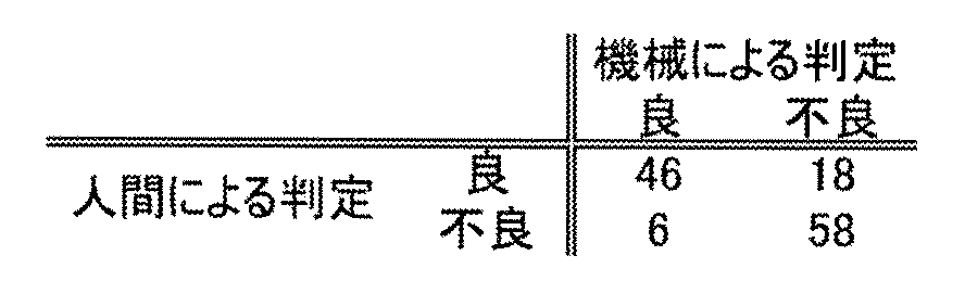
判定結果の精度は、(46+58)/128=0.81であった。
図31Aは、図30のBに示す検査画像である。図31Bは、図30のBに示す検査画像と、図30のBに示す差分画像を合成させたものである。このように2つの画像を並べることで、ユーザーに異常箇所をわかり易く提示することができる。
次に、比較として、図4及び図5Bに示すステップS25(平滑化処理)を行わずに、差分画像を取得した場合の例を図32に示す。図32に示す検査画像と生成画像は図30と同一である。
図32の差分画像をみると、どれも全体的に白の画素が多く存在し、どこに異常箇所があるか特定することが難しいことがわかる。
図30の差分画像と同様に、図32の差分画像についても、機械による良否判定を行った。判定結果を下表に示す。

判定結果の精度は、(25+38)/128=0.49であった。
以上の結果より、検査画像と生成画像の差分を取る前に、平滑化処理を行うことで、良否判定の精度が向上することが確認された。
本実施例は、本明細書で示す他の実施の形態と適宜組み合わせることができる。
10:電子顕微鏡、11:電子銃、12:集束レンズ、13:対物レンズ、14:走査コイル、15:検出器、16:ステージ、17:電子線、18:試料、19:信号電子、20:PC、21:入出力装置、30:サーバー、31:CPU、32:AIチップ、33:主記憶装置、34:補助記憶装置、35:バス、40:計算機、50:コンピュータ断層撮影装置、51:ガントリ、52:クレードル、61:開口部、62:被検体、71:X線管、72:検出器、80:画像処理装置、100:ジェネレータ、101:教師データ、101a:教師データ、101b:教師データ、101c:教師データ、102:データ、103:学習結果、103a:学習結果、103b:学習結果、103c:学習結果、110:検査画像、111:異常箇所、112:画像、113:画像、114:画像、115:画像、116:画像、117:画像、120:画像、121:領域、122:領域、130:分類器、131:画像データ、132:ラベル、133:学習結果、134:データ、200:ニューラルネットワーク、210:核磁気共鳴装置、211:ガントリ、212:クレードル、221:開口部、222:被検体、231:コイル、300:トランジスタ、311:基板、313:半導体領域、314a:低抵抗領域、314b:低抵抗領域、315:絶縁体、316:導電体、320:絶縁体、322:絶縁体、324:絶縁体、326:絶縁体、328:導電体、330:導電体、350:絶縁体、352:絶縁体、354:絶縁体、356:導電体、360:絶縁体、362:絶縁体、364:絶縁体、366:導電体、370:絶縁体、372:絶縁体、374:絶縁体、376:導電体、380:絶縁体、382:絶縁体、384:絶縁体、386:導電体、402:絶縁体、404:絶縁体、500:トランジスタ、503:導電体、503a:導電体、503b:導電体、510:絶縁体、512:絶縁体、514:絶縁体、516:絶縁体、518:導電体、520:絶縁体、522:絶縁体、524:絶縁体、530:酸化物、530a:酸化物、530b:酸化物、530c:酸化物、530c1:酸化物、530c2:酸化物、540:導電体、540a:導電体、540b:導電体、542a:導電体、542b:導電体、543a:領域、543b:領域、544:絶縁体、546:導電体、548:導電体、550:絶縁体、552:絶縁体、560:導電体、560a:導電体、560b:導電体、574:絶縁体、580:絶縁体、581:絶縁体、582:絶縁体、586:絶縁体、600:容量素子、600A:容量素子、600B:容量素子、610:導電体、611:導電体、612:導電体、620:導電体、630:絶縁体、631:絶縁体、650:絶縁体、651:絶縁体、1400:記憶装置、1411:周辺回路、1420:行回路、1430:列回路、1440:出力回路、1460:コントロールロジック回路、1470:メモリセルアレイ、1471:メモリセル、1472:メモリセル、1473:メモリセル、1474:メモリセル、1475:メモリセル、1476:メモリセル、1477:メモリセル、1478:メモリセル
Claims (16)
- 電子顕微鏡と、画像処理装置と、計算機と、を有し、
前記電子顕微鏡は、試料の表面形状に対応する信号を発生させる機能を有し、
前記画像処理装置は、前記信号に対応する第1の画像を生成する機能を有し、
前記計算機は、前記第1の画像を基にして第2の画像を取得する機能を有し、
前記計算機は、前記第1の画像に対して平滑化処理を行うことにより、第3の画像を取得する機能を有し、
前記計算機は、前記第2の画像に対して平滑化処理を行うことにより、第4の画像を取得する機能を有し、
前記計算機は、前記第3の画像と、前記第4の画像と、の差分をとることにより、第5の画像を取得する機能を有する検査装置。 - 請求項1において、
前記計算機は、ニューラルネットワークが構成された回路を有し、
前記計算機は、前記ニューラルネットワークにより、前記第1の画像を基にして前記第2の画像を取得する機能を有する検査装置。 - 請求項1又は2において、
前記第3の画像は、第1の画素値によって表され、
前記第4の画像は、第2の画素値によって表され、
前記第5の画像は、第3の画素値によって表され、
前記計算機は、前記第1の画素値と、前記第2の画素値と、の差分をとることにより、前記第3の画素値を取得する機能を有し、
前記計算機は、前記第3の画素値を基に、第4の画素値を取得する機能を有し、
前記第4の画素値は、前記第3の画素値が閾値以上である場合は、第1の値となり、
前記第4の画素値は、前記第3の画素値が前記閾値未満である場合は、第2の値となる検査装置。 - 請求項3において、
前記計算機は、前記第4の画素値によって表される第6の画像の外れ値検出を行うことにより、前記第6の画像を、異常データ又は正常データに分類する機能を有する検査装置。 - 請求項4において、
前記計算機は、入出力装置を有し、
前記計算機は、前記外れ値検出を行うことにより、前記第6の画像の異常度を算出する機能を有し、
前記計算機は、複数の前記第1の画像のそれぞれに対して、前記第6の画像を取得して、取得した前記第6の画像のそれぞれに対して前記異常度を算出する機能を有し、
前記入出力装置は、前記異常度の順に、前記第6の画像に対応する前記第1の画像を並べて表示する機能を有する検査装置。 - 請求項5において、
前記入出力装置は、前記第1の画像に前記第6の画像を合成させた第7の画像を表示する機能を有する検査装置。 - 請求項1乃至6のいずれか一項において、
前記第1の画像が、異常箇所を含む場合、前記第1の画像を基に前記計算機が取得した前記第2の画像は、前記異常箇所を含まない検査装置。 - 請求項2乃至7のいずれか一項において、
前記ニューラルネットワークが構成された回路は、チャネル形成領域に金属酸化物を用いたトランジスタを有する検査装置。 - 計算機と、電子顕微鏡と、を有する検査装置を用いた検査方法であって、
前記電子顕微鏡が撮影した第1の画像を、前記計算機が取得し、
前記計算機が、前記第1の画像を基にして第2の画像を取得し、
前記計算機が、前記第1の画像に対して平滑化処理を行うことにより第3の画像を取得し、また前記第2の画像に対して平滑化処理を行うことにより第4の画像を取得し、
前記計算機が、前記第3の画像と、前記第4の画像と、の差分をとることにより、第5の画像を取得する検査方法。 - 請求項9において、
前記計算機は、ニューラルネットワークが構成された回路を有し、
前記計算機は、前記ニューラルネットワークにより、前記第1の画像を基にして前記第2の画像を取得する検査方法。 - 請求項9又は10において、
前記計算機が、前記第3の画像を表す第1の画素値と、前記第4の画像を表す第2の画素値と、の差分を取得することにより、前記第5の画像を表す第3の画素値を取得し、
前記計算機が、前記第3の画素値が閾値以上である場合は第1の値となり、前記閾値未満である場合は第2の値となる第4の画素値を取得する検査方法。 - 請求項11において、
前記計算機が、前記第4の画素値によって表される第6の画像の外れ値検出を行うことにより、前記第6の画像を、異常データ又は正常データに分類する検査方法。 - 請求項12において、
前記計算機は、入出力装置を有し、
前記計算機が、複数の前記第1の画像のそれぞれに対して、前記第6の画像を取得して、取得した前記第6の画像の前記外れ値検出を行うことにより、前記第6の画像のそれぞれに対して異常度を算出し、
前記入出力装置が、前記異常度の順に、前記第6の画像に対応する前記第1の画像を並べて表示する検査方法。 - 請求項13において、
前記入出力装置が、前記第1の画像に前記第6の画像を合成させた第7の画像を表示する検査方法。 - 請求項9乃至14のいずれか一項において、
前記第1の画像が、異常箇所を含む場合、前記第1の画像を基に前記計算機が取得する前記第2の画像は、前記異常箇所を含まない検査方法。 - 請求項10乃至15のいずれか一項において、
前記ニューラルネットワークが構成された回路は、チャネル形成領域に金属酸化物を用いたトランジスタを有する検査方法。
Priority Applications (2)
| Application Number | Priority Date | Filing Date | Title |
|---|---|---|---|
| US17/434,033 US20220138983A1 (en) | 2019-04-02 | 2020-03-20 | Inspection device and inspection method |
| JP2021510577A JP7395566B2 (ja) | 2019-04-02 | 2020-03-20 | 検査方法 |
Applications Claiming Priority (2)
| Application Number | Priority Date | Filing Date | Title |
|---|---|---|---|
| JP2019070529 | 2019-04-02 | ||
| JP2019-070529 | 2019-04-02 |
Publications (1)
| Publication Number | Publication Date |
|---|---|
| WO2020201880A1 true WO2020201880A1 (ja) | 2020-10-08 |
Family
ID=72666585
Family Applications (1)
| Application Number | Title | Priority Date | Filing Date |
|---|---|---|---|
| PCT/IB2020/052564 Ceased WO2020201880A1 (ja) | 2019-04-02 | 2020-03-20 | 検査装置及び検査方法 |
Country Status (3)
| Country | Link |
|---|---|
| US (1) | US20220138983A1 (ja) |
| JP (1) | JP7395566B2 (ja) |
| WO (1) | WO2020201880A1 (ja) |
Families Citing this family (3)
| Publication number | Priority date | Publication date | Assignee | Title |
|---|---|---|---|---|
| WO2021152416A1 (ja) | 2020-01-31 | 2021-08-05 | 株式会社半導体エネルギー研究所 | 学習データ生成装置、不良識別システム |
| JP2024110453A (ja) * | 2023-02-03 | 2024-08-16 | 株式会社Screenホールディングス | 検査装置および検査方法 |
| KR20250109902A (ko) * | 2024-01-11 | 2025-07-18 | 삼성전자주식회사 | 스마트 스토리지 장치, 이를 포함하는 컴퓨팅 시스템, 및 그 동작 방법 |
Citations (4)
| Publication number | Priority date | Publication date | Assignee | Title |
|---|---|---|---|---|
| WO2010038859A1 (ja) * | 2008-10-03 | 2010-04-08 | 株式会社 日立ハイテクノロジーズ | パターンマッチング方法、及び画像処理装置 |
| JP2016219011A (ja) * | 2015-05-21 | 2016-12-22 | 株式会社半導体エネルギー研究所 | 電子装置 |
| WO2018173478A1 (ja) * | 2017-03-23 | 2018-09-27 | 日本電気株式会社 | 学習装置、学習方法および学習プログラム |
| WO2018211891A1 (ja) * | 2017-05-18 | 2018-11-22 | 住友電気工業株式会社 | 異変検出装置及び異変検出方法 |
Family Cites Families (8)
| Publication number | Priority date | Publication date | Assignee | Title |
|---|---|---|---|---|
| US7817844B2 (en) * | 1999-08-26 | 2010-10-19 | Nanogeometry Research Inc. | Pattern inspection apparatus and method |
| US7570797B1 (en) * | 2005-05-10 | 2009-08-04 | Kla-Tencor Technologies Corp. | Methods and systems for generating an inspection process for an inspection system |
| KR102108572B1 (ko) * | 2011-09-26 | 2020-05-07 | 가부시키가이샤 한도오따이 에네루기 켄큐쇼 | 반도체 장치 및 반도체 장치의 제작 방법 |
| JP5941782B2 (ja) * | 2012-07-27 | 2016-06-29 | 株式会社日立ハイテクノロジーズ | マッチング処理装置、マッチング処理方法、及びそれを用いた検査装置 |
| US20150103181A1 (en) * | 2013-10-16 | 2015-04-16 | Checkpoint Technologies Llc | Auto-flat field for image acquisition |
| US10402688B2 (en) * | 2016-12-07 | 2019-09-03 | Kla-Tencor Corporation | Data augmentation for convolutional neural network-based defect inspection |
| US10565702B2 (en) * | 2017-01-30 | 2020-02-18 | Dongfang Jingyuan Electron Limited | Dynamic updates for the inspection of integrated circuits |
| JP2019061577A (ja) * | 2017-09-27 | 2019-04-18 | パナソニックIpマネジメント株式会社 | 異常判定方法及びプログラム |
-
2020
- 2020-03-20 WO PCT/IB2020/052564 patent/WO2020201880A1/ja not_active Ceased
- 2020-03-20 JP JP2021510577A patent/JP7395566B2/ja active Active
- 2020-03-20 US US17/434,033 patent/US20220138983A1/en not_active Abandoned
Patent Citations (4)
| Publication number | Priority date | Publication date | Assignee | Title |
|---|---|---|---|---|
| WO2010038859A1 (ja) * | 2008-10-03 | 2010-04-08 | 株式会社 日立ハイテクノロジーズ | パターンマッチング方法、及び画像処理装置 |
| JP2016219011A (ja) * | 2015-05-21 | 2016-12-22 | 株式会社半導体エネルギー研究所 | 電子装置 |
| WO2018173478A1 (ja) * | 2017-03-23 | 2018-09-27 | 日本電気株式会社 | 学習装置、学習方法および学習プログラム |
| WO2018211891A1 (ja) * | 2017-05-18 | 2018-11-22 | 住友電気工業株式会社 | 異変検出装置及び異変検出方法 |
Also Published As
| Publication number | Publication date |
|---|---|
| JP7395566B2 (ja) | 2023-12-11 |
| US20220138983A1 (en) | 2022-05-05 |
| JPWO2020201880A1 (ja) | 2020-10-08 |
Similar Documents
| Publication | Publication Date | Title |
|---|---|---|
| US11003986B2 (en) | Semiconductor device and system using the same | |
| JP2022003826A (ja) | 撮像装置 | |
| TWI691972B (zh) | 半導體裝置、中央處理裝置及電子裝置 | |
| JP7245371B2 (ja) | 半導体装置 | |
| JP2022137140A (ja) | 電子装置、電子部品、及び、半導体パッケージ | |
| JP7217227B2 (ja) | 撮像装置、及び電子機器 | |
| JP7639207B2 (ja) | 半導体装置 | |
| US10936410B2 (en) | Memory system and information processing system | |
| KR20210134066A (ko) | 촬상 장치, 촬상 모듈, 전자 기기, 및 촬상 시스템 | |
| JP7675887B2 (ja) | Aiシステム | |
| CN113330552A (zh) | 半导体装置及包括该半导体装置的电子设备 | |
| JP7395566B2 (ja) | 検査方法 | |
| JP7661571B2 (ja) | 半導体装置および電子機器 | |
| JPWO2019048984A1 (ja) | 半導体装置、および半導体装置の作製方法 | |
| WO2021053453A1 (ja) | 半導体装置 | |
| WO2021009607A1 (ja) | 記憶装置、半導体装置、及び電子機器 | |
| US11956570B2 (en) | Imaging system and electronic device | |
| WO2021165799A1 (ja) | 半導体装置、及び電子機器 | |
| US12592714B2 (en) | Apparatus comprising analog to digital converter semiconductor device | |
| JP6690935B2 (ja) | 半導体装置 | |
| US20240143441A1 (en) | Operation method of semiconductor device | |
| US20250078895A1 (en) | Operation method of semiconductor device | |
| WO2022023866A1 (ja) | 半導体装置 | |
| KR20230071125A (ko) | 촬상 장치 및 전자 기기 | |
| JP6894726B2 (ja) | 半導体装置、および半導体装置の作製方法 |
Legal Events
| Date | Code | Title | Description |
|---|---|---|---|
| 121 | Ep: the epo has been informed by wipo that ep was designated in this application |
Ref document number: 20781913 Country of ref document: EP Kind code of ref document: A1 |
|
| ENP | Entry into the national phase |
Ref document number: 2021510577 Country of ref document: JP Kind code of ref document: A |
|
| NENP | Non-entry into the national phase |
Ref country code: DE |
|
| 122 | Ep: pct application non-entry in european phase |
Ref document number: 20781913 Country of ref document: EP Kind code of ref document: A1 |