WO2020201860A1 - 単極性トランジスタを用いて構成された論理回路、および、半導体装置 - Google Patents
単極性トランジスタを用いて構成された論理回路、および、半導体装置 Download PDFInfo
- Publication number
- WO2020201860A1 WO2020201860A1 PCT/IB2020/052186 IB2020052186W WO2020201860A1 WO 2020201860 A1 WO2020201860 A1 WO 2020201860A1 IB 2020052186 W IB2020052186 W IB 2020052186W WO 2020201860 A1 WO2020201860 A1 WO 2020201860A1
- Authority
- WO
- WIPO (PCT)
- Prior art keywords
- transistor
- drain
- source
- electrically connected
- oxide
- Prior art date
- Legal status (The legal status is an assumption and is not a legal conclusion. Google has not performed a legal analysis and makes no representation as to the accuracy of the status listed.)
- Ceased
Links
Images

















Classifications
-
- H—ELECTRICITY
- H03—ELECTRONIC CIRCUITRY
- H03K—PULSE TECHNIQUE
- H03K19/00—Logic circuits, i.e. having at least two inputs acting on one output; Inverting circuits
- H03K19/02—Logic circuits, i.e. having at least two inputs acting on one output; Inverting circuits using specified components
- H03K19/08—Logic circuits, i.e. having at least two inputs acting on one output; Inverting circuits using specified components using semiconductor devices
-
- H—ELECTRICITY
- H03—ELECTRONIC CIRCUITRY
- H03K—PULSE TECHNIQUE
- H03K17/00—Electronic switching or gating, i.e. not by contact-making and –breaking
- H03K17/06—Modifications for ensuring a fully conducting state
- H03K17/063—Modifications for ensuring a fully conducting state in field-effect transistor switches
-
- H—ELECTRICITY
- H03—ELECTRONIC CIRCUITRY
- H03K—PULSE TECHNIQUE
- H03K17/00—Electronic switching or gating, i.e. not by contact-making and –breaking
- H03K17/51—Electronic switching or gating, i.e. not by contact-making and –breaking characterised by the components used
- H03K17/56—Electronic switching or gating, i.e. not by contact-making and –breaking characterised by the components used by the use, as active elements, of semiconductor devices
-
- H—ELECTRICITY
- H03—ELECTRONIC CIRCUITRY
- H03K—PULSE TECHNIQUE
- H03K19/00—Logic circuits, i.e. having at least two inputs acting on one output; Inverting circuits
- H03K19/0175—Coupling arrangements; Interface arrangements
- H03K19/0185—Coupling arrangements; Interface arrangements using field effect transistors only
-
- H—ELECTRICITY
- H03—ELECTRONIC CIRCUITRY
- H03K—PULSE TECHNIQUE
- H03K19/00—Logic circuits, i.e. having at least two inputs acting on one output; Inverting circuits
- H03K19/02—Logic circuits, i.e. having at least two inputs acting on one output; Inverting circuits using specified components
- H03K19/08—Logic circuits, i.e. having at least two inputs acting on one output; Inverting circuits using specified components using semiconductor devices
- H03K19/094—Logic circuits, i.e. having at least two inputs acting on one output; Inverting circuits using specified components using semiconductor devices using field-effect transistors
-
- H—ELECTRICITY
- H03—ELECTRONIC CIRCUITRY
- H03K—PULSE TECHNIQUE
- H03K19/00—Logic circuits, i.e. having at least two inputs acting on one output; Inverting circuits
- H03K19/02—Logic circuits, i.e. having at least two inputs acting on one output; Inverting circuits using specified components
- H03K19/08—Logic circuits, i.e. having at least two inputs acting on one output; Inverting circuits using specified components using semiconductor devices
- H03K19/094—Logic circuits, i.e. having at least two inputs acting on one output; Inverting circuits using specified components using semiconductor devices using field-effect transistors
- H03K19/0944—Logic circuits, i.e. having at least two inputs acting on one output; Inverting circuits using specified components using semiconductor devices using field-effect transistors using MOSFET or insulated gate field-effect transistors, i.e. IGFET
-
- H—ELECTRICITY
- H10—SEMICONDUCTOR DEVICES; ELECTRIC SOLID-STATE DEVICES NOT OTHERWISE PROVIDED FOR
- H10D—INORGANIC ELECTRIC SEMICONDUCTOR DEVICES
- H10D84/00—Integrated devices formed in or on semiconductor substrates that comprise only semiconducting layers, e.g. on Si wafers or on GaAs-on-Si wafers
-
- H—ELECTRICITY
- H10—SEMICONDUCTOR DEVICES; ELECTRIC SOLID-STATE DEVICES NOT OTHERWISE PROVIDED FOR
- H10D—INORGANIC ELECTRIC SEMICONDUCTOR DEVICES
- H10D84/00—Integrated devices formed in or on semiconductor substrates that comprise only semiconducting layers, e.g. on Si wafers or on GaAs-on-Si wafers
- H10D84/01—Manufacture or treatment
- H10D84/0123—Integrating together multiple components covered by H10D12/00 or H10D30/00, e.g. integrating multiple IGBTs
- H10D84/0126—Integrating together multiple components covered by H10D12/00 or H10D30/00, e.g. integrating multiple IGBTs the components including insulated gates, e.g. IGFETs
-
- H—ELECTRICITY
- H10—SEMICONDUCTOR DEVICES; ELECTRIC SOLID-STATE DEVICES NOT OTHERWISE PROVIDED FOR
- H10D—INORGANIC ELECTRIC SEMICONDUCTOR DEVICES
- H10D84/00—Integrated devices formed in or on semiconductor substrates that comprise only semiconducting layers, e.g. on Si wafers or on GaAs-on-Si wafers
- H10D84/01—Manufacture or treatment
- H10D84/02—Manufacture or treatment characterised by using material-based technologies
- H10D84/03—Manufacture or treatment characterised by using material-based technologies using Group IV technology, e.g. silicon technology or silicon-carbide [SiC] technology
- H10D84/038—Manufacture or treatment characterised by using material-based technologies using Group IV technology, e.g. silicon technology or silicon-carbide [SiC] technology using silicon technology, e.g. SiGe
-
- H—ELECTRICITY
- H03—ELECTRONIC CIRCUITRY
- H03K—PULSE TECHNIQUE
- H03K17/00—Electronic switching or gating, i.e. not by contact-making and –breaking
- H03K17/06—Modifications for ensuring a fully conducting state
- H03K2017/066—Maximizing the OFF-resistance instead of minimizing the ON-resistance
-
- H—ELECTRICITY
- H03—ELECTRONIC CIRCUITRY
- H03K—PULSE TECHNIQUE
- H03K2217/00—Indexing scheme related to electronic switching or gating, i.e. not by contact-making or -breaking covered by H03K17/00
- H03K2217/0036—Means reducing energy consumption
-
- H—ELECTRICITY
- H10—SEMICONDUCTOR DEVICES; ELECTRIC SOLID-STATE DEVICES NOT OTHERWISE PROVIDED FOR
- H10D—INORGANIC ELECTRIC SEMICONDUCTOR DEVICES
- H10D30/00—Field-effect transistors [FET]
- H10D30/60—Insulated-gate field-effect transistors [IGFET]
- H10D30/67—Thin-film transistors [TFT]
- H10D30/6729—Thin-film transistors [TFT] characterised by the electrodes
- H10D30/673—Thin-film transistors [TFT] characterised by the electrodes characterised by the shapes, relative sizes or dispositions of the gate electrodes
- H10D30/6733—Multi-gate TFTs
- H10D30/6734—Multi-gate TFTs having gate electrodes arranged on both top and bottom sides of the channel, e.g. dual-gate TFTs
-
- H—ELECTRICITY
- H10—SEMICONDUCTOR DEVICES; ELECTRIC SOLID-STATE DEVICES NOT OTHERWISE PROVIDED FOR
- H10D—INORGANIC ELECTRIC SEMICONDUCTOR DEVICES
- H10D30/00—Field-effect transistors [FET]
- H10D30/60—Insulated-gate field-effect transistors [IGFET]
- H10D30/67—Thin-film transistors [TFT]
- H10D30/674—Thin-film transistors [TFT] characterised by the active materials
- H10D30/6755—Oxide semiconductors, e.g. zinc oxide, copper aluminium oxide or cadmium stannate
-
- H—ELECTRICITY
- H10—SEMICONDUCTOR DEVICES; ELECTRIC SOLID-STATE DEVICES NOT OTHERWISE PROVIDED FOR
- H10D—INORGANIC ELECTRIC SEMICONDUCTOR DEVICES
- H10D30/00—Field-effect transistors [FET]
- H10D30/60—Insulated-gate field-effect transistors [IGFET]
- H10D30/67—Thin-film transistors [TFT]
- H10D30/6757—Thin-film transistors [TFT] characterised by the structure of the channel, e.g. transverse or longitudinal shape or doping profile
-
- H—ELECTRICITY
- H10—SEMICONDUCTOR DEVICES; ELECTRIC SOLID-STATE DEVICES NOT OTHERWISE PROVIDED FOR
- H10D—INORGANIC ELECTRIC SEMICONDUCTOR DEVICES
- H10D30/00—Field-effect transistors [FET]
- H10D30/60—Insulated-gate field-effect transistors [IGFET]
- H10D30/791—Arrangements for exerting mechanical stress on the crystal lattice of the channel regions
- H10D30/797—Arrangements for exerting mechanical stress on the crystal lattice of the channel regions being in source or drain regions, e.g. SiGe source or drain
-
- H—ELECTRICITY
- H10—SEMICONDUCTOR DEVICES; ELECTRIC SOLID-STATE DEVICES NOT OTHERWISE PROVIDED FOR
- H10D—INORGANIC ELECTRIC SEMICONDUCTOR DEVICES
- H10D86/00—Integrated devices formed in or on insulating or conducting substrates, e.g. formed in silicon-on-insulator [SOI] substrates or on stainless steel or glass substrates
- H10D86/80—Integrated devices formed in or on insulating or conducting substrates, e.g. formed in silicon-on-insulator [SOI] substrates or on stainless steel or glass substrates characterised by multiple passive components, e.g. resistors, capacitors or inductors
-
- H—ELECTRICITY
- H10—SEMICONDUCTOR DEVICES; ELECTRIC SOLID-STATE DEVICES NOT OTHERWISE PROVIDED FOR
- H10D—INORGANIC ELECTRIC SEMICONDUCTOR DEVICES
- H10D87/00—Integrated devices comprising both bulk components and either SOI or SOS components on the same substrate
Definitions
- One embodiment of the present invention relates to a logic circuit configured by using a unipolar transistor.
- the semiconductor device refers to all devices that can function by utilizing semiconductor characteristics.
- an integrated circuit, a chip having an integrated circuit, an electronic component in which the chip is housed in a package, and an electronic device having an integrated circuit are examples of semiconductor devices.
- One form of the present invention is not limited to the above technical fields.
- the technical field of the invention disclosed in the present specification and the like relates to a product, a method, or a manufacturing method.
- one embodiment of the present invention relates to a process, machine, manufacture, or composition (composition of matter).
- CMOS also referred to as a digital circuit or logic circuit
- a circuit also referred to as a digital circuit or logic circuit
- Complementary Metal Oxide Digital Circuit circuits are widely used.
- CMOS circuits are supplied with high and low power potentials, high levels are represented using high power potentials and low levels are represented using low power potentials.
- the CMOS circuit is configured by using, for example, an n-channel transistor and a p-channel transistor formed on a single crystal silicon substrate.
- the CMOS circuit has a circuit configuration in which an n-channel transistor and a p-channel transistor are connected in series between a high power potential and a low power potential, and when the n-channel transistor is in a conductive state, the p-channel transistor is When the n-channel transistor is in the non-conducting state and the n-channel transistor is in the non-conducting state, the p-channel transistor is in the non-conducting state. That is, after the high level or the low level is determined, the through current does not flow from the high power supply potential to the low power supply potential (excluding the off current of the transistor).
- a logic circuit may be configured by using a unipolar transistor or a unichannel transistor).
- Patent Document 1 and Patent Document 2 disclose examples of a drive circuit of a semiconductor device or a display device configured by using a unipolar transistor.
- two unipolar transistors are connected in series between the high power supply potential and the low power supply potential, and the logic (high level or low level) of the first signal and the first signal is inverted.
- the second signal is input to the gate of each transistor, and has a circuit configuration in which a through current does not flow from a high power supply potential to a low power supply potential.
- the method of using the first signal and the second signal in which the logic of the first signal is inverted may be called dual rail.
- Patent Document 1 and Patent Document 2 the problem that one of the high level and the low level of the output signal does not reach the high power supply potential or the low power supply potential is caused by the capacitance between the output terminal and the gate of one transistor. It is solved by providing.
- the method of providing a capacitance between the output terminal and the gate of one of the transistors is sometimes called a bootstrap.
- transistors having metal oxides in the channel formation region have been attracting attention in recent years.
- an OS transistor an n-channel transistor has been put into practical use. It is a thin film transistor that has a very small off-current, can apply a high voltage between the source and drain (also called a high withstand voltage), and is laminated. It has features such as being able to be provided. Further, the OS transistor has a feature that the off-current does not easily increase even in a high-temperature environment and the ratio of the on-current to the off-current is large even in a high-temperature environment, and the semiconductor device configured by using the OS transistor is reliable. Is high.
- Patent Document 3 describes a semiconductor device having a plurality of memory cells using OS transistors on a semiconductor substrate on which peripheral circuits such as a drive circuit and a control circuit are formed, and a memory of a DRAM (Dynamic Random Access Memory).
- an OS transistor is used in a cell.
- a peripheral circuit can be configured by using a Si transistor formed on a single crystal silicon substrate, and a memory cell using an OS transistor can be laminated and provided above the peripheral circuit.
- the chip area can be reduced.
- the off current of the OS transistor is very small, the stored data can be retained for a long time.
- JP-A-9-246936 Japanese Unexamined Patent Publication No. 2002-328634 Japanese Unexamined Patent Publication No. 2012-256820
- Patent Document 1 and Patent Document 2 dual rails and boot straps are adopted, and although it is a logic circuit configured by using a unipolar transistor, it is high after a high level or a low level is determined as in a CMOS circuit. It has a feature that a through current does not flow from a power supply potential to a low power supply potential (also called a steady current does not flow), and a high power supply potential can be used to represent a high level and a low power supply potential can be used to represent a low level. , The circuit is disclosed.
- the voltage Vgs of the gate with respect to the source of the transistor is sufficiently secured in the transistor in which the capacitance is provided between the source and the gate. If the gate voltage Vgs with respect to the source of the transistor is not sufficiently secured, the high level may not rise to the high power supply potential, or the low level may not fall to the low power supply potential.
- the source of the transistor is electrically connected to the output terminal, and a capacitance is provided between the source of the transistor and the gate.
- a capacitive load is connected to the output terminal, the potential of the output terminal may not rise to the high power potential at high level, or may not fall to the low power potential at low level. It was.
- One embodiment of the present invention is a logic circuit configured by using a unipolar transistor, and when a steady current does not flow and the output is high level, the potential of the output terminal rises to a high power supply potential and the output is low level. At this time, one of the problems is to provide a logic circuit in which the potential of the output terminal is lowered to the low power supply potential.
- one embodiment of the present invention is a semiconductor device configured by using a unipolar transistor, and when a steady current does not flow and the output is at a high level, the potential of the output terminal rises to a high power supply potential and the output becomes high.
- One of the problems is to provide a semiconductor device in which the potential of the output terminal drops to a low power supply potential at a low level.
- one embodiment of the present invention does not necessarily have to solve all of the above problems, but may solve at least one problem. Moreover, the description of the above-mentioned problem does not prevent the existence of other problem. Issues other than these are self-evident from the description of the description, claims, drawings, etc., and it is possible to extract issues other than these from the description of the specification, claims, drawings, etc. It is possible.
- the first to eighth transistors, the first and second capacitive elements, the first and second wirings, the first and second input terminals, and the first and second output terminals are provided. It is a semiconductor device that has. One of the source or drain of the first transistor is electrically connected to the first wiring, and the other of the source or drain of the first transistor is one of the source or drain of the second transistor, one terminal of the first capacitance element. , And the other of the source or drain of the second transistor is electrically connected to the second wiring.
- the gate of the first transistor includes the gate of the fourth transistor, one of the source or drain of the eighth transistor, one of the source or drain of the seventh transistor, one terminal of the second capacitive element, and the gate of the sixth transistor.
- the gate of the second transistor is the other terminal of the first capacitive element, one of the source or drain of the fourth transistor, one of the source or drain of the third transistor, the gate of the eighth transistor, and It is electrically connected to the gate of the fifth transistor.
- the other of the source or drain of the fourth transistor is electrically connected to the first wiring
- the other of the source or drain of the third transistor is electrically connected to the second wiring
- the gate of the third transistor is the third.
- Electrically connected to the 2 input terminal, the other of the source or drain of the 8th transistor is electrically connected to the 1st wiring, and the other of the source or drain of the 7th transistor is electrically connected to the 2nd wiring.
- the gate of the 7th transistor is electrically connected to the 1st input terminal.
- One of the source or drain of the fifth transistor is electrically connected to the first wiring, and the other of the source or drain of the fifth transistor is one of the source or drain of the sixth transistor, the other terminal of the second capacitive element.
- the second output terminal is electrically connected, and the other of the source or drain of the sixth transistor is electrically connected to the second wiring.
- the first to eighth transistors are n-channel type.
- the first to eighth transistors have a metal oxide in the channel forming region.
- one embodiment of the present invention includes first to sixth transistors, first and second capacitive elements, first and second wirings, first and second input terminals, and first and second output terminals. It is a semiconductor device having and. One of the source or drain of the first transistor is electrically connected to the first wiring, and the other of the source or drain of the first transistor is one of the source or drain of the second transistor, the gate of the fourth transistor, the first. It is electrically connected to one terminal of the capacitive element and the first output terminal, and the other of the source or drain of the second transistor is electrically connected to the second wiring.
- the gate of the first transistor is electrically connected to one of the source or drain of the fourth transistor, one of the source or drain of the fifth transistor, one terminal of the second capacitive element, and the second output terminal.
- the gate of the two transistors is electrically connected to one of the source or drain of the third transistor and the other terminal of the first capacitive element, and the gate of the third transistor is electrically connected to the second wiring.
- the other of the source or drain of the third transistor is electrically connected to the second input terminal.
- the other of the source or drain of the fourth transistor is electrically connected to the first wiring
- the other of the source or drain of the fifth transistor is electrically connected to the second wiring
- the gate of the fifth transistor is the third.
- the gate of the 6th transistor is electrically connected to the 2nd wiring and the source or drain of the 6th transistor.
- the other is electrically connected to the first input terminal.
- the first to sixth transistors are n-channel type.
- the first to sixth transistors have a metal oxide in the channel forming region.
- one embodiment of the present invention includes first to tenth transistors, first and second capacitive elements, first and second wirings, first to fourth input terminals, and first and second output terminals. It is a semiconductor device having and. One of the source or drain of the first transistor is electrically connected to the first wiring, and the other of the source or drain of the first transistor is one of the source or drain of the second transistor, one terminal of the first capacitance element. , And the other of the source or drain of the second transistor is electrically connected to the second wiring.
- the gate of the first transistor includes the gate of the fifth transistor, one of the source or drain of the tenth transistor, one of the source or drain of the ninth transistor, one terminal of the second capacitance element, and the gate of the seventh transistor.
- the gate of the second transistor is the other terminal of the first capacitive element, one of the source or drain of the fourth transistor, one of the source or drain of the third transistor, the source or drain of the fifth transistor.
- it is electrically connected to the gate of the 10th transistor and the gate of the 6th transistor.
- the other of the source or drain of the fifth transistor is electrically connected to the first wiring, and the other of the source or drain of the fourth transistor is electrically connected to the second wiring of the source or drain of the third transistor.
- the other is electrically connected to the second wiring, the gate of the fourth transistor is electrically connected to the fourth input terminal, and the gate of the third transistor is electrically connected to the second input terminal.
- the other of the source or drain of the tenth transistor is electrically connected to the first wiring
- the other of the source or drain of the ninth transistor is electrically connected to one of the source or drain of the eighth transistor
- the eighth The other of the transistor source or drain is electrically connected to the second wiring
- the gate of the ninth transistor is electrically connected to the third input terminal
- the gate of the eighth transistor is electrically connected to the first input terminal.
- One of the source or drain of the sixth transistor is electrically connected to the first wiring
- the other of the source or drain of the sixth transistor is one of the source or drain of the seventh transistor, the other terminal of the second capacitive element.
- the second output terminal is electrically connected, and the other of the source or drain of the seventh transistor is electrically connected to the second wiring.
- the first to tenth transistors are n-channel type.
- the first to tenth transistors have a metal oxide in the channel forming region.
- one embodiment of the present invention includes first to tenth transistors, first and second capacitive elements, first and second wirings, first to fourth input terminals, and first and second output terminals. It is a semiconductor device having and. One of the source or drain of the first transistor is electrically connected to the first wiring, and the other of the source or drain of the first transistor is one of the source or drain of the second transistor, one terminal of the first capacitance element. , And the other of the source or drain of the second transistor is electrically connected to the second wiring.
- the gate of the first transistor is the gate of the fifth transistor, one of the source or drain of the tenth transistor, one of the source or drain of the eighth transistor, one of the source or drain of the ninth transistor, and one of the second capacitive elements.
- the gate of the 2nd transistor is the other terminal of the 1st capacitive element, one of the source or drain of the 4th transistor, and the source or drain of the 5th transistor.
- it is electrically connected to the gate of the 10th transistor and the gate of the 6th transistor.
- the other of the source or drain of the fifth transistor is electrically connected to the first wiring
- the other of the source or drain of the fourth transistor is electrically connected to one of the source or drain of the third transistor
- the third The other of the transistor source or drain is electrically connected to the second wiring
- the gate of the fourth transistor is electrically connected to the fourth input terminal
- the gate of the third transistor is electrically connected to the second input terminal.
- the other of the source or drain of the tenth transistor is electrically connected to the first wiring
- the other of the source or drain of the eighth transistor is electrically connected to the second wiring of the source or drain of the ninth transistor.
- the other is electrically connected to the second wiring
- the gate of the eighth transistor is electrically connected to the first input terminal
- the gate of the ninth transistor is electrically connected to the third input terminal.
- One of the source or drain of the sixth transistor is electrically connected to the first wiring
- the other of the source or drain of the sixth transistor is one of the source or drain of the seventh transistor, the other terminal of the second capacitive element.
- the second output terminal is electrically connected, and the other of the source or drain of the seventh transistor is electrically connected to the second wiring.
- the first to tenth transistors are n-channel type.
- the first to tenth transistors have a metal oxide in the channel forming region.
- the first to eighth transistors, the first and second capacitive elements, the first and second wirings, the first and second input terminals, and the first and second output terminals are provided. It is a semiconductor device that has. One of the source or drain of the first transistor is electrically connected to the first wiring, and the other of the source or drain of the first transistor is one of the source or drain of the second transistor, one terminal of the first capacitance element. , And the other of the source or drain of the second transistor is electrically connected to the second wiring.
- the gate of the first transistor includes the gate of the fourth transistor, one of the source or drain of the eighth transistor, one of the source or drain of the seventh transistor, one terminal of the second capacitive element, and the gate of the sixth transistor.
- the gate of the second transistor is the other terminal of the first capacitive element, one of the source or drain of the fourth transistor, one of the source or drain of the third transistor, the gate of the eighth transistor, and It is electrically connected to the gate of the fifth transistor.
- the other of the source or drain of the fourth transistor is electrically connected to the first wiring
- the other of the source or drain of the third transistor is electrically connected to the second wiring
- the gate of the third transistor is the third.
- Electrically connected to the 2 input terminal, the other of the source or drain of the 8th transistor is electrically connected to the 1st wiring, and the other of the source or drain of the 7th transistor is electrically connected to the 2nd wiring.
- the gate of the 7th transistor is electrically connected to the 1st input terminal.
- One of the source or drain of the fifth transistor is electrically connected to the first wiring, and the other of the source or drain of the fifth transistor is one of the source or drain of the sixth transistor, the other terminal of the second capacitive element.
- the second output terminal is electrically connected, and the other of the source or drain of the sixth transistor is electrically connected to the second wiring.
- the first potential is supplied to the first wiring
- the second potential is supplied to the second wiring
- the second potential is a potential higher than the first potential
- the first signal is input to the first input terminal.
- the second signal is input to the second input terminal, and the second signal is a signal in which the logic of the first signal is inverted.
- the first to eighth transistors are n-channel type.
- the first to eighth transistors have a metal oxide in the channel forming region.
- one embodiment of the present invention includes first to sixth transistors, first and second capacitive elements, first and second wirings, first and second input terminals, and first and second output terminals. It is a semiconductor device having and. One of the source or drain of the first transistor is electrically connected to the first wiring, and the other of the source or drain of the first transistor is one of the source or drain of the second transistor, the gate of the fourth transistor, the first. It is electrically connected to one terminal of the capacitive element and the first output terminal, and the other of the source or drain of the second transistor is electrically connected to the second wiring.
- the gate of the first transistor is electrically connected to one of the source or drain of the fourth transistor, one of the source or drain of the fifth transistor, one terminal of the second capacitive element, and the second output terminal.
- the gate of the two transistors is electrically connected to one of the source or drain of the third transistor and the other terminal of the first capacitive element, and the gate of the third transistor is electrically connected to the second wiring.
- the other of the source or drain of the third transistor is electrically connected to the second input terminal.
- the other of the source or drain of the fourth transistor is electrically connected to the first wiring
- the other of the source or drain of the fifth transistor is electrically connected to the second wiring
- the gate of the fifth transistor is the third.
- the gate of the 6th transistor is electrically connected to the 2nd wiring and the source or drain of the 6th transistor.
- the other is electrically connected to the first input terminal.
- the first potential is supplied to the first wiring
- the second potential is supplied to the second wiring
- the second potential is a potential higher than the first potential
- the first signal is input to the first input terminal.
- the second signal is input to the second input terminal, and the second signal is a signal in which the logic of the first signal is inverted.
- the first to sixth transistors are n-channel type.
- the first to sixth transistors have a metal oxide in the channel forming region.
- one embodiment of the present invention includes first to tenth transistors, first and second capacitive elements, first and second wirings, first to fourth input terminals, and first and second output terminals. It is a semiconductor device having and. One of the source or drain of the first transistor is electrically connected to the first wiring, and the other of the source or drain of the first transistor is one of the source or drain of the second transistor, one terminal of the first capacitance element. , And the other of the source or drain of the second transistor is electrically connected to the second wiring.
- the gate of the first transistor includes the gate of the fifth transistor, one of the source or drain of the tenth transistor, one of the source or drain of the ninth transistor, one terminal of the second capacitance element, and the gate of the seventh transistor.
- the gate of the second transistor is the other terminal of the first capacitive element, one of the source or drain of the fourth transistor, one of the source or drain of the third transistor, the source or drain of the fifth transistor.
- it is electrically connected to the gate of the 10th transistor and the gate of the 6th transistor.
- the other of the source or drain of the fifth transistor is electrically connected to the first wiring, and the other of the source or drain of the fourth transistor is electrically connected to the second wiring of the source or drain of the third transistor.
- the other is electrically connected to the second wiring, the gate of the fourth transistor is electrically connected to the fourth input terminal, and the gate of the third transistor is electrically connected to the second input terminal.
- the other of the source or drain of the tenth transistor is electrically connected to the first wiring
- the other of the source or drain of the ninth transistor is electrically connected to one of the source or drain of the eighth transistor
- the eighth The other of the transistor source or drain is electrically connected to the second wiring
- the gate of the ninth transistor is electrically connected to the third input terminal
- the gate of the eighth transistor is electrically connected to the first input terminal.
- One of the source or drain of the sixth transistor is electrically connected to the first wiring
- the other of the source or drain of the sixth transistor is one of the source or drain of the seventh transistor, the other terminal of the second capacitive element.
- the second output terminal is electrically connected, and the other of the source or drain of the seventh transistor is electrically connected to the second wiring.
- a first potential is supplied to the first wiring
- a second potential is supplied to the second wiring
- the second potential is a potential higher than the first potential
- the first signal is input to the first input terminal.
- the second signal is input to the second input terminal
- the third signal is input to the third input terminal
- the fourth signal is input to the fourth input terminal
- the second signal is the logic of the first signal. Is an inverted signal
- the fourth signal is a signal in which the logic of the third signal is inverted.
- the first to tenth transistors are n-channel type.
- the first to tenth transistors have a metal oxide in the channel forming region.
- one embodiment of the present invention includes first to tenth transistors, first and second capacitive elements, first and second wirings, first to fourth input terminals, and first and second output terminals. It is a semiconductor device having and. One of the source or drain of the first transistor is electrically connected to the first wiring, and the other of the source or drain of the first transistor is one of the source or drain of the second transistor, one terminal of the first capacitance element. , And the other of the source or drain of the second transistor is electrically connected to the second wiring.
- the gate of the first transistor is the gate of the fifth transistor, one of the source or drain of the tenth transistor, one of the source or drain of the eighth transistor, one of the source or drain of the ninth transistor, and one of the second capacitive elements.
- the gate of the 2nd transistor is the other terminal of the 1st capacitive element, one of the source or drain of the 4th transistor, and the source or drain of the 5th transistor.
- it is electrically connected to the gate of the 10th transistor and the gate of the 6th transistor.
- the other of the source or drain of the fifth transistor is electrically connected to the first wiring
- the other of the source or drain of the fourth transistor is electrically connected to one of the source or drain of the third transistor
- the third The other of the transistor source or drain is electrically connected to the second wiring
- the gate of the fourth transistor is electrically connected to the fourth input terminal
- the gate of the third transistor is electrically connected to the second input terminal.
- the other of the source or drain of the tenth transistor is electrically connected to the first wiring
- the other of the source or drain of the eighth transistor is electrically connected to the second wiring of the source or drain of the ninth transistor.
- the other is electrically connected to the second wiring
- the gate of the eighth transistor is electrically connected to the first input terminal
- the gate of the ninth transistor is electrically connected to the third input terminal.
- One of the source or drain of the sixth transistor is electrically connected to the first wiring
- the other of the source or drain of the sixth transistor is one of the source or drain of the seventh transistor, the other terminal of the second capacitive element.
- the second output terminal is electrically connected, and the other of the source or drain of the seventh transistor is electrically connected to the second wiring.
- a first potential is supplied to the first wiring
- a second potential is supplied to the second wiring
- the second potential is a potential higher than the first potential
- the first signal is input to the first input terminal.
- the second signal is input to the second input terminal
- the third signal is input to the third input terminal
- the fourth signal is input to the fourth input terminal
- the second signal is the logic of the first signal. Is an inverted signal
- the fourth signal is a signal in which the logic of the third signal is inverted.
- the first to tenth transistors are n-channel type.
- the first to tenth transistors have a metal oxide in the channel forming region.
- the logic circuit is configured by using a unipolar transistor, when the steady current does not flow and the output is high level, the potential of the output terminal rises to the high power supply potential and the output is low level. At this time, it is possible to provide a logic circuit in which the potential of the output terminal drops to a low power supply potential.
- the semiconductor device is configured by using a unipolar transistor, when the steady current does not flow and the output is at a high level, the potential of the output terminal rises to a high power supply potential and the output becomes high. It is possible to provide a semiconductor device in which the potential of the output terminal drops to a low power supply potential at a low level.
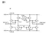
- FIG. 1 is a circuit diagram showing a configuration example of a semiconductor device.
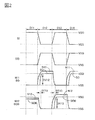
- FIG. 2 is a timing chart.
- FIG. 3 is a circuit diagram showing a configuration example of a semiconductor device.
- FIG. 4 is a timing chart.
- 5A and 5B are diagrams showing circuit diagram symbols of transistors.
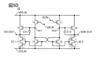
- 5C and 5D are circuit diagrams showing a configuration example of a semiconductor device.
- FIG. 6 is a circuit diagram showing a configuration example of a semiconductor device.
- FIG. 7 is a circuit diagram showing a configuration example of a semiconductor device.
- FIG. 8 is a timing chart.
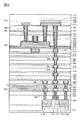
- FIG. 9 is a cross-sectional view showing a configuration example of the semiconductor device.
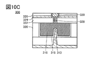
- 10A, 10B, and 10C are cross-sectional views showing a structural example of the transistor.
- FIG. 11A is a top view showing a structural example of the transistor.
- 11B and 11C are cross-sectional views showing a structural example of the transistor.
- FIG. 12A is a top view showing a structural example of the transistor.
- 12B and 12C are cross-sectional views showing a structural example of the transistor.
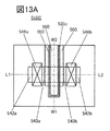
- FIG. 13A is a top view showing a structural example of the transistor.
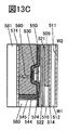
- 13B and 13C are cross-sectional views showing a structural example of the transistor.
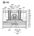
- FIG. 14A is a top view showing a structural example of the transistor.
- 14B and 14C are cross-sectional views showing a structural example of the transistor.
- FIG. 15A is a top view showing a structural example of the transistor.
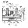
- 15B and 15C are cross-sectional views showing a structural example of the transistor.
- FIG. 15A is a top view showing a structural example of the transistor.
- 15B and 15C are cross-sectional views showing a structural example of the transistor.
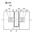
- 16A is a top view showing a structural example of the transistor.
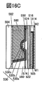
- 16B and 16C are cross-sectional views showing a structural example of the transistor.
- 17A and 17B are cross-sectional views showing a structural example of the transistor.
- FIG. 18 is a cross-sectional view showing a configuration example of the semiconductor device.
- 19A and 19B are cross-sectional views showing a structural example of the transistor.
- FIG. 20A is a diagram illustrating classification of the crystal structure of IGZO.
- FIG. 20B is a diagram illustrating an XRD spectrum of quartz glass.
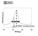
- FIG. 20C is a diagram illustrating an XRD spectrum of crystalline IGZO.
- FIG. 20D is a diagram illustrating a microelectron diffraction pattern of crystalline IGZO.
- membrane and the term “layer” can be interchanged with each other.
- conductive layer to the term “conductive layer”.
- insulating film to the term “insulating layer”.
- gate electrode on the gate insulating layer does not exclude those containing other components between the gate insulating layer and the gate electrode.
- the code when the same code is used for a plurality of elements, and when it is particularly necessary to distinguish them, the code may be "_1", “_2", “[n]", “[m,”. It may be described with an identification code such as "n]".
- the second wiring GL is described as wiring GL [2].
- “electrically connected” includes a case where they are connected via "something having some kind of electrical action".
- the "thing having some kind of electrical action” is not particularly limited as long as it enables the exchange of electric signals between the connection targets.
- “things having some kind of electrical action” include electrodes, wirings, switching elements such as transistors, resistance elements, inductors, capacitive elements, and other elements having various functions. Further, even when it is expressed as “electrically connected”, there is a case where there is no physical connection part in the actual circuit and only the wiring is extended.
- Electrode and “wiring” do not functionally limit these components.
- an “electrode” may be used as part of a “wiring” and vice versa.
- the "terminal" in the electric circuit means a portion where current or potential input (or output) and signal reception (or transmission) are performed. Therefore, a part of the wiring or the electrode may function as a terminal.
- the “capacity” has a configuration in which two electrodes face each other via an insulator (dielectric).
- the “capacitive element” includes the above-mentioned “capacity”. That is, in the present specification and the like, the “capacitive element” has a structure in which two electrodes face each other via an insulator, a structure in which two wires face each other via an insulator, or a structure in which two wires face each other through an insulator. This includes the case where the two wires are arranged via an insulator.
- the “voltage” often indicates a potential difference between a certain potential and a reference potential (for example, a ground potential). Therefore, the voltage and the potential difference can be rephrased.
- a transistor is an element having at least three terminals including a gate, a drain, and a source. Then, a channel forming region is provided between the drain (drain terminal, drain region, or drain electrode) and the source (source terminal, source region, or source electrode), and the source and drain are passed through the channel forming region. It is possible to pass a current between and.
- the channel forming region means a region in which a current mainly flows.
- the functions of the source and the drain may be interchanged when transistors having different polarities are adopted or when the direction of the current changes in the circuit operation. Therefore, in the present specification and the like, the terms source and drain can be used interchangeably.
- the off current means a drain current when the transistor is in an off state (also referred to as a non-conducting state or a cutoff state).
- the off state means that the gate voltage Vgs with respect to the source is lower than the threshold voltage Vth in the n-channel transistor, and the gate voltage Vgs with respect to the source is the threshold voltage in the p-channel transistor.
- drain may be read as source. That is, the off current may refer to the source current when the transistor is in the off state. In addition, it may be called a leak current in the same meaning as an off current. Further, in the present specification and the like, the off current may refer to the current flowing between the source and the drain when the transistor is in the off state.
- the on-current may refer to the current flowing between the source and the drain when the transistor is in the on state (also referred to as the conduction state).
- a metal oxide is a metal oxide in a broad sense. Metal oxides are classified into oxide insulators, oxide conductors (including transparent oxide conductors), oxide semiconductors, and the like.
- the metal oxide when a metal oxide is used in the channel forming region of a transistor, the metal oxide may be referred to as an oxide semiconductor. That is, when a metal oxide has at least one of an amplification action, a rectifying action, and a switching action, the metal oxide can be referred to as a metal oxide semiconductor (metal oxide semiconductor). That is, a transistor having a metal oxide in the channel forming region can be called an "oxide semiconductor transistor" or an "OS transistor". Similarly, the above-mentioned "transistor using an oxide semiconductor” is also a transistor having a metal oxide in the channel forming region.
- a metal oxide having nitrogen may also be referred to as a metal oxide. Further, a metal oxide having nitrogen may be referred to as a metal oxynitride. Details of the metal oxide will be described later.
- the semiconductor device according to one embodiment of the present invention is a logic circuit configured by using a unipolar transistor, in which a high power supply potential is used to represent a high level, and a low power supply potential is used to represent a low level.
- n-channel type transistor is used for the semiconductor device described in the present specification and the like
- p-channel type transistor can also be used.
- the change from the n-channel transistor to the p-channel transistor is easily understood by those skilled in the art, and the description thereof will be omitted.
- FIG. 1 is a circuit diagram showing a configuration example of the semiconductor device 10.
- the semiconductor device 10 is a semiconductor device according to an embodiment of the present invention, and includes transistors 11 to 18, a capacitive element C11, and a capacitive element C12.
- the transistor 11 to 18 is an n-channel type transistor.
- the semiconductor device 10 provides wiring VSS_IN to which the low power potential VSS is supplied, wiring VDD_IN to which the high power potential VDD is supplied, input terminal SI_IN to which the signal SI is input, input terminal SIB_IN to which the signal SIB is input, and signal SO. It has an output terminal SO_OUT for output and an output terminal SOB_OUT for outputting a signal SOB.
- the high power supply potential VDD is a potential higher than the low power supply potential VSS
- the low power supply potential VSS may be used as a reference potential in the semiconductor device 10.
- the signal SI and the signal SIB are digital signals, the potential representing the high level of the signal SI and the signal SIB can be the high power supply potential VDD, and the potential representing the low level can be the low power supply potential VSS. ..
- the signal SIB is a signal in which the logic of the signal SI is inverted.
- one of the source or drain of the transistor 11 is electrically connected to the wiring VSS_IN
- the other of the source or drain of the transistor 11 is one of the source or drain of the transistor 12, and one terminal of the capacitive element C11.
- the output terminal SO_OUT, and the other of the source or drain of the transistor 12 is electrically connected to the wiring VDD_IN.
- the gate of the transistor 11 is electrically connected to the gate of the transistor 14, one of the source or drain of the transistor 18, one of the source or drain of the transistor 17, one terminal of the capacitive element C12, and the gate of the transistor 16. .. Further, the gate of the transistor 12 is electrically connected to the other terminal of the capacitive element C11, one of the source or drain of the transistor 14, one of the source or drain of the transistor 13, the gate of the transistor 18, and the gate of the transistor 15. Will be done.
- the other of the source or drain of the transistor 14 is electrically connected to the wiring VSS_IN
- the other of the source or drain of the transistor 13 is electrically connected to the wiring VDD_IN
- the gate of the transistor 13 is electrically connected to the input terminal SIB_IN.
- the other of the source or drain of the transistor 18 is electrically connected to the wiring VSS_IN
- the other of the source or drain of the transistor 17 is electrically connected to the wiring VDD_IN
- the gate of the transistor 17 is connected to the input terminal SI_IN. It is electrically connected.
- One of the source or drain of the transistor 15 is electrically connected to the wiring VSS_IN, and the other of the source or drain of the transistor 15 is one of the source or drain of the transistor 16, the other terminal of the capacitive element C12, and the output terminal. It is electrically connected to SOB_OUT and the other of the source or drain of transistor 16 is electrically connected to wiring VDD_IN.
- connection between the gate of the transistor 11 and the gate of the transistor 14, one of the source or drain of the transistor 18, one of the source or drain of the transistor 17, one terminal of the capacitive element C12, and the gate of the transistor 16. Is referred to as node N12.
- connection between the gate of the transistor 12 and the other terminal of the capacitive element C11, one of the source or drain of the transistor 14, one of the source or drain of the transistor 13, the gate of the transistor 18, and the gate of the transistor 15 Called node N11.
- FIG. 2 is a timing chart showing an operation example of the semiconductor device 10.
- FIG. 2 shows the potentials of the signal SI, the signal SIB, the node N11, the node N12, the signal SO, and the signal SOB by dividing them into periods D11 to D14. It is assumed that the threshold voltage of the transistors 11 to 18 is the threshold voltage Vth.
- the period D11 is a period in which the signal SI is at a high level and the signal SIB is at a low level.
- a static state is considered as the initial state. Since the signal SI is at a high level, the transistor 17 is in a conductive state and the node N12 is at a high level. However, the potential of the node N12 in this period is lower than the high power supply potential VDD, and is a value obtained by subtracting the threshold voltage Vth from the high power supply potential VDD. Further, since the signal SIB is at a low level, the transistor 13 is in a non-conducting state.
- the transistor 14, the transistor 11, and the transistor 16 are in a conductive state, and the node N11 is at a low level. Further, the transistor 18, the transistor 15, and the transistor 12 are in a non-conducting state.
- the signal SO is at a low level. Further, since the transistor 16 is in the conductive state and the transistor 15 is in the non-conducting state, the signal SOB is at a high level. However, the potential of the signal SOB during this period is lower than the high power supply potential VDD, similar to the node N12.
- the period D12 is a period in which the signal SI changes from high level to low level and the signal SIB changes from low level to high level (the period in which the signal changes from high level to low level is the falling period, and the period from low level to high level).
- the period during which the signal SI changes to is also referred to as the rise period), and the signal SI is at the low level and the signal SIB is at the high level.
- the transistor 17 changes from the conductive state to the non-conducting state, and the transistor 13 changes from the non-conducting state to the conducting state.
- the node N11 becomes a high level.
- the transistor 18 changes to the conductive state, and the node N12 becomes the low level.
- the transistor 18, the transistor 15, and the transistor 12 become conductive. Further, when the node N12 becomes low level, the transistor 14, the transistor 11, and the transistor 16 are in a non-conducting state.
- the signal SO becomes a high level. Further, since the transistor 16 is in the non-conducting state and the transistor 15 is in the conducting state, the signal SOB is at a low level.
- the time from when the node N11 reaches the high level until the node N12 reaches the low level is defined as the delay time DT12. Even if the node N11 becomes high level and the transistor 12 becomes conductive, the transistor 11 remains conductive until the node N12 becomes low level. Therefore, the signal SO reaches the high level later than the timing when the node N11 becomes the high level.
- the potential difference DV12 is also applied between one terminal of the capacitance element C11 and the other terminal of the capacitance element C11.
- the signal SO changes from a low level to a high level, the potential of the node N11 rises due to the capacitive coupling by the capacitive element C11, and the potential of the node N11 can be made higher than the high power supply potential VDD.
- the potential of the signal SO can be set to the high power supply potential VDD. Further, the potential of the node N11 higher than the high power supply potential VDD is obtained during the period when the signal SI is at a low level (when the signal SIB is at a high level) by using a transistor having a small off current, which will be described later, for the transistor 13 and the transistor 14. It can be retained even if it is long (for a certain period).
- the period D13 is a period in which the signal SI changes from low level to high level and the signal SIB changes from high level to low level, and a period in which the signal SI is high level and the signal SIB is low level.
- the transistor 17 changes from the non-conducting state to the conducting state, and the transistor 13 changes from the conducting state to the non-conducting state.
- the node N12 becomes a high level.
- the transistor 14 changes to a conductive state and the node N11 goes low.
- the transistor 14 When the node N12 reaches a high level, the transistor 14, the transistor 11, and the transistor 16 become conductive. Further, when the node N11 becomes low level, the transistor 18, the transistor 15, and the transistor 12 are in a non-conducting state.
- the signal SO is at a low level. Further, since the transistor 16 is in the conductive state and the transistor 15 is in the non-conducting state, the signal SOB becomes a high level.
- the time from when the node N12 becomes the high level until the node N11 becomes the low level is defined as the delay time DT13. Even if the node N12 becomes high level and the transistor 16 becomes conductive, the transistor 15 remains conductive until the node N11 becomes low level. Therefore, the signal SOB reaches the high level later than the timing when the node N12 becomes the high level.
- the signal SOB becomes high level after the timing when the node N12 becomes high level, a potential difference is generated between the output terminal SOB_OUT and the node N12. Assuming that the potential difference is the potential difference DV13, the potential difference DV13 is also applied between one terminal of the capacitance element C12 and the other terminal of the capacitance element C12.
- the signal SOB changes from a low level to a high level, the potential of the node N12 rises due to the capacitive coupling by the capacitive element C12, and the potential of the node N12 can be made higher than the high power supply potential VDD.
- the potential of the signal SOB can be set to the high power supply potential VDD. Further, the potential of the node N12, which is higher than the high power supply potential VDD, is the period during which the signal SI is at a high level (the signal SIB is at a low level) by using a transistor having a small off current, which will be described later, for the transistor 17 and the transistor 18. It can be retained even if it is long (for a certain period).
- the period D14 is a period in which the signal SI changes from high level to low level and the signal SIB changes from low level to high level, and a period in which the signal SI is low level and the signal SIB is high level. Since the period D14 is the same as the period D12, the description thereof will be omitted.
- the semiconductor device 10 is a logic circuit configured by using an n-channel transistor, and by securing a potential difference DV12 between the output terminal SO_OUT and the node N11 by the delay time DT12, Patent Document 1
- the potential of the node N11 can be made higher than the high power supply potential VDD more reliably than the example disclosed in Patent Document 2.
- the potential of the node N12 can be more reliably set to the higher power supply potential than the example disclosed in Patent Document 1 or Patent Document 2. It can be higher than VDD.
- the potential of the node N11 rises to a high power supply potential VDD by making the potential higher than the high power supply potential VDD.
- the signal SOB output from the output terminal SOB_OUT is at a high level
- the potential of the node N12 rises to a high power supply potential VDD by making the potential higher than the high power supply potential VDD.
- the signal SO and the signal SOB decrease to the low power potential VSS at the low level, and after the high level or the low level of the signal SO and the signal SOB is determined in the semiconductor device 10, the high power potential VDD is low. It has the characteristic that no through current flows through the power supply potential VSS.
- FIG. 3 is a circuit diagram showing a configuration example of the semiconductor device 20.
- the semiconductor device 20 is a semiconductor device according to an embodiment of the present invention, and is a configuration example different from the semiconductor device 10.
- the semiconductor device 20 includes transistors 21 to 26, a capacitive element C21, and a capacitive element C22.
- the transistor 21 to the transistor 26 are n-channel type transistors.
- the semiconductor device 20 has a wiring VSS_IN to which a low power supply potential VSS is supplied, a wiring VDD_IN to which a high power supply potential VDD is supplied, an input terminal SI_IN to which a signal SI is input, and an input to which a signal SIB is input. It has a terminal SIB_IN, an output terminal SO_OUT that outputs a signal SO, and an output terminal SOB_OUT that outputs a signal SOB. Since the description will be repeated, the description of the potential and the signal will be omitted.
- one of the source or drain of the transistor 21 is electrically connected to the wiring VSS_IN, and the other of the source or drain of the transistor 21 is one of the source or drain of the transistor 22, the gate of the transistor 24, and the capacitive element. It is electrically connected to one terminal of C21 and the output terminal SO_OUT, and the other of the source or drain of the transistor 22 is electrically connected to the wiring VDD_IN.
- the gate of the transistor 21 is electrically connected to one of the source or drain of the transistor 24, one of the source or drain of the transistor 25, one terminal of the capacitive element C22, and the output terminal SOB_OUT, and the gate of the transistor 22 is connected to the gate of the transistor 22. It is electrically connected to one of the source or drain of the transistor 23 and the other terminal of the capacitive element C21. Further, the gate of the transistor 23 is electrically connected to the wiring VDD_IN, and the other of the source or drain of the transistor 23 is electrically connected to the input terminal SIB_IN.
- the other of the source or drain of the transistor 24 is electrically connected to the wiring VSS_IN
- the other of the source or drain of the transistor 25 is electrically connected to the wiring VDD_IN
- the gate of the transistor 25 is the source or drain of the transistor 26. It is electrically connected to one terminal and the other terminal of the capacitive element C22. Further, the gate of the transistor 26 is electrically connected to the wiring VDD_IN, and the other of the source or drain of the transistor 26 is electrically connected to the input terminal SI_IN.
- connection portion between the gate of the transistor 22 and one of the source or drain of the transistor 23 and the other terminal of the capacitive element C21 is referred to as a node N21
- the connection portion between one of the drains and the other terminal of the capacitance element C22 is referred to as a node N22.
- FIG. 4 is a timing chart showing an operation example of the semiconductor device 20.
- FIG. 4 shows the potentials of the signal SI, the signal SIB, the node N21, the node N22, the signal SO, and the signal SOB by dividing them into periods D21 to D24. It is assumed that the threshold voltage of the transistors 21 to 26 is the threshold voltage Vth.
- the period D21 is a period in which the signal SI is at a high level and the signal SIB is at a low level.
- a static state is considered as the initial state.
- the transistor 26 is in a conductive state, and the potential of the node N22 is at a high level like the signal SI. Further, the transistor 23 is in a conductive state, and the potential of the node N21 is at a low level like the signal SIB.
- the potential of the node N22 in this period is lower than the high power supply potential VDD, and is a value obtained by subtracting the threshold voltage Vth from the high power supply potential VDD.
- the transistor 25 Since the node N22 is at a high level, the transistor 25 is in a conductive state and the signal SOB is at a high level. However, the potential of the signal SOB during this period is lower than the high power supply potential VDD, similar to the node N22. Further, the transistor 21 is in a conductive state.
- the transistor 22 Since the node N21 is at a low level, the transistor 22 is in a non-conducting state. Further, since the transistor 21 is in a conductive state, the signal SO is at a low level. Further, the transistor 24 is in a non-conducting state.
- the period D22 is a period in which the signal SI changes from high level to low level and the signal SIB changes from low level to high level, and a period in which the signal SI is low level and the signal SIB is high level.
- node N22 changes from high level to low level and transistor 25 changes from conductive to non-conductive. Further, the node N21 changes from a low level to a high level, and the transistor 22 changes from a non-conducting state to a conducting state.
- the signal SO becomes high level.
- the signal SOB does not immediately reach the low level.
- the transistor 24 changes to the conductive state, and the signal SOB becomes low level. Further, when the signal SOB becomes low level, the transistor 21 is in a non-conducting state.
- the transistor 21 is in a conductive state until the signal SOB becomes a low level. Therefore, the potential of the signal SO is lower than the high power supply potential VDD, and the potential of the signal SO rises again after the transistor 21 becomes non-conducting.
- the potential difference DV22 is also applied between one terminal of the capacitance element C21 and the other terminal of the capacitance element C21, when the signal SO changes from a low level to a high level, the capacitance coupling by the capacitance element C21 causes the potential difference DV22.
- the potential of the node N21 can be made higher than the high power supply potential VDD.
- the potential of the signal SO can be set to the high power supply potential VDD. Further, the potential of the node N21 higher than the high power supply potential VDD is the period during which the signal SI is at a low level (the period during which the signal SIB is at a high level) by using a transistor having a small off current, which will be described later, for the transistor 23. Can be retained even if it is long.
- the period D23 is a period in which the signal SI changes from low level to high level and the signal SIB changes from high level to low level, and a period in which the signal SI is high level and the signal SIB is low level.
- the node N21 changes from high level to low level and the transistor 22 changes from a conductive state to a non-conducting state. Further, the node N22 changes from a low level to a high level, and the transistor 25 changes from a non-conducting state to a conducting state.
- the signal SOB becomes high level.
- the signal SO does not immediately reach the low level.
- the transistor 21 changes to a conductive state and the signal SO goes low. Further, when the signal SO becomes low level, the transistor 24 is in a non-conducting state.
- the transistor 24 is in a conductive state until the signal SO becomes a low level. Therefore, the potential of the signal SOB is lower than the high power supply potential VDD, and the potential of the signal SOB rises again after the transistor 24 is in the non-conducting state.
- the potential difference DV23 is also applied between one terminal of the capacitance element C22 and the other terminal of the capacitance element C22, when the signal SOB changes from a low level to a high level, the capacitance coupling by the capacitance element C22 causes the potential difference DV23.
- the potential of the node N22 can be made higher than the high power supply potential VDD.
- the potential of the signal SOB can be set to the high power supply potential VDD. Further, the potential of the node N22, which is higher than the high power supply potential VDD, is the period during which the signal SI is at a high level (the period during which the signal SIB is at a low level) by using a transistor having a small off current, which will be described later, for the transistor 26. Can be retained even if it is long.
- the period D24 is a period in which the signal SI changes from high level to low level and the signal SIB changes from low level to high level, and a period in which the signal SI is low level and the signal SIB is high level. Since the period D24 is the same as the period D22, the description thereof will be omitted.
- the semiconductor device 20 is a logic circuit configured by using an n-channel transistor, and when a potential difference DV22 is generated between the output terminal SO_OUT and the node N21, Patent Document 1 or Patent Document 2
- the potential of the node N21 can be made higher than the high power supply potential VDD more reliably than the example disclosed in.
- the potential difference DV23 is generated between the output terminal SOB_OUT and the node N22, so that the potential of the node N22 is surely higher than the high power supply potential VDD as compared with the example disclosed in Patent Document 1 or Patent Document 2. be able to.
- the potential of the node N21 rises to a high power supply potential VDD by making the potential higher than the high power supply potential VDD.
- the signal SOB output from the output terminal SOB_OUT is at a high level
- the potential of the node N22 rises to a high power supply potential VDD by making the potential higher than the high power supply potential VDD.
- the signal SO and the signal SOB decrease to the low power potential VSS at the low level, and after the high level or the low level of the signal SO and the signal SOB is determined in the semiconductor device 20, the high power potential VDD is low. It has the characteristic that no through current flows through the power supply potential VSS.
- Transistors that make up semiconductor devices Transistors (OS transistors) having a metal oxide in the channel forming region can be used for the transistors 11 to 18 constituting the semiconductor device 10 and the transistors 21 to 26 constituting the semiconductor device 20.
- the OS transistor has features such as a very small off-current, a high voltage can be applied between the source and the drain, and the thin film transistor can be provided in a stacked manner.
- the off current is the drain current when the transistor is in the off state, and the band gap of the oxide semiconductor is 2.5 eV or more, preferably 3.0 eV or more, so that the OS transistor is thermally excited. It has the characteristics that the leakage current is small and the off current is very small.
- the OS transistor can have, for example, an off-current per channel width of 1 ⁇ m of 100 zA / ⁇ m or less, or 10 zA / ⁇ m or less, or 1 zA / ⁇ m or less, or 10 yA / ⁇ m or less.
- the transistor 13 it is preferable to use a transistor having a small off current for the transistor 13, the transistor 14, the transistor 17, the transistor 18, the transistor 23, and the transistor 26.
- the period D12 or the period D22 even if the period during which the signal SI is at a low level (the period during which the signal SIB is at a high level) is long, the potential of the node N11 or the node N21 that has risen beyond the high power supply potential VDD can be increased. , Can be held for a long time.
- the potential of the node N12 or the node N22 that has risen beyond the high power supply potential VDD is applied for a long time. Can be retained.
- the OS transistor is characterized in that the off-current does not easily increase even in a high-temperature environment, and the ratio of the on-current to the off-current is large even in a high-temperature environment.
- the metal oxide used in the channel forming region of the OS transistor is preferably an oxide semiconductor containing at least one of indium (In) and zinc (Zn).
- an oxide semiconductor In—M—Zn oxide (element M is, for example, Al, Ga, Y or Sn) is typical.
- the oxide semiconductor can be made i-type (intrinsic) or substantially i-type.
- Such an oxide semiconductor can be called a highly purified oxide semiconductor.
- the OS transistor is a thin film transistor, it can be provided in a laminated manner.
- an OS transistor can be provided on a circuit configured by using a Si transistor formed on a single crystal silicon substrate. Therefore, the chip area of the semiconductor device 10 or the semiconductor device 20 can be reduced.
- transistors other than OS transistors may be used for the transistors 11 to 18 constituting the semiconductor device 10 and the transistors 21 to 26 constituting the semiconductor device 20.
- a transistor having a semiconductor having a large bandgap in the channel formation region may be used.
- the semiconductor having a large bandgap may refer to a semiconductor having a bandgap of 2.2 eV or more, and examples thereof include silicon carbide, gallium nitride, and diamond.
- a transistor having a back gate may be used for the transistors 11 to 18 constituting the semiconductor device 10 and the transistors 21 to 26 constituting the semiconductor device 20.
- FIG. 5A shows a circuit diagram symbol of the transistor 31.
- the transistor 31 has four terminals called a gate (also referred to as a front gate), a drain, a source, and a back gate.
- a gate also referred to as a front gate
- a drain also referred to as a drain
- a source also referred to as a source
- a back gate In FIG. 5A, they are represented as G (gate), D (drain), S (source), and BG (back gate), respectively.
- the back gate is electrically connected to the gate, the back gate is electrically connected to the source, a predetermined potential is applied to the back gate, or the back gate is electrically suspended (floating). It may be said).
- the back gate is electrically connected to the gate, the on-current of the transistor 31 can be increased.
- the threshold voltage of the transistor 31 can be changed by applying a predetermined potential to the back gate.
- a transistor having a plurality of gates may be used for the transistors 11 to 18 constituting the semiconductor device 10 and the transistors 21 to 26 constituting the semiconductor device 20.
- FIG. 5B shows a circuit diagram symbol of the transistor 32 having two gates (also referred to as a double gate).
- the transistor 32 has four terminals (gate 1, gate 2, drain, source). In FIG. 5B, they are represented as G1 (gate 1), G2 (gate 2), D (drain), and S (source), respectively.
- the gate 1 and the gate 2 may be electrically connected, or a predetermined potential may be applied to the gate 1 or the gate 2.
- a predetermined potential may be applied to the gate 1 or the gate 2.
- the off-current of the transistor 32 may be reduced by electrically connecting the gate 1 and the gate 2.
- the transistor 32 may be made into a transistor having a high withstand voltage.
- FIG. 5C an example in which a transistor 31 having a back gate is used for the transistor 11 and the transistor 15 constituting the semiconductor device 10 is shown in FIG. 5C (in FIG. 5C, the transistor 31_1 and the transistor 31_2 are shown, respectively).
- the back gate of the transistor 31 is electrically connected to the gate of the transistor 31.
- FIG. 5D an example in which a transistor 32 having two gates is used for the transistor 11 and the transistor 15 constituting the semiconductor device 10 is shown in FIG. 5D (in FIG. 5D, the transistor 32_1 and the transistor 32_2 are shown, respectively).
- the gate 1 of the transistor 32 is electrically connected to the gate 2 of the transistor 32.
- Embodiment 2 In this embodiment, an example of forming a general-purpose logic circuit by applying the semiconductor device 10 described in the above embodiment will be described.
- the semiconductor device 10 described in the above embodiment can be used as a NOT circuit that inverts the logic or a buffer circuit that does not invert the logic.
- the semiconductor device 10 receives a signal SI and a signal SIB, and outputs a signal SO and a signal SOB. Since the signal SIB is a signal in which the logic of the signal SI is inverted and the signal SOB is a signal in which the logic of the signal SO is inverted, the output terminal of the semiconductor device 10 is electrically connected to the input terminal of another semiconductor device 10. It is possible to connect to.
- FIG. 6 is a circuit diagram showing a configuration example of the semiconductor device 40.
- the semiconductor device 40 is a semiconductor device to which the semiconductor device 10 is applied, and has a function as a NAND circuit.
- the semiconductor device 40 includes transistors 41 to 50, a capacitive element C41, and a capacitive element C42.
- the transistor 41 to the transistor 50 are n-channel type transistors.
- the wiring VSS_IN to which the low power potential VSS is supplied, the wiring VDD_IN to which the high power potential VDD is supplied, the input terminal SI1_IN to which the signal SI1 is input, the input terminal SI2_IN to which the signal SI2 is input, and the signal SI1B are It has an input input terminal SI1B_IN, an input terminal SI2B_IN into which a signal SI2B is input, an output terminal SO1_OUT for outputting a signal SO1, and an output terminal SO1B_OUT for outputting a signal SO1B.
- the high power supply potential VDD is a potential higher than the low power supply potential VSS
- the low power supply potential VSS may be used as a reference potential in the semiconductor device 40.
- the signal SI1, the signal SI2, the signal SI1B, and the signal SI2B are digital signals, and the potential representing the high level of the signal SI1, the signal SI2, the signal SI1B, and the signal SI2B can be a high power supply potential VDD.
- the potential representing the low level can be a low power supply potential VSS.
- the signal SI1B is a signal in which the logic of the signal SI1 is inverted
- the signal SI2B is a signal in which the logic of the signal SI2 is inverted.
- one of the source or drain of the transistor 41 is electrically connected to the wiring VSS_IN, and the other of the source or drain of the transistor 41 is one of the source or drain of the transistor 42 and one terminal of the capacitive element C41.
- the output terminal SO1_OUT, and the other of the source or drain of the transistor 42 is electrically connected to the wiring VDD_IN.
- the gate of the transistor 41 is electrically connected to the gate of the transistor 45, one of the source or drain of the transistor 50, one of the source or drain of the transistor 49, one terminal of the capacitive element C42, and the gate of the transistor 47. Further, the gate of the transistor 42 is the other terminal of the capacitive element C41, one of the source or drain of the transistor 44, one of the source or drain of the transistor 43, one of the source or drain of the transistor 45, the gate of the transistor 50, and It is electrically connected to the gate of the transistor 46.
- the other of the source or drain of the transistor 45 is electrically connected to the wiring VSS_IN
- the other of the source or drain of the transistor 44 is electrically connected to the wiring VDD_IN
- the other of the source or drain of the transistor 43 is the wiring VDD_IN.
- the gate of the transistor 44 is electrically connected to the input terminal SI2B_IN
- the gate of the transistor 43 is electrically connected to the input terminal SI1B_IN.
- the other of the source or drain of transistor 50 is electrically connected to the wiring VSS_IN
- the other of the source or drain of transistor 49 is electrically connected to one of the source or drain of transistor 48
- the source or drain of transistor 48 is electrically connected to the input terminal SI1_IN.
- One of the source or drain of the transistor 46 is electrically connected to the wiring VSS_IN, and the other of the source or drain of the transistor 46 is one of the source or drain of the transistor 47, the other terminal of the capacitive element C42, and the output terminal. It is electrically connected to SO1B_OUT and the other of the source or drain of the transistor 47 is electrically connected to the wiring VDD_IN.
- connection between the gate of the transistor 41 and the gate of the transistor 45, one of the source or drain of the transistor 50, one of the source or drain of the transistor 49, one terminal of the capacitive element C42, and the gate of the transistor 47. Is referred to as a node N42.
- the gate of the transistor 42 and the other terminal of the capacitive element C41, one of the source or drain of the transistor 45, one of the source or drain of the transistor 44, one of the source or drain of the transistor 43, the gate of the transistor 50, and The connection portion of the transistor 46 with the gate is referred to as a node N41.
- An operation example of the semiconductor device 40 will be described later.
- FIG. 7 is a circuit diagram showing a configuration example of the semiconductor device 60.
- the semiconductor device 60 is a semiconductor device to which the semiconductor device 10 is applied, and has a function as a NOR circuit.
- the semiconductor device 60 includes transistors 61 to 70, a capacitive element C61, and a capacitive element C62.
- the transistor 61 to the transistor 70 are n-channel type transistors.
- the semiconductor device 60 has a wiring VSS_IN to which a low power supply potential VSS is supplied, a wiring VDD_IN to which a high power supply potential VDD is supplied, an input terminal SI1_IN to which a signal SI1 is input, and an input to which a signal SI2 is input. It has a terminal SI2_IN, an input terminal SI1B_IN to which the signal SI1B is input, an input terminal SI2B_IN to which the signal SI2B is input, an output terminal SO2_OUT to output the signal SO2, and an output terminal SO2B_OUT to output the signal SO2B. Since the description will be repeated, the description of the potential and the signal will be omitted.
- one of the source or drain of the transistor 61 is electrically connected to the wiring VSS_IN
- the other of the source or drain of the transistor 61 is one of the source or drain of the transistor 62
- one terminal of the capacitive element C61 is one of the input terminal of the transistor 62
- the output terminal SO2_OUT, and the other of the source or drain of the transistor 62 is electrically connected to the wiring VDD_IN.
- the gate of the transistor 61 is the gate of the transistor 65, one of the source or drain of the transistor 70, one of the source or drain of the transistor 68, one of the source or drain of the transistor 69, one terminal of the capacitive element C62, and the transistor 67. It is electrically connected to the gate of. Further, the gate of the transistor 62 is electrically connected to the other terminal of the capacitive element C61, one of the source or drain of the transistor 64, one of the source or drain of the transistor 65, the gate of the transistor 70, and the gate of the transistor 66. Will be done.
- the other of the source or drain of the transistor 65 is electrically connected to the wiring VSS_IN, the other of the source or drain of the transistor 64 is electrically connected to one of the source or drain of the transistor 63, and the source or drain of the transistor 63.
- the other is electrically connected to the wiring VDD_IN, the gate of the transistor 64 is electrically connected to the input terminal SI2B_IN, and the gate of the transistor 63 is electrically connected to the input terminal SI1B_IN.
- the other of the source or drain of the transistor 70 is electrically connected to the wiring VSS_IN
- the other of the source or drain of the transistor 68 is electrically connected to the wiring VDD_IN
- the other of the source or drain of the transistor 69 is the wiring VDD_IN.
- the gate of the transistor 68 is electrically connected to the input terminal SI1_IN
- the gate of the transistor 69 is electrically connected to the input terminal SI2_IN.
- One of the source or drain of the transistor 66 is electrically connected to the wiring VSS_IN, and the other of the source or drain of the transistor 66 is one of the source or drain of the transistor 67, the other terminal of the capacitive element C62, and the output terminal. It is electrically connected to SO2B_OUT and the other of the source or drain of transistor 67 is electrically connected to wiring VDD_IN.
- the gate of the transistor 61, the gate of the transistor 65, one of the source or drain of the transistor 70, one of the source or drain of the transistor 68, one of the source or drain of the transistor 69, one terminal of the capacitive element C62, and The connection portion of the transistor 67 with the gate is referred to as a node N62.
- the connection between the gate of the transistor 62 and the other terminal of the capacitive element C61, one of the source or drain of the transistor 64, one of the source or drain of the transistor 65, the gate of the transistor 70, and the gate of the transistor 66 Called node N61.
- FIG. 8 is a timing chart showing an operation example of the semiconductor device 40 and the semiconductor device 60.
- FIG. 8 shows the potentials of the signal SI1, the signal SI2, the signal SO1, the signal SO1B, the signal SO2, and the signal SO2B by dividing them into periods D41 to D45.
- the period D41 is a period in which the signal SI1 and the signal SI2 change from a high level to a low level, and a period in which the signal SI1 and the signal SI2 are at a low level. Since the signal SI1B is a signal in which the logic of the signal SI1 is inverted and the signal SI2B is a signal in which the logic of the signal SI2 is inverted, the description thereof will be omitted (not shown).
- the transistor 48 and the transistor 49 change from the conductive state to the non-conducting state, and the transistor 43 and the transistor 44 change from the non-conducting state to the conductive state.
- the node N41 becomes a high level.
- the transistor 48 and the transistor 49 change to the non-conducting state
- the node N42 does not immediately reach the low level.
- the transistor 50 changes to the conductive state, and the node N42 becomes the low level.
- the transistor 50, the transistor 46, and the transistor 42 become conductive. Further, when the node N42 becomes low level, the transistor 45, the transistor 41, and the transistor 47 are in a non-conducting state. Since the transistor 42 is in the conductive state and the transistor 41 is in the non-conducting state, the signal SO1 becomes a high level. Further, since the transistor 47 is in the non-conducting state and the transistor 46 is in the conducting state, the signal SO1B is at a low level.
- the transistor 41 is in a conductive state until the node N42 becomes a low level, so that the signal SO1 becomes a high level of the node N41. It becomes a high level later than the timing. Therefore, a potential difference is generated between the output terminal SO1_OUT and the node N41, and the potential difference is also applied between one terminal of the capacitance element C41 and the other terminal of the capacitance element C41.
- the signal SO1 changes from a low level to a high level while a potential difference is applied between one terminal of the capacitive element C41 and the other terminal of the capacitive element C41, the node N41 due to capacitive coupling by the capacitive element C41.
- the potential of the node N41 can be increased to be higher than the high power supply potential VDD.
- the potential of the signal SO1 can be set to the high power supply potential VDD.
- the potential of the node N41 which is higher than the high power supply potential VDD, is the period during which the signal SO1 is at a high level (the signal SO1B is high) by using the above-mentioned transistor having a small off current for the transistor 43, the transistor 44, and the transistor 45. It can be retained even if the low level period) is long.
- the transistor 68 and the transistor 69 change from the conductive state to the non-conducting state, and the transistor 63 and the transistor 64 change from the non-conducting state to the conductive state.
- the node N61 becomes a high level.
- the transistor 68 and the transistor 69 change to the non-conducting state
- the node N62 does not immediately reach the low level.
- the transistor 70 changes to the conductive state, and the node N62 becomes the low level.
- the transistor 70, the transistor 66, and the transistor 62 become conductive. Further, when the node N62 becomes low level, the transistor 65, the transistor 61, and the transistor 67 are in a non-conducting state. Since the transistor 62 is in the conductive state and the transistor 61 is in the non-conducting state, the signal SO2 becomes a high level. Further, since the transistor 67 is in the non-conducting state and the transistor 66 is in the conducting state, the signal SO2B is at a low level.
- the transistor 61 is in a conductive state until the node N62 becomes a low level, so that the signal SO2 becomes a high level of the node N61. It becomes a high level later than the timing. Therefore, a potential difference is generated between the output terminal SO2_OUT and the node N61, and the potential difference is also applied between one terminal of the capacitance element C61 and the other terminal of the capacitance element C61.
- the signal SO2 changes from low level to high level while a potential difference is applied between one terminal of the capacitive element C61 and the other terminal of the capacitive element C61, the node N61 due to capacitive coupling by the capacitive element C61.
- the potential of the node N61 rises, and the potential of the node N61 can be made higher than the high power supply potential VDD.
- the potential of the signal SO2 can be set to the high power supply potential VDD.
- the potential of the node N61 which is higher than the high power supply potential VDD, is the period during which the signal SO2 is at a high level (the signal SO2B is high) by using the above-mentioned transistor having a small off current for the transistor 63, the transistor 64, and the transistor 65. It can be retained even if the low level period) is long.
- the period D42 is a period in which the signal SI1 changes from a low level to a high level, and a period in which the signal SI1 is at a high level and the signal SI2 is at a low level.
- the transistor 48 changes from the non-conducting state to the conducting state, and the transistor 43 changes from the conducting state to the non-conducting state.
- the transistor 49 does not change from the non-conducting state, and the transistor 44 does not change from the conducting state. Therefore, node N41 remains at high level and node N42 remains at low level.
- the transistor 50, the transistor 46, and the transistor 42 are in a conductive state. Further, since the node N42 is at a low level, the transistor 45, the transistor 41, and the transistor 47 are in a non-conducting state. Since the transistor 42 is in the conductive state and the transistor 41 is in the non-conducting state, the signal SO1 remains at a high level. Further, since the transistor 47 is in the non-conducting state and the transistor 46 is in the conducting state, the signal SO1B remains at a low level. That is, the semiconductor device 40 in the period D42 holds the state of the period D41.
- the transistor 69 changes from the non-conducting state and the transistor 64 does not change from the conducting state, but the transistor 68 changes from the non-conducting state to the conducting state, and the transistor 63 changes from the conducting state to the non-conducting state.
- the transistor 68 changes to the conductive state
- the node N62 becomes a high level.
- the transistor 65 changes to the conductive state, and the node N61 becomes the low level.
- the transistor 70, the transistor 66, and the transistor 62 are in a non-conducting state. Further, when the node N62 reaches a high level, the transistor 65, the transistor 61, and the transistor 67 are in a conductive state. Since the transistor 62 is in the non-conducting state and the transistor 61 is in the conducting state, the signal SO2 is at a low level. Further, since the transistor 67 is in the conductive state and the transistor 66 is in the non-conducting state, the signal SO2B becomes a high level.
- the transistor 66 is in a conductive state until the node N61 becomes a low level, so that the signal SO2B has a high level at the node N62. It becomes a high level later than the timing. Therefore, a potential difference is generated between the output terminal SO2B_OUT and the node N62, and the potential difference is also applied between one terminal of the capacitance element C62 and the other terminal of the capacitance element C62.
- the signal SO2B changes from a low level to a high level while a potential difference is applied between one terminal of the capacitive element C62 and the other terminal of the capacitive element C62, the node N62 due to capacitive coupling by the capacitive element C62.
- the potential of the node N62 can be increased to be higher than the high power supply potential VDD.
- the potential of the signal SO2B can be set to the high power supply potential VDD.
- the potential of the node N62 which is higher than the high power supply potential VDD, is the period during which the signal SO2B is at a high level (the signal SO2 is high) by using the above-mentioned transistor having a small off current for the transistor 68, the transistor 69, and the transistor 70. It can be retained even if the low level period) is long.
- the period D43 is a period in which the signal SI1 changes from high level to low level and the signal SI2 changes from low level to high level, and a period in which signal SI1 is low level and signal SI2 is high level.
- node N41 remains at high level and node N42 remains at low level.
- the transistor 50, the transistor 46, and the transistor 42 are in a conductive state. Further, since the node N42 is at a low level, the transistor 45, the transistor 41, and the transistor 47 are in a non-conducting state. Since the transistor 42 is in the conductive state and the transistor 41 is in the non-conducting state, the signal SO1 remains at a high level. Further, since the transistor 47 is in the non-conducting state and the transistor 46 is in the conducting state, the signal SO1B remains at a low level. That is, the semiconductor device 40 in the period D43 holds the state of the period D42.
- the transistor 68 and the transistor 64 change from the conductive state to the non-conducting state, and the transistor 69 and the transistor 63 change from the non-conducting state to the conductive state. Therefore, node N61 remains at low level and node N62 remains at high level.
- the transistor 70, the transistor 66, and the transistor 62 are in a non-conducting state. Further, since the node N62 is at a high level, the transistor 65, the transistor 61, and the transistor 67 are in a conductive state. Since the transistor 62 is in the non-conducting state and the transistor 61 is in the conducting state, the signal SO2 remains at a low level. Further, since the transistor 67 is in the conductive state and the transistor 66 is in the non-conducting state, the signal SO2B remains at a high level. That is, the semiconductor device 60 in the period D43 holds the state of the period D42.
- the period D44 is a period during which the signal SI1 changes from a low level to a high level, and a period during which the signal SI1 and the signal SI2 are at a high level.
- the transistor 49 changes from the conductive state and the transistor 44 does not change from the non-conducting state, but the transistor 48 changes from the non-conducting state to the conductive state, and the transistor 43 changes from the conductive state to the non-conducting state.
- the transistor 48 changes to the conductive state
- the node N42 becomes a high level.
- the transistor 45 changes to the conductive state, and the node N41 becomes the low level.
- the transistor 50, the transistor 46, and the transistor 42 become non-conducting. Further, when the node N42 reaches a high level, the transistor 45, the transistor 41, and the transistor 47 become conductive. Since the transistor 42 is in the non-conducting state and the transistor 41 is in the conducting state, the signal SO1 is at a low level. Further, since the transistor 47 is in the conductive state and the transistor 46 is in the non-conducting state, the signal SO1B becomes a high level.
- the transistor 46 is in a conductive state until the node N41 becomes a low level, so that the signal SO1B causes the node N42 to become a high level. It becomes a high level later than the timing. Therefore, a potential difference is generated between the output terminal SO1B_OUT and the node N42, and the potential difference is also applied between one terminal of the capacitance element C42 and the other terminal of the capacitance element C42.
- the signal SO1B changes from a low level to a high level while a potential difference is applied between one terminal of the capacitive element C42 and the other terminal of the capacitive element C42, the node N42 due to capacitive coupling by the capacitive element C42.
- the potential of the node N42 rises, and the potential of the node N42 can be made higher than the high power supply potential VDD.
- the potential of the signal SO1B can be set to the high power supply potential VDD.
- the potential of the node N42 which is higher than the high power supply potential VDD, is the period during which the signal SO1B is at a high level (the signal SO1 is high) by using the above-mentioned transistor having a small off current for the transistor 48, the transistor 49, and the transistor 50. It can be retained even if the low level period) is long.
- the transistor 68 changes from the non-conducting state to the conducting state, and the transistor 63 changes from the conducting state to the non-conducting state.
- the transistor 64 does not change from the non-conducting state, and the transistor 69 does not change from the conducting state. Therefore, node N61 remains at low level and node N62 remains at high level.
- the transistor 70, the transistor 66, and the transistor 62 are in a non-conducting state. Further, since the node N62 is at a high level, the transistor 65, the transistor 61, and the transistor 67 are in a conductive state. Since the transistor 62 is in the non-conducting state and the transistor 61 is in the conducting state, the signal SO2 remains at a low level. Further, since the transistor 67 is in the conductive state and the transistor 66 is in the non-conducting state, the signal SO2B remains at a high level. That is, the semiconductor device 60 in the period D44 holds the state of the period D43.
- Period D45 is a period during which the signal SI1 and the signal SI2 change from a high level to a low level, and a period during which the signal SI1 and the signal SI2 are at a low level. Since the period D45 is the same as the period D41, the description thereof will be omitted.
- the signal SI1, the signal SI2, the signal SI1B, and the signal SI2B are input to the semiconductor device 40, and the semiconductor device 40 outputs the signal SO1 and the signal SO1B. That is, the semiconductor device 40 has a function as a NAND circuit. Further, the signal SI1, the signal SI2, the signal SI1B, and the signal SI2B are input to the semiconductor device 60, and the semiconductor device 60 outputs the signal SO2 and the signal SO2B. That is, the semiconductor device 60 has a function as a NOR circuit.
- the semiconductor device 10 having a function as a NOT circuit or a buffer circuit and a function as a NAND circuit.
- the semiconductor device 40 and the semiconductor device 60 having a function as a NOR circuit can be electrically connected to each other. That is, a general-purpose logic circuit can be configured by using the semiconductor device 10, the semiconductor device 40, and the semiconductor device 60.
- the transistor that constitutes the semiconductor device 10 it is used for the transistor that constitutes the semiconductor device 10, the transistor that constitutes the semiconductor device 20, the transistor that constitutes the semiconductor device 40, and the transistor that constitutes the semiconductor device 60 described in the above embodiment.
- An example of the configuration of the OS transistor that can be used will be described. Since the OS transistor is a thin film transistor and can be provided in a laminated manner, in the present embodiment, a configuration example of a semiconductor device in which the OS transistor is provided above the Si transistor formed on the single crystal silicon substrate will be described. To do.
- the semiconductor device shown in FIG. 9 includes a transistor 300, a transistor 500, and a capacitance element 600.
- 10A is a cross-sectional view of the transistor 500 in the channel length direction
- FIG. 10B is a cross-sectional view of the transistor 500 in the channel width direction
- FIG. 10C is a cross-sectional view of the transistor 300 in the channel width direction.
- the transistor 500 is a transistor (OS transistor) having a metal oxide in the channel forming region.
- the transistor 500 has the characteristics that a high voltage can be applied between the source and the drain, the off-current does not easily increase even in a high-temperature environment, and the ratio of the on-current to the off-current is large even in a high-temperature environment.
- the semiconductor device 20 the semiconductor device 40, and the semiconductor device 60, the semiconductor device can be made into a highly reliable semiconductor device.
- the semiconductor device described in this embodiment includes a transistor 300, a transistor 500, and a capacitive element 600.
- the transistor 500 is provided above the transistor 300
- the capacitive element 600 is provided above the transistor 300 and the transistor 500.
- the transistor 300 is provided on the substrate 311 and includes a conductor 316, an insulator 315, a semiconductor region 313 composed of a part of the substrate 311 and a low resistance region 314a and a low resistance region 314b that function as a source region or a drain region.
- a conductor 316 an insulator 315
- a semiconductor region 313 composed of a part of the substrate 311 and a low resistance region 314a and a low resistance region 314b that function as a source region or a drain region.
- the transistor 300 has a top surface of the semiconductor region 313 and a side surface in the channel width direction covered with a conductor 316 via an insulator 315.
- the on-characteristics of the transistor 300 can be improved by increasing the effective channel width. Further, since the contribution of the electric field of the gate electrode can be increased, the off characteristic of the transistor 300 can be improved.
- the transistor 300 may be either a p-channel type or an n-channel type.
- a semiconductor such as a silicon-based semiconductor is included in a region in which a channel of the semiconductor region 313 is formed, a region in the vicinity thereof, a low resistance region 314a serving as a source region or a drain region, a low resistance region 314b, and the like. It preferably contains crystalline silicon. Alternatively, it may be formed of a material having Ge (germanium), SiGe (silicon germanium), GaAs (gallium arsenide), GaAlAs (gallium aluminum arsenide), or the like. A configuration using silicon in which the effective mass is controlled by applying stress to the crystal lattice and changing the lattice spacing may be used. Alternatively, the transistor 300 may be a HEMT (High Electron Mobility Transistor) by using GaAs, GaAlAs, or the like.
- HEMT High Electron Mobility Transistor
- the low resistance region 314a and the low resistance region 314b impart n-type conductivity-imparting elements such as arsenic and phosphorus, or p-type conductivity such as boron, in addition to the semiconductor material applied to the semiconductor region 313. Contains elements that
- the conductor 316 that functions as a gate electrode is a semiconductor material such as silicon, a metal material, or an alloy that contains an element that imparts n-type conductivity such as arsenic or phosphorus, or an element that imparts p-type conductivity such as boron.
- a material or a conductive material such as a metal oxide material can be used.
- the Vth of the transistor can be adjusted by changing the material of the conductor. Specifically, it is preferable to use a material such as titanium nitride or tantalum nitride for the conductor. Further, in order to achieve both conductivity and embedding property, it is preferable to use a metal material such as tungsten or aluminum laminated on the conductor, and it is particularly preferable to use tungsten in terms of heat resistance.
- the transistor 300 shown in FIG. 9 is an example, and the transistor 300 is not limited to the structure thereof, and an appropriate transistor may be used according to the circuit configuration and the driving method.
- An insulator 320, an insulator 322, an insulator 324, and an insulator 326 are laminated in this order so as to cover the transistor 300.
- the insulator 320, the insulator 322, the insulator 324, and the insulator 326 for example, silicon oxide, silicon oxide, silicon nitride, silicon nitride, aluminum oxide, aluminum oxide, aluminum nitride, aluminum nitride, etc. are used. Just do it.
- the insulator 322 may have a function as a flattening film for flattening a step generated by a transistor 300 or the like provided below the insulator 322.
- the upper surface of the insulator 322 may be flattened by a flattening treatment using a chemical mechanical polishing (CMP) method or the like in order to improve the flatness.
- CMP chemical mechanical polishing
- the insulator 324 it is preferable to use a film having a barrier property so that hydrogen and impurities do not diffuse in the region where the transistor 500 is provided from the substrate 311 or the transistor 300.
- a film having a barrier property against hydrogen for example, silicon nitride formed by the CVD method can be used.
- hydrogen may diffuse into a semiconductor element having an oxide semiconductor such as a transistor 500, so that the characteristics of the semiconductor element may deteriorate. Therefore, it is preferable to use a film that suppresses the diffusion of hydrogen between the transistor 500 and the transistor 300.
- the membrane that suppresses the diffusion of hydrogen is a membrane that desorbs a small amount of hydrogen.
- the amount of hydrogen desorbed can be analyzed using, for example, a thermal desorption gas analysis (TDS analysis: Thermal Desoption Spectroscopy) method or the like.
- TDS analysis Thermal Desoption Spectroscopy
- the amount of hydrogen desorbed from the insulator 324 is such that the amount desorbed in terms of hydrogen atoms is converted per area of the insulator 324 when the surface temperature of the film is in the range of 50 ° C. to 500 ° C. It may be 10 ⁇ 10 15 atoms / cm 2 or less, preferably 5 ⁇ 10 15 atoms / cm 2 or less.
- the insulator 326 preferably has a lower dielectric constant than the insulator 324.
- the relative permittivity of the insulator 326 is preferably less than 4, more preferably less than 3.
- the relative permittivity of the insulator 326 is preferably 0.7 times or less, more preferably 0.6 times or less, the relative permittivity of the insulator 324.
- a capacitance element 600, a conductor 328 connected to the transistor 500, a conductor 330, and the like are embedded.
- the conductor 328 and the conductor 330 have a function as a plug or a wiring.
- a conductor having a function as a plug or a wiring may collectively give a plurality of structures the same reference numerals.
- the wiring and the plug connected to the wiring may be integrated. That is, a part of the conductor may function as a wiring, and a part of the conductor may function as a plug.
- each plug and wiring As the material of each plug and wiring (conductor 328, conductor 330, etc.), a conductive material such as a metal material, an alloy material, a metal nitride material, or a metal oxide material is single-layered or laminated. Can be used. It is preferable to use a refractory material such as tungsten or molybdenum that has both heat resistance and conductivity, and it is preferable to use tungsten. Alternatively, it is preferably formed of a low resistance conductive material such as aluminum or copper. Wiring resistance can be reduced by using a low resistance conductive material.
- a conductive material such as a metal material, an alloy material, a metal nitride material, or a metal oxide material is single-layered or laminated. Can be used. It is preferable to use a refractory material such as tungsten or molybdenum that has both heat resistance and conductivity, and it is preferable to use tungsten. Alternatively, it is preferably formed of a
- a wiring layer may be provided on the insulator 326 and the conductor 330.
- the insulator 350, the insulator 352, and the insulator 354 are laminated in this order.
- a conductor 356 is formed on the insulator 350, the insulator 352, and the insulator 354.
- the conductor 356 has a function as a plug or wiring for connecting to the transistor 300.
- the conductor 356 can be provided by using the same material as the conductor 328 and the conductor 330.
- the insulator 350 it is preferable to use an insulator having a barrier property against hydrogen, similarly to the insulator 324.
- the conductor 356 preferably contains a conductor having a barrier property against hydrogen.
- a conductor having a barrier property against hydrogen is formed in the opening of the insulator 350 having a barrier property against hydrogen.
- the conductor having a barrier property against hydrogen for example, tantalum nitride or the like may be used. Further, by laminating tantalum nitride and tungsten having high conductivity, it is possible to suppress the diffusion of hydrogen from the transistor 300 while maintaining the conductivity as wiring. In this case, it is preferable that the tantalum nitride layer having a barrier property against hydrogen has a structure in contact with the insulator 350 having a barrier property against hydrogen.
- a wiring layer may be provided on the insulator 354 and the conductor 356.
- the insulator 360, the insulator 362, and the insulator 364 are laminated in this order.
- a conductor 366 is formed on the insulator 360, the insulator 362, and the insulator 364.
- the conductor 366 has a function as a plug or wiring.
- the conductor 366 can be provided by using the same material as the conductor 328 and the conductor 330.
- the insulator 360 it is preferable to use an insulator having a barrier property against hydrogen, similarly to the insulator 324.
- the conductor 366 preferably contains a conductor having a barrier property against hydrogen.
- a conductor having a barrier property against hydrogen is formed in the opening of the insulator 360 having a barrier property against hydrogen.
- a wiring layer may be provided on the insulator 364 and the conductor 366.
- the insulator 370, the insulator 372, and the insulator 374 are laminated in this order.
- a conductor 376 is formed on the insulator 370, the insulator 372, and the insulator 374.
- the conductor 376 has a function as a plug or wiring.
- the conductor 376 can be provided by using the same material as the conductor 328 and the conductor 330.
- the insulator 370 it is preferable to use an insulator having a barrier property against hydrogen, similarly to the insulator 324.
- the conductor 376 preferably contains a conductor having a barrier property against hydrogen.
- a conductor having a barrier property against hydrogen is formed in the opening of the insulator 370 having a barrier property against hydrogen.
- a wiring layer may be provided on the insulator 374 and the conductor 376.
- the insulator 380, the insulator 382, and the insulator 384 are laminated in this order.
- a conductor 386 is formed on the insulator 380, the insulator 382, and the insulator 384.
- the conductor 386 has a function as a plug or wiring.
- the conductor 386 can be provided by using the same material as the conductor 328 and the conductor 330.
- the insulator 380 it is preferable to use an insulator having a barrier property against hydrogen, similarly to the insulator 324.
- the conductor 386 preferably contains a conductor having a barrier property against hydrogen.
- a conductor having a barrier property against hydrogen is formed in the opening of the insulator 380 having a barrier property against hydrogen.
- the semiconductor device according to the present embodiment has been described. It is not limited to this.
- the number of wiring layers similar to the wiring layer containing the conductor 356 may be three or less, or the number of wiring layers similar to the wiring layer including the conductor 356 may be five or more.
- the insulator 510, the insulator 512, the insulator 514, and the insulator 516 are laminated in this order.
- the insulator 510, the insulator 512, the insulator 514, and the insulator 516 it is preferable to use a substance having a barrier property against oxygen and hydrogen.
- the insulator 510 and the insulator 514 it is preferable to use a film having a barrier property so that hydrogen and impurities do not diffuse in the region where the transistor 500 is provided from the region where the substrate 311 or the transistor 300 is provided. .. Therefore, the same material as the insulator 324 can be used.
- Silicon nitride formed by the CVD method can be used as an example of a film having a barrier property against hydrogen.
- hydrogen may diffuse into a semiconductor element having an oxide semiconductor such as a transistor 500, so that the characteristics of the semiconductor element may deteriorate. Therefore, it is preferable to use a film that suppresses the diffusion of hydrogen between the transistor 500 and the transistor 300.
- the membrane that suppresses the diffusion of hydrogen is a membrane that desorbs a small amount of hydrogen.
- the film having a barrier property against hydrogen for example, it is preferable to use metal oxides such as aluminum oxide, hafnium oxide, and tantalum oxide for the insulator 510 and the insulator 514.
- metal oxides such as aluminum oxide, hafnium oxide, and tantalum oxide for the insulator 510 and the insulator 514.
- aluminum oxide has a high blocking effect that does not allow the membrane to permeate both oxygen and impurities such as hydrogen and water that cause fluctuations in the electrical characteristics of the transistor. Therefore, aluminum oxide can prevent impurities such as hydrogen and moisture from being mixed into the transistor 500 during and after the manufacturing process of the transistor. In addition, the release of oxygen from the oxides constituting the transistor 500 can be suppressed. Therefore, it is suitable for use as a protective film for the transistor 500.
- the same material as that of the insulator 320 can be used for the insulator 512 and the insulator 516.
- a material having a relatively low dielectric constant as an interlayer film it is possible to reduce the parasitic capacitance generated between the wirings.
- a silicon oxide film, a silicon nitride film, or the like can be used as the insulator 512 and the insulator 516.
- the insulator 510, the insulator 512, the insulator 514, and the insulator 516 are embedded with the conductor 518 and the conductors (conductor 503 (see FIG. 10A)) constituting the transistor 500. ..
- the conductor 518 has a function as a plug or wiring for connecting to the capacitance element 600 or the transistor 300.
- the conductor 518 can be provided by using the same material as the conductor 328 and the conductor 330.
- the conductor 510 in the region in contact with the insulator 510 and the insulator 514 is preferably a conductor having a barrier property against oxygen, hydrogen, and water.
- the transistor 300 and the transistor 500 can be separated by a layer having a barrier property against oxygen, hydrogen, and water, and the diffusion of hydrogen from the transistor 300 to the transistor 500 can be suppressed.
- a transistor 500 is provided above the insulator 516.
- the transistor 500 includes a conductor 503 arranged so as to be embedded in the insulator 514 and the insulator 516, and an insulator 520 arranged on the insulator 516 and the insulator 503. And on the insulator 522 placed on the insulator 520, the insulator 524 placed on the insulator 522, the oxide 530a placed on the insulator 524, and the oxide 530a.
- the arranged oxide 530b, the conductor 542a and the conductor 542b arranged apart from each other on the oxide 530b, and the conductor 542a and the conductor 542b arranged on the conductor 542a and the conductor 542b.
- An insulator 580 having an opening formed by superimposing between them, a conductor 560 arranged in the opening, an oxide 530b, a conductor 542a, a conductor 542b, an insulator 580, and a conductor 560. It has an insulator 550 arranged between the insulators 550, an oxide 530b, a conductor 542a, a conductor 542b, and an insulator 580, and an oxide 530c arranged between the insulator 550.
- the insulator 544 is arranged between the oxide 530a, the oxide 530b, the conductor 542a, and the conductor 542b and the insulator 580.
- the conductor 560 preferably has a conductor 560a provided inside the insulator 550 and a conductor 560b provided so as to be embedded inside the conductor 560a.
- the insulator 574 is arranged on the insulator 580, the conductor 560, and the insulator 550.
- the oxide 530a, the oxide 530b, and the oxide 530c may be collectively referred to as the oxide 530.
- the conductor 542a and the conductor 542b may be collectively referred to as the conductor 542.
- the transistor 500 a configuration in which three layers of oxide 530a, oxide 530b, and oxide 530c are laminated is shown in a region where a channel is formed and in the vicinity thereof, but the present invention is limited to this. It's not a thing.
- a single layer of oxide 530b, a two-layer structure of oxide 530b and oxide 530a, a two-layer structure of oxide 530b and oxide 530c, or a laminated structure of four or more layers may be provided.
- the conductor 560 is shown as a two-layer laminated structure, but the present invention is not limited to this.
- the conductor 560 may have a single-layer structure or a laminated structure of three or more layers.
- the transistor 500 shown in FIGS. 9, 10A, and 10B is an example, and the transistor 500 is not limited to the structure thereof, and an appropriate transistor may be used according to the circuit configuration and the driving method.
- the conductor 560 functions as a gate electrode of the transistor, and the conductor 542a and the conductor 542b function as a source electrode or a drain electrode, respectively.
- the conductor 560 is formed so as to be embedded in the opening of the insulator 580 and the region sandwiched between the conductor 542a and the conductor 542b.
- the arrangement of the conductor 560, the conductor 542a and the conductor 542b is self-aligned with respect to the opening of the insulator 580. That is, in the transistor 500, the gate electrode can be arranged in a self-aligned manner between the source electrode and the drain electrode. Therefore, since the conductor 560 can be formed without providing the alignment margin, the occupied area of the transistor 500 can be reduced. As a result, the semiconductor device can be miniaturized and highly integrated.
- the conductor 560 is formed in a region between the conductor 542a and the conductor 542b in a self-aligned manner, the conductor 560 does not have a region that overlaps with the conductor 542a or the conductor 542b. Thereby, the parasitic capacitance formed between the conductor 560 and the conductors 542a and 542b can be reduced. Therefore, the switching speed of the transistor 500 can be improved and a high frequency characteristic can be provided.
- the conductor 560 may function as a first gate (also referred to as a top gate) electrode. Further, the conductor 503 may function as a second gate (also referred to as a bottom gate) electrode. In that case, the Vth of the transistor 500 can be controlled by changing the potential applied to the conductor 503 independently without interlocking with the potential applied to the conductor 560. In particular, by applying a negative potential to the conductor 503, it is possible to make the Vth of the transistor 500 larger than 0V and reduce the off-current. Therefore, when a negative potential is applied to the conductor 503, the drain current when the potential applied to the conductor 560 is 0 V can be made smaller than when it is not applied.
- the conductor 503 is arranged so as to overlap the oxide 530 and the conductor 560. As a result, when a potential is applied to the conductor 560 and the conductor 503, the electric field generated from the conductor 560 and the electric field generated from the conductor 503 are connected to cover the channel forming region formed in the oxide 530. Can be done.
- the structure of the transistor that electrically surrounds the channel formation region by the electric fields of the first gate electrode and the second gate electrode is called a slurried channel (S-channel) structure.
- the side surface and the periphery of the oxide 530 in contact with the conductor 542a and the conductor 542b functioning as the source electrode and the drain electrode are said to be type I as in the channel formation region. It has characteristics. Further, since the side surface and the periphery of the oxide 530 in contact with the conductor 542a and the conductor 542b are in contact with the insulator 544, it can be type I as in the channel forming region. In addition, in this specification and the like, type I can be treated as the same as high-purity authenticity described later. Further, the S-channel structure disclosed in the present specification and the like is different from the Fin type structure and the planar type structure. By adopting the S-channel structure, it is possible to increase the resistance to the short-channel effect, in other words, to make a transistor in which the short-channel effect is unlikely to occur.
- the conductor 503 has the same structure as the conductor 518, and the conductor 503a is formed in contact with the inner walls of the openings of the insulator 514 and the insulator 516, and the conductor 503b is further formed inside.
- the insulator 520, the insulator 522, the insulator 524, and the insulator 550 have a function as a gate insulating film.
- the insulator 524 in contact with the oxide 530 it is preferable to use an insulator containing more oxygen than oxygen satisfying the stoichiometric composition. That is, it is preferable that the insulator 524 is formed with an excess oxygen region. By providing such an insulator containing excess oxygen in contact with the oxide 530, oxygen deficiency in the oxide 530 can be reduced and the reliability of the transistor 500 can be improved.
- an oxide material in which a part of oxygen is desorbed by heating is 1.0 ⁇ 10 18 atoms / cm 3 or more, preferably 1.0 ⁇ 10 19 in TDS analysis. It is an oxide film having atoms / cm 3 or more, more preferably 2.0 ⁇ 10 19 atoms / cm 3 or more, or 3.0 ⁇ 10 20 atoms / cm 3 or more.
- the surface temperature of the film during the TDS analysis is preferably in the range of 100 ° C. or higher and 700 ° C. or lower, or 100 ° C. or higher and 400 ° C. or lower.
- the insulator 524 has an excess oxygen region, it is preferable that the insulator 522 has a function of suppressing the diffusion of oxygen (for example, oxygen atom, oxygen molecule, etc.) (the oxygen is difficult to permeate).
- oxygen for example, oxygen atom, oxygen molecule, etc.
- the insulator 522 has a function of suppressing the diffusion of oxygen and impurities, the oxygen contained in the oxide 530 does not diffuse to the insulator 520 side, which is preferable. Further, it is possible to suppress the conductor 503 from reacting with the oxygen contained in the insulator 524 and the oxide 530.
- the insulator 522 includes, for example, aluminum oxide, hafnium oxide, tantalum oxide, zirconate oxide, lead zirconate titanate (PZT), strontium titanate (SrTiO 3 ) or (Ba, Sr) TiO 3 (BST) and the like. It is preferable to use the body in a single layer or in a laminated manner. As the miniaturization and high integration of transistors progress, problems such as leakage current may occur due to the thinning of the gate insulating film. By using a high-k material for the insulator that functions as a gate insulating film, it is possible to reduce the gate potential during transistor operation while maintaining the physical film thickness.
- an insulator containing an oxide of one or both of aluminum and hafnium which are insulating materials having a function of suppressing diffusion of impurities and oxygen (the above-mentioned oxygen is difficult to permeate).
- an insulator containing one or both oxides of aluminum and hafnium it is preferable to use aluminum oxide, hafnium oxide, an oxide containing aluminum and hafnium (hafnium aluminate), and the like.
- the insulator 522 is formed by using such a material, the insulator 522 suppresses the release of oxygen from the oxide 530 and the mixing of impurities such as hydrogen from the peripheral portion of the transistor 500 into the oxide 530. Acts as a layer.
- aluminum oxide, bismuth oxide, germanium oxide, niobium oxide, silicon oxide, titanium oxide, tungsten oxide, yttrium oxide, and zirconium oxide may be added to these insulators.
- these insulators may be nitrided. Silicon oxide, silicon oxide or silicon nitride may be laminated on the above insulator.
- the insulator 520 is preferably thermally stable.
- silicon oxide and silicon oxide nitride are suitable because they are thermally stable.
- by combining the insulator of the high-k material with silicon oxide or silicon oxide nitride it is possible to obtain an insulator 520 having a laminated structure that is thermally stable and has a high relative permittivity.
- the insulator 520, the insulator 522, and the insulator 524 may have a laminated structure of two or more layers.
- the laminated structure is not limited to the same material, and may be a laminated structure made of different materials.
- oxide 530 a metal oxide that functions as an oxide semiconductor for the oxide 530 containing the channel forming region.
- oxide 530 In-M-Zn oxide (element M is aluminum, gallium, yttrium, copper, vanadium, beryllium, boron, titanium, iron, nickel, germanium, zirconium, molybdenum, lantern, cerium, neodymium).
- Hafnium, tantalum, tungsten, magnesium, etc. (one or more) and the like may be used.
- a metal oxide having a low carrier density for the transistor 500.
- the impurity concentration in the metal oxide may be lowered and the defect level density may be lowered.
- a low impurity concentration and a low defect level density is referred to as high-purity intrinsic or substantially high-purity intrinsic.
- impurities in the metal oxide include hydrogen, nitrogen, alkali metal, alkaline earth metal, iron, nickel, silicon and the like.
- hydrogen contained in a metal oxide reacts with oxygen bonded to a metal atom to become water, which may form an oxygen deficiency in the metal oxide. If the channel forming region in the metal oxide contains oxygen deficiency, the transistor may have a normally-on characteristic.
- a defect containing hydrogen in an oxygen deficiency may function as a donor and generate electrons as carriers.
- a part of hydrogen may be combined with oxygen that is bonded to a metal atom to generate an electron as a carrier. Therefore, a transistor using a metal oxide containing a large amount of hydrogen tends to have a normally-on characteristic.
- Defects containing hydrogen in oxygen deficiencies can function as donors for metal oxides. However, it is difficult to quantitatively evaluate the defect. Therefore, in the case of metal oxides, the carrier density may be evaluated instead of the donor concentration. Therefore, in the present specification and the like, as the parameter of the metal oxide, the carrier density assuming a state in which an electric field is not applied may be used instead of the donor concentration. That is, the "carrier density" described in the present specification and the like may be paraphrased as the "donor concentration".
- the hydrogen concentration obtained by secondary ion mass spectrometry is less than 1 ⁇ 10 20 atoms / cm 3 , preferably 1 ⁇ 10 19 atoms / cm. It is less than 3 , more preferably less than 5 ⁇ 10 18 atoms / cm 3 , and even more preferably less than 1 ⁇ 10 18 atoms / cm 3 .
- the carrier density of the metal oxide in the channel formation region is preferably 1 ⁇ 10 18 cm -3 or less, and preferably less than 1 ⁇ 10 17 cm -3. Is more preferably less than 1 ⁇ 10 16 cm -3 , even more preferably less than 1 ⁇ 10 13 cm -3 , even more preferably less than 1 ⁇ 10 12 cm -3 .
- the lower limit of the carrier density of the metal oxide in the channel formation region is not particularly limited, but may be, for example, 1 ⁇ 10 -9 cm -3 .
- the oxygen in the oxide 530 diffuses to the conductor 542 when the conductor 542 (conductor 542a and the conductor 542b) and the oxide 530 come into contact with each other.
- the conductor 542 may oxidize. It is highly probable that the conductivity of the conductor 542 will decrease due to the oxidation of the conductor 542.
- the diffusion of oxygen in the oxide 530 into the conductor 542 can be rephrased as the conductor 542 absorbing the oxygen in the oxide 530.
- oxygen in the oxide 530 diffuses into the conductor 542 (conductor 542a and the conductor 542b), so that the oxygen in the oxide 530 diffuses between the conductor 542a and the oxide 530b, and the conductor 542b and the oxide 530b.
- Different layers may be formed between them. Since the different layer contains more oxygen than the conductor 542, it is presumed that the different layer has an insulating property.
- the three-layer structure of the conductor 542, the different layer, and the oxide 530b can be regarded as a three-layer structure composed of a metal, an insulator, and a semiconductor, and can be regarded as a MIS (Metal-Insulator-Semiconductor) structure. It may be called, or it may be called a diode junction structure mainly composed of a MIS structure.
- the different layer is not limited to being formed between the conductor 542 and the oxide 530b.
- the different layer is formed between the conductor 542 and the oxide 530c, or when the different layer is conductive. It may be formed between the body 542 and the oxide 530b, and between the conductor 542 and the oxide 530c.
- a metal oxide having a band gap of 2 eV or more, preferably 2.5 eV or more, which functions as a channel forming region in the oxide 530 it is preferable to use a metal oxide having a band gap of 2 eV or more, preferably 2.5 eV or more, which functions as a channel forming region in the oxide 530. As described above, by using a metal oxide having a large bandgap, the off-current of the transistor can be reduced.
- the semiconductor material that can be used for the oxide 530 is not limited to the above-mentioned metal oxide.
- a semiconductor material having a bandgap (a semiconductor material that is not a zero-gap semiconductor) may be used.
- a semiconductor of a single element such as silicon, a compound semiconductor such as gallium arsenide, a layered substance (also referred to as an atomic layer substance, a two-dimensional material, or the like) that functions as a semiconductor as a semiconductor material.
- a layered substance also referred to as an atomic layer substance, a two-dimensional material, or the like
- the layered substance is a general term for a group of materials having a layered crystal structure.
- a layered crystal structure is a structure in which layers formed by covalent bonds or ionic bonds are laminated via bonds weaker than covalent bonds or ionic bonds, such as van der Waals forces.
- the layered material has high electrical conductivity in the unit layer, that is, high two-dimensional electrical conductivity.
- Layered materials include graphene, silicene, chalcogenides and the like.
- a chalcogenide is a compound containing a chalcogen.
- chalcogen is a general term for elements belonging to Group 16, and includes oxygen, sulfur, selenium, tellurium, polonium, and livermorium.
- Examples of chalcogenides include transition metal chalcogenides and group 13 chalcogenides.
- oxide 530 for example, it is preferable to use a transition metal chalcogenide that functions as a semiconductor.
- transition metal chalcogenides applicable as oxide 530 specifically, molybdenum sulfide (typically MoS 2 ), molybdenum selenide (typically MoSe 2 ), molybdenum tellurium (typically MoTe 2 ).
- Tungsten sulfide typically WS 2
- Tungsten selenium typically WSe 2
- Tungsten tellurium typically WTe 2
- Hafnium sulfide typically HfS 2
- Hafnium serene typically HfS 2
- Typical examples include HfSe 2 ), zirconium sulfide (typically ZrS 2 ), and zirconium selenium (typically ZrSe 2 ).
- the oxide 530 can suppress the diffusion of impurities from the structure formed below the oxide 530a to the oxide 530b. Further, by having the oxide 530c on the oxide 530b, it is possible to suppress the diffusion of impurities into the oxide 530b from the structure formed above the oxide 530c.
- the oxide 530 preferably has a laminated structure of a plurality of oxide layers having different atomic number ratios of each metal atom. Specifically, in the metal oxide used for the oxide 530a, the atomic number ratio of the element M in the constituent elements is larger than the atomic number ratio of the element M in the constituent elements in the metal oxide used in the oxide 530b. Is preferable. Further, in the metal oxide used for the oxide 530a, the atomic number ratio of the element M to In is preferably larger than the atomic number ratio of the element M to In in the metal oxide used for the oxide 530b.
- the atomic number ratio of In to the element M is preferably larger than the atomic number ratio of In to the element M in the metal oxide used for the oxide 530a.
- the oxide 530c a metal oxide that can be used for the oxide 530a or the oxide 530b can be used.
- the energy at the lower end of the conduction band of the oxide 530a and the oxide 530c is higher than the energy at the lower end of the conduction band of the oxide 530b.
- the electron affinity of the oxide 530a and the oxide 530c is smaller than the electron affinity of the oxide 530b.
- the energy level at the lower end of the conduction band changes gently.
- the energy level at the lower end of the conduction band at the junction of the oxide 530a, the oxide 530b, and the oxide 530c is continuously changed or continuously bonded.
- the oxide 530a and the oxide 530b, and the oxide 530b and the oxide 530c have a common element (main component) other than oxygen, so that a mixed layer having a low defect level density is formed.
- a common element (main component) other than oxygen so that a mixed layer having a low defect level density is formed.
- the oxide 530b is an In-Ga-Zn oxide, In-Ga-Zn oxide, Ga-Zn oxide, gallium oxide or the like may be used as the oxide 530a and the oxide 530c.
- the main path of the carrier is oxide 530b.
- the defect level density at the interface between the oxide 530a and the oxide 530b and the interface between the oxide 530b and the oxide 530c can be lowered. Therefore, the influence of interfacial scattering on carrier conduction is reduced, and the transistor 500 can obtain a high on-current.
- a conductor 542 (conductor 542a and conductor 542b) that functions as a source electrode and a drain electrode is provided on the oxide 530b.
- the conductors 542 include aluminum, chromium, copper, silver, gold, platinum, tantalum, nickel, titanium, molybdenum, tungsten, hafnium, vanadium, niobium, manganese, magnesium, zirconium, beryllium, indium, ruthenium, iridium, and strontium. It is preferable to use a metal element selected from lanterns, an alloy containing the above-mentioned metal element as a component, an alloy in which the above-mentioned metal element is combined, or the like.
- tantalum nitride, titanium nitride, tungsten, nitrides containing titanium and aluminum, nitrides containing tantalum and aluminum, ruthenium oxide, ruthenium nitride, oxides containing strontium and ruthenium, oxides containing lanthanum and nickel, etc. are used. Is preferable.
- tantalum nitride, titanium nitride, nitrides containing titanium and aluminum, nitrides containing tantalum and aluminum, ruthenium oxide, ruthenium nitride, oxides containing strontium and ruthenium, and oxides containing lanthanum and nickel are difficult to oxidize. It is preferable because it is a conductive material or a material that maintains conductivity even if it absorbs oxygen.
- a region 543 may be formed as a low resistance region in the interface of the oxide 530 with the conductor 542 and its vicinity thereof.
- the region 543a functions as one of the source region or the drain region
- the region 543b functions as the other of the source region or the drain region.
- a channel formation region is formed in a region sandwiched between the region 543a and the region 543b.
- the oxygen concentration in the region 543 may be reduced.
- a metal compound layer containing the metal contained in the conductor 542 and the component of the oxide 530 may be formed in the region 543. In such a case, the carrier density of the region 543 increases, and the region 543 becomes a low resistance region.
- the insulator 544 is provided so as to cover the conductor 542 and suppresses the oxidation of the conductor 542. At this time, the insulator 544 may be provided so as to cover the side surface of the oxide 530 and come into contact with the insulator 524.
- a metal oxide containing one or more selected from hafnium, aluminum, gallium, yttrium, zirconium, tungsten, titanium, tantalum, nickel, germanium, magnesium and the like can be used. it can.
- the insulator 544 it is preferable to use aluminum or an oxide containing one or both oxides of hafnium, such as aluminum oxide, hafnium oxide, and an oxide containing aluminum and hafnium (hafnium aluminate).
- hafnium aluminate has higher heat resistance than the hafnium oxide film. Therefore, it is preferable because it is difficult to crystallize in the heat treatment in the subsequent step.
- the insulator 544 is not an indispensable configuration when the conductor 542 is a material having oxidation resistance or the conductivity does not significantly decrease even if oxygen is absorbed. It may be appropriately designed according to the desired transistor characteristics.
- the insulator 550 functions as a gate insulating film.
- the insulator 550 is preferably arranged in contact with the inside (upper surface and side surface) of the oxide 530c.
- the insulator 550 is preferably formed by using an insulator that releases oxygen by heating.
- the amount of oxygen desorbed in terms of oxygen atoms is 1.0 ⁇ 10 18 atoms / cm 3 or more, preferably 1.0 ⁇ 10 19 atoms / cm 3 or more, and more preferably 2.
- the surface temperature of the film during the TDS analysis is preferably in the range of 100 ° C. or higher and 700 ° C. or lower.
- silicon oxide with excess oxygen silicon oxide, silicon nitride, silicon nitride, silicon oxide with fluorine added, silicon oxide with carbon added, silicon oxide with carbon and nitrogen added, and vacancies.
- Silicon oxide can be used.
- silicon oxide and silicon oxide nitride are preferable because they are stable against heat.
- oxygen can be effectively applied from the insulator 550 through the oxide 530c to the channel forming region of the oxide 530b. Can be supplied. Further, similarly to the insulator 524, it is preferable that the concentration of impurities such as water or hydrogen in the insulator 550 is reduced.
- the film thickness of the insulator 550 is preferably 1 nm or more and 20 nm or less.
- a metal oxide may be provided between the insulator 550 and the conductor 560.
- the metal oxide preferably suppresses oxygen diffusion from the insulator 550 to the conductor 560.
- the diffusion of excess oxygen from the insulator 550 to the conductor 560 is suppressed. That is, it is possible to suppress a decrease in the amount of excess oxygen supplied to the oxide 530.
- oxidation of the conductor 560 due to excess oxygen can be suppressed.
- a material that can be used for the insulator 544 may be used.
- the conductor 560 functioning as the first gate electrode is shown as a two-layer structure in FIGS. 10A and 10B, it may have a single-layer structure or a laminated structure of three or more layers.
- Conductor 560a is a hydrogen atom, a hydrogen molecule, a water molecule, a nitrogen atom, a nitrogen molecule, nitric oxide molecule (N 2 O, NO, etc. NO 2), conductive having a function of suppressing the diffusion of impurities such as copper atoms It is preferable to use a material. Alternatively, it is preferable to use a conductive material having a function of suppressing the diffusion of oxygen (for example, at least one oxygen atom, oxygen molecule, etc.). Since the conductor 560a has a function of suppressing the diffusion of oxygen, it is possible to prevent the conductor 560b from being oxidized by the oxygen contained in the insulator 550 to reduce the conductivity. As the conductive material having a function of suppressing the diffusion of oxygen, for example, tantalum, tantalum nitride, ruthenium, ruthenium oxide and the like are preferably used.
- the conductor 560b it is preferable to use a conductive material containing tungsten, copper, or aluminum as a main component. Further, since the conductor 560b also functions as wiring, it is preferable to use a conductor having high conductivity. For example, a conductive material containing tungsten, copper, or aluminum as a main component can be used. Further, the conductor 560b may have a laminated structure, for example, a laminated structure of titanium or titanium nitride and the conductive material.
- the insulator 580 is provided on the conductor 542 via the insulator 544.
- the insulator 580 preferably has an excess oxygen region.
- silicon oxide, silicon oxide nitride, silicon nitride oxide, silicon nitride, silicon oxide to which fluorine is added, silicon oxide to which carbon is added, silicon oxide to which carbon and nitrogen are added, silicon oxide having pores , Or a resin or the like is preferable.
- silicon oxide and silicon oxide nitride are preferable because they are thermally stable.
- silicon oxide and silicon oxide having pores are preferable because an excess oxygen region can be easily formed in a later step.
- the insulator 580 preferably has an excess oxygen region. By providing the insulator 580 from which oxygen is released by heating in contact with the oxide 530c, the oxygen in the insulator 580 can be efficiently supplied to the oxide 530 through the oxide 530c. It is preferable that the concentration of impurities such as water and hydrogen in the insulator 580 is reduced.
- the opening of the insulator 580 is formed so as to overlap the region between the conductor 542a and the conductor 542b.
- the conductor 560 is formed so as to be embedded in the opening of the insulator 580 and the region sandwiched between the conductor 542a and the conductor 542b.
- the conductor 560 may have a shape having a high aspect ratio.
- the conductor 560 is provided so as to be embedded in the opening of the insulator 580, even if the conductor 560 has a shape having a high aspect ratio, the conductor 560 is formed without collapsing during the process. Can be done.
- the insulator 574 is preferably provided in contact with the upper surface of the insulator 580, the upper surface of the conductor 560, and the upper surface of the insulator 550.
- an excess oxygen region can be provided in the insulator 550 and the insulator 580.
- oxygen can be supplied into the oxide 530 from the excess oxygen region.
- the insulator 574 use one or more metal oxides selected from hafnium, aluminum, gallium, yttrium, zirconium, tungsten, titanium, tantalum, nickel, germanium, magnesium and the like. Can be done.
- the aluminum oxide film formed by the sputtering method can have a function as a barrier film for impurities such as hydrogen as well as an oxygen supply source.
- the insulator 581 that functions as an interlayer film on the insulator 574.
- the insulator 581 preferably has a reduced concentration of impurities such as water or hydrogen in the film.
- the conductor 540a and the conductor 540b are arranged in the openings formed in the insulator 581, the insulator 574, the insulator 580, and the insulator 544.
- the conductor 540a and the conductor 540b are provided so as to face each other with the conductor 560 interposed therebetween.
- the conductor 540a and the conductor 540b have the same configuration as the conductor 546 and the conductor 548 described later.
- An insulator 582 is provided on the insulator 581.
- the insulator 582 it is preferable to use a substance having a barrier property against oxygen and hydrogen. Therefore, the same material as the insulator 514 can be used for the insulator 582.
- a metal oxide such as aluminum oxide, hafnium oxide, and tantalum oxide for the insulator 582.
- aluminum oxide has a high blocking effect that does not allow the membrane to permeate both oxygen and impurities such as hydrogen and water that cause fluctuations in the electrical characteristics of the transistor. Therefore, aluminum oxide can prevent impurities such as hydrogen and moisture from being mixed into the transistor 500 during and after the manufacturing process of the transistor. In addition, the release of oxygen from the oxides constituting the transistor 500 can be suppressed. Therefore, it is suitable for use as a protective film for the transistor 500.
- an insulator 586 is provided on the insulator 582.
- the same material as the insulator 320 can be used.
- a material having a relatively low dielectric constant as an interlayer film it is possible to reduce the parasitic capacitance generated between the wirings.
- a silicon oxide film, a silicon nitride film, or the like can be used as the insulator 586.
- the insulator 520, the insulator 522, the insulator 524, the insulator 544, the insulator 580, the insulator 574, the insulator 581, the insulator 582, and the insulator 586 include the conductor 546 and the conductor 548. Is embedded.
- the conductor 546 and the conductor 548 have a function as a plug or wiring for connecting to the capacitive element 600, the transistor 500, or the transistor 300.
- the conductor 546 and the conductor 548 can be provided by using the same materials as the conductor 328 and the conductor 330.
- the capacitive element 600 has a conductor 610, a conductor 620, and an insulator 630.
- the conductor 612 may be provided on the conductor 546 and the conductor 548.
- the conductor 612 has a function as a plug or wiring for connecting to the transistor 500.
- the conductor 610 has a function as an electrode of the capacitive element 600.
- the conductor 612 and the conductor 610 can be formed at the same time.
- the conductor 612 and the conductor 610 include a metal film containing an element selected from molybdenum, titanium, tantalum, tungsten, aluminum, copper, chromium, neodymium, and scandium, or a metal nitride film containing the above-mentioned elements as components.
- a metal nitride film, titanium nitride film, molybdenum nitride film, tungsten nitride film and the like can be used.
- indium tin oxide, indium oxide containing tungsten oxide, indium zinc oxide containing tungsten oxide, indium oxide containing titanium oxide, indium tin oxide containing titanium oxide, indium zinc oxide, and silicon oxide are added. It is also possible to apply a conductive material such as indium tin oxide.
- the conductor 612 and the conductor 610 are shown as a single-layer structure, but the structure is not limited to this, and a laminated structure of two or more layers may be used.
- a conductor having a barrier property and a conductor having a high adhesion to a conductor having a high conductivity may be formed between a conductor having a barrier property and a conductor having a high conductivity.
- the conductor 620 is provided so as to overlap the conductor 610 via the insulator 630.
- a conductive material such as a metal material, an alloy material, or a metal oxide material can be used. It is preferable to use a refractory material such as tungsten or molybdenum that has both heat resistance and conductivity, and it is particularly preferable to use tungsten.
- tungsten When it is formed at the same time as another structure such as a conductor, Cu (copper), Al (aluminum), or the like, which are low resistance metal materials, may be used.
- An insulator 650 is provided on the conductor 620 and the insulator 630.
- the insulator 650 can be provided by using the same material as the insulator 320. Further, the insulator 650 may function as a flattening film that covers the uneven shape below the insulator 650.
- a transistor having an oxide semiconductor By using this structure, in a semiconductor device using a transistor having an oxide semiconductor, fluctuations in electrical characteristics can be suppressed and reliability can be improved. Alternatively, a transistor having an oxide semiconductor having a large on-current can be provided. Alternatively, a transistor having an oxide semiconductor having a small off-current can be provided. Alternatively, it is possible to provide a semiconductor device with reduced power consumption. Alternatively, in a semiconductor device using a transistor having an oxide semiconductor, miniaturization or high integration can be achieved.
- the transistor 500 of the semiconductor device shown in this embodiment is not limited to the above structure.
- structural examples that can be used for the transistor 500 will be described.
- FIG. 11A is a top view of the transistor 510A.
- FIG. 11B is a cross-sectional view of the portion shown by the alternate long and short dash line L1-L2 in FIG. 11A.
- FIG. 11C is a cross-sectional view of the portion shown by the alternate long and short dash line W1-W2 in FIG. 11A.
- some elements are omitted for the sake of clarity.
- 11A, 11B and 11C show the transistor 510A and the insulator 511, insulator 512, insulator 514, insulator 516, insulator 580, insulator 582, and insulator 584 that function as interlayer films. There is. Further, a conductor 546 (conductor 546a and a conductor 546b) that is electrically connected to the transistor 510A and functions as a contact plug, and a conductor 503 that functions as wiring are shown.
- the transistor 510A includes a conductor 560 (conductor 560a and a conductor 560b) that functions as a first gate electrode, a conductor 505 that functions as a second gate electrode (conductor 505a, and a conductor 505b), and a conductor 505b.
- An insulator 550 that functions as a first gate insulating film, an insulator 521 that functions as a second gate insulating film, an insulator 522, and an insulator 524, and an oxide 530 (oxidation) having a region in which a channel is formed.
- It has a material 530a, an oxide 530b, and an oxide 530c), a conductor 542a that functions as one of the source or drain, a conductor 542b that functions as the other of the source or drain, and an insulator 574.
- the oxide 530c, the insulator 550, and the conductor 560 are arranged in the opening provided in the insulator 580 via the insulator 574. .. Further, the oxide 530c, the insulator 550, and the conductor 560 are arranged between the conductor 542a and the conductor 542b.
- the insulator 511 and the insulator 512 function as an interlayer film.
- silicon oxide, silicon nitride nitride, silicon oxide, aluminum oxide, hafnium oxide, tantalum oxide, zirconate oxide, lead zirconate titanate (PZT), strontium titanate (SrTiO 3 ) or (Ba, Sr) Insulators such as TiO 3 (BST) can be used in single layers or in layers.
- aluminum oxide, bismuth oxide, germanium oxide, niobium oxide, silicon oxide, titanium oxide, tungsten oxide, yttrium oxide, and zirconium oxide may be added to these insulators.
- these insulators may be nitrided. Silicon oxide, silicon oxide nitride, or silicon nitride may be laminated on the above insulator.
- the insulator 511 preferably functions as a barrier film that suppresses impurities such as water and hydrogen from being mixed into the transistor 510A from the substrate side. Therefore, it is preferable to use an insulating material having a function of suppressing the diffusion of impurities such as hydrogen atoms, hydrogen molecules, water molecules, and copper atoms (the above impurities are difficult to permeate) for the insulator 511. Alternatively, it is preferable to use an insulating material having a function of suppressing the diffusion of oxygen (for example, at least one such as an oxygen atom and an oxygen molecule) (the oxygen is difficult to permeate). Further, for example, aluminum oxide, silicon nitride, or the like may be used as the insulator 511. With this configuration, it is possible to prevent impurities such as hydrogen and water from diffusing from the substrate side to the transistor 510A side of the insulator 511.
- the insulator 512 preferably has a lower dielectric constant than the insulator 511.
- a material having a low dielectric constant as an interlayer film, it is possible to reduce the parasitic capacitance generated between the wirings.
- the conductor 503 is formed so as to be embedded in the insulator 512.
- the height of the upper surface of the conductor 503 and the height of the upper surface of the insulator 512 can be made about the same.
- the conductor 503 is shown to have a single layer structure, the present invention is not limited to this.
- the conductor 503 may have a multilayer structure of two or more layers.
- the conductor 560 may function as a first gate (also referred to as a top gate) electrode. Further, the conductor 505 may function as a second gate (also referred to as a bottom gate) electrode.
- the threshold voltage of the transistor 510A can be controlled by changing the potential applied to the conductor 505 independently without interlocking with the potential applied to the conductor 560. In particular, by applying a negative potential to the conductor 505, the threshold voltage of the transistor 510A can be made larger than 0V, and the off-current can be reduced. Therefore, when a negative potential is applied to the conductor 505, the drain current when the potential applied to the conductor 560 is 0 V can be made smaller than when it is not applied.
- the electric field generated from the conductor 560 and the electric field generated from the conductor 505 are generated. Can cover the channel-forming region formed in the oxide 530.
- the channel forming region can be electrically surrounded by the electric field of the conductor 560 having the function of the first gate electrode and the electric field of the conductor 505 having the function of the second gate electrode. That is, it has a surroundd channel (S-channel) structure, similar to the transistor 500 described above.
- the insulator 514 and the insulator 516 function as an interlayer film in the same manner as the insulator 511 or the insulator 512.
- the insulator 514 preferably functions as a barrier film that suppresses impurities such as water and hydrogen from being mixed into the transistor 510A from the substrate side. With this configuration, it is possible to prevent impurities such as hydrogen and water from diffusing from the substrate side to the transistor 510A side of the insulator 514.
- the insulator 516 preferably has a lower dielectric constant than the insulator 514. By using a material having a low dielectric constant as an interlayer film, it is possible to reduce the parasitic capacitance generated between the wirings.
- the conductor 505 that functions as the second gate
- the conductor 505a is formed in contact with the inner wall of the opening of the insulator 514 and the insulator 516, and the conductor 505b is further formed inside.
- the height of the upper surface of the conductor 505a and the conductor 505b and the height of the upper surface of the insulator 516 can be made about the same.
- the transistor 510A shows a configuration in which the conductor 505a and the conductor 505b are laminated
- the present invention is not limited to this.
- the conductor 505 may have a single layer or a laminated structure of three or more layers.
- the conductor 505a it is preferable to use a conductive material having a function of suppressing the diffusion of impurities such as hydrogen atoms, hydrogen molecules, water molecules, and copper atoms (the above impurities are difficult to permeate).
- a conductive material having a function of suppressing the diffusion of oxygen for example, at least one such as an oxygen atom and an oxygen molecule (the oxygen is difficult to permeate).
- the function of suppressing the diffusion of impurities or oxygen is a function of suppressing the diffusion of any one or all of the above impurities or the above oxygen.
- the conductor 505a since the conductor 505a has a function of suppressing the diffusion of oxygen, it is possible to prevent the conductor 505b from being oxidized and the conductivity from being lowered.
- the conductor 505 also functions as a wiring
- a highly conductive conductive material containing tungsten, copper, or aluminum as a main component for the conductor 505b.
- the conductor 503 does not necessarily have to be provided.
- the conductor 505b is shown as a single layer, it may have a laminated structure, for example, titanium or titanium nitride may be laminated with the conductive material.
- the insulator 521, the insulator 522, and the insulator 524 have a function as a second gate insulating film.
- the insulator 522 preferably has a barrier property. Since the insulator 522 has a barrier property, it functions as a layer for suppressing the mixing of impurities such as hydrogen from the peripheral portion of the transistor 510A into the transistor 510A.
- the insulator 522 may be, for example, aluminum oxide, hafnium oxide, an oxide containing aluminum and hafnium (hafnium aluminate), tantalum oxide, zirconate oxide, lead zirconate titanate (PZT), strontium titanate (SrTIO 3 ) or ( It is preferable to use an insulator containing Ba, Sr) TiO 3 (BST) or the like in a single layer or in a laminated manner. As the miniaturization and high integration of transistors progress, problems such as leakage current may occur due to the thinning of the gate insulating film. By using a high-k material for the insulator that functions as a gate insulating film, it is possible to reduce the gate potential during transistor operation while maintaining the physical film thickness.
- the insulator 521 is preferably thermally stable.
- silicon oxide and silicon oxide nitride are suitable because they are thermally stable.
- an insulator 521 having a laminated structure that is thermally stable and has a high relative permittivity can be obtained.
- FIGS. 11B and 11C show a three-layer laminated structure as the second gate insulating film, a laminated structure of two or less layers or four or more layers may be used. In that case, the laminated structure is not limited to the same material, and may be a laminated structure made of different materials.
- the oxide 530 having a region functioning as a channel forming region has an oxide 530a, an oxide 530b on the oxide 530a, and an oxide 530c on the oxide 530b.
- the oxide 530a under the oxide 530b it is possible to suppress the diffusion of impurities into the oxide 530b from the structure formed below the oxide 530a.
- the oxide 530c on the oxide 530b it is possible to suppress the diffusion of impurities into the oxide 530b from the structure formed above the oxide 530c.
- the oxide 530 an oxide semiconductor which is a kind of the above-mentioned metal oxide can be used.
- the oxide 530c is preferably provided in the opening provided in the insulator 580 via the insulator 574.
- the insulator 574 has a barrier property, it is possible to prevent impurities from the insulator 580 from diffusing into the oxide 530.
- One of the conductors 542 (conductor 542a and conductor 542b) functions as a source electrode and the other functions as a drain electrode.
- a metal such as aluminum, titanium, chromium, nickel, copper, yttrium, zirconium, molybdenum, silver, tantalum, or tungsten, or an alloy containing the same as a main component can be used. ..
- a metal nitride film such as tantalum nitride is preferable because it has a barrier property against hydrogen or oxygen and has high oxidation resistance.
- the conductor 542a and the conductor 542b show a single-layer structure, but a laminated structure of two or more layers may be used.
- a tantalum nitride film and a tungsten film may be laminated.
- the titanium film and the aluminum film may be laminated.
- a two-layer structure in which an aluminum film is laminated on a tungsten film a two-layer structure in which a copper film is laminated on a copper-magnesium-aluminum alloy film, a two-layer structure in which a copper film is laminated on a titanium film, and a tungsten film. It may have a two-layer structure in which copper films are laminated.
- a molybdenum nitride film and an aluminum film or a copper film are laminated on the molybdenum film or the molybdenum nitride film, and a molybdenum film or a molybdenum nitride film is further formed on the aluminum film or the copper film.
- a transparent conductive material containing indium oxide, tin oxide or zinc oxide may be used.
- a barrier layer may be provided on the conductor 542.
- the barrier layer it is preferable to use a substance having a barrier property against oxygen or hydrogen. With this configuration, it is possible to suppress the oxidation of the conductor 542 when the insulator 574 is formed.
- a metal oxide can be used for the barrier layer.
- an insulating film having a barrier property against oxygen and hydrogen such as aluminum oxide, hafnium oxide, and gallium oxide.
- silicon nitride formed by the CVD method may be used.
- the range of material selection of the conductor 542 can be expanded.
- a material having low oxidation resistance but high conductivity such as tungsten or aluminum, can be used.
- a conductor that is easy to form a film or process can be used.
- the insulator 550 functions as a first gate insulating film.
- the insulator 550 is preferably provided in the opening provided in the insulator 580 via the oxide 530c and the insulator 574.
- the insulator 550 may have a laminated structure as in the case of the second gate insulating film.
- an insulator that functions as a gate insulating film in a laminated structure of a high-k material and a thermally stable material, it is possible to reduce the gate potential during transistor operation while maintaining the physical film thickness. It becomes.
- a laminated structure that is thermally stable and has a high relative permittivity can be obtained.
- the conductor 560 functioning as the first gate electrode has a conductor 560a and a conductor 560b on the conductor 560a.
- the conductor 560a it is preferable to use a conductive material having a function of suppressing the diffusion of impurities such as hydrogen atoms, hydrogen molecules, water molecules, and copper atoms, similarly to the conductor 505a.
- a conductive material having a function of suppressing the diffusion of oxygen for example, at least one oxygen atom, oxygen molecule, etc.
- the conductor 560a has a function of suppressing the diffusion of oxygen, the range of material selection for the conductor 560b can be expanded. That is, by having the conductor 560a, it is possible to suppress the oxidation of the conductor 560b and prevent the conductivity from being lowered.
- the conductive material having a function of suppressing the diffusion of oxygen for example, tantalum, tantalum nitride, ruthenium, ruthenium oxide and the like are preferably used.
- an oxide semiconductor that can be used as the oxide 530 can be used as the conductor 560a. In that case, by forming the conductor 560b into a film by a sputtering method, the electric resistance value of the conductor 560a can be reduced to form a conductor. This can be called an OC (Oxide Conductor) electrode.
- the conductor 560b it is preferable to use a conductive material containing tungsten, copper, or aluminum as a main component. Further, since the conductor 560b also functions as wiring, it is preferable to use a conductor having high conductivity. For example, a conductive material containing tungsten, copper, or aluminum as a main component can be used. Further, the conductor 560b may have a laminated structure, for example, a laminated structure of titanium or titanium nitride and the conductive material.
- Insulator 574 is placed between the insulator 580 and the transistor 510A.
- the insulator 574 it is preferable to use an insulating material having a function of suppressing the diffusion of impurities such as water and hydrogen and oxygen.
- impurities such as water and hydrogen and oxygen.
- metal oxides such as magnesium oxide, gallium oxide, germanium oxide, yttrium oxide, zirconium oxide, lanthanum oxide, neodymium oxide or tantalum oxide, silicon nitride or silicon nitride can be used.
- the insulator 574 By having the insulator 574, it is possible to prevent impurities such as water and hydrogen contained in the insulator 580 from diffusing into the oxide 530b via the oxide 530c and the insulator 550. Further, it is possible to suppress the oxidation of the conductor 560 due to the excess oxygen contained in the insulator 580.
- the insulator 580, the insulator 582, and the insulator 584 function as an interlayer film.
- the insulator 582 preferably functions as a barrier insulating film that prevents impurities such as water and hydrogen from being mixed into the transistor 510A from the outside.
- the insulator 580 and the insulator 584 like the insulator 516, preferably have a lower dielectric constant than the insulator 582.
- a material having a low dielectric constant as an interlayer film, it is possible to reduce the parasitic capacitance generated between the wirings.
- the transistor 510A may be electrically connected to another structure via a plug or wiring such as an insulator 580, an insulator 582, and a conductor 546 embedded in the insulator 584.
- a conductive material such as a metal material, an alloy material, a metal nitride material, or a metal oxide material can be used as a single layer or laminated. ..
- a refractory material such as tungsten or molybdenum that has both heat resistance and conductivity.
- it is preferably formed of a low resistance conductive material such as aluminum or copper. Wiring resistance can be reduced by using a low resistance conductive material.
- tantalum nitride which is a conductor having a barrier property against hydrogen and oxygen, and tungsten having high conductivity as the conductor 546, the conductivity as a wiring is maintained. , It is possible to suppress the diffusion of impurities from the outside.
- FIG. 12A is a top view of the transistor 510B.
- FIG. 12B is a cross-sectional view of the portion shown by the alternate long and short dash line L1-L2 in FIG. 12A.
- FIG. 12C is a cross-sectional view of the portion shown by the alternate long and short dash line W1-W2 in FIG. 12A.
- some elements are omitted for the sake of clarity.
- Transistor 510B is a modification of transistor 510A. Therefore, in order to prevent repetition of the description, the points different from the transistor 510A will be mainly described.
- the transistor 510B has a region in which the conductor 542 (conductor 542a and conductor 542b) and the oxide 530c, the insulator 550, and the conductor 560 overlap. With this structure, it is possible to provide a transistor having a high on-current. Further, it is possible to provide a transistor having high controllability.
- the conductor 560 functioning as the first gate electrode has a conductor 560a and a conductor 560b on the conductor 560a.
- the conductor 560a it is preferable to use a conductive material having a function of suppressing the diffusion of impurities such as hydrogen atoms, hydrogen molecules, water molecules, and copper atoms, similarly to the conductor 505a.
- a conductive material having a function of suppressing the diffusion of oxygen for example, at least one oxygen atom, oxygen molecule, etc.
- the conductor 560a has a function of suppressing the diffusion of oxygen, the width of the conductor 560b can be widened. That is, by having the conductor 560a, it is possible to suppress the oxidation of the conductor 560b and prevent the conductivity from being lowered.
- the insulator 574 it is preferable to provide the insulator 574 so as to cover the upper surface and the side surface of the conductor 560, the side surface of the insulator 550, and the side surface of the oxide 530c.
- the insulator 574 it is preferable to use an insulating material having a function of suppressing the diffusion of impurities such as water and hydrogen and oxygen.
- impurities such as water and hydrogen and oxygen.
- metal oxides such as magnesium oxide, gallium oxide, germanium oxide, yttrium oxide, zirconium oxide, lanthanum oxide, neodymium oxide or tantalum oxide, silicon nitride or silicon nitride can be used.
- oxidation of the conductor 560 can be suppressed. Further, by having the insulator 574, it is possible to suppress the diffusion of impurities such as water and hydrogen contained in the insulator 580 to the transistor 510B.
- an insulator 576 having a barrier property may be arranged between the conductor 546 and the insulator 580.
- insulator 576a and insulator 576b may be arranged between the conductor 546 and the insulator 580.
- the insulator 576 having a barrier property it is possible to widen the range of material selection of the conductor used for the plug and the wiring.
- a metal material having a property of absorbing oxygen and having high conductivity in the conductor 546 it is possible to provide a semiconductor device having low power consumption.
- a material such as tungsten or aluminum, which has low oxidation resistance but high conductivity, can be used.
- a conductor that is easy to form a film or process can be used.
- FIG. 13A is a top view of the transistor 510C.
- FIG. 13B is a cross-sectional view of the portion shown by the alternate long and short dash line L1-L2 in FIG. 13A.
- FIG. 13C is a cross-sectional view of the portion shown by the alternate long and short dash line W1-W2 in FIG. 13A.
- some elements are omitted for the sake of clarity.
- Transistor 510C is a modification of transistor 510A. Therefore, in order to prevent repetition of the description, the points different from the transistor 510A will be mainly described.
- the conductor 547a is arranged between the conductor 542a and the oxide 530b, and the conductor 547b is arranged between the conductor 542b and the oxide 530b.
- the conductor 542a extends beyond the upper surface of the conductor 547a (conductor 547b) and the side surface on the conductor 560 side, and has a region in contact with the upper surface of the oxide 530b.
- the conductor 547 a conductor that can be used for the conductor 542 may be used.
- the film thickness of the conductor 547 is preferably at least thicker than that of the conductor 542.
- the transistor 510C shown in FIGS. 13A, 13B and 13C can bring the conductor 542 closer to the conductor 560 than the transistor 510A.
- the conductor 560 can be overlapped with the end of the conductor 542a and the end of the conductor 542b.
- the substantial channel length of the transistor 510C can be shortened, and the on-current and frequency characteristics can be improved.
- the conductor 547a (conductor 547b) is provided so as to overlap with the conductor 542a (conductor 542b).
- the conductor 547a (conductor 547b) functions as a stopper and the oxide 530b is overetched. Can be prevented.
- the transistor 510C shown in FIGS. 13A, 13B and 13C may be configured such that the insulator 545 is arranged in contact with the insulator 544.
- the insulator 544 preferably functions as a barrier insulating film that suppresses impurities such as water and hydrogen and excess oxygen from being mixed into the transistor 510C from the insulator 580 side.
- an insulator that can be used for the insulator 544 can be used.
- a nitride insulator such as aluminum nitride, titanium nitride, titanium nitride, silicon nitride, or silicon nitride may be used.
- the transistor 510C shown in FIGS. 13A, 13B and 13C may be provided with the conductor 505 in a single layer structure.
- an insulating film to be an insulator 516 is formed on the patterned conductor 505, and the upper portion of the insulating film is removed by a CMP method or the like until the upper surface of the conductor 505 is exposed. Good.
- the average surface roughness (Ra) of the upper surface of the conductor 505 may be 1 nm or less, preferably 0.5 nm or less, and more preferably 0.3 nm or less.
- the flatness of the insulating layer formed on the conductor 505 can be improved, and the crystallinity of the oxides 530b and 530c can be improved.
- FIG. 14A is a top view of the transistor 510D.
- FIG. 14B is a cross-sectional view of the portion shown by the alternate long and short dash line L1-L2 in FIG. 14A.
- 14C is a cross-sectional view of the portion shown by the alternate long and short dash line W1-W2 in FIG. 14A.
- some elements are omitted for the sake of clarity.
- the transistor 510D is a modification of the above transistor. Therefore, in order to prevent repetition of the description, the points different from the above-mentioned transistor will be mainly described.
- the conductor 503 which has a function as a second gate, is also used as wiring without providing the conductor 503. Further, it has an insulator 550 on the oxide 530c and a metal oxide 552 on the insulator 550. Further, the conductor 560 is provided on the metal oxide 552, and the insulator 570 is provided on the conductor 560. Further, the insulator 571 is provided on the insulator 570.
- the metal oxide 552 preferably has a function of suppressing oxygen diffusion.
- the metal oxide 552 that suppresses the diffusion of oxygen between the insulator 550 and the conductor 560 the diffusion of oxygen into the conductor 560 is suppressed. That is, it is possible to suppress a decrease in the amount of oxygen supplied to the oxide 530.
- the oxidation of the conductor 560 by oxygen can be suppressed.
- the metal oxide 552 may have a function as a part of the first gate.
- an oxide semiconductor that can be used as the oxide 530 can be used as the metal oxide 552.
- the conductor 560 by forming the conductor 560 into a film by a sputtering method, the electric resistance value of the metal oxide 552 can be lowered to form a conductive layer. This can be called an OC (Oxide Conductor) electrode.
- the metal oxide 552 may have a function as a part of the gate insulating film. Therefore, when silicon oxide, silicon oxide nitride, or the like is used for the insulator 550, it is preferable to use a metal oxide which is a high-k material having a high relative permittivity as the metal oxide 552.
- a metal oxide which is a high-k material having a high relative permittivity as the metal oxide 552.
- the laminated structure it is possible to obtain a laminated structure that is stable against heat and has a high relative permittivity. Therefore, it is possible to reduce the gate potential applied during transistor operation while maintaining the physical film thickness.
- the equivalent oxide film thickness (EOT) of the insulating layer that functions as the gate insulating film can be thinned.
- the metal oxide 552 is shown as a single layer, but a laminated structure of two or more layers may be used.
- a metal oxide that functions as a part of the gate electrode and a metal oxide that functions as a part of the gate insulating film may be laminated and provided.
- the on-current of the transistor 510D can be improved without weakening the influence of the electric field from the conductor 560.
- the physical thickness of the insulator 550 and the metal oxide 552 keeps the distance between the conductor 560 and the oxide 530, so that the conductor 560 and the conductor 560 are separated from each other. The leakage current with the oxide 530 can be suppressed. Therefore, by providing the laminated structure of the insulator 550 and the metal oxide 552, the physical distance between the conductor 560 and the oxide 530 and the electric field strength applied from the conductor 560 to the oxide 530 can be determined. It can be easily adjusted as appropriate.
- the metal oxide 552 it can be used as the metal oxide 552 by lowering the resistance of the oxide semiconductor that can be used for the oxide 530.
- a metal oxide containing one or more selected from hafnium, aluminum, gallium, yttrium, zirconium, tungsten, titanium, tantalum, nickel, germanium, magnesium and the like can be used.
- hafnium oxide an oxide containing aluminum and hafnium (hafnium aluminate), which is an insulating layer containing one or both oxides of aluminum or hafnium.
- hafnium aluminate has higher heat resistance than the hafnium oxide film. Therefore, it is preferable because it is difficult to crystallize in the heat treatment in the subsequent step.
- the metal oxide 552 is not an essential configuration. It may be appropriately designed according to the desired transistor characteristics.
- the insulator 570 it is preferable to use an insulating material having a function of suppressing the permeation of impurities such as water and hydrogen and oxygen.
- an insulating material having a function of suppressing the permeation of impurities such as water and hydrogen and oxygen For example, it is preferable to use aluminum oxide or hafnium oxide. As a result, it is possible to suppress the oxidation of the conductor 560 by oxygen from above the insulator 570. Further, it is possible to prevent impurities such as water or hydrogen from above the insulator 570 from being mixed into the oxide 530 via the conductor 560 and the insulator 550.
- the insulator 571 functions as a hard mask. By providing the insulator 571, when the conductor 560 is processed, the side surface of the conductor 560 is approximately vertical, specifically, the angle formed by the side surface of the conductor 560 and the surface of the substrate is 75 degrees or more and 100 degrees or less. It can be preferably 80 degrees or more and 95 degrees or less.
- the insulator may also function as a barrier layer. In that case, the insulator 570 does not have to be provided.
- the insulator 571 As a hard mask and selectively removing a part of the insulator 570, the conductor 560, the metal oxide 552, the insulator 550, and the oxide 530c, these sides are made to substantially match. Moreover, a part of the surface of the oxide 530b can be exposed.
- the transistor 510D has a region 531a and a region 531b on a part of the surface of the exposed oxide 530b.
- One of the regions 531a or 531b functions as a source region and the other functions as a drain region.
- regions 531a and 531b introduces impurity elements such as phosphorus or boron into the exposed oxide 530b surface using, for example, ion implantation, ion doping, plasma implantation ion implantation, or plasma treatment. It can be realized by.
- the “impurity element” refers to an element other than the main component element.
- a metal film is formed after exposing a part of the surface of the oxide 530b, and then heat treatment is performed to diffuse the elements contained in the metal film into the oxide 530b to form a region 531a and a region 531b. You can also do it.
- the region 531a and the region 531b may be referred to as an "impurity region” or a "low resistance region”.
- the region 531a and the region 531b can be formed in a self-alignment manner. Therefore, the region 531a and / or the region 531b and the conductor 560 do not overlap, and the parasitic capacitance can be reduced. Further, an offset region is not formed between the channel forming region and the source / drain region (region 531a or region 531b). By forming the region 531a and the region 531b in a self-alignment manner, it is possible to increase the on-current, reduce the threshold voltage, improve the operating frequency, and the like.
- An offset region may be provided between the channel formation region and the source / drain region in order to further reduce the off current.
- the offset region is a region having a high electrical resistivity and is a region in which the above-mentioned impurity elements are not introduced.
- the formation of the offset region can be realized by introducing the above-mentioned impurity element after the formation of the insulator 575.
- the insulator 575 also functions as a mask in the same manner as the insulator 571 and the like. Therefore, the impurity element is not introduced into the region of the oxide 530b that overlaps with the insulator 575, and the electrical resistivity of the region can be kept high.
- the transistor 510D has an insulator 570, a conductor 560, a metal oxide 552, an insulator 550, and an insulator 575 on the side surface of the oxide 530c.
- the insulator 575 is preferably an insulator having a low relative permittivity. For example, with silicon oxide, silicon oxide, silicon nitride, silicon nitride, silicon oxide with fluorine, silicon oxide with carbon, silicon oxide with carbon and nitrogen, silicon oxide with pores, or resin. It is preferable to have.
- silicon oxide, silicon oxide nitride, silicon nitride oxide, or silicon oxide having pores in the insulator 575 because an excess oxygen region can be easily formed in the insulator 575 in a later step.
- silicon oxide and silicon oxide nitride are preferable because they are thermally stable.
- the insulator 575 preferably has a function of diffusing oxygen.
- the transistor 510D has an insulator 574 on the insulator 575 and the oxide 530.
- the insulator 574 is preferably formed by a sputtering method. By using the sputtering method, an insulator having few impurities such as water or hydrogen can be formed. For example, aluminum oxide may be used as the insulator 574.
- the oxide film using the sputtering method may extract hydrogen from the structure to be filmed. Therefore, the insulator 574 absorbs hydrogen and water from the oxide 530 and the insulator 575, so that the hydrogen concentration of the oxide 530 and the insulator 575 can be reduced.
- FIG. 15A is a top view of the transistor 510E.
- FIG. 15B is a cross-sectional view of the portion shown by the alternate long and short dash line L1-L2 in FIG. 15A.
- FIG. 15C is a cross-sectional view of the portion shown by the alternate long and short dash line W1-W2 in FIG. 15A.
- some elements are omitted for the sake of clarity.
- the transistor 510E is a modification of the above transistor. Therefore, in order to prevent repetition of the description, the points different from the above-mentioned transistor will be mainly described.
- a region 531a and a region 531b are provided on a part of the surface of the exposed oxide 530b without providing the conductor 542.
- One of the regions 531a or 531b functions as a source region and the other functions as a drain region.
- an insulator 573 is provided between the oxide 530b and the insulator 574.
- the region 531 (region 531a and region 531b) shown in FIG. 15B is a region in which the following elements are added to the oxide 530b.
- Region 531 can be formed, for example, by using a dummy gate.
- the dummy gate on the oxide 530b, use the dummy gate as a mask, and add an element that lowers the resistance of the oxide 530b. That is, the element is added to the region where the oxide 530 does not overlap with the dummy gate, and the region 531 is formed.
- the method for adding the element include an ion implantation method in which ionized raw material gas is mass-separated and added, an ion doping method in which ionized raw material gas is added without mass separation, and a plasma imaging ion implantation method. Can be used.
- Typical examples of the element that lowers the resistance of the oxide 530 include boron and phosphorus. Further, hydrogen, carbon, nitrogen, fluorine, sulfur, chlorine, titanium, rare gas and the like may be used. Typical examples of rare gases include helium, neon, argon, krypton, xenon and the like. The concentration of the element may be measured using SIMS or the like.
- boron and phosphorus are preferable because, for example, equipment on a low-temperature polysilicon production line can be used. Existing equipment can be diverted and capital investment can be suppressed.
- an insulating film to be an insulator 573 and an insulating film to be an insulator 574 may be formed on the oxide 530b and the dummy gate.
- one of the insulating films that becomes the insulator 580 by providing an insulating film that becomes the insulator 580 on the insulating film that becomes the insulator 574 and then performing CMP treatment on the insulating film that becomes the insulator 580. Remove the part and expose the dummy gate. Subsequently, when removing the dummy gate, it is preferable to remove a part of the insulator 573 in contact with the dummy gate. Therefore, the insulator 574 and the insulator 573 are exposed on the side surface of the opening provided in the insulator 580, and a part of the region 531 provided in the oxide 530b is exposed on the bottom surface of the opening. To do.
- an oxide film to be an oxide 530c, an insulating film to be an insulator 550, and a conductive film to be a conductor 560 are sequentially formed in the opening, and then CMP treatment or the like is performed until the insulator 580 is exposed.
- the transistor shown in FIGS. 15A to 15C can be formed by removing a part of the oxide film to be the oxide 530c, the insulating film to be the insulator 550, and the conductive film to be the conductor 560.
- the insulator 573 and the insulator 574 are not essential configurations. It may be appropriately designed according to the desired transistor characteristics.
- the existing device can be diverted, and further, since the conductor 542 is not provided, the cost can be reduced.
- FIG. 16A is a top view of the transistor 510F.
- FIG. 16B is a cross-sectional view of the portion shown by the alternate long and short dash line L1-L2 in FIG. 16A.
- 16C is a cross-sectional view of the portion shown by the alternate long and short dash line W1-W2 in FIG. 16A.
- some elements are omitted for the sake of clarity.
- the transistor 510F is a modified example of the transistor 510A. Therefore, in order to prevent repetition of the description, the points different from the above-mentioned transistor will be mainly described.
- a part of the insulator 574 is provided in the opening provided in the insulator 580 and is provided so as to cover the side surface of the conductor 560.
- an opening is formed by removing a part of the insulator 580 and the insulator 574.
- an insulator 576 having a barrier property may be arranged between the conductor 546 and the insulator 580.
- insulator 576a and insulator 576b may be arranged between the conductor 546 and the insulator 580.
- the oxide 530 When an oxide semiconductor is used as the oxide 530, it is preferable to have a laminated structure of a plurality of oxide layers having different atomic number ratios of each metal atom. Specifically, in the metal oxide used for the oxide 530a, the atomic number ratio of the element M in the constituent elements is larger than the atomic number ratio of the element M in the constituent elements in the metal oxide used in the oxide 530b. Is preferable. Further, in the metal oxide used for the oxide 530a, the atomic number ratio of the element M to In is preferably larger than the atomic number ratio of the element M to In in the metal oxide used for the oxide 530b.
- the atomic number ratio of In to the element M is preferably larger than the atomic number ratio of In to the element M in the metal oxide used for the oxide 530a.
- the oxide 530c a metal oxide that can be used for the oxide 530a or the oxide 530b can be used.
- the oxides 530a, 530b, and 530c are preferably crystalline, and it is particularly preferable to use CAAC-OS.
- Crystalline oxides such as CAAC-OS have a dense structure with high crystallinity with few impurities and defects (oxygen deficiency, etc.). Therefore, it is possible to suppress the extraction of oxygen from the oxide 530b by the source electrode or the drain electrode. As a result, oxygen can be reduced from being extracted from the oxide 530b even if heat treatment is performed, so that the transistor 510F is stable against a high temperature (so-called thermal budget) in the manufacturing process.
- oxide 530a and oxide 530c may be omitted.
- Oxide 530 may be a single layer of oxide 530b.
- the oxide 530 is a laminate of the oxide 530a, the oxide 530b, and the oxide 530c
- the energy of the lower end of the conduction band of the oxide 530a and the oxide 530c is higher than the energy of the lower end of the conduction band of the oxide 530b.
- the electron affinity of the oxide 530a and the oxide 530c is smaller than the electron affinity of the oxide 530b.
- the atomic number ratio of the element M in the constituent elements is larger than the atomic number ratio of the element M in the constituent elements in the metal oxide used in the oxide 530b. Is preferable.
- the atomic number ratio of the element M to In is preferably larger than the atomic number ratio of the element M to In in the metal oxide used for the oxide 530b.
- the atomic number ratio of In to the element M is preferably larger than the atomic number ratio of In to the element M in the metal oxide used for the oxide 530c.
- the energy level at the lower end of the conduction band changes gently.
- the energy level at the lower end of the conduction band at the junction of the oxide 530a, the oxide 530b, and the oxide 530c is continuously changed or continuously bonded.
- the oxide 530a and the oxide 530b, and the oxide 530b and the oxide 530c have a common element (main component) other than oxygen, so that a mixed layer having a low defect level density is formed.
- a common element (main component) other than oxygen so that a mixed layer having a low defect level density is formed.
- the oxide 530b is an In-Ga-Zn oxide, In-Ga-Zn oxide, Ga-Zn oxide, gallium oxide or the like may be used as the oxide 530a and the oxide 530c.
- the oxide 530c may have a laminated structure.
- a laminated structure with gallium oxide can be used.
- a laminated structure of an In-Ga-Zn oxide and an oxide containing no In may be used as the oxide 530c.
- the oxide 530c has a laminated structure
- the main path of the carrier is oxide 530b.
- the defect level density at the interface between the oxide 530a and the oxide 530b and the interface between the oxide 530b and the oxide 530c can be lowered. Therefore, the influence of interfacial scattering on carrier conduction is reduced, and the transistor 510F can obtain high on-current and high frequency characteristics.
- the oxide 530c has a laminated structure, in addition to the effect of lowering the defect level density at the interface between the oxide 530b and the oxide 530c, the constituent elements of the oxide 530c are on the insulator 550 side. It is expected to suppress the spread to.
- the oxide 530c has a laminated structure and the oxide containing no In is positioned above the laminated structure, In that can be diffused to the insulator 550 side can be suppressed. Since the insulator 550 functions as a gate insulator, if In is diffused, the characteristics of the transistor become poor. Therefore, by forming the oxide 530c in a laminated structure, it is possible to provide a highly reliable semiconductor device.
- the oxide 530 it is preferable to use a metal oxide that functions as an oxide semiconductor.
- the metal oxide serving as the channel forming region of the oxide 530 it is preferable to use an oxide having a band gap of 2 eV or more, preferably 2.5 eV or more.
- the off-current of the transistor can be reduced.
- a semiconductor device having low power consumption can be provided.
- Transistor structure example 7 A structural example of the transistor 510G will be described with reference to FIGS. 17A and 17B.
- the transistor 510G is a modification of the transistor 500. Therefore, in order to prevent repetition of the description, the points different from the above-mentioned transistor will be mainly described.
- the configurations shown in FIGS. 17A and 17B can also be applied to other transistors included in the semiconductor device of one embodiment of the present invention, such as the transistor 300.
- FIG. 17A is a cross-sectional view of the transistor 510G in the channel length direction
- FIG. 17B is a cross-sectional view of the transistor 510G in the channel width direction.
- the transistor 510G shown in FIGS. 17A and 17B differs from the transistor 500 shown in FIGS. 10A and 10B in that it has an insulator 402 and an insulator 404. Further, it is different from the transistor 500 shown in FIGS. 10A and 10B in that the insulator 551 is provided in contact with the side surface of the conductor 540a and the insulator 551 is provided in contact with the side surface of the conductor 540b. Further, it differs from the transistor 500 shown in FIGS. 10A and 10B in that it does not have the insulator 520.
- an insulator 402 is provided on the insulator 512. Further, the insulator 404 is provided on the insulator 574 and on the insulator 402.
- the insulator 514, the insulator 516, the insulator 522, the insulator 524, the insulator 544, the insulator 580, and the insulator 574 are patterned, and the insulator 404 is these. It has a structure that covers. That is, the insulator 404 includes an upper surface of the insulator 574, a side surface of the insulator 574, a side surface of the insulator 580, a side surface of the insulator 544, a side surface of the insulator 524, a side surface of the insulator 522, a side surface of the insulator 516, and an insulator. It is in contact with the side surface of the body 514 and the upper surface of the insulator 402, respectively. As a result, the oxide 530 and the like are separated from the outside by the insulator 404 and the insulator 402.
- the insulator 402 and the insulator 404 have a high function of suppressing the diffusion of hydrogen (for example, at least one hydrogen atom, hydrogen molecule, etc.) or water molecule.
- hydrogen for example, at least one hydrogen atom, hydrogen molecule, etc.
- the insulator 402 and the insulator 404 it is preferable to use silicon nitride or silicon nitride oxide, which is a material having a high hydrogen barrier property.
- silicon nitride or silicon nitride oxide which is a material having a high hydrogen barrier property.
- the insulator 551 is provided in contact with the insulator 581, the insulator 404, the insulator 574, the insulator 580, and the insulator 544.
- the insulator 551 preferably has a function of suppressing the diffusion of hydrogen or water molecules.
- an insulator such as silicon nitride, aluminum oxide, or silicon nitride, which is a material having a high hydrogen barrier property.
- silicon nitride is a material having a high hydrogen barrier property, it is suitable to be used as an insulator 551.
- the insulator 551 By using a material having a high hydrogen barrier property as the insulator 551, it is possible to prevent impurities such as water and hydrogen from diffusing from the insulator 580 and the like to the oxide 530 through the conductor 540a and the conductor 540b. Further, it is possible to suppress the oxygen contained in the insulator 580 from being absorbed by the conductor 540a and the conductor 540b. As described above, the reliability of the semiconductor device of one embodiment of the present invention can be enhanced.
- FIG. 18 is a cross-sectional view showing a configuration example of a semiconductor device when the transistor 500 and the transistor 300 have the configurations shown in FIGS. 17A and 17B.
- An insulator 551 is provided on the side surface of the conductor 546.
- FIGS. 19A and 19B are modified examples of the transistors shown in FIGS. 17A and 17B.
- FIG. 19A is a cross-sectional view of the transistor in the channel length direction
- FIG. 19B is a cross-sectional view of the transistor in the channel width direction.
- the transistors shown in FIGS. 19A and 19B differ from the transistors shown in FIGS. 17A and 17B in that the oxide 530c has a two-layer structure of an oxide 530c1 and an oxide 530c2.
- the oxide 530c1 is in contact with the upper surface of the insulator 524, the side surface of the oxide 530a, the upper surface and the side surface of the oxide 530b, the side surface of the conductor 542a and the conductor 542b, the side surface of the insulator 544, and the side surface of the insulator 580.
- the oxide 530c2 is in contact with the insulator 550.
- the oxide 530c1 for example, In—Zn oxide can be used.
- the oxide 530c2 the same material as the material that can be used for the oxide 530c when the oxide 530c has a one-layer structure can be used.
- Metal oxides can be used.
- the oxide 530c By forming the oxide 530c into a two-layer structure of the oxide 530c1 and the oxide 530c2, the on-current of the transistor can be increased as compared with the case where the oxide 530c has a one-layer structure. Therefore, the transistor can be, for example, a power MOS transistor.
- the oxide 530c of the transistors shown in FIGS. 10A and 10B can also have a two-layer structure of oxide 530c1 and oxide 530c2.
- the transistors shown in FIGS. 19A and 19B can be applied to, for example, the transistor 500, the transistor 300, or both.
- CAC-OS Cloud-Aligned Composite Oxide Semiconductor
- CAAC-OS c-axis Aligned Semiconductor Oxide Semiconductor
- the CAC-OS or CAC-metal oxide has a conductive function in a part of the material and an insulating function in a part of the material, and has a function as a semiconductor in the whole material.
- the conductive function is the function of flowing electrons (or holes) that serve as carriers
- the insulating function is the function of flowing electrons (or holes) that serve as carriers. It is a function that does not shed.
- CAC-OS or CAC-metal oxide has a conductive region and an insulating region.
- the conductive region has the above-mentioned conductive function
- the insulating region has the above-mentioned insulating function.
- the conductive region and the insulating region may be separated at the nanoparticle level. Further, the conductive region and the insulating region may be unevenly distributed in the material. In addition, the conductive region may be observed with the periphery blurred and connected in a cloud shape.
- CAC-OS or CAC-metal oxide when the conductive region and the insulating region are dispersed in the material in a size of 0.5 nm or more and 10 nm or less, preferably 0.5 nm or more and 3 nm or less, respectively. There is.
- CAC-OS or CAC-metal oxide is composed of components having different band gaps.
- CAC-OS or CAC-metal oxide is composed of a component having a wide gap due to an insulating region and a component having a narrow gap due to a conductive region.
- the carriers when the carriers flow, the carriers mainly flow in the components having a narrow gap.
- the component having a narrow gap acts complementarily to the component having a wide gap, and the carrier flows to the component having a wide gap in conjunction with the component having a narrow gap. Therefore, when the CAC-OS or CAC-metal oxide is used in the channel formation region of the transistor, a high current driving force, that is, a large on-current and a high field effect mobility can be obtained in the ON state of the transistor.
- CAC-OS or CAC-metal oxid can also be referred to as a matrix composite material (matrix composite) or a metal matrix composite material (metal matrix composite).
- Oxide semiconductors are divided into single crystal oxide semiconductors and other non-single crystal oxide semiconductors.
- the non-single crystal oxide semiconductor include CAAC-OS, a polycrystalline oxide semiconductor, an nc-OS (nanocrystalline oxide semiconductor), a pseudo-amorphous oxide semiconductor (a-like OS: amorphous-like oxide semiconductor), and the like. There are amorphous oxide semiconductors and the like.
- FIG. 20A is a diagram illustrating the classification of crystal structures of oxide semiconductors, typically IGZO (metal oxides containing In, Ga, and Zn).
- IGZO metal oxides containing In, Ga, and Zn
- IGZO is roughly classified into Amorphous (amorphous), Crystalline (crystallinity), and Crystal (crystal).
- Amorphous includes complete amorphous.
- the Crystalline includes CAAC (c-axis aligned crystalline), nc (nanocrystalline), and CAC (Cloud-Aligned Composite).
- CAAC c-axis aligned crystalline
- nc nanocrystalline
- CAC Cloud-Aligned Composite
- single crystal, poly crystal, and single crystal amorphous are excluded from the classification of Crystal line.
- Crystal includes single crystal and poly crystal.
- the structure in the thick frame shown in FIG. 20A is an intermediate state between Amorphous (amorphous) and Crystal (crystal), and belongs to a new boundary region (New crystal line phase).
- the structure is in the boundary region between Amorphous and Crystal. That is, the structure can be rephrased as a structure completely different from the energetically unstable Amorphous (amorphous) and Crystal (crystal).
- the crystal structure of the film or substrate can be evaluated by using an X-ray diffraction (XRD: X-Ray Diffraction) image.
- XRD X-ray diffraction
- FIGS. 20B and 20C the XRD spectra of quartz glass and IGZO (also referred to as crystalline IGZO) having a crystal structure classified into Crystalline are shown in FIGS. 20B and 20C.
- FIG. 20B is a quartz glass
- FIG. 20C is an XRD spectrum of crystalline IGZO.
- the thickness of the crystalline IGZO shown in FIG. 20C is 500 nm.
- the peak shape of the XRD spectrum (denoted as “Intensity” in FIGS. 20B and 20C) of the quartz glass is substantially symmetrical.
- the crystalline IGZO has asymmetrical peak shapes in the XRD spectrum.
- the asymmetrical shape of the peaks in the XRD spectrum clearly indicates the existence of crystals. In other words, if the shape of the peak of the XRD spectrum is not symmetrical, it cannot be said that it is amorphous.
- the crystal structure of the film can be evaluated by a diffraction pattern (also referred to as a microelectron diffraction pattern) observed by a micro electron diffraction method (NBED: Nano Beam Electron Diffraction).
- a diffraction pattern also referred to as a microelectron diffraction pattern
- the diffraction pattern of the IGZO film formed with the substrate temperature at room temperature is shown in FIG. 20D.
- CAAC-OS has a c-axis orientation and has a distorted crystal structure in which a plurality of nanocrystals are connected in the ab plane direction.
- the strain refers to a region in which a plurality of nanocrystals are connected, in which the orientation of the lattice arrangement changes between a region in which the lattice arrangement is aligned and a region in which another lattice arrangement is aligned.
- nanocrystals are basically hexagonal, they are not limited to regular hexagons and may have non-regular hexagons. Further, in the strain, it may have a lattice arrangement such as a pentagon and a heptagon.
- a clear grain boundary also referred to as grain boundary
- CAAC-OS can tolerate distortion because the arrangement of oxygen atoms is not dense in the ab plane direction and the bond distance between atoms changes due to the substitution of metal elements. It is thought that this is the reason.
- CAAC-OS for which no clear crystal grain boundary is confirmed, is one of the crystalline oxides having a crystal structure suitable for the semiconductor layer of the transistor.
- a configuration having Zn is preferable.
- In-Zn oxide and In-Ga-Zn oxide are more suitable than In oxide because they can suppress the generation of grain boundaries.
- CAAC-OS is a layered crystal in which a layer having indium and oxygen (hereinafter, In layer) and a layer having elements M, zinc, and oxygen (hereinafter, (M, Zn) layer) are laminated. It tends to have a structure (also called a layered structure). Indium and the element M can be replaced with each other, and when the element M of the (M, Zn) layer is replaced with indium, it can be expressed as the (In, M, Zn) layer. Further, when the indium of the In layer is replaced with the element M, it can be expressed as the (In, M) layer.
- CAAC-OS is a highly crystalline oxide semiconductor.
- CAAC-OS since a clear crystal grain boundary cannot be confirmed, it can be said that a decrease in electron mobility due to the crystal grain boundary is unlikely to occur. Further, since the crystallinity of the oxide semiconductor may be lowered due to the mixing of impurities or the generation of defects, CAAC-OS can be said to be an oxide semiconductor having few impurities and defects (oxygen deficiency, etc.). Therefore, the oxide semiconductor having CAAC-OS has stable physical properties. Therefore, the oxide semiconductor having CAAC-OS is resistant to heat and has high reliability. CAAC-OS is also stable against high temperatures (so-called thermal budgets) in the manufacturing process. Therefore, if CAAC-OS is used for the OS transistor, the degree of freedom in the manufacturing process can be expanded.
- the nc-OS has periodicity in the atomic arrangement in a minute region (for example, a region of 1 nm or more and 10 nm or less, particularly a region of 1 nm or more and 3 nm or less).
- nc-OS does not show regularity in crystal orientation between different nanocrystals. Therefore, no orientation is observed in the entire film. Therefore, nc-OS may be indistinguishable from a-like OS and amorphous oxide semiconductors depending on the analysis method.
- the a-like OS is an oxide semiconductor having a structure between the nc-OS and the amorphous oxide semiconductor.
- the a-like OS has a void or low density region. That is, the a-like OS has lower crystallinity than the nc-OS and CAAC-OS.
- Oxide semiconductors have various structures, and each has different characteristics.
- the oxide semiconductor of one aspect of the present invention may have two or more of amorphous oxide semiconductor, polycrystalline oxide semiconductor, a-like OS, nc-OS, and CAAC-OS.
- the oxide semiconductor as a transistor, a transistor having high field effect mobility can be realized. Moreover, a highly reliable transistor can be realized.
- an oxide semiconductor having a low carrier density for the transistor it is preferable to use an oxide semiconductor having a low carrier density for the transistor.
- the impurity concentration in the oxide semiconductor film may be lowered to lower the defect level density.
- a low impurity concentration and a low defect level density is referred to as high-purity intrinsic or substantially high-purity intrinsic.
- the trap level density may also be low.
- the charge captured at the trap level of the oxide semiconductor takes a long time to disappear, and may behave as if it were a fixed charge. Therefore, a transistor in which a channel forming region is formed in an oxide semiconductor having a high trap level density may have unstable electrical characteristics.
- Impurities include hydrogen, nitrogen, alkali metals, alkaline earth metals, iron, nickel, silicon and the like.
- the concentration of silicon and carbon in the oxide semiconductor and the concentration of silicon and carbon near the interface with the oxide semiconductor are set to 2. ⁇ 10 18 atoms / cm 3 or less, preferably 2 ⁇ 10 17 atoms / cm 3 or less.
- the oxide semiconductor contains an alkali metal or an alkaline earth metal
- a defect level may be formed and carriers may be generated. Therefore, a transistor using an oxide semiconductor containing an alkali metal or an alkaline earth metal tends to have a normally-on characteristic. Therefore, it is preferable to reduce the concentration of alkali metal or alkaline earth metal in the oxide semiconductor.
- the concentration of the alkali metal or alkaline earth metal in the oxide semiconductor obtained by SIMS is set to 1 ⁇ 10 18 atoms / cm 3 or less, preferably 2 ⁇ 10 16 atoms / cm 3 or less.
- the nitrogen concentration in the oxide semiconductor is less than 5 ⁇ 10 19 atoms / cm 3 in SIMS, preferably 5 ⁇ 10 18 atoms / cm 3 or less, more preferably 1 ⁇ 10 18 atoms / cm 3 or less, and further. It is preferably 5 ⁇ 10 17 atoms / cm 3 or less.
- hydrogen contained in an oxide semiconductor reacts with oxygen bonded to a metal atom to become water, which may form an oxygen deficiency.
- oxygen deficiency When hydrogen enters the oxygen deficiency, electrons that are carriers may be generated.
- a part of hydrogen may be combined with oxygen that is bonded to a metal atom to generate an electron as a carrier. Therefore, a transistor using an oxide semiconductor containing hydrogen tends to have a normally-on characteristic. Therefore, it is preferable that hydrogen in the oxide semiconductor is reduced as much as possible.
- the hydrogen concentration obtained by SIMS is less than 1 ⁇ 10 20 atoms / cm 3 , preferably less than 1 ⁇ 10 19 atoms / cm 3 , more preferably 5 ⁇ 10 18 atoms / cm. Less than 3 , more preferably less than 1 ⁇ 10 18 atoms / cm 3 .
Landscapes
- Engineering & Computer Science (AREA)
- Computer Hardware Design (AREA)
- Physics & Mathematics (AREA)
- Computing Systems (AREA)
- General Engineering & Computer Science (AREA)
- Mathematical Physics (AREA)
- Power Engineering (AREA)
- Logic Circuits (AREA)
- Thin Film Transistor (AREA)
- Metal-Oxide And Bipolar Metal-Oxide Semiconductor Integrated Circuits (AREA)
- Electronic Switches (AREA)
Abstract
単極性トランジスタを用いて構成され、定常電流が流れず、高電源電位および低電源電位を用いてハイレベルまたはローレベルを表すことができる、半導体装置を提供する。 半導体装置は、複数の単極性トランジスタと、容量素子と、第1および第2入力端子と、出力端子とを有し、第2入力端子には、第1入力端子に入力される信号とは論理が反転された信号が入力される。高電源電位と低電源電位との間に単極性トランジスタ2個が直列接続され、出力端子と一方のトランジスタのゲートとの間に容量が設けられたブートストラップと呼ばれる回路構成であるが、前記トランジスタのゲートと出力端子から出力される信号に遅延を生じさせることで、確実なブートストラップを行うことができる。
Description
本発明の一形態は、単極性トランジスタを用いて構成された論理回路に関する。
また、本発明の一形態は、半導体装置に関する。本明細書等において、半導体装置とは、半導体特性を利用することで機能しうる装置全般を指す。例えば、集積回路、集積回路を備えたチップや、パッケージにチップを収納した電子部品、集積回路を備えた電子機器は、半導体装置の一例である。
なお、本発明の一形態は、上記の技術分野に限定されない。本明細書等で開示する発明の技術分野は、物、方法、または、製造方法に関するものである。または、本発明の一形態は、プロセス、マシン、マニュファクチャ、または、組成物(コンポジション・オブ・マター)に関するものである。
ハイレベルまたはローレベル(HighまたはLow、HまたはL、1または0、等と表される場合がある)で表されるデジタル信号を扱う回路(デジタル回路、論理回路、ともいう)として、CMOS(Complementary Metal Oxide Semiconductor)回路が広く使われている。
多くの場合、論理回路には高電源電位と低電源電位が供給され、ハイレベルは高電源電位を用いて表され、ローレベルは低電源電位を用いて表される。また、CMOS回路は、例えば、単結晶シリコン基板に形成された、nチャネル型トランジスタとpチャネル型トランジスタを用いて構成される。
CMOS回路は、高電源電位と低電源電位との間に、nチャネル型トランジスタとpチャネル型トランジスタが直列接続された回路構成を有し、nチャネル型トランジスタが導通状態のときpチャネル型トランジスタは非導通状態であり、nチャネル型トランジスタが非導通状態のときpチャネル型トランジスタは導通状態である。すなわち、ハイレベルまたはローレベルが決定した後は、高電源電位から低電源電位に貫通電流が流れない(トランジスタのオフ電流等を除く)特徴を有する。
ここで、nチャネル型トランジスタとpチャネル型トランジスタの双方を作製できない場合、または、コスト削減などのためにトランジスタ作製工程を削減したい場合等において、nチャネル型トランジスタまたはpチャネル型トランジスタの一方のみ(単極性トランジスタ、単チャネルトランジスタ、ともいう)を用いて、論理回路が構成される場合がある。
例えば、特許文献1および特許文献2には、単極性トランジスタを用いて構成された半導体装置や表示装置の駆動回路、の例が開示されている。特許文献1および特許文献2では、高電源電位と低電源電位との間に単極性トランジスタ2個を直列接続し、第1信号と、第1信号の論理(ハイレベルまたはローレベル)が反転された第2信号が、それぞれトランジスタのゲートに入力され、高電源電位から低電源電位に貫通電流が流れない回路構成を有している。第1信号と、第1信号の論理が反転された第2信号を用いる方法は、デュアルレール(dual rail)と呼ばれる場合がある。
また、特許文献1および特許文献2では、出力信号のハイレベルまたはローレベルの一方が、高電源電位または低電源電位に達しない問題を、出力端子と一方のトランジスタのゲートとの間に、容量を設けることで解決している。出力端子と一方のトランジスタのゲートとの間に容量を設ける方法は、ブートストラップ(bootstrap)と呼ばれる場合がある。
一方、チャネル形成領域に金属酸化物を有するトランジスタ(酸化物半導体トランジスタ、OSトランジスタ、ともいう)が近年注目されている。OSトランジスタとしては、nチャネル型トランジスタが実用化されており、オフ電流が非常に小さい、ソースとドレインとの間に高い電圧を印加できる(耐圧が高い、ともいう)、薄膜トランジスタであり積層して設けることができる、等の特徴を有する。また、OSトランジスタは、高温環境下でもオフ電流が増加しにくい、高温環境下でもオン電流とオフ電流の比が大きい、という特徴を有し、OSトランジスタを用いて構成された半導体装置は信頼性が高い。
例えば、特許文献3には、駆動回路や制御回路などの周辺回路を形成した半導体基板上に、OSトランジスタを用いた複数のメモリセルを有する半導体装置、および、DRAM(Dynamic Random Access Memory)のメモリセルにOSトランジスタを用いた例が、開示されている。例えば、単結晶シリコン基板に形成されたSiトランジスタを用いて周辺回路を構成し、その上方に、OSトランジスタを用いたメモリセルを積層して設けることができる。OSトランジスタを用いたメモリセルを、周辺回路を形成した単結晶シリコン基板上に設けることで、チップ面積が削減できる。また、OSトランジスタのオフ電流は非常に小さいため、記憶したデータを長時間保持できる。
特許文献1および特許文献2には、デュアルレールおよびブートストラップを採用し、単極性トランジスタを用いて構成された論理回路でありながらCMOS回路と同様に、ハイレベルまたはローレベルが決定した後は高電源電位から低電源電位に貫通電流が流れない(定常電流が流れない、ともいう)特徴を有し、高電源電位を用いてハイレベルを、低電源電位を用いてローレベルを表すことができる、回路が開示されている。
ここで、ブートストラップは、ソースとゲートとの間に容量が設けられたトランジスタにおいて、トランジスタのソースに対するゲートの電圧Vgsが十分に確保されていることが好ましい。トランジスタのソースに対するゲートの電圧Vgsが十分に確保されていないと、ハイレベルが高電源電位まで上がりきらない、または、ローレベルが低電源電位まで下がりきらない場合があった。
特許文献1および特許文献2では、トランジスタのソースが出力端子と電気的に接続され、トランジスタのソースとゲートとの間に容量が設けられている。例えば、出力端子に容量性負荷が接続されている場合など、出力端子の電位が、ハイレベルのとき高電源電位まで上がりきらない、または、ローレベルのとき低電源電位まで下がりきらない場合があった。
本発明の一形態は、単極性トランジスタを用いて構成された論理回路であって、定常電流が流れず、出力がハイレベルのとき、出力端子の電位が高電源電位まで上がり、出力がローレベルのとき、出力端子の電位が低電源電位まで下がる、論理回路を提供することを課題の一つとする。または、本発明の一形態は、単極性トランジスタを用いて構成された半導体装置であって、定常電流が流れず、出力がハイレベルのとき、出力端子の電位が高電源電位まで上がり、出力がローレベルのとき、出力端子の電位が低電源電位まで下がる、半導体装置を提供することを課題の一つとする。
なお、本発明の一形態は、必ずしも上記の課題の全てを解決する必要はなく、少なくとも一つの課題を解決できるものであればよい。また、上記の課題の記載は、他の課題の存在を妨げるものではない。これら以外の課題は、明細書、特許請求の範囲、図面などの記載から自ずと明らかになるものであり、明細書、特許請求の範囲、図面などの記載から、これら以外の課題を抽出することが可能である。
本発明の一形態は、第1乃至第8トランジスタと、第1および第2容量素子と、第1および第2配線と、第1および第2入力端子と、第1および第2出力端子とを有する半導体装置である。第1トランジスタのソースまたはドレインの一方は、第1配線と電気的に接続され、第1トランジスタのソースまたはドレインの他方は、第2トランジスタのソースまたはドレインの一方、第1容量素子の一方の端子、および、第1出力端子と電気的に接続され、第2トランジスタのソースまたはドレインの他方は、第2配線と電気的に接続される。第1トランジスタのゲートは、第4トランジスタのゲート、第8トランジスタのソースまたはドレインの一方、第7トランジスタのソースまたはドレインの一方、第2容量素子の一方の端子、および、第6トランジスタのゲートと電気的に接続され、第2トランジスタのゲートは、第1容量素子の他方の端子、第4トランジスタのソースまたはドレインの一方、第3トランジスタのソースまたはドレインの一方、第8トランジスタのゲート、および、第5トランジスタのゲートと電気的に接続される。第4トランジスタのソースまたはドレインの他方は、第1配線と電気的に接続され、第3トランジスタのソースまたはドレインの他方は、第2配線と電気的に接続され、第3トランジスタのゲートは、第2入力端子と電気的に接続され、第8トランジスタのソースまたはドレインの他方は、第1配線と電気的に接続され、第7トランジスタのソースまたはドレインの他方は、第2配線と電気的に接続され、第7トランジスタのゲートは、第1入力端子と電気的に接続される。第5トランジスタのソースまたはドレインの一方は、第1配線と電気的に接続され、第5トランジスタのソースまたはドレインの他方は、第6トランジスタのソースまたはドレインの一方、第2容量素子の他方の端子、および、第2出力端子と電気的に接続され、第6トランジスタのソースまたはドレインの他方は、第2配線と電気的に接続される。
また、上記形態において、第1乃至第8トランジスタは、nチャネル型である。
また、上記形態において、第1乃至第8トランジスタは、チャネル形成領域に金属酸化物を有する。
また、本発明の一形態は、第1乃至第6トランジスタと、第1および第2容量素子と、第1および第2配線と、第1および第2入力端子と、第1および第2出力端子とを有する半導体装置である。第1トランジスタのソースまたはドレインの一方は、第1配線と電気的に接続され、第1トランジスタのソースまたはドレインの他方は、第2トランジスタのソースまたはドレインの一方、第4トランジスタのゲート、第1容量素子の一方の端子、および、第1出力端子と電気的に接続され、第2トランジスタのソースまたはドレインの他方は、第2配線と電気的に接続される。第1トランジスタのゲートは、第4トランジスタのソースまたはドレインの一方、第5トランジスタのソースまたはドレインの一方、第2容量素子の一方の端子、および、第2出力端子と電気的に接続され、第2トランジスタのゲートは、第3トランジスタのソースまたはドレインの一方、および、第1容量素子の他方の端子と電気的に接続され、第3トランジスタのゲートは、第2配線と電気的に接続され、第3トランジスタのソースまたはドレインの他方は、第2入力端子と電気的に接続される。第4トランジスタのソースまたはドレインの他方は、第1配線と電気的に接続され、第5トランジスタのソースまたはドレインの他方は、第2配線と電気的に接続され、第5トランジスタのゲートは、第6トランジスタのソースまたはドレインの一方、および、第2容量素子の他方の端子と電気的に接続され、第6トランジスタのゲートは、第2配線と電気的に接続され、第6トランジスタのソースまたはドレインの他方は、第1入力端子と電気的に接続される。
また、上記形態において、第1乃至第6トランジスタは、nチャネル型である。
また、上記形態において、第1乃至第6トランジスタは、チャネル形成領域に金属酸化物を有する。
また、本発明の一形態は、第1乃至第10トランジスタと、第1および第2容量素子と、第1および第2配線と、第1乃至第4入力端子と、第1および第2出力端子とを有する半導体装置である。第1トランジスタのソースまたはドレインの一方は、第1配線と電気的に接続され、第1トランジスタのソースまたはドレインの他方は、第2トランジスタのソースまたはドレインの一方、第1容量素子の一方の端子、および、第1出力端子と電気的に接続され、第2トランジスタのソースまたはドレインの他方は、第2配線と電気的に接続される。第1トランジスタのゲートは、第5トランジスタのゲート、第10トランジスタのソースまたはドレインの一方、第9トランジスタのソースまたはドレインの一方、第2容量素子の一方の端子、および、第7トランジスタのゲートと電気的に接続され、第2トランジスタのゲートは、第1容量素子の他方の端子、第4トランジスタのソースまたはドレインの一方、第3トランジスタのソースまたはドレインの一方、第5トランジスタのソースまたはドレインの一方、第10トランジスタのゲート、および、第6トランジスタのゲートと電気的に接続される。第5トランジスタのソースまたはドレインの他方は、第1配線と電気的に接続され、第4トランジスタのソースまたはドレインの他方は、第2配線と電気的に接続され、第3トランジスタのソースまたはドレインの他方は、第2配線と電気的に接続され、第4トランジスタのゲートは、第4入力端子と電気的に接続され、第3トランジスタのゲートは、第2入力端子と電気的に接続される。第10トランジスタのソースまたはドレインの他方は、第1配線と電気的に接続され、第9トランジスタのソースまたはドレインの他方は、第8トランジスタのソースまたはドレインの一方と電気的に接続され、第8トランジスタのソースまたはドレインの他方は、第2配線と電気的に接続され、第9トランジスタのゲートは、第3入力端子と電気的に接続され、第8トランジスタのゲートは、第1入力端子と電気的に接続される。第6トランジスタのソースまたはドレインの一方は、第1配線と電気的に接続され、第6トランジスタのソースまたはドレインの他方は、第7トランジスタのソースまたはドレインの一方、第2容量素子の他方の端子、および、第2出力端子と電気的に接続され、第7トランジスタのソースまたはドレインの他方は、第2配線と電気的に接続される。
また、上記形態において、第1乃至第10トランジスタは、nチャネル型である。
また、上記形態において、第1乃至第10トランジスタは、チャネル形成領域に金属酸化物を有する。
また、本発明の一形態は、第1乃至第10トランジスタと、第1および第2容量素子と、第1および第2配線と、第1乃至第4入力端子と、第1および第2出力端子とを有する半導体装置である。第1トランジスタのソースまたはドレインの一方は、第1配線と電気的に接続され、第1トランジスタのソースまたはドレインの他方は、第2トランジスタのソースまたはドレインの一方、第1容量素子の一方の端子、および、第1出力端子と電気的に接続され、第2トランジスタのソースまたはドレインの他方は、第2配線と電気的に接続される。第1トランジスタのゲートは、第5トランジスタのゲート、第10トランジスタのソースまたはドレインの一方、第8トランジスタのソースまたはドレインの一方、第9トランジスタのソースまたはドレインの一方、第2容量素子の一方の端子、および、第7トランジスタのゲートと電気的に接続され、第2トランジスタのゲートは、第1容量素子の他方の端子、第4トランジスタのソースまたはドレインの一方、第5トランジスタのソースまたはドレインの一方、第10トランジスタのゲート、および、第6トランジスタのゲートと電気的に接続される。第5トランジスタのソースまたはドレインの他方は、第1配線と電気的に接続され、第4トランジスタのソースまたはドレインの他方は、第3トランジスタのソースまたはドレインの一方と電気的に接続され、第3トランジスタのソースまたはドレインの他方は、第2配線と電気的に接続され、第4トランジスタのゲートは、第4入力端子と電気的に接続され、第3トランジスタのゲートは、第2入力端子と電気的に接続される。第10トランジスタのソースまたはドレインの他方は、第1配線と電気的に接続され、第8トランジスタのソースまたはドレインの他方は、第2配線と電気的に接続され、第9トランジスタのソースまたはドレインの他方は、第2配線と電気的に接続され、第8トランジスタのゲートは、第1入力端子と電気的に接続され、第9トランジスタのゲートは、第3入力端子と電気的に接続される。第6トランジスタのソースまたはドレインの一方は、第1配線と電気的に接続され、第6トランジスタのソースまたはドレインの他方は、第7トランジスタのソースまたはドレインの一方、第2容量素子の他方の端子、および、第2出力端子と電気的に接続され、第7トランジスタのソースまたはドレインの他方は、第2配線と電気的に接続される。
また、上記形態において、第1乃至第10トランジスタは、nチャネル型である。
また、上記形態において、第1乃至第10トランジスタは、チャネル形成領域に金属酸化物を有する。
本発明の一形態は、第1乃至第8トランジスタと、第1および第2容量素子と、第1および第2配線と、第1および第2入力端子と、第1および第2出力端子とを有する半導体装置である。第1トランジスタのソースまたはドレインの一方は、第1配線と電気的に接続され、第1トランジスタのソースまたはドレインの他方は、第2トランジスタのソースまたはドレインの一方、第1容量素子の一方の端子、および、第1出力端子と電気的に接続され、第2トランジスタのソースまたはドレインの他方は、第2配線と電気的に接続される。第1トランジスタのゲートは、第4トランジスタのゲート、第8トランジスタのソースまたはドレインの一方、第7トランジスタのソースまたはドレインの一方、第2容量素子の一方の端子、および、第6トランジスタのゲートと電気的に接続され、第2トランジスタのゲートは、第1容量素子の他方の端子、第4トランジスタのソースまたはドレインの一方、第3トランジスタのソースまたはドレインの一方、第8トランジスタのゲート、および、第5トランジスタのゲートと電気的に接続される。第4トランジスタのソースまたはドレインの他方は、第1配線と電気的に接続され、第3トランジスタのソースまたはドレインの他方は、第2配線と電気的に接続され、第3トランジスタのゲートは、第2入力端子と電気的に接続され、第8トランジスタのソースまたはドレインの他方は、第1配線と電気的に接続され、第7トランジスタのソースまたはドレインの他方は、第2配線と電気的に接続され、第7トランジスタのゲートは、第1入力端子と電気的に接続される。第5トランジスタのソースまたはドレインの一方は、第1配線と電気的に接続され、第5トランジスタのソースまたはドレインの他方は、第6トランジスタのソースまたはドレインの一方、第2容量素子の他方の端子、および、第2出力端子と電気的に接続され、第6トランジスタのソースまたはドレインの他方は、第2配線と電気的に接続される。第1配線には第1電位が供給され、第2配線には第2電位が供給され、第2電位は、第1電位より高い電位であり、第1入力端子には第1信号が入力され、第2入力端子には第2信号が入力され、第2信号は、第1信号の論理が反転された信号である。
また、上記形態において、第1乃至第8トランジスタは、nチャネル型である。
また、上記形態において、第1乃至第8トランジスタは、チャネル形成領域に金属酸化物を有する。
また、本発明の一形態は、第1乃至第6トランジスタと、第1および第2容量素子と、第1および第2配線と、第1および第2入力端子と、第1および第2出力端子とを有する半導体装置である。第1トランジスタのソースまたはドレインの一方は、第1配線と電気的に接続され、第1トランジスタのソースまたはドレインの他方は、第2トランジスタのソースまたはドレインの一方、第4トランジスタのゲート、第1容量素子の一方の端子、および、第1出力端子と電気的に接続され、第2トランジスタのソースまたはドレインの他方は、第2配線と電気的に接続される。第1トランジスタのゲートは、第4トランジスタのソースまたはドレインの一方、第5トランジスタのソースまたはドレインの一方、第2容量素子の一方の端子、および、第2出力端子と電気的に接続され、第2トランジスタのゲートは、第3トランジスタのソースまたはドレインの一方、および、第1容量素子の他方の端子と電気的に接続され、第3トランジスタのゲートは、第2配線と電気的に接続され、第3トランジスタのソースまたはドレインの他方は、第2入力端子と電気的に接続される。第4トランジスタのソースまたはドレインの他方は、第1配線と電気的に接続され、第5トランジスタのソースまたはドレインの他方は、第2配線と電気的に接続され、第5トランジスタのゲートは、第6トランジスタのソースまたはドレインの一方、および、第2容量素子の他方の端子と電気的に接続され、第6トランジスタのゲートは、第2配線と電気的に接続され、第6トランジスタのソースまたはドレインの他方は、第1入力端子と電気的に接続される。第1配線には第1電位が供給され、第2配線には第2電位が供給され、第2電位は、第1電位より高い電位であり、第1入力端子には第1信号が入力され、第2入力端子には第2信号が入力され、第2信号は、第1信号の論理が反転された信号である。
また、上記形態において、第1乃至第6トランジスタは、nチャネル型である。
また、上記形態において、第1乃至第6トランジスタは、チャネル形成領域に金属酸化物を有する。
また、本発明の一形態は、第1乃至第10トランジスタと、第1および第2容量素子と、第1および第2配線と、第1乃至第4入力端子と、第1および第2出力端子とを有する半導体装置である。第1トランジスタのソースまたはドレインの一方は、第1配線と電気的に接続され、第1トランジスタのソースまたはドレインの他方は、第2トランジスタのソースまたはドレインの一方、第1容量素子の一方の端子、および、第1出力端子と電気的に接続され、第2トランジスタのソースまたはドレインの他方は、第2配線と電気的に接続される。第1トランジスタのゲートは、第5トランジスタのゲート、第10トランジスタのソースまたはドレインの一方、第9トランジスタのソースまたはドレインの一方、第2容量素子の一方の端子、および、第7トランジスタのゲートと電気的に接続され、第2トランジスタのゲートは、第1容量素子の他方の端子、第4トランジスタのソースまたはドレインの一方、第3トランジスタのソースまたはドレインの一方、第5トランジスタのソースまたはドレインの一方、第10トランジスタのゲート、および、第6トランジスタのゲートと電気的に接続される。第5トランジスタのソースまたはドレインの他方は、第1配線と電気的に接続され、第4トランジスタのソースまたはドレインの他方は、第2配線と電気的に接続され、第3トランジスタのソースまたはドレインの他方は、第2配線と電気的に接続され、第4トランジスタのゲートは、第4入力端子と電気的に接続され、第3トランジスタのゲートは、第2入力端子と電気的に接続される。第10トランジスタのソースまたはドレインの他方は、第1配線と電気的に接続され、第9トランジスタのソースまたはドレインの他方は、第8トランジスタのソースまたはドレインの一方と電気的に接続され、第8トランジスタのソースまたはドレインの他方は、第2配線と電気的に接続され、第9トランジスタのゲートは、第3入力端子と電気的に接続され、第8トランジスタのゲートは、第1入力端子と電気的に接続される。第6トランジスタのソースまたはドレインの一方は、第1配線と電気的に接続され、第6トランジスタのソースまたはドレインの他方は、第7トランジスタのソースまたはドレインの一方、第2容量素子の他方の端子、および、第2出力端子と電気的に接続され、第7トランジスタのソースまたはドレインの他方は、第2配線と電気的に接続される。第1配線には第1電位が供給され、第2配線には第2電位が供給され、第2電位は、第1電位より高い電位であり、第1入力端子には第1信号が入力され、第2入力端子には第2信号が入力され、第3入力端子には第3信号が入力され、第4入力端子には第4信号が入力され、第2信号は、第1信号の論理が反転された信号であり、第4信号は、第3信号の論理が反転された信号である。
また、上記形態において、第1乃至第10トランジスタは、nチャネル型である。
また、上記形態において、第1乃至第10トランジスタは、チャネル形成領域に金属酸化物を有する。
また、本発明の一形態は、第1乃至第10トランジスタと、第1および第2容量素子と、第1および第2配線と、第1乃至第4入力端子と、第1および第2出力端子とを有する半導体装置である。第1トランジスタのソースまたはドレインの一方は、第1配線と電気的に接続され、第1トランジスタのソースまたはドレインの他方は、第2トランジスタのソースまたはドレインの一方、第1容量素子の一方の端子、および、第1出力端子と電気的に接続され、第2トランジスタのソースまたはドレインの他方は、第2配線と電気的に接続される。第1トランジスタのゲートは、第5トランジスタのゲート、第10トランジスタのソースまたはドレインの一方、第8トランジスタのソースまたはドレインの一方、第9トランジスタのソースまたはドレインの一方、第2容量素子の一方の端子、および、第7トランジスタのゲートと電気的に接続され、第2トランジスタのゲートは、第1容量素子の他方の端子、第4トランジスタのソースまたはドレインの一方、第5トランジスタのソースまたはドレインの一方、第10トランジスタのゲート、および、第6トランジスタのゲートと電気的に接続される。第5トランジスタのソースまたはドレインの他方は、第1配線と電気的に接続され、第4トランジスタのソースまたはドレインの他方は、第3トランジスタのソースまたはドレインの一方と電気的に接続され、第3トランジスタのソースまたはドレインの他方は、第2配線と電気的に接続され、第4トランジスタのゲートは、第4入力端子と電気的に接続され、第3トランジスタのゲートは、第2入力端子と電気的に接続される。第10トランジスタのソースまたはドレインの他方は、第1配線と電気的に接続され、第8トランジスタのソースまたはドレインの他方は、第2配線と電気的に接続され、第9トランジスタのソースまたはドレインの他方は、第2配線と電気的に接続され、第8トランジスタのゲートは、第1入力端子と電気的に接続され、第9トランジスタのゲートは、第3入力端子と電気的に接続される。第6トランジスタのソースまたはドレインの一方は、第1配線と電気的に接続され、第6トランジスタのソースまたはドレインの他方は、第7トランジスタのソースまたはドレインの一方、第2容量素子の他方の端子、および、第2出力端子と電気的に接続され、第7トランジスタのソースまたはドレインの他方は、第2配線と電気的に接続される。第1配線には第1電位が供給され、第2配線には第2電位が供給され、第2電位は、第1電位より高い電位であり、第1入力端子には第1信号が入力され、第2入力端子には第2信号が入力され、第3入力端子には第3信号が入力され、第4入力端子には第4信号が入力され、第2信号は、第1信号の論理が反転された信号であり、第4信号は、第3信号の論理が反転された信号である。
また、上記形態において、第1乃至第10トランジスタは、nチャネル型である。
また、上記形態において、第1乃至第10トランジスタは、チャネル形成領域に金属酸化物を有する。
本発明の一形態により、単極性トランジスタを用いて構成された論理回路でありながら、定常電流が流れず、出力がハイレベルのとき、出力端子の電位が高電源電位まで上がり、出力がローレベルのとき、出力端子の電位が低電源電位まで下がる、論理回路を提供することができる。または、本発明の一形態により、単極性トランジスタを用いて構成された半導体装置でありながら、定常電流が流れず、出力がハイレベルのとき、出力端子の電位が高電源電位まで上がり、出力がローレベルのとき、出力端子の電位が低電源電位まで下がる、半導体装置を提供することができる。
なお、これらの効果の記載は、他の効果の存在を妨げるものではない。また、本発明の一形態は、必ずしも、これらの効果の全てを有する必要はない。これら以外の効果は、明細書、特許請求の範囲、図面などの記載から、自ずと明らかとなるものであり、明細書、特許請求の範囲、図面などの記載から、これら以外の効果を抽出することが可能である。
図1は、半導体装置の構成例を示す回路図である。
図2は、タイミングチャートである。
図3は、半導体装置の構成例を示す回路図である。
図4は、タイミングチャートである。
図5A、図5Bは、トランジスタの回路図記号を示す図である。図5C、図5Dは、半導体装置の構成例を示す回路図である。
図6は、半導体装置の構成例を示す回路図である。
図7は、半導体装置の構成例を示す回路図である。
図8は、タイミングチャートである。
図9は、半導体装置の構成例を示す断面図である。
図10A、図10B、図10Cは、トランジスタの構造例を示す断面図である。
図11Aは、トランジスタの構造例を示す上面図である。図11B、図11Cは、トランジスタの構造例を示す断面図である。
図12Aは、トランジスタの構造例を示す上面図である。図12B、図12Cは、トランジスタの構造例を示す断面図である。
図13Aは、トランジスタの構造例を示す上面図である。図13B、図13Cは、トランジスタの構造例を示す断面図である。
図14Aは、トランジスタの構造例を示す上面図である。図14B、図14Cは、トランジスタの構造例を示す断面図である。
図15Aは、トランジスタの構造例を示す上面図である。図15B、図15Cは、トランジスタの構造例を示す断面図である。
図16Aは、トランジスタの構造例を示す上面図である。図16B、図16Cは、トランジスタの構造例を示す断面図である。
図17A、図17Bは、トランジスタの構造例を示す断面図である。
図18は、半導体装置の構成例を示す断面図である。
図19A、図19Bは、トランジスタの構造例を示す断面図である。
図20Aは、IGZOの結晶構造の分類を説明する図である。図20Bは、石英ガラスのXRDスペクトルを説明する図である。図20Cは、結晶性IGZOのXRDスペクトルを説明する図である。図20Dは、結晶性IGZOの極微電子線回折パターンを説明する図である。
図2は、タイミングチャートである。
図3は、半導体装置の構成例を示す回路図である。
図4は、タイミングチャートである。
図5A、図5Bは、トランジスタの回路図記号を示す図である。図5C、図5Dは、半導体装置の構成例を示す回路図である。
図6は、半導体装置の構成例を示す回路図である。
図7は、半導体装置の構成例を示す回路図である。
図8は、タイミングチャートである。
図9は、半導体装置の構成例を示す断面図である。
図10A、図10B、図10Cは、トランジスタの構造例を示す断面図である。
図11Aは、トランジスタの構造例を示す上面図である。図11B、図11Cは、トランジスタの構造例を示す断面図である。
図12Aは、トランジスタの構造例を示す上面図である。図12B、図12Cは、トランジスタの構造例を示す断面図である。
図13Aは、トランジスタの構造例を示す上面図である。図13B、図13Cは、トランジスタの構造例を示す断面図である。
図14Aは、トランジスタの構造例を示す上面図である。図14B、図14Cは、トランジスタの構造例を示す断面図である。
図15Aは、トランジスタの構造例を示す上面図である。図15B、図15Cは、トランジスタの構造例を示す断面図である。
図16Aは、トランジスタの構造例を示す上面図である。図16B、図16Cは、トランジスタの構造例を示す断面図である。
図17A、図17Bは、トランジスタの構造例を示す断面図である。
図18は、半導体装置の構成例を示す断面図である。
図19A、図19Bは、トランジスタの構造例を示す断面図である。
図20Aは、IGZOの結晶構造の分類を説明する図である。図20Bは、石英ガラスのXRDスペクトルを説明する図である。図20Cは、結晶性IGZOのXRDスペクトルを説明する図である。図20Dは、結晶性IGZOの極微電子線回折パターンを説明する図である。
以下、実施の形態について図面を参照しながら説明する。但し、実施の形態は多くの異なる形態で実施することが可能であり、趣旨及びその範囲から逸脱することなくその形態及び詳細を様々に変更し得ることは、当業者であれば容易に理解される。従って、本発明は、以下の実施の形態の記載内容に限定して解釈されるものではない。
また、以下に示される複数の実施の形態は、適宜組み合わせることが可能である。また、1つの実施の形態の中に複数の構成例が示される場合は、互いに構成例を適宜組み合わせることが可能である。
また、図面等において、大きさ、層の厚さ、領域等は、明瞭化のため誇張されている場合がある。よって、必ずしもそのスケールに限定されない。図面は、理想的な例を模式的に示したものであり、図面に示す形状または値などに限定されない。
また、図面等において、同一の要素または同様な機能を有する要素、同一の材質の要素、あるいは同時に形成される要素等には同一の符号を付す場合があり、その繰り返しの説明は省略する場合がある。
また、本明細書等において、「膜」という用語と、「層」という用語とは、互いに入れ替えることが可能である。例えば、「導電層」という用語を、「導電膜」という用語に変更することが可能な場合がある。または、例えば、「絶縁膜」という用語を、「絶縁層」という用語に変更することが可能な場合がある。
また、本明細書等において、「上」や「下」などの配置を示す用語は、構成要素の位置関係が、「直上」または「直下」であることを限定するものではない。例えば、「ゲート絶縁層上のゲート電極」の表現であれば、ゲート絶縁層とゲート電極との間に他の構成要素を含むものを除外しない。
また、本明細書等において、「第1」、「第2」、「第3」などの序数詞は、構成要素の混同を避けるために付したものであり、数的に限定するものではない。
また、本明細書等において、複数の要素に同じ符号を用いる場合、特にそれらを区別する必要があるときは、符号に、「_1」、「_2」、「[n]」、「[m,n]」等、識別用の符号を付して記載する場合がある。例えば、2番目の配線GLを、配線GL[2]と記載する。
また、本明細書等において、「電気的に接続」とは、「何らかの電気的作用を有するもの」を介して接続されている場合が含まれる。ここで、「何らかの電気的作用を有するもの」は、接続対象間での電気信号の授受を可能とするものであれば、特に制限を受けない。例えば、「何らかの電気的作用を有するもの」には、電極や配線をはじめ、トランジスタなどのスイッチング素子、抵抗素子、インダクタ、容量素子、その他の各種機能を有する素子などが含まれる。また、「電気的に接続」と表現される場合であっても、実際の回路において、物理的な接続部分がなく、配線が延在しているだけの場合もある。
また、本明細書等において、「電極」や「配線」の用語は、これらの構成要素を機能的に限定するものではない。例えば、「電極」は「配線」の一部として用いられることがあり、その逆も同様である。
また、本明細書等において、電気回路における「端子」とは、電流または電位の入力(または、出力)や、信号の受信(または、送信)が行なわれる部位を言う。よって、配線または電極の一部が端子として機能する場合がある。
また、一般に、「容量」は、2つの電極が絶縁体(誘電体)を介して向かい合う構成を有する。本明細書等において、「容量素子」とは、前述の「容量」である場合が含まれる。すなわち、本明細書等において、「容量素子」とは、2つの電極が絶縁体を介して向かい合う構成を有したもの、2本の配線が絶縁体を介して向かい合う構成を有したもの、または、2本の配線が絶縁体を介して配置されたもの、である場合が含まれる。
また、本明細書等において、「電圧」とは、ある電位と基準の電位(例えば、グラウンド電位)との電位差のことを示す場合が多い。よって、電圧と電位差とは言い換えることができる。
また、本明細書等において、トランジスタとは、ゲートと、ドレインと、ソースとを含む、少なくとも三つの端子を有する素子である。そして、ドレイン(ドレイン端子、ドレイン領域、または、ドレイン電極)とソース(ソース端子、ソース領域、またはソース電極)の間にチャネル形成領域を有しており、チャネル形成領域を介して、ソースとドレインとの間に電流を流すことができるものである。なお、本明細書等において、チャネル形成領域とは、電流が主として流れる領域をいう。
また、ソースやドレインの機能は、異なる極性のトランジスタを採用する場合や、回路動作において電流の方向が変化する場合などには入れ替わることがある。このため、本明細書等において、ソースやドレインの用語は、入れ替えて用いることができるものとする。
また、本明細書等において、特に断りがない場合、オフ電流とは、トランジスタがオフ状態(非導通状態、遮断状態、ともいう)にあるときのドレイン電流をいう。オフ状態とは、特に断りがない場合、nチャネル型トランジスタでは、ソースに対するゲートの電圧Vgsがしきい値電圧Vthよりも低い状態、pチャネル型トランジスタでは、ソースに対するゲートの電圧Vgsがしきい値電圧Vthよりも高い状態をいう。つまり、nチャネル型トランジスタのオフ電流とは、ソースに対するゲートの電圧Vgsがしきい値電圧Vthよりも低いときのドレイン電流、という場合がある。
上記オフ電流の説明において、ドレインをソースと読み替えてもよい。つまり、オフ電流は、トランジスタがオフ状態にあるときのソース電流をいう場合がある。また、オフ電流と同じ意味で、リーク電流という場合がある。また、本明細書等において、オフ電流とは、トランジスタがオフ状態にあるときに、ソースとドレインとの間に流れる電流を指す場合がある。
また、本明細書等において、オン電流とは、トランジスタがオン状態(導通状態、ともいう)にあるときに、ソースとドレインとの間に流れる電流を指す場合がある。
また、本明細書等において、金属酸化物(metal oxide)とは、広い意味での金属の酸化物である。金属酸化物は、酸化物絶縁体、酸化物導電体(透明酸化物導電体、を含む)、酸化物半導体などに分類される。
例えば、トランジスタのチャネル形成領域に金属酸化物を用いた場合、当該金属酸化物を酸化物半導体と呼称する場合がある。つまり、金属酸化物が増幅作用、整流作用、およびスイッチング作用の少なくとも1つを有する場合、当該金属酸化物を、金属酸化物半導体(metal oxide semiconductor)と呼ぶことができる。すなわち、チャネル形成領域に金属酸化物を有するトランジスタを、「酸化物半導体トランジスタ」、「OSトランジスタ」と呼ぶことができる。同様に、上述した、「酸化物半導体を用いたトランジスタ」も、チャネル形成領域に金属酸化物を有するトランジスタである。
また、本明細書等において、窒素を有する金属酸化物も金属酸化物(metal oxide)と呼称する場合がある。また、窒素を有する金属酸化物を、金属酸窒化物(metal oxynitride)と呼称してもよい。金属酸化物の詳細については後述する。
(実施の形態1)
本実施の形態では、本発明の一形態に係わる半導体装置の構成例について説明する。本発明の一形態に係わる半導体装置は、単極性トランジスタを用いて構成され、高電源電位を用いてハイレベルが表され、低電源電位を用いてローレベルが表される、論理回路である。
本実施の形態では、本発明の一形態に係わる半導体装置の構成例について説明する。本発明の一形態に係わる半導体装置は、単極性トランジスタを用いて構成され、高電源電位を用いてハイレベルが表され、低電源電位を用いてローレベルが表される、論理回路である。
また、本明細書等で説明する半導体装置について、nチャネル型トランジスタを用いた例を示すが、pチャネル型トランジスタを用いることもできる。nチャネル型トランジスタからpチャネル型トランジスタへの変更は、当業者であれば容易に理解されるため、その説明は省略する。
<半導体装置の構成例1>
図1は、半導体装置10の構成例を示す回路図である。半導体装置10は、本発明の一形態に係わる半導体装置であり、トランジスタ11乃至トランジスタ18、容量素子C11、および、容量素子C12を有する。トランジスタ11乃至トランジスタ18は、nチャネル型のトランジスタである。
図1は、半導体装置10の構成例を示す回路図である。半導体装置10は、本発明の一形態に係わる半導体装置であり、トランジスタ11乃至トランジスタ18、容量素子C11、および、容量素子C12を有する。トランジスタ11乃至トランジスタ18は、nチャネル型のトランジスタである。
半導体装置10は、低電源電位VSSが供給される配線VSS_IN、高電源電位VDDが供給される配線VDD_IN、信号SIが入力される入力端子SI_IN、信号SIBが入力される入力端子SIB_IN、信号SOを出力する出力端子SO_OUT、および、信号SOBを出力する出力端子SOB_OUTを有する。
ここで、高電源電位VDDは、低電源電位VSSよりも高い電位であり、低電源電位VSSは、半導体装置10において基準の電位としてもよい。また、信号SIおよび信号SIBはデジタル信号であり、信号SIおよび信号SIBのハイレベルを表す電位は高電源電位VDDとすることができ、ローレベルを表す電位は低電源電位VSSとすることができる。また、信号SIBは、信号SIの論理が反転された信号である。
半導体装置10において、トランジスタ11のソースまたはドレインの一方は、配線VSS_INと電気的に接続され、トランジスタ11のソースまたはドレインの他方は、トランジスタ12のソースまたはドレインの一方、容量素子C11の一方の端子、および、出力端子SO_OUTと電気的に接続され、トランジスタ12のソースまたはドレインの他方は、配線VDD_INと電気的に接続される。
トランジスタ11のゲートは、トランジスタ14のゲート、トランジスタ18のソースまたはドレインの一方、トランジスタ17のソースまたはドレインの一方、容量素子C12の一方の端子、および、トランジスタ16のゲートと電気的に接続される。また、トランジスタ12のゲートは、容量素子C11の他方の端子、トランジスタ14のソースまたはドレインの一方、トランジスタ13のソースまたはドレインの一方、トランジスタ18のゲート、および、トランジスタ15のゲートと電気的に接続される。
トランジスタ14のソースまたはドレインの他方は、配線VSS_INと電気的に接続され、トランジスタ13のソースまたはドレインの他方は、配線VDD_INと電気的に接続され、トランジスタ13のゲートは、入力端子SIB_INと電気的に接続される。また、トランジスタ18のソースまたはドレインの他方は、配線VSS_INと電気的に接続され、トランジスタ17のソースまたはドレインの他方は、配線VDD_INと電気的に接続され、トランジスタ17のゲートは、入力端子SI_INと電気的に接続される。
トランジスタ15のソースまたはドレインの一方は、配線VSS_INと電気的に接続され、トランジスタ15のソースまたはドレインの他方は、トランジスタ16のソースまたはドレインの一方、容量素子C12の他方の端子、および、出力端子SOB_OUTと電気的に接続され、トランジスタ16のソースまたはドレインの他方は、配線VDD_INと電気的に接続される。
ここで、トランジスタ11のゲートと、トランジスタ14のゲート、トランジスタ18のソースまたはドレインの一方、トランジスタ17のソースまたはドレインの一方、容量素子C12の一方の端子、および、トランジスタ16のゲートとの接続部を、ノードN12と呼称する。また、トランジスタ12のゲートと、容量素子C11の他方の端子、トランジスタ14のソースまたはドレインの一方、トランジスタ13のソースまたはドレインの一方、トランジスタ18のゲート、および、トランジスタ15のゲートとの接続部を、ノードN11と呼称する。
<半導体装置の動作例1>
図2は、半導体装置10の動作例を示すタイミングチャートである。図2は、信号SI、信号SIB、ノードN11、ノードN12、信号SO、および、信号SOBの電位を、期間D11乃至期間D14に分けて示している。なお、トランジスタ11乃至トランジスタ18のしきい値電圧は、しきい値電圧Vthであるとする。
図2は、半導体装置10の動作例を示すタイミングチャートである。図2は、信号SI、信号SIB、ノードN11、ノードN12、信号SO、および、信号SOBの電位を、期間D11乃至期間D14に分けて示している。なお、トランジスタ11乃至トランジスタ18のしきい値電圧は、しきい値電圧Vthであるとする。
期間D11は、信号SIがハイレベル、信号SIBがローレベルの期間である。なお、期間D11については、初期状態として、静的な状態を考える。信号SIがハイレベルであるため、トランジスタ17は導通状態であり、ノードN12はハイレベルである。ただし、この期間におけるノードN12の電位は、高電源電位VDDより低く、およそ高電源電位VDDからしきい値電圧Vthを引いた値である。また、信号SIBがローレベルであるため、トランジスタ13は非導通状態である。
ノードN12がハイレベルであるため、トランジスタ14、トランジスタ11、および、トランジスタ16は導通状態であり、ノードN11はローレベルである。また、トランジスタ18、トランジスタ15、および、トランジスタ12は非導通状態である。
トランジスタ12が非導通状態であることと、トランジスタ11が導通状態であることから、信号SOはローレベルである。また、トランジスタ16が導通状態であることと、トランジスタ15が非導通状態であることから、信号SOBはハイレベルである。ただし、この期間における信号SOBの電位は、ノードN12と同様、高電源電位VDDより低い電位である。
期間D12は、信号SIがハイレベルからローレベルへ変化し、信号SIBがローレベルからハイレベルへ変化する期間(信号がハイレベルからローレベルへ変化する期間を立下り期間、ローレベルからハイレベルへ変化する期間を立上り期間、ともいう)、および、信号SIがローレベル、信号SIBがハイレベルの期間である。
期間D12において、トランジスタ17は導通状態から非導通状態へ変化し、トランジスタ13は非導通状態から導通状態へ変化する。トランジスタ13が導通状態へ変化すると、ノードN11はハイレベルとなる。一方、トランジスタ17が非導通状態へ変化しても、ノードN12はすぐにはローレベルとならない。ノードN11がハイレベルとなった後、トランジスタ18が導通状態へ変化し、ノードN12はローレベルとなる。
ノードN11がハイレベルになると、トランジスタ18、トランジスタ15、および、トランジスタ12は導通状態となる。また、ノードN12がローレベルになると、トランジスタ14、トランジスタ11、および、トランジスタ16は非導通状態となる。
トランジスタ12が導通状態であることと、トランジスタ11が非導通状態であることから、信号SOはハイレベルとなる。また、トランジスタ16が非導通状態であることと、トランジスタ15が導通状態であることから、信号SOBはローレベルとなる。
ここで、ノードN11がハイレベルとなった後、ノードN12がローレベルとなるまでの時間を、遅延時間DT12とする。ノードN11がハイレベルとなり、トランジスタ12が導通状態となっても、ノードN12がローレベルとなるまでは、トランジスタ11は導通状態である。そのため、信号SOは、ノードN11がハイレベルとなるタイミングから遅れて、ハイレベルとなる。
ノードN11がハイレベルとなるタイミングから遅れて、信号SOがハイレベルとなるため、出力端子SO_OUTとノードN11との間には、電位差が発生する。前記電位差を電位差DV12とすると、電位差DV12は、容量素子C11の一方の端子と、容量素子C11の他方の端子との間にも印加される。信号SOがローレベルからハイレベルへ変化すると、容量素子C11による容量結合のため、ノードN11の電位は上昇し、ノードN11の電位を高電源電位VDDより高くすることができる。
ノードN11の電位が高電源電位VDDより高くなることで、信号SOの電位を高電源電位VDDとすることができる。また、高電源電位VDDより高くなったノードN11の電位は、トランジスタ13およびトランジスタ14に、後述するオフ電流が小さいトランジスタを用いることで、信号SIがローレベルである期間(信号SIBがハイレベルである期間)が長くても保持することができる。
期間D13は、信号SIがローレベルからハイレベルへ変化し、信号SIBがハイレベルからローレベルへ変化する期間、および、信号SIがハイレベル、信号SIBがローレベルの期間である。
期間D13において、トランジスタ17は非導通状態から導通状態へ変化し、トランジスタ13は導通状態から非導通状態へ変化する。トランジスタ17が導通状態へ変化すると、ノードN12はハイレベルとなる。一方、トランジスタ13が非導通状態へ変化しても、ノードN11はすぐにはローレベルとならない。ノードN12がハイレベルとなった後、トランジスタ14が導通状態へ変化し、ノードN11はローレベルとなる。
ノードN12がハイレベルになると、トランジスタ14、トランジスタ11、および、トランジスタ16は導通状態となる。また、ノードN11がローレベルになると、トランジスタ18、トランジスタ15、および、トランジスタ12は非導通状態となる。
トランジスタ12が非導通状態であることと、トランジスタ11が導通状態であることから、信号SOはローレベルとなる。また、トランジスタ16が導通状態であることと、トランジスタ15が非導通状態であることから、信号SOBはハイレベルとなる。
ここで、ノードN12がハイレベルとなった後、ノードN11がローレベルとなるまでの時間を、遅延時間DT13とする。ノードN12がハイレベルとなり、トランジスタ16が導通状態となっても、ノードN11がローレベルとなるまでは、トランジスタ15は導通状態である。そのため、信号SOBは、ノードN12がハイレベルとなるタイミングから遅れて、ハイレベルとなる。
ノードN12がハイレベルとなるタイミングから遅れて、信号SOBがハイレベルとなるため、出力端子SOB_OUTとノードN12との間には、電位差が発生する。前記電位差を電位差DV13とすると、電位差DV13は、容量素子C12の一方の端子と、容量素子C12の他方の端子との間にも印加される。信号SOBがローレベルからハイレベルへ変化すると、容量素子C12による容量結合のため、ノードN12の電位は上昇し、ノードN12の電位を高電源電位VDDより高くすることができる。
ノードN12の電位が高電源電位VDDより高くなることで、信号SOBの電位を高電源電位VDDとすることができる。また、高電源電位VDDより高くなったノードN12の電位は、トランジスタ17およびトランジスタ18に、後述するオフ電流が小さいトランジスタを用いることで、信号SIがハイレベルである期間(信号SIBがローレベルである期間)が長くても保持することができる。
期間D14は、信号SIがハイレベルからローレベルへ変化し、信号SIBがローレベルからハイレベルへ変化する期間、および、信号SIがローレベル、信号SIBがハイレベルの期間である。なお、期間D14は、期間D12と同様であるため、説明を省略する。
上述のように、半導体装置10は、nチャネル型トランジスタを用いて構成された論理回路であり、遅延時間DT12によって出力端子SO_OUTとノードN11との間に電位差DV12を確保することで、特許文献1または特許文献2で開示されている例よりも確実に、ノードN11の電位を高電源電位VDDより高くすることができる。または、遅延時間DT13によって出力端子SOB_OUTとノードN12との間に電位差DV13を確保することで、特許文献1または特許文献2で開示されている例よりも確実に、ノードN12の電位を高電源電位VDDより高くすることができる。
出力端子SO_OUTから出力される信号SOは、ハイレベルのとき、ノードN11の電位を高電源電位VDDより高くすることで、高電源電位VDDまで上昇する。出力端子SOB_OUTから出力される信号SOBは、ハイレベルのとき、ノードN12の電位を高電源電位VDDより高くすることで、高電源電位VDDまで上昇する。また、信号SOおよび信号SOBは、ローレベルのとき、低電源電位VSSまで低下し、半導体装置10において、信号SOおよび信号SOBのハイレベルまたはローレベルが決定した後は、高電源電位VDDから低電源電位VSSに貫通電流が流れない特徴を有する。
<半導体装置の構成例2>
図3は、半導体装置20の構成例を示す回路図である。半導体装置20は、本発明の一形態に係わる半導体装置であり、半導体装置10とは異なる構成例である。半導体装置20は、トランジスタ21乃至トランジスタ26、容量素子C21、および、容量素子C22を有する。トランジスタ21乃至トランジスタ26は、nチャネル型のトランジスタである。
図3は、半導体装置20の構成例を示す回路図である。半導体装置20は、本発明の一形態に係わる半導体装置であり、半導体装置10とは異なる構成例である。半導体装置20は、トランジスタ21乃至トランジスタ26、容量素子C21、および、容量素子C22を有する。トランジスタ21乃至トランジスタ26は、nチャネル型のトランジスタである。
半導体装置20は、半導体装置10と同様、低電源電位VSSが供給される配線VSS_IN、高電源電位VDDが供給される配線VDD_IN、信号SIが入力される入力端子SI_IN、信号SIBが入力される入力端子SIB_IN、信号SOを出力する出力端子SO_OUT、および、信号SOBを出力する出力端子SOB_OUTを有する。なお、繰り返しの説明となるため、電位および信号の説明は省略する。
半導体装置20において、トランジスタ21のソースまたはドレインの一方は、配線VSS_INと電気的に接続され、トランジスタ21のソースまたはドレインの他方は、トランジスタ22のソースまたはドレインの一方、トランジスタ24のゲート、容量素子C21の一方の端子、および、出力端子SO_OUTと電気的に接続され、トランジスタ22のソースまたはドレインの他方は、配線VDD_INと電気的に接続される。
トランジスタ21のゲートは、トランジスタ24のソースまたはドレインの一方、トランジスタ25のソースまたはドレインの一方、容量素子C22の一方の端子、および、出力端子SOB_OUTと電気的に接続され、トランジスタ22のゲートは、トランジスタ23のソースまたはドレインの一方、および、容量素子C21の他方の端子と電気的に接続される。また、トランジスタ23のゲートは、配線VDD_INと電気的に接続され、トランジスタ23のソースまたはドレインの他方は、入力端子SIB_INと電気的に接続される。
トランジスタ24のソースまたはドレインの他方は、配線VSS_INと電気的に接続され、トランジスタ25のソースまたはドレインの他方は、配線VDD_INと電気的に接続され、トランジスタ25のゲートは、トランジスタ26のソースまたはドレインの一方、および、容量素子C22の他方の端子と電気的に接続される。また、トランジスタ26のゲートは、配線VDD_INと電気的に接続され、トランジスタ26のソースまたはドレインの他方は、入力端子SI_INと電気的に接続される。
ここで、トランジスタ22のゲートと、トランジスタ23のソースまたはドレインの一方、および、容量素子C21の他方の端子との接続部を、ノードN21と呼称し、トランジスタ25のゲートと、トランジスタ26のソースまたはドレインの一方、および、容量素子C22の他方の端子との接続部を、ノードN22と呼称する。
<半導体装置の動作例2>
図4は、半導体装置20の動作例を示すタイミングチャートである。図4は、信号SI、信号SIB、ノードN21、ノードN22、信号SO、および、信号SOBの電位を、期間D21乃至期間D24に分けて示している。なお、トランジスタ21乃至トランジスタ26のしきい値電圧は、しきい値電圧Vthであるとする。
図4は、半導体装置20の動作例を示すタイミングチャートである。図4は、信号SI、信号SIB、ノードN21、ノードN22、信号SO、および、信号SOBの電位を、期間D21乃至期間D24に分けて示している。なお、トランジスタ21乃至トランジスタ26のしきい値電圧は、しきい値電圧Vthであるとする。
期間D21は、信号SIがハイレベル、信号SIBがローレベルの期間である。なお、期間D21については、初期状態として、静的な状態を考える。トランジスタ26は導通状態であり、ノードN22の電位は、信号SIと同じくハイレベルである。また、トランジスタ23は導通状態であり、ノードN21の電位は、信号SIBと同じくローレベルである。ただし、この期間におけるノードN22の電位は、高電源電位VDDより低く、およそ高電源電位VDDからしきい値電圧Vthを引いた値である。
ノードN22がハイレベルであるため、トランジスタ25は導通状態であり、信号SOBはハイレベルである。ただし、この期間における信号SOBの電位は、ノードN22と同様、高電源電位VDDより低い電位である。また、トランジスタ21は導通状態である。
ノードN21がローレベルであるため、トランジスタ22は非導通状態である。さらに、トランジスタ21が導通状態であるため、信号SOはローレベルである。また、トランジスタ24は非導通状態である。
期間D22は、信号SIがハイレベルからローレベルへ変化し、信号SIBがローレベルからハイレベルへ変化する期間、および、信号SIがローレベル、信号SIBがハイレベルの期間である。
期間D22において、ノードN22はハイレベルからローレベルへ変化し、トランジスタ25は導通状態から非導通状態へ変化する。また、ノードN21はローレベルからハイレベルへ変化し、トランジスタ22は非導通状態から導通状態へ変化する。
トランジスタ22が導通状態へ変化すると、信号SOはハイレベルとなる。一方、トランジスタ25が非導通状態へ変化しても、信号SOBはすぐにはローレベルとならない。信号SOがハイレベルとなった後、トランジスタ24が導通状態へ変化し、信号SOBはローレベルとなる。また、信号SOBがローレベルとなると、トランジスタ21は非導通状態となる。
ここで、信号SOがハイレベルとなっても、信号SOBがローレベルとなるまでは、トランジスタ21は導通状態である。そのため、信号SOの電位は、高電源電位VDDより低い電位であり、トランジスタ21が非導通状態となった後、信号SOの電位は再び上昇する。
一方、ノードN21がローレベルからハイレベルへ変化した後、信号SOがハイレベルとなり、信号SOBがローレベルへ変化した後、信号SOの電位が再び上昇するため、信号SOを出力する出力端子SO_OUTとノードN21との間には、電位差DV22(図示しない)が発生する。
電位差DV22は、容量素子C21の一方の端子と、容量素子C21の他方の端子との間にも印加されるため、信号SOがローレベルからハイレベルへ変化すると、容量素子C21による容量結合により、ノードN21の電位を高電源電位VDDより高くすることができる。
ノードN21の電位が高電源電位VDDより高くなることで、信号SOの電位を高電源電位VDDとすることができる。また、高電源電位VDDより高くなったノードN21の電位は、トランジスタ23に、後述するオフ電流が小さいトランジスタを用いることで、信号SIがローレベルである期間(信号SIBがハイレベルである期間)が長くても保持することができる。
期間D23は、信号SIがローレベルからハイレベルへ変化し、信号SIBがハイレベルからローレベルへ変化する期間、および、信号SIがハイレベル、信号SIBがローレベルの期間である。
期間D23において、ノードN21はハイレベルからローレベルへ変化し、トランジスタ22は導通状態から非導通状態へ変化する。また、ノードN22はローレベルからハイレベルへ変化し、トランジスタ25は非導通状態から導通状態へ変化する。
トランジスタ25が導通状態へ変化すると、信号SOBはハイレベルとなる。一方、トランジスタ22が非導通状態へ変化しても、信号SOはすぐにはローレベルとならない。信号SOBがハイレベルとなった後、トランジスタ21が導通状態へ変化し、信号SOはローレベルとなる。また、信号SOがローレベルとなると、トランジスタ24は非導通状態となる。
ここで、信号SOBがハイレベルとなっても、信号SOがローレベルとなるまでは、トランジスタ24は導通状態である。そのため、信号SOBの電位は、高電源電位VDDより低い電位であり、トランジスタ24が非導通状態となった後、信号SOBの電位は再び上昇する。
一方、ノードN22がローレベルからハイレベルへ変化した後、信号SOBがハイレベルとなり、信号SOがローレベルへ変化した後、信号SOBの電位が再び上昇するため、信号SOBを出力する出力端子SOB_OUTとノードN22との間には、電位差DV23(図示しない)が発生する。
電位差DV23は、容量素子C22の一方の端子と、容量素子C22の他方の端子との間にも印加されるため、信号SOBがローレベルからハイレベルへ変化すると、容量素子C22による容量結合により、ノードN22の電位を高電源電位VDDより高くすることができる。
ノードN22の電位が高電源電位VDDより高くなることで、信号SOBの電位を高電源電位VDDとすることができる。また、高電源電位VDDより高くなったノードN22の電位は、トランジスタ26に、後述するオフ電流が小さいトランジスタを用いることで、信号SIがハイレベルである期間(信号SIBがローレベルである期間)が長くても保持することができる。
期間D24は、信号SIがハイレベルからローレベルへ変化し、信号SIBがローレベルからハイレベルへ変化する期間、および、信号SIがローレベル、信号SIBがハイレベルの期間である。なお、期間D24は、期間D22と同様であるため、説明を省略する。
上述のように、半導体装置20は、nチャネル型トランジスタを用いて構成された論理回路であり、出力端子SO_OUTとノードN21との間に電位差DV22が発生することで、特許文献1または特許文献2で開示されている例よりも確実に、ノードN21の電位を高電源電位VDDより高くすることができる。または、出力端子SOB_OUTとノードN22との間に電位差DV23が発生することで、特許文献1または特許文献2で開示されている例よりも確実に、ノードN22の電位を高電源電位VDDより高くすることができる。
出力端子SO_OUTから出力される信号SOは、ハイレベルのとき、ノードN21の電位を高電源電位VDDより高くすることで、高電源電位VDDまで上昇する。出力端子SOB_OUTから出力される信号SOBは、ハイレベルのとき、ノードN22の電位を高電源電位VDDより高くすることで、高電源電位VDDまで上昇する。また、信号SOおよび信号SOBは、ローレベルのとき、低電源電位VSSまで低下し、半導体装置20において、信号SOおよび信号SOBのハイレベルまたはローレベルが決定した後は、高電源電位VDDから低電源電位VSSに貫通電流が流れない特徴を有する。
<半導体装置を構成するトランジスタ>
半導体装置10を構成するトランジスタ11乃至トランジスタ18、および、半導体装置20を構成するトランジスタ21乃至トランジスタ26には、チャネル形成領域に金属酸化物を有するトランジスタ(OSトランジスタ)を用いることができる。
半導体装置10を構成するトランジスタ11乃至トランジスタ18、および、半導体装置20を構成するトランジスタ21乃至トランジスタ26には、チャネル形成領域に金属酸化物を有するトランジスタ(OSトランジスタ)を用いることができる。
OSトランジスタは、オフ電流が非常に小さい、ソースとドレインとの間に高い電圧を印加できる、薄膜トランジスタであり積層して設けることができる、などの特徴を有する。ここで、オフ電流とは、トランジスタがオフ状態にあるときのドレイン電流のことであり、酸化物半導体のバンドギャップは2.5eV以上、好ましくは3.0eV以上であるため、OSトランジスタは熱励起によるリーク電流が小さく、オフ電流が非常に小さい特徴を有する。OSトランジスタは、例えば、チャネル幅1μmあたりのオフ電流を100zA/μm以下、または10zA/μm以下、または1zA/μm以下、または10yA/μm以下とすることができる。
特に、トランジスタ13、トランジスタ14、トランジスタ17、トランジスタ18、トランジスタ23、および、トランジスタ26には、オフ電流が小さいトランジスタを用いることが好ましい。これにより、期間D12または期間D22において、信号SIがローレベルである期間(信号SIBがハイレベルである期間)が長くても、高電源電位VDDを超えて上昇したノードN11またはノードN21の電位を、長時間保持することができる。期間D13または期間D23において、信号SIがハイレベルである期間(信号SIBがローレベルである期間)が長くても、高電源電位VDDを超えて上昇したノードN12またはノードN22の電位を、長時間保持することができる。
また、OSトランジスタは、高温環境下でもオフ電流が増加しにくい、高温環境下でもオン電流とオフ電流の比が大きいという特徴を有する。OSトランジスタを用いて半導体装置10または半導体装置20を構成することで、当該半導体装置の信頼性を高めることができる。
OSトランジスタのチャネル形成領域に用いられる金属酸化物は、インジウム(In)および亜鉛(Zn)の少なくとも一方を含む酸化物半導体であることが好ましい。このような酸化物半導体としては、In−M−Zn酸化物(元素Mは、例えばAl、Ga、YまたはSn)が代表的である。電子供与体(ドナー)となる水分、水素などの不純物を低減し、かつ酸素欠損も低減することで、酸化物半導体をi型(真性)、または実質的にi型にすることができる。このような酸化物半導体は、高純度化された酸化物半導体と呼ぶことができる。なお、OSトランジスタの詳細については、実施の形態3および実施の形態4で説明する。
また、OSトランジスタは薄膜トランジスタであるため、積層して設けることができる。例えば、単結晶シリコン基板に形成されたSiトランジスタを用いて構成された回路上などに、OSトランジスタを設けることができる。そのため、半導体装置10または半導体装置20のチップ面積を縮小することができる。
もしくは、半導体装置10を構成するトランジスタ11乃至トランジスタ18、および、半導体装置20を構成するトランジスタ21乃至トランジスタ26に、OSトランジスタ以外のトランジスタを用いてもよい。例えば、チャネル形成領域にバンドギャップが大きい半導体を有するトランジスタを用いてもよい。バンドギャップが大きい半導体とは、バンドギャップが2.2eV以上の半導体を指す場合があり、例えば、炭化ケイ素、窒化ガリウム、ダイヤモンドなどが挙げられる。
また、半導体装置10を構成するトランジスタ11乃至トランジスタ18、および、半導体装置20を構成するトランジスタ21乃至トランジスタ26に、バックゲートを有するトランジスタを用いてもよい。
バックゲートを有するトランジスタの例として、図5Aに、トランジスタ31の回路図記号を示す。トランジスタ31は、ゲート(フロントゲート、ともいう)、ドレイン、ソース、および、バックゲートと呼ばれる、四つの端子を有する。図5Aでは、それぞれ、G(ゲート)、D(ドレイン)、S(ソース)、BG(バックゲート)と表す。
トランジスタ31の使用例として、バックゲートをゲートと電気的に接続、バックゲートをソースと電気的に接続、バックゲートに所定の電位を印加、または、バックゲートを電気的に浮遊状態(フローティング、ともいう)としてもよい。例えば、バックゲートをゲートと電気的に接続することで、トランジスタ31のオン電流を大きくすることができる。また、バックゲートに所定の電位を印加することで、トランジスタ31のしきい値電圧を変化させることができる。バックゲートを有するトランジスタの断面構成例は、実施の形態3で説明する。
また、半導体装置10を構成するトランジスタ11乃至トランジスタ18、および、半導体装置20を構成するトランジスタ21乃至トランジスタ26に、複数のゲート(マルチゲート、ともいう)を有するトランジスタを用いてもよい。
複数のゲートを有するトランジスタの例として、図5Bに、2つのゲート(ダブルゲート、ともいう)を有するトランジスタ32の回路図記号を示す。トランジスタ32は、四つの端子(ゲート1、ゲート2、ドレイン、ソース)を有する。図5Bでは、それぞれ、G1(ゲート1)、G2(ゲート2)、D(ドレイン)、S(ソース)と表す。
トランジスタ32の使用例として、ゲート1とゲート2を電気的に接続、または、ゲート1またはゲート2に所定の電位を印加してもよい。例えば、ゲート1とゲート2を電気的に接続することで、トランジスタ32のオフ電流を小さくすることができる場合がある。また、ゲート1またはゲート2に所定の電位を印加することで、トランジスタ32を耐圧が高いトランジスタとすることができる場合がある。
例えば、半導体装置10を構成するトランジスタ11およびトランジスタ15に、バックゲートを有するトランジスタ31を用いた例を、図5Cに示す(図5Cでは、それぞれ、トランジスタ31_1およびトランジスタ31_2として示す)。図5Cにおいて、トランジスタ31のバックゲートは、トランジスタ31のゲートと電気的に接続されている。
例えば、半導体装置10を構成するトランジスタ11およびトランジスタ15に、2つのゲートを有するトランジスタ32を用いた例を、図5Dに示す(図5Dでは、それぞれ、トランジスタ32_1およびトランジスタ32_2として示す)。図5Dにおいて、トランジスタ32のゲート1は、トランジスタ32のゲート2と電気的に接続されている。
なお、本実施の形態は、本明細書に記載する他の実施の形態と適宜組み合わせて実施することができる。
(実施の形態2)
本実施の形態では、上記実施の形態で説明した半導体装置10を応用して、汎用的な論理回路を構成する例について説明する。なお、上記実施の形態で説明した半導体装置10は、論理を反転するNOT回路、または、論理を反転しないバッファ回路として用いることができる。
本実施の形態では、上記実施の形態で説明した半導体装置10を応用して、汎用的な論理回路を構成する例について説明する。なお、上記実施の形態で説明した半導体装置10は、論理を反転するNOT回路、または、論理を反転しないバッファ回路として用いることができる。
半導体装置10は、信号SIおよび信号SIBが入力され、信号SOおよび信号SOBを出力する。信号SIBは信号SIの論理が反転された信号であり、信号SOBは信号SOの論理が反転された信号であるため、半導体装置10の出力端子を、別の半導体装置10の入力端子と電気的に接続することが可能である。
<NAND回路>
図6は、半導体装置40の構成例を示す回路図である。半導体装置40は、半導体装置10を応用した半導体装置であり、NAND回路としての機能を有する。半導体装置40は、トランジスタ41乃至トランジスタ50、容量素子C41および容量素子C42を有する。トランジスタ41乃至トランジスタ50は、nチャネル型のトランジスタである。
図6は、半導体装置40の構成例を示す回路図である。半導体装置40は、半導体装置10を応用した半導体装置であり、NAND回路としての機能を有する。半導体装置40は、トランジスタ41乃至トランジスタ50、容量素子C41および容量素子C42を有する。トランジスタ41乃至トランジスタ50は、nチャネル型のトランジスタである。
半導体装置40は、低電源電位VSSが供給される配線VSS_IN、高電源電位VDDが供給される配線VDD_IN、信号SI1が入力される入力端子SI1_IN、信号SI2が入力される入力端子SI2_IN、信号SI1Bが入力される入力端子SI1B_IN、信号SI2Bが入力される入力端子SI2B_IN、信号SO1を出力する出力端子SO1_OUT、および、信号SO1Bを出力する出力端子SO1B_OUTを有する。
ここで、高電源電位VDDは、低電源電位VSSよりも高い電位であり、低電源電位VSSは、半導体装置40において基準の電位としてもよい。また、信号SI1、信号SI2、信号SI1B、および、信号SI2Bはデジタル信号であり、信号SI1、信号SI2、信号SI1B、および、信号SI2Bのハイレベルを表す電位は高電源電位VDDとすることができ、ローレベルを表す電位は低電源電位VSSとすることができる。また、信号SI1Bは、信号SI1の論理が反転された信号であり、信号SI2Bは、信号SI2の論理が反転された信号である。
半導体装置40において、トランジスタ41のソースまたはドレインの一方は、配線VSS_INと電気的に接続され、トランジスタ41のソースまたはドレインの他方は、トランジスタ42のソースまたはドレインの一方、容量素子C41の一方の端子、および、出力端子SO1_OUTと電気的に接続され、トランジスタ42のソースまたはドレインの他方は、配線VDD_INと電気的に接続される。
トランジスタ41のゲートは、トランジスタ45ゲート、トランジスタ50のソースまたはドレインの一方、トランジスタ49のソースまたはドレインの一方、容量素子C42の一方の端子、および、トランジスタ47のゲートと電気的に接続される。また、トランジスタ42のゲートは、容量素子C41の他方の端子、トランジスタ44のソースまたはドレインの一方、トランジスタ43のソースまたはドレインの一方、トランジスタ45のソースまたはドレインの一方、トランジスタ50のゲート、および、トランジスタ46のゲートと電気的に接続される。
トランジスタ45のソースまたはドレインの他方は、配線VSS_INと電気的に接続され、トランジスタ44のソースまたはドレインの他方は、配線VDD_INと電気的に接続され、トランジスタ43のソースまたはドレインの他方は、配線VDD_INと電気的に接続され、トランジスタ44のゲートは、入力端子SI2B_INと電気的に接続され、トランジスタ43のゲートは、入力端子SI1B_INと電気的に接続される。
トランジスタ50のソースまたはドレインの他方は、配線VSS_INと電気的に接続され、トランジスタ49のソースまたはドレインの他方は、トランジスタ48のソースまたはドレインの一方と電気的に接続され、トランジスタ48のソースまたはドレインの他方は、配線VDD_INと電気的に接続され、トランジスタ49のゲートは、入力端子SI2_INと電気的に接続され、トランジスタ48のゲートは、入力端子SI1_INと電気的に接続される。
トランジスタ46のソースまたはドレインの一方は、配線VSS_INと電気的に接続され、トランジスタ46のソースまたはドレインの他方は、トランジスタ47のソースまたはドレインの一方、容量素子C42の他方の端子、および、出力端子SO1B_OUTと電気的に接続され、トランジスタ47のソースまたはドレインの他方は、配線VDD_INと電気的に接続される。
ここで、トランジスタ41のゲートと、トランジスタ45のゲート、トランジスタ50のソースまたはドレインの一方、トランジスタ49のソースまたはドレインの一方、容量素子C42の一方の端子、および、トランジスタ47のゲートとの接続部を、ノードN42と呼称する。また、トランジスタ42のゲートと、容量素子C41の他方の端子、トランジスタ45のソースまたはドレインの一方、トランジスタ44のソースまたはドレインの一方、トランジスタ43のソースまたはドレインの一方、トランジスタ50のゲート、および、トランジスタ46のゲートとの接続部を、ノードN41と呼称する。なお、半導体装置40の動作例については後述する。
<NOR回路>
図7は、半導体装置60の構成例を示す回路図である。半導体装置60は、半導体装置10を応用した半導体装置であり、NOR回路としての機能を有する。半導体装置60は、トランジスタ61乃至トランジスタ70、容量素子C61および容量素子C62を有する。トランジスタ61乃至トランジスタ70は、nチャネル型のトランジスタである。
図7は、半導体装置60の構成例を示す回路図である。半導体装置60は、半導体装置10を応用した半導体装置であり、NOR回路としての機能を有する。半導体装置60は、トランジスタ61乃至トランジスタ70、容量素子C61および容量素子C62を有する。トランジスタ61乃至トランジスタ70は、nチャネル型のトランジスタである。
半導体装置60は、半導体装置40と同様、低電源電位VSSが供給される配線VSS_IN、高電源電位VDDが供給される配線VDD_IN、信号SI1が入力される入力端子SI1_IN、信号SI2が入力される入力端子SI2_IN、信号SI1Bが入力される入力端子SI1B_IN、信号SI2Bが入力される入力端子SI2B_IN、信号SO2を出力する出力端子SO2_OUT、および、信号SO2Bを出力する出力端子SO2B_OUTを有する。なお、繰り返しの説明となるため、電位および信号の説明は省略する。
半導体装置60において、トランジスタ61のソースまたはドレインの一方は、配線VSS_INと電気的に接続され、トランジスタ61のソースまたはドレインの他方は、トランジスタ62のソースまたはドレインの一方、容量素子C61の一方の端子、および、出力端子SO2_OUTと電気的に接続され、トランジスタ62のソースまたはドレインの他方は、配線VDD_INと電気的に接続される。
トランジスタ61のゲートは、トランジスタ65のゲート、トランジスタ70のソースまたはドレインの一方、トランジスタ68のソースまたはドレインの一方、トランジスタ69のソースまたはドレインの一方、容量素子C62の一方の端子、および、トランジスタ67のゲートと電気的に接続される。また、トランジスタ62のゲートは、容量素子C61の他方の端子、トランジスタ64のソースまたはドレインの一方、トランジスタ65のソースまたはドレインの一方、トランジスタ70のゲート、および、トランジスタ66のゲートと電気的に接続される。
トランジスタ65のソースまたはドレインの他方は、配線VSS_INと電気的に接続され、トランジスタ64のソースまたはドレインの他方は、トランジスタ63のソースまたはドレインの一方と電気的に接続され、トランジスタ63のソースまたはドレインの他方は、配線VDD_INと電気的に接続され、トランジスタ64のゲートは、入力端子SI2B_INと電気的に接続され、トランジスタ63のゲートは、入力端子SI1B_INと電気的に接続される。
トランジスタ70のソースまたはドレインの他方は、配線VSS_INと電気的に接続され、トランジスタ68のソースまたはドレインの他方は、配線VDD_INと電気的に接続され、トランジスタ69のソースまたはドレインの他方は、配線VDD_INと電気的に接続され、トランジスタ68のゲートは、入力端子SI1_INと電気的に接続され、トランジスタ69のゲートは、入力端子SI2_INと電気的に接続される。
トランジスタ66のソースまたはドレインの一方は、配線VSS_INと電気的に接続され、トランジスタ66のソースまたはドレインの他方は、トランジスタ67のソースまたはドレインの一方、容量素子C62の他方の端子、および、出力端子SO2B_OUTと電気的に接続され、トランジスタ67のソースまたはドレインの他方は、配線VDD_INと電気的に接続される。
ここで、トランジスタ61のゲートと、トランジスタ65のゲート、トランジスタ70のソースまたはドレインの一方、トランジスタ68のソースまたはドレインの一方、トランジスタ69のソースまたはドレインの一方、容量素子C62の一方の端子、および、トランジスタ67のゲートとの接続部を、ノードN62と呼称する。また、トランジスタ62のゲートと、容量素子C61の他方の端子、トランジスタ64のソースまたはドレインの一方、トランジスタ65のソースまたはドレインの一方、トランジスタ70のゲート、および、トランジスタ66のゲートとの接続部を、ノードN61と呼称する。
<半導体装置の動作例>
図8は、半導体装置40および半導体装置60の動作例を示すタイミングチャートである。図8は、信号SI1、信号SI2、信号SO1、信号SO1B、信号SO2、および、信号SO2Bの電位を、期間D41乃至期間D45に分けて示している。
図8は、半導体装置40および半導体装置60の動作例を示すタイミングチャートである。図8は、信号SI1、信号SI2、信号SO1、信号SO1B、信号SO2、および、信号SO2Bの電位を、期間D41乃至期間D45に分けて示している。
[期間D41]
期間D41は、信号SI1、信号SI2がハイレベルからローレベルへ変化する期間、および、信号SI1、信号SI2がローレベルの期間である。なお、信号SI1Bは、信号SI1の論理が反転された信号であり、信号SI2Bは、信号SI2の論理が反転された信号であるため、説明を省略する(図示しない)。
期間D41は、信号SI1、信号SI2がハイレベルからローレベルへ変化する期間、および、信号SI1、信号SI2がローレベルの期間である。なお、信号SI1Bは、信号SI1の論理が反転された信号であり、信号SI2Bは、信号SI2の論理が反転された信号であるため、説明を省略する(図示しない)。
期間D41の半導体装置40においては、トランジスタ48およびトランジスタ49は導通状態から非導通状態へ変化し、トランジスタ43およびトランジスタ44は非導通状態から導通状態へ変化する。トランジスタ43およびトランジスタ44が導通状態へ変化すると、ノードN41はハイレベルとなる。一方、トランジスタ48およびトランジスタ49が非導通状態へ変化しても、ノードN42はすぐにはローレベルとならない。ノードN41がハイレベルとなった後、トランジスタ50が導通状態へ変化し、ノードN42はローレベルとなる。
ノードN41がハイレベルになると、トランジスタ50、トランジスタ46、および、トランジスタ42は導通状態となる。また、ノードN42がローレベルになると、トランジスタ45、トランジスタ41、および、トランジスタ47は非導通状態となる。トランジスタ42が導通状態であることと、トランジスタ41が非導通状態であることから、信号SO1はハイレベルとなる。また、トランジスタ47が非導通状態であることと、トランジスタ46が導通状態であることから、信号SO1Bはローレベルとなる。
ここで、ノードN41がハイレベルとなり、トランジスタ42が導通状態となっても、ノードN42がローレベルとなるまでは、トランジスタ41は導通状態であるため、信号SO1は、ノードN41がハイレベルとなるタイミングから遅れてハイレベルとなる。そのため、出力端子SO1_OUTとノードN41との間には電位差が発生し、前記電位差は、容量素子C41の一方の端子と、容量素子C41の他方の端子との間にも印加される。
容量素子C41の一方の端子と容量素子C41の他方の端子との間に電位差が印加された状態で、信号SO1がローレベルからハイレベルへ変化すると、容量素子C41による容量結合のため、ノードN41の電位は上昇し、ノードN41の電位を高電源電位VDDより高くすることができる。ノードN41の電位が高電源電位VDDより高くなることで、信号SO1の電位を高電源電位VDDとすることができる。また、高電源電位VDDより高くなったノードN41の電位は、トランジスタ43、トランジスタ44およびトランジスタ45に、前述したオフ電流が小さいトランジスタを用いることで、信号SO1がハイレベルである期間(信号SO1Bがローレベルである期間)が長くても保持することができる。
期間D41の半導体装置60においては、トランジスタ68およびトランジスタ69は導通状態から非導通状態へ変化し、トランジスタ63およびトランジスタ64は非導通状態から導通状態へ変化する。トランジスタ63およびトランジスタ64が導通状態へ変化すると、ノードN61はハイレベルとなる。一方、トランジスタ68およびトランジスタ69が非導通状態へ変化しても、ノードN62はすぐにはローレベルとならない。ノードN61がハイレベルとなった後、トランジスタ70が導通状態へ変化し、ノードN62はローレベルとなる。
ノードN61がハイレベルになると、トランジスタ70、トランジスタ66、および、トランジスタ62は導通状態となる。また、ノードN62がローレベルになると、トランジスタ65、トランジスタ61、および、トランジスタ67は非導通状態となる。トランジスタ62が導通状態であることと、トランジスタ61が非導通状態であることから、信号SO2はハイレベルとなる。また、トランジスタ67が非導通状態であることと、トランジスタ66が導通状態であることから、信号SO2Bはローレベルとなる。
ここで、ノードN61がハイレベルとなり、トランジスタ62が導通状態となっても、ノードN62がローレベルとなるまでは、トランジスタ61は導通状態であるため、信号SO2は、ノードN61がハイレベルとなるタイミングから遅れてハイレベルとなる。そのため、出力端子SO2_OUTとノードN61との間には電位差が発生し、前記電位差は、容量素子C61の一方の端子と、容量素子C61の他方の端子との間にも印加される。
容量素子C61の一方の端子と容量素子C61の他方の端子との間に電位差が印加された状態で、信号SO2がローレベルからハイレベルへ変化すると、容量素子C61による容量結合のため、ノードN61の電位は上昇し、ノードN61の電位を高電源電位VDDより高くすることができる。ノードN61の電位が高電源電位VDDより高くなることで、信号SO2の電位を高電源電位VDDとすることができる。また、高電源電位VDDより高くなったノードN61の電位は、トランジスタ63、トランジスタ64およびトランジスタ65に、前述したオフ電流が小さいトランジスタを用いることで、信号SO2がハイレベルである期間(信号SO2Bがローレベルである期間)が長くても保持することができる。
[期間D42]
期間D42は、信号SI1がローレベルからハイレベルへ変化する期間、および、信号SI1がハイレベル、信号SI2がローレベルの期間である。
期間D42は、信号SI1がローレベルからハイレベルへ変化する期間、および、信号SI1がハイレベル、信号SI2がローレベルの期間である。
期間D42の半導体装置40においては、トランジスタ48は非導通状態から導通状態へ変化し、トランジスタ43は導通状態から非導通状態へ変化する。トランジスタ49は非導通状態、トランジスタ44は導通状態から変化しない。そのため、ノードN41はハイレベル、ノードN42はローレベルのままである。
ノードN41がハイレベルであるため、トランジスタ50、トランジスタ46、および、トランジスタ42は導通状態である。また、ノードN42がローレベルであるため、トランジスタ45、トランジスタ41、および、トランジスタ47は非導通状態である。トランジスタ42が導通状態、トランジスタ41が非導通状態であることから、信号SO1はハイレベルのままである。また、トランジスタ47が非導通状態、トランジスタ46が導通状態であることから、信号SO1Bはローレベルのままである。すなわち、期間D42における半導体装置40は、期間D41の状態を保持している。
期間D42の半導体装置60においては、トランジスタ69は非導通状態、トランジスタ64は導通状態から変化しないが、トランジスタ68は非導通状態から導通状態へ変化し、トランジスタ63は導通状態から非導通状態へ変化する。トランジスタ68が導通状態へ変化すると、ノードN62はハイレベルとなる。一方、トランジスタ63が非導通状態へ変化しても、ノードN61はすぐにはローレベルとならない。ノードN62がハイレベルとなった後、トランジスタ65が導通状態へ変化し、ノードN61はローレベルとなる。
ノードN61がローレベルになると、トランジスタ70、トランジスタ66、および、トランジスタ62は非導通状態となる。また、ノードN62がハイレベルになると、トランジスタ65、トランジスタ61、および、トランジスタ67は導通状態となる。トランジスタ62が非導通状態であることと、トランジスタ61が導通状態であることから、信号SO2はローレベルとなる。また、トランジスタ67が導通状態であることと、トランジスタ66が非導通状態であることから、信号SO2Bはハイレベルとなる。
ここで、ノードN62がハイレベルとなり、トランジスタ67が導通状態となっても、ノードN61がローレベルとなるまでは、トランジスタ66は導通状態であるため、信号SO2Bは、ノードN62がハイレベルとなるタイミングから遅れてハイレベルとなる。そのため、出力端子SO2B_OUTとノードN62との間には電位差が発生し、前記電位差は、容量素子C62の一方の端子と、容量素子C62の他方の端子との間にも印加される。
容量素子C62の一方の端子と容量素子C62の他方の端子との間に電位差が印加された状態で、信号SO2Bがローレベルからハイレベルへ変化すると、容量素子C62による容量結合のため、ノードN62の電位は上昇し、ノードN62の電位を高電源電位VDDより高くすることができる。ノードN62の電位が高電源電位VDDより高くなることで、信号SO2Bの電位を高電源電位VDDとすることができる。また、高電源電位VDDより高くなったノードN62の電位は、トランジスタ68、トランジスタ69およびトランジスタ70に、前述したオフ電流が小さいトランジスタを用いることで、信号SO2Bがハイレベルである期間(信号SO2がローレベルである期間)が長くても保持することができる。
[期間D43]
期間D43は、信号SI1がハイレベルからローレベルへ変化し、信号SI2がローレベルからハイレベルへ変化する期間、および、信号SI1がローレベル、信号SI2がハイレベルの期間である。
期間D43は、信号SI1がハイレベルからローレベルへ変化し、信号SI2がローレベルからハイレベルへ変化する期間、および、信号SI1がローレベル、信号SI2がハイレベルの期間である。
期間D43の半導体装置40においては、トランジスタ48およびトランジスタ44は導通状態から非導通状態へ変化し、トランジスタ49およびトランジスタ43は非導通状態から導通状態へ変化する。そのため、ノードN41はハイレベル、ノードN42はローレベルのままである。
ノードN41がハイレベルであるため、トランジスタ50、トランジスタ46、および、トランジスタ42は導通状態である。また、ノードN42がローレベルであるため、トランジスタ45、トランジスタ41、および、トランジスタ47は非導通状態である。トランジスタ42が導通状態、トランジスタ41が非導通状態であることから、信号SO1はハイレベルのままである。また、トランジスタ47が非導通状態、トランジスタ46が導通状態であることから、信号SO1Bはローレベルのままである。すなわち、期間D43における半導体装置40は、期間D42の状態を保持している。
期間D43の半導体装置60においては、トランジスタ68およびトランジスタ64は導通状態から非導通状態へ変化し、トランジスタ69およびトランジスタ63は非導通状態から導通状態へ変化する。そのため、ノードN61はローレベル、ノードN62はハイレベルのままである。
ノードN61がローレベルであるため、トランジスタ70、トランジスタ66、および、トランジスタ62は非導通状態である。また、ノードN62がハイレベルであるため、トランジスタ65、トランジスタ61、および、トランジスタ67は導通状態である。トランジスタ62が非導通状態、トランジスタ61が導通状態であることから、信号SO2はローレベルのままである。また、トランジスタ67が導通状態、トランジスタ66が非導通状態であることから、信号SO2Bはハイレベルのままである。すなわち、期間D43における半導体装置60は、期間D42の状態を保持している。
[期間D44]
期間D44は、信号SI1がローレベルからハイレベルへ変化する期間、および、信号SI1、信号SI2がハイレベルの期間である。
期間D44は、信号SI1がローレベルからハイレベルへ変化する期間、および、信号SI1、信号SI2がハイレベルの期間である。
期間D44の半導体装置40においては、トランジスタ49は導通状態、トランジスタ44は非導通状態から変化しないが、トランジスタ48は非導通状態から導通状態へ変化し、トランジスタ43は導通状態から非導通状態へ変化する。トランジスタ48が導通状態へ変化すると、ノードN42はハイレベルとなる。一方、トランジスタ43が非導通状態へ変化しても、ノードN41はすぐにはローレベルとならない。ノードN42がハイレベルとなった後、トランジスタ45が導通状態へ変化し、ノードN41はローレベルとなる。
ノードN41がローレベルになると、トランジスタ50、トランジスタ46、および、トランジスタ42は非導通状態となる。また、ノードN42がハイレベルになると、トランジスタ45、トランジスタ41、および、トランジスタ47は導通状態となる。トランジスタ42が非導通状態であることと、トランジスタ41が導通状態であることから、信号SO1はローレベルとなる。また、トランジスタ47が導通状態であることと、トランジスタ46が非導通状態であることから、信号SO1Bはハイレベルとなる。
ここで、ノードN42がハイレベルとなり、トランジスタ47が導通状態となっても、ノードN41がローレベルとなるまでは、トランジスタ46は導通状態であるため、信号SO1Bは、ノードN42がハイレベルとなるタイミングから遅れてハイレベルとなる。そのため、出力端子SO1B_OUTとノードN42との間には電位差が発生し、前記電位差は、容量素子C42の一方の端子と、容量素子C42の他方の端子との間にも印加される。
容量素子C42の一方の端子と容量素子C42の他方の端子との間に電位差が印加された状態で、信号SO1Bがローレベルからハイレベルへ変化すると、容量素子C42による容量結合のため、ノードN42の電位は上昇し、ノードN42の電位を高電源電位VDDより高くすることができる。ノードN42の電位が高電源電位VDDより高くなることで、信号SO1Bの電位を高電源電位VDDとすることができる。また、高電源電位VDDより高くなったノードN42の電位は、トランジスタ48、トランジスタ49およびトランジスタ50に、前述したオフ電流が小さいトランジスタを用いることで、信号SO1Bがハイレベルである期間(信号SO1がローレベルである期間)が長くても保持することができる。
期間D44の半導体装置60においては、トランジスタ68は非導通状態から導通状態へ変化し、トランジスタ63は導通状態から非導通状態へ変化する。トランジスタ64は非導通状態、トランジスタ69は導通状態から変化しない。そのため、ノードN61はローレベル、ノードN62はハイレベルのままである。
ノードN61がローレベルであるため、トランジスタ70、トランジスタ66、および、トランジスタ62は非導通状態である。また、ノードN62がハイレベルであるため、トランジスタ65、トランジスタ61、および、トランジスタ67は導通状態である。トランジスタ62が非導通状態、トランジスタ61が導通状態であることから、信号SO2はローレベルのままである。また、トランジスタ67が導通状態、トランジスタ66が非導通状態であることから、信号SO2Bはハイレベルのままである。すなわち、期間D44における半導体装置60は、期間D43の状態を保持している。
[期間D45]
期間D45は、信号SI1、信号SI2がハイレベルからローレベルへ変化する期間、および、信号SI1、信号SI2がローレベルの期間である。なお、期間D45は、期間D41と同様であるため、説明を省略する。
期間D45は、信号SI1、信号SI2がハイレベルからローレベルへ変化する期間、および、信号SI1、信号SI2がローレベルの期間である。なお、期間D45は、期間D41と同様であるため、説明を省略する。
上述のように、半導体装置40には、信号SI1、信号SI2、信号SI1B、信号SI2Bが入力され、半導体装置40は、信号SO1および信号SO1Bを出力する。すなわち、半導体装置40は、NAND回路としての機能を有する。また、半導体装置60には、信号SI1、信号SI2、信号SI1B、信号SI2Bが入力され、半導体装置60は、信号SO2および信号SO2Bを出力する。すなわち、半導体装置60は、NOR回路としての機能を有する。
信号SO1Bは信号SO1の論理が反転された信号であり、信号SO2Bは信号SO2の論理が反転された信号であるため、NOT回路またはバッファ回路としての機能を有する半導体装置10、NAND回路としての機能を有する半導体装置40、および、NOR回路としての機能を有する半導体装置60は、互いに、電気的に接続することが可能である。すなわち、半導体装置10、半導体装置40、半導体装置60を用いることで、汎用的な論理回路を構成することができる。
なお、本実施の形態は、本明細書に記載する他の実施の形態と適宜組み合わせて実施することができる。
(実施の形態3)
本実施の形態では、上記実施の形態で説明した、半導体装置10を構成するトランジスタ、半導体装置20を構成するトランジスタ、半導体装置40を構成するトランジスタ、および、半導体装置60を構成するトランジスタに用いることができる、OSトランジスタの構成例について説明する。なお、OSトランジスタは薄膜トランジスタであり、積層して設けることができるため、本実施の形態では、単結晶シリコン基板に形成されたSiトランジスタの上方に、OSトランジスタを設けた半導体装置の構成例について説明する。
本実施の形態では、上記実施の形態で説明した、半導体装置10を構成するトランジスタ、半導体装置20を構成するトランジスタ、半導体装置40を構成するトランジスタ、および、半導体装置60を構成するトランジスタに用いることができる、OSトランジスタの構成例について説明する。なお、OSトランジスタは薄膜トランジスタであり、積層して設けることができるため、本実施の形態では、単結晶シリコン基板に形成されたSiトランジスタの上方に、OSトランジスタを設けた半導体装置の構成例について説明する。
<半導体装置の構成例>
図9に示す半導体装置は、トランジスタ300と、トランジスタ500、および容量素子600を有している。図10Aはトランジスタ500のチャネル長方向の断面図であり、図10Bはトランジスタ500のチャネル幅方向の断面図であり、図10Cはトランジスタ300のチャネル幅方向の断面図である。
図9に示す半導体装置は、トランジスタ300と、トランジスタ500、および容量素子600を有している。図10Aはトランジスタ500のチャネル長方向の断面図であり、図10Bはトランジスタ500のチャネル幅方向の断面図であり、図10Cはトランジスタ300のチャネル幅方向の断面図である。
トランジスタ500は、チャネル形成領域に金属酸化物を有するトランジスタ(OSトランジスタ)である。トランジスタ500は、ソースとドレインとの間に高い電圧を印加できる、高温環境下でもオフ電流が増加しにくい、高温環境下でもオン電流とオフ電流の比が大きいという特徴を有するため、上記実施の形態では、これを半導体装置10、半導体装置20、半導体装置40、および、半導体装置60に用いることにより、当該半導体装置を信頼性の高い半導体装置とすることができる。
本実施の形態で説明する半導体装置は、図9に示すように、トランジスタ300、トランジスタ500、および容量素子600を有する。トランジスタ500はトランジスタ300の上方に設けられ、容量素子600は、トランジスタ300およびトランジスタ500の上方に設けられている。
トランジスタ300は、基板311上に設けられ、導電体316、絶縁体315、基板311の一部からなる半導体領域313、およびソース領域またはドレイン領域として機能する低抵抗領域314a、および低抵抗領域314bを有する。
トランジスタ300は、図10Cに示すように、半導体領域313の上面およびチャネル幅方向の側面が絶縁体315を介して導電体316に覆われている。このように、トランジスタ300をFin型とすることにより、実効上のチャネル幅が増大することによりトランジスタ300のオン特性を向上させることができる。また、ゲート電極の電界の寄与を高くすることができるため、トランジスタ300のオフ特性を向上させることができる。
なお、トランジスタ300は、pチャネル型、あるいはnチャネル型のいずれでもよい。
半導体領域313のチャネルが形成される領域、その近傍の領域、ソース領域、またはドレイン領域となる低抵抗領域314a、および低抵抗領域314bなどにおいて、シリコン系半導体などの半導体を含むことが好ましく、単結晶シリコンを含むことが好ましい。または、Ge(ゲルマニウム)、SiGe(シリコンゲルマニウム)、GaAs(ガリウムヒ素)、GaAlAs(ガリウムアルミニウムヒ素)などを有する材料で形成してもよい。結晶格子に応力を与え、格子間隔を変化させることで有効質量を制御したシリコンを用いた構成としてもよい。またはGaAsとGaAlAs等を用いることで、トランジスタ300をHEMT(High Electron Mobility Transistor)としてもよい。
低抵抗領域314a、および低抵抗領域314bは、半導体領域313に適用される半導体材料に加え、ヒ素、リンなどのn型の導電性を付与する元素、またはホウ素などのp型の導電性を付与する元素を含む。
ゲート電極として機能する導電体316は、ヒ素、リンなどのn型の導電性を付与する元素、もしくはホウ素などのp型の導電性を付与する元素を含むシリコンなどの半導体材料、金属材料、合金材料、または金属酸化物材料などの導電性材料を用いることができる。
なお、導電体の材料により、仕事関数が定まるため、導電体の材料を変更することで、トランジスタのVthを調整することができる。具体的には、導電体に窒化チタンや窒化タンタルなどの材料を用いることが好ましい。さらに導電性と埋め込み性を両立するために導電体にタングステンやアルミニウムなどの金属材料を積層して用いることが好ましく、特にタングステンを用いることが耐熱性の点で好ましい。
なお、図9に示すトランジスタ300は一例であり、その構造に限定されず、回路構成や駆動方法に応じて適切なトランジスタを用いればよい。
トランジスタ300を覆って、絶縁体320、絶縁体322、絶縁体324、および絶縁体326が順に積層して設けられている。
絶縁体320、絶縁体322、絶縁体324、および絶縁体326として、例えば、酸化シリコン、酸化窒化シリコン、窒化酸化シリコン、窒化シリコン、酸化アルミニウム、酸化窒化アルミニウム、窒化酸化アルミニウム、窒化アルミニウムなどを用いればよい。
絶縁体322は、その下方に設けられるトランジスタ300などによって生じる段差を平坦化する平坦化膜としての機能を有していてもよい。例えば、絶縁体322の上面は、平坦性を高めるために化学機械研磨(CMP:Chemical Mechanical Polishing)法等を用いた平坦化処理により平坦化されていてもよい。
また、絶縁体324には、基板311、またはトランジスタ300などから、トランジスタ500が設けられる領域に、水素や不純物が拡散しないようなバリア性を有する膜を用いることが好ましい。
水素に対するバリア性を有する膜の一例として、例えば、CVD法で形成した窒化シリコンを用いることができる。ここで、トランジスタ500等の酸化物半導体を有する半導体素子に、水素が拡散することで、当該半導体素子の特性が低下する場合がある。したがって、トランジスタ500と、トランジスタ300との間に、水素の拡散を抑制する膜を用いることが好ましい。水素の拡散を抑制する膜とは、具体的には、水素の脱離量が少ない膜とする。
水素の脱離量は、例えば、昇温脱離ガス分析(TDS分析:Thermal Desorption Spectroscopy)法などを用いて分析することができる。例えば、絶縁体324の水素の脱離量は、TDS分析において、膜の表面温度が50℃から500℃の範囲において、水素原子に換算した脱離量が、絶縁体324の面積当たりに換算して、10×1015atoms/cm2以下、好ましくは5×1015atoms/cm2以下であればよい。
なお、絶縁体326は、絶縁体324よりも誘電率が低いことが好ましい。例えば、絶縁体326の比誘電率は4未満が好ましく、3未満がより好ましい。また例えば、絶縁体326の比誘電率は、絶縁体324の比誘電率の0.7倍以下が好ましく、0.6倍以下がより好ましい。比誘電率が低い材料を層間膜とすることで、配線間に生じる寄生容量を低減することができる。
また、絶縁体320、絶縁体322、絶縁体324、および絶縁体326には容量素子600、またはトランジスタ500と接続する導電体328、および導電体330等が埋め込まれている。なお、導電体328、および導電体330は、プラグまたは配線としての機能を有する。また、プラグまたは配線としての機能を有する導電体は、複数の構造をまとめて同一の符号を付与する場合がある。また、本明細書等において、配線と、配線と接続するプラグとが一体物であってもよい。すなわち、導電体の一部が配線として機能する場合、および導電体の一部がプラグとして機能する場合もある。
各プラグ、および配線(導電体328、および導電体330等)の材料としては、金属材料、合金材料、金属窒化物材料、または金属酸化物材料などの導電性材料を、単層または積層して用いることができる。耐熱性と導電性を両立するタングステンやモリブデンなどの高融点材料を用いることが好ましく、タングステンを用いることが好ましい。または、アルミニウムや銅などの低抵抗導電性材料で形成することが好ましい。低抵抗導電性材料を用いることで配線抵抗を低くすることができる。
絶縁体326、および導電体330上に、配線層を設けてもよい。例えば、図9において、絶縁体350、絶縁体352、および絶縁体354が順に積層して設けられている。また、絶縁体350、絶縁体352、および絶縁体354には、導電体356が形成されている。導電体356は、トランジスタ300と接続するプラグ、または配線としての機能を有する。なお導電体356は、導電体328、および導電体330と同様の材料を用いて設けることができる。
なお、例えば、絶縁体350は、絶縁体324と同様に、水素に対するバリア性を有する絶縁体を用いることが好ましい。また、導電体356は、水素に対するバリア性を有する導電体を含むことが好ましい。特に、水素に対するバリア性を有する絶縁体350が有する開口部に、水素に対するバリア性を有する導電体が形成される。当該構成により、トランジスタ300とトランジスタ500とは、バリア層により分離することができ、トランジスタ300からトランジスタ500への水素の拡散を抑制することができる。
なお、水素に対するバリア性を有する導電体としては、例えば、窒化タンタル等を用いるとよい。また、窒化タンタルと導電性が高いタングステンを積層することで、配線としての導電性を保持したまま、トランジスタ300からの水素の拡散を抑制することができる。この場合、水素に対するバリア性を有する窒化タンタル層が、水素に対するバリア性を有する絶縁体350と接する構造であることが好ましい。
絶縁体354、および導電体356上に、配線層を設けてもよい。例えば、図9において、絶縁体360、絶縁体362、および絶縁体364が順に積層して設けられている。また、絶縁体360、絶縁体362、および絶縁体364には、導電体366が形成されている。導電体366は、プラグまたは配線としての機能を有する。なお導電体366は、導電体328、および導電体330と同様の材料を用いて設けることができる。
なお、例えば、絶縁体360は、絶縁体324と同様に、水素に対するバリア性を有する絶縁体を用いることが好ましい。また、導電体366は、水素に対するバリア性を有する導電体を含むことが好ましい。特に、水素に対するバリア性を有する絶縁体360が有する開口部に、水素に対するバリア性を有する導電体が形成される。当該構成により、トランジスタ300とトランジスタ500とは、バリア層により分離することができ、トランジスタ300からトランジスタ500への水素の拡散を抑制することができる。
絶縁体364、および導電体366上に、配線層を設けてもよい。例えば、図9において、絶縁体370、絶縁体372、および絶縁体374が順に積層して設けられている。また、絶縁体370、絶縁体372、および絶縁体374には、導電体376が形成されている。導電体376は、プラグまたは配線としての機能を有する。なお導電体376は、導電体328、および導電体330と同様の材料を用いて設けることができる。
なお、例えば、絶縁体370は、絶縁体324と同様に、水素に対するバリア性を有する絶縁体を用いることが好ましい。また、導電体376は、水素に対するバリア性を有する導電体を含むことが好ましい。特に、水素に対するバリア性を有する絶縁体370が有する開口部に、水素に対するバリア性を有する導電体が形成される。当該構成により、トランジスタ300とトランジスタ500とは、バリア層により分離することができ、トランジスタ300からトランジスタ500への水素の拡散を抑制することができる。
絶縁体374、および導電体376上に、配線層を設けてもよい。例えば、図9において、絶縁体380、絶縁体382、および絶縁体384が順に積層して設けられている。また、絶縁体380、絶縁体382、および絶縁体384には、導電体386が形成されている。導電体386は、プラグまたは配線としての機能を有する。なお導電体386は、導電体328、および導電体330と同様の材料を用いて設けることができる。
なお、例えば、絶縁体380は、絶縁体324と同様に、水素に対するバリア性を有する絶縁体を用いることが好ましい。また、導電体386は、水素に対するバリア性を有する導電体を含むことが好ましい。特に、水素に対するバリア性を有する絶縁体380が有する開口部に、水素に対するバリア性を有する導電体が形成される。当該構成により、トランジスタ300とトランジスタ500とは、バリア層により分離することができ、トランジスタ300からトランジスタ500への水素の拡散を抑制することができる。
上記において、導電体356を含む配線層、導電体366を含む配線層、導電体376を含む配線層、および導電体386を含む配線層、について説明したが、本実施の形態に係る半導体装置はこれに限られるものではない。導電体356を含む配線層と同様の配線層を3層以下にしてもよいし、導電体356を含む配線層と同様の配線層を5層以上にしてもよい。
絶縁体384上には絶縁体510、絶縁体512、絶縁体514、および絶縁体516が、順に積層して設けられている。絶縁体510、絶縁体512、絶縁体514、および絶縁体516のいずれかは、酸素や水素に対してバリア性のある物質を用いることが好ましい。
例えば、絶縁体510、および絶縁体514には、基板311、またはトランジスタ300を設ける領域などから、トランジスタ500を設ける領域に、水素や不純物が拡散しないようなバリア性を有する膜を用いることが好ましい。したがって、絶縁体324と同様の材料を用いることができる。
水素に対するバリア性を有する膜の一例として、CVD法で形成した窒化シリコンを用いることができる。ここで、トランジスタ500等の酸化物半導体を有する半導体素子に、水素が拡散することで、当該半導体素子の特性が低下する場合がある。したがって、トランジスタ500と、トランジスタ300との間に、水素の拡散を抑制する膜を用いることが好ましい。水素の拡散を抑制する膜とは、具体的には、水素の脱離量が少ない膜とする。
また、水素に対するバリア性を有する膜として、例えば、絶縁体510、および絶縁体514には、酸化アルミニウム、酸化ハフニウム、酸化タンタルなどの金属酸化物を用いることが好ましい。
特に、酸化アルミニウムは、酸素、およびトランジスタの電気特性の変動要因となる水素、水分などの不純物、の両方に対して膜を透過させない遮断効果が高い。したがって、酸化アルミニウムは、トランジスタの作製工程中および作製後において、水素、水分などの不純物のトランジスタ500への混入を防止することができる。また、トランジスタ500を構成する酸化物からの酸素の放出を抑制することができる。そのため、トランジスタ500に対する保護膜として用いることに適している。
また、例えば、絶縁体512、および絶縁体516には、絶縁体320と同様の材料を用いることができる。また、比較的誘電率が低い材料を層間膜とすることで、配線間に生じる寄生容量を低減することができる。例えば、絶縁体512、および絶縁体516として、酸化シリコン膜や酸化窒化シリコン膜などを用いることができる。
また、絶縁体510、絶縁体512、絶縁体514、および絶縁体516には、導電体518、およびトランジスタ500を構成する導電体(導電体503(図10A、参照))等が埋め込まれている。なお、導電体518は、容量素子600、またはトランジスタ300と接続するプラグ、または配線としての機能を有する。導電体518は、導電体328、および導電体330と同様の材料を用いて設けることができる。
特に、絶縁体510、および絶縁体514と接する領域の導電体518は、酸素、水素、および水に対するバリア性を有する導電体であることが好ましい。当該構成により、トランジスタ300とトランジスタ500とは、酸素、水素、および水に対するバリア性を有する層で、分離することができ、トランジスタ300からトランジスタ500への水素の拡散を抑制することができる。
絶縁体516の上方には、トランジスタ500が設けられている。
図10Aおよび図10Bに示すように、トランジスタ500は、絶縁体514および絶縁体516に埋め込まれるように配置された導電体503と、絶縁体516と導電体503の上に配置された絶縁体520と、絶縁体520の上に配置された絶縁体522と、絶縁体522の上に配置された絶縁体524と、絶縁体524の上に配置された酸化物530aと、酸化物530aの上に配置された酸化物530bと、酸化物530b上に、互いに離して配置された導電体542a、および導電体542bと、導電体542aおよび導電体542b上に配置され、導電体542aと導電体542bの間に重畳して開口が形成された絶縁体580と、開口の中に配置された導電体560と、酸化物530b、導電体542a、導電体542b、および絶縁体580と、導電体560と、の間に配置された絶縁体550と、酸化物530b、導電体542a、導電体542b、および絶縁体580と、絶縁体550と、の間に配置された酸化物530cと、を有する。
また、図10Aおよび図10Bに示すように、酸化物530a、酸化物530b、導電体542a、および導電体542bと、絶縁体580の間に絶縁体544が配置されることが好ましい。また、導電体560は、絶縁体550の内側に設けられた導電体560aと、導電体560aの内側に埋め込まれるように設けられた導電体560bと、を有することが好ましい。また、絶縁体580、導電体560、および絶縁体550の上に絶縁体574が配置されることが好ましい。
なお、以下において、酸化物530a、酸化物530b、および酸化物530cをまとめて酸化物530という場合がある。また、導電体542aおよび導電体542bをまとめて導電体542という場合がある。
なお、トランジスタ500では、チャネルが形成される領域と、その近傍において、酸化物530a、酸化物530b、および酸化物530cの3層を積層する構成について示しているが、本発明はこれに限られるものではない。例えば、酸化物530bの単層、酸化物530bと酸化物530aの2層構造、酸化物530bと酸化物530cの2層構造、または4層以上の積層構造を設ける構成にしてもよい。また、トランジスタ500では、導電体560を2層の積層構造として示しているが、本発明はこれに限られるものではない。例えば、導電体560が、単層構造であってもよいし、3層以上の積層構造であってもよい。また、図9、図10A、および図10Bに示すトランジスタ500は一例であり、その構造に限定されず、回路構成や駆動方法に応じて適切なトランジスタを用いればよい。
ここで、導電体560は、トランジスタのゲート電極として機能し、導電体542aおよび導電体542bは、それぞれソース電極またはドレイン電極として機能する。上記のように、導電体560は、絶縁体580の開口、および導電体542aと導電体542bに挟まれた領域に埋め込まれるように形成される。導電体560、導電体542aおよび導電体542bの配置は、絶縁体580の開口に対して、自己整合的に選択される。つまり、トランジスタ500において、ゲート電極を、ソース電極とドレイン電極の間に、自己整合的に配置させることができる。よって、導電体560を位置合わせのマージンを設けることなく形成することができるので、トランジスタ500の占有面積の縮小を図ることができる。これにより、半導体装置の微細化、高集積化を図ることができる。
さらに、導電体560が、導電体542aと導電体542bの間の領域に自己整合的に形成されるので、導電体560は、導電体542aまたは導電体542bと重畳する領域を有さない。これにより、導電体560と導電体542aおよび導電体542bとの間に形成される寄生容量を低減することができる。よって、トランジスタ500のスイッチング速度を向上させ、高い周波数特性を有せしめることができる。
導電体560は、第1のゲート(トップゲート、ともいう)電極として機能する場合がある。また、導電体503は、第2のゲート(ボトムゲート、ともいう)電極として機能する場合がある。その場合、導電体503に印加する電位を、導電体560に印加する電位と連動させず、独立して変化させることで、トランジスタ500のVthを制御することができる。特に、導電体503に負の電位を印加することにより、トランジスタ500のVthを0Vより大きくし、オフ電流を低減することが可能となる。したがって、導電体503に負の電位を印加したほうが、印加しない場合よりも、導電体560に印加する電位が0Vのときのドレイン電流を小さくすることができる。
導電体503は、酸化物530、および導電体560と、重なるように配置する。これにより、導電体560、および導電体503に電位を印加した場合、導電体560から生じる電界と、導電体503から生じる電界と、がつながり、酸化物530に形成されるチャネル形成領域を覆うことができる。本明細書等において、第1のゲート電極、および第2のゲート電極の電界によって、チャネル形成領域を電気的に取り囲むトランジスタの構造を、surrounded channel(S−channel)構造とよぶ。
また、本明細書等において、S−channel構造は、ソース電極およびドレイン電極として機能する導電体542aおよび導電体542bに接する酸化物530の側面及び周辺が、チャネル形成領域と同じくI型であるといった特徴を有する。また、導電体542aおよび導電体542bに接する酸化物530の側面及び周辺は、絶縁体544と接しているため、チャネル形成領域と同様にI型となりうる。なお、本明細書等において、I型とは後述する、高純度真性と同様として扱うことができる。また、本明細書等で開示するS−channel構造は、Fin型構造及びプレーナ型構造とは異なる。S−channel構造を採用することで、短チャネル効果に対する耐性を高める、別言すると短チャネル効果が発生し難いトランジスタとすることができる。
また、導電体503は、導電体518と同様の構成であり、絶縁体514および絶縁体516の開口の内壁に接して導電体503aが形成され、さらに内側に導電体503bが形成されている。
絶縁体520、絶縁体522、絶縁体524、および絶縁体550は、ゲート絶縁膜としての機能を有する。
ここで、酸化物530と接する絶縁体524は、化学量論的組成を満たす酸素よりも多くの酸素を含む絶縁体を用いることが好ましい。つまり、絶縁体524には、過剰酸素領域が形成されていることが好ましい。このような過剰酸素を含む絶縁体を酸化物530に接して設けることにより、酸化物530中の酸素欠損を低減し、トランジスタ500の信頼性を向上させることができる。
過剰酸素領域を有する絶縁体として、具体的には、加熱により一部の酸素が脱離する酸化物材料を用いることが好ましい。加熱により酸素を脱離する酸化物とは、TDS分析にて、酸素原子に換算しての酸素の脱離量が1.0×10¹⁸atoms/cm3以上、好ましくは1.0×1019atoms/cm3以上、さらに好ましくは2.0×1019atoms/cm3以上、または3.0×1020atoms/cm3以上である酸化物膜である。なお、上記TDS分析時における膜の表面温度としては100℃以上700℃以下、または100℃以上400℃以下の範囲が好ましい。
また、絶縁体524が、過剰酸素領域を有する場合、絶縁体522は、酸素(例えば、酸素原子、酸素分子など)の拡散を抑制する機能を有する(上記酸素が透過しにくい)ことが好ましい。
絶縁体522が、酸素や不純物の拡散を抑制する機能を有することで、酸化物530が有する酸素は、絶縁体520側へ拡散することがなく、好ましい。また、導電体503が、絶縁体524や、酸化物530が有する酸素と反応することを抑制することができる。
絶縁体522は、例えば、酸化アルミニウム、酸化ハフニウム、酸化タンタル、酸化ジルコニウム、チタン酸ジルコン酸鉛(PZT)、チタン酸ストロンチウム(SrTiO3)または(Ba,Sr)TiO3(BST)などを含む絶縁体を単層または積層で用いることが好ましい。トランジスタの微細化、および高集積化が進むと、ゲート絶縁膜の薄膜化により、リーク電流などの問題が生じる場合がある。ゲート絶縁膜として機能する絶縁体にhigh−k材料を用いることで、物理膜厚を保ちながら、トランジスタ動作時のゲート電位の低減が可能となる。
特に、不純物、および酸素などの拡散を抑制する機能を有する(上記酸素が透過しにくい)絶縁性材料であるアルミニウムおよびハフニウムの一方または双方の酸化物を含む絶縁体を用いるとよい。アルミニウムおよびハフニウムの一方または双方の酸化物を含む絶縁体として、酸化アルミニウム、酸化ハフニウム、アルミニウムおよびハフニウムを含む酸化物(ハフニウムアルミネート)などを用いることが好ましい。このような材料を用いて絶縁体522を形成した場合、絶縁体522は、酸化物530からの酸素の放出や、トランジスタ500の周辺部から酸化物530への水素等の不純物の混入を抑制する層として機能する。
または、これらの絶縁体に、例えば、酸化アルミニウム、酸化ビスマス、酸化ゲルマニウム、酸化ニオブ、酸化シリコン、酸化チタン、酸化タングステン、酸化イットリウム、酸化ジルコニウムを添加してもよい。またはこれらの絶縁体を窒化処理してもよい。上記の絶縁体に酸化シリコン、酸化窒化シリコンまたは窒化シリコンを積層して用いてもよい。
また、絶縁体520は、熱的に安定していることが好ましい。例えば、酸化シリコンおよび酸化窒化シリコンは、熱的に安定であるため、好適である。また、high−k材料の絶縁体を酸化シリコン、または酸化窒化シリコンと組み合わせることで、熱的に安定かつ比誘電率の高い積層構造の絶縁体520を得ることができる。
なお、絶縁体520、絶縁体522、および絶縁体524が、2層以上の積層構造を有していてもよい。その場合、同じ材料からなる積層構造に限定されず、異なる材料からなる積層構造でもよい。
トランジスタ500は、チャネル形成領域を含む酸化物530に、酸化物半導体として機能する金属酸化物を用いることが好ましい。例えば、酸化物530として、In−M−Zn酸化物(元素Mは、アルミニウム、ガリウム、イットリウム、銅、バナジウム、ベリリウム、ホウ素、チタン、鉄、ニッケル、ゲルマニウム、ジルコニウム、モリブデン、ランタン、セリウム、ネオジム、ハフニウム、タンタル、タングステン、またはマグネシウムなどから選ばれた一種、または複数種)等の金属酸化物を用いるとよい。また、酸化物530として、In−Ga酸化物、In−Zn酸化物を用いてもよい。
また、トランジスタ500には、キャリア密度の低い金属酸化物を用いることが好ましい。金属酸化物のキャリア密度を低くする場合においては、金属酸化物中の不純物濃度を低くし、欠陥準位密度を低くすればよい。本明細書等において、不純物濃度が低く、欠陥準位密度の低いことを高純度真性または実質的に高純度真性という。なお、金属酸化物中の不純物としては、例えば、水素、窒素、アルカリ金属、アルカリ土類金属、鉄、ニッケル、シリコン等がある。
特に、金属酸化物に含まれる水素は、金属原子と結合する酸素と反応して水になるため、金属酸化物中に酸素欠損を形成する場合がある。金属酸化物中のチャネル形成領域に酸素欠損が含まれていると、トランジスタはノーマリーオン特性となる場合がある。さらに、酸素欠損に水素が入った欠陥はドナーとして機能し、キャリアである電子が生成されることがある。また、水素の一部が金属原子と結合する酸素と結合して、キャリアである電子を生成する場合がある。従って、水素が多く含まれている金属酸化物を用いたトランジスタは、ノーマリーオン特性となりやすい。
酸素欠損に水素が入った欠陥は、金属酸化物のドナーとして機能しうる。しかしながら、当該欠陥を定量的に評価することは困難である。そこで、金属酸化物においては、ドナー濃度ではなく、キャリア密度で評価される場合がある。よって、本明細書等では、金属酸化物のパラメータとして、ドナー濃度ではなく、電界が印加されない状態を想定したキャリア密度を用いる場合がある。つまり、本明細書等に記載の「キャリア密度」は、「ドナー濃度」と言い換えることができる場合がある。
よって、金属酸化物を酸化物530に用いる場合、金属酸化物中の水素はできる限り低減されていることが好ましい。具体的には、金属酸化物において、二次イオン質量分析法(SIMS:Secondary Ion Mass Spectrometry)により得られる水素濃度を、1×10²⁰atoms/cm3未満、好ましくは1×1019atoms/cm3未満、より好ましくは5×1018atoms/cm3未満、さらに好ましくは1×1018atoms/cm3未満とする。水素などの不純物が十分に低減された金属酸化物をトランジスタのチャネル形成領域に用いることで、安定した電気特性を付与することができる。
また、酸化物530に金属酸化物を用いる場合、チャネル形成領域の金属酸化物のキャリア密度は、1×1018cm−3以下であることが好ましく、1×1017cm−3未満であることがより好ましく、1×1016cm−3未満であることがさらに好ましく、1×1013cm−3未満であることがさらに好ましく、1×1012cm−3未満であることがさらに好ましい。なお、チャネル形成領域の金属酸化物のキャリア密度の下限値については、特に限定は無いが、例えば、1×10⁻⁹cm−3とすることができる。
また、酸化物530に金属酸化物を用いる場合、導電体542(導電体542a、および導電体542b)と酸化物530とが接することで、酸化物530中の酸素が導電体542へ拡散し、導電体542が酸化する場合がある。導電体542が酸化することで、導電体542の導電率が低下する蓋然性が高い。なお、酸化物530中の酸素が導電体542へ拡散することを、導電体542が酸化物530中の酸素を吸収する、と言い換えることができる。
また、酸化物530中の酸素が導電体542(導電体542a、および導電体542b)へ拡散することで、導電体542aと酸化物530bとの間、および、導電体542bと酸化物530bとの間に異層が形成される場合がある。当該異層は、導電体542よりも酸素を多く含むため、当該異層は絶縁性を有すると推定される。このとき、導電体542と、当該異層と、酸化物530bとの3層構造は、金属−絶縁体−半導体からなる3層構造とみなすことができ、MIS(Metal−Insulator−Semiconductor)構造と呼ぶ、またはMIS構造を主としたダイオード接合構造と呼ぶ場合がある。
なお、上記異層は、導電体542と酸化物530bとの間に形成されることに限られず、例えば、異層が、導電体542と酸化物530cとの間に形成される場合や、導電体542と酸化物530bとの間、および導電体542と酸化物530cとの間に形成される場合がある。
また、酸化物530においてチャネル形成領域として機能する金属酸化物は、バンドギャップが2eV以上、好ましくは2.5eV以上のものを用いることが好ましい。このように、バンドギャップの大きい金属酸化物を用いることで、トランジスタのオフ電流を低減することができる。
その他、酸化物530に用いることができる半導体材料は、上述の金属酸化物に限られない。酸化物530として、バンドギャップを有する半導体材料(ゼロギャップ半導体ではない半導体材料)を用いてもよい。例えば、シリコンなどの単体元素の半導体、ヒ化ガリウムなどの化合物半導体、半導体として機能する層状物質(原子層物質、2次元材料などともいう)などを半導体材料に用いることが好ましい。特に、半導体として機能する層状物質を半導体材料に用いると好適である。
ここで、本明細書等において、層状物質とは、層状の結晶構造を有する材料群の総称である。層状の結晶構造は、共有結合やイオン結合によって形成される層が、ファンデルワールス力のような、共有結合やイオン結合よりも弱い結合を介して積層している構造である。層状物質は、単位層内における電気伝導性が高く、つまり、2次元電気伝導性が高い。半導体として機能し、かつ、2次元電気伝導性の高い材料をチャネル形成領域に用いることで、オン電流の大きいトランジスタを提供することができる。
層状物質として、グラフェン、シリセン、カルコゲン化物などがある。カルコゲン化物は、カルコゲンを含む化合物である。また、カルコゲンは、第16族に属する元素の総称であり、酸素、硫黄、セレン、テルル、ポロニウム、リバモリウムが含まれる。また、カルコゲン化物として、遷移金属カルコゲナイド、13族カルコゲナイドなどが挙げられる。
酸化物530として、例えば、半導体として機能する遷移金属カルコゲナイドを用いることが好ましい。酸化物530として適用可能な遷移金属カルコゲナイドとして、具体的には、硫化モリブデン(代表的にはMoS2)、セレン化モリブデン(代表的にはMoSe2)、モリブデンテルル(代表的にはMoTe2)、硫化タングステン(代表的にはWS2)、セレン化タングステン(代表的にはWSe2)、タングステンテルル(代表的にはWTe2)、硫化ハフニウム(代表的にはHfS2)、セレン化ハフニウム(代表的にはHfSe2)、硫化ジルコニウム(代表的にはZrS2)、セレン化ジルコニウム(代表的にはZrSe2)などが挙げられる。
酸化物530は、酸化物530b下に酸化物530aを有することで、酸化物530aよりも下方に形成された構造物から、酸化物530bへの不純物の拡散を抑制することができる。また、酸化物530b上に酸化物530cを有することで、酸化物530cよりも上方に形成された構造物から、酸化物530bへの不純物の拡散を抑制することができる。
なお、酸化物530は、各金属原子の原子数比が異なる複数の酸化物層の積層構造を有することが好ましい。具体的には、酸化物530aに用いる金属酸化物において、構成元素中の元素Mの原子数比が、酸化物530bに用いる金属酸化物における、構成元素中の元素Mの原子数比より、大きいことが好ましい。また、酸化物530aに用いる金属酸化物において、Inに対する元素Mの原子数比が、酸化物530bに用いる金属酸化物における、Inに対する元素Mの原子数比より大きいことが好ましい。また、酸化物530bに用いる金属酸化物において、元素Mに対するInの原子数比が、酸化物530aに用いる金属酸化物における、元素Mに対するInの原子数比より大きいことが好ましい。また、酸化物530cは、酸化物530aまたは酸化物530bに用いることができる金属酸化物を、用いることができる。
また、酸化物530aおよび酸化物530cの伝導帯下端のエネルギーが、酸化物530bの伝導帯下端のエネルギーより高くなることが好ましい。また、言い換えると、酸化物530aおよび酸化物530cの電子親和力が、酸化物530bの電子親和力より小さいことが好ましい。
ここで、酸化物530a、酸化物530b、および酸化物530cの接合部において、伝導帯下端のエネルギー準位はなだらかに変化する。換言すると、酸化物530a、酸化物530b、および酸化物530cの接合部における伝導帯下端のエネルギー準位は、連続的に変化または連続接合するともいうことができる。このようにするためには、酸化物530aと酸化物530bとの界面、および酸化物530bと酸化物530cとの界面において形成される混合層の欠陥準位密度を低くするとよい。
具体的には、酸化物530aと酸化物530b、酸化物530bと酸化物530cが、酸素以外に共通の元素を有する(主成分とする)ことで、欠陥準位密度が低い混合層を形成することができる。例えば、酸化物530bがIn−Ga−Zn酸化物の場合、酸化物530aおよび酸化物530cとして、In−Ga−Zn酸化物、Ga−Zn酸化物、酸化ガリウムなどを用いるとよい。
このとき、キャリアの主たる経路は酸化物530bとなる。酸化物530a、酸化物530cを上述の構成とすることで、酸化物530aと酸化物530bとの界面、および酸化物530bと酸化物530cとの界面における欠陥準位密度を低くすることができる。そのため、界面散乱によるキャリア伝導への影響が小さくなり、トランジスタ500は高いオン電流を得られる。
酸化物530b上には、ソース電極、およびドレイン電極として機能する導電体542(導電体542a、および導電体542b)が設けられる。導電体542としては、アルミニウム、クロム、銅、銀、金、白金、タンタル、ニッケル、チタン、モリブデン、タングステン、ハフニウム、バナジウム、ニオブ、マンガン、マグネシウム、ジルコニウム、ベリリウム、インジウム、ルテニウム、イリジウム、ストロンチウム、ランタンから選ばれた金属元素、または上述した金属元素を成分とする合金か、上述した金属元素を組み合わせた合金等を用いることが好ましい。例えば、窒化タンタル、窒化チタン、タングステン、チタンとアルミニウムを含む窒化物、タンタルとアルミニウムを含む窒化物、酸化ルテニウム、窒化ルテニウム、ストロンチウムとルテニウムを含む酸化物、ランタンとニッケルを含む酸化物などを用いることが好ましい。また、窒化タンタル、窒化チタン、チタンとアルミニウムを含む窒化物、タンタルとアルミニウムを含む窒化物、酸化ルテニウム、窒化ルテニウム、ストロンチウムとルテニウムを含む酸化物、ランタンとニッケルを含む酸化物は、酸化しにくい導電性材料、または、酸素を吸収しても導電性を維持する材料であるため、好ましい。
また、図10Aに示すように、酸化物530の、導電体542との界面とその近傍には、低抵抗領域として、領域543(領域543a、および領域543b)が形成される場合がある。このとき、領域543aはソース領域またはドレイン領域の一方として機能し、領域543bはソース領域またはドレイン領域の他方として機能する。また、領域543aと領域543bに挟まれる領域にチャネル形成領域が形成される。
酸化物530と接するように上記導電体542を設けることで、領域543の酸素濃度が低減する場合がある。また、領域543に導電体542に含まれる金属と、酸化物530の成分とを含む金属化合物層が形成される場合がある。このような場合、領域543のキャリア密度が増加し、領域543は、低抵抗領域となる。
絶縁体544は、導電体542を覆うように設けられ、導電体542の酸化を抑制する。このとき、絶縁体544は、酸化物530の側面を覆い、絶縁体524と接するように設けられてもよい。
絶縁体544として、ハフニウム、アルミニウム、ガリウム、イットリウム、ジルコニウム、タングステン、チタン、タンタル、ニッケル、ゲルマニウム、または、マグネシウムなどから選ばれた一種、または二種以上が含まれた金属酸化物を用いることができる。
特に、絶縁体544として、アルミニウム、またはハフニウムの一方または双方の酸化物を含む絶縁体である、酸化アルミニウム、酸化ハフニウム、アルミニウムおよびハフニウムを含む酸化物(ハフニウムアルミネート)などを用いることが好ましい。特に、ハフニウムアルミネートは、酸化ハフニウム膜よりも、耐熱性が高い。そのため、後の工程での熱処理において、結晶化しにくいため好ましい。なお、導電体542が耐酸化性を有する材料、または、酸素を吸収しても著しく導電性が低下しない場合、絶縁体544は、必須の構成ではない。求めるトランジスタ特性により、適宜設計すればよい。
絶縁体550は、ゲート絶縁膜として機能する。絶縁体550は、酸化物530cの内側(上面および側面)に接して配置することが好ましい。絶縁体550は、加熱により酸素が放出される絶縁体を用いて形成することが好ましい。例えば、TDS分析にて、酸素原子に換算しての酸素の脱離量が1.0×10¹⁸atoms/cm3以上、好ましくは1.0×1019atoms/cm3以上、さらに好ましくは2.0×1019atoms/cm3以上、または3.0×1020atoms/cm3以上である酸化物膜である。なお、上記TDS分析時における膜の表面温度としては100℃以上700℃以下の範囲が好ましい。
具体的には、過剰酸素を有する酸化シリコン、酸化窒化シリコン、窒化酸化シリコン、窒化シリコン、フッ素を添加した酸化シリコン、炭素を添加した酸化シリコン、炭素および窒素を添加した酸化シリコン、空孔を有する酸化シリコンを用いることができる。特に、酸化シリコン、および酸化窒化シリコンは熱に対し安定であるため好ましい。
加熱により酸素が放出される絶縁体を、絶縁体550として、酸化物530cの上面に接して設けることにより、絶縁体550から、酸化物530cを通じて、酸化物530bのチャネル形成領域に効果的に酸素を供給することができる。また、絶縁体524と同様に、絶縁体550中の水または水素などの不純物濃度が低減されていることが好ましい。絶縁体550の膜厚は、1nm以上20nm以下とするのが好ましい。
また、絶縁体550が有する過剰酸素を、効率的に酸化物530へ供給するために、絶縁体550と導電体560との間に金属酸化物を設けてもよい。当該金属酸化物は、絶縁体550から導電体560への酸素拡散を抑制することが好ましい。酸素の拡散を抑制する金属酸化物を設けることで、絶縁体550から導電体560への過剰酸素の拡散が抑制される。つまり、酸化物530へ供給する過剰酸素量の減少を抑制することができる。また、過剰酸素による導電体560の酸化を抑制することができる。当該金属酸化物としては、絶縁体544に用いることができる材料を用いればよい。
第1のゲート電極として機能する導電体560は、図10Aおよび図10Bでは2層構造として示しているが、単層構造でもよいし、3層以上の積層構造であってもよい。
導電体560aは、水素原子、水素分子、水分子、窒素原子、窒素分子、酸化窒素分子(N2O、NO、NO2など)、銅原子などの不純物の拡散を抑制する機能を有する導電性材料を用いることが好ましい。または、酸素(例えば、酸素原子、酸素分子などの少なくとも一つ)の拡散を抑制する機能を有する導電性材料を用いることが好ましい。導電体560aが酸素の拡散を抑制する機能を持つことにより、絶縁体550に含まれる酸素により、導電体560bが酸化して導電率が低下することを抑制することができる。酸素の拡散を抑制する機能を有する導電性材料としては、例えば、タンタル、窒化タンタル、ルテニウム、または酸化ルテニウムなどを用いることが好ましい。
また、導電体560bは、タングステン、銅、またはアルミニウムを主成分とする導電性材料を用いることが好ましい。また、導電体560bは、配線としても機能するため、導電性が高い導電体を用いることが好ましい。例えば、タングステン、銅、またはアルミニウムを主成分とする導電性材料を用いることができる。また、導電体560bは積層構造としてもよく、例えば、チタンまたは窒化チタンと上記導電性材料との積層構造としてもよい。
絶縁体580は、絶縁体544を介して、導電体542上に設けられる。絶縁体580は、過剰酸素領域を有することが好ましい。例えば、絶縁体580として、酸化シリコン、酸化窒化シリコン、窒化酸化シリコン、窒化シリコン、フッ素を添加した酸化シリコン、炭素を添加した酸化シリコン、炭素および窒素を添加した酸化シリコン、空孔を有する酸化シリコン、または樹脂などを有することが好ましい。特に、酸化シリコンおよび酸化窒化シリコンは、熱的に安定であるため好ましい。特に、酸化シリコン、空孔を有する酸化シリコンは、後の工程で、容易に過剰酸素領域を形成することができるため好ましい。
絶縁体580は、過剰酸素領域を有することが好ましい。加熱により酸素が放出される絶縁体580を、酸化物530cと接して設けることで、絶縁体580中の酸素を、酸化物530cを通じて、酸化物530へと効率良く供給することができる。なお、絶縁体580中の水または水素などの不純物濃度が低減されていることが好ましい。
絶縁体580の開口は、導電体542aと導電体542bの間の領域に重畳して形成される。これにより、導電体560は、絶縁体580の開口、および導電体542aと導電体542bに挟まれた領域に、埋め込まれるように形成される。
半導体装置を微細化するに当たり、ゲート長を短くすることが求められるが、導電体560の導電性が下がらないようにする必要がある。そのために導電体560の膜厚を大きくすると、導電体560はアスペクト比が高い形状となりうる。本実施の形態では、導電体560を絶縁体580の開口に埋め込むように設けるため、導電体560をアスペクト比の高い形状にしても、工程中に導電体560を倒壊させることなく、形成することができる。
絶縁体574は、絶縁体580の上面、導電体560の上面、および絶縁体550の上面に接して設けられることが好ましい。絶縁体574をスパッタリング法で成膜することで、絶縁体550および絶縁体580へ過剰酸素領域を設けることができる。これにより、当該過剰酸素領域から、酸化物530中に酸素を供給することができる。
例えば、絶縁体574として、ハフニウム、アルミニウム、ガリウム、イットリウム、ジルコニウム、タングステン、チタン、タンタル、ニッケル、ゲルマニウム、またはマグネシウムなどから選ばれた一種、または二種以上が含まれた金属酸化物を用いることができる。
特に、酸化アルミニウムはバリア性が高く、0.5nm以上3.0nm以下の薄膜であっても、水素、および窒素の拡散を抑制することができる。したがって、スパッタリング法で成膜した酸化アルミニウムは、酸素供給源であるとともに、水素などの不純物のバリア膜としての機能も有することができる。
また、絶縁体574の上に、層間膜として機能する絶縁体581を設けることが好ましい。絶縁体581は、絶縁体524などと同様に、膜中の水または水素などの不純物濃度が低減されていることが好ましい。
また、絶縁体581、絶縁体574、絶縁体580、および絶縁体544に形成された開口に、導電体540aおよび導電体540bを配置する。導電体540aおよび導電体540bは、導電体560を挟んで対向して設ける。導電体540aおよび導電体540bは、後述する導電体546および導電体548と同様の構成である。
絶縁体581上には、絶縁体582が設けられている。絶縁体582は、酸素や水素に対してバリア性のある物質を用いることが好ましい。したがって、絶縁体582には、絶縁体514と同様の材料を用いることができる。例えば、絶縁体582には、酸化アルミニウム、酸化ハフニウム、酸化タンタルなどの金属酸化物を用いることが好ましい。
特に、酸化アルミニウムは、酸素、およびトランジスタの電気特性の変動要因となる水素、水分などの不純物、の両方に対して膜を透過させない遮断効果が高い。したがって、酸化アルミニウムは、トランジスタの作製工程中および作製後において、水素、水分などの不純物のトランジスタ500への混入を防止することができる。また、トランジスタ500を構成する酸化物からの酸素の放出を抑制することができる。そのため、トランジスタ500に対する保護膜として用いることに適している。
また、絶縁体582上には、絶縁体586が設けられている。絶縁体586は、絶縁体320と同様の材料を用いることができる。また、比較的誘電率が低い材料を層間膜とすることで、配線間に生じる寄生容量を低減することができる。例えば、絶縁体586として、酸化シリコン膜や酸化窒化シリコン膜などを用いることができる。
また、絶縁体520、絶縁体522、絶縁体524、絶縁体544、絶縁体580、絶縁体574、絶縁体581、絶縁体582、および絶縁体586には、導電体546、および導電体548等が埋め込まれている。
導電体546、および導電体548は、容量素子600、トランジスタ500、またはトランジスタ300と接続するプラグ、または配線としての機能を有する。導電体546、および導電体548は、導電体328、および導電体330と同様の材料を用いて設けることができる。
続いて、トランジスタ500の上方には、容量素子600が設けられている。容量素子600は、導電体610と、導電体620、絶縁体630とを有する。
また、導電体546、および導電体548上に、導電体612を設けてもよい。導電体612は、トランジスタ500と接続するプラグ、または配線としての機能を有する。導電体610は、容量素子600の電極としての機能を有する。なお、導電体612、および導電体610は、同時に形成することができる。
導電体612、および導電体610には、モリブデン、チタン、タンタル、タングステン、アルミニウム、銅、クロム、ネオジム、スカンジウムから選ばれた元素を含む金属膜、または上述した元素を成分とする金属窒化物膜(窒化タンタル膜、窒化チタン膜、窒化モリブデン膜、窒化タングステン膜)等を用いることができる。または、インジウム錫酸化物、酸化タングステンを含むインジウム酸化物、酸化タングステンを含むインジウム亜鉛酸化物、酸化チタンを含むインジウム酸化物、酸化チタンを含むインジウム錫酸化物、インジウム亜鉛酸化物、酸化ケイ素を添加したインジウム錫酸化物などの導電性材料を適用することもできる。
図9では、導電体612、および導電体610は単層構造として示しているが、当該構成に限定されず、2層以上の積層構造でもよい。例えば、バリア性を有する導電体と導電性が高い導電体との間に、バリア性を有する導電体、および導電性が高い導電体に対して密着性が高い導電体を形成してもよい。
絶縁体630を介して、導電体610と重畳するように、導電体620を設ける。なお、導電体620は、金属材料、合金材料、または金属酸化物材料などの導電性材料を用いることができる。耐熱性と導電性を両立するタングステンやモリブデンなどの高融点材料を用いることが好ましく、特にタングステンを用いることが好ましい。また、導電体などの他の構造と同時に形成する場合は、低抵抗金属材料であるCu(銅)やAl(アルミニウム)等を用いればよい。
導電体620、および絶縁体630上には、絶縁体650が設けられている。絶縁体650は、絶縁体320と同様の材料を用いて設けることができる。また、絶縁体650は、その下方の凹凸形状を被覆する平坦化膜として機能してもよい。
本構造を用いることで、酸化物半導体を有するトランジスタを用いた半導体装置において、電気特性の変動を抑制するとともに、信頼性を向上させることができる。または、オン電流が大きい酸化物半導体を有するトランジスタを提供することができる。または、オフ電流が小さい酸化物半導体を有するトランジスタを提供することができる。または、消費電力が低減された半導体装置を提供することができる。または、酸化物半導体を有するトランジスタを用いた半導体装置において、微細化または高集積化を図ることができる。
<トランジスタの構造例>
なお、本実施の形態に示す半導体装置のトランジスタ500は、上記の構造に限られるものではない。以下、トランジスタ500に用いることができる構造例について説明する。
なお、本実施の形態に示す半導体装置のトランジスタ500は、上記の構造に限られるものではない。以下、トランジスタ500に用いることができる構造例について説明する。
<トランジスタの構造例1>
図11A、図11Bおよび図11Cを用いてトランジスタ510Aの構造例を説明する。図11Aはトランジスタ510Aの上面図である。図11Bは、図11Aに一点鎖線L1−L2で示す部位の断面図である。図11Cは、図11Aに一点鎖線W1−W2で示す部位の断面図である。なお、図11Aの上面図では、図の明瞭化のために一部の要素を省いて図示している。
図11A、図11Bおよび図11Cを用いてトランジスタ510Aの構造例を説明する。図11Aはトランジスタ510Aの上面図である。図11Bは、図11Aに一点鎖線L1−L2で示す部位の断面図である。図11Cは、図11Aに一点鎖線W1−W2で示す部位の断面図である。なお、図11Aの上面図では、図の明瞭化のために一部の要素を省いて図示している。
図11A、図11Bおよび図11Cでは、トランジスタ510Aと、層間膜として機能する絶縁体511、絶縁体512、絶縁体514、絶縁体516、絶縁体580、絶縁体582、および絶縁体584を示している。また、トランジスタ510Aと電気的に接続し、コンタクトプラグとして機能する導電体546(導電体546a、および導電体546b)と、配線として機能する導電体503と、を示している。
トランジスタ510Aは、第1のゲート電極として機能する導電体560(導電体560a、および導電体560b)と、第2のゲート電極として機能する導電体505(導電体505a、および導電体505b)と、第1のゲート絶縁膜として機能する絶縁体550と、第2のゲート絶縁膜として機能する絶縁体521、絶縁体522、および絶縁体524と、チャネルが形成される領域を有する酸化物530(酸化物530a、酸化物530b、および酸化物530c)と、ソースまたはドレインの一方として機能する導電体542aと、ソースまたはドレインの他方として機能する導電体542bと、絶縁体574とを有する。
また、図11A、図11Bおよび図11Cに示すトランジスタ510Aでは、酸化物530c、絶縁体550、および導電体560が、絶縁体580に設けられた開口部内に、絶縁体574を介して配置される。また、酸化物530c、絶縁体550、および導電体560は、導電体542a、および導電体542bとの間に配置される。
絶縁体511、および絶縁体512は、層間膜として機能する。
層間膜としては、酸化シリコン、酸化窒化シリコン、窒化酸化シリコン、酸化アルミニウム、酸化ハフニウム、酸化タンタル、酸化ジルコニウム、チタン酸ジルコン酸鉛(PZT)、チタン酸ストロンチウム(SrTiO3)または(Ba,Sr)TiO3(BST)などの絶縁体を単層または積層で用いることができる。またはこれらの絶縁体に、例えば、酸化アルミニウム、酸化ビスマス、酸化ゲルマニウム、酸化ニオブ、酸化シリコン、酸化チタン、酸化タングステン、酸化イットリウム、酸化ジルコニウムを添加してもよい。またはこれらの絶縁体を窒化処理してもよい。上記の絶縁体に酸化シリコン、酸化窒化シリコンまたは窒化シリコンを積層して用いてもよい。
例えば、絶縁体511は、水または水素などの不純物が、基板側からトランジスタ510Aに混入するのを抑制するバリア膜として機能することが好ましい。したがって、絶縁体511は、水素原子、水素分子、水分子、銅原子などの不純物の拡散を抑制する機能を有する(上記不純物が透過しにくい)絶縁性材料を用いることが好ましい。または、酸素(例えば、酸素原子、酸素分子などの少なくとも一つ)の拡散を抑制する機能を有する(上記酸素が透過しにくい)絶縁性材料を用いることが好ましい。また、例えば、絶縁体511として酸化アルミニウムや窒化シリコンなどを用いてもよい。当該構成により、水素、水などの不純物が絶縁体511よりも基板側からトランジスタ510A側に拡散するのを抑制することができる。
例えば、絶縁体512は、絶縁体511よりも誘電率が低いことが好ましい。誘電率が低い材料を層間膜とすることで、配線間に生じる寄生容量を低減することができる。
導電体503は、絶縁体512に埋め込まれるように形成される。ここで、導電体503の上面の高さと、絶縁体512の上面の高さは同程度にできる。なお導電体503は、単層とする構成について示しているが、本発明はこれに限られるものではない。例えば、導電体503を2層以上の多層膜構造としてもよい。なお、導電体503は、タングステン、銅、またはアルミニウムを主成分とする導電性が高い導電性材料を用いることが好ましい。
トランジスタ510Aにおいて、導電体560は、第1のゲート(トップゲート、ともいう)電極として機能する場合がある。また、導電体505は、第2のゲート(ボトムゲート、ともいう)電極として機能する場合がある。その場合、導電体505に印加する電位を、導電体560に印加する電位と連動させず、独立して変化させることで、トランジスタ510Aのしきい値電圧を制御することができる。特に、導電体505に負の電位を印加することにより、トランジスタ510Aのしきい値電圧を0Vより大きくし、オフ電流を低減することが可能となる。したがって、導電体505に負の電位を印加したほうが、印加しない場合よりも、導電体560に印加する電位が0Vのときのドレイン電流を小さくすることができる。
また、例えば、導電体505と、導電体560とを重畳して設けることで、導電体560、および導電体505に電位を印加した場合、導電体560から生じる電界と、導電体505から生じる電界と、がつながり、酸化物530に形成されるチャネル形成領域を覆うことができる。
つまり、第1のゲート電極としての機能を有する導電体560の電界と、第2のゲート電極としての機能を有する導電体505の電界によって、チャネル形成領域を電気的に取り囲むことができる。すなわち、先に記載のトランジスタ500と同様に、surrounded channel(S−channel)構造である。
絶縁体514、および絶縁体516は、絶縁体511または絶縁体512と同様に、層間膜として機能する。例えば、絶縁体514は、水または水素などの不純物が、基板側からトランジスタ510Aに混入するのを抑制するバリア膜として機能することが好ましい。当該構成により、水素、水などの不純物が絶縁体514よりも基板側からトランジスタ510A側に拡散するのを抑制することができる。また、例えば、絶縁体516は、絶縁体514よりも誘電率が低いことが好ましい。誘電率が低い材料を層間膜とすることで、配線間に生じる寄生容量を低減することができる。
第2のゲートとして機能する導電体505は、絶縁体514および絶縁体516の開口の内壁に接して導電体505aが形成され、さらに内側に導電体505bが形成されている。ここで、導電体505aおよび導電体505bの上面の高さと、絶縁体516の上面の高さは同程度にできる。なお、トランジスタ510Aでは、導電体505aおよび導電体505bを積層する構成について示しているが、本発明はこれに限られるものではない。例えば、導電体505は、単層、または3層以上の積層構造としてもよい。
ここで、導電体505aは、水素原子、水素分子、水分子、銅原子などの不純物の拡散を抑制する機能を有する(上記不純物が透過しにくい)導電性材料を用いることが好ましい。または、酸素(例えば、酸素原子、酸素分子などの少なくとも一つ)の拡散を抑制する機能を有する(上記酸素が透過しにくい)導電性材料を用いることが好ましい。なお、本明細書において、不純物、または酸素の拡散を抑制する機能とは、上記不純物、または上記酸素のいずれか一つ、または、すべての拡散を抑制する機能とする。
例えば、導電体505aが酸素の拡散を抑制する機能を持つことにより、導電体505bが酸化して導電率が低下することを抑制することができる。
また、導電体505が配線の機能を兼ねる場合、導電体505bは、タングステン、銅、またはアルミニウムを主成分とする、導電性が高い導電性材料を用いることが好ましい。その場合、導電体503は、必ずしも設けなくともよい。なお、導電体505bを単層で図示したが、積層構造としてもよく、例えば、チタンまたは窒化チタンと上記導電性材料との積層としてもよい。
絶縁体521、絶縁体522、および絶縁体524は、第2のゲート絶縁膜としての機能を有する。
また、絶縁体522は、バリア性を有することが好ましい。絶縁体522がバリア性を有することで、トランジスタ510Aの周辺部からトランジスタ510Aへの水素等の不純物の混入を抑制する層として機能する。
絶縁体522は、例えば、酸化アルミニウム、酸化ハフニウム、アルミニウムおよびハフニウムを含む酸化物(ハフニウムアルミネート)、酸化タンタル、酸化ジルコニウム、チタン酸ジルコン酸鉛(PZT)、チタン酸ストロンチウム(SrTiO3)または(Ba,Sr)TiO3(BST)などを含む絶縁体を単層または積層で用いることが好ましい。トランジスタの微細化、および高集積化が進むと、ゲート絶縁膜の薄膜化により、リーク電流などの問題が生じる場合がある。ゲート絶縁膜として機能する絶縁体にhigh−k材料を用いることで、物理膜厚を保ちながら、トランジスタ動作時のゲート電位の低減が可能となる。
また、絶縁体521は、熱的に安定していることが好ましい。例えば、酸化シリコンおよび酸化窒化シリコンは、熱的に安定であるため、好適である。また、high−k材料の絶縁体を酸化シリコン、または酸化窒化シリコンと組み合わせることで、熱的に安定かつ比誘電率の高い積層構造の絶縁体521を得ることができる。
なお、図11Bおよび図11Cには、第2のゲート絶縁膜として、3層の積層構造を示したが、2層以下、または4層以上の積層構造としてもよい。その場合、同じ材料からなる積層構造に限定されず、異なる材料からなる積層構造でもよい。
チャネル形成領域として機能する領域を有する酸化物530は、酸化物530aと、酸化物530a上の酸化物530bと、酸化物530b上の酸化物530cと、を有する。酸化物530b下に酸化物530aを有することで、酸化物530aよりも下方に形成された構造物から、酸化物530bへの不純物の拡散を抑制することができる。また、酸化物530b上に酸化物530cを有することで、酸化物530cよりも上方に形成された構造物から、酸化物530bへの不純物の拡散を抑制することができる。酸化物530として、上述した金属酸化物の一種である酸化物半導体を用いることができる。
なお、酸化物530cは、絶縁体580に設けられた開口部内に、絶縁体574を介して設けられることが好ましい。絶縁体574がバリア性を有する場合、絶縁体580からの不純物が酸化物530へと拡散することを抑制することができる。
導電体542(導電体542a、および導電体542b)は、一方がソース電極として機能し、他方がドレイン電極として機能する。
導電体542aと、導電体542bとは、アルミニウム、チタン、クロム、ニッケル、銅、イットリウム、ジルコニウム、モリブデン、銀、タンタル、またはタングステンなどの金属、またはこれを主成分とする合金を用いることができる。特に、窒化タンタルなどの金属窒化物膜は、水素または酸素に対するバリア性があり、また、耐酸化性が高いため、好ましい。
また、図11Bでは導電体542aと、導電体542bとして単層構造を示したが、2層以上の積層構造としてもよい。例えば、窒化タンタル膜とタングステン膜を積層するとよい。また、チタン膜とアルミニウム膜を積層してもよい。また、タングステン膜上にアルミニウム膜を積層する二層構造、銅−マグネシウム−アルミニウム合金膜上に銅膜を積層する二層構造、チタン膜上に銅膜を積層する二層構造、タングステン膜上に銅膜を積層する二層構造としてもよい。
また、チタン膜または窒化チタン膜と、そのチタン膜または窒化チタン膜上に重ねてアルミニウム膜または銅膜を積層し、さらにその上にチタン膜または窒化チタン膜を形成する三層構造、モリブデン膜または窒化モリブデン膜と、そのモリブデン膜または窒化モリブデン膜上に重ねてアルミニウム膜または銅膜を積層し、さらにその上にモリブデン膜または窒化モリブデン膜を形成する三層構造等がある。なお、酸化インジウム、酸化錫または酸化亜鉛を含む透明導電材料を用いてもよい。
また、導電体542上に、バリア層を設けてもよい。バリア層は、酸素、または水素に対してバリア性を有する物質を用いることが好ましい。当該構成により、絶縁体574を成膜する際に、導電体542が酸化することを抑制することができる。
バリア層には、例えば、金属酸化物を用いることができる。特に、酸化アルミニウム、酸化ハフニウム、酸化ガリウムなどの、酸素や水素に対してバリア性のある絶縁膜を用いることが好ましい。また、CVD法で形成した窒化シリコンを用いてもよい。
バリア層を有することで、導電体542の材料選択の幅を広げることができる。例えば、導電体542に、タングステンや、アルミニウムなどの耐酸化性が低い一方で導電性が高い材料を用いることができる。また、例えば、成膜、または加工がしやすい導電体を用いることができる。
絶縁体550は、第1のゲート絶縁膜として機能する。絶縁体550は、絶縁体580に設けられた開口部内に、酸化物530c、および絶縁体574を介して設けられることが好ましい。
トランジスタの微細化、および高集積化が進むと、ゲート絶縁膜の薄膜化により、リーク電流などの問題が生じる場合がある。その場合、絶縁体550は、第2のゲート絶縁膜と同様に、積層構造としてもよい。ゲート絶縁膜として機能する絶縁体を、high−k材料と、熱的に安定している材料との積層構造とすることで、物理膜厚を保ちながら、トランジスタ動作時のゲート電位の低減が可能となる。また、熱的に安定かつ比誘電率の高い積層構造とすることができる。
第1のゲート電極として機能する導電体560は、導電体560a、および導電体560a上の導電体560bを有する。導電体560aは、導電体505aと同様に、水素原子、水素分子、水分子、銅原子などの不純物の拡散を抑制する機能を有する導電性材料を用いることが好ましい。または、酸素(例えば、酸素原子、酸素分子などの少なくとも一つ)の拡散を抑制する機能を有する導電性材料を用いることが好ましい。
導電体560aが酸素の拡散を抑制する機能を持つことにより、導電体560bの材料選択の幅を広げることができる。つまり、導電体560aを有することで、導電体560bの酸化が抑制され、導電率が低下することを防止することができる。
酸素の拡散を抑制する機能を有する導電性材料としては、例えば、タンタル、窒化タンタル、ルテニウムまたは酸化ルテニウムなどを用いることが好ましい。また、導電体560aとして、酸化物530として用いることができる酸化物半導体を用いることができる。その場合、導電体560bをスパッタリング法で成膜することで、導電体560aの電気抵抗値を低下させて導電体とすることができる。これをOC(Oxide Conductor)電極と呼ぶことができる。
導電体560bは、タングステン、銅、またはアルミニウムを主成分とする導電性材料を用いることが好ましい。また、導電体560bは、配線としても機能するため、導電性が高い導電体を用いることが好ましい。例えば、タングステン、銅、またはアルミニウムを主成分とする導電性材料を用いることができる。また、導電体560bは積層構造としてもよく、例えば、チタンまたは窒化チタンと上記導電性材料との積層構造としてもよい。
絶縁体580と、トランジスタ510Aとの間に絶縁体574を配置する。絶縁体574は、水または水素などの不純物、および酸素の拡散を抑制する機能を有する絶縁性材料を用いるとよい。例えば、酸化アルミニウムまたは酸化ハフニウムなどを用いることが好ましい。また、他にも、例えば、酸化マグネシウム、酸化ガリウム、酸化ゲルマニウム、酸化イットリウム、酸化ジルコニウム、酸化ランタン、酸化ネオジムまたは酸化タンタルなどの金属酸化物、窒化酸化シリコンまたは窒化シリコンなどを用いることができる。
絶縁体574を有することで、絶縁体580が有する水、および水素などの不純物が酸化物530c、絶縁体550を介して、酸化物530bに拡散することを抑制することができる。また、絶縁体580が有する過剰酸素により、導電体560が酸化するのを抑制することができる。
絶縁体580、絶縁体582、および絶縁体584は、層間膜として機能する。
絶縁体582は、絶縁体514と同様に、水または水素などの不純物が、外部からトランジスタ510Aに混入するのを抑制するバリア絶縁膜として機能することが好ましい。
また、絶縁体580、および絶縁体584は、絶縁体516と同様に、絶縁体582よりも誘電率が低いことが好ましい。誘電率が低い材料を層間膜とすることで、配線間に生じる寄生容量を低減することができる。
また、トランジスタ510Aは、絶縁体580、絶縁体582、および絶縁体584に埋め込まれた導電体546などのプラグや配線を介して、他の構造と電気的に接続してもよい。
また、導電体546の材料としては、導電体505と同様に、金属材料、合金材料、金属窒化物材料、または金属酸化物材料などの導電性材料を、単層または積層して用いることができる。例えば、耐熱性と導電性を両立するタングステンやモリブデンなどの高融点材料を用いることが好ましい。または、アルミニウムや銅などの低抵抗導電性材料で形成することが好ましい。低抵抗導電性材料を用いることで配線抵抗を低くすることができる。
例えば、導電体546として、水素、および酸素に対してバリア性を有する導電体である窒化タンタル等と、導電性が高いタングステンとの積層構造を用いることで、配線としての導電性を保持したまま、外部からの不純物の拡散を抑制することができる。
上記構造を有することで、オン電流が大きい酸化物半導体を有するトランジスタを用いた半導体装置を提供することができる。または、オフ電流が小さい酸化物半導体を有するトランジスタを用いた半導体装置を提供することができる。または、電気特性の変動を抑制し、安定した電気特性を有すると共に、信頼性を向上させた半導体装置を提供することができる。
<トランジスタの構造例2>
図12A、図12Bおよび図12Cを用いてトランジスタ510Bの構造例を説明する。図12Aはトランジスタ510Bの上面図である。図12Bは、図12Aに一点鎖線L1−L2で示す部位の断面図である。図12Cは、図12Aに一点鎖線W1−W2で示す部位の断面図である。なお、図12Aの上面図では、図の明瞭化のために一部の要素を省いて図示している。
図12A、図12Bおよび図12Cを用いてトランジスタ510Bの構造例を説明する。図12Aはトランジスタ510Bの上面図である。図12Bは、図12Aに一点鎖線L1−L2で示す部位の断面図である。図12Cは、図12Aに一点鎖線W1−W2で示す部位の断面図である。なお、図12Aの上面図では、図の明瞭化のために一部の要素を省いて図示している。
トランジスタ510Bはトランジスタ510Aの変形例である。よって、説明の繰り返しを防ぐため、主にトランジスタ510Aと異なる点について説明する。
トランジスタ510Bは、導電体542(導電体542a、および導電体542b)と、酸化物530c、絶縁体550、および導電体560と、が重畳する領域を有する。当該構造とすることで、オン電流が高いトランジスタを提供することができる。また、制御性が高いトランジスタを提供することができる。
第1のゲート電極として機能する導電体560は、導電体560a、および導電体560a上の導電体560bを有する。導電体560aは、導電体505aと同様に、水素原子、水素分子、水分子、銅原子などの不純物の拡散を抑制する機能を有する導電性材料を用いることが好ましい。または、酸素(例えば、酸素原子、酸素分子などの少なくとも一つ)の拡散を抑制する機能を有する導電性材料を用いることが好ましい。
導電体560aが酸素の拡散を抑制する機能を持つことにより、導電体560bの幅を広げることができる。つまり、導電体560aを有することで、導電体560bの酸化が抑制され、導電率が低下することを防止することができる。
また、導電体560の上面および側面、絶縁体550の側面、および酸化物530cの側面を覆うように、絶縁体574を設けることが好ましい。なお、絶縁体574は、水または水素などの不純物、および酸素の拡散を抑制する機能を有する絶縁性材料を用いるとよい。例えば、酸化アルミニウムまたは酸化ハフニウムなどを用いることが好ましい。また、他にも、例えば、酸化マグネシウム、酸化ガリウム、酸化ゲルマニウム、酸化イットリウム、酸化ジルコニウム、酸化ランタン、酸化ネオジムまたは酸化タンタルなどの金属酸化物、窒化酸化シリコンまたは窒化シリコンなどを用いることができる。
絶縁体574を設けることで、導電体560の酸化を抑制することができる。また、絶縁体574を有することで、絶縁体580が有する水、および水素などの不純物がトランジスタ510Bへ拡散することを抑制することができる。
また、導電体546と、絶縁体580との間に、バリア性を有する絶縁体576(絶縁体576a、および絶縁体576b)を配置してもよい。絶縁体576を設けることで、絶縁体580の酸素が導電体546と反応し、導電体546が酸化することを抑制することができる。
また、バリア性を有する絶縁体576を設けることで、プラグや配線に用いられる導電体の材料選択の幅を広げることができる。例えば、導電体546に、酸素を吸収する性質を持つ一方で、導電性が高い金属材料を用いることで、低消費電力の半導体装置を提供することができる。具体的には、タングステンや、アルミニウムなどの耐酸化性が低い一方で導電性が高い材料を用いることができる。また、例えば、成膜、または加工がしやすい導電体を用いることができる。
<トランジスタの構造例3>
図13A、図13Bおよび図13Cを用いてトランジスタ510Cの構造例を説明する。図13Aはトランジスタ510Cの上面図である。図13Bは、図13Aに一点鎖線L1−L2で示す部位の断面図である。図13Cは、図13Aに一点鎖線W1−W2で示す部位の断面図である。なお、図13Aの上面図では、図の明瞭化のために一部の要素を省いて図示している。
図13A、図13Bおよび図13Cを用いてトランジスタ510Cの構造例を説明する。図13Aはトランジスタ510Cの上面図である。図13Bは、図13Aに一点鎖線L1−L2で示す部位の断面図である。図13Cは、図13Aに一点鎖線W1−W2で示す部位の断面図である。なお、図13Aの上面図では、図の明瞭化のために一部の要素を省いて図示している。
トランジスタ510Cはトランジスタ510Aの変形例である。よって、説明の繰り返しを防ぐため、主にトランジスタ510Aと異なる点について説明する。
図13A、図13Bおよび図13Cに示すトランジスタ510Cは、導電体542aと酸化物530bの間に導電体547aが配置され、導電体542bと酸化物530bの間に導電体547bが配置されている。ここで、導電体542a(導電体542b)は、導電体547a(導電体547b)の上面および導電体560側の側面を越えて延在し、酸化物530bの上面に接する領域を有する。ここで、導電体547は、導電体542に用いることができる導電体を用いればよい。さらに、導電体547の膜厚は、少なくとも導電体542より厚いことが好ましい。
図13A、図13Bおよび図13Cに示すトランジスタ510Cは、上記のような構成を有することにより、トランジスタ510Aよりも、導電体542を導電体560に近づけることができる。または、導電体542aの端部および導電体542bの端部と、導電体560を重ねることができる。これにより、トランジスタ510Cの実質的なチャネル長を短くし、オン電流および周波数特性の向上を図ることができる。
また、導電体547a(導電体547b)は、導電体542a(導電体542b)と重畳して設けられることが好ましい。このような構成にすることで、導電体546a(導電体546b)を埋め込む開口を形成するエッチングにおいて、導電体547a(導電体547b)がストッパとして機能し、酸化物530bがオーバーエッチングされるのを防ぐことができる。
また、図13A、図13Bおよび図13Cに示すトランジスタ510Cは、絶縁体544の上に接して絶縁体545を配置する構成にしてもよい。絶縁体544としては、水または水素などの不純物や、過剰な酸素が、絶縁体580側からトランジスタ510Cに混入するのを抑制するバリア絶縁膜として機能することが好ましい。絶縁体545としては、絶縁体544に用いることができる絶縁体を用いることができる。また、絶縁体544としては、例えば、窒化アルミニウム、窒化アルミニウムチタン、窒化チタン、窒化シリコンまたは窒化酸化シリコンなどの、窒化物絶縁体を用いてもよい。
また、図13A、図13Bおよび図13Cに示すトランジスタ510Cは、図11A、図11Bおよび図11Cに示すトランジスタ510Aと異なり、導電体505を単層構造で設けてもよい。この場合、パターン形成された導電体505の上に絶縁体516となる絶縁膜を成膜し、当該絶縁膜の上部を、導電体505の上面が露出するまでCMP法などを用いて除去すればよい。ここで、導電体505の上面の平坦性を良好にすることが好ましい。例えば、導電体505上面の平均面粗さ(Ra)を1nm以下、好ましくは0.5nm以下、より好ましくは0.3nm以下にすればよい。これにより、導電体505の上に形成される、絶縁層の平坦性を良好にし、酸化物530bおよび酸化物530cの結晶性の向上を図ることができる。
<トランジスタの構造例4>
図14A、図14Bおよび図14Cを用いてトランジスタ510Dの構造例を説明する。図14Aはトランジスタ510Dの上面図である。図14Bは、図14Aに一点鎖線L1−L2で示す部位の断面図である。図14Cは、図14Aに一点鎖線W1−W2で示す部位の断面図である。なお、図14Aの上面図では、図の明瞭化のために一部の要素を省いて図示している。
図14A、図14Bおよび図14Cを用いてトランジスタ510Dの構造例を説明する。図14Aはトランジスタ510Dの上面図である。図14Bは、図14Aに一点鎖線L1−L2で示す部位の断面図である。図14Cは、図14Aに一点鎖線W1−W2で示す部位の断面図である。なお、図14Aの上面図では、図の明瞭化のために一部の要素を省いて図示している。
トランジスタ510Dは上記トランジスタの変形例である。よって、説明の繰り返しを防ぐため、主に上記トランジスタと異なる点について説明する。
図14A乃至図14Cでは、導電体503を設けずに、第2のゲートとしての機能を有する導電体505を配線としても機能させている。また、酸化物530c上に絶縁体550を有し、絶縁体550上に金属酸化物552を有する。また、金属酸化物552上に導電体560を有し、導電体560上に絶縁体570を有する。また、絶縁体570上に絶縁体571を有する。
金属酸化物552は、酸素拡散を抑制する機能を有することが好ましい。絶縁体550と、導電体560との間に、酸素の拡散を抑制する金属酸化物552を設けることで、導電体560への酸素の拡散が抑制される。つまり、酸化物530へ供給する酸素量の減少を抑制することができる。また、酸素による導電体560の酸化を抑制することができる。
なお、金属酸化物552は、第1のゲートの一部としての機能を有してもよい。例えば、酸化物530として用いることができる酸化物半導体を、金属酸化物552として用いることができる。その場合、導電体560をスパッタリング法で成膜することで、金属酸化物552の電気抵抗値を低下させて導電層とすることができる。これをOC(Oxide Conductor)電極と呼ぶことができる。
また、金属酸化物552は、ゲート絶縁膜の一部としての機能を有する場合がある。したがって、絶縁体550に酸化シリコンや酸化窒化シリコンなどを用いる場合、金属酸化物552は、比誘電率が高いhigh−k材料である金属酸化物を用いることが好ましい。当該積層構造とすることで、熱に対して安定、かつ比誘電率の高い積層構造とすることができる。したがって、物理膜厚を保持したまま、トランジスタ動作時に印加するゲート電位の低減化が可能となる。また、ゲート絶縁膜として機能する絶縁層の等価酸化膜厚(EOT)の薄膜化が可能となる。
トランジスタ510Dにおいて、金属酸化物552を単層で示したが、2層以上の積層構造としてもよい。例えば、ゲート電極の一部として機能する金属酸化物と、ゲート絶縁膜の一部として機能する金属酸化物とを積層して設けてもよい。
金属酸化物552を有することで、ゲート電極として機能する場合は、導電体560からの電界の影響を弱めることなく、トランジスタ510Dのオン電流の向上を図ることができる。または、ゲート絶縁膜として機能する場合は、絶縁体550と、金属酸化物552との物理的な厚みにより、導電体560と、酸化物530との間の距離を保つことで、導電体560と酸化物530との間のリーク電流を抑制することができる。従って、絶縁体550、および金属酸化物552との積層構造を設けることで、導電体560と酸化物530との間の物理的な距離、および導電体560から酸化物530へかかる電界強度を、容易に適宜調整することができる。
具体的には、金属酸化物552として、酸化物530に用いることができる酸化物半導体を低抵抗化することで、金属酸化物552として用いることができる。または、ハフニウム、アルミニウム、ガリウム、イットリウム、ジルコニウム、タングステン、チタン、タンタル、ニッケル、ゲルマニウム、または、マグネシウムなどから選ばれた一種、または二種以上が含まれた金属酸化物を用いることができる。
特に、アルミニウム、またはハフニウムの一方または双方の酸化物を含む絶縁層である、酸化アルミニウム、酸化ハフニウム、アルミニウムおよびハフニウムを含む酸化物(ハフニウムアルミネート)などを用いることが好ましい。特に、ハフニウムアルミネートは、酸化ハフニウム膜よりも、耐熱性が高い。そのため、後の工程での熱処理において、結晶化しにくいため好ましい。なお、金属酸化物552は、必須の構成ではない。求めるトランジスタ特性により、適宜設計すればよい。
絶縁体570は、水または水素などの不純物、および酸素の透過を抑制する機能を有する絶縁性材料を用いるとよい。例えば、酸化アルミニウムまたは酸化ハフニウムなどを用いることが好ましい。これにより、絶縁体570よりも上方からの酸素で導電体560が酸化するのを抑制することができる。また、絶縁体570よりも上方からの水または水素などの不純物が、導電体560および絶縁体550を介して、酸化物530に混入することを抑制することができる。
絶縁体571はハードマスクとして機能する。絶縁体571を設けることで、導電体560の加工の際、導電体560の側面が概略垂直、具体的には、導電体560の側面と基板表面のなす角を、75度以上100度以下、好ましくは80度以上95度以下とすることができる。
なお、絶縁体571に、水または水素などの不純物、および酸素の透過を抑制する機能を有する絶縁性材料を用いることで、バリア層としての機能を兼ねさせてもよい。その場合、絶縁体570は設けなくともよい。
絶縁体571をハードマスクとして用いて、絶縁体570、導電体560、金属酸化物552、絶縁体550、および酸化物530cの一部を選択的に除去することで、これらの側面を略一致させて、かつ、酸化物530b表面の一部を露出させることができる。
また、トランジスタ510Dは、露出した酸化物530b表面の一部に領域531aおよび領域531bを有する。領域531aまたは領域531bの一方はソース領域として機能し、他方はドレイン領域として機能する。
領域531aおよび領域531bの形成は、例えば、イオン注入法、イオンドーピング法、プラズマイマージョンイオン注入法、またはプラズマ処理などを用いて、露出した酸化物530b表面にリンまたはボロンなどの不純物元素を導入することで実現できる。なお、本実施の形態などにおいて「不純物元素」とは、主成分元素以外の元素のことをいう。
また、酸化物530b表面の一部を露出させた後に金属膜を成膜し、その後加熱処理することにより、該金属膜に含まれる元素を酸化物530bに拡散させて領域531aおよび領域531bを形成することもできる。
酸化物530bの不純物元素が導入された領域は、電気抵抗率が低下する。このため、領域531aおよび領域531bを「不純物領域」または「低抵抗領域」という場合がある。
絶縁体571および/または導電体560をマスクとして用いることで、領域531aおよび領域531bを自己整合(セルフアライメント)的に形成することができる。よって、領域531aおよび/または領域531bと、導電体560が重ならず、寄生容量を低減することができる。また、チャネル形成領域とソースドレイン領域(領域531aまたは領域531b)の間にオフセット領域が形成されない。領域531aおよび領域531bを自己整合(セルフアライメント)的に形成することにより、オン電流の増加、しきい値電圧の低減、動作周波数の向上などを実現できる。
なお、オフ電流を更に低減するため、チャネル形成領域とソースドレイン領域の間にオフセット領域を設けてもよい。オフセット領域とは、電気抵抗率が高い領域であり、前述した不純物元素の導入が行なわれない領域である。オフセット領域の形成は、絶縁体575の形成後に前述した不純物元素の導入を行なうことで実現できる。この場合、絶縁体575も絶縁体571などと同様にマスクとして機能する。よって、酸化物530bの絶縁体575と重なる領域に不純物元素が導入されず、該領域の電気抵抗率を高いままとすることができる。
また、トランジスタ510Dは、絶縁体570、導電体560、金属酸化物552、絶縁体550、および酸化物530cの側面に絶縁体575を有する。絶縁体575は、比誘電率の低い絶縁体であることが好ましい。例えば、酸化シリコン、酸化窒化シリコン、窒化酸化シリコン、窒化シリコン、フッ素を添加した酸化シリコン、炭素を添加した酸化シリコン、炭素および窒素を添加した酸化シリコン、空孔を有する酸化シリコン、または樹脂などであることが好ましい。特に、酸化シリコン、酸化窒化シリコン、窒化酸化シリコン、空孔を有する酸化シリコンを絶縁体575に用いると、後の工程で絶縁体575中に過剰酸素領域を容易に形成できるため好ましい。また、酸化シリコンおよび酸化窒化シリコンは、熱的に安定であるため好ましい。また、絶縁体575は、酸素を拡散する機能を有することが好ましい。
また、トランジスタ510Dは、絶縁体575、酸化物530上に絶縁体574を有する。絶縁体574は、スパッタリング法を用いて成膜することが好ましい。スパッタリング法を用いることにより、水または水素などの不純物の少ない絶縁体を成膜することができる。例えば、絶縁体574として、酸化アルミニウムを用いるとよい。
なお、スパッタリング法を用いた酸化膜は、被成膜構造体から水素を引き抜く場合がある。従って、絶縁体574が酸化物530および絶縁体575から水素および水を吸収することで、酸化物530および絶縁体575の水素濃度を低減することができる。
<トランジスタの構造例5>
図15A、図15B、および図15Cを用いてトランジスタ510Eの構造例を説明する。図15Aはトランジスタ510Eの上面図である。図15Bは、図15Aに一点鎖線L1−L2で示す部位の断面図である。図15Cは、図15Aに一点鎖線W1−W2で示す部位の断面図である。なお、図15Aの上面図では、図の明瞭化のために一部の要素を省いて図示している。
図15A、図15B、および図15Cを用いてトランジスタ510Eの構造例を説明する。図15Aはトランジスタ510Eの上面図である。図15Bは、図15Aに一点鎖線L1−L2で示す部位の断面図である。図15Cは、図15Aに一点鎖線W1−W2で示す部位の断面図である。なお、図15Aの上面図では、図の明瞭化のために一部の要素を省いて図示している。
トランジスタ510Eは上記トランジスタの変形例である。よって、説明の繰り返しを防ぐため、主に上記トランジスタと異なる点について説明する。
図15A乃至図15Cでは、導電体542を設けずに、露出した酸化物530b表面の一部に領域531aおよび領域531bを有する。領域531aまたは領域531bの一方はソース領域として機能し、他方はドレイン領域として機能する。また、酸化物530bと、絶縁体574の間に、絶縁体573を有する。
図15Bに示す、領域531(領域531a、および領域531b)は、酸化物530bに下記の元素が添加された領域である。領域531は、例えば、ダミーゲートを用いることで形成することができる。
具体的には、酸化物530b上にダミーゲートを設け、当該ダミーゲートをマスクとして用い、上記酸化物530bを低抵抗化する元素を添加するとよい。つまり、酸化物530が、ダミーゲートと重畳していない領域に、当該元素が添加され、領域531が形成される。なお、当該元素の添加方法としては、イオン化された原料ガスを質量分離して添加するイオン注入法、イオン化された原料ガスを質量分離せずに添加するイオンドーピング法、プラズマイマージョンイオンインプランテーション法などを用いることができる。
なお、酸化物530を低抵抗化する元素としては、代表的には、ホウ素、またはリンが挙げられる。また、水素、炭素、窒素、フッ素、硫黄、塩素、チタン、希ガス等を用いてもよい。希ガスの代表例としては、ヘリウム、ネオン、アルゴン、クリプトン、及びキセノン等がある。当該元素の濃度は、SIMSなどを用いて測定すればよい。
特に、ホウ素、及びリンは、例えば低温ポリシリコンの製造ラインの装置を使用することができるため、好ましい。既存の設備を転用することができ、設備投資を抑制することができる。
続いて、酸化物530b、およびダミーゲート上に、絶縁体573となる絶縁膜、および絶縁体574となる絶縁膜を成膜してもよい。絶縁体573となる絶縁膜、および絶縁体574となる絶縁膜を積層して設けることで、領域531と、酸化物530cおよび絶縁体550とが重畳する領域を設けることができる。
具体的には、絶縁体574となる絶縁膜上に絶縁体580となる絶縁膜を設けた後、絶縁体580となる絶縁膜にCMP処理を行うことで、絶縁体580となる絶縁膜の一部を除去し、ダミーゲートを露出する。続いて、ダミーゲートを除去する際に、ダミーゲートと接する絶縁体573の一部も除去するとよい。従って、絶縁体580に設けられた開口部の側面には、絶縁体574、および絶縁体573が露出し、当該開口部の底面には、酸化物530bに設けられた領域531の一部が露出する。次に、当該開口部に酸化物530cとなる酸化膜、絶縁体550となる絶縁膜、および導電体560となる導電膜を順に成膜した後、絶縁体580が露出するまでCMP処理などにより、酸化物530cとなる酸化膜、絶縁体550となる絶縁膜、および導電体560となる導電膜の一部を除去することで、図15A乃至図15Cに示すトランジスタを形成することができる。
なお、絶縁体573、および絶縁体574は必須の構成ではない。求めるトランジスタ特性により、適宜設計すればよい。
図15A乃至図15Cに示すトランジスタは、既存の装置を転用することができ、さらに、導電体542を設けないため、コストの低減を図ることができる。
<トランジスタの構造例6>
図16A、図16B、および図16Cを用いてトランジスタ510Fの構造例を説明する。図16Aはトランジスタ510Fの上面図である。図16Bは、図16Aに一点鎖線L1−L2で示す部位の断面図である。図16Cは、図16Aに一点鎖線W1−W2で示す部位の断面図である。なお、図16Aの上面図では、図の明瞭化のために一部の要素を省いて図示している。
図16A、図16B、および図16Cを用いてトランジスタ510Fの構造例を説明する。図16Aはトランジスタ510Fの上面図である。図16Bは、図16Aに一点鎖線L1−L2で示す部位の断面図である。図16Cは、図16Aに一点鎖線W1−W2で示す部位の断面図である。なお、図16Aの上面図では、図の明瞭化のために一部の要素を省いて図示している。
トランジスタ510Fはトランジスタ510Aの変形例である。よって、説明の繰り返しを防ぐため、主に上記トランジスタと異なる点について説明する。
トランジスタ510Aでは、絶縁体574の一部が絶縁体580に設けられた開口部内に設けられ、導電体560の側面を覆うように設けられている。一方で、トランジスタ510Fでは絶縁体580と絶縁体574の一部を除去して開口が形成されている。
また、導電体546と、絶縁体580との間に、バリア性を有する絶縁体576(絶縁体576a、および絶縁体576b)を配置してもよい。絶縁体576を設けることで、絶縁体580の酸素が導電体546と反応し、導電体546が酸化することを抑制することができる。
なお、酸化物530として酸化物半導体を用いる場合は、各金属原子の原子数比が異なる複数の酸化物層の積層構造を有することが好ましい。具体的には、酸化物530aに用いる金属酸化物において、構成元素中の元素Mの原子数比が、酸化物530bに用いる金属酸化物における、構成元素中の元素Mの原子数比より大きいことが好ましい。また、酸化物530aに用いる金属酸化物において、Inに対する元素Mの原子数比が、酸化物530bに用いる金属酸化物における、Inに対する元素Mの原子数比より大きいことが好ましい。また、酸化物530bに用いる金属酸化物において、元素Mに対するInの原子数比が、酸化物530aに用いる金属酸化物における、元素Mに対するInの原子数比より大きいことが好ましい。また、酸化物530cは、酸化物530aまたは酸化物530bに用いることができる金属酸化物を用いることができる。
酸化物530a、酸化物530b、および酸化物530cは、結晶性を有することが好ましく、特に、CAAC−OSを用いることが好ましい。CAAC−OS等の結晶性を有する酸化物は、不純物や欠陥(酸素欠損等)が少なく、結晶性の高い、緻密な構造を有している。よって、ソース電極またはドレイン電極による、酸化物530bからの酸素の引き抜きを抑制することができる。これにより、熱処理を行っても、酸化物530bから酸素が引き抜かれることを低減できるので、トランジスタ510Fは、製造工程における高い温度(所謂サーマルバジェット)に対して安定である。
なお、酸化物530aおよび酸化物530cの一方または双方を省略してもよい。酸化物530を酸化物530bの単層としてもよい。酸化物530を、酸化物530a、酸化物530b、および酸化物530cの積層とする場合は、酸化物530aおよび酸化物530cの伝導帯下端のエネルギーが、酸化物530bの伝導帯下端のエネルギーより高くなることが好ましい。また、言い換えると、酸化物530aおよび酸化物530cの電子親和力が、酸化物530bの電子親和力より小さいことが好ましい。この場合、酸化物530cは、酸化物530aに用いることができる金属酸化物を用いることが好ましい。具体的には、酸化物530cに用いる金属酸化物において、構成元素中の元素Mの原子数比が、酸化物530bに用いる金属酸化物における、構成元素中の元素Mの原子数比より大きいことが好ましい。また、酸化物530cに用いる金属酸化物において、Inに対する元素Mの原子数比が、酸化物530bに用いる金属酸化物における、Inに対する元素Mの原子数比より大きいことが好ましい。また、酸化物530bに用いる金属酸化物において、元素Mに対するInの原子数比が、酸化物530cに用いる金属酸化物における、元素Mに対するInの原子数比より大きいことが好ましい。
ここで、酸化物530a、酸化物530b、および酸化物530cの接合部において、伝導帯下端のエネルギー準位はなだらかに変化する。換言すると、酸化物530a、酸化物530b、および酸化物530cの接合部における伝導帯下端のエネルギー準位は、連続的に変化または連続接合するともいうことができる。このようにするためには、酸化物530aと酸化物530bとの界面、および酸化物530bと酸化物530cとの界面において形成される混合層の欠陥準位密度を低くするとよい。
具体的には、酸化物530aと酸化物530b、酸化物530bと酸化物530cが、酸素以外に共通の元素を有する(主成分とする)ことで、欠陥準位密度が低い混合層を形成することができる。例えば、酸化物530bがIn−Ga−Zn酸化物の場合、酸化物530aおよび酸化物530cとして、In−Ga−Zn酸化物、Ga−Zn酸化物、酸化ガリウム等を用いてもよい。また、酸化物530cを積層構造としてもよい。例えば、In−Ga−Zn酸化物と、当該In−Ga−Zn酸化物上のGa−Zn酸化物との積層構造、またはIn−Ga−Zn酸化物と、当該In−Ga−Zn酸化物上の酸化ガリウムとの積層構造を用いることができる。別言すると、In−Ga−Zn酸化物と、Inを含まない酸化物との積層構造を、酸化物530cとして用いてもよい。
具体的には、酸化物530aとして、In:Ga:Zn=1:3:4[原子数比]、または1:1:0.5[原子数比]の金属酸化物を用いればよい。また、酸化物530bとして、In:Ga:Zn=4:2:3[原子数比]、または3:1:2[原子数比]の金属酸化物を用いればよい。また、酸化物530cとして、In:Ga:Zn=1:3:4[原子数比]、In:Ga:Zn=4:2:3[原子数比]、Ga:Zn=2:1[原子数比]、またはGa:Zn=2:5[原子数比]の金属酸化物を用いればよい。また、酸化物530cを積層構造とする場合の具体例としては、In:Ga:Zn=4:2:3[原子数比]と、Ga:Zn=2:1[原子数比]との積層構造、In:Ga:Zn=4:2:3[原子数比]と、Ga:Zn=2:5[原子数比]との積層構造、In:Ga:Zn=4:2:3[原子数比]と、酸化ガリウムとの積層構造等が挙げられる。
このとき、キャリアの主たる経路は酸化物530bとなる。酸化物530a、酸化物530cを上述の構成とすることで、酸化物530aと酸化物530bとの界面、および酸化物530bと酸化物530cとの界面における欠陥準位密度を低くすることができる。そのため、界面散乱によるキャリア伝導への影響が小さくなり、トランジスタ510Fは高いオン電流、および高い周波数特性を得ることができる。なお、酸化物530cを積層構造とした場合、上述の酸化物530bと、酸化物530cとの界面における欠陥準位密度を低くする効果に加え、酸化物530cが有する構成元素が、絶縁体550側に拡散するのを抑制することが期待される。より具体的には、酸化物530cを積層構造とし、積層構造の上方にInを含まない酸化物を位置させるため、絶縁体550側に拡散しうるInを抑制することができる。絶縁体550は、ゲート絶縁体として機能するため、Inが拡散した場合、トランジスタの特性不良となる。したがって、酸化物530cを積層構造とすることで、信頼性の高い半導体装置を提供することが可能となる。
酸化物530は、酸化物半導体として機能する金属酸化物を用いることが好ましい。例えば、酸化物530のチャネル形成領域となる金属酸化物としては、バンドギャップが2eV以上、好ましくは2.5eV以上のものを用いることが好ましい。このように、バンドギャップの大きい金属酸化物を用いることで、トランジスタのオフ電流を低減することができる。このようなトランジスタを用いることで、低消費電力の半導体装置を提供できる。
<トランジスタの構造例7>
図17Aおよび図17Bを用いてトランジスタ510Gの構造例を説明する。トランジスタ510Gはトランジスタ500の変形例である。よって、説明の繰り返しを防ぐため、主に上記トランジスタと異なる点について説明する。なお、図17Aおよび図17Bに示す構成は、トランジスタ300等、本発明の一形態の半導体装置が有する他のトランジスタにも適用することができる。
図17Aおよび図17Bを用いてトランジスタ510Gの構造例を説明する。トランジスタ510Gはトランジスタ500の変形例である。よって、説明の繰り返しを防ぐため、主に上記トランジスタと異なる点について説明する。なお、図17Aおよび図17Bに示す構成は、トランジスタ300等、本発明の一形態の半導体装置が有する他のトランジスタにも適用することができる。
図17Aは、トランジスタ510Gのチャネル長方向の断面図であり、図17Bは、トランジスタ510Gのチャネル幅方向の断面図である。図17Aおよび図17Bに示すトランジスタ510Gは、絶縁体402及び絶縁体404を有する点が、図10Aおよび図10Bに示すトランジスタ500と異なる。また、導電体540aの側面に接して絶縁体551が設けられ、導電体540bの側面に接して絶縁体551が設けられる点が、図10Aおよび図10Bに示すトランジスタ500と異なる。さらに、絶縁体520を有さない点が、図10Aおよび図10Bに示すトランジスタ500と異なる。
図17Aおよび図17Bに示すトランジスタ510Gは、絶縁体512上に絶縁体402が設けられる。また、絶縁体574上、及び絶縁体402上に絶縁体404が設けられる。
図17Aおよび図17Bに示すトランジスタ510Gでは、絶縁体514、絶縁体516、絶縁体522、絶縁体524、絶縁体544、絶縁体580、及び絶縁体574がパターニングされており、絶縁体404がこれらを覆う構造になっている。つまり、絶縁体404は、絶縁体574の上面、絶縁体574の側面、絶縁体580の側面、絶縁体544の側面、絶縁体524の側面、絶縁体522の側面、絶縁体516の側面、絶縁体514の側面、絶縁体402の上面とそれぞれ接する。これにより、酸化物530等は、絶縁体404と絶縁体402によって外部から隔離される。
絶縁体402及び絶縁体404は、水素(例えば、水素原子、水素分子などの少なくとも一つ)又は水分子の拡散を抑制する機能が高いことが好ましい。例えば、絶縁体402及び絶縁体404として、水素バリア性が高い材料である、窒化シリコン又は窒化酸化シリコンを用いることが好ましい。これにより、酸化物530に水素等が拡散することを抑制することができるので、トランジスタ510Gの特性が低下することを抑制することができる。よって、本発明の一形態の半導体装置の信頼性を高めることができる。
絶縁体551は、絶縁体581、絶縁体404、絶縁体574、絶縁体580、及び絶縁体544に接して設けられる。絶縁体551は、水素又は水分子の拡散を抑制する機能を有することが好ましい。たとえば、絶縁体551として、水素バリア性が高い材料である、窒化シリコン、酸化アルミニウム、又は窒化酸化シリコン等の絶縁体を用いることが好ましい。特に、窒化シリコンは水素バリア性が高い材料であるので、絶縁体551として用いると好適である。絶縁体551として水素バリア性が高い材料を用いることにより、水又は水素等の不純物が、絶縁体580等から導電体540a及び導電体540bを通じて酸化物530に拡散することを抑制することができる。また、絶縁体580に含まれる酸素が導電体540a及び導電体540bに吸収されることを抑制することができる。以上により、本発明の一形態の半導体装置の信頼性を高めることができる。
図18は、トランジスタ500及びトランジスタ300を、図17Aおよび図17Bに示す構成とした場合における、半導体装置の構成例を示す断面図である。導電体546の側面に、絶縁体551が設けられている。
図19Aおよび図19Bは、図17Aおよび図17Bに示すトランジスタの変形例である。図19Aはトランジスタのチャネル長方向の断面図であり、図19Bはトランジスタのチャネル幅方向の断面図である。図19Aおよび図19Bに示すトランジスタは、酸化物530cが酸化物530c1及び酸化物530c2の2層構造である点が、図17Aおよび図17Bに示すトランジスタと異なる。
酸化物530c1は、絶縁体524の上面、酸化物530aの側面、酸化物530bの上面及び側面、導電体542a及び導電体542bの側面、絶縁体544の側面、及び絶縁体580の側面と接する。酸化物530c2は、絶縁体550と接する。
酸化物530c1として、例えば、In−Zn酸化物を用いることができる。また、酸化物530c2として、酸化物530cが1層構造である場合に酸化物530cに用いることができる材料と同様の材料を用いることができる。例えば、酸化物530c2として、In:Ga:Zn=1:3:4[原子数比]、Ga:Zn=2:1[原子数比]、またはGa:Zn=2:5[原子数比]の金属酸化物を用いることができる。
酸化物530cを酸化物530c1及び酸化物530c2の2層構造とすることにより、酸化物530cを1層構造とする場合より、トランジスタのオン電流を高めることができる。よって、トランジスタを、例えば、パワーMOSトランジスタとすることができる。なお、図10Aおよび図10Bに示すトランジスタが有する酸化物530cも、酸化物530c1と酸化物530c2の2層構造とすることができる。
図19Aおよび図19Bに示すトランジスタは、例えば、トランジスタ500、トランジスタ300、または、その双方に適用することができる。
なお、本実施の形態は、本明細書に記載する他の実施の形態と適宜組み合わせて実施することができる。
(実施の形態4)
本実施の形態では、上記の実施の形態で説明したOSトランジスタに用いることができる金属酸化物であるCAC−OS(Cloud−Aligned Composite Oxide Semiconductor)、及びCAAC−OS(c−axis Aligned Crystalline Oxide Semiconductor)について説明する。
本実施の形態では、上記の実施の形態で説明したOSトランジスタに用いることができる金属酸化物であるCAC−OS(Cloud−Aligned Composite Oxide Semiconductor)、及びCAAC−OS(c−axis Aligned Crystalline Oxide Semiconductor)について説明する。
<金属酸化物の構成>
CAC−OS又はCAC−metal oxideとは、材料の一部では導電性の機能と、材料の一部では絶縁性の機能とを有し、材料の全体では半導体としての機能を有する。なお、CAC−OS又はCAC−metal oxideを、トランジスタの活性層に用いる場合、導電性の機能は、キャリアとなる電子(又はホール)を流す機能であり、絶縁性の機能は、キャリアとなる電子を流さない機能である。導電性の機能と、絶縁性の機能とを、それぞれ相補的に作用させることで、スイッチングさせる機能(On/Offさせる機能)をCAC−OS又はCAC−metal oxideに付与することができる。CAC−OS又はCAC−metal oxideにおいて、それぞれの機能を分離させることで、双方の機能を最大限に高めることができる。
CAC−OS又はCAC−metal oxideとは、材料の一部では導電性の機能と、材料の一部では絶縁性の機能とを有し、材料の全体では半導体としての機能を有する。なお、CAC−OS又はCAC−metal oxideを、トランジスタの活性層に用いる場合、導電性の機能は、キャリアとなる電子(又はホール)を流す機能であり、絶縁性の機能は、キャリアとなる電子を流さない機能である。導電性の機能と、絶縁性の機能とを、それぞれ相補的に作用させることで、スイッチングさせる機能(On/Offさせる機能)をCAC−OS又はCAC−metal oxideに付与することができる。CAC−OS又はCAC−metal oxideにおいて、それぞれの機能を分離させることで、双方の機能を最大限に高めることができる。
また、CAC−OS又はCAC−metal oxideは、導電性領域、及び絶縁性領域を有する。導電性領域は、上述の導電性の機能を有し、絶縁性領域は、上述の絶縁性の機能を有する。また、材料中において、導電性領域と、絶縁性領域とは、ナノ粒子レベルで分離している場合がある。また、導電性領域と、絶縁性領域とは、それぞれ材料中に偏在する場合がある。また、導電性領域は、周辺がぼけてクラウド状に連結して観察される場合がある。
また、CAC−OS又はCAC−metal oxideにおいて、導電性領域と、絶縁性領域とは、それぞれ0.5nm以上10nm以下、好ましくは0.5nm以上3nm以下のサイズで材料中に分散している場合がある。
また、CAC−OS又はCAC−metal oxideは、異なるバンドギャップを有する成分により構成される。例えば、CAC−OS又はCAC−metal oxideは、絶縁性領域に起因するワイドギャップを有する成分と、導電性領域に起因するナローギャップを有する成分と、により構成される。当該構成の場合、キャリアを流す際に、ナローギャップを有する成分において、主にキャリアが流れる。また、ナローギャップを有する成分が、ワイドギャップを有する成分に相補的に作用し、ナローギャップを有する成分に連動してワイドギャップを有する成分にもキャリアが流れる。このため、上記CAC−OS又はCAC−metal oxideをトランジスタのチャネル形成領域に用いる場合、トランジスタのオン状態において高い電流駆動力、つまり大きなオン電流、及び高い電界効果移動度を得ることができる。
すなわち、CAC−OS又はCAC−metal oxideは、マトリックス複合材(matrix composite)、又は金属マトリックス複合材(metal matrix composite)と呼称することもできる。
<金属酸化物の構造>
酸化物半導体は、単結晶酸化物半導体と、それ以外の非単結晶酸化物半導体と、に分けられる。非単結晶酸化物半導体としては、例えば、CAAC−OS、多結晶酸化物半導体、nc−OS(nanocrystalline oxide semiconductor)、擬似非晶質酸化物半導体(a−like OS:amorphous−like oxide semiconductor)及び非晶質酸化物半導体などがある。
酸化物半導体は、単結晶酸化物半導体と、それ以外の非単結晶酸化物半導体と、に分けられる。非単結晶酸化物半導体としては、例えば、CAAC−OS、多結晶酸化物半導体、nc−OS(nanocrystalline oxide semiconductor)、擬似非晶質酸化物半導体(a−like OS:amorphous−like oxide semiconductor)及び非晶質酸化物半導体などがある。
また、酸化物半導体は、結晶構造に着目した場合、上記とは異なる分類となる場合がある。ここで、酸化物半導体における、結晶構造の分類について、図20Aを用いて説明を行う。図20Aは、酸化物半導体、代表的にはIGZO(Inと、Gaと、Znと、を含む金属酸化物)の結晶構造の分類を説明する図である。
図20Aに示すように、IGZOは、大きく分けてAmorphous(無定形)と、Crystalline(結晶性)と、Crystal(結晶)と、に分類される。また、Amorphousの中には、completely amorphousが含まれる。また、Crystallineの中には、CAAC(c−axis aligned crystalline)、nc(nanocrystalline)、及びCAC(Cloud−Aligned Composite)が含まれる。なお、Crystallineの分類には、single crystal、poly crystal、及びcompletely amorphousは除かれる。また、Crystalの中には、single crystal、及びpoly crystalが含まれる。
なお、図20Aに示す太枠内の構造は、Amorphous(無定形)と、Crystal(結晶)との間の中間状態であり、新しい境界領域(New crystalline phase)に属する構造である。当該構造は、Amorphousと、Crystalとの間の境界領域にある。すなわち、当該構造は、エネルギー的に不安定なAmorphous(無定形)や、Crystal(結晶)とは全く異なる構造と言い換えることができる。
なお、膜または基板の結晶構造は、X線回折(XRD:X−Ray Diffraction)像を用いて評価することができる。ここで、石英ガラス、及びCrystallineに分類される結晶構造を有するIGZO(結晶性IGZOともいう)のXRDスペクトルを図20Bおよび図20Cに示す。また、図20Bが石英ガラス、図20Cが結晶性IGZOのXRDスペクトルである。なお、図20Cに示す結晶性IGZOの組成は、In:Ga:Zn=4:2:3[原子数比]近傍である。また、図20Cに示す結晶性IGZOの厚さは、500nmである。
図20Bの矢印に示すように、石英ガラスは、XRDスペクトル(図20Bおよび図20Cでは、「Intensity」と表記)のピークの形状がほぼ左右対称である。一方で、図20Cの矢印に示すように、結晶性IGZOは、XRDスペクトルのピークの形状が左右非対称である。XRDスペクトルのピークの形状が左右非対称であることは、結晶の存在を明示している。別言すると、XRDスペクトルのピークの形状で左右対称でないと、Amorphousであるとは言えない。なお、図20Cには、2θ=31°、またはその近傍に結晶相(IGZO crystal phase)を明記してある。XRDスペクトルのピークにおいて、形状が左右非対称となる由来は当該結晶相(微結晶)に起因すると推定される。
具体的には、図20Cに示す、結晶性IGZOのXRDスペクトルにおいて、2θ=34°またはその近傍にピークを有する。また、微結晶は、2θ=31°またはその近傍にピークを有する。酸化物半導体膜をX線回折像を用いて評価する場合、図20Cに示すように、2θ=34°またはその近傍のピークよりも低角度側のスペクトルの幅が広くなる。これは、酸化物半導体膜中に、2θ=31°またはその近傍にピークを有する微結晶が内在することを示唆している。
また、膜の結晶構造は、極微電子線回折法(NBED:Nano Beam Electron Diffraction)によって観察される回折パターン(極微電子線回折パターンともいう)にて評価することができる。基板温度を室温として成膜したIGZO膜の回折パターンを図20Dに示す。なお、図20Dに示すIGZO膜は、In:Ga:Zn=1:1:1[原子数比]である酸化物ターゲットを用いて、スパッタリング法によって成膜される。また、極微電子線回折法では、プローブ径を1nmとして電子線回折が行われた。
図20Dに示すように、室温成膜したIGZO膜の回折パターンでは、ハローではなく、スポット状のパターンが観察される。このため、室温成膜したIGZO膜は、結晶状態でもなく、非晶質状態でもない、中間状態であり、非晶質状態であると結論することはできないと推定される。
CAAC−OSは、c軸配向性を有し、かつa−b面方向において複数のナノ結晶が連結し、歪みを有した結晶構造となっている。なお、歪みとは、複数のナノ結晶が連結する領域において、格子配列の揃った領域と、別の格子配列の揃った領域と、の間で格子配列の向きが変化している箇所を指す。
ナノ結晶は、六角形を基本とするが、正六角形状とは限らず、非正六角形状である場合がある。また、歪みにおいて、五角形、及び七角形などの格子配列を有する場合がある。なお、CAAC−OSにおいて、歪み近傍においても、明確な結晶粒界(グレインバウンダリーともいう)を確認することはできない。即ち、格子配列の歪みによって、結晶粒界の形成が抑制されていることがわかる。これは、CAAC−OSが、a−b面方向において酸素原子の配列が稠密でないことや、金属元素が置換することで原子間の結合距離が変化することなどによって、歪みを許容することができるためと考えられる。
なお、明確な結晶粒界(グレインバウンダリー)が確認される結晶構造は、いわゆる多結晶(polycrystal)と呼ばれる。結晶粒界は、再結合中心となり、キャリアが捕獲されトランジスタのオン電流の低下、または電界効果移動度の低下を引き起こす可能性が高い。よって、明確な結晶粒界が確認されないCAAC−OSは、トランジスタの半導体層に好適な結晶構造を有する結晶性の酸化物の一つである。なお、CAAC−OSを構成するには、Znを有する構成が好ましい。例えば、In−Zn酸化物、及びIn−Ga−Zn酸化物は、In酸化物よりも結晶粒界の発生を抑制できるため好適である。
また、CAAC−OSは、インジウム、及び酸素を有する層(以下、In層)と、元素M、亜鉛、及び酸素を有する層(以下、(M,Zn)層)とが積層した、層状の結晶構造(層状構造ともいう)を有する傾向がある。なお、インジウムと元素Mは、互いに置換可能であり、(M,Zn)層の元素Mがインジウムと置換した場合、(In,M,Zn)層と表すこともできる。また、In層のインジウムが元素Mと置換した場合、(In,M)層と表すこともできる。
CAAC−OSは結晶性の高い酸化物半導体である。一方、CAAC−OSは、明確な結晶粒界を確認することはできないため、結晶粒界に起因する電子移動度の低下が起こりにくいといえる。また、酸化物半導体の結晶性は不純物の混入や欠陥の生成などによって低下する場合があるため、CAAC−OSは不純物や欠陥(酸素欠損など)の少ない酸化物半導体ともいえる。従って、CAAC−OSを有する酸化物半導体は、物理的性質が安定する。そのため、CAAC−OSを有する酸化物半導体は熱に強く、信頼性が高い。また、CAAC−OSは、製造工程における高い温度(所謂サーマルバジェット)に対しても安定である。したがって、OSトランジスタにCAAC−OSを用いると、製造工程の自由度を広げることが可能となる。
nc−OSは、微小な領域(例えば、1nm以上10nm以下の領域、特に1nm以上3nm以下の領域)において原子配列に周期性を有する。また、nc−OSは、異なるナノ結晶間で結晶方位に規則性が見られない。そのため、膜全体で配向性が見られない。したがって、nc−OSは、分析方法によっては、a−like OSや非晶質酸化物半導体と区別が付かない場合がある。
a−like OSは、nc−OSと非晶質酸化物半導体との間の構造を有する酸化物半導体である。a−like OSは、鬆又は低密度領域を有する。即ち、a−like OSは、nc−OS及びCAAC−OSと比べて、結晶性が低い。
酸化物半導体は、多様な構造をとり、それぞれが異なる特性を有する。本発明の一態様の酸化物半導体は、非晶質酸化物半導体、多結晶酸化物半導体、a−like OS、nc−OS、CAAC−OSのうち、二種以上を有していてもよい。
<酸化物半導体を有するトランジスタ>
続いて、上記酸化物半導体をトランジスタに用いる場合について説明する。
続いて、上記酸化物半導体をトランジスタに用いる場合について説明する。
上記酸化物半導体をトランジスタに用いることで、高い電界効果移動度のトランジスタを実現することができる。また、信頼性の高いトランジスタを実現することができる。
また、トランジスタには、キャリア密度の低い酸化物半導体を用いることが好ましい。酸化物半導体膜のキャリア密度を低くする場合においては、酸化物半導体膜中の不純物濃度を低くし、欠陥準位密度を低くすればよい。本明細書等において、不純物濃度が低く、欠陥準位密度の低いことを高純度真性又は実質的に高純度真性と言う。
また、高純度真性又は実質的に高純度真性である酸化物半導体膜は、欠陥準位密度が低いため、トラップ準位密度も低くなる場合がある。
また、酸化物半導体のトラップ準位に捕獲された電荷は、消失するまでに要する時間が長く、あたかも固定電荷のように振る舞うことがある。そのため、トラップ準位密度の高い酸化物半導体にチャネル形成領域が形成されるトランジスタは、電気特性が不安定となる場合がある。
従って、トランジスタの電気特性を安定にするためには、酸化物半導体中の不純物濃度を低減することが有効である。また、酸化物半導体中の不純物濃度を低減するためには、近接する膜中の不純物濃度も低減することが好ましい。不純物としては、水素、窒素、アルカリ金属、アルカリ土類金属、鉄、ニッケル、シリコン等がある。
<不純物>
ここで、酸化物半導体中における各不純物の影響について説明する。
ここで、酸化物半導体中における各不純物の影響について説明する。
酸化物半導体において、第14族元素の一つであるシリコンや炭素が含まれると、酸化物半導体において欠陥準位が形成される。このため、酸化物半導体におけるシリコンや炭素の濃度と、酸化物半導体との界面近傍のシリコンや炭素の濃度(二次イオン質量分析法(SIMS:Secondary Ion Mass Spectrometry)により得られる濃度)を、2×10¹⁸atoms/cm3以下、好ましくは2×1017atoms/cm3以下とする。
また、酸化物半導体にアルカリ金属又はアルカリ土類金属が含まれると、欠陥準位を形成し、キャリアを生成する場合がある。従って、アルカリ金属又はアルカリ土類金属が含まれている酸化物半導体を用いたトランジスタはノーマリーオン特性となりやすい。このため、酸化物半導体中のアルカリ金属又はアルカリ土類金属の濃度を低減することが好ましい。具体的には、SIMSにより得られる酸化物半導体中のアルカリ金属又はアルカリ土類金属の濃度を、1×10¹⁸atoms/cm3以下、好ましくは2×1016atoms/cm3以下にする。
また、酸化物半導体において、窒素が含まれると、キャリアである電子が生じ、キャリア密度が増加し、n型化しやすい。この結果、窒素が含まれている酸化物半導体をチャネル形成領域に用いたトランジスタはノーマリーオン特性となりやすい。従って、該酸化物半導体において、窒素はできる限り低減されていることが好ましい。例えば、酸化物半導体中の窒素濃度は、SIMSにおいて、5×10¹⁹atoms/cm3未満、好ましくは5×1018atoms/cm3以下、より好ましくは1×1018atoms/cm3以下、さらに好ましくは5×1017atoms/cm3以下とする。
また、酸化物半導体に含まれる水素は、金属原子と結合する酸素と反応して水になるため、酸素欠損を形成する場合がある。該酸素欠損に水素が入ることで、キャリアである電子が生成される場合がある。また、水素の一部が金属原子と結合する酸素と結合して、キャリアである電子を生成することがある。従って、水素が含まれている酸化物半導体を用いたトランジスタはノーマリーオン特性となりやすい。このため、酸化物半導体中の水素はできる限り低減されていることが好ましい。具体的には、酸化物半導体において、SIMSにより得られる水素濃度を、1×10²⁰atoms/cm3未満、好ましくは1×1019atoms/cm3未満、より好ましくは5×1018atoms/cm3未満、さらに好ましくは1×1018atoms/cm3未満とする。
不純物が十分に低減された酸化物半導体をトランジスタのチャネル形成領域に用いることで、安定した電気特性を付与することができる。
なお、本実施の形態は、本明細書に記載する他の実施の形態と適宜組み合わせて実施することができる。
C11:容量素子、C12:容量素子、C21:容量素子、C22:容量素子、C41:容量素子、C42:容量素子、C61:容量素子、C62:容量素子、DV12:電位差、DV13:電位差、DV22:電位差、DV23:電位差、N11:ノード、N12:ノード、N21:ノード、N22:ノード、N41:ノード、N42:ノード、N61:ノード、N62:ノード、SI1:信号、SI1_IN:入力端子、SI1B:信号、SI1B_IN:入力端子、SI2:信号、SI2_IN:入力端子、SI2B:信号、SI2B_IN:入力端子、SO1:信号、SO1_OUT:出力端子、SO1B:信号、SO1B_OUT:出力端子、SO2:信号、SO2_OUT:出力端子、SO2B:信号、SO2B_OUT:出力端子、10:半導体装置、11:トランジスタ、12:トランジスタ、13:トランジスタ、14:トランジスタ、15:トランジスタ、16:トランジスタ、17:トランジスタ、18:トランジスタ、20:半導体装置、21:トランジスタ、22:トランジスタ、23:トランジスタ、24:トランジスタ、25:トランジスタ、26:トランジスタ、31:トランジスタ、31_1:トランジスタ、31_2:トランジスタ、32:トランジスタ、32_1:トランジスタ、32_2:トランジスタ、40:半導体装置、41:トランジスタ、42:トランジスタ、43:トランジスタ、44:トランジスタ、45:トランジスタ、46:トランジスタ、47:トランジスタ、48:トランジスタ、49:トランジスタ、50:トランジスタ、60:半導体装置、61:トランジスタ、62:トランジスタ、63:トランジスタ、64:トランジスタ、65:トランジスタ、66:トランジスタ、67:トランジスタ、68:トランジスタ、69:トランジスタ、70:トランジスタ、300:トランジスタ、311:基板、313:半導体領域、314a:低抵抗領域、314b:低抵抗領域、315:絶縁体、316:導電体、320:絶縁体、322:絶縁体、324:絶縁体、326:絶縁体、328:導電体、330:導電体、350:絶縁体、352:絶縁体、354:絶縁体、356:導電体、360:絶縁体、362:絶縁体、364:絶縁体、366:導電体、370:絶縁体、372:絶縁体、374:絶縁体、376:導電体、380:絶縁体、382:絶縁体、384:絶縁体、386:導電体、402:絶縁体、404:絶縁体、500:トランジスタ、503:導電体、503a:導電体、503b:導電体、505:導電体、505a:導電体、505b:導電体、510:絶縁体、510A:トランジスタ、510B:トランジスタ、510C:トランジスタ、510D:トランジスタ、510E:トランジスタ、510F:トランジスタ、510G:トランジスタ、511:絶縁体、512:絶縁体、514:絶縁体、516:絶縁体、518:導電体、520:絶縁体、521:絶縁体、522:絶縁体、524:絶縁体、530:酸化物、530a:酸化物、530b:酸化物、530c:酸化物、530c1:酸化物、530c2:酸化物、531:領域、531a:領域、531b:領域、540a:導電体、540b:導電体、542:導電体、542a:導電体、542b:導電体、543:領域、543a:領域、543b:領域、544:絶縁体、545:絶縁体、546:導電体、546a:導電体、546b:導電体、547:導電体、547a:導電体、547b:導電体、548:導電体、550:絶縁体、551:絶縁体、552:金属酸化物、560:導電体、560a:導電体、560b:導電体、570:絶縁体、571:絶縁体、573:絶縁体、574:絶縁体、575:絶縁体、576:絶縁体、576a:絶縁体、576b:絶縁体、580:絶縁体、581:絶縁体、582:絶縁体、584:絶縁体、586:絶縁体、600:容量素子、610:導電体、612:導電体、620:導電体、630:絶縁体、650:絶縁体
Claims (16)
- 第1乃至第8トランジスタと、
第1および第2容量素子と、
第1および第2配線と、
第1および第2入力端子と、
第1および第2出力端子と、を有し、
前記第1トランジスタのソースまたはドレインの一方は、前記第1配線と電気的に接続され、
前記第1トランジスタのソースまたはドレインの他方は、前記第2トランジスタのソースまたはドレインの一方、前記第1容量素子の一方の端子、および、前記第1出力端子と電気的に接続され、
前記第2トランジスタのソースまたはドレインの他方は、前記第2配線と電気的に接続され、
前記第1トランジスタのゲートは、前記第4トランジスタのゲート、前記第8トランジスタのソースまたはドレインの一方、前記第7トランジスタのソースまたはドレインの一方、前記第2容量素子の一方の端子、および、前記第6トランジスタのゲートと電気的に接続され、
前記第2トランジスタのゲートは、前記第1容量素子の他方の端子、前記第4トランジスタのソースまたはドレインの一方、前記第3トランジスタのソースまたはドレインの一方、前記第8トランジスタのゲート、および、前記第5トランジスタのゲートと電気的に接続され、
前記第4トランジスタのソースまたはドレインの他方は、前記第1配線と電気的に接続され、
前記第3トランジスタのソースまたはドレインの他方は、前記第2配線と電気的に接続され、
前記第3トランジスタのゲートは、前記第2入力端子と電気的に接続され、
前記第8トランジスタのソースまたはドレインの他方は、前記第1配線と電気的に接続され、
前記第7トランジスタのソースまたはドレインの他方は、前記第2配線と電気的に接続され、
前記第7トランジスタのゲートは、前記第1入力端子と電気的に接続され、
前記第5トランジスタのソースまたはドレインの一方は、前記第1配線と電気的に接続され、
前記第5トランジスタのソースまたはドレインの他方は、前記第6トランジスタのソースまたはドレインの一方、前記第2容量素子の他方の端子、および、前記第2出力端子と電気的に接続され、
前記第6トランジスタのソースまたはドレインの他方は、前記第2配線と電気的に接続される、半導体装置。 - 第1乃至第6トランジスタと、
第1および第2容量素子と、
第1および第2配線と、
第1および第2入力端子と、
第1および第2出力端子と、を有し、
前記第1トランジスタのソースまたはドレインの一方は、前記第1配線と電気的に接続され、
前記第1トランジスタのソースまたはドレインの他方は、前記第2トランジスタのソースまたはドレインの一方、前記第4トランジスタのゲート、前記第1容量素子の一方の端子、および、前記第1出力端子と電気的に接続され、
前記第2トランジスタのソースまたはドレインの他方は、前記第2配線と電気的に接続され、
前記第1トランジスタのゲートは、前記第4トランジスタのソースまたはドレインの一方、前記第5トランジスタのソースまたはドレインの一方、前記第2容量素子の一方の端子、および、前記第2出力端子と電気的に接続され、
前記第2トランジスタのゲートは、前記第3トランジスタのソースまたはドレインの一方、および、前記第1容量素子の他方の端子と電気的に接続され、
前記第3トランジスタのゲートは、前記第2配線と電気的に接続され、
前記第3トランジスタのソースまたはドレインの他方は、前記第2入力端子と電気的に接続され、
前記第4トランジスタのソースまたはドレインの他方は、前記第1配線と電気的に接続され、
前記第5トランジスタのソースまたはドレインの他方は、前記第2配線と電気的に接続され、
前記第5トランジスタのゲートは、前記第6トランジスタのソースまたはドレインの一方、および、前記第2容量素子の他方の端子と電気的に接続され、
前記第6トランジスタのゲートは、前記第2配線と電気的に接続され、
前記第6トランジスタのソースまたはドレインの他方は、前記第1入力端子と電気的に接続される、半導体装置。 - 第1乃至第10トランジスタと、
第1および第2容量素子と、
第1および第2配線と、
第1乃至第4入力端子と、
第1および第2出力端子と、を有し、
前記第1トランジスタのソースまたはドレインの一方は、前記第1配線と電気的に接続され、
前記第1トランジスタのソースまたはドレインの他方は、前記第2トランジスタのソースまたはドレインの一方、前記第1容量素子の一方の端子、および、前記第1出力端子と電気的に接続され、
前記第2トランジスタのソースまたはドレインの他方は、前記第2配線と電気的に接続され、
前記第1トランジスタのゲートは、前記第5トランジスタのゲート、前記第10トランジスタのソースまたはドレインの一方、前記第9トランジスタのソースまたはドレインの一方、前記第2容量素子の一方の端子、および、前記第7トランジスタのゲートと電気的に接続され、
前記第2トランジスタのゲートは、前記第1容量素子の他方の端子、前記第4トランジスタのソースまたはドレインの一方、前記第3トランジスタのソースまたはドレインの一方、前記第5トランジスタのソースまたはドレインの一方、前記第10トランジスタのゲート、および、前記第6トランジスタのゲートと電気的に接続され、
前記第5トランジスタのソースまたはドレインの他方は、前記第1配線と電気的に接続され、
前記第4トランジスタのソースまたはドレインの他方は、前記第2配線と電気的に接続され、
前記第3トランジスタのソースまたはドレインの他方は、前記第2配線と電気的に接続され、
前記第4トランジスタのゲートは、前記第4入力端子と電気的に接続され、
前記第3トランジスタのゲートは、前記第2入力端子と電気的に接続され、
前記第10トランジスタのソースまたはドレインの他方は、前記第1配線と電気的に接続され、
前記第9トランジスタのソースまたはドレインの他方は、前記第8トランジスタのソースまたはドレインの一方と電気的に接続され、
前記第8トランジスタのソースまたはドレインの他方は、前記第2配線と電気的に接続され、
前記第9トランジスタのゲートは、前記第3入力端子と電気的に接続され、
前記第8トランジスタのゲートは、前記第1入力端子と電気的に接続され、
前記第6トランジスタのソースまたはドレインの一方は、前記第1配線と電気的に接続され、
前記第6トランジスタのソースまたはドレインの他方は、前記第7トランジスタのソースまたはドレインの一方、前記第2容量素子の他方の端子、および、前記第2出力端子と電気的に接続され、
前記第7トランジスタのソースまたはドレインの他方は、前記第2配線と電気的に接続される、半導体装置。 - 第1乃至第10トランジスタと、
第1および第2容量素子と、
第1および第2配線と、
第1乃至第4入力端子と、
第1および第2出力端子と、を有し、
前記第1トランジスタのソースまたはドレインの一方は、前記第1配線と電気的に接続され、
前記第1トランジスタのソースまたはドレインの他方は、前記第2トランジスタのソースまたはドレインの一方、前記第1容量素子の一方の端子、および、前記第1出力端子と電気的に接続され、
前記第2トランジスタのソースまたはドレインの他方は、前記第2配線と電気的に接続され、
前記第1トランジスタのゲートは、前記第5トランジスタのゲート、前記第10トランジスタのソースまたはドレインの一方、前記第8トランジスタのソースまたはドレインの一方、前記第9トランジスタのソースまたはドレインの一方、前記第2容量素子の一方の端子、および、前記第7トランジスタのゲートと電気的に接続され、
前記第2トランジスタのゲートは、前記第1容量素子の他方の端子、前記第4トランジスタのソースまたはドレインの一方、前記第5トランジスタのソースまたはドレインの一方、前記第10トランジスタのゲート、および、前記第6トランジスタのゲートと電気的に接続され、
前記第5トランジスタのソースまたはドレインの他方は、前記第1配線と電気的に接続され、
前記第4トランジスタのソースまたはドレインの他方は、前記第3トランジスタのソースまたはドレインの一方と電気的に接続され、
前記第3トランジスタのソースまたはドレインの他方は、前記第2配線と電気的に接続され、
前記第4トランジスタのゲートは、前記第4入力端子と電気的に接続され、
前記第3トランジスタのゲートは、前記第2入力端子と電気的に接続され、
前記第10トランジスタのソースまたはドレインの他方は、前記第1配線と電気的に接続され、
前記第8トランジスタのソースまたはドレインの他方は、前記第2配線と電気的に接続され、
前記第9トランジスタのソースまたはドレインの他方は、前記第2配線と電気的に接続され、
前記第8トランジスタのゲートは、前記第1入力端子と電気的に接続され、
前記第9トランジスタのゲートは、前記第3入力端子と電気的に接続され、
前記第6トランジスタのソースまたはドレインの一方は、前記第1配線と電気的に接続され、
前記第6トランジスタのソースまたはドレインの他方は、前記第7トランジスタのソースまたはドレインの一方、前記第2容量素子の他方の端子、および、前記第2出力端子と電気的に接続され、
前記第7トランジスタのソースまたはドレインの他方は、前記第2配線と電気的に接続される、半導体装置。 - 第1乃至第8トランジスタと、
第1および第2容量素子と、
第1および第2配線と、
第1および第2入力端子と、
第1および第2出力端子と、を有し、
前記第1トランジスタのソースまたはドレインの一方は、前記第1配線と電気的に接続され、
前記第1トランジスタのソースまたはドレインの他方は、前記第2トランジスタのソースまたはドレインの一方、前記第1容量素子の一方の端子、および、前記第1出力端子と電気的に接続され、
前記第2トランジスタのソースまたはドレインの他方は、前記第2配線と電気的に接続され、
前記第1トランジスタのゲートは、前記第4トランジスタのゲート、前記第8トランジスタのソースまたはドレインの一方、前記第7トランジスタのソースまたはドレインの一方、前記第2容量素子の一方の端子、および、前記第6トランジスタのゲートと電気的に接続され、
前記第2トランジスタのゲートは、前記第1容量素子の他方の端子、前記第4トランジスタのソースまたはドレインの一方、前記第3トランジスタのソースまたはドレインの一方、前記第8トランジスタのゲート、および、前記第5トランジスタのゲートと電気的に接続され、
前記第4トランジスタのソースまたはドレインの他方は、前記第1配線と電気的に接続され、
前記第3トランジスタのソースまたはドレインの他方は、前記第2配線と電気的に接続され、
前記第3トランジスタのゲートは、前記第2入力端子と電気的に接続され、
前記第8トランジスタのソースまたはドレインの他方は、前記第1配線と電気的に接続され、
前記第7トランジスタのソースまたはドレインの他方は、前記第2配線と電気的に接続され、
前記第7トランジスタのゲートは、前記第1入力端子と電気的に接続され、
前記第5トランジスタのソースまたはドレインの一方は、前記第1配線と電気的に接続され、
前記第5トランジスタのソースまたはドレインの他方は、前記第6トランジスタのソースまたはドレインの一方、前記第2容量素子の他方の端子、および、前記第2出力端子と電気的に接続され、
前記第6トランジスタのソースまたはドレインの他方は、前記第2配線と電気的に接続され、
前記第1配線には、第1電位が供給され、
前記第2配線には、第2電位が供給され、
前記第2電位は、前記第1電位より高い電位であり、
前記第1入力端子には、第1信号が入力され、
前記第2入力端子には、第2信号が入力され、
前記第2信号は、前記第1信号の論理が反転された信号である、半導体装置。 - 第1乃至第6トランジスタと、
第1および第2容量素子と、
第1および第2配線と、
第1および第2入力端子と、
第1および第2出力端子と、を有し、
前記第1トランジスタのソースまたはドレインの一方は、前記第1配線と電気的に接続され、
前記第1トランジスタのソースまたはドレインの他方は、前記第2トランジスタのソースまたはドレインの一方、前記第4トランジスタのゲート、前記第1容量素子の一方の端子、および、前記第1出力端子と電気的に接続され、
前記第2トランジスタのソースまたはドレインの他方は、前記第2配線と電気的に接続され、
前記第1トランジスタのゲートは、前記第4トランジスタのソースまたはドレインの一方、前記第5トランジスタのソースまたはドレインの一方、前記第2容量素子の一方の端子、および、前記第2出力端子と電気的に接続され、
前記第2トランジスタのゲートは、前記第3トランジスタのソースまたはドレインの一方、および、前記第1容量素子の他方の端子と電気的に接続され、
前記第3トランジスタのゲートは、前記第2配線と電気的に接続され、
前記第3トランジスタのソースまたはドレインの他方は、前記第2入力端子と電気的に接続され、
前記第4トランジスタのソースまたはドレインの他方は、前記第1配線と電気的に接続され、
前記第5トランジスタのソースまたはドレインの他方は、前記第2配線と電気的に接続され、
前記第5トランジスタのゲートは、前記第6トランジスタのソースまたはドレインの一方、および、前記第2容量素子の他方の端子と電気的に接続され、
前記第6トランジスタのゲートは、前記第2配線と電気的に接続され、
前記第6トランジスタのソースまたはドレインの他方は、前記第1入力端子と電気的に接続され、
前記第1配線には、第1電位が供給され、
前記第2配線には、第2電位が供給され、
前記第2電位は、前記第1電位より高い電位であり、
前記第1入力端子には、第1信号が入力され、
前記第2入力端子には、第2信号が入力され、
前記第2信号は、前記第1信号の論理が反転された信号である、半導体装置。 - 第1乃至第10トランジスタと、
第1および第2容量素子と、
第1および第2配線と、
第1乃至第4入力端子と、
第1および第2出力端子と、を有し、
前記第1トランジスタのソースまたはドレインの一方は、前記第1配線と電気的に接続され、
前記第1トランジスタのソースまたはドレインの他方は、前記第2トランジスタのソースまたはドレインの一方、前記第1容量素子の一方の端子、および、前記第1出力端子と電気的に接続され、
前記第2トランジスタのソースまたはドレインの他方は、前記第2配線と電気的に接続され、
前記第1トランジスタのゲートは、前記第5トランジスタのゲート、前記第10トランジスタのソースまたはドレインの一方、前記第9トランジスタのソースまたはドレインの一方、前記第2容量素子の一方の端子、および、前記第7トランジスタのゲートと電気的に接続され、
前記第2トランジスタのゲートは、前記第1容量素子の他方の端子、前記第4トランジスタのソースまたはドレインの一方、前記第3トランジスタのソースまたはドレインの一方、前記第5トランジスタのソースまたはドレインの一方、前記第10トランジスタのゲート、および、前記第6トランジスタのゲートと電気的に接続され、
前記第5トランジスタのソースまたはドレインの他方は、前記第1配線と電気的に接続され、
前記第4トランジスタのソースまたはドレインの他方は、前記第2配線と電気的に接続され、
前記第3トランジスタのソースまたはドレインの他方は、前記第2配線と電気的に接続され、
前記第4トランジスタのゲートは、前記第4入力端子と電気的に接続され、
前記第3トランジスタのゲートは、前記第2入力端子と電気的に接続され、
前記第10トランジスタのソースまたはドレインの他方は、前記第1配線と電気的に接続され、
前記第9トランジスタのソースまたはドレインの他方は、前記第8トランジスタのソースまたはドレインの一方と電気的に接続され、
前記第8トランジスタのソースまたはドレインの他方は、前記第2配線と電気的に接続され、
前記第9トランジスタのゲートは、前記第3入力端子と電気的に接続され、
前記第8トランジスタのゲートは、前記第1入力端子と電気的に接続され、
前記第6トランジスタのソースまたはドレインの一方は、前記第1配線と電気的に接続され、
前記第6トランジスタのソースまたはドレインの他方は、前記第7トランジスタのソースまたはドレインの一方、前記第2容量素子の他方の端子、および、前記第2出力端子と電気的に接続され、
前記第7トランジスタのソースまたはドレインの他方は、前記第2配線と電気的に接続され、
前記第1配線には、第1電位が供給され、
前記第2配線には、第2電位が供給され、
前記第2電位は、前記第1電位より高い電位であり、
前記第1入力端子には、第1信号が入力され、
前記第2入力端子には、第2信号が入力され、
前記第3入力端子には、第3信号が入力され、
前記第4入力端子には、第4信号が入力され、
前記第2信号は、前記第1信号の論理が反転された信号であり、
前記第4信号は、前記第3信号の論理が反転された信号である、半導体装置。 - 第1乃至第10トランジスタと、
第1および第2容量素子と、
第1および第2配線と、
第1乃至第4入力端子と、
第1および第2出力端子と、を有し、
前記第1トランジスタのソースまたはドレインの一方は、前記第1配線と電気的に接続され、
前記第1トランジスタのソースまたはドレインの他方は、前記第2トランジスタのソースまたはドレインの一方、前記第1容量素子の一方の端子、および、前記第1出力端子と電気的に接続され、
前記第2トランジスタのソースまたはドレインの他方は、前記第2配線と電気的に接続され、
前記第1トランジスタのゲートは、前記第5トランジスタのゲート、前記第10トランジスタのソースまたはドレインの一方、前記第8トランジスタのソースまたはドレインの一方、前記第9トランジスタのソースまたはドレインの一方、前記第2容量素子の一方の端子、および、前記第7トランジスタのゲートと電気的に接続され、
前記第2トランジスタのゲートは、前記第1容量素子の他方の端子、前記第4トランジスタのソースまたはドレインの一方、前記第5トランジスタのソースまたはドレインの一方、前記第10トランジスタのゲート、および、前記第6トランジスタのゲートと電気的に接続され、
前記第5トランジスタのソースまたはドレインの他方は、前記第1配線と電気的に接続され、
前記第4トランジスタのソースまたはドレインの他方は、前記第3トランジスタのソースまたはドレインの一方と電気的に接続され、
前記第3トランジスタのソースまたはドレインの他方は、前記第2配線と電気的に接続され、
前記第4トランジスタのゲートは、前記第4入力端子と電気的に接続され、
前記第3トランジスタのゲートは、前記第2入力端子と電気的に接続され、
前記第10トランジスタのソースまたはドレインの他方は、前記第1配線と電気的に接続され、
前記第8トランジスタのソースまたはドレインの他方は、前記第2配線と電気的に接続され、
前記第9トランジスタのソースまたはドレインの他方は、前記第2配線と電気的に接続され、
前記第8トランジスタのゲートは、前記第1入力端子と電気的に接続され、
前記第9トランジスタのゲートは、前記第3入力端子と電気的に接続され、
前記第6トランジスタのソースまたはドレインの一方は、前記第1配線と電気的に接続され、
前記第6トランジスタのソースまたはドレインの他方は、前記第7トランジスタのソースまたはドレインの一方、前記第2容量素子の他方の端子、および、前記第2出力端子と電気的に接続され、
前記第7トランジスタのソースまたはドレインの他方は、前記第2配線と電気的に接続され、
前記第1配線には、第1電位が供給され、
前記第2配線には、第2電位が供給され、
前記第2電位は、前記第1電位より高い電位であり、
前記第1入力端子には、第1信号が入力され、
前記第2入力端子には、第2信号が入力され、
前記第3入力端子には、第3信号が入力され、
前記第4入力端子には、第4信号が入力され、
前記第2信号は、前記第1信号の論理が反転された信号であり、
前記第4信号は、前記第3信号の論理が反転された信号である、半導体装置。 - 請求項1または請求項5において、
前記第1乃至第8トランジスタは、nチャネル型である、半導体装置。 - 請求項1または請求項5において、
前記第1乃至第8トランジスタは、チャネル形成領域に金属酸化物を有する、半導体装置。 - 請求項2または請求項6において、
前記第1乃至第6トランジスタは、nチャネル型である、半導体装置。 - 請求項2または請求項6において、
前記第1乃至第6トランジスタは、チャネル形成領域に金属酸化物を有する、半導体装置。 - 請求項3または請求項7において、
前記第1乃至第10トランジスタは、nチャネル型である、半導体装置。 - 請求項3または請求項7において、
前記第1乃至第10トランジスタは、チャネル形成領域に金属酸化物を有する、半導体装置。 - 請求項4または請求項8において、
前記第1乃至第10トランジスタは、nチャネル型である、半導体装置。 - 請求項4または請求項8において、
前記第1乃至第10トランジスタは、チャネル形成領域に金属酸化物を有する、半導体装置。
Priority Applications (4)
| Application Number | Priority Date | Filing Date | Title |
|---|---|---|---|
| JP2021510569A JP7564092B2 (ja) | 2019-03-29 | 2020-03-12 | 半導体装置 |
| US17/441,804 US11777502B2 (en) | 2019-03-29 | 2020-03-12 | Logic circuit and semiconductor device formed using unipolar transistor |
| JP2024167141A JP7767543B2 (ja) | 2019-03-29 | 2024-09-26 | 半導体装置 |
| JP2025182217A JP2026003064A (ja) | 2019-03-29 | 2025-10-29 | 半導体装置 |
Applications Claiming Priority (2)
| Application Number | Priority Date | Filing Date | Title |
|---|---|---|---|
| JP2019-066785 | 2019-03-29 | ||
| JP2019066785 | 2019-03-29 |
Publications (1)
| Publication Number | Publication Date |
|---|---|
| WO2020201860A1 true WO2020201860A1 (ja) | 2020-10-08 |
Family
ID=72666570
Family Applications (1)
| Application Number | Title | Priority Date | Filing Date |
|---|---|---|---|
| PCT/IB2020/052186 Ceased WO2020201860A1 (ja) | 2019-03-29 | 2020-03-12 | 単極性トランジスタを用いて構成された論理回路、および、半導体装置 |
Country Status (3)
| Country | Link |
|---|---|
| US (1) | US11777502B2 (ja) |
| JP (3) | JP7564092B2 (ja) |
| WO (1) | WO2020201860A1 (ja) |
Families Citing this family (3)
| Publication number | Priority date | Publication date | Assignee | Title |
|---|---|---|---|---|
| US12040795B2 (en) * | 2018-12-20 | 2024-07-16 | Semiconductor Energy Laboratory Co., Ltd. | Logic circuit formed using unipolar transistor, and semiconductor device |
| JP7578594B2 (ja) * | 2019-07-05 | 2024-11-06 | 株式会社半導体エネルギー研究所 | 半導体装置、蓄電装置および半導体装置の動作方法 |
| CN116345891A (zh) * | 2021-12-22 | 2023-06-27 | 群创光电股份有限公司 | 电压转换器电路 |
Citations (2)
| Publication number | Priority date | Publication date | Assignee | Title |
|---|---|---|---|---|
| JPS61264820A (ja) * | 1985-05-20 | 1986-11-22 | Fujitsu Ltd | ダイナミツク論理回路 |
| JP2003115758A (ja) * | 2001-10-03 | 2003-04-18 | Nec Corp | サンプリングレベル変換回路と2相及び多相展開回路並びに表示装置 |
Family Cites Families (23)
| Publication number | Priority date | Publication date | Assignee | Title |
|---|---|---|---|---|
| US4857984A (en) * | 1984-12-26 | 1989-08-15 | Hughes Aircraft Company | Three-terminal MOS integrated circuit switch |
| US5694061A (en) | 1995-03-27 | 1997-12-02 | Casio Computer Co., Ltd. | Semiconductor device having same conductive type MIS transistors, a simple circuit design, and a high productivity |
| JP3092506B2 (ja) | 1995-03-27 | 2000-09-25 | カシオ計算機株式会社 | 半導体装置およびこれを用いた表示駆動装置 |
| JP2939865B2 (ja) | 1995-07-03 | 1999-08-25 | カシオ計算機株式会社 | 薄膜半導体装置およびそれを用いた表示装置 |
| JP3734664B2 (ja) | 2000-02-24 | 2006-01-11 | 株式会社日立製作所 | 表示デバイス |
| JP4785271B2 (ja) | 2001-04-27 | 2011-10-05 | 株式会社半導体エネルギー研究所 | 液晶表示装置、電子機器 |
| US6788108B2 (en) | 2001-07-30 | 2004-09-07 | Semiconductor Energy Laboratory Co., Ltd. | Semiconductor device |
| KR101721850B1 (ko) * | 2009-11-13 | 2017-03-31 | 가부시키가이샤 한도오따이 에네루기 켄큐쇼 | 반도체 장치 |
| WO2011070929A1 (en) | 2009-12-11 | 2011-06-16 | Semiconductor Energy Laboratory Co., Ltd. | Semiconductor device and electronic device |
| US8300039B2 (en) | 2010-03-30 | 2012-10-30 | Sony Corporation | Inverter circuit and display |
| JP5447102B2 (ja) | 2010-03-31 | 2014-03-19 | ソニー株式会社 | インバータ回路および表示装置 |
| WO2012029638A1 (en) | 2010-09-03 | 2012-03-08 | Semiconductor Energy Laboratory Co., Ltd. | Semiconductor device |
| CN102789808B (zh) | 2011-05-20 | 2018-03-06 | 株式会社半导体能源研究所 | 存储器装置和用于驱动存储器装置的方法 |
| US8994439B2 (en) | 2012-04-19 | 2015-03-31 | Semiconductor Energy Laboratory Co., Ltd. | Semiconductor device, image display device, storage device, and electronic device |
| JP6581765B2 (ja) | 2013-10-02 | 2019-09-25 | 株式会社半導体エネルギー研究所 | ブートストラップ回路、およびブートストラップ回路を有する半導体装置 |
| US9450581B2 (en) | 2014-09-30 | 2016-09-20 | Semiconductor Energy Laboratory Co., Ltd. | Logic circuit, semiconductor device, electronic component, and electronic device |
| US9520872B2 (en) * | 2014-12-23 | 2016-12-13 | Qualcomm Incorporated | Linear equalizer with variable gain |
| US9935633B2 (en) | 2015-06-30 | 2018-04-03 | Semiconductor Energy Laboratory Co., Ltd. | Logic circuit, semiconductor device, electronic component, and electronic device |
| KR102588078B1 (ko) | 2016-11-21 | 2023-10-13 | 엘지디스플레이 주식회사 | 표시장치 |
| JP2018093483A (ja) | 2016-11-29 | 2018-06-14 | 株式会社半導体エネルギー研究所 | 半導体装置、表示装置及び電子機器 |
| CN111989865B (zh) | 2018-04-20 | 2025-11-28 | 株式会社半导体能源研究所 | 半导体装置 |
| US12040795B2 (en) * | 2018-12-20 | 2024-07-16 | Semiconductor Energy Laboratory Co., Ltd. | Logic circuit formed using unipolar transistor, and semiconductor device |
| US11005475B1 (en) * | 2020-01-06 | 2021-05-11 | Innolux Corporation | Emission driver and pump unit |
-
2020
- 2020-03-12 WO PCT/IB2020/052186 patent/WO2020201860A1/ja not_active Ceased
- 2020-03-12 US US17/441,804 patent/US11777502B2/en active Active
- 2020-03-12 JP JP2021510569A patent/JP7564092B2/ja active Active
-
2024
- 2024-09-26 JP JP2024167141A patent/JP7767543B2/ja active Active
-
2025
- 2025-10-29 JP JP2025182217A patent/JP2026003064A/ja active Pending
Patent Citations (2)
| Publication number | Priority date | Publication date | Assignee | Title |
|---|---|---|---|---|
| JPS61264820A (ja) * | 1985-05-20 | 1986-11-22 | Fujitsu Ltd | ダイナミツク論理回路 |
| JP2003115758A (ja) * | 2001-10-03 | 2003-04-18 | Nec Corp | サンプリングレベル変換回路と2相及び多相展開回路並びに表示装置 |
Also Published As
| Publication number | Publication date |
|---|---|
| US11777502B2 (en) | 2023-10-03 |
| JPWO2020201860A1 (ja) | 2020-10-08 |
| JP7564092B2 (ja) | 2024-10-08 |
| JP2025000776A (ja) | 2025-01-07 |
| JP7767543B2 (ja) | 2025-11-11 |
| US20220173737A1 (en) | 2022-06-02 |
| JP2026003064A (ja) | 2026-01-08 |
Similar Documents
| Publication | Publication Date | Title |
|---|---|---|
| JP7811974B2 (ja) | 半導体装置 | |
| JP7767543B2 (ja) | 半導体装置 | |
| JP7352568B2 (ja) | 半導体装置 | |
| JP2024161124A (ja) | 半導体装置の駆動方法 | |
| JP7412346B2 (ja) | 半導体装置 | |
| JP2026035758A (ja) | 蓄電装置 | |
| CN111989865A (zh) | 半导体装置 | |
| JP7757477B2 (ja) | 半導体装置 | |
| WO2021019356A1 (ja) | 情報処理システム、及びその動作方法 | |
| JP7725677B2 (ja) | 整合回路及び半導体装置 |
Legal Events
| Date | Code | Title | Description |
|---|---|---|---|
| 121 | Ep: the epo has been informed by wipo that ep was designated in this application |
Ref document number: 20781910 Country of ref document: EP Kind code of ref document: A1 |
|
| ENP | Entry into the national phase |
Ref document number: 2021510569 Country of ref document: JP Kind code of ref document: A |
|
| NENP | Non-entry into the national phase |
Ref country code: DE |
|
| 122 | Ep: pct application non-entry in european phase |
Ref document number: 20781910 Country of ref document: EP Kind code of ref document: A1 |