WO2020196489A1 - 集積光学装置 - Google Patents
集積光学装置 Download PDFInfo
- Publication number
- WO2020196489A1 WO2020196489A1 PCT/JP2020/012929 JP2020012929W WO2020196489A1 WO 2020196489 A1 WO2020196489 A1 WO 2020196489A1 JP 2020012929 W JP2020012929 W JP 2020012929W WO 2020196489 A1 WO2020196489 A1 WO 2020196489A1
- Authority
- WO
- WIPO (PCT)
- Prior art keywords
- metal layer
- base
- substrate
- semiconductor element
- optical
- Prior art date
- Legal status (The legal status is an assumption and is not a legal conclusion. Google has not performed a legal analysis and makes no representation as to the accuracy of the status listed.)
- Ceased
Links
Images







Classifications
-
- H—ELECTRICITY
- H01—ELECTRIC ELEMENTS
- H01S—DEVICES USING THE PROCESS OF LIGHT AMPLIFICATION BY STIMULATED EMISSION OF RADIATION [LASER] TO AMPLIFY OR GENERATE LIGHT; DEVICES USING STIMULATED EMISSION OF ELECTROMAGNETIC RADIATION IN WAVE RANGES OTHER THAN OPTICAL
- H01S5/00—Semiconductor lasers
- H01S5/02—Structural details or components not essential to laser action
- H01S5/022—Mountings; Housings
- H01S5/0239—Combinations of electrical or optical elements
-
- G—PHYSICS
- G02—OPTICS
- G02B—OPTICAL ELEMENTS, SYSTEMS OR APPARATUS
- G02B6/00—Light guides; Structural details of arrangements comprising light guides and other optical elements, e.g. couplings
- G02B6/10—Light guides; Structural details of arrangements comprising light guides and other optical elements, e.g. couplings of the optical waveguide type
- G02B6/12—Light guides; Structural details of arrangements comprising light guides and other optical elements, e.g. couplings of the optical waveguide type of the integrated circuit kind
-
- G—PHYSICS
- G02—OPTICS
- G02B—OPTICAL ELEMENTS, SYSTEMS OR APPARATUS
- G02B6/00—Light guides; Structural details of arrangements comprising light guides and other optical elements, e.g. couplings
- G02B6/24—Coupling light guides
- G02B6/42—Coupling light guides with opto-electronic elements
Definitions
- the present invention relates to an integrated optical device.
- the present application claims priority based on Japanese Patent Application No. 2019-062532 and Japanese Patent Application No. 2019-062533 filed in Japan on March 28, 2019, the contents of which are incorporated herein by reference.
- optical communication systems and various optical devices around us using optical communication systems are becoming more multifunctional.
- high density is required along with multi-functionality, and multi-functional and compact optical devices are being studied.
- Silicon photonics that integrates light emitting elements and light receiving elements in the silicon waveguide used in optical communication systems is progressing.
- One of the typical silicon waveguides used in an optical communication system is a plane lightwave circuit (Planar Lightwave Circuit: PLC) that performs optical signal processing such as merging, demultiplexing, and wavelength selection.
- PLC Planar Lightwave Circuit
- optical communication systems for example, wearable devices, small projectors, etc.
- multifunctional and compact optical devices in order to express a plurality of functions according to the purpose of use and to make the entire device portable. ..
- Patent Document 1 describes an optical module (integrated optical device) in which a laser diode (LaserDiode: LD), an optical lens, a wavelength filter for total reflection, a filter for wavelength separation, a fiber collimator, and a photodiode are integrated in a housing.
- LaserDiode LaserDiode
- LD laser diode
- a wavelength filter for total reflection a filter for wavelength separation
- a fiber collimator a photodiode
- the light having wavelengths of 1.49 ⁇ m and 1.55 ⁇ m input from the fiber collimator passes through the wavelength separation filter and then is separated from each other by the wavelength separation filter.
- the separated light having a wavelength of 1.55 ⁇ m is totally reflected by the wavelength filter for total reflection and incident on the photodiode by the coupling lens.
- the separated light having a wavelength of 1.49 ⁇ m is incident on the photodiode by the coupling lens.
- the optical element mounting substrate and the optical duplexer are fixed in the package.
- the optical element mounting substrate is a mounting substrate on which first and second light emitting elements that emit light having different wavelengths are mounted.
- the optical duplexer has a first wavelength selection filter and mirrors provided at predetermined intervals with respect to the first wavelength selection filter and facing parallel to the first wavelength selection.
- the first emitted light is emitted from the first light emitting element, is incident on the optical duplexer, and is reflected by the mirror.
- the second emitted light is emitted from the second light emitting element, is incident on the optical combiner / demultiplexer, and is combined with the first emitted light.
- a plurality of lights having predetermined wavelengths different from each other can be incidented according to the arrangement of the wavelength selection filter and the mirror, and can be combined by a wavelength duplexer.
- Patent Documents 3 and 4 disclose an optical device (integrated optical device) having a waveguide structure. ing.
- fiber strands having N thin claddings are fixed to a chip template, and the exit ends of the plurality of fiber strands are bundled with each other.
- Optional Patent Document 4 discloses a hybrid integrated optical module in which a semiconductor chip having a semiconductor waveguide and a PLC chip are integrated. The semiconductor chip is mounted on the first substrate.
- the end face of the semiconductor chip facing the PLC chip and the end face of the PLC chip facing the semiconductor chip are separated from each other with a gap. ..
- the semiconductor chip and the PLC chip are bonded with an ultraviolet curable adhesive.
- Patent Documents 1 and 2 have a large number of parts and requires a space for installing individual parts, and is composed of a free space optical system using a mirror and a lens. Therefore, it is difficult to reduce the size of the devices disclosed in Patent Documents 1 and 2.
- Patent Documents 3 and 4 in an optical device using a waveguide, parts are bonded to each other with an ultraviolet curable resin or the like. Therefore, if the ultraviolet curable adhesive expands or contracts due to temperature changes in the wire bonding process of the light source during manufacturing of the device, the alignment accuracy between the parts bonded to each other decreases, and the manufactured device is reliable. There was a risk that the sex would deteriorate.
- the optical semiconductor element such as LD
- the optical semiconductor element and the power supply are made conductive on the substrate by using a method such as wire bonding. If the strength with which the optical waveguide is fixed to the optical semiconductor element is not sufficient, the optical semiconductor element may fall from the optical waveguide or the substrate when wire bonding is performed.
- the present invention provides a highly reliable integrated optical device.
- the integrated optical device includes a base, an optical semiconductor element provided on the surface of the base, a substrate, and an optical waveguide provided on the surface of the substrate.
- the incident surface of the optical waveguide is arranged so as to face the exit surface of the optical semiconductor element, and the light emitted from the optical semiconductor element can be incident on the optical waveguide, and is attached to the substrate on the base.
- the first side surface facing each other and the second side surface facing the base in the substrate are connected via a metal layer.
- the integrated optical device includes a base, an optical semiconductor element provided on the surface of the base, a substrate, and an optical waveguide provided on the surface of the substrate.
- the incident surface of the optical waveguide is arranged so as to face the exit surface of the optical semiconductor element, and the light emitted from the optical semiconductor element can be incident on the optical waveguide, and is attached to the substrate on the base.
- the first side surface facing the substrate and the second side surface facing the base in the substrate are connected via a metal composite layer including at least an alloy layer.
- the integrated optical device includes a base, an optical semiconductor element provided on the surface of the base, a substrate, and an optical waveguide provided on the surface of the substrate.
- the incident surface of the optical waveguide is arranged so as to face the exit surface of the optical semiconductor element, and the light emitted from the optical semiconductor element can be incident on the optical waveguide, and the optical waveguide can be incident on the base.
- the third metal layer may be thicker than the first metal layer and the second metal layer.
- the area of the first metal layer may be smaller than the area of the second metal layer when viewed along the traveling direction of the light.
- the integrated optical device includes a base, an optical semiconductor element provided on the surface of the base, a substrate, and an optical waveguide provided on the surface of the substrate.
- the incident surface of the optical waveguide is arranged so as to face the exit surface of the optical semiconductor element, and the light emitted from the optical semiconductor element can enter the optical waveguide, and the base is a metal layer.
- the optical semiconductor device is connected to the base via another metal layer, and the melting point of the other metal layer is higher than the melting point of the metal layer.
- the integrated optical device includes a base, an optical semiconductor element provided on the surface of the base, a substrate, and an optical waveguide provided on the surface of the substrate.
- the incident surface of the optical waveguide is arranged so as to face the exit surface of the optical semiconductor element, and the light emitted from the optical semiconductor element can be incident on the optical waveguide, and the base is at least an alloy.
- the optical semiconductor device is connected to the substrate via a metal composite layer including a layer, and the optical semiconductor device is connected to the base via another metal composite layer including at least an alloy layer, and the melting point of the other metal composite layer is set. , Higher than the melting point of the metal composite layer.
- the integrated optical device includes a base, an optical semiconductor element provided on the surface of the base, a substrate, and an optical waveguide provided on the surface of the substrate.
- the incident surface of the optical waveguide is arranged so as to face the exit surface of the optical semiconductor device, and the light emitted from the optical semiconductor element can be incident on the optical waveguide.
- the base is connected to the base via a fourth metal layer in contact with the base and a fifth metal layer in contact with the optical semiconductor element, and the base is a first metal layer in contact with the base and a first metal layer in contact with the substrate. It is connected to the substrate via a two-metal layer and a third metal layer provided between the first metal layer and the second metal layer, and the melting point of the fourth metal layer is the third metal. Higher than the melting point of the layer.
- the third metal layer may be thicker than the first metal layer and the second metal layer.
- the area of the first metal layer may be smaller than the area of the second metal layer when viewed along the traveling direction of the light.
- the exit surface of the optical semiconductor element and the incident surface of the optical waveguide may be arranged at predetermined intervals.
- an antireflection film may be provided between the optical semiconductor element and the optical waveguide.
- the integrated optical device may include a plurality of the optical semiconductor elements.
- the plurality of optical semiconductor elements may emit light having different wavelengths from each other, and the optical waveguide may be provided with a core capable of interposing each of the light emitted by the plurality of optical semiconductor elements.
- the plurality of cores may be gathered together on the front side reaching the exit surface of the optical waveguide.
- FIG. 1 is a perspective view of an integrated optical device according to an embodiment of the present invention.
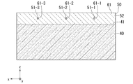
- FIG. 2 is a cross-sectional view of the incident surface of the PLC of the integrated optical device shown in FIG.
- FIG. 3 is a plan view of a part of the integrated optical device shown in FIG.
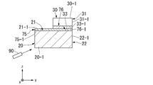
- FIG. 4 is a cross-sectional view taken along the line AA'in the integrated optical device shown in FIG.
- FIG. 5A is a cross-sectional view for explaining an example of a method for manufacturing the integrated optical device shown in FIG.
- FIG. 5B is a cross-sectional view for explaining an example of a method for manufacturing the integrated optical device shown in FIG.
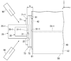
- FIG. 6 is a plan view for explaining a method of manufacturing the integrated optical device shown in FIG. FIG.
- FIG. 7 is a graph showing the relationship between the distance between the LD exit surface of the integrated optical device shown in FIG. 1 and the incident surface of the PLC and the light utilization efficiency.
- FIG. 8 is a plan view showing a state in which the LD of the integrated optical device shown in FIG. 1 is wire-bonded.
- FIG. 9 is a cross-sectional view showing a modified example of the integrated optical device of FIG.
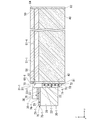
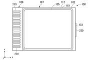
- FIG. 10 is a plan view of the integrated light source device in which the integrated optical device shown in FIG. 1 is packaged.
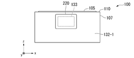
- FIG. 11 is a side view of the integrated light source device shown in FIG.
- FIG. 12 is a plan view of the integrated light source device shown in FIG. 10 with the cover removed.
- FIG. 13 is a side view of the integrated light source device shown in FIG. 10 as viewed from the exit side.
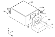
- FIG. 14 is a perspective view showing a form of the integrated light source device shown in FIG. 10 when used.
- the integrated optical device 10 of the present embodiment includes a subcarrier (base) 20, an LD (optical semiconductor element) 30 provided on the upper surface (surface) 21 of the subcarrier 20, and a substrate 40. And a PLC (optical waveguide) 50 provided on the upper surface (surface) 41 of the substrate 40.
- the integrated optical device 10 is a combiner that combines light of each of the three primary colors of light, red (R), green (G), and blue (B).
- the integrated optical device 10 can be applied as, for example, a combiner mounted on a head-mounted display.
- light having a peak wavelength of, for example, 610 nm or more and 750 nm or less can be used as red light.
- green light light having a peak wavelength of, for example, 500 nm or more and 560 nm or less can be used.
- blue light light having a peak wavelength of, for example, 435 nm or more and 480 nm or less can be used.
- the integrated optical device 10 includes an LD30-1 that emits red light, an LD30-2 that emits green light, and an LD30-3 that emits blue light.
- the LD30-1, 30-2, and 30-3 are arranged at intervals from each other in a direction substantially orthogonal to the emission direction of the light emitted from each LD.
- LD30-1, 30-2, 30-3 are provided on the upper surface 21 of the individual subcarriers 20.
- the LD30-1 is provided on the upper surface 21-1 of the subcarrier 20-1.
- the LD30-2 is provided on the upper surface 21-2 of the subcarrier 20-2.
- the LD30-3 is provided on the upper surface 21-3 of the subcarrier 20-3.
- reference numerals Z of any component of the integrated optical device 10 will be collectively referred to as reference numeral Z with respect to the contents common to the components of reference numerals Z-1, Z-2, ..., ZK. In some cases.
- the above-mentioned K is a natural number of 2 or more.
- the LD30 is mounted on the subcarrier 20 with a bare chip.
- the subcarrier 20 is made of, for example, aluminum nitride (AlN), aluminum oxide (Al 2 O 3 ), silicon (Si), or the like.
- a fourth metal layer (other metal layer) 75 and a fifth metal layer (other metal layer) 76 are provided between the subcarrier 20 and the LD30.
- the LD 30 is connected to the sub carrier 20 via a fourth metal layer 75 in contact with the sub carrier 20 and a fifth metal layer 76 in contact with the LD 30.
- the subcarrier 20-1 and the LD30-1 are connected to each other in the z direction via the fourth metal layer 75-1 and the fifth metal layer 76-1.
- the method of forming the fourth metal layer 75 and the fifth metal layer 76 is not specified.
- a known method can be applied, and for example, a known method such as sputtering, vapor deposition, or coating of a pasted metal can be applied.
- the fourth metal layer 75 is, for example, an alloy of gold (Au) and tin (Sn), an alloy of tin (Sn) and copper (Cu), an alloy of indium (In) and bismuth (Bi), and tin (Sn).
- )-Silver (Ag) -Copper (Cu) -based solder alloy (SAC) is composed of any alloy selected from the group.
- the fifth metal layer 76 is one or more metals selected from the group consisting of, for example, gold (Au), platinum (Pt), silver (Ag), lead (Pb), indium (In) and nickel (Ni). It is configured.
- the fourth metal layer 75 can be made of an alloy, and the fifth metal layer 76 can be made of a single metal.
- the fourth metal layer 75 and the fifth metal layer 76 are provided between the subcarrier 20 and the LD30, but even if one or more metal layers are provided between the subcarrier 20 and the LD30. Good.
- a fourth metal layer 75 and a fifth metal layer 76 are provided between the subcarrier 20 and the LD30 for the purpose of improving the reliability of the integrated optical device 10, and further between the subcarrier 20 and the fourth metal layer 75. May be provided with a metal layer.
- the metal layer provided between the subcarrier 20 and the fourth metal layer 75 is composed of one or more metals selected from the group consisting of, for example, titanium (Ti), tantalum (Ta) and tungsten (W).
- the substrate 40 is made of silicon (Si).
- the PLC 50 is formed on the upper surface 41 of the substrate 40 by a known semiconductor process including photolithography and dry etching used when forming a fine structure such as an integrated circuit. It is made to be one.
- the PLC50 includes a plurality of cores 51-1, 51-2, 51-3, which are the same number as LD30-1, 30-2, 30-3, and a clad 52 surrounding the cores 51-1, 51-2, 51-3. Is provided.
- the thickness of the clad 52 and the widthwise dimensions of the cores 51-1, 51-2, and 53-1 are not particularly limited. For example, cores 51-1, 51-2, 51-3 having dimensions in the width direction of about several microns are formed in the clad 52 having a thickness of about 50 ⁇ m.
- the cores 51-1, 51-2, 53-1 and the clad 52 are made of, for example, quartz.
- the refractive index of the cores 51-1, 51-2, 51-3 is higher than the refractive index of the clad 52 by a predetermined value.
- Light incident on each of the cores 51-1, 51-2, and 53-1 propagates through each core while being totally reflected at the interface between each of the cores 51-1, 51-2, and 53-1 and the clad 52.
- the cores 51-1, 51-2, and 51-3 are doped with impurities such as germanium (Ge) in an amount corresponding to the above-mentioned predetermined value.
- the emission direction of the light emitted from the LD30 (that is, the direction along the optical axis) is defined as the y direction.
- the direction in which the LD30-1, 30-2, and 30-3 are arranged at intervals from each other in the plane including the y direction is defined as the x direction.
- the direction orthogonal to the x-direction and the y-direction and from the subcarrier 20 to the LD30 is defined as the z-direction.
- the cores 51-1, 51-2, 51-3 are arranged along the optical axis of the light emitted from the LD30-1, 30-2, 30-3 in the x and z directions. ing.
- the cores 51-1, 51-2, and 53-1 are gathered together on the front side of reaching the exit surface 64 of the PLC 50.
- the cores 51-1, 51-2, and 51-3 approach each other in sequence toward the front in the y direction and join one core 54-1.
- the cores 51-1, 51-2, and 53-1 have a radius of curvature equal to or greater than a predetermined radius of curvature, respectively, so that light leakage from the cores 51-1, 51-2, and 53-1 does not occur. It is preferable to be connected to.
- the incident surface 61 of the PLC 50 is arranged so as to face the exit surface 31 of the LD 30. More specifically, the exit surface 31-1 of the LD30-1 faces the entrance surface 61-1 of the core 51-1. In the x-direction and the z-direction, the optical axis of the red light emitted from the LD30-1 and the center of the incident surface 61-1 substantially overlap. Similarly, the exit surface 31-2 of the LD30-2 faces the entrance surface 61-2 of the core 51-2. In the x-direction and the z-direction, the optical axis of the green light emitted from the LD30-2 and the center of the incident surface 61-2 substantially overlap.
- the exit surface 31-3 of the LD30-3 faces the entrance surface 61-3 of the core 51-3.
- the optical axis of the blue light emitted from the LD30-3 and the center of the incident surface 61-3 substantially overlap.
- the red light, green light, and blue light emitted from the LD30-1, 30-2, and 30-3 are incident on the cores 51-1, 51-2, and 51-3, respectively, and then each of them. Propagate the core.
- the red and green lights propagating through the cores 51-1 and 51-2 and the cores 51-1 and 51-2 meet at the confluence position 57-1 (see FIG. 3).
- the red light, green light, and blue light propagating through the cores 51-7 (see FIG. 3) and the cores 51-3, and the cores 51-3 and 51-7, in which the cores 51-1 and 51-2 are merged, merge.
- the merging position 57-2 is ahead of the merging position 57-1 in the y direction.
- the red light, green light, and blue light collected at the confluence position 57-2 propagate through the core 51-4 and reach the exit surface 64.
- the three-color light emitted from the exit surface 64 is used, for example, as signal light or the like depending on the purpose of use of the integrated optical device 10.
- the subcarrier 20 is connected to the substrate 40 via the first metal layer (metal layer) 71, the second metal layer (metal layer) 72, and the third metal layer (metal layer) 73.
- the side surface 22 (22-1, 22-1, 22-3) of the subcarrier 20 facing the substrate 40 and the side surface 42 of the substrate 40 facing the subcarrier 20 are the first metal layer 71.
- the second metal layer 72, the third metal layer 73, and the antireflection film 81 are connected to each other.
- the melting point of the fourth metal layer 75 is higher than the melting point of the third metal layer 73.
- the exit surface 31 of the LD 30 is arranged at substantially the same position as the side surface 22 of the subcarrier 20 in the y direction, that is, in the direction along the optical axes of red light, green light, and blue light emitted from the LD 30. ..
- the exit surface 31 of the LD 30 substantially overlaps the side surface 22 of the subcarrier 20 in the y direction, and forms a surface substantially identical to the side surface 22 of the subcarrier 20.
- the exit surface 31 of the LD 30 is substantially at the same position as the side surface 22 of the subcarrier 20 in the y direction
- the difference between the exit surface 31 of the LD 30 and the side surface 22 of the subcarrier 20 in the y direction is 0 ⁇ m or more and 10 ⁇ m. It is 0 ⁇ m or more and 5 ⁇ m or less, more preferably 0 ⁇ m or more and 2 ⁇ m or less, and particularly preferably 0 ⁇ m.
- the light emitted from the LD 30 is the corner portion of the subcarrier 20 on the back side in the y direction and the back side in the z direction. There is a risk that the amount of light incident on the PLC 50 will decrease.
- the exit surface 31 of the LD 30 is located at substantially the same position as the side surface 22 of the subcarrier 20 in the y direction, the bonding strength between the LD 30 and the subcarrier 20 is increased, and the reliability of the integrated optical device 10 is improved. improves.
- the first metal layer 71 is provided in a state of being in contact with the side surface 22 by sputtering, vapor deposition, or the like, and is, for example, gold (Au), platinum (Pt), silver (Ag), lead (Pb), indium (In), nickel. It is composed of one or more metals selected from the group consisting of (Ni), titanium (Ti) and tantalum (Ta).
- the first metal layer 71 is composed of any metal selected from the group consisting of gold (Au), platinum (Pt), silver (Ag), lead (Pb), indium (In) and nickel (Ni). Is preferable.
- the second metal layer 72 is provided in a state of being in contact with the side surface 42 by sputtering, vapor deposition, or the like, and is one or a plurality of metals selected from the group consisting of, for example, titanium (Ti), tantalum (Ta), and tungsten (W). It is composed of.
- the third metal layer 73 is interposed between the first metal layer 71 and the second metal layer 72, and is selected from the group consisting of, for example, AuSn, SnCu, InBi, SnAgCu, SnPdAg, SnBiIn and PbBiIn. It is composed of an alloy.
- the third metal layer 73 is preferably composed of any alloy selected from the group consisting of AuSn, SnAgCu and SnBiIn. As described above, the first metal layer 71 and the second metal layer 72 can be made of a single metal, the third metal layer 73 can be made of an alloy, and the subcarrier 20 and the substrate 40 can be made of a single metal. Can be joined with an alloy.
- an alloy having a melting point in the range of 250 ° C. to 500 ° C. can be used as the fourth metal layer 75.
- the third metal layer 73 an alloy having a melting point in the range of 200 ° C. to 490 ° C. can be used.
- the difference between the melting point of the layer between the subcarrier 20 and the LD30 and the melting point of the layer between the subcarrier 20 and the substrate 40 is at least different.
- the melting point of the fourth metal layer 75 is preferably 20 ° C. or higher, more preferably 30 ° C. or higher, higher than the melting point of the third metal layer 73.
- the thickness of the first metal layer 71 that is, the size of the first metal layer 71 in the y direction is, for example, 0.01 ⁇ m or more and 5.00 ⁇ m or less.
- the thickness of the second metal layer 72 that is, the size of the second metal layer 72 in the y direction is, for example, 0.01 ⁇ m or more and 1.00 ⁇ m or less.
- the thickness of the third metal layer 73 that is, the size of the third metal layer 73 in the y direction is, for example, 0.01 ⁇ m or more and 5.00 ⁇ m or less. Further, the thickness of the third metal layer 73, that is, the size along the y direction is preferably larger than the thicknesses of the first metal layer 71 and the second metal layer 72.
- the roles of the first metal layer 71, the second metal layer 72, and the third metal layer 73 are well expressed, the material of the first metal layer 71 enters the substrate 40, and the metal layers are connected to each other. The decrease in adhesive strength is suppressed.
- the first metal layer 71 is provided on the side surface facing the substrate 40 or the PLC 50 in substantially the entire area of the side surface 22 within a range not in contact with the fourth metal layer 75.
- the front end that is, the upper end of the second metal layer 72 and the third metal layer 73 in the z direction reaches the same position as the first metal layer 71 on the front side in the z direction.
- the rear end that is, the lower end of the second metal layer 72 and the third metal layer 73 in the z direction reaches a position behind the first metal layer 71 and in front of the antireflection film 81.
- the first metal layer 71 is formed larger than the subcarrier 20 in the x direction.
- the area of the first metal layer 71 that is, the in-plane size including the x-direction and the z-direction is substantially the same as the area of the second metal layer 72 and the third metal layer 73. Alternatively, it is preferably smaller than the areas of the second metal layer 72 and the third metal layer 73. In the above configuration, the connection strength of the subcarrier 20 to the substrate 40 is secured to the maximum.
- an antireflection film 81 is provided between the LD 30 and the PLC 50.
- the antireflection film 81 is integrally formed with the side surface 42 of the substrate 40 and the incident surface 61 of the PLC 50.
- the antireflection film 81 may be formed only on the incident surface 61 of the PLC 50.
- FIG. 1 shows a schematic configuration of the integrated optical device 10, and the first metal layer 71, the second metal layer 72, the third metal layer 73, and the antireflection films 81 and 82 are omitted.
- the antireflection films 81 and 82 prevent the incident light or the emitted light from the PLC 50 from being reflected from the incident surface 61 or the exit surface 64 in the direction opposite to the direction of entering each surface, and transmit the incident light or the emitted light. It is a film for increasing the rate.
- the antireflection films 81 and 82 are multilayer films formed by alternately laminating a plurality of types of dielectrics with a predetermined thickness according to the wavelengths of incident light such as red light, green light, and blue light. is there.
- the aforementioned dielectrics are, for example, titanium oxide (TiO 2 ), silicon oxide (SiO 2 ), aluminum oxide (Al 2 O 3 ) and the like.
- the exit surface 31 of the LD30 and the incident surface 61 of the PLC50 are arranged at a predetermined interval (see FIG. 6).
- the incident surface 61 faces the exit surface 31.
- In the y direction there is a gap 70 between the exit surface 31 and the entrance surface 61.
- the gap 70 is filled with air.
- the size of the gap 70 in the y direction is, for example, larger than 0 ⁇ m and 5 ⁇ m or less. is there. The relationship between the size of the gap 70 in the y direction and the light utilization efficiency of red light, green light, and blue light will be described later.
- 5A and 5B are cross-sectional views for explaining an example of the manufacturing method of the integrated optical device 10 shown in FIG.
- the bare chip LD30 is mounted on the upper surface 21 of the subcarrier 20 by a known method.
- the fourth metal layer 75 is formed on the upper surface 21 of the subcarrier 20 by sputtering or vapor deposition, and the fifth metal layer 76 is further sputtered on the lower surface 33 of the LD30 (for example, the lower surface 33-1 of the LD30-1).
- it is formed by vapor deposition or the like.
- a metal layer may be formed on the upper surface 21 of the subcarrier 20 by sputtering or vapor deposition, and then a fourth metal layer 75 may be formed on the metal layer by sputtering or vapor deposition.
- the subcarrier 20 is irradiated with laser light from the laser 90, only the subcarrier 20 is heated to the extent that it does not melt and deform, and the fourth metal is transferred by heat transfer from the subcarrier 20.
- the layer 75 and the fifth metal layer 76 are softened or melted, and then cooled.
- the LD 30 is joined to the upper surface of the subcarrier 20 via the fourth metal layer 75 and the fifth metal layer 76.
- a first metal layer 71 is formed on the side surface 22 of the subcarrier 20 by sputtering, vapor deposition, or the like.
- PLC50 is formed on the upper surface 41 of the substrate 40 by a known semiconductor process. Subsequently, antireflection films 81 and 82 and antireflection films (not shown) are formed on the entrance surface 61 and the exit surface 64. After that, the second metal layer 72 and the third metal layer 73 are formed in this order behind the antireflection film 81 in the y direction by sputtering, vapor deposition, or the like.
- the LD30 corresponding to each other, the exit surface 31 of the cores 51-1, 51-2, and 53-1 and the incident surface 61 are opposed to each other with a space in the y direction.
- the optical axis of each color light emitted from the LD 30 and the center of the incident surface 61 of the corresponding core are substantially overlapped.
- the subcarrier 20 is irradiated with laser light from the laser 90, and the first metal layer 71, the second metal layer 72, and the third metal layer 73 are softened by heat transfer from the subcarrier 20. Alternatively, it is melted and the subcarrier 20 on which the LD30 is mounted is bonded to the substrate 40 on which the PLC50 is formed while adjusting the relative positions of the LD30 and the PLC50.
- lasers 90 are arranged on both sides of the subcarrier 20 in the X direction.
- the light emitted from the laser 90 is applied to the subcarrier 20 along the direction indicated by the arrow in FIG. 6 to heat the subcarrier 20, and only the subcarrier 20 is heated to such an extent that it is not melted or deformed.
- each color light is emitted from the LD30, the emission intensity is detected, and the emission intensity of the three color lights emitted from the core 51-4 is detected.
- the positions and orientations of the intervals S and LD30 are adjusted so as to satisfy the required light utilization efficiency.
- the adjustment of the position and posture of the LD30 described above means that so-called active alignment and gap control are performed.
- the above-mentioned adjustment of the interval S and LD30 can be performed using a known device having an active alignment function.
- the first metal layer 71 and the second metal layer 71 between the exit surface 31 and the entrance surface 61 of the LD 30 arranged at the optimum positions are performed.
- the metal layer 72 and the third metal layer 73 become thinner than the respective metal layers not sandwiched between the exit surface 31 and the entrance surface 61 due to the alloying of the third metal layer 73 and slight heat shrinkage. It is cooled by stopping the heating of the subcarrier 20 by the laser 90, and the position of the LD 30 is fixed. By proceeding with the above procedure, the integrated optical device 10 can be manufactured.
- the above-mentioned integrated optical device 10 may be housed in, for example, a package 110 as shown in FIGS. 10 and 11.
- the packaged integrated light source device 100 includes the above-mentioned integrated optical device 10 and the package 110.
- the package 110 includes a main body 102 having a cavity structure and a cover 105 that covers the main body 102.
- the main body 102 has a box-shaped accommodating portion 107 in which the integrated optical device 10 is accommodated, and an electrode portion 108 adjacent to the accommodating portion 107.
- the main body 102 is made of, for example, ceramic or the like.
- An opening is formed on the upper surface of the accommodating portion 107.
- a metal film 112 is formed on the upper surface of the accommodating portion 107 at the periphery of the opening when viewed from above.
- the cover 105 covers the opening formed on the upper surface of the accommodating portion 107 without a gap through the metal film 112.
- an inert gas such as nitrogen (N 2 ) is sealed in the internal space of the accommodating portion 107. That is, the accommodating portion 107 is hermetically sealed by the cover 105.
- the internal space of the accommodating portion 107 is filled with an inert gas.
- the electrode portion 108 is arranged on the front side in the y direction of the accommodating portion 107, that is, on the rear side in the y direction.
- the upper surface of the electrode portion 108 is located below the upper surface of the accommodating portion 107.
- the bottom surface of the electrode portion 108 is located at substantially the same height as the bottom surface of the accommodating portion 107.
- a plurality of external electrode pads 210 are provided on the upper surface of the electrode portion 108 at intervals in the x direction.
- a base 180 for installing the integrated optical device 10 is provided at a predetermined position on the bottom wall portion 131 of the accommodating portion 107.
- the integrated optical device 10 is provided on the base 180. That is, the integrated optical device 10 is arranged in the internal space of the accommodating portion 107.
- the bottom surfaces of the subcarrier 20 and the substrate 40 of the integrated optical device 10 are in contact with the upper surface of the base 180.
- a plurality of internal electrode pads 202 are provided on the bottom wall 131 located between the base 180 below the subcarrier 20 and the external electrode pads 210 in the y direction at intervals in the x direction.
- Each of the LD30 and the subcarrier 20 and the internal electrode pad 202 corresponding to each LD30 among the plurality of internal electrode pads 202 are connected by a wire 95 using a method such as wire bonding.
- a method such as wire bonding.
- each of the LD30-1 and the subcarrier 20-1 and each of the two internal electrode pads 202-1 are individually connected by a wire 95-1.
- Each of the LD30-2 and the subcarrier 20-2 and each of the two internal electrode pads 202-2 are individually connected by a wire 95-2.
- Each of the LD30-3 and the subcarrier 20-3 and each of the two internal electrode pads 202-3 are individually connected by a wire 95-3.
- Each of the internal electrode pads 202-1, 202-2, and 202-3 is connected to external electrode pads 210 that are different from each other.
- the external electrode pad 210 electrically connected to each of the internal electrode pads 202-1202-2 and 202-3 is electrically connected to a power source or the like (not shown). That is, in the integrated light source device 100, the LD 30 and the power supply (not shown) are connected by a wire 95, internal electrode pads 202-1, 202-2, 202-3, and an external electrode pad 210.
- the LD30-1, 30-2, and 30-3 are red. Light, green light, and blue light are emitted.
- an opening 133 is formed in the side wall 132 facing the exit surface 31 of the PLC 50 of the integrated optical device 10.
- the opening 133 is formed around a position intersecting the optical axis of the three-color light emitted from the core 51-4 of the PLC 50 on the side wall portion 132.
- the opening 133 is formed to be larger than the size on the surface of the side wall portion 132 of the three-color light that is emitted from the core 51-4 and spreads in the internal space of the accommodating portion 107.
- the opening 133 is covered by the glass plate 220 from the outside of the side wall portion 132 without any gap. That is, the accommodating portion 107 is hermetically sealed by a glass plate 220 in addition to the cover 105. Antireflection films (not shown) are provided on both surface of the glass plate 220.
- the opening 133 is a window through which the three-color light emitted from the core 51-4 of the PLC 50 passes and propagates to the outside of the package 110.
- the three-color light LL emitted from the core 51-4 of the PLC 50 passes through the opening 133 and the glass plate 220 while diffusing around the y direction, and is the back side in the y direction of the package 110, that is, Proceed forward in the y direction.
- the collimating device 300 provided with the collimating lens 310 can be arranged behind the side wall portion 132-1 of the package 110 in the y direction.
- the distance between the exit surface 31 and the collimating lens 310 in the y direction is matched with the focal length of the collimating lens 310, and the center of the collimating lens 310 is aligned with the optical axis of the three-color light LL.
- the colored light LL is collimated to become parallel light.
- the integrated optical device 10 described above includes a subcarrier 20, an LD30, a substrate 40, and a PLC50.
- the incident surface 61 is arranged so as to face the exit surface 31, and the light emitted from the LD 30 can enter the cores 51-1, 51-2, and 53-1.
- the side surface 22 of the subcarrier 20 and the side surface 42 of the substrate 40 are connected from the rear to the front in the y direction via the first metal layer 71, the second metal layer 72, and the third metal layer 73.
- the first metal layer 71 and the second metal layer 72 are firmly adhered to the side surface 22 and the side surface 42, and the third metal layer 73 is an interface with the first metal layer 71 and the second metal layer 72.
- the side surface 22 is firmly joined to the first metal layer 71 and the second metal layer 72 in substantially the entire area including the x direction and the z direction.
- the connection between the subcarrier 20 and the substrate 40 by the first metal layer 71, the second metal layer 72, and the third metal layer 73 by such alloying is resistant to heat, for example, wire bonding or the like as shown in FIG. It is difficult to release even if the ambient temperature rises in the process.
- the integrated optical device 10 can exhibit desired light utilization efficiency and optical characteristics, and the reliability of the integrated optical device 10 can be enhanced.
- the third metal layer 73 is thicker than the first metal layer 71 and the second metal layer 72, the first metal layer 71 and the third metal layer 73, and / or the third metal layer 73 And the second metal layer 72 are sufficiently alloyed, and the subcarrier 20 and the substrate 40 can be joined more firmly. According to the integrated optical device 10, the distance between the alloy layer of the first metal layer 71 and the third metal layer 73 and the substrate 40 can be secured in the y direction.
- the area of the first metal layer 71 is smaller than the area of the second metal layer 72 when viewed along the y direction (the traveling direction of light), so that the subcarrier 20 and the substrate 40 It is possible to secure at least the area of the first metal layer 71 or more.
- the bonding area of the subcarrier 20 can be maximized, and the subcarrier 20 and the substrate 40 can be bonded more firmly.
- the antireflection film 81 is provided between the LD 30 and the PLC 50, it is possible to prevent the reflection of each color light emitted from the LD 30 on the incident surface 61, and the core 51- of each color light can be prevented.
- the binding efficiency to 1,51-2,51-3 can be increased.
- the integrated optical device 10 since the exit surface 31 of the LD 30 and the incident surface 61 of the PLC 50 are arranged at a predetermined interval, the conventional integrated optics in which a resin is interposed between the exit surface of the LD and the incident surface of the PLC. Unlike the device, the relative arrangement of the LD and the PLC is not affected by the inclusions between the exit surface of the LD and the entrance surface of the PLC. According to the integrated optical device 10, it is possible to prevent the occurrence of a deviation in the relative arrangement between the LD 30 and the PLC 50.
- the integrated optical device 10 includes a plurality of LD30s, and the plurality of LD30s emit light having peak wavelengths (wavelengths) different from each other. That is, the integrated optical device 10 includes a plurality of LD30-1, 30-2, 30-3.
- the PLC 50 is provided with a plurality of cores 51-1, 51-2, 51-3 capable of incident light emitted by a plurality of LD30-1, 30-2, 30-3, and a plurality of cores 51-1. , 51-2 and 51-3 are gathered together on the front side reaching the exit surface 64.
- three-color light having different peak wavelengths (wavelengths) is efficiently incident on a plurality of cores 51-1, 51-2, 51-3, and the three-color light emitted from the emission surface 64 is emitted. Light utilization efficiency can be improved.
- the integrated optical device 10 includes a subcarrier 20, an LD30, a substrate 40, and a PLC50.
- the incident surface 61 is arranged so as to face the exit surface 31, and the light emitted from the LD 30 can enter the cores 51-1, 51-2, and 53-1.
- the subcarrier 20 is connected to the substrate 40 via the first metal layer 71, the second metal layer 72, and the third metal layer 73.
- the LD30 is connected to the subcarrier 20 via the fourth metal layer 75 and the fifth metal layer 76.
- the melting points of the fourth metal layer 75 and the fifth metal layer 76 are higher than the melting points of the first metal layer 71, the second metal layer 72, and the third metal layer 73.
- the LD 30 is connected to the subcarrier 20 via the fourth metal layer 75 and the fifth metal layer 76, and the subcarrier 20 is connected to the first metal layer 71, the second metal layer 72, and the third metal layer 73. It is connected to the substrate 40 via.
- the melting point of the fourth metal layer 75 is higher than the melting point of the third metal layer 73.
- the fourth metal layer 75 and the fifth metal layer 76 are melted or softened to bond the LD30 and the subcarrier 20, and then the first metal layer 71 and the second metal layer are joined.
- the fourth metal layer 75 is remelted and a relative misalignment between the LD 30 and the subcarrier 20 occurs. Can be prevented.
- the positional accuracy between the LD 30 and the PLC 50 connected via the sub carrier 20 can be improved, and a highly reliable integrated optical device 10 can be provided.
- the fourth metal layer 75 and the fifth metal layer 76 are firmly bonded to the upper surface 21 and the lower surface 33 while alloying at or near these interfaces.
- the first metal layer 71 and the second metal layer 72 are firmly joined to the side surface 22 and the side surface 42.
- the third metal layer 73 is alloyed at or near the interface with the first metal layer 71 and at or near the interface with the second metal layer 72, and is a surface including the x-direction and the z-direction of the side surface 22. It is firmly joined to the first metal layer 71 and the second metal layer 72 in substantially the entire area.
- the connection between the subcarrier 20 and the substrate 40 by the first metal layer 71, the second metal layer 72, and the third metal layer 73 by the alloying described above is resistant to heat, and is a step such as wire bonding as shown in FIG. It is difficult to release even if the ambient temperature rises. Therefore, even when the LD 30 and the power supply (not shown) are connected by the wire 95 on the upper surface 21 by a method such as wire bonding, the state in which the PLC 50 is firmly fixed to the LD 30 is maintained. As described above, during wire bonding, the LD 30 and the subcarrier 20 do not slide off the PLC 50 and the substrate 40, and the LD 30 is maintained at an optimum position with respect to the PLC 50. As a result, the integrated optical device 10 can exhibit desired light utilization efficiency and optical characteristics, and the reliability of the integrated optical device 10 can be enhanced.
- the third metal layer 73 is thicker than the first metal layer 71 and the second metal layer 72, the first metal layer 71 and the third metal layer 73, and / or the third metal layer 73 And the second metal layer 72 are sufficiently alloyed, and the subcarrier 20 and the substrate 40 can be joined more firmly. According to the integrated optical device 10, the distance between the alloy layer of the first metal layer 71 and the third metal layer 73 and the substrate 40 is secured in the y direction.
- the area of the first metal layer 71 is smaller than the area of the second metal layer 72 when viewed along the y direction (the traveling direction of light), so that the subcarrier 20 and the substrate 40 It is possible to secure at least the area of the first metal layer 71 or more.
- the bonding area of the subcarrier 20 can be maximized, and the subcarrier 20 and the substrate 40 can be bonded more firmly.
- the antireflection film 81 is provided between the LD 30 and the PLC 50, it is possible to prevent the reflection of each color light emitted from the LD 30 on the incident surface 61, and the core 51- of each color light can be prevented.
- the binding efficiency to 1,51-2,51-3 can be increased.
- the integrated optical device 10 includes a plurality of LD30s, and the plurality of LD30s emit light having peak wavelengths (wavelengths) different from each other. That is, the integrated optical device 10 includes a plurality of LD30-1,30-2,30-3 clothes, and the light emitted by the plurality of LD30-1, 30-2, 30-3 can be incident on the PLC50.
- a plurality of cores 51-1, 51-2, 51-3 are provided, and the plurality of cores 51-1, 51-2, 51-3 are gathered together on the front side reaching the exit surface 64. There is.
- three-color light having different peak wavelengths (wavelengths) is efficiently incident on a plurality of cores 51-1, 51-2, 51-3, and the three-color light emitted from the emission surface 64 is emitted.
- Light utilization efficiency can be improved.
- the color of light emitted from the LD30 which is the light source used in the integrated optical device 10 according to the present invention, is not limited to red (R), green (G), and blue (B), and colors other than these colors are used. It may be.
- light other than red (R), green (G), and blue (B) can also be used.
- the mounting order (that is, mounting position) of the red (R), green (G), and blue (B) LD30s in the integrated optical device 10 described with reference to the drawings also needs to be the mounting order illustrated in the drawings. However, it can be changed as appropriate from the mounting order illustrated in the drawing.
- the subcarrier 20 and the LD30 may be connected via a metal composite layer (not shown) including an alloy layer of at least the fourth metal layer 75 and the fifth metal layer 76.
- the "metal composite layer including at least the alloy layer of the fourth metal layer 75 and the fifth metal layer 76" has an alloy layer of the fourth metal layer 75 and the fifth metal layer 76 as a part of the metal composite layer. It means a layer that is formed or a layer in which the entire metal composite layer is composed of the alloy layer.
- the metal of the fourth metal layer 75 and the metal of the fifth metal layer 76 may be alloyed over a part or the whole in the z direction to form an alloy layer.
- the fourth metal layer 75 and the metal of the fifth metal layer 76 are partially alloyed in the z direction, the fourth metal layer 75 and the fifth metal layer are sandwiched between the subcarrier 20 and the LD30.
- the alloy layer of 76 and either or both of the fourth metal layer 75 and the fifth metal layer 76 intervene.
- the metal of the fourth metal layer 75 and the metal of the fifth metal layer 76 are alloyed over the entire z direction, substantially only the above alloy layer is interposed between the subcarrier 20 and the LD. To do.
- the fourth metal layer 75 and the fifth metal layer 76 are alloyed over the entire y-direction of the fifth metal layer 76, and the fourth metal layer 75 It is preferable that an alloy layer of and the fifth metal layer 76 is formed. However, the fourth metal layer 75 and the fifth metal layer 76 may be alloyed at a part of the fifth metal layer 76 in the y direction to form the alloy layer.
- the subcarrier 20 and the substrate 40 are at least an alloy layer of the metal of the first metal layer 71 and the third metal layer 73, and / or the metal of the second metal layer 72 and the third metal layer 73. It may be connected via another metal composite layer (not shown) including an alloy layer with. What is "another metal composite layer including at least an alloy layer of the metal of the first metal layer 71 and the third metal layer 73 and / or an alloy layer of the metal of the second metal layer 72 and the third metal layer 73"? , And / or has an alloy layer of the metal of the first metal layer 71 and the third metal layer 73, and / or an alloy layer of the second metal layer 72 and the third metal layer 73, or a part thereof.
- All of them mean a layer composed of an alloy layer of the metal of the first metal layer 71 and the third metal layer 73, and an alloy layer of the metal of the second metal layer 72 and the third metal layer 73.
- the metal of the first metal layer 71 and the metal of the third metal layer 73 may be alloyed over a part or the whole in the y direction to form one alloy layer.
- the metal of the second metal layer 72 and the metal of the third metal layer 73 may be alloyed over a part or the whole in the y direction to form one alloy layer.
- the subcarrier 20 and the substrate 40 are made of either or both of the alloy layer of the first metal layer 71 and the third metal layer 73 and the alloy layer of the second metal layer 72 and the third metal layer 73. Can be connected via.
- the melting point of the metal composite layer including the alloy layer of the fourth metal layer 75 and the fifth metal layer 76 is the alloy layer of the first metal layer 71 and the third metal layer 73, and the second metal layer 72 and the third metal layer. It is higher than the melting point of other metal composite layers including the alloy layer with 73.
- the melting point of the alloy constituting the alloy layer of the metal constituting the fourth metal layer 75 and the metal constituting the fifth metal layer 76 constitutes the metal constituting the first metal layer 71 and the third metal layer 73.
- the melting point of the alloy forming the alloy layer of the metal forming the fourth metal layer 75 and the metal forming the fifth metal layer 76 is the metal forming the second metal layer 72 and the metal forming the third metal layer 73. It is higher than the melting point of the alloy constituting the alloy layer with.
- an integrated optical device 10 having high positional accuracy and high reliability between the LD 30 and the PLC 50 connected via the subcarrier 20.
- the reliability of the integrated optical device 10 can be improved by connecting the subcarrier 20 and the substrate 40 more firmly with an alloy layer than with the conventional resin connection.
- the melting point of the alloy layer formed at or near the interface of each metal layer depends on the melting point of the fourth metal layer 75 or the third metal layer 73. For example, by forming the fourth metal layer 75 thicker than the fifth metal layer 76, or by forming the third metal layer 73 thicker than the first metal layer 71 and the second metal layer 72, each metal layer can be formed. The melting point of the alloy layer formed at or near the interface can be easily controlled.
- the metal material interposed between the subcarrier 20 and the substrate 40 for connecting them can be appropriately changed depending on the materials of the subcarrier 20, the substrate 40, and the first metal layer 71.
- the thickness of the metal material of the metal layer or the alloy layer can be appropriately set according to each material of the subcarrier 20, the substrate 40, and the first metal layer 71.
- the configuration of the metal composite layer interposed between the subcarrier 20 and the substrate 40 may change depending on the type and thickness of the metal material, the heating conditions of the subcarrier 20, and the like.
- the metal composite layer may be a single alloy layer, a combination of a metal layer and an alloy layer, a combination of alloy layers having different compositions from each other, or a multilayer structure different from the above combination and including at least an alloy layer. ..
- the subcarrier 20 and the LD30 are connected to each other via the fourth metal layer 75 and the fifth metal layer 76, but the subcarrier 20 and the LD30 are connected to one metal layer (for example, the fourth metal). It may be connected only through layer 75 (75-1)).
- the subcarrier 20 and the substrate 40 are connected via the first metal layer 71, the second metal layer 72, the third metal layer 73, and the antireflection film 81, but one metal layer. It may be connected only through.
- the side surface 22 of the subcarrier 20 facing the substrate 40 and the side surface 42 of the substrate 40 facing the subcarrier 20 are formed by the first metal layer 71, the second metal layer 72, and the third metal layer 73. It is connected via an antireflection film 81.
- the configuration between the side surface 22 of the subcarrier 20 and the side surface 42 of the substrate 40 is not limited to the laminated structure of the first metal layer 71, the second metal layer 72, the third metal layer 73, and the antireflection film 81. .. As shown in FIG.
- the lower surface 23 (23-1) of the subcarrier 20 facing the substrate 40 and the upper surface 41 of the substrate 40 facing the subcarrier 20 are formed by the first metal layer 71 and the second metal layer 72. It may be connected via the third metal layer 73. In this case, the melting point of the fourth metal layer 75 is higher than the melting point of the third metal layer 73.
- the subcarrier 20 and the substrate 40 are formed by at least an alloy layer of the metal of the first metal layer 71 and the third metal layer 73, and / or the metal of the second metal layer 72 and the third metal layer 73. It may be connected via another metal composite layer (not shown) including an alloy layer.
- the melting point of the fourth metal layer 75 is the alloy layer of the metal of the first metal layer 71 and the third metal layer 73 and / or the second metal layer 72 and the third metal layer 73. It is higher than the melting point of other metal composite layers including alloy layers.
- the gap 70 is filled with air.
- the integrated optical device 10 is housed in a housing (not shown), and the above-mentioned housing is filled with an inert gas such as nitrogen (N 2 ). May be good. That is, the gap 70 may be filled with the inert gas.
- N 2 nitrogen
- the configuration of the package 110 shown in FIGS. 10 to 14 can be appropriately changed according to the configuration and shape of the integrated optical device 10.
- the integrated optical device 10 is a combiner that combines light of three primary colors in the visible wavelength range.
- the integrated optical device according to the present invention is not limited to the combiner, and can be widely used in the field of optical communication and the like.
- the integrated optical device 10 can combine the three primary colors in the visible wavelength range for the purpose of being used in applications such as wearable devices and small projectors.
- the wavelength of light processed by the integrated optical device according to the present invention is not limited to the visible wavelength region.
- the wavelength range of light processed by the integrated optical device according to the present invention may range from the visible wavelength range to the near-infrared wavelength range, and may be only the near-infrared wavelength range for the purpose of being used in optical communication. Good.
- the materials of the substrate 40, the PLC50, various metal layers, and the alloy layer can be appropriately selected according to the wavelength of light processed by the integrated optical apparatus according to the present invention.
- Integrated optics 20 Subcarrier (base) 20-1 Subcarrier (base) 20-2 Subcarrier (base) 20-3 Subcarrier (base) 21 Top surface 21-1 Top surface 21-2 Top surface 21-3 Top surface 22 Side surface 22-1 Side surface 22-2 Side surface 22-3 Side surface 23 Bottom surface 23-1 Bottom surface 30 LD (optical semiconductor element) 30-1 LD 30-2 LD 30-3 LD 31 Exit surface 31-1 Exit surface 31-2 Exit surface 31-3 Exit surface 33 Bottom surface 33-1 Bottom surface 40 Substrate 41 Top surface (front surface) 42 Side 50 PLC (optical fiber) 51-1, 51-2, 53-1 Core 54-1, 51-7 Core 52 Clad 57-1, 57-2 Confluence position 61 Incident surface 61-1 Incident surface 61-2 Incident surface 61-2 Incident surface 64 Exit surface 70 Gap 71 First metal layer (metal layer) 71-1 1st metal layer 71-2 1st metal layer 71-3 1st metal layer 72 2nd metal layer (metal layer) 73 Third metal layer (metal layer) 75 Fourth metal layer
Landscapes
- Physics & Mathematics (AREA)
- General Physics & Mathematics (AREA)
- Optics & Photonics (AREA)
- Condensed Matter Physics & Semiconductors (AREA)
- Electromagnetism (AREA)
- Engineering & Computer Science (AREA)
- Microelectronics & Electronic Packaging (AREA)
- Optical Couplings Of Light Guides (AREA)
Abstract
本発明に係る集積光学装置は、基台と、前記基台の表面に設けられた光半導体素子と、基板と、前記基板の表面に設けられた光導波路と、を備える。前記光導波路の入射面は、前記光半導体素子の出射面と対向するように配置されている。前記光半導体素子から出射される光は、前記光導波路に入射可能である。前記基台において前記基板に対向する第1側面と前記基板において前記基台に対向する第2側面とは、金属層を介して接続されている。
Description
本発明は集積光学装置に関する。
本願は、2019年3月28日に、日本に出願された特願2019-062532号及び特願2019-062533に基づき優先権を主張し、その内容をここに援用する。
本願は、2019年3月28日に、日本に出願された特願2019-062532号及び特願2019-062533に基づき優先権を主張し、その内容をここに援用する。
データトラフィックの増大に伴い、光通信システムや、光通信システムを用いた身の回りの種々の光学装置の多機能化が進んでいる。最近では多機能化と共に高密度化が求められ、多機能且つ小型な光学装置が検討されている。
光通信システムに用いられるシリコン導波路に発光素子や受光素子を集積させるシリコンフォトニクスが進展している。光通信システムに用いられる代表的なシリコン導波路の1つが、合波・分波・波長選択等の光信号処理を行う平面光波回路(Planar Lightwave Circuit:PLC)である。
光通信システム以外の例えばウェアラブルデバイスや小型プロジェクタ等においても、使用目的に応じて複数の機能を発現し、且つ装置全体を持ち歩き可能とするために、多機能且つ小型な光学装置が求められている。
従来、複数の光学素子を1つに集積化するために、ミラー及びレンズが用いられている。例えば、特許文献1には、レーザーダイオード(Laser Diode:LD)、光学レンズ、全反射用波長フィルタ、波長分離用フィルタ、ファイバコリメータ、フォトダイオードが筐体内に集積された光モジュール(集積光学装置)が開示されている。特許文献1に開示されている光モジュールでは、LDから発せられた波長1.3μmの光が集光レンズ、キャピラリ、コリメータレンズ、全反射用波長フィルタを通り、波長分離用フィルタで全反射され、ファイバコリメータで受光される。ファイバコリメータから入力された波長1.49μm,1.55μmの光は、波長分離用フィルタを通った後、波長分離用フィルタにより互いに分離される。分離された波長1.55μmの光は、全反射用波長フィルタにより全反射され、結合レンズによりフォトダイオードに入射する。分離された波長1.49μmの光は、結合レンズによりフォトダイオードに入射する。
特許文献2に開示されている光送受信モジュール(集積光学装置)では、光素子搭載基板と光合分波器がパッケージ内に固定されている。光素子搭載基板は、実装基板に互いに異なる波長の光を発する第1及び第2の発光素子を実装したものである。光合分波器は、第1の波長選択フィルタと、第1の波長選択フィルタに対して所定の間隔をあけて且つ第1の波長選択と平行に向き合って設けられたミラーと、を有する。特許文献2に開示されている光送受信モジュールでは、第1の出射光は、第1の発光素子から出射され、光合分波器に入射し、ミラーで反射する。第2の出射光は、第2の発光素子から出射され、光合分波器に入射し、第1の出射光と合波する。特許文献2に開示されている光送受信モジュールでは、波長選択フィルタ及びミラーの配置に合わせて互いに異なる所定の波長を有する複数の光を入射させ、波長合分波器で合波できる。
特許文献1,2のようにミラーやレンズを集積化した装置とは別の構造を備える装置として、例えば特許文献3、4には導波路構造を備えた光デバイス(集積光学装置)が開示されている。特許文献3に開示されている合波器では、N本の薄いクラッドを有するファイバ素線がチップ型板に固定され、複数のファイバ素線の出射端が互いに束ねられている。任意の特許文献4には、半導体導波路を有する半導体チップと、PLCチップとを一体化したハイブリッド集積光モジュールが開示されている。半導体チップは、第1の基板上に搭載されている。
特許文献4に開示されているハイブリッド集積光モジュール(集積光学装置)では、半導体チップにおいてPLCチップに対向する端面とPLCチップにおいて半導体チップに対向する端面とは、間隔をあけて互いに離間している。半導体チップとPLCチップとは、紫外線硬化接着剤で接着されている。
しかしながら、上述の特許文献1、2に開示されている装置では、部品数が多く、個々の部品の設置スペースが必要であり、ミラーやレンズを用いて自由空間光学系で構成されている。そのため、特許文献1、2に開示されている装置では、小型化を図ることが難しい。特許文献3、4に開示されているように導波路を用いた光学装置では、部品同士が紫外線硬化樹脂等で接着されている。そのため、装置の製造時に、光源のワイヤーボンディングの工程で温度変化による紫外線硬化接着剤の膨張・収縮が生じると、互いに接着されていた部品同士の調芯精度が低下し、製造された装置の信頼性が低下する虞があった。特許文献3、4に開示されている装置では、LD等の光半導体素子を作動させるために、ワイヤーボンディング等の方法を用いて光半導体素子と電源とを基板上で導通させる。光半導体素子に対して光導波路が固定される強度が十分でないと、ワイヤーボンディングを行う際に、光半導体素子が光導波路や基板から落下する虞があった。
本発明は、信頼性の高い集積光学装置を提供する。
本発明に係る第1態様によれば、集積光学装置は、基台と、前記基台の表面に設けられた光半導体素子と、基板と、前記基板の表面に設けられた光導波路と、を備え、前記光導波路の入射面が前記光半導体素子の出射面と対向するように配置され、前記光半導体素子から出射される光が前記光導波路に入射可能であり、前記基台において前記基板に対向する第1側面と前記基板において前記基台に対向する第2側面とが金属層を介して接続されている。
本発明に係る第2態様によれば、集積光学装置は、基台と、前記基台の表面に設けられた光半導体素子と、基板と、前記基板の表面に設けられた光導波路と、を備え、前記光導波路の入射面が前記光半導体素子の出射面と対向するように配置され、前記光半導体素子から出射される光が前記光導波路に入射可能であり、前記基台において前記基板に対向する第1側面と前記基板において前記基台に対向する第2側面とが少なくとも合金層を含む金属複合層を介して接続されている。
本発明に係る第3態様によれば、集積光学装置は、基台と、前記基台の表面に設けられた光半導体素子と、基板と、前記基板の表面に設けられた光導波路と、を備え、前記光導波路の入射面が前記光半導体素子の出射面と対向するように配置され、前記光半導体素子から出射される光が前記光導波路に入射可能であり、前記基台において前記光導波路に対向する第1側面と前記基板において前記基台に対向する第2側面とが前記第1側面に接する第1金属層、前記第2側面に接する第2金属層、及び前記第1金属層と前記第2金属層との間に設けられた第3金属層を介して接続されている。
前記集積光学装置では、前記第3金属層は前記第1金属層及び前記第2金属層よりも厚くてもよい。
前記集積光学装置では、前記光の進行方向に沿って見たときに前記第1金属層の面積は前記第2金属層の面積よりも小さくてもよい。
本発明に係る第4態様によれば、集積光学装置は、基台と、前記基台の表面に設けられた光半導体素子と、基板と、前記基板の表面に設けられた光導波路と、を備え、前記光導波路の入射面が前記光半導体素子の出射面と対向するように配置され、前記光半導体素子から出射される光が前記光導波路に入射可能であり、前記基台は、金属層を介して前記基板と接続され、前記光半導体素子は、他の金属層を介して前記基台と接続され、前記他の金属層の融点が、前記金属層の融点よりも高い。
本発明に係る第5態様によれば、集積光学装置は、基台と、前記基台の表面に設けられた光半導体素子と、基板と、前記基板の表面に設けられた光導波路と、を備え、前記光導波路の入射面が前記光半導体素子の出射面と対向するように配置され、前記光半導体素子から出射される光が前記光導波路に入射可能であり、前記基台は、少なくとも合金層を含む金属複合層を介して前記基板と接続され、前記光半導体素子は、少なくとも合金層を含む他の金属複合層を介して前記基台と接続され、前記他の金属複合層の融点が、前記金属複合層の融点よりも高い。
本発明に係る第6態様によれば、集積光学装置は、基台と、前記基台の表面に設けられた光半導体素子と、基板と、前記基板の表面に設けられた光導波路と、を備え、前記光導波路の入射面が前記光半導体素子の出射面と対向するように配置され、前記光半導体素子から出射される光が前記光導波路に入射可能であり、前記光半導体素子は、前記基台に接する第4金属層と前記光半導体素子に接する第5金属層とを介して前記基台と接続され、前記基台は、前記基台に接する第1金属層、前記基板に接する第2金属層、及び前記第1金属層と前記第2金属層との間に設けられた第3金属層を介して、前記基板と接続され、前記第4金属層の融点が、前記第3金属層の融点よりも高い。
前記集積光学装置では、前記第3金属層は、前記第1金属層及び前記第2金属層よりも厚くてもよい。
前記集積光学装置では、前記光の進行方向に沿って見たときに前記第1金属層の面積は前記第2金属層の面積よりも小さくてもよい。
前記集積光学装置では、前記光半導体素子の出射面と前記光導波路の入射面とが所定の間隔で配置されていてもよい。
前記集積光学装置では、前記光半導体素子と前記光導波路との間に反射防止膜が設けられていてもよい。
前記集積光学装置は、複数の前記光半導体素子を備えてもよい。複数の前記光半導体素子は互いに異なる波長を有する光を発し、前記光導波路には複数の前記光半導体素子が発する光のそれぞれが入射可能なコアが設けられてもよい。複数の前記コアは前記光導波路の出射面に到達する手前側で互いに1つに集められてもよい。
本発明によれば、信頼瀬の高い集積光学装置を提供できる。
以下、本発明の集積光学装置の好ましい実施形態について、図面を参照して説明する。
図1に示すように、本実施形態の集積光学装置10は、サブキャリア(基台)20と、サブキャリア20の上面(表面)21に設けられたLD(光半導体素子)30と、基板40と、基板40の上面(表面)41に設けられたPLC(光導波路)50と、を備える。
集積光学装置10は、光の3原色である赤(R)、緑(G)、青(B)のそれぞれの色の光を合わせる合波器である。集積光学装置10は、例えばヘッドマウントディスプレイに搭載される合波器として適用可能である。本実施形態において、例示する3原色の光のうち、赤色光として、ピーク波長が例えば610nm以上750nm以下である光を使用可能である。緑色光として、ピーク波長が例えば500nm以上560nm以下である光を使用可能である。青色光として、ピーク波長が例えば435nm以上480nm以下である光を使用可能である。
集積光学装置10は、赤色光を発するLD30-1、緑色光を発するLD30-2、及び青色光を発するLD30-3を備える。LD30-1,30-2,30-3は、それぞれのLDから発せられる光の出射方向に略直交する方向において互いに間隔をあけて配置されている。LD30-1,30-2,30-3は、個別のサブキャリア20の上面21に設けられている。LD30-1は、サブキャリア20-1の上面21-1に設けられている。LD30-2は、サブキャリア20-2の上面21-2に設けられている。LD30-3は、サブキャリア20-3の上面21-3に設けられている。以下では、集積光学装置10の任意の構成要素の符号Zについて、符号Z-1,Z-2,…,Z-Kの構成要素に共通する内容については、これらをまとめて符号Zと記載する場合がある。前述のKは、2以上の自然数である。
LD30は、ベアチップでサブキャリア20に実装されている。サブキャリア20は、例えば窒化アルミニウム(AlN)や、酸化アルミニウム(Al2O3)、シリコン(Si)等で構成されている。図4に示すように、サブキャリア20とLD30との間には第4金属層(他の金属層)75及び第5金属層(他の金属層)76が設けられている。LD30は、サブキャリア20に接する第4金属層75とLD30に接する第5金属層76とを介してサブキャリア20と接続されている。集積光学装置10では、例えば、z方向においてサブキャリア20-1とLD30-1とが第4金属層75-1及び第5金属層76-1を介して接続されている。
第4金属層75及び第5金属層76を形成する方法は、特定されない。第4金属層75及び第5金属層76を形成する方法として、公知の方法を適用可能であり、例えばスパッタ、蒸着、ペースト化した金属の塗布等の公知の手法を適用できる。第4金属層75は、例えば金(Au)とスズ(Sn)との合金、スズ(Sn)と銅(Cu)との合金、インジウム(In)とビスマス(Bi)との合金及びスズ(Sn)-銀(Ag)-銅(Cu)系はんだ合金(SAC)からなる群から選択されるいずれかの合金で構成されている。第5金属層76は、例えば金(Au)、白金(Pt)、銀(Ag)、鉛(Pb)、インジウム(In)及びニッケル(Ni)からなる群から選択される1又は複数の金属で構成されている。第4金属層75を合金で構成し、第5金属層76を単一金属で構成できる。
図4ではサブキャリア20とLD30との間に第4金属層75及び第5金属層76が設けられているが、サブキャリア20とLD30との間に1又は複数の金属層が設けられてもよい。集積光学装置10の信頼性を向上させる等の目的で、サブキャリア20とLD30との間に第4金属層75及び第5金属層76を設け、さらにサブキャリア20と第4金属層75の間に金属層を設けてもよい。サブキャリア20と第4金属層75との間に設ける金属層は、例えばチタン(Ti)、タンタル(Ta)及びタングステン(W)からなる群から選択される1又は複数の金属で構成される。
基板40は、シリコン(Si)で構成されている。図1及び図2に示すように、PLC50は、集積回路等の微細な構造を形成する際に用いられるフォトリソグラフィやドライエッチングを含む公知の半導体プロセスによって、基板40の上面41に、基板40と一体になるように作製されている。PLC50には、複数且つLD30-1,30-2,30-3と同数のコア51-1,51-2,51-3と、コア51-1,51-2,51-3を囲むクラッド52が設けられている。クラッド52の厚みと、コア51-1,51-2,51-3の幅方向の寸法は、特に制限されない。例えば、50μm程度の厚みを有するクラッド52中に、数ミクロン程度の幅方向の寸法を有するコア51-1,51-2,51-3が形成されている。
コア51-1,51-2,51-3及びクラッド52は、例えば石英で構成されている。コア51-1,51-2,51-3の屈折率は、クラッド52の屈折率よりも所定値高い。コア51-1,51-2,51-3の各々に入射した光が、コア51-1,51-2,51-3の各々とクラッド52との界面で全反射しながら、各コアを伝搬する。コア51-1,51-2,51-3には、例えばゲルマニウム(Ge)等の不純物が前述の所定値に応じた量でドープされている。
以下、LD30から発せられる光の出射方向(即ち、光軸に沿った方向)をy方向とする。y方向を含む面内でy方向に直交し、且つLD30-1,30-2,30-3が互いに間隔をあけて配置されている方向をx方向とする。x方向及びy方向に直交し、且つサブキャリア20からLD30に向かう方向をz方向とする。PLC50の入射面61では、コア51-1,51-2,51-3は、x方向及びz方向に関してLD30-1,30-2,30-3から発せられる光の光軸に合わせて配置されている。
図1及び図4に示すように、コア51-1,51-2,51-3は、PLC50の出射面64に到達する手前側で互いに1つに集められている。コア51-1,51-2,51-3は、y方向の前方に向かうにしたがって順次互いに近づき、1つのコア51-4に合流する。コア51-1,51-2,51-3からの漏れ光が生じないように、コア51-1,51-2,51-3はそれぞれ、所定の曲率半径以上の曲率半径でコア51-4に接続されるのが好ましい。
図3に示すように、PLC50の入射面61は、LD30の出射面31と対向するように配置されている。詳しく説明すると、LD30-1の出射面31-1がコア51-1の入射面61-1と対向している。x方向及びz方向において、LD30-1から発せられる赤色光の光軸と入射面61-1の中心とが略重なっている。同様に、LD30-2の出射面31-2がコア51-2の入射面61-2と対向している。x方向及びz方向において、LD30-2から発せられる緑色光の光軸と入射面61-2の中心とが略重なっている。LD30-3の出射面31-3がコア51-3の入射面61-3と対向している。x方向及びz方向において、LD30-3から発せられる青色光の光軸と入射面61-3の中心とが略重なっている。このような構成及び配置によって、LD30-1,30-2,30-3から発せられる赤色光、緑色光、青色光の少なくとも一部は、コア51-1,51-2,51-3に入射可能である。
図1に示すように、LD30-1,30-2,30-3から発せられる赤色光、緑色光、青色光は、コア51-1,51-2,51-3にそれぞれ入射した後、各コアを伝搬する。コア51-1,51-2、及びコア51-1,51-2を伝搬する赤色光及び緑色光は、合流位置57-1(図3参照)で合わさる。コア51-1,51-2同士が合流したコア51-7(図3参照)とコア51-3、及びコア51-3、51-7を伝搬する赤色光、緑色光及び青色光は、合流位置57-2で合わさる。合流位置57-2は、合流位置57-1よりもy方向の前方にある。合流位置57-2で集光された赤色光、緑色光及び青色光は、コア51-4を伝搬し、出射面64に到達する。出射面64から出射される3色光は、例えば集積光学装置10の使用目的に応じて信号光等として用いられる。
図4に示すように、サブキャリア20は、第1金属層(金属層)71,第2金属層(金属層)72,第3金属層(金属層)73を介して基板40と接続されている。集積光学装置10では、サブキャリア20において基板40に対向する側面22(22-1、22-1、22-3)と基板40においてサブキャリア20に対向する側面42とは、第1金属層71、第2金属層72、第3金属層73、反射防止膜81を介して接続されている。第4金属層75の融点は、第3金属層73の融点よりも高い。
LD30の出射面31は、y方向で、即ちLD30から出射される赤色光、緑色光、青色光の各光軸に沿った方向で、サブキャリア20の側面22と略同じ位置に配置されている。言い換えると、LD30の出射面31は、y方向でサブキャリア20の側面22と略重なり、サブキャリア20の側面22と互いに略同一の面を形成する。「LD30の出射面31がサブキャリア20の側面22とy方向で略同一の位置にある」とは、LD30の出射面31とサブキャリア20の側面22とのy方向での差が0μm以上10μm以下であり、0μm以上5μm以下であることが好ましく、0μm以上2μm以下であることがより好ましく、0μmであることが特段好ましい。LD30の出射面31とサブキャリア20の側面22とのy方向での差が10μmを超えると、LD30から出射された光がサブキャリア20のy方向の奥側且つz方向の奥側の角部に当たり、PLC50に入射する光量が減少する虞がある。前述のように、LD30の出射面31がサブキャリア20の側面22とy方向で略同一の位置にあることによって、LD30とサブキャリア20との接合強度が高まり、集積光学装置10の信頼性が向上する。
第1金属層71は、スパッタ又は蒸着等によって側面22に当接した状態で設けられ、例えば金(Au)、白金(Pt)、銀(Ag)、鉛(Pb)、インジウム(In)、ニッケル(Ni)、チタン(Ti)及びタンタル(Ta)からなる群から選択される1又は複数の金属で構成されている。第1金属層71は、金(Au)、白金(Pt)、銀(Ag)、鉛(Pb)、インジウム(In)及びニッケル(Ni)からなる群から選択される何れかの金属で構成されることが好ましい。
第2金属層72は、スパッタ又は蒸着等によって側面42に当接した状態で設けられ、例えばチタン(Ti)、タンタル(Ta)及びタングステン(W)からなる群から選択される1又は複数の金属で構成されている。第3金属層73は、第1金属層71と第2金属層72との間に介在し、例えばAuSn、SnCu、InBi、SnAgCu、SnPdAg、SnBiIn及びPbBiInからなる群から選択される1又は複数の合金で構成されている。第3金属層73は、AuSn、SnAgCu及びSnBiInからなる群から選択されるいずれかの合金で構成されることが好ましい。前述のように、第1金属層71及び第2金属層72を単一の金属で構成し、第3金属層73を合金で構成することができ、サブキャリア20と基板40とを単一金属と合金とで接合できる。
第2金属層72は、スパッタ又は蒸着等によって側面42に当接した状態で設けられ、例えばチタン(Ti)、タンタル(Ta)及びタングステン(W)からなる群から選択される1又は複数の金属で構成されている。第3金属層73は、第1金属層71と第2金属層72との間に介在し、例えばAuSn、SnCu、InBi、SnAgCu、SnPdAg、SnBiIn及びPbBiInからなる群から選択される1又は複数の合金で構成されている。第3金属層73は、AuSn、SnAgCu及びSnBiInからなる群から選択されるいずれかの合金で構成されることが好ましい。前述のように、第1金属層71及び第2金属層72を単一の金属で構成し、第3金属層73を合金で構成することができ、サブキャリア20と基板40とを単一金属と合金とで接合できる。
上記の構成を考慮すると、原則として、第4金属層75として、融点が250℃から500℃までの範囲内である合金を用いることができる。第3金属層73として、融点が200℃から490℃までの範囲内である合金を用いることができる。サブキャリア20とLD30との間の層の融点と、サブキャリア20と基板40との間の層の融点との差は、少なくとも異なる。第4金属層75の融点は、第3金属層73の融点よりも20℃以上高いことが好ましく、30℃以上高いことがより好ましい。
第1金属層71の厚み、即ち第1金属層71のy方向の大きさは、例えば0.01μm以上5.00μm以下である。第2金属層72の厚み、即ち第2金属層72のy方向の大きさは、例えば0.01μm以上1.00μm以下である。第3金属層73の厚み、即ち第3金属層73のy方向の大きさは、例えば0.01μm以上5.00μm以下である。また、第3金属層73の厚み、即ちy方向に沿った大きさは、第1金属層71及び第2金属層72の各厚みよりも大きいことが好ましい。前述の構成では、前述の第1金属層71、第2金属層72、第3金属層73の役割が良好に発現され、基板40に対する第1金属層71の材料の進入及び各金属層同士の接着強度の低下が抑えられる。
集積光学装置10では、第1金属層71は、第4金属層75と接触しない範囲で、側面22の略全域において基板40又はPLC50に対向する側面に設けられている。第2金属層72及び第3金属層73のz方向の前端、即ち上端は、z方向の前側では第1金属層71と同じ位置に達している。第2金属層72及び第3金属層73のz方向の後端、即ち下端は、第1金属層71よりも後方且つ反射防止膜81よりも前方の位置に達している。y方向に沿って見たとき、x方向において第1金属層71はサブキャリア20よりも大きく形成されている。
上述の構成のように、第1金属層71の面積、即ちx方向及びz方向を含む面内の大きさは、第2金属層72及び第3金属層73の面積と略同じであるか、或いは第2金属層72及び第3金属層73の面積よりも小さいことが好ましい。前述の構成では、基板40に対するサブキャリア20の接続強度が最大限に確保される。
集積光学装置10では、LD30とPLC50との間に、反射防止膜81が設けられている。例えば、反射防止膜81は、基板40の側面42とPLC50の入射面61とに、一体的に形成されている。反射防止膜81は、PLC50の入射面61のみに形成されてもよい。
集積光学装置10では、出射面64に、反射防止膜82が設けられている。図1では、集積光学装置10の概略構成を示しており、第1金属層71、第2金属層72、第3金属層73及び反射防止膜81,82は省略されている。
反射防止膜81,82は、PLC50への入射光又は出射光が入射面61又は出射面64から各面に進入する方向とは逆向きに反射することを防止し、入射光又は出射光の透過率を高めるための膜である。反射防止膜81,82は、例えば複数の種類の誘電体が入射光である赤色光、緑色光、青色光の波長に応じた所定の厚みで交互に積層されることによって形成される多層膜である。前述の誘電体は、例えば酸化チタン(TiO2)、酸化シリコン(SiO2)、酸化アルミニウム(Al2O3)等である。
LD30の出射面31とPLC50の入射面61とは、所定の間隔で配置されている(図6参照)。入射面61は、出射面31と対向している。y方向において、出射面31と入射面61との間には、隙間70がある。集積光学装置10は空気中に露出されている場合、隙間70には空気が満ちている。集積光学装置10がヘッドマウントディスプレイに用いられる点及びヘッドマウントディスプレイで求められる光量等を考慮すると、隙間70のy方向の大きさ(間隔の大きさ)は、例えば0μmよりも大きく、5μm以下である。隙間70のy方向の大きさと赤色光、緑色光、青色光の光利用効率との関係については、後述する。
次いで、集積光学装置10の製造方法を簡単に説明する。図5A及び図5Bは、図1に示す集積光学装置10の製造方法の一例を説明するための断面図である。
先ず、サブキャリア20の上面21に、ベアチップのLD30を公知の手法を用いて実装する。例えば、サブキャリア20の上面21に第4金属層75をスパッタ又は蒸着等を用いて形成し、更にLD30の下面33(例えば、LD30-1の下面33-1)に第5金属層76をスパッタ又は蒸着等を用いて形成する。サブキャリア20の上面21に金属層をスパッタ又は蒸着等を用いて形成した後に、上記金属層の上に第4金属層75をスパッタ又は蒸着等を用いて形成してもよい。次に、図5Aに示すように、例えば、レーザー90からレーザー光をサブキャリア20に照射し、サブキャリア20のみを溶融及び変形しない程度に加熱し、サブキャリア20からの伝熱によって第4金属層75及び第5金属層76を軟化あるいは溶融し、その後冷却する。これらの作業によって、サブキャリア20の上面に、LD30が第4金属層75及び第5金属層76を介して接合される。
LD30のサブキャリア20への実装前あるいは実装後に、サブキャリア20の側面22に第1金属層71をスパッタ又は蒸着等を用いて形成する。
LD30のサブキャリア20への実装前あるいは実装後に、サブキャリア20の側面22に第1金属層71をスパッタ又は蒸着等を用いて形成する。
基板40の上面41に、公知の半導体プロセスによってPLC50を形成する。続いて、入射面61及び出射面64に反射防止膜81,82、不図示の反射防止膜を形成する。その後、反射防止膜81のy方向の後方に、第2金属層72、第3金属層73をこの順に、スパッタ又は蒸着等を用いて形成する。
次に、x方向及びz方向において、互いに対応するLD30とコア51-1,51-2,51-3の出射面31と入射面61とをy方向に間隔をあけて対向させる。LD30から発せられる各色光の光軸と対応するコアの入射面61の中心とを略重ねる。
次に、図5Bに示すように、レーザー90からレーザー光をサブキャリア20に照射し、サブキャリア20からの伝熱によって第1金属層71、第2金属層72及び第3金属層73を軟化あるいは溶融させ、LD30とPLC50との相対位置を調整しながら、PLC50が形成された基板40に、LD30が実装されたサブキャリア20を接合する。
具体的には、図6に示すように、X方向におけるサブキャリア20の両側にレーザー90を配置する。レーザー90から出射された光を図6の矢印で示す方向に沿ってサブキャリア20に当てて加熱し、サブキャリア20のみを溶融及び変形しない程度に加熱する。同時に、LD30から各色光を発し、発光強度を検出すると共に、コア51-4から出射される3色光の出射強度を検出する。図7に示すように、y方向における出射面31と入射面61との間隔Sをミクロンオーダーの値で振って、発光強度に対する出射強度を光利用効率[%]とすると、間隔Sが大きくなる程、光利用効率が低下する。図7では、Sa<Sb<Sc<Sd<Se<Sf<Sgである。最適な間隔Sは、集積光学装置10の使用用途、LD30の発光パターン、コア51-1,51-2,51-3のx方向及びz方向の大きさによって変わる。これらの条件を勘案し、求められる光利用効率を満たすように間隔S及びLD30の位置、姿勢を調整する。前述したLD30の位置、姿勢の調整は、所謂アクティブアライメント及びギャップコントロールを行うことを意味する。前述の間隔S及びLD30の調整は、アクティブアライメントの機能を有する公知の装置を用いて行うことができる。
アクティブアライメント及びギャップコントロールとサブキャリア20の加熱を行うと、図6に示すように、最適な位置に配置されたLD30の出射面31と入射面61との間の第1金属層71、第2金属層72及び第3金属層73は、第3金属層73の合金化及び僅かな熱収縮によって、出射面31と入射面61との間に挟まれていない各金属層よりも薄くなる。レーザー90によるサブキャリア20の加熱を止めることによって冷却され、LD30の位置が固定される。以上の手順を進めることによって、集積光学装置10を製造できる。
上述の集積光学装置10は、図10及び図11に示すように、例えばパッケージ110に収容されてもよい。パッケージ化された集積光源装置100は、上述の集積光学装置10と、パッケージ110と、を備える。パッケージ110は、キャビティ構造を有する本体102と、本体102を覆うカバー105と、を備える。
本体102は、集積光学装置10が収容される箱状の収容部107と、収容部107に隣り合う電極部108と、を有する。本体102は、例えばセラミック等で形成されている。収容部107の上面には開口が形成されている。上面視で開口の周縁の収容部107の上面には、金属膜112が形成されている。カバー105は、金属膜112を介して、収容部107の上面に形成された開口を隙間なく覆っている。カバー105で収容部107を気密封止する際に、収容部107の内部空間に窒素(N2)等の不活性ガスが封入されている。つまり、収容部107は、カバー105によって気密封止されている。収容部107の内部空間は、不活性ガスで満たされている。
電極部108は、収容部107のy方向で手前側、即ちy方向の後方に配置されている。電極部108の上面は、収容部107の上面よりも下に位置している。電極部108の底面は、収容部107の底面と略同じ高さに位置している。電極部108の上面には、x方向に間隔をあけて複数の外部電極パッド210が設けられている。
図12に示すように、収容部107の底壁部131の所定の位置に、集積光学装置10を設置するための土台180が設けられている。集積光学装置10は、土台180の上に設けられている。つまり、集積光学装置10は、収容部107の内部空間に配置されている。集積光学装置10のサブキャリア20及び基板40の各底面は、土台180の上面に接している。y方向においてサブキャリア20の下方の土台180と外部電極パッド210との間の位置の底壁部131には、x方向に間隔をあけて複数の内部電極パッド202が設けられている。
LD30及びサブキャリア20の各々と複数の内部電極パッド202のうち各LD30に対応する内部電極パッド202とは、ワイヤーボンディング等の方法を用いてワイヤー95によって接続されている。例えば、LD30-1及びサブキャリア20-1の各々と2つの内部電極パッド202-1の各々とは、ワイヤー95-1によって個別に接続されている。LD30-2及びサブキャリア20-2の各々と2つの内部電極パッド202-2の各々とは、ワイヤー95-2によって個別に接続されている。LD30-3及びサブキャリア20-3の各々と2つの内部電極パッド202-3の各々とは、ワイヤー95-3によって個別に接続されている。
内部電極パッド202-1、202-2、202-3の各々は、互いに異なる外部電極パッド210と接続されている。前述のように内部電極パッド202-1202-2、202-3の各々と電気的に接続された外部電極パッド210は、不図示の電源等と電気的に接続されている。つまり、集積光源装置100では、LD30と不図示の電源とがワイヤー95、内部電極パッド202-1、202-2、202-3及び外部電極パッド210によって接続されている。不図示の電源から内部電極パッド202-1、202-2、202-3の各々に対応する外部電極パッド210に電力が供給されることによって、LD30-1、30-2、30-3から赤色光、緑色光、青色光が出射される。
収容部107の側壁部132のうち、集積光学装置10のPLC50の出射面31と対向する側壁部132には、開口133が形成されている。開口133は、側壁部132においてPLC50のコア51-4から出射される3色光の光軸と交差する位置を略中心として形成されている。開口133は、コア51-4から出射され、収容部107の内部空間で拡がった3色光の側壁部132の表面上での大きさよりも大きく形成されている。図12及び図13に示すように、開口133は、側壁部132の外方からガラス板220によって隙間なく覆われている。つまり、収容部107は、カバー105に加えてガラス板220によって気密封止されている。ガラス板220の両板面には、不図示の反射防止膜が設けられている。
開口133は、PLC50のコア51-4から出射される3色光が通過してパッケージ110の外部に伝搬するための窓である。図14に示すように、PLC50のコア51-4から出射された3色光LLは、y方向を中心に拡散しつつ、開口133及びガラス板220を通り、パッケージ110のy方向で奥側、即ちy方向の前方に進行する。例えば、パッケージ110の側壁部132-1よりもy方向で奥側に、コリメートレンズ310を備えたコリメート装置300を配置できる。y方向における出射面31とコリメートレンズ310との距離をコリメートレンズ310の焦点距離に合わせ、3色光LLの光軸上にコリメートレンズ310の中心を合わせることによって、コア51-4から出射された3色光LLがコリメートされ、平行光になる。
以上説明した集積光学装置10は、サブキャリア20、LD30、基板40、PLC50を備える。入射面61は、出射面31と対向するように配置され、LD30から出射される光がコア51-1,51-2,51-3に入射可能である。また、サブキャリア20の側面22と基板40の側面42とがy方向の後方から前方に向かって第1金属層71、第2金属層72及び第3金属層73を介して接続されている。
上述の構成によれば、第1金属層71及び第2金属層72は側面22及び側面42に強固に接着され、第3金属層73は第1金属層71及び第2金属層72との界面で合金化しつつ、側面22のx方向及びz方向を含む面内の略全域で強固に第1金属層71及び第2金属層72と接合する。このような合金化による第1金属層71、第2金属層72、第3金属層73によるサブキャリア20と基板40との接続は、熱に強く、例えば図8に示すようにワイヤーボンディング等の工程で周囲の環境温度が高くなっても解除されにくい。例えばワイヤーボンディング等の方法を用いてLD30と不図示の電源とをワイヤー95によって上面21で接続する際に、LD30に対してPLC50が強固に固定された状態が維持される。つまり、ワイヤーボンディングする際に、LD30やサブキャリア20がPLC50や基板40から滑落せず、LD30がPLC50に対して最適な位置に維持される。このことによって、集積光学装置10に所望の光利用効率及び光学特性を発揮させ、集積光学装置10の信頼性を高めることができる。一方、従来のような樹脂を用いたLDとPLCとの接着、又はサブキャリアと基板との接着では、分子構造として高分子である樹脂において置換基による水素結合が生じる。樹脂における置換基の密度は低いので、樹脂の形成面内で局所的な接合となる。集積光学装置10の構成に適用すると、x方向及びz方向を含む面内で局所的にLDとPLC、サブキャリアと基板を結合する。つまり、従来のように樹脂を用いた接続では、上述した合金化による全面的且つ強固な接合に比べて接続強度が低下すると推察される。
集積光学装置10によれば、第3金属層73は第1金属層71及び第2金属層72よりも厚いため、第1金属層71と第3金属層73、及び/又は第3金属層73と第2金属層72とが十分に合金化され、サブキャリア20と基板40とをより強固に接合できる。集積光学装置10によれば、y方向において第1金属層71と第3金属層73との合金層と基板40との距離を確保できる。
集積光学装置10によれば、y方向(光の進行方向)に沿って見たときに第1金属層71の面積は第2金属層72の面積よりも小さいため、サブキャリア20と基板40との接合面積を少なくとも第1金属層71の面積以上に確保できる。第1金属層71を側面22の略全域に設けることによって、サブキャリア20の接合面積を最大化し、サブキャリア20と基板40とを更に強固に接合できる。
集積光学装置10によれば、LD30とPLC50との間に反射防止膜81が設けられているため、LD30から発せられた各色光の入射面61での反射を防止でき、各色光のコア51-1,51-2,51-3への結合効率を高くすることができる。
集積光学装置10では、LD30の出射面31とPLC50の入射面61とが所定の間隔で配置されているため、LDの出射面とPLCの入射面との間に樹脂が介在する従来の集積光学装置のようにLDとPLCとの相対配置がLDの出射面とPLCの入射面との間の介在物によって影響されない。集積光学装置10によれば、LD30とPLC50との相対配置のずれの発生を防止できる。
集積光学装置10では、LD30を複数備え、複数のLD30は互いに異なるピーク波長(波長)を有する光を発する。つまり、集積光学装置10は、複数のLD30-1,30-2,30-3を備える。PLC50には、複数のLD30-1,30-2,30-3が発する光のそれぞれが入射可能な複数のコア51-1,51-2,51-3が設けられ、複数のコア51-1,51-2,51-3は出射面64に到達する手前側で互いに1つに集められている。集積光学装置10によれば、互いに異なるピーク波長(波長)を有する3色光を複数のコア51-1,51-2,51-3に効率よく入射させ、出射面64から出射される3色光の光利用効率を高めることができる。
集積光学装置10は、上述のように、サブキャリア20、LD30、基板40、PLC50を備える。入射面61は、出射面31と対向するように配置され、LD30から出射される光がコア51-1,51-2,51-3に入射可能である。集積光学装置10では、サブキャリア20は、第1金属層71、第2金属層72及び第3金属層73を介して基板40と接続されている。LD30は、第4金属層75及び第5金属層76を介してサブキャリア20と接続されている。第4金属層75及び第5金属層76の融点が、第1金属層71、第2金属層72及び第3金属層73の融点よりも高い。
集積光学装置10では、LD30は第4金属層75及び第5金属層76を介してサブキャリア20と接続され、サブキャリア20は第1金属層71、第2金属層72及び第3金属層73を介して基板40と接続されている。例えば、第4金属層75の融点が、第3金属層73の融点よりも高い。集積光学装置10によれば、製造工程において、第4金属層75及び第5金属層76を溶融あるいは軟化してLD30とサブキャリア20とを接合した後、第1金属層71、第2金属層72及び第3金属層73を溶融あるいは軟化してサブキャリア20と基板40とを接合する際に、第4金属層75が再溶融してLD30とサブキャリア20との相対的な位置ずれが生じるのを防止できる。LD30とサブキャリア20との相対的な位置ずれを防止することによって、サブキャリア20を介して接続されたLD30とPLC50との位置精度を高め、信頼性の高い集積光学装置10を提供できる。
第4金属層75及び第5金属層76は、これらの界面あるいはその近傍で合金化しつつ上面21及び下面33と強固に接合される。第1金属層71及び第2金属層72は側面22及び側面42に強固に接合される。第3金属層73は、第1金属層71との界面あるいはその近傍で合金化すると共に第2金属層72との界面あるいはその近傍で合金化しつつ、側面22のx方向及びz方向を含む面内の略全域で強固に第1金属層71及び第2金属層72と接合する。前述の合金化による第1金属層71、第2金属層72及び第3金属層73によるサブキャリア20と基板40との接続は、熱に強く、例えば図8に示すようにワイヤーボンディング等の工程で周囲の環境温度が高くなっても解除されにくい。したがって、例えばワイヤーボンディング等の方法を用いてLD30と不図示の電源とをワイヤー95によって上面21で接続するときでも、LD30に対してPLC50が強固に固定された状態が維持される。前述のように、ワイヤーボンディングする際に、LD30やサブキャリア20がPLC50や基板40から滑落せず、LD30がPLC50に対して最適な位置に維持される。このことによって、集積光学装置10に所望の光利用効率及び光学特性を発揮させ、集積光学装置10の信頼性を高めることができる。
集積光学装置10によれば、第3金属層73は第1金属層71及び第2金属層72よりも厚いため、第1金属層71と第3金属層73、及び/又は第3金属層73と第2金属層72とが十分に合金化され、サブキャリア20と基板40とをより強固に接合できる。集積光学装置10によれば、y方向において第1金属層71と第3金属層73との合金層と基板40との距離が確保される。
集積光学装置10によれば、y方向(光の進行方向)に沿って見たときに第1金属層71の面積は第2金属層72の面積よりも小さいため、サブキャリア20と基板40との接合面積を少なくとも第1金属層71の面積以上に確保できる。第1金属層71を側面22の略全域に設けることによって、サブキャリア20の接合面積を最大化し、サブキャリア20と基板40とを更に強固に接合できる。
集積光学装置10によれば、LD30とPLC50との間に反射防止膜81が設けられているため、LD30から発せられた各色光の入射面61での反射を防止でき、各色光のコア51-1,51-2,51-3への結合効率を高くすることができる。
集積光学装置10では、LD30を複数備え、複数のLD30は互いに異なるピーク波長(波長)を有する光を発する。すなわち、集積光学装置10は、服複数のLD30-1,30-2,30-3を備え、PLC50には、複数のLD30-1,30-2,30-3が発する光のそれぞれが入射可能な複数のコア51-1,51-2,51-3が設けられ、複数のコア51-1,51-2,51-3は出射面64に到達する手前側で互いに1つに集められている。このような構成によれば、互いに異なるピーク波長(波長)を有する3色光を複数のコア51-1,51-2,51-3に効率よく入射させ、出射面64から出射される3色光の光利用効率を高めることができる。
以上、本発明の好ましい実施形態について詳述したが、本発明は上述した実施形態に限定されない。本発明は、特許請求の範囲内に記載された本発明の要旨の範囲内において、変更可能である。
例えば、本発明に係る集積光学装置10で使用する光源であるLD30から発せられる光の色は、赤(R)、緑(G)、青(B)とは限らず、これらの色以外の色であってもよい。本発明に係る一実施形態として示した集積光学装置10では赤(R)、緑(G)、青(B)以外の光も使用可能である。図面を参照して説明した集積光学装置10における赤(R)、緑(G)、青(B)のLD30の搭載順(即ち、搭載位置)についても、図面に例示した搭載順である必要性はなく、図面に例示した搭載順から適宜変更可能である。
例えば、集積光学装置10では、サブキャリア20とLD30とが、少なくとも第4金属層75と第5金属層76との合金層を含む不図示の金属複合層を介して接続されていてもよい。「少なくとも第4金属層75と第5金属層76との合金層を含む金属複合層」とは、金属複合層の一部に第4金属層75と第5金属層76との合金層を有している層であるか、又は、金属複合層の全部が当該合金層で構成されている層を意味する。例えば、集積光学装置10において、第4金属層75の金属と第5金属層76の金属とがz方向の一部又は全体に亘って合金化し、合金層を形成してもよい。第4金属層75の金属と第5金属層76の金属とがz方向の一部で合金化された場合、サブキャリア20とLD30との間には、第4金属層75及び第5金属層76の合金層と、第4金属層75及び第5金属層76の何れか又は双方とが介在する。第4金属層75の金属と第5金属層76の金属とがz方向の全体に亘って合金化された場合、サブキャリア20とLDとの間には、実質的に上記合金層のみが介在する。
第4金属層75と第5金属層76との界面において、第5金属層76のy方向の全体に亘って第4金属層75と第5金属層76とが合金化し、第4金属層75と第5金属層76との合金層が形成されることが好ましい。しかしながら、第5金属層76のy方向の一部で第4金属層75と第5金属層76とが合金化し、上記合金層が形成されてもよい。
集積光学装置10では、サブキャリア20と基板40とが、少なくとも第1金属層71の金属と第3金属層73との合金層、及び/又は第2金属層72の金属と第3金属層73との合金層を含む不図示の他の金属複合層を介して接続されていてもよい。「少なくとも第1金属層71の金属と第3金属層73との合金層、及び/又は第2金属層72の金属と第3金属層73との合金層を含む他の金属複合層」とは、その一部に第1金属層71の金属と第3金属層73との合金層、及び/又は第2金属層72と第3金属層73との合金層を有しているか、又は、その全部が、第1金属層71の金属と第3金属層73との合金層、及び第2金属層72の金属と第3金属層73との合金層で構成されている層を意味する。例えば、集積光学装置10において、第1金属層71の金属と、第3金属層73の金属とがy方向の一部又は全体に亘って合金化し、1つの合金層が形成されてもよい。第2金属層72の金属と、第3金属層73の金属とがy方向の一部又は全体に亘って合金化し、1つの合金層が形成されてもよい。この場合、サブキャリア20と基板40とを、第1金属層71と第3金属層73との合金層、及び第2金属層72と第3金属層73との合金層の何れか又は双方を介して接続できる。第4金属層75と第5金属層76との合金層を含む金属複合層の融点は、第1金属層71と第3金属層73との合金層及び第2金属層72と第3金属層73との合金層を含む他の金属複合層の融点よりも高い。例えば、第4金属層75を構成する金属と第5金属層76を構成する金属との合金層を構成する合金の融点は、第1金属層71を構成する金属と第3金属層73を構成する金属との合金層を構成する合金の融点よりも高い。第4金属層75を構成する金属と第5金属層76を構成する金属との合金層を構成する合金の融点は、第2金属層72を構成する金属と第3金属層73を構成する金属との合金層を構成する合金の融点よりも高い。前述の構成では、集積光学装置10の製造工程において、第1金属層71、第2金属層72及び第3金属層73を溶融あるいは軟化させてサブキャリア20と基板40とを接合する際に、第4金属層75及び第5金属層76の合金層が再溶融してLD30とサブキャリア20との相対的な位置ずれが生じるのを防止できる。したがって、サブキャリア20を介して接続されたLD30とPLC50との位置精度が高く、信頼性の高い集積光学装置10を提供できる。前述のように、サブキャリア20と基板40とを合金層によって従来のような樹脂による接続よりも強固に接続することによって、集積光学装置10の信頼性を高めることができる。
各金属層の界面あるいはその近傍に形成された合金層の融点は、第4金属層75あるいは第3金属層73の融点に依存する。例えば、第4金属層75を第5金属層76よりも厚く形成すること、あるいは第3金属層73を第1金属層71及び第2金属層72よりも厚く形成することで、各金属層の界面あるいはその近傍に形成された合金層の融点を容易に制御できる。
サブキャリア20と基板40とを接続するためにこれらの間に介在させる金属材料は、サブキャリア20、基板40、第1金属層71の各材料によって適宜変更可能である。金属層や合金層の金属材料の厚みは、サブキャリア20、基板40、第1金属層71の各材料に応じて適宜設定可能である。金属材料の種類及び厚み、サブキャリア20の加熱条件等によって、サブキャリア20と基板40との間に介在する金属複合層の構成は変わり得る。金属複合層は、単独の合金層、金属層と合金層との組み合わせ、互いに異なる組成の合金層同士の組み合わせ、前述の組み合わせとは異なり且つ少なくとも合金層を含む多層構造の何れであってもよい。
集積光学装置10では、サブキャリア20とLD30とが第4金属層75及び第5金属層76を介して接続されているが、サブキャリア20とLD30とが1つの金属層(例えば、第4金属層75(75-1))のみを介して接続されてもよい。集積光学装置10では、サブキャリア20と基板40とが、第1金属層71、第2金属層72、第3金属層73及び反射防止膜81を介して接続されているが、1つの金属層のみを介して接続されてもよい。
集積光学装置10では、サブキャリア20において基板40に対向する側面22と基板40においてサブキャリア20に対向する側面42とが、第1金属層71、第2金属層72、第3金属層73、反射防止膜81を介して接続されている。しかしながら、サブキャリア20の側面22と基板40の側面42との間の構成は、第1金属層71、第2金属層72、第3金属層73及び反射防止膜81の積層構造に限られない。図9に示すように、サブキャリア20において基板40に対向する下面23(23-1)と基板40においてサブキャリア20に対向する上面41とが、第1金属層71、第2金属層72、第3金属層73を介して接続されてもよい。この場合、第4金属層75の融点が、第3金属層73の融点よりも高い。
図9において、サブキャリア20と基板40とが、少なくとも第1金属層71の金属と第3金属層73との合金層、及び/又は第2金属層72の金属と第3金属層73との合金層を含む不図示の他の金属複合層を介して接続されてもよい。この場合も、上記と同様、第4金属層75の融点は、第1金属層71の金属と第3金属層73との合金層及び/又は第2金属層72と第3金属層73との合金層を含む他の金属複合層の融点よりも高い。
上述した上記実施形態の変形例の構成によっても、サブキャリア20を介して接続されたLD30とPLC50との位置精度が高く、信頼性の高い集積光学装置を提供できる。
集積光学装置10では隙間70には空気が満ちているが、例えば集積光学装置10が不図示の筐体内に収容されて前述の筐体内が窒素(N2)等の不活性ガスが満ちていてもよい。即ち、隙間70には不活性ガスが満ちていてもよい。図10から図14に示したパッケージ110の構成は、集積光学装置10の構成と形状に合わせて適宜変更可能である。
上述では、集積光学装置10が可視波長域の3原色の光を合わせる合波器である旨を説明した。しかしながら、本発明に係る集積光学装置は合波器に限定されず、光通信の分野等で広く使える。
上述では、集積光学装置10がウェアラブルデバイスや小型プロジェクタ等の用途に用いられることを目的として、可視波長域の3原色を合波可能である旨を説明した。しかしながら、本発明に係る集積光学装置が処理する光の波長は、可視波長域に限定されない。例えば、本発明に係る集積光学装置が処理する光の波長域は、可視波長域から近赤外波長域にわたってもよく、光通信で用いられることを目的として近赤外波長域のみであってもよい。本発明に係る集積光学装置が処理する光の波長に応じて、基板40やPLC50、各種金属層及び合金層の材料は適宜選択され得る。
10 集積光学装置
20 サブキャリア(基台)
20-1 サブキャリア(基台)
20-2 サブキャリア(基台)
20-3 サブキャリア(基台)
21 上面
21-1 上面
21-2 上面
21-3 上面
22 側面
22-1 側面
22-2 側面
22-3 側面
23 下面
23-1 下面
30 LD(光半導体素子)
30-1 LD
30-2 LD
30-3 LD
31 出射面
31-1 出射面
31-2 出射面
31-3 出射面
33 下面
33-1 下面
40 基板
41 上面(表面)
42 側面
50 PLC(光導波路)
51-1,51-2,51-3 コア
51-4,51-7 コア
52 クラッド
57-1,57-2 合流位置
61 入射面
61-1 入射面
61-2 入射面
61-3 入射面
64 出射面
70 隙間
71 第1金属層(金属層)
71-1 第1金属層
71-2 第1金属層
71-3 第1金属層
72 第2金属層(金属層)
73 第3金属層(金属層)
75 第4金属層(他の金属層)
75-1 第4金属層
76 第5金属層(他の金属層)
76-1 第5金属層
81 反射防止膜
20 サブキャリア(基台)
20-1 サブキャリア(基台)
20-2 サブキャリア(基台)
20-3 サブキャリア(基台)
21 上面
21-1 上面
21-2 上面
21-3 上面
22 側面
22-1 側面
22-2 側面
22-3 側面
23 下面
23-1 下面
30 LD(光半導体素子)
30-1 LD
30-2 LD
30-3 LD
31 出射面
31-1 出射面
31-2 出射面
31-3 出射面
33 下面
33-1 下面
40 基板
41 上面(表面)
42 側面
50 PLC(光導波路)
51-1,51-2,51-3 コア
51-4,51-7 コア
52 クラッド
57-1,57-2 合流位置
61 入射面
61-1 入射面
61-2 入射面
61-3 入射面
64 出射面
70 隙間
71 第1金属層(金属層)
71-1 第1金属層
71-2 第1金属層
71-3 第1金属層
72 第2金属層(金属層)
73 第3金属層(金属層)
75 第4金属層(他の金属層)
75-1 第4金属層
76 第5金属層(他の金属層)
76-1 第5金属層
81 反射防止膜
Claims (13)
- 基台と、
前記基台の表面に設けられた光半導体素子と、
基板と、
前記基板の表面に設けられた光導波路と、
を備え、
前記光導波路の入射面が前記光半導体素子の出射面と対向するように配置され、
前記光半導体素子から出射される光が前記光導波路に入射可能であり、
前記基台において前記基板に対向する第1側面と前記基板において前記基台に対向する第2側面とが金属層を介して接続されている、
集積光学装置。 - 基台と、
前記基台の表面に設けられた光半導体素子と、
基板と、
前記基板の表面に設けられた光導波路と、
を備え、
前記光導波路の入射面が前記光半導体素子の出射面と対向するように配置され、
前記光半導体素子から出射される光が前記光導波路に入射可能であり、
前記基台において前記基板に対向する第1側面と前記基板において前記基台に対向する第2側面とが少なくとも合金層を含む金属複合層を介して接続されている、
集積光学装置。 - 基台と、
前記基台の表面に設けられた光半導体素子と、
基板と、
前記基板の表面に設けられた光導波路と、
を備え、
前記光導波路の入射面が前記光半導体素子の出射面と対向するように配置され、
前記光半導体素子から出射される光が前記光導波路に入射可能であり、
前記基台において前記光導波路に対向する第1側面と前記基板において前記基台に対向する第2側面とが前記第1側面に接する第1金属層、前記第2側面に接する第2金属層、及び前記第1金属層と前記第2金属層との間に設けられた第3金属層を介して接続されている、
集積光学装置。 - 前記第3金属層は前記第1金属層及び前記第2金属層よりも厚い、
請求項3に記載の集積光学装置。 - 前記光の進行方向に沿って見たときに前記第1金属層の面積は前記第2金属層の面積よりも小さい、
請求項3又は4に記載の集積光学装置。 - 基台と、
前記基台の表面に設けられた光半導体素子と、
基板と、
前記基板の表面に設けられた光導波路と、
を備え、
前記光導波路の入射面が前記光半導体素子の出射面と対向するように配置され、
前記光半導体素子から出射される光が前記光導波路に入射可能であり、
前記基台は、金属層を介して前記基板と接続され、
前記光半導体素子は、他の金属層を介して前記基台と接続され、
前記他の金属層の融点が、前記金属層の融点よりも高い、
集積光学装置。 - 基台と、
前記基台の表面に設けられた光半導体素子と、
基板と、
前記基板の表面に設けられた光導波路と、
を備え、
前記光導波路の入射面が前記光半導体素子の出射面と対向するように配置され、
前記光半導体素子から出射される光が前記光導波路に入射可能であり、
前記基台は、少なくとも合金層を含む金属複合層を介して前記基板と接続され、
前記光半導体素子は、少なくとも合金層を含む他の金属複合層を介して前記基台と接続され、
前記他の金属複合層の融点が、前記金属複合層の融点よりも高い、
集積光学装置。 - 基台と、
前記基台の表面に設けられた光半導体素子と、
基板と、
前記基板の表面に設けられた光導波路と、
を備え、
前記光導波路の入射面が前記光半導体素子の出射面と対向するように配置され、
前記光半導体素子から出射される光が前記光導波路に入射可能であり、
前記光半導体素子は、前記基台に接する第4金属層と前記光半導体素子に接する第5金属層とを介して前記基台と接続され、
前記基台は、前記基台に接する第1金属層、前記基板に接する第2金属層、及び前記第1金属層と前記第2金属層との間に設けられた第3金属層を介して、前記基板と接続され、
前記第4金属層の融点が、前記第3金属層の融点よりも高い、
集積光学装置。 - 前記第3金属層は、前記第1金属層及び前記第2金属層よりも厚い、
請求項8に記載の集積光学装置。 - 前記光の進行方向に沿って見たときに前記第1金属層の面積は前記第2金属層の面積よりも小さい、
請求項8又は9に記載の集積光学装置。 - 前記光半導体素子の出射面と前記光導波路の入射面とが所定の間隔で配置されている、
請求項1から10の何れか一項に記載の集積光学装置。 - 前記光半導体素子と前記光導波路との間に反射防止膜が設けられている、
請求項1から11の何れか一項に記載の集積光学装置。 - 複数の前記光半導体素子を備え、
複数の前記光半導体素子は互いに異なる波長を有する光を発し、
前記光導波路には複数の前記光半導体素子が発する光のそれぞれが入射可能なコアが設けられ、
複数の前記コアは前記光導波路の出射面に到達する手前側で互いに1つに集められている、
請求項1から12の何れか一項に記載の集積光学装置。
Applications Claiming Priority (4)
| Application Number | Priority Date | Filing Date | Title |
|---|---|---|---|
| JP2019-062533 | 2019-03-28 | ||
| JP2019062533 | 2019-03-28 | ||
| JP2019062532 | 2019-03-28 | ||
| JP2019-062532 | 2019-03-28 |
Publications (1)
| Publication Number | Publication Date |
|---|---|
| WO2020196489A1 true WO2020196489A1 (ja) | 2020-10-01 |
Family
ID=72608412
Family Applications (1)
| Application Number | Title | Priority Date | Filing Date |
|---|---|---|---|
| PCT/JP2020/012929 Ceased WO2020196489A1 (ja) | 2019-03-28 | 2020-03-24 | 集積光学装置 |
Country Status (1)
| Country | Link |
|---|---|
| WO (1) | WO2020196489A1 (ja) |
Cited By (4)
| Publication number | Priority date | Publication date | Assignee | Title |
|---|---|---|---|---|
| JPWO2021149450A1 (ja) * | 2020-01-21 | 2021-07-29 | ||
| WO2022172374A1 (ja) * | 2021-02-10 | 2022-08-18 | セーレンKst株式会社 | 合成光生成装置及びその製造方法 |
| JP2022184729A (ja) * | 2021-05-31 | 2022-12-13 | Tdk株式会社 | 集積光源モジュール |
| CN115480348A (zh) * | 2021-05-31 | 2022-12-16 | Tdk株式会社 | 集成光源模块 |
Citations (6)
| Publication number | Priority date | Publication date | Assignee | Title |
|---|---|---|---|---|
| JPS612378A (ja) * | 1984-06-15 | 1986-01-08 | Hitachi Ltd | 発光電子装置およびその製造方法 |
| JPH05114767A (ja) * | 1991-10-21 | 1993-05-07 | Nippon Telegr & Teleph Corp <Ntt> | 光結合デバイスの製造方法 |
| JP2002323629A (ja) * | 2001-04-26 | 2002-11-08 | Fuji Photo Film Co Ltd | 光導波路素子および半導体レーザ装置 |
| JP2005062394A (ja) * | 2003-08-11 | 2005-03-10 | Sony Corp | 光導波路及びその製造方法、並びに光情報処理装置 |
| US20110242697A1 (en) * | 2010-03-31 | 2011-10-06 | Tdk Corporation | Method for manufacturing thermally-assisted magnetic recording head with light source unit |
| JP2018190864A (ja) * | 2017-05-09 | 2018-11-29 | ウシオ電機株式会社 | 半導体レーザ装置 |
-
2020
- 2020-03-24 WO PCT/JP2020/012929 patent/WO2020196489A1/ja not_active Ceased
Patent Citations (6)
| Publication number | Priority date | Publication date | Assignee | Title |
|---|---|---|---|---|
| JPS612378A (ja) * | 1984-06-15 | 1986-01-08 | Hitachi Ltd | 発光電子装置およびその製造方法 |
| JPH05114767A (ja) * | 1991-10-21 | 1993-05-07 | Nippon Telegr & Teleph Corp <Ntt> | 光結合デバイスの製造方法 |
| JP2002323629A (ja) * | 2001-04-26 | 2002-11-08 | Fuji Photo Film Co Ltd | 光導波路素子および半導体レーザ装置 |
| JP2005062394A (ja) * | 2003-08-11 | 2005-03-10 | Sony Corp | 光導波路及びその製造方法、並びに光情報処理装置 |
| US20110242697A1 (en) * | 2010-03-31 | 2011-10-06 | Tdk Corporation | Method for manufacturing thermally-assisted magnetic recording head with light source unit |
| JP2018190864A (ja) * | 2017-05-09 | 2018-11-29 | ウシオ電機株式会社 | 半導体レーザ装置 |
Cited By (9)
| Publication number | Priority date | Publication date | Assignee | Title |
|---|---|---|---|---|
| JPWO2021149450A1 (ja) * | 2020-01-21 | 2021-07-29 | ||
| WO2021149450A1 (ja) * | 2020-01-21 | 2021-07-29 | Tdk株式会社 | 集積光学装置、集積光学モジュール及び集積光学装置の製造方法 |
| US12259581B2 (en) | 2020-01-21 | 2025-03-25 | Tdk Corporation | Integrated optical device, integrated optical module, and method for manufacturing integrated optical device |
| JP7652715B2 (ja) | 2020-01-21 | 2025-03-27 | Tdk株式会社 | 集積光学装置、集積光学モジュール及び集積光学装置の製造方法 |
| JP2025083493A (ja) * | 2020-01-21 | 2025-05-30 | Tdk株式会社 | 集積光学装置、集積光学モジュール及び集積光学装置の製造方法 |
| WO2022172374A1 (ja) * | 2021-02-10 | 2022-08-18 | セーレンKst株式会社 | 合成光生成装置及びその製造方法 |
| JP2022184729A (ja) * | 2021-05-31 | 2022-12-13 | Tdk株式会社 | 集積光源モジュール |
| CN115480348A (zh) * | 2021-05-31 | 2022-12-16 | Tdk株式会社 | 集成光源模块 |
| US12072642B2 (en) | 2021-05-31 | 2024-08-27 | Tdk Corporation | Integrated light source module |
Similar Documents
| Publication | Publication Date | Title |
|---|---|---|
| JP6051253B2 (ja) | 光双方向通信モジュール | |
| US7991251B2 (en) | Optical module mounted with WDM filter | |
| JP7384091B2 (ja) | 集積光学装置、集積光モジュール及び集積光学装置の製造方法 | |
| JP2025083493A (ja) | 集積光学装置、集積光学モジュール及び集積光学装置の製造方法 | |
| CN115867841A (zh) | 光波导封装件、发光装置及投影系统 | |
| JP3091327B2 (ja) | 光伝送モジュール、光送受信回路および光伝送システム | |
| JP7514094B2 (ja) | 集積光学装置、集積光学モジュール | |
| JP2021157012A (ja) | 集積光学装置及び集積光モジュール | |
| US20240142787A1 (en) | Laser module, optical engine module, and xr glasses | |
| JP7774378B2 (ja) | 集積光学装置及び集積光モジュール | |
| US12596287B2 (en) | Visible light modulation device and optical engine including the same | |
| US20250155658A1 (en) | Laser assembly and method for manufacturing same, laser module, optical engine, and xr glasses | |
| US20240283215A1 (en) | Subcarrier, laser module, and optical engine module | |
| US20240332912A1 (en) | Laser assembly, laser module, and xr glasses | |
| US20240329341A1 (en) | Light source module and xr glasses | |
| US20240283216A1 (en) | Subcarrier wafer, subcarrier, method for manufacturing subcarrier wafer | |
| US12072642B2 (en) | Integrated light source module | |
| JP2010014831A (ja) | Wdmフィルタを実装した光モジュール | |
| CN118732162A (zh) | 光学器件 | |
| JP2024145943A (ja) | 光源モジュール及び光源モジュールの製造方法 |
Legal Events
| Date | Code | Title | Description |
|---|---|---|---|
| 121 | Ep: the epo has been informed by wipo that ep was designated in this application |
Ref document number: 20776543 Country of ref document: EP Kind code of ref document: A1 |
|
| NENP | Non-entry into the national phase |
Ref country code: DE |
|
| 122 | Ep: pct application non-entry in european phase |
Ref document number: 20776543 Country of ref document: EP Kind code of ref document: A1 |
|
| NENP | Non-entry into the national phase |
Ref country code: JP |