WO2020195802A1 - 指紋検出装置及び表示装置 - Google Patents
指紋検出装置及び表示装置 Download PDFInfo
- Publication number
- WO2020195802A1 WO2020195802A1 PCT/JP2020/010370 JP2020010370W WO2020195802A1 WO 2020195802 A1 WO2020195802 A1 WO 2020195802A1 JP 2020010370 W JP2020010370 W JP 2020010370W WO 2020195802 A1 WO2020195802 A1 WO 2020195802A1
- Authority
- WO
- WIPO (PCT)
- Prior art keywords
- electrode
- electrode portion
- detection
- portions
- detection device
- Prior art date
- Legal status (The legal status is an assumption and is not a legal conclusion. Google has not performed a legal analysis and makes no representation as to the accuracy of the status listed.)
- Ceased
Links
Images









Classifications
-
- A—HUMAN NECESSITIES
- A61—MEDICAL OR VETERINARY SCIENCE; HYGIENE
- A61B—DIAGNOSIS; SURGERY; IDENTIFICATION
- A61B5/00—Measuring for diagnostic purposes; Identification of persons
- A61B5/117—Identification of persons
- A61B5/1171—Identification of persons based on the shapes or appearances of their bodies or parts thereof
- A61B5/1172—Identification of persons based on the shapes or appearances of their bodies or parts thereof using fingerprinting
-
- G—PHYSICS
- G06—COMPUTING OR CALCULATING; COUNTING
- G06V—IMAGE OR VIDEO RECOGNITION OR UNDERSTANDING
- G06V40/00—Recognition of biometric, human-related or animal-related patterns in image or video data
- G06V40/10—Human or animal bodies, e.g. vehicle occupants or pedestrians; Body parts, e.g. hands
- G06V40/12—Fingerprints or palmprints
- G06V40/13—Sensors therefor
- G06V40/1306—Sensors therefor non-optical, e.g. ultrasonic or capacitive sensing
-
- G—PHYSICS
- G06—COMPUTING OR CALCULATING; COUNTING
- G06F—ELECTRIC DIGITAL DATA PROCESSING
- G06F3/00—Input arrangements for transferring data to be processed into a form capable of being handled by the computer; Output arrangements for transferring data from processing unit to output unit, e.g. interface arrangements
- G06F3/01—Input arrangements or combined input and output arrangements for interaction between user and computer
- G06F3/03—Arrangements for converting the position or the displacement of a member into a coded form
- G06F3/041—Digitisers, e.g. for touch screens or touch pads, characterised by the transducing means
- G06F3/044—Digitisers, e.g. for touch screens or touch pads, characterised by the transducing means by capacitive means
- G06F3/0445—Digitisers, e.g. for touch screens or touch pads, characterised by the transducing means by capacitive means using two or more layers of sensing electrodes, e.g. using two layers of electrodes separated by a dielectric layer
-
- G—PHYSICS
- G06—COMPUTING OR CALCULATING; COUNTING
- G06F—ELECTRIC DIGITAL DATA PROCESSING
- G06F3/00—Input arrangements for transferring data to be processed into a form capable of being handled by the computer; Output arrangements for transferring data from processing unit to output unit, e.g. interface arrangements
- G06F3/01—Input arrangements or combined input and output arrangements for interaction between user and computer
- G06F3/03—Arrangements for converting the position or the displacement of a member into a coded form
- G06F3/041—Digitisers, e.g. for touch screens or touch pads, characterised by the transducing means
- G06F3/044—Digitisers, e.g. for touch screens or touch pads, characterised by the transducing means by capacitive means
- G06F3/0446—Digitisers, e.g. for touch screens or touch pads, characterised by the transducing means by capacitive means using a grid-like structure of electrodes in at least two directions, e.g. using row and column electrodes
-
- G—PHYSICS
- G06—COMPUTING OR CALCULATING; COUNTING
- G06F—ELECTRIC DIGITAL DATA PROCESSING
- G06F3/00—Input arrangements for transferring data to be processed into a form capable of being handled by the computer; Output arrangements for transferring data from processing unit to output unit, e.g. interface arrangements
- G06F3/01—Input arrangements or combined input and output arrangements for interaction between user and computer
- G06F3/03—Arrangements for converting the position or the displacement of a member into a coded form
- G06F3/041—Digitisers, e.g. for touch screens or touch pads, characterised by the transducing means
- G06F3/044—Digitisers, e.g. for touch screens or touch pads, characterised by the transducing means by capacitive means
- G06F3/0448—Details of the electrode shape, e.g. for enhancing the detection of touches, for generating specific electric field shapes, for enhancing display quality
-
- G—PHYSICS
- G06—COMPUTING OR CALCULATING; COUNTING
- G06V—IMAGE OR VIDEO RECOGNITION OR UNDERSTANDING
- G06V10/00—Arrangements for image or video recognition or understanding
- G06V10/10—Image acquisition
- G06V10/12—Details of acquisition arrangements; Constructional details thereof
- G06V10/14—Optical characteristics of the device performing the acquisition or on the illumination arrangements
- G06V10/147—Details of sensors, e.g. sensor lenses
-
- G—PHYSICS
- G06—COMPUTING OR CALCULATING; COUNTING
- G06V—IMAGE OR VIDEO RECOGNITION OR UNDERSTANDING
- G06V40/00—Recognition of biometric, human-related or animal-related patterns in image or video data
- G06V40/10—Human or animal bodies, e.g. vehicle occupants or pedestrians; Body parts, e.g. hands
- G06V40/12—Fingerprints or palmprints
- G06V40/13—Sensors therefor
- G06V40/1318—Sensors therefor using electro-optical elements or layers, e.g. electroluminescent sensing
-
- G—PHYSICS
- G02—OPTICS
- G02F—OPTICAL DEVICES OR ARRANGEMENTS FOR THE CONTROL OF LIGHT BY MODIFICATION OF THE OPTICAL PROPERTIES OF THE MEDIA OF THE ELEMENTS INVOLVED THEREIN; NON-LINEAR OPTICS; FREQUENCY-CHANGING OF LIGHT; OPTICAL LOGIC ELEMENTS; OPTICAL ANALOGUE/DIGITAL CONVERTERS
- G02F1/00—Devices or arrangements for the control of the intensity, colour, phase, polarisation or direction of light arriving from an independent light source, e.g. switching, gating or modulating; Non-linear optics
- G02F1/01—Devices or arrangements for the control of the intensity, colour, phase, polarisation or direction of light arriving from an independent light source, e.g. switching, gating or modulating; Non-linear optics for the control of the intensity, phase, polarisation or colour
- G02F1/13—Devices or arrangements for the control of the intensity, colour, phase, polarisation or direction of light arriving from an independent light source, e.g. switching, gating or modulating; Non-linear optics for the control of the intensity, phase, polarisation or colour based on liquid crystals, e.g. single liquid crystal display cells
- G02F1/133—Constructional arrangements; Operation of liquid crystal cells; Circuit arrangements
- G02F1/1333—Constructional arrangements; Manufacturing methods
- G02F1/13338—Input devices, e.g. touch panels
-
- G—PHYSICS
- G06—COMPUTING OR CALCULATING; COUNTING
- G06F—ELECTRIC DIGITAL DATA PROCESSING
- G06F2203/00—Indexing scheme relating to G06F3/00 - G06F3/048
- G06F2203/041—Indexing scheme relating to G06F3/041 - G06F3/045
- G06F2203/04111—Cross over in capacitive digitiser, i.e. details of structures for connecting electrodes of the sensing pattern where the connections cross each other, e.g. bridge structures comprising an insulating layer, or vias through substrate
Definitions
- the present invention relates to a fingerprint detection device and a display device.
- a fingerprint sensor may be provided on a display device equipped with a liquid crystal panel or the like.
- the fingerprint sensor detects the shape of the fingerprint of a finger in contact with the display device by detecting the capacitance change according to the unevenness of the fingerprint (for example, Patent Document 1).
- the detection result of the fingerprint sensor is used for personal authentication or the like, for example.
- a cover glass is provided on the surface of the fingerprint sensor. The fingerprint sensor can detect the fingerprint when the finger touches or comes close to the surface of the cover glass.
- the electrodes in the fingerprint detection area reflect the light coming from the cover glass side.
- the electrodes of the fingerprint detection area reflect light, so that an unintended pattern (for example, moire, a pattern reflecting light) appears in the fingerprint detection area. It may be visible.
- An object of the present invention is to provide a fingerprint detection device and a display device capable of suppressing the occurrence of unintended patterns.
- the fingerprint detection device is provided on the substrate, a plurality of driving electrodes provided on one surface side of the substrate and arranged side by side in the first direction, and provided on the one surface side.
- a plurality of zigzag-shaped detection electrodes arranged side by side in a second direction intersecting one direction are provided, and the detection electrodes extend in a direction intersecting the plurality of first straight line portions and the first straight line portion. It has a plurality of second straight line portions and a bent portion that connects the first straight line portion and the second straight line portion, and the drive electrodes are a plurality of electrode portions arranged apart from each other in a plan view. And, it is arranged between the connecting portion connecting the electrode portions adjacent to each other in the second direction and the two detection electrodes, and between the two electrode portions arranged in the first direction, and is floating. It has a dummy electrode portion in a state.
- the fingerprint detection device is provided on the substrate, a plurality of driving electrodes provided on one surface side of the substrate and arranged side by side in the first direction, and provided on the one surface side.
- a plurality of zigzag-shaped detection electrodes arranged side by side in a second direction intersecting one direction are provided, and the detection electrodes extend in a direction intersecting the plurality of first straight line portions and the first straight line portion.
- the drive electrode has a plurality of second straight line portions and a bent portion that connects the first straight line portion and the second straight line portion, and the drive electrode has a shape including two parallel sides in a plan view.
- It has a plurality of electrode portions arranged apart from each other, and the center lines of the sides of the electrode portions facing each other are extended along the sides of the electrode portions, and the center line is the electrode portion and the connecting portion.
- the width until reaching either is larger than 1 times and smaller than 3 times the arrangement interval of the two bent portions in the second direction.
- the display device includes a display panel and the fingerprint detection device of the first aspect or the second aspect arranged so as to face the display panel.
- FIG. 1 is a plan view showing a display device according to the first embodiment.
- FIG. 2 is a cross-sectional view of the display device shown in FIG. 1 cut along the lines A11-A12.
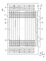
- FIG. 3 is a plan view showing a configuration example of the fingerprint detection device according to the first embodiment.
- FIG. 4 is a block diagram showing a configuration example of the fingerprint detection device.
- FIG. 5 is a cross-sectional view showing a configuration example of the display panel.
- FIG. 6 is a plan view showing a configuration example of the sensor unit according to the first embodiment.
- FIG. 7 is a plan view showing a configuration example of the drive electrode according to the first embodiment.
- FIG. 8 is a plan view showing the drive electrode and the detection electrode according to the first embodiment.
- FIG. 1 is a plan view showing a display device according to the first embodiment.
- FIG. 2 is a cross-sectional view of the display device shown in FIG. 1 cut along the lines A11-A12.
- FIG. 3 is a
- FIG. 9 is a diagram in which the electrode portion and the detection electrode are not shown in FIG.
- FIG. 10 is a plan view showing a configuration example of the electrode portion.
- FIG. 11 is a cross-sectional view showing a configuration example of the sensor unit.
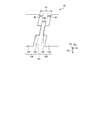
- FIG. 12 is a plan view for explaining the slit of FIG. 7.
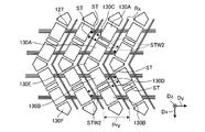
- FIG. 13 is a plan view showing the sensor unit according to the first modification of the first embodiment.
- FIG. 14 is a plan view showing the sensor unit according to the second modification of the first embodiment.
- FIG. 15 is a plan view showing the sensor unit according to the second embodiment.
- FIG. 16 is a plan view showing a sensor unit according to the first modification of the second embodiment.
- FIG. 17 is a plan view showing the sensor unit according to the second modification of the second embodiment.
- FIG. 18 is a plan view showing the sensor unit according to the third embodiment.
- FIG. 1 is a plan view showing a display device according to the first embodiment.
- FIG. 2 is a cross-sectional view of the display device shown in FIG. 1 cut along the lines A11-A12.
- the display device 1 shown in FIG. 1 is a display device having a fingerprint detection function, and is provided outside the display area AA for displaying an image, the fingerprint detection area FA, the display area AA, and the fingerprint detection area FA. It has a frame area GA.
- the fingerprint detection area FA is an area for detecting unevenness on the surface of a finger or the like that is in contact with or is close to the cover member 80.
- the display area AA and the fingerprint detection area FA are coincident or substantially the same, and it is possible to detect the fingerprint on the entire surface of the display area AA.
- the shapes of the display area AA and the fingerprint detection area FA are, for example, rectangular.
- the display device 1 of the present embodiment includes a display panel 30 and a fingerprint detection device 100.
- the fingerprint detection device 100 includes a sensor unit 10 and a cover member 80.
- the cover member 80 is a plate-shaped member having a first surface 80a and a second surface 80b opposite to the first surface 80a.
- the first surface 80a of the cover member 80 is a detection surface for detecting unevenness on the surface of a finger or the like that is in contact with or adjacent to the cover member 80, and is a display surface for the observer to visually recognize the image of the display panel 30.
- the sensor unit 10 and the display panel 30 are provided on the second surface 80b side of the cover member 80.
- the cover member 80 is a member for protecting the sensor unit 10 and the display panel 30, and covers the sensor unit 10 and the display panel 30.
- the cover member 80 is, for example, a glass substrate or a resin substrate.
- the cover member 80, the sensor unit 10, and the display panel 30 are not limited to having a rectangular shape in a plan view, but have a circular shape, an oval shape, or a different shape in which a part of these external shapes is omitted. It may be. Further, the cover member 80 is not limited to a flat plate shape. For example, when the display area AA and the fingerprint detection area FA are composed of a curved surface, or the frame area GA is composed of a curved surface curved toward the display panel 30, the cover member 80 may have a curved surface. In this case, the display device becomes a curved display having a fingerprint detection function, and fingerprints can be detected even on the curved surface of the curved display.
- the “planar view” refers to a case of being viewed from a direction perpendicular to one surface 101a of the substrate 101 shown in FIG. 3 described later.
- the direction perpendicular to one surface 101a is the "normal direction Dz of the substrate 101".
- the decorative layer 81 is provided on the second surface 80b of the cover member 80.
- the decorative layer 81 is a colored layer having a smaller light transmittance than the cover member 80.
- the decorative layer 81 can prevent the observer from seeing the wiring, the circuit, and the like that are superposed on the frame region GA.
- the decorative layer 81 is provided on the second surface 80b, but may be provided on the first surface 80a.
- the decorative layer 81 is not limited to a single layer, and may have a configuration in which a plurality of layers are stacked.
- the sensor unit 10 is a detection unit for detecting surface irregularities such as finger fins that are in contact with or close to the first surface 80a of the cover member 80. As shown in FIG. 2, the sensor unit 10 is provided between the cover member 80 and the display panel 30. When viewed from a direction (normal direction) perpendicular to the first surface 80a, the sensor unit 10 overlaps the fingerprint detection area FA and a part of the frame area GA.
- a flexible substrate 76 is connected to the sensor unit 10 in the frame region GA.
- a detection IC (not shown) for controlling the detection operation of the sensor unit 10 is mounted on the flexible substrate 76.
- the adhesive layer 71 and the adhesive layer 72 are an adhesive or a resin having translucency, and transmit visible light.
- the display panel 30 has a pixel substrate 30A, an opposing substrate 30B, a polarizing plate 34 provided on the lower side of the pixel substrate 30A, and a polarizing plate 35 provided on the upper side of the opposing substrate 30B.
- a display IC (not shown) for controlling the display operation of the display panel 30 is connected to the pixel substrate 30A via the flexible substrate 75.
- the display panel 30 is a liquid crystal panel in which a liquid crystal display element is used as a display function layer.
- the display panel 30 is not limited to this, and may be, for example, an organic EL display panel.
- the above-mentioned detection IC and display IC may be provided on the control board outside the module. Alternatively, the detection IC may be provided on the substrate 101 (see FIGS. 3 and 11) of the sensor unit 10.
- the display IC may be provided on the first substrate 31 (see FIG. 5) of the pixel substrate 30A.
- FIG. 3 is a plan view showing a configuration example of the fingerprint detection device according to the first embodiment.
- the fingerprint detection device 100 includes a substrate 101 and a sensor unit 10 provided on one surface 101a side of the substrate 101.
- the sensor unit 10 includes a drive electrode Tx and a detection electrode Rx provided on one surface 101a side of the substrate 101.
- the substrate 101 is a glass substrate having a translucency capable of transmitting visible light.
- the substrate 101 may be a translucent resin substrate or a resin film made of a resin such as polyimide.
- the sensor unit 10 is a translucent sensor.
- the drive electrode Tx is made of a translucent conductive material such as ITO (Indium Tin Oxide).
- the drive electrodes Tx are arranged side by side in the first direction Dx.
- the drive electrode Tx extends in the second direction Dy.
- the detection electrodes Rx are arranged side by side in the second direction Dy.
- the detection electrode Rx extends in the first direction Dx. In this way, the detection electrode Rx extends in a direction intersecting the extending direction of the drive electrode Tx.
- Each detection electrode Rx is connected to a flexible substrate 75 provided on the short side side of the frame region GA of the substrate 101 via a frame wiring (not shown).
- a conductive material having translucency such as ITO is used for the drive electrode Tx.
- the drive electrode Tx and the detection electrode Rx are provided in the fingerprint detection region FA.
- Capacitance is formed at the intersection of the detection electrode Rx and the drive electrode Tx.
- the sensor unit 10 performs touch detection and fingerprint detection from the change in capacitance generated between the detection electrode Rx and the drive electrode Tx.
- the drive electrode driver 15 sequentially selects the drive electrode Tx in a time-division manner and supplies the drive signal Vs to the selected drive electrode Tx. Then, fingerprint detection is performed by outputting a detection signal Vdet according to a capacitance change due to surface irregularities of a finger or the like that is in contact with or adjacent to the detection electrode Rx.
- the drive electrode driver 15 sequentially selects and drives each drive electrode block including a plurality of drive electrode Tx to perform touch detection.
- FIG. 3 shows a case where various circuits such as a detection electrode selection circuit 14 and a drive electrode driver 15 are provided in the frame region GA of the substrate 101, but this is just an example. At least a part of the various circuits may be included in the detection IC mounted on the flexible substrate 76.
- FIG. 4 is a block diagram showing a configuration example of a fingerprint detection device including a sensor unit.
- the fingerprint detection device 100 includes a sensor unit 10, a detection control unit 11, a drive electrode driver 15, a detection electrode selection circuit 14, and a detection unit 40.
- the detection control unit 11 is a circuit that controls the detection operation of the sensor unit 10.
- the drive electrode driver 15 is a circuit that supplies a drive signal Vs for detection to the drive electrode Tx of the sensor unit 10 based on the control signal supplied from the detection control unit 11.
- the detection electrode selection circuit 14 selects the detection electrode Rx of the sensor unit 10 based on the control signal supplied from the detection control unit 11 and connects it to the detection unit 40.
- the detection unit 40 is based on the control signal supplied from the detection control unit 11 and the detection signal Vdet output from the detection electrode Rx, and the detection unit 40 is on the surface of a finger or the like that is in contact with or is close to the first surface 80a of the cover member 80. It is a circuit that detects unevenness and detects the shape of a fingerprint.
- the detection unit 40 includes a detection signal amplification unit 42, an A / D conversion unit 43, a signal processing unit 44, a coordinate extraction unit 45, a synthesis unit 46, and a detection timing control unit 47.
- the detection timing control unit 47 includes a detection signal amplification unit 42, an A / D conversion unit 43, a signal processing unit 44, a coordinate extraction unit 45, and a synthesis unit based on the control signal supplied from the detection control unit 11. It is controlled so that it operates in synchronization with 46.
- the detection signal Vdet is supplied from the sensor unit 10 to the detection signal amplification unit 42 of the detection unit 40.
- the detection signal amplification unit 42 amplifies the detection signal Vdet.
- the A / D conversion unit 43 converts the analog signal output from the detection signal amplification unit 42 into a digital signal.
- the signal processing unit 44 is a logic circuit that detects the presence or absence of finger contact or proximity to the sensor unit 10 based on the output signal of the A / D conversion unit 43.
- the signal processing unit 44 performs a process of extracting a signal (absolute value
- the signal processing unit 44 compares the absolute value
- the coordinate extraction unit 45 is a logic circuit that obtains the detected coordinates when a finger contact or proximity is detected by the signal processing unit 44.
- the coordinate extraction unit 45 outputs the detected coordinates to the synthesis unit 46.
- the synthesizing unit 46 combines the detection signal Vdet output from the sensor unit 10 to generate two-dimensional information indicating the shape of a finger in contact or in close proximity.
- the synthesis unit 46 outputs the two-dimensional information as the output Vout of the detection unit 40.
- the compositing unit 46 may generate an image based on the two-dimensional information and output the image information as an output Vout.
- the above-mentioned detection IC functions as the detection unit 40 shown in FIG.
- a part of the function of the detection unit 40 may be included in the display IC described above, or may be provided as a function of an external MPU (Micro-processing unit).
- FIG. 6 is a cross-sectional view showing a configuration example of the display panel.
- the pixel substrate 30A includes a first substrate 31, a pixel electrode 32, and a common electrode 33.
- the common electrode 33 is provided on the first substrate 31.
- a plurality of pixel electrodes 32 are provided on the upper side of the common electrode 33 via an insulating layer 38, and a plurality of pixel electrodes 32 are arranged in a matrix in a plan view.
- the pixel electrode 32 is provided corresponding to the sub-pixels constituting each pixel Pix of the display panel 30, and a pixel signal for performing a display operation is supplied.
- the common electrode 33 is supplied with a direct current display drive signal and functions as a common electrode for a plurality of pixel electrodes 32.
- the common electrode 33, the insulating layer 38, and the pixel electrode 32 are laminated in this order on the first substrate 31.
- a polarizing plate 34 is provided on the lower side of the first substrate 31 via an adhesive layer.
- a TFT Thin Film Transistor, not shown, which is a switching element for display, is arranged on the first substrate 31.
- a conductive material having translucency such as ITO is used for the pixel electrode 32 and the common electrode 33.
- the array of the plurality of pixel electrodes 32 is not only a matrix-like array arranged along the first direction and the second direction orthogonal to the first direction, but also the adjacent pixel electrodes 32 are arranged in the first direction or It is also possible to adopt a configuration in which they are arranged so as to be offset in the second direction. Further, due to the difference in size of the adjacent pixel electrodes 32, two or three plurality of pixel electrodes 32 on one side of the pixel electrode 32 with respect to one pixel electrode 32 constituting the pixel array arranged in the first direction. It is also possible to adopt a configuration in which is arranged.
- the facing substrate 30B includes a second substrate 36 and a color filter 37 formed on one surface of the second substrate 36.
- the color filter 37 faces the liquid crystal layer 6 in the direction perpendicular to the first substrate 31.
- a polarizing plate 35 is provided on the second substrate 36 via an adhesive layer.
- the color filter 37 may be arranged on the first substrate 31.
- the first substrate 31 and the second substrate 36 are, for example, a glass substrate or a resin substrate.
- a liquid crystal layer 6 is provided between the first substrate 31 and the second substrate 36.
- the liquid crystal layer 6 modulates the light passing through the electric field according to the state of the electric field.
- an IPS In-Plane Switching: inplane switching
- FFS Frringe Field Switching
- An alignment film may be arranged between the liquid crystal layer 6 and the pixel substrate 30A shown in FIG. 8 and between the liquid crystal layer 6 and the facing substrate 30B, respectively.
- a lighting unit (backlight) (not shown) is provided below the first substrate 31.
- the lighting unit has a light source such as an LED, and emits light from the light source toward the first substrate 31.
- the light from the illumination unit passes through the pixel substrate 30A, and is switched between a portion where the light is blocked and not emitted and a portion where the light is emitted depending on the state of the liquid crystal at that position, thereby forming a display surface (first surface 80a). The image is displayed.
- the display panel 30 is attached to the sensor unit 10 via an adhesive layer 72 provided on the polarizing plate 35 in the display area AA.
- the sensor unit 10 is arranged at a position closer to the cover member 80 than the display panel 30 in the direction perpendicular to the second surface 80b of the cover member 80. Since the sensor unit 10 is provided on the cover member 80 side in this way, for example, as compared with the case where the detection electrode for fingerprint detection is provided integrally with the display panel 30, the detection electrode Rx and the detection surface are the first. The distance from one surface 80a can be reduced. Therefore, according to the display device 1 of the present embodiment, the detection performance can be improved.
- FIG. 6 is a plan view showing a configuration example of a detection electrode of the sensor unit according to the first embodiment.
- the detection electrode Rx intersects the plurality of drive electrodes Tx.
- the shape of the detection electrode Rx when viewed from the normal direction Dz is a zigzag line.
- the detection electrode Rx extends in the first direction Dx in a zigzag manner.
- the detection electrode Rx has a plurality of first straight line portions RxL1, a plurality of second straight line portions RxL2, and a plurality of bent portions RxB.
- the second straight line portion RxL2 extends in a direction intersecting with the first straight line portion RxL1.
- the bent portion RxB connects the first straight portion RxL1 and the second straight portion RxL2.
- the first straight line portion RxL1 extends in a direction intersecting the first direction Dx and the second direction Dy.
- the second straight line portion RxL2 also extends in a direction intersecting the first direction Dx and the second direction Dy.
- the first straight line portion RxL1 and the second straight line portion RxL2 are arranged symmetrically with respect to a virtual line (not shown) parallel to the first direction Dx.
- the arrangement interval of the bent portion RxB in the first direction Dx is Prx. Further, the arrangement interval of the bent portion RxB in the second direction Dy between the adjacent detection electrodes Rx is set to Pry. In this embodiment, for example, Pri ⁇ Prx.
- the arrangement interval of the drive electrodes Tx in the first direction Dx is Pt.
- the arrangement interval (the length of the pixel electrode 32 in the first direction Dx) in the first direction Dx is set to Ppix.
- the arrangement interval Pt of the drive electrode Tx and the arrangement interval Ppix of the pixel electrode 32 preferably satisfy the relationship of the following formula (1).
- n is an integer greater than 1.
- the sensor unit 10 can suppress the occurrence of an unintended pattern (for example, moire, a pattern reflecting light) in the fingerprint detection area FA. 0.6 ⁇ (n-1) ⁇ Ppix ⁇ Pt ⁇ 0.4 ⁇ n ⁇ Ppix... (1)
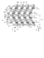
- FIG. 7 is a plan view showing a configuration example of the drive electrode according to the first embodiment.
- each of the plurality of drive electrodes Tx (for example, Tx-1, Tx-2, Tx-3, Tx-4) arranged in the first direction Dx has a plurality of electrode portions 130 and a plurality of electrode portions 130.
- Each has a connecting portion 127.
- the plurality of electrode portions 130 are arranged in the second direction Dy and are arranged apart from each other.
- the connection portion 127 connects the adjacent electrode portions of the plurality of electrode portions 130 to each other.
- one detection electrode Rx passes between the adjacent electrode portions 130 and intersects with the connection portion 127. There is.
- the longitudinal directions of the plurality of connecting portions 127 are aligned in one direction.
- the connecting portion 127 extends in the second direction.
- the other connecting portion 127 overlaps on the extension line of one connecting portion 127.
- the longitudinal directions of the connecting portions 127 of one drive electrode Tx are all in the second direction.
- the shape of the drive electrode Tx, the shape of the detection electrode Rx, and the positional relationship are aligned between the electrodes. Therefore, the capacitance of the drive electrode Tx and the capacitance of the detection electrode Rx vary. small. Further, there is an advantage that it is easy to correct the calculation of the coordinates in the sensor unit 10.
- the electrode portion 130 includes a first electrode portion 130A and a second electrode portion 130B whose shape of the electrode portion main body 131 (see FIG. 10) is different from that of the first electrode portion 130A.
- the shape of the electrode portion main body 131 of the first electrode portion 130A and the shape of the electrode portion main body 131 of the second electrode portion 130B are parallelograms, respectively.
- the shape of the electrode portion main body 131 of the first electrode portion 130A inverted upside down when viewed from the normal direction Dz is the shape of the electrode portion main body 131 of the second electrode portion 130B.
- the area of the electrode portion main body 131 of the first electrode portion 130A and the area of the electrode portion main body 131 of the second electrode portion 130B become the same.
- the drive electrodes Tx-1 and Tx-2 intersecting the first straight portion RxL1 (see FIG. 6) of the detection electrode Rx include a first electrode portion 130A having two sides parallel to the first straight portion RxL1.
- the drive electrodes Tx-3 and Tx-4 intersecting the second straight portion RxL2 (see FIG. 6) of the detection electrode Rx include a second electrode portion 130B having two sides parallel to the second straight portion RxL2.
- the electrode portion main body 131 can be arranged along the zigzag-shaped detection electrode Rx when viewed from the normal direction Dz, and the separation distance d3 between the zigzag-shaped detection electrode Rx and the electrode portion main body 131 is constant. Can be as long as.
- a dummy electrode portion 130C between the two detection electrodes Rx and between the first electrode portions 130A arranged in the first direction Dx.
- a dummy electrode portion 130D between the two detection electrodes Rx and between the second electrode portions 130B arranged in the first direction Dx.
- a dummy electrode portion 130E between the two detection electrodes Rx and between the first electrode portion 130A and the second electrode portion 130B arranged in the first direction Dx.
- a dummy electrode portion 130F between the two detection electrodes Rx and between the second electrode portion 130B and the first electrode portion 130A arranged in the first direction Dx.
- the dummy electrode portion is an electrode that is not connected to another conductive portion and is in a floating state in which the potential is not fixed.
- the shape of the dummy electrode portion 130C and the shape of the dummy electrode portion 130D are parallelograms.
- the shape of the dummy electrode portion 130C includes two sides parallel to the two sides of the first electrode portion 130A.
- the shape of the dummy electrode portion 130D includes two sides parallel to the two sides of the second electrode portion 130B.
- the shape of the dummy electrode portion 130C is the shape obtained by inverting the shape of the dummy electrode portion 130C when viewed from the normal direction Dz. As a result, the area of the dummy electrode portion 130C and the area of the dummy electrode portion 130D become the same.
- a dummy electrode portion 130E is different from the shapes of the dummy electrode portion 130C, the dummy electrode portion 130D, and the dummy electrode portion 130F.
- the shape of the dummy electrode portion 130F is 180-degree rotational symmetry of the shape of the electrode portion 130E with respect to a predetermined point.
- the dummy electrode portion 130F has the same shape as the dummy electrode portion 130E and is arranged at a position line-symmetrically with the dummy electrode portion 130F in the first direction Dx.
- the shape of the dummy electrode portion 130E and the shape of the dummy electrode portion 130F include one side parallel to one side of the first electrode portion 130A and one side parallel to one side of the second electrode portion 130B.
- the dummy electrode portions 130E lined up in the second direction Dy are located at positions sandwiching the bent portion RxB of the detection electrode Rx. As a result, the dummy electrode portion 130E and the bent portion RxB are alternately arranged in the second direction Dy.
- the dummy electrode portion 130F arranged in the second direction Dy is located at a position sandwiching the bent portion RxB of the detection electrode Rx. As a result, the dummy electrode portion 130F and the bent portion RxB are alternately arranged in the second direction Dy. As a result of forming the first electrode portion 130A, the second electrode portion 130B, the dummy electrode portion 130C, and the dummy electrode portion 130D into a parallelogram, a deformed shape other than the parallelogram formed between the bending portions RxB arranged in the second direction Dy is formed. It can be filled with the conductors of the dummy electrode portion 130E and the dummy electrode portion 130F.
- the dielectric constant between the bent portions RxB arranged in the second direction Dy can be made equal to that of the other portions, the variation in the capacitance of the drive electrode Tx for each position and the variation in the capacitance of the detection electrode Rx for each position are suppressed. Will be done.
- FIG. 8 is a plan view showing the drive electrode and the detection electrode according to the first embodiment.
- FIG. 9 is a diagram in which the electrode portion and the detection electrode are not shown in FIG.
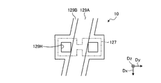
- an insulating film 129 is arranged between the connection portion 127 and the detection electrode Rx.
- the insulating film 129 is, for example, a resin insulating film.
- the insulating film 129 has a first insulating film 129A and a second insulating film 129B which is thinner than the first insulating film 129A. Further, the second insulating film 129B is provided with a contact hole 129H. As shown in FIG. 9, the connecting portion 127 is exposed at the bottom of the contact hole 129H.
- FIG. 10 is a plan view showing a configuration example of the electrode portion.
- the electrode portion 130 has an electrode portion main body 131 and a convex portion 132 in a plan view protruding from the electrode portion main body 131 toward the adjacent electrode portion 130.
- a second insulating film 129B is arranged between the convex portion 132 and the connecting portion 127.
- the convex portion 132 embeds a contact hole 129H (see FIG. 8) provided in the second insulating film 129B.
- the convex portion 132 is connected to the connecting portion 127 (see FIG. 8) via the contact hole 129H.
- the plurality of electrode portions 130 are connected to the second direction Dy via the connecting portion 127.
- the detection electrode Rx is arranged so as to overlap the convex portion 132 when viewed from the normal direction Dz, the electrode portion 130 and the detection electrode Rx are compared with the case where the electrode portion main body 131 and the detection electrode Rx overlap. The capacitance generated between them can be reduced.
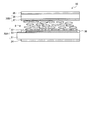
- FIG. 9 is a cross-sectional view showing a configuration example of the sensor unit.
- the cross section of the fingerprint detection region FA is a cross section obtained by cutting the plan view shown in FIG. 7 along the lines A13-A14.
- the cross section of the frame region GA is a cross section obtained by cutting a portion of the drive electrode driver 15 (see FIG. 3) including the thin film transistor Tr.
- the cross section of the fingerprint detection region FA along the A13-A14 line and the portion of the frame region GA including the thin film transistor Tr are shown.
- the cross sections are shown schematically connected.
- the sensor unit 10 has a substrate 101, a gate electrode 103 provided on the substrate 101, and a first interlayer insulating film 111 provided on the substrate 101 and covering the gate electrode 103. ..
- the gate electrode 103 is provided in the frame region GA.
- aluminum (Al), copper (Cu), silver (Ag), molybdenum (Mo) or an alloy thereof is used.
- As the material of the first interlayer insulating film 111 a silicon oxide film (SiO), a silicon nitride film (SiN), or a silicon oxide nitride film (SiON) is used.
- the first interlayer insulating film 111 is not limited to a single layer, and may be a film having a laminated structure.
- the first interlayer insulating film may be a film having a laminated structure in which a silicon nitride film is formed on a silicon oxide film.
- the sensor unit 10 has a semiconductor layer 113 formed on the first interlayer insulating film 111 and a second interlayer insulating film 121 formed on the first interlayer insulating film 111 and covering the semiconductor layer 113.
- the second interlayer insulating film 121 is provided with contact holes 121H1 and 121H2, respectively. At the bottom of the contact holes 121H1 and 121H2, the semiconductor layer 113 is exposed.
- As the material of the semiconductor layer 113 polysilicon or an oxide semiconductor is used.
- As the material of the second interlayer insulating film 121 a silicon oxide film, a silicon nitride film, or a silicon oxide nitride film is used.
- the second interlayer insulating film 121 is not limited to a single layer, and may be a film having a laminated structure.
- the second interlayer insulating film 121 may be a film having a laminated structure in which a silicon nitride film is formed on a silicon oxide film.
- the sensor unit 10 has a source electrode 123 provided on the second interlayer insulating film 121, a drain electrode 125, and a connection unit 127.
- the source electrode 123 embeds the contact hole 121H1.
- the drain electrode 125 embeds the contact hole 121H2.
- the source electrode 123 is connected to the semiconductor layer 113 via the contact hole 121H1.
- the drain electrode 125 is connected to the semiconductor layer 113 via the contact hole 121H2.
- titanium aluminum (TiAl) which is an alloy of titanium and aluminum
- the gate electrode 103, the semiconductor layer 113, the source electrode 123, and the drain electrode 125 described above are provided in the frame region GA.
- the gate electrode 103, the semiconductor layer 113, the source electrode 123, and the drain electrode 125 constitute a thin film transistor Tr in the frame region GA.
- An insulating film 129 is provided on the second interlayer insulating film 121.
- the insulating film 129 has a first insulating film 129A and a second insulating film 129B which is thinner than the first insulating film 129A.
- the first insulating film 129A provided in the frame region GA covers the source electrode 123 and the drain electrode 125. Further, a contact hole 129H is provided in the first insulating film 129A provided in the frame region GA.
- the first insulating film 129A provided in the fingerprint detection region FA covers a portion of the connection portion 127 located directly below the detection electrode Rx.
- the second insulating film 129B provided in the fingerprint detection region FA covers a portion of the connection portion 127 located directly below the electrode portion 130.
- the second insulating film 129B is provided with the contact hole 129H.
- the electrode portion 130 is provided on the second interlayer insulating film 121.
- the peripheral portion of the electrode portion 130 (for example, the convex portion 132 shown in FIG. 10) has the contact hole 129H embedded therein.
- the electrode portion 130 is connected to the connecting portion 127 via the contact hole 129H.
- the electrode portion 130 is in contact with the second interlayer insulating film 121.
- the detection electrode Rx is provided on the first insulating film 129A.
- the first insulating film 129A insulates between the detection electrode Rx and the drive electrode Tx.
- the detection electrode Rx has, for example, a first metal layer 141, a second metal layer 142, and a third metal layer 143.
- the second metal layer 142 is provided on the third metal layer 143, and the first metal layer 141 is provided on the second metal layer 142.
- molybdenum or a molybdenum alloy is used as the material of the first metal layer 141 and the third metal layer 143.
- Aluminum or an aluminum alloy is used as the material of the second metal layer 142.
- the molybdenum or molybdenum alloy constituting the first metal layer 141 has a lower reflectance of visible light than the aluminum or aluminum alloy constituting the second metal layer 142.
- the insulating film 150 is provided on the insulating film 129, the electrode portion 130, and the detection electrode Rx. The upper surface and side surfaces of the detection electrode Rx are covered with the insulating film 150.
- a film having a high refractive index and a low reflectance such as a silicon nitride film, is used.
- the insulating film 150 may be a light-shielding resin film (for example, a black resin film).
- the sensor unit 10 includes a plurality of drive electrodes Tx provided on one surface 101a side of the substrate 101 and a plurality of detection electrodes Rx provided on one surface 101a side. , Equipped with.
- the plurality of drive electrodes Tx are arranged side by side in the first direction Dx.
- the plurality of detection electrodes Rx are arranged side by side in the second direction Dy orthogonal to the first direction Dx.
- the shape of the detection electrode Rx when viewed from the normal direction Dz is a zigzag line.
- the detection electrode Rx extends in the first direction Dx in a zigzag manner.
- the detection electrode Rx has a plurality of first straight line portions RxL1, a plurality of second straight line portions RxL2, and a plurality of bent portions RxB.
- the second straight line portion RxL2 extends in a direction intersecting with the first straight line portion RxL1.
- the bent portion RxB connects the first straight portion RxL1 and the second straight portion RxL2.
- the drive electrode Tx has a plurality of electrode portions 130 arranged apart from each other, and a connecting portion 127 for connecting adjacent electrode portions among the plurality of electrode portions 130. Seen from the normal direction Dz of the substrate 101, the detection electrode Rx passes between the adjacent electrode portions 130 and intersects with the connection portion 127. According to this, the electrode portion 130 of the drive electrode Tx can be arranged along the detection electrode Rx.
- the plurality of electrode portions 130 include a first electrode portion 130A and a second electrode portion 130B having a shape different from that of the first electrode portion 130A when viewed from the normal direction Dz.
- the first electrode portion 130A can be arranged along the first straight line portion RxL1 and the second electrode portion 130B can be arranged along the second straight line portion RxL2.
- the separation distance d3 between the electrode portion main body 131 and the detection electrode Rx can be set to a constant length.
- the sensor unit 10 can suppress variations in the capacitance of the detection electrode Rx due to the separation distance d3.
- the drive electrode Tx has a dummy electrode portion 130C which is arranged between the two detection electrodes Rx and is arranged between the two first electrode portions 130A arranged in the first direction Dx and is in a floating state. ing. Further, the drive electrode Tx has a dummy electrode portion 130D which is arranged between the two detection electrodes Rx and is arranged between the two second electrode portions 130B arranged in the first direction Dx and is in a floating state. ing. As a result, the space between the two first electrode portions 130A and the space between the two second electrode portions 130B are invisible, and the occurrence of an unintended pattern can be suppressed.
- the distance between the slits ST shown in FIG. 7 is smaller than the arrangement interval Pt of the drive electrodes Tx in the first direction Dx, and the pixel electrode 32
- the slit ST is made invisible in relation to the arrangement interval Ppix, and the occurrence of an unintended pattern can be suppressed.
- the shape of the first electrode portion 130A in a plan view is a parallelogram.
- the two first electrode portions 130A arranged in the first direction Dx have a shape including two parallel sides, and the side of the dummy electrode portion 130C on the first electrode portion 130A side is the side of the first electrode portion 130A. Is parallel to.
- the areas of the two first electrode portions 130A can be easily made the same.
- the capacities of the drive electrodes Tx arranged in the first direction Dx are aligned, and the detection accuracy is improved.
- the shape of the second electrode portion 130B in a plan view is a parallelogram different in shape from the first electrode portion 130A.
- the two second electrode portions 130B arranged in the first direction Dx have a shape including two parallel sides, and the side of the dummy electrode portion 130D on the second electrode portion 130B side is the side of the second electrode portion 130B. Is parallel to.
- the areas of the two second electrode portions 130B can be easily made the same.
- the capacities of the drive electrodes Tx arranged in the first direction Dx are aligned, and the detection accuracy is improved.
- FIG. 12 is a plan view for explaining the slit of FIG. 7.
- the two slits ST may be continuous across the detection electrode Rx. If the three slits ST are continuous across the two detection electrodes Rx, the slits ST may be visualized. Therefore, in the first embodiment, the center line between the side of the first electrode portion 130A and the side of the dummy electrode portion 130C facing the first electrode portion 130A is extended along the side of the first electrode portion 130A to be the center.
- the maximum width STW1 until the line reaches the first electrode portion 130A is larger than 1 times and smaller than 3 times the arrangement interval of the two bent portions RxB in the second direction Dy.
- the center line between the side of the first electrode portion 130A and the side of the dummy electrode portion 130C facing the first electrode portion 130A is extended along the side of the first electrode portion 130A, and the center line is the first electrode.
- the maximum width STW1 until reaching the portion 130A is larger than 1 times and smaller than 3 times the arrangement interval of the two bent portions RxB in the second direction Dy.
- the three slits ST are not continuous across the two detection electrodes Rx. As a result, the slit ST is made invisible, and the occurrence of an unintended pattern can be suppressed.
- the center line between the side of the first electrode portion 130A and the side of the dummy electrode portion 130C facing the first electrode portion 130A is extended along the side of the first electrode portion 130A, and the center line is the dummy electrode portion.
- the width between the dummy electrode portions 130C where the center line reaches may be set to the maximum width STW1.
- the center line between the side of the first electrode portion 130A and the side of the dummy electrode portion 130C facing the first electrode portion 130A is extended along the side of the first electrode portion 130A, and the above-mentioned center line and the detection electrode Rx
- the first angle ⁇ 1 formed by the joint is 90 degrees, it is possible to suppress the occurrence of unintended patterns such as moire. Therefore, it is preferable that the first angle ⁇ 1 is 90 degrees.
- the center line between the side of the second electrode portion 130B and the side of the dummy electrode portion 130D facing the second electrode portion 130B is extended along the side of the second electrode portion 130B to match the above-mentioned center line.
- the first angle ⁇ 1 formed by the detection electrode Rx is also preferably 90 degrees.
- the sensor unit 10 has a first insulating film 129A arranged between the connecting portion 127 and the detection electrode Rx, and a second insulating film 129B arranged between the connecting portion 127 and the electrode portion 130. Further prepare.
- the second insulating film 129B is thinner than the first insulating film 129A. According to this, the step of the electrode portion 130 can be made smaller in the sensor portion 10 as compared with the case where the electrode portion 130 is arranged on the first insulating film 129A. As a result, the sensor unit 10 can reduce the possibility of disconnection in the electrode unit 130. Further, since the first insulating film 129A arranged between the connecting portion 127 and the detection electrode Rx is thicker than the second insulating film 129B, the capacitance of the detection electrode Rx can be reduced.
- the electrode portion 130 is a translucent electrode, and the detection electrode Rx is a thin metal wire. This makes it possible to reduce the resistance and capacitance of the detection electrode Rx. Further, since the detection electrode Rx is a thin metal wire, the electrode width is small. As a result, the area covered by the detection electrode Rx can be reduced. Therefore, the sensor unit 10 can increase the opening of the fingerprint detection area FA, and can improve the translucency of the fingerprint detection area FA.
- the ratio of the arrangement interval Prx of the bent portion RxB to the arrangement interval Pt of the drive electrode Tx is preferably 2 or less.
- FIG. 13 is a plan view showing the sensor unit according to the first modification of the first embodiment.
- the same components as those described in the first embodiment are designated by the same reference numerals, and duplicate description will be omitted.
- the two slits ST straddle the detection electrode Rx and are not continuous.
- the center line between the side of the first electrode portion 130A and the side of the dummy electrode portion 130C facing the first electrode portion 130A is extended along the side of the first electrode portion 130A.
- the maximum width STW2 until the center line reaches the first electrode portion 130A is larger than 1 times and smaller than 2 times the arrangement interval of the two bent portions RxB in the second direction Dy.
- the center line between the side of the second electrode portion 130B and the side of the dummy electrode portion 130D facing the second electrode portion 130B is extended along the side of the second electrode portion 130B, and the center line is the second electrode.
- the maximum width STW2 until reaching the portion 130B is larger than 1 times and less than 2 times the arrangement interval Pry of the two bent portions in the second direction Dy. As a result, the slit ST is made invisible, and the occurrence of an unintended pattern can be suppressed.
- FIG. 14 is a plan view showing the sensor unit according to the second modification of the first embodiment.
- the same components as those described in the first embodiment are designated by the same reference numerals, and duplicate description will be omitted.
- the connection portion 127A and the connection portion 127B have the same laminated structure as the connection portion 127 described above, but the connection positions with the electrode portion 130 in a plan view are different.
- connection portion 127A and the connection portion 127B are alternately arranged on one side and the other side with a virtual line Lcent parallel to the second direction Dy and passing through the area center of gravity AG of the electrode portion 130. It is preferable that they are arranged.
- the connection portions 127 which have lower light transmittance than the electrode portion 130, do not line up in a straight line, so that the sensor portion 10 can suppress the occurrence of unintended patterns such as moire.
- FIG. 15 is a plan view showing the sensor unit according to the second embodiment.
- the same components as those described in the first embodiment are designated by the same reference numerals, and duplicate description will be omitted.
- the dummy electrode portion 130C, the dummy electrode portion 130D, the dummy electrode portion 130E, and the dummy electrode portion 130F, which are in the first embodiment, are not provided.
- the width STW3 of extending the center lines of the sides of the first electrode portions 130A facing each other along the sides of the first electrode portion 130A until the center line reaches the first electrode portion 130A. Is greater than 1 times and less than 2 times the arrangement interval Pry of the two bent portions in the second direction Dy.
- the width STW3 from extending the center lines of the sides of the second electrode portions 130B facing each other along the sides of the second electrode portions 130B until the center lines reach the second electrode portions 130B is in the second direction.
- the distance between the two bent portions in Dy is greater than 1 times and less than 2 times the distance Pry.
- the two slits ST are not continuous across one detection electrode Rx. As a result, the sensor unit 10 can suppress the occurrence of unintended patterns such as moire.
- the center line of the sides of the first electrode portion 130A facing each other is extended along the side of the first electrode portion 130A, and the second angle ⁇ 2 formed by the above-mentioned center line and the detection electrode Rx is 90 degrees. , Moire and other unintended patterns can be suppressed. Therefore, it is preferable that the second angle ⁇ 2 is 90 degrees.
- the center line of the sides of the second electrode portions 130B facing each other is extended along the side of the second electrode portion 130B, and the second angle ⁇ 2 formed by the above-mentioned center line and the detection electrode Rx is also preferably 90 degrees.
- the slit SW has the maximum width of connecting the detection electrodes, it is larger than 1 times and smaller than 3 times the arrangement interval Pry of the two bent portions in the second direction Dy. As a result, the sensor unit 10 can suppress the occurrence of unintended patterns such as moire.
- FIG. 16 is a plan view showing a sensor unit according to the first modification of the second embodiment.
- the same components as those described in the first embodiment are designated by the same reference numerals, and duplicate description will be omitted.
- the dummy electrode portion 130C, the dummy electrode portion 130D, the dummy electrode portion 130E, and the dummy electrode portion 130F, which are in the first embodiment are not provided.
- connection portion 127A and the connection portion 127B are alternately arranged on one side and the other side with a virtual line Lcent parallel to the second direction Dy and passing through the area center of gravity AG of the electrode portion 130. It is preferable that they are arranged.
- the connection portions 127 which have lower light transmittance than the electrode portion 130, do not line up in a straight line, so that the sensor portion 10 can suppress the occurrence of unintended patterns such as moire.
- the center lines of the sides of the first electrode portions 130A facing each other are extended along the sides of the first electrode portion 130A until the center line reaches the connection portion 127A or the connection portion 127B.
- the width STW4 is larger than 1 times and less than 2 times the arrangement interval Pri of the two bent portions in the second direction Dy. Further, the width STW4 until the center line of the side of the second electrode portion 130B facing each other is extended along the side of the second electrode portion 130B and the center line reaches the connection portion 127A or the connection portion 127B is the first.
- the arrangement interval between the two bent portions in the two-way Dy is larger than 1 times and smaller than 2 times the Pri.
- the shape of the third electrode portion 130G is different from the shapes of the first electrode portion 130A and the second electrode portion 130B.
- the shape of the third electrode portion 130G includes one side parallel to one side of the first electrode portion 130A and one side parallel to one side of the second electrode portion 130B.
- the third electrode portion 130G arranged in the second direction Dy is located at a position sandwiching the bent portion RxB of the detection electrode Rx. As a result, the third electrode portion 130G and the bent portion RxB are alternately arranged in the second direction Dy.
- FIG. 17 is a plan view showing the sensor unit according to the second modification of the second embodiment.
- the same components as those described in the above-described first and second embodiments and their modified examples are designated by the same reference numerals, and duplicate description will be omitted.
- the dummy electrode portion 130C, the dummy electrode portion 130D, the dummy electrode portion 130E, and the dummy electrode portion 130F, which are in the first embodiment are not provided.
- the connection portion 127C and the connection portion 127D have the same laminated structure as the connection portion 127 described above, but the connection position and the extending direction with the electrode portion 130 in a plan view are different.
- connection portion 127C extends in the direction along the side of the first electrode portion 130A.
- the connecting portion 127D extends in a direction along the side of the second electrode portion 130B.
- the direction in which the connecting portion 127C extends and the direction in which the connecting portion 127D extends are different. Neither the direction in which the connecting portion 127C extends and the direction in which the connecting portion 127D extends is parallel to the first direction Dx and the second direction Dy.
- the connecting portion 127 which has a lower light transmittance than the electrode portion 130, does not line up in a straight line in the first direction Dx and the second direction Dy, so that the sensor unit 10 causes an unintended pattern such as moire to occur. It can be suppressed.
- the width STW5 of extending the center lines of the sides of the first electrode portions 130A facing each other along the sides of the first electrode portion 130A until the center line reaches the first electrode portion 130A. Is greater than 1 times and less than 2 times the arrangement interval Pry of the two bent portions in the second direction Dy. Further, the width STW5 from extending the center lines of the sides of the second electrode portions 130B facing each other along the sides of the second electrode portions 130B until the center lines reach the second electrode portions 130B is in the second direction.
- the distance between the two bent portions in Dy is greater than 1 times and less than 2 times the distance Pry.
- FIG. 18 is a plan view showing the sensor unit according to the third embodiment.
- the drive electrode driver 15 and the drive electrode Tx are arranged in the second direction Dy where the drive electrode Tx extends.
- the plurality of detection electrode selection circuits 14 are arranged so as to sandwich the plurality of drive electrodes Tx in the first direction Dx.
- the plurality of drive electrodes Tx described above are arranged side by side in the second direction Dy.
- the plurality of detection electrodes Rx are arranged side by side in the first direction Dx orthogonal to the second direction Dy. If the first direction Dx and the second direction Dy of the first embodiment or the second embodiment are interchanged and described, the third embodiment can be described, and thus the detailed description of the sensor unit 10 will be omitted.
- the drive electrode driver 15 includes a shift register circuit 151 and a buffer circuit 152.
- the shift register circuit 151 sequentially selects the drive electrode Tx in a time-division manner.
- the buffer circuit 152 amplifies and supplies the drive signal Vs to the selected drive electrode Tx.
- the plurality of feeder lines PL supply power to the buffer circuit 152 from the outside.
- the feeder line PL supplies power to, for example, both ends and the central portion of the second direction Dy. As a result, the power can be supplied directly from the outside of the drive electrode driver 15 without supplying power from above, so that the load during the power supply is suppressed.
- a transmissive liquid crystal display device capable of color display is shown as the display device 1, but the present invention is not limited to the transmissive liquid crystal display device compatible with color display, and the transmissive liquid crystal display compatible with monochrome display. It may be a device. Appropriate changes made without departing from the spirit of the present invention naturally belong to the technical scope of the present invention.
- the fingerprint detection device and the display device of this aspect can take the following aspects.
- a plurality of drive electrodes provided on one surface side of the substrate and arranged side by side in the first direction A plurality of zigzag-shaped detection electrodes provided on one surface side and arranged side by side in a second direction intersecting with the first direction are provided.
- the detection electrode is Multiple first straight lines and A plurality of second straight line portions extending in a direction intersecting the first straight line portion, It has a bent portion that connects the first straight portion and the second straight portion.
- the drive electrode is In a plan view, multiple electrode parts arranged apart from each other, A connecting portion that connects adjacent electrode portions in the second direction and a connecting portion.
- a fingerprint detection device having a dummy electrode portion that is arranged between the two detection electrodes and is arranged between the two electrode portions arranged in the first direction and is in a floating state.
- the plurality of electrode portions have a shape including two parallel sides.
- the center line between the side of the electrode portion and the side of the dummy electrode portion facing the electrode portion is extended along the side of the electrode portion, and the center line is the electrode portion, the dummy electrode portion and the connecting portion.
- the center line between the side of the electrode portion and the side of the dummy electrode portion facing the electrode portion is extended along the side of the electrode portion, and the angle formed by the center line and the detection electrode is 90 degrees.
- the fingerprint detection device according to any one of (1) to (3) above.
- the detection electrode is Multiple first straight lines and A plurality of second straight line portions extending in a direction intersecting the first straight line portion, It has a bent portion that connects the first straight portion and the second straight portion.
- the drive electrode is In a plan view, it has a shape including two parallel sides, and has a plurality of electrode portions arranged apart from each other. The width from extending the center lines of the sides of the electrode portions facing each other along the sides of the electrode portions until the center lines reach either the electrode portion or the connecting portion is in the second direction.
- a fingerprint detection device that is larger than 1 times and smaller than 3 times the arrangement distance between the two bent portions.
- the fingerprint detection device according to (5) above, wherein the center lines of the sides of the electrode portions facing each other are extended along the sides of the electrode portions, and the angle formed by the center line and the detection electrode is 90 degrees. .. (7)
- the plurality of electrode portions The first electrode part and The fingerprint detection device according to any one of (1) to (6) above, which includes a second electrode portion having a shape different from that of the first electrode portion in a plan view.
- the shape of the first electrode portion in a plan view is a parallelogram having two sides parallel to the extending direction of the first straight line portion.
- the shape of the second electrode portion in a plan view is a parallelogram having two sides parallel to the extending direction of the second straight portion and having a shape different from that of the first electrode portion (7).
- the fingerprint detector according to. (9) The electrode portion is a translucent electrode and The fingerprint detection device according to any one of (1) to (8) above, wherein the detection electrode is a thin metal wire. (10) The fingerprint detection device according to any one of (1) to (9) above, wherein in the first direction, the ratio of the arrangement interval of the bent portion to the arrangement interval of the drive electrode is 2 or less. (11) Any of the above (1) to (10), the connecting portion is alternately arranged on one side and the other side with a virtual line passing through the area center of gravity of the electrode portion in the second direction. The fingerprint detection device according to one. (12) Display panel and A display device including the fingerprint detection device according to any one of (1) to (11), which is arranged so as to face the display panel.
Landscapes
- Engineering & Computer Science (AREA)
- Theoretical Computer Science (AREA)
- Physics & Mathematics (AREA)
- General Physics & Mathematics (AREA)
- General Engineering & Computer Science (AREA)
- Human Computer Interaction (AREA)
- Health & Medical Sciences (AREA)
- Multimedia (AREA)
- Life Sciences & Earth Sciences (AREA)
- General Health & Medical Sciences (AREA)
- Vascular Medicine (AREA)
- Biomedical Technology (AREA)
- Public Health (AREA)
- Heart & Thoracic Surgery (AREA)
- Medical Informatics (AREA)
- Molecular Biology (AREA)
- Surgery (AREA)
- Animal Behavior & Ethology (AREA)
- Pathology (AREA)
- Veterinary Medicine (AREA)
- Quality & Reliability (AREA)
- Biophysics (AREA)
- Measurement Of Length, Angles, Or The Like Using Electric Or Magnetic Means (AREA)
- Image Input (AREA)
- Liquid Crystal (AREA)
- Measurement Of The Respiration, Hearing Ability, Form, And Blood Characteristics Of Living Organisms (AREA)
Abstract
意図しない模様の発生を抑制することができる指紋検出装置及び表示装置を提供する。指紋検出装置は、複数の駆動電極と、複数の検出電極を有している。検出電極は、複数の第1直線部と、第1直線部と交差する方向に延びる複数の第2直線部と、第1直線部と第2直線部とを接続する屈曲部と、を有している。駆動電極は、平面視で、互いに離して配置された複数の電極部と、第2方向に隣り合う電極部同士を接続する接続部と、2つの検出電極の間であって、第1方向に並べられた2つの電極部の間に配置され、フローティング状態にあるダミー電極部と、を有している。
Description
本発明は、指紋検出装置及び表示装置に関する。
液晶パネル等を備える表示装置に指紋センサが設けられることがある。指紋センサは、指紋の凹凸に応じた容量変化を検出することで、表示装置に接触した指の指紋の形状を検出する(例えば、特許文献1)。指紋センサの検出結果は、例えば、個人認証等に用いられる。指紋センサの表面にはカバーガラスが設けられている。カバーガラスの表面に指が接触又は近接すると、指紋センサは指紋を検出することができる。
指紋検出領域の電極は、カバーガラス側から入射してくる光を反射する。表示装置の表示領域と重なる位置に指紋検出領域が配置されると、指紋検出領域の電極が光を反射することにより、指紋検出領域に意図しない模様(例えば、モアレ、光を反射した模様)が視認される可能性がある。
本発明は、意図しない模様の発生を抑制することができる指紋検出装置及び表示装置を提供することを目的とする。
第一態様に係る指紋検出装置は、基板と、前記基板の一方の面側に設けられ、第1方向に並んで配置された複数の駆動電極と、前記一方の面側に設けられ、前記第1方向と交差する第2方向に並んで配置された複数のジグザグ状の検出電極と、を備え、前記検出電極は、複数の第1直線部と、前記第1直線部と交差する方向に延びる複数の第2直線部と、前記第1直線部と前記第2直線部とを接続する屈曲部と、を有し、前記駆動電極は、平面視で、互いに離して配置された複数の電極部と、前記第2方向に隣り合う電極部同士を接続する接続部と、2つの前記検出電極の間であって、前記第1方向に並べられた2つの前記電極部の間に配置され、フローティング状態にあるダミー電極部と、を有している。
第二態様に係る指紋検出装置は、基板と、前記基板の一方の面側に設けられ、第1方向に並んで配置された複数の駆動電極と、前記一方の面側に設けられ、前記第1方向と交差する第2方向に並んで配置された複数のジグザグ状の検出電極と、を備え、前記検出電極は、複数の第1直線部と、前記第1直線部と交差する方向に延びる複数の第2直線部と、前記第1直線部と前記第2直線部とを接続する屈曲部と、を有し、前記駆動電極は、平面視で、平行な2辺を含む形状を有し、互いに離して配置された複数の電極部を有し、互いに対向する前記電極部の辺の中心線を前記電極部の辺に沿って延長して、前記中心線が前記電極部及び接続部のいずれかに到達するまでの幅は、前記第2方向における2つの前記屈曲部の配置間隔の1倍よりも大きく、3倍よりも小さい。
他の態様に係る表示装置は、表示パネルと、前記表示パネルと対向して配置される上記第一態様又は第二態様の指紋検出装置とを備える。
本発明を実施するための形態(実施形態)につき、図面を参照しつつ詳細に説明する。以下の実施形態に記載した内容により本発明が限定されるものではない。また、以下に記載した構成要素には、当業者が容易に想定できるもの、実質的に同一のものが含まれる。さらに、以下に記載した構成要素は適宜組み合わせることが可能である。なお、開示はあくまで一例にすぎず、当業者において、発明の主旨を保っての適宜変更について容易に想到し得るものについては、当然に本発明の範囲に含有されるものである。また、図面は説明をより明確にするため、実際の態様に比べ、各部の幅、厚さ、形状等について模式的に表される場合があるが、あくまで一例であって、本発明の解釈を限定するものではない。また、本明細書と各図において、既出の図に関して前述したものと同様の要素には、同一の符号を付して、詳細な説明を適宜省略することがある。
(実施形態1)
図1は、実施形態1に係る表示装置を示す平面図である。図2は、図1に示した表示装置をA11-A12線で切断した断面図である。図1に示す表示装置1は、指紋検出機能付きの表示装置であり、画像を表示させるための表示領域AAと、指紋検出領域FAと、表示領域AA及び指紋検出領域FAの外側に設けられた額縁領域GAと、を有する。指紋検出領域FAは、カバー部材80に接触又は近接する指等の表面の凹凸を検出するための領域である。本実施形態の表示装置1では、表示領域AAと指紋検出領域FAとが一致又はほぼ一致しており、表示領域AAの全面において指紋を検出することが可能となっている。表示領域AA及び指紋検出領域FAの形状は、例えば矩形である。
図1は、実施形態1に係る表示装置を示す平面図である。図2は、図1に示した表示装置をA11-A12線で切断した断面図である。図1に示す表示装置1は、指紋検出機能付きの表示装置であり、画像を表示させるための表示領域AAと、指紋検出領域FAと、表示領域AA及び指紋検出領域FAの外側に設けられた額縁領域GAと、を有する。指紋検出領域FAは、カバー部材80に接触又は近接する指等の表面の凹凸を検出するための領域である。本実施形態の表示装置1では、表示領域AAと指紋検出領域FAとが一致又はほぼ一致しており、表示領域AAの全面において指紋を検出することが可能となっている。表示領域AA及び指紋検出領域FAの形状は、例えば矩形である。
図2に示すように、本実施形態の表示装置1は、表示パネル30と、指紋検出装置100と、を備える。また、指紋検出装置100は、センサ部10と、カバー部材80と、を有する。カバー部材80は、第1面80aと、第1面80aと反対側の第2面80bとを有する板状の部材である。カバー部材80の第1面80aは、接触又は近接する指等の表面の凹凸を検出するための検出面であり、かつ、表示パネル30の画像を観察者が視認するための表示面である。カバー部材80の第2面80b側に、センサ部10及び表示パネル30が設けられる。カバー部材80はセンサ部10及び表示パネル30を保護するための部材であり、センサ部10及び表示パネル30を覆っている。カバー部材80は、例えばガラス基板、又は樹脂基板である。
なお、カバー部材80、センサ部10及び表示パネル30は、平面視で長方形状の構成に限られず、円形状、長円形状、或いは、これらの外形形状の一部を欠落させた異形状の構成であってもよい。また、カバー部材80は、平板状に限られない。例えば表示領域AA及び指紋検出領域FAが曲面で構成され、或いは額縁領域GAが表示パネル30側に湾曲する曲面で構成される場合、カバー部材80の曲面を有してもよい。この場合、表示装置は、指紋検出機能を有する曲面ディスプレイとなり、曲面ディスプレイの曲面においても指紋を検出することが可能となる。なお、「平面視」とは、後述の図3に示す基板101の一方の面101aに垂直な方向から見た場合を示す。一方の面101aに垂直な方向が、「基板101の法線方向Dz」である。
図1及び図2に示すように、額縁領域GAにおいて、カバー部材80の第2面80bに加飾層81が設けられている。加飾層81は、カバー部材80よりも光の透過率が小さい着色層である。加飾層81は、額縁領域GAに重畳して設けられる配線や回路等が観察者に視認されることを抑制することができる。図2に示す例では、加飾層81は第2面80bに設けられているが、第1面80aに設けられていてもよい。また、加飾層81は、単層に限定されず、複数の層を重ねた構成であってもよい。
センサ部10は、カバー部材80の第1面80aに接触又は近接する指Fin等の表面の凹凸を検出するための検出部である。図2に示すように、センサ部10は、カバー部材80と表示パネル30との間に設けられている。第1面80aに対して垂直な方向(法線方向)から見たときに、センサ部10は、指紋検出領域FAと、額縁領域GAの一部とに重なっている。センサ部10には、額縁領域GAにおいてフレキシブル基板76が接続されている。フレキシブル基板76には、センサ部10の検出動作を制御するための検出用IC(図示せず)が実装される。
センサ部10は、一方の面が接着層71を介してカバー部材80の第2面80bと貼り合わされ、他方の面は接着層72を介して表示パネル30の偏光板35と貼り合わされる。接着層71及び接着層72は、透光性を有する接着剤又は樹脂であり、可視光を透過させる。
表示パネル30は、画素基板30Aと、対向基板30Bと、画素基板30Aの下側に設けられた偏光板34と、対向基板30Bの上側に設けられた偏光板35とを有する。画素基板30Aにフレキシブル基板75を介して、表示パネル30の表示動作を制御するための表示用IC(図示せず)が接続されている。本実施形態において、表示パネル30は、表示機能層として液晶表示素子が用いられる液晶パネルである。これに限定されず、表示パネル30は、例えば、有機EL表示パネルであってもよい。なお、上述の検出用IC及び表示用ICは、モジュール外部の制御基板に備えられていてもよい。又は、検出用ICは、センサ部10の基板101(図3、図11参照)に備えられていてもよい。表示用ICは、画素基板30Aの第1基板31(図5参照)に備えられていてもよい。
図3は、実施形態1に係る指紋検出装置の構成例を示す平面図である。図3に示すように、指紋検出装置100は、基板101と、基板101の一方の面101a側に設けられたセンサ部10と、を備える。センサ部10は、駆動電極Txと、基板101の一方の面101a側に設けられた検出電極Rxと、を含む。基板101は、可視光を透過可能な透光性を有するガラス基板である。または、基板101は、ポリイミド等の樹脂で構成された透光性の樹脂基板又は樹脂フィルムであってもよい。センサ部10は、透光性を有するセンサである。駆動電極Txは、ITO(Indium Tin Oxide)等の透光性の導電材料で構成されている。
駆動電極Txは、第1方向Dxに並んで配置されている。駆動電極Txは、第2方向Dyに延びている。検出電極Rxは、第2方向Dyに並んで配置されている。検出電極Rxは、第1方向Dxに延びている。このように、検出電極Rxは、駆動電極Txの延在方向と交差する方向に延びている。各検出電極Rxは、額縁配線(図示せず)を介して、基板101の額縁領域GAの短辺側に設けられたフレキシブル基板75に接続される。本実施形態において、駆動電極Txには、例えばITO等の透光性を有する導電性材料が用いられる。図3に示すように、駆動電極Tx及び検出電極Rxは、指紋検出領域FAに設けられている。
検出電極Rxと駆動電極Txとの交差部分に、それぞれ静電容量が形成される。センサ部10は、検出電極Rxと駆動電極Txとの間に発生する静電容量変化からタッチ検出及び指紋検出を行う。センサ部10において、相互静電容量方式の指紋検出動作を行う際、駆動電極ドライバ15は、駆動電極Txを時分割的に順次選択し、選択された駆動電極Txに駆動信号Vsを供給する。そして、接触又は近接する指等の表面の凹凸による容量変化に応じた検出信号Vdetが検出電極Rxから出力されることにより、指紋検出が行われる。なお、駆動電極ドライバ15は、複数の駆動電極Txを含む駆動電極ブロックごとに順次選択して駆動してタッチ検出を行う。
図3では、検出電極選択回路14、駆動電極ドライバ15等の各種回路が、基板101の額縁領域GAに設けられている場合を示しているが、これはあくまで一例である。各種回路の少なくとも一部は、フレキシブル基板76に実装された検出用ICに含まれていてもよい。
次に、指紋検出装置の詳細な構成について説明する。図4は、センサ部を含む指紋検出装置の構成例を示すブロック図である。図4に示すように、指紋検出装置100は、センサ部10と、検出制御部11と、駆動電極ドライバ15と、検出電極選択回路14と、検出部40とを備える。
検出制御部11は、センサ部10の検出動作を制御する回路である。駆動電極ドライバ15は、検出制御部11から供給される制御信号に基づいて、センサ部10の駆動電極Txに検出用の駆動信号Vsを供給する回路である。検出電極選択回路14は、検出制御部11から供給される制御信号に基づいて、センサ部10の検出電極Rxを選択して、検出部40に接続する。
検出部40は、検出制御部11から供給される制御信号と、検出電極Rxから出力される検出信号Vdetとに基づいて、カバー部材80の第1面80aに接触又は近接する指等の表面の凹凸を検出して、指紋の形状を検出する回路である。検出部40は、検出信号増幅部42と、A/D変換部43と、信号処理部44と、座標抽出部45と、合成部46と、検出タイミング制御部47と、を備える。検出タイミング制御部47は、検出制御部11から供給される制御信号に基づいて、検出信号増幅部42と、A/D変換部43と、信号処理部44と、座標抽出部45と、合成部46とが同期して動作するように制御する。
検出信号Vdetは、センサ部10から検出部40の検出信号増幅部42に供給される。検出信号増幅部42は、検出信号Vdetを増幅する。A/D変換部43は、検出信号増幅部42から出力されるアナログ信号をデジタル信号に変換する。
信号処理部44は、A/D変換部43の出力信号に基づいて、センサ部10に対する指の接触又は近接の有無を検出する論理回路である。信号処理部44は、指による検出信号の差分の信号(絶対値|ΔV|)を取り出す処理を行う。信号処理部44は、絶対値|ΔV|を所定のしきい値電圧と比較し、この絶対値|ΔV|がしきい値電圧未満であれば、指が非接触状態であると判断する。一方、信号処理部44は、絶対値|ΔV|がしきい値電圧以上であれば、指が接触又は近接状態であると判断する。このようにして、検出部40は、指の接触又は近接を検出することが可能となる。
座標抽出部45は、信号処理部44において指の接触又は近接が検出されたときに、その検出座標を求める論理回路である。座標抽出部45は、検出座標を合成部46に出力する。合成部46は、センサ部10から出力される検出信号Vdetを組み合わせて、接触又は近接する指の形状を示す二次元情報を生成する。合成部46は、二次元情報を検出部40の出力Voutとして出力する。又は、合成部46は、二次元情報に基づいた画像を生成し、画像情報を出力Voutとしてもよい。
上述した検出用ICは、図4に示す検出部40として機能する。検出部40の機能の一部は、上述した表示用ICに含まれていてもよく、外部のMPU(Micro-processing unit)の機能として設けられてもよい。
図6は、表示パネルの構成例を示す断面図である。画素基板30Aは、第1基板31と、画素電極32と、共通電極33とを含む。共通電極33は、第1基板31の上に設けられる。画素電極32は、絶縁層38を介して共通電極33の上側に設けられ、平面視でマトリクス状に複数配置される。画素電極32は、表示パネル30の各画素Pixを構成する副画素に対応して設けられ、表示動作を行うための画素信号が供給される。また、共通電極33は、直流の表示用駆動信号が供給され、複数の画素電極32に対する共通電極として機能する。
本実施形態において、第1基板31に対して、共通電極33、絶縁層38、画素電極32は、この順で積層されている。第1基板31の下側には、接着層を介して偏光板34が設けられる。第1基板31には、表示用のスイッチング素子であるTFT(Thin Film Transistor、図示せず)が配置される。画素電極32及び共通電極33は、例えば、ITO等の透光性を有する導電性材料が用いられる。
なお、複数の画素電極32の配列は、第1方向及び該第1方向に直交する第2方向に沿って配列されるマトリクス状の配列のみならず、隣り合う画素電極32同士が第1方向又は第2方向にずれて配置される構成を採用することもできる。また、隣り合う画素電極32の大きさの違いから、第1方向に配列される画素列を構成する1つの画素電極32に対し、当該画素電極の一側に2又は3の複数の画素電極32が配列される構成も採用可能である。
対向基板30Bは、第2基板36と、この第2基板36の一方の面に形成されたカラーフィルタ37とを含む。カラーフィルタ37は、第1基板31と垂直な方向において、液晶層6と対向する。さらに、第2基板36の上には、接着層を介して偏光板35が設けられている。なお、カラーフィルタ37は第1基板31上に配置されてもよい。本実施形態において、第1基板31及び第2基板36は、例えば、ガラス基板又は樹脂基板である。
第1基板31と第2基板36との間に液晶層6が設けられる。液晶層6は、電界の状態に応じてそこを通過する光を変調するものであり、例えば、FFS(Fringe Field Switching:フリンジフィールドスイッチング)を含むIPS(In-Plane Switching:インプレーンスイッチング)等の横電界モードの液晶が用いられる。なお、図8に示す液晶層6と画素基板30Aとの間、及び液晶層6と対向基板30Bとの間には、それぞれ配向膜が配設されてもよい。
第1基板31の下方には、図示しない照明部(バックライト)が設けられる。照明部は、例えばLED等の光源を有しており、光源からの光を第1基板31に向けて射出する。照明部からの光は、画素基板30Aを通過して、その位置の液晶の状態により光が遮られて射出しない部分と射出する部分とが切り換えられることで、表示面(第1面80a)に画像が表示される。
図2に示したように、表示パネル30は、表示領域AAにおいて偏光板35の上に設けられた接着層72を介してセンサ部10と貼り合わされる。センサ部10は、カバー部材80の第2面80bと垂直な方向において、表示パネル30よりもカバー部材80に近い位置に配置される。このようにセンサ部10は、カバー部材80側に設けられているので、例えば、表示パネル30と一体に指紋検出用の検出電極を設けた場合に比べ、検出電極Rxと、検出面である第1面80aとの距離を小さくすることができる。したがって、本実施形態の表示装置1によれば、検出性能を向上させることができる。
図6は、実施形態1に係るセンサ部の検出電極の構成例を示す平面図である。図6に示すように、検出電極Rxは、複数の駆動電極Txと交差している。法線方向Dzから見て、検出電極Rxの形状は、ジグザグ状の線である。検出電極Rxは、ジグザグしながら第1方向Dxに延びている。例えば、検出電極Rxは、複数の第1直線部RxL1と、複数の第2直線部RxL2と、複数の屈曲部RxBと、を有する。第2直線部RxL2は、第1直線部RxL1と交差する方向に延びている。また、屈曲部RxBは、第1直線部RxL1と第2直線部RxL2とを接続している。
一例を挙げると、第1直線部RxL1は、第1方向Dx及び第2方向Dyと交差する方向に延びている。第2直線部RxL2も、第1方向Dx及び第2方向Dyと交差する方向に延びている。第1直線部RxL1と第2直線部RxL2は、第1方向Dxに平行な仮想線(図示せず)を軸に、左右対称となるように配置されている。
複数の検出電極Rxの各々において、第1方向Dxにおける屈曲部RxBの配置間隔をPrxとする。また、隣り合う検出電極Rx間において、第2方向Dyにおける屈曲部RxBの配置間隔をPryとする。本実施形態では、例えば、Pry<Prxとなっている。
また、第1方向Dxにおける駆動電極Txの配置間隔をPtとする。また、指紋検出装置100と貼り合せられる表示パネル30の画素電極32について、第1方向Dxにおける配置間隔(画素電極32の第1方向Dxにおける長さ)をPpixとする。本実施形態では、駆動電極Txの配置間隔Ptと画素電極32の配置間隔Ppixは、以下の式(1)の関係を満たすことが好ましい。式(1)において、nは1より大きい整数である。これにより、センサ部10は、指紋検出領域FAに意図しない模様(例えば、モアレ、光を反射した模様)が発生することを抑制することができる。
0.6×(n-1)×Ppix≦Pt≦0.4×n×Ppix …(1)
0.6×(n-1)×Ppix≦Pt≦0.4×n×Ppix …(1)
次に、駆動電極Txの形状について、より具体的に説明する。図7は、第1実施形態に係る駆動電極の構成例を示す平面図である。図7に示すように、第1方向Dxに並ぶ複数の駆動電極Txの各々(例えば、Tx-1、Tx-2、Tx-3、Tx-4)は、複数の電極部130と、複数の接続部127とをそれぞれ有する。複数の駆動電極Txの各々において、複数の電極部130は第2方向Dyに並んでおり、互いに離して配置されている。また、複数の駆動電極Txの各々において、接続部127は、複数の電極部130のうち隣り合う電極部同士を接続している。また、図7に示すように、基板101(図3参照)の法線方向Dzから見て、1本の検出電極Rxは、隣り合う電極部130の間を通って接続部127と交差している。
また、複数の接続部127の長手方向は、一方向に揃っている。接続部127は、第2方向に延在している。実施形態1では、1つの接続部127の延長線上に、他の接続部127が重なっている。例えば、1つの駆動電極Txが有する接続部127の長手方向は、全て第2方向となっている。これにより、検出電極Rxと交差する接続部127の形状が揃うため、駆動電極Txと接続部127との間の容量が揃いやすい。
図7に示すセンサ部10では、駆動電極Txの形状と検出電極Rxの形状、位置関係が電極間で揃っているこのため、駆動電極Txの容量のばらつきや、検出電極Rxの容量のばらつきが小さい。また、センサ部10における座標の算出の補正等も実行し易いという利点がある。
また、図7に示すように、法線方向Dzから見て、電極部130の形状は複数ある。例えば、電極部130は、第1電極部130Aと、電極部本体131(図10参照)の形状が第1電極部130Aとは異なる第2電極部130Bと、を含む。法線方向Dzから見て、第1電極部130Aの電極部本体131の形状と、第2電極部130Bの電極部本体131の形状はそれぞれ平行四辺形である。法線方向Dzから見て、第1電極部130Aの電極部本体131を上下反転させた形状が、第2電極部130Bの電極部本体131の形状となっている。これにより、第1電極部130Aの電極部本体131の面積と、第2電極部130Bの電極部本体131の面積が同じになる。
例えば、検出電極Rxの第1直線部RxL1(図6参照)と交差する駆動電極Tx-1、Tx-2は、第1直線部RxL1と平行な2辺を有する第1電極部130Aを備える。また、検出電極Rxの第2直線部RxL2(図6参照)と交差する駆動電極Tx-3、Tx-4は、第2直線部RxL2と平行な2辺を有する第2電極部130Bを備える。これにより、法線方向Dzから見て、ジグザグ状の検出電極Rxに沿って電極部本体131を配置することができ、ジグザグ状の検出電極Rxと、電極部本体131との離隔距離d3を一定の長さにすることができる。
2つの検出電極Rxの間であって、第1方向Dxに並べられた第1電極部130Aの間には、ダミー電極部130Cがある。2つの検出電極Rxの間であって、第1方向Dxに並べられた第2電極部130Bの間には、ダミー電極部130Dがある。2つの検出電極Rxの間であって、第1方向Dxに並べられた第1電極部130Aと第2電極部130Bとの間には、ダミー電極部130Eがある。2つの検出電極Rxの間であって、第1方向Dxに並べられた第2電極部130Bと第1電極部130Aとの間には、ダミー電極部130Fがある。ここで、ダミー電極部とは、他の導電部とは接続しておらず、電位が固定されていないフローティング状態にある電極のことである。
ダミー電極部130Cの形状及びダミー電極部130Dの形状は、平行四辺形である。ダミー電極部130Cの形状は、第1電極部130Aの2辺と平行な2辺を含む。ダミー電極部130Dの形状は、第2電極部130Bの2辺と平行な2辺を含む。法線方向Dzから見て、ダミー電極部130Cの形状を上下反転させた形状が、ダミー電極部130Dの形状となっている。これにより、ダミー電極部130Cの面積と、ダミー電極部130Dの面積が同じになる。
2つの検出電極Rxの間であって、第1方向Dxに並べられた第1電極部130Aと第2電極部130Bの間には、ダミー電極部130E及びダミー電極部130Fがある。ダミー電極部130Eの形状は、ダミー電極部130C、ダミー電極部130D及びダミー電極部130Fの形状とは異なる。ダミー電極部130Fの形状は、所定の点を基準として電極部130Eの形状の180度回転対称である。あるいは、ダミー電極部130Fは、ダミー電極部130Eと同形状で、第1方向Dxにおいてダミー電極部130Fと線対称に位置に配置されているとも言える。ダミー電極部130Eの形状及びダミー電極部130Fの形状は、第1電極部130Aの1辺と平行な1辺と、第2電極部130Bの1辺と平行な1辺とを含む。第2方向Dyに並ぶダミー電極部130Eは、検出電極Rxの屈曲部RxBを挟む位置にある。これにより、第2方向Dyにみて、ダミー電極部130Eと、屈曲部RxBとが交互に並ぶことになる。第2方向Dyに並ぶダミー電極部130Fは、検出電極Rxの屈曲部RxBを挟む位置にある。これにより、第2方向Dyにみて、ダミー電極部130Fと、屈曲部RxBとが交互に並ぶことになる。第1電極部130A、第2電極部130B、ダミー電極部130C及びダミー電極部130Dを平行四辺形にした結果、第2方向Dyに並ぶ屈曲部RxBの間にできる平行四辺形ではない異形状をダミー電極部130E及びダミー電極部130Fの導電体で埋めることができる。そして、第2方向Dyに並ぶ屈曲部RxBの間の誘電率が他の部分と同等とできることから、位置毎の駆動電極Txの容量のばらつきや、位置毎の検出電極Rxの容量のばらつきが抑制される。
図8は、実施形態1に係る駆動電極及び検出電極を示す平面図である。図9は、図8において、電極部と検出電極の図示を省略した図である。図8に示すように、接続部127と検出電極Rxとの間には、絶縁膜129が配置されている。絶縁膜129は、例えば、樹脂絶縁膜である。絶縁膜129は、第1絶縁膜129Aと、第1絶縁膜129Aよりも厚さが薄い第2絶縁膜129Bとを有する。また、第2絶縁膜129Bにはコンタクトホール129Hが設けられている。図9に示すように、コンタクトホール129Hの底部では、接続部127が露出している。
図10は、電極部の構成例を示す平面図である。図10に示すように、電極部130は、電極部本体131と、電極部本体131から隣り合う電極部130側に突き出た、平面視での凸部132と、を有する。凸部132と接続部127との間に第2絶縁膜129Bが配置されている。凸部132は、第2絶縁膜129Bに設けられたコンタクトホール129H(図8参照)を埋め込んでいる。これにより、凸部132はコンタクトホール129Hを介して接続部127(図8参照)に接続している。そして、複数の電極部130は、接続部127を介して、第2方向Dyに接続されている。
第2方向Dyにおいて、隣り合う電極部本体131間の距離をd1とし、隣り合う凸部132間の距離をd2としたとき、d1>d2となっている。法線方向Dzから見て、凸部132と重なるように検出電極Rxが配置されているので、電極部本体131と検出電極Rxとが重なる場合と比べて、電極部130と検出電極Rxとの間に生じる容量を小さくすることができる。
次に、センサ部の層構造について説明する。図9は、センサ部の構成例を示す断面図である。図9において、指紋検出領域FAの断面は、図7に示した平面図をA13-A14線で切断した断面である。また、図9において、額縁領域GAの断面は、駆動電極ドライバ15(図3参照)の薄膜トランジスタTrを含む部分を切断した断面である。図9では、指紋検出領域FAの層構造と額縁領域GAの層構造との関係を示すために、指紋検出領域FAのA13-A14線に沿う断面と、額縁領域GAの薄膜トランジスタTrを含む部分の断面とを、模式的に繋げて示している。
図14に示すように、センサ部10は、基板101と、基板101上に設けられたゲート電極103と、基板101上に設けられてゲート電極103を覆う第1層間絶縁膜111と、を有する。ゲート電極103は額縁領域GAに設けられている。ゲート電極103の材料としては、アルミニウム(Al)、銅(Cu)、銀(Ag)、モリブデン(Mo)又はこれらの合金が用いられる。第1層間絶縁膜111の材料としては、シリコン酸化膜(SiO)、シリコン窒化膜(SiN)又はシリコン酸化窒化膜(SiON)が用いられる。また、第1層間絶縁膜111は単層に限定されず、積層構造の膜でもよい。例えば、第1層間絶縁膜は、シリコン酸化膜上にシリコン窒化膜が形成された、積層構造の膜であってもよい。
また、センサ部10は、第1層間絶縁膜111上に形成された半導体層113と、第1層間絶縁膜111上に形成されて半導体層113を覆う第2層間絶縁膜121と、を有する。第2層間絶縁膜121にはコンタクトホール121H1、121H2がそれぞれ設けられている。コンタクトホール121H1、121H2の底部では、半導体層113が露出している。半導体層113の材料としては、ポリシリコン又は酸化物半導体が用いられる。第2層間絶縁膜121の材料としては、シリコン酸化膜、シリコン窒化膜又はシリコン酸化窒化膜が用いられる。また、第2層間絶縁膜121は単層に限定されず、積層構造の膜でもよい。例えば、第2層間絶縁膜121は、シリコン酸化膜上にシリコン窒化膜が形成された、積層構造の膜であってもよい。
また、センサ部10は、第2層間絶縁膜121上に設けられたソース電極123と、ドレイン電極125と、接続部127とを有する。ソース電極123は、コンタクトホール121H1を埋め込んでいる。ドレイン電極125は、コンタクトホール121H2を埋め込んでいる。これにより、ソース電極123は、コンタクトホール121H1を介して半導体層113に接続している。ドレイン電極125は、コンタクトホール121H2を介して半導体層113に接続している。ソース電極123と、ドレイン電極125及び接続部127の材料としては、チタンとアルミニウムとの合金である、チタンアルミニウム(TiAl)が用いられる。
上述のゲート電極103、半導体層113、ソース電極123及びドレイン電極125は、額縁領域GAに設けられている。ゲート電極103、半導体層113、ソース電極123及びドレイン電極125によって、額縁領域GAの薄膜トランジスタTrが構成されている。
第2層間絶縁膜121上に絶縁膜129が設けられている。上述したように、絶縁膜129は、第1絶縁膜129Aと、第1絶縁膜129Aよりも薄膜の第2絶縁膜129Bとを有する。額縁領域GAに設けられた第1絶縁膜129Aは、ソース電極123及びドレイン電極125を覆っている。また、額縁領域GAに設けられた第1絶縁膜129Aには、コンタクトホール129Hが設けられている。一方、指紋検出領域FAに設けられた第1絶縁膜129Aは、接続部127において、検出電極Rxの直下に位置する部位を覆っている。また、指紋検出領域FAに設けられた第2絶縁膜129Bは、接続部127において、電極部130の直下に位置する部位を覆っている。上述したように、第2絶縁膜129Bにはコンタクトホール129Hが設けられている。
さらに、第2層間絶縁膜121上に電極部130が設けられている。指紋検出領域FAにおいて、電極部130の周縁部(例えば、図10に示した凸部132)は、コンタクトホール129Hを埋め込んでいる。これにより、電極部130は、コンタクトホール129Hを介して接続部127に接続している。なお、この例では、電極部130は第2層間絶縁膜121に接している。
指紋検出領域FAにおいて、第1絶縁膜129A上に検出電極Rxが設けられている。第1絶縁膜129Aにより、検出電極Rxと駆動電極Txとの間が絶縁されている。検出電極Rxは、例えば、第1金属層141と、第2金属層142及び第3金属層143を有する。第3金属層143上に第2金属層142が設けられており、第2金属層142上に第1金属層141が設けられている。例えば、第1金属層141、第3金属層143の材料には、モリブデン又はモリブデン合金が用いられる。第2金属層142の材料には、アルミニウム又はアルミニウム合金が用いられる。第1金属層141を構成するモリブデン又はモリブデン合金は、第2金属層142を構成するアルミニウム又はアルミニウム合金よりも可視光の反射率が低い。
絶縁膜129、電極部130及び検出電極Rx上に絶縁膜150が設けられている。絶縁膜150によって、検出電極Rxの上面及び側面は覆われている。絶縁膜150には、シリコン窒化膜など、高屈折率で低反射率の膜が用いられる。または、絶縁膜150は、遮光性樹脂膜(例えば、黒色の樹脂膜)であってもよい。
以上説明したように、実施形態1に係るセンサ部10は、基板101の一方の面101a側に設けられた複数の駆動電極Txと、一方の面101a側に設けられた複数の検出電極Rxと、を備える。複数の駆動電極Txは、第1方向Dxに並んで配置されている。複数の検出電極Rxは、第1方向Dxと直交する第2方向Dyに並んで配置されている。法線方向Dzから見て、検出電極Rxの形状は、ジグザグ状の線である。検出電極Rxは、ジグザグしながら第1方向Dxに延びている。すなわち、検出電極Rxは、複数の第1直線部RxL1と、複数の第2直線部RxL2と、複数の屈曲部RxBと、を有する。第2直線部RxL2は、第1直線部RxL1と交差する方向に延びている。また、屈曲部RxBは、第1直線部RxL1と第2直線部RxL2とを接続している。
また、駆動電極Txは、互いに離して配置された複数の電極部130と、複数の電極部130のうち隣り合う電極部同士を接続する接続部127と、を有する。基板101の法線方向Dzから見て、検出電極Rxは、隣り合う電極部130の間を通って接続部127と交差している。これによれば、検出電極Rxに沿って駆動電極Txの電極部130を配置することができる。
また、複数の電極部130は、第1電極部130Aと、法線方向Dzから見て第1電極部130Aとは形状が異なる第2電極部130Bと、を含む。これによれば、第1電極部130Aを第1直線部RxL1に沿って配置すると共に、第2電極部130Bを第2直線部RxL2に沿って配置することができる。そして、電極部本体131と検出電極Rxとの離隔距離d3を一定の長さにすることができる。これにより、センサ部10は、離隔距離d3が原因で、検出電極Rxの容量がばらつくことを抑制することができる。
また、駆動電極Txは、2つの検出電極Rxの間であって、第1方向Dxに並べられた2つの第1電極部130Aの間に配置され、フローティング状態にあるダミー電極部130Cを有している。また、駆動電極Txは、2つの検出電極Rxの間であって、第1方向Dxに並べられた2つの第2電極部130Bの間に配置され、フローティング状態にあるダミー電極部130Dを有している。これにより、2つの第1電極部130Aの間及び2つの第2電極部130Bの間が不可視化され、意図しない模様の発生を抑制することができる。
言い換えると、ダミー電極部130C及びダミー電極部130Dを有することにより、第1方向Dxにおける駆動電極Txの配置間隔Ptよりも、図7に示すスリットSTの間の距離が小さくなり、画素電極32の配置間隔Ppixとの関係で、スリットSTが不可視化され、意図しない模様の発生を抑制することができる。
第1電極部130Aの平面視による形状は、平行四辺形である。第1方向Dxに並べられた2つの第1電極部130Aは、平行な2辺を含む形状であり、第1電極部130A側のダミー電極部130Cの辺は、当該第1電極部130Aの辺と平行である。これにより、2つの第1電極部130Aの面積が同じにしやすくなる。その結果、第1方向Dxに並べられた駆動電極Txの容量が揃い、検出精度が高まる。
第2電極部130Bの平面視による形状は、第1電極部130Aとは形が異なる平行四辺形である。第1方向Dxに並べられた2つの第2電極部130Bは、平行な2辺を含む形状であり、第2電極部130B側のダミー電極部130Dの辺は、当該第2電極部130Bの辺と平行である。これにより、2つの第2電極部130Bの面積が同じにしやすくなる。その結果、第1方向Dxに並べられた駆動電極Txの容量が揃い、検出精度が高まる。
図12は、図7のスリットを説明するための平面図である。図12に示すように、2つのスリットSTは、検出電極Rxを跨いで、連続することがある。3つのスリットSTが、2つの検出電極Rxを跨いで連続すると、スリットSTが可視化されてしまう可能性がある。そこで、実施形態1では、第1電極部130Aの辺と、第1電極部130Aと対向するダミー電極部130Cの辺との中心線を第1電極部130Aの辺に沿って延長して、中心線が第1電極部130Aに到達するまでの最大幅STW1は、第2方向Dyにおける2つの屈曲部RxBの配置間隔の1倍よりも大きく、3倍よりも小さい。また、第1電極部130Aの辺と、第1電極部130Aと対向するダミー電極部130Cの辺との中心線を第1電極部130Aの辺に沿って延長して、中心線が第1電極部130Aに到達するまでの最大幅STW1は、第2方向Dyにおける2つの屈曲部RxBの配置間隔の1倍よりも大きく、3倍よりも小さい。換言すれば、3つのスリットSTが、2つの検出電極Rxを跨いで連続しない。これにより、スリットSTが不可視化され、意図しない模様の発生を抑制することができる。
なお、第1電極部130Aの辺と、第1電極部130Aと対向するダミー電極部130Cの辺との中心線を第1電極部130Aの辺に沿って延長して、中心線がダミー電極部130Cに到達する場合は、中心線が到達するダミー電極部130C間の幅を最大幅STW1とすればよい。
第1電極部130Aの辺と、第1電極部130Aと対向するダミー電極部130Cの辺との中心線を第1電極部130Aの辺に沿って延長して、前述の中心線と検出電極Rxとがなす第1角度θ1が、90度であると、モアレ等の意図しない模様の発生を抑制することができる。このため、第1角度θ1が90度であることが好ましい。同様に、第2電極部130Bの辺と、第2電極部130Bと対向するダミー電極部130Dの辺との中心線を第2電極部130Bの辺に沿って延長して、前述の中心線とが検出電極Rxとがなす第1角度θ1も、90度であることが好ましい。
また、センサ部10は、接続部127と検出電極Rxとの間に配置された第1絶縁膜129Aと、接続部127と電極部130との間に配置された第2絶縁膜129Bと、をさらに備える。第2絶縁膜129Bは、第1絶縁膜129Aよりも厚さが薄い。これによれば、第1絶縁膜129A上に電極部130が配置される場合と比べて、センサ部10は、電極部130の段差を小さくすることができる。これにより、センサ部10は、電極部130に断線が生じる可能性を低減することができる。また、接続部127と検出電極Rxとの間に配置される第1絶縁膜129Aは、第2絶縁膜129Bよりも厚膜であるため、検出電極Rxの容量を小さくすることができる。
また、電極部130は透光性電極であり、検出電極Rxは金属細線である。これにより、検出電極Rxの低抵抗化、低容量化が可能である。また、検出電極Rxは金属細線であるため、電極幅が小さい。これにより、検出電極Rxで覆われる面積を小さくすることができる。このため、センサ部10は、指紋検出領域FAを高開口化することが可能であり、指紋検出領域FAの透光性を高めることができる。
また、第1方向Dxにおいて、駆動電極Txの配置間隔Ptに対する屈曲部RxBの配置間隔Prxの比は2以下であることが好ましい。これにより、センサ部10は、モアレ等の意図しない模様の発生を抑制することができる。
(変形例1)
図13は、実施形態1の変形例1に係るセンサ部を示す平面図である。なお、上述した実施形態1で説明したものと同じ構成要素には同一の符号を付して重複する説明は省略する。図13に示すように、2つのスリットSTは、検出電極Rxを跨いで、連続しない。
図13は、実施形態1の変形例1に係るセンサ部を示す平面図である。なお、上述した実施形態1で説明したものと同じ構成要素には同一の符号を付して重複する説明は省略する。図13に示すように、2つのスリットSTは、検出電極Rxを跨いで、連続しない。
実施形態1の変形例1では、第1電極部130Aの辺と、第1電極部130Aと対向するダミー電極部130Cの辺との中心線を第1電極部130Aの辺に沿って延長して、中心線が第1電極部130Aに到達するまでの最大幅STW2は、第2方向Dyにおける2つの屈曲部RxBの配置間隔の1倍よりも大きく、2倍よも小さい。また、第2電極部130Bの辺と、第2電極部130Bと対向するダミー電極部130Dの辺との中心線を第2電極部130Bの辺に沿って延長して、中心線が第2電極部130Bに到達するまでの最大幅STW2は、第2方向Dyにおける2つの屈曲部の配置間隔Pryの1倍よりも大きく、2倍よも小さい。これにより、スリットSTが不可視化され、意図しない模様の発生を抑制することができる。
(変形例2)
図14は、実施形態1の変形例2に係るセンサ部を示す平面図である。なお、上述した実施形態1で説明したものと同じ構成要素には同一の符号を付して重複する説明は省略する。接続部127Aと、接続部127Bは、上述した接続部127と同じ積層構造を有するが、平面視における電極部130との接続位置が異なる。
図14は、実施形態1の変形例2に係るセンサ部を示す平面図である。なお、上述した実施形態1で説明したものと同じ構成要素には同一の符号を付して重複する説明は省略する。接続部127Aと、接続部127Bは、上述した接続部127と同じ積層構造を有するが、平面視における電極部130との接続位置が異なる。
各駆動電極Txにおいて、接続部127Aと、接続部127Bは、第2方向Dyに平行で電極部130の面積重心AGを通る仮想線Lcentを挟んで、一方の側と他方の側とに交互に配置されていることが好ましい。これにより、電極部130と比べて光の透過率が低い接続部127が一直線状に並ばないので、センサ部10はモアレ等の意図しない模様の発生を抑制することができる。
(実施形態2)
図15は、実施形態2に係るセンサ部を示す平面図である。なお、上述した実施形態1で説明したものと同じ構成要素には同一の符号を付して重複する説明は省略する。実施形態において、実施形態1にあったダミー電極部130C、ダミー電極部130D、ダミー電極部130E及びダミー電極部130Fがない。
図15は、実施形態2に係るセンサ部を示す平面図である。なお、上述した実施形態1で説明したものと同じ構成要素には同一の符号を付して重複する説明は省略する。実施形態において、実施形態1にあったダミー電極部130C、ダミー電極部130D、ダミー電極部130E及びダミー電極部130Fがない。
図15に示すように、互いに対向する第1電極部130Aの辺の中心線を第1電極部130Aの辺に沿って延長して、中心線が第1電極部130Aに到達するまでの幅STW3は、第2方向Dyにおける2つの屈曲部の配置間隔Pryの1倍よりも大きく、2倍よりも小さい。また、互いに対向する第2電極部130Bの辺の中心線を第2電極部130Bの辺に沿って延長して、中心線が第2電極部130Bに到達するまでの幅STW3は、第2方向Dyにおける2つの屈曲部の配置間隔Pryの1倍よりも大きく、2倍よりも小さい。換言すれば、2つのスリットSTは1つの検出電極Rxを跨いで連続しない。これにより、センサ部10は、モアレ等の意図しない模様の発生を抑制することができる。
互いに対向する第1電極部130Aの辺の中心線を第1電極部130Aの辺に沿って延長して、前述の中心線と検出電極Rxとがなす第2角度θ2は、90度であると、モアレ等の意図しない模様の発生を抑制することができる。このため、第2角度θ2が90度であることが好ましい。互いに対向する第2電極部130Bの辺の中心線を第2電極部130Bの辺に沿って延長して、前述の中心線と検出電極Rxとがなす第2角度θ2も90度が好ましい。
図15に示すように、スリットSWが検出電極を挟んで繋がる最大幅であっても、第2方向Dyにおける2つの屈曲部の配置間隔Pryの1倍よりも大きく、3倍よりも小さい。これにより、センサ部10は、モアレ等の意図しない模様の発生を抑制することができる。
(実施形態2の変形例1)
図16は、実施形態2の変形例1に係るセンサ部を示す平面図である。なお、上述した実施形態1で説明したものと同じ構成要素には同一の符号を付して重複する説明は省略する。実施形態において、実施形態1にあったダミー電極部130C、ダミー電極部130D、ダミー電極部130E及びダミー電極部130Fがない。
図16は、実施形態2の変形例1に係るセンサ部を示す平面図である。なお、上述した実施形態1で説明したものと同じ構成要素には同一の符号を付して重複する説明は省略する。実施形態において、実施形態1にあったダミー電極部130C、ダミー電極部130D、ダミー電極部130E及びダミー電極部130Fがない。
各駆動電極Txにおいて、接続部127Aと、接続部127Bは、第2方向Dyに平行で電極部130の面積重心AGを通る仮想線Lcentを挟んで、一方の側と他方の側とに交互に配置されていることが好ましい。これにより、電極部130と比べて光の透過率が低い接続部127が一直線状に並ばないので、センサ部10はモアレ等の意図しない模様の発生を抑制することができる。
図16に示すように、互いに対向する第1電極部130Aの辺の中心線を第1電極部130Aの辺に沿って延長して、中心線が接続部127A又は接続部127Bに到達するまでの幅STW4は、第2方向Dyにおける2つの屈曲部の配置間隔Pryの1倍よりも大きく、2倍よりも小さい。また、互いに対向する第2電極部130Bの辺の中心線を第2電極部130Bの辺に沿って延長して、中心線が接続部127A又は接続部127Bに到達するまでの幅STW4は、第2方向Dyにおける2つの屈曲部の配置間隔Pryの1倍よりも大きく、2倍よりも小さい。これにより、センサ部10は、モアレ等の意図しない模様の発生を抑制することができる。
第3電極部130Gの形状は、第1電極部130A及び第2電極部130Bの形状とは異なる。第3電極部130Gの形状は、第1電極部130Aの1辺と平行な1辺と、第2電極部130Bの1辺と平行な1辺とを含む。第2方向Dyに並ぶ第3電極部130Gは、検出電極Rxの屈曲部RxBを挟む位置にある。これにより、第2方向Dyにみて、第3電極部130Gと、屈曲部RxBとが交互に並ぶことになる。第1電極部130A、第2電極部130Bを平行四辺形にした結果、第2方向Dyに並ぶ屈曲部RxBの間にできる平行四辺形ではない異形状を第3電極部130Gの導電体で埋めることができる。
(実施形態2の変形例2)
図17は、実施形態2の変形例2に係るセンサ部を示す平面図である。なお、上述した実施形態1、実施形態2及びそれらの変形例で説明したものと同じ構成要素には同一の符号を付して重複する説明は省略する。実施形態において、実施形態1にあったダミー電極部130C、ダミー電極部130D、ダミー電極部130E及びダミー電極部130Fがない。接続部127Cと、接続部127Dは、上述した接続部127と同じ積層構造を有するが、平面視における電極部130との接続位置及び延在する方向が異なる。
図17は、実施形態2の変形例2に係るセンサ部を示す平面図である。なお、上述した実施形態1、実施形態2及びそれらの変形例で説明したものと同じ構成要素には同一の符号を付して重複する説明は省略する。実施形態において、実施形態1にあったダミー電極部130C、ダミー電極部130D、ダミー電極部130E及びダミー電極部130Fがない。接続部127Cと、接続部127Dは、上述した接続部127と同じ積層構造を有するが、平面視における電極部130との接続位置及び延在する方向が異なる。
各駆動電極Txにおいて、接続部127Cは、第1電極部130Aの辺に沿う方向に延びる。接続部127Dは、第2電極部130Bの辺に沿う方向に延びる。接続部127Cが延びる方向と、接続部127D方向とは、異なる。接続部127Cが延びる方向及び接続部127D方向は、いずれも第1方向Dx及び第2方向Dyと平行ではない。これにより、電極部130と比べて光の透過率が低い接続部127が、第1方向Dx及び第2方向Dyに一直線状に並ばないので、センサ部10はモアレ等の意図しない模様の発生を抑制することができる。
図17に示すように、互いに対向する第1電極部130Aの辺の中心線を第1電極部130Aの辺に沿って延長して、中心線が第1電極部130Aに到達するまでの幅STW5は、第2方向Dyにおける2つの屈曲部の配置間隔Pryの1倍よりも大きく、2倍よりも小さい。また、互いに対向する第2電極部130Bの辺の中心線を第2電極部130Bの辺に沿って延長して、中心線が第2電極部130Bに到達するまでの幅STW5は、第2方向Dyにおける2つの屈曲部の配置間隔Pryの1倍よりも大きく、2倍よりも小さい。これにより、センサ部10は、モアレ等の意図しない模様の発生を抑制することができる。
(実施形態3)
図18は、実施形態3に係るセンサ部を示す平面図である。実施形態3では、駆動電極ドライバ15と駆動電極Txとは、駆動電極Txが延びる第2方向Dyに並べられている。複数の検出電極選択回路14は、第1方向Dxに、複数の駆動電極Txを挟むように、配置されている。上述した複数の駆動電極Txは、第2方向Dyに並んで配置されている。複数の検出電極Rxは、第2方向Dyと直交する第1方向Dxに並んで配置されている。実施形態1又は実施形態2の第1方向Dxと第2方向Dyとを入れ替えて説明すれば、実施形態3が説明できるので、センサ部10の詳細な説明は省略する。
図18は、実施形態3に係るセンサ部を示す平面図である。実施形態3では、駆動電極ドライバ15と駆動電極Txとは、駆動電極Txが延びる第2方向Dyに並べられている。複数の検出電極選択回路14は、第1方向Dxに、複数の駆動電極Txを挟むように、配置されている。上述した複数の駆動電極Txは、第2方向Dyに並んで配置されている。複数の検出電極Rxは、第2方向Dyと直交する第1方向Dxに並んで配置されている。実施形態1又は実施形態2の第1方向Dxと第2方向Dyとを入れ替えて説明すれば、実施形態3が説明できるので、センサ部10の詳細な説明は省略する。
駆動電極ドライバ15は、シフトレジスタ回路151と、バッファー回路152とを含む。シフトレジスタ回路151は、駆動電極Txを時分割的に順次選択する。バッファー回路152は、選択された駆動電極Txに駆動信号Vsを増幅して供給する。複数の給電線PLは、バッファー回路152への外部から給電する。給電線PLは、例えば、第2方向Dyの両端および中央部分へ給電する。これにより、上からの給電をせず、駆動電極ドライバ15の外から直接給電できるので、給電途中の負荷が抑制されている。
以上、本発明の好適な実施形態とその変形例を説明したが、本発明はこのような実施形態及び変形例に限定されるものではない。実施形態及び変形例で開示された内容はあくまで一例にすぎず、本発明の趣旨を逸脱しない範囲で種々の変更が可能である。例えば、実施形態1では、表示装置1としてカラー表示可能な透過型液晶表示装置を示したが、本発明はカラー表示対応の透過型液晶表示装置に限定されず、モノクロ表示対応の透過型液晶表示装置であってもよい。本発明の趣旨を逸脱しない範囲で行われた適宜の変更についても、当然に本発明の技術的範囲に属する。
例えば、本態様の指紋検出装置及び表示装置は、以下の態様をとることができる。
(1)
基板と、
前記基板の一方の面側に設けられ、第1方向に並んで配置された複数の駆動電極と、
前記一方の面側に設けられ、前記第1方向と交差する第2方向に並んで配置された複数のジグザグ状の検出電極と、を備え、
前記検出電極は、
複数の第1直線部と、
前記第1直線部と交差する方向に延びる複数の第2直線部と、
前記第1直線部と前記第2直線部とを接続する屈曲部と、を有し、
前記駆動電極は、
平面視で、互いに離して配置された複数の電極部と、
前記第2方向に隣り合う電極部同士を接続する接続部と、
2つの前記検出電極の間であって、第1方向に並べられた2つの前記電極部の間に配置され、フローティング状態にあるダミー電極部と、を有している、指紋検出装置。
(2)
前記複数の電極部は、平行な2辺を含む形状であり、
前記電極部に対向する前記ダミー電極部の辺は、当該電極部の辺と平行である、上記(1)に記載の指紋検出装置。
(3)
前記電極部の辺と、前記電極部に対向するダミー電極部の辺との中心線を前記電極部の辺に沿って延長して、前記中心線が前記電極部、前記ダミー電極部及び接続部のいずれかに到達するまでの幅は、前記第2方向における2つの前記屈曲部の配置間隔の1倍よりも大きく、3倍よりも小さい、上記(1)又は(2)に記載の指紋検出装置。
(4)
前記電極部の辺と、前記電極部に対向するダミー電極部の辺との中心線を前記電極部の辺に沿って延長して、前記中心線と前記検出電極とがなす角度は、90度である、上記(1)乃至(3)のいずれか1つに記載の指紋検出装置。
(5)
基板と、
前記基板の一方の面側に設けられ、第1方向に並んで配置された複数の駆動電極と、
前記一方の面側に設けられ、前記第1方向と交差する第2方向に並んで配置された複数のジグザグ状の検出電極と、を備え、
前記検出電極は、
複数の第1直線部と、
前記第1直線部と交差する方向に延びる複数の第2直線部と、
前記第1直線部と前記第2直線部とを接続する屈曲部と、を有し、
前記駆動電極は、
平面視で、平行な2辺を含む形状を有し、互いに離して配置された複数の電極部を有し、
互いに対向する前記電極部の辺の中心線を前記電極部の辺に沿って延長して、前記中心線が前記電極部及び接続部のいずれかに到達するまでの幅は、前記第2方向における2つの前記屈曲部の配置間隔の1倍よりも大きく、3倍よりも小さい
指紋検出装置。
(6)
互いに対向する電極部の辺の中心線を電極部の辺に沿って延長して、前記中心線と前記検出電極とがなす角度は、90度である、上記(5)に記載の指紋検出装置。
(7)
前記複数の電極部は、
第1電極部と、
平面視で、前記第1電極部とは形状が異なる第2電極部と、を含む、上記(1)乃至(6)のいずれか1つに記載の指紋検出装置。
(8)
前記第1電極部の平面視による形状は、前記第1直線部の延びる方向と平行な2辺を有する平行四辺形であり、
前記第2電極部の平面視による形状は、前記第2直線部の延びる方向と平行な2辺を有し、かつ前記第1電極部とは形が異なる平行四辺形である、上記(7)に記載の指紋検出装置。
(9)
前記電極部は透光性電極であり、
前記検出電極は金属細線である、上記(1)乃至(8)のいずれか1つに記載の指紋検出装置。
(10)
前記第1方向において、前記駆動電極の配置間隔に対する前記屈曲部の配置間隔の比は2以下である、上記(1)乃至(9)のいずれか1つに記載の指紋検出装置。
(11)
前記接続部は、前記第2方向に前記電極部の面積重心を通る仮想線を挟んで、一方の側と他方の側とに交互に配置されている、上記(1)乃至(10)のいずれか1つに記載の指紋検出装置。
(12)
表示パネルと、
前記表示パネルと対向して配置される、上記(1)乃至(11)のいずれか1つに記載の指紋検出装置と、を備える表示装置。
(1)
基板と、
前記基板の一方の面側に設けられ、第1方向に並んで配置された複数の駆動電極と、
前記一方の面側に設けられ、前記第1方向と交差する第2方向に並んで配置された複数のジグザグ状の検出電極と、を備え、
前記検出電極は、
複数の第1直線部と、
前記第1直線部と交差する方向に延びる複数の第2直線部と、
前記第1直線部と前記第2直線部とを接続する屈曲部と、を有し、
前記駆動電極は、
平面視で、互いに離して配置された複数の電極部と、
前記第2方向に隣り合う電極部同士を接続する接続部と、
2つの前記検出電極の間であって、第1方向に並べられた2つの前記電極部の間に配置され、フローティング状態にあるダミー電極部と、を有している、指紋検出装置。
(2)
前記複数の電極部は、平行な2辺を含む形状であり、
前記電極部に対向する前記ダミー電極部の辺は、当該電極部の辺と平行である、上記(1)に記載の指紋検出装置。
(3)
前記電極部の辺と、前記電極部に対向するダミー電極部の辺との中心線を前記電極部の辺に沿って延長して、前記中心線が前記電極部、前記ダミー電極部及び接続部のいずれかに到達するまでの幅は、前記第2方向における2つの前記屈曲部の配置間隔の1倍よりも大きく、3倍よりも小さい、上記(1)又は(2)に記載の指紋検出装置。
(4)
前記電極部の辺と、前記電極部に対向するダミー電極部の辺との中心線を前記電極部の辺に沿って延長して、前記中心線と前記検出電極とがなす角度は、90度である、上記(1)乃至(3)のいずれか1つに記載の指紋検出装置。
(5)
基板と、
前記基板の一方の面側に設けられ、第1方向に並んで配置された複数の駆動電極と、
前記一方の面側に設けられ、前記第1方向と交差する第2方向に並んで配置された複数のジグザグ状の検出電極と、を備え、
前記検出電極は、
複数の第1直線部と、
前記第1直線部と交差する方向に延びる複数の第2直線部と、
前記第1直線部と前記第2直線部とを接続する屈曲部と、を有し、
前記駆動電極は、
平面視で、平行な2辺を含む形状を有し、互いに離して配置された複数の電極部を有し、
互いに対向する前記電極部の辺の中心線を前記電極部の辺に沿って延長して、前記中心線が前記電極部及び接続部のいずれかに到達するまでの幅は、前記第2方向における2つの前記屈曲部の配置間隔の1倍よりも大きく、3倍よりも小さい
指紋検出装置。
(6)
互いに対向する電極部の辺の中心線を電極部の辺に沿って延長して、前記中心線と前記検出電極とがなす角度は、90度である、上記(5)に記載の指紋検出装置。
(7)
前記複数の電極部は、
第1電極部と、
平面視で、前記第1電極部とは形状が異なる第2電極部と、を含む、上記(1)乃至(6)のいずれか1つに記載の指紋検出装置。
(8)
前記第1電極部の平面視による形状は、前記第1直線部の延びる方向と平行な2辺を有する平行四辺形であり、
前記第2電極部の平面視による形状は、前記第2直線部の延びる方向と平行な2辺を有し、かつ前記第1電極部とは形が異なる平行四辺形である、上記(7)に記載の指紋検出装置。
(9)
前記電極部は透光性電極であり、
前記検出電極は金属細線である、上記(1)乃至(8)のいずれか1つに記載の指紋検出装置。
(10)
前記第1方向において、前記駆動電極の配置間隔に対する前記屈曲部の配置間隔の比は2以下である、上記(1)乃至(9)のいずれか1つに記載の指紋検出装置。
(11)
前記接続部は、前記第2方向に前記電極部の面積重心を通る仮想線を挟んで、一方の側と他方の側とに交互に配置されている、上記(1)乃至(10)のいずれか1つに記載の指紋検出装置。
(12)
表示パネルと、
前記表示パネルと対向して配置される、上記(1)乃至(11)のいずれか1つに記載の指紋検出装置と、を備える表示装置。
1 表示装置
10 センサ部
30 表示パネル
30A 画素基板
30B 対向基板
40 検出部
71、72 接着層
75、76 フレキシブル基板
80 カバー部材
81 加飾層
100 指紋検出装置
101 基板
101a 一方の面
103 ゲート電極
111 第1層間絶縁膜
121 第2層間絶縁膜
113 半導体層
121H1、121H2、129H コンタクトホール
123 ソース電極
125 ドレイン電極
127、127A、127B、127C、127D 接続部
129 絶縁膜
129A 第1絶縁膜
129B 第2絶縁膜
130 電極部
130A 第1電極部
130B 第2電極部
130C ダミー電極部
130D ダミー電極部
130E ダミー電極部
131 電極部本体
132 凸部
141 第1金属層
142 第2金属層
143 第3金属層
150 絶縁膜
AG 面積重心
Dx 第1方向
Dy 第2方向
Dz 法線方向
FA 指紋検出領域
GA 額縁領域
Lcent 仮想線
Ppix、Prx、Pt 配置間隔
Pix 各画素
Rx 検出電極
RxB 屈曲部
RxL1 第1直線部
RxL2 第2直線部
ST スリット
Tr 薄膜トランジスタ
Tx 駆動電極
10 センサ部
30 表示パネル
30A 画素基板
30B 対向基板
40 検出部
71、72 接着層
75、76 フレキシブル基板
80 カバー部材
81 加飾層
100 指紋検出装置
101 基板
101a 一方の面
103 ゲート電極
111 第1層間絶縁膜
121 第2層間絶縁膜
113 半導体層
121H1、121H2、129H コンタクトホール
123 ソース電極
125 ドレイン電極
127、127A、127B、127C、127D 接続部
129 絶縁膜
129A 第1絶縁膜
129B 第2絶縁膜
130 電極部
130A 第1電極部
130B 第2電極部
130C ダミー電極部
130D ダミー電極部
130E ダミー電極部
131 電極部本体
132 凸部
141 第1金属層
142 第2金属層
143 第3金属層
150 絶縁膜
AG 面積重心
Dx 第1方向
Dy 第2方向
Dz 法線方向
FA 指紋検出領域
GA 額縁領域
Lcent 仮想線
Ppix、Prx、Pt 配置間隔
Pix 各画素
Rx 検出電極
RxB 屈曲部
RxL1 第1直線部
RxL2 第2直線部
ST スリット
Tr 薄膜トランジスタ
Tx 駆動電極
Claims (18)
- 基板と、
前記基板の一方の面側に設けられ、第1方向に並んで配置された複数の駆動電極と、
前記一方の面側に設けられ、前記第1方向と交差する第2方向に並んで配置された複数のジグザグ状の検出電極と、を備え、
前記検出電極は、
複数の第1直線部と、
前記第1直線部と交差する方向に延びる複数の第2直線部と、
前記第1直線部と前記第2直線部とを接続する屈曲部と、を有し、
前記駆動電極は、
平面視で、互いに離して配置された複数の電極部と、
前記第2方向に隣り合う電極部同士を接続する接続部と、
2つの前記検出電極の間であって、前記第1方向に並べられた2つの前記電極部の間に配置され、フローティング状態にあるダミー電極部と、を有している、指紋検出装置。 - 前記複数の電極部は、平行な2辺を含む形状であり、
前記電極部に対向する前記ダミー電極部の辺は、当該電極部の辺と平行である、請求項1に記載の指紋検出装置。 - 前記電極部の辺と、前記電極部に対向するダミー電極部の辺との中心線を前記電極部の辺に沿って延長して、前記中心線が前記電極部、前記ダミー電極部及び接続部のいずれかに到達するまでの幅は、前記第2方向における2つの前記屈曲部の配置間隔の1倍よりも大きく、3倍よりも小さい、請求項1に記載の指紋検出装置。
- 前記電極部の辺と、前記電極部に対向するダミー電極部の辺との中心線を前記電極部の辺に沿って延長して、前記中心線と前記検出電極とがなす角度は、90度である、請求項1に記載の指紋検出装置。
- 前記複数の電極部は、
第1電極部と、
平面視で、前記第1電極部とは形状が異なる第2電極部と、を含む、請求項1に記載の指紋検出装置。 - 前記第1電極部の平面視による形状は、前記第1直線部の延びる方向と平行な2辺を有する平行四辺形であり、
前記第2電極部の平面視による形状は、前記第2直線部の延びる方向と平行な2辺を有し、かつ前記第1電極部とは形が異なる平行四辺形である、請求項5に記載の指紋検出装置。 - 前記電極部は透光性電極であり、
前記検出電極は金属細線である、請求項1に記載の指紋検出装置。 - 前記第1方向において、前記駆動電極の配置間隔に対する前記屈曲部の配置間隔の比は2以下である、請求項1に記載の指紋検出装置。
- 前記接続部は、前記第2方向に前記電極部の面積重心を通る仮想線を挟んで、一方の側と他方の側とに交互に配置されている、請求項1に記載の指紋検出装置。
- 表示パネルと、
前記表示パネルと対向して配置される、請求項1に記載の指紋検出装置と、を備える表示装置。 - 基板と、
前記基板の一方の面側に設けられ、第1方向に並んで配置された複数の駆動電極と、
前記一方の面側に設けられ、前記第1方向と交差する第2方向に並んで配置された複数のジグザグ状の検出電極と、を備え、
前記検出電極は、
複数の第1直線部と、
前記第1直線部と交差する方向に延びる複数の第2直線部と、
前記第1直線部と前記第2直線部とを接続する屈曲部と、を有し、
前記駆動電極は、
平面視で、平行な2辺を含む形状を有し、互いに離して配置された複数の電極部を有し、
互いに対向する前記電極部の辺の中心線を前記電極部の辺に沿って延長して、前記中心線が前記電極部及び接続部のいずれかに到達するまでの幅は、前記第2方向における2つの前記屈曲部の配置間隔の1倍よりも大きく、3倍よりも小さい
指紋検出装置。 - 互いに対向する電極部の辺の中心線を電極部の辺に沿って延長して、前記中心線と前記検出電極とがなす角度は、90度である、請求項11に記載の指紋検出装置。
- 前記複数の電極部は、
第1電極部と、
平面視で、前記第1電極部とは形状が異なる第2電極部と、を含む、請求項11に記載の指紋検出装置。 - 前記第1電極部の平面視による形状は、前記第1直線部の延びる方向と平行な2辺を有する平行四辺形であり、
前記第2電極部の平面視による形状は、前記第2直線部の延びる方向と平行な2辺を有し、かつ前記第1電極部とは形が異なる平行四辺形である、請求項13に記載の指紋検出装置。 - 前記電極部は透光性電極であり、
前記検出電極は金属細線である、請求項11に記載の指紋検出装置。 - 前記第1方向において、前記駆動電極の配置間隔に対する前記屈曲部の配置間隔の比は2以下である、請求項11に記載の指紋検出装置。
- 前記接続部は、前記第2方向に前記電極部の面積重心を通る仮想線を挟んで、一方の側と他方の側とに交互に配置されている、請求項11に記載の指紋検出装置。
- 表示パネルと、
前記表示パネルと対向して配置される、請求項11に記載の指紋検出装置と、を備える表示装置。
Priority Applications (4)
| Application Number | Priority Date | Filing Date | Title |
|---|---|---|---|
| CN202080021680.9A CN113573635B (zh) | 2019-03-28 | 2020-03-10 | 指纹检测装置和显示装置 |
| DE112020000995.5T DE112020000995T5 (de) | 2019-03-28 | 2020-03-10 | Fingerabdruck-detektionsvorrichtung und anzeigevorrichtung |
| US17/482,709 US11710336B2 (en) | 2019-03-28 | 2021-09-23 | Fingerprint detection device and display device |
| US18/204,140 US20230306777A1 (en) | 2019-03-28 | 2023-05-31 | Fingerprint detection device and display device |
Applications Claiming Priority (2)
| Application Number | Priority Date | Filing Date | Title |
|---|---|---|---|
| JP2019-062440 | 2019-03-28 | ||
| JP2019062440A JP2020160380A (ja) | 2019-03-28 | 2019-03-28 | 指紋検出装置及び表示装置 |
Related Child Applications (1)
| Application Number | Title | Priority Date | Filing Date |
|---|---|---|---|
| US17/482,709 Continuation US11710336B2 (en) | 2019-03-28 | 2021-09-23 | Fingerprint detection device and display device |
Publications (1)
| Publication Number | Publication Date |
|---|---|
| WO2020195802A1 true WO2020195802A1 (ja) | 2020-10-01 |
Family
ID=72611417
Family Applications (1)
| Application Number | Title | Priority Date | Filing Date |
|---|---|---|---|
| PCT/JP2020/010370 Ceased WO2020195802A1 (ja) | 2019-03-28 | 2020-03-10 | 指紋検出装置及び表示装置 |
Country Status (5)
| Country | Link |
|---|---|
| US (2) | US11710336B2 (ja) |
| JP (1) | JP2020160380A (ja) |
| CN (1) | CN113573635B (ja) |
| DE (1) | DE112020000995T5 (ja) |
| WO (1) | WO2020195802A1 (ja) |
Families Citing this family (1)
| Publication number | Priority date | Publication date | Assignee | Title |
|---|---|---|---|---|
| WO2022053908A1 (ja) * | 2020-09-11 | 2022-03-17 | 株式会社半導体エネルギー研究所 | 表示装置、表示モジュール、及び電子機器 |
Citations (4)
| Publication number | Priority date | Publication date | Assignee | Title |
|---|---|---|---|---|
| JPH11110115A (ja) * | 1997-09-30 | 1999-04-23 | Fujitsu General Ltd | デジタイザ装置 |
| JP2015109067A (ja) * | 2013-10-22 | 2015-06-11 | パナソニックIpマネジメント株式会社 | 入力装置および表示装置 |
| JP2016004183A (ja) * | 2014-06-18 | 2016-01-12 | 株式会社ジャパンディスプレイ | 表示装置 |
| JP2018005291A (ja) * | 2016-06-27 | 2018-01-11 | 株式会社ジャパンディスプレイ | 表示装置 |
Family Cites Families (16)
| Publication number | Priority date | Publication date | Assignee | Title |
|---|---|---|---|---|
| JP4308376B2 (ja) | 1999-08-09 | 2009-08-05 | セイコーインスツル株式会社 | 指紋読み取り装置 |
| US6525547B2 (en) * | 2001-04-17 | 2003-02-25 | Sentronics Corporation | Capacitive two dimensional sensor |
| US9870111B2 (en) * | 2013-10-15 | 2018-01-16 | Sharp Kabushiki Kaisha | Touchscreen panel with driving electrodes connected to a plurality of lead lines extending in parallel to sensing electrodes |
| JP6046600B2 (ja) * | 2013-12-16 | 2016-12-21 | 株式会社ジャパンディスプレイ | タッチ検出機能付き表示装置及び電子機器 |
| JP6320227B2 (ja) * | 2014-01-17 | 2018-05-09 | 株式会社ジャパンディスプレイ | 表示装置 |
| WO2016136661A1 (ja) * | 2015-02-24 | 2016-09-01 | シャープ株式会社 | タッチセンサ付き表示装置 |
| JP2016212517A (ja) * | 2015-04-30 | 2016-12-15 | 凸版印刷株式会社 | 導電性フィルム、タッチパネル、および、表示装置 |
| WO2016208660A1 (ja) * | 2015-06-24 | 2016-12-29 | シャープ株式会社 | タッチパネル、及び表示装置 |
| JP6612075B2 (ja) * | 2015-07-23 | 2019-11-27 | 株式会社ジャパンディスプレイ | 表示装置、入力装置および表示装置の製造方法 |
| JP6603544B2 (ja) * | 2015-10-28 | 2019-11-06 | 株式会社ジャパンディスプレイ | タッチ検出装置、タッチ検出機能付き表示装置 |
| JP6539190B2 (ja) * | 2015-11-20 | 2019-07-03 | 株式会社ジャパンディスプレイ | タッチ検出装置及びタッチ検出機能付き表示装置 |
| JP2017211775A (ja) * | 2016-05-24 | 2017-11-30 | 凸版印刷株式会社 | 導電性フィルム、タッチパネル、および、表示装置 |
| KR102698761B1 (ko) * | 2016-08-02 | 2024-08-26 | 삼성디스플레이 주식회사 | 터치 패널 및 이를 포함하는 표시 장치 |
| JP7065110B2 (ja) * | 2017-09-29 | 2022-05-11 | 株式会社ジャパンディスプレイ | 指紋検出装置及び表示装置 |
| WO2019065967A1 (ja) * | 2017-09-29 | 2019-04-04 | 株式会社ジャパンディスプレイ | 指紋検出装置及び表示装置 |
| JP7281940B2 (ja) * | 2019-03-28 | 2023-05-26 | 株式会社ジャパンディスプレイ | 検出装置付き表示機器 |
-
2019
- 2019-03-28 JP JP2019062440A patent/JP2020160380A/ja active Pending
-
2020
- 2020-03-10 WO PCT/JP2020/010370 patent/WO2020195802A1/ja not_active Ceased
- 2020-03-10 DE DE112020000995.5T patent/DE112020000995T5/de active Pending
- 2020-03-10 CN CN202080021680.9A patent/CN113573635B/zh active Active
-
2021
- 2021-09-23 US US17/482,709 patent/US11710336B2/en active Active
-
2023
- 2023-05-31 US US18/204,140 patent/US20230306777A1/en not_active Abandoned
Patent Citations (4)
| Publication number | Priority date | Publication date | Assignee | Title |
|---|---|---|---|---|
| JPH11110115A (ja) * | 1997-09-30 | 1999-04-23 | Fujitsu General Ltd | デジタイザ装置 |
| JP2015109067A (ja) * | 2013-10-22 | 2015-06-11 | パナソニックIpマネジメント株式会社 | 入力装置および表示装置 |
| JP2016004183A (ja) * | 2014-06-18 | 2016-01-12 | 株式会社ジャパンディスプレイ | 表示装置 |
| JP2018005291A (ja) * | 2016-06-27 | 2018-01-11 | 株式会社ジャパンディスプレイ | 表示装置 |
Also Published As
| Publication number | Publication date |
|---|---|
| US20220012450A1 (en) | 2022-01-13 |
| US20230306777A1 (en) | 2023-09-28 |
| JP2020160380A (ja) | 2020-10-01 |
| US11710336B2 (en) | 2023-07-25 |
| CN113573635B (zh) | 2024-06-11 |
| DE112020000995T5 (de) | 2021-11-11 |
| CN113573635A (zh) | 2021-10-29 |
Similar Documents
| Publication | Publication Date | Title |
|---|---|---|
| KR102736214B1 (ko) | 전자 장치 | |
| JP7065110B2 (ja) | 指紋検出装置及び表示装置 | |
| US11194197B2 (en) | Display device | |
| US11132079B2 (en) | Sensor device and sensor-equipped display device including detection electrode | |
| US11460883B2 (en) | Display device | |
| US10522566B2 (en) | Touch display device | |
| JP7046566B2 (ja) | タッチパネル付き表示装置 | |
| CN112394827B (zh) | 触摸显示装置 | |
| US12242681B2 (en) | Display device with wires overlapping electrodes | |
| US20150355752A1 (en) | Sensor-equipped display device | |
| US11054954B2 (en) | Fingerprint detection device and display device | |
| US20230306777A1 (en) | Fingerprint detection device and display device | |
| CN109754764B (zh) | 显示装置 | |
| JP2021043419A (ja) | 表示装置 | |
| US20230019559A1 (en) | Detection device and display device |
Legal Events
| Date | Code | Title | Description |
|---|---|---|---|
| 121 | Ep: the epo has been informed by wipo that ep was designated in this application |
Ref document number: 20777835 Country of ref document: EP Kind code of ref document: A1 |
|
| 122 | Ep: pct application non-entry in european phase |
Ref document number: 20777835 Country of ref document: EP Kind code of ref document: A1 |