WO2020195759A1 - センサ付き表示装置 - Google Patents
センサ付き表示装置 Download PDFInfo
- Publication number
- WO2020195759A1 WO2020195759A1 PCT/JP2020/010121 JP2020010121W WO2020195759A1 WO 2020195759 A1 WO2020195759 A1 WO 2020195759A1 JP 2020010121 W JP2020010121 W JP 2020010121W WO 2020195759 A1 WO2020195759 A1 WO 2020195759A1
- Authority
- WO
- WIPO (PCT)
- Prior art keywords
- sensor
- display device
- signal line
- detection electrode
- pixels
- Prior art date
- Legal status (The legal status is an assumption and is not a legal conclusion. Google has not performed a legal analysis and makes no representation as to the accuracy of the status listed.)
- Ceased
Links
Images




Classifications
-
- G—PHYSICS
- G06—COMPUTING OR CALCULATING; COUNTING
- G06F—ELECTRIC DIGITAL DATA PROCESSING
- G06F3/00—Input arrangements for transferring data to be processed into a form capable of being handled by the computer; Output arrangements for transferring data from processing unit to output unit, e.g. interface arrangements
- G06F3/01—Input arrangements or combined input and output arrangements for interaction between user and computer
- G06F3/03—Arrangements for converting the position or the displacement of a member into a coded form
- G06F3/041—Digitisers, e.g. for touch screens or touch pads, characterised by the transducing means
- G06F3/0412—Digitisers structurally integrated in a display
-
- G—PHYSICS
- G02—OPTICS
- G02F—OPTICAL DEVICES OR ARRANGEMENTS FOR THE CONTROL OF LIGHT BY MODIFICATION OF THE OPTICAL PROPERTIES OF THE MEDIA OF THE ELEMENTS INVOLVED THEREIN; NON-LINEAR OPTICS; FREQUENCY-CHANGING OF LIGHT; OPTICAL LOGIC ELEMENTS; OPTICAL ANALOGUE/DIGITAL CONVERTERS
- G02F1/00—Devices or arrangements for the control of the intensity, colour, phase, polarisation or direction of light arriving from an independent light source, e.g. switching, gating or modulating; Non-linear optics
- G02F1/01—Devices or arrangements for the control of the intensity, colour, phase, polarisation or direction of light arriving from an independent light source, e.g. switching, gating or modulating; Non-linear optics for the control of the intensity, phase, polarisation or colour
- G02F1/13—Devices or arrangements for the control of the intensity, colour, phase, polarisation or direction of light arriving from an independent light source, e.g. switching, gating or modulating; Non-linear optics for the control of the intensity, phase, polarisation or colour based on liquid crystals, e.g. single liquid crystal display cells
- G02F1/133—Constructional arrangements; Operation of liquid crystal cells; Circuit arrangements
- G02F1/136—Liquid crystal cells structurally associated with a semi-conducting layer or substrate, e.g. cells forming part of an integrated circuit
- G02F1/1362—Active matrix addressed cells
- G02F1/1368—Active matrix addressed cells in which the switching element is a three-electrode device
-
- G—PHYSICS
- G06—COMPUTING OR CALCULATING; COUNTING
- G06F—ELECTRIC DIGITAL DATA PROCESSING
- G06F3/00—Input arrangements for transferring data to be processed into a form capable of being handled by the computer; Output arrangements for transferring data from processing unit to output unit, e.g. interface arrangements
- G06F3/01—Input arrangements or combined input and output arrangements for interaction between user and computer
- G06F3/03—Arrangements for converting the position or the displacement of a member into a coded form
- G06F3/041—Digitisers, e.g. for touch screens or touch pads, characterised by the transducing means
- G06F3/0416—Control or interface arrangements specially adapted for digitisers
- G06F3/04164—Connections between sensors and controllers, e.g. routing lines between electrodes and connection pads
-
- G—PHYSICS
- G06—COMPUTING OR CALCULATING; COUNTING
- G06F—ELECTRIC DIGITAL DATA PROCESSING
- G06F3/00—Input arrangements for transferring data to be processed into a form capable of being handled by the computer; Output arrangements for transferring data from processing unit to output unit, e.g. interface arrangements
- G06F3/01—Input arrangements or combined input and output arrangements for interaction between user and computer
- G06F3/03—Arrangements for converting the position or the displacement of a member into a coded form
- G06F3/041—Digitisers, e.g. for touch screens or touch pads, characterised by the transducing means
- G06F3/044—Digitisers, e.g. for touch screens or touch pads, characterised by the transducing means by capacitive means
- G06F3/0443—Digitisers, e.g. for touch screens or touch pads, characterised by the transducing means by capacitive means using a single layer of sensing electrodes
Definitions
- the present invention relates to a display device with a sensor.
- Patent Document 1 describes a display device with a built-in touch screen.
- This touch screen built-in display device has a plurality of detection electrodes and a plurality of sensor wirings.
- the plurality of sensor wires are connected to the plurality of detection electrodes.
- the sensor wiring is superimposed on the signal line for transmitting the video data signal via the insulating layer.
- the sensor wiring is covered with a detection electrode.
- An object of the present invention is to provide a display device with a sensor in which deterioration of display quality is suppressed even if sensor wiring is superimposed on slits of two adjacent detection electrodes.
- the display device with a sensor of one aspect includes a first substrate, a plurality of detection electrodes arranged in a matrix above the first substrate in a first direction and in a second direction intersecting the first direction, and said.
- a plurality of sensor wirings connected to a detection electrode, a plurality of pixels including a plurality of pixels and arranged in a matrix in the first direction and the second direction, and a switching element of the pixels are scanned, and the first
- the sensor wiring and the signal line include a plurality of scanning lines extending in one direction and a plurality of signal lines connected to the switching element of the pixel and extending in the second direction.
- the switching elements of the two pixels which are alternately arranged in the first direction and formed in the same layer and are arranged adjacent to each other in the first direction, are connected to one signal line, and the signal line is connected to the two pixels.
- the sensor wiring is between the two pixels arranged in the first direction, and the sensor wiring is superimposed on the slits of the two detection electrodes adjacent to each other in the first direction. ..
- FIG. 1 is an exploded perspective view showing a display device of this embodiment.
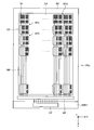
- FIG. 2 is a plan view schematically showing the array substrate.
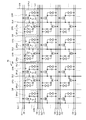
- FIG. 3 is a circuit diagram showing the pixel arrangement of the display area according to the present embodiment.
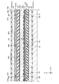
- FIG. 4 is a plan view illustrating the arrangement of sensor wiring and signal lines in a schematic plan view of pixels.
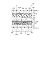
- FIG. 5 is a partial cross-sectional view illustrating the VV'cross section of FIG.
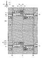
- FIG. 6 is an explanatory diagram for explaining the connection position between the sensor wiring and the detection electrode.
- FIG. 7 is a partial cross-sectional view illustrating the VII-VII'cross section of FIGS. 4 and 6.
- FIG. 8 is a partial cross-sectional view illustrating the VIII-VIII'cross section of FIG.
- FIG. 9 is a partial cross-sectional view illustrating the IX-IX'cross section of FIG.
- FIG. 1 is an exploded perspective view showing the display device of the present embodiment.
- the display device PNL with a sensor includes an array substrate SUB1 and a counter substrate SUB2.
- a peripheral area BE is provided outside the display area DA.
- the display area DA is formed in a rectangular shape, but the outer shape of the display area DA is not limited.
- the display area DA may have a notch, the display area DA may be formed in another polygonal shape, or the display area DA may be formed in another shape such as a circular shape or an elliptical shape. You may.
- the first direction X is the direction along the short side of the display area DA.
- the second direction Y is a direction that intersects (or is orthogonal to) the first direction X. Not limited to this, the second direction Y may intersect the first direction X at an angle other than 90 °.
- the plane defined by the first direction X and the second direction Y is parallel to the plane of the array substrate SUB1.
- the third direction Z orthogonal to the first direction X and the second direction Y is the thickness direction of the array substrate SUB1.
- the display area DA is an area for displaying an image, and is an area that overlaps with a plurality of pixels Pix.
- the peripheral region BE indicates a region inside the outer circumference of the array substrate SUB1 and outside the display region DA.
- the peripheral area BE may have a frame shape surrounding the display area DA, and in that case, the peripheral area BE can be said to be a frame area.
- the display area DA for displaying an image includes a sensor area included in a detection device for detecting capacitance.
- a plurality of detection electrodes CE are arranged in a matrix in the first direction X and the second direction Y in the display region DA.
- Each detection electrode CE is schematically shown in a rectangular shape or a square shape in a plan view, and the detailed shape of the detection electrode CE will be described later.
- the detection electrode CE is made of a translucent conductive material such as ITO (Indium Tin Oxide).
- an outer edge wiring CE-G and an integrated circuit CP are provided in the peripheral region BE on one surface side of the array substrate SUB1.
- the outer edge wiring CE-G is continuously provided along the long side and the short side of the display area DA, and surrounds the display area DA.
- the display device PNL with a sensor is a display device in which the sensor area is integrated with the display area DA. Specifically, in the display device PNL with a sensor, a part of the member of the display area DA is the detection electrode CE of the sensor area.
- FIG. 2 is a plan view schematically showing the array substrate.
- the detection electrode CE is divided into a matrix in the first direction X and the second direction Y by the slits SPA and SPB.
- a connection circuit MP and an integrated circuit CP are provided on the short side of the peripheral region BE.
- a flexible substrate (not shown) is connected to the short side of the peripheral region BE.
- the arrangement of the connection circuit MP and the integrated circuit CP is not limited to this, and may be provided on, for example, a control board or a flexible board outside the module.
- the detection electrode CE is electrically connected to the integrated circuit CP via the sensor wiring SM and the connection circuit MP.
- Each of the plurality of sensor wiring SMs is electrically connected to each of the plurality of detection electrodes CEs arranged in the display area DA, and is led out to the peripheral area BE.
- Each of the plurality of sensor wiring SMs extends along the second direction Y, and the plurality of sensor wiring SMs are arranged side by side in the first direction X.
- the drive circuit built in the integrated circuit CP is connected to a plurality of detection electrodes CE via the connection circuit MP arranged in the peripheral region BE and the sensor wiring SM.
- the contact hole TH has a pedestal (see FIG. 7) in which the detection electrode CE and the sensor wiring SM superimposed on the detection electrode CE are electrically connected.
- One sensor wiring SM is schematically connected to one detection electrode CE in FIG.
- the display device PNL with a sensor further includes a connection circuit MP.
- the connection circuit MP is provided between the detection electrode CE and the integrated circuit CP.
- the connection circuit MP is a circuit that switches between connection and disconnection between the detection electrode CE to be detected and driven and the integrated circuit CP based on the control signal supplied from the integrated circuit CP.
- the connection circuit MP has an analog front end.
- FIG. 3 is a circuit diagram showing the pixel arrangement of the display area according to the present embodiment.
- a plurality of scanning lines GL1, GL2, GL3, GL4, GL5 and GL6 may be collectively referred to as GL.
- the scanning line GL extends in the first direction.
- a plurality of signal lines SL1, SL2, SL3 and SL4 may be collectively referred to as a signal line SL.
- the signal line SL extends in the second direction, which intersects the first direction.
- the array substrate SUB1 is formed with switching elements Tr, signal lines SL, scanning lines GL, and the like of the sub-pixels SPix1, SPix2, and SPix3 shown in FIG.
- the signal lines SL1 to SL4 are wirings for supplying a pixel signal to each pixel electrode PE (see FIG. 4).
- the scanning lines GL1 to GL6 are wirings for supplying a gate signal for driving each switching element Tr.
- the pixel Pix of the display area DA shown in FIG. 1 includes a plurality of sub-pixels SPix1, SPix2, and SPix3 arranged in a matrix.
- the plurality of sub-pixels SPix1, SPix2, and SPix3 may be generically referred to as sub-pixel SPix.
- the sub-pixels SPix1, SPix2, and SPix3 each have the capacitance of the switching element Tr and the liquid crystal layer LC.
- the switching element Tr is composed of a thin film transistor, and in this example, it is composed of an n-channel MOS (Metal Oxide Semiconductor) type TFT.
- a third insulating layer 13 (see FIG. 5) is provided between the pixel electrode PE and the detection electrode CE, which will be described later, and the holding capacitance Cs shown in FIG. 3 is formed by these.
- color regions colored in three colors of red (R), green (G), and blue (B) are periodically arranged.
- Each of the sub-pixels SPix1, SPix2, and SPix3 shown in FIG. 3 described above is associated with three color regions of R, G, and B as a set.
- the pixel Pix is configured with the sub-pixels SPix1, SPix2, and SPix3 corresponding to the three color regions as a set.
- the color filter may include four or more color regions.
- the sub-pixels SPix1, SPix2, and SPix3 may be referred to as pixels, respectively.
- the signal line SL2 is shared by the sub-pixel SPix2 and the sub-pixel SPix3.
- the signal line SL3 is shared by the sub-pixel SPix1 and the sub-pixel SPix2.
- the signal line SL4 is shared by the sub-pixel SPix3 and the sub-pixel SPix1.
- the fact that the sub-pixel SPix included in the two rows share one signal line SL means that the switching elements Tr of the two sub-pixel SPix arranged adjacent to each other in the first direction are connected to one signal line SL. is there.
- the sensor wiring SM extending in the same direction as the signal line SL can be arranged between the two sub-pixels SPix1 and the sub-pixel SPix2 between the signal line SL1 and the signal line SL2.
- the sensor wiring SM is arranged between the two sub-pixels SPix3 and the sub-pixel SPix1 between the signal line SL2 and the signal line SL3.
- the sensor wiring SM is arranged between the two sub-pixels SPix2 and the sub-pixel SPix3 between the signal line SL3 and the signal line SL4.
- the sensor wiring SM and the signal line SL are alternately arranged in the first direction.
- Sub-pixel SPix adjacent to each other in the direction in which the scanning lines GL extend are connected to different scanning lines GL.
- sub-pixels SPix1, SPix3, SPix2, and SPix1 are connected to the scanning lines GL1 every other one from the left.
- Sub-pixels SPix2, SPix1, and SPix3 are connected to the scanning line GL2 every other one from the left.
- a scanning line drive circuit (not shown) simultaneously selects scanning lines GL1 and GL2.
- a signal corresponding to the red (R) gradation data of the image is transmitted to the signal lines SL1 and SL3.
- a scanning line drive circuit (not shown) simultaneously selects scanning lines GL1 and GL2.
- a signal corresponding to the green (G) gradation data of the image is transmitted to the signal lines SL2 and SL3.
- a scanning line drive circuit (not shown) simultaneously selects scanning lines GL1 and GL2.
- a signal corresponding to the blue (B) gradation data of the image is transmitted to the signal lines SL2 and SL4.
- the display device PNL with a sensor simultaneously selects the two scanning lines GL (scanning lines GL3 and GL4) of the next line in order to display the sub-pixel SPix of the next line.
- the above-mentioned drive is repeated.
- FIG. 4 is a plan view illustrating the arrangement of sensor wiring and signal lines in a schematic plan view of pixels.
- FIG. 5 is a partial cross-sectional view illustrating the VV'cross section of FIG.
- FIG. 6 is an explanatory diagram for explaining the connection position between the sensor wiring and the detection electrode.
- FIG. 7 is a partial cross-sectional view illustrating the VII-VII'cross section of FIGS. 4 and 6.
- FIG. 8 is a partial cross-sectional view illustrating the VIII-VIII'cross section of FIG.
- FIG. 9 is a partial cross-sectional view illustrating the IX-IX'cross section of FIG.
- FIGS. 1 to 9 a specific display device with a sensor PNL of the present embodiment will be described with reference to FIGS. 1 to 9.
- the first insulating substrate 10 above the first insulating substrate 10 (hereinafter, the first insulating substrate 10 may be simply referred to as the first substrate), a signal line SL1, a plurality of pixel electrodes PE, and a plurality of detections are performed.
- the electrode CE and a plurality of sensor wiring SMs are formed.
- a plurality of sensor wiring SMs may be generically referred to as a sensor wiring SM.
- the scanning lines G1 to G3 extend along the first direction X and are arranged at equal pitches in the second direction Y.
- the scanning lines G1 to G3 are also not shown in FIG. 5, but are formed above the first insulating substrate 10.
- the direction that intersects the second direction Y at an acute angle counterclockwise is defined as the direction D1
- the direction that intersects the second direction Y at an acute angle clockwise is defined as the direction D2.
- the angle ⁇ 1 formed by the second direction Y and the direction D1 is substantially the same as the angle ⁇ 2 formed by the second direction Y and the direction D2.
- the signal lines SL extend substantially along the second direction Y and are arranged at equal pitches in the first direction X. In the illustrated example, the signal line SL extends in the direction D2 between the two scanning lines GL toward the second direction Y, and changes the direction and extends in the direction D1 between the scanning lines GL. These scanning lines GL and signal lines SL intersect each other in a plan view of the XY plane.
- a signal line SL1 a plurality of pixel electrodes PE, a plurality of detection electrodes CE, and a plurality of sensor wiring SMs are formed above the first insulating substrate 10.
- the scanning lines GL extend along the first direction X and are arranged at equal pitches in the second direction Y. Although the scanning line GL does not appear in FIG. 5, it is also formed above the first insulating substrate 10.
- the switching element Tr is located near the intersection of the scanning line GL and the signal line SL, and is electrically connected to the scanning line GL and the signal line SL.
- a plurality of pixel electrode PEs are arranged at intervals in the first direction X.
- the pixel electrode PE is located between the signal line SL1 and the sensor wiring SM.
- the pixel electrode PE has a contact portion PA1, an electrode portion PB1, and a connecting portion PC1.
- the contact portion PA1 is electrically connected to the switching element Tr.
- the electrode portion PB1 extends from the contact portion PA1 to a side close to the scanning line GL, which is the other side with respect to one scanning line GL.
- the electrode portion PB1 may be referred to as a strip electrode, a linear electrode, a comb tooth electrode, or the like.
- one pixel electrode PE has eight electrode portions PB1.
- the two electrode portions PB1 are connected to the contact portion PA1. These electrode portions PB1 are arranged at intervals in the first direction X.
- the connecting portion PC1 is connected to both ends of the eight electrode portions PB1. As a result, even if a disconnection occurs in a part of one electrode portion PB1, the pixel potential can be supplied from the other electrode portion PB1 to one electrode portion PB1 via the connecting portion PC1.
- the shape of the pixel electrode PE is not limited to the example of FIG. 4, and for example, one of the connecting portions PC1 may be omitted, and the number of electrode portions PB1 is not eight, for example, two or three. It may be four.
- the pixel electrode PEs adjacent to each other in the first direction X are formed so that substantially the same shape is line-symmetrical with respect to a predetermined line in the second direction Y.
- the sensor wiring SM is located between two signal lines SL arranged in the first direction X in a plan view of the XY plane, and extends in the same second direction Y as the signal line SL.
- the array substrate SUB1 uses a translucent first insulating substrate 10 such as a glass substrate or a resin substrate as a substrate.
- the array substrate SUB1 has a first insulating layer 11, a second insulating layer 12, a third insulating layer 13, a signal line SL1, a pixel electrode PE, and a detection electrode CE on the side of the first insulating substrate 10 facing the opposing substrate SUB2.
- It includes a first alignment film AL1 and the like.
- the direction from the array substrate SUB1 to the opposing substrate SUB2 is referred to as upward or simply upward.
- a scanning line GL and a gate electrode GE are provided on the first insulating substrate 10, although they do not appear in the cross section of FIG. 5, and the first insulating layer 11 shown in FIG. 5 is the scanning line GL and the gate electrode GE. Cover (see FIG. 4).
- the first insulating layer 11 under the first insulating layer 11, the scanning line GL, and the gate electrode GE, there may be an insulating layer further formed of a translucent inorganic material such as silicon oxide or silicon nitride.
- a semiconductor layer SC (see FIG. 4) is laminated on the first insulating layer 11, although it does not appear in the cross section of FIG.
- the semiconductor layer SC is formed of, for example, amorphous silicon, but may be formed of polysilicon or an oxide semiconductor.
- the second insulating layer 12 covers the signal line SL and the sensor wiring SM.
- the second insulating layer 12 is formed of a translucent resin material such as acrylic resin, and has a thicker film thickness than other insulating films formed of an inorganic material.
- the second insulating layer 12 may be formed of an inorganic material.
- a source electrode SE covering a part of the semiconductor layer SC and a drain electrode DE covering a part of the semiconductor layer SC are provided on the second insulating layer 12. ..
- the drain electrode DE is made of the same material as the signal line SL.
- a third insulating layer 13 is provided on the semiconductor layer SC and the drain electrode DE.
- the same two conductors as the signal line SL are in the same layer as the signal line SL and extend from the signal line SL in the first direction X.
- the source electrode SE that is electrically connected to the signal line SL is superimposed on one end of the semiconductor layer SC in a plan view.
- a drain electrode DE is provided at a position between the conductors of the adjacent source electrodes SE in a plan view.
- the drain electrode DE overlaps with the semiconductor layer SC in a plan view.
- the portion that does not overlap with the source electrode SE and the drain electrode DE functions as a channel of the switching element Tr.
- the contact portion PA1 electrically connected to the drain electrode DE is electrically connected to the pixel electrode PE at the contact hole.
- the switching element Tr described above is of the bottom gate type, but may be of the top gate type.
- the sensor wiring SM is located on the first insulating layer 11.
- the sensor wiring SM is made of a metal material having a resistance lower than that of the detection electrode CE containing any one of Al, Mo, and W. Further, the sensor wiring SM is formed in the same layer as the signal line SL, and is made of the same material as the signal line SL.
- the detection electrode CE is located on the second insulating layer 12. Further, in FIG. 5, the detection electrode CE faces the signal line SL via the third insulating layer 13.
- the third insulating layer 13 is formed of a translucent inorganic material such as silicon oxide or silicon nitride.
- the slit SPA of the detection electrode CE is located directly above the sensor wiring SM. That is, the sensor wiring SM is superimposed on the slits of the two detection electrodes adjacent to each other in the first direction.
- the detection electrode CE is covered with a third insulating layer 13.
- the third insulating layer 13 is formed of a translucent inorganic material such as silicon oxide or silicon nitride.
- the pixel electrode PE is located on the third insulating layer 13 and faces the detection electrode CE via the third insulating layer 13.
- the pixel electrode PE and the detection electrode CE are formed of a conductive material having translucency such as ITO (Indium Tin Oxide) and IZO (Indium Zinc Oxide).
- the pixel electrode PE is covered with the first alignment film AL1.
- the first alignment film AL1 also covers the third insulating layer 13.
- the facing substrate SUB2 is based on a second insulating substrate 20 having translucency such as a glass substrate or a resin substrate.
- the facing substrate SUB2 is provided with a light-shielding layer BM, a color filter CFR, CFG, CFB, an overcoat layer OC, a second alignment film AL2, and the like on the side of the second insulating substrate 20 facing the array substrate SUB1.
- the light-shielding layer BM is located on the side of the second insulating substrate 20 facing the array substrate SUB1. Then, as shown in FIG. 5, the light-shielding layer BM defines an opening AP that faces the pixel electrode PE, respectively.
- the light-shielding layer BM is formed of a black resin material or a light-shielding metal material.
- Each of the color filters CFR, CFG, and CFB is located on the side of the second insulating substrate 20 facing the array substrate SUB1, and their respective ends overlap the light-shielding layer BM.
- the color filters CFR, CFG, and CFB are formed of resin materials colored blue, red, and green, respectively.
- the overcoat layer OC covers the color filters CFR, CFG, and CFB.
- the overcoat layer OC is formed of a translucent resin material.
- the second alignment film AL2 covers the overcoat layer OC.
- the first alignment film AL1 and the second alignment film AL2 are formed of, for example, a material exhibiting horizontal orientation.
- the facing substrate SUB2 includes a light-shielding layer BM, a color filter CFR, CFG, CFB, and the like.
- the light-shielding layer BM is arranged in a region facing the wiring portion such as the scanning line GL, the signal line SL, the contact portion PA1, and the switching element Tr shown in FIG.
- the opposed substrate SUB2 includes three color filters CFR, CFG, CFB, but other colors different from blue, red, and green, such as white, transparent, yellow, magenta, cyan, and the like. It may be provided with four or more color filters including the color filter of. Further, these color filters, color filters CFR, CFG, and CFB may be provided on the array substrate SUB1.
- the array substrate SUB1 and the facing substrate SUB2 described above are arranged so that the first alignment film AL1 and the second alignment film AL2 face each other.
- the liquid crystal layer LC is enclosed between the first alignment film AL1 and the second alignment film AL2.
- the liquid crystal layer LC is made of a negative liquid crystal material having a negative dielectric anisotropy or a positive liquid crystal material having a positive dielectric anisotropy.
- the array board SUB1 faces the backlight unit IL, and the facing board SUB2 is located on the display surface side.
- the backlight unit IL various forms can be applied, but the detailed structure thereof will be omitted.
- the first optical element OD1 including the first polarizing plate PL1 is arranged on the outer surface of the first insulating substrate 10 or the surface facing the backlight unit IL.
- the second optical element OD2 including the second polarizing plate PL2 is arranged on the outer surface of the second insulating substrate 20 or the surface on the observation position side.
- the first polarization axis of the first polarizing plate PL1 and the second polarization axis of the second polarizing plate PL2 are in a cross-nicol positional relationship, for example, in the XY plane.
- the first optical element OD1 and the second optical element OD2 may include other optical functional elements such as a retardation plate.
- the long axis of the liquid crystal molecule LM is the first direction X in the XY plane.
- the initial orientation is along the direction of.
- a voltage is applied to the liquid crystal layer LC, that is, when an electric field is formed between the pixel electrode PE and the detection electrode CE, the liquid crystal molecule LM is affected by the electric field and its orientation state is changed. Change. When on, the incident linearly polarized light changes according to the orientation state of the liquid crystal molecules LM when its polarization state passes through the liquid crystal layer LC.
- a plurality of small detection electrodes CEd are electrically connected to the detection electrode CE.
- the small detection electrode CEd is formed over substantially the entire display region DA (see FIG. 1) of the array substrate SUB1. That is, the sub-pixel SPix has a pixel electrode PE, and a small detection electrode CEd (detection electrode CE) is provided in a region that overlaps with the pixel electrode PE.
- the signal line SL overlaps with the small detection electrode CEd straddling the two sub-pixels SPix.
- the sensor wiring SM has a pedestal SMd for connecting to the small detection electrode CEd.
- the pedestal SMd protrudes from the sensor wiring SM into the sub-pixel SPix.
- the pedestal SMd is formed at the same time as the sensor wiring SM, and is made of the same material as the sensor wiring SM.
- the slit between the small detection electrodes CEd arranged in the first direction overlaps with the sensor wiring SM and extends in the second direction.
- the sensor wiring SM Since the sensor wiring SM is superimposed on the slit SPA of the small detection electrode CEd, the adjacent small detection electrodes CEd cannot be connected by the sensor wiring SM itself. Therefore, the sensor wiring SM electrically connects the small detection electrode CEd via the pedestal SMd.
- the electrical connection pattern between the small detection electrode CEd and the pedestal SMd at this intersection has three connection patterns of FIGS. 7 to 9.
- the two pedestals SMd near the intersection where the scanning line GL and the signal line SL intersect are electrically connected via the small detection electrode CEd and the contact hole TH, respectively. It is connected to the.
- both of the two pedestals SMd near the intersection where the scanning line GL and the signal line SL intersect are via the small detection electrode CEd and the contact hole TH. Not electrically connected. Further, the sensor wiring SM is electrically divided by the slit SPC.
- the sensor wiring SM is electrically divided in the slit SPC between the adjacent detection electrodes CE. With this structure, the parasitic capacitance between the detection electrode CE and the sensor wiring SM is reduced, and the capacitance detection accuracy is improved.
- the first connection pattern Q1, the second connection pattern Q2, and the third connection pattern Q3 are combined, and three small detection electrodes CEd are electrically connected in the first direction X, and the second direction Y Is electrically connected to three. That is, in the present embodiment, the detection electrode CE is composed of a plurality of small detection electrodes CEd that are electrically connected in the first direction X and three electrically in the second direction Y.
- the pedestal SMd is evenly distributed within the display area DA. As a result, since there is little variation in shading, deterioration of display quality can be suppressed.
- the display period and the detection period are alternately executed in time division. Touch detection of one detection surface may be executed in one detection period, or may be divided into a plurality of detection periods. Further, the image for one frame may be displayed in the display period, or a plurality of display periods and the detection period may be alternately arranged during the display period for the image for one frame.
- the integrated circuit CP and the connection circuit MP (see FIG. 2) operate according to the control signal, and the drive signal for detection is supplied to the detection electrode CE.
- the outer edge wiring DE-G shown in FIG. 1 may be supplied with a guard signal having the same waveform as the drive signal for detection and synchronized with the drive signal.
- the outer edge wiring DE-G may be set to a state in which it is not electrically connected to anything (high impedance).
- a detection signal corresponding to a change in the capacitance of the detection electrode CE is supplied to the detection circuit of the integrated circuit CP via the analog front end of the connection circuit MP.
- the display device PNL with a sensor can detect the object to be detected in the contact state or the close state for each of the plurality of detection electrodes CE. Since the specific detection method is described in Patent Document 1, the description of Patent Document 1 is included in the present embodiment, and the description is omitted.
- the sensor-equipped display device PNL has a plurality of detection electrodes CE, a plurality of sensor wiring SMs, a plurality of pixel Pix, a plurality of scanning lines GL, and a plurality of scanning lines GL on the first insulating substrate 10. It includes a signal line SL.
- the plurality of detection electrodes CE are arranged in a matrix in the first direction X and the second direction Y intersecting the first direction X.
- the plurality of scanning lines GL scan the switching element Tr and extend in the first direction X.
- the plurality of signal lines SL are connected to the switching element Tr and extend in the second direction Y.
- the sensor wiring SM is located between the sub-pixel SPix arranged in the first direction X.
- the sensor wiring SM and the signal line SL are alternately arranged in the first direction X. Even if the sensor wiring SM is superimposed on the slit SPAs of the two detection electrodes CE adjacent to each other in the first direction X, the sensor wiring SM and the signal line SL are formed in the same layer in the third direction Z. , The influence of the drive of the sensor wiring SM is unlikely to affect the display quality.
- the signal line SL is superimposed on the detection electrode CE straddling the two sub-pixels SPix adjacent to each other in the first direction, the influence of light leakage caused by the signal line SL is reduced.
- a plurality of sensor wiring SMs are electrically connected to one detection electrode CE. Since a plurality of sensor wiring SMs can be electrically connected to one detection electrode CE to reduce wiring resistance, it is possible to suppress waveform deterioration of the drive signal supplied to the detection electrode CE. As a result, the sensor-equipped display device PNL improves the capacitance detection accuracy.
- the thickness of the insulating layer covering the sensor wiring SM and the signal line SL can be reduced.
- the sensor wiring SM has a connecting portion that protrudes into the sub-pixel SPix and connects to the small detection electrode CEd.
- the connecting portion refers to a structure in which the small detection electrode CEd and the pedestal SMd are electrically connected via the contact hole TH. Since the sensor wiring SM is superimposed on the slit SPA of the small detection electrode CEd, the adjacent small detection electrodes CEd cannot be connected by the sensor wiring SM itself. Therefore, the sensor wiring SM electrically connects the small detection electrode CEd via the pedestal SMd. As a result, the detection electrode CE having a desired area can be obtained.
- a plurality of contact holes TH are provided, for example, between one detection electrode CE and one sensor wiring SM.
- the connection resistance can be reduced, and the waveform deterioration of the drive signal supplied to the detection electrode CE can be suppressed.
- the sensor-equipped display device PNL improves the capacitance detection accuracy.
- the pedestal SMd described above may be any of a relay electrode, a connection electrode, a wide portion, an expansion portion, and a widening portion, or may be simply expressed as a first portion of the sensor wiring SM.
- the plane defined by the first direction X and the second direction Y is parallel to the surface of the array substrate SUB1, but the surface of the array substrate SUB1 may be curved.
- the predetermined direction is the first direction and the direction intersecting the first direction is the second direction when viewed from the direction in which the display device PNL with a sensor is viewed in terms of the maximum area.
- the direction in which the sensor-equipped display device PNL looks at the maximum area may be defined as a third direction orthogonal to the first direction and the second direction.
Landscapes
- Engineering & Computer Science (AREA)
- General Engineering & Computer Science (AREA)
- Theoretical Computer Science (AREA)
- Physics & Mathematics (AREA)
- General Physics & Mathematics (AREA)
- Human Computer Interaction (AREA)
- Nonlinear Science (AREA)
- Computer Networks & Wireless Communication (AREA)
- Mathematical Physics (AREA)
- Chemical & Material Sciences (AREA)
- Crystallography & Structural Chemistry (AREA)
- Microelectronics & Electronic Packaging (AREA)
- Optics & Photonics (AREA)
- Devices For Indicating Variable Information By Combining Individual Elements (AREA)
- Liquid Crystal (AREA)
Abstract
センサ配線が隣り合う2つの検出電極のスリットに重畳しても表示品位の低下が抑制されるセンサ付き表示装置を提供する。センサ付き表示装置は、第1基板上に、複数の検出電極と、複数のセンサ配線と、複数の画素と、複数の走査線と、複数の信号線と、を備える。複数の検出電極は、第1方向及び第2方向にマトリクス状に配列されている。センサ配線と、信号線とは、第1方向に交互に配置され、同層に形成される。第1方向に隣接して並ぶ2つ画素のスイッチング素子は、1つの信号線に接続され、当該信号線が2つの画素に跨がる検出電極に重畳している。センサ配線は、第1方向に並ぶ2つの画素の間にあり、当該センサ配線は、第1方向に隣り合う2つの検出電極のスリットに重畳する。
Description
本発明は、センサ付き表示装置に関する。
特許文献1には、タッチスクリーン内蔵型表示装置が記載されている。このタッチスクリーン内蔵型表示装置は、複数の検出電極と、複数のセンサ配線とを有する。複数のセンサ配線は、複数の検出電極に接続される。
特許文献1(図4)の技術では、センサ配線は、映像のデータ信号を伝送する信号線の上に絶縁層を介して重畳している。そして、センサ配線は、検出電極に覆われている。
本発明は、センサ配線が隣り合う2つの検出電極のスリットに重畳しても表示品位の低下が抑制されるセンサ付き表示装置を提供することを目的とする。
一態様のセンサ付き表示装置は、第1基板と、前記第1基板の上方に、第1方向及び前記第1方向に交差する第2方向にマトリクス状に配列された複数の検出電極と、前記検出電極に接続される複数のセンサ配線と、複数の画素を含み、前記第1方向及び前記第2方向にマトリクス状に配列された複数の画素と、前記画素のスイッチング素子を走査し、前記第1方向に延在する複数の走査線と、前記画素の前記スイッチング素子に接続され、前記第2方向に延在する複数の信号線と、を含み、前記センサ配線と、前記信号線とは、第1方向に交互に配置され、同層に形成され、前記第1方向に隣接して並ぶ2つ前記画素のスイッチング素子は、1つの信号線に接続され、当該信号線が2つの前記画素に跨がる検出電極に重畳し、前記センサ配線は、前記第1方向に並ぶ2つの前記画素の間にあり、当該センサ配線は、前記第1方向に隣り合う2つの検出電極のスリットに重畳する。
本発明を実施するための形態(実施形態)につき、図面を参照しつつ詳細に説明する。以下の実施形態に記載した内容により本開示が限定されるものではない。また、以下に記載した構成要素には、当業者が容易に想定できるもの、実質的に同一のものが含まれる。さらに、以下に記載した構成要素は適宜組み合わせることが可能である。なお、開示はあくまで一例にすぎず、当業者において、本開示の主旨を保っての適宜変更について容易に想到し得るものについては、当然に本開示の範囲に含有されるものである。また、図面は説明をより明確にするため、実際の態様に比べ、各部の幅、厚さ、形状等について模式的に表される場合があるが、あくまで一例であって、本開示の解釈を限定するものではない。また、本開示と各図において、既出の図に関して前述したものと同様の要素には、同一の符号を付して、詳細な説明を適宜省略することがある。
図1は、本実施形態の表示装置を示す分解斜視図である。図1に示すように、センサ付き表示装置PNLは、アレイ基板SUB1と、対向基板SUB2とを備えている。図1に示すように、センサ付き表示装置PNLにおいて、表示領域DAの外側に周辺領域BEが設けられている。表示領域DAは、四角形状に形成されているが、表示領域DAの外形の形状は限定されない。例えば、表示領域DAには、切り欠きがあってもよく、あるいは表示領域DAが他の多角形状に形成されてもよいし、表示領域DAが円形状あるいは楕円形状などの他の形状に形成されてもよい。
本実施形態において、第1方向Xは、表示領域DAの短辺に沿った方向である。第2方向Yは、第1方向Xと交差(又は直交)する方向である。これに限定されず、第2方向Yは第1方向Xに対して90°以外の角度で交差していてもよい。第1方向Xと第2方向Yとで規定される平面は、アレイ基板SUB1の面と平行となる。また、第1方向X及び第2方向Yに直交する第3方向Zは、アレイ基板SUB1の厚み方向である。
表示領域DAは、画像を表示させるための領域であり、複数の画素Pixと重なる領域である。周辺領域BEは、アレイ基板SUB1の外周よりも内側で、かつ、表示領域DAよりも外側の領域を示す。なお、周辺領域BEは表示領域DAを囲う枠状であってもよく、その場合、周辺領域BEは額縁領域とも言える。
画像を表示する表示領域DAは、静電容量を検出する検出装置に含まれるセンサ領域を含む。図1に示すように、検出電極CEは、表示領域DAにおいて、第1方向X及び第2方向Yに行列状に複数配列される。それぞれの検出電極CEは、平面視で矩形状、又は正方形状で模式的に示すが、検出電極CEの詳細な形状は、後述する。検出電極CEは、例えば、ITO(Indium Tin Oxide)等の透光性を有する導電性材料で構成されている。
図1に示すように、アレイ基板SUB1の一方の面側の周辺領域BEには、外縁配線CE-Gと、集積回路CPと、が設けられている。例えば、外縁配線CE-Gは、表示領域DAの長辺と短辺とに沿って連続して設けられており、表示領域DAを囲んでいる。
センサ付き表示装置PNLは、表示領域DAにセンサ領域が一体化された表示装置である。具体的には、センサ付き表示装置PNLにおいて、表示領域DAの部材の一部が、センサ領域の検出電極CEとなっている。
図2は、アレイ基板を模式的に示す平面図である。図2に示すように、検出電極CEは、スリットSPA、SPBにより、第1方向X及び第2方向Yに行列状に分けられている。周辺領域BEの短辺側には、接続回路MPと集積回路CPとが設けられている。また、周辺領域BEの短辺側には、不図示のフレキシブル基板が接続される。なお、接続回路MPと集積回路CPとの配置は、これに限定されず、例えばモジュール外部の制御基板やフレキシブル基板上に備えられていてもよい。
検出電極CEは、センサ配線SM及び接続回路MPを介して、集積回路CPと電気的に接続される。複数のセンサ配線SMはそれぞれ、表示領域DAに配置された、複数の検出電極CEのそれぞれに電気的に接続され、周辺領域BEまで引き出されている。複数のセンサ配線SMのそれぞれは第2方向Yに沿って延在し、複数のセンサ配線SMは第1方向Xに亘って並んで配置されている。例えば、集積回路CPに内蔵された駆動回路は、周辺領域BEに配置された接続回路MPと、センサ配線SMとを介して、複数の検出電極CEにそれぞれ接続される。
コンタクトホールTHには、検出電極CEと、検出電極CEと重畳するセンサ配線SMとが電気的に接続する台座(図7参照)がある。1つのセンサ配線SMは、図2において模式的に1つの検出電極CEと接続される。
センサ付き表示装置PNLは、さらに接続回路MPを備える。接続回路MPは、検出電極CEと集積回路CPとの間に設けられる。接続回路MPは、集積回路CPから供給される制御信号に基づいて、検出駆動の対象となる検出電極CEと集積回路CPとの接続と遮断とを切り換える回路である。接続回路MPは、アナログフロントエンドを有している。
図3は、本実施形態に係る表示領域の画素配列を表す回路図である。以下、複数の走査線GL1、GL2、GL3、GL4、GL5及びGL6を総称して、GLとすることがある。ここで、走査線GLは、第1方向に延在している。複数の信号線SL1、SL2、SL3及びSL4を総称して、信号線SLとすることがある。信号線SLは、第1方向に交差する第2方向に延在している。アレイ基板SUB1には、図3に示す各副画素SPix1、SPix2、SPix3のスイッチング素子Tr、信号線SL、走査線GL等が形成されている。信号線SL1からSL4は、各画素電極PE(図4参照)に画素信号を供給するための配線である。走査線GL1からGL6は、各スイッチング素子Trを駆動するゲート信号を供給するための配線である。
図1に示す表示領域DAの画素Pixには、図3に示すように、マトリクス状に配列された複数の副画素SPix1、SPix2、SPix3が含まれる。以下、複数の副画素SPix1、SPix2、SPix3を総称して、副画素SPixとすることがある。副画素SPix1、SPix2、SPix3は、それぞれスイッチング素子Tr及び液晶層LCの容量を備えている。スイッチング素子Trは、薄膜トランジスタにより構成されるものであり、この例では、nチャネルのMOS(Metal Oxide Semiconductor)型のTFTで構成されている。後述する画素電極PEと検出電極CEとの間に第3絶縁層13(図5参照)が設けられ、これらによって図3に示す保持容量Csが形成される。
図3に示すカラーフィルタCFR、CFG、CFBは、例えば赤(R)、緑(G)、青(B)の3色に着色された色領域が周期的に配列されている。上述した図3に示す各副画素SPix1、SPix2、SPix3に、R、G、Bの3色の色領域が1組として対応付けられる。そして、3色の色領域に対応する副画素SPix1、SPix2、SPix3を1組として画素Pixが構成される。なお、カラーフィルタは、4色以上の色領域を含んでいてもよい。なお、副画素SPix1、SPix2、SPix3は、それぞれ画素と称してもよい。
図3に示すように、信号線SL2は、副画素SPix2と副画素SPix3に共有されている。信号線SL3は、副画素SPix1と副画素SPix2に共有されている。信号線SL4は、副画素SPix3と副画素SPix1に共有されている。2列に含まれる副画素SPixが1つの信号線SLを共有するとは、第1方向に隣接して並ぶ2つの副画素SPixのスイッチング素子Trが、1つの信号線SLに接続されていることである。
2列に含まれる副画素SPixが1つの信号線SLを共有するので、信号線SLの数を減らすことができる。このため、信号線SL1と信号線SL2の間にある2つの副画素SPix1と副画素SPix2との間に、信号線SLと同じ方向に延在するセンサ配線SMを配置することができる。同様に、信号線SL2と信号線SL3の間にある2つの副画素SPix3と副画素SPix1との間に、センサ配線SMを配置している。信号線SL3と信号線SL4の間にある2つの副画素SPix2と副画素SPix3との間に、センサ配線SMを配置している。以上説明したように、センサ配線SMと信号線SLとは第1方向に交互に配置される。
走査線GLが延在する方向に隣り合う副画素SPixは、異なる走査線GLに接続される。図3において、走査線GL1には、左から1つ置きに、副画素SPix1、SPix3、SPix2、SPix1が接続される。走査線GL2には、左から1つ置きに、副画素SPix2、SPix1、SPix3が接続される。
例えば、カラーフィルタCFRが割り当てられた副画素SPix1を駆動する場合を考える。不図示の走査線駆動回路が、走査線GL1及びGL2を同時選択する。信号線SL1、SL3に映像の赤(R)の階調データに応じた信号を伝送する。
次に、カラーフィルタCFGが割り当てられた副画素SPix2を駆動する場合を考える。不図示の走査線駆動回路が、走査線GL1及びGL2を同時選択する。信号線SL2、SL3に映像の緑(G)の階調データに応じた信号を伝送する。
次に、カラーフィルタCFBが割り当てられた副画素SPix3を駆動する場合を考える。不図示の走査線駆動回路が、走査線GL1及びGL2を同時選択する。信号線SL2、SL4に映像の青(B)の階調データに応じた信号を伝送する。
次に、センサ付き表示装置PNLは、次行の副画素SPixを表示するため、次行の2つの走査線GL(走査線GL3、GL4)を同時選択する。以下、上述した駆動が繰り返される。
図4は、画素の模式的な平面図において、センサ配線及び信号線の配置を説明する平面図である。図5は、図4のV-V’断面を説明する部分断面図である。図6は、センサ配線と検出電極との接続位置を説明するための説明図である。図7は、図4及び図6のVII-VII’断面を説明する部分断面図である。図8は、図6のVIII-VIII’断面を説明する部分断面図である。図9は、図6のIX-IX’断面を説明する部分断面図である。以下、図1から図9を用いて、本実施形態の具体的なセンサ付き表示装置PNLについて説明する。
図5に示すように、第1絶縁基板10(以下、第1絶縁基板10は、単に第1基板ということもある。)の上方には、信号線SL1、複数の画素電極PE、複数の検出電極CE、複数のセンサ配線SMが形成されている。以下、複数のセンサ配線SMを総称して、センサ配線SMとすることがある。図4に示すように、走査線G1からG3は、第1方向Xに沿ってそれぞれ延出し、第2方向Yに等ピッチで並んでいる。走査線G1からG3も、図5に現れていないが、第1絶縁基板10の上方に形成されている。
図4において、第2方向Yに対して反時計回りに鋭角に交差する方向を方向D1と定義し、第2方向Yに対して時計回りに鋭角に交差する方向を方向D2と定義する。なお、第2方向Yと方向D1とのなす角度θ1は、第2方向Yと方向D2とのなす角度θ2とほぼ同一である。信号線SLは、概ね第2方向Yに沿ってそれぞれ延出し、第1方向Xに等ピッチで並んでいる。図示した例では、第2方向Yに向かって、2つの走査線GL間において、信号線SLが方向D2に延出し、走査線GLの間においては方向を変えて方向D1に延出している。これらの走査線GLと、信号線SLとは、X-Y平面の平面視において、互いに交差している。
図5に示すように、第1絶縁基板10の上方には、信号線SL1、複数の画素電極PE、複数の検出電極CE、複数のセンサ配線SMが形成されている。図4に示すように、走査線GLは、第1方向Xに沿ってそれぞれ延出し、第2方向Yに等ピッチで並んでいる。走査線GLも、図5に現れていないが、第1絶縁基板10の上方に形成されている。
図4に示すように、スイッチング素子Trは、走査線GLと信号線SLとの交差部付近に位置し、走査線GL及び信号線SLと電気的に接続されている。
図5に示すように、複数の画素電極PEは、第1方向Xに間隔をおいて並んでいる。画素電極PEは、信号線SL1とセンサ配線SMとの間に位置している。画素電極PEは、コンタクト部PA1、電極部PB1、及び、連結部PC1を有している。コンタクト部PA1は、スイッチング素子Trと電気的に接続される。電極部PB1は、コンタクト部PA1から、一方の走査線GLに対して他方の側である走査線GLに近接する側に延出している。電極部PB1は、帯状電極、線状電極、櫛歯電極などと称される場合もある。図4において、1つの画素電極PEは、8本の電極部PB1を有している。2本の電極部PB1は、コンタクト部PA1に接続される。これらの電極部PB1は、第1方向Xに間隔をおいて並んでいる。連結部PC1は、8本の電極部PB1の両端部に繋がっている。これにより、一方の電極部PB1の一部分で断線が発生したとしても、連結部PC1を介して他方の電極部PB1から一方の電極部PB1に画素電位を供給することが可能となる。
なお、画素電極PEの形状は、図4の例に限らず、例えば、連結部PC1の1つを省略してもよいし、電極部PB1の本数が8本でなく、例えば2本、3本や4本でもよい。
第1方向Xに隣り合う画素電極PE同士は、略同一の形状が第2方向Yの所定線に対して線対称になるように形成されている。
センサ配線SMは、X-Y平面の平面視において、第1方向Xに並ぶ2つの信号線SLの間にあり、信号線SLと同じ第2方向Yへ延出している。
図5において、アレイ基板SUB1は、ガラス基板や樹脂基板などの透光性を有する第1絶縁基板10を基体としている。アレイ基板SUB1は、第1絶縁基板10の対向基板SUB2と対向する側に、第1絶縁層11、第2絶縁層12、第3絶縁層13、信号線SL1、画素電極PE、検出電極CE、第1配向膜AL1などを備えている。以下の説明において、アレイ基板SUB1から対向基板SUB2に向かう方向を上方、あるいは、単に上と称する。
第1絶縁基板10上に、図5の断面では現れないが、走査線GL及びゲート電極GE(図4参照)が設けられ、図5に示す第1絶縁層11が走査線GL及びゲート電極GE(図4参照)を覆う。なお、第1絶縁層11、走査線GL及びゲート電極GEの下に、さらにシリコン酸化物やシリコン窒化物などの透光性を有する無機系材料によって形成されている絶縁層があってもよい。
第1絶縁層11上には、図5の断面では現れないが、半導体層SC(図4参照)が積層されている。半導体層SCは、例えば、アモルファスシリコンによって形成されているが、ポリシリコン又は酸化物半導体によって形成されていてもよい。
図5に示すように、第2絶縁層12は、信号線SL及びセンサ配線SMを覆っている。第2絶縁層12は、例えばアクリル樹脂などの透光性を有する樹脂材料によって形成され、無機系材料によって形成された他の絶縁膜と比べて厚い膜厚を有している。ただし、第2絶縁層12については無機系材料によって形成されたものであってもよい。
また、図5の断面では現れないが、第2絶縁層12上には、半導体層SCの一部を覆うソース電極SEと、半導体層SCの一部を覆うドレイン電極DEとが設けられている。ドレイン電極DEは、信号線SLと同じ材料で形成されている。半導体層SC及びドレイン電極DE上には、第3絶縁層13が設けられている。
図4に示すように、ソース電極SEは、信号線SLと同じ2つの導電体が、信号線SLと同層でかつ第1方向Xに信号線SLから伸びている。これにより、信号線SLと電気的に接続するソース電極SEは、平面視において、半導体層SCの一端部と重畳している。
図4に示すように、平面視において、隣り合うソース電極SEの導電体の間の位置には、ドレイン電極DEが設けられている。ドレイン電極DEは、平面視において、半導体層SCと重畳している。ソース電極SE及びドレイン電極DEと重畳しない部分は、スイッチング素子Trのチャネルとして機能する。図4に示すように、ドレイン電極DEと電気的に接続されるコンタクト部PA1は、コンタクトホールで画素電極PEと電気的に接続されている。以上説明したスイッチング素子Trは、ボトムゲート型であるが、トップゲート型であってもよい。
図5に示すように、センサ配線SMは、第1絶縁層11の上に位置している。センサ配線SMは、Al、Mo、Wのいずれか1つを含む検出電極CEよりも低抵抗な金属材料で形成されている。また、センサ配線SMは、信号線SLと同層に形成されて、信号線SLと同じ材料で形成されている。
検出電極CEは、第2絶縁層12の上に位置している。また、図5において、検出電極CEは、第3絶縁層13を介して信号線SLと対向している。第3絶縁層13は、例えば、シリコン酸化物やシリコン窒化物などの透光性を有する無機系材料によって形成されている。
図5において、検出電極CEのスリットSPAは、センサ配線SMの直上に位置している。つまり、センサ配線SMは、前記第1方向に隣り合う2つの検出電極のスリットに重畳する。
検出電極CEは、第3絶縁層13によって覆われている。第3絶縁層13は、例えば、シリコン酸化物やシリコン窒化物などの透光性を有する無機系材料によって形成されている。
画素電極PEは、第3絶縁層13の上に位置し、第3絶縁層13を介して検出電極CEと対向している。画素電極PE及び、検出電極CEは、例えば、ITO(Indium Tin Oxide)やIZO(Indium Zinc Oxide)などの透光性を有する導電材料によって形成されている。画素電極PEは、第1配向膜AL1によって覆われている。第1配向膜AL1は、第3絶縁層13も覆っている。
対向基板SUB2は、ガラス基板や樹脂基板などの透光性を有する第2絶縁基板20を基体としている。対向基板SUB2は、第2絶縁基板20のアレイ基板SUB1と対向する側に、遮光層BM、カラーフィルタCFR、CFG、CFB、オーバーコート層OC、第2配向膜AL2などを備えている。
図5に示すように、遮光層BMは、第2絶縁基板20のアレイ基板SUB1と対向する側に位置している。そして、図5に示すように、遮光層BMは、画素電極PEとそれぞれ対向する開口部APを規定している。遮光層BMは、黒色の樹脂材料や、遮光性の金属材料によって形成されている。
カラーフィルタCFR、CFG、CFBのそれぞれは、第2絶縁基板20のアレイ基板SUB1と対向する側に位置し、それぞれの端部が遮光層BMに重なっている。一例では、カラーフィルタCFR、CFG、CFBは、それぞれ青色、赤色、緑色に着色された樹脂材料によって形成されている。
オーバーコート層OCは、カラーフィルタCFR、CFG、CFBを覆っている。オーバーコート層OCは、透光性を有する樹脂材料によって形成されている。第2配向膜AL2は、オーバーコート層OCを覆っている。第1配向膜AL1及び第2配向膜AL2は、例えば、水平配向性を示す材料によって形成されている。
以上説明したように、対向基板SUB2は、遮光層BM、カラーフィルタCFR、CFG、CFBなどを備えている。遮光層BMは、図4に示した走査線GL、信号線SL、コンタクト部PA1、スイッチング素子Trなどの配線部と対向する領域に配置されている。
図5において、対向基板SUB2は、3色のカラーフィルタCFR、CFG、CFBを備えていたが、青色、赤色、及び、緑色とは異なる他の色、例えば白色、透明、イエロー、マゼンタ、シアンなどのカラーフィルタを含む4色以上のカラーフィルタを備えていてもよい。また、これらのカラーフィルタカラーフィルタCFR、CFG、CFBは、アレイ基板SUB1に備えられていてもよい。
上述したアレイ基板SUB1及び対向基板SUB2は、第1配向膜AL1及び第2配向膜AL2が向かい合うように配置されている。液晶層LCは、第1配向膜AL1と第2配向膜AL2との間に封入されている。液晶層LCは、誘電率異方性が負のネガ型液晶材料、あるいは、誘電率異方性が正のポジ型液晶材料によって構成されている。
アレイ基板SUB1がバックライトユニットILと対向し、対向基板SUB2が表示面側に位置する。バックライトユニットILとしては、種々の形態のものが適用可能であるが、その詳細な構造については説明を省略する。
第1偏光板PL1を含む第1光学素子OD1は、第1絶縁基板10の外面、あるいは、バックライトユニットILと対向する面に配置される。第2偏光板PL2を含む第2光学素子OD2は、第2絶縁基板20の外面、あるいは、観察位置側の面に配置される。第1偏光板PL1の第1偏光軸及び第2偏光板PL2の第2偏光軸は、例えばX-Y平面においてクロスニコルの位置関係にある。なお、第1光学素子OD1及び第2光学素子OD2は、位相差板などの他の光学機能素子を含んでいてもよい。
例えば、液晶層LCがネガ型液晶材料である場合であって、液晶層LCに電圧が印加されていない状態では、液晶分子LMは、X-Y平面内において、その長軸が第1方向Xに沿う方向に初期配向している。一方、液晶層LCに電圧が印加された状態、つまり、画素電極PEと検出電極CEとの間に電界が形成されたオン時において、液晶分子LMは、電界の影響を受けてその配向状態が変化する。オン時において、入射した直線偏光は、その偏光状態が液晶層LCを通過する際に液晶分子LMの配向状態に応じて変化する。
図6に示すように、検出電極CEは、複数の小検出電極CEdが電気的に接続されている。小検出電極CEdは、アレイ基板SUB1の表示領域DA(図1参照)の略全域に亘って形成されている。つまり、副画素SPixは、画素電極PEを有し、画素電極PEと重畳する領域に、小検出電極CEd(検出電極CE)が設けられている。X-Y平面の平面視において、信号線SLは、2つの副画素SPixに跨がる小検出電極CEdと重畳する。
図4及び図7に示すように、センサ配線SMは、小検出電極CEdと接続するための台座SMdを有している。台座SMdは、センサ配線SMから副画素SPix内に突出している。台座SMdは、センサ配線SMと同時に形成され、センサ配線SMと同じ材料で形成されている。第1方向に並ぶ小検出電極CEdの間のスリットは、センサ配線SMと重畳し、第2方向に延在している。
センサ配線SMは、小検出電極CEdのスリットSPAに重畳するので、センサ配線SM自体では、隣り合う小検出電極CEdを接続できない。そこで、センサ配線SMが台座SMdを介して小検出電極CEdを電気的に接続している。
図4及び図7に示すように、小検出電極CEdと台座SMdとがコンタクトホールTHを介して電気的に接続すると、センサ配線SMと検出電極CEとの電気的な接続部ができる。
平面視で走査線GLと信号線SLとが交差する交差部の近傍において、台座SMdが2カ所ある。一方の台座SMdは、他方の台座SMdに対して上述した交差部を中心として回転対称の位置に配置されている。これにより、副画素SPix内において、台座SMdは、スイッチング素子Trと第1方向に並ぶので、副画素SPixの開口を広くとりやすくなる。このため、表示品位が向上する。本実施形態では、この交差部において、小検出電極CEdと台座SMdとの電気的な接続パターンは、図7から図9の3つの接続パターンがある。
図6及び図7に示す第1接続パターンQ1において、走査線GLと信号線SLとが交差する交差部の近傍の2つの台座SMdがそれぞれ、小検出電極CEdとコンタクトホールTHを介して電気的に接続されている。
図6及び図8に示す第2接続パターンQ2において、走査線GLと信号線SLとが交差する交差部の近傍の2つの台座SMdのうち1つの台座SMdのみが、小検出電極CEdとコンタクトホールTHを介して電気的に接続されている。
図6及び図9に示す第3接続パターンQ3において、走査線GLと信号線SLとが交差する交差部の近傍の2つの台座SMdのいずれもが、小検出電極CEdとコンタクトホールTHを介して電気的に接続されていない。また、センサ配線SMがスリットSPCで電気的に分断されている。
センサ配線SMは、隣り合う検出電極CEの間のスリットSPCにおいて電気的に分断されている。この構造により、検出電極CEと、センサ配線SMとの寄生容量が小さくなり、静電量の検出精度が向上する。
図6に示すように、第1接続パターンQ1、第2接続パターンQ2及び第3接続パターンQ3が組み合わされ、小検出電極CEdが第1方向Xに3つ電気的に接続され、第2方向Yに3つ電気的に接続される。つまり、本実施形態では、検出電極CEは、第1方向Xに3つ電気的に接続され、第2方向Yに3つ電気的に接続される複数の小検出電極CEdで構成されている。
第2接続パターンQ2及び第3接続パターンQ3においてもコンタクトホールTHのない台座SMdがある。これにより、台座SMdが、表示領域DA内で均等に分散される。その結果、遮光のばらつきが少ないので、表示品位の低下を抑制できる。
以上説明したセンサ付き表示装置PNLでは、表示期間と検出期間とが時分割で交互に実行される。1検出面のタッチ検出を1つの検出期間で実行してもよく、複数の検出期間に分けて実行してもよい。また、表示期間で1フレーム分の画像の表示を行ってもよく、1フレーム分の画像の表示期間中に、複数の表示期間と検出期間とが交互に配置されていてもよい。
検出期間において、制御信号に応じて集積回路CP及び接続回路MP(図2参照)が動作し、検出用の駆動信号が検出電極CEに供給される。検出期間において、図1に示す外縁配線DE-Gには、検出用の駆動信号と同じ波形で、かつ駆動信号と同期したガード信号が供給されてもよい。又は、検出期間において、外縁配線DE-Gは、電気的にどことも接続されていない状態(ハイインピーダンス)に設定されてもよい。
検出電極CEの容量変化に応じた検出信号が、接続回路MPのアナログフロントエンドを介して集積回路CPの検出回路に供給される。これにより、センサ付き表示装置PNLは、複数の検出電極CE毎に接触状態あるいは近接状態の被検出体を検出することができる。具体的な検出方法については、特許文献1に記載されているので、特許文献1の記載を本実施形態に含め、記載を省略する。
以上説明したように、センサ付き表示装置PNLは、第1絶縁基板10上に、複数の検出電極CEと、複数のセンサ配線SMと、複数の画素Pixと、複数の走査線GLと、複数の信号線SLと、を備える。複数の検出電極CEは、第1方向X及び第1方向Xに交差する第2方向Yにマトリクス状に配列されている。複数の走査線GLは、スイッチング素子Trを走査し、第1方向Xに延在する。複数の信号線SLは、スイッチング素子Trに接続され、第2方向Yに延在する。センサ配線SMは、第1方向Xに並ぶ副画素SPixの間にある。センサ配線SMと、信号線SLとは、第1方向Xに交互に配置されている。センサ配線SMは、第1方向Xに隣り合う2つの検出電極CEのスリットSPAに重畳しても、センサ配線SMと、信号線SLとは、第3方向Zにおいて同層に形成されているので、センサ配線SMの駆動の影響が表示品位に影響を与えにくい。
また、信号線SLが第1方向に隣り合う2つの副画素SPixに跨がる検出電極CEに重畳しているので、信号線SLに起因する光漏れの影響が低減される。
1つの検出電極CEには、複数のセンサ配線SMが電気的に接続される。1つの検出電極CEに複数のセンサ配線SMを電気的に接続させて、配線抵抗を低減できるので、検出電極CEに供給する駆動信号の波形劣化を抑制することができる。その結果、センサ付き表示装置PNLは、静電量の検出精度が向上する。
センサ配線SMは、信号線SLと重畳しないので、センサ配線SM及び信号線SLを覆う絶縁層の厚みを薄くすることができる。
センサ配線SMは、副画素SPix内に突出した、小検出電極CEdと接続する接続部を有している。ここで、接続部とは、小検出電極CEdと台座SMdとがコンタクトホールTHを介して電気的に接続する構造をいう。センサ配線SMは、小検出電極CEdのスリットSPAに重畳するので、センサ配線SM自体では、隣り合う小検出電極CEdを接続できない。そこで、センサ配線SMが台座SMdを介して小検出電極CEdを電気的に接続している。これにより、所望の面積を有する検出電極CEとすることができる。
図6に示すようにコンタクトホールTHは、例えば、1つの検出電極CEと1つのセンサ配線SMとの間に複数設けられている。これにより、接続抵抗が低減し、検出電極CEに供給する駆動信号の波形劣化を抑制することができる。その結果、センサ付き表示装置PNLは、静電量の検出精度が向上する。
以上、好適な実施の形態を説明したが、本開示はこのような実施の形態に限定されるものではない。実施の形態で開示された内容はあくまで一例にすぎず、本開示の趣旨を逸脱しない範囲で種々の変更が可能である。本開示の趣旨を逸脱しない範囲で行われた適宜の変更についても、当然に本開示の技術的範囲に属する。
例えば、以上説明した台座SMdは、中継電極、接続電極、幅広部、拡張部及び拡幅部のいずれかとしてもよく、若しくは単に、センサ配線SMの第1部分等と表現してもよい。
第1方向Xと第2方向Yとで規定される平面は、アレイ基板SUB1の面と平行としたが、アレイ基板SUB1の面が湾曲していてもよい。この場合、センサ付き表示装置PNLが最大面積でみる方向からみて、所定の方向が第1方向となり、その第1方向と交差する方向が第2方向となる。センサ付き表示装置PNLが最大面積でみる方向は、第1方向及び第2方向に直交する第3方向が規定されればよい。
10 第1絶縁基板
20 第2絶縁基板
AL1 第1配向膜
AL2 第2配向膜
BE 周辺領域
BM 遮光層
CE 検出電極
CEd 小検出電極
DA 表示領域
GL 走査線
PE 画素電極
PNL 表示装置
Q1 第1接続パターン
Q2 第2接続パターン
Q3 第3接続パターン
SM センサ配線
SMd 台座
SL 信号線
SPix、SPix1、SPix2、SPix3 副画素
SUB1 アレイ基板
SUB2 対向基板
TH コンタクトホール
Tr スイッチング素子
20 第2絶縁基板
AL1 第1配向膜
AL2 第2配向膜
BE 周辺領域
BM 遮光層
CE 検出電極
CEd 小検出電極
DA 表示領域
GL 走査線
PE 画素電極
PNL 表示装置
Q1 第1接続パターン
Q2 第2接続パターン
Q3 第3接続パターン
SM センサ配線
SMd 台座
SL 信号線
SPix、SPix1、SPix2、SPix3 副画素
SUB1 アレイ基板
SUB2 対向基板
TH コンタクトホール
Tr スイッチング素子
Claims (8)
- 第1基板と、
前記第1基板の上方に、第1方向及び前記第1方向に交差する第2方向にマトリクス状に配列された複数の検出電極と、
前記検出電極に接続される複数のセンサ配線と、
複数の画素を含み、前記第1方向及び前記第2方向にマトリクス状に配列された複数の画素と、
前記画素のスイッチング素子を走査し、前記第1方向に延在する複数の走査線と、
前記画素の前記スイッチング素子に接続され、前記第2方向に延在する複数の信号線と、
を含み、
前記センサ配線と、前記信号線とは、第1方向に交互に配置され、同層に形成され、
前記第1方向に隣接して並ぶ2つ前記画素のスイッチング素子は、1つの信号線に接続され、当該信号線が2つの前記画素に跨がる検出電極に重畳し、
前記センサ配線は、前記第1方向に並ぶ2つの前記画素の間にあり、当該センサ配線は、前記第1方向に隣り合う2つの検出電極のスリットに重畳する、
センサ付き表示装置。 - 前記センサ配線は、前記画素内に突出した、前記検出電極と接続するための台座を有している、請求項1に記載のセンサ付き表示装置。
- 前記走査線と前記信号線とが交差する交差部の近傍において、前記台座が2つあり、一方の前記台座は、他方の前記台座に対して前記交差部を中心として回転対称の位置に配置されている請求項2に記載のセンサ付き表示装置。
- 前記検出電極は、複数の小検出電極を有し、
前記交差部の近傍の2つの台座がそれぞれ、1つの前記小検出電極とコンタクトホールを介して電気的に接続されている第1接続パターンと、
前記交差部の近傍の2つの台座のうち1つの台座のみが、1つの前記小検出電極とコンタクトホールを介して電気的に接続されている第2接続パターンと、
前記交差部の近傍の2つの台座のいずれもが、1つの前記小検出電極とコンタクトホールを介して電気的に接続されていない第3接続パターンと、
を有する請求項3に記載のセンサ付き表示装置。 - 前記第2接続パターン及び前記第3接続パターンにおいて、コンタクトホールのない台座がある、請求項4に記載のセンサ付き表示装置。
- 平面視において、前記信号線は、前記画素が有する2つの副画素に跨がる前記小検出電極と重畳する請求項4または5に記載のセンサ付き表示装置。
- 1つの前記検出電極には、複数の前記センサ配線が電気的に接続される、請求項1から6のいずれか1項に記載のセンサ付き表示装置。
- 前記スリットは、前記第2方向に延在している請求項1から7のいずれか1項に記載のセンサ付き表示装置。
Priority Applications (5)
| Application Number | Priority Date | Filing Date | Title |
|---|---|---|---|
| DE112020000910.6T DE112020000910T5 (de) | 2019-03-22 | 2020-03-09 | Anzeigevorrichtung mit Sensor |
| US17/393,459 US11592920B2 (en) | 2019-03-22 | 2021-08-04 | Display device with sensor |
| US18/098,869 US11947750B2 (en) | 2019-03-22 | 2023-01-19 | Display device with sensor |
| US18/593,064 US12216850B2 (en) | 2019-03-22 | 2024-03-01 | Display device with sensor |
| US19/010,343 US20250138662A1 (en) | 2019-03-22 | 2025-01-06 | Display device with sensor |
Applications Claiming Priority (2)
| Application Number | Priority Date | Filing Date | Title |
|---|---|---|---|
| JP2019-055511 | 2019-03-22 | ||
| JP2019055511A JP7219648B2 (ja) | 2019-03-22 | 2019-03-22 | センサ付き表示装置 |
Related Child Applications (1)
| Application Number | Title | Priority Date | Filing Date |
|---|---|---|---|
| US17/393,459 Continuation US11592920B2 (en) | 2019-03-22 | 2021-08-04 | Display device with sensor |
Publications (1)
| Publication Number | Publication Date |
|---|---|
| WO2020195759A1 true WO2020195759A1 (ja) | 2020-10-01 |
Family
ID=72559419
Family Applications (1)
| Application Number | Title | Priority Date | Filing Date |
|---|---|---|---|
| PCT/JP2020/010121 Ceased WO2020195759A1 (ja) | 2019-03-22 | 2020-03-09 | センサ付き表示装置 |
Country Status (4)
| Country | Link |
|---|---|
| US (4) | US11592920B2 (ja) |
| JP (1) | JP7219648B2 (ja) |
| DE (1) | DE112020000910T5 (ja) |
| WO (1) | WO2020195759A1 (ja) |
Families Citing this family (2)
| Publication number | Priority date | Publication date | Assignee | Title |
|---|---|---|---|---|
| JP7219648B2 (ja) * | 2019-03-22 | 2023-02-08 | 株式会社ジャパンディスプレイ | センサ付き表示装置 |
| US11500237B2 (en) * | 2020-11-09 | 2022-11-15 | Sharp Kabushiki Kaisha | Array substrate and display device |
Citations (3)
| Publication number | Priority date | Publication date | Assignee | Title |
|---|---|---|---|---|
| JP2012212076A (ja) * | 2011-03-31 | 2012-11-01 | Sony Corp | 表示装置および電子機器 |
| WO2016136272A1 (ja) * | 2015-02-27 | 2016-09-01 | パナソニック液晶ディスプレイ株式会社 | タッチ検出機能付き表示パネル |
| WO2018207660A1 (ja) * | 2017-05-09 | 2018-11-15 | シャープ株式会社 | 位置入力機能付き表示装置 |
Family Cites Families (10)
| Publication number | Priority date | Publication date | Assignee | Title |
|---|---|---|---|---|
| JP5123774B2 (ja) * | 2008-07-25 | 2013-01-23 | 株式会社ジャパンディスプレイイースト | 入力装置、及びそれを備えた表示装置 |
| TWI395174B (zh) * | 2008-11-11 | 2013-05-01 | Generalplus Technology Inc | 發光二極體陣列資訊輸入面板 |
| US20100214247A1 (en) * | 2009-02-20 | 2010-08-26 | Acrosense Technology Co., Ltd. | Capacitive Touch Panel |
| US8354993B2 (en) * | 2009-09-24 | 2013-01-15 | Sanyo Electric Co., Ltd. | Display apparatus capable of reducing power consumption |
| WO2017164213A1 (ja) * | 2016-03-23 | 2017-09-28 | シャープ株式会社 | タッチパネル付き表示装置 |
| KR102513640B1 (ko) | 2016-09-30 | 2023-03-23 | 엘지디스플레이 주식회사 | 터치스크린 내장형 표시장치 및 이의 구동방법 |
| JP7219648B2 (ja) * | 2019-03-22 | 2023-02-08 | 株式会社ジャパンディスプレイ | センサ付き表示装置 |
| JP2020187684A (ja) * | 2019-05-17 | 2020-11-19 | 株式会社ジャパンディスプレイ | 表示装置およびタッチ検出装置 |
| US11243646B2 (en) * | 2019-12-04 | 2022-02-08 | Sharp Kabushiki Kaisha | Display device |
| US11656710B2 (en) * | 2021-10-18 | 2023-05-23 | Lg Display Co., Ltd. | Touch display device |
-
2019
- 2019-03-22 JP JP2019055511A patent/JP7219648B2/ja active Active
-
2020
- 2020-03-09 WO PCT/JP2020/010121 patent/WO2020195759A1/ja not_active Ceased
- 2020-03-09 DE DE112020000910.6T patent/DE112020000910T5/de active Pending
-
2021
- 2021-08-04 US US17/393,459 patent/US11592920B2/en active Active
-
2023
- 2023-01-19 US US18/098,869 patent/US11947750B2/en active Active
-
2024
- 2024-03-01 US US18/593,064 patent/US12216850B2/en active Active
-
2025
- 2025-01-06 US US19/010,343 patent/US20250138662A1/en active Pending
Patent Citations (3)
| Publication number | Priority date | Publication date | Assignee | Title |
|---|---|---|---|---|
| JP2012212076A (ja) * | 2011-03-31 | 2012-11-01 | Sony Corp | 表示装置および電子機器 |
| WO2016136272A1 (ja) * | 2015-02-27 | 2016-09-01 | パナソニック液晶ディスプレイ株式会社 | タッチ検出機能付き表示パネル |
| WO2018207660A1 (ja) * | 2017-05-09 | 2018-11-15 | シャープ株式会社 | 位置入力機能付き表示装置 |
Also Published As
| Publication number | Publication date |
|---|---|
| US20240201809A1 (en) | 2024-06-20 |
| US11592920B2 (en) | 2023-02-28 |
| JP2020155059A (ja) | 2020-09-24 |
| US12216850B2 (en) | 2025-02-04 |
| US20230152915A1 (en) | 2023-05-18 |
| US20210365141A1 (en) | 2021-11-25 |
| DE112020000910T5 (de) | 2021-11-04 |
| US20250138662A1 (en) | 2025-05-01 |
| JP7219648B2 (ja) | 2023-02-08 |
| US11947750B2 (en) | 2024-04-02 |
Similar Documents
| Publication | Publication Date | Title |
|---|---|---|
| JP7085915B2 (ja) | 表示装置 | |
| US11947760B2 (en) | Display device with position input function | |
| JP6979373B2 (ja) | センサ付き表示装置 | |
| CN113946240B (zh) | 显示装置 | |
| US20250138662A1 (en) | Display device with sensor | |
| US9971207B2 (en) | Liquid crystal display device | |
| US11391995B2 (en) | Display device | |
| JP7269051B2 (ja) | 表示装置 | |
| JP2021113960A (ja) | 電子機器 | |
| JP2021047555A (ja) | センサ付き表示装置 |
Legal Events
| Date | Code | Title | Description |
|---|---|---|---|
| 121 | Ep: the epo has been informed by wipo that ep was designated in this application |
Ref document number: 20776743 Country of ref document: EP Kind code of ref document: A1 |
|
| 122 | Ep: pct application non-entry in european phase |
Ref document number: 20776743 Country of ref document: EP Kind code of ref document: A1 |
|
| WWG | Wipo information: grant in national office |
Ref document number: 202117041971 Country of ref document: IN |