WO2020195692A1 - ガスセンサのセンサ素子 - Google Patents
ガスセンサのセンサ素子 Download PDFInfo
- Publication number
- WO2020195692A1 WO2020195692A1 PCT/JP2020/009572 JP2020009572W WO2020195692A1 WO 2020195692 A1 WO2020195692 A1 WO 2020195692A1 JP 2020009572 W JP2020009572 W JP 2020009572W WO 2020195692 A1 WO2020195692 A1 WO 2020195692A1
- Authority
- WO
- WIPO (PCT)
- Prior art keywords
- protective layer
- sensor element
- main surface
- layer
- unit
- Prior art date
- Legal status (The legal status is an assumption and is not a legal conclusion. Google has not performed a legal analysis and makes no representation as to the accuracy of the status listed.)
- Ceased
Links
Images


Classifications
-
- G—PHYSICS
- G01—MEASURING; TESTING
- G01N—INVESTIGATING OR ANALYSING MATERIALS BY DETERMINING THEIR CHEMICAL OR PHYSICAL PROPERTIES
- G01N27/00—Investigating or analysing materials by the use of electric, electrochemical, or magnetic means
- G01N27/26—Investigating or analysing materials by the use of electric, electrochemical, or magnetic means by investigating electrochemical variables; by using electrolysis or electrophoresis
- G01N27/403—Cells and electrode assemblies
- G01N27/406—Cells and probes with solid electrolytes
- G01N27/407—Cells and probes with solid electrolytes for investigating or analysing gases
- G01N27/409—Oxygen concentration cells
-
- G—PHYSICS
- G01—MEASURING; TESTING
- G01N—INVESTIGATING OR ANALYSING MATERIALS BY DETERMINING THEIR CHEMICAL OR PHYSICAL PROPERTIES
- G01N27/00—Investigating or analysing materials by the use of electric, electrochemical, or magnetic means
- G01N27/26—Investigating or analysing materials by the use of electric, electrochemical, or magnetic means by investigating electrochemical variables; by using electrolysis or electrophoresis
- G01N27/403—Cells and electrode assemblies
- G01N27/406—Cells and probes with solid electrolytes
- G01N27/407—Cells and probes with solid electrolytes for investigating or analysing gases
- G01N27/41—Oxygen pumping cells
-
- G—PHYSICS
- G01—MEASURING; TESTING
- G01N—INVESTIGATING OR ANALYSING MATERIALS BY DETERMINING THEIR CHEMICAL OR PHYSICAL PROPERTIES
- G01N27/00—Investigating or analysing materials by the use of electric, electrochemical, or magnetic means
- G01N27/26—Investigating or analysing materials by the use of electric, electrochemical, or magnetic means by investigating electrochemical variables; by using electrolysis or electrophoresis
- G01N27/416—Systems
- G01N27/417—Systems using cells, i.e. more than one cell and probes with solid electrolytes
- G01N27/419—Measuring voltages or currents with a combination of oxygen pumping cells and oxygen concentration cells
Definitions
- the present invention relates to a sensor element of a gas sensor, and particularly to a surface protective layer thereof.
- a gas sensor for knowing the concentration of a desired gas component contained in a gas to be measured such as exhaust gas from an internal combustion engine, it is made of a solid electrolyte having oxygen ion conductivity such as zirconia (ZrO 2 ) on the surface and inside.
- a sensor element provided with several electrodes are widely known.
- a protective layer made of a porous body is provided at an end portion having a long plate-like element shape and having a portion for introducing a gas to be measured. Is known (see, for example, Patent Document 1).
- the protective layer is provided on the surface of the sensor element in order to ensure the water resistance of the sensor element when the gas sensor is used. Specifically, when water droplets adhere to the surface of the sensor element that is heated by the heater provided inside, the thermal impact caused by the heat (cold heat) from the water droplets acts on the sensor element, and the sensor element. This is to prevent the water from cracking.
- the present invention has been made in view of the above problems, and an object of the present invention is to provide a sensor element of a gas sensor provided with a protective layer having a thickness corresponding to a desired water resistance.
- the first aspect of the present invention is a sensor element of a gas sensor, which is a ceramic structure including a detection unit for a gas component to be measured and a heater for heating the sensor element.
- An element substrate which is a body and a tip protection layer which is a porous layer composed of one or a plurality of unit layers provided on an outer peripheral portion within a predetermined range from an end portion of the element substrate on the side where the detection unit is provided.
- the thickness of is Ts, i (unit: ⁇ m), the pore ratio of the unit layer is ⁇ i (unit:%), and the distance from the heater to the one main surface or the other main surface of the element substrate is Ls (unit:%).
- Mm Mm
- s p when targeting the one main surface
- s h when targeting the other main surface
- the tip protective layer is the one main surface or the other main surface.
- FIG. 10 It is a schematic external perspective view of the sensor element 10. It is the schematic of the structure of the gas sensor 100 including the cross-sectional view along the longitudinal direction of the sensor element 10. It is a figure which shows the gas sensor 100 when the tip protection layer 2 has a two-layer structure. It is a figure which shows the flow of the process at the time of manufacturing a sensor element 10. It is a figure which plotted the evaluation result of the water-proofness which concerns on Example 1 with respect to the thickness index value. It is a figure which plotted the evaluation result of the water-imperme resistance which concerns on Example 2 with respect to the thickness index value together with the evaluation result of Example 1.
- FIG. 1 It is a schematic external perspective view of the sensor element 10. It is the schematic of the structure of the gas sensor 100 including the cross-sectional view along the longitudinal direction of the sensor element 10. It is a figure which shows the gas sensor 100 when the tip protection layer 2 has a two-layer structure. It is a figure which shows the flow of the process at the time of manufacturing a sensor element 10. It
- FIG. 1 is a schematic external perspective view of a sensor element (gas sensor element) 10 according to an embodiment of the present invention.
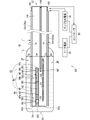
- FIG. 2 is a schematic view of the configuration of the gas sensor 100 including a cross-sectional view taken along the longitudinal direction of the sensor element 10.
- the sensor element 10 is a ceramic structure which is a main component of the gas sensor 100 which detects a predetermined gas component in the gas to be measured and measures the concentration thereof.
- the sensor element 10 is a so-called limit current type gas sensor element.
- the sensor element 10 is a so-called limit current type gas sensor element.
- the gas sensor 100 mainly includes a pump cell power supply 30, a heater power supply 40, and a controller 50.
- the sensor element 10 generally has a structure in which one end side of a long plate-shaped element substrate 1 is covered with a porous tip protective layer 2.
- the element substrate 1 has a long plate-shaped ceramic body 101 as a main structure, and is further provided with a main surface protective layer 170 on two main surfaces of the ceramic body 101.
- the tip protection layer 2 is provided on the end surface (the tip surface 101e of the ceramic body 101) on the one tip side and the outside of the four side surfaces.
- the four side surfaces of the sensor element 10 (or the element base 1, the ceramic body 101) excluding both end faces in the longitudinal direction are simply referred to as side surfaces of the sensor element 10 (or the element base 1, the ceramic body 101). ..
- the ceramic body 101 is made of ceramics containing zirconia (yttrium-stabilized zirconia), which is an oxygen ion conductive solid electrolyte, as a main component. Further, various components of the sensor element 10 are provided inside and outside the ceramic body 101. The ceramic body 101 having such a structure is dense and airtight.
- the configuration of the sensor element 10 shown in FIG. 2 is merely an example, and the specific configuration of the sensor element 10 is not limited to this.
- the sensor element 10 shown in FIG. 2 is a so-called series three-chamber structure type gas sensor element having a first internal vacancy 102, a second internal vacancy 103, and a third internal vacancy 104 inside the ceramic body 101.
- the first internal vacancy 102 is a gas that opens to the outside on the one end E1 side of the ceramic body 101 (strictly speaking, communicates with the outside via the tip protection layer 2). It communicates with the introduction port 105 through the first diffusion rate control unit 110 and the second diffusion rate control unit 120, and the second internal vacancy 103 communicates with the first internal vacancy 102 through the third diffusion rate control unit 130.
- the third internal vacancy 104 communicates with the second internal vacancy 103 through the fourth diffusion rate-determining unit 140.
- the route from the gas introduction port 105 to the third internal vacant room 104 is also referred to as a gas distribution unit.
- the distribution portion is provided in a straight line along the longitudinal direction of the ceramic body 101.
- the first diffusion-controlled unit 110, the second diffusion-controlled unit 120, the third diffusion-controlled unit 130, and the fourth diffusion-controlled unit 140 are all provided as two slits at the top and bottom of the drawing.
- the first diffusion-controlled unit 110, the second diffusion-controlled unit 120, the third diffusion-controlled unit 130, and the fourth diffusion-controlled unit 140 impart a predetermined diffusion resistance to the passing gas to be measured.
- a buffer space 115 having an effect of buffering the pulsation of the gas to be measured is provided between the first diffusion-controlled unit 110 and the second diffusion-controlled unit 120.
- the outer surface of the ceramic body 101 is provided with the external pump electrode 141, and the first internal vacancy 102 is provided with the internal pump electrode 142. Further, the second internal vacancy 103 is provided with an auxiliary pump electrode 143, and the third internal vacancy 104 is provided with a measurement electrode 145 which is a direct detection unit for the gas component to be measured.
- the other end E2 side of the ceramic body 101 is provided with a reference gas introduction port 106 through which the reference gas is introduced to the outside, and a reference electrode 147 is provided in the reference gas introduction port 106. Has been done.
- the NOx gas concentration in the gas to be measured is calculated by the following process.
- the gas to be measured introduced into the first internal vacancy 102 has an oxygen concentration adjusted to be substantially constant by the pumping action (pumping or pumping out oxygen) of the main pump cell P1, and then the second interior. It is introduced in the vacant room 103.
- the main pump cell P1 is an electrochemical pump cell composed of an external pump electrode 141, an internal pump electrode 142, and a ceramic layer 101a which is a portion of a ceramic body 101 existing between the two electrodes.
- oxygen in the gas to be measured is pumped out to the outside of the element by the pumping action of the auxiliary pump cell P2, which is also an electrochemical pump cell, and the gas to be measured is sufficiently low oxygen. It is in a divided state.
- the auxiliary pump cell P2 is composed of an external pump electrode 141, an auxiliary pump electrode 143, and a ceramic layer 101b which is a portion of a ceramic body 101 existing between the two electrodes.
- the external pump electrode 141, the internal pump electrode 142, and the auxiliary pump electrode 143 are formed as a porous cermet electrode (for example, a cermet electrode of Pt containing 1% Au and ZrO2).
- the internal pump electrode 142 and the auxiliary pump electrode 143 that come into contact with the gas to be measured are formed by using a material having a weakened or non-reducing ability to the NOx component in the gas to be measured.
- the measurement electrode 145 is a porous cermet electrode that also functions as a NOx reduction catalyst that reduces NOx existing in the atmosphere in the third internal vacancy 104.
- the potential difference between the measurement electrode 145 and the reference electrode 147 is kept constant. Then, the oxygen ions generated by the above-mentioned reduction or decomposition are pumped out to the outside of the device by the measurement pump cell P3.
- the measurement pump cell P3 is composed of an external pump electrode 141, a measurement electrode 145, and a ceramic layer 101c which is a portion of a ceramic body 101 existing between the two electrodes.
- the measurement pump cell P3 is an electrochemical pump cell that pumps out oxygen generated by decomposition of NOx in the atmosphere around the measurement electrode 145.
- Pumping (pumping or pumping oxygen) in the main pump cell P1, the auxiliary pump cell P2, and the measuring pump cell P3 is pumped between the electrodes provided in each pump cell by the pump cell power supply (variable power supply) 30 under the control of the controller 50. It is realized by applying the voltage required for. In the case of the measurement pump cell P3, a voltage is applied between the external pump electrode 141 and the measurement electrode 145 so that the potential difference between the measurement electrode 145 and the reference electrode 147 is maintained at a predetermined value. ..
- the pump cell power supply 30 is usually provided for each pump cell.
- the controller 50 detects the pump current Ip2 flowing between the measurement electrode 145 and the external pump electrode 141 according to the amount of oxygen pumped out by the measurement pump cell P3, and determines the current value (NOx signal) of the pump current Ip2. ,
- the NOx concentration in the gas to be measured is calculated based on the linear relationship with the concentration of the decomposed NOx.
- the gas sensor 100 includes a plurality of electrochemical sensor cells (not shown) that detect a potential difference between each pump electrode and the reference electrode 147, and the controller 50 controls each pump cell. It is performed based on the detection signal of the sensor cell.
- the heater 150 is embedded inside the ceramic body 101.
- the heater 150 is provided on the lower side of the gas flow section in FIG. 2 as viewed from the drawing, over a range from the vicinity of one end E1 to at least the formation positions of the measurement electrode 145 and the reference electrode 147.
- the heater 150 is provided mainly for the purpose of heating the sensor element 10 in order to increase the oxygen ion conductivity of the solid electrolyte constituting the ceramic body 101 when the sensor element 10 is used. More specifically, the heater 150 is provided so as to be surrounded by an insulating layer 151.
- the heater 150 is a resistance heating element made of, for example, platinum.
- the heater 150 generates heat by supplying power from the heater power supply 40 under the control of the controller 50.
- the sensor element 10 is heated by the heater 150 so that the temperature in the range from at least the first internal vacancy 102 to the second internal vacancy 103 is 500 ° C. or higher.
- the entire gas flow section from the gas introduction port 105 to the third internal vacant room 104 may be heated to 500 ° C. or higher. These are for increasing the oxygen ion conductivity of the solid electrolyte constituting each pump cell so that the capacity of each pump cell can be suitably exhibited.
- the temperature near the first internal vacant room 102 which is the highest temperature, is about 700 ° C. to 800 ° C.
- the side on which the main pump cell P1, the auxiliary pump cell P2, and the measurement pump cell P3 are provided which are located on the upper side in the drawing in FIG.
- the main surface (or the outer surface of the sensor element 10 provided with the main surface) is referred to as a pump surface 1p
- the outer surface of 10) is referred to as a heater surface 1h.
- the pump surface 1p is the main surface of the gas inlet 105, the three internal vacant rooms, and the side closer to each pump cell than the heater 150
- the heater surface 1h is the gas inlet 105, the three internal vacant spaces. The main surface of the chamber and the side closer to the heater 150 than each pump cell.
- a plurality of electrode terminals 160 for making an electrical connection between the sensor element 10 and the outside are formed on the other end E2 side on each main surface of the ceramic body 101. These electrode terminals 160 pass through a lead wire (not shown) provided inside the ceramic body 101, and have a predetermined correspondence relationship with the above-mentioned five electrodes, both ends of the heater 150, and a lead wire for detecting heater resistance (not shown). It is electrically connected. Therefore, the voltage is applied from the pump cell power supply 30 to each pump cell of the sensor element 10 and the heater 150 is heated by the power supply from the heater power supply 40 through the electrode terminal 160.
- the main surface protective layers 170 (170a, 170b) described above are provided on the pump surface 1p and the heater surface 1h of the ceramic body 101.
- the main surface protective layer 170 is a layer made of alumina, having a thickness of about 5 ⁇ m to 30 ⁇ m and having pores having a porosity of about 20% to 40%, and is a layer having pores on the main surface (pump surface 1p) of the ceramic body 101. It is provided for the purpose of preventing foreign matter and toxic substances from adhering to the heater surface 1h) and the external pump electrode 141 provided on the pump surface 1p side. Therefore, the main surface protective layer 170a on the pump surface 1p side also functions as a pump electrode protective layer that protects the external pump electrode 141.
- the porosity is determined by applying a known image processing method (binarization, etc.) to the SEM (scanning electron microscope) image of the evaluation object.
- the main surface protective layer 170 is provided over substantially the entire surface of the pump surface 1p and the heater surface 1h except that a part of the electrode terminal 160 is exposed, but this is merely an example and is shown in FIG. More than the case, the main surface protective layer 170 may be provided unevenly in the vicinity of the external pump electrode 141 on the one end E1 side.
- the tip protection layer 2 is provided on the outermost peripheral portion within a predetermined range from one end portion E1 of the element substrate 1 having the above-described configuration.
- the tip protective layer 2 is provided by surrounding a portion of the element substrate 1 that becomes hot (up to about 700 ° C. to 800 ° C.) when the gas sensor 100 is used, thereby ensuring water resistance in the portion. This is to prevent cracks (water-covered cracks) from occurring in the element substrate 1 due to thermal shock caused by a local temperature drop due to the portion being directly exposed to water.
- the tip protective layer 2 is provided to prevent toxic substances such as Mg from entering the inside of the sensor element 10 and to ensure toxicity resistance.
- the tip protective layer 2 is provided in order from the inside so as to cover the tip surface 101e on the one end E1 side of the element substrate 1 and the four side surfaces (on the outer circumference of the element substrate 1 on the one end E1 side). ..
- the portion on the tip surface 101e side is particularly referred to as the tip portion 2e
- the portion on the pump surface 1p side is particularly referred to as the pump surface portion 2p
- the portion on the heater surface 1h side is particularly referred to as the heater surface portion 2h.
- the tip protective layer 2 is made of alumina so as to have a porosity of 10% to 40%.
- the tip protective layer 2 has a function of suppressing heat conduction from the outside to the element substrate 1 by being provided as a layer having a low porosity and a low thermal conductivity.
- the tip protective layer 2 is arranged with two main surfaces (pump surface 1p and heater surface 1h) of the element substrate 1 which is the main surface to be formed thereof and the heater 150 while ensuring the water resistance of the sensor element 10. It is formed to a thickness based on the relationship. Details on this point will be described later.
- the tip protective layer 2 is formed by sequentially spraying (plasma spraying) its constituent materials onto the element substrate 1. This is to develop an anchor effect between the element substrate 1 and the tip protective layer 2 and to secure the adhesiveness (adhesion) of the tip protective layer 2 to the element substrate 1.
- the tip protection layer 2 has a laminated structure>
- the sensor element 10 in which the tip protection layer 2 is a single layer is shown, but the tip protection layer 2 may have a laminated structure in which two or more layers (unit layers) are laminated. ..
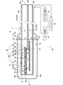
- FIG. 3 is a diagram showing a gas sensor 100 when the tip protection layer 2 has a two-layer structure of an inner tip protection layer 2a and an outer tip protection layer 2b.
- the inner tip protective layer 2a is the same layer as the tip protective layer 2 in the sensor element 10 shown in FIG. 2, and the outer tip protective layer 2b is the inner tip protective layer 2a. It shall be provided in a surrounding manner.
- the outer tip protective layer 2b is provided with alumina so as to have a porosity of 10% to 40%, which is smaller than the other layers provided inside the outer tip protective layer 2b (in the case shown in FIG. 3, the inner tip protective layer 2a). It becomes. As a result, in the tip protective layer 2 shown in FIG. 3, a layer having a thermal conductivity smaller than that of the outer tip protective layer 2b is covered with an outer tip protective layer 2b having a porosity smaller than that of the layer. ing.
- the outer tip protective layer 2b is also formed by sequentially spraying (plasma spraying) its constituent materials, like the inner tip protective layer 2a.
- each unit layer has a positional relationship between the pump surface 1p and the heater surface 1h and the heater 150 while ensuring the water resistance of the sensor element 10. It is formed to the thickness based on it. As a result, the total thickness of the tip protection layer 2 becomes a value based on the arrangement relationship.
- a base layer (not shown) may be formed between the element substrate 1 and the inner tip protective layer 2a.
- the base layer is formed at the same time as the element base 1 unlike the inner tip protective layer 2a which is formed by thermal spraying after the element base 1 is completed.
- the thickness (total thickness) of the tip protection layer 2 provided in the sensor element 10 of the gas sensor 100 according to the present embodiment will be described.
- the tip protective layer 2 is formed to have a thickness based on the arrangement relationship between the pump surface 1p, the heater surface 1h, and the heater 150.
- the tip protective layer 2 is provided on each of the pump surface portion 2p and the heater surface portion 2h. It is provided so as to satisfy the equation (1). In such a case, the water resistance of the sensor element 10 is well ensured. More specifically, a water resistance of more than 6 ⁇ L can be obtained.
- the value on the left side of the relational expression will be referred to as a thickness index value.
- the thickness index value has a positive correlation with water resistance. That is, the sensor element 10 having a larger thickness index value can obtain excellent water resistance. More specifically, the term Ts, i ⁇ ⁇ i / Ls that gives the thickness index value is inversely proportional to the distance Ls from the heater 150 to the main surface of the element substrate 1, and is proportional to the thickness Ts, i of the unit layer. Therefore, in the formula (1), on both the pump surface 1p side and the heater surface 1h side, the unit layer constituting the tip protection layer 2 is formed with a thickness commensurate with the distance Ls from the heater 150 to the main surface of the element substrate 1. By providing it, it means that excellent water resistance can be obtained.
- the heater surface 1h is closer to the heater 150 than the pump surface 1p, so that the heater surface 2h is formed with a thickness smaller than that of the pump surface 2p.
- the water resistance of both can be made equivalent.
- the thickness of the unit layer is determined within the range in which the equation (1) is satisfied in both the pump surface portion 2p and the heater surface portion 2h, the water resistance of the sensor element 10 is ensured. Therefore, it can be said that there is little need to provide the tip protection layer 2 with an excessively large thickness. In such a case, there is a concern that the responsiveness and the temperature rising performance will be deteriorated. Therefore, the formula (1) ensures the water resistance without causing the responsiveness and the temperature rising performance to be deteriorated. It can be said that it is a requirement to do so.
- the thickness of the inner tip protective layer 2a and the outer tip protective layer 2b is excessively increased, the thermal load applied to the heater 150 at the time of temperature rise becomes large, and as a result, the sensor element 10 may be cracked. It is not preferable because it occurs. From this point of view, the thickness of the inner tip protective layer 2a is preferably 800 ⁇ m or less, and the thickness of the outer tip protective layer 2b is preferably 400 ⁇ m or less.
- the two main surfaces of the element base 1 of the tip protective layer 2 surrounding the portion of the element base 1 that becomes hot when the gas sensor 100 is used are used.
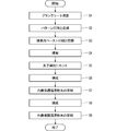
- FIG. 4 is a diagram showing a flow of processing when the sensor element 10 is manufactured, taking as an example a case where the tip protection layer 2 includes an inner tip protection layer 2a and an outer tip protection layer 2b as shown in FIG. ..
- a plurality of blank sheets which are green sheets containing an oxygen ion conductive solid electrolyte such as zirconia as a ceramic component and have no pattern formed, are prepared (not shown). Step S1).
- the blank sheet is provided with a plurality of sheet holes used for positioning during printing and laminating.
- the sheet holes are formed in advance by punching with a punching device or the like at the stage of the blank sheet prior to pattern formation.
- the penetrating portion corresponding to the internal space is also provided in advance by the same punching process or the like.
- the thickness of each blank sheet does not have to be the same, and the thickness may be different depending on the corresponding portion of the finally formed element substrate 1.
- step S2 pattern printing / drying processing is performed on each blank sheet (step S2). Specifically, various electrode patterns, heater 150 and insulating layer 151 patterns, electrode terminal 160 patterns, main surface protection layer 170 patterns, internal wiring patterns (not shown), and the like are included. It is formed. Further, at the timing of such pattern printing, a sublimable material for forming the first diffusion-controlled unit 110, the second diffusion-controlled unit 120, the third diffusion-controlled unit 130, and the fourth diffusion-controlled unit 140 ( The disappearing material) is also applied or placed. When forming the base layer, a pattern for forming the base layer is also printed on the blank sheet which becomes the uppermost layer and the lowermost layer after laminating.
- Printing of each pattern is performed by applying a pattern forming paste prepared according to the characteristics required for each forming target to a blank sheet using a known screen printing technique.
- Known drying means can also be used for the drying treatment after printing.
- step S3 the adhesive paste for laminating and adhering the green sheets is printed and dried.
- a known screen printing technique can be used for printing the adhesive paste, and a known drying means can also be used for the drying treatment after printing.
- the green sheets coated with the adhesive are stacked in a predetermined order and crimped by applying predetermined temperature and pressure conditions to form a single laminate (step S4).
- the green sheets to be laminated are stacked and held on a predetermined laminating jig (not shown) while being positioned by the sheet holes, and the laminating jig is heated and pressurized by a laminating machine such as a known hydraulic press. Do by.
- the pressure, temperature, and time for heating and pressurizing depend on the laminating machine used, but appropriate conditions may be set so that good laminating can be achieved.
- a pattern for forming a base layer may be formed on the laminate obtained in the above aspect.
- step S5 When the laminated body is obtained as described above, subsequently, a plurality of parts of the laminated body are cut, and each is cut into a unit body which is finally an individual element substrate 1 (step S5).
- the obtained unit body is fired at a firing temperature of about 1300 ° C. to 1500 ° C. (step S6).
- the element substrate 1 is manufactured. That is, the element substrate 1 is produced by integrally firing the ceramic body 101 made of a solid electrolyte, each electrode, and the main surface protective layer 170.
- each electrode has sufficient adhesion strength by being integrally fired in such an embodiment.
- the inner tip protective layer 2a and the outer tip protective layer 2b are subsequently formed on the element substrate 1.
- a powder (alumina powder) for forming the inner tip protective layer prepared in advance is sprayed on the element substrate 1 with respect to the target position of the inner tip protective layer 2a according to the target formation thickness (step).
- the element substrate 1 on which the coating film is formed is fired (step S8) in the above manner.
- the alumina powder for forming the inner tip protective layer contains the alumina powder having a predetermined particle size distribution and the pore-forming material in a ratio corresponding to the desired porosity, and the element substrate 1 is fired after thermal spraying.
- the inner tip protective layer 2a having a high porosity of 40% to 80% is suitably formed by thermally decomposing the pore-forming material. It should be noted that known techniques can be applied to thermal spraying and firing.
- the speed of thermal spraying may be reduced when the side to be increased in thickness is formed, or the thermal spraying may be performed at the same location. This can be achieved by repeating.
- a powder (alumina powder) for forming the outer tip protective layer which is also prepared in advance and contains alumina powder having a predetermined particle size distribution, is applied to the outer tip of the element substrate 1.
- alumina powder for forming the outer tip protective layer does not contain a pore-forming material.
- Known techniques can also be applied to such thermal spraying. Further, when the thickness of the outer tip protective layer 2b is different between the pump surface 1p side and the heater surface 1h side, the correspondence is the same as when the inner tip protective layer 2a is formed.
- the sensor element 10 can be obtained by the above procedure.
- the obtained sensor element 10 is housed in a predetermined housing and incorporated into the main body (not shown) of the gas sensor 100.
- the sensor element having three internal vacancies is targeted, but it is not essential that the sensor element has a three-chamber structure. That is, the sensor element may have two or one internal vacancies.
- step S7 after the powder for forming the inner tip protective layer is sprayed in step S7, the powder for forming the outer tip protective layer is sprayed in step S8 after firing in step S8.
- step S8 the order of firing in step S8 and thermal spraying in step S9 may be interchanged.
- the inner tip protective layer 2a and the outer tip protective layer 2b are provided with alumina, and alumina powder is used as a thermal spray material when forming both layers. It is not an essential aspect. Instead of alumina, metal oxides such as zirconia (ZrO 2 ), spinel (MgAl 2 O 4 ), and mullite (Al 6 O1 3 Si 2 ) are used to provide the inner tip protective layer 2a and the outer tip protective layer 2b. It may be an embodiment. In such a case, the powder of those metal oxides may be adopted as a thermal spraying material.
- ZrO 2 zirconia
- MgAl 2 O 4 spinel
- mullite Al 6 O1 3 Si 2
- the porosity ⁇ of the tip protective layer 2 was set to 25%.
- the water resistance was evaluated by 0.1 ⁇ L with respect to the pump surface side of the sensor element 10 while measuring the pump current in the main pump cell P1 in a state where each sensor element 10 was heated to about 500 ° C. to 900 ° C. by the heater 150. Water droplets were dropped one by one, and the maximum amount of water was specified within the range where no abnormality occurred in the measurement output.
- Table 1 lists the distance Ls in each sensor element 10, the thickness Ts and porosity ⁇ of the tip protective layer 2, the thickness index value calculated based on them, and the evaluation result of water resistance. Shown. However, on the pump surface 1p side, since there was no substantial difference between the sensor elements 10 in the evaluation result of water resistance, only one representative result is shown.
- FIG. 5 is a diagram in which the evaluation results of water resistance according to Example 1 shown in Table 1 are plotted against the thickness index value. From FIG. 5, it can be seen that the thickness index value has a positive correlation with the water resistance. It is also confirmed that when the thickness index value exceeds 0.1, the water resistance of more than 6 ⁇ L is obtained.
- the result shown in FIG. 5 applies the evaluation result on the heater surface 1h side to the correlation shown by the evaluation result on the pump surface 1p side without any problem.
- the tip protective layer 2 is provided so that the thickness index value satisfies the equation (1), the water resistance is suitably secured without distinguishing between the pump surface 1p side and the heater surface 1h side. Which indicates that.
- the water resistance value is as high as 10.9 ⁇ L even if the thickness Ts is 300 ⁇ m, whereas on the pump surface side where the distance Ls is large, Even when the thickness Ts is set to 562 ⁇ m, which is nearly twice that thickness, the water resistance value remains at 8.8 ⁇ L. This is considered to suggest that the larger the distance between the heater 150 and both main surfaces of the element substrate 1, the larger the temperature difference inside the sensor element 10, and the worse the thermal shock resistance.
- Example 2 As Example 2, a sensor element 10 in which the tip protective layer 2 was composed of two layers, an inner tip protective layer 2a and an outer tip protective layer 2b, was produced, and the water resistance of the pump surface 1p side and the heater surface 1h side was evaluated.
- the inner tip protective layer 2a was formed so that the thickness Ts1 was 600 ⁇ m and the porosity ⁇ 1 was 50% on both the pump surface 1p side and the heater surface 1h side. Further, the outer tip protective layer 2b is formed so that the thickness Ts2 is 200 ⁇ m and the porosity ⁇ 2 is 20% on both the pump surface 1p side and the heater surface 1h side.
- Table 2 shows the distance Ls between the pump surface 1p side and the heater surface 1h side, the thickness Ts1 and porosity ⁇ 1 of the inner tip protective layer 2a (“the first layer of the protective layer” in Table 2), and the outer tip protective layer 2b.
- the thickness Ts2 and porosity ⁇ 2 of (“second layer of protective layer” in Table 2), the thickness index value calculated based on them, and the evaluation result of water resistance are shown in a list.
- the thickness index value satisfied the formula (1) on both the pump surface 1p side and the heater surface 1h side, and water resistance of 6 ⁇ L or more was obtained.
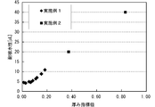
- FIG. 6 is a diagram in which the evaluation results of water resistance according to Example 2 shown in Table 2 are plotted against the thickness index value together with the evaluation results of Example 1.
- the thickness index value has a positive correlation with the water resistance. This means that even when the tip protection layer 2 has a laminated structure of a plurality of unit layers, if each layer is provided so that the thickness index value satisfies the formula (1), the water resistance can be improved. It shows that it is secured well.
Landscapes
- Chemical & Material Sciences (AREA)
- Life Sciences & Earth Sciences (AREA)
- Health & Medical Sciences (AREA)
- Physics & Mathematics (AREA)
- Chemical Kinetics & Catalysis (AREA)
- Electrochemistry (AREA)
- Molecular Biology (AREA)
- Analytical Chemistry (AREA)
- Biochemistry (AREA)
- General Health & Medical Sciences (AREA)
- General Physics & Mathematics (AREA)
- Immunology (AREA)
- Pathology (AREA)
- Measuring Oxygen Concentration In Cells (AREA)
Abstract
センサ素子の素子基体が、検知部が備わる側の端部から所定範囲の外周部に1または複数の単位層からなる多孔質層である先端保護層を備え、素子基体の一方主面または他方主面の上に設けられた先端保護層における、素子基体の側からi番目の単位層(i=1~n:nは自然数)の厚みをTs,i(単位:μm)とし、当該単位層の気孔率をρi(単位:%)とし、ヒータから素子基体の当該一方主面または他方主面までの距離をLs(単位:mm)とし、一方主面を対象とする場合にs=pとし、他方主面を対象とする場合にs=hとするとき、先端保護層のうち一方主面または他方主面の上に設けられる部分について、Ts,i、ρi、Lsが所定の関係式をみたすようにした。
Description
本発明は、ガスセンサのセンサ素子に関し、特にその表面保護層に関する。
従来より、内燃機関からの排ガスなどの被測定ガス中に含まれる所望ガス成分の濃度を知るためのガスセンサとして、ジルコニア(ZrO2)等の酸素イオン伝導性を有する固体電解質からなり、表面や内部にいくつかの電極を備えるセンサ素子を有するものが、広く知られている。係るセンサ素子として、長尺板状の素子形状を有し、かつ、被測定ガスを導入する部分が備わる側の端部に、多孔質体からなる保護層(多孔質保護層)が設けられるものが公知である(例えば、特許文献1参照)。
センサ素子の表面に保護層を設けるのは、ガスセンサの使用時におけるセンサ素子の耐被水性を確保するためである。具体的には、内部に備わるヒータによって加熱された状態にあるセンサ素子の表面に水滴が付着した場合に、水滴からの熱(冷熱)に起因する熱衝撃がセンサ素子に作用して、センサ素子が割れてしまう、被水割れを防止するためである。
特許文献1に開示されているような板状のセンサ素子に保護層を一様に設けた場合、上下の主面側の間において耐熱衝撃性に差があり、ヒータとの距離が遠い主面の方が近い主面よりも熱衝撃に弱い傾向がある。
保護層の厚みを増加させることで耐熱衝撃性を向上させる対応が考えられるが、係る厚みの増加は、センサ素子の応答性や昇温性能の低下につながる。
本発明は、上記課題に鑑みてなされたものであり、所望される耐被水性に応じた厚みにて保護層を備えるガスセンサのセンサ素子を提供することを目的とする。
上記課題を解決するため、本発明の第1の態様は、ガスセンサのセンサ素子であって、測定対象ガス成分の検知部と、前記センサ素子を加熱するためのヒータとを内部に備えたセラミックス構造体である素子基体と、前記素子基体のうち、前記検知部が備わる側の端部から所定範囲の外周部に設けられた、1または複数の単位層からなる多孔質層である先端保護層と、を備え、前記素子基体の一方主面または他方主面の上に設けられた前記先端保護層における、前記素子基体の側からi番目の前記単位層(i=1~n:nは自然数)の厚みをTs,i(単位:μm)とし、当該単位層の気孔率をρi(単位:%)とし、前記ヒータから前記素子基体の当該一方主面または他方主面までの距離をLs(単位:mm)とし、前記一方主面を対象とする場合にs=pとし、前記他方主面を対象とする場合にs=hとするとき、前記先端保護層は前記一方主面または他方主面の上において、

をみたすように設けられてなる、ことを特徴とする。
本発明の第2の態様は、第1の態様に係るセンサ素子であって、n=2であり、ρ1が40%~80%であり、ρ2がρ1よりも小さく10%~40%である、ことを特徴とする。
本発明の第1および第2の態様によれば、応答性や昇温性能の低下を招来することなくセンサ素子の耐被水性を良好に確保することができる。
<センサ素子およびガスセンサの概要>
図1は、本発明の実施の形態に係るセンサ素子(ガスセンサ素子)10の概略的な外観斜視図である。また、図2は、センサ素子10の長手方向に沿った断面図を含むガスセンサ100の構成の概略図である。センサ素子10は、被測定ガス中の所定ガス成分を検知しその濃度を測定するガスセンサ100の、主たる構成要素であるセラミックス構造体である。センサ素子10は、いわゆる限界電流型のガスセンサ素子である。センサ素子10は、いわゆる限界電流型のガスセンサ素子である。
図1は、本発明の実施の形態に係るセンサ素子(ガスセンサ素子)10の概略的な外観斜視図である。また、図2は、センサ素子10の長手方向に沿った断面図を含むガスセンサ100の構成の概略図である。センサ素子10は、被測定ガス中の所定ガス成分を検知しその濃度を測定するガスセンサ100の、主たる構成要素であるセラミックス構造体である。センサ素子10は、いわゆる限界電流型のガスセンサ素子である。センサ素子10は、いわゆる限界電流型のガスセンサ素子である。
ガスセンサ100は、センサ素子10のほか、ポンプセル電源30と、ヒータ電源40と、コントローラ50とを主として備える。
図1に示すように、センサ素子10は概略、長尺板状の素子基体1の一方端部側が、多孔質の先端保護層2にて被覆された構成を有する。
素子基体1は概略、図2に示すように、長尺板状のセラミックス体101を主たる構造体とするとともに、該セラミックス体101の2つの主面上には主面保護層170を備え、さらに、センサ素子10においては、一先端部側の端面(セラミックス体101の先端面101e)および4つの側面の外側に先端保護層2が設けられてなる。なお、以降においては、センサ素子10(もしくは素子基体1、セラミックス体101)の長手方向における両端面を除く4つの側面を単に、センサ素子10(もしくは素子基体1、セラミックス体101)の側面と称する。
セラミックス体101は、酸素イオン伝導性固体電解質であるジルコニア(イットリウム安定化ジルコニア)を主成分とするセラミックスからなる。また、係るセラミックス体101の外部および内部には、センサ素子10の種々の構成要素が設けられてなる。係る構成を有するセラミックス体101は、緻密かつ気密なものである。なお、図2に示すセンサ素子10の構成はあくまで例示であって、センサ素子10の具体的構成はこれに限られるものではない。
図2に示すセンサ素子10は、セラミックス体101の内部に第一の内部空室102と第二の内部空室103と第三の内部空室104とを有する、いわゆる直列三室構造型のガスセンサ素子である。すなわち、センサ素子10においては概略、第一の内部空室102が、セラミックス体101の一方端部E1側において外部に対し開口する(厳密には先端保護層2を介して外部と連通する)ガス導入口105と第一の拡散律速部110、第二の拡散律速部120を通じて連通しており、第二の内部空室103が第三の拡散律速部130を通じて第一の内部空室102と連通しており、第三の内部空室104が第四の拡散律速部140を通じて第二の内部空室103と連通している。なお、ガス導入口105から第三の内部空室104に至るまでの経路を、ガス流通部とも称する。本実施の形態に係るセンサ素子10においては、係る流通部がセラミックス体101の長手方向に沿って一直線状に設けられてなる。
第一の拡散律速部110、第二の拡散律速部120、第三の拡散律速部130、および第四の拡散律速部140はいずれも、図面視上下2つのスリットとして設けられている。第一の拡散律速部110、第二の拡散律速部120、第三の拡散律速部130、および第四の拡散律速部140は、通過する被測定ガスに対して所定の拡散抵抗を付与する。なお、第一の拡散律速部110と第二の拡散律速部120の間には、被測定ガスの脈動を緩衝する効果を有する緩衝空間115が設けられている。
また、セラミックス体101の外面には外部ポンプ電極141が備わり、第一の内部空室102には内部ポンプ電極142が備わっている。さらには、第二の内部空室103には補助ポンプ電極143が備わり、第三の内部空室104には、測定対象ガス成分の直接の検知部である測定電極145が備わっている。加えて、セラミックス体101の他方端部E2側には、外部に連通し基準ガスが導入される基準ガス導入口106が備わっており、該基準ガス導入口106内には、基準電極147が設けられている。
例えば、係るセンサ素子10の測定対象が被測定ガス中のNOxである場合であれば、以下のようなプロセスによって、被測定ガス中のNOxガス濃度が算出される。
まず、第一の内部空室102に導入された被測定ガスは、主ポンプセルP1のポンピング作用(酸素の汲み入れ或いは汲み出し)によって、酸素濃度が略一定に調整されたうえで、第二の内部空室103に導入される。主ポンプセルP1は、外部ポンプ電極141と、内部ポンプ電極142と、両電極の間に存在するセラミックス体101の部分であるセラミックス層101aとによって構成される電気化学的ポンプセルである。第二の内部空室103においては、同じく電気化学的ポンプセルである、補助ポンプセルP2のポンピング作用により、被測定ガス中の酸素が素子外部へと汲み出されて、被測定ガスが十分な低酸素分圧状態とされる。補助ポンプセルP2は、外部ポンプ電極141と、補助ポンプ電極143と、両電極の間に存在するセラミックス体101の部分であるセラミックス層101bとによって構成される。
外部ポンプ電極141、内部ポンプ電極142、および補助ポンプ電極143は、多孔質サーメット電極(例えば、Auを1%含むPtとZrO2とのサーメット電極)として形成されてなる。なお、被測定ガスに接触する内部ポンプ電極142および補助ポンプ電極143は、被測定ガス中のNOx成分に対する還元能力を弱めた、あるいは、還元能力のない材料を用いて形成される。
補助ポンプセルP2によって低酸素分圧状態とされた被測定ガス中のNOxは、第三の内部空室104に導入され、第三の内部空室104に設けられた測定電極145において還元ないし分解される。測定電極145は、第三の内部空室104内の雰囲気中に存在するNOxを還元するNOx還元触媒としても機能する多孔質サーメット電極である。係る還元ないし分解の際には、測定電極145と基準電極147との間の電位差が、一定に保たれている。そして、上述の還元ないし分解によって生じた酸素イオンが、測定用ポンプセルP3によって素子外部へと汲み出される。測定用ポンプセルP3は、外部ポンプ電極141と、測定電極145と、両電極の間に存在するセラミックス体101の部分であるセラミックス層101cとによって構成される。測定用ポンプセルP3は、測定電極145の周囲の雰囲気中におけるNOxの分解によって生じた酸素を汲み出す電気化学的ポンプセルである。
主ポンプセルP1、補助ポンプセルP2、および測定用ポンプセルP3におけるポンピング(酸素の汲み入れ或いは汲み出し)は、コントローラ50による制御のもと、ポンプセル電源(可変電源)30によって各ポンプセルに備わる電極の間にポンピングに必要な電圧が印加されることにより、実現される。測定用ポンプセルP3の場合であれば、測定電極145と基準電極147との間の電位差が所定の値に保たれるように、外部ポンプ電極141と測定電極145との間に電圧が印加される。ポンプセル電源30は通常、各ポンプセル毎に設けられる。
コントローラ50は、測定用ポンプセルP3により汲み出される酸素の量に応じて測定電極145と外部ポンプ電極141との間を流れるポンプ電流Ip2を検出し、このポンプ電流Ip2の電流値(NOx信号)と、分解されたNOxの濃度との間に線型関係があることに基づいて、被測定ガス中のNOx濃度を算出する。
なお、好ましくは、ガスセンサ100は、それぞれのポンプ電極と基準電極147との間の電位差を検知する、図示しない複数の電気化学的センサセルを備えており、コントローラ50による各ポンプセルの制御は、それらのセンサセルの検出信号に基づいて行われる。
また、センサ素子10においては、セラミックス体101の内部にヒータ150が埋設されている。ヒータ150は、ガス流通部の図2における図面視下方側において、一方端部E1近傍から少なくとも測定電極145および基準電極147の形成位置までの範囲にわたって設けられる。ヒータ150は、センサ素子10の使用時に、セラミックス体101を構成する固体電解質の酸素イオン伝導性を高めるべく、センサ素子10を加熱することを主たる目的として、設けられてなる。より詳細には、ヒータ150はその周囲を絶縁層151に囲繞される態様にて設けられてなる。
ヒータ150は、例えば白金などからなる抵抗発熱体である。ヒータ150は、コントローラ50による制御のもと、ヒータ電源40からの給電により発熱する。
本実施の形態に係るセンサ素子10はその使用時、ヒータ150によって、少なくとも第一の内部空室102から第二の内部空室103に至る範囲の温度が500℃以上となるように、加熱される。さらには、ガス導入口105から第三の内部空室104に至るまでのガス流通部全体が500℃以上となるように、加熱される場合もある。これらは、各ポンプセルを構成する固体電解質の酸素イオン伝導性を高め、各ポンプセルの能力が好適に発揮されるようにするためである。係る場合、最も高温となる第一の内部空室102付近の温度は、700℃~800℃程度となる。
以降においては、素子基体1の(セラミックス体101の)2つの主面のうち、図2において図面視上方側に位置する、主に主ポンプセルP1、補助ポンプセルP2、および測定用ポンプセルP3が備わる側の主面(あるいは当該主面が備わるセンサ素子10の外面)をポンプ面1pと称し、図2において図面視下方に位置する、ヒータ150が備わる側の主面(あるいは当該主面が備わるセンサ素子10の外面)をヒータ面1hと称する。換言すれば、ポンプ面1pは、ヒータ150よりもガス導入口105、3つの内部空室、および各ポンプセルに近接する側の主面であり、ヒータ面1hはガス導入口105、3つの内部空室、および各ポンプセルよりもヒータ150に近接する側の主面である。
セラミックス体101のそれぞれの主面上の他方端部E2側には、センサ素子10と外部との間の電気的接続を図るための複数の電極端子160が形成されてなる。これらの電極端子160は、セラミックス体101の内部に備わる図示しないリード線を通じて、上述した5つの電極と、ヒータ150の両端と、図示しないヒータ抵抗検出用のリード線と、所定の対応関係にて電気的に接続されている。よって、センサ素子10の各ポンプセルに対するポンプセル電源30から電圧の印加や、ヒータ電源40からの給電によるヒータ150の加熱は、電極端子160を通じてなされる。
さらに、センサ素子10においては、セラミックス体101のポンプ面1pおよびヒータ面1hに、上述した主面保護層170(170a、170b)が備わっている。主面保護層170は、アルミナからなる、厚みが5μm~30μm程度であり、かつ20%~40%程度の気孔率にて気孔が存在する層であり、セラミックス体101の主面(ポンプ面1pおよびヒータ面1h)や、ポンプ面1p側に備わる外部ポンプ電極141に対する、異物や被毒物質の付着を防ぐ目的で設けられてなる。それゆえ、ポンプ面1p側の主面保護層170aは、外部ポンプ電極141を保護するポンプ電極保護層としても機能するものである。
なお、本実施の形態において、気孔率は、評価対象物のSEM(走査電子顕微鏡)像に対し公知の画像処理手法(二値化処理など)を適用することで求めるものとする。
図2においては、電極端子160の一部を露出させるほかはポンプ面1pおよびヒータ面1hの略全面にわたって主面保護層170が設けられてなるが、これはあくまで例示であり、図2に示す場合よりも、主面保護層170は、一方端部E1側の外部ポンプ電極141近傍に偏在させて設けられてもよい。
<先端保護層の詳細>
センサ素子10においては、上述のような構成を有する素子基体1の一方端部E1から所定範囲の最外周部に、先端保護層2が設けられてなる。
センサ素子10においては、上述のような構成を有する素子基体1の一方端部E1から所定範囲の最外周部に、先端保護層2が設けられてなる。
先端保護層2を設けるのは、素子基体1のうちガスセンサ100の使用時に高温(最高で700℃~800℃程度)となる部分を囲繞することによって、当該部分における耐被水性を確保し、当該部分が直接に被水することによる局所的な温度低下に起因した熱衝撃により素子基体1にクラック(被水割れ)が生じることを、抑制するためである。
加えて、先端保護層2は、センサ素子10の内部にMgなどの被毒物質が入り込むことを防ぐ、耐被毒性の確保のためにも、設けられてなる。
先端保護層2は、素子基体1の一方端部E1側の先端面101eと4つの側面とを覆うように(素子基体1の一方端部E1側の外周に)、内側から順に設けられてなる。先端保護層2のうち、先端面101e側の部分を特に先端部2eと称し、ポンプ面1p側の部分を特にポンプ面部2pと称し、ヒータ面1h側の部分を特にヒータ面部2hと称する。
先端保護層2は、アルミナにて、10%~40%の気孔率を有するように、設けられてなる。先端保護層2は、気孔率が大きい低熱伝導率の層として設けられることで、外部から素子基体1への熱伝導を抑制する機能を有してなる。
また、先端保護層2は、センサ素子10における耐被水性を確保しつつ、その主たる形成対象面である素子基体1の2つの主面(ポンプ面1pおよびヒータ面1h)とヒータ150との配置関係を踏まえた厚みに形成される。この点についての詳細は後述する。
先端保護層2は、素子基体1に対し、その構成材料を順次に溶射(プラズマ溶射)することで形成される。これは、素子基体1と先端保護層2の間にアンカー効果を発現させ、素子基体1に対する先端保護層2の接着性(密着性)を、確保するためである。
<先端保護層が積層構造を有する場合>
図2においては、先端保護層2が単一層であるセンサ素子10を示していたが、先端保護層2は、2以上の層(単位層)が積層された積層構造を有していてもよい。
図2においては、先端保護層2が単一層であるセンサ素子10を示していたが、先端保護層2は、2以上の層(単位層)が積層された積層構造を有していてもよい。
図3は、先端保護層2が内側先端保護層2aと外側先端保護層2bの2層構成を有する場合のガスセンサ100を示す図である。ただし、図3に示す場合においては、内側先端保護層2aは図2に示したセンサ素子10における先端保護層2と同一の層であり、外側先端保護層2bは、係る内側先端保護層2aを囲繞する態様にて設けられてなるものとする。
外側先端保護層2bは、アルミナにて、その内側に備わる他の層(図3に示す場合においては内側先端保護層2a)よりも小さい10%~40%の気孔率を有するように、設けられてなる。これにより、図3に示す先端保護層2においては、外側先端保護層2bよりも熱伝導率の小さい層が、当該層よりも気孔率の小さい外側先端保護層2bに、被覆された構成となっている。
外側先端保護層2bも、内側先端保護層2aと同様、その構成材料を順次に溶射(プラズマ溶射)することで形成される。
また、このように先端保護層2が積層構造を有する場合も、それぞれの単位層は、センサ素子10における耐被水性を確保しつつ、ポンプ面1pおよびヒータ面1hとヒータ150との配置関係を踏まえた厚みに形成される。結果として、先端保護層2の総厚は、当該配置関係を踏まえた値となる。
なお、内側先端保護層2aの密着性をより高める目的で、素子基体1と内側先端保護層2aとの間に、図示しない下地層が形成される態様であってもよい。下地層は、素子基体1の完成後に溶射にて形成される内側先端保護層2aなどとは異なり、素子基体1と同時に形成される。
<先端保護層の厚み>
次に、本実施の形態に係るガスセンサ100のセンサ素子10に備わる先端保護層2の厚み(総厚)について説明する。本実施の形態においては、上述のように、先端保護層2は、ポンプ面1pおよびヒータ面1hとヒータ150との配置関係を踏まえた厚みに形成される。
次に、本実施の形態に係るガスセンサ100のセンサ素子10に備わる先端保護層2の厚み(総厚)について説明する。本実施の形態においては、上述のように、先端保護層2は、ポンプ面1pおよびヒータ面1hとヒータ150との配置関係を踏まえた厚みに形成される。
より詳細には、先端保護層2がn個(nは自然数)の単位層からなるとし、このうち、素子基体1の側からi番目の単位層(i=1~n)の厚みをTs,i(ただし、ポンプ面部2pの厚みを示す場合はs=p、ヒータ面部2hの厚みを示す場合はs=h、単位:μm)とし、当該単位層の気孔率をρi(単位:%)とし、ヒータ150から素子基体1の主面までの距離をLs(ただし、ポンプ面1p側の距離を示す場合はs=p、ヒータ面1h側の厚みを示す場合はs=h、単位:mm)とするとき、先端保護層2は、ポンプ面部2p、ヒータ面部2hのそれぞれにおいて、

なる式(1)をみたすように設けられる。係る場合、センサ素子10における耐被水性が良好に確保される。より詳細には、6μLを上回る耐被水性が得られる。以降、当該関係式の左辺の値を厚み指標値と称する。
なお、図2に示すセンサ素子10のように単位層が1層(i=1)の場合、式(1)の添字iは省略されてもよい。図2においては、Tp,i=Tp、Th,i=Thとしている。また、図3においては、Tp,1=Tp1、Th,1=Th1、Tp,2=Tp2、Th,2=Th2としている。
厚み指標値は耐被水性と正の相関を有することがわかっている。すなわち、厚み指標値が大きいセンサ素子10ほど、優れた耐被水性が得られる。より詳細には、厚み指標値を与えるTs,i・ρi/Lsなる項は、ヒータ150から素子基体1の主面までの距離Lsに反比例し、単位層の厚みTs,iに比例する。それゆえ式(1)は、ポンプ面1p側とヒータ面1h側の双方において、ヒータ150から素子基体1の主面までの距離Lsに見合った厚みにて先端保護層2を構成する単位層を設けることで、優れた耐被水性が得られることを意味している。これは、ヒータ150と素子基体1の両主面との距離が大きいほど、センサ素子10内部における温度差が大きくなり、耐熱衝撃性が劣化することによるものと考えられる。図2や図3に示すセンサ素子10の場合であれば、ヒータ面1hの方がポンプ面1pよりもヒータ150に近いので、ヒータ面部2hをポンプ面部2pよりも小さな厚みにて形成しつつ、両者の耐被水性を同等のものとすることができる。
また、別の見方をすれば、ポンプ面部2p、ヒータ面部2hの双方において式(1)を充足する範囲で単位層の厚みを定めるようにすれば、センサ素子10における耐被水性は確保されることから、過度に大きな厚みにて先端保護層2を設ける必要性は小さいともいえる。そのような場合はむしろ、応答性や昇温性能の低下が懸念されることになるため、式(1)は、応答性や昇温性能の低下を招来することなく、耐被水性についても確保するための要件であるともいえる。
なお、内側先端保護層2aと外側先端保護層2bの厚みを過度に大きくしすぎると、昇温時にヒータ150に加わる熱的負荷が大きくなり、その結果として、センサ素子10が割れてしまうおそれが生じるため、好ましくない。係る観点からは、内側先端保護層2aの厚みは800μm以下とし、外側先端保護層2bの厚みは400μm以下とするのが好ましい。
以上、説明したように、本実施の形態に係るセンサ素子10においては、素子基体1のうちガスセンサ100の使用時に高温となる部分を囲繞する先端保護層2の、素子基体1の2つの主面上における厚みを、式(1)をみたすように定めることで、応答性や昇温性能の低下を招来することなくセンサ素子10の耐被水性を良好に確保することができる。
<センサ素子の製造プロセス>
次に、上述のような構成および特徴を有するセンサ素子10を製造するプロセスの一例について説明する。図4は、先端保護層2が図3に示すように内側先端保護層2aと外側先端保護層2bとを備える場合を例として、センサ素子10を作製する際の処理の流れを示す図である。
次に、上述のような構成および特徴を有するセンサ素子10を製造するプロセスの一例について説明する。図4は、先端保護層2が図3に示すように内側先端保護層2aと外側先端保護層2bとを備える場合を例として、センサ素子10を作製する際の処理の流れを示す図である。
素子基体1の作製に際しては、まず、ジルコニアなどの酸素イオン伝導性固体電解質をセラミックス成分として含み、かつ、パターンが形成されていないグリーンシートであるブランクシート(図示省略)を、複数枚用意する(ステップS1)。
ブランクシートには、印刷時や積層時の位置決めに用いる複数のシート穴が設けられている。係るシート穴は、パターン形成に先立つブランクシートの段階で、パンチング装置による打ち抜き処理などで、あらかじめ形成されている。なお、セラミックス体101の対応する部分に内部空間が形成されることになるグリーンシートの場合、該内部空間に対応する貫通部も、同様の打ち抜き処理などによってあらかじめ設けられる。また、それぞれのブランクシートの厚みは、全て同じである必要はなく、最終的に形成される素子基体1におけるそれぞれの対応部分に応じて、厚みが違えられていてもよい。
各層に対応したブランクシートが用意できると、それぞれのブランクシートに対してパターン印刷・乾燥処理を行う(ステップS2)。具体的には、各種電極のパターンや、ヒータ150および絶縁層151のパターンや、電極端子160のパターンや、主面保護層170のパターンや、図示を省略している内部配線のパターンなどが、形成される。また、係るパターン印刷のタイミングで、第一の拡散律速部110、第二の拡散律速部120、第三の拡散律速部130、および第四の拡散律速部140を形成するための昇華性材料(消失材)の塗布あるいは配置も併せてなされる。なお、下地層を形成する場合は、積層後に最上層および最下層となるブランクシートに対し、下地層を形成するためのパターンの印刷もなされる。
各々のパターンの印刷は、それぞれの形成対象に要求される特性に応じて用意したパターン形成用ペーストを、公知のスクリーン印刷技術を利用してブランクシートに塗布することにより行う。印刷後の乾燥処理についても、公知の乾燥手段を利用可能である。
各ブランクシートに対するパターン印刷が終わると、グリーンシート同士を積層・接着するための接着用ペーストの印刷・乾燥処理を行う(ステップS3)。接着用ペーストの印刷には、公知のスクリーン印刷技術を利用可能であり、印刷後の乾燥処理についても、公知の乾燥手段を利用可能である。
続いて、接着剤が塗布されたグリーンシートを所定の順序に積み重ねて、所定の温度・圧力条件を与えることで圧着させ、一の積層体とする圧着処理を行う(ステップS4)。具体的には、図示しない所定の積層治具に積層対象となるグリーンシートをシート穴により位置決めしつつ積み重ねて保持し、公知の油圧プレス機などの積層機によって積層治具ごと加熱・加圧することによって行う。加熱・加圧を行う圧力・温度・時間については、用いる積層機にも依存するものであるが、良好な積層が実現できるよう、適宜の条件が定められればよい。なお、係る態様にて得られた積層体に対し下地層を形成するためのパターンの形成がなされる態様であってもよい。
上述のようにして積層体が得られると、続いて、係る積層体の複数個所を切断して、それぞれが最終的に個々の素子基体1となる単位体に切り出す(ステップS5)。
続いて、得られた単位体を、1300℃~1500℃程度の焼成温度で焼成する(ステップS6)。これにより素子基体1が作製される。すなわち、素子基体1は、固体電解質からなるセラミックス体101と、各電極と、主面保護層170とが一体焼成されることによって、生成されるものである。なお、係る態様にて一体焼成がなされることで、素子基体1においては、各電極が十分な密着強度を有するものとなっている。
以上の態様にて素子基体1が作製されると、続いて、係る素子基体1に対し、内側先端保護層2aと外側先端保護層2bの形成が行われる。内側先端保護層2aの形成は、あらかじめ用意した内側先端保護層形成用の粉末(アルミナ粉末)を素子基体1における内側先端保護層2aの形成対象位置に対し狙いの形成厚みに応じて溶射(ステップS7)した後、係る態様にて塗布膜が形成された素子基体1を焼成する(ステップS8)ことによって行われる。内側先端保護層形成用のアルミナ粉末には、所定の粒度分布を有するアルミナ粉末と造孔材とが所望する気孔率に応じた割合にて含まれており、溶射後に素子基体1を焼成することによって係る造孔材を熱分解させることで、40%~80%という高い気孔率の内側先端保護層2aが好適に形成されるようになっている。なお、溶射および焼成には公知の技術を適用可能である。
なお、ポンプ面1p側とヒータ面1h側とで、内側先端保護層2aの厚みを違えることは、厚みを大きくしたい側を形成する際に、溶射の速度を落とすことや、同一個所への溶射を繰り返すことなどによって、実現が可能である。
内側先端保護層2aが形成されると、続いて、同じくあらかじめ用意した、所定の粒度分布を有するアルミナ粉末が含まれる外側先端保護層形成用の粉末(アルミナ粉末)を、素子基体1における外側先端保護層2bの形成対象位置に対し狙いの形成厚みに応じて溶射する(ステップS9)ことにより、所望の気孔率の外側先端保護層2bを形成する。外側先端保護層形成用のアルミナ粉末には造孔材は含まれない。係る溶射についても、公知の技術を適用可能である。また、ポンプ面1p側とヒータ面1h側とで、外側先端保護層2bの厚みを違える場合の対応は、内側先端保護層2aの形成時と同様である。
なお、図2に示したように、先端保護層2が単一層として設けられる場合には、上述のステップS9は不要である。
以上の手順によりセンサ素子10が得られる。得られたセンサ素子10は、所定のハウジングに収容され、ガスセンサ100の本体(図示せず)に組み込まれる。
<変形例>
上述の実施の形態においては、3つの内部空室を備えたセンサ素子を対象としているが、センサ素子が3室構造であることは必須ではない。すなわち、センサ素子が、内部空室を2つあるいは1つ備える態様であってもよい。
上述の実施の形態においては、3つの内部空室を備えたセンサ素子を対象としているが、センサ素子が3室構造であることは必須ではない。すなわち、センサ素子が、内部空室を2つあるいは1つ備える態様であってもよい。
また、上述の実施の形態においては、ステップS7における内側先端保護層形成用の粉末の溶射後、ステップS8における焼成を行ったうえで、ステップS9における外側先端保護層形成用の粉末の溶射を行っているが、ステップS8の焼成と、ステップS9の溶射の順序は、入れ替わってもよい。
また、上述の実施の形態においては、内側先端保護層2aおよび外側先端保護層2bをアルミナにて設けることとし、両層を形成する際の溶射材として、アルミナ粉末を用いているが、これは必須の態様ではない。アルミナに代えて、ジルコニア(ZrO2)、スピネル(MgAl2O4)、ムライト(Al6O13Si2)などの金属酸化物を用いて、内側先端保護層2aおよび外側先端保護層2bを設ける態様であってもよい。係る場合は、それらの金属酸化物の粉末を溶射材として採用すればよい。
(実施例1)
実施例1として、先端保護層2を単一層として備え、かつポンプ面部2pにおける先端保護層2の厚みTs(=Tp)が異なる8通りのセンサ素子10を作製し、それぞれの耐被水性を評価した。
実施例1として、先端保護層2を単一層として備え、かつポンプ面部2pにおける先端保護層2の厚みTs(=Tp)が異なる8通りのセンサ素子10を作製し、それぞれの耐被水性を評価した。
より詳細には、素子基体1は、ポンプ面1p側において距離Ls(=Lp)が0.91mmとなり、ヒータ面1h側において距離Ls(=Lh)が0.41mmとなるように作製した。
また、先端保護層2の厚みTsは、ポンプ面部2pについてはTs=Tp=50μm、100μm、200μm、250μm、311.5μm、400μm、431μm、562.5μmの5通りに違えた。一方、ヒータ面部2hはTs=Th=300μmとした。また、先端保護層2の気孔率ρは25%とした。
耐被水性の評価は、ヒータ150によってそれぞれのセンサ素子10をおよそ500℃~900℃に加熱した状態で、主ポンプセルP1におけるポンプ電流を測定しつつセンサ素子10のポンプ面側に対し0.1μLずつ水滴を滴下し、測定出力に異常が生じない範囲における最大水量を特定することにより行った。
表1に、それぞれのセンサ素子10における距離Lsと、先端保護層2の厚みTsおよび気孔率ρと、それらに基づいて算出される厚み指標値と、耐被水性の評価結果とを、一覧にして示す。ただし、ポンプ面1p側については、耐被水性の評価結果についてセンサ素子10同士の間で実質的な差異がなかったので、代表的な1つの結果のみを示している。
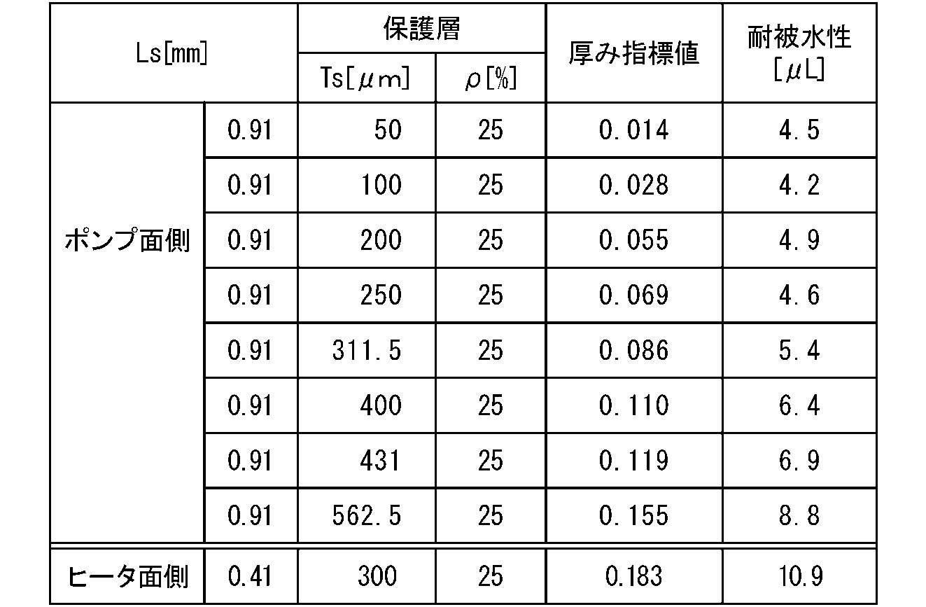
表1に示すように、厚み指標値が式(1)を充足するセンサ素子10においては、6μL以上の耐被水性が得られた。
図5は、表1に示した実施例1に係る耐被水性の評価結果を、厚み指標値に対してプロットした図である。図5からは、厚み指標値は耐被水性と正の相関を有することが把握される。そして、厚み指標値が0.1を超える場合に、6μLを上回る耐被水性が得られていることも確認される。
より詳細には、図5に示す結果は、ポンプ面1p側についての評価結果が示す相関関係に、ヒータ面1h側についての評価結果が問題なく当てはまっているともいえる。このことは厚み指標値が式(1)をみたすように先端保護層2を設けるようにすれば、ポンプ面1p側とヒータ面1h側とを区別することなく、耐被水性が好適に確保されることを示している。
しかも、表1によれば、距離Lsが小さいヒータ面1h側では、厚みTsが300μmであっても耐被水性の値は10.9μLと高いのに対し、距離Lsが大きいポンプ面側においては、厚みTsをその2倍近くの562μmとした場合であっても、耐被水性の値は8.8μLに留まっている。このことは、ヒータ150と素子基体1の両主面との距離が大きいほど、センサ素子10内部における温度差が大きくなり、耐熱衝撃性が劣化することを示唆しているものと考えられる。
(実施例2)
実施例2として、先端保護層2が内側先端保護層2aと外側先端保護層2bの2層からなるセンサ素子10を作製し、ポンプ面1p側とヒータ面1h側の耐被水性を評価した。
実施例2として、先端保護層2が内側先端保護層2aと外側先端保護層2bの2層からなるセンサ素子10を作製し、ポンプ面1p側とヒータ面1h側の耐被水性を評価した。
より詳細には、素子基体1は実施例1と同様、ポンプ面1p側において距離Ls(=Lp)が0.91mmとなり、ヒータ面1h側において距離Ls(=Lh)が0.41mmとなるように作製した。
また、内側先端保護層2aは、ポンプ面1p側、ヒータ面1h側ともに、厚みTs1が600μmであり気孔率ρ1が50%であるように形成した。また、外側先端保護層2bは、ポンプ面1p側、ヒータ面1h側ともに、厚みTs2が200μmであり気孔率ρ2が20%であるように形成した。
表2に、ポンプ面1p側とヒータ面1h側の距離Lsと、内側先端保護層2a(表2においては「保護層1層目」)の厚みTs1および気孔率ρ1と、外側先端保護層2b(表2においては「保護層2層目」)の厚みTs2および気孔率ρ2と、それらに基づいて算出される厚み指標値と、耐被水性の評価結果とを、一覧にして示す。
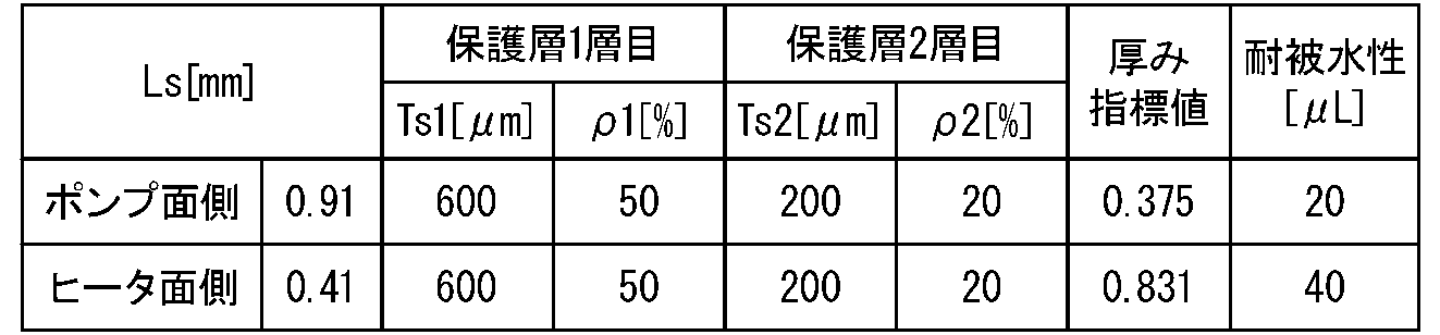
表2に示すように、ポンプ面1p側とヒータ面1h側の双方において、厚み指標値が式(1)を充足するとともに、6μL以上の耐被水性が得られた。
図6は、表2に示した実施例2に係る耐被水性の評価結果を、実施例1の評価結果とともに、厚み指標値に対してプロットした図である。図6においても、図5と同様、厚み指標値は耐被水性と正の相関を有することが把握される。このことはすなわち、先端保護層2を複数の単位層の積層構造とする場合であっても、厚み指標値が式(1)を充足するように各層を設けるようにすれば、耐被水性が良好に確保されることを示している。
Claims (2)
- ガスセンサのセンサ素子であって、
測定対象ガス成分の検知部と、前記センサ素子を加熱するためのヒータとを内部に備えたセラミックス構造体である素子基体と、
前記素子基体のうち、前記検知部が備わる側の端部から所定範囲の外周部に設けられた、1または複数の単位層からなる多孔質層である先端保護層と、
を備え、
前記素子基体の一方主面または他方主面の上に設けられた前記先端保護層における、前記素子基体の側からi番目の前記単位層(i=1~n:nは自然数)の厚みをTs,i(単位:μm)とし、当該単位層の気孔率をρi(単位:%)とし、前記ヒータから前記素子基体の当該一方主面または他方主面までの距離をLs(単位:mm)とし、前記一方主面を対象とする場合にs=pとし、前記他方主面を対象とする場合にs=hとするとき、前記先端保護層は前記一方主面または他方主面の上において、

ことを特徴とするガスセンサのセンサ素子。 - 請求項1に記載のセンサ素子であって、
n=2であり、
ρ1が40%~80%であり、
ρ2がρ1よりも小さく10%~40%である、
ことを特徴とするガスセンサのセンサ素子。
Priority Applications (1)
| Application Number | Priority Date | Filing Date | Title |
|---|---|---|---|
| JP2021508930A JPWO2020195692A1 (ja) | 2019-03-27 | 2020-03-06 | ガスセンサのセンサ素子 |
Applications Claiming Priority (2)
| Application Number | Priority Date | Filing Date | Title |
|---|---|---|---|
| JP2019-061275 | 2019-03-27 | ||
| JP2019061275 | 2019-03-27 |
Publications (1)
| Publication Number | Publication Date |
|---|---|
| WO2020195692A1 true WO2020195692A1 (ja) | 2020-10-01 |
Family
ID=72610064
Family Applications (1)
| Application Number | Title | Priority Date | Filing Date |
|---|---|---|---|
| PCT/JP2020/009572 Ceased WO2020195692A1 (ja) | 2019-03-27 | 2020-03-06 | ガスセンサのセンサ素子 |
Country Status (2)
| Country | Link |
|---|---|
| JP (1) | JPWO2020195692A1 (ja) |
| WO (1) | WO2020195692A1 (ja) |
Citations (2)
| Publication number | Priority date | Publication date | Assignee | Title |
|---|---|---|---|---|
| JP2016065850A (ja) * | 2014-03-28 | 2016-04-28 | 日本碍子株式会社 | 膜接合構造体、その製法及びガスセンサ |
| JP2017187482A (ja) * | 2016-03-30 | 2017-10-12 | 日本碍子株式会社 | センサ素子及びガスセンサ |
-
2020
- 2020-03-06 JP JP2021508930A patent/JPWO2020195692A1/ja active Pending
- 2020-03-06 WO PCT/JP2020/009572 patent/WO2020195692A1/ja not_active Ceased
Patent Citations (2)
| Publication number | Priority date | Publication date | Assignee | Title |
|---|---|---|---|---|
| JP2016065850A (ja) * | 2014-03-28 | 2016-04-28 | 日本碍子株式会社 | 膜接合構造体、その製法及びガスセンサ |
| JP2017187482A (ja) * | 2016-03-30 | 2017-10-12 | 日本碍子株式会社 | センサ素子及びガスセンサ |
Also Published As
| Publication number | Publication date |
|---|---|
| JPWO2020195692A1 (ja) | 2021-12-09 |
Similar Documents
| Publication | Publication Date | Title |
|---|---|---|
| JP7089990B2 (ja) | センサ素子 | |
| JP2020034435A (ja) | センサ素子 | |
| US10564139B2 (en) | Sensor element | |
| JP7122248B2 (ja) | センサ素子 | |
| US11327043B2 (en) | Sensor element for gas sensor | |
| JP7265558B2 (ja) | センサ素子 | |
| JP7060761B2 (ja) | ガスセンサのセンサ素子 | |
| JP7090211B2 (ja) | ガスセンサのセンサ素子 | |
| US10739300B2 (en) | Sensor element | |
| JP7261640B2 (ja) | ガスセンサのセンサ素子 | |
| US11592419B2 (en) | Sensor element for gas sensor | |
| JP7360311B2 (ja) | ガスセンサのセンサ素子 | |
| JP7284088B2 (ja) | ガスセンサのセンサ素子 | |
| JP7194809B2 (ja) | ガスセンサのセンサ素子 | |
| JP7179968B2 (ja) | ガスセンサのセンサ素子 | |
| JPWO2020195692A1 (ja) | ガスセンサのセンサ素子 | |
| JP6877219B2 (ja) | センサ素子 | |
| JP7716955B2 (ja) | センサ素子 | |
| WO2024029402A1 (ja) | NOxセンサのセンサ素子 | |
| WO2024029403A1 (ja) | NOxセンサのセンサ素子 |
Legal Events
| Date | Code | Title | Description |
|---|---|---|---|
| 121 | Ep: the epo has been informed by wipo that ep was designated in this application |
Ref document number: 20778326 Country of ref document: EP Kind code of ref document: A1 |
|
| ENP | Entry into the national phase |
Ref document number: 2021508930 Country of ref document: JP Kind code of ref document: A |
|
| NENP | Non-entry into the national phase |
Ref country code: DE |
|
| 122 | Ep: pct application non-entry in european phase |
Ref document number: 20778326 Country of ref document: EP Kind code of ref document: A1 |