WO2020195273A1 - 表示装置、電子機器および表示装置の製造方法 - Google Patents
表示装置、電子機器および表示装置の製造方法 Download PDFInfo
- Publication number
- WO2020195273A1 WO2020195273A1 PCT/JP2020/005353 JP2020005353W WO2020195273A1 WO 2020195273 A1 WO2020195273 A1 WO 2020195273A1 JP 2020005353 W JP2020005353 W JP 2020005353W WO 2020195273 A1 WO2020195273 A1 WO 2020195273A1
- Authority
- WO
- WIPO (PCT)
- Prior art keywords
- sub
- display device
- center
- pixel
- light emitting
- Prior art date
- Legal status (The legal status is an assumption and is not a legal conclusion. Google has not performed a legal analysis and makes no representation as to the accuracy of the status listed.)
- Ceased
Links
Images









Classifications
-
- H—ELECTRICITY
- H10—SEMICONDUCTOR DEVICES; ELECTRIC SOLID-STATE DEVICES NOT OTHERWISE PROVIDED FOR
- H10K—ORGANIC ELECTRIC SOLID-STATE DEVICES
- H10K59/00—Integrated devices, or assemblies of multiple devices, comprising at least one organic light-emitting element covered by group H10K50/00
- H10K59/10—OLED displays
- H10K59/12—Active-matrix OLED [AMOLED] displays
- H10K59/122—Pixel-defining structures or layers, e.g. banks
-
- G—PHYSICS
- G09—EDUCATION; CRYPTOGRAPHY; DISPLAY; ADVERTISING; SEALS
- G09F—DISPLAYING; ADVERTISING; SIGNS; LABELS OR NAME-PLATES; SEALS
- G09F9/00—Indicating arrangements for variable information in which the information is built-up on a support by selection or combination of individual elements
-
- G—PHYSICS
- G09—EDUCATION; CRYPTOGRAPHY; DISPLAY; ADVERTISING; SEALS
- G09F—DISPLAYING; ADVERTISING; SIGNS; LABELS OR NAME-PLATES; SEALS
- G09F9/00—Indicating arrangements for variable information in which the information is built-up on a support by selection or combination of individual elements
- G09F9/30—Indicating arrangements for variable information in which the information is built-up on a support by selection or combination of individual elements in which the desired character or characters are formed by combining individual elements
-
- G—PHYSICS
- G09—EDUCATION; CRYPTOGRAPHY; DISPLAY; ADVERTISING; SEALS
- G09F—DISPLAYING; ADVERTISING; SIGNS; LABELS OR NAME-PLATES; SEALS
- G09F9/00—Indicating arrangements for variable information in which the information is built-up on a support by selection or combination of individual elements
- G09F9/30—Indicating arrangements for variable information in which the information is built-up on a support by selection or combination of individual elements in which the desired character or characters are formed by combining individual elements
- G09F9/302—Indicating arrangements for variable information in which the information is built-up on a support by selection or combination of individual elements in which the desired character or characters are formed by combining individual elements characterised by the form or geometrical disposition of the individual elements
-
- H—ELECTRICITY
- H05—ELECTRIC TECHNIQUES NOT OTHERWISE PROVIDED FOR
- H05B—ELECTRIC HEATING; ELECTRIC LIGHT SOURCES NOT OTHERWISE PROVIDED FOR; CIRCUIT ARRANGEMENTS FOR ELECTRIC LIGHT SOURCES, IN GENERAL
- H05B33/00—Electroluminescent light sources
- H05B33/02—Details
-
- H—ELECTRICITY
- H05—ELECTRIC TECHNIQUES NOT OTHERWISE PROVIDED FOR
- H05B—ELECTRIC HEATING; ELECTRIC LIGHT SOURCES NOT OTHERWISE PROVIDED FOR; CIRCUIT ARRANGEMENTS FOR ELECTRIC LIGHT SOURCES, IN GENERAL
- H05B33/00—Electroluminescent light sources
- H05B33/12—Light sources with substantially two-dimensional [2D] radiating surfaces
-
- H—ELECTRICITY
- H10—SEMICONDUCTOR DEVICES; ELECTRIC SOLID-STATE DEVICES NOT OTHERWISE PROVIDED FOR
- H10K—ORGANIC ELECTRIC SOLID-STATE DEVICES
- H10K50/00—Organic light-emitting devices
- H10K50/80—Constructional details
- H10K50/85—Arrangements for extracting light from the devices
- H10K50/856—Arrangements for extracting light from the devices comprising reflective means
-
- H—ELECTRICITY
- H10—SEMICONDUCTOR DEVICES; ELECTRIC SOLID-STATE DEVICES NOT OTHERWISE PROVIDED FOR
- H10K—ORGANIC ELECTRIC SOLID-STATE DEVICES
- H10K59/00—Integrated devices, or assemblies of multiple devices, comprising at least one organic light-emitting element covered by group H10K50/00
- H10K59/10—OLED displays
- H10K59/17—Passive-matrix OLED displays
- H10K59/173—Passive-matrix OLED displays comprising banks or shadow masks
-
- H—ELECTRICITY
- H10—SEMICONDUCTOR DEVICES; ELECTRIC SOLID-STATE DEVICES NOT OTHERWISE PROVIDED FOR
- H10K—ORGANIC ELECTRIC SOLID-STATE DEVICES
- H10K59/00—Integrated devices, or assemblies of multiple devices, comprising at least one organic light-emitting element covered by group H10K50/00
- H10K59/80—Constructional details
- H10K59/875—Arrangements for extracting light from the devices
- H10K59/878—Arrangements for extracting light from the devices comprising reflective means
-
- H—ELECTRICITY
- H10—SEMICONDUCTOR DEVICES; ELECTRIC SOLID-STATE DEVICES NOT OTHERWISE PROVIDED FOR
- H10K—ORGANIC ELECTRIC SOLID-STATE DEVICES
- H10K71/00—Manufacture or treatment specially adapted for the organic devices covered by this subclass
-
- H—ELECTRICITY
- H10—SEMICONDUCTOR DEVICES; ELECTRIC SOLID-STATE DEVICES NOT OTHERWISE PROVIDED FOR
- H10K—ORGANIC ELECTRIC SOLID-STATE DEVICES
- H10K2102/00—Constructional details relating to the organic devices covered by this subclass
- H10K2102/301—Details of OLEDs
- H10K2102/302—Details of OLEDs of OLED structures
- H10K2102/3023—Direction of light emission
-
- H—ELECTRICITY
- H10—SEMICONDUCTOR DEVICES; ELECTRIC SOLID-STATE DEVICES NOT OTHERWISE PROVIDED FOR
- H10K—ORGANIC ELECTRIC SOLID-STATE DEVICES
- H10K59/00—Integrated devices, or assemblies of multiple devices, comprising at least one organic light-emitting element covered by group H10K50/00
- H10K59/10—OLED displays
- H10K59/12—Active-matrix OLED [AMOLED] displays
- H10K59/1201—Manufacture or treatment
-
- H—ELECTRICITY
- H10—SEMICONDUCTOR DEVICES; ELECTRIC SOLID-STATE DEVICES NOT OTHERWISE PROVIDED FOR
- H10K—ORGANIC ELECTRIC SOLID-STATE DEVICES
- H10K59/00—Integrated devices, or assemblies of multiple devices, comprising at least one organic light-emitting element covered by group H10K50/00
- H10K59/30—Devices specially adapted for multicolour light emission
- H10K59/38—Devices specially adapted for multicolour light emission comprising colour filters or colour changing media [CCM]
Definitions
- This technology relates to display devices. More specifically, the present invention relates to a display device using a self-luminous element, an electronic device, and a method for manufacturing the display device.
- OLED Organic Light Emitting Diode
- a display device in which color filters such as R (Red), G (Green), and B (Blue) and an OLED are arranged for each pixel has been proposed (see, for example, Patent Document 1).
- the wavelength of each color is set to an appropriate value by adjusting the optical distance of the main ray from the OLED for each of the R, G, and B colors.
- the direction of the main ray is set to be perpendicular to the display surface in all the pixels regardless of the distance from the center of the display device. Therefore, the main light beam from the end of the display device may be difficult to reach the viewer's eyes. As a result, there is a problem that the image visually viewed by the viewer has uneven brightness and the image quality is deteriorated.
- This technology was created in view of such a situation, and aims to improve the image quality of an image in a display device provided with an OLED.
- the present technology has been made to solve the above-mentioned problems, and the first side surface thereof is a light emitting portion and light emitted by the light emitting portion toward a central axis of a predetermined display surface. It is a display device including a pixel array unit in which a plurality of sub-pixels each provided with a reflecting reflector are arranged on the display surface. As a result, the light from each of the plurality of sub-pixels is delivered to the viewer on the central axis.
- the difference between the angle of the reflected light by the reflector with respect to the display surface and 90 degrees may become smaller as the distance from the central axis increases.
- the reflector has the effect of reflecting light toward the viewer.
- each of the plurality of sub-pixels is further provided with an anode and a cathode for applying a voltage to the light emitting portion, the reflector is formed around the anode, and the reflector is formed.
- the center of gravity of the upper contour line which is a collection of points on the reflection surface farthest from the anode
- the center of gravity of the lower contour line which is a collection of contacts between the anode and the reflection surface.
- the interval may be wider as the distance from the central axis to the light emitting portion is longer.
- the mortar-shaped reflecting surface of the reflector has the effect of reflecting light toward the viewer.
- a color filter that transmits visible light of a predetermined color may be further provided in each of the plurality of sub-pixels. This has the effect of displaying a color image.
- the distance between the center of gravity of the color filter and the center of gravity of the sub-pixel may be wider as the distance from the central axis to the sub-pixel is longer. This has the effect of widening the viewing angle for each color.
- the second aspect of the present technology includes a plurality of sub-pixels each provided with a light emitting unit and a reflector for reflecting the light emitted by the light emitting unit toward the central axis of a predetermined display surface. It is an electronic device including a pixel array unit arranged on the display surface and a driver for driving each of the plurality of sub-pixels. As a result, the light from each of the plurality of sub-pixels driven by the driver is delivered to the viewer on the central axis.
- the third aspect of the present technology is a coating procedure of applying a predetermined resist to a predetermined low refractive index material having a refractive index lower than that of a predetermined organic light emitting layer, and an exposure procedure of exposing the resist by gray tone exposure.
- the development procedure of removing the photosensitive portion of the resist with a predetermined developing solution and the pattern of the resist from which the photosensitive portion has been removed by etching the low refractive index material are transferred to the low refractive index material.
- It is a method of manufacturing a display device including an etching procedure for performing. This has the effect of manufacturing a display device in which the light from each of the plurality of sub-pixels reaches the viewer.
- the resist from which the photosensitive portion has been removed has a mortar-shaped wall surface, and has a center of gravity of the upper contour line, which is a collection of points on the wall surface farthest from the low refractive index material.
- the distance between the low refractive index material and the center of gravity of the lower contour line, which is a collection of contacts on the wall surface may be wider as the distance from the central axis of the predetermined display surface is longer. This has the effect of forming a reflector that reflects light toward the viewer.
- FIG. 1 is an example of an external view of the electronic device 100 according to the first embodiment of the present technology.
- the electronic device 100 is a device capable of displaying various information such as an image, and includes a display surface 105 for displaying the information.
- a mobile device such as a smartphone, a VR (Virtual Reality) terminal, or the like is assumed.
- the axis that passes through the center of the display surface 105 and is perpendicular to the display surface 105 is hereinafter referred to as the "central axis".
- the alternate long and short dash line in the figure indicates the central axis. It is assumed that the line-of-sight direction when the viewer visually observes the image displayed on the display surface 105 is mainly along the central axis of the display surface 105.
- FIG. 2 is a block diagram showing a configuration example of the electronic device 100 according to the first embodiment of the present technology.
- the electronic device 100 includes a display device 120 and a battery 110.
- an optical system including a wide-angle lens is further arranged.
- the battery 110 supplies electric power to the display device 120 by discharging.
- a secondary battery that can be charged in addition to being discharged is used.
- a lithium ion battery is used as the secondary battery.
- the display device 120 includes a control circuit 121, an H driver 122, a V driver 123, and a pixel array unit 130.
- the pixel array unit 130 has a display surface 105, and a plurality of pixels 200 are arranged in a two-dimensional grid pattern on the display surface 105.
- Each of the pixels 200 includes a plurality of sub-pixels 201 that emit light of different colors. For example, for each pixel 200, three sub-pixels 201 that emit R, G, and B light are arranged.
- the shape of the sub-pixel 201 is a square, but the shape is not limited to this shape and may be a rectangle or the like.
- the set of sub-pixels 201 arranged in a predetermined horizontal direction is referred to as a "row”
- the set of sub-pixels 201 arranged in a direction perpendicular to the row is referred to as a "column”.
- the control circuit 121 controls the drive timings of the H driver 122 and the V driver 123 based on the image data.
- the H driver 122 drives the sub-pixel 201 in column units.
- the V driver 123 drives the sub-pixel 201 in line units.
- the H driver 122 and the V driver 123 are examples of the drivers described in the claims.
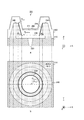
- FIG. 3 is an example of a cross-sectional view and a top view of the central sub-pixel 201 according to the first embodiment of the present technology.
- a is an example of a cross-sectional view of the sub-pixel 201
- b in the figure is an example of a top view thereof.
- the sub-pixel 201 includes an interlayer film 210, a via 220, an anode 230, a reflector 240, an organic light emitting layer 250, and a cathode 260.
- the direction perpendicular to the display surface 105 provided with the sub-pixel 201 is defined as the "Z direction", and the horizontal direction parallel to the display surface 105 is defined as the "X direction”.
- the vertical direction perpendicular to the X and Z directions is defined as the "Y direction”.
- a is a cross-sectional view of the sub-pixel 201 seen from the Y direction
- b in the figure is a top view of the sub-pixel 201 seen from the Z direction.
- a via 220 is provided in the interlayer film 210.
- An anode 230 is provided above the interlayer film 210 with the direction toward the cathode 260 facing upward, and the anode 230 is connected to a pixel circuit (not shown) in the sub-pixel 201 via a via 220.
- a reflector 240 is formed around the anode 230.
- the refractive index of the reflector 240 is lower than that of the organic light emitting layer 250.
- the material of the reflector 240 for example, silicon oxide (SiO) is used.
- the reflector 240 is tapered (in other words, tapered) along the Z direction. Due to this taper, a mortar-shaped reflecting surface 241 is formed inside the reflector 240.
- the thick line on the surface of the reflector 240 in the figure indicates the reflection surface 241.
- an organic light emitting layer 250 is formed on the anode 230 and the reflector 240.
- the structure of the organic light emitting layer 250 is generally a laminated structure of a charge injection layer, a charge transport layer, a light emitting layer, an electron transport layer, and an electron injection layer.
- a cathode 260 is provided above the organic light emitting layer 250.
- the cathode 260 is generally a metal thin film such as magnesium or silver, or a transparent electrode such as IZO (Indium Zinc Oxide).
- a protective film, a sealing resin, glass, and the like are further formed on the upper portion of the cathode 260, but these are omitted in the figure.
- Anode 230 and cathode 260 apply a voltage to the organic light emitting layer 250.
- the light emitting portion 251 which is a portion of the organic light emitting layer 250 sandwiched between the anode 230 and the cathode 260 emits light when the applied voltage fluctuates.
- the light from the light emitting unit 251 is totally reflected at the interface (that is, the reflecting surface 241) between the light emitting unit 251 and the reflector 240 having a low refractive index.
- the contact point between the anode 230 and the reflecting surface 241 is referred to as a reflector bottom R bottom, and the set of the reflector bottom R bottom is referred to as a “lower contour line”.
- the point on the reflection surface 241 farthest from the anode 230 is referred to as the reflector top R top, and the set of the reflector top R top is referred to as the “upper contour line”.
- the thick outer line of b indicates the upper contour line
- the thick inner line indicates the lower contour line.
- the upper contour line and the lower contour line are circular, but are not limited to circular and may be ellipse or the like.
- the angle formed by the left reflecting surface 241 and the anode 230 when viewed from a predetermined direction parallel to the display surface 105 is defined as a taper angle ⁇ L
- the angle formed by the right reflecting surface 241 and the anode 230 is defined as the taper angle ⁇ L.
- the taper angle ⁇ L on the left side and the taper angle ⁇ L on the right side can be seen from any direction as long as the sub-pixel 201 in the center is parallel to the display surface 105 (X direction, Y direction, etc.). It is substantially the same as the taper angle ⁇ R of .
- substantially matching means that the two values are exactly the same, or that the difference between them is within a predetermined allowable value.
- the central reflector 240 can reflect the light from the light emitting unit 251 in the Z direction.
- the light emitted by the organic light emitting layer 250 of each of the three sub-pixels 201 in the pixel 200 is, for example, R, G, and B.
- the color of the light emitted by the organic light emitting layer 250 can be changed by changing the organic molecules in the layer. Since the organic light emitting layer 250 emits R, G, and B light, a color image can be displayed without a color filter. As will be described later, a color filter may be provided on the sub-pixel 201.
- FIG. 4 is an example of a cross-sectional view and a top view of the sub-pixel 201 at the left end of the display surface 105 when viewed from the Z direction in the first embodiment of the present technology.
- a is an example of a cross-sectional view of the sub-pixel 201
- b in the figure is an example of a top view thereof.
- the leftmost sub-pixel 201 also includes an interlayer film 210, a via 220, an anode 230, a reflector 240, an organic light emitting layer 250, and a cathode 260, similarly to the central sub-pixel 201.
- the taper angle ⁇ L on the left side is larger than the taper angle ⁇ R on the right side. Therefore, as illustrated in b in the figure, the center of gravity C top of the upper contour line does not coincide with the center of gravity C bottom of the lower contour line, and the center of gravity C top shifts to the right. Due to the structure of the left-right asymmetric reflector 240, the leftmost reflector 240 can reflect the light from the light emitting unit 251 toward the central axis of the display surface 105.
- FIG. 5 is an example of a cross-sectional view and a top view of the sub-pixel 201 at the right end of the display surface 105 when viewed from the Z direction in the first embodiment of the present technology.
- a is an example of a cross-sectional view of the sub-pixel 201
- b in the figure is an example of a top view thereof.
- the rightmost sub-pixel 201 also includes an interlayer film 210, a via 220, an anode 230, a reflector 240, an organic light emitting layer 250, and a cathode 260, similarly to the central sub-pixel 201.
- the taper angle ⁇ L on the left side is smaller than the taper angle ⁇ R on the right side. Therefore, as illustrated in b in the figure, the center of gravity C top of the upper contour line does not coincide with the center of gravity C bottom of the lower contour line, and the center of gravity C top shifts to the left side. Due to the structure of the left-right asymmetric reflector 240, the rightmost reflector 240 can reflect the light from the light emitting unit 251 toward the central axis of the display surface 105.
- FIG. 6 is an example of a top view of the pixel array unit 130 according to the first embodiment of the present technology.
- the number of rows of the pixel array unit 130 is I (I is an integer), and the number of columns is J (J is an integer).
- the center of the display surface 105 on which the sub-pixels 201 are arranged is defined as a C array .
- the sub-pixel 201 at the address (I / 2, J / 2) has the center of gravity of the upper contour line (thick outer line) and the center of gravity of the lower contour line (thick inner line) as illustrated in the figure. Is almost the same.
- the distance between the center of gravity of the upper contour line and the center of gravity of the lower contour line becomes wider, and the center of gravity of the upper contour line shifts toward the center C array .
- the center of gravity of the upper contour line shifts toward the lower right.
- the center of gravity of the upper contour line shifts downward.
- the center of gravity of the upper contour line shifts in the lower left direction.
- the center of gravity of the upper contour line shifts to the right.
- the center of gravity of the upper contour line shifts to the left.
- the center of gravity of the upper contour line shifts toward the upper right.
- the center of gravity of the upper contour line shifts upward.
- the center of gravity of the upper contour line shifts toward the upper left.
- each reflector 240 of the sub-pixel 201 can reflect the light from the light emitting unit 251 toward the central axis passing through the central C array .
- FIG. 7 is a diagram for explaining the reflection direction of the reflector 240 in the first embodiment of the present technology.
- the alternate long and short dash line in the figure indicates the central axis of the display surface. The viewer shall view the image displayed on the display surface from the line-of-sight direction along the central axis.
- a light emitting unit 251 and a reflector 240 are provided for each of the plurality of sub-pixels 201 arranged on the display surface.
- the reflector 240 of the sub-pixel 201 in the center of the display surface reflects the light emitted by the light emitting unit 251 in the direction perpendicular to the display surface.
- the reflector 240 of the sub-pixel 201 on the left side reflects the light emitted by the light emitting unit 251 toward the right.
- the reflector 240 of the sub-pixel 201 on the right side reflects the light emitted by the light emitting unit 251 toward the left.
- the angle of the reflected light with respect to the display surface substantially coincides with 90 degrees in the sub-pixel 201 in the center, and the difference between the angle and 90 degrees increases as the distance from the center increases.
- the reflector 240 of any of the sub-pixels 201 on the display surface can reflect the light emitted by the light emitting unit in the direction toward the central axis (dashed line) of the display surface.
- FIG. 8 is a diagram for explaining the reflection direction of the reflector in the comparative example.
- the reflector 240 of the sub-pixel at any position on the display surface has the same taper angle, and each reflector 240 transmits the light emitted by the light emitting unit in the Z direction perpendicular to the display surface. Reflect toward.
- the light of the sub-pixel near the center is reflected toward the viewer, but the light of the sub-pixel located away from the center is not reflected toward the viewer.
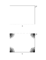
- FIG. 9 is a diagram showing an example of an image visually observed by the viewer in the first embodiment of the present technology and the comparative example.
- a is a diagram showing an example of an image 501 in which a viewer visually observes the display device 120 of the first embodiment.
- FIG. B in the figure is a diagram showing an example of an image 502 in which a viewer visually observes a display device of a comparative example.
- the image actually displayed by the display device is, for example, an image in which all pixels are white.
- the images 501 and 502 in the figure are not the images themselves actually displayed on the display device, but the images that are visible to the viewer when viewed.
- the taper angle of the reflector 240 is optimized for each pixel, the image 501 visually viewed by the viewer does not have uneven brightness. This is because the light of the light emitting unit 251 is reflected by the reflector 240 toward the viewer in any of the sub-pixels 201 of the display surface.
- the taper angle of the reflector 240 is the same for all the pixels, the brightness of the end portion (upper left, upper right, etc.) of the image 502 viewed by the viewer is reduced. , Brightness unevenness occurs. This is because the light of the sub-pixel near the center is reflected toward the viewer, but the light of the sub-pixel located far from the center is not reflected toward the viewer.
- FIG. 10 is a diagram for explaining a procedure up to gray tone exposure in the first embodiment of the present technology.
- FIG. A in the figure is a diagram for explaining a procedure of applying a resist and prebaking.
- Reference numeral b in the figure is a diagram for explaining a procedure of gray tone exposure.
- a low refractive index material 302 having a refractive index lower than that of the organic light emitting layer 250 is laminated on an interlayer film 210 on which a via 220 or the like is formed. Then, in the manufacturing system, the resist 301 is applied to the low refractive index material 302 by using a spin coating method or the like, and prebaking is performed by heating a hot plate or the like.
- the manufacturing system performs gray tone exposure.
- the gray tone mask 304 attached to the glass 303 is used.
- the gray tone mask 304 is provided with a slit pattern equal to or lower than the resolution of the exposure machine, and the slit pattern portion blocks a part of the light, so that the manufacturing system can realize an intermediate exposure.
- the degree of intermediate exposure can also be adjusted by adjusting the width and density of the slits.
- a general i-line resist or one for KrF resist is used as the resist 301 according to the wavelength of the exposure machine.
- the manufacturing system can adjust the taper angle by adjusting the width and density of the slits of the gray tone mask 304 in the gray tone exposure.
- the gray tone mask 304 is not opened, and the resist 301 immediately below this is not exposed.
- intermediate exposure is performed on the resist 301 directly under X1 to X2, and the exposure amount gradually increases from X1 to X2.
- the resist 301 after development can be tapered.
- the gray tone mask 304 is opened in the portions X2 to X3, and the resist 301 immediately below this is exposed.
- the thick dotted line in the figure shows the shape of the resist 301 after development, which will be described later.
- FIG. 11 is a diagram for explaining the procedure up to dry etching in the first embodiment of the present technology.
- a is a diagram for explaining the procedure of development and post-baking.
- Reference numeral b in the figure is a diagram for explaining a dry etching procedure.
- the manufacturing system removes the photosensitive portion of the resist 301 with a predetermined developer.
- the developed resist 301 has a mortar-shaped wall surface.
- the group of points on the wall surface farthest from the low refractive index material 302 is defined as the upper contour line
- the group of contacts between the low refractive index material 302 and the wall surface is defined as the lower contour line.
- the distance between the center of gravity of the upper contour line and the center of gravity of the lower contour line increases as the distance from the central axis of the display surface increases.
- post-baking such as by hot plate heating.
- the manufacturing system transfers the pattern of the developed resist 301 to the low refractive index material 302 by performing dry etching on the low refractive index material 302.
- dry etching the low refractive index material 302 is also tapered along the tapered shape of the resist 301, and the reflector 240 made of the low refractive index material 302 is formed.
- FIG. 12 is a diagram for explaining the procedure up to pretreatment and vapor deposition in the first embodiment of the present technology.
- a in the figure is a diagram for explaining a procedure for peeling the resist 301.
- Reference numeral b in the figure is a diagram for explaining the procedure of pretreatment and thin film deposition.
- the manufacturing system removes (ashing) the resist by plasma treatment such as oxygen (O 2 ), and performs alkaline chemical treatment (that is, wet treatment) on a small amount of residue. Remove completely.
- plasma treatment such as oxygen (O 2 )
- alkaline chemical treatment that is, wet treatment
- the manufacturing system performs pretreatment using O 2 plasma to form the organic light emitting layer 250 and the cathode 260.
- the organic light emitting layer 250 is generally formed by thin film deposition or coating
- the cathode 260 is generally formed by thin film deposition or sputtering.
- FIG. 13 is a diagram for explaining a procedure up to sealing in the first embodiment of the present technology.
- FIG. A in the figure is a diagram for explaining a procedure for forming a protective film.
- Reference numeral b in the figure is a diagram for explaining a sealing procedure.
- the manufacturing system forms the protective film 305 by using CVD (Chemical Vapor Deposition) or the like. Since the OLED is sensitive to moisture, it is protected by the protective film 305. Silicon nitride (SiN) or the like is generally used as the protective film 305.
- the manufacturing system encloses the sealing resin 306 and attaches it to the glass 307.
- FIG. 14 is a flowchart showing an example of a manufacturing method of the display device 120 according to the first embodiment of the present technology.
- the low refractive index material 302 is laminated on the interlayer film 210, and resist is applied and prebaked (step S901). Then, the manufacturing system performs gray tone exposure (step S902), develops and post-bakes (step S903).
- step S904 the manufacturing system performs dry etching (step S904) and peels off the resist (step S905).
- the manufacturing system performs pretreatment and thin film deposition (step S906) to form a protective film (step S907).
- step S908 the manufacturing system seals with glass or the like (step S908), and ends the operation for manufacturing the display device 120.
- the reflector 240 reflects the light of the light emitting unit 251 toward the central axis of the display surface 105, the viewer is viewed along the central axis. It is possible to suppress uneven brightness of the image visually observed by. Thereby, the image quality of the image can be improved.
- each of the organic light emitting layers 250 of the plurality of sub-pixels 201 self-lumines R, G, and B light.
- the display device 120 of the second embodiment is different from the first embodiment in that a color filter is further provided on the sub-pixel 201.
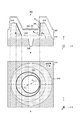
- FIG. 15 is an example of a cross-sectional view and a top view of the central sub-pixel 201 in the second embodiment of the present technology.
- a is an example of a cross-sectional view of the sub-pixel 201
- b in the figure is an example of a top view thereof.
- the sub-pixel 201 of the second embodiment is different from the first embodiment in that a color filter 270 is further provided.
- the color filter 270 transmits visible light of a predetermined color (any of R, G, B, etc.).
- the light emitted by the light emitting unit 251 and the light reflected by the reflector 240 pass through the color filter 270 and are output from the display device 120.
- each color filter 270 of the plurality of sub-pixels 201 in the pixel 200 transmits different colors (R, G, B, etc.). By arranging these color filters 270, the display device 120 can display a color image. Further, by arranging the color filter 270, the self-luminous color can be only white, so that it is not necessary to change the organic molecule for each color. As a result, the cost can be reduced as compared with the first embodiment in which the color filter 270 is not provided.
- the thick line b in the figure indicates the four sides of the color filter 270. As illustrated in b in the figure, in the central sub-pixel 201, the center of gravity of the color filter 270 substantially coincides with the center of gravity of the sub-pixel 201.
- FIG. 16 is an example of a cross-sectional view and a top view of the leftmost sub-pixel 201 in the second embodiment of the present technology.
- a is an example of a cross-sectional view of the sub-pixel 201
- b in the figure is an example of a top view thereof.
- a color filter 270 is also provided in the leftmost sub-pixel 201.
- the center of gravity of the color filter 270 is shifted to the right, unlike the center of gravity of the sub-pixel 201.
- the center of gravity of the color filter 270 shifts to the left.
- the center of gravity of the color filter 270 shifts toward the central axis for the other sub-pixels 201 other than the center. The distance between the center of gravity of the color filter 270 and the center of gravity of the sub-pixel 201 becomes wider as the distance from the central axis of the display surface increases.
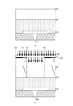
- FIG. 17 is an example of a top view of the left end and center sub-pixels 201 in the second embodiment of the present technology.
- a is an example of a top view of the three sub-pixels 201 in the pixel 200 arranged at the left end.
- b is an example of a top view of the three sub-pixels 201 in the pixel 200 arranged in the center.
- the center of gravity of the color filter 270 in each of the three central sub-pixels 201 substantially coincides with the center of gravity of the sub-pixel 201.
- the color filter 270 at the address (I / 2, 0) near the center transmits light of R, for example, and the color filter 270 at the address (I / 2, 1) next to it transmits light of G, for example. To do.
- the color filter 270 at the address (I / 2, 2) next to it transmits, for example, the light of B.
- the center of gravity of the color filter 270 shifts to the left side unlike the center of gravity of the sub-pixel 201. Further, the distance between the center of gravity of the color filter 270 and the center of gravity of the sub-pixel 201 becomes wider as the distance from the central axis increases. The same applies to the sub-pixel 201 of another address such as the right end.
- the center of gravity of the color filter 270 in the central pixel 200 substantially coincides with the center of gravity of the sub-pixel 201.
- the viewing angle for each color can be widened by shifting the center of gravity of the color filter 270 according to the distance from the central axis of the display surface.
- the distance between the center of gravity of the color filter 270 and the center of gravity of the sub-pixel 201 is widened as the distance from the central axis increases, so that the viewing angle for each color is widened. Can be widened. Further, by arranging the color filter 270, the self-luminous color can be only white, so that it is not necessary to change the organic molecules in the organic light emitting layer 250 for each color. As a result, it is possible to avoid complication of the manufacturing process of the organic light emitting layer 250 as compared with the first embodiment in which the color filter 270 is not provided.
- the technology according to the present disclosure can be applied to various products.
- the technology according to the present disclosure is realized as a device mounted on a moving body of any kind such as an automobile, an electric vehicle, a hybrid electric vehicle, a motorcycle, a bicycle, a personal mobility, an airplane, a drone, a ship, and a robot. You may.
- FIG. 18 is a block diagram showing a schematic configuration example of a vehicle control system, which is an example of a moving body control system to which the technique according to the present disclosure can be applied.
- the vehicle control system 12000 includes a plurality of electronic control units connected via the communication network 12001.
- the vehicle control system 12000 includes a drive system control unit 12010, a body system control unit 12020, an outside information detection unit 12030, an in-vehicle information detection unit 12040, and an integrated control unit 12050.
- a microcomputer 12051, an audio image output unit 12052, and an in-vehicle network I / F (interface) 12053 are shown as a functional configuration of the integrated control unit 12050.
- the drive system control unit 12010 controls the operation of the device related to the drive system of the vehicle according to various programs.
- the drive system control unit 12010 provides a driving force generator for generating the driving force of the vehicle such as an internal combustion engine or a driving motor, a driving force transmission mechanism for transmitting the driving force to the wheels, and a steering angle of the vehicle. It functions as a control device such as a steering mechanism for adjusting and a braking device for generating braking force of the vehicle.
- the body system control unit 12020 controls the operation of various devices mounted on the vehicle body according to various programs.
- the body system control unit 12020 functions as a keyless entry system, a smart key system, a power window device, or a control device for various lamps such as headlamps, back lamps, brake lamps, blinkers or fog lamps.
- the body system control unit 12020 may be input with radio waves transmitted from a portable device that substitutes for the key or signals of various switches.
- the body system control unit 12020 receives inputs of these radio waves or signals and controls a vehicle door lock device, a power window device, a lamp, and the like.
- the vehicle outside information detection unit 12030 detects information outside the vehicle equipped with the vehicle control system 12000.
- an imaging unit 12031 is connected to the vehicle exterior information detection unit 12030.
- the vehicle outside information detection unit 12030 causes the image pickup unit 12031 to capture an image of the outside of the vehicle and receives the captured image.
- the vehicle exterior information detection unit 12030 may perform object detection processing or distance detection processing such as a person, a vehicle, an obstacle, a sign, or characters on the road surface based on the received image.
- the imaging unit 12031 is an optical sensor that receives light and outputs an electric signal according to the amount of the light received.
- the image pickup unit 12031 can output an electric signal as an image or can output it as distance measurement information. Further, the light received by the imaging unit 12031 may be visible light or invisible light such as infrared light.
- the in-vehicle information detection unit 12040 detects the in-vehicle information.
- a driver state detection unit 12041 that detects the driver's state is connected to the in-vehicle information detection unit 12040.
- the driver state detection unit 12041 includes, for example, a camera that images the driver, and the in-vehicle information detection unit 12040 determines the degree of fatigue or concentration of the driver based on the detection information input from the driver state detection unit 12041. It may be calculated, or it may be determined whether the driver is dozing.
- the microcomputer 12051 calculates the control target value of the driving force generator, the steering mechanism, or the braking device based on the information inside and outside the vehicle acquired by the vehicle exterior information detection unit 12030 or the vehicle interior information detection unit 12040, and the drive system control unit.
- a control command can be output to 12010.
- the microcomputer 12051 realizes ADAS (Advanced Driver Assistance System) functions including vehicle collision avoidance or impact mitigation, follow-up driving based on inter-vehicle distance, vehicle speed maintenance driving, vehicle collision warning, vehicle lane deviation warning, and the like. It is possible to perform cooperative control for the purpose of.
- ADAS Advanced Driver Assistance System
- the microcomputer 12051 controls the driving force generator, the steering mechanism, the braking device, and the like based on the information around the vehicle acquired by the vehicle exterior information detection unit 12030 or the vehicle interior information detection unit 12040. It is possible to perform coordinated control for the purpose of automatic driving that runs autonomously without depending on the operation.
- the microcomputer 12051 can output a control command to the body system control unit 12020 based on the information outside the vehicle acquired by the vehicle exterior information detection unit 12030.
- the microcomputer 12051 controls the headlamps according to the position of the preceding vehicle or the oncoming vehicle detected by the external information detection unit 12030, and performs cooperative control for the purpose of antiglare such as switching the high beam to the low beam. It can be carried out.
- the audio image output unit 12052 transmits the output signal of at least one of the audio and the image to the output device capable of visually or audibly notifying the passenger of the vehicle or the outside of the vehicle.
- an audio speaker 12061, a display unit 12062, and an instrument panel 12063 are exemplified as output devices.
- the display unit 12062 may include, for example, at least one of an onboard display and a heads-up display.
- FIG. 19 is a diagram showing an example of the installation position of the imaging unit 12031.
- the imaging units 12101, 12102, 12103, 12104, 12105 are provided.
- the imaging units 12101, 12102, 12103, 12104, 12105 are provided at positions such as, for example, the front nose, side mirrors, rear bumpers, back doors, and the upper part of the windshield in the vehicle interior of the vehicle 12100.
- the imaging unit 12101 provided on the front nose and the imaging unit 12105 provided on the upper part of the windshield in the vehicle interior mainly acquire an image in front of the vehicle 12100.
- the imaging units 12102 and 12103 provided in the side mirrors mainly acquire images of the side of the vehicle 12100.
- the imaging unit 12104 provided on the rear bumper or the back door mainly acquires an image of the rear of the vehicle 12100.
- the imaging unit 12105 provided on the upper part of the windshield in the vehicle interior is mainly used for detecting a preceding vehicle, a pedestrian, an obstacle, a traffic light, a traffic sign, a lane, or the like.
- FIG. 19 shows an example of the photographing range of the imaging units 12101 to 12104.
- the imaging range 12111 indicates the imaging range of the imaging unit 12101 provided on the front nose
- the imaging ranges 12112 and 12113 indicate the imaging ranges of the imaging units 12102 and 12103 provided on the side mirrors, respectively
- the imaging range 12114 indicates the imaging range of the imaging units 12102 and 12103.
- the imaging range of the imaging unit 12104 provided on the rear bumper or the back door is shown. For example, by superimposing the image data captured by the imaging units 12101 to 12104, a bird's-eye view image of the vehicle 12100 as viewed from above can be obtained.
- At least one of the imaging units 12101 to 12104 may have a function of acquiring distance information.
- at least one of the image pickup units 12101 to 12104 may be a stereo camera composed of a plurality of image pickup elements, or may be an image pickup element having pixels for phase difference detection.
- the microcomputer 12051 has a distance to each three-dimensional object within the imaging range 12111 to 12114 based on the distance information obtained from the imaging units 12101 to 12104, and a temporal change of this distance (relative velocity with respect to the vehicle 12100).
- a predetermined speed for example, 0 km / h or more.
- the microcomputer 12051 can set an inter-vehicle distance to be secured in front of the preceding vehicle in advance, and can perform automatic braking control (including follow-up stop control), automatic acceleration control (including follow-up start control), and the like. In this way, it is possible to perform coordinated control for the purpose of automatic driving or the like in which the vehicle travels autonomously without depending on the operation of the driver.
- the microcomputer 12051 converts three-dimensional object data related to a three-dimensional object into two-wheeled vehicles, ordinary vehicles, large vehicles, pedestrians, utility poles, and other three-dimensional objects based on the distance information obtained from the imaging units 12101 to 12104. It can be classified and extracted and used for automatic avoidance of obstacles. For example, the microcomputer 12051 distinguishes obstacles around the vehicle 12100 into obstacles that can be seen by the driver of the vehicle 12100 and obstacles that are difficult to see. Then, the microcomputer 12051 determines the collision risk indicating the risk of collision with each obstacle, and when the collision risk is equal to or higher than the set value and there is a possibility of collision, the microcomputer 12051 via the audio speaker 12061 or the display unit 12062. By outputting an alarm to the driver and performing forced deceleration and avoidance steering via the drive system control unit 12010, driving support for collision avoidance can be provided.
- At least one of the imaging units 12101 to 12104 may be an infrared camera that detects infrared rays.
- the microcomputer 12051 can recognize a pedestrian by determining whether or not a pedestrian is present in the captured image of the imaging units 12101 to 12104.
- pedestrian recognition includes, for example, a procedure for extracting feature points in an image captured by an imaging unit 12101 to 12104 as an infrared camera, and pattern matching processing for a series of feature points indicating the outline of an object to determine whether or not the pedestrian is a pedestrian. It is done by the procedure to determine.
- the audio image output unit 12052 When the microcomputer 12051 determines that a pedestrian is present in the captured images of the imaging units 12101 to 12104 and recognizes the pedestrian, the audio image output unit 12052 outputs a square contour line for emphasizing the recognized pedestrian.
- the display unit 12062 is controlled so as to superimpose and display. Further, the audio image output unit 12052 may control the display unit 12062 so as to display an icon or the like indicating a pedestrian at a desired position.
- the above is an example of a vehicle control system to which the technology according to the present disclosure can be applied.
- the technique according to the present disclosure can be applied to the display unit 12062 among the configurations described above.
- the display device 120 of FIG. 2 can be applied to the display unit 12062.
- the present technology can have the following configurations.
- a pixel array in which a plurality of sub-pixels each provided with a light emitting unit and a reflector for reflecting light emitted by the light emitting unit toward the central axis of a predetermined display surface are arranged on the display surface.
- a display device including a unit.
- Each of the plurality of sub-pixels is further provided with an anode and a cathode for applying a voltage to the light emitting portion.
- the reflector is formed around the anode and
- the reflector has a mortar-shaped reflecting surface and has a mortar-shaped reflecting surface.
- the distance between the center of gravity of the upper contour line, which is a collection of points on the reflection surface farthest from the anode, and the center of gravity of the lower contour line, which is a collection of contacts between the anode and the reflection surface, is the distance from the central axis to the light emitting portion.
- the display device according to (1) or (2) above which is wider as the distance to is longer.
- a pixel array in which a plurality of sub-pixels each provided with a light emitting unit and a reflector for reflecting light emitted by the light emitting unit toward the central axis of a predetermined display surface are arranged on the display surface.
- Department and An electronic device including a driver for driving each of the plurality of sub-pixels.
- the resist from which the photosensitive portion has been removed has a mortar-shaped wall surface.
- the distance between the center of gravity of the upper contour line, which is a collection of points on the wall surface farthest from the low refractive index material, and the center of gravity of the lower contour line, which is a collection of contacts of the low refractive index material and the wall surface, is indicated by a predetermined value.
- Display unit 100 Electronic equipment 105 Display surface 110 Battery 120 Display device 121 Control circuit 122 H driver 123 V driver 130 Pixel array part 200 pixels 201 Sub-pixel 210 Interlayer film 220 Via 230 Anode 240 Reflector 241 Reflective surface 250 Organic light emitting layer 251 Light emitting part 260 Cathode 270 Color filter 301 Resist 302 Low refractive index material 303, 307 Glass 304 Gray tone mask 305 Protective film 306 Encapsulating resin 12062 Display unit
Landscapes
- Engineering & Computer Science (AREA)
- Physics & Mathematics (AREA)
- General Physics & Mathematics (AREA)
- Theoretical Computer Science (AREA)
- Microelectronics & Electronic Packaging (AREA)
- Manufacturing & Machinery (AREA)
- Optics & Photonics (AREA)
- Electroluminescent Light Sources (AREA)
Abstract
OLEDを設けた表示装置において、画像の画質を向上させる。 表示装置は、画素アレイ部を具備する。その画素アレイ部の表示面は、複数の副画素が配列される。また、その表示装置の具備する画素アレイ部において複数の副画素のそれぞれには、発光部とリフレクタとが設けられる。また、表示装置の具備する画素アレイ部に配列された複数の副画素のそれぞれにおいて、リフレクタは、表示面の中心軸への方向に向けて発光部の発する光を反射する。
Description
本技術は、表示装置に関する。詳しくは、自発光素子を用いる表示装置、電子機器および表示装置の製造方法に関する。
従来より、様々な表示装置において、低消費電力化および薄膜化が可能なことや、応答速度が速いことなどの特徴を考慮して、OLED(Organic Light Emitting Diode)が用いられている。例えば、R(Red)、G(Green)およびB(Blue)などのカラーフィルタと、OLEDとを画素毎に配置した表示装置が提案されている(例えば、特許文献1参照。)。
上述の従来技術では、OLEDからの主光線の光学的距離をR、GおよびBの色毎に調整することによって、それぞれの色の波長を適切な値に設定している。しかしながら、上述の表示装置では、表示装置の中心からの距離に関わらず、主光線の方向は、全ての画素で、表示面に対して垂直な方向に設定されている。このため、表示装置の端部からの主光線が視聴者の眼に届きにくくなるおそれがある。これにより、視聴者が目視した画像に輝度ムラが生じ、その画質が低下するという問題がある。
本技術はこのような状況に鑑みて生み出されたものであり、OLEDを設けた表示装置において、画像の画質を向上させることを目的とする。
本技術は、上述の問題点を解消するためになされたものであり、その第1の側面は、発光部と、所定の表示面の中心軸への方向に向けて上記発光部の発する光を反射するリフレクタとがそれぞれに設けられた複数の副画素を上記表示面に配列した画素アレイ部を具備する表示装置である。これにより、複数の副画素のそれぞれからの光が、中心軸上の視聴者に届けられるという作用をもたらす。
また、この第1の側面において、上記リフレクタによる反射光の上記表示面に対する角度と90度との差は、上記中心軸からの距離が遠いほど小さくなってもよい。これにより、リフレクタによって、視聴者の方へ光が反射されるという作用をもたらす。
また、この第1の側面において、上記複数の副画素のそれぞれには、上記発光部に電圧を印加するアノードおよびカソードがさらに設けられ、上記リフレクタは、上記アノードの周囲に形成され、上記リフレクタは、すり鉢状の反射面を有し、上記アノードから最も遠い上記反射面上の点の集まりである上部等高線の重心と上記アノードおよび上記反射面の接点の集まりである下部等高線の重心との間の間隔は、上記中心軸から上記発光部までの距離が遠いほど広くてもよい。これにより、リフレクタのすり鉢状の反射面によって、視聴者の方へ光が反射されるという作用をもたらす。
また、この第1の側面において、上記複数の副画素のそれぞれには、所定の色の可視光を透過するカラーフィルタがさらに設けられてもよい。これにより、カラー画像が表示されるという作用をもたらす。
また、この第1の側面において、上記カラーフィルタの重心と副画素の重心との間の間隔は、上記中心軸から上記副画素までの距離が遠いほど広くてもよい。これにより、色ごとの視野角が広くなるという作用をもたらす。
また、本技術の第2の側面は、発光部と、所定の表示面の中心軸への方向に向けて上記発光部の発する光を反射するリフレクタとがそれぞれに設けられた複数の副画素を上記表示面に配列した画素アレイ部と、上記複数の副画素のそれぞれを駆動するドライバとを具備する電子機器である。これにより、ドライバにより駆動された複数の副画素のそれぞれからの光が、中心軸上の視聴者に届けられるという作用をもたらす。
また、本技術の第3の側面は、屈折率が所定の有機発光層より低い所定の低屈折率材料に所定のレジストを塗布する塗布手順と、上記レジストをグレートーン露光により感光する露光手順と、上記レジストの感光部分を所定の現像液により除去する現像手順と、上記低屈折率材料に対してエッチングを行うことにより上記感光部分が除去された上記レジストのパターンを上記低屈折率材料に転写するエッチング手順とを具備する表示装置の製造方法である。これにより、複数の副画素のそれぞれからの光が視聴者に届く表示装置が製造されるという作用をもたらす。
また、この第3の側面において、上記感光部分が除去された上記レジストは、すり鉢状の壁面を有し、上記低屈折率材料から最も遠い上記壁面上の点の集まりである上部等高線の重心と上記低屈折率材料および上記壁面の接点の集まりである下部等高線の重心との間の間隔は、所定の表示面の中心軸からの距離が遠いほど広くてもよい。これにより、視聴者の方へ光を反射するリフレクタが形成されるという作用をもたらす。
以下、本技術を実施するための形態(以下、実施の形態と称する)について説明する。説明は以下の順序により行う。
1.第1の実施の形態(表示面の中心軸の方へ反射させる例)
2.第2の実施の形態(カラーフィルタを設け、表示面の中心軸の方へ反射させる例)
3.移動体への応用例
1.第1の実施の形態(表示面の中心軸の方へ反射させる例)
2.第2の実施の形態(カラーフィルタを設け、表示面の中心軸の方へ反射させる例)
3.移動体への応用例
<1.第1の実施の形態>
[電子機器の構成例]
図1は、本技術の第1の実施の形態における電子機器100の外観図の一例である。この電子機器100は、画像などの様々な情報を表示することができる機器であり、それらの情報を表示するための表示面105を備える。電子機器100としては、スマートフォンなどのモバイル機器や、VR(Virtual Reality)端末などが想定される。
[電子機器の構成例]
図1は、本技術の第1の実施の形態における電子機器100の外観図の一例である。この電子機器100は、画像などの様々な情報を表示することができる機器であり、それらの情報を表示するための表示面105を備える。電子機器100としては、スマートフォンなどのモバイル機器や、VR(Virtual Reality)端末などが想定される。
表示面105の中心を通り、表示面105に垂直な軸を以下、「中心軸」と称する。同図における一点鎖線は、中心軸を示す。表示面105の表示する画像を視聴者が目視する際の視線方向は、主として、表示面105の中心軸に沿った方向であることが想定される。
図2は、本技術の第1の実施の形態における電子機器100の一構成例を示すブロック図である。この電子機器100は、表示装置120およびバッテリ110を備える。なお、電子機器100がVR端末である場合、広角レンズを含む光学系がさらに配置される。
バッテリ110は、放電により表示装置120に電力を供給するものである。バッテリ110として、例えば、放電に加えて充電を行うこともできる二次電池が用いられる。二次電池として、例えば、リチウムイオン電池が用いられる。
表示装置120は、制御回路121、Hドライバ122、Vドライバ123および画素アレイ部130を備える。画素アレイ部130は、表示面105を有し、その表示面105には、二次元格子状に複数の画素200が配列される。画素200のそれぞれは、互いに異なる色の光を発する複数の副画素201を含む。例えば、画素200ごとに、R、GおよびBの光を発する3つの副画素201が配置される。なお、同図において、副画素201の形状は正方形であるが、この形状に限定されず、長方形などであってもよい。
以下、所定の水平方向に配列された副画素201の集合を「行」と称し、行に垂直な方向に配列された副画素201の集合を「列」と称する。
制御回路121は、画像データに基づいてHドライバ122およびVドライバ123のそれぞれの駆動タイミングを制御するものである。Hドライバ122は、副画素201を列単位で駆動するものである。Vドライバ123は、副画素201を行単位で駆動するものである。なお、Hドライバ122およびVドライバ123は、特許請求の範囲に記載のドライバの一例である。
[画素の構成例]
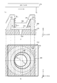
図3は、本技術の第1の実施の形態における中央の副画素201の断面図および上面図の一例である。同図におけるaは、副画素201の断面図の一例であり、同図におけるbは、その上面図の一例である。この副画素201は、層間膜210、ビア220、アノード230、リフレクタ240、有機発光層250およびカソード260を備える。
図3は、本技術の第1の実施の形態における中央の副画素201の断面図および上面図の一例である。同図におけるaは、副画素201の断面図の一例であり、同図におけるbは、その上面図の一例である。この副画素201は、層間膜210、ビア220、アノード230、リフレクタ240、有機発光層250およびカソード260を備える。
また、副画素201の設けられた表示面105に垂直な方向を「Z方向」とし、表示面105に平行な水平方向を「X方向」とする。X方向およびZ方向に垂直な垂直方向を「Y方向」とする。同図におけるaは、Y方向から見た副画素201の断面図であり、同図におけるbは、Z方向から見た副画素201の上面図である。
同図におけるaに例示するように、層間膜210内にはビア220が設けられる。カソード260への方向を上方向として、層間膜210の上部にはアノード230が設けられ、そのアノード230はビア220を介して、副画素201内の画素回路(不図示)と接続される。
また、アノード230の周囲には、リフレクタ240が形成される。このリフレクタ240の屈折率は、有機発光層250よりも低い。リフレクタ240の材料として、例えば、酸化シリコン(SiO)が用いられる。また、リフレクタ240は、Z方向に沿って先細りになって(言い換えれば、テーパーがつけられて)いる。このテーパーにより、リフレクタ240の内側には、すり鉢状の反射面241が形成される。同図におけるリフレクタ240の表面の太線は、反射面241を示す。
また、アノード230およびリフレクタ240の上部には、有機発光層250が形成される。この有機発光層250の構造は、一般的には、電荷注入層、電荷輸送層、発光層、電子輸送層および電子注入層の積層構造である。有機発光層250の上部には、カソード260が設けられる。カソード260は、一般的には、マグネシウムや銀などの金属薄膜や、IZO(Indium Zinc Oxide)などの透明電極である。このカソード260の上部には、保護膜、封止樹脂やガラスなどがさらに形成されるが、同図において、これらは省略されている。
アノード230およびカソード260は、有機発光層250に電圧を印加する。有機発光層250のうち、アノード230およびカソード260に挟まれた部分である発光部251は、印加された電圧が変動する際に発光する。発光部251からの光は、その発光部251と屈折率の低いリフレクタ240との界面(すなわち、反射面241)において全反射される。
アノード230および反射面241の接点をリフレクタボトムRbottomとし、このリフレクタボトムRbottomの集合を「下部等高線」とする。一方、アノード230から最も遠い反射面241上の点をリフレクタトップRtopとし、このリフレクタトップRtopの集合を「上部等高線」とする。同図におけるbの外側の太線は、上部等高線を示し、内側の太線は、下部等高線を示す。なお、同図のbにおいて、上部等高線および下部等高線は円形であるが、円形に限定されず、楕円などであってもよい。
また、表示面105に平行な所定方向(Y方向など)から見て左側の反射面241とアノード230とがなす角度をテーパー角θLとし、右側の反射面241とアノード230とがなす角度をテーパー角θRとする。
同図におけるaに例示するように、中央の副画素201において表示面105に平行な方向(X方向やY方向など)であれば、どの方向から見ても、左側のテーパー角θLと右側のテーパー角θRとは略一致する。ここで、「略一致」とは、2つの値が完全一致すること、または、それらの差分が所定の許容値以内であることを意味する。
左側のテーパー角θLと右側のテーパー角θRとが略一致するため、同図におけるbに例示するように、下部等高線の重心Cbottomは、上部等高線の重心Ctopと略一致する。この左右対称なリフレクタ240の構造により、中央のリフレクタ240は、発光部251からの光を、Z方向に向けて反射させることができる。
ここで、画素200内の3つの副画素201のそれぞれの有機発光層250の発光する光は、例えば、R、GおよびBである。有機発光層250が発光する光の色は、その層内の有機分子を変えることにより変更することができる。有機発光層250がR、GおよびBの光を発することにより、カラーフィルタなしに、カラー画像を表示させることができる。なお、後述するように、副画素201にカラーフィルタを設けることもできる。
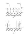
図4は、本技術の第1の実施の形態におけるZ方向から見て表示面105の左端の副画素201の断面図および上面図の一例である。同図におけるaは、副画素201の断面図の一例であり、同図におけるbは、その上面図の一例である。
左端の副画素201も、中央の副画素201と同様に、層間膜210、ビア220、アノード230、リフレクタ240、有機発光層250およびカソード260を備える。
ただし、同図におけるaに例示するように、左端の副画素201において、左側のテーパー角θLの方が、右側のテーパー角θRより大きい。このため、同図におけるbに例示するように、上部等高線の重心Ctopは、下部等高線の重心Cbottomと一致せず、重心Ctopは、右側にずれてしまう。この左右非対称なリフレクタ240の構造により、左端のリフレクタ240は、発光部251からの光を、表示面105の中心軸への方向に向けて反射させることができる。
図5は、本技術の第1の実施の形態におけるZ方向から見て表示面105の右端の副画素201の断面図および上面図の一例である。同図におけるaは、副画素201の断面図の一例であり、同図におけるbは、その上面図の一例である。
右端の副画素201も、中央の副画素201と同様に、層間膜210、ビア220、アノード230、リフレクタ240、有機発光層250およびカソード260を備える。
ただし、同図におけるaに例示するように、右端の副画素201において、左側のテーパー角θLの方が、右側のテーパー角θRより小さい。このため、同図におけるbに例示するように、上部等高線の重心Ctopは、下部等高線の重心Cbottomと一致せず、重心Ctopは、左側にずれてしまう。この左右非対称なリフレクタ240の構造により、右端のリフレクタ240は、発光部251からの光を、表示面105の中心軸への方向に向けて反射させることができる。
[画素アレイ部の構成例]
図6は、本技術の第1の実施の形態における画素アレイ部130の上面図の一例である。画素アレイ部130の行数をI(Iは、整数)とし、列数をJ(Jは、整数)とする。副画素201に割り当てられるアドレスを(i、j)とする。iは、0乃至I-1の整数であり、jは、0乃至J-1の整数である。
図6は、本技術の第1の実施の形態における画素アレイ部130の上面図の一例である。画素アレイ部130の行数をI(Iは、整数)とし、列数をJ(Jは、整数)とする。副画素201に割り当てられるアドレスを(i、j)とする。iは、0乃至I-1の整数であり、jは、0乃至J-1の整数である。
また、副画素201が配列される表示面105の中心をCarrayとする。この中心Carray付近、例えば、アドレス(I/2、J/2)の副画素201は、同図に例示するように上部等高線(外側の太線)の重心と下部等高線(内側の太線)の重心とが略一致する。
一方、中心Carrayから遠い副画素201ほど、上部等高線の重心と下部等高線の重心との間の間隔が広くなり、上部等高線の重心は、中心Carrayへの方向へずれる。
例えば、Z方向から見て左上のアドレス(0、0)の副画素201では、上部等高線(外側の太線)の重心が右下の方向へずれる。中央の上側のアドレス(0、J/2)の副画素201では、上部等高線の重心が下方向へずれる。右上のアドレス(0、J-1)の副画素201では、上部等高線の重心が左下の方向へずれる。中央の左側のアドレス(I/2、0)の副画素201では、上部等高線の重心が右方向へずれる。中央の右側のアドレス(I/2、J-1)の副画素201では、上部等高線の重心が左方向へずれる。左下のアドレス(I-1、0)の副画素201では、上部等高線の重心が右上の方向へずれる。中央の下側のアドレス(I-1、J/2)の副画素201では、上部等高線の重心が上方向へずれる。右下のアドレス(I-1、J-1)の副画素201では、上部等高線の重心が左上の方向へずれる。
上述の構成により、副画素201のそれぞれのリフレクタ240は、発光部251からの光を、中心Carrayを通る中心軸の方向に向けて反射することができる。
図7は、本技術の第1の実施の形態におけるリフレクタ240の反射方向を説明するための図である。同図における一点鎖線は、表示面の中心軸を示す。視聴者は、この中心軸に沿った視線方向から、表示面に表示された画像を視聴するものとする。
画素アレイ部130において、表示面に配列された複数の副画素201のそれぞれには、発光部251とリフレクタ240とが設けられる。
同図に例示するように、表示面の中央の副画素201のリフレクタ240は、発光部251の発した光を表示面に垂直な方向に反射する。Y方向から見て、左側の副画素201のリフレクタ240は、発光部251の発した光を右方向に向けて反射する。右側の副画素201のリフレクタ240は、発光部251の発した光を左方向に向けて反射する。反射光の表示面に対する角度は、中央の副画素201では、90度と略一致し、中央から離れるほど、その角度と90度との差が大きくなる。
上述の構成により、表示面上のいずれの副画素201においても、そのリフレクタ240は、表示面の中心軸(一点鎖線)への方向に向けて発光部の発する光を反射することができる。このようにリフレクタ240のテーパー角を画素毎に最適化することにより、表示面のどの位置の光も、視聴者の方向に向けることができる。
ここで、全ての副画素201についてリフレクタ240のテーパー角を同一にした一般的な構成を比較例として想定する。
図8は、比較例におけるリフレクタの反射方向を説明するための図である。同図に例示するように、表示面のどの位置の副画素のリフレクタ240も、そのテーパー角は同一であり、それぞれのリフレクタ240は、発光部の発した光を表示面に垂直なZ方向に向けて反射する。この比較例では、中央付近の副画素の光は視聴者の方に向けて反射されるが、中央から離れた位置の副画素の光は、視聴者の方に向けて反射されない。
図9は、本技術の第1の実施の形態と比較例とにおける視聴者が目視する画像の一例を示す図である。同図におけるaは、第1の実施の形態の表示装置120を視聴者が目視した画像501の一例を示す図である。同図におけるbは、比較例の表示装置を視聴者が目視した画像502の一例を示す図である。表示装置が実際に表示する画像は、例えば、全画素が白色の画像である。ただし、同図における画像501および502は、表示装置に実際に表示された画像そのものでなく、視聴した際に視聴者の目に写る画像である。
同図におけるaに例示するように、リフレクタ240のテーパー角を画素毎に最適化した場合、視聴者が目視する画像501に輝度ムラが生じない。これは、表示面のいずれの副画素201においても、発光部251の光がリフレクタ240により視聴者の方向に向けて反射されるためである。
一方、同図におけるbに例示するように、全ての画素についてリフレクタ240のテーパー角を同一にした比較例では、視聴者が目視する画像502の端部(左上や右上など)の輝度が低下し、輝度ムラが生じる。これは、中央付近の副画素の光は視聴者の方に向けて反射されるが、中央から離れた位置の副画素の光は、視聴者の方に向けて反射されないためである。
[表示装置の製造方法]
図10は、本技術の第1の実施の形態におけるグレートーン露光までの手順を説明するための図である。同図におけるaは、レジストの塗布およびプリベークの手順を説明するための図である。同図におけるbは、グレートーン露光の手順を説明するための図である。
図10は、本技術の第1の実施の形態におけるグレートーン露光までの手順を説明するための図である。同図におけるaは、レジストの塗布およびプリベークの手順を説明するための図である。同図におけるbは、グレートーン露光の手順を説明するための図である。
同図におけるaに例示するように、表示装置120の製造システムは、ビア220等が形成された層間膜210に、有機発光層250より屈折率の低い低屈折率材料302を積層する。そして、製造システムは、スピンコート法などを用いてレジスト301を低屈折率材料302に塗布し、ホットプレート加熱などによりプリベークを行う。
次に、同図におけるbに例示するように、製造システムは、グレートーン露光を行う。このグレートーンマスク露光では、ガラス303に取付けられたグレートーンマスク304が用いられる。このグレートーンマスク304には、露光機の解像度以下のスリットパターンが設けられ、そのスリットパターンの部分が、光の一部を遮ることにより、製造システムは、中間露光を実現することができる。スリットの幅や密度などを調整することにより、中間露光の具合を調整することもできる。露光機の波長に合わせて一般的なi線レジストや、KrFレジスト用のものなどがレジスト301として用いられる。
製造システムは、グレートーン露光において、グレートーンマスク304のスリットの幅や密度を調整することにより、テーパー角を調整することができる。例えば、同図におけるbのX0乃至X1までの部分は、グレートーンマスク304が開口されておらず、この直下のレジスト301は露光されない。グレートーンマスク304のX1乃至X2の部分には複数のスリットがあり、その幅は、X1からX2に向けて徐々に広くなる。これらのスリットにより、X1乃至X2の直下のレジスト301に対して中間露光が行われ、X1からX2に向けて、徐々に露光量が多くなる。これにより、現像後のレジスト301にテーパーをつけることができる。また、X2乃至X3の部分はグレートーンマスク304が開口され、この直下のレジスト301は露光される。同図における太い点線は、後述する現像後のレジスト301の形状を示す。
図11は、本技術の第1の実施の形態におけるドライエッチングまでの手順を説明するための図である。同図におけるaは、現像およびポストベークの手順を説明するための図である。同図におけるbは、ドライエッチングの手順を説明するための図である。
同図におけるaに例示するように、製造システムは、レジスト301の感光部分を所定の現像液により除去する。現像後のレジスト301は、すり鉢状の壁面を有する。ここで、低屈折率材料302から最も遠い壁面上の点の集まりを上部等高線とし、低屈折率材料302および壁面の接点の集まりを下部等高線とする。上部等高線の重心と下部等高線の重心との間の間隔は、表示面の中心軸からの距離が遠いほど広い。このようなパターンが形成された後に、製造システムは、ホットプレート加熱などによりポストベークを行う。
次に、同図におけるbに例示するように、製造システムは、低屈折率材料302に対してドライエッチングを行うことにより、現像後のレジスト301のパターンを低屈折率材料302に転写する。ドライエッチングによりレジスト301のテーパー形状に沿って、低屈折率材料302もテーパー形状となり、低屈折率材料302からなるリフレクタ240が形成される。
図12は、本技術の第1の実施の形態における前処理および蒸着までの手順を説明するための図である。同図におけるaは、レジスト301を剥離する手順を説明するための図である。同図におけるbは、前処理および蒸着の手順を説明するための図である。
同図におけるaに例示するように、製造システムは、酸素(O2)などのプラズマ処理によってレジストを除去(アッシング)し、わずかな残渣に対してアルカリ薬液処理(すなわち、ウェット処理)を行い、完全に除去する。
次に、同図におけるbに例示するように製造システムは、O2プラズマを用いる前処理を行い、有機発光層250およびカソード260を成膜する。有機発光層250は、蒸着または塗布によって形成され、カソード260は蒸着またはスパッタで形成されることが一般的である。
図13は、本技術の第1の実施の形態における封止までの手順を説明するための図である。同図におけるaは、保護膜の成膜手順を説明するための図である。同図におけるbは、封止の手順を説明するための図である。
同図におけるaに例示するように、製造システムは、CVD(Chemical Vapor Deposition)などを用いて保護膜305を製膜する。OLEDは、水分に弱いため、保護膜305により保護される。保護膜305として、一般的には窒化シリコン(SiN)などが用いられる。
次に、同図におけるbに例示するように、製造システムは、封止樹脂306を封入し、ガラス307と貼り合わせる。
図14は、本技術の第1の実施の形態における表示装置120の製造方法の一例を示すフローチャートである。製造システムは、層間膜210に低屈折率材料302を積層し、レジストの塗布およびプリベークを行う(ステップS901)。そして、製造システムは、グレートーン露光を行い(ステップS902)、現像およびポストベークを行う(ステップS903)。
次に製造システムは、ドライエッチングを行い(ステップS904)、レジストを剥離する(ステップS905)。製造システムは、前処理および蒸着を行い(ステップS906)、保護膜を成膜する(ステップS907)。そして、製造システムは、ガラスなどを用いて封止を行い(ステップS908)、表示装置120を製造するための動作を終了する。
このように、本技術の第1の実施の形態によれば、リフレクタ240が、発光部251の光を表示面105の中心軸の方に向けて反射するため、その中心軸に沿って視聴者が目視する画像の輝度ムラを抑制することができる。これにより、その画像の画質を向上させることができる。
<2.第2の実施の形態>
上述の第1の実施の形態では、複数の副画素201のそれぞれの有機発光層250は、R、GおよびBの光を自発光していた。しかしながら、この構成では、有機発光層250内の有機分子を色ごとに変える必要があり、有機発光層250の製造工程が複雑になるおそれがある。この第2の実施の形態の表示装置120は、副画素201にカラーフィルタをさらに設けた点において第1の実施の形態と異なる。
上述の第1の実施の形態では、複数の副画素201のそれぞれの有機発光層250は、R、GおよびBの光を自発光していた。しかしながら、この構成では、有機発光層250内の有機分子を色ごとに変える必要があり、有機発光層250の製造工程が複雑になるおそれがある。この第2の実施の形態の表示装置120は、副画素201にカラーフィルタをさらに設けた点において第1の実施の形態と異なる。
図15は、本技術の第2の実施の形態における中央の副画素201の断面図および上面図の一例である。同図におけるaは、副画素201の断面図の一例であり、同図におけるbは、その上面図の一例である。
同図におけるaに例示するように、第2の実施の形態の副画素201は、カラーフィルタ270がさらに設けられる点において第1の実施の形態と異なる。カラーフィルタ270は、所定の色の可視光(R、GおよびBのいずれかなど)を透過するものである。発光部251の発する光と、リフレクタ240が反射する光とは、カラーフィルタ270を通過して、表示装置120から出力される。
また、第2の実施の形態の発光部251は、白色の光を発光するものとする。また、画素200内の複数の副画素201のそれぞれのカラーフィルタ270は、異なる色(R、GおよびBなど)を透過する。これらのカラーフィルタ270の配置により、表示装置120は、カラー画像を表示することができる。また、カラーフィルタ270の配置により、自発光する色は白色のみでよくなるため、色ごとに有機分子を変える必要がなくなる。これにより、カラーフィルタ270を設けない第1の実施の形態と比較してコストを削減することができる。
同図におけるbの太線は、カラーフィルタ270の4辺を示す。同図におけるbに例示するように、中央の副画素201において、カラーフィルタ270の重心は、副画素201の重心と略一致する。
図16は、本技術の第2の実施の形態における左端の副画素201の断面図および上面図の一例である。同図におけるaは、副画素201の断面図の一例であり、同図におけるbは、その上面図の一例である。
同図におけるaに例示するように、左端の副画素201にもカラーフィルタ270が設けられる。ただし、同図におけるbに例示するように左端の副画素201において、カラーフィルタ270の重心は、副画素201の重心と異なり、右側にずれている。一方、右端の副画素201(不図示)においては、カラーフィルタ270の重心は、左側にずれる。他の中央以外の副画素201についても同様に、カラーフィルタ270の重心は、中心軸の方へずれる。そして、カラーフィルタ270の重心と副画素201の重心との間の間隔は、表示面の中心軸からの距離が遠いほど広くなる。
図17は、本技術の第2の実施の形態における左端および中央の副画素201の上面図の一例である。同図におけるaは、左端に配置される画素200内の3つの副画素201の上面図の一例である。同図におけるbは、中央に配置される画素200内の3つの副画素201の上面図の一例である。
同図におけるaに例示するように、中央の3つの副画素201のそれぞれにおいて、カラーフィルタ270の重心は、副画素201の重心と略一致する。中央付近のアドレス(I/2、0)のカラーフィルタ270は、例えば、Rの光を透過し、その隣のアドレス(I/2、1)のカラーフィルタ270は、例えば、Gの光を透過する。その隣のアドレス(I/2、2)のカラーフィルタ270は、例えば、Bの光を透過する。
また、左端の画素200において、カラーフィルタ270の重心は、副画素201の重心と異なり、左側にずれる。また、カラーフィルタ270の重心と副画素201の重心との間の間隔は、中心軸からの距離が遠いほど広くなる。右端など、他のアドレスの副画素201についても同様である。
一方、同図におけるbに例示するように、中央の画素200において、カラーフィルタ270の重心は、副画素201の重心と略一致する。
上述したように、表示面の中心軸からの距離に応じてカラーフィルタ270の重心をずらすことにより、色ごとの視野角を広くすることができる。
このように、本技術の第2の実施の形態によれば、カラーフィルタ270の重心と副画素201の重心との間の間隔を中心軸からの距離が遠いほど広くしたため、色ごとの視野角を広くすることができる。また、カラーフィルタ270の配置により、自発光する色は白色のみでよくなるため、有機発光層250内の有機分子を色ごとに変える必要がなくなる。これにより、カラーフィルタ270を設けない第1の実施の形態と比較して有機発光層250の製造工程の複雑化を回避することができる。
<3.移動体への応用例>
本開示に係る技術(本技術)は、様々な製品へ応用することができる。例えば、本開示に係る技術は、自動車、電気自動車、ハイブリッド電気自動車、自動二輪車、自転車、パーソナルモビリティ、飛行機、ドローン、船舶、ロボット等のいずれかの種類の移動体に搭載される装置として実現されてもよい。
本開示に係る技術(本技術)は、様々な製品へ応用することができる。例えば、本開示に係る技術は、自動車、電気自動車、ハイブリッド電気自動車、自動二輪車、自転車、パーソナルモビリティ、飛行機、ドローン、船舶、ロボット等のいずれかの種類の移動体に搭載される装置として実現されてもよい。
図18は、本開示に係る技術が適用され得る移動体制御システムの一例である車両制御システムの概略的な構成例を示すブロック図である。
車両制御システム12000は、通信ネットワーク12001を介して接続された複数の電子制御ユニットを備える。図18に示した例では、車両制御システム12000は、駆動系制御ユニット12010、ボディ系制御ユニット12020、車外情報検出ユニット12030、車内情報検出ユニット12040、及び統合制御ユニット12050を備える。また、統合制御ユニット12050の機能構成として、マイクロコンピュータ12051、音声画像出力部12052、及び車載ネットワークI/F(interface)12053が図示されている。
駆動系制御ユニット12010は、各種プログラムにしたがって車両の駆動系に関連する装置の動作を制御する。例えば、駆動系制御ユニット12010は、内燃機関又は駆動用モータ等の車両の駆動力を発生させるための駆動力発生装置、駆動力を車輪に伝達するための駆動力伝達機構、車両の舵角を調節するステアリング機構、及び、車両の制動力を発生させる制動装置等の制御装置として機能する。
ボディ系制御ユニット12020は、各種プログラムにしたがって車体に装備された各種装置の動作を制御する。例えば、ボディ系制御ユニット12020は、キーレスエントリシステム、スマートキーシステム、パワーウィンドウ装置、あるいは、ヘッドランプ、バックランプ、ブレーキランプ、ウィンカー又はフォグランプ等の各種ランプの制御装置として機能する。この場合、ボディ系制御ユニット12020には、鍵を代替する携帯機から発信される電波又は各種スイッチの信号が入力され得る。ボディ系制御ユニット12020は、これらの電波又は信号の入力を受け付け、車両のドアロック装置、パワーウィンドウ装置、ランプ等を制御する。
車外情報検出ユニット12030は、車両制御システム12000を搭載した車両の外部の情報を検出する。例えば、車外情報検出ユニット12030には、撮像部12031が接続される。車外情報検出ユニット12030は、撮像部12031に車外の画像を撮像させるとともに、撮像された画像を受信する。車外情報検出ユニット12030は、受信した画像に基づいて、人、車、障害物、標識又は路面上の文字等の物体検出処理又は距離検出処理を行ってもよい。
撮像部12031は、光を受光し、その光の受光量に応じた電気信号を出力する光センサである。撮像部12031は、電気信号を画像として出力することもできるし、測距の情報として出力することもできる。また、撮像部12031が受光する光は、可視光であっても良いし、赤外線等の非可視光であっても良い。
車内情報検出ユニット12040は、車内の情報を検出する。車内情報検出ユニット12040には、例えば、運転者の状態を検出する運転者状態検出部12041が接続される。運転者状態検出部12041は、例えば運転者を撮像するカメラを含み、車内情報検出ユニット12040は、運転者状態検出部12041から入力される検出情報に基づいて、運転者の疲労度合い又は集中度合いを算出してもよいし、運転者が居眠りをしていないかを判別してもよい。
マイクロコンピュータ12051は、車外情報検出ユニット12030又は車内情報検出ユニット12040で取得される車内外の情報に基づいて、駆動力発生装置、ステアリング機構又は制動装置の制御目標値を演算し、駆動系制御ユニット12010に対して制御指令を出力することができる。例えば、マイクロコンピュータ12051は、車両の衝突回避あるいは衝撃緩和、車間距離に基づく追従走行、車速維持走行、車両の衝突警告、又は車両のレーン逸脱警告等を含むADAS(Advanced Driver Assistance System)の機能実現を目的とした協調制御を行うことができる。
また、マイクロコンピュータ12051は、車外情報検出ユニット12030又は車内情報検出ユニット12040で取得される車両の周囲の情報に基づいて駆動力発生装置、ステアリング機構又は制動装置等を制御することにより、運転者の操作に拠らずに自律的に走行する自動運転等を目的とした協調制御を行うことができる。
また、マイクロコンピュータ12051は、車外情報検出ユニット12030で取得される車外の情報に基づいて、ボディ系制御ユニット12020に対して制御指令を出力することができる。例えば、マイクロコンピュータ12051は、車外情報検出ユニット12030で検知した先行車又は対向車の位置に応じてヘッドランプを制御し、ハイビームをロービームに切り替える等の防眩を図ることを目的とした協調制御を行うことができる。
音声画像出力部12052は、車両の搭乗者又は車外に対して、視覚的又は聴覚的に情報を通知することが可能な出力装置へ音声及び画像のうちの少なくとも一方の出力信号を送信する。図18の例では、出力装置として、オーディオスピーカ12061、表示部12062及びインストルメントパネル12063が例示されている。表示部12062は、例えば、オンボードディスプレイ及びヘッドアップディスプレイの少なくとも一つを含んでいてもよい。
図19は、撮像部12031の設置位置の例を示す図である。
図19では、撮像部12031として、撮像部12101,12102,12103,12104,12105を有する。
撮像部12101,12102,12103,12104,12105は、例えば、車両12100のフロントノーズ、サイドミラー、リアバンパ、バックドア及び車室内のフロントガラスの上部等の位置に設けられる。フロントノーズに備えられる撮像部12101及び車室内のフロントガラスの上部に備えられる撮像部12105は、主として車両12100の前方の画像を取得する。サイドミラーに備えられる撮像部12102,12103は、主として車両12100の側方の画像を取得する。リアバンパ又はバックドアに備えられる撮像部12104は、主として車両12100の後方の画像を取得する。車室内のフロントガラスの上部に備えられる撮像部12105は、主として先行車両又は、歩行者、障害物、信号機、交通標識又は車線等の検出に用いられる。
なお、図19には、撮像部12101ないし12104の撮影範囲の一例が示されている。撮像範囲12111は、フロントノーズに設けられた撮像部12101の撮像範囲を示し、撮像範囲12112,12113は、それぞれサイドミラーに設けられた撮像部12102,12103の撮像範囲を示し、撮像範囲12114は、リアバンパ又はバックドアに設けられた撮像部12104の撮像範囲を示す。例えば、撮像部12101ないし12104で撮像された画像データが重ね合わせられることにより、車両12100を上方から見た俯瞰画像が得られる。
撮像部12101ないし12104の少なくとも1つは、距離情報を取得する機能を有していてもよい。例えば、撮像部12101ないし12104の少なくとも1つは、複数の撮像素子からなるステレオカメラであってもよいし、位相差検出用の画素を有する撮像素子であってもよい。
例えば、マイクロコンピュータ12051は、撮像部12101ないし12104から得られた距離情報を基に、撮像範囲12111ないし12114内における各立体物までの距離と、この距離の時間的変化(車両12100に対する相対速度)を求めることにより、特に車両12100の進行路上にある最も近い立体物で、車両12100と略同じ方向に所定の速度(例えば、0km/h以上)で走行する立体物を先行車として抽出することができる。さらに、マイクロコンピュータ12051は、先行車の手前に予め確保すべき車間距離を設定し、自動ブレーキ制御(追従停止制御も含む)や自動加速制御(追従発進制御も含む)等を行うことができる。このように運転者の操作に拠らずに自律的に走行する自動運転等を目的とした協調制御を行うことができる。
例えば、マイクロコンピュータ12051は、撮像部12101ないし12104から得られた距離情報を元に、立体物に関する立体物データを、2輪車、普通車両、大型車両、歩行者、電柱等その他の立体物に分類して抽出し、障害物の自動回避に用いることができる。例えば、マイクロコンピュータ12051は、車両12100の周辺の障害物を、車両12100のドライバが視認可能な障害物と視認困難な障害物とに識別する。そして、マイクロコンピュータ12051は、各障害物との衝突の危険度を示す衝突リスクを判断し、衝突リスクが設定値以上で衝突可能性がある状況であるときには、オーディオスピーカ12061や表示部12062を介してドライバに警報を出力することや、駆動系制御ユニット12010を介して強制減速や回避操舵を行うことで、衝突回避のための運転支援を行うことができる。
撮像部12101ないし12104の少なくとも1つは、赤外線を検出する赤外線カメラであってもよい。例えば、マイクロコンピュータ12051は、撮像部12101ないし12104の撮像画像中に歩行者が存在するか否かを判定することで歩行者を認識することができる。かかる歩行者の認識は、例えば赤外線カメラとしての撮像部12101ないし12104の撮像画像における特徴点を抽出する手順と、物体の輪郭を示す一連の特徴点にパターンマッチング処理を行って歩行者か否かを判別する手順によって行われる。マイクロコンピュータ12051が、撮像部12101ないし12104の撮像画像中に歩行者が存在すると判定し、歩行者を認識すると、音声画像出力部12052は、当該認識された歩行者に強調のための方形輪郭線を重畳表示するように、表示部12062を制御する。また、音声画像出力部12052は、歩行者を示すアイコン等を所望の位置に表示するように表示部12062を制御してもよい。
以上、本開示に係る技術が適用され得る車両制御システムの一例について説明した。本開示に係る技術は、以上説明した構成のうち、表示部12062に適用され得る。具体的には、図2の表示装置120は、表示部12062に適用することができる。表示部12062に本開示に係る技術を適用することにより、輝度ムラを抑制して、より見やすい画像を表示させることができるため、ドライバの疲労を軽減することが可能になる。
なお、上述の実施の形態は本技術を具現化するための一例を示したものであり、実施の形態における事項と、特許請求の範囲における発明特定事項とはそれぞれ対応関係を有する。同様に、特許請求の範囲における発明特定事項と、これと同一名称を付した本技術の実施の形態における事項とはそれぞれ対応関係を有する。ただし、本技術は実施の形態に限定されるものではなく、その要旨を逸脱しない範囲において実施の形態に種々の変形を施すことにより具現化することができる。
なお、本明細書に記載された効果はあくまで例示であって、限定されるものではなく、また、他の効果があってもよい。
なお、本技術は以下のような構成もとることができる。
(1)発光部と、所定の表示面の中心軸への方向に向けて前記発光部の発する光を反射するリフレクタとがそれぞれに設けられた複数の副画素を前記表示面に配列した画素アレイ部を具備する表示装置。
(2)前記リフレクタによる反射光の前記表示面に対する角度と90度との差は、前記中心軸からの距離が遠いほど小さくなる
前記(1)記載の表示装置。
(3)前記複数の副画素のそれぞれには、前記発光部に電圧を印加するアノードおよびカソードがさらに設けられ、
前記リフレクタは、前記アノードの周囲に形成され、
前記リフレクタは、すり鉢状の反射面を有し、
前記アノードから最も遠い前記反射面上の点の集まりである上部等高線の重心と前記アノードおよび前記反射面の接点の集まりである下部等高線の重心との間の間隔は、前記中心軸から前記発光部までの距離が遠いほど広い
前記(1)または(2)に記載の表示装置。
(4)前記複数の副画素のそれぞれには、所定の色の可視光を透過するカラーフィルタがさらに設けられる前記(1)から(3)のいずれかに記載の表示装置。
(5)前記カラーフィルタの重心と副画素の重心との間の間隔は、前記中心軸から前記副画素までの距離が遠いほど広い
前記(4)記載の表示装置。
(6)発光部と、所定の表示面の中心軸への方向に向けて前記発光部の発する光を反射するリフレクタとがそれぞれに設けられた複数の副画素を前記表示面に配列した画素アレイ部と、
前記複数の副画素のそれぞれを駆動するドライバと
を具備する電子機器。
(7)屈折率が所定の有機発光層より低い所定の低屈折率材料に所定のレジストを塗布する塗布手順と、
前記レジストをグレートーン露光により感光する露光手順と、
前記レジストの感光部分を所定の現像液により除去する現像手順と、
前記低屈折率材料に対してエッチングを行うことにより前記感光部分が除去された前記レジストのパターンを前記低屈折率材料に転写するエッチング手順と
を具備する表示装置の製造方法。
(8)前記感光部分が除去された前記レジストは、すり鉢状の壁面を有し、
前記低屈折率材料から最も遠い前記壁面上の点の集まりである上部等高線の重心と前記低屈折率材料および前記壁面の接点の集まりである下部等高線の重心との間の間隔は、所定の表示面の中心軸からの距離が遠いほど広い
前記(7)記載の表示装置の製造方法。
(1)発光部と、所定の表示面の中心軸への方向に向けて前記発光部の発する光を反射するリフレクタとがそれぞれに設けられた複数の副画素を前記表示面に配列した画素アレイ部を具備する表示装置。
(2)前記リフレクタによる反射光の前記表示面に対する角度と90度との差は、前記中心軸からの距離が遠いほど小さくなる
前記(1)記載の表示装置。
(3)前記複数の副画素のそれぞれには、前記発光部に電圧を印加するアノードおよびカソードがさらに設けられ、
前記リフレクタは、前記アノードの周囲に形成され、
前記リフレクタは、すり鉢状の反射面を有し、
前記アノードから最も遠い前記反射面上の点の集まりである上部等高線の重心と前記アノードおよび前記反射面の接点の集まりである下部等高線の重心との間の間隔は、前記中心軸から前記発光部までの距離が遠いほど広い
前記(1)または(2)に記載の表示装置。
(4)前記複数の副画素のそれぞれには、所定の色の可視光を透過するカラーフィルタがさらに設けられる前記(1)から(3)のいずれかに記載の表示装置。
(5)前記カラーフィルタの重心と副画素の重心との間の間隔は、前記中心軸から前記副画素までの距離が遠いほど広い
前記(4)記載の表示装置。
(6)発光部と、所定の表示面の中心軸への方向に向けて前記発光部の発する光を反射するリフレクタとがそれぞれに設けられた複数の副画素を前記表示面に配列した画素アレイ部と、
前記複数の副画素のそれぞれを駆動するドライバと
を具備する電子機器。
(7)屈折率が所定の有機発光層より低い所定の低屈折率材料に所定のレジストを塗布する塗布手順と、
前記レジストをグレートーン露光により感光する露光手順と、
前記レジストの感光部分を所定の現像液により除去する現像手順と、
前記低屈折率材料に対してエッチングを行うことにより前記感光部分が除去された前記レジストのパターンを前記低屈折率材料に転写するエッチング手順と
を具備する表示装置の製造方法。
(8)前記感光部分が除去された前記レジストは、すり鉢状の壁面を有し、
前記低屈折率材料から最も遠い前記壁面上の点の集まりである上部等高線の重心と前記低屈折率材料および前記壁面の接点の集まりである下部等高線の重心との間の間隔は、所定の表示面の中心軸からの距離が遠いほど広い
前記(7)記載の表示装置の製造方法。
100 電子機器
105 表示面
110 バッテリ
120 表示装置
121 制御回路
122 Hドライバ
123 Vドライバ
130 画素アレイ部
200 画素
201 副画素
210 層間膜
220 ビア
230 アノード
240 リフレクタ
241 反射面
250 有機発光層
251 発光部
260 カソード
270 カラーフィルタ
301 レジスト
302 低屈折率材料
303、307 ガラス
304 グレートーンマスク
305 保護膜
306 封止樹脂
12062 表示部
105 表示面
110 バッテリ
120 表示装置
121 制御回路
122 Hドライバ
123 Vドライバ
130 画素アレイ部
200 画素
201 副画素
210 層間膜
220 ビア
230 アノード
240 リフレクタ
241 反射面
250 有機発光層
251 発光部
260 カソード
270 カラーフィルタ
301 レジスト
302 低屈折率材料
303、307 ガラス
304 グレートーンマスク
305 保護膜
306 封止樹脂
12062 表示部
Claims (8)
- 発光部と、所定の表示面の中心軸への方向に向けて前記発光部の発する光を反射するリフレクタとがそれぞれに設けられた複数の副画素を前記表示面に配列した画素アレイ部を具備する表示装置。
- 前記リフレクタによる反射光の前記表示面に対する角度と90度との差は、前記中心軸からの距離が遠いほど小さくなる
請求項1記載の表示装置。 - 前記複数の副画素のそれぞれには、前記発光部に電圧を印加するアノードおよびカソードがさらに設けられ、
前記リフレクタは、前記アノードの周囲に形成され、
前記リフレクタは、すり鉢状の反射面を有し、
前記アノードから最も遠い前記反射面上の点の集まりである上部等高線の重心と前記アノードおよび前記反射面の接点の集まりである下部等高線の重心との間の間隔は、前記中心軸から前記発光部までの距離が遠いほど広い
請求項1記載の表示装置。 - 前記複数の副画素のそれぞれには、所定の色の可視光を透過するカラーフィルタがさらに設けられる請求項1記載の表示装置。
- 前記カラーフィルタの重心と副画素の重心との間の間隔は、前記中心軸から前記副画素までの距離が遠いほど広い
請求項4記載の表示装置。 - 発光部と、所定の表示面の中心軸への方向に向けて前記発光部の発する光を反射するリフレクタとがそれぞれに設けられた複数の副画素を前記表示面に配列した画素アレイ部と、
前記複数の副画素のそれぞれを駆動するドライバと
を具備する電子機器。 - 屈折率が所定の有機発光層より低い所定の低屈折率材料に所定のレジストを塗布する塗布手順と、
前記レジストをグレートーン露光により感光する露光手順と、
前記レジストの感光部分を所定の現像液により除去する現像手順と、
前記低屈折率材料に対してエッチングを行うことにより前記感光部分が除去された前記レジストのパターンを前記低屈折率材料に転写するエッチング手順と
を具備する表示装置の製造方法。 - 前記感光部分が除去された前記レジストは、すり鉢状の壁面を有し、
前記低屈折率材料から最も遠い前記壁面上の点の集まりである上部等高線の重心と前記低屈折率材料および前記壁面の接点の集まりである下部等高線の重心との間の間隔は、所定の表示面の中心軸からの距離が遠いほど広い
請求項7記載の表示装置の製造方法。
Priority Applications (1)
| Application Number | Priority Date | Filing Date | Title |
|---|---|---|---|
| US17/593,314 US20220173358A1 (en) | 2019-03-26 | 2020-02-12 | Display device, electronic device, and method for manufacturing display device |
Applications Claiming Priority (2)
| Application Number | Priority Date | Filing Date | Title |
|---|---|---|---|
| JP2019-058564 | 2019-03-26 | ||
| JP2019058564 | 2019-03-26 |
Publications (1)
| Publication Number | Publication Date |
|---|---|
| WO2020195273A1 true WO2020195273A1 (ja) | 2020-10-01 |
Family
ID=72608779
Family Applications (1)
| Application Number | Title | Priority Date | Filing Date |
|---|---|---|---|
| PCT/JP2020/005353 Ceased WO2020195273A1 (ja) | 2019-03-26 | 2020-02-12 | 表示装置、電子機器および表示装置の製造方法 |
Country Status (2)
| Country | Link |
|---|---|
| US (1) | US20220173358A1 (ja) |
| WO (1) | WO2020195273A1 (ja) |
Cited By (1)
| Publication number | Priority date | Publication date | Assignee | Title |
|---|---|---|---|---|
| WO2025134639A1 (ja) * | 2023-12-22 | 2025-06-26 | ソニーセミコンダクタソリューションズ株式会社 | 表示装置およびその製造方法、ならびに電子機器 |
Families Citing this family (1)
| Publication number | Priority date | Publication date | Assignee | Title |
|---|---|---|---|---|
| KR20240118470A (ko) * | 2023-01-27 | 2024-08-05 | 엘지디스플레이 주식회사 | 발광표시장치 |
Citations (6)
| Publication number | Priority date | Publication date | Assignee | Title |
|---|---|---|---|---|
| JP2011047992A (ja) * | 2009-08-25 | 2011-03-10 | Sony Corp | 立体映像表示装置および立体映像表示装置の製造方法 |
| JP2014135185A (ja) * | 2013-01-09 | 2014-07-24 | Japan Display Inc | El表示装置 |
| WO2014148263A1 (ja) * | 2013-03-21 | 2014-09-25 | ソニー株式会社 | 表示装置およびその製造方法ならびに電子機器 |
| US20160226013A1 (en) * | 2015-01-29 | 2016-08-04 | Apple Inc. | Organic Light-Emitting Diode Displays with Tilted and Curved Pixels |
| JP2017181831A (ja) * | 2016-03-31 | 2017-10-05 | ソニー株式会社 | 表示装置及び電子機器 |
| WO2019012987A1 (ja) * | 2017-07-14 | 2019-01-17 | ソニーセミコンダクタソリューションズ株式会社 | 表示装置、及び、電子機器 |
Family Cites Families (8)
| Publication number | Priority date | Publication date | Assignee | Title |
|---|---|---|---|---|
| US7495638B2 (en) * | 2003-05-13 | 2009-02-24 | Research Triangle Institute | Visual display with increased field of view |
| US8446355B2 (en) * | 2007-10-15 | 2013-05-21 | Nlt Technologies, Ltd. | Display device, terminal device, display panel, and display device driving method |
| US9638836B1 (en) * | 2011-08-17 | 2017-05-02 | Lockheed Martin Corporation | Lenses having astigmatism correcting inside reflective surface |
| US20130278488A1 (en) * | 2012-04-19 | 2013-10-24 | Shenzhen China Star Optoelectronics Technology Co. Ltd. | Display panel having non-uniform pixel distribution density |
| CN104575322B (zh) * | 2014-12-30 | 2017-07-28 | 上海中航光电子有限公司 | 一种平面显示面板及显示装置 |
| KR102631905B1 (ko) * | 2017-01-05 | 2024-02-01 | 삼성디스플레이 주식회사 | 표시 장치 |
| CN113327971B (zh) * | 2021-06-30 | 2022-10-04 | 武汉华星光电半导体显示技术有限公司 | 显示面板 |
| KR20230089689A (ko) * | 2021-12-14 | 2023-06-21 | 에스케이하이닉스 주식회사 | 이미지 센싱 장치 |
-
2020
- 2020-02-12 WO PCT/JP2020/005353 patent/WO2020195273A1/ja not_active Ceased
- 2020-02-12 US US17/593,314 patent/US20220173358A1/en not_active Abandoned
Patent Citations (6)
| Publication number | Priority date | Publication date | Assignee | Title |
|---|---|---|---|---|
| JP2011047992A (ja) * | 2009-08-25 | 2011-03-10 | Sony Corp | 立体映像表示装置および立体映像表示装置の製造方法 |
| JP2014135185A (ja) * | 2013-01-09 | 2014-07-24 | Japan Display Inc | El表示装置 |
| WO2014148263A1 (ja) * | 2013-03-21 | 2014-09-25 | ソニー株式会社 | 表示装置およびその製造方法ならびに電子機器 |
| US20160226013A1 (en) * | 2015-01-29 | 2016-08-04 | Apple Inc. | Organic Light-Emitting Diode Displays with Tilted and Curved Pixels |
| JP2017181831A (ja) * | 2016-03-31 | 2017-10-05 | ソニー株式会社 | 表示装置及び電子機器 |
| WO2019012987A1 (ja) * | 2017-07-14 | 2019-01-17 | ソニーセミコンダクタソリューションズ株式会社 | 表示装置、及び、電子機器 |
Cited By (1)
| Publication number | Priority date | Publication date | Assignee | Title |
|---|---|---|---|---|
| WO2025134639A1 (ja) * | 2023-12-22 | 2025-06-26 | ソニーセミコンダクタソリューションズ株式会社 | 表示装置およびその製造方法、ならびに電子機器 |
Also Published As
| Publication number | Publication date |
|---|---|
| US20220173358A1 (en) | 2022-06-02 |
Similar Documents
| Publication | Publication Date | Title |
|---|---|---|
| US12272706B2 (en) | Imaging element and electronic apparatus | |
| EP3835128A1 (en) | Vehicle display system and vehicle | |
| TWI853048B (zh) | 照明裝置及測距模組 | |
| TW202127637A (zh) | 受光元件、測距模組 | |
| WO2022270371A1 (ja) | 固体撮像装置および電子機器 | |
| US20240339469A1 (en) | Optical detector and electronic apparatus | |
| JP7499242B2 (ja) | 半導体パッケージ、および、電子装置 | |
| US20210297589A1 (en) | Imaging device and method of controlling imaging device | |
| WO2020195273A1 (ja) | 表示装置、電子機器および表示装置の製造方法 | |
| JP2014228314A (ja) | 車両用表示装置 | |
| KR20250123825A (ko) | 고체 촬상 디바이스 및 전자 장치 | |
| WO2021090537A1 (ja) | 固体撮像素子、および、撮像装置 | |
| WO2021065494A1 (ja) | 測距センサ、信号処理方法、および、測距モジュール | |
| JPWO2020031660A1 (ja) | 車載カメラ、及びこれを用いた駆動制御システム | |
| US20220326580A1 (en) | Capacitor structure, transistor array substrate, transistor array substrate production method, liquid crystal display device, and electronic apparatus | |
| WO2021205869A1 (ja) | 液晶表示装置および電子機器 | |
| EP3971947A1 (en) | Semiconductor package, semiconductor package manufacturing method, and electronic device | |
| CN112970118A (zh) | 光接收元件和电子设备 | |
| WO2020189101A1 (ja) | 測距装置 | |
| JP7261168B2 (ja) | 固体撮像装置及び電子機器 | |
| WO2021149424A1 (ja) | 光学補償素子および光学補償素子の製造方法、並びに、液晶表示装置および電子機器 | |
| WO2021065500A1 (ja) | 測距センサ、信号処理方法、および、測距モジュール | |
| CN114651206A (zh) | 光学补偿元件、液晶显示装置和电子设备 | |
| US20250212540A1 (en) | Imaging device and electronic device | |
| US20250172699A1 (en) | Range-finding device and range-finding method |
Legal Events
| Date | Code | Title | Description |
|---|---|---|---|
| 121 | Ep: the epo has been informed by wipo that ep was designated in this application |
Ref document number: 20779118 Country of ref document: EP Kind code of ref document: A1 |
|
| NENP | Non-entry into the national phase |
Ref country code: DE |
|
| 122 | Ep: pct application non-entry in european phase |
Ref document number: 20779118 Country of ref document: EP Kind code of ref document: A1 |
|
| NENP | Non-entry into the national phase |
Ref country code: JP |