WO2020195268A1 - 半導体装置 - Google Patents
半導体装置 Download PDFInfo
- Publication number
- WO2020195268A1 WO2020195268A1 PCT/JP2020/005321 JP2020005321W WO2020195268A1 WO 2020195268 A1 WO2020195268 A1 WO 2020195268A1 JP 2020005321 W JP2020005321 W JP 2020005321W WO 2020195268 A1 WO2020195268 A1 WO 2020195268A1
- Authority
- WO
- WIPO (PCT)
- Prior art keywords
- region
- oxide semiconductor
- electrode
- semiconductor layer
- indium
- Prior art date
- Legal status (The legal status is an assumption and is not a legal conclusion. Google has not performed a legal analysis and makes no representation as to the accuracy of the status listed.)
- Ceased
Links
Images














Classifications
-
- H—ELECTRICITY
- H10—SEMICONDUCTOR DEVICES; ELECTRIC SOLID-STATE DEVICES NOT OTHERWISE PROVIDED FOR
- H10D—INORGANIC ELECTRIC SEMICONDUCTOR DEVICES
- H10D30/00—Field-effect transistors [FET]
- H10D30/60—Insulated-gate field-effect transistors [IGFET]
- H10D30/67—Thin-film transistors [TFT]
- H10D30/674—Thin-film transistors [TFT] characterised by the active materials
- H10D30/6755—Oxide semiconductors, e.g. zinc oxide, copper aluminium oxide or cadmium stannate
-
- G—PHYSICS
- G01—MEASURING; TESTING
- G01N—INVESTIGATING OR ANALYSING MATERIALS BY DETERMINING THEIR CHEMICAL OR PHYSICAL PROPERTIES
- G01N23/00—Investigating or analysing materials by the use of wave or particle radiation, e.g. X-rays or neutrons, not covered by groups G01N3/00 – G01N17/00, G01N21/00 or G01N22/00
- G01N23/20—Investigating or analysing materials by the use of wave or particle radiation, e.g. X-rays or neutrons, not covered by groups G01N3/00 – G01N17/00, G01N21/00 or G01N22/00 by using diffraction of the radiation by the materials, e.g. for investigating crystal structure; by using scattering of the radiation by the materials, e.g. for investigating non-crystalline materials; by using reflection of the radiation by the materials
- G01N23/20091—Measuring the energy-dispersion spectrum [EDS] of diffracted radiation
-
- H—ELECTRICITY
- H10—SEMICONDUCTOR DEVICES; ELECTRIC SOLID-STATE DEVICES NOT OTHERWISE PROVIDED FOR
- H10D—INORGANIC ELECTRIC SEMICONDUCTOR DEVICES
- H10D30/00—Field-effect transistors [FET]
- H10D30/60—Insulated-gate field-effect transistors [IGFET]
- H10D30/67—Thin-film transistors [TFT]
- H10D30/6704—Thin-film transistors [TFT] having supplementary regions or layers in the thin films or in the insulated bulk substrates for controlling properties of the device
- H10D30/6713—Thin-film transistors [TFT] having supplementary regions or layers in the thin films or in the insulated bulk substrates for controlling properties of the device characterised by the properties of the source or drain regions, e.g. compositions or sectional shapes
-
- H—ELECTRICITY
- H10—SEMICONDUCTOR DEVICES; ELECTRIC SOLID-STATE DEVICES NOT OTHERWISE PROVIDED FOR
- H10D—INORGANIC ELECTRIC SEMICONDUCTOR DEVICES
- H10D84/00—Integrated devices formed in or on semiconductor substrates that comprise only semiconducting layers, e.g. on Si wafers or on GaAs-on-Si wafers
- H10D84/01—Manufacture or treatment
- H10D84/0123—Integrating together multiple components covered by H10D12/00 or H10D30/00, e.g. integrating multiple IGBTs
- H10D84/0126—Integrating together multiple components covered by H10D12/00 or H10D30/00, e.g. integrating multiple IGBTs the components including insulated gates, e.g. IGFETs
-
- H—ELECTRICITY
- H10—SEMICONDUCTOR DEVICES; ELECTRIC SOLID-STATE DEVICES NOT OTHERWISE PROVIDED FOR
- H10D—INORGANIC ELECTRIC SEMICONDUCTOR DEVICES
- H10D84/00—Integrated devices formed in or on semiconductor substrates that comprise only semiconducting layers, e.g. on Si wafers or on GaAs-on-Si wafers
- H10D84/01—Manufacture or treatment
- H10D84/02—Manufacture or treatment characterised by using material-based technologies
- H10D84/03—Manufacture or treatment characterised by using material-based technologies using Group IV technology, e.g. silicon technology or silicon-carbide [SiC] technology
- H10D84/038—Manufacture or treatment characterised by using material-based technologies using Group IV technology, e.g. silicon technology or silicon-carbide [SiC] technology using silicon technology, e.g. SiGe
-
- H—ELECTRICITY
- H10—SEMICONDUCTOR DEVICES; ELECTRIC SOLID-STATE DEVICES NOT OTHERWISE PROVIDED FOR
- H10D—INORGANIC ELECTRIC SEMICONDUCTOR DEVICES
- H10D86/00—Integrated devices formed in or on insulating or conducting substrates, e.g. formed in silicon-on-insulator [SOI] substrates or on stainless steel or glass substrates
- H10D86/40—Integrated devices formed in or on insulating or conducting substrates, e.g. formed in silicon-on-insulator [SOI] substrates or on stainless steel or glass substrates characterised by multiple TFTs
- H10D86/421—Integrated devices formed in or on insulating or conducting substrates, e.g. formed in silicon-on-insulator [SOI] substrates or on stainless steel or glass substrates characterised by multiple TFTs having a particular composition, shape or crystalline structure of the active layer
- H10D86/423—Integrated devices formed in or on insulating or conducting substrates, e.g. formed in silicon-on-insulator [SOI] substrates or on stainless steel or glass substrates characterised by multiple TFTs having a particular composition, shape or crystalline structure of the active layer comprising semiconductor materials not belonging to the Group IV, e.g. InGaZnO
-
- H—ELECTRICITY
- H10—SEMICONDUCTOR DEVICES; ELECTRIC SOLID-STATE DEVICES NOT OTHERWISE PROVIDED FOR
- H10D—INORGANIC ELECTRIC SEMICONDUCTOR DEVICES
- H10D86/00—Integrated devices formed in or on insulating or conducting substrates, e.g. formed in silicon-on-insulator [SOI] substrates or on stainless steel or glass substrates
- H10D86/40—Integrated devices formed in or on insulating or conducting substrates, e.g. formed in silicon-on-insulator [SOI] substrates or on stainless steel or glass substrates characterised by multiple TFTs
- H10D86/471—Integrated devices formed in or on insulating or conducting substrates, e.g. formed in silicon-on-insulator [SOI] substrates or on stainless steel or glass substrates characterised by multiple TFTs having different architectures, e.g. having both top-gate and bottom-gate TFTs
-
- H—ELECTRICITY
- H10—SEMICONDUCTOR DEVICES; ELECTRIC SOLID-STATE DEVICES NOT OTHERWISE PROVIDED FOR
- H10D—INORGANIC ELECTRIC SEMICONDUCTOR DEVICES
- H10D86/00—Integrated devices formed in or on insulating or conducting substrates, e.g. formed in silicon-on-insulator [SOI] substrates or on stainless steel or glass substrates
- H10D86/40—Integrated devices formed in or on insulating or conducting substrates, e.g. formed in silicon-on-insulator [SOI] substrates or on stainless steel or glass substrates characterised by multiple TFTs
- H10D86/60—Integrated devices formed in or on insulating or conducting substrates, e.g. formed in silicon-on-insulator [SOI] substrates or on stainless steel or glass substrates characterised by multiple TFTs wherein the TFTs are in active matrices
-
- G—PHYSICS
- G01—MEASURING; TESTING
- G01N—INVESTIGATING OR ANALYSING MATERIALS BY DETERMINING THEIR CHEMICAL OR PHYSICAL PROPERTIES
- G01N2223/00—Investigating materials by wave or particle radiation
- G01N2223/07—Investigating materials by wave or particle radiation secondary emission
-
- G—PHYSICS
- G01—MEASURING; TESTING
- G01N—INVESTIGATING OR ANALYSING MATERIALS BY DETERMINING THEIR CHEMICAL OR PHYSICAL PROPERTIES
- G01N2223/00—Investigating materials by wave or particle radiation
- G01N2223/60—Specific applications or type of materials
- G01N2223/611—Specific applications or type of materials patterned objects; electronic devices
-
- H—ELECTRICITY
- H01—ELECTRIC ELEMENTS
- H01J—ELECTRIC DISCHARGE TUBES OR DISCHARGE LAMPS
- H01J2237/00—Discharge tubes exposing object to beam, e.g. for analysis treatment, etching, imaging
- H01J2237/244—Detection characterized by the detecting means
- H01J2237/2441—Semiconductor detectors, e.g. diodes
- H01J2237/24415—X-ray
- H01J2237/2442—Energy-dispersive (Si-Li type) spectrometer
Definitions
- One of the embodiments of the present invention relates to a semiconductor device and a display device.
- one of the embodiments of the present invention relates to a semiconductor device in which an oxide semiconductor is used as a channel and a display device using the semiconductor device.
- a semiconductor device using an oxide semiconductor as a channel can form a semiconductor device with a simple structure and a low temperature process in the same manner as a semiconductor device using amorphous silicon as a channel. It is known that a semiconductor device using an oxide semiconductor as a channel has a higher mobility than a semiconductor device using amorphous silicon as a channel. It is known that a semiconductor device using an oxide semiconductor as a channel has a very low off-current.
- Patent Document 1 discloses a technique for forming an insulating layer covering the oxide semiconductor under the condition that the insulating layer contains a larger amount of oxygen.
- the insulating layer formed under the condition of containing more oxygen contains many defects.
- characteristic abnormality or characteristic fluctuation in the reliability test of the semiconductor device which is considered to be caused by the trapping of electrons in the defect, occurs.
- the amount of oxygen contained in the insulating layer cannot be increased. Therefore, oxygen cannot be sufficiently supplied from the insulating layer to the oxide semiconductor.
- an insulating layer containing a large amount of oxygen is used as the insulating layer covering the oxide semiconductor, it is possible to realize a semiconductor device structure and a manufacturing method thereof for improving the reliability of the semiconductor device. It is requested.
- One of the tasks of the embodiment of the present invention is to realize a highly reliable semiconductor device.
- the semiconductor device includes an oxide semiconductor layer containing indium, a gate electrode facing the oxide semiconductor layer, and a gate insulating layer between the oxide semiconductor layer and the gate electrode. It has a first electrode in contact with the oxide semiconductor layer from above the oxide semiconductor layer. Indium is unevenly distributed in the oxide semiconductor layer in the region overlapping the first electrode in a plan view.
- the direction from the substrate toward the oxide semiconductor layer is referred to as upward or upward.
- the direction from the oxide semiconductor layer toward the substrate is referred to as downward or downward.
- the terms "upper” and “lower” will be used, but for example, the upper and lower relationships between the substrate and the oxide semiconductor layer may be arranged so as to be opposite to those shown in the drawing.
- the expression of the oxide semiconductor layer on the substrate merely explains the hierarchical relationship between the substrate and the oxide semiconductor layer as described above, and between the substrate and the oxide semiconductor layer. Other members may be arranged.
- the upper side or the lower side means a stacking order in a structure in which a plurality of layers are laminated, and when expressed as a pixel electrode above the transistor, the transistor and the pixel electrode may have a positional relationship in which they do not overlap in a plan view. On the other hand, when it is expressed as a pixel electrode vertically above the transistor, it means a positional relationship in which the transistor and the pixel electrode overlap in a plan view.
- Display device refers to a structure that displays an image using an electro-optical layer.
- the term display device may refer to a display panel that includes an electro-optical layer, or refers to a structure in which other optical members (eg, polarizing members, backlights, touch panels, etc.) are attached to display cells.
- the "electro-optical layer” may include a liquid crystal layer, an electroluminescence (EL) layer, an electrochromic (EC) layer, and an electrophoresis layer as long as no technical inconsistency occurs.
- ⁇ includes A, B or C
- ⁇ contains any of A, B and C
- ⁇ includes one selected from the group consisting of A, B and C.
- Etc. unless otherwise specified, do not exclude the case where ⁇ includes a plurality of combinations of A to C. Furthermore, these expressions do not exclude cases where ⁇ contains other elements.
- a semiconductor device according to an embodiment of the present invention will be described with reference to FIGS. 1 to 7.
- the semiconductor device of the embodiment shown below is used in, for example, an integrated circuit (IC) such as a microprocessor (Micro-Processing Unit: MPU) or a memory circuit. May be good.
- IC integrated circuit
- MPU Micro-Processing Unit
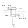
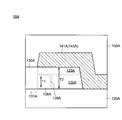
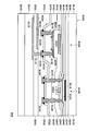
- FIG. 1 is a cross-sectional view showing an outline of a semiconductor device according to an embodiment of the present invention.
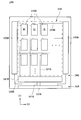
- FIG. 2 is a plan view showing an outline of the semiconductor device according to the embodiment of the present invention.
- FIG. 3 is an enlarged cross-sectional view of a part of the semiconductor device according to the embodiment of the present invention.
- the semiconductor device 10 is provided above the substrate 100.
- the semiconductor device 10 includes a first gate electrode 110, a first gate insulating layer 120, a first oxide semiconductor layer 130, a first source electrode 141, a first drain electrode 143, a first insulating layer 150, an oxide layer 160, and a first. It has one source wiring 171 and a first drain wiring 173.
- these electrodes may be referred to as the first electrode 140.
- the first source wiring 171 and the first drain wiring 173 are not particularly distinguished, these wirings may be referred to as the first conductive layer 170.
- the first gate electrode 110 is provided on the substrate 100.
- the first gate electrode 110 faces the first oxide semiconductor layer 130.
- the first gate insulating layer 120 is provided between the first gate electrode 110 and the first oxide semiconductor layer 130.
- the first electrode 140 is provided on the first gate insulating layer 120 and on the first oxide semiconductor layer 130.
- the first electrode 140 rides on the pattern end portion of the first oxide semiconductor layer 130 from the upper surface of the first gate insulating layer 120 and continues to the upper surface of the first oxide semiconductor layer 130. That is, the first electrode 140 is in contact with the first oxide semiconductor layer 130 from above the first oxide semiconductor layer 130.
- the first oxide semiconductor layer 130 is an oxide semiconductor containing indium.
- the first oxide semiconductor layer 130 includes a channel region 131 between the first source electrode 141 and the first drain electrode 143. That is, each of the first source electrode 141 and the first drain electrode 143 is in contact with the first oxide semiconductor layer 130 at the end of the channel region 131.
- Indium contained in the first oxide semiconductor layer 130 is unevenly distributed in the first oxide semiconductor layer 130 below the first source electrode 141 and the first drain electrode 143. In other words, indium contained in the first oxide semiconductor layer 130 is unevenly distributed in the first oxide semiconductor layer 130 in the region overlapping the first electrode 140 in a plan view.
- the first oxide semiconductor layer 130 below the first electrode 140 (in the region overlapping the first electrode 140 in a plan view) of the first oxide semiconductor layer 130, the first oxide semiconductor layer 130 It has been found that the reliability of the semiconductor device 10 is improved by segregating the indium contained in the first oxide semiconductor layer 130 so that the indium is unevenly distributed.
- the first insulating layer 150 covers the first oxide semiconductor layer 130 and the first electrode 140.
- the first insulating layer 150 is provided with first openings 151 and 153.
- the first opening 151 is an opening that reaches the first source electrode 141.
- the first opening 153 is an opening that reaches the first drain electrode 143.
- the oxide layer 160 is provided on the first insulating layer 150.
- the oxide layer 160 is provided with second openings 161 and 163.
- the second opening 161 is an opening continuous with the first opening 151.
- the second opening 163 is an opening continuous with the first opening 153.
- the first conductive layer 170 is provided on the oxide layer 160 and inside the first openings 151 and 153. In a plan view, the first conductive layer 170 is provided in the same region as the oxide layer 160, except for the first openings 151 and 153. That is, the oxide layer 160 is not provided in the region where the first conductive layer 170 is not provided in a plan view, and the first insulating layer 150 is exposed from the oxide layer 160.
- the first conductive layer 170 is in contact with the first electrode 140 at the bottom of the first openings 151 and 153, and is electrically connected to the first oxide semiconductor layer 130 via the first electrode 140.
- the first oxide semiconductor layer 130 is provided inside the first gate electrode 110 in a plan view.
- the first oxide semiconductor layer 130 is provided inside the first gate electrode 110.
- the outer edge of the pattern of the first oxide semiconductor layer 130 is surrounded by the outer edge of the pattern of the first gate electrode 110.
- the first electrode 140 crosses the first oxide semiconductor layer 130.
- the first electrode 140 intersects the first oxide semiconductor layer 130.
- the second opening 161 overlaps with the first opening 151 in a plan view.
- the second opening 163 overlaps with the first opening 153 in a plan view.
- Indium contained in the first oxide semiconductor layer 130 is unevenly distributed in the first oxide semiconductor layer 130 in the region overlapping the first electrode 140 in a plan view.
- the above configuration is merely one embodiment, and the present invention is not limited to the above configuration.
- FIG. 3 is an enlarged view of the area surrounded by the dotted line frame in FIG.
- the first oxide semiconductor layer 130 is provided with a channel region 131, a first region 133, and a second region 135.
- the channel region 131 is a region in which the first electrode 140 is not provided above the first oxide semiconductor layer 130.
- the first region 133 and the second region 135 are regions in which the first electrode 140 is provided above the first oxide semiconductor layer 130.
- the channel region 131 is a region in which the first oxide semiconductor layer 130 is exposed from the first electrode 140 in a plan view.
- the first region 133 and the second region 135 are regions in which the first oxide semiconductor layer 130 overlaps with the first electrode 140 in a plan view.
- the channel region 131, the first region 133, and the second region 135 are each formed of one oxide semiconductor layer, and all have the same composition and the same crystal state immediately after the film formation. However, the composition and crystal state of the first oxide semiconductor layer 130 in each of the above regions are different due to the influence of the manufacturing process of the semiconductor device 10.
- the indium contained in the first oxide semiconductor layer 130 is unevenly distributed.
- indium is not unevenly distributed in the first oxide semiconductor layer 130 in the channel region 131.
- the presence or absence of uneven distribution of indium in the first oxide semiconductor layer 130 may differ depending on the evaluation method and evaluation accuracy. If it is evaluated that indium is unevenly distributed in the first oxide semiconductor layer 130 in the channel region 131, the first region 133 and the second region 135 are the first oxide semiconductors as compared with the channel region 131.
- the degree of uneven distribution of indium in the layer 130 is large.
- the degree of uneven distribution of indium in the first oxide semiconductor layer 130 is larger in the second region 135 than in the first region 133.
- the large degree of uneven distribution of indium means that the region where indium is unevenly distributed is relatively large, and the size of the region where the concentration of indium is high (high concentration region) is relatively large compared to other regions. Alternatively, it means that the size (or crystal grain size) of crystallized indium is relatively large.
- a cross-sectional TEM (Transmission Electron Microscope) image a cross-sectional STEM (Scanning Transmission Electron Microscope) image, or a cross-sectional SEM (Scanning Electron Microscope) image, a cross-sectional SEM (Scanning Electron Microscope)
- a cross-sectional SEM Scanning Electron Microscope
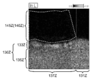
- FIG. 4 is a cross-sectional TEM image of the semiconductor device according to the embodiment of the present invention.
- the first electrode 140 a structure in which titanium (Ti) and aluminum (Al) are laminated from the bottom is used.
- the titanium layer 145 and the aluminum layer 147 have different patterns in cross-sectional view due to their different crystal states.
- an oxide semiconductor (IGZO) containing indium (In), gallium (Ga), zinc (Zn), and oxygen (O) is used.
- the region where the first electrode 140 is not provided above the channel region 131 is the channel region 131
- the region where the first electrode 140 is provided above the channel region 133 is the first region 133 and the second. Corresponds to region 135.
- heavier elements are displayed darker.
- the size of the mass of the “dark” portion of the first oxide semiconductor layer 130 in the first region 133 and the second region 135 is the size of the first in the channel region 131. It is larger than the size of the mass of the "dark” portion of the oxide semiconductor layer 130.
- the expressions "bright” and “dark” mean light and dark in the contrast of the cross-sectional image.
- the size of the mass of the "dark" portion of the first oxide semiconductor layer 130 in the second region 135 is larger than the size of the mass of the "dark” portion of the first oxide semiconductor layer 130 in the first region 133. That is, the degree of uneven distribution of indium in the first oxide semiconductor layer 130 is larger in the first region 133 and the second region 135 than in the channel region 131. The degree of uneven distribution of indium in the first oxide semiconductor layer 130 is larger in the second region 135 than in the first region 133. Since the uneven distribution of indium is considered to be caused by the crystallization of indium, it is said that the crystal grain size of indium unevenly distributed in the first oxide semiconductor layer 130 is larger in the second region 135 than in the first region 133. be able to. A mixed crystal region in which titanium and aluminum have reacted is formed between the titanium layer 145 and the aluminum layer 147.
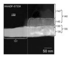
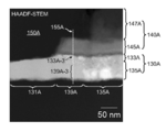
- FIG. 5A is a cross-sectional STEM image of the semiconductor device according to the embodiment of the present invention.
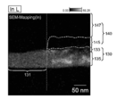
- FIG. 5B is an EDX mapping measurement result of the semiconductor device according to the embodiment of the present invention.
- the cross-section STEM image and the EDX mapping measurement sample shown in FIGS. 5A and 5B are the same as the sample of the cross-section TEM image shown in FIG.
- the STEM image shown in FIG. 5A is a HAADF (High-Angle Anal Dark Field) -STEM image. That is, in FIG. 5A, heavy elements are displayed brightly.
- the STEM image shown in FIG. 5A and the EDX mapping image shown in FIG. 5B are measurements of the same location on the same sample.
- the top and bottom are located at positions corresponding to the ends of the first electrode 140 (the lower left end of the titanium layer 145 of the first electrode 140 in FIGS. 5A and 5B).
- a dotted line extending in the direction is shown.
- the region corresponding to the titanium layer 145 is surrounded by a dotted line.
- the channel region 131 of the first oxide semiconductor layer 130 is a region in which the uniformity of indium is higher than that of other regions.
- the channel region 131 of the first oxide semiconductor layer 130 is a region in which the size of the mass of the “bright” portion is smaller than that of the other regions. That is, the channel region 131 is a region in the first oxide semiconductor layer 130 where indium is not unevenly distributed.
- the first region 133 and the second region 135 are both regions in which indium is unevenly distributed in the first oxide semiconductor layer 130. Comparing the first region 133 and the second region 135, the size of the mass of the "bright" portion in the second region 135 is larger than the size of the mass of the "bright” portion in the first region 133.
- the intensity of indium in the EDX analysis is higher in the “bright” portion confirmed in the STEM image of FIG. 5A than in the other portions. That is, indium is densely packed in the "bright” part of the STEM image.
- the region where the "bright” part lumps exist is called the "indium dense region” because the region where the indium is densely present, and the region where the "dark” part lumps exist is deficient in indium. It is called “indium deficient region” because it is in the region.
- the region where indium is unevenly distributed is a region including an indium-dense region and an indium-deficient region.
- the degree of uneven distribution of indium in the first oxide semiconductor layer 130 is larger in the second region 135 than in the first region 133. Similar to the above, since the uneven distribution of indium is considered to be caused by the crystallization of indium, the indium crystal grains unevenly distributed in the first oxide semiconductor layer 130 in the second region 135 than in the first region 133. It can be said that the diameter is large.
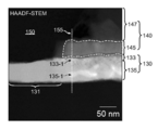
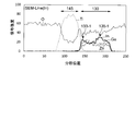
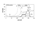
- FIGS. 6A, 6B, 7A, and 7B are EDX ray analysis results of measuring a cross-sectional STEM image of the semiconductor device according to the embodiment of the present invention and a part thereof.
- the sample of the cross-section STEM image shown in FIGS. 6A and 7A is the same as the sample of the cross-section STEM image shown in FIG. 5A.
- the region where the EDX line analysis was performed is shown by the dotted line 155.
- the horizontal axis represents the analysis position in the line analysis
- the vertical axis represents the signal intensity of each element.
- the EDX line analysis results show the spectra of indium (In), gallium (Ga), zinc (Zn), oxygen (O), and titanium (Ti).
- the range of the horizontal axis in the graph of the EDX line analysis result the range corresponding to the first oxide semiconductor layer 130 and the first electrode 140 is shown.
- indium-dense regions 133-1 and 135-1 both see FIG. 6A and 133-2 and 135-2 (both of FIGS. 7A) in the first region 133 and the second region 135, respectively. See) exists.
- a peak is confirmed in the spectrum of In in these indium-dense regions.
- the signal intensities of Ga, Zn, and O decrease in the region where the In peak exists. That is, it is considered that In is densely or crystallized in the indium dense regions 135-1 and 135-2, and a composition different from that of IGZO is locally formed.
- Method of forming an uneven distribution region of indium on the first oxide semiconductor layer 130 Various methods can be mentioned as a method for forming an uneven distribution region of indium in the first oxide semiconductor layer 130, and an example of the method will be described. For example, in a state where the first insulating layer 150 is formed on the first electrode 140, the first oxide semiconductor layer 130 below the first electrode 140 is heated to lower the first electrode 140. An uneven distribution region of indium can be formed on the first oxide semiconductor layer 130.
- a method of irradiating the first electrode 140 with a laser beam from above is used as a method of locally heating the first oxide semiconductor layer 130 below the first electrode 140.
- the wavelength of the laser light it is possible to select a wavelength having a higher absorption rate of the laser light for the first electrode 140 than for the absorption rate of the laser light for the first oxide semiconductor layer 130.
- the first electrode 140 can be selectively heated by irradiating the laser from above the first electrode 140 using the laser beam having such a wavelength. Therefore, the first oxide semiconductor layer 130 below the first electrode 140 can be selectively heated at a high temperature.
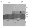
- FIG. 8 is a cross-sectional TEM image of a conventional semiconductor device.
- 9A and 9B are cross-sectional STEM images of a conventional semiconductor device and corresponding EDX mapping measurement results.
- the semiconductor device 10Z shown in FIG. 8 is the same as the semiconductor device 10 shown in FIG. 4, except that indium is not unevenly distributed in the first oxide semiconductor layer 130Z as shown below. That is, the film forming conditions of each layer constituting the semiconductor device 10Z are the same as the film forming conditions of each layer constituting the semiconductor device 10.
- FIG. 8 is a cross-sectional TEM image corresponding to FIG. Similar to FIG. 4, the structure of the first electrode 140Z shown in FIG. 8 is a structure in which a titanium layer 145Z and an aluminum layer 147Z are laminated from the bottom. Unlike FIG. 4, a mixed crystal region in which titanium and aluminum have reacted is not formed between the titanium layer 145Z and the aluminum layer 147Z. IGZO is used as the first oxide semiconductor layer 130Z.
- the region above which the first electrode 140Z is not provided is the channel region 131Z, and the region above which the first electrode 140Z is provided is the fourth region. It is 137Z.
- the fourth region 137Z is a region corresponding to the first region 133 and the second region 135 in FIG.
- the “bright” portion and the “dark” portion are substantially uniformly present. are doing.
- the sample of the cross-sectional STEM image shown in FIG. 9A is not exactly the same as the sample of the cross-sectional TEM image shown in FIG. 8, but the cross-sectional structure of each sample is the same.
- the end portion of the first electrode 140Z the lower right end portion of the titanium layer 145Z of the first electrode 140Z in each of FIGS. 9A and 9B.
- a dotted line extending vertically is shown at the corresponding position.
- the region corresponding to the titanium layer 145Z is surrounded by a dotted line.
- uneven distribution of indium is not confirmed in the first oxide semiconductor layer 130Z in the channel region 131Z and the fourth region 137Z.
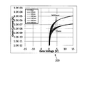
- FIG. 10A is a diagram showing the reliability test results of a conventional semiconductor device.
- FIG. 10B is a diagram showing the reliability test results of the semiconductor device according to the embodiment of the present invention.
- the test result 200 shown in FIG. 10B is the result of the reliability test performed on the semiconductor device 10 of the first embodiment
- the test result 200Z shown in FIG. 10A is the result of the reliability test performed on the conventional semiconductor device 10Z. It is the result of the sex test.
- the [channel length / channel width] of the semiconductor device used in the test is [3.5 ⁇ m / 4.0 ⁇ m].
- the reliability test of FIGS. 10A and 10B is a test for evaluating NBTIS (Negative Bias Thermal Illumination Stress) stress reliability.
- the conditions of the reliability test are as follows. -Light irradiation conditions: White LED 8,000 nits ⁇ Gate voltage: -30V ⁇ Source and drain voltage: 0V ⁇ Stage temperature when stress is applied: 60 ° C
- FIGS. 10A and 10B the results of evaluating the electrical characteristics of the respective semiconductor devices are superimposed and displayed before the stress is applied (0 sec) and after each stress application time (100 sec to 3600 sec) has elapsed.
- the measurement conditions for the electrical characteristics of the semiconductor device before and after the stress is applied are as follows. -Source-drain voltage: 0.1V, 10V -Gate scanning voltage: -15V to 15V -Measurement environment: Dark room-Stage temperature at the time of measurement: 60 ° C (or "RT (room temperature)"
- the threshold value of both the semiconductor device 10 of the first embodiment and the conventional semiconductor device 10Z is negatively shifted as the stress application time increases.
- the negative shift amount of the threshold value is about 10 V by applying stress for 3600 sec (see FIG. 10A)
- the negative shift of the threshold value is obtained even when stress is applied for the same time.
- the amount is about 2V (see FIG. 10B).
- the structural differences between the semiconductor device 10 of the first embodiment and the conventional semiconductor device 10Z are as follows.
- indium contained in the first oxide semiconductor layer 130 is unevenly distributed in the first oxide semiconductor layer 130 in the region overlapping the first electrode 140 in a plan view.
- the semiconductor device 10Z there is no uneven distribution of indium in the first oxide semiconductor layer 130Z. Therefore, by unevenly distributing indium in the first oxide semiconductor layer 130 in the region (first region 133 and second region 135) overlapping with the first electrode 140 in a plan view like the semiconductor device 10, at least the above-mentioned NBTIS It was found that the reliability in the test can be improved. If indium is unevenly distributed in the first oxide semiconductor layer 130 of the channel region 131, the characteristics of the semiconductor device 10 are adversely affected. Therefore, it is preferable to form the indium unevenly distributed region only in the first region 133 and the second region 135.
- a flexible substrate containing a resin such as a polyimide substrate, an acrylic substrate, a siloxane substrate, or a fluororesin substrate
- Impurities may be introduced into the above resin in order to improve the heat resistance of the substrate 100.
- the substrate 100 does not need to be transparent, so impurities that deteriorate the transparency of the substrate 100 can be used.
- a rigid substrate having translucency and not having flexibility such as a glass substrate, a quartz substrate, and a sapphire substrate, can be used as the substrate 100. ..
- the substrate 100 has translucency such as a semiconductor substrate such as a silicon substrate, a silicon carbide substrate, or a compound semiconductor substrate, or a conductive substrate such as a stainless steel substrate. No substrate can be used.
- a general metal material can be used as the first gate electrode 110, the first electrode 140, and the first conductive layer 170.
- these members aluminum (Al), titanium (Ti), chromium (Cr), cobalt (Co), nickel (Ni), molybdenum (Mo), hafnium (Hf), tantalum (Ta), tungsten (W). ), Bismuth (Bi), silver (Ag), and alloys or compounds thereof.
- the first gate electrode 110, the first electrode 140, and the first conductive layer 170 the above materials may be used in a single layer or in a laminated manner.
- a metal material that becomes a more stable metal oxide than the oxide of the metal constituting the first oxide semiconductor layer 130 can be used. .. That is, when there are a plurality of metal elements constituting the first oxide semiconductor layer 130, the oxidation of the metal in contact with the first oxide semiconductor layer 130 is based on the Gibbs free energy ( ⁇ G f ) of each metal oxide of the plurality of metal elements. It is preferable that the Gibbs free energy of the metal is smaller.
- IGZO when IGZO is used as the first oxide semiconductor layer 130, Ti can be used as the metal in contact with IGZO.
- the Gibbs free energy of In oxide is larger than the Gibbs free energy of Ga oxide and Zn oxide. That is, In oxide is scientifically more unstable and more likely to be reduced.
- the Gibbs free energy of Ti oxide is sufficiently smaller than that of Ga oxide and Zn oxide, when Ti is formed on IGZO, Ti combines with oxygen in IGZO to form Ti oxide. Since In oxide is easily reduced as described above, when high energy is supplied in a state where IGZO and Ti are in contact with each other, In oxide is reduced and Ti is oxidized. As a result, even in the step after the first electrode 140 is formed on the first oxide semiconductor layer 130, an uneven distribution region of indium can be generated in the first oxide semiconductor layer 130.
- a general insulating layer material can be used as the first gate insulating layer 120 and the first insulating layer 150.
- an insulating layer having few defects can be used.
- composition ratio of oxygen in the first insulating layer 150 and the composition ratio of oxygen in the insulating layer having the same composition as the first insulating layer 150 are compared, the other The composition ratio of oxygen in the first insulating layer 150 is closer to the chemical quantity theory ratio to the insulating layer having the same composition as that of the first insulating layer 150 than the composition ratio of oxygen in the insulating layer.
- SiO x N y and AlO x N y described above are silicon compounds and aluminum compounds containing nitrogen (N) in a ratio (x> y) smaller than that of oxygen (O).
- SiN x Oy and AlN x Oy are silicon compounds and aluminum compounds containing oxygen in a ratio (x> y) smaller than that of nitrogen.
- a metal oxide having semiconductor characteristics can be used.
- an oxide semiconductor containing indium (In), gallium (Ga), zinc (Zn), and oxygen (O) can be used.
- the oxide semiconductor containing In, Ga, Zn, and O used in the present embodiment is not limited to the above composition, and an oxide semiconductor having a composition different from the above can also be used.
- the ratio of In may be larger than the above in order to improve the mobility.
- the ratio of Ga may be larger than the above in order to increase the band gap and reduce the influence of light irradiation.
- oxide semiconductor containing In, Ga, Zn, and O may be added to the oxide semiconductor containing In, Ga, Zn, and O, and for example, metal elements such as Al and Sn may be added.
- oxide semiconductors containing In and Ga IGO
- oxide semiconductors containing In and Zn IZO
- oxide semiconductors containing In, Sn and Zn IGO
- An oxide semiconductor containing the above can be used as the first oxide semiconductor layer 130.
- the first oxide semiconductor layer 130 may be amorphous or crystalline.
- the first oxide semiconductor layer 130 may be a mixed phase of amorphous and crystalline.
- a physical insulation layer can be used.
- the oxide layer 160 is preferably formed by a sputtering method.
- the process gas used in the sputtering remains in the film of the oxide layer 160.
- Ar is used as the sputtering process gas
- Ar remains in the film of the oxide layer 160.
- the remaining Ar can be detected by SIMS (Secondary Ion Mass Spectrometry) analysis on the oxide layer 160.
- SIMS Secondary Ion Mass Spectrometry
- indium is not unevenly distributed in the first oxide semiconductor layer 130 of the channel region 131, and the first oxide semiconductor of the first region 133 and the second region 135 is not unevenly distributed.
- the reliability of the semiconductor device 10 can be improved.
- the bottom gate type semiconductor device 10 in which the first gate electrode 110 is provided below the first oxide semiconductor layer 130 is shown, but in the semiconductor device, the gate electrode is an oxide semiconductor layer. It may be a top gate type semiconductor device provided above.
- the oxide layer 160 is provided between the first insulating layer 150 and the first conductive layer 170 is exemplified, but the configuration is not limited to this configuration.
- the oxide layer 160 may be omitted, and the first conductive layer 170 may be in contact with the upper surface of the first insulating layer 150.
- the oxide layer 160 may be provided on the side wall of the first openings 151 and 153.
- the oxide layer 160 may be provided in the region where the first conductive layer 170 is not provided.
- the oxide layer 160 may be provided above the first oxide semiconductor layer 130. In other words, in plan view, the oxide layer 160 may overlap with the first oxide semiconductor layer 130.
- each layer is composed of one layer, but each layer may have a laminated structure.
- FIG. 11 is a cross-sectional view showing an outline of the semiconductor device according to the embodiment of the present invention.
- the cross-sectional view shown in FIG. 11 corresponds to the cross-sectional view shown in FIG.
- the semiconductor device 10A shown in FIG. 11 is similar to the semiconductor device 10 shown in FIGS. 1 to 3, except that the region where indium is unevenly distributed in the first oxide semiconductor layer 130A below the first electrode 140A is different. , Different from the semiconductor device 10.
- the same features as the semiconductor device 10 will be omitted, and the differences from the semiconductor device 10 will be mainly described.
- the first oxide semiconductor layer 130A includes a channel region 131A, a first region 133A, a second region 135A, and a third region 139A.
- the channel region 131A is a region in which the first electrode 140A is not provided above the first oxide semiconductor layer 130A.
- the first region 133A, the second region 135A, and the third region 139A are regions in which the first electrode 140A is provided above the first oxide semiconductor layer 130A.
- the channel region 131A is a region exposed from the first electrode 140A in a plan view.
- the first region 133A, the second region 135A, and the third region 139A are regions that overlap with the first electrode 140A in a plan view.
- the third region 139A is provided between the first gate insulating layer 120A and the first region 133A.
- the third region 139A is provided between the channel region 131A and the second region 135A.
- the third region 139A extends from below the end of the first electrode 140A on the channel region 131A side toward the inside of the pattern of the first electrode 140A.
- the third region 139A includes a square 138A having a predetermined size in a cross-sectional view.
- the square 138A in cross-sectional view, is surrounded by the outer edge of the third region 139A.
- the square 138A in cross-sectional view is a square in which the length of one side is at least half the length of the film thickness of the first oxide semiconductor layer 130A in the region overlapping with the first electrode 140A in plan view.
- the length T1 of one side of the square 138A included in the third region 139A is half the film thickness T2 of the first oxide semiconductor layer 130A in the region overlapping the first electrode 140A in a plan view (T2 / 2). ) It is longer than that.
- the vertical and horizontal widths of the third region 139A in a cross-sectional view are larger than half (T2 / 2) of the film thickness T2 of the first oxide semiconductor layer 130A.
- the semiconductor device 10A according to the second embodiment has the effect of improving the electrical characteristics of the semiconductor device 10A by providing the third region 139A having the following characteristics. This effect is remarkable when the third region 139A satisfies the above conditions.
- the channel region 131A, the first region 133A, the second region 135A, and the third region 139A are each formed from one oxide semiconductor layer, and all have the same composition and the same crystal state immediately after film formation. Is. However, in the first oxide semiconductor layer 130A, the composition and the crystal state of the first oxide semiconductor layer 130A in each of the above regions are different due to the influence of the manufacturing process of the semiconductor device 10A.
- the degree of uneven distribution of indium in the channel region 131A, the first region 133A, and the second region 135A is the same as that in the first embodiment, the description thereof will be omitted.
- indium is not unevenly distributed as in the channel region 131A.
- the presence or absence of indium uneven distribution in the first oxide semiconductor layer 130A may differ depending on the evaluation method and evaluation accuracy, but it is assumed that indium is unevenly distributed in the first oxide semiconductor layer 130A in the third region 139A. When this is done, the degree of uneven distribution of indium in the first oxide semiconductor layer 130A is smaller in the third region 139A than in the first region 133A and the second region 135A.
- indium is more uniformly present than in the first region 133A and the second region 135A.
- the degree of uneven distribution of indium in the channel region 131A and the third region 139A is almost the same. That is, for example, in the observation result of the cross-section TEM image, the cross-section STEM image, the cross-section SEM image, or the surface analysis of the EDX, there is almost no difference between the channel region 131A and the third region 139A.
- the first oxide semiconductor layer 130A of each of the channel region 131A and the third region 139A is continuously connected.
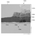
- FIG. 12 is a cross-sectional TEM image of the semiconductor device according to the embodiment of the present invention. Similar to FIG. 4, a structure in which a titanium layer 145A and an aluminum layer 147A are laminated from below is used as the first electrode 140A. IGZO is used as the first oxide semiconductor layer 130A.
- FIG. 12 the positions of the channel region 131A, the first region 133A, the second region 135A, and the third region 139A are as shown in the drawings.
- a first region 133A is provided below the first electrode 140A, and a second region 135A and a third region 139A are provided adjacent to each other below the first region 133A.
- the third region 139A is provided between the channel region 131A and the second region 135A.
- the first oxide semiconductor layer 130A in the third region 139A has a “bright” portion in terms of contrast in the cross-sectional image, similarly to the first oxide semiconductor layer 130A in the channel region 131A.
- the "dark” part is present almost uniformly. Therefore, it is determined that indium is not unevenly distributed in the first oxide semiconductor layer 130A in the third region 139A.
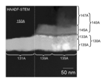
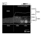
- FIG. 13A and 13B are a cross-sectional STEM image of the semiconductor device according to the embodiment of the present invention and the corresponding EDX mapping measurement results.
- the sample of the cross-section STEM image shown in FIG. 13A is the same as the sample of the cross-section TEM image shown in FIG.
- the upper and lower ends correspond to the ends of the first electrode 140A (the lower left end of the titanium layer 145A of the first electrode 140A in FIGS. 13A and 13B).
- a dotted line extending in the direction is shown.
- the region corresponding to the titanium layer 145A is surrounded by a dotted line.
- the channel region 131A and the third region 139A of the first oxide semiconductor layer 130A are regions having higher uniformity than the other regions.
- the channel region 131A and the third region 139A of the first oxide semiconductor layer 130A are regions in which the size of the mass of the “bright” portion is smaller than that of the other regions. That is, the channel region 131A and the third region 139A are regions in which the indium is not unevenly distributed in the first oxide semiconductor layer 130A.
- the first oxide semiconductor layer 130A in the channel region 131A and the third region 139A is indium as compared with the first oxide semiconductor layer 130A in the first region 133A and the second region 135A.
- Indium is unevenly distributed in the first oxide semiconductor layer 130A of the first region 133A and the second region 135A.
- FIGS. 14A, 14B, 15A, and 15B are EDX line analysis results obtained by measuring a cross-sectional STEM image of a semiconductor device according to an embodiment of the present invention and a part thereof.
- the sample of the cross-section STEM image shown in FIGS. 14A and 15A is the same as the sample of the cross-section STEM image shown in FIG. 13A.
- the region where the EDX line analysis was performed is shown by the dotted line. Since each spectrum shown in the EDX line analysis results of FIGS. 14B and 15B is the same as that of FIG. 6, the description thereof will be omitted.
- indium dense regions 133A-3 (see FIG. 14A) and 135A-4 (see FIG. 15A) are present in the first region 133A and the second region 135A, respectively.
- a peak is confirmed in the spectrum of In in these indium-dense regions.
- the signal intensities of Ga, Zn, and O decrease in the region where a large peak of In exists. That is, it is considered that In is densely or crystallized in the indium dense region 135A-4, and a composition different from that of IGZO is locally formed.
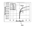
- FIG. 16A is a diagram showing the electrical characteristics of the semiconductor device according to the first embodiment of the present invention.
- FIG. 16B is a diagram showing the electrical characteristics of the semiconductor device according to the second embodiment of the present invention.
- the electrical characteristic 210 of FIG. 16A is the electrical characteristic of the semiconductor device 10 of the first embodiment.
- the electrical characteristic 210A of FIG. 16B is the electrical characteristic of the semiconductor device 10A of the second embodiment.
- the [channel length / channel width] of the semiconductor device used in the test is [3.5 ⁇ m / 4.0 ⁇ m].
- the measurement conditions for the electrical characteristics shown in FIGS. 16A and 16B are as follows. -Source-drain voltage: 0.1V, 10V -Gate scanning voltage: -15V to 15V ⁇ Measurement environment: Dark room ⁇ Stage temperature at the time of measurement: R. T.
- the semiconductor device 10A (electrical characteristic 210A) according to the second embodiment has a steeper ON current rise than the semiconductor device 10 (electrical characteristic 210) according to the first embodiment. is there.
- the structural difference between the semiconductor device 10 according to the first embodiment and the semiconductor device 10A according to the second embodiment is that in the semiconductor device 10, the second region 135 in which indium is unevenly distributed exists up to the vicinity of the channel region 131.
- indium is not segregated between the channel region 131A and the second region 135A (or the degree of uneven distribution of indium is smaller than that of the second region 135A). This is the point where the region 139A exists.
- the above-mentioned third region 139A needs to have a certain size or more. As shown in FIG. 16, in order to obtain the electrical characteristic in which the ON current rises sharply, the third region 139A needs to be continuously present in a region wider than the square 138A (see FIG. 11).
- the length T1 of one side of the square 138A is at least half (T2 / 2) of the film thickness T2 of the first oxide semiconductor layer 130A in the region overlapping with the first electrode 140A in a plan view.
- the configuration is illustrated, but is not limited to this configuration.
- the length T1 of one side of the square 138A may be 60% or more, 70% or more, 80% or more, or 90% or more of the film thickness T2.
- indium contained in the first oxide semiconductor layer 130 is unevenly distributed (or crystallized) in the first oxide semiconductor layer 130 below the first electrode 140, so that at least NBTIS is used.
- the reliability in the test can be improved.
- the second region 135 exists up to the vicinity of the channel region 131 as shown in the first embodiment, the rise of the ON current becomes gentle.
- IZGO it is known that a conduction band is formed by the 5s orbit of indium. If the composition of IZGO is biased due to the uneven distribution of indium as in the second region 135, it is considered that the conduction path is interrupted and the resistance as the IZGO film increases. For this reason, in the case of the semiconductor device 10 of the first embodiment, the resistance value of the first oxide semiconductor layer 130 in the second region 135 near the channel region 131 is high, so that the rise of the ON current becomes slow. Guess.
- the third region 139A between the channel region 131A and the second region 135A is a region in which indium is not unevenly distributed
- the first oxide semiconductor in the third region 139A The resistance value of the layer 130A is considered to be smaller than the resistance value of the first oxide semiconductor layer 130A in the second region 135A.
- the reliability of the semiconductor device 10A in the NBTIS test is also improved as compared with the conventional semiconductor device 10Z (see FIG. 10A) as well as the reliability of the semiconductor device 10 (see FIG. 10B).
- the test result 200A is the result of the reliability test performed on the semiconductor device 10A of the second embodiment.
- the reliability can be improved as in the semiconductor device 10 according to the first embodiment, and the rise of the ON current is steep as described above. Electrical characteristics can be obtained.
- FIGS. 18 to 22 A display device using a semiconductor device according to an embodiment of the present invention will be described with reference to FIGS. 18 to 22.
- a configuration in which the semiconductor device described in the first and second embodiments described above is applied to a circuit of a liquid crystal display device will be described.
- FIG. 18 is a plan view showing an outline of a display device according to an embodiment of the present invention.
- the display device 20B includes an array substrate 300B, a seal portion 400B, a facing substrate 500B, a flexible printed circuit board 600B (FPC600B), and an IC chip 700B.
- the array substrate 300B and the facing substrate 500B are bonded by the seal portion 400B.
- a plurality of pixel circuits 310B are arranged in a matrix in the liquid crystal region 22B surrounded by the seal portion 400B.
- the liquid crystal region 22B is a region that overlaps with the liquid crystal element 410B described later in a plan view.
- the seal area 24B provided with the seal portion 400B is an area around the liquid crystal area 22B.
- the FPC 600B is provided in the terminal area 26B.
- the terminal region 26B is a region where the array substrate 300B is exposed from the facing substrate 500B, and is provided outside the seal region 24B.
- the outside of the seal region 24B means the outside of the region where the seal portion 400B is provided and the region surrounded by the seal portion 400B.
- the IC chip 700B is provided on the FPC 600B.
- the IC chip 700B supplies a signal for driving each pixel circuit 310B.
- FIG. 19 is a block diagram showing a circuit configuration of a display device according to an embodiment of the present invention.
- a source driver circuit 320B is provided at a position adjacent to the liquid crystal region 22B in which the pixel circuit 310B is arranged in the D1 direction (column direction), and is provided in the D2 direction with respect to the liquid crystal region 22B.
- a gate driver circuit 330B is provided at a position adjacent to (row direction).
- the source driver circuit 320B and the gate driver circuit 330B are provided in the above-mentioned seal region 24B.
- the region where the source driver circuit 320B and the gate driver circuit 330B are provided is not limited to the seal region 24B, and may be any region as long as it is outside the region where the pixel circuit 310B is provided.
- the source wiring 321B extends from the source driver circuit 320B in the D1 direction, and is connected to a plurality of pixel circuits 310B arranged in the D1 direction.
- Gate wiring 331B extends in the D2 direction from the gate driver circuit 330B and is connected to a plurality of pixel circuits 310B arranged in the D2 direction.
- a terminal portion 333B is provided in the terminal area 26B.
- the terminal portion 333B and the source driver circuit 320B are connected by the connection wiring 341B.
- the terminal portion 333B and the gate driver circuit 330B are connected by the connection wiring 341B.
- the semiconductor device shown in the first embodiment and the second embodiment is applied to the transistors included in the pixel circuit 310B, the source driver circuit 320B, and the gate driver circuit 330B.
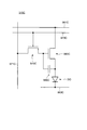
- FIG. 20 is a circuit diagram showing a pixel circuit of a display device according to an embodiment of the present invention.
- the pixel circuit 310B includes elements such as a transistor 800B, a holding capacity 890B, and a liquid crystal element 410B.
- the transistor 800B has a first gate electrode 810B, a first source electrode 830B, and a first drain electrode 840B.
- the first gate electrode 810B is connected to the gate wiring 331B.
- the first source electrode 830B is connected to the source wiring 321B.
- the first drain electrode 840B is connected to the holding capacity 890B and the liquid crystal element 410B.
- the semiconductor device shown in the first embodiment and the second embodiment is applied to the transistor shown in FIG.
- 830B is referred to as a source electrode and 840B is referred to as a drain electrode, but the function as a source and the function as a drain of each electrode may be interchanged.
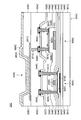
- FIG. 21 is a cross-sectional view of a display device according to an embodiment of the present invention.
- the display device 20B is a display device in which transistors 800B and 900B having different structures are provided on the same substrate.
- the structure of the transistor 800B is different from the structure of the transistor 900B.
- the transistor 800B is a bottom gate type transistor in which the first oxide semiconductor layer 820B is used as a channel.
- the transistor 900B is a top gate type transistor in which a semiconductor layer 920B is used as a channel.
- the transistor 800B is used in the pixel circuit 310B
- the transistor 900B is used in the source driver circuit 320B and the gate driver circuit 330B.
- the transistor 900B may be used in the pixel circuit 310B.
- the transistor 800B is a transistor formed on the substrate 301B, and has insulating layers 340B, 342B, 344B, and 346B as a base layer.
- the first gate electrode 810B is provided on the insulating layer 346B.
- a first oxide semiconductor layer 820B is provided above the first gate electrode 810B.
- the first gate electrode 810B faces the first oxide semiconductor layer 820B.
- An insulating layer 348B that functions as a gate insulating layer is provided between the first gate electrode 810B and the first oxide semiconductor layer 820B.
- a first source electrode 830B is provided at one end of the pattern of the first oxide semiconductor layer 820B, and a first drain electrode 840B is provided at the other end.
- the first source electrode 830B and the first drain electrode 840B are connected to the first oxide semiconductor layer 820B on the upper surface and the side surface of the first oxide semiconductor layer 820B, respectively.
- the first insulating layers 350B and 352B are provided on the first oxide semiconductor layer 820B, the first source electrode 830B, and the first drain electrode 840B.
- the first insulating layers 350B and 352B are provided with openings 851B and 861B.
- a first source wiring 850B is provided above the first insulating layer 352B and inside the opening 851B.
- a first drain wiring 860B is provided above the first insulating layer 352B and inside the opening 861B.
- An oxide layer 853B is provided between the upper surface of the first insulating layer 352B and the first source wiring 850B.
- An oxide layer 855B is provided between the upper surface of the first insulating layer 352B and the first drain wiring 860B.
- a second insulating layer 354B is provided on the first source wiring 850B and the first drain wiring 860B.
- a common electrode 880B commonly provided for a plurality of pixels is provided on the second insulating layer 354B.
- a second insulating layer 356B is provided on the common electrode 880B.
- the second insulating layer 354B and 356B are provided with a third opening 871B.
- a pixel electrode 870B is provided on the second insulating layer 356B and inside the third opening 871B. The pixel electrode 870B is connected to the first drain wiring 860B.
- FIG. 22 is a plan view of a pixel electrode and a common electrode of the display device according to the embodiment of the present invention.
- the common electrode 880B has a superposed region that overlaps with the pixel electrode 870B in a plan view and a non-superimposed region that does not overlap with the pixel electrode 870B.
- a voltage is supplied between the pixel electrode 870B and the common electrode 880B, a transverse electric field is formed from the pixel electrode 870B in the superposed region toward the common electrode 880B in the non-superimposed region.
- the gradation of pixels is determined by the operation of the liquid crystal molecules contained in the liquid crystal element 410B by this lateral electric field.
- the semiconductor device 10 or 10A of FIGS. 1, 3 or 11 can be applied as the transistor 800B.
- each member in each drawing corresponds as follows.
- the first gate electrode 110 corresponds to the first gate electrode 810B.
- the first gate insulating layer 120 corresponds to the insulating layer 348B.
- the first oxide semiconductor layer 130 corresponds to the first oxide semiconductor layer 820B.
- the first source electrode 141 corresponds to the first source electrode 830B.
- the first drain electrode 143 corresponds to the first drain electrode 840B.
- the first insulating layer 150 corresponds to the first insulating layers 350B and 352B.
- the first opening 151 corresponds to the opening 851B.
- the first opening 153 corresponds to the opening 861B.
- the oxide layer 160 corresponds to the oxide layers 853B and 855B.
- the first source wiring 171 corresponds to the first source wiring 850B.
- the first drain wiring 173 corresponds to the first drain wiring 860B.
- the transistor 900B is a transistor formed on the substrate 301B and has an insulating layer 340B as a base layer.
- a light-shielding layer 910B is provided on the insulating layer 340B.
- An insulating layer 342B is provided on the light shielding layer 910B.
- a semiconductor layer 920B is provided on the insulating layer 342B.
- a second gate electrode 930B is provided above the semiconductor layer 920B.
- An insulating layer 344B that functions as a gate insulating layer is provided between the semiconductor layer 920B and the second gate electrode 930B. Insulating layers 346B, 348B, 350B, and 352B are provided on the second gate electrode 930B.
- These insulating layers are provided with openings 941B and 951B.
- a second source wiring 940B is provided above the insulating layer 352B and inside the opening 941B.
- a second drain wiring 950B is provided above the insulating layer 352B and inside the opening 951B.
- An insulating layer 354B is provided on the second source wiring 940B and the second drain wiring 950B.
- the second gate electrode 930B is provided below the same layer (insulation layer 348B) as the gate insulating layer of the transistor 800B.
- FIGS. 23 and 24 A display device using a semiconductor device according to an embodiment of the present invention will be described with reference to FIGS. 23 and 24.
- the configuration in which the semiconductor device described in the first and second embodiments described above is applied to the circuit of the organic EL display device will be described. Since the outline and circuit configuration of the display device 20C are the same as those shown in FIGS. 18 and 19, the description thereof will be omitted.
- FIG. 23 is a circuit diagram showing a pixel circuit of a display device according to an embodiment of the present invention.
- the pixel circuit 310C includes elements such as a drive transistor 960C, a selection transistor 970C, a holding capacity 980C, and a light emitting element DO.
- the source electrode of the selection transistor 970C is connected to the signal line 971C, and the gate electrode of the selection transistor 970C is connected to the gate line 973C.
- the source electrode of the drive transistor 960C is connected to the anode power supply line 961C, and the drain electrode of the drive transistor 960C is connected to one end of the light emitting element DO.
- the other end of the light emitting element DO is connected to the cathode power line 963C.
- the gate electrode of the drive transistor 960C is connected to the drain electrode of the selection transistor 970C.
- the holding capacity 980C is connected to the gate electrode and the drain electrode of the drive transistor 960C.
- a gradation signal that determines the emission intensity of the light emitting element DO is supplied to the signal line 971C.
- a signal for selecting a pixel row for writing the gradation signal is supplied to the gate line 973C.
- FIG. 24 is a cross-sectional view of a display device according to an embodiment of the present invention.
- the configuration of the display device 20C shown in FIG. 24 is similar to that of the display device 20B shown in FIG. 21, but the structure above the insulating layer 354C of the display device 20C is the structure above the insulating layer 354B of the display device 20B. Is different from.
- the same configuration as that of the display device 20B shown in FIG. 21 will be omitted, and the differences from the display device 20B will be described.
- the display device 20C has a pixel electrode 981C, a light emitting layer 983C, and a common electrode 985C above the insulating layer 354C.
- the pixel electrode 981C is provided on the insulating layer 354C and inside the third opening 871C.
- An insulating layer 358C is provided on the pixel electrode 981C.
- the insulating layer 358C is provided with an opening 359C.
- the opening 359C corresponds to the light emitting region. That is, the insulating layer 358C defines the pixels.
- a light emitting layer 983C and a common electrode 985C are provided on the pixel electrode 981C exposed by the opening 359C.
- the pixel electrode 981C and the light emitting layer 983C are individually provided for each pixel.
- the common electrode 985C is provided in common to a plurality of pixels.
- the light emitting layer 983C different materials are used depending on the display color of the pixels.
- the semiconductor devices described in the first and second embodiments are applied to a liquid crystal display device and an organic EL display device are exemplified, but other than these display devices.
- the semiconductor device may be applied to a display device (for example, a self-luminous display device other than an organic EL display device or an electronic paper type display device).
- the above semiconductor devices can be applied to small and medium-sized display devices to large-sized display devices without particular limitation.
- the present invention also includes a device in which a person skilled in the art appropriately adds, deletes, or changes the design of a component based on the semiconductor device and the display device of each embodiment, or adds, omits, or changes the conditions of a process. As long as it has the gist of the above, it is included in the scope of the present invention.
- 10 Semiconductor device, 20B: Display device, 22B: Liquid crystal area, 24B: Seal area, 26B: Terminal area, 100: Substrate, 110: 1st gate electrode, 120: 1st gate insulating layer, 130: 1st oxide Semiconductor layer, 131: channel region, 133: first region, 133-1, 133A-3, 135-1, 135-2, 135A-4: indium dense region, 135: second region, 137Z: fourth region, 138A: Square, 139A: 3rd region, 140: 1st electrode, 141: 1st source electrode, 143: 1st drain electrode, 145: Titanium layer, 147: Aluminum layer, 150: 1st insulating layer, 151, 153 : 1st opening, 160: Oxide layer, 161, 163: 2nd opening, 170: 1st conductive layer, 171: 1st source wiring, 173: 1st drain wiring, 200: Test result, 210: Electrical characteristics, 300B
Landscapes
- Chemical & Material Sciences (AREA)
- Analytical Chemistry (AREA)
- Crystallography & Structural Chemistry (AREA)
- Physics & Mathematics (AREA)
- Health & Medical Sciences (AREA)
- Life Sciences & Earth Sciences (AREA)
- Dispersion Chemistry (AREA)
- Biochemistry (AREA)
- General Health & Medical Sciences (AREA)
- General Physics & Mathematics (AREA)
- Immunology (AREA)
- Pathology (AREA)
- Thin Film Transistor (AREA)
- Metal-Oxide And Bipolar Metal-Oxide Semiconductor Integrated Circuits (AREA)
Abstract
半導体装置は、インジウムを含む酸化物半導体層と、前記酸化物半導体層に対向するゲート電極と、前記酸化物半導体層と前記ゲート電極との間のゲート絶縁層と、前記酸化物半導体層の上方から前記酸化物半導体層に接する第1電極と、を有する。平面視で、前記第1電極と重なる領域の前記酸化物半導体層において、インジウムが偏在している。前記ゲート電極及び前記ゲート絶縁層は、前記酸化物半導体層の下方に設けられていてもよい。
Description
本発明の実施形態の一つは、半導体装置及び表示装置に関する。特に、本発明の実施形態の一つは、チャネルとして酸化物半導体が用いられた半導体装置及び当該半導体装置を用いた表示装置に関する。
最近、アモルファスシリコン、低温ポリシリコン、および単結晶シリコンに替わり、酸化物半導体をチャネルに用いた半導体装置の開発が進められている(例えば、特許文献1)。酸化物半導体をチャネルに用いた半導体装置は、アモルファスシリコンをチャネルに用いた半導体装置と同様に単純な構造かつ低温プロセスで半導体装置を形成することができる。酸化物半導体をチャネルに用いた半導体装置は、アモルファスシリコンをチャネルに用いた半導体装置よりも高い移動度を有することが知られている。酸化物半導体をチャネルに用いた半導体装置は、オフ電流が非常に低いことが知られている。
酸化物半導体をチャネルに用いた半導体装置が安定した動作をするために、その製造工程において酸化物半導体により多くの酸素を供給し、酸化物半導体に形成される酸素欠損を少なくすることが重要である。酸化物半導体に酸素を供給する方法の一つとして、特許文献1では、酸化物半導体を覆う絶縁層を、当該絶縁層が酸素をより多く含む条件で形成する技術が開示されている。
しかしながら、酸素をより多く含む条件で形成された絶縁層は欠陥を多く含む。その影響で、その欠陥に電子がトラップされることが原因と考えられる半導体装置の特性異常又は信頼性試験における特性変動が発生する。一方、欠陥の少ない絶縁層を用いると、絶縁層に含まれる酸素を多くすることができない。したがって、絶縁層から酸化物半導体に十分に酸素を供給することができない。このように、酸化物半導体を覆う絶縁層として酸素を多く含む絶縁層が用いられた場合であっても、半導体装置の信頼性を向上させるための半導体装置構造及びその製造方法を実現することが要求されている。
本発明の実施形態の一つは、信頼性が高い半導体装置を実現することを課題の一つとする。
本発明の一実施形態に係る半導体装置は、インジウムを含む酸化物半導体層と、前記酸化物半導体層に対向するゲート電極と、前記酸化物半導体層と前記ゲート電極との間のゲート絶縁層と、前記酸化物半導体層の上方から前記酸化物半導体層に接する第1電極と、を有する。平面視で前記第1電極と重なる領域の前記酸化物半導体層において、インジウムが偏在している。
以下に、本発明の各実施の形態について、図面を参照しつつ説明する。以下の開示はあくまで一例にすぎない。当業者が、発明の主旨を保ちつつ、実施形態の構成を適宜変更することによって容易に想到し得る構成は、当然に本発明の範囲に含有される。図面は説明をより明確にするため、実際の態様に比べ、各部の幅、厚さ、形状等について模式的に表される場合がある。しかし、図示された形状はあくまで一例であって、本発明の解釈を限定しない。本明細書と各図において、既出の図に関して前述したものと同様の要素には、同一の符号の後にアルファベットを付して、詳細な説明を適宜省略することがある。
本発明の各実施の形態において、基板から酸化物半導体層に向かう方向を上又は上方という。逆に、酸化物半導体層から基板に向かう方向を下又は下方という。このように、説明の便宜上、上方又は下方という語句を用いて説明するが、例えば、基板と酸化物半導体層との上下関係が図示と逆になるように配置されてもよい。以下の説明で、例えば基板上の酸化物半導体層という表現は、上記のように基板と酸化物半導体層との上下関係を説明しているに過ぎず、基板と酸化物半導体層との間に他の部材が配置されていてもよい。上方又は下方は、複数の層が積層された構造における積層順を意味し、トランジスタの上方の画素電極と表現する場合、平面視でトランジスタと画素電極とが重ならない位置関係であってもよい。一方、トランジスタの鉛直上方の画素電極と表現する場合は、平面視でトランジスタと画素電極とが重なる位置関係を意味する。
「表示装置」とは、電気光学層を用いて映像を表示する構造体を指す。例えば、表示装置という用語は、電気光学層を含む表示パネルを指す場合もあり、又は表示セルに対して他の光学部材(例えば、偏光部材、バックライト、タッチパネル等)を装着した構造体を指す場合もある。「電気光学層」には、技術的な矛盾が生じない限り、液晶層、エレクトロルミネセンス(EL)層、エレクトロクロミック(EC)層、電気泳動層が含まれ得る。したがって、後述する実施形態について、表示装置として、液晶層を含む液晶表示装置、及び有機EL層を含む有機EL表示装置を例示して説明するが、本実施形態における構造は、上述した他の電気光学層を含む表示装置へ適用することができる。
本明細書において「αはA、B又はCを含む」、「αはA,B及びCのいずれかを含む」、「αはA,B及びCからなる群から選択される一つを含む」、といった表現は、特に明示が無い限り、αがA~Cの複数の組み合わせを含む場合を排除しない。さらに、これらの表現は、αが他の要素を含む場合も排除しない。
以下の各実施形態は、技術的な矛盾を生じない限り、互いに組み合わせることができる。
〈第1実施形態〉
図1~図7を用いて、本発明の一実施形態に係る半導体装置について説明する。以下に示す実施形態の半導体装置は、表示装置に用いられるトランジスタの他に、例えば、マイクロプロセッサ(Micro-Processing Unit:MPU)などの集積回路(Integrated Circuit:IC)、又はメモリ回路に用いられてもよい。
図1~図7を用いて、本発明の一実施形態に係る半導体装置について説明する。以下に示す実施形態の半導体装置は、表示装置に用いられるトランジスタの他に、例えば、マイクロプロセッサ(Micro-Processing Unit:MPU)などの集積回路(Integrated Circuit:IC)、又はメモリ回路に用いられてもよい。
[半導体装置10の構成]
図1~図3を用いて、本発明の一実施形態に係る半導体装置10の構成について説明する。図1は、本発明の一実施形態に係る半導体装置の概要を示す断面図である。図2は、本発明の一実施形態に係る半導体装置の概要を示す平面図である。図3は、本発明の一実施形態に係る半導体装置の一部を拡大した断面図である。
図1~図3を用いて、本発明の一実施形態に係る半導体装置10の構成について説明する。図1は、本発明の一実施形態に係る半導体装置の概要を示す断面図である。図2は、本発明の一実施形態に係る半導体装置の概要を示す平面図である。図3は、本発明の一実施形態に係る半導体装置の一部を拡大した断面図である。
図1に示すように、半導体装置10は基板100の上方に設けられている。半導体装置10は、第1ゲート電極110、第1ゲート絶縁層120、第1酸化物半導体層130、第1ソース電極141、第1ドレイン電極143、第1絶縁層150、酸化物層160、第1ソース配線171、及び第1ドレイン配線173を有する。第1ソース電極141及び第1ドレイン電極143を特に区別しない場合、これらの電極を第1電極140という場合がある。第1ソース配線171及び第1ドレイン配線173を特に区別しない場合、これらの配線を第1導電層170という場合がある。
第1ゲート電極110は基板100の上に設けられている。第1ゲート電極110は第1酸化物半導体層130に対向する。第1ゲート絶縁層120は、第1ゲート電極110と第1酸化物半導体層130との間に設けられている。第1電極140は第1ゲート絶縁層120の上及び第1酸化物半導体層130の上に設けられている。第1電極140は、第1ゲート絶縁層120の上面から第1酸化物半導体層130のパターン端部に乗り上げて、第1酸化物半導体層130の上面まで連続している。つまり、第1電極140は第1酸化物半導体層130の上方から第1酸化物半導体層130に接している。
詳細は後述するが、第1酸化物半導体層130はインジウムを含む酸化物半導体である。第1酸化物半導体層130は、第1ソース電極141と第1ドレイン電極143との間にチャネル領域131を備えている。つまり、第1ソース電極141及び第1ドレイン電極143の各々は、チャネル領域131の端部において、第1酸化物半導体層130に接している。第1ソース電極141及び第1ドレイン電極143の下方における第1酸化物半導体層130中では、第1酸化物半導体層130に含まれるインジウムが偏在している。換言すると、平面視で第1電極140と重なる領域の第1酸化物半導体層130中では、第1酸化物半導体層130に含まれるインジウムが偏在している。
発明者らによって、第1酸化物半導体層130のうち第1電極140の下方の(平面視で第1電極140と重なる領域の)第1酸化物半導体層130について、第1酸化物半導体層130に含まれるインジウムを偏析させて、第1酸化物半導体層130をインジウムが偏在した状態にすることで、半導体装置10の信頼性が向上することが見出された。
第1絶縁層150は、第1酸化物半導体層130及び第1電極140を覆う。第1絶縁層150には第1開口151、153が設けられている。第1開口151は第1ソース電極141に達する開口である。第1開口153は第1ドレイン電極143に達する開口である。酸化物層160は第1絶縁層150の上に設けられている。酸化物層160には第2開口161、163が設けられている。第2開口161は第1開口151と連続する開口である。第2開口163は第1開口153と連続する開口である。
第1導電層170は酸化物層160の上及び第1開口151、153の内部に設けられている。平面視で、第1開口151、153を除き、第1導電層170は酸化物層160と同じ領域に設けられている。つまり、平面視で第1導電層170が設けられていない領域には酸化物層160は設けられておらず、第1絶縁層150が酸化物層160から露出されている。第1導電層170は第1開口151、153の底部で第1電極140に接しており、第1電極140を介して第1酸化物半導体層130に電気的に接続されている。
図2に示すように、平面視で第1酸化物半導体層130は第1ゲート電極110の内側に設けられている。特に、半導体装置10のチャネルが形成される領域において、第1酸化物半導体層130は第1ゲート電極110の内側に設けられている。換言すると、平面視で第1酸化物半導体層130のパターンの外縁は、第1ゲート電極110のパターンの外縁によって囲まれている。平面視で第1電極140は第1酸化物半導体層130を横切っている。換言すると、第1電極140は第1酸化物半導体層130と交差している。第2開口161は平面視で第1開口151と重なっている。第2開口163は平面視で第1開口153と重なっている。平面視で第1電極140と重なる領域の第1酸化物半導体層130中には、第1酸化物半導体層130に含まれるインジウムが偏在している。上記の構成はあくまで一実施形態に過ぎず、本発明は上記の構成に限定されない。
図3は、図1において点線枠で囲まれた領域の拡大図である。図3に示すように、第1酸化物半導体層130にはチャネル領域131、第1領域133、及び第2領域135が設けられている。チャネル領域131は、第1酸化物半導体層130の上方に第1電極140が設けられていない領域である。第1領域133及び第2領域135は、第1酸化物半導体層130の上方に第1電極140が設けられた領域である。換言すると、チャネル領域131は、平面視で第1酸化物半導体層130が第1電極140から露出された領域である。第1領域133及び第2領域135は、平面視で第1酸化物半導体層130が第1電極140と重なる領域である。
チャネル領域131、第1領域133、及び第2領域135は、それぞれ1つの酸化物半導体層から形成されており、成膜直後の状態ではいずれも同一の組成及び同一の結晶状態である。しかし、半導体装置10の製造工程の影響によって、上記の各領域における第1酸化物半導体層130の組成及び結晶状態は異なっている。
第1領域133及び第2領域135における第1酸化物半導体層130では、第1酸化物半導体層130に含まれるインジウムが偏在している。一方、チャネル領域131における第1酸化物半導体層130では、インジウムは偏在していない。第1酸化物半導体層130におけるインジウムの偏在の有無は、評価方法及び評価精度によって異なる場合がある。仮に、チャネル領域131における第1酸化物半導体層130においてインジウムが偏在していると評価された場合、チャネル領域131に比べて第1領域133及び第2領域135の方が、第1酸化物半導体層130におけるインジウムの偏在の程度が大きい。第1領域133に比べて第2領域135の方が、第1酸化物半導体層130におけるインジウムの偏在の程度が大きい。
インジウムの偏在の程度が大きいとは、インジウムが偏在している領域が相対的に大きいこと、他の領域に比べてインジウムの濃度が高い領域(高濃度領域)のサイズが相対的に大きいこと、又は結晶化したインジウムのサイズ(又は結晶粒径)が相対的に大きいことを意味する。
その他に、例えば断面TEM(Transmission Electron Microscope;透過型電子顕微鏡)像、断面STEM(Scanning Transmission Electron Microscope;走査型透過電子顕微鏡)像、又は断面SEM(Scanning Electron Microscope;走査型電子顕微鏡)像において、チャネル領域131における第1酸化物半導体層130に比べて第1領域133及び第2領域135における第1酸化物半導体層130の方が相対的にコントラストが大きい場合に、チャネル領域131に比べて第1領域133及び第2領域135の方がインジウムの偏在の程度が大きいと判断できる。
又は、上記の断面像におけるコントラストにおいて、「明」の部分又は「暗」の部分の塊のサイズが相対的に大きい場合に、インジウムの偏在の程度が大きいと判断できる。又は、例えば、SEM又はSTEMを用いたEDX(Energy Dispersive X-ray spectrometry;エネルギー分散型X線分光法)のマッピング分析(面分析)において、インジウムに起因する信号強度が他の領域よりも大きい領域、つまりインジウムが密集した領域が相対的に大きい場合に、インジウムの偏在の程度が大きいと判断できる。
[第1酸化物半導体層130におけるインジウムの偏在]
図4~図7を用いて、第1酸化物半導体層130のチャネル領域131、第1領域133、及び第2領域135におけるインジウムの偏在の様子について説明する。
図4~図7を用いて、第1酸化物半導体層130のチャネル領域131、第1領域133、及び第2領域135におけるインジウムの偏在の様子について説明する。
図4は、本発明の一実施形態に係る半導体装置の断面TEM像である。図4では、第1電極140として、下からチタン(Ti)、アルミニウム(Al)が積層された構造が用いられている。チタン層145とアルミニウム層147とは、それぞれの異なる結晶状態に起因して断面視における模様が異なっている。第1酸化物半導体層130としてインジウム(In)、ガリウム(Ga)、亜鉛(Zn)、及び酸素(O)を含む酸化物半導体(IGZO)が用いられている。第1酸化物半導体層130のうち、その上方に第1電極140が設けられていない領域がチャネル領域131であり、その上方に第1電極140が設けられた領域が第1領域133及び第2領域135に相当する。図4において、重い元素ほど暗く表示されている。
図4に示すように、断面像のコントラストにおける明暗について、第1領域133及び第2領域135における第1酸化物半導体層130の「暗」の部分の塊のサイズは、チャネル領域131における第1酸化物半導体層130の「暗」の部分の塊のサイズよりも大きい。図4において、チャネル領域131における第1酸化物半導体層130では、「明」の部分と「暗」の部分とが略均一に存在しているため、インジウムは偏在していないと判断される。一方、第1領域133及び第2領域135における第1酸化物半導体層130では、「暗」の部分が局在しているため、インジウムは偏在していると判断される。以下の説明において、「明」の部分及び「暗」の部分という表現は、断面像のコントラストにおける明暗を意味する。
第2領域135における第1酸化物半導体層130の「暗」の部分の塊のサイズは、第1領域133における第1酸化物半導体層130の「暗」の部分の塊のサイズよりも大きい。つまり、チャネル領域131よりも、第1領域133及び第2領域135の方が、第1酸化物半導体層130のインジウムの偏在の程度が大きい。第1領域133よりも第2領域135の方が第1酸化物半導体層130のインジウムの偏在の程度が大きい。インジウムの偏在はインジウムの結晶化に起因していると考えられるため、第1領域133よりも第2領域135の方が第1酸化物半導体層130において偏在したインジウムの結晶粒径が大きい、ということができる。チタン層145とアルミニウム層147との間にチタンとアルミニウムとが反応した混晶領域が形成されている。
図5Aは、本発明の一実施形態に係る半導体装置の断面STEM像である。図5Bは、本発明の一実施形態に係る半導体装置のEDXマッピング測定結果である。図5A及び図5Bに示す断面STEM像及びEDXマッピング測定の試料は、図4に示す断面TEM像の試料と同じである。図5Aに示すSTEM像は、HAADF(High-Angle Annular Dark Field)-STEM像である。つまり、図5Aにおいて、重い元素は明るく表示されている。図5Aに示されたSTEM像及び図5Bに示されたEDXマッピング像は、同じ試料の同じ箇所を測定したものである。
図5AのSTEM像及び図5BのEDXマッピング像のそれぞれにおいて、第1電極140の端部(図5A及び図5Bにおける第1電極140のチタン層145の左下の端部)に対応する位置に上下方向に延びる点線が示されている。EDXマッピング像において、チタン層145に相当する領域が点線で囲まれている。
図5AのSTEM像及び図5BのEDXマッピング像に示すように、第1酸化物半導体層130のチャネル領域131は、他の領域に比べてインジウムの均一性が高い領域である。換言すると、第1酸化物半導体層130のチャネル領域131は、他の領域に比べて「明」の部分の塊のサイズが小さい領域である。つまり、チャネル領域131は、第1酸化物半導体層130におけるインジウムの偏在がない領域である。
一方、第1領域133及び第2領域135は、いずれも第1酸化物半導体層130においてインジウムが偏在した領域である。第1領域133と第2領域135とを比較すると、第2領域135における「明」の部分の塊のサイズは、第1領域133における「明」の部分の塊のサイズよりも大きい。
図5BのEDXマッピング像に示すように、図5AのSTEM像で確認された「明」の部分では、EDX分析におけるインジウムの強度が他の部分に比べて大きい。つまり、STEM像における「明」の部分にはインジウムが密集している。以下の説明において、「明」の部分の塊が存在する領域はインジウムが密集している領域なので「インジウム密集領域」といい、「暗」の部分の塊が存在する領域はインジウムが欠乏している領域なので「インジウム欠乏領域」という。インジウムが偏在している領域は、インジウム密集領域及びインジウム欠乏領域を含む領域である。
上記のように、第1領域133よりも第2領域135の方が第1酸化物半導体層130のインジウムの偏在の程度が大きい。上記と同様に、インジウムの偏在はインジウムの結晶化に起因していると考えられるため、第1領域133よりも第2領域135の方が第1酸化物半導体層130において偏在したインジウムの結晶粒径が大きい、ということができる。
図6A、図6B、図7A、及び図7Bは、本発明の一実施形態に係る半導体装置の断面STEM像及びその一部を測定したEDX線分析結果である。図6A及び図7Aに示す断面STEM像の試料は、図5Aに示す断面STEM像の試料と同じである。図6A及び図7AのSTEM像において、EDXのライン分析を行った領域が点線155で示されている。図6B及び図7BのEDXライン分析結果において、横軸はライン分析における分析位置を示し、縦軸は各元素の信号強度を示す。EDXライン分析結果には、インジウム(In)、ガリウム(Ga)、亜鉛(Zn)、酸素(O)、及びチタン(Ti)のスペクトルが示されている。EDXライン分析結果のグラフ内の横軸の範囲において、それぞれ第1酸化物半導体層130及び第1電極140に対応する範囲が図示されている。
図6A及び図7AのSTEM像において、第1領域133及び第2領域135のそれぞれにインジウム密集領域133-1、135-1(ともに図6A参照)、133-2、135-2(ともに図7A参照)が存在している。図6B及び図7BのEDXライン分析結果に示すように、これらのインジウム密集領域では、Inのスペクトルにピークが確認される。特にインジウム密集領域135-1、135-2の各スペクトルに注目すると、Inのピークが存在する領域では、Ga、Zn、Oの信号強度が低下している。つまり、インジウム密集領域135-1、135-2では、Inが密集又は結晶化しており、局所的にIGZOとは異なる組成が形成されていると考えられる。
[第1酸化物半導体層130にインジウムの偏在領域を形成する方法]
第1酸化物半導体層130にインジウムの偏在領域を形成する方法として、さまざまな方法が挙げられるが、その方法の一例について説明する。例えば、第1電極140の上に第1絶縁層150が成膜された状態で、第1電極140の下方の第1酸化物半導体層130が加熱されることで、第1電極140の下方の第1酸化物半導体層130にインジウムの偏在領域を形成することができる。
第1酸化物半導体層130にインジウムの偏在領域を形成する方法として、さまざまな方法が挙げられるが、その方法の一例について説明する。例えば、第1電極140の上に第1絶縁層150が成膜された状態で、第1電極140の下方の第1酸化物半導体層130が加熱されることで、第1電極140の下方の第1酸化物半導体層130にインジウムの偏在領域を形成することができる。
例えば、第1電極140の下方の第1酸化物半導体層130を局所的に加熱する方法として、第1電極140に対して上方からレーザ光を照射する方法が用いられる。レーザ光の波長として、第1酸化物半導体層130に対するレーザ光の吸収率に比べて第1電極140に対するレーザ光の吸収率が高い波長を選択することができる。このような波長のレーザ光を用いて第1電極140の上方からレーザ照射を行うことで、第1電極140を選択的に加熱することができる。したがって、第1電極140の下方の第1酸化物半導体層130を選択的に高温で加熱することができる。
上記のように第1電極140の下方の第1酸化物半導体層130を選択的に加熱することで、その領域の第1酸化物半導体層130と第1電極140との間で化学反応が進る。この化学反応によって第1酸化物半導体層130中の酸化インジウムが還元されて、孤立したインジウム同士が結合し、インジウムの結晶化が進む。その結果、インジウムの偏在領域が形成される。
[チャネルとして酸化物半導体が用いられた従来の半導体装置]
図8、図9A、及び図9Bを用いて、チャネルとして酸化物半導体が用いられた従来の半導体装置について、酸化物半導体層におけるインジウムの偏在の有無を評価した結果について説明する。図8は、従来の半導体装置の断面TEM像である。図9A及び図9Bは、従来の半導体装置の断面STEM像及びそれに対応するEDXマッピング測定結果である。図8に示す半導体装置10Zは、以下に示すように第1酸化物半導体層130Zにインジウムの偏在がない点を除き、図4に示す半導体装置10と同じである。つまり、半導体装置10Zを構成する各層の成膜条件は、半導体装置10を構成する各層の成膜条件と同じである。
図8、図9A、及び図9Bを用いて、チャネルとして酸化物半導体が用いられた従来の半導体装置について、酸化物半導体層におけるインジウムの偏在の有無を評価した結果について説明する。図8は、従来の半導体装置の断面TEM像である。図9A及び図9Bは、従来の半導体装置の断面STEM像及びそれに対応するEDXマッピング測定結果である。図8に示す半導体装置10Zは、以下に示すように第1酸化物半導体層130Zにインジウムの偏在がない点を除き、図4に示す半導体装置10と同じである。つまり、半導体装置10Zを構成する各層の成膜条件は、半導体装置10を構成する各層の成膜条件と同じである。
図8は、図4に対応する断面TEM像である。図8に示す第1電極140Zの構造は、図4と同様に、下からチタン層145Z及びアルミニウム層147Zが積層された構造である。図4とは異なり、チタン層145Zとアルミニウム層147Zとの間にチタンとアルミニウムとが反応した混晶領域は形成されていない。第1酸化物半導体層130ZとしてIGZOが用いられている。図8において、第1酸化物半導体層130Zのうち、その上方に第1電極140Zが設けられていない領域がチャネル領域131Zであり、その上方に第1電極140Zが設けられた領域が第4領域137Zである。第4領域137Zは、図4における第1領域133及び第2領域135に相当する領域である。
図8に示すように、断面像のコントラストにおける明暗について、チャネル領域131Z及び第4領域137Zにおける第1酸化物半導体層130Zでは、「明」の部分と「暗」の部分とが略均一に存在している。
図9Aに示す断面STEM像の試料は、図8に示す断面TEM像の試料と完全同一ではないが、それぞれの試料の断面構造は同じである。図9Aに示すSTEM像及び図9Bに示すEDXマッピング像のそれぞれにおいて、第1電極140Zの端部(図9A及び図9Bの各々における第1電極140Zのチタン層145Zの右下の端部)に対応する位置に上下方向に延びる点線が示されている。EDXマッピング像において、チタン層145Zに相当する領域が点線で囲まれている。図9A及び図9Bに示すように、チャネル領域131Z及び第4領域137Zにおける第1酸化物半導体層130Zでは、インジウムの偏在は確認されない。
[第1実施形態の半導体装置10と従来の半導体装置10Zとの信頼性比較]
図10Aは、従来の半導体装置の信頼性試験結果を示す図である。図10Bは、本発明の一実施形態に係る半導体装置の信頼性試験結果を示す図である。図10Bに示す試験結果200は第1実施形態の半導体装置10に対して行われた信頼性試験の結果であり、図10Aに示す試験結果200Zは従来の半導体装置10Zに対して行われた信頼性試験の結果である。試験に用いられた半導体装置の[チャネル長/チャネル幅]は、いずれも[3.5μm/4.0μm]である。
図10Aは、従来の半導体装置の信頼性試験結果を示す図である。図10Bは、本発明の一実施形態に係る半導体装置の信頼性試験結果を示す図である。図10Bに示す試験結果200は第1実施形態の半導体装置10に対して行われた信頼性試験の結果であり、図10Aに示す試験結果200Zは従来の半導体装置10Zに対して行われた信頼性試験の結果である。試験に用いられた半導体装置の[チャネル長/チャネル幅]は、いずれも[3.5μm/4.0μm]である。
図10A及び図10Bの信頼性試験はNBTIS(Negative Bias Thermal Illumination Stress)ストレス信頼性を評価する試験である。当該信頼性試験の条件は以下の通りである。
・光照射条件:白色LED 8,000nits
・ゲート電圧:-30V
・ソース及びドレイン電圧:0V
・ストレス印加時のステージ温度:60℃
・光照射条件:白色LED 8,000nits
・ゲート電圧:-30V
・ソース及びドレイン電圧:0V
・ストレス印加時のステージ温度:60℃
図10A及び図10Bでは、ストレス印加前(0sec)、及び各ストレス印加時間(100sec~3600sec)経過後に、それぞれの半導体装置の電気特性を評価した結果が重ねて表示されている。ストレス印加前、及びストレス印加後の半導体装置の電気特性の測定条件は以下の通りである。
・ソース-ドレイン間電圧:0.1V、10V
・ゲート走査電圧:-15V~15V
・測定環境:暗室
・測定時のステージ温度:60℃(又は「R.T.(室温)」)
・ソース-ドレイン間電圧:0.1V、10V
・ゲート走査電圧:-15V~15V
・測定環境:暗室
・測定時のステージ温度:60℃(又は「R.T.(室温)」)
図10A及び図10Bに示すように、第1実施形態の半導体装置10及び従来の半導体装置10Zはともに、ストレス印加時間の増加に伴いしきい値がマイナスシフトしている。ただし、半導体装置10Zでは3600secのストレス印加によって、しきい値のマイナスシフト量が約10Vである(図10A参照)のに対して、半導体装置10では同じ時間のストレス印加でもしきい値のマイナスシフト量は約2Vである(図10B参照)。
第1実施形態の半導体装置10と従来の半導体装置10Zとの構造上の相違点は以下の通りである。半導体装置10において、平面視で第1電極140と重なる領域の第1酸化物半導体層130では、第1酸化物半導体層130に含まれるインジウムが偏在しているの。一方、半導体装置10Zでは、第1酸化物半導体層130Zにおけるインジウムの偏在がない。したがって、半導体装置10のように、平面視で第1電極140と重なる領域(第1領域133及び第2領域135)の第1酸化物半導体層130にインジウムを偏在させることで、少なくとも上記のNBTIS試験における信頼性を向上させることができることが判明した。チャネル領域131の第1酸化物半導体層130にインジウムが偏在すると、半導体装置10の特性に悪影響があるため、インジウムの偏在領域は第1領域133及び第2領域135だけに形成することが好ましい。
[半導体装置10の各部材の材質]
基板100として、ポリイミド基板、アクリル基板、シロキサン基板、またはフッ素樹脂基板など、樹脂を含み、可撓性を有するフレキシブル基板を用いることができる。基板100の耐熱性を向上させるために、上記の樹脂に不純物を導入してもよい。特に、半導体装置10がトップエミッション型のディスプレイである場合、基板100が透明である必要はないため、基板100の透明度を悪化させる不純物を用いることができる。一方、基板100が可撓性を有する必要がない場合は、基板100としてガラス基板、石英基板、およびサファイア基板など、透光性を有し、可撓性を有しない剛性基板を用いることができる。表示装置ではない集積回路に半導体装置10が用いられる場合は、基板100としてシリコン基板、炭化シリコン基板、化合物半導体基板などの半導体基板や、ステンレス基板などの導電性基板など、透光性を有さない基板を用いることができる。
基板100として、ポリイミド基板、アクリル基板、シロキサン基板、またはフッ素樹脂基板など、樹脂を含み、可撓性を有するフレキシブル基板を用いることができる。基板100の耐熱性を向上させるために、上記の樹脂に不純物を導入してもよい。特に、半導体装置10がトップエミッション型のディスプレイである場合、基板100が透明である必要はないため、基板100の透明度を悪化させる不純物を用いることができる。一方、基板100が可撓性を有する必要がない場合は、基板100としてガラス基板、石英基板、およびサファイア基板など、透光性を有し、可撓性を有しない剛性基板を用いることができる。表示装置ではない集積回路に半導体装置10が用いられる場合は、基板100としてシリコン基板、炭化シリコン基板、化合物半導体基板などの半導体基板や、ステンレス基板などの導電性基板など、透光性を有さない基板を用いることができる。
第1ゲート電極110、第1電極140、及び第1導電層170として、一般的な金属材料を用いることができる。例えば、これらの部材として、アルミニウム(Al)、チタン(Ti)、クロム(Cr)、コバルト(Co)、ニッケル(Ni)、モリブデン(Mo)、ハフニウム(Hf)、タンタル(Ta)、タングステン(W)、ビスマス(Bi)、銀(Ag)、及びこれらの合金又は化合物が用いられる。第1ゲート電極110、第1電極140、及び第1導電層170として、上記の材料が単層で用いられてもよく積層で用いられてもよい。
例えば、第1電極140のうち第1酸化物半導体層130と接する金属材料として、第1酸化物半導体層130を構成する金属の酸化物よりも安定な酸化金属になる金属材料を用いることができる。つまり、第1酸化物半導体層130を構成する金属元素が複数ある場合、複数の金属元素の各々の酸化金属のギブス自由エネルギー(ΔGf)より、第1酸化物半導体層130に接する金属の酸化金属のギブス自由エネルギーの方が小さいことが好ましい。
例えば、第1酸化物半導体層130としてIGZOが用いられた場合、IGZOに接する金属としてTiを用いることができる。酸化Inのギブス自由エネルギーは酸化Ga及び酸化Znのギブス自由エネルギーよりも大きい。つまり、酸化Inは科学的により不安定であり、還元されやすい。一方、酸化Tiのギブス自由エネルギーは酸化Ga及び酸化Znよりも十分に小さいため、TiがIGZO上に形成されると、TiはIGZO中の酸素と結合して酸化Tiを形成する。上記のように酸化Inは還元されやすいため、IGZOとTiとが接触した状態で高いエネルギーが供給されると、酸化Inが還元され、Tiが酸化される。その結果、第1酸化物半導体層130の上に第1電極140を形成した後の工程であっても、第1酸化物半導体層130中にインジウムの偏在領域を生成することができる。
第1ゲート絶縁層120及び第1絶縁層150として、一般的な絶縁層性材料を用いることができる。例えば、これらの絶縁層として、酸化シリコン(SiOx)、酸化窒化シリコン(SiOxNy)、窒化シリコン(SiNx)、窒化酸化シリコン(SiNxOy)、酸化アルミニウム(AlOx)、酸化窒化アルミニウム(AlOxNy)、窒化酸化アルミニウム(AlNxOy)、窒化アルミニウム(AlNx)などの無機絶縁層を用いることができる。これらの絶縁層として、欠陥が少ない絶縁層を用いることができる。例えば、第1絶縁層150における酸素の組成比と、第1絶縁層150と同じ組成の絶縁層(以下、「他の絶縁層」という)における酸素の組成比とを比較した場合、当該他の絶縁層における酸素の組成比よりも第1絶縁層150における酸素の組成比の方が第1絶縁層150と同じの組成の絶縁層に対する化学量論比に近い。
上記のSiOxNy及びAlOxNyは、酸素(O)よりも少ない比率(x>y)の窒素(N)を含有するシリコン化合物及びアルミニウム化合物である。SiNxOy及びAlNxOyは、窒素よりも少ない比率(x>y)の酸素を含有するシリコン化合物及びアルミニウム化合物である。
第1酸化物半導体層130として、半導体の特性を有する酸化金属を用いることができる。例えば、インジウム(In)、ガリウム(Ga)、亜鉛(Zn)、及び酸素(O)を含む酸化物半導体を用いることができる。特に、In:Ga:Zn:O=1:1:1:4の組成比を有する酸化物半導体を用いることができる。ただし、本実施形態で使用されるIn、Ga、Zn、及びOを含む酸化物半導体は上記の組成に限定されるものではなく、上記とは異なる組成の酸化物半導体を用いることもできる。例えば、移動度を向上させるためにInの比率を上記より大きくしてもよい。バンドギャップを大きくし、光照射による影響を小さくするためにGaの比率を上記より大きくしてもよい。
In、Ga、Zn、及びOを含む酸化物半導体に他の元素が添加されていてもよく、例えばAl、Snなどの金属元素が添加されていてもよい。上記の酸化物半導体以外にもIn及びGaを含む酸化物半導体(IGO)、In及びZnを含む酸化物半導体(IZO)、In、Sn及びZnを含む酸化物半導体(ITZO)、並びにIn及びWを含む酸化物半導体などを第1酸化物半導体層130として用いることができる。第1酸化物半導体層130はアモルファスであってもよく、結晶性であってもよい。第1酸化物半導体層130はアモルファスと結晶の混相であってもよい。
酸化物層160として、第1酸化物半導体層130と同じの組成の酸化物半導体層、ITOなどの酸化物導電層、又はSiOx、SiOxNy、AlOx、AlOxNyなどの酸化物絶縁層を用いることができる。酸化物層160はスパッタリング法で形成することが好ましい。酸化物層160をスパッタリング法で形成した場合、酸化物層160の膜中にはスパッタリングで用いられたプロセスガスが残存する。例えば、スパッタリングのプロセスガスとしてArが用いられた場合、酸化物層160の膜中にはArが残存する。残存したArは酸化物層160に対するSIMS(Secondary Ion Mass Spectrometry)分析で検出することができる。酸化物層160として、第1絶縁層150に用いられる材料と同じ組成の酸化絶縁層が用いられる場合、酸化物層160の酸素の組成比は第1絶縁層150の酸素の組成比よりも大きい。
以上のように、本実施形態に係る半導体装置10によると、チャネル領域131の第1酸化物半導体層130にはインジウムを偏在させず、第1領域133及び第2領域135の第1酸化物半導体層130にインジウムを偏在させることで、半導体装置10の信頼性を向上させることができることができる。
本実施形態では、第1ゲート電極110が第1酸化物半導体層130の下方に設けられたボトムゲート型の半導体装置10が示されているが、半導体装置は、ゲート電極が酸化物半導体層の上方に設けられたトップゲート型の半導体装置であってもよい。
本実施形態では、第1絶縁層150と第1導電層170との間に酸化物層160が設けられた構成が例示されているが、この構成に限定されない。酸化物層160が省略され、第1導電層170が第1絶縁層150の上面に接していてもよい。酸化物層160が第1開口151、153の側壁に設けられていてもよい。第1導電層170が設けられていない領域に酸化物層160が設けられていてもよい。例えば、酸化物層160は第1酸化物半導体層130の上方に設けられていてもよい。換言すると、平面視で、酸化物層160は第1酸化物半導体層130と重なっていてもよい。
本実施形態では、各層が1つの層で構成された場合が例示されているが、各層が積層構造であってもよい。
〈第2実施形態〉
図11~図17を用いて、本発明の一実施形態に係る半導体装置について説明する。
図11~図17を用いて、本発明の一実施形態に係る半導体装置について説明する。
[半導体装置10Aの構成]
図11は、本発明の一実施形態に係る半導体装置の概要を示す断面図である。図11に示す断面図は、図3に示す断面図に相当する。図11に示す半導体装置10Aは、図1~図3に示す半導体装置10と類似しているが、第1電極140Aの下方の第1酸化物半導体層130Aにおいてインジウムが偏在する領域が異なる点において、半導体装置10と相違する。以下の半導体装置10Aの説明において、半導体装置10と同様の特徴については説明を省略し、主に半導体装置10との相違点について説明する。
図11は、本発明の一実施形態に係る半導体装置の概要を示す断面図である。図11に示す断面図は、図3に示す断面図に相当する。図11に示す半導体装置10Aは、図1~図3に示す半導体装置10と類似しているが、第1電極140Aの下方の第1酸化物半導体層130Aにおいてインジウムが偏在する領域が異なる点において、半導体装置10と相違する。以下の半導体装置10Aの説明において、半導体装置10と同様の特徴については説明を省略し、主に半導体装置10との相違点について説明する。
図11に示すように、第1酸化物半導体層130Aにはチャネル領域131A、第1領域133A、第2領域135A、及び第3領域139Aが備えられている。チャネル領域131Aは、第1酸化物半導体層130Aの上方に第1電極140Aが設けられていない領域である。第1領域133A、第2領域135A、及び第3領域139Aは、第1酸化物半導体層130Aの上方に第1電極140Aが設けられた領域である。換言すると、チャネル領域131Aは、平面視で第1電極140Aから露出された領域である。第1領域133A、第2領域135A、及び第3領域139Aは、平面視で第1電極140Aと重なる領域である。
図11に示すように、断面視で、第3領域139Aは第1ゲート絶縁層120Aと第1領域133Aとの間に設けられている。第3領域139Aはチャネル領域131Aと第2領域135Aとの間に設けられている。換言すると、第3領域139Aは、第1電極140Aのチャネル領域131A側の端部の下方から、第1電極140Aのパターン内部に向かって延びている。
第3領域139Aは、断面視における所定の大きさの正方形138Aを包含する。換言すると、断面視で、当該正方形138Aは第3領域139Aの外縁によって囲まれている。断面視における当該正方形138Aは、一辺の長さが、平面視で第1電極140Aと重なる領域における第1酸化物半導体層130Aの膜厚の半分以上の長さである正方形である。具体的には、第3領域139Aに含まれる正方形138Aの一辺の長さT1は、平面視で第1電極140Aと重なる領域における第1酸化物半導体層130Aの膜厚T2の半分(T2/2)以上の長さである。すなわち、第3領域139Aの断面視での縦横の幅は、第1酸化物半導体層130Aの膜厚T2の半分(T2/2)より大きい。詳細は後述するが、第2実施形態に係る半導体装置10Aは、下記の特徴を有する第3領域139Aを備えることで、半導体装置10Aの電気特性が向上するという効果を奏する。この効果は、第3領域139Aが上記の条件を満たす場合に顕著に現れる。
チャネル領域131A、第1領域133A、第2領域135A、及び第3領域139Aは、それぞれ1つの酸化物半導体層から形成されており、成膜直後の状態ではいずれも同一の組成及び同一の結晶状態である。しかし、第1酸化物半導体層130Aでは、半導体装置10Aの製造工程の影響によって、上記の各領域における第1酸化物半導体層130Aの組成及び結晶状態は異なっている。
チャネル領域131A、第1領域133A、及び第2領域135Aにおけるインジウムの偏在の程度は第1実施形態と同じなので、説明を省略する。第3領域139Aにおける第1酸化物半導体層130Aでは、チャネル領域131Aと同様にインジウムは偏在していない。第1酸化物半導体層130Aにおけるインジウムの偏在の有無は、評価方法及び評価精度によって異なる場合があるが、仮に、第3領域139Aにおける第1酸化物半導体層130Aにおいてインジウムが偏在していると評価された場合、第1領域133A及び第2領域135Aに比べて第3領域139Aの方が、第1酸化物半導体層130Aにおけるインジウムの偏在の程度が小さい。換言すると、第3領域139Aでは、第1領域133A及び第2領域135Aよりもインジウムが均一に存在する。この場合、チャネル領域131Aと第3領域139Aとはインジウムの偏在の程度はほぼ同じである。つまり、例えば、断面TEM像、断面STEM像、断面SEM像、又はEDXの面分析の観察結果において、チャネル領域131Aと第3領域139Aとの間にほとんど差は無い。換言すると、上記の観察結果において、チャネル領域131A及び第3領域139Aの各々の第1酸化物半導体層130Aは連続してつながっている。
[第1酸化物半導体層130Aにおけるインジウムの偏在]
図12~図15Bを用いて、第1酸化物半導体層130Aのチャネル領域131A、第1領域133A、第2領域135A、及び第3領域139Aにおけるインジウムの偏在の様子について説明する。
図12~図15Bを用いて、第1酸化物半導体層130Aのチャネル領域131A、第1領域133A、第2領域135A、及び第3領域139Aにおけるインジウムの偏在の様子について説明する。
図12は、本発明の一実施形態に係る半導体装置の断面TEM像である。図4と同様に、第1電極140Aとして、下からチタン層145Aとアルミニウム層147Aとが積層された構造が用いられている。第1酸化物半導体層130AとしてIGZOが用いられている。図12において、チャネル領域131A、第1領域133A、第2領域135A、及び第3領域139Aの位置はそれぞれ図示された通りである。第1電極140Aの下方に第1領域133Aが設けられており、第1領域133Aの下方に第2領域135A及び第3領域139Aが互いに隣接して設けられている。第3領域139Aはチャネル領域131Aと第2領域135Aとの間に設けられている。
図12に示すように、第3領域139Aにおける第1酸化物半導体層130Aは、チャネル領域131Aにおける第1酸化物半導体層130Aと同様に、断面像のコントラストにおける明暗について、「明」の部分と「暗」の部分とが略均一に存在している。したがって、第3領域139Aにおける第1酸化物半導体層130Aでは、インジウムは偏在していないと判断される。
チャネル領域131A、第1領域133A、及び第2領域135Aの各々における第1酸化物半導体層130Aのインジウムの偏在は、図4に示す場合と同様の傾向なので、これらの説明を省略する。
図13A及び図13Bは、本発明の一実施形態に係る半導体装置の断面STEM像及びそれに対応するEDXマッピング測定結果である。図13Aに示す断面STEM像の試料は、図12に示す断面TEM像の試料と同じである。
図13AのSTEM像及び図13BのEDXマッピング像のそれぞれにおいて、第1電極140Aの端部(図13A及び図13Bにおける第1電極140Aのチタン層145Aの左下の端部)に対応する位置に上下方向に延びる点線が示されている。EDXマッピング像において、チタン層145Aに相当する領域が点線で囲まれている。
図13AのSTEM像に示すように、第1酸化物半導体層130Aのチャネル領域131A及び第3領域139Aは、他の領域に比べて均一性が高い領域である。又は、第1酸化物半導体層130Aのチャネル領域131A及び第3領域139Aは、他の領域に比べて、「明」の部分の塊のサイズが小さい領域である。つまり、チャネル領域131A及び第3領域139Aは、第1酸化物半導体層130Aにおけるインジウムの偏在がない領域である。
図13BのEDXマッピング像に示すように、チャネル領域131A及び第3領域139Aにおける第1酸化物半導体層130Aは、第1領域133A及び第2領域135Aにおける第1酸化物半導体層130Aに比べてインジウムが均一に存在している。図5Bと同様に、第1領域133A及び第2領域135Aの第1酸化物半導体層130Aでは、いずれもインジウムが偏在している。
図14A、図14B、図15A、及び図15Bは、本発明の一実施形態に係る半導体装置の断面STEM像及びその一部を測定したEDXのライン分析結果である。図14A及び図15Aに示す断面STEM像の試料は、図13Aに示す断面STEM像の試料と同じである。図14A及び図15AのSTEM像において、EDXのライン分析を行った領域が点線で示されている。図14B及び図15BのEDXライン分析結果に示された各スペクトルは図6と同様なので、説明を省略する。
図14A及び図15AのSTEM像において、第1領域133A及び第2領域135Aのそれぞれにインジウム密集領域133A-3(図14A参照)、135A-4(図15A参照)が存在している。図14B及び図15BのEDXライン分析結果に示すように、これらのインジウム密集領域では、Inのスペクトルにピークが確認される。特にインジウム密集領域135A-4のスペクトルに注目すると、Inの大きなピークが存在する領域では、Ga、Zn、Oの信号強度が低下している。つまり、インジウム密集領域135A-4では、Inが密集又は結晶化しており、局所的にIGZOとは異なる組成が形成されていると考えられる。
[第1実施形態及び第2実施形態に係る半導体装置の電気特性比較]
図16Aは、本発明の第1実施形態に係る半導体装置の電気特性を示す図である。図16Bは、本発明の第2実施形態に係る半導体装置の電気特性を示す図である。図16Aの電気特性210は第1実施形態の半導体装置10の電気特性である。図16Bの電気特性210Aは第2実施形態の半導体装置10Aの電気特性である。試験に用いられた半導体装置の[チャネル長/チャネル幅]は、いずれも[3.5μm/4.0μm]である。
図16Aは、本発明の第1実施形態に係る半導体装置の電気特性を示す図である。図16Bは、本発明の第2実施形態に係る半導体装置の電気特性を示す図である。図16Aの電気特性210は第1実施形態の半導体装置10の電気特性である。図16Bの電気特性210Aは第2実施形態の半導体装置10Aの電気特性である。試験に用いられた半導体装置の[チャネル長/チャネル幅]は、いずれも[3.5μm/4.0μm]である。
図16A及び図16Bに示す電気特性の測定条件は以下の通りである。
・ソース-ドレイン間電圧:0.1V、10V
・ゲート走査電圧:-15V~15V
・測定環境:暗室
・測定時のステージ温度:R.T.
・ソース-ドレイン間電圧:0.1V、10V
・ゲート走査電圧:-15V~15V
・測定環境:暗室
・測定時のステージ温度:R.T.
図16A及び図16Bに示すように、第2実施形態に係る半導体装置10A(電気特性210A)は第1実施形態に係る半導体装置10(電気特性210)に比べて、ON電流の立ち上がりが急峻である。
第1実施形態に係る半導体装置10と第2実施形態に係る半導体装置10Aとの構造上の相違点は、半導体装置10では、インジウムが偏在している第2領域135がチャネル領域131付近まで存在しているのに対して、半導体装置10Aでは、チャネル領域131Aと第2領域135Aとの間にインジウムが偏析していない(又は、インジウムの偏在の程度が第2領域135Aよりも小さい)第3領域139Aが存在している点である。
上記の第3領域139Aは一定以上の大きさを有している必要がある。図16に示すように、ON電流が急峻に立ち上がる電気特性を得るためには、第3領域139Aが、正方形138A(図11参照)よりも広い領域に連続して存在している必要がある。本実施形態では、正方形138Aの一辺の長さT1が、平面視で第1電極140Aと重なる領域における第1酸化物半導体層130Aの膜厚T2の半分(T2/2)以上の長さである構成が例示されているが、この構成に限定されない。正方形138Aの一辺の長さT1は、上記膜厚T2の60%以上、70%以上、80%以上、又は90%以上であってもよい。
第1実施形態で説明したように、第1電極140の下方における第1酸化物半導体層130において、第1酸化物半導体層130に含まれるインジウムを偏在(又は結晶化)させることで、少なくともNBTIS試験における信頼性を向上させることができる。一方で、第1実施形態に示すように第2領域135がチャネル領域131付近まで存在していると、ON電流の立ち上がりが緩やかになる。
例えばIZGOでは、インジウムの5s軌道によって伝導帯が形成されることが知られている。第2領域135のようにインジウムの偏在に伴ってIZGOの組成に偏りが生じると、伝導パスが途切れてしまいIZGO膜としての抵抗が大きくなると考えられる。このような理由で、第1実施形態の半導体装置10の場合、チャネル領域131付近の第2領域135における第1酸化物半導体層130の抵抗値が高いため、ON電流の立ち上がりが緩やかになったと推測される。
一方、第2実施形態に係る半導体装置10Aでは、チャネル領域131Aと第2領域135Aとの間の第3領域139Aは、インジウムが偏在していない領域なので、第3領域139Aにおける第1酸化物半導体層130Aの抵抗値は、第2領域135Aにおける第1酸化物半導体層130Aの抵抗値よりも小さいと考えられる。その結果、半導体装置10Aは半導体装置10に比べてON電流の立ち上がりが急峻になったと推測される。図17に示すように、半導体装置10AのNBTIS試験における信頼性も、半導体装置10の信頼性と同様(図10B参照)に、従来の半導体装置10Z(図10A参照)に比べて向上している。図17において、試験結果200Aは第2実施形態の半導体装置10Aに対して行われた信頼性試験の結果である。
以上のように、第2実施形態に係る半導体装置10Aによると、第1実施形態に係る半導体装置10と同様に信頼性を向上させることができ、かつ、上記のようにON電流の立ち上がりが急峻な電気特性を得ることができる。
〈第3実施形態〉
図18~図22を用いて、本発明の一実施形態に係る半導体装置を用いた表示装置について説明する。以下に示す実施形態では、上記の第1実施形態及び第2実施形態で説明した半導体装置を液晶表示装置の回路に適用した構成について説明する。
図18~図22を用いて、本発明の一実施形態に係る半導体装置を用いた表示装置について説明する。以下に示す実施形態では、上記の第1実施形態及び第2実施形態で説明した半導体装置を液晶表示装置の回路に適用した構成について説明する。
[表示装置20Bの概要]
図18は、本発明の一実施形態に係る表示装置の概要を示す平面図である。図18に示すように、表示装置20Bは、アレイ基板300B、シール部400B、対向基板500B、フレキシブルプリント回路基板600B(FPC600B)、およびICチップ700Bを有する。アレイ基板300Bおよび対向基板500Bはシール部400Bによって貼り合わせられている。シール部400Bに囲まれた液晶領域22Bには、複数の画素回路310Bがマトリクス状に配置されている。液晶領域22Bは、後述する液晶素子410Bと平面視で重なる領域である。
図18は、本発明の一実施形態に係る表示装置の概要を示す平面図である。図18に示すように、表示装置20Bは、アレイ基板300B、シール部400B、対向基板500B、フレキシブルプリント回路基板600B(FPC600B)、およびICチップ700Bを有する。アレイ基板300Bおよび対向基板500Bはシール部400Bによって貼り合わせられている。シール部400Bに囲まれた液晶領域22Bには、複数の画素回路310Bがマトリクス状に配置されている。液晶領域22Bは、後述する液晶素子410Bと平面視で重なる領域である。
シール部400Bが設けられたシール領域24Bは、液晶領域22Bの周囲の領域である。FPC600Bは端子領域26Bに設けられている。端子領域26Bはアレイ基板300Bが対向基板500Bから露出された領域であり、シール領域24Bの外側に設けられている。シール領域24Bの外側とは、シール部400Bが設けられた領域及びシール部400Bによって囲まれた領域の外側を意味する。ICチップ700BはFPC600B上に設けられている。ICチップ700Bは各画素回路310Bを駆動させるための信号を供給する。
[表示装置20Bの回路構成]
図19は、本発明の一実施形態に係る表示装置の回路構成を示すブロック図である。図19に示すように、画素回路310Bが配置された液晶領域22Bに対してD1方向(列方向)に隣接する位置にはソースドライバ回路320Bが設けられており、液晶領域22Bに対してD2方向(行方向)に隣接する位置にはゲートドライバ回路330Bが設けられている。ソースドライバ回路320B及びゲートドライバ回路330Bは、上記のシール領域24Bに設けられている。ただし、ソースドライバ回路320B及びゲートドライバ回路330Bが設けられる領域はシール領域24Bに限定されず、画素回路310Bが設けられた領域の外側であれば、どの領域でもよい。
図19は、本発明の一実施形態に係る表示装置の回路構成を示すブロック図である。図19に示すように、画素回路310Bが配置された液晶領域22Bに対してD1方向(列方向)に隣接する位置にはソースドライバ回路320Bが設けられており、液晶領域22Bに対してD2方向(行方向)に隣接する位置にはゲートドライバ回路330Bが設けられている。ソースドライバ回路320B及びゲートドライバ回路330Bは、上記のシール領域24Bに設けられている。ただし、ソースドライバ回路320B及びゲートドライバ回路330Bが設けられる領域はシール領域24Bに限定されず、画素回路310Bが設けられた領域の外側であれば、どの領域でもよい。
ソースドライバ回路320Bからソース配線321BがD1方向に延びており、D1方向に配列された複数の画素回路310Bに接続されている。ゲートドライバ回路330Bからゲート配線331BがD2方向に延びており、D2方向に配列された複数の画素回路310Bに接続されている。
端子領域26Bには端子部333Bが設けられている。端子部333Bとソースドライバ回路320Bとは接続配線341Bで接続されている。同様に、端子部333Bとゲートドライバ回路330Bとは接続配線341Bで接続されている。FPC600Bが端子部333Bに接続されることで、FPC600Bが接続された外部機器と表示装置20Bとが接続され、外部機器からの信号によって表示装置20Bに設けられた各画素回路310Bが駆動する。
第1実施形態及び第2実施形態に示す半導体装置は、画素回路310B、ソースドライバ回路320B、及びゲートドライバ回路330Bに含まれるトランジスタに適用される。
[表示装置20Bの画素回路310B]
図20は、本発明の一実施形態に係る表示装置の画素回路を示す回路図である。図20に示すように、画素回路310Bはトランジスタ800B、保持容量890B、及び液晶素子410Bなどの素子を含む。トランジスタ800Bは第1ゲート電極810B、第1ソース電極830B、及び第1ドレイン電極840Bを有する。第1ゲート電極810Bはゲート配線331Bに接続されている。第1ソース電極830Bはソース配線321Bに接続されている。第1ドレイン電極840Bは保持容量890B及び液晶素子410Bに接続されている。第1実施形態及び第2実施形態に示す半導体装置は、図20に示すトランジスタに適用される。本実施形態では、説明の便宜上、830Bをソース電極といい、840Bをドレイン電極というが、それぞれの電極のソースとしての機能とドレインとしての機能とが入れ替わってもよい。
図20は、本発明の一実施形態に係る表示装置の画素回路を示す回路図である。図20に示すように、画素回路310Bはトランジスタ800B、保持容量890B、及び液晶素子410Bなどの素子を含む。トランジスタ800Bは第1ゲート電極810B、第1ソース電極830B、及び第1ドレイン電極840Bを有する。第1ゲート電極810Bはゲート配線331Bに接続されている。第1ソース電極830Bはソース配線321Bに接続されている。第1ドレイン電極840Bは保持容量890B及び液晶素子410Bに接続されている。第1実施形態及び第2実施形態に示す半導体装置は、図20に示すトランジスタに適用される。本実施形態では、説明の便宜上、830Bをソース電極といい、840Bをドレイン電極というが、それぞれの電極のソースとしての機能とドレインとしての機能とが入れ替わってもよい。
[表示装置20Bの断面構造]
図21は、本発明の一実施形態に係る表示装置の断面図である。図21に示すように、表示装置20Bは、同一基板上に構造が異なるトランジスタ800B、900Bが設けられた表示装置である。トランジスタ800Bの構造はトランジスタ900Bの構造とは異なる。具体的には、トランジスタ800Bは、チャネルとして第1酸化物半導体層820Bが用いられたボトムゲート型トランジスタである。トランジスタ900Bは、チャネルとして半導体層920Bが用いられたトップゲート型トランジスタである。例えば、トランジスタ800Bは画素回路310Bに用いられ、トランジスタ900Bはソースドライバ回路320B及びゲートドライバ回路330Bに用いられる。トランジスタ900Bが画素回路310Bに用いられてもよい。
図21は、本発明の一実施形態に係る表示装置の断面図である。図21に示すように、表示装置20Bは、同一基板上に構造が異なるトランジスタ800B、900Bが設けられた表示装置である。トランジスタ800Bの構造はトランジスタ900Bの構造とは異なる。具体的には、トランジスタ800Bは、チャネルとして第1酸化物半導体層820Bが用いられたボトムゲート型トランジスタである。トランジスタ900Bは、チャネルとして半導体層920Bが用いられたトップゲート型トランジスタである。例えば、トランジスタ800Bは画素回路310Bに用いられ、トランジスタ900Bはソースドライバ回路320B及びゲートドライバ回路330Bに用いられる。トランジスタ900Bが画素回路310Bに用いられてもよい。
トランジスタ800Bは、基板301Bに形成されたトランジスタであり、絶縁層340B、342B、344B、346Bを下地層とするトランジスタである。絶縁層346Bの上に第1ゲート電極810Bが設けられている。第1ゲート電極810Bの上方に第1酸化物半導体層820Bが設けられている。第1ゲート電極810Bは第1酸化物半導体層820Bに対向している。第1ゲート電極810Bと第1酸化物半導体層820Bとの間に、ゲート絶縁層として機能する絶縁層348Bが設けられている。第1酸化物半導体層820Bのパターンの一方の端部には第1ソース電極830Bが設けられており、他方の端部には第1ドレイン電極840Bが設けられている。第1ソース電極830B及び第1ドレイン電極840Bは、それぞれ第1酸化物半導体層820Bの上面及び側面において、第1酸化物半導体層820Bに接続されている。
第1酸化物半導体層820B、第1ソース電極830B、及び第1ドレイン電極840Bの上に第1絶縁層350B、352Bが設けられている。第1絶縁層350B、352Bには、開口851B、861Bが設けられている。第1絶縁層352Bの上及び開口851Bの内部に第1ソース配線850Bが設けられている。第1絶縁層352Bの上及び開口861Bの内部に第1ドレイン配線860Bが設けられている。第1絶縁層352Bの上面と第1ソース配線850Bとの間には酸化物層853Bが設けられている。第1絶縁層352Bの上面と第1ドレイン配線860Bとの間には酸化物層855Bが設けられている。
第1ソース配線850B及び第1ドレイン配線860Bの上に第2絶縁層354Bが設けられている。第2絶縁層354Bの上に、複数の画素に共通して設けられる共通電極880Bが設けられている。共通電極880Bの上に第2絶縁層356Bが設けられている。第2絶縁層354B、356Bには第3開口871Bが設けられている。第2絶縁層356Bの上及び第3開口871Bの内部に画素電極870Bが設けられている。画素電極870Bは第1ドレイン配線860Bに接続されている。
図22は、本発明の一実施形態に係る表示装置の画素電極及び共通電極の平面図である。図22に示すように、共通電極880Bは、平面視で画素電極870Bと重なる重畳領域と、画素電極870Bと重ならない非重畳領域とを有する。画素電極870Bと共通電極880Bとの間に電圧を供給すると、重畳領域の画素電極870Bから非重畳領域の共通電極880Bに向かって横電界が形成される。この横電界によって液晶素子410Bに含まれる液晶分子が動作することで、画素の階調が決定される。
上記の構造において、トランジスタ800Bとして、図1、3又は図11の半導体装置10又は10Aを適用することができる。この場合、図1と図21とを対比すると、それぞれの図面における各部材は、以下のように対応する。第1ゲート電極110は第1ゲート電極810Bに対応する。第1ゲート絶縁層120は絶縁層348Bに対応する。第1酸化物半導体層130は第1酸化物半導体層820Bに対応する。第1ソース電極141は第1ソース電極830Bに対応する。第1ドレイン電極143は第1ドレイン電極840Bに対応する。第1絶縁層150は第1絶縁層350B、352Bに対応する。第1開口151は開口851Bに対応する。第1開口153は開口861Bに対応する。酸化物層160は酸化物層853B、855Bに対応する。第1ソース配線171は第1ソース配線850Bに対応する。第1ドレイン配線173は第1ドレイン配線860Bに対応する。
トランジスタ900Bは、基板301Bに形成されたトランジスタであり、絶縁層340Bを下地層とするトランジスタである。絶縁層340Bの上に遮光層910Bが設けられている。遮光層910Bの上に絶縁層342Bが設けられている。絶縁層342Bの上に半導体層920Bが設けられている。半導体層920Bの上方に第2ゲート電極930Bが設けられている。半導体層920Bと第2ゲート電極930Bとの間に、ゲート絶縁層として機能する絶縁層344Bが設けられている。第2ゲート電極930Bの上に絶縁層346B、348B、350B、352Bが設けられている。これらの絶縁層には、開口941B、951Bが設けられている。絶縁層352Bの上及び開口941Bの内部に第2ソース配線940Bが設けられている。絶縁層352Bの上及び開口951Bの内部に第2ドレイン配線950Bが設けられている。第2ソース配線940B及び第2ドレイン配線950Bの上に絶縁層354Bが設けられている。上記の構成を換言すると、第2ゲート電極930Bは、トランジスタ800Bのゲート絶縁層と同じ層(絶縁層348B)の下方に設けられている、ということができる。
〈第4実施形態〉
図23及び図24を用いて、本発明の一実施形態に係る半導体装置を用いた表示装置について説明する。以下に示す実施形態では、上記の第1実施形態及び第2実施形態で説明した半導体装置を有機EL表示装置の回路に適用した構成ついて説明する。表示装置20Cの概要及び回路構成は図18及び図19に示すものと同様なので、説明を省略する。
図23及び図24を用いて、本発明の一実施形態に係る半導体装置を用いた表示装置について説明する。以下に示す実施形態では、上記の第1実施形態及び第2実施形態で説明した半導体装置を有機EL表示装置の回路に適用した構成ついて説明する。表示装置20Cの概要及び回路構成は図18及び図19に示すものと同様なので、説明を省略する。
[表示装置20Cの画素回路310C]
図23は、本発明の一実施形態に係る表示装置の画素回路を示す回路図である。図23に示すように、画素回路310Cは駆動トランジスタ960C、選択トランジスタ970C、保持容量980C、及び発光素子DOなどの素子を含む。選択トランジスタ970Cのソース電極は信号線971Cに接続され、選択トランジスタ970Cのゲート電極はゲート線973Cに接続されている。駆動トランジスタ960Cのソース電極はアノード電源線961Cに接続され、駆動トランジスタ960Cのドレイン電極は発光素子DOの一端に接続されている。発光素子DOの他端はカソード電源線963Cに接続されている。駆動トランジスタ960Cのゲート電極は選択トランジスタ970Cのドレイン電極に接続されている。保持容量980Cは駆動トランジスタ960Cのゲート電極及びドレイン電極に接続されている。信号線971Cには、発光素子DOの発光強度を決める階調信号が供給される。ゲート線973Cには、上記の階調信号を書き込む画素行を選択する信号が供給される。
図23は、本発明の一実施形態に係る表示装置の画素回路を示す回路図である。図23に示すように、画素回路310Cは駆動トランジスタ960C、選択トランジスタ970C、保持容量980C、及び発光素子DOなどの素子を含む。選択トランジスタ970Cのソース電極は信号線971Cに接続され、選択トランジスタ970Cのゲート電極はゲート線973Cに接続されている。駆動トランジスタ960Cのソース電極はアノード電源線961Cに接続され、駆動トランジスタ960Cのドレイン電極は発光素子DOの一端に接続されている。発光素子DOの他端はカソード電源線963Cに接続されている。駆動トランジスタ960Cのゲート電極は選択トランジスタ970Cのドレイン電極に接続されている。保持容量980Cは駆動トランジスタ960Cのゲート電極及びドレイン電極に接続されている。信号線971Cには、発光素子DOの発光強度を決める階調信号が供給される。ゲート線973Cには、上記の階調信号を書き込む画素行を選択する信号が供給される。
[表示装置20Cの断面構造]
図24は、本発明の一実施形態に係る表示装置の断面図である。図24に示す表示装置20Cの構成は、図21に示す表示装置20Bと類似しているが、表示装置20Cの絶縁層354Cよりも上方の構造が表示装置20Bの絶縁層354Bよりも上方の構造と相違する。以下、図24に示す表示装置20Cの構成のうち、図21に示す表示装置20Bと同様の構成については説明を省略し、表示装置20Bとの相違点について説明する。
図24は、本発明の一実施形態に係る表示装置の断面図である。図24に示す表示装置20Cの構成は、図21に示す表示装置20Bと類似しているが、表示装置20Cの絶縁層354Cよりも上方の構造が表示装置20Bの絶縁層354Bよりも上方の構造と相違する。以下、図24に示す表示装置20Cの構成のうち、図21に示す表示装置20Bと同様の構成については説明を省略し、表示装置20Bとの相違点について説明する。
図24に示すように、表示装置20Cは、絶縁層354Cの上方に画素電極981C、発光層983C、及び共通電極985Cを有する。画素電極981Cは絶縁層354Cの上及び第3開口871Cの内部に設けられている。画素電極981Cの上に絶縁層358Cが設けられている。絶縁層358Cには開口359Cが設けられている。開口359Cは発光領域に対応する。つまり、絶縁層358Cは画素を画定する。開口359Cによって露出した画素電極981Cの上に発光層983C及び共通電極985Cが設けられている。画素電極981C及び発光層983Cは、各画素に対して個別に設けられている。一方、共通電極985Cは、複数の画素に共通して設けられている。発光層983Cは、画素の表示色に応じて異なる材料が用いられる。
第3実施形態及び第4実施形態では、第1実施形態及び第2実施形態で説明した半導体装置を液晶表示装置及び有機EL表示装置に適用した構成が例示されているが、これらの表示装置以外の表示装置(例えば、有機EL表示装置以外の自発光型表示装置又は電子ペーパ型表示装置)に当該半導体装置を適用してもよい。中小型の表示装置から大型の表示装置まで、特に限定することなく上記半導体装置の適用が可能である。
本発明の実施形態として上述した各実施形態は、相互に矛盾しない限りにおいて、適宜組み合わせて実施することができる。各実施形態の半導体装置及び表示装置を基にして、当業者が適宜構成要素の追加、削除もしくは設計変更を行ったもの、又は、工程の追加、省略もしくは条件変更を行ったものも、本発明の要旨を備えている限り、本発明の範囲に含まれる。
上述した各実施形態の態様によりもたらされる作用効果とは異なる他の作用効果であっても、本明細書の記載から明らかなもの、又は、当業者において容易に予測し得るものについては、当然に本発明によりもたらされるものと解される。
10:半導体装置、 20B:表示装置、 22B:液晶領域、 24B:シール領域、 26B:端子領域、 100:基板、 110:第1ゲート電極、 120:第1ゲート絶縁層、 130:第1酸化物半導体層、 131:チャネル領域、 133:第1領域、 133-1、133A-3、135-1、135-2、135A-4:インジウム密集領域、 135:第2領域、 137Z:第4領域、 138A:正方形、 139A:第3領域、 140:第1電極、 141:第1ソース電極、 143:第1ドレイン電極、 145:チタン層、 147:アルミニウム層、 150:第1絶縁層、 151、153:第1開口、 160:酸化物層、 161、163:第2開口、 170:第1導電層、 171:第1ソース配線、 173:第1ドレイン配線、 200:試験結果、 210:電気特性、 300B:アレイ基板、 301B:基板、 310B:画素回路、 320B:ソースドライバ回路、 321B:ソース配線、 330B:ゲートドライバ回路、 331B:ゲート配線、 333B:端子部、 340B、342B、344B、346B、348B:絶縁層、 341B:接続配線、 350B、352B:第1絶縁層、 354B、356B:第2絶縁層、 358C:絶縁層、 359C:開口、 400B:シール部、 410B:液晶素子、 500B:対向基板、 600B:フレキシブルプリント回路基板、 700B:チップ、 800B:トランジスタ、 810B:第1ゲート電極、 820B:第1酸化物半導体層、 830B:第1ソース電極、 840B:第1ドレイン電極、 850B:第1ソース配線、 851B、861B:開口、 853B、855B:酸化物層、 860B:第1ドレイン配線、 870B:画素電極、 871B、871C:第3開口、 880B:共通電極、 890B:保持容量、 900B:トランジスタ、 910B:遮光層、 920B:半導体層、 930B:第2ゲート電極、 940B:第2ソース配線、 941B、951B:開口、 950B:第2ドレイン配線、 960C:駆動トランジスタ、 961C:アノード電源線、 963C:カソード電源線、 970C:選択トランジスタ、 971C:信号線、 973C:ゲート線、 980C:保持容量、 981C:画素電極、 983C:発光層、 985C:共通電極
Claims (9)
- インジウムを含む酸化物半導体層と、
前記酸化物半導体層に対向するゲート電極と、
前記酸化物半導体層と前記ゲート電極との間のゲート絶縁層と、
前記酸化物半導体層の上方から前記酸化物半導体層に接する第1電極と、
を有し、
平面視で前記第1電極と重なる領域の前記酸化物半導体層において、インジウムが偏在している半導体装置。 - 前記ゲート電極及び前記ゲート絶縁層は、前記酸化物半導体層の下方に設けられている、請求項1に記載の半導体装置。
- インジウムが偏在している領域は、エネルギー分散型X線分光法を用いた面分析において、平面視で前記第1電極から露出された領域と比べてインジウムが密集している領域及びインジウムが欠乏している領域を含む、請求項1に記載の半導体装置。
- 平面視で前記第1電極と重なる前記酸化物半導体層は、前記第1電極側の第1領域と、前記第1領域よりも前記ゲート電極側の第2領域とを備え、
前記第2領域において偏在したインジウムの高濃度領域の大きさは、前記第1領域において偏在したインジウムの高濃度領域の大きさより大きい、請求項1に記載の半導体装置。 - 平面視で前記第1電極と重なる前記酸化物半導体層は、前記第2領域と平面視で前記第1電極から露出された領域との間に、前記第1領域及び前記第2領域の各々よりもインジウムが均一に存在する第3領域を備え、
前記第3領域は、平面視で前記第1電極から露出された領域と連続しており、
断面視で、前記第3領域は正方形を包含し、
前記正方形の一辺の長さは、平面視で前記第1電極と重なる領域における前記酸化物半導体層の膜厚の半分以上の長さである、請求項4に記載の半導体装置。 - 平面視で前記第1電極と重なる前記酸化物半導体層は、前記第1電極側の第1領域と、前記第1領域よりも前記ゲート電極側の第2領域とを備え、
前記第2領域において偏在したインジウムの結晶粒径は、前記第1領域において偏在したインジウムの結晶粒径より大きい、請求項1に記載の半導体装置。 - 平面視で前記第1電極と重なる前記酸化物半導体層は、前記第2領域と平面視で前記第1電極から露出された領域との間に、前記第1領域及び前記第2領域の各々よりもインジウムが均一に存在する第3領域を備え、
前記第3領域は、平面視で前記第1電極から露出された領域と連続しており、
断面視で、前記第3領域は正方形を包含し、
前記正方形の一辺の長さは、平面視で前記第1電極と重なる領域における前記酸化物半導体層の膜厚の半分以上の長さである、請求項5に記載の半導体装置。 - 平面視で前記第1電極と重なる前記酸化物半導体層は、前記第1電極側の第1領域と、前記第1領域よりも前記ゲート電極側の第2領域とを備え、
エネルギー分散型X線分光法を用いた面分析によって得られたインジウムの面分析結果において、
前記第2領域においてインジウムに起因する信号強度が相対的に大きい領域の大きさは、前記第1領域においてインジウムに起因する信号強度が相対的に大きい領域の大きさより大きい、請求項1に記載の半導体装置。 - 平面視で前記第1電極と重なる前記酸化物半導体層は、前記第2領域と平面視で前記第1電極から露出された領域との間に、前記第1領域及び前記第2領域の各々よりもインジウムが均一に存在する第3領域を備え、
前記第3領域は、平面視で前記第1電極から露出された領域と連続しており、
断面視で、前記第3領域は正方形を包含し、
前記正方形の一辺の長さは、平面視で前記第1電極と重なる領域における前記酸化物半導体層の膜厚の半分以上の長さである、請求項8に記載の半導体装置。
Priority Applications (2)
| Application Number | Priority Date | Filing Date | Title |
|---|---|---|---|
| US17/483,836 US12094980B2 (en) | 2019-03-28 | 2021-09-24 | Semiconductor device |
| US18/824,934 US20240429320A1 (en) | 2019-03-28 | 2024-09-05 | Array substrate |
Applications Claiming Priority (2)
| Application Number | Priority Date | Filing Date | Title |
|---|---|---|---|
| JP2019065023A JP7201508B2 (ja) | 2019-03-28 | 2019-03-28 | 半導体装置 |
| JP2019-065023 | 2019-03-28 |
Related Child Applications (1)
| Application Number | Title | Priority Date | Filing Date |
|---|---|---|---|
| US17/483,836 Continuation US12094980B2 (en) | 2019-03-28 | 2021-09-24 | Semiconductor device |
Publications (1)
| Publication Number | Publication Date |
|---|---|
| WO2020195268A1 true WO2020195268A1 (ja) | 2020-10-01 |
Family
ID=72610737
Family Applications (1)
| Application Number | Title | Priority Date | Filing Date |
|---|---|---|---|
| PCT/JP2020/005321 Ceased WO2020195268A1 (ja) | 2019-03-28 | 2020-02-12 | 半導体装置 |
Country Status (3)
| Country | Link |
|---|---|
| US (2) | US12094980B2 (ja) |
| JP (1) | JP7201508B2 (ja) |
| WO (1) | WO2020195268A1 (ja) |
Families Citing this family (1)
| Publication number | Priority date | Publication date | Assignee | Title |
|---|---|---|---|---|
| JPWO2022176484A1 (ja) * | 2021-02-17 | 2022-08-25 |
Citations (3)
| Publication number | Priority date | Publication date | Assignee | Title |
|---|---|---|---|---|
| WO2011132769A1 (ja) * | 2010-04-23 | 2011-10-27 | 株式会社日立製作所 | 半導体装置およびそれを用いたrfidタグならびに表示装置 |
| JP2017041641A (ja) * | 2016-09-22 | 2017-02-23 | 株式会社半導体エネルギー研究所 | 酸化物半導体膜 |
| JP2018190949A (ja) * | 2016-09-12 | 2018-11-29 | 株式会社半導体エネルギー研究所 | 表示装置及び電子機器 |
Family Cites Families (2)
| Publication number | Priority date | Publication date | Assignee | Title |
|---|---|---|---|---|
| US9246011B2 (en) | 2012-11-30 | 2016-01-26 | Semiconductor Energy Laboratory Co., Ltd. | Semiconductor device |
| US20170323907A1 (en) * | 2014-11-28 | 2017-11-09 | Sharp Kabushiki Kaisha | Semiconductor device and method for manufacturing same |
-
2019
- 2019-03-28 JP JP2019065023A patent/JP7201508B2/ja active Active
-
2020
- 2020-02-12 WO PCT/JP2020/005321 patent/WO2020195268A1/ja not_active Ceased
-
2021
- 2021-09-24 US US17/483,836 patent/US12094980B2/en active Active
-
2024
- 2024-09-05 US US18/824,934 patent/US20240429320A1/en active Pending
Patent Citations (3)
| Publication number | Priority date | Publication date | Assignee | Title |
|---|---|---|---|---|
| WO2011132769A1 (ja) * | 2010-04-23 | 2011-10-27 | 株式会社日立製作所 | 半導体装置およびそれを用いたrfidタグならびに表示装置 |
| JP2018190949A (ja) * | 2016-09-12 | 2018-11-29 | 株式会社半導体エネルギー研究所 | 表示装置及び電子機器 |
| JP2017041641A (ja) * | 2016-09-22 | 2017-02-23 | 株式会社半導体エネルギー研究所 | 酸化物半導体膜 |
Also Published As
| Publication number | Publication date |
|---|---|
| US12094980B2 (en) | 2024-09-17 |
| US20220013668A1 (en) | 2022-01-13 |
| JP7201508B2 (ja) | 2023-01-10 |
| US20240429320A1 (en) | 2024-12-26 |
| JP2020167235A (ja) | 2020-10-08 |
Similar Documents
| Publication | Publication Date | Title |
|---|---|---|
| US8546164B2 (en) | Method of manufacturing display device including thin film transistor | |
| US7977868B2 (en) | Active matrix organic light emitting device with MO TFT backplane | |
| US8184075B2 (en) | Active matrix display device | |
| CN111430367B (zh) | 半导体器件和显示装置 | |
| US20240429320A1 (en) | Array substrate | |
| CN112687747B (zh) | 半导体器件和半导体器件的制造方法 | |
| US20120211750A1 (en) | Semiconductor device and light-emitting device using the same | |
| US20230387322A1 (en) | Semiconductor device | |
| JPWO2006016662A1 (ja) | 半導体素子マトリクスアレイ、その製造方法及び表示パネル | |
| JP6311900B2 (ja) | 薄膜トランジスタ基板の製造方法 | |
| KR102898869B1 (ko) | 반도체 장치 | |
| KR102870475B1 (ko) | 반도체 장치 | |
| US12324345B2 (en) | Method of determining crystallinity and method of manufacturing a display device using the same | |
| KR102929535B1 (ko) | 반도체 장치 및 표시 장치 | |
| KR102878611B1 (ko) | 반도체 장치, 표시 장치, 및 반도체 장치의 제조 방법 | |
| JP2023149085A (ja) | 半導体装置の製造方法 | |
| JP2023149086A (ja) | 半導体装置の製造方法 | |
| WO2023189491A1 (ja) | 半導体装置 | |
| JP2021057461A (ja) | 半導体装置及び半導体装置の製造方法 | |
| WO2023189493A1 (ja) | 半導体装置 | |
| JP2021141193A (ja) | 半導体装置、及び表示装置 |
Legal Events
| Date | Code | Title | Description |
|---|---|---|---|
| 121 | Ep: the epo has been informed by wipo that ep was designated in this application |
Ref document number: 20776401 Country of ref document: EP Kind code of ref document: A1 |
|
| NENP | Non-entry into the national phase |
Ref country code: DE |
|
| 122 | Ep: pct application non-entry in european phase |
Ref document number: 20776401 Country of ref document: EP Kind code of ref document: A1 |