WO2020195076A1 - 表示装置及び検査方法 - Google Patents
表示装置及び検査方法 Download PDFInfo
- Publication number
- WO2020195076A1 WO2020195076A1 PCT/JP2020/002397 JP2020002397W WO2020195076A1 WO 2020195076 A1 WO2020195076 A1 WO 2020195076A1 JP 2020002397 W JP2020002397 W JP 2020002397W WO 2020195076 A1 WO2020195076 A1 WO 2020195076A1
- Authority
- WO
- WIPO (PCT)
- Prior art keywords
- switch
- terminal
- signal
- connection line
- line
- Prior art date
- Legal status (The legal status is an assumption and is not a legal conclusion. Google has not performed a legal analysis and makes no representation as to the accuracy of the status listed.)
- Ceased
Links
Images




Classifications
-
- G—PHYSICS
- G02—OPTICS
- G02F—OPTICAL DEVICES OR ARRANGEMENTS FOR THE CONTROL OF LIGHT BY MODIFICATION OF THE OPTICAL PROPERTIES OF THE MEDIA OF THE ELEMENTS INVOLVED THEREIN; NON-LINEAR OPTICS; FREQUENCY-CHANGING OF LIGHT; OPTICAL LOGIC ELEMENTS; OPTICAL ANALOGUE/DIGITAL CONVERTERS
- G02F1/00—Devices or arrangements for the control of the intensity, colour, phase, polarisation or direction of light arriving from an independent light source, e.g. switching, gating or modulating; Non-linear optics
- G02F1/01—Devices or arrangements for the control of the intensity, colour, phase, polarisation or direction of light arriving from an independent light source, e.g. switching, gating or modulating; Non-linear optics for the control of the intensity, phase, polarisation or colour
- G02F1/13—Devices or arrangements for the control of the intensity, colour, phase, polarisation or direction of light arriving from an independent light source, e.g. switching, gating or modulating; Non-linear optics for the control of the intensity, phase, polarisation or colour based on liquid crystals, e.g. single liquid crystal display cells
- G02F1/133—Constructional arrangements; Operation of liquid crystal cells; Circuit arrangements
- G02F1/1333—Constructional arrangements; Manufacturing methods
- G02F1/1345—Conductors connecting electrodes to cell terminals
-
- G—PHYSICS
- G02—OPTICS
- G02F—OPTICAL DEVICES OR ARRANGEMENTS FOR THE CONTROL OF LIGHT BY MODIFICATION OF THE OPTICAL PROPERTIES OF THE MEDIA OF THE ELEMENTS INVOLVED THEREIN; NON-LINEAR OPTICS; FREQUENCY-CHANGING OF LIGHT; OPTICAL LOGIC ELEMENTS; OPTICAL ANALOGUE/DIGITAL CONVERTERS
- G02F1/00—Devices or arrangements for the control of the intensity, colour, phase, polarisation or direction of light arriving from an independent light source, e.g. switching, gating or modulating; Non-linear optics
- G02F1/01—Devices or arrangements for the control of the intensity, colour, phase, polarisation or direction of light arriving from an independent light source, e.g. switching, gating or modulating; Non-linear optics for the control of the intensity, phase, polarisation or colour
- G02F1/13—Devices or arrangements for the control of the intensity, colour, phase, polarisation or direction of light arriving from an independent light source, e.g. switching, gating or modulating; Non-linear optics for the control of the intensity, phase, polarisation or colour based on liquid crystals, e.g. single liquid crystal display cells
- G02F1/133—Constructional arrangements; Operation of liquid crystal cells; Circuit arrangements
- G02F1/136—Liquid crystal cells structurally associated with a semi-conducting layer or substrate, e.g. cells forming part of an integrated circuit
- G02F1/1362—Active matrix addressed cells
- G02F1/1368—Active matrix addressed cells in which the switching element is a three-electrode device
-
- G—PHYSICS
- G09—EDUCATION; CRYPTOGRAPHY; DISPLAY; ADVERTISING; SEALS
- G09F—DISPLAYING; ADVERTISING; SIGNS; LABELS OR NAME-PLATES; SEALS
- G09F9/00—Indicating arrangements for variable information in which the information is built-up on a support by selection or combination of individual elements
-
- G—PHYSICS
- G09—EDUCATION; CRYPTOGRAPHY; DISPLAY; ADVERTISING; SEALS
- G09F—DISPLAYING; ADVERTISING; SIGNS; LABELS OR NAME-PLATES; SEALS
- G09F9/00—Indicating arrangements for variable information in which the information is built-up on a support by selection or combination of individual elements
- G09F9/30—Indicating arrangements for variable information in which the information is built-up on a support by selection or combination of individual elements in which the desired character or characters are formed by combining individual elements
Definitions
- the present invention relates to a display device and an inspection method.
- Patent Document 1 describes that the display device is provided with an inspection terminal connected to a signal line connected to a pixel. According to Patent Document 1, by inputting an inspection data signal from an inspection terminal, the pixels are made to develop a color according to the inspection data signal, and the color development state is inspected.
- the present invention has been made in view of the above problems, and an object of the present invention is to provide a display device and an inspection method capable of suppressing a decrease in reliability.
- the display device is provided in the display area with a first substrate having a display area provided with a plurality of pixels and a peripheral area outside the display area, and is connected to the pixels.
- a plurality of wirings that supply signals to the pixels, a plurality of switch terminals that are terminals provided in the peripheral area, and a first peripheral area that is the peripheral area on the first direction side of the display area.
- the first switch is provided in the switch terminal, a plurality of first switches connected to the wiring, and a second peripheral region which is a peripheral region on the second direction side in the direction opposite to the first direction of the display region.
- It has the switch terminal different from the switch terminal connected to the switch, and a plurality of second switches connected to the wiring, and at least one of the first switch and the second switch is partially used. It is connected to the switch terminal via the first connection line, and the other part is connected to the switch terminal via the second connection line.
- the inspection method is the inspection method of the display device, in which a signal is output to the switch terminal to drive the first switch and the second switch, whereby a current is passed through the wiring.
- the signal is output from the switch terminal to the first connection line in the first time, so that a current is passed through a part of the plurality of wirings in the first time.
- a current is passed through the other part of the plurality of wirings in the second time.
- FIG. 1 is a plan view schematically showing a display device according to the present embodiment.
- FIG. 2 is a schematic diagram showing a pixel arrangement of the display device according to the present embodiment.
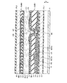
- FIG. 3 is a schematic cross-sectional view of the display device according to the present embodiment.
- FIG. 4 is a schematic diagram of the configuration of the display device according to the present embodiment.
- FIG. 5 is a schematic diagram showing an example of the aging process.
- FIG. 6 is a schematic diagram showing an example of the aging process.
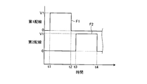
- FIG. 7 is a graph showing an example of the output timing of the gate signal.
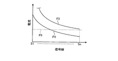
- FIG. 8 is a graph showing an example of the current value flowing through the signal line.
- FIG. 1 is a plan view schematically showing a display device according to the present embodiment.
- the display device 1 according to the present embodiment includes a first substrate SUB1 which is an array substrate and a second substrate SUB2 which is an opposing substrate.
- the direction parallel to the surfaces of the first substrate SUB1 and the second substrate SUB2 is referred to as the direction X.
- the direction parallel to the surfaces of the first substrate SUB1 and the second substrate SUB2 and intersecting the direction X here, the direction orthogonal to the direction X is defined as the direction Y.
- the direction toward one side of the direction Y is defined as the first direction Y1
- the direction toward the other side of the direction Y that is, the direction opposite to the first direction Y1
- the direction toward one side of the direction X is referred to as the third direction X1
- the direction toward the other side of the direction X that is, the direction opposite to the third direction X1
- the direction orthogonal to the direction X and the direction Y is defined as the direction Z.
- the first substrate SUB1 and the second substrate SUB2 are laminated in the direction Z.
- the area of the first substrate SUB1 is larger than that of the second substrate SUB2.
- the first substrate SUB1 is laminated so that the portion on the first direction Y1 side projects from the second substrate SUB2 on the first direction Y1 side when viewed from the direction Z. That is, the display device 1 has a superposed region AR1 on which the first substrate SUB1 and the second substrate SUB2 overlap, and an overhang region AR2 in which the second substrate SUB2 is not provided and only the first substrate SUB1 is provided. There is.
- the overhanging region AR2 is adjacent to the overlapping region AR1 on the Y1 side in the first direction.
- the display device 1 has a display area A and a peripheral area B.
- the display area A is an area in which a plurality of pixels are arranged and an image is displayed.
- the peripheral area B is an area in which pixels are not arranged and an image is not displayed.
- the peripheral area B is an area outside the display area A when viewed from the Z direction.
- the peripheral area B has a frame shape surrounding the display area A and can be said to be a frame area.
- the display area A is provided in the superposed area AR1 on which the first substrate SUB1 and the second substrate SUB2 overlap.
- the peripheral region B is an region within the first substrate SUB1. Further, a part of the peripheral area B is provided in the superposed area AR1 and the other part is provided in the overhanging area AR2.
- the peripheral region B is provided from the superposed region AR1 to the overhanging region AR2. Therefore, it can be said that the first substrate SUB1 has a display area A and a peripheral area B, and further, it can be said that the first substrate SUB1 is divided into a display area A and a peripheral area B.
- the peripheral area B includes a first peripheral area B1, a second peripheral area B2, a third peripheral area B3, and a fourth peripheral area B4.
- the first peripheral area B1 is a peripheral area B on the first direction Y1 side of the display area A.
- the second peripheral area B2 is a peripheral area B on the second direction Y2 side of the display area A, in other words, a peripheral area B on the opposite side of the first peripheral area B1 across the display area A.
- the third peripheral area B3 is a peripheral area B on the third direction X1 side of the display area A.
- the fourth peripheral region B4 is a peripheral region B on the fourth direction X2 side of the display region A, in other words, a peripheral region B on the opposite side of the third peripheral region B3 across the display region A.
- the first peripheral region B1 is provided from the superposed region AR1 to the overhanging region AR2 on the first direction Y1 side of the superposed region AR1. That is, the first peripheral region B1 includes an inner peripheral region B1a located in the superposed region AR1 and an outer peripheral region B1b located in the overhanging region AR2.
- the second peripheral region B2, the third peripheral region B3, and the fourth peripheral region B4 are located in the superposed region AR1. That is, the superimposed region AR1 is occupied by the display region A, the inner peripheral region B1a, the second peripheral region B2, the third peripheral region B3, and the fourth peripheral region B4, and the overhanging region AR2 is the outer peripheral region B1b. Is occupied by.
- a wiring board 101 is provided in the outer peripheral region B1b of the first peripheral region B1.
- the wiring board 101 is composed of, for example, a flexible wiring board (FPC: Flexible Printed Circuits).
- a driver IC (Integrated Circuit) 110 is provided on the wiring board 101.
- the driver IC 110 includes a control circuit, a detection circuit, an analog front end, and the like that control the display of the display device 1.
- the display device 1 may have a configuration that can be connected to the wiring board 101 and the driver IC 110, and the display device 1 may have a configuration that does not include the wiring board 101 and the driver IC 110. Further, the display device 1 may include the wiring board 101 and the driver IC 110.
- the display device 1 further has a plurality of driver terminals D provided in the peripheral area B and a plurality of inspection terminals T provided in the peripheral area B.
- the driver terminal D and the inspection terminal T are provided in the first peripheral region B1, and more specifically, are provided in the outer peripheral region B1b of the first peripheral region B1.
- the inspection terminal T is provided on the fourth direction X2 side of the driver terminal D in the example of FIG. 1, but is not limited thereto.
- the driver terminal D is a terminal that can be connected to the driver IC 110.
- the driver terminal D is a terminal for supplying various signals output from the connected driver IC 110 to the wiring of the display device 1.
- the inspection terminal T is a terminal for inspecting the wiring, here, performing the aging process. The aging process will be described later.
- FIG. 2 is a schematic diagram showing the pixel arrangement of the display device according to the present embodiment.
- the display device 1 includes a plurality of pixels PX in the display area A.
- the plurality of pixels PX are arranged side by side in a matrix in the direction X and the direction Y.
- the display device 1 has a plurality of wirings in the display area A.
- the display device 1 includes m scanning lines G (G1 to Gm), n signal lines S (S1 to Sn), and a common line CL as wiring provided in the display area A.
- m and n are any two or more integers.
- the scanning line G is connected to the gate driver GD.
- the signal required for the operation of the gate driver GD is supplied from the driver IC 110.
- the signal line S and the common line CL are connected to the driver IC 110.
- the scanning line G, the gate driver GD, the signal line S, and the common line CL are formed on the first substrate SUB1 shown in FIG.
- the pixel PX includes a switching element W, a pixel electrode PE, a common electrode CE, and a liquid crystal layer LC.
- the switching element W is composed of, for example, a thin film transistor (TFT) and is electrically connected to a scanning line G and a signal line S.
- the pixel electrode PE is electrically connected to the switching element W.
- the common electrode CE is electrically connected to the common wire CL.
- the gate driver GD outputs a control signal for making the switching element W connected to the scanning line G conductive to the scanning line G.
- the driver IC 110 outputs a video signal to the signal line S while the switching element W is in a conductive state. As a result, a desired pixel potential is written in the pixel electrode PE. Further, the driver IC 110 supplies a common potential to the common line CL. As a result, the common electrode CE becomes a common potential.
- each of the pixel electrode PEs faces the common electrode CE, and the liquid crystal layer LC is driven by an electric field generated by the potential difference between the pixel potential of the pixel electrode PE and the common potential of the common electrode CE.
- the holding capacitance CS is formed, for example, between an electrode having the same potential as the common electrode CE and an electrode having the same potential as the pixel electrode PE.
- FIG. 3 is a schematic cross-sectional view of the display device according to the present embodiment.
- the first substrate SUB1 includes an insulating substrate 10, insulating layers 11, 12, 13, 14, 15, lower light-shielding layer US, semiconductor layer SC, scanning line G, signal line S, connection electrode RE, common electrode CE, and pixel electrode. It is provided with PE and an alignment film AL1.
- the insulating substrate 10 is a transparent substrate such as a glass substrate or a resin substrate.
- the lower light-shielding layer US is located between the insulating substrate 10 and the insulating layer 11. In the example of FIG.
- the lower light-shielding layer US is formed so as to overlap both gate electrodes, but may be formed so as to be separated from each other at each gate electrode.
- the semiconductor layer SC is located between the insulating layer 11 and the insulating layer 12.
- the semiconductor layer SC is formed of, for example, polycrystalline silicon, but may be formed of amorphous silicon or an oxide semiconductor.
- the two gate electrodes GE which are part of the scanning line G, are located between the insulating layer 12 and the insulating layer 13.
- the signal line S and the connection electrode RE are located between the insulating layer 13 and the insulating layer 14.
- the signal line S and the connection electrode RE are in contact with the semiconductor layer SC, respectively.
- the common electrode CE is located between the insulating layer 14 and the insulating layer 15.
- the pixel electrode PE is located between the insulating layer 15 and the alignment film AL1. A part of the pixel electrode PE faces the common electrode CE via the insulating layer 15.
- the common electrode CE and the pixel electrode PE are formed of a conductive material having translucency such as ITO (Indium Tin Oxide) and IZO (Indium Zinc Oxide).
- the pixel electrode PE is in contact with the connection electrode RE via the contact hole CH penetrating the insulating layers 14 and 15 at a position where it overlaps with the opening AP of the common electrode CE.
- the insulating layers 11 to 13 and the insulating layer 15 are transparent inorganic insulating layers such as silicon oxide, silicon nitride, and silicon oxynitride, and may have a single-layer structure or a multi-layer structure. There may be.
- the insulating layer 14 is a transparent organic insulating layer such as an acrylic resin.
- the second substrate SUB2 includes an insulating substrate 20, a light-shielding layer BM, a color filter layer CF, an overcoat layer OC, and an alignment film AL2.
- the insulating substrate 20 is a transparent substrate such as a glass substrate or a resin substrate.
- the light-shielding layer BM and the color filter layer CF are located between the insulating substrate 20 and the overcoat layer OC.
- the alignment film AL2 covers the overcoat layer OC.
- the liquid crystal layer LC is located between the first substrate SUB1 and the second substrate SUB2, and is held between the alignment film AL1 and the alignment film AL2.
- the liquid crystal layer LC is composed of a positive type (positive dielectric anisotropy) liquid crystal material or a negative type (negative dielectric anisotropy) liquid crystal material.
- the polarizing plate PL1 is arranged below the first substrate SUB1 (on the side opposite to the second substrate SUB2).
- the polarizing plate PL2 is arranged above the second substrate SUB2 (on the side opposite to the first substrate SUB1).
- a retardation plate, a scattering layer, an antireflection layer, and the like may be included if necessary.
- the illumination device IL is located below the polarizing plate PL1 (on the opposite side of the first substrate SUB1).
- the display device 1 is a liquid crystal display device in the lateral electric field mode, more specifically, the FFS (Fringe Field Switching) mode.
- the display device 1 is not limited to the FFS mode, and may be any display device such as the vertical electric field mode.
- the display device 1 has a configuration for performing an aging process for inspecting wiring.
- the aging process is a process performed before the display device 1 is shipped, and is a process of passing a current through the wiring to break the locally narrowed portion of the wiring and detect a defective portion of the wiring in advance. Is.
- the configuration for performing the aging process will be described below.
- FIG. 4 is a schematic diagram of the configuration of the display device according to the present embodiment.
- the driver terminal D included in the display device 1 is connected to the signal line S which is the wiring.
- the driver terminal D1 to the driver terminal Dn are connected to the signal line Sn from the signal line S1, respectively.
- a video line and a connection circuit may be provided between the driver terminal D and the signal line S.
- the connection circuit switches the connection between the video line and the signal line S, and further connects the video line to at least one signal line S selected from the plurality of signal lines S.
- the driver terminal D is connected to the signal line S. Therefore, when a signal is output from the driver IC 110 with the driver terminal D connected to the driver IC 110, the signal from the driver IC 110 is output to the signal line S as a video signal.
- the display device 1 has a first switch SW A and a second switch SW B in the first substrate SUB1.
- the first switch SW A and the second switch SW B are switching elements, in this case transistors.
- the display device 1 has a switch terminal TS and an output terminal T0 as inspection terminals T.
- the switch terminal TS is a terminal for outputting a gate signal to the first switch SW A and the second switch SW B.
- a plurality of switch terminals TS are provided. In the example of FIG. 4, as different switch terminal TS together, one total of three switch terminals T A, T B1, T B2 is provided.
- the output terminal T0 is a terminal for outputting a current for aging processing to the signal line S.
- a plurality of output terminals T0 are provided, and in the example of FIG. 4, a total of six output terminals T1, T2, T3, T4, T5, and T6 are provided.
- the number of switch terminals TS and output terminals T0 is not limited to those shown in FIG. 4, and may be arbitrary.
- the first switch SW A is provided in the outer peripheral region B1b of the first peripheral region B1, and in the outer peripheral region B1b, the side opposite to the display region A from the driver terminal D, that is, the first driver terminal D. It is provided on the direction Y1 side.
- a plurality of first switches SW A are provided. In the present embodiment, a total of q first switch SW A , from the first switch SW A1 to the first switch SW Aq , are provided.
- the number of the first switch SW A is arbitrary, but is preferably half the number of the signal lines S.
- the first switch SW A is connected to a plurality of driver terminals D, and is connected to two driver terminals D in the present embodiment. Since the driver terminal D is connected to the signal line S, it can be said that the first switch SW A is connected to a plurality of signal lines S, and in the present embodiment, it can be said that the first switch SW A is connected to two signal lines S. ..
- the drain electrode Dr is connected to one of the two driver terminals D (signal line S), and the source electrode So is connected to the other of the two driver terminals D (signal line S). It is connected.
- the first switch SW A is preferably connected to the end of the signal line S on the Y1 side in the first direction.
- the drain electrode Dr in the first switch SW A1 , is connected to the signal line S6 via the driver terminal D6, and the source electrode So is connected to the signal line S1 via the driver terminal D1. .. Further, in the first switch SW A2 , the drain electrode Dr is connected to the signal line S5 via the driver terminal D5, and the source electrode So is connected to the signal line S2 via the driver terminal D2. Further, in the first switch SW A3 , the drain electrode Dr is connected to the signal line S4 via the driver terminal D4, and the source electrode So is connected to the signal line S3 via the driver terminal D3.
- the drain electrode Dr is connected to the signal line S12 via the driver terminal D12, and the source electrode So is connected to the signal line S7 via the driver terminal D7.
- the drain electrode Dr is connected to the signal line S11 via the driver terminal D11, and the source electrode So is connected to the signal line S8 via the driver terminal D8.
- the drain electrode Dr is connected to the signal line S10 via the driver terminal D10, and the source electrode So is connected to the signal line S9 via the driver terminal D9.
- Subsequent first switch SW A is also connected to the signal line S in the same manner.
- such a connection relationship is an example. That is, the first switch SW A is connected to any two signal lines S, and the connected signal lines S may be different for each first switch SW A.
- Connection line L A is the point connected to the switch terminal T A, and extends toward the inside of the outer peripheral region B1b in a third direction X1.
- Connection line L A is in the outer peripheral region B1b, and is connected to the first switch SW A. More specifically, the connection line L A is connected to the gate electrode Ga of the first switch SW A. That is, the first switch SW A, the gate electrode Ga is connected to a switch terminal T A via the connection line L A.
- Connection line L A is connected to the gate electrode Ga of the plurality of first switch SW A. That is, the plurality of first switch SW A via the same connection line L A, are connected to the switch terminal T A. More, in this embodiment, all the first switch SW A, via the same connection line L A, are connected to the switch terminal T A.
- the drain electrode Dr is connected to one of the two driver terminals D, the source electrode So is connected to the other of the two driver terminals D, and the gate electrode Ga is connected. It is connected to the switch terminal T a via line L a. Accordingly, the first switch SW A, the current to the gate electrode Ga through the switch terminal T A (gate signal) is input, the two driver terminal D together, namely two signal lines S each other, electrical Connect to. On the other hand, the first switch SW A electrically cuts off (non-) the two driver terminals D, that is, the two signal lines S, in a state where no current (gate signal) is input to the gate electrode Ga. To connect).
- the first switch SW A is connected to the signal line S and the switch terminal T A, the gate signal from the switch terminal T A, configured to be capable of switching between blocking and the connection between the plurality of signal lines S Will be done.
- the connection line L A because they are connected to the plurality of first switch SW A, when the gate signal from the switch terminal T A is input, a gate signal to the gate electrode Ga of the plurality of first switch SW A input. Therefore, each of the plurality of first switches SW A connects the two signal lines S to each other.
- the output terminals T1, T2, T3, T4, T5, and T6 are connected to the connection lines L1, L2, L3, L4, L5, and L6, which are wirings, respectively.
- the connection lines L1, L2, L3, L4, L5, and L6 are connected to the output terminals T1, T2, T3, T4, T5, and T6 from the locations in the outer peripheral region B1b to the inner peripheral regions B1a and the fourth periphery. It extends to the second peripheral region B2 via the region B4 (or the third peripheral region B3), and extends within the second peripheral region B2 in the third direction X1. That is, it can be said that the output terminal T0 is connected to the connection line L0, and the connection line L0 extends to the second peripheral region B2.
- the second switch SW B is provided in the second peripheral region B2.
- the second switch SW B is connected to the connection line L0 and the signal line S. That is, the second switch SW B is connected to the output terminal T0 via the connection line L0. Further, it can be said that the second switch SW B is connected to the signal line S and is connected to the driver terminal D and the first switch SW A via the signal line S.
- the drain electrode Dr is connected to the output terminal T0 via the connection line L0.
- the source electrode So is connected to the signal line S.
- the second switch SW B is preferably connected to the end of the signal line S on the second direction Y2 side.
- a plurality of second switches SW B are provided, and in the example of FIG. 4, a total of n second switches SW B1 to SW Bn are provided.
- the number of second switches SW B is arbitrary, but is preferably the same as the number of signal lines S.
- the drain electrode Dr in the second switch SW B1 , the drain electrode Dr is connected to the connection line L1 and the source electrode So is connected to the signal line S1.
- the drain electrode Dr in the second switch SW B2 , the drain electrode Dr is connected to the connection line L2, and the source electrode So is connected to the signal line S2.
- the second switch SW B3 the drain electrode Dr is connected to the connection line L3, and the source electrode So is connected to the signal line S3.
- the drain electrode Dr is connected to the connection line L4, and the source electrode So is connected to the signal line S4.
- the drain electrode Dr is connected to the connection line L5, and the source electrode So is connected to the signal line S5.
- the drain electrode Dr is connected to the connection line L6, and the source electrode So is connected to the signal line S6.
- the drain electrode Dr is connected to the connection line L1 and the source electrode So is connected to the signal line S7.
- the drain electrode Dr is connected to the connection line L2, and the source electrode So is connected to the signal line S8.
- the drain electrode Dr is connected to the connection line L3, and the source electrode So is connected to the signal line S9.
- the drain electrode Dr is connected to the connection line L4, and the source electrode So is connected to the signal line S10.
- the drain electrode Dr is connected to the connection line L5, and the source electrode So is connected to the signal line S11.
- the drain electrode Dr is connected to the connection line L6, and the source electrode So is connected to the signal line S12.
- Subsequent second switches SW B are also connected to the connection line L0 and the signal line S in the same order.
- this connection relationship is also an example, and in the second switch SW B , if the drain electrode Dr is connected to any of the plurality of connection lines L0 and any of the plurality of signal lines S is connected to the source electrode So. Good.
- the second switch SW B is provided for each signal line S, and one second switch SW B is connected to one signal line S.
- the number of connection lines L0 is 6 in the example of this embodiment, which is smaller than the number of the second switch SW B and the signal line S. Therefore, it can be said that some of the second switch SW Bs have a common connection line L0 to be connected, in other words, a plurality of second switch SW Bs are connected to one connection line L0.
- the second switches SWB 1 , SWB 7 , ... Are connected to the connection line L1
- the second switches SWB 2 , SWB 8 , ... are connected to the connection line L2.
- the second switch SW B is connected to L0 every six, but it is not limited to being connected every six in this way.
- the switch terminal TB1 as the one-side terminal is connected to the first connection line LB1 .
- the first connection line L B1 from locations in the outer peripheral region B1b which is connected to the switch terminal T B1, through the inner peripheral region B1a, fourth peripheral region B4 (or the third peripheral area B3), a second peripheral It extends to the region B2 and extends within the second peripheral region B2 in the third direction X1.
- the first connection line L B1 is connected to a part of the second switch SW B among the plurality of second switch SW B in the second peripheral region B2. More specifically, the first connection line LB1 is connected to the gate electrode Ga of a part of the second switch SW B among the plurality of second switch SW B. That is, in some of the second switches SW B , the gate electrode Ga is connected to the switch terminal TB1 via the first connection line LB1 .
- the switch terminal TB2 as the other terminal is connected to the second connection line LB2 .
- the second connection line L B2 from the point in the outer peripheral region B1b which is connected to the switch terminal T B2, through the inner peripheral region B1a, fourth peripheral region B4 (or the third peripheral area B3), a second peripheral It extends to the region B2 and extends within the second peripheral region B2 in the third direction X1.
- the second connection line L B2, in the second peripheral region B2 is connected to a second switch SW B of another portion of the plurality of second switch SW B.
- the second connection line L B2 among the plurality of second switch SW B and is connected to a second switch SW B first connection line L B1 is not connected.
- the second connection line L B2 is connected to the gate electrode Ga of the second switch SW B to which the first connection line L B1 is not connected. That is, the second switch SW B of part of another of the plurality of second switch SW B, the gate electrode Ga is connected to a switch terminal T B2 via a second connection line L B2.
- the second switch SW B1 to the second switch SW B6 are connected to the first connection line LB1
- the second switch SW B7 to the second switch SW B14 are connected to the second connection line LB2 . It has been, and even after that, it has such a connection relationship. That is, when a plurality of adjacent (6 in FIG. 4) second switches SW B are grouped into one group, the connection lines connected to each group are different. That is, the first, third, ... groups are connected to the first connection line LB1 , and the second, fourth, ... groups are connected to the second connection line LB2. ..
- connection line is not limited to be different for each group in this way, and a part of the second switch SW B is connected to the first connection line LB1 and some other second switch SW B is second. Anything that is connected to the connection line LB2 may be used.
- the second switch SW B may be connection line are different for each one, of all of the second switch SW B, the second switch SW B half in the middle than in the third direction X1 side first 1 is connected to the connection line L B1, a second switch SW B half in the middle than in the fourth direction X2 side may be connected to the second connection line L B2.
- the drain electrode Dr is connected to the output terminal T0 via the connection line L0, and the source electrode So is connected to the signal line S.
- the gate electrode Ga is connected to the switch terminal TB1 via the first connection line LB 1
- the gate electrode Ga is connected to the second connection line. through L B2 and is connected to the switch terminal T B2.
- the second switch SW B connected to the first connection line LB1 will be referred to as a one-sided second switch SW BA
- the second switch SW B connected to the second connection line LB2 will be referred to as a second switch SW BA.
- the other side second switch SW BB The other side second switch SW BB .
- one side the second switch SW BA is configured to be switchable connection and disconnection between the output terminals T0 and the signal line S, the gate signal from the switch terminal T B1, the output terminal T0 and the signal line Switch connection and disconnection with S.
- the other side a second switch SW BB which is connected to the second connection line L B2 is the current (gate signal) is input to the gate electrode Ga through the second connection line L B2, a connection line L0
- the signal line S that is, the output terminal T0 and the signal line S are electrically connected.
- the other-side second switch SW BB in the state in which current to the gate electrode Ga through the second connection line L B2 (gate signal) is not input, the signal lines S and the connection line L0, that is, the output terminal The T0 and the signal line S are electrically cut off.
- the other side a second switch SW BB is configured to be switchable connection and disconnection between the output terminals T0 and the signal line S, the gate signal from the switch terminal T B2, the output terminal T0 and the signal line Switch connection and disconnection with S.
- the second switch SW B2 is connected to either the first connection line LB1 or the second connection line LB2 .
- the number of connection lines is not limited to two first connection line L B1 and the second connection line L B2, it may be three or more, in this case, their respective connection lines, a plurality of second A part of the switch SW B2 is connected.
- the display device 1 has the above configuration. Next, a method of inspecting the wiring of the display device 1, that is, an aging process will be described. 5 and 6 are schematic views showing an example of the aging process.
- the driver IC 110 is not connected to the driver terminal D, and the signal from the driver IC 110 is not input to the driver terminal D. However, if the signal from the driver IC 110 is not input to the driver terminal D, the driver IC 110 may be connected to the driver terminal D.
- the inspection device 200 when performing the aging process, the inspection device 200 is connected to the inspection terminal T.
- the inspection device 200 includes a control unit 201, a detection unit 202, a processing unit 203, and a drive circuit 204.
- the inspection device 200 is merely an example, and may not have some of these functions, and may have other functions.
- the driver IC 110 (see FIG. 1) may have a part of the functions of the inspection device 200.
- the control unit 201 is a circuit that controls the detection unit 202, the processing unit 203, and the drive circuit 204 to inspect the display device 1.
- the detection unit 202 is a circuit that detects a signal (here, current I) output from the signal line S.
- the detection unit 202 is, for example, a voltage detection circuit, a current detection circuit, or the like.
- the processing unit 203 is a determination circuit that determines a short circuit, disconnection, or the like of the signal line S based on the detection signal of the detection unit 202.
- the drive circuit 204 generates a gate signal for driving the switch and an inspection signal for passing a current I through the signal line S, and outputs the signal to the display device 1.
- the inspection device 200 outputs a gate signal to the switch terminal TS to drive the first switch SW A and the second switch SW B , thereby causing a current I to flow through the signal line S, and inspecting the signal line S, that is, aging. Perform processing.
- the inspection device 200 is connected to the inspection terminal T.
- inspection apparatus 200 from the drive circuit 204, the switch terminal T A, and outputs a gate signal.
- the gate signal is a current having a predetermined potential, and is preferably a constant fixed potential.
- Inspecting apparatus 200 for a predetermined period, i.e. the period of performing the aging treatment it continues to output the gate signal to the switch terminal T A.
- Gate signal output to the switch terminal T A via the connection line L A is input to the gate electrode Ga of each of the first switch SW A.
- Each of the first switch SW A connects the signal lines S to each other by inputting a gate signal to the gate electrode Ga.
- FIG. 7 is a graph showing an example of the output timing of the gate signal.
- the inspection device 200 outputs a gate signal to the switch terminal TB1 and the switch terminal TB2 in a time-division manner. That is, the inspection device 200 outputs a gate signal from the switch terminal TB1 to the first connection line LB1 in the first time, and in the second time different from the first time, the switch terminal TB2 to the second connection line LB1 .
- the gate signal is output to LB2 .
- the inspection device 200 applies the voltage V1 to the switch terminal TB1 in the first time between the time t1 and the time t2, so that the first connection line
- the gate signal is output to LB1 .
- the inspection device 200 stops the voltage application to the switch terminal TB2 in the first time between the time t1 and the time t2, so that the inspection device 200 gives a gate signal to the second connection line LB2 . Stops the output of. Then, as shown in the line segment F1, the inspection device 200 stops applying the voltage to the switch terminal TB1 in the second time between the time t3 and the time t4, so that the inspection device 200 connects to the first connection line LB1 . Stop the output of the gate signal.
- the inspection device 200 applies the voltage V1 to the switch terminal TB2 in the second time between the time t3 and the time t4, thereby causing a gate signal to the first connection line LB1. Is output.
- the inspection apparatus 200 in both the first hour and the second hour, continued output of the gate signal to the switch terminal T A.
- time t1 to time t4 are examples for explanation in FIG. 7.
- the time t3 may be the same time as the time t2.
- FIG. 5 shows the flow of the current I in the first time. Since the gate signal is output to the first connection line LB1 in the first time, the gate signal is input to the gate electrode Ga of the one-sided second switch SW BA connected to the first connection line LB1. Will be done.
- the second switch SW BA on the one side connects the connection line L0 and the signal line S, that is, the output terminal T0 and the signal line S by inputting a gate signal to the gate electrode Ga. Further, in the first time, since the gate is input to the gate electrode Ga of the first switch SW A , the signal lines S are connected to each other.
- a closed circuit is formed between the inspection device 200, the output terminal T0, the connection line L0, the second switch SW BA on one side, the signal line S, and the first switch SW A. It is formed.
- the inspection device 200, the output terminal T6, the connection line L6, the second switch SW B6 , the signal line S6, the first switch SW A1 , the signal line S1, and the second A closed circuit is formed between the switch SW B1 , the connection line L1, and the output terminal T1.
- a closed circuit is formed in the second switch SW B2, SW B3, SW B4, SW B5, etc., which is the second switch SW BA on one side, but the description thereof will be omitted.
- the first switch SW A and the one-sided second switch SW BA form a closed circuit.
- the gate signal is not input to the second connection line LB2 , the gate signal is input to the gate electrode Ga of the other side second switch SW BB connected to the second connection line LB2. Not done. Therefore, the second switch SW BB on the other side does not form a closed circuit.
- the inspection device 200 outputs an inspection signal from the drive circuit 204 to the output terminal T0.
- the inspection signal is a current having a predetermined potential.
- the inspection device 200 outputs inspection signals having different potentials to the paired output terminals T0.
- the inspection device 200 preferably outputs inspection signals having potentials having opposite polarities to the paired output terminals T0.
- the paired output terminals T0 refer to two output terminals T0 connected to each of the two signal lines S to which the same first switch SW A is connected. In the example of FIG. 5, for example, the output terminals T1 and It is an output terminal T6. In the example of FIG.
- the inspection device 200 outputs a positive polarity inspection signal to the output terminal T6 and outputs a negative polar potential inspection signal to the output terminal T1.
- the closed circuit is formed by the first switch SW A1 and the second switches SW B1 and SW B6 , the potential difference between the inspection signal at the output terminal T6 and the inspection signal at the output terminal T1 causes the output terminal T6.
- the current I flows from the connection line L6, the second switch SW B6 , the signal line S6, the first switch SW A1 , the signal line S1, the second switch SW B1 , the connection line L1, and the output terminal T1.
- the inspection device 200 causes a high voltage current I to flow by setting the potential difference between the output terminal T6 and the output terminal T1 as high as, for example, several tens of volts.
- the voltage value of the current I is set to be at least higher than the voltage of the video signal from the driver IC 110.
- the inspection device 200 may switch the polarities of the inspection signals output to the output terminal T1 and the output terminal T2 every predetermined time. As a result, the direction of the current I flowing at predetermined time intervals can be reversed.
- the current I also flows through the closed circuit formed by the second switch SW B2, SW B3, SW B4, SW B5, etc. , which is the other second switch SW BA on one side. That is, in the first time, the current I flows through the signal line S (signal line S1 to signal line S6, etc.) connected to the second switch SW BA on one side.
- the second switch SW BB other side does not form a closed circuit, to the signal line S which is connected to the other side a second switch SW BB (such as a signal line-S12 signal line S7), Current I does not flow.
- FIG. 6 shows the flow of the current I in the second time.
- the gate signal to the second connection line L B2 is output to the gate electrode Ga on the other side a second switch SW BB which is connected to the second connection line L B2, the gate signal is input Will be done.
- the second switch SW BB on the other side connects the connection line L0 and the signal line S, that is, the output terminal T0 and the signal line S by inputting a gate signal to the gate electrode Ga.
- the signal lines S are connected to each other.
- a closed circuit is formed between the inspection device 200, the output terminal T0, the connection line L0, the second switch SW BB on the other side, the signal line S, and the first switch SW A. It is formed.
- the inspection device 200, the output terminal T6, the connection line L6, the second switch SW B12 , the signal line S12, the first switch SW A4 , the signal line S7, and the second A closed circuit is formed between the switch SW B7 , the connection line L1, and the output terminal T1.
- a closed circuit is similarly formed in the second switch SW B8, SW B9, SW B10, SW B11, etc., which are the other second switch SW BB on the other side, but the description thereof will be omitted.
- the first switch SW A and the other side second switch SW BB form a closed circuit.
- the gate signal is not input to the first connection line LB1 , the gate signal is input to the gate electrode Ga of the one-sided second switch SW BA connected to the first connection line LB1. Not done. Therefore, the one-sided second switch SW BA does not form a closed circuit.
- the inspection device 200 outputs an inspection signal from the drive circuit 204 to the output terminal T0 in the second time as well as in the first time.
- the closed circuit is formed by the first switch SW A4 , the second switches SW B7 , and the SW B12 , the potential difference between the inspection signal at the output terminal T6 and the inspection signal at the output terminal T1 causes the output terminal T6.
- the current I also flows through the closed circuit formed by the second switch SW B8, SW B9, SW B10, SW B11, etc., which are the other second switch SW BB on the other side. That is, in the second time, the current I flows through the signal line S (signal line S7 to signal line S12, etc.) connected to the second switch SW BB on the other side. On the other hand, in the second time, since the second switch SW BA on one side does not form a closed circuit, the signal line S (signal line S1 to signal line S6, etc.) connected to the second switch SW BA on one side is used. Current I does not flow.
- the detection unit 202 and the processing unit 203 detect that no current or voltage is flowing to detect whether the signal line S is disconnected. It becomes possible. Further, for example, when a video signal is output to the signal line S in a lighting inspection after aging processing, the broken part is not displayed in color, so it is possible to detect whether the signal line S is broken by detecting it. it can.
- the inspection device 200 passes a current I through the signal line S (signal line S1 to signal line S6, etc.) connected to the second switch SW BA on one side in the first time, and causes the other side in the second time.
- a current I is passed through a signal line S (signal line S7 to signal line S12, etc.) connected to the second switch SW BB . That is, the inspection device 200 does not pass the current I through all the signal lines S at once, but switches the signal lines S through which the current I flows at each timing by time division.
- the number of wires through which the current flows increases, so that the potential is high on the downstream side of the current flow.
- the downstream side has a larger integrated value of resistance due to wiring or the like, so that the potential becomes lower. Therefore, when the aging inspection is performed, the current value flowing through the signal line S on the downstream side, that is, on the side far from the output terminal T0 becomes low. If the current value becomes low, the sub-disconnected portion of the signal line S cannot be appropriately disconnected, and the inspection accuracy may decrease. If the applied voltage at the output terminal T0 is increased, the current value of the signal line S on the downstream side can be increased, but if the applied voltage is too high, the load on the signal line S on the upstream side is high. It will be too much. Further, it is conceivable to increase the line width of the wiring such as the connection line L0 and the signal line S to reduce the resistance, but the wiring may become thick and the space may be insufficient.
- one side second switch SW BA which is a part of the second switch SW B , is connected to the first connection line LB 1, and some other second switch SW
- the other side second switch SW BB which is B , is connected to the second connection line LB2 . Therefore, during the aging process, the one-side second switch SW BA and the other-side second switch SW BB can be driven separately in a time-division manner, reducing the number of signal lines S through which current flows at one time. Can be done. As a result, the integrated value of the resistance can be reduced, the current value flowing through the signal line S can be suppressed from becoming too small, and the deterioration of the inspection accuracy can be suppressed.
- FIG. 8 is a graph showing an example of the current value flowing through the signal line.
- the line segment F0 in FIG. 8 is a preset current target value. It can be said that the current target value is a current value capable of appropriately disconnecting the sub-disconnection point. That is, if a current equal to or higher than the current target value is passed through all the signal lines S, it is possible to suppress a decrease in inspection accuracy.
- the current target value is, for example, 2 amperes, but can be set arbitrarily.
- the current value of the signal line S for example, the signal line Sn
- the current target value for example, the signal line Sn
- any second switch SW B and the first connection line L B1 and the second connection line L B2 It was connected to the Crab, which was driving the second switch SW B in a time-division manner.
- the first switch SW A may be time-division-driven instead of the second switch SW B.
- the closed circuit is not formed and the current I does not flow through the unconnected signal lines S. Therefore, even in this case, the number of signal lines S through which the current I flows at one time can be reduced.
- connection lines L A and a plurality of the first connection line and the second connecting line connects the portion of the first switch SW A to the first connecting line, the other Connect a part of the first switch SW A to the second connection line. Then, time-division driving is performed by passing a gate signal to the first connection line and the second connection line at different timings.
- all the second switches SW B may be connected to one connection line so that the second switch SW B is always driven.
- both the first switch SW A and the second switch SW B may be configured to be time-division-driven. That is, at least one of the first switch SW A and the second switch SW B , a part is connected to the switch terminal TS via the first wiring, and the other part is connected to the switch terminal TS via the second wiring. It suffices if it is done.
- the display device 1 includes a first substrate SUB1, a plurality of signal lines S (wiring), a plurality of switch terminals TS, a plurality of first switch SW A, and a plurality of first switches SW A. It has a second switch SW B.
- the first substrate SUB1 has a display area A in which a plurality of pixels PX are provided, and a peripheral area B outside the display area A.
- the signal line S is provided in the display area A and is connected to the pixel PX to supply a video signal to the pixel.
- the switch terminal TS is provided in the peripheral region B.
- the first switch SW A provided on the first peripheral area B1 of the first direction Y1 side of the display area A, the switch terminal TS (switch terminal T A in this case), and is connected to the signal line S.
- the second switch SW B is displayed is provided on the second peripheral area B2 in the second direction Y2 side of the area A, the switch terminal TS that is different from the switch terminal T A which is connected to the first switch SW A (switch terminal here It is connected to TB1 or switch terminal TB2 ) and signal line S.
- At least one of the first switch SW A and the second switch SW B is partially connected to the switch terminal TS via the first connection line, and the other part is connected to the switch terminal TS via the second connection line. Will be done.
- the first switch SW A and the second switch SW B is separately connected to the first connection line and the second connection line. Therefore, according to this display device 1, the first switch SW A or the second switch SW B can be driven in a time-division manner, and when the signal line S is inspected, the signal line S through which the current I flows at one time The number can be reduced. Therefore, it is possible to prevent the current value flowing through the signal line S from becoming too small at the time of inspection, and to suppress a decrease in reliability.
- the plurality of second switch SW B in part, connected to the switch terminal TS via a first connection line L B1, another part, the switch terminal TS via a second connection line L B2 Be connected. Further, the plurality of first switch SW A is connected to the switch terminal T A via the same connection line L A.
- the second switch SW B on the second peripheral region B2 side is multi-system, and the first switch SW A on the first peripheral region B1 side near the terminal is integrated into one system. As a result, while enabling time-division driving by the second switch SW B , it is possible to suppress the circuit of the first peripheral region B1 from becoming large and secure the space of the first peripheral region B1.
- a part of the plurality of second switches SW B is connected to the switch terminal TB1 (one side terminal) which is one of the plurality of switch terminals TS via the first connection line LB1 and the other. Is connected to the switch terminal TB2 (the other terminal) which is the other one of the plurality of switch terminals TS via the second connection line LB2 . Since the display device 1 connects the second switch SW B to another estimation terminal, it is possible to suitably perform time division drive at the time of inspection of the signal line S, and it is possible to suppress a decrease in reliability. .. In the present embodiment, thus, in the first connection line L B1 and the second connection line L B2, it is connected a different switch terminal T B1, T B2 each other.
- first connection line LB1 and the second connection line LB2 may be connected to the same switch terminal TS.
- the first connection line LB1 and the second connection line LB2 may be provided with a switch for switching between connection and non-connection to the switch terminal TS. Then, if you want to drive the second switch SW B2 connected to the first connection line L B1 is disconnected the switch terminal TS and the second connection line L B2 switch terminal TS and the first connection line L B1 as connection state As a state, a gate signal may be output from the switch terminal TS.
- a gate signal may be output from the switch terminal TS.
- the first switch SW A is the signal from the switch terminal T A, configured to be capable of switching between blocking and the connection between the plurality of signal lines S. According to this display device 1, by making it possible to connect a plurality of signal lines S to each other, it is possible to detect a sub-disconnection of a plurality of signal lines S in one aging process.
- the display device 1 further has an output terminal T0 provided in the peripheral region B and connected to the second switch SW B.
- the second switch SW B switches the connection and disconnection between the output terminal T0 and the signal line S by the gate signal from the switch terminal TS. According to this display device 1, the sub-disconnection of the signal line S can be suitably detected.
- a gate signal is output to the switch terminal TS to drive the first switch SW A and the second switch SW B , whereby a current I is passed through the signal line S.
- the signal line S is inspected.
- a gate signal is output to the switch terminal TS to the first connection line LB1 in the first time, a current I is passed through a part of the plurality of signal lines S in the first time, and the first time different second time by outputting a gate signal to the second connection line L B2 from the switch terminal TS in, electric current I to another part of the plurality of signal lines S at the second time.
- Display device 110 Driver IC A display region B surrounding area B1 first peripheral area B1a inner peripheral region B1b outer peripheral region D driver terminal L B1 first connection line L B2 second connecting line T A, T B1, T B2 , TS switch terminal T0 output terminal PX Pixel S signal line (wiring) SUB1 1st board SUB2 2nd board SW A 1st switch SW B 2nd switch Y1 1st direction Y2 2nd direction
Landscapes
- Physics & Mathematics (AREA)
- General Physics & Mathematics (AREA)
- Nonlinear Science (AREA)
- Engineering & Computer Science (AREA)
- Theoretical Computer Science (AREA)
- Mathematical Physics (AREA)
- Chemical & Material Sciences (AREA)
- Crystallography & Structural Chemistry (AREA)
- Optics & Photonics (AREA)
- Liquid Crystal (AREA)
- Microelectronics & Electronic Packaging (AREA)
- Devices For Indicating Variable Information By Combining Individual Elements (AREA)
Abstract
表示装置(1)は、表示領域(A)、及び表示領域(A)よりも外側の周辺領域(B)を有する第1基板(SUB1)と、表示領域(A)に設けられて、画素に信号を供給する配線と、周辺領域Bに設けられる端子である複数のスイッチ端子(TS)と、表示領域Aの第1方向(Y1)側の第1周辺領域(B1)に設けられ、スイッチ端子(TS)及び配線に接続される複数の第1スイッチ(SWA)と、表示領域(A)の第2方向(Y2)側の第2周辺領域(B2)に設けられ、第1スイッチ(SWA)に接続されるスイッチ端子(TS)とは異なるスイッチ端子(TS)、及び配線に接続される複数の第2スイッチ(SWB)と、を有する。第1スイッチ(SWA)及び第2スイッチ(SWB)の少なくとも一方は、一部が第1接続線(LB1)を介してスイッチ端子(TS)に接続され、他の一部が第2接続線(LB2)を介してスイッチ端子(TS)に接続される。
Description
本発明は、表示装置及び検査方法に関する。
表示装置の信頼性を確保するために、表示装置を検査する技術が種々検討されている。例えば特許文献1には、表示装置に、画素に接続された信号線に接続される検査用端子を設ける旨が記載されている。特許文献1によると、検査用端子から検査用データ信号を入力することで、画素に検査用データ信号に応じた発色を行わせて、発色状態の検査を行う。
近年では、表示装置の高精細化に伴い、配線の本数が増加し各配線が細線化される傾向にあり、局所的に線幅が細くなる配線が製造されることが考えられる。このような表示装置は、駆動時間の経過に伴い駆動電流が流れる積算時間が長くなると、配線の局所的に線幅が細くなる箇所が、駆動電流のストレスに起因して断線するおそれがある。また、このように局所的に線幅が細くなる箇所以外にも、断線のおそれがあったり断線したりしている箇所を検出することも求められる。従って、断線のおそれがある箇所などがあるかを検出可能にしておくことで、信頼性の低下を抑制することが求められている。
本発明は、上記の課題に鑑みてなされたもので、信頼性の低下を抑制することが可能な表示装置及び検査方法を提供することを目的とする。
本発明の一態様による表示装置は、複数の画素が設けられる表示領域、及び前記表示領域よりも外側の周辺領域を有する第1基板と、前記表示領域に設けられて、前記画素に接続されて前記画素に信号を供給する複数の配線と、前記周辺領域に設けられる端子である複数のスイッチ端子と、前記表示領域の第1方向側の前記周辺領域である第1周辺領域に設けられ、前記スイッチ端子、及び前記配線に接続される複数の第1スイッチと、前記表示領域の前記第1方向と反対方向の第2方向側の前記周辺領域である第2周辺領域に設けられ、前記第1スイッチに接続される前記スイッチ端子とは異なる前記スイッチ端子、及び前記配線に接続される複数の第2スイッチと、を有し、前記第1スイッチ及び前記第2スイッチの少なくとも一方は、一部が第1接続線を介して前記スイッチ端子に接続され、他の一部が第2接続線を介して前記スイッチ端子に接続される。
本発明の一態様による検査方法は、前記表示装置の検査方法であって、前記スイッチ端子に信号を出力して前記第1スイッチ及び前記第2スイッチを駆動させることで、前記配線に電流を流して前記配線の検査を行う際に、第1時間において前記スイッチ端子から前記第1接続線へ前記信号を出力することで、前記第1時間において複数の前記配線のうちの一部に電流を流し、前記第1時間と異なる第2時間において前記スイッチ端子から前記第2接続線へ前記信号を出力することで、前記第2時間において複数の前記配線のうちの他の一部に電流を流す。
以下に、本発明の各実施形態について、図面を参照しつつ説明する。なお、開示はあくまで一例にすぎず、当業者において、発明の主旨を保っての適宜変更について容易に想到し得るものについては、当然に本発明の範囲に含有されるものである。また、図面は説明をより明確にするため、実際の態様に比べ、各部の幅、厚さ、形状等について模式的に表される場合があるが、あくまで一例であって、本発明の解釈を限定するものではない。また、本明細書と各図において、既出の図に関して前述したものと同様の要素には、同一の符号を付して、詳細な説明を適宜省略することがある。
(表示装置の構成)
図1は、本実施形態に係る表示装置を模式的に示す平面図である。図1に示すように、本実施形態に係る表示装置1は、アレイ基板である第1基板SUB1と、対向基板である第2基板SUB2とを備えている。以下、第1基板SUB1及び第2基板SUB2の表面に平行な方向を、方向Xとする。また、第1基板SUB1及び第2基板SUB2の表面に平行な方向であって、方向Xと交差する方向、ここでは方向Xと直交する方向を、方向Yとする。また、方向Yのうちの一方側に向かう方向を、第1方向Y1とし、方向Yのうちの他方側に向かう方向、すなわち第1方向Y1と反対方向を、第2方向Y2とする。同様に、方向Xのうちの一方側に向かう方向を、第3方向X1とし、方向Xのうちの他方側に向かう方向、すなわち第3方向X1と反対方向を、第4方向X2とする。また、方向X及び方向Yに直交する方向、すなわち第1基板SUB1及び第2基板SUB2の表面に直交する方向を、方向Zとする。
図1は、本実施形態に係る表示装置を模式的に示す平面図である。図1に示すように、本実施形態に係る表示装置1は、アレイ基板である第1基板SUB1と、対向基板である第2基板SUB2とを備えている。以下、第1基板SUB1及び第2基板SUB2の表面に平行な方向を、方向Xとする。また、第1基板SUB1及び第2基板SUB2の表面に平行な方向であって、方向Xと交差する方向、ここでは方向Xと直交する方向を、方向Yとする。また、方向Yのうちの一方側に向かう方向を、第1方向Y1とし、方向Yのうちの他方側に向かう方向、すなわち第1方向Y1と反対方向を、第2方向Y2とする。同様に、方向Xのうちの一方側に向かう方向を、第3方向X1とし、方向Xのうちの他方側に向かう方向、すなわち第3方向X1と反対方向を、第4方向X2とする。また、方向X及び方向Yに直交する方向、すなわち第1基板SUB1及び第2基板SUB2の表面に直交する方向を、方向Zとする。
第1基板SUB1と第2基板SUB2とは、方向Zに積層されている。第1基板SUB1は、第2基板SUB2よりも面積が広い。第1基板SUB1は、方向Zから見て、第1方向Y1側の部分が、第2基板SUB2よりも第1方向Y1側に突出するように積層されている。すなわち、表示装置1は、第1基板SUB1と第2基板SUB2とが重畳する重畳領域AR1と、第2基板SUB2が設けられず第1基板SUB1のみが設けられる張出領域AR2とを有している。張出領域AR2は、重畳領域AR1の第1方向Y1側に隣接する。
表示装置1は、表示領域Aと周辺領域Bとを有する。表示領域Aは、複数の画素が配置されて画像が表示される領域である。周辺領域Bは、画素が配置されずに画像が表示されない領域である。周辺領域Bは、Z方向から見た表示領域Aの外側の領域である。本実施形態では、周辺領域Bは、表示領域Aを囲う枠状であり、額縁領域ともいえる。表示領域Aは、第1基板SUB1と第2基板SUB2とが重畳する重畳領域AR1内に設けられている。周辺領域Bは、第1基板SUB1内の領域である。さらに言えば、周辺領域Bは、一部が重畳領域AR1内に設けられ、他の一部が張出領域AR2に設けられている。すなわち、周辺領域Bは、重畳領域AR1から張出領域AR2にわたって設けられている。従って、第1基板SUB1は、表示領域Aと周辺領域Bとを有するといえ、さらに言えば、表示領域Aと周辺領域Bとに区分けされているといえる。
周辺領域Bは、第1周辺領域B1と、第2周辺領域B2と、第3周辺領域B3と、第4周辺領域B4とを含む。第1周辺領域B1は、表示領域Aの第1方向Y1側の周辺領域Bである。第2周辺領域B2は、表示領域Aの第2方向Y2側の周辺領域Bであり、言い換えれば、表示領域Aを隔てて第1周辺領域B1の反対側にある周辺領域Bである。第3周辺領域B3は、表示領域Aの第3方向X1側の周辺領域Bである。第4周辺領域B4は、表示領域Aの第4方向X2側の周辺領域Bであり、言い換えれば、表示領域Aを隔てて第3周辺領域B3の反対側にある周辺領域Bである。
第1周辺領域B1は、重畳領域AR1から、重畳領域AR1より第1方向Y1側の張出領域AR2にわたって設けられている。すなわち、第1周辺領域B1は、重畳領域AR1内に位置する内側周辺領域B1aと、張出領域AR2内に位置する外側周辺領域B1bとを含んでいる。第2周辺領域B2、第3周辺領域B3、及び第4周辺領域B4は、重畳領域AR1内に位置している。すなわち、重畳領域AR1は、表示領域A、内側周辺領域B1a、第2周辺領域B2、第3周辺領域B3、及び第4周辺領域B4によって占められており、張出領域AR2は、外側周辺領域B1bによって占められている。
第1周辺領域B1の外側周辺領域B1bには、配線基板101が設けられている。配線基板101は、例えばフレキシブル配線基板(FPC:Flexible Printed Circuits)によって構成される。配線基板101には、ドライバIC(Integrated Circuit)110が設けられている。ドライバIC110は、表示装置1の表示を制御する制御回路、検出回路、アナログフロントエンド等を含む。なお、表示装置1は、配線基板101及びドライバIC110に接続可能な構成であればよく、配線基板101及びドライバIC110を含まない構成を表示装置1としてよい。また、配線基板101及びドライバIC110を含めて、表示装置1としてもよい。
表示装置1は、さらに、周辺領域Bに設けられた複数のドライバ端子Dと、周辺領域Bに設けられた複数の検査端子Tとを有する。本実施形態では、ドライバ端子D及び検査端子Tは、第1周辺領域B1に設けられ、さらに言えば、第1周辺領域B1の外側周辺領域B1bに設けられている。検査端子Tは、図1の例ではドライバ端子Dの第4方向X2側に設けられているが、それに限られない。
ドライバ端子Dは、ドライバIC110に接続可能な端子である。ドライバ端子Dは、接続されたドライバIC110から出力された各種信号を、表示装置1の配線に供給するための端子である。検査端子Tは、配線の検査、ここではエージング処理を行うための端子である。エージング処理については後述する。
図2は、本実施形態に係る表示装置の画素配列を示す模式図である。図2に示すように、表示装置1は、表示領域Aにおいて、複数の画素PXを備えている。複数の画素PXは、方向X及び方向Yにおいて、マトリクス状に並んで配置されている。また、表示装置1は、表示領域Aにおいて、複数の配線を有している。表示装置1は、表示領域Aに設けられる配線として、m本の走査線G(G1~Gm)と、n本の信号線S(S1~Sn)と、コモン線CLと、を備えている。なお、m及びnは、いずれの2以上の整数である。走査線Gは、ゲートドライバGDに接続されている。ゲートドライバGDの動作に必要な信号は、ドライバIC110から供給される。信号線S及びコモン線CLは、ドライバIC110に接続されている。走査線G、ゲートドライバGD、信号線S、及び、コモン線CLは、図1に示した第1基板SUB1に形成されている。
画素PXは、スイッチング素子W、画素電極PE、共通電極CE、及び液晶層LCを備えている。スイッチング素子Wは、例えば薄膜トランジスタ(TFT;Tin Film Transistor)によって構成され、走査線G及び信号線Sと電気的に接続されている。画素電極PEは、スイッチング素子Wと電気的に接続されている。共通電極CEは、コモン線CLと電気的に接続されている。
ゲートドライバGDは、走査線Gに接続されたスイッチング素子Wを導通状態とする制御信号を、走査線Gに出力する。ドライバIC110は、スイッチング素子Wが導通状態の期間に、信号線Sに映像信号を出力する。これにより、画素電極PEには、所望の画素電位が書き込まれる。また、ドライバIC110は、コモン線CLにコモン電位を供給する。これにより、共通電極CEは、コモン電位となる。各画素PXにおいて、画素電極PEの各々は、共通電極CEと対向しており、液晶層LCは、画素電極PEの画素電位と共通電極CEのコモン電位との電位差によって生じる電界によって駆動される。保持容量CSは、例えば、共通電極CEと同電位の電極、及び、画素電極PEと同電位の電極の間に形成される。
図3は、本実施形態に係る表示装置の模式的な断面図である。図3に示すように、表示装置1は、方向Zにおいて第1基板SUB1と第2基板SUB2とが積層されている。第1基板SUB1は、絶縁基板10、絶縁層11、12、13、14、15、下側遮光層US、半導体層SC、走査線G、信号線S、接続電極RE、共通電極CE、画素電極PE、及び、配向膜AL1を備えている。絶縁基板10は、ガラス基板や樹脂基板などの透明基板である。下側遮光層USは、絶縁基板10と絶縁層11との間に位置している。下側遮光層USは、図3の例では、両ゲート電極に跨って重畳するように形成されているが、ゲート電極毎に離間して形成されていてもよい。半導体層SCは、絶縁層11と絶縁層12との間に位置している。半導体層SCは、例えば、多結晶シリコンによって形成されているが、アモルファスシリコンや酸化物半導体によって形成されていてもよい。走査線Gの一部である2つのゲート電極GEは、絶縁層12と絶縁層13との間に位置している。信号線S及び接続電極REは、絶縁層13と絶縁層14との間に位置している。信号線S及び接続電極REは、それぞれ半導体層SCにコンタクトしている。共通電極CEは、絶縁層14と絶縁層15との間に位置している。画素電極PEは、絶縁層15と配向膜AL1との間に位置している。画素電極PEの一部は、絶縁層15を介して共通電極CEと対向している。共通電極CE及び画素電極PEは、ITO(Indium Tin Oxide)やIZO(Indium Zinc Oxide)などの透光性を有する導電材料によって形成されている。画素電極PEは、共通電極CEの開口部APと重畳する位置において、絶縁層14及び15を貫通するコンタクトホールCHを介して接続電極REに接触している。なお、絶縁層11乃至13、及び、絶縁層15は、シリコン酸化物、シリコン窒化物、シリコン酸窒化物などの透明な無機絶縁層であり、単層構造であってもよいし、多層構造であってもよい。絶縁層14は、アクリル樹脂などの透明な有機絶縁層である。
第2基板SUB2は、絶縁基板20、遮光層BM、カラーフィルタ層CF、オーバーコート層OC、及び、配向膜AL2を備えている。絶縁基板20は、ガラス基板や樹脂基板などの透明基板である。遮光層BM及びカラーフィルタ層CFは、絶縁基板20とオーバーコート層OCとの間に位置している。配向膜AL2は、オーバーコート層OCを覆っている。
液晶層LCは、第1基板SUB1及び第2基板SUB2の間に位置し、配向膜AL1と配向膜AL2との間に保持されている。液晶層LCは、ポジ型(誘電率異方性が正)の液晶材料、あるいは、ネガ型(誘電率異方性が負)の液晶材料によって構成されている。偏光板PL1は、第1基板SUB1の下方(第2基板SUB2と反対側)に配置されている。偏光板PL2は、第2基板SUB2の上方(第1基板SUB1と反対側)に配置されている。なお、偏光板PL1、PL2の他に、必要に応じて位相差板、散乱層、反射防止層などを含んでいてもよい。照明装置ILは、偏光板PL1の下方(第1基板SUB1と反対側)に位置している。
このように、図3の例では、表示装置1は、横電界モード、さらに言えばFFS(Fringe Field Switching)モードの液晶表示装置である。ただし、表示装置1は、FFSモードに限られず、縦電界モードなど、任意の表示装置であってよい。
表示装置1は、配線の検査のためのエージング処理を行うための構成を有している。エージング処理とは、表示装置1の出荷前に行う処理であり、配線に電流を流すことで、配線の局所的に線幅が細くなる箇所を断線させて、配線の不良箇所を予め検出する処理である。以下、エージング処理を行うための構成について説明する。
図4は、本実施形態に係る表示装置の構成の模式図である。図4に示すように、表示装置1が有するドライバ端子Dは、配線である信号線Sに接続されている。ドライバ端子D1からドライバ端子Dnは、それぞれ、信号線S1から信号線Snに接続されている。なお、図4では説明の便宜上省略しているが、ドライバ端子Dと信号線Sとの間には、ビデオ線と、接続回路とが設けられていてもよい。この場合、ドライバ端子Dとビデオ線と接続回路と信号線Sとは、この順で接続される。接続回路は、ビデオ線と信号線Sとの接続を切り替え、さらに言えば、複数の信号線Sのうち選択された少なくとも1つの信号線Sと、ビデオ線とを接続する。
このように、表示装置1は、ドライバ端子Dが信号線Sに接続されている。従って、ドライバ端子DがドライバIC110に接続された状態でドライバIC110から信号が出力されると、ドライバIC110からの信号は、映像信号として、信号線Sに出力される。
また、表示装置1は、第1基板SUB1内に、第1スイッチSWA及び第2スイッチSWBを有する。第1スイッチSWA及び第2スイッチSWBは、スイッチング素子、ここではトランジスタである。また、表示装置1は、検査端子Tとして、スイッチ端子TSと出力端子T0とを有する。スイッチ端子TSは、第1スイッチSWA及び第2スイッチSWBにゲート信号を出力するための端子である。スイッチ端子TSは、複数設けられている。図4の例では、互いに異なるスイッチ端子TSとして、スイッチ端子TA、TB1、TB2の合計3つが設けられている。また、出力端子T0は、信号線Sにエージング処理用の電流を出力するための端子である。出力端子T0は、複数設けられており、図4の例では、出力端子T1、T2、T3、T4、T5、T6の、合計6つ設けられている。ただし、スイッチ端子TS及び出力端子T0の数は図4に示すものに限られず任意であってよい。
第1スイッチSWAは、第1周辺領域B1の外側周辺領域B1b内に設けられており、外側周辺領域B1b内において、ドライバ端子Dよりも表示領域Aと反対側、すなわちドライバ端子Dの第1方向Y1側に設けられている。第1スイッチSWAは、複数設けられている。本実施形態では、第1スイッチSWAは、第1スイッチSWA1から第1スイッチSWAqの、合計q個設けられている。第1スイッチSWAの数は任意であるが、信号線Sの数の半分であることが好ましい。
第1スイッチSWAは、複数のドライバ端子Dに接続されており、本実施形態では、2つのドライバ端子Dに接続されている。ドライバ端子Dは信号線Sに接続されているため、第1スイッチSWAは、複数の信号線Sに接続されているといえ、本実施形態では2つの信号線Sに接続されているといえる。第1スイッチSWAは、ドレイン電極Drが、2つのドライバ端子D(信号線S)のうちの一方に接続され、ソース電極Soが、2つのドライバ端子D(信号線S)のうちの他方に接続されている。なお、第1スイッチSWAは、信号線Sの第1方向Y1側の端部に接続されていることが好ましい。
図4の例では、第1スイッチSWA1は、ドレイン電極Drがドライバ端子D6を介して信号線S6に接続されており、ソース電極Soがドライバ端子D1を介して信号線S1に接続されている。また、第1スイッチSWA2は、ドレイン電極Drがドライバ端子D5を介して信号線S5に接続されており、ソース電極Soがドライバ端子D2を介して信号線S2に接続されている。また、第1スイッチSWA3は、ドレイン電極Drがドライバ端子D4を介して信号線S4に接続されており、ソース電極Soがドライバ端子D3を介して信号線S3に接続されている。また、第1スイッチSWA4は、ドレイン電極Drがドライバ端子D12を介して信号線S12に接続されており、ソース電極Soがドライバ端子D7を介して信号線S7に接続されている。また、第1スイッチSWA5は、ドレイン電極Drがドライバ端子D11を介して信号線S11に接続されており、ソース電極Soがドライバ端子D8を介して信号線S8に接続されている。また、第1スイッチSWA6は、ドレイン電極Drがドライバ端子D10を介して信号線S10に接続されており、ソース電極Soがドライバ端子D9を介して信号線S9に接続されている。以降の第1スイッチSWAも、同様に信号線Sに接続されている。ただし、このような接続関係は一例である。すなわち、第1スイッチSWAは、任意の2つの信号線Sに接続されており、接続されている信号線Sが、第1スイッチSWA毎に異なればよい。
スイッチ端子TAは、接続線LAに接続されている。接続線LAは、スイッチ端子TAに接続されている箇所から、外側周辺領域B1b内を第3方向X1に向けて延在している。接続線LAは、外側周辺領域B1b内において、第1スイッチSWAに接続されている。より詳しくは、接続線LAは、第1スイッチSWAのゲート電極Gaに接続されている。すなわち、第1スイッチSWAは、ゲート電極Gaが、接続線LAを介してスイッチ端子TAに接続されている。接続線LAは、複数の第1スイッチSWAのゲート電極Gaのそれぞれに接続されている。すなわち、複数の第1スイッチSWAは、同じ接続線LAを介して、スイッチ端子TAに接続されている。さらに言えば、本実施形態では、全ての第1スイッチSWAが、同じ接続線LAを介して、スイッチ端子TAに接続されている。
このように、第1スイッチSWAは、ドレイン電極Drが2つのドライバ端子Dのうちの一方に接続され、ソース電極Soが2つのドライバ端子Dのうちの他方に接続され、ゲート電極Gaが接続線LAを介してスイッチ端子TAに接続されている。従って、第1スイッチSWAは、スイッチ端子TAを介してゲート電極Gaに電流(ゲート信号)が入力されると、2つのドライバ端子D同士を、すなわち2つの信号線S同士を、電気的に接続する。一方、第1スイッチSWAは、ゲート電極Gaに電流(ゲート信号)が入力されていない状態では、2つのドライバ端子D同士を、すなわち2つの信号線S同士)を、電気的に遮断(非接続に)する。このように、第1スイッチSWAは、信号線Sとスイッチ端子TAとに接続され、スイッチ端子TAからのゲート信号により、複数の信号線S同士の接続と遮断とを切り替え可能に構成される。なお、接続線LAは、複数の第1スイッチSWAに接続されているため、スイッチ端子TAからゲート信号が入力された場合、複数の第1スイッチSWAのゲート電極Gaにゲート信号を入力する。従って、複数の第1スイッチSWAのそれぞれが、2つの信号線S同士を接続する。
また、出力端子T1、T2、T3、T4、T5、T6は、それぞれ、配線である接続線L1、L2、L3、L4、L5、L6に接続されている。接続線L1、L2、L3、L4、L5、L6は、出力端子T1、T2、T3、T4、T5、T6に接続されている外側周辺領域B1b内の箇所から、内側周辺領域B1a、第4周辺領域B4(又は第3周辺領域B3)を経て、第2周辺領域B2まで延在し、第2周辺領域B2内を、第3方向X1に延在している。すなわち、出力端子T0は、接続線L0に接続されており、接続線L0が、第2周辺領域B2まで延在しているといえる。
第2スイッチSWBは、第2周辺領域B2内に設けられる。第2スイッチSWBは、接続線L0及び信号線Sに接続されている。すなわち、第2スイッチSWBは、接続線L0を介して出力端子T0に接続されている。また、第2スイッチSWBは、信号線Sに接続されており、信号線Sを介してドライバ端子D及び第1スイッチSWAに接続されているともいえる。具体的には、第2スイッチSWBは、ドレイン電極Drが、接続線L0を介して出力端子T0に接続されている。また、第2スイッチSWBは、ソース電極Soが、信号線Sに接続されている。なお、第2スイッチSWBは、信号線Sの第2方向Y2側の端部に接続されていることが好ましい。
第2スイッチSWBは、複数設けられており、図4の例では、第2スイッチSWB1からSWBnの、合計n個設けられている。第2スイッチSWBの数は任意であるが、信号線Sと同数であることが好ましい。図4の例では、第2スイッチSWB1は、ドレイン電極Drが接続線L1に接続され、ソース電極Soが信号線S1に接続されている。また、第2スイッチSWB2は、ドレイン電極Drが接続線L2に接続され、ソース電極Soが信号線S2に接続されている。第2スイッチSWB3は、ドレイン電極Drが接続線L3に接続され、ソース電極Soが信号線S3に接続されている。第2スイッチSWB4は、ドレイン電極Drが接続線L4に接続され、ソース電極Soが信号線S4に接続されている。第2スイッチSWB5は、ドレイン電極Drが接続線L5に接続され、ソース電極Soが信号線S5に接続されている。第2スイッチSWB6は、ドレイン電極Drが接続線L6に接続され、ソース電極Soが信号線S6に接続されている。また、第2スイッチSWB7は、ドレイン電極Drが接続線L1に接続され、ソース電極Soが信号線S7に接続されている。第2スイッチSWB8は、ドレイン電極Drが接続線L2に接続され、ソース電極Soが信号線S8に接続されている。第2スイッチSWB9は、ドレイン電極Drが接続線L3に接続され、ソース電極Soが信号線S9に接続されている。第2スイッチSWB10は、ドレイン電極Drが接続線L4に接続され、ソース電極Soが信号線S10に接続されている。第2スイッチSWB11は、ドレイン電極Drが接続線L5に接続され、ソース電極Soが信号線S11に接続されている。第2スイッチSWB12は、ドレイン電極Drが接続線L6に接続され、ソース電極Soが信号線S12に接続されている。以降の第2スイッチSWBも、同様の順番で、接続線L0と信号線Sとに接続されている。ただし、この接続関係も一例であり、第2スイッチSWBは、ドレイン電極Drが複数の接続線L0のいずれかに接続され、ソース電極Soに複数の信号線Sのいずれかが接続されればよい。
なお、第2スイッチSWBは、信号線S毎に設けられており、1つの信号線Sには1つの第2スイッチSWBが接続されているといえる。一方、接続線L0の数は、本実施形態の例では6本であり、第2スイッチSWB及び信号線Sの数より少ない。従って、一部の第2スイッチSWBは、接続される接続線L0が共通しており、言い換えれば、1つの接続線L0には、複数の第2スイッチSWBが接続されているといえる。図4では、接続線L1に第2スイッチSWB1、SWB7、・・・が接続され、接続線L2に第2スイッチSWB2、SWB8、・・・が接続されるなど、1つの接続線L0に対し第2スイッチSWBが6個おきに接続されているが、このように6個おきに接続されることに限られない。
一方側端子としてのスイッチ端子TB1は、第1接続線LB1に接続されている。第1接続線LB1は、スイッチ端子TB1に接続されている外側周辺領域B1b内の箇所から、内側周辺領域B1a、第4周辺領域B4(又は第3周辺領域B3)を経て、第2周辺領域B2まで延在し、第2周辺領域B2内を、第3方向X1に延在している。第1接続線LB1は、第2周辺領域B2内において、複数の第2スイッチSWBのうちの一部の第2スイッチSWBに接続されている。より詳しくは、第1接続線LB1は、複数の第2スイッチSWBのうちの一部の第2スイッチSWBの、ゲート電極Gaに接続されている。すなわち、一部の第2スイッチSWBは、ゲート電極Gaが、第1接続線LB1を介してスイッチ端子TB1に接続されている。
他方側端子としてのスイッチ端子TB2は、第2接続線LB2に接続されている。第2接続線LB2は、スイッチ端子TB2に接続されている外側周辺領域B1b内の箇所から、内側周辺領域B1a、第4周辺領域B4(又は第3周辺領域B3)を経て、第2周辺領域B2まで延在し、第2周辺領域B2内を、第3方向X1に延在している。第2接続線LB2は、第2周辺領域B2内において、複数の第2スイッチSWBのうちの他の一部の第2スイッチSWBに接続されている。言い換えれば、第2接続線LB2は、複数の第2スイッチSWBのうち、第1接続線LB1が接続されてない第2スイッチSWBに接続されている。第2接続線LB2は、第1接続線LB1が接続されてない第2スイッチSWBの、ゲート電極Gaに接続されている。すなわち、複数の第2スイッチSWBのうち他の一部の第2スイッチSWBは、ゲート電極Gaが、第2接続線LB2を介してスイッチ端子TB2に接続されている。
図4の例では、第2スイッチSWB1から第2スイッチSWB6までが第1接続線LB1に接続され、第2スイッチSWB7から第2スイッチSWB14までが第2接続線LB2に接続されており、以降でもこのような接続関係となっている。すなわち、隣接する複数(図4では6個)の第2スイッチSWBを1つのグループとした場合、グループ毎に接続される接続線が異なっている。すなわち、1つ目、3つ目、・・・のグループが第1接続線LB1に接続され、2つ目、4つ目、・・・のグループが第2接続線LB2に接続される。ただし、このようにグループ毎に接続線が異なることに限られず、一部の第2スイッチSWBが第1接続線LB1に接続されて、他の一部の第2スイッチSWBが第2接続線LB2に接続されるものであればよい。例えば、第2スイッチSWBは、1個毎に接続線が異なってもよいし、全ての第2スイッチSWBのうち、中央より第3方向X1側にある半数の第2スイッチSWBが第1接続線LB1に接続され、中央より第4方向X2側にある半数の第2スイッチSWBが第2接続線LB2に接続されてもよい。
このように、それぞれの第2スイッチSWBは、ドレイン電極Drが接続線L0を介して出力端子T0に接続され、ソース電極Soが信号線Sに接続される。また、一部の第2スイッチSWBは、ゲート電極Gaが第1接続線LB1を介してスイッチ端子TB1に接続され、他の第2スイッチSWBは、ゲート電極Gaが第2接続線LB2を介してスイッチ端子TB2に接続されている。以下、適宜、第1接続線LB1に接続されている第2スイッチSWBを、一方側第2スイッチSWBAと記載し、第2接続線LB2に接続されている第2スイッチSWBを、他方側第2スイッチSWBBと記載する。
第1接続線LB1に接続されている一方側第2スイッチSWBAは、第1接続線LB1を介してゲート電極Gaに電流(ゲート信号)が入力されると、接続線L0と信号線Sとを、すなわち出力端子T0と信号線Sとを、電気的に接続する。また、一方側第2スイッチSWBAは、第1接続線LB1を介してゲート電極Gaに電流(ゲート信号)が入力されていない状態では、接続線L0と信号線Sとを、すなわち出力端子T0と信号線Sとを、電気的に遮断する。このように、一方側第2スイッチSWBAは、出力端子T0と信号線Sとの接続及び遮断を切り替え可能に構成されており、スイッチ端子TB1からのゲート信号により、出力端子T0と信号線Sとの接続及び遮断を切り替える。
一方、第2接続線LB2に接続されている他方側第2スイッチSWBBは、第2接続線LB2を介してゲート電極Gaに電流(ゲート信号)が入力されると、接続線L0と信号線Sとを、すなわち出力端子T0と信号線Sとを、電気的に接続する。また、他方側第2スイッチSWBBは、第2接続線LB2を介してゲート電極Gaに電流(ゲート信号)が入力されていない状態では、接続線L0と信号線Sとを、すなわち出力端子T0と信号線Sとを、電気的に遮断する。このように、他方側第2スイッチSWBBは、出力端子T0と信号線Sとの接続及び遮断を切り替え可能に構成されており、スイッチ端子TB2からのゲート信号により、出力端子T0と信号線Sとの接続及び遮断を切り替える。
このように、第2スイッチSWB2は、第1接続線LB1及び第2接続線LB2のいずれかに接続されている。ただし、接続線の数は第1接続線LB1及び第2接続線LB2の2本に限られず、3本以上であってよく、この場合、それらの接続線のそれぞれに、複数の第2スイッチSWB2のうちの一部が接続される。
(検査方法)
表示装置1は、以上のような構成になっている。次に、表示装置1の配線の検査方法、すなわちエージング処理について説明する。図5及び図6は、エージング処理の一例を示す模式図である。エージング処理を行う場合、ドライバIC110がドライバ端子Dに接続されておらず、ドライバIC110からの信号がドライバ端子Dに入力されない。ただし、ドライバIC110からの信号がドライバ端子Dに入力されていなければ、ドライバIC110がドライバ端子Dに接続されていてもよい。
表示装置1は、以上のような構成になっている。次に、表示装置1の配線の検査方法、すなわちエージング処理について説明する。図5及び図6は、エージング処理の一例を示す模式図である。エージング処理を行う場合、ドライバIC110がドライバ端子Dに接続されておらず、ドライバIC110からの信号がドライバ端子Dに入力されない。ただし、ドライバIC110からの信号がドライバ端子Dに入力されていなければ、ドライバIC110がドライバ端子Dに接続されていてもよい。
図5に示すように、エージング処理を行う場合、検査端子Tに検査装置200が接続される。検査装置200は、制御部201と、検出部202と、処理部203と、駆動回路204とを含む。なお、検査装置200は、あくまで一例であり、これらの機能の一部を有していなくてもよく、他の機能を有していてもよい。検査装置200の機能の一部は、ドライバIC110(図1参照)が有していてもよい。
制御部201は、検出部202、処理部203、駆動回路204を制御して、表示装置1の検査を行う回路である。検出部202は、信号線Sから出力される信号(ここでは電流I)を検出する回路である。検出部202は、例えば、電圧検出回路、電流検出回路等である。処理部203は、検出部202の検出信号に基づいて、信号線Sの短絡、断線等の判定を行う判定回路である。駆動回路204は、スイッチを駆動するゲート信号と、信号線Sに電流Iを流すための検査信号とを生成して、表示装置1に出力する。
検査装置200は、スイッチ端子TSにゲート信号を出力して第1スイッチSWA及び第2スイッチSWBを駆動させることで、信号線Sに電流Iを流して、信号線Sの検査、すなわちエージング処理を行う。図5に示すように、エージング処理を行う場合、検査装置200は、検査端子Tに接続される。エージング処理を行う場合、検査装置200は、駆動回路204から、スイッチ端子TAに、ゲート信号を出力する。ゲート信号は、所定の電位を有する電流であり、一定の固定電位であることが好ましい。検査装置200は、所定の期間、すなわちエージング処理を行う期間、スイッチ端子TAにゲート信号を出力し続ける。スイッチ端子TAに出力されたゲート信号は、接続線LAを介して、それぞれの第1スイッチSWAのゲート電極Gaに入力される。それぞれの第1スイッチSWAは、ゲート電極Gaにゲート信号が入力されることで、信号線S同士を接続する。
図7は、ゲート信号の出力タイミングの一例を示すグラフである。検査装置200は、スイッチ端子TB1及びスイッチ端子TB2に、時分割でゲート信号を出力する。すなわち、検査装置200は、第1時間において、スイッチ端子TB1から第1接続線LB1へゲート信号を出力し、第1時間とは異なる第2時間において、スイッチ端子TB2から第2接続線LB2へゲート信号を出力する。図7の例では、検査装置200は、線分F1に示すように、時刻t1から時刻t2までの間の第1時間において、スイッチ端子TB1に電圧V1を印加することで、第1接続線LB1にゲート信号を出力する。検査装置200は、線分F2に示すように、時刻t1から時刻t2までの間の第1時間において、スイッチ端子TB2への電圧印加を停止することで、第2接続線LB2へゲート信号の出力を停止する。そして、検査装置200は、線分F1に示すように、時刻t3から時刻t4の間の第2時間において、スイッチ端子TB1への電圧印加を停止することで、第1接続線LB1へのゲート信号の出力を停止する。そして、検査装置200は、線分F2に示すように、時刻t3から時刻t4の間の第2時間において、スイッチ端子TB2に電圧V1を印加することで、第1接続線LB1にゲート信号を出力する。なお、検査装置200は、第1時間及び第2時間の両方において、スイッチ端子TAへのゲート信号の出力を続ける。また、時刻t1から時刻t4は、図7で説明するための一例である。例えば、時刻t3を時刻t2と同じ時刻としてもよい。
図5は、第1時間における電流Iの流れを示している。第1時間においては、第1接続線LB1にゲート信号が出力されているため、第1接続線LB1に接続される一方側第2スイッチSWBAのゲート電極Gaには、ゲート信号が入力される。一方側第2スイッチSWBAは、ゲート電極Gaにゲート信号が入力されることで、接続線L0と信号線Sとを、すなわち出力端子T0と信号線Sとを、接続する。また、第1時間においては、第1スイッチSWAのゲート電極Gaにゲート入力されるため、信号線S同士が接続される。そのため、第1時間においては、検査装置200と、出力端子T0と、接続線L0と、一方側第2スイッチSWBAと、信号線Sと、第1スイッチSWAとの間で、閉回路が形成される。例えば、図5に示すように、検査装置200と、出力端子T6と、接続線L6と、第2スイッチSWB6と、信号線S6と、第1スイッチSWA1と、信号線S1と、第2スイッチSWB1と、接続線L1と、出力端子T1との間で、閉回路が形成される。他の一方側第2スイッチSWBAである第2スイッチSWB2、SWB3、SWB4、SWB5などにおいても、同様に閉回路が形成されるが、説明を省略する。このように、第1時間においては、第1スイッチSWAと一方側第2スイッチSWBAとが閉回路を形成する。
一方、第1時間においては、第2接続線LB2にゲート信号が入力されないため、第2接続線LB2に接続される他方側第2スイッチSWBBのゲート電極Gaには、ゲート信号が入力されない。従って、他方側第2スイッチSWBBは、閉回路を形成しない。
さらに、検査装置200は、駆動回路204から、出力端子T0に検査信号を出力する。検査信号は、所定の電位の電流である。検査装置200は、対になる出力端子T0に、異なる電位の検査信号を出力する。検査装置200は、対になる出力端子T0に、互いに逆極性の電位の検査信号を出力することが好ましい。対になる出力端子T0とは、同じ第1スイッチSWAが接続されている2つの信号線Sのそれぞれに接続される2つの出力端子T0を指し、図5の例では、例えば出力端子T1及び出力端子T6である。図5の例では、検査装置200は、出力端子T6にプラス極性の電位の検査信号を出力し、出力端子T1にマイナス極性の電位の検査信号を出力する。上述のように、第1スイッチSWA1と第2スイッチSWB1、SWB6とにより閉回路が形成されるため、出力端子T6における検査信号と出力端子T1における検査信号との電位差により、出力端子T6から、接続線L6、第2スイッチSWB6、信号線S6、第1スイッチSWA1、信号線S1、第2スイッチSWB1、接続線L1、及び出力端子T1の流れで、電流Iが流れる。検査装置200は、出力端子T6と出力端子T1との間の電位差を、例えば数十ボルトなど高く設定することで、高電圧の電流Iを流す。電流Iの電圧値は、少なくとも、ドライバIC110からの映像信号の電圧よりも高く設定される。なお、検査装置200は、所定時間経過毎に、出力端子T1と出力端子T2とに出力する検査信号の極性を入れ替えてもよい。これにより、所定時間毎に流す電流Iの方向を逆にすることができる。
他の一方側第2スイッチSWBAである第2スイッチSWB2、SWB3、SWB4、SWB5などが形成する閉回路にも、電流Iが流れる。すなわち、第1時間においては、一方側第2スイッチSWBAに接続される信号線S(信号線S1から信号線S6など)に、電流Iが流れる。一方、第1時間においては、他方側第2スイッチSWBBが閉回路を形成しないため、他方側第2スイッチSWBBに接続される信号線S(信号線S7から信号線S12など)には、電流Iが流れない。
図6は、第2時間における電流Iの流れを示している。第2時間においては、第2接続線LB2にゲート信号が出力されているため、第2接続線LB2に接続される他方側第2スイッチSWBBのゲート電極Gaには、ゲート信号が入力される。他方側第2スイッチSWBBは、ゲート電極Gaにゲート信号が入力されることで、接続線L0と信号線Sとを、すなわち出力端子T0と信号線Sとを、接続する。また、第2時間においては、第1スイッチSWAのゲート電極Gaにゲート入力されるため、信号線S同士が接続される。そのため、第2時間においては、検査装置200と、出力端子T0と、接続線L0と、他方側第2スイッチSWBBと、信号線Sと、第1スイッチSWAとの間で、閉回路が形成される。例えば、図6に示すように、検査装置200と、出力端子T6と、接続線L6と、第2スイッチSWB12と、信号線S12と、第1スイッチSWA4と、信号線S7と、第2スイッチSWB7と、接続線L1と、出力端子T1との間で、閉回路が形成される。なお、他の他方側第2スイッチSWBBである第2スイッチSWB8、SWB9、SWB10、SWB11などにおいても、同様に閉回路が形成されるが、説明を省略する。このように、第2時間においては、第1スイッチSWAと他方側第2スイッチSWBBとが閉回路を形成する。
一方、第2時間においては、第1接続線LB1にゲート信号が入力されないため、第1接続線LB1に接続される一方側第2スイッチSWBAのゲート電極Gaには、ゲート信号が入力されない。従って、一方側第2スイッチSWBAは、閉回路を形成しない。
さらに、検査装置200は、第2時間においても、第1時間と同様に、駆動回路204から、出力端子T0に検査信号を出力する。上述のように、第1スイッチSWA4と第2スイッチSWB7、SWB12とにより閉回路が形成されるため、出力端子T6における検査信号と出力端子T1における検査信号との電位差により、出力端子T6、接続線L6、第2スイッチSWB12、信号線S12、第1スイッチSWA4、信号線S7、第2スイッチSWB7、接続線L1、及び出力端子T1の流れで、電流Iが流れる。他の他方側第2スイッチSWBBである第2スイッチSWB8、SWB9、SWB10、SWB11などが形成する閉回路にも、電流Iが流れる。すなわち、第2時間においては、他方側第2スイッチSWBBに接続される信号線S(信号線S7から信号線S12など)に、電流Iが流れる。一方、第2時間においては、一方側第2スイッチSWBAが閉回路を形成しないため、一方側第2スイッチSWBAに接続される信号線S(信号線S1から信号線S6など)には、電流Iが流れない。
エージング処理においては、このようにして信号線Sに電流Iを流すことにより、例えば信号線Sの亜断線箇所、すなわち局所的に線幅が細くなっている箇所があった場合に、その箇所を断線させることができる。出荷前に破断させておいて破断を検出することで、出荷後の断線を抑制して、信頼性を向上させることができる。なお、エージング処理において信号線Sが断線した場合、電流が流れなくなるため、検出部202及び処理部203によって電流や電圧が流れていないことを検出して、信号線Sが断線したかを検出することが可能となる。また例えば、エージング処理後の点灯検査などで信号線Sに映像信号を出力した場合に、断線した箇所は色表示されないため、それを検出することで信号線Sが断線したかを検出することもできる。
さらに、検査装置200は、第1時間において、一方側第2スイッチSWBAに接続される信号線S(信号線S1から信号線S6など)に電流Iを流し、第2時間においては、他方側第2スイッチSWBBに接続される信号線S(信号線S7から信号線S12など)に電流Iを流す。すなわち、検査装置200は、一度に全ての信号線Sに電流Iを流さずに、時分割によって、タイミング毎に電流Iを流す信号線Sを切り替える。ここで、出力端子T0からそれぞれの信号線Sに電流を流してエージング検査を行う場合、信号線Sなどの電流が流れる配線の本数が多くなるため、電流の流れの下流側においては、電位が低くなる。すなわち、下流側ほど、配線などによる抵抗の積算値が大きくなるため、電位が低くなる。従って、エージング検査を行う場合に、下流側、すなわち出力端子T0と遠い側の信号線Sに流れる電流値が低くなる。電流値が低くなると、信号線Sの亜断線箇所を適切に断線できず、検査精度が低下するおそれがある。出力端子T0での印加電圧を高くすれば、下流側の信号線Sの電流値を高くすることは可能であるが、印加電圧を高くし過ぎると、上流側の信号線Sへの負荷が高くなり過ぎてしまう。また、接続線L0や信号線Sなどの配線の線幅を大きくして抵抗を下げることも考えられるが、配線が太くなってしまいスペースが不足するおそれもある。
それに対し、本実施形態に係る表示装置1は、一部の第2スイッチSWBである一方側第2スイッチSWBAを第1接続線LB1に接続し、他の一部の第2スイッチSWBである他方側第2スイッチSWBBを第2接続線LB2に接続している。従って、エージング処理の際に、一方側第2スイッチSWBAと他方側第2スイッチSWBBとを時分割で別々に駆動させることが可能となり、一度に電流が流れる信号線Sの数を減らすことができる。これにより抵抗の積算値を小さくすることが可能となり、信号線Sに流れる電流値が小さくなり過ぎることを抑制して、検査精度の低下が抑制される。
図8は、信号線に流れる電流値の一例を示すグラフである。図8の線分F0は、予め設定された電流目標値である。電流目標値は、亜断線箇所を適切に断線可能な電流値であるといえる。すなわち、全ての信号線Sに電流目標値以上の電流を流せば、検査精度の低下を抑制することが可能となる。なお、電流目標値は、例えば2アンペアであるが、任意に設定可能である。ここで、線分FXに示すように、例えば全ての信号線Sに同時に電流を流した場合、出力端子T0から遠い側の信号線S(例えば信号線Snなど)の電流値が、電流目標値より低くなるおそれがある。それに対し、本実施形態のように時分割で駆動させて電流が流れる信号線Sの数を減らすことにより、線分F3に示すように、信号線Sの電流値を高くすることが可能となり、結果として、全ての信号線Sの電流値を電流目標値以上とすることも可能となる。さらに、時分割で駆動を切り替えることで、全ての信号線Sに電流を流すことができる。
なお、本実施形態では、全ての第1スイッチSWAが1本の接続線LAに接続されており、第2スイッチSWBが第1接続線LB1と第2接続線LB2とのいずれかに接続されており、これにより第2スイッチSWBを時分割駆動していた。ただし、第2スイッチSWBの代わりに第1スイッチSWAを時分割駆動してもよい。この場合、駆動されていない第1スイッチSWAに接続された信号線S同士が非接続となるため、閉回路が形成されずに、非接続の信号線Sに電流Iが流れなくなる。そのため、この場合であっても、一度に電流Iを流す信号線Sの数を減らすことができる。第1スイッチSWAを時分割駆動する場合、接続線LAを第1接続線と第2接続線との複数とし、一部の第1スイッチSWAを第1接続線に接続し、他の一部の第1スイッチSWAを第2接続線に接続する。そして、第1接続線と第2接続線とに異なるタイミングでゲート信号を流すことで時分割駆動する。第1スイッチSWAを時分割駆動する場合、第2スイッチSWBを常時駆動とするように、全ての第2スイッチSWBを一本の接続線に接続してもよい。ただし、第1スイッチSWAと第2スイッチSWBとの両方を時分割駆動可能なように構成してもよい。すなわち、第1スイッチSWAと第2スイッチSWBと少なくとも一方において、一部が第1配線を介してスイッチ端子TSに接続され、他の一部が第2配線を介してスイッチ端子TSに接続されていればよい。
以上説明したように、本実施形態に係る表示装置1は、第1基板SUB1と、複数の信号線S(配線)と、複数のスイッチ端子TSと、複数の第1スイッチSWAと、複数の第2スイッチSWBとを有する。第1基板SUB1は、複数の画素PXが設けられる表示領域A、及び表示領域Aよりも外側の周辺領域Bを有する。信号線Sは、表示領域Aに設けられて、画素PXに接続されて画素に映像信号を供給する。スイッチ端子TSは、周辺領域Bに設けられる。第1スイッチSWAは、表示領域Aの第1方向Y1側の第1周辺領域B1に設けられ、スイッチ端子TS(ここではスイッチ端子TA)、及び信号線Sに接続される。第2スイッチSWBは、表示領域Aの第2方向Y2側の第2周辺領域B2に設けられ、第1スイッチSWAに接続されるスイッチ端子TAとは異なるスイッチ端子TS(ここではスイッチ端子TB1又はスイッチ端子TB2)、及び信号線Sに接続される。第1スイッチSWA及び第2スイッチSWBの少なくとも一方は、一部が第1接続線を介してスイッチ端子TSに接続され、他の一部が第2接続線を介してスイッチ端子TSに接続される。
この表示装置1は、第1スイッチSWA及び第2スイッチSWBの少なくとも一方が、第1接続線と第2接続線とに分けて接続されている。従って、この表示装置1によると、第1スイッチSWA又は第2スイッチSWBを時分割で駆動することが可能となり、信号線Sの検査の際に、一度に電流Iを流す信号線Sの数を少なくすることができる。従って、検査時に信号線Sに流れる電流値が小さくなり過ぎることを抑制して、信頼性の低下を抑制することができる。
また、複数の第2スイッチSWBは、一部が、第1接続線LB1を介してスイッチ端子TSに接続され、他の一部が、第2接続線LB2を介してスイッチ端子TSに接続される。また、複数の第1スイッチSWAは、同じ接続線LAを介してスイッチ端子TAに接続される。この表示装置1は、第2周辺領域B2側の第2スイッチSWBを多系統化して、端子に近い第1周辺領域B1側の第1スイッチSWAを一系統にしている。これにより、第2スイッチSWBによって時分割駆動を可能にしつつ、第1周辺領域B1の回路が大きくなることを抑制して、第1周辺領域B1のスペース確保を可能としている。
また、複数の第2スイッチSWBは、一部が、第1接続線LB1を介して複数のスイッチ端子TSのうちの1つであるスイッチ端子TB1(一方側端子)に接続され、他の一部が、第2接続線LB2を介して複数のスイッチ端子TSのうちの他の1つであるスイッチ端子TB2(他方側端子)に接続される。この表示装置1は、第2スイッチSWBを別の推知端子に接続するため、信号線Sの検査時の時分割駆動を好適に行う事が可能となり、信頼性の低下を抑制することができる。なお、本実施形態では、このように、第1接続線LB1と第2接続線LB2とに、互いに異なるスイッチ端子TB1、TB2が接続される。ただし、第1接続線LB1と第2接続線LB2とは、同じスイッチ端子TSに接続されていてもよい。この場合、たとえば、第1接続線LB1と第2接続線LB2とに、スイッチ端子TSに対する接続と非接続とを切り替えるスイッチを設けてもよい。そして、第1接続線LB1に接続される第2スイッチSWB2を駆動したい場合は、スイッチ端子TSと第1接続線LB1を接続状態としてスイッチ端子TSと第2接続線LB2を非接続状態として、スイッチ端子TSからゲート信号を出力すればよい。また、第2接続線LB2に接続される第2スイッチSWB2を駆動したい場合は、スイッチ端子TSと第2接続線LB2を接続状態としてスイッチ端子TSと第1接続線LB1を非接続状態として、スイッチ端子TSからゲート信号を出力すればよい。
また、第1スイッチSWAは、スイッチ端子TAからの信号により、複数の信号線S同士の接続と遮断とを切り替え可能に構成される。この表示装置1によると、複数の信号線S同士を接続可能とすることで、一回のエージング処理で複数の信号線Sの亜断線を検出することができる。
また、表示装置1は、周辺領域Bに設けられて第2スイッチSWBに接続される出力端子T0をさらに有する。第2スイッチSWBは、スイッチ端子TSからのゲート信号により、出力端子T0と信号線Sとの接続及び遮断を切り替える。この表示装置1によると、信号線Sの亜断線を好適に検出することができる。
また、本実施形態に係る表示装置1の検査方法は、スイッチ端子TSにゲート信号を出力して第1スイッチSWA及び第2スイッチSWBを駆動させることで、信号線Sに電流Iを流して信号線Sの検査を行う。その際に、第1時間においてスイッチ端子TSから第1接続線LB1へゲート信号を出力することで、第1時間において複数の信号線Sのうちの一部に電流Iを流し、第1時間と異なる第2時間においてスイッチ端子TSから第2接続線LB2へゲート信号を出力することで、第2時間において複数の信号線Sのうちの他の一部に電流Iを流す。この検査方法によると、一度に電流Iを流す信号線Sの数を少なくすることができる。従って、信号線Sに流れる電流値が小さくなり過ぎることを抑制して、信頼性の低下を抑制することができる。
また、本実施形態において述べた態様によりもたらされる他の作用効果について本明細書記載から明らかなもの、又は当業者において適宜想到し得るものについては、当然に本発明によりもたらされるものと解される。
1 表示装置
110 ドライバIC
A 表示領域
B 周辺領域
B1 第1周辺領域
B1a 内側周辺領域
B1b 外側周辺領域
D ドライバ端子
LB1 第1接続線
LB2 第2接続線
TA、TB1、TB2、TS スイッチ端子
T0 出力端子
PX 画素
S 信号線(配線)
SUB1 第1基板
SUB2 第2基板
SWA 第1スイッチ
SWB 第2スイッチ
Y1 第1方向
Y2 第2方向
110 ドライバIC
A 表示領域
B 周辺領域
B1 第1周辺領域
B1a 内側周辺領域
B1b 外側周辺領域
D ドライバ端子
LB1 第1接続線
LB2 第2接続線
TA、TB1、TB2、TS スイッチ端子
T0 出力端子
PX 画素
S 信号線(配線)
SUB1 第1基板
SUB2 第2基板
SWA 第1スイッチ
SWB 第2スイッチ
Y1 第1方向
Y2 第2方向
Claims (6)
- 複数の画素が設けられる表示領域、及び前記表示領域よりも外側の周辺領域を有する第1基板と、
前記表示領域に設けられて、前記画素に接続されて前記画素に信号を供給する複数の配線と、
前記周辺領域に設けられる端子である複数のスイッチ端子と、
前記表示領域の第1方向側の前記周辺領域である第1周辺領域に設けられ、前記スイッチ端子、及び前記配線に接続される複数の第1スイッチと、
前記表示領域の前記第1方向と反対方向の第2方向側の前記周辺領域である第2周辺領域に設けられ、前記第1スイッチに接続される前記スイッチ端子とは異なる前記スイッチ端子、及び前記配線に接続される複数の第2スイッチと、
を有し、
前記第1スイッチ及び前記第2スイッチの少なくとも一方は、一部が第1接続線を介して前記スイッチ端子に接続され、他の一部が第2接続線を介して前記スイッチ端子に接続される、
表示装置。 - 複数の前記第2スイッチは、一部が、前記第1接続線を介して前記スイッチ端子に接続され、他の一部が、前記第2接続線を介して前記スイッチ端子に接続され、
複数の前記第1スイッチは、同じ接続線を介して前記スイッチ端子に接続される、請求項1に記載の表示装置。 - 複数の前記第2スイッチは、一部が、前記第1接続線を介して複数の前記スイッチ端子のうちの1つである一方側端子に接続され、他の一部が、前記第2接続線を介して複数の前記スイッチ端子のうちの他の1つである他方側端子に接続される、請求項2に記載の表示装置。
- 前記第1スイッチは、前記スイッチ端子からの信号により、複数の前記配線同士の接続と遮断とを切り替え可能に構成される、請求項1から請求項3のいずれか1項に記載の表示装置。
- 前記周辺領域に設けられて前記第2スイッチに接続される端子である出力端子をさらに有し、
前記第2スイッチは、前記スイッチ端子からの信号により、前記出力端子と前記配線との接続及び遮断を切り替える、請求項1から請求項4のいずれか1項に記載の表示装置。 - 請求項1から請求項5のいずれか1項に記載の表示装置の検査方法であって、
前記スイッチ端子に信号を出力して前記第1スイッチ及び前記第2スイッチを駆動させることで、前記配線に電流を流して前記配線の検査を行う際に、
第1時間において前記スイッチ端子から前記第1接続線へ前記信号を出力することで、前記第1時間において複数の前記配線のうちの一部に電流を流し、
前記第1時間と異なる第2時間において前記スイッチ端子から前記第2接続線へ前記信号を出力することで、前記第2時間において複数の前記配線のうちの他の一部に電流を流す、検査方法。
Applications Claiming Priority (2)
| Application Number | Priority Date | Filing Date | Title |
|---|---|---|---|
| JP2019055273A JP2020154251A (ja) | 2019-03-22 | 2019-03-22 | 表示装置及び検査方法 |
| JP2019-055273 | 2019-03-22 |
Publications (1)
| Publication Number | Publication Date |
|---|---|
| WO2020195076A1 true WO2020195076A1 (ja) | 2020-10-01 |
Family
ID=72558889
Family Applications (1)
| Application Number | Title | Priority Date | Filing Date |
|---|---|---|---|
| PCT/JP2020/002397 Ceased WO2020195076A1 (ja) | 2019-03-22 | 2020-01-23 | 表示装置及び検査方法 |
Country Status (2)
| Country | Link |
|---|---|
| JP (1) | JP2020154251A (ja) |
| WO (1) | WO2020195076A1 (ja) |
Citations (4)
| Publication number | Priority date | Publication date | Assignee | Title |
|---|---|---|---|---|
| JPH0318891A (ja) * | 1989-06-15 | 1991-01-28 | Matsushita Electron Corp | 画像表示装置の検査方法 |
| JP2003029296A (ja) * | 2001-07-13 | 2003-01-29 | Toshiba Corp | アレイ基板及びその検査方法並びに液晶表示装置 |
| JP2003121867A (ja) * | 2001-10-11 | 2003-04-23 | Samsung Electronics Co Ltd | ビジュアルインスペクション手段を備えた薄膜トランジスタ基板及びビジュアルインスペクション方法 |
| JP2019101261A (ja) * | 2017-12-04 | 2019-06-24 | 株式会社ジャパンディスプレイ | 表示装置 |
-
2019
- 2019-03-22 JP JP2019055273A patent/JP2020154251A/ja active Pending
-
2020
- 2020-01-23 WO PCT/JP2020/002397 patent/WO2020195076A1/ja not_active Ceased
Patent Citations (4)
| Publication number | Priority date | Publication date | Assignee | Title |
|---|---|---|---|---|
| JPH0318891A (ja) * | 1989-06-15 | 1991-01-28 | Matsushita Electron Corp | 画像表示装置の検査方法 |
| JP2003029296A (ja) * | 2001-07-13 | 2003-01-29 | Toshiba Corp | アレイ基板及びその検査方法並びに液晶表示装置 |
| JP2003121867A (ja) * | 2001-10-11 | 2003-04-23 | Samsung Electronics Co Ltd | ビジュアルインスペクション手段を備えた薄膜トランジスタ基板及びビジュアルインスペクション方法 |
| JP2019101261A (ja) * | 2017-12-04 | 2019-06-24 | 株式会社ジャパンディスプレイ | 表示装置 |
Also Published As
| Publication number | Publication date |
|---|---|
| JP2020154251A (ja) | 2020-09-24 |
Similar Documents
| Publication | Publication Date | Title |
|---|---|---|
| US11796878B2 (en) | Active matrix substrate and display panel | |
| JP7142756B2 (ja) | 表示装置 | |
| JP5690916B2 (ja) | ディスプレイ装置用アレイ基板 | |
| JP6962759B2 (ja) | 表示装置 | |
| KR102145390B1 (ko) | 정전기 방전 회로를 포함하는 표시 장치 | |
| US8780309B2 (en) | Mother panel of liquid crystal display and method of manufacturing liquid crystal display using the same | |
| CN104769657B (zh) | 有源矩阵基板和显示装置 | |
| WO2013011855A1 (ja) | アクティブマトリクス型表示装置 | |
| US11966132B2 (en) | Display device | |
| CN104969283A (zh) | 显示装置 | |
| JP2020012869A (ja) | 表示装置及び表示装置の基板 | |
| CN107664861A (zh) | 显示装置 | |
| US9431438B2 (en) | Display device and method for fabricating the same | |
| JP6983006B2 (ja) | 表示装置 | |
| JP2009098407A (ja) | 表示装置 | |
| CN205656393U (zh) | 一种阵列基板及显示面板 | |
| WO2020195076A1 (ja) | 表示装置及び検査方法 | |
| KR20150024680A (ko) | 액정표시장치 | |
| JP7217650B2 (ja) | 表示装置 | |
| JP7149209B2 (ja) | 表示装置及び検査方法 | |
| US8953111B2 (en) | Pixel array | |
| CN101504502B (zh) | 电光装置以及电子设备 |
Legal Events
| Date | Code | Title | Description |
|---|---|---|---|
| 121 | Ep: the epo has been informed by wipo that ep was designated in this application |
Ref document number: 20778528 Country of ref document: EP Kind code of ref document: A1 |
|
| NENP | Non-entry into the national phase |
Ref country code: DE |
|
| 122 | Ep: pct application non-entry in european phase |
Ref document number: 20778528 Country of ref document: EP Kind code of ref document: A1 |