WO2020189741A1 - Signal processing device and signal processing method - Google Patents
Signal processing device and signal processing method Download PDFInfo
- Publication number
- WO2020189741A1 WO2020189741A1 PCT/JP2020/012134 JP2020012134W WO2020189741A1 WO 2020189741 A1 WO2020189741 A1 WO 2020189741A1 JP 2020012134 W JP2020012134 W JP 2020012134W WO 2020189741 A1 WO2020189741 A1 WO 2020189741A1
- Authority
- WO
- WIPO (PCT)
- Prior art keywords
- signal
- fluorescent particles
- input
- unit
- optical
- Prior art date
Links
Images


Classifications
-
- G—PHYSICS
- G06—COMPUTING; CALCULATING OR COUNTING
- G06E—OPTICAL COMPUTING DEVICES; COMPUTING DEVICES USING OTHER RADIATIONS WITH SIMILAR PROPERTIES
- G06E3/00—Devices not provided for in group G06E1/00, e.g. for processing analogue or hybrid data
-
- G—PHYSICS
- G06—COMPUTING; CALCULATING OR COUNTING
- G06N—COMPUTING ARRANGEMENTS BASED ON SPECIFIC COMPUTATIONAL MODELS
- G06N20/00—Machine learning
Definitions
- the present invention relates to a signal processing device and a signal processing method.
- An object of the present invention is to provide a signal processing device in which a large-scale FRET path is physically mounted, and a signal processing method.
- the signal processing apparatus includes an optical energy network including a plurality of fluorescent particles and configured such that an energy transfer path through the plurality of fluorescent particles is autonomously and randomly determined, and the light.
- a signal input unit that excites at least a part of the plurality of fluorescent particles according to an input signal to be input to the energy network, and a signal input unit that excites some of the fluorescent particles, and then reads an optical signal from the photoenergy network. It includes a signal reading unit and an acquisition unit that acquires a calculation result by the optical energy network based on the optical signal read by the signal reading unit.
- the plurality of fluorescences are received in response to the input of the input signal to the optical energy network configured so that the energy transfer path by the plurality of fluorescent particles is determined autonomously and randomly.
- the optical signal is read from the optical energy network, and the calculation result by the optical energy network is acquired based on the read optical signal.
- signal processing can be executed using an optical energy network based on a large-scale FRET path.
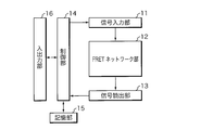
- FIG. 1 is a schematic diagram showing the configuration of the signal processing device according to the present embodiment
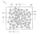
- FIG. 2 is a schematic diagram showing the configuration of the FRET network unit 12.
- the signal processing device according to the present embodiment is a device that performs calculations using an optical energy network in which signals are transmitted by FRET, and is a signal input unit 11, FRET network unit 12, signal reading unit 13, control unit 14, It includes a storage unit 15 and an input / output unit 16.
- the FRET network unit 12 is composed of nanostructures 120 in which a plurality of fluorescent particles 121, 121, ..., 121 are randomly arranged in a solid, a liquid, or an amorphous substance.
- the fluorescent particle 121 may be a fluorescent molecule or a fluorescent material that functions as a quantum dot.
- the nanostructure 120 may have a laminated structure. The number of fluorescent particles 121 arranged in the nanostructure 120 is adjusted so that the distance between adjacent fluorescent particles 121 and 121 is 10 nm or less. For example, volume is the nanostructures 120 of about 1 [mu] m 3 are disposed 106 about the fluorescent particles 121.
- Cy3 having an excitation peak of 550 nm and a fluorescence peak of 570 nm
- a fluorescence peak of 670 nm are used.
- the distance between any two fluorescent particles 121, 121 varies, but if the distance is about 10 nm or less, FRET can occur.
- the FRET generation condition is that not only the distance between the two fluorescent particles 121 and 121 but also the overlap between the emission spectrum on the donor side and the absorption spectrum on the acceptor side is large, and the two fluorescent particles 121 and 121 are appropriate. It is oriented, the fluorescence quantum yield on the donor side is large, and the absorption intensity of the acceptor is large.
- the path through which energy moves between the fluorescent particles 121 and 121 is determined autonomously and randomly. That is, the fluorescent particles 121, 121, ..., 121 in the nanostructure 120 construct an optical energy network through which signals are transmitted by FRET.
- the signal input unit 11 excites at least a part of the fluorescent particles 121, 121, ..., 121 according to the input signal.
- the input signal is a signal to be calculated in the signal processing device, may be generated inside the control unit 14, or may be input from the outside through the input / output unit 16.
- the signal input unit 11 controls the wavelength and time-series light intensity of the light to be irradiated to the nanostructure 120 according to the modulation parameters adjusted according to the input signal, and controls the wavelength and time-series light intensity (hereinafter referred to as light).
- Excitation light is applied to a specific irradiation region of the nanostructure 120.
- the modulation method is arbitrary, and it may be modulated according to a preset rule.
- the irradiation region for irradiating the excitation light is set in advance.
- the energy states of the fluorescent particles 121, 121, ..., 121 included in the irradiation region change from, for example, the ground state to the excited state.
- FRET is generated between the two fluorescent particles 121, 121 that satisfy the above conditions. That is, the excitation energy is transferred from the fluorescent particles 121 on the donor side to the fluorescent particles 121 on the acceptor side.
- Such FRET between the two fluorescent particles 121 and 121 is generated one after another in the fluorescent particles 121, 121, ..., 121 constituting the nanostructure 120. Therefore, after the excitation light is irradiated to the nanostructure 120 by the signal input unit 11, the energy states of the fluorescent particles 121, 121, ..., 121 constituting the nanostructure 120 are other fluorescent particles satisfying the generation conditions. It changes autonomously by FRET from 121, and changes to a state that represents the calculation result.
- the signal reading unit 13 After irradiating the excitation light from the signal input unit 11, the signal reading unit 13 irradiates the excitation light after the timing when the energy states of the fluorescent particles 121, 121, ..., 121 change to the states representing the calculation results (for example, irradiating the excitation light).
- the signal is read from the FRET network unit 12 (after the timing when about 10 to 12 seconds have passed since then).
- the signal reading unit 13 can read a signal from the FRET network unit 12 by performing wavelength decomposition measurement / time decomposition measurement using a spectroscope. As a method of reading a signal from the FRET network unit 12, a known method can be used.
- the reading region for the signal reading unit 13 to read the signal may be set to the entire region of the nanostructure 120, or a part of the region of the nanostructure 120 may be set.
- the signal read by the signal reading unit 13 is a signal of the fluorescence spectrum obtained from the fluorescent particles 121, 121, ..., 121 included in the reading region.
- the signal reading unit 13 outputs the signal read from the FRET network unit 12 to the control unit 14.
- the control unit 14 includes a CPU (Central Processing Unit), a ROM (Read Only Memory), a RAM (Random Access Memory), and the like.
- the CPU of the control unit 14 controls the operation of each hardware unit and executes various calculations by executing various computer programs stored in the ROM or the storage unit 15, and the entire device functions as the signal processing device of the present application. Let me.
- the RAM of the control unit 14 temporarily stores data and the like generated during execution of various computer programs.
- the calculation executed by the control unit 14 is a calculation for learning the relationship between the signal read by the signal reading unit 13 from the FRET network unit 12 and the calculation result by the FRET network unit 12, and the calculation using the result of the learning calculation is used for FRET. It includes an operation of deriving an operation result from a signal read by the network unit 12. These operations will be described in detail later.
- the control unit 14 is not limited to the above configuration, and may be any processing circuit including one or a plurality of CPUs, a multi-core CPU, a GPU (Graphics Processing Unit), a microcomputer, and the like. Further, the control unit 14 may have functions such as a clock for outputting date and time information, a timer for measuring the elapsed time from giving the measurement start instruction to giving the measurement end instruction, and a counter for counting the number.
- the storage unit 15 includes a storage device that uses a memory, an HDD (Hard Disk Drive), or the like.
- the storage unit 15 stores various computer programs executed by the control unit 14, data necessary for executing the computer programs, calculation results by the control unit 14, and the like.
- the computer program stored in the storage unit 15 is a learning program for learning the relationship between the signal read from the FRET network unit 12 by the signal reading unit 13 and the calculation result to be acquired as an output for the input signal, and the learning result. Based on this, it includes a calculation program for converting the signal read by the signal reading unit 13 from the FRET network unit 12 into a calculation result.
- the computer program stored in the storage unit 15 may be provided by a non-temporary recording medium in which the computer program is readablely recorded.
- the recording medium is, for example, a portable memory such as a CD-ROM, a USB memory, an SD (Secure Digital) card, a micro SD card, or a compact flash (registered trademark).
- the control unit 14 can read the computer program from the recording medium using a reading device (not shown), and install the read computer program in the storage unit 15.
- the computer program stored in the storage unit 15 may be provided by communication. In this case, the control unit 14 can acquire a computer program by communicating with an external server (not shown), and can install the acquired computer program in the storage unit 15.
- the input / output unit 16 includes an interface for inputting / outputting various information.
- the input / output unit 16 includes an interface for connecting an input device such as a keyboard and a mouse, and may receive a user's instruction through the connected input device.
- the input / output unit 16 includes an interface for connecting an external computer, and a signal output from the connected external computer may be input.
- the input / output unit 16 may include an interface for connecting an output device such as a liquid crystal display or an organic EL (Electro-Luminescence) display, and output the calculation result or the like by the control unit 14 to the output device.
- an output device such as a liquid crystal display or an organic EL (Electro-Luminescence) display
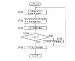
- FIG. 3 is a flowchart illustrating a processing procedure executed by the signal processing apparatus according to the present embodiment in the learning phase.
- the control unit 14 of the signal processing device executes the following processing in the initial state in which learning is not performed, so that the signal read unit 13 reads from the FRET network unit 12 and the calculation result by the FRET network unit 12 Learn the relationship.
- the control unit 14 executes the following processing to read the signal from the FRET network unit 12 and the calculation result by the FRET network unit 12. You may relearn the relationship with.
- the control unit 14 excites at least a part of the fluorescent particles 121, 121, ..., 121 constituting the FRET network unit 12 by controlling the signal input unit 11.
- the input signal to be calculated may be input to the control unit 14 through the input / output unit 16 or may be generated inside the control unit 14.
- the control unit 14 generates a modulation parameter according to the input signal to be calculated, and controls the wavelength and time-series light intensity of the excitation light to be irradiated according to the generated modulation parameter.
- the signal input unit 11 irradiates a predetermined irradiation region of the FRET network unit 12 with excitation light whose wavelength and time-series light intensity are controlled based on the modulation parameters generated by the control unit 14.
- the energy state of the fluorescent particles contained in the irradiation region changes from, for example, the ground state to the excited state.
- FRET is generated between the two fluorescent particles 121, 121 that satisfy the generation conditions.
- the FRET between the fluorescent particles 121 and 121 is generated one after another in the fluorescent particles 121, 121, ..., 121 constituting the nanostructure 120, and is transmitted to the entire nanostructure 120. That is, the energy states of the fluorescent particles 121, 121, ..., 121 are autonomously changed by FRET, and are changed to a state representing the calculation result.
- the signal reading unit 13 reads a signal from the FRET network unit 12 (step S102). This signal is read out after the timing when the energy state of the fluorescent particles 121, 121, ..., 121 changes to the state representing the calculation result (for example, after the timing when about 10 to 12 seconds have elapsed after irradiating the excitation light). You can do it at.
- the signal reading unit 13 can read a signal from the FRET network unit 12 by performing wavelength decomposition measurement / time decomposition measurement using a spectroscope.
- the signal read from the FRET network unit 12 is output to the control unit 14.
- the control unit 14 calculates a cost function set based on the signal read by the signal reading unit 13 and the teacher signal indicating the ideal output with respect to the input signal (step S103).
- the cost function L ( ⁇ k i ⁇ ) for example, represented by the following equation.
- y i (t, ⁇ ) represents a signal read by the signal reading unit 13 from the FRET network unit 12.
- f (x i ) represents a teacher signal indicating an ideal output with respect to the input signal x i .
- the calculation results corresponding to the signal y i (t, ⁇ ) is, F (y i (t, ⁇ ), ⁇ k i ⁇ ) can be written as.
- F is a function for converting the signal y i (t, ⁇ ) into an operation result.
- F may be a linear function or a non-linear function.
- cost function is not limited to the equation of Equation 1, and for example, the cost function represented by the following equation may be used.
- the control unit 14 the calculated value of the cost function L ( ⁇ k i ⁇ ) is equal to or less than the threshold value epsilon (step S104).
- the threshold value ⁇ is a threshold value for the cost function L ( ⁇ k i ⁇ ) to determine whether the convergence, suitable small value is set.
- the control unit 14 changes the parameters ⁇ k i ⁇ (step S105). For example, the control unit 14, holds the value of the cost function L calculated in step S103, the value L n of the current computed cost function L ( ⁇ k i ⁇ ) is the cost function L previously calculated ( ⁇ The parameter ⁇ x i ⁇ may be changed using the gradient method so that it is smaller than the value L n-1 of k i ⁇ ). After changing the parameter ⁇ x i ⁇ , the control unit 14 returns the process to step S101.
- controller 14 determines a parameter ⁇ k i ⁇ used in (step S106). Controller 14 stores the determined ⁇ k i ⁇ in the storage unit 15, the processing of this flowchart is terminated.
- FIG. 4 is a flowchart illustrating a processing procedure executed by the signal processing device according to the present embodiment in the operation phase.
- the control unit 14 of the signal processing device acquires the calculation result of the FRET network unit 12 from the signal read from the signal reading unit 13 by executing the following processing in the operation phase after the learning is completed.
- the control unit 14 controls the signal input unit 11 when the input signal to be calculated is input, so that the fluorescent particles 121, 121, ..., 121 constituting the FRET network unit 12 Excite at least a portion (step S201).
- the input signal to be calculated may be input to the control unit 14 through the input / output unit 16 or may be generated inside the control unit 14.
- the control unit 14 generates a modulation parameter according to the input signal to be calculated, and controls the wavelength and time-series light intensity of the excitation light to be irradiated according to the generated modulation parameter.
- the signal input unit 11 irradiates a predetermined irradiation region of the FRET network unit 12 with excitation light whose wavelength and time-series light intensity are controlled based on the modulation parameters generated by the control unit 14.
- the energy state of the fluorescent particles contained in the irradiation region changes from, for example, the ground state to the excited state.
- FRET is generated between the two fluorescent particles 121, 121 that satisfy the generation conditions.
- the FRET between the fluorescent particles 121 and 121 is generated one after another in the fluorescent particles 121, 121, ..., 121 constituting the nanostructure 120, and is transmitted to the entire nanostructure 120. That is, the energy states of the fluorescent particles 121, 121, ..., 121 are autonomously changed by FRET, and are changed to a state representing the calculation result.
- the signal reading unit 13 reads a signal from the FRET network unit 12 (step S202). This signal is read out after the timing when the energy state of the fluorescent particles 121, 121, ..., 121 changes to the state representing the calculation result (for example, after the timing when about 10 to 12 seconds have elapsed after irradiating the excitation light). You can do it at.
- the signal reading unit 13 can read a signal from the FRET network unit 12 by performing wavelength decomposition measurement / time decomposition measurement using a spectroscope.
- the signal read from the FRET network unit 12 is output to the control unit 14.
- control unit 14 derives the calculation result by the FRET network unit 12 based on the signal output from the signal reading unit 13 (step S203).
- the control unit 14 reads the parameters ⁇ k i ⁇ determined in the learning phase, the function F (y, ⁇ k i ⁇ ) described by the parameter ⁇ k i ⁇ to the signal y i (t, ⁇ ) signal
- the calculation result by the FRET network unit 12 is derived.
- the control unit 14 outputs the derived calculation result through the input / output unit 16 (step S204).
- the signal processing apparatus according to the present embodiment since the physical properties of the fluorescent particles 121 possessed by the FRET network unit 12 are directly used for the calculation, the signal processing apparatus according to the present embodiment is different from the conventional computing apparatus using the electric signal. In comparison, it is possible to realize miniaturization and low power consumption.
- FIG. 5 is a schematic diagram showing the configuration of the FRET network unit 12 in the second embodiment.
- the nanostructure 120 of the FRET network unit 12 in the second embodiment has a laminated structure in which the first layer 120A to the third layer 120C are laminated.
- the first layer 120A contains, for example, fluorescent particles 121A having a fluorescence wavelength of 540 nm
- the second layer 120B contains, for example, fluorescent particles 121B having a fluorescence wavelength of 580 nm
- the third layer 120C contains, for example, fluorescent particles having a fluorescence wavelength of 620 nm. Includes 121C.
- Each of these layers 120A to 120C is formed by spin-coating and then curing a polymer solvent containing fluorescent particles 121A to 121C on a cover glass.
- the fluorescent particles 121A are randomly arranged inside the first layer 120A.
- the fluorescent particles 121B are randomly arranged inside the second layer 120B
- the fluorescent particles 121C are randomly arranged inside the third layer 120C.
- the nanostructure 120 having a three-layer structure has been described as an example in FIG. 5, the nanostructure 120 may be a laminated body having two layers or four or more layers. Further, the nanostructure 120 may not have a layered structure and may have a structure in which fluorescent particles 121A, 121B, 121C are randomly arranged.
- the types of fluorescent particles randomly arranged are not limited to three, and may be two or four or more.
- the number of fluorescent particles 121A to 121C that contribute to energy transfer depends on the location where the excitation light is irradiated, even if the irradiation area of the excitation light is the same. different. For example, when the irradiation regions 111, 112, and 113 shown in FIG. 5 are irradiated with excitation light and fluorescence is observed in each of the observation regions 131, 132, and 133, the fluorescent particles 121A to 121C that contribute to energy transfer in each region. Since the number of particles is different, it is expected that the fluorescence intensity and fluorescence lifetime obtained as observation results will be different in each region.
- FIG. 6 is a diagram for explaining the verification result of verifying the diversity of fluorescence intensity.
- FIG. 6 shows the results of irradiating different regions of the nanostructure 120 shown in FIG. 5 with excitation light and observing the fluorescence intensity in each region.
- the irradiation regions 111, 112, and 113 were circular regions having a diameter of 16 ⁇ m.
- the observation areas 131, 132, and 133 corresponding to the irradiation areas 111, 112, and 113 are square areas having a side of 1 ⁇ m. The distance between the regions was 100 ⁇ m.
- a laser beam having a wavelength of 515 nm was used as the excitation light for irradiating the irradiation regions 111, 112, and 113.
- the diversity of fluorescence intensities was verified by performing wavelength decomposition measurement using a spectroscope.
- the wavelength dependence of the fluorescence intensity observed in each observation region 131, 132, 133 is as shown in the graph shown in the right column of FIG.
- the horizontal axis of each graph indicates the wavelength (nm), and the vertical axis indicates the fluorescence intensity (arbitrary scale).
- the fluorescence intensities observed in the observation regions 131, 132, and 133 have peaks near 540 nm, 580 nm, and 620 nm, indicating that energy transfer occurs between the fluorescent particles.
- the wavelength dependence of the fluorescence intensity differs depending on the observation regions 131, 132, and 133. It is presumed that the difference in fluorescence intensity is due to the difference in the densities of the fluorescent particles 121A, 121B, 121C in each region.
- the signal processing device gives the input signal a spatial modulation pattern, selectively excites the fluorescent particles 121A contained in the first layer 120A, and then reads a signal determined according to the spatial dynamics of the FRET network unit 12. Just put it out.
- FIG. 7 is a diagram for explaining the verification results for verifying the diversity of fluorescence lifetime.
- FIG. 7 shows the results of irradiating different regions of the nanostructure 120 shown in FIG. 5 with excitation light and observing the fluorescence lifetime in each region.
- the irradiation regions 111, 112, and 113 were circular regions having a diameter of 16 ⁇ m, as in the second embodiment.
- the observation areas 131, 132, and 133 corresponding to the irradiation areas 111, 112, and 113 are rectangular areas having a short side of 1 ⁇ m and a long side of 400 ⁇ m. The distance between the regions was 100 ⁇ m.
- a laser beam having a wavelength of 515 nm was used as the excitation light for irradiating the irradiation regions 111, 112, and 113.
- the diversity of fluorescence lifetime was verified by performing time-resolved measurement using a spectroscope.
- the temporal changes in fluorescence intensity observed in each observation area 131, 132, 133 are as shown in the graph shown in the right column of FIG.
- the horizontal axis of each graph shows time (ns), and the vertical axis shows fluorescence intensity (arbitrary scale).
- a curve fitted by the fitting function Aln ( ⁇ t / ⁇ 1) + Bln ( ⁇ t / ⁇ 2)
- ⁇ 1 and ⁇ 2 represent time constants, and their respective values are as shown in FIG. From the graph shown in FIG. 7, it can be seen that the fluorescence lifetimes observed in the observation regions 131, 132, and 133 differ depending on each region. It is presumed that the difference in fluorescence lifetime is due to the length of the energy transfer path caused by the difference in the distribution of the fluorescent particles 121A, 121B, 121C in each region.
- the signal processing device gives the input signal a spatial modulation pattern, selectively excites the fluorescent particles 121A contained in the first layer 120A, and then reads a signal determined according to the time dynamics of the FRET network unit 12. Just put it out.
- FIG. 8 is a diagram for explaining the verification results for verifying the diversity of fluorescence lifetime due to the difference in excitation intensity.
- FIG. 8 shows the results of irradiating the nanostructure 120 shown in FIG. 5 with excitation light having different excitation intensities and observing the fluorescence lifetime in each of them.
- the excitation light to irradiate the nanostructure 120 a laser beam having a wavelength of 510 nm and an intensity of 135 mW was used in the case of strong excitation, and a laser beam having a wavelength of 510 nm and an intensity of 20 mW was used in the case of weak excitation.
- the diversity of fluorescence lifetime was verified by performing time-resolved measurement using a spectroscope.
- the time change of the fluorescence intensity when the fluorescent particles 121A were excited under each excitation condition is as shown in the graph shown in FIG.
- the horizontal axis of each graph shows time (ns), and the vertical axis shows fluorescence intensity (arbitrary scale).
- a curve fitted by the fitting function Aln ( ⁇ t / ⁇ 1) + Bln ( ⁇ t / ⁇ 2) was used.
- the graph on the left side of FIG. 8 shows the fluorescence lifetime when strong excitation is performed, and the graph on the right side shows the fluorescence lifetime when weak excitation is performed.
- the five curves shown in each graph show the results of observation by changing the concentrations of the fluorescent particles 121A to 121C.
- the signal processing device may selectively excite the fluorescent particles 121A to 121C with the excitation intensity defined by the excitation conditions, and then read the signal determined according to the time dynamics of the FRET network unit 12.
Abstract
Provided are a signal processing device and signal processing method. This signal processing device comprises: a light energy network which contains a plurality of fluorescent particles and which is constituted in such a manner that energy movement paths via the plurality of fluorescent particles are determined autonomously and randomly; a signal input unit which excites at least some of the plurality of fluorescent particles, according to an input signal which should be input to a light energy network; a signal readout unit which, after some of the fluorescent particles are excited, reads out an optical signal from the light energy network; and an acquisition unit which acquires calculation results according to the light energy network, on the basis of a light signal read out by the signal readout unit.
Description
本発明は、信号処理装置及び信号処理方法に関する。
The present invention relates to a signal processing device and a signal processing method.
近年、蛍光粒子間の蛍光共鳴エネルギ移動(FRET:Fluorescence Resonance Energy Transfer)を利用した信号処理の実装により、微小サイズかつ低消費電力で計算を行う計算素子の開発が進められている(例えば、非特許文献1を参照)。
In recent years, the development of computational elements that perform calculations with a small size and low power consumption has been promoted by implementing signal processing using fluorescence resonance energy transfer (FRET) between fluorescent particles (for example, non-fluorescence). See Patent Document 1).
しかしながら、現在の微細加工技術では、大規模なFRET経路を設計通りに物理実装することは困難であるという問題点を有している。
However, with the current microfabrication technology, there is a problem that it is difficult to physically implement a large-scale FRET path as designed.
本発明は、大規模なFRET経路が物理実装された信号処理装置、及び信号処理方法を提供することを目的とする。
An object of the present invention is to provide a signal processing device in which a large-scale FRET path is physically mounted, and a signal processing method.
本発明の一態様に係る信号処理装置は、複数の蛍光粒子を含み、該複数の蛍光粒子を介したエネルギの移動経路が自律的かつランダムに定まるように構成された光エネルギネットワークと、前記光エネルギネットワークへ入力すべき入力信号に応じて、前記複数の蛍光粒子の少なくとも一部を励起させる信号入力部と、前記一部の蛍光粒子を励起させた後に、前記光エネルギネットワークから光信号を読み出す信号読出部と、該信号読出部により読み出した光信号に基づき、前記光エネルギネットワークによる演算結果を取得する取得部とを備える。
The signal processing apparatus according to one aspect of the present invention includes an optical energy network including a plurality of fluorescent particles and configured such that an energy transfer path through the plurality of fluorescent particles is autonomously and randomly determined, and the light. A signal input unit that excites at least a part of the plurality of fluorescent particles according to an input signal to be input to the energy network, and a signal input unit that excites some of the fluorescent particles, and then reads an optical signal from the photoenergy network. It includes a signal reading unit and an acquisition unit that acquires a calculation result by the optical energy network based on the optical signal read by the signal reading unit.
本発明の一態様に係る信号処理方法は、複数の蛍光粒子によるエネルギの移動経路が自律的かつランダムに定まるように構成された光エネルギネットワークへの入力信号の入力に応じて、前記複数の蛍光粒子の少なくとも一部を励起させ、前記一部の蛍光粒子を励起させた後に、前記光エネルギネットワークから光信号を読み出し、読み出した光信号に基づき、前記光エネルギネットワークによる演算結果を取得する。
In the signal processing method according to one aspect of the present invention, the plurality of fluorescences are received in response to the input of the input signal to the optical energy network configured so that the energy transfer path by the plurality of fluorescent particles is determined autonomously and randomly. After exciting at least a part of the particles and exciting the part of the fluorescent particles, the optical signal is read from the optical energy network, and the calculation result by the optical energy network is acquired based on the read optical signal.
上記一態様によれば、大規模なFRET経路による光エネルギネットワークを用いて信号処理を実行できる。
According to the above aspect, signal processing can be executed using an optical energy network based on a large-scale FRET path.
以下、本発明をその実施の形態を示す図面に基づいて具体的に説明する。
(実施の形態1)
図1は本実施の形態に係る信号処理装置の構成を示す模式図であり、図2はFRETネットワーク部12の構成を示す模式図である。本実施の形態に係る信号処理装置は、FRETにより信号が伝達する光エネルギネットワークを利用して演算を行う装置であり、信号入力部11、FRETネットワーク部12、信号読出部13、制御部14、記憶部15、及び入出力部16を備える。 Hereinafter, the present invention will be specifically described with reference to the drawings showing the embodiments thereof.
(Embodiment 1)
FIG. 1 is a schematic diagram showing the configuration of the signal processing device according to the present embodiment, and FIG. 2 is a schematic diagram showing the configuration of theFRET network unit 12. The signal processing device according to the present embodiment is a device that performs calculations using an optical energy network in which signals are transmitted by FRET, and is a signal input unit 11, FRET network unit 12, signal reading unit 13, control unit 14, It includes a storage unit 15 and an input / output unit 16.
(実施の形態1)
図1は本実施の形態に係る信号処理装置の構成を示す模式図であり、図2はFRETネットワーク部12の構成を示す模式図である。本実施の形態に係る信号処理装置は、FRETにより信号が伝達する光エネルギネットワークを利用して演算を行う装置であり、信号入力部11、FRETネットワーク部12、信号読出部13、制御部14、記憶部15、及び入出力部16を備える。 Hereinafter, the present invention will be specifically described with reference to the drawings showing the embodiments thereof.
(Embodiment 1)
FIG. 1 is a schematic diagram showing the configuration of the signal processing device according to the present embodiment, and FIG. 2 is a schematic diagram showing the configuration of the
FRETネットワーク部12は、複数の蛍光粒子121,121,…,121が固体中、液体中又はアモルファス中にランダムに配置されたナノ構造体120により構成される。ここで、蛍光粒子121は、蛍光分子であってもよく、量子ドットとして機能する蛍光材料であってもよい。また、ナノ構造体120は積層構造を有してもよい。ナノ構造体120に配置する蛍光粒子121の数は、隣接する蛍光粒子121,121間の距離が10nm以下となるように調整される。例えば、体積が1μm3 程度のナノ構造体120には106 個程度の蛍光粒子121が配置される。蛍光粒子121には、励起ピークが550nm、蛍光ピークが570nmのCy3、励起ピークが649nm、蛍光ピークが670nmのCy5等が用いられる。
The FRET network unit 12 is composed of nanostructures 120 in which a plurality of fluorescent particles 121, 121, ..., 121 are randomly arranged in a solid, a liquid, or an amorphous substance. Here, the fluorescent particle 121 may be a fluorescent molecule or a fluorescent material that functions as a quantum dot. Further, the nanostructure 120 may have a laminated structure. The number of fluorescent particles 121 arranged in the nanostructure 120 is adjusted so that the distance between adjacent fluorescent particles 121 and 121 is 10 nm or less. For example, volume is the nanostructures 120 of about 1 [mu] m 3 are disposed 106 about the fluorescent particles 121. As the fluorescent particles 121, Cy3 having an excitation peak of 550 nm and a fluorescence peak of 570 nm, Cy5 having an excitation peak of 649 nm, and a fluorescence peak of 670 nm are used.
蛍光粒子121はナノ構造体120においてランダムに配置されるので、任意の2つの蛍光粒子121,121間の距離は様々であるが、その距離がおよそ10nm以下である場合、FRETが発生し得る。なお、FRETの発生条件は、2つの蛍光粒子121,121間の距離だけでなく、ドナー側の発光スペクトルとアクセプタ側の吸収スペクトルとの重なりが大きいこと、2つの蛍光粒子121,121が適切な配向をとっていること、ドナー側の蛍光量子収率が大きく、かつ、アクセプタの吸収強度が大きいことが挙げられる。このようなナノ構造体120を用いることにより、FRETネットワーク部12では、蛍光粒子121,121間をエネルギが移動する経路は自律的かつランダムに定まる。すなわち、ナノ構造体120における蛍光粒子121,121,…,121は、FRETにより信号が伝達する光エネルギネットワークを構築する。
Since the fluorescent particles 121 are randomly arranged in the nanostructure 120, the distance between any two fluorescent particles 121, 121 varies, but if the distance is about 10 nm or less, FRET can occur. It should be noted that the FRET generation condition is that not only the distance between the two fluorescent particles 121 and 121 but also the overlap between the emission spectrum on the donor side and the absorption spectrum on the acceptor side is large, and the two fluorescent particles 121 and 121 are appropriate. It is oriented, the fluorescence quantum yield on the donor side is large, and the absorption intensity of the acceptor is large. By using such a nanostructure 120, in the FRET network unit 12, the path through which energy moves between the fluorescent particles 121 and 121 is determined autonomously and randomly. That is, the fluorescent particles 121, 121, ..., 121 in the nanostructure 120 construct an optical energy network through which signals are transmitted by FRET.
信号入力部11は、入力信号に応じて、蛍光粒子121,121,…,121の少なくとも一部を励起させる。入力信号は、信号処理装置において演算対象となる信号であり、制御部14の内部にて生成されてもよく、入出力部16を通じて外部から入力されてもよい。信号入力部11は、入力信号に応じて調整された変調パラメータに従って、ナノ構造体120へ照射すべき光の波長及び時系列光強度を制御し、波長及び時系列光強度を制御した光(以下、励起光という)をナノ構造体120の特定の照射領域へ照射する。変調方法は任意であり、予め設定したルールに従って変調されればよい。また、励起光を照射する照射領域は予め設定される。励起光が照射された場合、照射領域に含まれる蛍光粒子121,121,…,121のエネルギ状態は、例えば基底状態から励起状態へ遷移する。
The signal input unit 11 excites at least a part of the fluorescent particles 121, 121, ..., 121 according to the input signal. The input signal is a signal to be calculated in the signal processing device, may be generated inside the control unit 14, or may be input from the outside through the input / output unit 16. The signal input unit 11 controls the wavelength and time-series light intensity of the light to be irradiated to the nanostructure 120 according to the modulation parameters adjusted according to the input signal, and controls the wavelength and time-series light intensity (hereinafter referred to as light). , Excitation light) is applied to a specific irradiation region of the nanostructure 120. The modulation method is arbitrary, and it may be modulated according to a preset rule. Further, the irradiation region for irradiating the excitation light is set in advance. When the excitation light is irradiated, the energy states of the fluorescent particles 121, 121, ..., 121 included in the irradiation region change from, for example, the ground state to the excited state.
蛍光粒子121,121,…,121の一部が励起状態へ遷移した場合、上述した条件を満たす2つの蛍光粒子121,121間でFRETが発生する。すなわち、ドナー側の蛍光粒子121からアクセプタ側の蛍光粒子121へ励起エネルギが移動する。このような2つの蛍光粒子121,121間のFRETは、ナノ構造体120を構成する蛍光粒子121,121,…,121において次々に発生する。よって、信号入力部11によって励起光がナノ構造体120に照射された後、ナノ構造体120を構成する各蛍光粒子121,121,…,121のエネルギ状態は、発生条件を満たす他の蛍光粒子121からのFRETによって自律的に変化し、演算結果を表す状態へと変化する。
When a part of the fluorescent particles 121, 121, ..., 121 transitions to the excited state, FRET is generated between the two fluorescent particles 121, 121 that satisfy the above conditions. That is, the excitation energy is transferred from the fluorescent particles 121 on the donor side to the fluorescent particles 121 on the acceptor side. Such FRET between the two fluorescent particles 121 and 121 is generated one after another in the fluorescent particles 121, 121, ..., 121 constituting the nanostructure 120. Therefore, after the excitation light is irradiated to the nanostructure 120 by the signal input unit 11, the energy states of the fluorescent particles 121, 121, ..., 121 constituting the nanostructure 120 are other fluorescent particles satisfying the generation conditions. It changes autonomously by FRET from 121, and changes to a state that represents the calculation result.
信号読出部13は、信号入力部11から励起光を照射した後、各蛍光粒子121,121,…,121のエネルギ状態が演算結果を表す状態に変化したタイミング以降(例えば、励起光を照射してから10-12 秒程度が経過したタイミング以降)でFRETネットワーク部12から信号を読み出す。信号読出部13は、分光器を用いて波長分解計測/時間分解計測を行うことにより、FRETネットワーク部12から信号を読み出すことができる。FRETネットワーク部12から信号を読み出す手法は、公知の手法を用いることができる。また、信号読出部13が信号を読み出す読出領域は、ナノ構造体120の全領域を設定してもよく、ナノ構造体120の一部の領域を設定してもよい。信号読出部13によって読み出される信号は、読出領域に含まれる蛍光粒子121,121,…,121から得られる蛍光スペクトルの信号である。信号読出部13は、FRETネットワーク部12から読み出した信号を制御部14へ出力する。
After irradiating the excitation light from the signal input unit 11, the signal reading unit 13 irradiates the excitation light after the timing when the energy states of the fluorescent particles 121, 121, ..., 121 change to the states representing the calculation results (for example, irradiating the excitation light). The signal is read from the FRET network unit 12 (after the timing when about 10 to 12 seconds have passed since then). The signal reading unit 13 can read a signal from the FRET network unit 12 by performing wavelength decomposition measurement / time decomposition measurement using a spectroscope. As a method of reading a signal from the FRET network unit 12, a known method can be used. Further, the reading region for the signal reading unit 13 to read the signal may be set to the entire region of the nanostructure 120, or a part of the region of the nanostructure 120 may be set. The signal read by the signal reading unit 13 is a signal of the fluorescence spectrum obtained from the fluorescent particles 121, 121, ..., 121 included in the reading region. The signal reading unit 13 outputs the signal read from the FRET network unit 12 to the control unit 14.
制御部14は、CPU(Central Processing Unit)、ROM(Read Only Memory)、RAM(Random Access Memory)等を備える。制御部14のCPUは、ROM又は記憶部15に記憶された各種コンピュータプログラムを実行することにより、ハードウェア各部の動作の制御及び各種の演算を実行し、装置全体を本願の信号処理装置として機能させる。制御部14のRAMは、各種コンピュータプログラムの実行中に生成されるデータ等を一時的に記憶する。
The control unit 14 includes a CPU (Central Processing Unit), a ROM (Read Only Memory), a RAM (Random Access Memory), and the like. The CPU of the control unit 14 controls the operation of each hardware unit and executes various calculations by executing various computer programs stored in the ROM or the storage unit 15, and the entire device functions as the signal processing device of the present application. Let me. The RAM of the control unit 14 temporarily stores data and the like generated during execution of various computer programs.
制御部14が実行する演算は、信号読出部13がFRETネットワーク部12から読み出す信号と、FRETネットワーク部12による演算結果との関係を学習する演算、および、学習演算の結果を利用して、FRETネットワーク部12が読み出した信号から演算結果を導出する演算を含む。これらの演算については、後に詳述することとする。
The calculation executed by the control unit 14 is a calculation for learning the relationship between the signal read by the signal reading unit 13 from the FRET network unit 12 and the calculation result by the FRET network unit 12, and the calculation using the result of the learning calculation is used for FRET. It includes an operation of deriving an operation result from a signal read by the network unit 12. These operations will be described in detail later.
なお、制御部14は、上記の構成に限定されるものではなく、1又は複数のCPU、マルチコアCPU、GPU(Graphics Processing Unit)、マイコン等を含む任意の処理回路であればよい。また、制御部14は、日時情報を出力するクロック、計測開始指示を与えてから計測終了指示を与えるまでの経過時間を計測するタイマ、数をカウントするカウンタ等の機能を備えていてもよい。
The control unit 14 is not limited to the above configuration, and may be any processing circuit including one or a plurality of CPUs, a multi-core CPU, a GPU (Graphics Processing Unit), a microcomputer, and the like. Further, the control unit 14 may have functions such as a clock for outputting date and time information, a timer for measuring the elapsed time from giving the measurement start instruction to giving the measurement end instruction, and a counter for counting the number.
記憶部15は、メモリやHDD(Hard Disk Drive)などを用いた記憶装置を備える。記憶部15には、制御部14によって実行される各種コンピュータプログラム、コンピュータプログラムの実行に必要なデータ、制御部14による演算結果等が記憶される。記憶部15に記憶されるコンピュータプログラムは、信号読出部13がFRETネットワーク部12から読み出す信号と入力信号に対する出力として取得すべき演算結果との関係を学習するための学習プログラム、及び、学習結果に基づき、FRETネットワーク部12から信号読出部13が読み出した信号を演算結果に変換するための計算プログラム等を含む。
The storage unit 15 includes a storage device that uses a memory, an HDD (Hard Disk Drive), or the like. The storage unit 15 stores various computer programs executed by the control unit 14, data necessary for executing the computer programs, calculation results by the control unit 14, and the like. The computer program stored in the storage unit 15 is a learning program for learning the relationship between the signal read from the FRET network unit 12 by the signal reading unit 13 and the calculation result to be acquired as an output for the input signal, and the learning result. Based on this, it includes a calculation program for converting the signal read by the signal reading unit 13 from the FRET network unit 12 into a calculation result.
なお、記憶部15に記憶されるコンピュータプログラムは、当該コンピュータプログラムを読み取り可能に記録した非一時的な記録媒体により提供されてもよい。記録媒体は、例えば、CD-ROM、USBメモリ、SD(Secure Digital)カード、マイクロSDカード、コンパクトフラッシュ(登録商標)などの可搬型メモリである。この場合、制御部14は、不図示の読取装置を用いて記録媒体からコンピュータプログラムを読み取り、読み取ったコンピュータプログラムを記憶部15にインストールすることが可能である。また、記憶部15に記憶されるコンピュータプログラムは通信により提供されてもよい。この場合、制御部14は、不図示の外部サーバと通信を行うことによってコンピュータプログラムを取得し、取得したコンピュータプログラムを記憶部15にインストールすることができる。
The computer program stored in the storage unit 15 may be provided by a non-temporary recording medium in which the computer program is readablely recorded. The recording medium is, for example, a portable memory such as a CD-ROM, a USB memory, an SD (Secure Digital) card, a micro SD card, or a compact flash (registered trademark). In this case, the control unit 14 can read the computer program from the recording medium using a reading device (not shown), and install the read computer program in the storage unit 15. Further, the computer program stored in the storage unit 15 may be provided by communication. In this case, the control unit 14 can acquire a computer program by communicating with an external server (not shown), and can install the acquired computer program in the storage unit 15.
入出力部16は、各種情報を入出力するためのインタフェースを備える。入出力部16は、キーボード、マウス等の入力デバイスを接続するインタフェースを備え、接続された入力デバイスを通じてユーザの指示を受け付けてもよい。また、入出力部16は、外部コンピュータを接続するインタフェースを備え、接続された外部コンピュータから出力される信号が入力されてもよい。更に、入出力部16は、液晶ディスプレイ、有機EL(Electro-Luminescence)ディスプレイ等の出力デバイスを接続するインタフェースを備え、制御部14による演算結果等を出力デバイスへ出力してもよい。
The input / output unit 16 includes an interface for inputting / outputting various information. The input / output unit 16 includes an interface for connecting an input device such as a keyboard and a mouse, and may receive a user's instruction through the connected input device. Further, the input / output unit 16 includes an interface for connecting an external computer, and a signal output from the connected external computer may be input. Further, the input / output unit 16 may include an interface for connecting an output device such as a liquid crystal display or an organic EL (Electro-Luminescence) display, and output the calculation result or the like by the control unit 14 to the output device.
以下、本実施の形態に係る信号処理装置の動作について説明する。
図3は学習フェーズにおいて本実施の形態に係る信号処理装置が実行する処理の手順を説明するフローチャートである。信号処理装置の制御部14は、学習が行われていない初期状態において、以下の処理を実行することにより、信号読出部13がFRETネットワーク部12から読み出す信号と、FRETネットワーク部12による演算結果との関係を学習する。また、入出力部16を通じてユーザの指示を受付けた場合、制御部14は、以下の処理を実行することにより、信号読出部13がFRETネットワーク部12から読み出す信号と、FRETネットワーク部12による演算結果との関係を再学習してもよい。 Hereinafter, the operation of the signal processing device according to the present embodiment will be described.
FIG. 3 is a flowchart illustrating a processing procedure executed by the signal processing apparatus according to the present embodiment in the learning phase. Thecontrol unit 14 of the signal processing device executes the following processing in the initial state in which learning is not performed, so that the signal read unit 13 reads from the FRET network unit 12 and the calculation result by the FRET network unit 12 Learn the relationship. When the user's instruction is received through the input / output unit 16, the control unit 14 executes the following processing to read the signal from the FRET network unit 12 and the calculation result by the FRET network unit 12. You may relearn the relationship with.
図3は学習フェーズにおいて本実施の形態に係る信号処理装置が実行する処理の手順を説明するフローチャートである。信号処理装置の制御部14は、学習が行われていない初期状態において、以下の処理を実行することにより、信号読出部13がFRETネットワーク部12から読み出す信号と、FRETネットワーク部12による演算結果との関係を学習する。また、入出力部16を通じてユーザの指示を受付けた場合、制御部14は、以下の処理を実行することにより、信号読出部13がFRETネットワーク部12から読み出す信号と、FRETネットワーク部12による演算結果との関係を再学習してもよい。 Hereinafter, the operation of the signal processing device according to the present embodiment will be described.
FIG. 3 is a flowchart illustrating a processing procedure executed by the signal processing apparatus according to the present embodiment in the learning phase. The
制御部14は、演算対象となる入力信号が入力された場合、信号入力部11を制御することによって、FRETネットワーク部12を構成する蛍光粒子121,121,…,121の少なくとも一部を励起させる(ステップS101)。演算対象となる入力信号は、入出力部16を通じて制御部14に入力されてもよく、制御部14の内部にて生成されてもよい。制御部14は、演算対象の入力信号に応じて変調パラメータを生成し、生成した変調パラメータに従って照射すべき励起光の波長及び時系列光強度を制御する。信号入力部11は、制御部14によって生成される変調パラメータに基づき波長及び時系列光強度が制御された励起光をFRETネットワーク部12の予め定められた照射領域へ照射する。
When the input signal to be calculated is input, the control unit 14 excites at least a part of the fluorescent particles 121, 121, ..., 121 constituting the FRET network unit 12 by controlling the signal input unit 11. (Step S101). The input signal to be calculated may be input to the control unit 14 through the input / output unit 16 or may be generated inside the control unit 14. The control unit 14 generates a modulation parameter according to the input signal to be calculated, and controls the wavelength and time-series light intensity of the excitation light to be irradiated according to the generated modulation parameter. The signal input unit 11 irradiates a predetermined irradiation region of the FRET network unit 12 with excitation light whose wavelength and time-series light intensity are controlled based on the modulation parameters generated by the control unit 14.
励起光の照射によって、照射領域に含まれる蛍光粒子のエネルギ状態は、例えば基底状態から励起状態へ遷移する。蛍光粒子121,121,…,121の一部が励起状態へ遷移した場合、発生条件を満たす2つの蛍光粒子121,121間でFRETが発生する。蛍光粒子121,121間のFRETは、ナノ構造体120を構成する蛍光粒子121,121,…,121において次々に発生し、ナノ構造体120の全体に伝わる。すなわち、蛍光粒子121,121,…,121のエネルギ状態はFRETによって自律的に変化し、演算結果を表す状態へと変化する。
By irradiation with excitation light, the energy state of the fluorescent particles contained in the irradiation region changes from, for example, the ground state to the excited state. When a part of the fluorescent particles 121, 121, ..., 121 transitions to the excited state, FRET is generated between the two fluorescent particles 121, 121 that satisfy the generation conditions. The FRET between the fluorescent particles 121 and 121 is generated one after another in the fluorescent particles 121, 121, ..., 121 constituting the nanostructure 120, and is transmitted to the entire nanostructure 120. That is, the energy states of the fluorescent particles 121, 121, ..., 121 are autonomously changed by FRET, and are changed to a state representing the calculation result.
次いで、信号読出部13は、FRETネットワーク部12から信号の読み出しを行う(ステップS102)。この信号の読み出しは、蛍光粒子121,121,…,121のエネルギ状態が演算結果を表す状態に変化したタイミング以降(例えば、励起光を照射してから10-12 秒程度が経過したタイミング以降)にて行えばよい。信号読出部13は、分光器を用いて波長分解計測/時間分解計測を行うことにより、FRETネットワーク部12から信号を読み出すことができる。FRETネットワーク部12から読み出された信号は、制御部14へ出力される。
Next, the signal reading unit 13 reads a signal from the FRET network unit 12 (step S102). This signal is read out after the timing when the energy state of the fluorescent particles 121, 121, ..., 121 changes to the state representing the calculation result (for example, after the timing when about 10 to 12 seconds have elapsed after irradiating the excitation light). You can do it at. The signal reading unit 13 can read a signal from the FRET network unit 12 by performing wavelength decomposition measurement / time decomposition measurement using a spectroscope. The signal read from the FRET network unit 12 is output to the control unit 14.
次いで、制御部14は、信号読出部13によって読み出される信号と、入力信号に対する理想的な出力を示す教師信号とに基づき設定されるコスト関数を算出する(ステップS103)。コスト関数L({ki })は、例えば、次式により表される。
Next, the control unit 14 calculates a cost function set based on the signal read by the signal reading unit 13 and the teacher signal indicating the ideal output with respect to the input signal (step S103). The cost function L ({k i}), for example, represented by the following equation.

ここで、xi (i=1,2,3,…)は入力信号、yi (t,λ)は信号読出部13がFRETネットワーク部12から読み出した信号を表している。f(xi )は、入力信号xi に対して理想的な出力を示す教師信号を表す。また、信号yi (t,λ)に対応する演算結果は、F(yi (t,λ),{ki })のように記述することができる。ここで、F(…)は信号yi (t,λ)を演算結果に変換するための関数である。F(…)は、線形関数であってもよく、非線形関数であってもよい。{ki }は、関数F(…)を用いて、信号yi (t,λ)を演算結果に変換する際に用いられるパラメータである。パラメータ{ki }は、学習によって調整される。
Here, x i (i = 1, 2, 3, ...) Represents an input signal, and y i (t, λ) represents a signal read by the signal reading unit 13 from the FRET network unit 12. f (x i ) represents a teacher signal indicating an ideal output with respect to the input signal x i . The calculation results corresponding to the signal y i (t, λ) is, F (y i (t, λ), {k i}) can be written as. Here, F (...) is a function for converting the signal y i (t, λ) into an operation result. F (...) may be a linear function or a non-linear function. {K i}, using function F (...), is a parameter used to convert the signals y i (t, λ) to the result. Parameter {k i} are adjusted by learning.
なお、コスト関数は数1の式に限定されるものではなく、例えば、次式で表されるコスト関数を用いてもよい。
Note that the cost function is not limited to the equation of Equation 1, and for example, the cost function represented by the following equation may be used.

次いで、制御部14は、算出したコスト関数L({ki })の値が閾値ε以下であるか否かを判断する(ステップS104)。ここで、閾値εは、コスト関数L({ki })が収束したか否かを判定するための閾値であり、適宜の微小な値が設定される。
Then, the control unit 14, the calculated value of the cost function L ({k i}) is equal to or less than the threshold value epsilon (step S104). Here, the threshold value ε is a threshold value for the cost function L ({k i}) to determine whether the convergence, suitable small value is set.
算出したコスト関数Lの値が閾値ε以下でないと判断した場合(S104:NO)、制御部14は、パラメータ{ki }を変更する(ステップS105)。例えば、制御部14は、ステップS103で算出されるコスト関数Lの値を保持しておき、今回算出したコスト関数L({ki })の値Ln が、前回算出したコスト関数L({ki })の値Ln-1 よりも小さくなるように、勾配法を用いてパラメータ{xi }を変更してもよい。パラメータ{xi }を変更した後、制御部14は、処理をステップS101へ戻す。
If the calculated value of the cost function L is determined to not less than the threshold value ε (S104: NO), the control unit 14 changes the parameters {k i} (step S105). For example, the control unit 14, holds the value of the cost function L calculated in step S103, the value L n of the current computed cost function L ({k i}) is the cost function L previously calculated ({ The parameter {x i } may be changed using the gradient method so that it is smaller than the value L n-1 of k i }). After changing the parameter {x i }, the control unit 14 returns the process to step S101.
一方、算出したコスト関数L({ki })の値が閾値ε以下であると判断した場合(S104:YES)、制御部14は、そのときのパラメータ{ki }の値を、運用フェーズで用いるパラメータ{ki }として決定する(ステップS106)。制御部14は、決定した{ki }を記憶部15に記憶させ、本フローチャートによる処理を終了する。
On the other hand, if the calculated value of the cost function L ({k i}) is equal to or less than the threshold value ε (S104: YES), the control unit 14, the value of the parameter {k i} at that time, operation phase determining a parameter {k i} used in (step S106). Controller 14 stores the determined {k i} in the storage unit 15, the processing of this flowchart is terminated.
図4は運用フェーズにおいて本実施の形態に係る信号処理装置が実行する処理の手順を説明するフローチャートである。信号処理装置の制御部14は、学習が完了した後の運用フェーズにおいて、以下の処理を実行することにより、信号読出部13から読み出した信号からFRETネットワーク部12の演算結果を取得する。
FIG. 4 is a flowchart illustrating a processing procedure executed by the signal processing device according to the present embodiment in the operation phase. The control unit 14 of the signal processing device acquires the calculation result of the FRET network unit 12 from the signal read from the signal reading unit 13 by executing the following processing in the operation phase after the learning is completed.
制御部14は、学習フェーズと同様に、演算対象となる入力信号が入力された場合、信号入力部11を制御することによって、FRETネットワーク部12を構成する蛍光粒子121,121,…,121の少なくとも一部を励起させる(ステップS201)。演算対象となる入力信号は、入出力部16を通じて制御部14に入力されてもよく、制御部14の内部にて生成されてもよい。制御部14は、演算対象の入力信号に応じて変調パラメータを生成し、生成した変調パラメータに従って照射すべき励起光の波長及び時系列光強度を制御する。信号入力部11は、制御部14によって生成される変調パラメータに基づき波長及び時系列光強度が制御された励起光をFRETネットワーク部12の予め定められた照射領域へ照射する。
Similar to the learning phase, the control unit 14 controls the signal input unit 11 when the input signal to be calculated is input, so that the fluorescent particles 121, 121, ..., 121 constituting the FRET network unit 12 Excite at least a portion (step S201). The input signal to be calculated may be input to the control unit 14 through the input / output unit 16 or may be generated inside the control unit 14. The control unit 14 generates a modulation parameter according to the input signal to be calculated, and controls the wavelength and time-series light intensity of the excitation light to be irradiated according to the generated modulation parameter. The signal input unit 11 irradiates a predetermined irradiation region of the FRET network unit 12 with excitation light whose wavelength and time-series light intensity are controlled based on the modulation parameters generated by the control unit 14.
励起光の照射によって、照射領域に含まれる蛍光粒子のエネルギ状態は、例えば基底状態から励起状態へ遷移する。蛍光粒子121,121,…,121の一部が励起状態へ遷移した場合、発生条件を満たす2つの蛍光粒子121,121間でFRETが発生する。蛍光粒子121,121間のFRETは、ナノ構造体120を構成する蛍光粒子121,121,…,121において次々に発生し、ナノ構造体120の全体に伝わる。すなわち、蛍光粒子121,121,…,121のエネルギ状態はFRETによって自律的に変化し、演算結果を表す状態へと変化する。
By irradiation with excitation light, the energy state of the fluorescent particles contained in the irradiation region changes from, for example, the ground state to the excited state. When a part of the fluorescent particles 121, 121, ..., 121 transitions to the excited state, FRET is generated between the two fluorescent particles 121, 121 that satisfy the generation conditions. The FRET between the fluorescent particles 121 and 121 is generated one after another in the fluorescent particles 121, 121, ..., 121 constituting the nanostructure 120, and is transmitted to the entire nanostructure 120. That is, the energy states of the fluorescent particles 121, 121, ..., 121 are autonomously changed by FRET, and are changed to a state representing the calculation result.
次いで、信号読出部13は、FRETネットワーク部12から信号の読み出しを行う(ステップS202)。この信号の読み出しは、蛍光粒子121,121,…,121のエネルギ状態が演算結果を表す状態に変化したタイミング以降(例えば、励起光を照射してから10-12 秒程度が経過したタイミング以降)にて行えばよい。信号読出部13は、分光器を用いて波長分解計測/時間分解計測を行うことにより、FRETネットワーク部12から信号を読み出すことができる。FRETネットワーク部12から読み出された信号は、制御部14へ出力される。
Next, the signal reading unit 13 reads a signal from the FRET network unit 12 (step S202). This signal is read out after the timing when the energy state of the fluorescent particles 121, 121, ..., 121 changes to the state representing the calculation result (for example, after the timing when about 10 to 12 seconds have elapsed after irradiating the excitation light). You can do it at. The signal reading unit 13 can read a signal from the FRET network unit 12 by performing wavelength decomposition measurement / time decomposition measurement using a spectroscope. The signal read from the FRET network unit 12 is output to the control unit 14.
次いで、制御部14は、信号読出部13から出力される信号に基づき、FRETネットワーク部12による演算結果を導出する(ステップS203)。このとき、制御部14は、学習フェーズにおいて決定したパラメータ{ki }を読み出し、パラメータ{ki }により記述される関数F(y,{ki })へ信号yi(t,λ)信号入力することによって、FRETネットワーク部12による演算結果を導出する。制御部14は、入出力部16を通じて、導出した演算結果を出力する(ステップS204)。
Next, the control unit 14 derives the calculation result by the FRET network unit 12 based on the signal output from the signal reading unit 13 (step S203). At this time, the control unit 14 reads the parameters {k i} determined in the learning phase, the function F (y, {k i} ) described by the parameter {k i} to the signal y i (t, λ) signal By inputting, the calculation result by the FRET network unit 12 is derived. The control unit 14 outputs the derived calculation result through the input / output unit 16 (step S204).
以上のように、本実施の形態に係る信号処理装置では、FRETネットワーク部12が有する蛍光粒子121の物理的性質を直接的に演算に用いているので、電気信号を用いた従来の計算装置と比較し、小型化及び低消費電力化を実現することができる。
As described above, in the signal processing apparatus according to the present embodiment, since the physical properties of the fluorescent particles 121 possessed by the FRET network unit 12 are directly used for the calculation, the signal processing apparatus according to the present embodiment is different from the conventional computing apparatus using the electric signal. In comparison, it is possible to realize miniaturization and low power consumption.
(実施の形態2)
実施の形態2では、FRETネットワーク部12の空間ダイナミクスを利用した信号処理装置について説明する。 (Embodiment 2)
In the second embodiment, a signal processing device using the spatial dynamics of theFRET network unit 12 will be described.
実施の形態2では、FRETネットワーク部12の空間ダイナミクスを利用した信号処理装置について説明する。 (Embodiment 2)
In the second embodiment, a signal processing device using the spatial dynamics of the
図5は実施の形態2におけるFRETネットワーク部12の構成を示す模式図である。実施の形態2におけるFRETネットワーク部12のナノ構造体120は、第1層120A~第3層120Cを積層した積層構造を有する。第1層120Aは、例えば蛍光波長が540nmの蛍光粒子121Aを含み、第2層120Bは、例えば蛍光波長が580nmの蛍光粒子121Bを含み、第3層120Cは、例えば蛍光波長が620nmの蛍光粒子121Cを含む。これらの各層120A~120Cは、蛍光粒子121A~121Cを含有したポリマー溶剤をカバーガラス上でスピンコート後に硬化することによって形成される。蛍光粒子121Aは、第1層120Aの内部にてランダムに配置される。同様に、蛍光粒子121Bは、第2層120Bの内部にてランダムに配置され、蛍光粒子121Cは、第3層120Cの内部にてランダムに配置される。なお、図5では3層構造のナノ構造体120を例に挙げて説明したが、ナノ構造体120は、2層又は4層以上の積層体であってもよい。また、ナノ構造体120は、層構造を持たず、蛍光粒子121A,121B,121Cがランダムに配置された構造であってもよい。ランダムに配置される蛍光粒子の種類は3種類に限らず、2種類又は4種類以上であってもよい。
FIG. 5 is a schematic diagram showing the configuration of the FRET network unit 12 in the second embodiment. The nanostructure 120 of the FRET network unit 12 in the second embodiment has a laminated structure in which the first layer 120A to the third layer 120C are laminated. The first layer 120A contains, for example, fluorescent particles 121A having a fluorescence wavelength of 540 nm, the second layer 120B contains, for example, fluorescent particles 121B having a fluorescence wavelength of 580 nm, and the third layer 120C contains, for example, fluorescent particles having a fluorescence wavelength of 620 nm. Includes 121C. Each of these layers 120A to 120C is formed by spin-coating and then curing a polymer solvent containing fluorescent particles 121A to 121C on a cover glass. The fluorescent particles 121A are randomly arranged inside the first layer 120A. Similarly, the fluorescent particles 121B are randomly arranged inside the second layer 120B, and the fluorescent particles 121C are randomly arranged inside the third layer 120C. Although the nanostructure 120 having a three-layer structure has been described as an example in FIG. 5, the nanostructure 120 may be a laminated body having two layers or four or more layers. Further, the nanostructure 120 may not have a layered structure and may have a structure in which fluorescent particles 121A, 121B, 121C are randomly arranged. The types of fluorescent particles randomly arranged are not limited to three, and may be two or four or more.
図5に示すナノ構造体120において、蛍光波長が540nmの蛍光粒子121Aから蛍光波長580nmの蛍光粒子121Bへのエネルギ移動は許容され、その逆方向への移動は禁止される。同様に、蛍光波長が580nmの蛍光粒子121Bから蛍光波長620nmの蛍光粒子121Cへのエネルギ移動は許容され、その逆方向への移動は禁止される。したがって、第1層120Aの側からナノ構造体120に励起光を照射し、第1層120A内の蛍光粒子121Aを励起した場合、そのエネルギ状態は、第1層120A内の蛍光粒子121A、第2層120B内の蛍光粒子121B、第3層120C内の蛍光粒子121Cの順に順次伝わる。蛍光粒子121Cが発する蛍光は、ナノ構造体120の第3層120Cの側から観測可能である。
In the nanostructure 120 shown in FIG. 5, energy transfer from fluorescent particles 121A having a fluorescence wavelength of 540 nm to fluorescent particles 121B having a fluorescence wavelength of 580 nm is permitted, and transfer in the opposite direction is prohibited. Similarly, energy transfer from fluorescent particles 121B having a fluorescence wavelength of 580 nm to fluorescent particles 121C having a fluorescence wavelength of 620 nm is permitted, and transfer in the opposite direction is prohibited. Therefore, when the nanostructure 120 is irradiated with excitation light from the side of the first layer 120A to excite the fluorescent particles 121A in the first layer 120A, the energy state thereof is the fluorescent particles 121A and the first in the first layer 120A. The fluorescent particles 121B in the second layer 120B and the fluorescent particles 121C in the third layer 120C are transmitted in this order. The fluorescence emitted by the fluorescent particles 121C can be observed from the side of the third layer 120C of the nanostructure 120.
蛍光粒子121A~121Cは、各層内においてランダムに配置されるので、励起光の照射面積が同じであっても、エネルギ移動に寄与する蛍光粒子121A~121Cの数は、励起光を照射する場所によって異なる。例えば、図5に示す照射領域111,112,113にそれぞれ励起光を照射し、観測領域131,132,133のそれぞれにおいて蛍光を観測した場合、各領域においてエネルギ移動に寄与する蛍光粒子121A~121Cの数は異なるので、観測結果として得られる蛍光強度及び蛍光寿命は各領域において異なることが予想される。
Since the fluorescent particles 121A to 121C are randomly arranged in each layer, the number of fluorescent particles 121A to 121C that contribute to energy transfer depends on the location where the excitation light is irradiated, even if the irradiation area of the excitation light is the same. different. For example, when the irradiation regions 111, 112, and 113 shown in FIG. 5 are irradiated with excitation light and fluorescence is observed in each of the observation regions 131, 132, and 133, the fluorescent particles 121A to 121C that contribute to energy transfer in each region. Since the number of particles is different, it is expected that the fluorescence intensity and fluorescence lifetime obtained as observation results will be different in each region.
図6は蛍光強度の多様性を検証した検証結果を説明する図である。図6は、図5に示すナノ構造体120の異なる領域に励起光を照射し、それぞれにおいて蛍光強度を観測した結果を示している。照射領域111,112,113は、直径16μmの円形領域とした。各照射領域111,112,113に対応する観測領域131,132,133は、一辺が1μmの正方形領域とした。各領域間の間隔は、100μmとした。照射領域111,112,113に照射する励起光には、515nmの波長を有するレーザ光を用いた。本実施の形態では、分光器を用いて波長分解計測を行うことにより、蛍光強度の多様性を検証した。
FIG. 6 is a diagram for explaining the verification result of verifying the diversity of fluorescence intensity. FIG. 6 shows the results of irradiating different regions of the nanostructure 120 shown in FIG. 5 with excitation light and observing the fluorescence intensity in each region. The irradiation regions 111, 112, and 113 were circular regions having a diameter of 16 μm. The observation areas 131, 132, and 133 corresponding to the irradiation areas 111, 112, and 113 are square areas having a side of 1 μm. The distance between the regions was 100 μm. A laser beam having a wavelength of 515 nm was used as the excitation light for irradiating the irradiation regions 111, 112, and 113. In this embodiment, the diversity of fluorescence intensities was verified by performing wavelength decomposition measurement using a spectroscope.
各観測領域131,132,133において観測される蛍光強度の波長依存性は、図6の右欄に示すグラフのようになった。各グラフの横軸は波長(nm)を示し、縦軸は蛍光強度(任意目盛り)を示している。各観測領域131,132,133において観測される蛍光強度は、540nm,580nm,620nm付近にピークを有しており、蛍光粒子間でエネルギ移動が生じていることが分かる。また、図6に示すグラフから、蛍光強度の波長依存性は観測領域131,132,133に応じて相違することが分かる。蛍光強度の相違は、各領域内における蛍光粒子121A,121B,121Cの密度の相違に由来するものであると推察される。
The wavelength dependence of the fluorescence intensity observed in each observation region 131, 132, 133 is as shown in the graph shown in the right column of FIG. The horizontal axis of each graph indicates the wavelength (nm), and the vertical axis indicates the fluorescence intensity (arbitrary scale). The fluorescence intensities observed in the observation regions 131, 132, and 133 have peaks near 540 nm, 580 nm, and 620 nm, indicating that energy transfer occurs between the fluorescent particles. Further, from the graph shown in FIG. 6, it can be seen that the wavelength dependence of the fluorescence intensity differs depending on the observation regions 131, 132, and 133. It is presumed that the difference in fluorescence intensity is due to the difference in the densities of the fluorescent particles 121A, 121B, 121C in each region.
このように、観測領域131,132,133に応じて多彩な蛍光スペクトルが得られるので、上述したナノ構造体120をリザーバに応用可能であることが示唆される。すなわち、信号処理装置は、入力信号に空間変調パターンを持たせ、第1層120Aに含まれる蛍光粒子121Aを選択的に励起させた後に、FRETネットワーク部12の空間ダイナミクスに応じて定まる信号を読み出せばよい。
As described above, various fluorescence spectra can be obtained according to the observation regions 131, 132, and 133, suggesting that the above-mentioned nanostructure 120 can be applied to the reservoir. That is, the signal processing device gives the input signal a spatial modulation pattern, selectively excites the fluorescent particles 121A contained in the first layer 120A, and then reads a signal determined according to the spatial dynamics of the FRET network unit 12. Just put it out.
(実施の形態3)
実施の形態3では、FRETネットワーク部12の時間ダイナミクスを利用した信号処理装置について説明する。 (Embodiment 3)
In the third embodiment, a signal processing device using the time dynamics of theFRET network unit 12 will be described.
実施の形態3では、FRETネットワーク部12の時間ダイナミクスを利用した信号処理装置について説明する。 (Embodiment 3)
In the third embodiment, a signal processing device using the time dynamics of the
図7は蛍光寿命の多様性を検証した検証結果を説明する図である。図7は、図5に示すナノ構造体120の異なる領域に励起光を照射し、それぞれにおいて蛍光寿命を観測した結果を示している。照射領域111,112,113は、実施の形態2と同様に、直径16μmの円形領域とした。各照射領域111,112,113に対応する観測領域131,132,133は、短辺が1μm、長辺が400μmの矩形領域とした。各領域間の間隔は、100μmとした。照射領域111,112,113に照射する励起光には、515nmの波長を有するレーザ光を用いた。本実施の形態では、分光器を用いて時間分解計測を行うことにより、蛍光寿命の多様性を検証した。
FIG. 7 is a diagram for explaining the verification results for verifying the diversity of fluorescence lifetime. FIG. 7 shows the results of irradiating different regions of the nanostructure 120 shown in FIG. 5 with excitation light and observing the fluorescence lifetime in each region. The irradiation regions 111, 112, and 113 were circular regions having a diameter of 16 μm, as in the second embodiment. The observation areas 131, 132, and 133 corresponding to the irradiation areas 111, 112, and 113 are rectangular areas having a short side of 1 μm and a long side of 400 μm. The distance between the regions was 100 μm. A laser beam having a wavelength of 515 nm was used as the excitation light for irradiating the irradiation regions 111, 112, and 113. In the present embodiment, the diversity of fluorescence lifetime was verified by performing time-resolved measurement using a spectroscope.
各観測領域131,132,133において観測される蛍光強度の時間変化は、図7の右欄に示すグラフのようになった。各グラフの横軸は時間(ns)、縦軸は蛍光強度(任意目盛り)を示している。蛍光寿命を示す曲線には、フィッティング関数(Aln(-t/τ1)+Bln(-t/τ2))でフィッティングした曲線を用いた。ここで、τ1,τ2は時定数を表し、それぞれの値は図7に示す通りとなった。図7に示すグラフから、各観測領域131,132,133において観測される蛍光寿命は、各領域に応じて相違することが分かる。蛍光寿命の相違は、各領域内における蛍光粒子121A,121B,121Cの分布の相違に起因したエネルギ伝達経路の長短に由来するものであると推察される。
The temporal changes in fluorescence intensity observed in each observation area 131, 132, 133 are as shown in the graph shown in the right column of FIG. The horizontal axis of each graph shows time (ns), and the vertical axis shows fluorescence intensity (arbitrary scale). As the curve showing the fluorescence lifetime, a curve fitted by the fitting function (Aln (−t / τ1) + Bln (−t / τ2)) was used. Here, τ1 and τ2 represent time constants, and their respective values are as shown in FIG. From the graph shown in FIG. 7, it can be seen that the fluorescence lifetimes observed in the observation regions 131, 132, and 133 differ depending on each region. It is presumed that the difference in fluorescence lifetime is due to the length of the energy transfer path caused by the difference in the distribution of the fluorescent particles 121A, 121B, 121C in each region.
このように、観測領域131,132,133に応じて多彩な蛍光スペクトルが得られるので、上述したナノ構造体120をリザーバに応用可能であることが示唆される。すなわち、信号処理装置は、入力信号に空間変調パターンを持たせ、第1層120Aに含まれる蛍光粒子121Aを選択的に励起させた後に、FRETネットワーク部12の時間ダイナミクスに応じて定まる信号を読み出せばよい。
As described above, various fluorescence spectra can be obtained according to the observation regions 131, 132, and 133, suggesting that the above-mentioned nanostructure 120 can be applied to the reservoir. That is, the signal processing device gives the input signal a spatial modulation pattern, selectively excites the fluorescent particles 121A contained in the first layer 120A, and then reads a signal determined according to the time dynamics of the FRET network unit 12. Just put it out.
(実施の形態4)
実施の形態4では、FRETネットワーク部12の時間ダイナミクスを利用した信号処理装置の他の例について説明する。 (Embodiment 4)
In the fourth embodiment, another example of the signal processing device using the time dynamics of theFRET network unit 12 will be described.
実施の形態4では、FRETネットワーク部12の時間ダイナミクスを利用した信号処理装置の他の例について説明する。 (Embodiment 4)
In the fourth embodiment, another example of the signal processing device using the time dynamics of the
図8は励起強度の違いによる蛍光寿命の多様性を検証した検証結果を説明する図である。図8は、図5に示すナノ構造体120に異なる励起強度の励起光を照射し、それぞれにおいて蛍光寿命を観測した結果を示している。ナノ構造体120に照射する励起光には、強励起の場合、波長510nm、強度135mW、弱励起の場合、波長510nm、強度20mWのレーザ光を用いた。本実施の形態では、分光器を用いて時間分解計測を行うことにより、蛍光寿命の多様性を検証した。
FIG. 8 is a diagram for explaining the verification results for verifying the diversity of fluorescence lifetime due to the difference in excitation intensity. FIG. 8 shows the results of irradiating the nanostructure 120 shown in FIG. 5 with excitation light having different excitation intensities and observing the fluorescence lifetime in each of them. As the excitation light to irradiate the nanostructure 120, a laser beam having a wavelength of 510 nm and an intensity of 135 mW was used in the case of strong excitation, and a laser beam having a wavelength of 510 nm and an intensity of 20 mW was used in the case of weak excitation. In the present embodiment, the diversity of fluorescence lifetime was verified by performing time-resolved measurement using a spectroscope.
各励起条件において蛍光粒子121Aを励起した場合における蛍光強度の時間変化は図8に示すグラフのようになった。各グラフの横軸は時間(ns)、縦軸は蛍光強度(任意目盛り)を示している。蛍光寿命を示す曲線には、フィッティング関数(Aln(-t/τ1)+Bln(-t/τ2))でフィッティングした曲線を用いた。図8の左側のグラフは強励起を行った場合の蛍光寿命を示し、右側のグラフは弱励起を行った場合の蛍光寿命を示している。なお、各グラフに示す5本の曲線は、蛍光粒子121A~121Cの濃度を変更して観測を行った結果を示している。
The time change of the fluorescence intensity when the fluorescent particles 121A were excited under each excitation condition is as shown in the graph shown in FIG. The horizontal axis of each graph shows time (ns), and the vertical axis shows fluorescence intensity (arbitrary scale). As the curve showing the fluorescence lifetime, a curve fitted by the fitting function (Aln (−t / τ1) + Bln (−t / τ2)) was used. The graph on the left side of FIG. 8 shows the fluorescence lifetime when strong excitation is performed, and the graph on the right side shows the fluorescence lifetime when weak excitation is performed. The five curves shown in each graph show the results of observation by changing the concentrations of the fluorescent particles 121A to 121C.
これらのグラフから、弱励起の条件にて励起した場合、強励起の条件にて励起した場合と比較して時定数τ1,τ2が長いことが分かる。この結果、強励起時には、略全ての蛍光粒子121A~121Cにおいて励起子が生成され、そのまま発光しているのに対し、弱励起時には、励起子を持たない蛍光粒子121A~121Cが存在し、FRETネットワーク部12のネットワーク構造を介して移動した励起エネルギが遅れて発光しているものと推察される。
From these graphs, it can be seen that the time constants τ1 and τ2 are longer when excited under the condition of weak excitation than when excited under the condition of strong excitation. As a result, excitons are generated in almost all the fluorescent particles 121A to 121C at the time of strong excitation and emit light as they are, whereas at the time of weak excitation, fluorescent particles 121A to 121C having no excitons are present and FRET. It is presumed that the excitation energy transferred through the network structure of the network unit 12 emits light with a delay.
このように、励起強度に応じて多彩な蛍光スペクトルが得られるので、上述したナノ構造体120をリザーバに応用可能であることが示唆される。すなわち、信号処理装置は、励起条件により規定される励起強度にて蛍光粒子121A~121Cを選択的に励起させた後に、FRETネットワーク部12の時間ダイナミクスに応じて定まる信号を読み出せばよい。
As described above, since various fluorescence spectra can be obtained according to the excitation intensity, it is suggested that the above-mentioned nanostructure 120 can be applied to the reservoir. That is, the signal processing device may selectively excite the fluorescent particles 121A to 121C with the excitation intensity defined by the excitation conditions, and then read the signal determined according to the time dynamics of the FRET network unit 12.
今回開示された実施の形態は、全ての点で例示であって、制限的なものではないと考えられるべきである。本発明の範囲は、上述した意味ではなく、請求の範囲によって示され、請求の範囲と均等の意味及び範囲内での全ての変更が含まれることが意図される。
The embodiments disclosed this time should be considered to be exemplary in all respects and not restrictive. The scope of the present invention is indicated by the scope of claims, not the above-mentioned meaning, and is intended to include all modifications within the meaning and scope equivalent to the claims.
11 信号入力部
12 FRETネットワーク部
13 信号読出部
14 制御部
15 記憶部
16 入出力部 11Signal input unit 12 FRET network unit 13 Signal reading unit 14 Control unit 15 Storage unit 16 Input / output unit
12 FRETネットワーク部
13 信号読出部
14 制御部
15 記憶部
16 入出力部 11
Claims (7)
- 複数の蛍光粒子を含み、該複数の蛍光粒子を介したエネルギの移動経路が自律的かつランダムに定まるように構成された光エネルギネットワークと、
前記光エネルギネットワークへ入力すべき入力信号に応じて、前記複数の蛍光粒子の少なくとも一部を励起させる信号入力部と、
前記一部の蛍光粒子を励起させた後に、前記光エネルギネットワークから光信号を読み出す信号読出部と、
該信号読出部により読み出した光信号に基づき、前記光エネルギネットワークによる演算結果を取得する取得部と
を備える信号処理装置。 An optical energy network containing a plurality of fluorescent particles and configured so that the energy transfer path through the plurality of fluorescent particles is determined autonomously and randomly.
A signal input unit that excites at least a part of the plurality of fluorescent particles according to an input signal to be input to the light energy network.
A signal reading unit that reads an optical signal from the optical energy network after exciting some of the fluorescent particles.
A signal processing device including an acquisition unit that acquires a calculation result by the optical energy network based on an optical signal read by the signal reading unit. - 前記入力信号は、空間変調パターンを有する信号であり、
前記信号入力部は、前記入力信号が有する空間変調パターンに基づき、前記光エネルギネットワーク内の蛍光粒子を選択的に励起させ、
前記信号読出部は、前記光エネルギネットワークの空間ダイナミクスに応じて定まる光信号を読み出す
請求項1に記載の信号処理装置。 The input signal is a signal having a spatial modulation pattern, and is
The signal input unit selectively excites fluorescent particles in the light energy network based on the spatial modulation pattern of the input signal.
The signal processing device according to claim 1, wherein the signal reading unit reads an optical signal determined according to the spatial dynamics of the optical energy network. - 前記入力信号は、空間変調パターンを有する信号であり、
前記信号入力部は、前記入力信号が有する空間変調パターンに基づき、前記光エネルギネットワーク内の蛍光粒子を選択的に励起させ、
前記信号読出部は、前記光エネルギネットワークの時間ダイナミクスに応じて定まる光信号を読み出す
請求項1に記載の信号処理装置。 The input signal is a signal having a spatial modulation pattern, and is
The signal input unit selectively excites fluorescent particles in the light energy network based on the spatial modulation pattern of the input signal.
The signal processing device according to claim 1, wherein the signal reading unit reads an optical signal determined according to the time dynamics of the optical energy network. - 前記信号入力部は、励起条件により規定される強度にて前記光エネルギネットワーク内の蛍光粒子を励起させ、
前記信号読出部は、前記光エネルギネットワークの時間ダイナミクスに応じて定まる光信号を読み出す
請求項1に記載の信号処理装置。 The signal input unit excites the fluorescent particles in the photoenergy network with an intensity defined by the excitation conditions.
The signal processing device according to claim 1, wherein the signal reading unit reads an optical signal determined according to the time dynamics of the optical energy network. - 前記入力信号に対する出力信号が理想的な出力を示す教師信号を再現するように、前記信号読出部が読み出す光信号と前記取得部が取得する演算結果との関係を学習する学習部
を備える請求項1から請求項4の何れか1つに記載の信号処理装置。 A claim that includes a learning unit that learns the relationship between an optical signal read by the signal reading unit and a calculation result acquired by the acquiring unit so that the output signal with respect to the input signal reproduces a teacher signal indicating an ideal output. The signal processing device according to any one of 1 to 4. - 前記エネルギの移動は、ドナーとなる蛍光粒子の電子と、アクセプタとなる蛍光粒子の電子との間の共鳴によって励起エネルギが移動する蛍光共鳴エネルギ移動である
請求項1から請求項5の何れか1つに記載の信号処理装置。 The energy transfer is any one of claims 1 to 5, which is a fluorescence resonance energy transfer in which the excitation energy is transferred by resonance between the electron of the fluorescent particle as a donor and the electron of the fluorescent particle as an acceptor. The signal processing apparatus according to 1. - 複数の蛍光粒子によるエネルギの移動経路が自律的かつランダムに定まるように構成された光エネルギネットワークへの入力信号の入力に応じて、前記複数の蛍光粒子の少なくとも一部を励起させ、
前記一部の蛍光粒子を励起させた後に、前記光エネルギネットワークから光信号を読み出し、
読み出した光信号に基づき、前記光エネルギネットワークによる演算結果を取得する
信号処理方法。 At least a part of the plurality of fluorescent particles is excited in response to the input of the input signal to the optical energy network configured so that the energy transfer path by the plurality of fluorescent particles is determined autonomously and randomly.
After exciting some of the fluorescent particles, an optical signal is read from the optical energy network.
A signal processing method for acquiring a calculation result by the optical energy network based on a read optical signal.
Priority Applications (1)
| Application Number | Priority Date | Filing Date | Title |
|---|---|---|---|
| JP2021507408A JPWO2020189741A1 (en) | 2019-03-20 | 2020-03-18 |
Applications Claiming Priority (2)
| Application Number | Priority Date | Filing Date | Title |
|---|---|---|---|
| JP2019-053527 | 2019-03-20 | ||
| JP2019053527 | 2019-03-20 |
Publications (1)
| Publication Number | Publication Date |
|---|---|
| WO2020189741A1 true WO2020189741A1 (en) | 2020-09-24 |
Family
ID=72520293
Family Applications (1)
| Application Number | Title | Priority Date | Filing Date |
|---|---|---|---|
| PCT/JP2020/012134 WO2020189741A1 (en) | 2019-03-20 | 2020-03-18 | Signal processing device and signal processing method |
Country Status (2)
| Country | Link |
|---|---|
| JP (1) | JPWO2020189741A1 (en) |
| WO (1) | WO2020189741A1 (en) |
Citations (4)
| Publication number | Priority date | Publication date | Assignee | Title |
|---|---|---|---|---|
| JPH02105212A (en) * | 1988-10-13 | 1990-04-17 | Fujitsu Ltd | Optical neural network |
| JPH05281589A (en) * | 1992-04-03 | 1993-10-29 | Olympus Optical Co Ltd | Image processing device |
| JPH063723A (en) * | 1992-06-23 | 1994-01-14 | Olympus Optical Co Ltd | Image processor |
| JPH10254569A (en) * | 1997-03-07 | 1998-09-25 | Agency Of Ind Science & Technol | Quantum computing element and quantum computing unit |
-
2020
- 2020-03-18 WO PCT/JP2020/012134 patent/WO2020189741A1/en active Application Filing
- 2020-03-18 JP JP2021507408A patent/JPWO2020189741A1/ja active Pending
Patent Citations (4)
| Publication number | Priority date | Publication date | Assignee | Title |
|---|---|---|---|---|
| JPH02105212A (en) * | 1988-10-13 | 1990-04-17 | Fujitsu Ltd | Optical neural network |
| JPH05281589A (en) * | 1992-04-03 | 1993-10-29 | Olympus Optical Co Ltd | Image processing device |
| JPH063723A (en) * | 1992-06-23 | 1994-01-14 | Olympus Optical Co Ltd | Image processor |
| JPH10254569A (en) * | 1997-03-07 | 1998-09-25 | Agency Of Ind Science & Technol | Quantum computing element and quantum computing unit |
Also Published As
| Publication number | Publication date |
|---|---|
| JPWO2020189741A1 (en) | 2020-09-24 |
Similar Documents
| Publication | Publication Date | Title |
|---|---|---|
| Zhang et al. | High-fidelity single-shot readout of single electron spin in diamond with spin-to-charge conversion | |
| Rivera et al. | Light–matter interactions with photonic quasiparticles | |
| Fregoni et al. | Theoretical challenges in polaritonic chemistry | |
| Ulusoy et al. | Modifying the nonradiative decay dynamics through conical intersections via collective coupling to a cavity mode | |
| Bason et al. | High-fidelity quantum driving | |
| Kasprzak et al. | Up on the Jaynes–Cummings ladder of a quantum-dot/microcavity system | |
| Lüer et al. | Size and mobility of excitons in (6, 5) carbon nanotubes | |
| Ulusoy et al. | Dynamics and spectroscopy of molecular ensembles in a lossy microcavity | |
| Kuroda et al. | Mapping excited-state dynamics by coherent control of a dendrimer’s photoemission efficiency | |
| Munechika et al. | Quantum dot/plasmonic nanoparticle metachromophores with quantum yields that vary with excitation wavelength | |
| Svidzinsky | Nonlocal effects in single-photon superradiance | |
| Madsen et al. | Measuring the effective phonon density of states of a quantum dot in cavity quantum electrodynamics | |
| CN107407635A (en) | Sensing system based on integrated photon element | |
| Stolow | The three pillars of photo-initiated quantum molecular dynamics | |
| Lee et al. | Anderson localizations and photonic band-tail states observed in compositionally disordered platform | |
| Mokhberi et al. | Trapped Rydberg ions: A new platform for quantum information processing | |
| Accanto et al. | Rapid and robust control of single quantum dots | |
| WO2020189741A1 (en) | Signal processing device and signal processing method | |
| JP2010054938A (en) | Quantum simulator, quantum computer and method | |
| Tichauer et al. | Identifying vibrations that control non-adiabatic relaxation of polaritons in strongly coupled molecule–cavity systems | |
| Qiao et al. | Brain Cell Laser Powered by Deep‐Learning‐Enhanced Laser Modes | |
| Perrella et al. | Engineering photon-photon interactions within rubidium-filled waveguides | |
| Magro et al. | Deterministic freely propagating photonic qubits with negative Wigner functions | |
| Kimura et al. | Advanced theory of excitation energy transfer in dimers | |
| US20210263116A1 (en) | Device and method based on diamond nv centers |
Legal Events
| Date | Code | Title | Description |
|---|---|---|---|
| 121 | Ep: the epo has been informed by wipo that ep was designated in this application |
Ref document number: 20772987 Country of ref document: EP Kind code of ref document: A1 |
|
| ENP | Entry into the national phase |
Ref document number: 2021507408 Country of ref document: JP Kind code of ref document: A |
|
| NENP | Non-entry into the national phase |
Ref country code: DE |
|
| 122 | Ep: pct application non-entry in european phase |
Ref document number: 20772987 Country of ref document: EP Kind code of ref document: A1 |