WO2020189617A1 - メモリ障害対処システム、情報処理装置及びメモリ障害対処方法 - Google Patents
メモリ障害対処システム、情報処理装置及びメモリ障害対処方法 Download PDFInfo
- Publication number
- WO2020189617A1 WO2020189617A1 PCT/JP2020/011396 JP2020011396W WO2020189617A1 WO 2020189617 A1 WO2020189617 A1 WO 2020189617A1 JP 2020011396 W JP2020011396 W JP 2020011396W WO 2020189617 A1 WO2020189617 A1 WO 2020189617A1
- Authority
- WO
- WIPO (PCT)
- Prior art keywords
- memory
- error
- occurrence
- notification
- function
- Prior art date
- Legal status (The legal status is an assumption and is not a legal conclusion. Google has not performed a legal analysis and makes no representation as to the accuracy of the status listed.)
- Ceased
Links
Images






Classifications
-
- G—PHYSICS
- G06—COMPUTING OR CALCULATING; COUNTING
- G06F—ELECTRIC DIGITAL DATA PROCESSING
- G06F11/00—Error detection; Error correction; Monitoring
- G06F11/07—Responding to the occurrence of a fault, e.g. fault tolerance
- G06F11/0703—Error or fault processing not based on redundancy, i.e. by taking additional measures to deal with the error or fault not making use of redundancy in operation, in hardware, or in data representation
- G06F11/0706—Error or fault processing not based on redundancy, i.e. by taking additional measures to deal with the error or fault not making use of redundancy in operation, in hardware, or in data representation the processing taking place on a specific hardware platform or in a specific software environment
- G06F11/073—Error or fault processing not based on redundancy, i.e. by taking additional measures to deal with the error or fault not making use of redundancy in operation, in hardware, or in data representation the processing taking place on a specific hardware platform or in a specific software environment in a memory management context, e.g. virtual memory or cache management
-
- G—PHYSICS
- G06—COMPUTING OR CALCULATING; COUNTING
- G06F—ELECTRIC DIGITAL DATA PROCESSING
- G06F11/00—Error detection; Error correction; Monitoring
- G06F11/07—Responding to the occurrence of a fault, e.g. fault tolerance
- G06F11/16—Error detection or correction of the data by redundancy in hardware
- G06F11/20—Error detection or correction of the data by redundancy in hardware using active fault-masking, e.g. by switching out faulty elements or by switching in spare elements
- G06F11/2053—Error detection or correction of the data by redundancy in hardware using active fault-masking, e.g. by switching out faulty elements or by switching in spare elements where persistent mass storage functionality or persistent mass storage control functionality is redundant
- G06F11/2094—Redundant storage or storage space
-
- G—PHYSICS
- G06—COMPUTING OR CALCULATING; COUNTING
- G06F—ELECTRIC DIGITAL DATA PROCESSING
- G06F11/00—Error detection; Error correction; Monitoring
- G06F11/07—Responding to the occurrence of a fault, e.g. fault tolerance
-
- G—PHYSICS
- G06—COMPUTING OR CALCULATING; COUNTING
- G06F—ELECTRIC DIGITAL DATA PROCESSING
- G06F11/00—Error detection; Error correction; Monitoring
- G06F11/07—Responding to the occurrence of a fault, e.g. fault tolerance
- G06F11/0703—Error or fault processing not based on redundancy, i.e. by taking additional measures to deal with the error or fault not making use of redundancy in operation, in hardware, or in data representation
- G06F11/0751—Error or fault detection not based on redundancy
-
- G—PHYSICS
- G06—COMPUTING OR CALCULATING; COUNTING
- G06F—ELECTRIC DIGITAL DATA PROCESSING
- G06F11/00—Error detection; Error correction; Monitoring
- G06F11/07—Responding to the occurrence of a fault, e.g. fault tolerance
- G06F11/0703—Error or fault processing not based on redundancy, i.e. by taking additional measures to deal with the error or fault not making use of redundancy in operation, in hardware, or in data representation
- G06F11/0793—Remedial or corrective actions
-
- G—PHYSICS
- G06—COMPUTING OR CALCULATING; COUNTING
- G06F—ELECTRIC DIGITAL DATA PROCESSING
- G06F11/00—Error detection; Error correction; Monitoring
- G06F11/07—Responding to the occurrence of a fault, e.g. fault tolerance
- G06F11/08—Error detection or correction by redundancy in data representation, e.g. by using checking codes
- G06F11/10—Adding special bits or symbols to the coded information, e.g. parity check, casting out 9's or 11's
-
- G—PHYSICS
- G06—COMPUTING OR CALCULATING; COUNTING
- G06F—ELECTRIC DIGITAL DATA PROCESSING
- G06F11/00—Error detection; Error correction; Monitoring
- G06F11/07—Responding to the occurrence of a fault, e.g. fault tolerance
- G06F11/14—Error detection or correction of the data by redundancy in operations
- G06F11/1402—Saving, restoring, recovering or retrying
- G06F11/1415—Saving, restoring, recovering or retrying at system level
- G06F11/142—Reconfiguring to eliminate the error
-
- G—PHYSICS
- G06—COMPUTING OR CALCULATING; COUNTING
- G06F—ELECTRIC DIGITAL DATA PROCESSING
- G06F11/00—Error detection; Error correction; Monitoring
- G06F11/30—Monitoring
- G06F11/3003—Monitoring arrangements specially adapted to the computing system or computing system component being monitored
- G06F11/3037—Monitoring arrangements specially adapted to the computing system or computing system component being monitored where the computing system component is a memory, e.g. virtual memory, cache
-
- G—PHYSICS
- G11—INFORMATION STORAGE
- G11C—STATIC STORES
- G11C29/00—Checking stores for correct operation ; Subsequent repair; Testing stores during standby or offline operation
- G11C29/04—Detection or location of defective memory elements, e.g. cell constructio details, timing of test signals
- G11C29/08—Functional testing, e.g. testing during refresh, power-on self testing [POST] or distributed testing
- G11C29/12—Built-in arrangements for testing, e.g. built-in self testing [BIST] or interconnection details
- G11C29/44—Indication or identification of errors, e.g. for repair
- G11C29/4401—Indication or identification of errors, e.g. for repair for self repair
-
- G—PHYSICS
- G11—INFORMATION STORAGE
- G11C—STATIC STORES
- G11C29/00—Checking stores for correct operation ; Subsequent repair; Testing stores during standby or offline operation
- G11C29/70—Masking faults in memories by using spares or by reconfiguring
- G11C29/76—Masking faults in memories by using spares or by reconfiguring using address translation or modifications
-
- G—PHYSICS
- G06—COMPUTING OR CALCULATING; COUNTING
- G06F—ELECTRIC DIGITAL DATA PROCESSING
- G06F2201/00—Indexing scheme relating to error detection, to error correction, and to monitoring
- G06F2201/81—Threshold
-
- G—PHYSICS
- G06—COMPUTING OR CALCULATING; COUNTING
- G06F—ELECTRIC DIGITAL DATA PROCESSING
- G06F2201/00—Indexing scheme relating to error detection, to error correction, and to monitoring
- G06F2201/88—Monitoring involving counting
-
- G—PHYSICS
- G11—INFORMATION STORAGE
- G11C—STATIC STORES
- G11C29/00—Checking stores for correct operation ; Subsequent repair; Testing stores during standby or offline operation
- G11C29/04—Detection or location of defective memory elements, e.g. cell constructio details, timing of test signals
- G11C2029/0409—Online test
Definitions
- the present invention relates to a memory failure coping system, an information processing device, and a memory fault coping method.
- Memory errors include Correctable Error (hereinafter referred to as CE) that is corrected by the ECC (Error Check and Correct) function and Uncorrectable Error (hereinafter referred to as UCE) that cannot be corrected by the ECC function. If CE occurs in a plurality of data at the same time, it cannot be corrected by the ECC function, so that it becomes UCE. When UCE occurs, the system goes down.
- CE Correctable Error
- ECC Error Check and Correct
- UCE Uncorrectable Error
- each of hardware (hereinafter referred to as HW) and software (hereinafter referred to as SW) is equipped with a coping function when CE occurs.
- HW hardware
- SW software
- SW is equipped with a function of determining a failure and transferring data to a spare DRAM (hereinafter, may be referred to as an HW function).
- SW is equipped with a function called page offline.
- the SW Upon receiving the notification of the occurrence of CE on the memory, the SW counts the number of occurrences of CE on a page-by-page basis.
- the SW instructs the kernel to invalidate the page when the number of CE occurrences on the page reaches the threshold value. If the page contains valid data but is unused at that time, the kernel moves the data to another physical page and controls not to use the original page. This is called a page offline function (hereinafter, may be referred to as a SW function).
- the HW function and the SW function do not operate in cooperation with each other, and may perform inefficient operation.
- a plurality of DRAMs are mapped to pages managed by SW by memory interleaving. Therefore, for example, when CE occurs in each of the three DRAMs, SW counts that CE has occurred three times on that page. Then, the number of occurrences of CE managed by SW for that page may reach the threshold value before the number of occurrences of CE managed by HW for each DRAM. Then, although the HW function (data copy to the spare DRAM) can be executed, the SW function (page offline) operates first. When the page offline function operates, there are effects such as (1) the number of memory pages available to the user is reduced, and (2) the overhead of moving data by the kernel occurs.
- the function on the HW side uses a spare DRAM and transfers data using the COPY engine of the HW. Therefore, the function on the HW side does not affect the SW. Therefore, it is desirable to first operate the function on the HW side and then operate the page offline on the SW side as a last resort when the memory CE still occurs.
- Patent Document 1 discloses a mechanism for linking the HW function and the SW function in accordance with such a policy.
- Patent Document 1 discloses a memory failure handling system that prevents a system down by linking spare memory switching corresponding to the above-mentioned HW function and page blockage corresponding to the above-mentioned SW function.
- This memory failure handling system controls that when the number of occurrences of memory CE reaches the threshold value, the memory in which the memory CE has occurred is first switched to the spare memory, and then when the number of occurrences of memory CE reaches the threshold value, page closure is performed. I do.
- the memory failure handling system links the spare memory switching and the page blockage.
- the failure page notification unit 62 implemented in the firmware (hereinafter referred to as FW) sets the memory page corresponding to the location where the failure has occurred to the OS (hereinafter referred to as FW). Notify the page blocker 63 implemented in the Operating System). Then, the page blocking unit 63 searches for the notified page and blocks the page.
- the failure page notification unit 62 is implemented in a FW called a BIOS (Basic Input / Output System).
- BIOS registers the page in which the error has occurred in the table, counts the number of occurrences for each page, and notifies the page closing unit 63 of the page exceeding the threshold value when the threshold value is exceeded.
- the page blocking unit 63 implemented in the OS closes the notified page.
- the FW called BIOS searches the table, registers it, and counts the number of occurrences, the OS cannot use the CPU during the processing. Therefore, the CPU utilization rate of the OS temporarily drops.
- Patent Document 1 When the method of Patent Document 1 is applied to in-memory computing in which the frequency of errors may increase as the memory capacity increases, the above points become restrictions and memory failures cannot be dealt with. This may lead to system down.
- an object of the present invention is to provide a memory failure coping system, an information processing device, and a memory fault coping method for solving the above-mentioned problems.
- the memory failure coping system includes a memory controller, firmware, and software, and when the memory controller detects the occurrence of a memory error, the memory controller is based on the setting of the notification destination.
- the firmware has an error occurrence notification means for notifying the occurrence of a memory error to the firmware or the software, and the firmware includes a notification destination setting means for setting the notification destination to the memory controller and the memory error from the memory controller.
- the software includes a spare memory switching instruction means for instructing switching from the memory in which the memory error has occurred to the spare memory, and the software causes the memory error occurrence from the memory controller.
- the invalidation instruction means for instructing the invalidation of the page corresponding to the memory in which the memory error has occurred is provided.
- the information processing apparatus includes the above-mentioned memory failure coping system.
- the memory failure coping method includes a step in which the firmware sets a notification destination for the memory controller when a memory error occurs, and the memory controller causes the memory error.
- the step of notifying the firmware or software of the occurrence of the memory error based on the setting of the notification destination, and when the firmware receives the notification indicating the occurrence of the memory error from the memory controller Corresponding to the step of instructing the switching from the memory in which the memory error has occurred to the spare memory and the memory in which the memory error has occurred when the software receives the notification indicating the occurrence of the memory error from the memory controller. It has a step of giving an instruction to invalidate the page to be firmware.
- FIG. 1 is a diagram showing an example of a computer system according to an embodiment of the present invention.
- the computer system 400 includes an HW (hardware) 300, a FW (firmware) 200, an OS (operating system) 100, and a SW (software) 000.
- the HW 300 includes a CPU (Central Processing Unit) 310, a memory controller 320, and one or more DIMMs (Dynamic Random Access Memory) 330.
- the memory controller 320 includes one or more channels (hereinafter referred to as CH). Each DIMM 330 is connected to any CH.
- the DIMM 330 is a memory module.
- the memory controller 320 has a function of detecting the occurrence of a memory CE (Correctable Error) in the DIMM 330 and a HW function (data copy function to a spare DRAM).
- the FW200 includes a BIOS (Basic Input / Output System) 210.
- BIOS Basic Input / Output System
- the BIOS 210 has a function for effectively linking the HW function and the SW function between the HW 300 and the OS 100.
- OS100 includes Kernel (kernel) 110.
- the Kernel 110 has a SW function (offline function of the page).
- SW000 includes memory error monitoring software 010.
- the memory error monitoring software 010 instructs the execution of the SW function.
- the OS 100, the FW 200, and the HW 300 cooperate to deal with the memory error.
- FIG. 2A and 2B are diagrams showing an example of a memory and a memory controller according to an embodiment of the present invention.
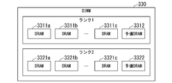
- FIG. 2A shows a configuration example of DIMM 330.
- DIMM330 includes rank 1 and rank 2. When it is not necessary to distinguish between rank 1 and rank 2, it is described as rank.
- the rank indicates a block of memory modules.
- the memory controller 320 manages memory modules in rank units.
- Rank 1 includes a plurality of DRAMs 3311a to 3311c and at least one spare DRAM 3312.
- Rank 2 includes a plurality of DRAMs 3321a to 3321c and at least one spare DRAM 3322. When it is not necessary to distinguish DRAM 3311a to 3311c, it is described as DRAM 3311.
- DRAM 3321 When it is not necessary to distinguish the DRAMs 3321a to 3321c, it is described as the DRAM 3321. Further, when referring to the DRAM included in the DIMM 330 without the need to distinguish the ranks, it is described as DRAM 3301, and when referring to the spare DRAM, it is described as the spare DRAM 3302.
- the number of ranks and the number of DRAMs are not limited to those shown in the figure.
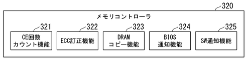
- FIG. 2B shows a configuration example of the memory controller 320.
- the memory controller 320 includes a CE count count function 321, an ECC correction function 322, a DRAM copy function 323, a BIOS notification function 324, and a SW notification function 325.
- the CE count count function 321 counts the number of memory CE occurrences for each DRAM 3301.
- the ECC correction function 322 corrects the ECC (error correction code) when the memory CE occurs in the DRAM 3301.
- the error correction code is a code added so that an error that occurs when recording or transmitting data can be detected and corrected on the receiving side.
- the DRAM copy function 323, for example, copies data from the DRAM 3301 to be switched to the spare DARM 3302 when switching from the DRAM 3301 to the spare DARM 3302.
- the BIOS notification function 324 notifies the FW200 of the occurrence of the memory CE when the number of occurrences of the memory CE exceeds a predetermined threshold value before switching to the spare DARM3302.
- the SW notification function 325 notifies the SW000 (memory error monitoring software 010) of the occurrence of the memory CE when the memory CE further occurs after switching to the spare DARM3302.
- FIG. 3A and 3B are diagrams showing an example of a software group related to a memory error according to an embodiment of the present invention.
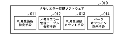
- FIG. 3A shows a configuration example of the memory error monitoring software 010.
- the memory error monitoring software 010 includes a CE occurrence location specifying means 011, a memory error management table reference means 012, a CE occurrence count counting means 013, and a page offline instruction means 014.
- the CE generation location specifying means 011 identifies the DRAM 3301 in which the memory CE is generated.
- the memory error management table reference means 012 refers to the memory error management table 500 described later in FIG. 4, and provides information indicating whether or not data copying to the spare DRAM 3302 has been executed for the DRAM 3301 in which the memory CE has occurred. get.
- the CE occurrence count counting means 013 counts the number of memory CEs notified from the memory controller 320 on a page-by-page basis.
- the page offline instruction means 014 instructs the Kernel 110 to invalidate the page in which the memory CE occurrence count exceeds the threshold value.
- FIG. 3B shows a configuration example of Kernel 110.
- the Kernel 110 has a page data copying means 111 and a page invalidating means 112.
- the page data copying means 111 copies data from the page to be invalidated to a valid page before the page is invalidated.
- the page invalidation means 112 invalidates the page specified by the memory error monitoring software 010 (page offline instruction means 014).
- FIG. 3C shows a configuration example of BIOS210.
- the BIOS 210 includes a CE occurrence location specifying means 211, a memory error management table updating means 212, a DRAM copy instruction means 213, a BIOS notification valid / invalid means 214, and a SW notification valid / invalid means 215.
- the CE generation location specifying means 211 identifies the DRAM 3301 in which the memory CE is generated.
- the memory error management table updating means 212 indicates that the HW function has already been executed for the data corresponding to the position of the DRAM 3301 that has copied the data to the spare DRAM 3302 in the memory error management table 500 described later in FIG. Register the information to be shown.
- the DRAM copy instruction means 213 instructs the memory controller 320 to copy the data of the DRAM 3301 to the spare DRAM 3302 for the DRAM 3301 in which the number of occurrences of the memory CE exceeds the threshold value.
- This instruction is an execution instruction of the HW function.
- the BIOS notification valid / invalid means 214 sets whether or not to notify the BIOS 210 of the occurrence of the memory CE when the memory CE occurs in the DRAM 3301.
- the SW notification valid / invalid means 215 sets whether or not to notify the memory error monitoring software 010 of the occurrence of the memory CE when the memory CE occurs in the DRAM 3301.
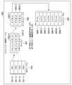
- FIG. 4 is a diagram showing an example of a memory error management table according to an embodiment of the present invention.
- the memory error management table 500 includes a CPU table 501.
- the CPU table 501 includes a memory controller table 502.
- the memory controller table 502 includes a channel table 503.
- the channel table 503 includes a rank table 504.
- FIG. 4 shows the memory of a computer system 400 having four CPU 301s, two memory controllers 302 for each CPU 301, three channels for each memory controller 302, and seven ranks for each CH.
- the error management table 500 is illustrated. As mentioned above, ranks indicate blocks of memory modules.
- the memory error management table 500 includes CPU tables 501-1 to 501-4 corresponding to CPUs 1 to CPU4 (four CPUs 301).
- the CPU table 501-1 corresponding to the CPU 1 includes the memory controller tables 502-1 to 504-2 corresponding to the two memory controllers 302.
- the memory controller table 502-1 includes channel tables 503-1 to 503-3 corresponding to three channels.
- the channel table 503-1 includes rank tables 504-1 to 504-7 corresponding to seven ranks. Then, in each of the rank tables 504-1 to 504-7, the value indicating that the HW function has been executed (for example, 0xFF) or the HW function has not been executed for the memory module of the corresponding block. A value indicating that (for example, 0x00) is stored. In the initial state, the value of "0x00" is stored in each of the rank tables 504-1 to 504-7.
- the BIOS 210 instructs the memory controller 320 to execute the HW function, it writes the value "0xFF" in the rank table 504 (for example, the rank table 504-1) corresponding to the rank including the DRAM 3301.
- the memory error monitoring software 010 gives an instruction to invalidate the page after confirming that the value "0xFF" is stored in the rank table 504. As a result, the order of processing in which the HW function is operated first and then the SW function is operated is secured.
- the BIOS 210 writes to the memory error management table 500 using the memory error management table update means 212.
- the memory error monitoring software 010 uses the memory error management table reference means 012 to read the memory error management table 500. Therefore, the memory error management table 500 is stored in a shared memory or the like accessible by the BIOS 210 and the memory error monitoring software 010.
- FIG. 5 is a first flowchart showing an example of control according to an embodiment of the present invention.
- FIG. 5 shows a process of initializing the notification destination when CE occurs.
- the BIOS 210 sets the memory controller 320 to notify the occurrence of the memory CE to the BIOS 210 by using the BIOS notification valid / invalid means 214 (step S1). Further, the BIOS 210 uses the SW notification valid / invalid means 215 to set the memory controller 320 so as not to notify the SW000 of the occurrence of the memory CE (step S2). Upon receiving these settings, the memory controller 320 sets to enable the BIOS notification function 324 and to disable the SW notification function 325.
- FIG. 6 is a second flowchart showing an example of control according to an embodiment of the present invention.
- the memory controller 320 in which the memory CE is generated corrects the memory CE by using the ECC correction function 322 (step S11).
- the memory controller 320 counts the number of occurrences of the memory CE for each DRAM 3301 by using the CE number counting function 321 (step S12).
- the memory controller 320 confirms whether or not the number of times the memory CE of the DRAM 3301 in which the memory CE has occurred has reached the threshold value (step S13). If the threshold value has not been reached (NO in step S13), the process shown in FIG. 6 ends.
- the memory controller 320 uses the BIOS notification function 324 to notify the BIOS 210 of the occurrence of the memory CE (step S14).
- the occurrence of the memory CE is notified to the BIOS 210, the data of the DRAM 3301 in which the error occurred is first transferred to the spare DRAM 3302 by using the HW function.
- FIG. 7 is a third flowchart showing an example of control according to an embodiment of the present invention.
- FIG. 7 shows the processing when the number of occurrences of the memory CE reaches the threshold value (YES in S13) and the notification is output to the BIOS210 (S14 in FIG. 6).
- the BIOS 210 Upon receiving the notification of the occurrence of the memory CE, the BIOS 210 instructs the memory controller 320 by using the DRAM copy instruction means 213.
- the BIOS 210 instructs the memory controller 320 to copy the data of the DRAM 3301 in which the memory CE is generated to the spare DRAM 3302 (step S21).
- the memory controller 320 operates the HW function by copying the data from the designated DRAM 3301 to the spare DRAM 3302 of the same rank by using the DRAM copy function 323.
- the BIOS 210 uses the CE generation location identifying means 211 to identify the DRAM 3301 in which the memory CE has occurred (step S22).
- the BIOS 210 uses the memory error management table updating means 212 to register the position of the DRAM 3301 in which the memory CE has occurred in the memory error management table 500 (step S23).
- the position of the DRAM 3301 indicates, for example, information for identifying the rank including the DRAM 3301.
- the BIOS 210 is a value indicating that the HW function has been operated (step 1 has been operated) at a location corresponding to "CPU1-memory controller 1-channel 1-rank 1" in the memory error management table 500 shown as an example in FIG. (For example, "0xFF") is registered. That is, the BIOS 210 writes the value "0xFF" in the area corresponding to the rank to which the DRAM 3301 in which the memory CE has occurred belongs in the memory error management table 500.
- the BIOS 210 sets the memory controller 320 so that the memory CE generated at the rank in which the HW function has been operated is not notified to the BIOS 210 by using the BIOS notification valid / invalid means 214 (step S24).
- the BIOS 210 uses the SW notification valid / invalid means 215 to notify the SW000 (memory error monitoring software 010) of the occurrence of the memory CE in any of the plurality of DRAMs 3301s belonging to the rank in which the HW function has been operated. It is set for the controller 320 (step S25).
- FIG. 8 shows a processing flow when the occurrence of the memory CE of the DRAM 3301 belonging to the rank in which the HW function is operated is detected.
- FIG. 8 is a fourth flowchart showing an example of control according to an embodiment of the present invention.
- the memory controller 320 detects the occurrence of the memory CE in any DRAM 3301 belonging to the rank in which the HW function has been operated, the memory controller 320 corrects the memory CE by using the ECC correction function 322 (step S31).
- the memory controller 320 notifies the memory error monitoring software 010 of the occurrence of the memory CE by using the SW notification function 325 based on the fact that the HW function has been operated (without counting the number of CEs) (step). S32).
- the operation of the memory error monitoring software 010 notified of the occurrence of the memory CE will be described with reference to FIG.
- FIG. 9 is a fifth flowchart showing an example of control according to an embodiment of the present invention.
- the memory error monitoring software 010 uses the CE generation location identification means 011 to identify the DRAM 3301 in which the memory CE has occurred (step S41).
- the memory error monitoring software 010 uses the memory error management table reference means 012 to check whether or not the HW function has already been operated for the DRAM 3301 in which the memory CE has occurred, which is specified in step S41 (step 42 and step). S43).
- the memory error monitoring software 010 searches the memory error management table 500 using the position of the DRAM 3301 in which the specified memory CE has occurred as a key, and checks whether or not the HW function has been operated.
- the memory error monitoring software 010 counts the number of CE occurrences on a page-by-page basis using the CE occurrence count counting means 013 (step S44).
- the CE occurrence count counting means 013 counts the CE occurrence count for the page corresponding to the DRAM 3301 identified in step S41 (where the DRAM 3301 is mapped). For example, a plurality of DRAM 3301s are mapped on the page.
- the memory error monitoring software 010 confirms whether or not the number of CE occurrences of the page corresponding to the specified DRAM 3301 has reached the threshold value (step S45).
- the process of FIG. 9 ends.
- the memory error monitoring software 010 uses the page offline instruction means 014 to specify the page to be invalidated and instructs Kernel 110 to page offline (step S46). ..
- the SW function is executed for the page according to the number of CE occurrences of the page to which the DRAM 3301 is mapped.
- the threshold value used in step S45 of FIG. 9 and the threshold value used in step S13 of FIG. 6 may have the same value or different values. That is, the threshold value for determining whether or not to operate the HW function and the threshold value for determining whether or not to operate the SW function may be the same or different.
- FIG. 10 is a sixth flowchart showing an example of control according to an embodiment of the present invention.
- the operation of the Kernel 110 when the page offline is instructed (S46 in FIG. 9) will be described with reference to FIG.
- the Kernel 110 uses the page data copy means 111 to copy the data on the page specified by the memory error monitoring software 010 to another page (step S51).
- the Kernel 110 uses the page invalidation means 112 to invalidate the page in which the memory CE specified by the memory error monitoring software 010 is generated so as not to use it (step S52).
- the SW function has been executed.
- step S22 of FIG. 7 the case where the BIOS 210 specifies that the position of the DRAM in which the memory CE is generated is “CPU1-memory controller 1-channel 1-rank 1” is illustrated.
- step S23 the BIOS 210 has an HW function (data copy to a spare DRAM) at a location corresponding to "CPU1-memory controller 1-channel 1-rank 1" in the memory error management table 500 illustrated in FIG. Register a value that indicates that is already operating.
- the memory error monitoring software 010 specifies that the position of the DRAM 3301 in which the memory CE is generated is “CPU1-memory controller 1-channel 1-rank 1”. That is, the memory error monitoring software 010 identifies the rank of the DRAM 3301 in which the memory CE has occurred. Then, the memory error monitoring software 010 refers to the value of the portion corresponding to "CPU1-memory controller 1-channel 1-rank 1" in the memory error management table 500, and confirms that the HW function has been operated. .. Then, the memory error monitoring software 010 counts the number of memory CE occurrences in step S44.
- the memory error monitoring software 010 When the memory CE occurs in the DRAM 3301 belonging to the rank 1, the memory error monitoring software 010 counts the number of times the memory CE occurs in the page to which the DRAM 3301 is mapped. When the memory error monitoring software 010 has reached the threshold value for the number of memory CE occurrences (YES in step S45), the memory error monitoring software 010 operates the SW function (page offline) for the page in step S46. As described above, in the present embodiment, the SW function is operated after it is confirmed that the HW function has been executed based on the memory error management table 500.
- the memory error management table 500 is created in the FW 200 located between the HW 300 and the SW 000. Further, when the memory CE occurs, the FW200 is notified at first, and the FW200 operates the HW function. Further, the FW 200 registers the position of the DRAM 3301 that operates the HW function in the memory error management table 500. Then, the FW200 is set so that a notification is output to the SW000 when the memory CE is next generated in any DRAM 3301 in the rank in which the HW function has been operated. Further, when memory CE occurs, a notification is output to SW000.
- the SW000 When the SW000 recognizes the memory CE, the DRAM 3301 in which the memory CE has occurred is specified, and the memory error management table 500 is referred to to confirm whether or not the HW function has been operated for the specified DRAM 3301.
- the SW000 operates the page offline function according to the number of memory CE occurrences of the page corresponding to the specified DRAM 3301. As a result, it is possible to realize control in which the HW function is first operated when the memory CE occurs, and the SW function is operated when the memory CE occurs even after the operation of the HW function.
- the HW function operates before the SW function by the setting process (FIG. 5) of the memory CE error notification destination by the BIOS 210.
- the setting process of FIG. 5 the occurrence of the memory CE is notified to the BIOS210, and the SW000 is not notified. Therefore, if the generation of the memory CE is suppressed by the HW function, the SW function (page offline) will not operate. In that case, the operation of the computer system 400 can be continued without being affected by (1) the number of memory pages available to the user is reduced, and (2) the overhead of moving data by the kernel is generated. If it is determined that the memory CE is further generated even after the HW function is operated, the SW function is operated at that time. As a result, memory CEs can be generated at a plurality of locations at the same time, resulting in a UCE (Uncorrectable Error), and the computer system 400 can be prevented from going down.
- UCE Uncorrectable Error
- the memory controller 320 based on the settings of the BIOS notification valid / invalid means 214 and the SW notification valid / invalid means 215 of the BIOS 210, the memory controller 320 notifies the BIOS 210 of the occurrence of the memory CE before the HW function is executed. .. Further, after the HW function is executed, the memory controller 320 notifies the memory error monitoring software 010 that the memory CE has occurred. Further, the position of the DRAM 3301 corresponding to the page requiring invalidation is notified to the memory error monitoring software 010 via the memory error management table 500. Therefore, it is not necessary for the BIOS 210 to notify the page to be invalidated (closed), which is efficient.
- the memory error monitoring software 010 confirms the position of the DRAM 3301 with reference to the memory error management table 500, and invalidates the page corresponding to the confirmed position of the DRAM 3301. As a result, it is not necessary to search the page to be invalidated, which is efficient. Therefore, even in an in-memory computing environment in which the frequency of errors may increase as the memory capacity increases, it is possible to deal with memory failures without delay.
- the memory error management table 500 information on the (limited) DRAM 3301 actually mounted on the computer system 400 is registered. As a result, no matter which DRAM 3301 the memory CE occurs in, the above processing based on the memory error management table 500 can deal with it. Therefore, there are no restrictions such as setting an upper limit on the number of pages that can be invalidated.
- FIG. 11 is a diagram showing a minimum configuration of a memory failure coping system according to an embodiment of the present invention.
- the memory failure handling system 10 includes at least software 20, firmware 30, and a memory controller 40.
- the memory controller 40 detects the occurrence of a memory error (CE)
- the memory controller 40 has an error occurrence notification unit 41 that notifies the firmware 30 or the software 20 of the occurrence of the memory error.
- the software 20 has an invalidation instruction unit 21.
- the invalidation instruction unit 21 instructs the kernel to invalidate the page corresponding to the memory in which the memory error has occurred.
- the firmware 30 has a spare memory switching instruction unit 31 and a notification destination setting unit 32.
- the notification destination setting unit 32 sets the notification destination (software 20 or firmware 30) of the occurrence of the memory error when the memory controller 40 detects the occurrence of the memory error with respect to the memory controller 40.
- the spare memory switching instruction unit 31 receives the notification of the occurrence of the memory error from the memory controller 40, the spare memory switching instruction unit 31 instructs the memory controller 40 to switch from the memory in which the memory error has occurred to the spare memory.
- the software 20 corresponds to the memory error monitoring software 010
- the firmware 30 corresponds to the BIOS 210
- the memory controller 40 corresponds to the memory controller 230.
- the error occurrence notification unit 41 corresponds to the BIOS notification function 324 and the SW notification function 325
- the page invalidation instruction unit 21 corresponds to the page offline instruction means 014.
- the spare memory switching instruction unit 31 corresponds to the DRAM copy instruction means 213
- the notification destination setting unit 32 corresponds to the BIOS notification valid / invalid means 214 and the SW notification valid / invalid means 215.
- the process of each process by each means of the memory error monitoring software 010, each means of Kernel110, and each means of BIOS210 is stored in a computer-readable recording medium in the form of a program.
- the above processing is performed by reading and executing this program by the CPU 310.
- the computer-readable recording medium refers to a magnetic disk, a magneto-optical disk, a CD-ROM, a DVD-ROM, a semiconductor memory, or the like.
- this computer program may be distributed to a computer via a communication line, and the computer receiving the distribution may execute the program.
- the above program may be for realizing a part of the above-mentioned functions.
- a so-called difference file (difference program) may be used, which can realize the above-mentioned functions in combination with a program already recorded in the computer system.
- the computer system 400 is an example of an information processing device.
Landscapes
- Engineering & Computer Science (AREA)
- Theoretical Computer Science (AREA)
- Physics & Mathematics (AREA)
- Quality & Reliability (AREA)
- General Engineering & Computer Science (AREA)
- General Physics & Mathematics (AREA)
- Computing Systems (AREA)
- Mathematical Physics (AREA)
- Techniques For Improving Reliability Of Storages (AREA)
- Detection And Correction Of Errors (AREA)
- Hardware Redundancy (AREA)
- Debugging And Monitoring (AREA)
Abstract
メモリ障害対処システムは、メモリコントローラと、ファームウェアと、ソフトウェアとを含む。メモリコントローラは、メモリエラーの発生を検出すると、通知先の設定に基づいて、メモリエラーの発生をファームウェアまたはソフトウェアへ通知するエラー発生通知手段を有する。ファームウェアは、通知先をメモリコントローラに対して設定する通知先設定手段と、メモリコントローラからメモリエラーの発生を示す通知を受けると、メモリエラーが発生したメモリから予備メモリへの切り替えを指示する予備メモリ切替指示手段とを有する。ソフトウェアは、メモリコントローラからメモリエラーの発生を示す通知を受けると、メモリエラーが発生したメモリに対応するページを無効化する指示を行う無効化指示手段を有する。
Description
本発明は、メモリ障害対処システム、情報処理装置及びメモリ障害対処方法に関する。
近年、DRAM(Dynamic Random Access Memory)の価格の低下、大容量化により、サーバ装置に数十テラバイトのメモリを搭載して、計算に必要なデータをメモリ上に置くことで計算処理を圧倒的に高速化するインメモリ・コンピューティングという技術が利用されている。インメモリ・コンピューティングでは、メモリ上のデータの保全性が重要である。一方、DIMM(Dual Inline Memory Module)の高集積化、大容量化に伴ってエラーの発生頻度も増加している。メモリエラーにはECC(Error Check and Correct)機能で訂正されるCorrectable Error(以下、CEと記載する。)と、ECC機能で訂正できないUncorrectable Error(以下、UCEと記載する。)がある。CEが複数のデータで同時に発生するとECC機能で訂正できないため、UCEとなる。UCEが発生するとシステムダウンが生じる。
これに対し、近年のコンピュータシステムでは、ハードウェア(以下、HWと記載する。)とソフトウェア(以下、SWと記載する。)のそれぞれが、CEが発生した場合の対処機能を装備している。
HWは、あるDRAMでCEの発生回数が閾値に到達した場合、故障と判断して予備のDRAMへデータを移す機能(以下、HW機能と記載する場合がある。)を備えている。
一方、SWは、ページオフラインという機能を装備している。SWは、メモリ上でのCE発生の通知を受けると、ページ単位でCEの発生回数をカウントする。SWは、あるページで発生したCEの発生回数が閾値に到達した場合、そのページを無効化するようカーネルへ指示する。カーネルは、そのページに有効なデータが含まれているがその時点で未使用であれば、別の物理ページへデータを移して、元のページを使用しないように制御する。これをページオフライン機能(以下、SW機能と記載する場合がある。)と呼ぶ。
HWは、あるDRAMでCEの発生回数が閾値に到達した場合、故障と判断して予備のDRAMへデータを移す機能(以下、HW機能と記載する場合がある。)を備えている。
一方、SWは、ページオフラインという機能を装備している。SWは、メモリ上でのCE発生の通知を受けると、ページ単位でCEの発生回数をカウントする。SWは、あるページで発生したCEの発生回数が閾値に到達した場合、そのページを無効化するようカーネルへ指示する。カーネルは、そのページに有効なデータが含まれているがその時点で未使用であれば、別の物理ページへデータを移して、元のページを使用しないように制御する。これをページオフライン機能(以下、SW機能と記載する場合がある。)と呼ぶ。
しかし、一般にHW機能とSW機能は連携して動作しておらず、非効率な動作を行うことがある。例えば、SWが管理対象としているページには、メモリのインターリーブによって、複数のDRAMがマッピングされている。そのため、例えば3つのDRAMそれぞれでCEが発生した場合、SWは、そのページでCEが3回発生したとカウントする。すると、そのページについてSWが管理するCEの発生回数は、HWが個々のDRAMについて管理しているCEの発生回数よりも先に、閾値に到達することがある。すると、HW機能(予備DRAMへのデータコピー)が実行可能であるにも関わらず、SW機能(ページオフライン)が先に動作してしまう。ページオフライン機能が動作すると、(1)ユーザが利用できるメモリページが減る、(2)カーネルによるデータの移動というオーバーヘッドが生じる、といった影響がある。
一方、HW側の機能は、予備のDRAMを使い、HWが有するCOPYエンジンを使ってデータを移す。このため、HW側の機能によるSWへの影響は無い。従って、まずHW側の機能を動作させ、それでもなおメモリCEが発生する場合に、最後の手段として、SW側のページオフラインを動作する方が望ましい。
一方、HW側の機能は、予備のDRAMを使い、HWが有するCOPYエンジンを使ってデータを移す。このため、HW側の機能によるSWへの影響は無い。従って、まずHW側の機能を動作させ、それでもなおメモリCEが発生する場合に、最後の手段として、SW側のページオフラインを動作する方が望ましい。
特許文献1には、このような方針に沿って、HW機能とSW機能とを連動させる仕組みが開示されている。特許文献1は、上記のHWの機能に相当する予備メモリ切替と、上記のSWの機能に相当するページ閉塞とを連携させてシステムダウンを防止するメモリ障害処理システムを開示している。
このメモリ障害処理システムは、メモリCEの発生回数が閾値に達すると、まずメモリCEが発生したメモリを予備メモリに切り替え、その後、メモリCEの発生回数が閾値に達すると、ページ閉塞を行うという制御を行う。これによって、メモリ障害処理システムは、予備メモリ切替とページ閉塞とを連動させている。
ページ閉塞を行うときの動作をより具体的に説明すると、ファームウェア(以下、FWと記載する。)に実装される障害ページ通知部62が、障害が発生した箇所に対応するメモリページを、OS(Operating System)に実装されるページ閉塞部63に通知する。そして、ページ閉塞部63が通知されたページを検索してページ閉塞を行っている。
このメモリ障害処理システムは、メモリCEの発生回数が閾値に達すると、まずメモリCEが発生したメモリを予備メモリに切り替え、その後、メモリCEの発生回数が閾値に達すると、ページ閉塞を行うという制御を行う。これによって、メモリ障害処理システムは、予備メモリ切替とページ閉塞とを連動させている。
ページ閉塞を行うときの動作をより具体的に説明すると、ファームウェア(以下、FWと記載する。)に実装される障害ページ通知部62が、障害が発生した箇所に対応するメモリページを、OS(Operating System)に実装されるページ閉塞部63に通知する。そして、ページ閉塞部63が通知されたページを検索してページ閉塞を行っている。
特許文献1に記載の方法には、次の課題がある。(A)障害ページ通知部62は、BIOS(Basic Input/Output System)と呼ばれるFWに実装されている。BIOSは、エラーが発生したページをテーブルに登録し、ページ毎に発生回数をカウントし、閾値を越えた場合に閾値を越えたページをページ閉塞部63に通知する。OSに実装されるページ閉塞部63は、通知されたページに対してページ閉塞を行う。ただし、BIOSというFWがテーブルの検索、登録、発生回数のカウントを行うため、その処理の間、OSはCPUを使えない。このため、一時的にOSのCPU利用率が下がってしまう。(B)BIOSやOSに上記の機能を実装する以上、無制限に、エラーが発生した全てのページを通知するように実装することはできない。このため、通知するページ数に上限値を設ける必要がある。つまり、障害ページ通知部62は、エラーが発生した全てのページを通知することができず、及び、ページ閉塞部63はエラーが発生した全てのページを閉塞することができないという制約がある。
メモリの大容量化に伴いエラーの発生頻度が増加する可能性のあるインメモリ・コンピューティングに特許文献1の方法を適用すると、上記のような点が制約となってメモリの障害対処ができない。これにより、システムダウン等を招く可能性がある。
そこでこの発明は、上述の課題を解決するメモリ障害対処システム、情報処理装置及びメモリ障害対処方法を提供することを目的としている。
本発明の一態様によれば、メモリ障害対処システムは、メモリコントローラと、ファームウェアと、ソフトウェアと、を含み、前記メモリコントローラは、メモリエラーの発生を検出すると、通知先の設定に基づいて、前記メモリエラーの発生を前記ファームウェアまたは前記ソフトウェアへ通知するエラー発生通知手段を有し、前記ファームウェアは、前記通知先を前記メモリコントローラに対して設定する通知先設定手段と、前記メモリコントローラから前記メモリエラーの発生を示す通知を受けると、前記メモリエラーが発生した前記メモリから予備メモリへの切り替えを指示する予備メモリ切替指示手段と、を有し、前記ソフトウェアは、前記メモリコントローラから前記メモリエラー発生を示す前記通知を受けると、前記メモリエラーが発生した前記メモリに対応するページを無効化する指示を行う無効化指示手段、を有する。
また、本発明の他の一態様によれば、情報処理装置は、上記のメモリ障害対処システムを備える。
また、本発明の他の一態様によれば、メモリ障害対処方法は、ファームウェアが、メモリエラーが発生した場合の通知先をメモリコントローラに対して設定するステップと、前記メモリコントローラが、メモリエラーの発生を検出すると、前記通知先の設定に基づいて、前記メモリエラーの発生を前記ファームウェアまたはソフトウェアへ通知するステップと、前記ファームウェアが、前記メモリコントローラから前記メモリエラー発生を示す通知を受け取った場合、前記メモリエラーが発生したメモリから予備メモリへの切り替えを指示するステップと、前記ソフトウェアが、前記メモリコントローラから前記メモリエラー発生を示す前記通知を受け取った場合、前記メモリエラーが発生した前記メモリに対応するページを無効化する指示を行うステップと、を有する。
本発明によれば、HWによる予備メモリ切り替え機能とSWによるページオフライン機能を連動させて、効果的にメモリCEの発生に対処することができる。
以下、本発明の一実施形態に係るメモリエラー発生時の制御について図面を参照して説明する。
(構成)
図1は、本発明の一実施形態に係るコンピュータシステムの一例を示す図である。
図1に示すように、コンピュータシステム400は、HW(ハードウェア)300と、FW(ファームウェア)200と、OS(オペレーティングシステム)100と、SW(ソフトウェア)000と、を備えている。
(構成)
図1は、本発明の一実施形態に係るコンピュータシステムの一例を示す図である。
図1に示すように、コンピュータシステム400は、HW(ハードウェア)300と、FW(ファームウェア)200と、OS(オペレーティングシステム)100と、SW(ソフトウェア)000と、を備えている。
HW300は、CPU(Central Processing Unit)310と、メモリコントローラ320と、1つ以上のDIMM(Dynamic Random Access Memory)330と、を含む。メモリコントローラ320は、1または複数のチャネル(以降、CHと記載する。)を備える。各DIMM330は何れかのCHに接続されている。DIMM330は、メモリモジュールである。メモリコントローラ320は、DIMM330におけるメモリCE(Correctable Error)の発生を検出する機能と、HW機能(予備DRAMへのデータコピー機能)とを有している。
FW200は、BIOS(Basic Input/Output System)210を含んでいる。BIOS210は、HW300とOS100の間で、HW機能とSW機能を効果的に連携させるための機能を有している。
OS100は、Kernel(カーネル)110を含んでいる。Kernel110は、SW機能(ページのオフライン機能)を有している。
SW000は、メモリエラー監視ソフトウェア010を含んでいる。メモリエラー監視ソフトウェア010は、SW機能の実行を指示する。
SW000は、メモリエラー監視ソフトウェア010を含んでいる。メモリエラー監視ソフトウェア010は、SW機能の実行を指示する。
コンピュータシステム400において、DIMM330にECが発生すると、OS100と、FW200と、HW300とは、連携してメモリエラーへの対処を行う。
図2A及び図2Bは、本発明の一実施形態に係るメモリおよびメモリコントローラの一例を示す図である。
図2Aは、DIMM330の構成例を示す。DIMM330は、ランク1、ランク2を含む。ランク1、ランク2の区別が必要ないときには、ランクと記載する。ランクは、メモリモジュールのブロックを示す。メモリコントローラ320は、ランク単位でメモリモジュールを管理する。ランク1は、複数のDRAM3311a~3311cと、少なくとも1つの予備DRAM3312を備えている。ランク2は、複数のDRAM3321a~3321cと、少なくとも1つの予備DRAM3322を備えている。
なお、DRAM3311a~3311cの区別が必要ないときには、DRAM3311と記載する。DRAM3321a~3321cの区別が必要ないときには、DRAM3321と記載する。また、ランクの区別も必要なくDIMM330に含まれるDRAMを指すときには、DRAM3301と記載し、予備DRAMを指すときには予備DRAM3302と記載する。なお、ランクの数やDRAMの数は、図示するものに限定されない。
図2Aは、DIMM330の構成例を示す。DIMM330は、ランク1、ランク2を含む。ランク1、ランク2の区別が必要ないときには、ランクと記載する。ランクは、メモリモジュールのブロックを示す。メモリコントローラ320は、ランク単位でメモリモジュールを管理する。ランク1は、複数のDRAM3311a~3311cと、少なくとも1つの予備DRAM3312を備えている。ランク2は、複数のDRAM3321a~3321cと、少なくとも1つの予備DRAM3322を備えている。
なお、DRAM3311a~3311cの区別が必要ないときには、DRAM3311と記載する。DRAM3321a~3321cの区別が必要ないときには、DRAM3321と記載する。また、ランクの区別も必要なくDIMM330に含まれるDRAMを指すときには、DRAM3301と記載し、予備DRAMを指すときには予備DRAM3302と記載する。なお、ランクの数やDRAMの数は、図示するものに限定されない。
図2Bは、メモリコントローラ320の構成例を示す。メモリコントローラ320は、CE回数カウント機能321と、ECC訂正機能322と、DRAMコピー機能323と、BIOS通知機能324と、SW通知機能325とを備えている。
CE回数カウント機能321は、DRAM3301ごとにメモリCEの発生回数をカウントする。
ECC訂正機能322は、DRAM3301でメモリCEが発生するとECC(誤り訂正符号)訂正を行う。誤り訂正符号は、データを記録または伝送する際に発生する誤りを、受信側で検出し訂正できるように付加される符号である。
DRAMコピー機能323は、例えば、DRAM3301から予備DARM3302に切り替えるときに、切り替え対象のDRAM3301から予備DARM3302へデータのコピーを行う。例えば、DRAM3311aに閾値回数以上のメモリCEが発生した場合、DRAM3311aから、同じランク1の予備DRAM3312へデータのコピーが実行される。
BIOS通知機能324は、予備DARM3302への切り替え前にメモリCEの発生回数が所定の閾値を上回った場合、メモリCEの発生をFW200へ通知する。
SW通知機能325は、予備DARM3302へ切り替えた後に、さらにメモリCEが発生した場合、メモリCEの発生をSW000(メモリエラー監視ソフトウェア010)へ通知する。
CE回数カウント機能321は、DRAM3301ごとにメモリCEの発生回数をカウントする。
ECC訂正機能322は、DRAM3301でメモリCEが発生するとECC(誤り訂正符号)訂正を行う。誤り訂正符号は、データを記録または伝送する際に発生する誤りを、受信側で検出し訂正できるように付加される符号である。
DRAMコピー機能323は、例えば、DRAM3301から予備DARM3302に切り替えるときに、切り替え対象のDRAM3301から予備DARM3302へデータのコピーを行う。例えば、DRAM3311aに閾値回数以上のメモリCEが発生した場合、DRAM3311aから、同じランク1の予備DRAM3312へデータのコピーが実行される。
BIOS通知機能324は、予備DARM3302への切り替え前にメモリCEの発生回数が所定の閾値を上回った場合、メモリCEの発生をFW200へ通知する。
SW通知機能325は、予備DARM3302へ切り替えた後に、さらにメモリCEが発生した場合、メモリCEの発生をSW000(メモリエラー監視ソフトウェア010)へ通知する。
図3A及び図3Bは、本発明の一実施形態に係るメモリエラーに関するソフトウェア群の一例を示す図である。
図3Aは、メモリエラー監視ソフトウェア010の構成例を示す。メモリエラー監視ソフトウェア010は、CE発生箇所特定手段011と、メモリエラー管理テーブル参照手段012と、CE発生回数カウント手段013と、ページオフライン指示手段014とを有している。
CE発生箇所特定手段011は、メモリCEが発生したDRAM3301を特定する。
メモリエラー管理テーブル参照手段012は、図4で後述するメモリエラー管理テーブル500を参照して、メモリCEが発生したDRAM3301について、予備DRAM3302へのデータコピーが実行済みであるか否かを示す情報を取得する。
CE発生回数カウント手段013は、メモリコントローラ320から通知されたメモリCEの回数をページ単位でカウントする。
ページオフライン指示手段014は、CE発生回数カウント手段013がカウントしたCEの発生回数が閾値を超えると、メモリCEの発生回数が閾値を超えたページを無効化するようにKernel110へ指示する。
図3Aは、メモリエラー監視ソフトウェア010の構成例を示す。メモリエラー監視ソフトウェア010は、CE発生箇所特定手段011と、メモリエラー管理テーブル参照手段012と、CE発生回数カウント手段013と、ページオフライン指示手段014とを有している。
CE発生箇所特定手段011は、メモリCEが発生したDRAM3301を特定する。
メモリエラー管理テーブル参照手段012は、図4で後述するメモリエラー管理テーブル500を参照して、メモリCEが発生したDRAM3301について、予備DRAM3302へのデータコピーが実行済みであるか否かを示す情報を取得する。
CE発生回数カウント手段013は、メモリコントローラ320から通知されたメモリCEの回数をページ単位でカウントする。
ページオフライン指示手段014は、CE発生回数カウント手段013がカウントしたCEの発生回数が閾値を超えると、メモリCEの発生回数が閾値を超えたページを無効化するようにKernel110へ指示する。
図3Bは、Kernel110の構成例を示す。Kernel110は、ページデータコピー手段111と、ページ無効化手段112とを有している。
ページデータコピー手段111は、ページ無効化の前に、無効化対象のページから有効なページへデータをコピーする。
ページ無効化手段112は、メモリエラー監視ソフトウェア010(ページオフライン指示手段014)から指定されたページを無効化する。
ページデータコピー手段111は、ページ無効化の前に、無効化対象のページから有効なページへデータをコピーする。
ページ無効化手段112は、メモリエラー監視ソフトウェア010(ページオフライン指示手段014)から指定されたページを無効化する。
図3Cは、BIOS210の構成例を示す。BIOS210は、CE発生箇所特定手段211と、メモリエラー管理テーブル更新手段212と、DRAMコピー指示手段213と、BIOS通知有効無効手段214と、SW通知有効無効手段215と、を有している。
CE発生箇所特定手段211は、メモリCEが発生したDRAM3301を特定する。
メモリエラー管理テーブル更新手段212は、図4で後述するメモリエラー管理テーブル500内の、予備DRAM3302へデータコピーを行ったDRAM3301の位置に対応するデータに対して、HW機能が実行済みであることを示す情報を登録する。
DRAMコピー指示手段213は、メモリCEの発生回数が閾値を超えたDRAM3301について、そのDRAM3301のデータを予備DRAM3302へコピーするよう、メモリコントローラ320へ指示する。この指示は、HW機能の実行指示である。
BIOS通知有効無効手段214は、DRAM3301でメモリCEが発生した場合に、メモリCEの発生をBIOS210に通知するか否かを設定する。
SW通知有効無効手段215は、DRAM3301でメモリCEが発生した場合に、メモリCEの発生をメモリエラー監視ソフトウェア010に通知するか否かを設定する。
CE発生箇所特定手段211は、メモリCEが発生したDRAM3301を特定する。
メモリエラー管理テーブル更新手段212は、図4で後述するメモリエラー管理テーブル500内の、予備DRAM3302へデータコピーを行ったDRAM3301の位置に対応するデータに対して、HW機能が実行済みであることを示す情報を登録する。
DRAMコピー指示手段213は、メモリCEの発生回数が閾値を超えたDRAM3301について、そのDRAM3301のデータを予備DRAM3302へコピーするよう、メモリコントローラ320へ指示する。この指示は、HW機能の実行指示である。
BIOS通知有効無効手段214は、DRAM3301でメモリCEが発生した場合に、メモリCEの発生をBIOS210に通知するか否かを設定する。
SW通知有効無効手段215は、DRAM3301でメモリCEが発生した場合に、メモリCEの発生をメモリエラー監視ソフトウェア010に通知するか否かを設定する。
図4は、本発明の一実施形態に係るメモリエラー管理テーブルの一例を示す図である。
図4に示すようにメモリエラー管理テーブル500は、CPUテーブル501を含む。CPUテーブル501は、メモリコントローラテーブル502を含む。メモリコントローラテーブル502は、チャネルテーブル503を含む。チャネルテーブル503は、ランクテーブル504を含む。
図4に示すようにメモリエラー管理テーブル500は、CPUテーブル501を含む。CPUテーブル501は、メモリコントローラテーブル502を含む。メモリコントローラテーブル502は、チャネルテーブル503を含む。チャネルテーブル503は、ランクテーブル504を含む。
図4には一例として、4つのCPU301、各CPU301に対して2つのメモリコントローラ302、各メモリコントローラ302に対して3つのCH、各CHに対して7つのランクが設けられたコンピュータシステム400のメモリエラー管理テーブル500を例示する。前述したとおり、ランクはメモリモジュールのブロックを示す。
コンピュータシステム400がこのような構成の場合、図示するように、メモリエラー管理テーブル500は、CPU1~CPU4(4つのCPU301)に対応するCPUテーブル501-1~501-4を含む。また、例えば、CPU1に対応するCPUテーブル501-1は、2つのメモリコントローラ302に対応するメモリコントローラテーブル502-1~502-2を含む。また、例えば、メモリコントローラテーブル502-1は、3つのCHに対応するチャネルテーブル503-1~503-3を含む。また、例えば、チャネルテーブル503-1は、7つのランクに対応するランクテーブル504-1~504-7を含む。
そして、ランクテーブル504-1~504-7の各々には、対応するブロックのメモリモジュールに関して、HW機能が実行済みであることを示す値(例えば、0xFF)、又は、HW機能が未実行であることを示す値(例えば、0x00)が格納される。初期状態では、ランクテーブル504-1~504-7の各々には、「0x00」の値が格納されている。
BIOS210は、メモリコントローラ320に対するHW機能の実行を指示すると、当該DRAM3301を含むランクに対応するランクテーブル504(例えば、ランクテーブル504-1)に値「0xFF」を書き込む。メモリエラー監視ソフトウェア010は、ランクテーブル504に値「0xFF」が格納されていることを確認した後に、ページ無効化の指示を行う。これにより、まず、HW機能を動作し、その後、SW機能を動作させるという処理の順序が確保される。
コンピュータシステム400がこのような構成の場合、図示するように、メモリエラー管理テーブル500は、CPU1~CPU4(4つのCPU301)に対応するCPUテーブル501-1~501-4を含む。また、例えば、CPU1に対応するCPUテーブル501-1は、2つのメモリコントローラ302に対応するメモリコントローラテーブル502-1~502-2を含む。また、例えば、メモリコントローラテーブル502-1は、3つのCHに対応するチャネルテーブル503-1~503-3を含む。また、例えば、チャネルテーブル503-1は、7つのランクに対応するランクテーブル504-1~504-7を含む。
そして、ランクテーブル504-1~504-7の各々には、対応するブロックのメモリモジュールに関して、HW機能が実行済みであることを示す値(例えば、0xFF)、又は、HW機能が未実行であることを示す値(例えば、0x00)が格納される。初期状態では、ランクテーブル504-1~504-7の各々には、「0x00」の値が格納されている。
BIOS210は、メモリコントローラ320に対するHW機能の実行を指示すると、当該DRAM3301を含むランクに対応するランクテーブル504(例えば、ランクテーブル504-1)に値「0xFF」を書き込む。メモリエラー監視ソフトウェア010は、ランクテーブル504に値「0xFF」が格納されていることを確認した後に、ページ無効化の指示を行う。これにより、まず、HW機能を動作し、その後、SW機能を動作させるという処理の順序が確保される。
BIOS210が、メモリエラー管理テーブル更新手段212を使ってメモリエラー管理テーブル500に対する書き込みを行う。メモリエラー監視ソフトウェア010がメモリエラー管理テーブル参照手段012を使って、メモリエラー管理テーブル500の読み込みを行う。従って、メモリエラー管理テーブル500は、BIOS210とメモリエラー監視ソフトウェア010が、アクセス可能な共有メモリ等に記憶される。
(動作)
次にメモリCE発生時の動作について説明する。
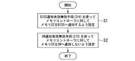
図5は、本発明の一実施形態に係る制御の一例を示す第1のフローチャートである。
図5は、CE発生時の通知先の初期設定を行う処理を示す。
BIOS210は、BIOS通知有効無効手段214を使って、メモリCEの発生をBIOS210へ通知するようメモリコントローラ320に対して設定しておく(ステップS1)。また、BIOS210は、SW通知有効無効手段215を使って、メモリCEの発生をSW000へ通知しないようにメモリコントローラ320に対して設定しておく(ステップS2)。
メモリコントローラ320は、これらの設定を受け取って、BIOS通知機能324を有効にする設定、及び、SW通知機能325を無効にする設定を行う。これらの初期設定により、ECC訂正機能322で訂正されたメモリCEが閾値を越えて発生した場合、その通知は、BIOS通知機能324によって、BIOS210へ通知される。
次に初期設定(図5のS1、S2)が行われた状態でメモリCEが発生したときの動作を、図6を参照して説明する。
次にメモリCE発生時の動作について説明する。
図5は、本発明の一実施形態に係る制御の一例を示す第1のフローチャートである。
図5は、CE発生時の通知先の初期設定を行う処理を示す。
BIOS210は、BIOS通知有効無効手段214を使って、メモリCEの発生をBIOS210へ通知するようメモリコントローラ320に対して設定しておく(ステップS1)。また、BIOS210は、SW通知有効無効手段215を使って、メモリCEの発生をSW000へ通知しないようにメモリコントローラ320に対して設定しておく(ステップS2)。
メモリコントローラ320は、これらの設定を受け取って、BIOS通知機能324を有効にする設定、及び、SW通知機能325を無効にする設定を行う。これらの初期設定により、ECC訂正機能322で訂正されたメモリCEが閾値を越えて発生した場合、その通知は、BIOS通知機能324によって、BIOS210へ通知される。
次に初期設定(図5のS1、S2)が行われた状態でメモリCEが発生したときの動作を、図6を参照して説明する。
図6は、本発明の一実施形態に係る制御の一例を示す第2のフローチャートである。
メモリCEが発生したメモリコントローラ320は、ECC訂正機能322を使ってメモリCEを訂正する(ステップS11)。次にメモリコントローラ320は、CE回数カウント機能321を使って、DRAM3301ごとのメモリCEの発生回数をカウントする(ステップS12)。
メモリコントローラ320は、メモリCEが発生したDRAM3301のメモリCEの発生回数が閾値に到達したか否かを確認する(ステップS13)。閾値に到達していない場合(ステップS13のNO)、図6に示す処理が終了する。閾値に到達した場合(ステップS13のYES)、メモリコントローラ320は、BIOS通知機能324を使って、メモリCEの発生をBIOS210へ通知する(ステップS14)。
メモリCEの発生がBIOS210へ通知されると、始めにHW機能を使ってエラーが発生したDRAM3301のデータが予備DRAM3302へ移される。次に図7を参照してHW機能に係る一連の処理の流れを説明する。
メモリCEが発生したメモリコントローラ320は、ECC訂正機能322を使ってメモリCEを訂正する(ステップS11)。次にメモリコントローラ320は、CE回数カウント機能321を使って、DRAM3301ごとのメモリCEの発生回数をカウントする(ステップS12)。
メモリコントローラ320は、メモリCEが発生したDRAM3301のメモリCEの発生回数が閾値に到達したか否かを確認する(ステップS13)。閾値に到達していない場合(ステップS13のNO)、図6に示す処理が終了する。閾値に到達した場合(ステップS13のYES)、メモリコントローラ320は、BIOS通知機能324を使って、メモリCEの発生をBIOS210へ通知する(ステップS14)。
メモリCEの発生がBIOS210へ通知されると、始めにHW機能を使ってエラーが発生したDRAM3301のデータが予備DRAM3302へ移される。次に図7を参照してHW機能に係る一連の処理の流れを説明する。
図7は、本発明の一実施形態に係る制御の一例を示す第3のフローチャートである。図7は、メモリCEの発生回数が閾値に達し(S13のYES)、BIOS210に通知が出力された場合(図6のS14)の処理を示す。
メモリCE発生の通知を受信したBIOS210は、DRAMコピー指示手段213を使ってメモリコントローラ320に対して指示する。BIOS210は、メモリCEが発生したDRAM3301のデータを予備DRAM3302へコピーするよう、メモリコントローラ320に対して指示する(ステップS21)。メモリコントローラ320は、この指示を受けて、DRAMコピー機能323を使って、指定されたDRAM3301から同じランクの予備DRAM3302へのデータのコピーを行うことで、HW機能を動作させる。
次にBIOS210は、CE発生箇所特定手段211を使って、メモリCEが発生したDRAM3301を特定する(ステップS22)。次にBIOS210は、メモリエラー管理テーブル更新手段212を使って、メモリCEが発生したDRAM3301の位置を、メモリエラー管理テーブル500に登録する(ステップS23)。DRAM3301の位置は、例えば、当該DRAM3301を含むランクを識別する情報を示す。
ここで、例えば、メモリCEが発生したDRAMの位置が、「CPU1-メモリコントローラ1-チャネル1-ランク1」であった場合を例示する。この場合、BIOS210は、図4に例示で示されるメモリエラー管理テーブル500の「CPU1-メモリコントローラ1-チャネル1-ランク1」に該当する箇所にHW機能動作済み(ステップ1動作済み)を示す値(例えば、「0xFF」)を登録する。すなわち、BIOS210は、メモリエラー管理テーブル500における、メモリCEが発生したDRAM3301が属するランクに対応するエリアに値「0xFF」を書き込む。
次に、BIOS210は、BIOS通知有効無効手段214を使って、HW機能が動作済みのランクで発生したメモリCEをBIOS210へ通知しないよう、メモリコントローラ320に対して設定する(ステップS24)。BIOS210は、SW通知有効無効手段215を使って、HW機能が動作済みのランクに属する複数のDRAM3301の何れかのDRAM3301におけるメモリCEの発生をSW000(メモリエラー監視ソフトウェア010)へ通知するよう、メモリコントローラ320に対して設定する(ステップS25)。
これにより、HW機能を動作させたランクに属する複数のDRAM3301のうち、その後、他のDRAM3301等でメモリCEが発生した場合に、そのメモリCEの発生はメモリエラー監視ソフトウェア010へ通知される。これは、同一ランクに属する複数のDRAM3301のうち、何れかのDRAM3301に対してHW機能が既に動作済みの場合、予備DRAM3302が無いという理由により、SW機能で対処する必要があるためである。メモリCEの発生回数は、メモリエラー監視ソフトウェア010でカウントされ、閾値を上回った場合(図9にて後述)、SW機能を使って、エラーが発生したページのデータが別のページに移される。
次に、HW機能が動作したランクに属するDRAM3301のメモリCEの発生が検出された場合の処理の流れを図8に示す。
メモリCE発生の通知を受信したBIOS210は、DRAMコピー指示手段213を使ってメモリコントローラ320に対して指示する。BIOS210は、メモリCEが発生したDRAM3301のデータを予備DRAM3302へコピーするよう、メモリコントローラ320に対して指示する(ステップS21)。メモリコントローラ320は、この指示を受けて、DRAMコピー機能323を使って、指定されたDRAM3301から同じランクの予備DRAM3302へのデータのコピーを行うことで、HW機能を動作させる。
次にBIOS210は、CE発生箇所特定手段211を使って、メモリCEが発生したDRAM3301を特定する(ステップS22)。次にBIOS210は、メモリエラー管理テーブル更新手段212を使って、メモリCEが発生したDRAM3301の位置を、メモリエラー管理テーブル500に登録する(ステップS23)。DRAM3301の位置は、例えば、当該DRAM3301を含むランクを識別する情報を示す。
ここで、例えば、メモリCEが発生したDRAMの位置が、「CPU1-メモリコントローラ1-チャネル1-ランク1」であった場合を例示する。この場合、BIOS210は、図4に例示で示されるメモリエラー管理テーブル500の「CPU1-メモリコントローラ1-チャネル1-ランク1」に該当する箇所にHW機能動作済み(ステップ1動作済み)を示す値(例えば、「0xFF」)を登録する。すなわち、BIOS210は、メモリエラー管理テーブル500における、メモリCEが発生したDRAM3301が属するランクに対応するエリアに値「0xFF」を書き込む。
次に、BIOS210は、BIOS通知有効無効手段214を使って、HW機能が動作済みのランクで発生したメモリCEをBIOS210へ通知しないよう、メモリコントローラ320に対して設定する(ステップS24)。BIOS210は、SW通知有効無効手段215を使って、HW機能が動作済みのランクに属する複数のDRAM3301の何れかのDRAM3301におけるメモリCEの発生をSW000(メモリエラー監視ソフトウェア010)へ通知するよう、メモリコントローラ320に対して設定する(ステップS25)。
これにより、HW機能を動作させたランクに属する複数のDRAM3301のうち、その後、他のDRAM3301等でメモリCEが発生した場合に、そのメモリCEの発生はメモリエラー監視ソフトウェア010へ通知される。これは、同一ランクに属する複数のDRAM3301のうち、何れかのDRAM3301に対してHW機能が既に動作済みの場合、予備DRAM3302が無いという理由により、SW機能で対処する必要があるためである。メモリCEの発生回数は、メモリエラー監視ソフトウェア010でカウントされ、閾値を上回った場合(図9にて後述)、SW機能を使って、エラーが発生したページのデータが別のページに移される。
次に、HW機能が動作したランクに属するDRAM3301のメモリCEの発生が検出された場合の処理の流れを図8に示す。
図8は、本発明の一実施形態に係る制御の一例を示す第4のフローチャートである。
メモリコントローラ320は、HW機能が動作済みのランクに属する何れかのDRAM3301におけるメモリCEの発生を検出すると、ECC訂正機能322を使ってメモリCEを訂正する(ステップS31)。次にメモリコントローラ320は、HW機能動作済みであることに基づいて(CE回数をカウントせずに)、SW通知機能325を使って、メモリCEの発生をメモリエラー監視ソフトウェア010へ通知する(ステップS32)。メモリCEの発生が通知されたメモリエラー監視ソフトウェア010の動作を、図9を参照して説明する。
メモリコントローラ320は、HW機能が動作済みのランクに属する何れかのDRAM3301におけるメモリCEの発生を検出すると、ECC訂正機能322を使ってメモリCEを訂正する(ステップS31)。次にメモリコントローラ320は、HW機能動作済みであることに基づいて(CE回数をカウントせずに)、SW通知機能325を使って、メモリCEの発生をメモリエラー監視ソフトウェア010へ通知する(ステップS32)。メモリCEの発生が通知されたメモリエラー監視ソフトウェア010の動作を、図9を参照して説明する。
図9は、本発明の一実施形態に係る制御の一例を示す第5のフローチャートである。
メモリエラー監視ソフトウェア010は、CE発生箇所特定手段011を使って、メモリCEが発生したDRAM3301を特定する(ステップS41)。次にメモリエラー監視ソフトウェア010は、メモリエラー管理テーブル参照手段012を使って、ステップS41で特定した、メモリCEが発生したDRAM3301に対してHW機能が動作済みか否かを調べる(ステップ42及びステップS43)。具体的には、メモリエラー監視ソフトウェア010は、特定したメモリCEが発生したDRAM3301の位置をキーにして、メモリエラー管理テーブル500を検索して、HW機能が動作済みか否かを調べる。
HW機能がまだ動作していない場合は(ステップS43のNO)、図9の処理が終了する。HW機能が動作済みの場合(ステップS43のYES)、メモリエラー監視ソフトウェア010は、CE発生回数カウント手段013を使ってCE発生回数をページ単位でカウントする(ステップS44)。CE発生回数カウント手段013は、ステップS41で特定されたDRAM3301に対応する(DRAM3301がマッピングされた)ページについてCE発生回数をカウントする。例えば、ページには、複数のDRAM3301がマッピングされている。
メモリエラー監視ソフトウェア010は、特定されたDRAM3301に対応するページのCE発生回数が閾値に到達したか否かを確認する(ステップS45)。閾値に到達していない場合(ステップS45のNO)、図9の処理が終了する。閾値に到達した場合(ステップS45のYES)、メモリエラー監視ソフトウェア010は、ページオフライン指示手段014を使って、無効化するページを指定して、ページオフラインをKernel110に対して指示する(ステップS46)。
このように、エラーが発生したDRAM3301のランク内でHW機能が動作済みの場合には、当該DRAM3301がマッピングされたページのCE発生回数に応じて、当該ページに対してSW機能が実行される。なお、図9のステップS45で用いられる閾値と、図6のステップS13で用いられる閾値は同一の値であってもよいし、異なる値であってもよい。すなわち、HW機能を動作させるか否かを判定するための閾値と、SW機能を動作させるか否かの閾値は、同一であってもよいし異なっていてもよい。
メモリエラー監視ソフトウェア010は、CE発生箇所特定手段011を使って、メモリCEが発生したDRAM3301を特定する(ステップS41)。次にメモリエラー監視ソフトウェア010は、メモリエラー管理テーブル参照手段012を使って、ステップS41で特定した、メモリCEが発生したDRAM3301に対してHW機能が動作済みか否かを調べる(ステップ42及びステップS43)。具体的には、メモリエラー監視ソフトウェア010は、特定したメモリCEが発生したDRAM3301の位置をキーにして、メモリエラー管理テーブル500を検索して、HW機能が動作済みか否かを調べる。
HW機能がまだ動作していない場合は(ステップS43のNO)、図9の処理が終了する。HW機能が動作済みの場合(ステップS43のYES)、メモリエラー監視ソフトウェア010は、CE発生回数カウント手段013を使ってCE発生回数をページ単位でカウントする(ステップS44)。CE発生回数カウント手段013は、ステップS41で特定されたDRAM3301に対応する(DRAM3301がマッピングされた)ページについてCE発生回数をカウントする。例えば、ページには、複数のDRAM3301がマッピングされている。
メモリエラー監視ソフトウェア010は、特定されたDRAM3301に対応するページのCE発生回数が閾値に到達したか否かを確認する(ステップS45)。閾値に到達していない場合(ステップS45のNO)、図9の処理が終了する。閾値に到達した場合(ステップS45のYES)、メモリエラー監視ソフトウェア010は、ページオフライン指示手段014を使って、無効化するページを指定して、ページオフラインをKernel110に対して指示する(ステップS46)。
このように、エラーが発生したDRAM3301のランク内でHW機能が動作済みの場合には、当該DRAM3301がマッピングされたページのCE発生回数に応じて、当該ページに対してSW機能が実行される。なお、図9のステップS45で用いられる閾値と、図6のステップS13で用いられる閾値は同一の値であってもよいし、異なる値であってもよい。すなわち、HW機能を動作させるか否かを判定するための閾値と、SW機能を動作させるか否かの閾値は、同一であってもよいし異なっていてもよい。
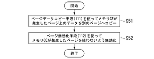
図10は、本発明の一実施形態に係る制御の一例を示す第6のフローチャートである。図10を参照して、ページオフラインを指示された(図9のS46)ときの、Kernel110の動作を説明する。
Kernel110は、ページデータコピー手段111を使って、メモリエラー監視ソフトウェア010から指定されたページ上のデータを別のページへコピーする(ステップS51)。次にKernel110は、ページ無効化手段112を使って、メモリエラー監視ソフトウェア010から指定されたメモリCEが発生したページを使わないよう無効化する(ステップS52)。これにより、SW機能が実行済みとなる。
Kernel110は、ページデータコピー手段111を使って、メモリエラー監視ソフトウェア010から指定されたページ上のデータを別のページへコピーする(ステップS51)。次にKernel110は、ページ無効化手段112を使って、メモリエラー監視ソフトウェア010から指定されたメモリCEが発生したページを使わないよう無効化する(ステップS52)。これにより、SW機能が実行済みとなる。
次にメモリエラー管理テーブル500の登録と参照について、具体例を交えて説明する。
例えば、図7のステップS22において、BIOS210が、メモリCEが発生したDRAMの位置が、「CPU1-メモリコントローラ1-チャネル1-ランク1」であると特定する場合を例示する。この場合、ステップS23において、BIOS210は、図4に例示するメモリエラー管理テーブル500の「CPU1-メモリコントローラ1-チャネル1-ランク1」に該当する箇所に、HW機能(予備DRAMへのデータコピー)が動作済みであることを示す値を登録する。
そして、図9の処理のステップS41において、メモリエラー監視ソフトウェア010は、メモリCEが発生したDRAM3301の位置が、「CPU1-メモリコントローラ1-チャネル1-ランク1」であると特定する。すなわち、メモリエラー監視ソフトウェア010は、メモリCEが発生したDRAM3301のランクを識別する。そして、メモリエラー監視ソフトウェア010は、メモリエラー管理テーブル500の「CPU1-メモリコントローラ1-チャネル1-ランク1」に該当する箇所の値を参照して、HW機能が動作済みであることを確認する。
そして、メモリエラー監視ソフトウェア010は、ステップS44においてメモリCE発生回数をカウントする。メモリエラー監視ソフトウェア010は、ランク1に属するDRAM3301でメモリCEが発生した場合、当該DRAM3301がマッピングされたページのメモリCE発生回数をカウントする。メモリエラー監視ソフトウェア010は、メモリCE発生回数が閾値に到達していた場合(ステップS45のYES)、ステップS46において、当該ページについてSW機能(ページオフライン)を動作させる。このように本実施形態では、メモリエラー管理テーブル500に基づいて、HW機能が実行済みであることが確認されてから、SW機能を動作させる。
例えば、図7のステップS22において、BIOS210が、メモリCEが発生したDRAMの位置が、「CPU1-メモリコントローラ1-チャネル1-ランク1」であると特定する場合を例示する。この場合、ステップS23において、BIOS210は、図4に例示するメモリエラー管理テーブル500の「CPU1-メモリコントローラ1-チャネル1-ランク1」に該当する箇所に、HW機能(予備DRAMへのデータコピー)が動作済みであることを示す値を登録する。
そして、図9の処理のステップS41において、メモリエラー監視ソフトウェア010は、メモリCEが発生したDRAM3301の位置が、「CPU1-メモリコントローラ1-チャネル1-ランク1」であると特定する。すなわち、メモリエラー監視ソフトウェア010は、メモリCEが発生したDRAM3301のランクを識別する。そして、メモリエラー監視ソフトウェア010は、メモリエラー管理テーブル500の「CPU1-メモリコントローラ1-チャネル1-ランク1」に該当する箇所の値を参照して、HW機能が動作済みであることを確認する。
そして、メモリエラー監視ソフトウェア010は、ステップS44においてメモリCE発生回数をカウントする。メモリエラー監視ソフトウェア010は、ランク1に属するDRAM3301でメモリCEが発生した場合、当該DRAM3301がマッピングされたページのメモリCE発生回数をカウントする。メモリエラー監視ソフトウェア010は、メモリCE発生回数が閾値に到達していた場合(ステップS45のYES)、ステップS46において、当該ページについてSW機能(ページオフライン)を動作させる。このように本実施形態では、メモリエラー管理テーブル500に基づいて、HW機能が実行済みであることが確認されてから、SW機能を動作させる。
本実施形態によれば、HW300とSW000の中間に位置するFW200にメモリエラー管理テーブル500を作成しておく。また、メモリCEが発生すると最初はFW200に通知が行き、FW200がHW機能を動作させる。さらにFW200はHW機能を動作させたDRAM3301の位置をメモリエラー管理テーブル500に登録する。
そして、FW200は、HW機能が動作済みのランク内の何れかのDRAM3301で次にメモリCEが発生した場合、SW000に通知が出力されるように設定する。さらにメモリCEが発生するとSW000に通知が出力される。SW000がメモリCEを認識すると、メモリCEが発生したDRAM3301を特定し、メモリエラー管理テーブル500を参照して、特定したDRAM3301に対してHW機能が動作済みか否かを確認する。HW機能が動作済みの場合、SW000は、特定したDRAM3301に対応するページのメモリCE発生回数に応じてページオフライン機能を動作させる。
これにより、メモリCEが発生した場合にまずHW機能を動作させ、HW機能の動作後においてもメモリCEが発生する場合にSW機能を動作させるという制御を実現することができる。
そして、FW200は、HW機能が動作済みのランク内の何れかのDRAM3301で次にメモリCEが発生した場合、SW000に通知が出力されるように設定する。さらにメモリCEが発生するとSW000に通知が出力される。SW000がメモリCEを認識すると、メモリCEが発生したDRAM3301を特定し、メモリエラー管理テーブル500を参照して、特定したDRAM3301に対してHW機能が動作済みか否かを確認する。HW機能が動作済みの場合、SW000は、特定したDRAM3301に対応するページのメモリCE発生回数に応じてページオフライン機能を動作させる。
これにより、メモリCEが発生した場合にまずHW機能を動作させ、HW機能の動作後においてもメモリCEが発生する場合にSW機能を動作させるという制御を実現することができる。
また、上記したように、本実施形態によれば、BIOS210によるメモリCEエラーの通知先の設定処理(図5)により、SW機能より先にHW機能が動作する。図5の設定処理では、メモリCEの発生がBIOS210に対して通知され、SW000には通知されないように設定される。そのため、HW機能によってメモリCEの発生が収まれば、SW機能(ページオフライン)が動作することはない。その場合、(1)ユーザが利用できるメモリページが減る、(2)カーネルによるデータの移動というオーバーヘッドが生じる、といった影響を受けることなく、コンピュータシステム400の運用を継続することができる。
HW機能が動作した後であってもさらにメモリCEが発生していると判定された場合には、その時点で、SW機能を動作させる。これにより、メモリCEが複数個所で同時に発生しUCE(Uncorrectable Error)となり、コンピュータシステム400がシステムダウンすることを防止できる。
HW機能が動作した後であってもさらにメモリCEが発生していると判定された場合には、その時点で、SW機能を動作させる。これにより、メモリCEが複数個所で同時に発生しUCE(Uncorrectable Error)となり、コンピュータシステム400がシステムダウンすることを防止できる。
また、本実施形態では、BIOS210のBIOS通知有効無効手段214、及びSW通知有効無効手段215の設定に基づいて、HW機能実行前であれば、メモリコントローラ320からBIOS210へメモリCE発生が通知される。また、HW機能実行後であれば、メモリコントローラ320からメモリエラー監視ソフトウェア010へメモリCE発生が通知される。また、無効化が必要なページに対応するDRAM3301の位置は、メモリエラー管理テーブル500を介してメモリエラー監視ソフトウェア010に通知される。そのため、BIOS210が無効化(閉塞)すべきページを通知する必要が無く効率的である。
また、メモリエラー監視ソフトウェア010は、メモリエラー管理テーブル500を参照してDRAM3301の位置を確認し、確認されたDRAM3301の位置に対応するページを無効化する。これにより、無効化対象のページを検索する必要が無く効率的である。
従って、メモリの大容量化に伴いエラーの発生頻度が増加する可能性のあるインメモリ・コンピューティング環境においても、滞りなく、メモリ障害への対処を行うことができる。
また、メモリエラー監視ソフトウェア010は、メモリエラー管理テーブル500を参照してDRAM3301の位置を確認し、確認されたDRAM3301の位置に対応するページを無効化する。これにより、無効化対象のページを検索する必要が無く効率的である。
従って、メモリの大容量化に伴いエラーの発生頻度が増加する可能性のあるインメモリ・コンピューティング環境においても、滞りなく、メモリ障害への対処を行うことができる。
また、メモリエラー管理テーブル500には、コンピュータシステム400が実際に搭載する(有限の)DRAM3301の情報を登録しておく。これにより、どのDRAM3301でメモリCEが発生した場合であっても、メモリエラー管理テーブル500に基づく上記処理により対処することができる。従って、無効化できるページ数に上限値を設ける等の制約が生じない。
図11は、本発明の一実施形態に係るメモリ障害対処システムの最小構成を示す図である。
図11に示すようにメモリ障害対処システム10は、少なくともソフトウェア20と、ファームウェア30と、メモリコントローラ40とを含む。
メモリコントローラ40は、メモリエラー(CE)の発生を検出すると、メモリエラーの発生を、ファームウェア30またはソフトウェア20へ通知するエラー発生通知部41を有する。
ソフトウェア20は、無効化指示部21を有する。無効化指示部21は、メモリコントローラ320からメモリエラー発生の通知を受けると、メモリエラーが発生したメモリに対応するページを無効化するようカーネルに指示する。
ファームウェア30は、予備メモリ切替指示部31と通知先設定部32とを有する。通知先設定部32は、メモリコントローラ40がメモリエラーの発生を検出した時のメモリエラー発生の通知先(ソフトウェア20またはファームウェア30)を、メモリコントローラ40に対して設定する。予備メモリ切替指示部31は、メモリコントローラ40からメモリエラー発生の通知を受けると、メモリエラーが発生したメモリから予備メモリへの切り替えをメモリコントローラ40へ指示する。
上記の実施形態の構成と対比すると、ソフトウェア20はメモリエラー監視ソフトウェア010に対応し、ファームウェア30はBIOS210に対応し、メモリコントローラ40はメモリコントローラ230に対応する。
また、エラー発生通知部41はBIOS通知機能324およびSW通知機能325に対応し、ページ無効化指示部21はページオフライン指示手段014に対応する。また、予備メモリ切替指示部31はDRAMコピー指示手段213に対応し、通知先設定部32はBIOS通知有効無効手段214およびSW通知有効無効手段215に対応する。
図11に示すようにメモリ障害対処システム10は、少なくともソフトウェア20と、ファームウェア30と、メモリコントローラ40とを含む。
メモリコントローラ40は、メモリエラー(CE)の発生を検出すると、メモリエラーの発生を、ファームウェア30またはソフトウェア20へ通知するエラー発生通知部41を有する。
ソフトウェア20は、無効化指示部21を有する。無効化指示部21は、メモリコントローラ320からメモリエラー発生の通知を受けると、メモリエラーが発生したメモリに対応するページを無効化するようカーネルに指示する。
ファームウェア30は、予備メモリ切替指示部31と通知先設定部32とを有する。通知先設定部32は、メモリコントローラ40がメモリエラーの発生を検出した時のメモリエラー発生の通知先(ソフトウェア20またはファームウェア30)を、メモリコントローラ40に対して設定する。予備メモリ切替指示部31は、メモリコントローラ40からメモリエラー発生の通知を受けると、メモリエラーが発生したメモリから予備メモリへの切り替えをメモリコントローラ40へ指示する。
上記の実施形態の構成と対比すると、ソフトウェア20はメモリエラー監視ソフトウェア010に対応し、ファームウェア30はBIOS210に対応し、メモリコントローラ40はメモリコントローラ230に対応する。
また、エラー発生通知部41はBIOS通知機能324およびSW通知機能325に対応し、ページ無効化指示部21はページオフライン指示手段014に対応する。また、予備メモリ切替指示部31はDRAMコピー指示手段213に対応し、通知先設定部32はBIOS通知有効無効手段214およびSW通知有効無効手段215に対応する。
なお、メモリエラー監視ソフトウェア010の各手段、Kernel110の各手段、及びBIOS210の各手段による各処理の過程は、プログラムの形式でコンピュータ読み取り可能な記録媒体に記憶される。このプログラムが、CPU310が読み出して実行することによって、上記処理が行われる。ここでコンピュータ読み取り可能な記録媒体とは、磁気ディスク、光磁気ディスク、CD-ROM、DVD-ROM、半導体メモリ等をいう。また、このコンピュータプログラムを通信回線によってコンピュータに配信し、この配信を受けたコンピュータが当該プログラムを実行するようにしてもよい。また、上記プログラムは、前述した機能の一部を実現するためのものであってもよい。さらに、前述した機能をコンピュータシステムにすでに記録されているプログラムとの組み合わせで実現できるもの、いわゆる差分ファイル(差分プログラム)であってもよい。
その他、本発明の趣旨を逸脱しない範囲で、上記した実施の形態における構成要素を周知の構成要素に置き換えることは適宜可能である。また、この発明の技術範囲は上記の実施形態に限られるものではなく、本発明の趣旨を逸脱しない範囲において種々の変更を加えることが可能である。コンピュータシステム400は、情報処理装置の一例である。
この出願は、2019年3月19日に日本出願された特願2019-051453号を基礎とする優先権を主張し、その開示の全てをここに取り込む。
本発明によれば、HWによる予備メモリ切り替え機能とSWによるページオフライン機能を連動させて、効果的にメモリCEの発生に対処することができる。
000・・・SW
010・・・メモリエラー監視ソフトウェア
011・・・CE発生箇所特定手段
012・・・メモリエラー管理テーブル参照手段
013・・・CE発生回数カウント手段
014・・・ページオフライン指示手段
100・・・OS
110・・・Kernel
111・・・ページデータコピー手段
112・・・ページ無効化手段
200・・・FW
210・・・BIOS
211・・・CE発生箇所特定手段
212・・・メモリエラー管理テーブル更新手段
213・・・DRAMコピー指示手段
214・・・BIOS通知有効無効手段
215・・・SW通知有効無効手段
300・・・HW
310・・・CPU
320・・・メモリコントローラ
321・・・CE回数カウント機能
322・・・ECC訂正機能
323・・・DRAMコピー機能
324・・・BIOS通知機能
325・・・SW通知機能
330・・・DIMM
3311、3321・・・DRAM
400・・・コンピュータシステム
500・・・メモリエラー管理テーブル
501・・・CPUテーブル
502・・・メモリコントローラテーブル
503・・・チャネルテーブル
504・・・ランクテーブル
010・・・メモリエラー監視ソフトウェア
011・・・CE発生箇所特定手段
012・・・メモリエラー管理テーブル参照手段
013・・・CE発生回数カウント手段
014・・・ページオフライン指示手段
100・・・OS
110・・・Kernel
111・・・ページデータコピー手段
112・・・ページ無効化手段
200・・・FW
210・・・BIOS
211・・・CE発生箇所特定手段
212・・・メモリエラー管理テーブル更新手段
213・・・DRAMコピー指示手段
214・・・BIOS通知有効無効手段
215・・・SW通知有効無効手段
300・・・HW
310・・・CPU
320・・・メモリコントローラ
321・・・CE回数カウント機能
322・・・ECC訂正機能
323・・・DRAMコピー機能
324・・・BIOS通知機能
325・・・SW通知機能
330・・・DIMM
3311、3321・・・DRAM
400・・・コンピュータシステム
500・・・メモリエラー管理テーブル
501・・・CPUテーブル
502・・・メモリコントローラテーブル
503・・・チャネルテーブル
504・・・ランクテーブル
Claims (8)
- メモリコントローラと、
ファームウェアと、
ソフトウェアと、
を含み、
前記メモリコントローラは、
メモリエラーの発生を検出すると、通知先の設定に基づいて、前記メモリエラーの発生を前記ファームウェアまたは前記ソフトウェアへ通知するエラー発生通知手段、を有し、
前記ファームウェアは、
前記通知先を前記メモリコントローラに対して設定する通知先設定手段と、
前記メモリコントローラから前記メモリエラーの発生を示す通知を受けると、前記メモリエラーが発生した前記メモリから予備メモリへの切り替えを指示する予備メモリ切替指示手段と、を有し、
前記ソフトウェアは、
前記メモリコントローラから前記メモリエラーの発生を示す前記通知を受けると、前記メモリエラーが発生した前記メモリに対応するページを無効化する指示を行う無効化指示手段、を有する、
メモリ障害対処システム。 - 前記通知先設定手段は、前記予備メモリへの前記切り替え前においては、前記ファームウェアを前記通知先として設定し、前記予備メモリへの前記切り替え後には、前記ソフトウェアを前記通知先として設定する、
請求項1に記載のメモリ障害対処システム。 - 前記ファームウェアは、前記メモリコントローラが管理する複数のメモリについて、前記予備メモリへ切り替え済みか否かを示す情報を登録するメモリエラー管理テーブルを記憶し、
前記メモリエラー管理テーブルは、前記ファームウェアから更新可能、且つ、前記ソフトウェアから参照可能に記憶される、
請求項1または請求項2に記載のメモリ障害対処システム。 - 前記ファームウェアは、前記予備メモリへの前記切り替えを指示すると、切り替え対象の前記メモリが、前記予備メモリへ切り替え済みであること示す情報を前記メモリエラー管理テーブルに登録する、
請求項3に記載のメモリ障害対処システム。 - 前記ソフトウェアは、前記メモリエラー管理テーブルを参照して、前記メモリエラーが発生したメモリについて、前記切り替え済みであること示す情報が登録されている場合に、前記ページの無効化を指示する、
請求項3または請求項4に記載のメモリ障害対処システム。 - 前記ソフトウェアは、前記メモリエラー管理テーブルに登録された前記メモリの位置に基づいて、当該位置に対応する前記ページの無効化を指示する、
請求項3から請求項5の何れか1項に記載のメモリ障害対処システム。 - 請求項1から請求項6の何れか1項に記載のメモリ障害対処システムを含む、
情報処理装置。 - ファームウェアが、メモリエラーが発生した場合の通知先をメモリコントローラに対して設定するステップと、
前記メモリコントローラが、メモリエラーの発生を検出すると、前記通知先の設定に基づいて、前記メモリエラーの発生を前記ファームウェアまたはソフトウェアへ通知するステップと、
前記ファームウェアが、前記メモリコントローラから前記メモリエラーの発生を示す通知を受け取った場合、前記メモリエラーが発生したメモリから予備メモリへの切り替えを指示するステップと、
前記ソフトウェアが、前記メモリコントローラから前記メモリエラーの発生を示す前記通知を受け取った場合、前記メモリエラーが発生した前記メモリに対応するページを無効化する指示を行うステップと
を有する、メモリ障害対処方法。
Priority Applications (1)
| Application Number | Priority Date | Filing Date | Title |
|---|---|---|---|
| US17/437,193 US11726888B2 (en) | 2019-03-19 | 2020-03-16 | Memory fault handling system, information processing device, and memory fault handling method |
Applications Claiming Priority (2)
| Application Number | Priority Date | Filing Date | Title |
|---|---|---|---|
| JP2019-051453 | 2019-03-19 | ||
| JP2019051453A JP6679122B1 (ja) | 2019-03-19 | 2019-03-19 | メモリ障害対処システム、情報処理装置及びメモリ障害対処方法 |
Publications (1)
| Publication Number | Publication Date |
|---|---|
| WO2020189617A1 true WO2020189617A1 (ja) | 2020-09-24 |
Family
ID=70166575
Family Applications (1)
| Application Number | Title | Priority Date | Filing Date |
|---|---|---|---|
| PCT/JP2020/011396 Ceased WO2020189617A1 (ja) | 2019-03-19 | 2020-03-16 | メモリ障害対処システム、情報処理装置及びメモリ障害対処方法 |
Country Status (3)
| Country | Link |
|---|---|
| US (1) | US11726888B2 (ja) |
| JP (1) | JP6679122B1 (ja) |
| WO (1) | WO2020189617A1 (ja) |
Cited By (1)
| Publication number | Priority date | Publication date | Assignee | Title |
|---|---|---|---|---|
| US12019503B2 (en) | 2022-05-18 | 2024-06-25 | Samsung Electronics Co., Ltd. | Systems and methods for expandable memory error handling |
Families Citing this family (1)
| Publication number | Priority date | Publication date | Assignee | Title |
|---|---|---|---|---|
| US12572410B2 (en) * | 2023-05-30 | 2026-03-10 | Microsoft Technology Licensing, Llc | Live memory recovery using a pluggable memory module |
Citations (3)
| Publication number | Priority date | Publication date | Assignee | Title |
|---|---|---|---|---|
| JPH11175409A (ja) * | 1997-12-05 | 1999-07-02 | Nec Corp | メモリ制御方式 |
| JP2003303139A (ja) * | 2002-04-09 | 2003-10-24 | Nec Corp | 冗長メモリモジュールおよびメモリコントローラ |
| JP2011150469A (ja) * | 2010-01-20 | 2011-08-04 | Nec Corp | メモリ障害処理システム、および、メモリ障害処理方法 |
Family Cites Families (5)
| Publication number | Priority date | Publication date | Assignee | Title |
|---|---|---|---|---|
| JPWO2008099786A1 (ja) * | 2007-02-13 | 2010-05-27 | 日本電気株式会社 | メモリ障害復旧方法、情報処理装置およびプログラム |
| TW201220186A (en) * | 2010-11-04 | 2012-05-16 | Inventec Corp | Data protection method for damaged memory cells |
| EP3206127B1 (en) * | 2013-11-22 | 2019-03-06 | Huawei Technologies Co., Ltd. | Method, computer, and apparatus for migrating memory data |
| US9299457B2 (en) | 2014-02-23 | 2016-03-29 | Qualcomm Incorporated | Kernel masking of DRAM defects |
| US10824524B2 (en) * | 2018-11-02 | 2020-11-03 | Dell Products L.P. | Systems and methods for providing continuous memory redundancy, availability, and serviceability using dynamic address space mirroring |
-
2019
- 2019-03-19 JP JP2019051453A patent/JP6679122B1/ja active Active
-
2020
- 2020-03-16 US US17/437,193 patent/US11726888B2/en active Active
- 2020-03-16 WO PCT/JP2020/011396 patent/WO2020189617A1/ja not_active Ceased
Patent Citations (3)
| Publication number | Priority date | Publication date | Assignee | Title |
|---|---|---|---|---|
| JPH11175409A (ja) * | 1997-12-05 | 1999-07-02 | Nec Corp | メモリ制御方式 |
| JP2003303139A (ja) * | 2002-04-09 | 2003-10-24 | Nec Corp | 冗長メモリモジュールおよびメモリコントローラ |
| JP2011150469A (ja) * | 2010-01-20 | 2011-08-04 | Nec Corp | メモリ障害処理システム、および、メモリ障害処理方法 |
Cited By (1)
| Publication number | Priority date | Publication date | Assignee | Title |
|---|---|---|---|---|
| US12019503B2 (en) | 2022-05-18 | 2024-06-25 | Samsung Electronics Co., Ltd. | Systems and methods for expandable memory error handling |
Also Published As
| Publication number | Publication date |
|---|---|
| JP2020154591A (ja) | 2020-09-24 |
| JP6679122B1 (ja) | 2020-04-15 |
| US20220171686A1 (en) | 2022-06-02 |
| US11726888B2 (en) | 2023-08-15 |
Similar Documents
| Publication | Publication Date | Title |
|---|---|---|
| US8312314B2 (en) | Storage system and control method of storage system | |
| US8370585B2 (en) | Data processing system and cache control method | |
| US20060156177A1 (en) | Method and apparatus for recovering from soft errors in register files | |
| EP3647951B1 (en) | Error-handling method, associated data storage device and controller thereof | |
| JP2015225608A (ja) | アドレス変換テーブルを書き込む装置及び方法 | |
| US20110035643A1 (en) | System and Apparatus for Error-Correcting Register Files | |
| US20090217281A1 (en) | Adaptable Redundant Bit Steering for DRAM Memory Failures | |
| JP3851093B2 (ja) | データ転送方法及びデータ処理システム | |
| US6108753A (en) | Cache error retry technique | |
| JPWO2008099786A1 (ja) | メモリ障害復旧方法、情報処理装置およびプログラム | |
| US7734949B2 (en) | Information error recovery apparatus and methods | |
| US10176035B2 (en) | System, information processing device, and non-transitory medium for storing program for migration of virtual machine | |
| JP5451087B2 (ja) | 障害処理装置および方法 | |
| JP6679122B1 (ja) | メモリ障害対処システム、情報処理装置及びメモリ障害対処方法 | |
| JPH113290A (ja) | メモリ制御方式 | |
| JP4668556B2 (ja) | タスク管理システム | |
| JP4877396B2 (ja) | メモリ障害処理システム、および、メモリ障害処理方法 | |
| JP3434735B2 (ja) | 情報処理システム及びそれに用いる障害処理方式 | |
| US20120210067A1 (en) | Mirroring device and mirroring recovery method | |
| EP0113982B1 (en) | A data processing system | |
| JP5888419B2 (ja) | データ処理装置、プロセッサ、及び動作履歴記録方法 | |
| US11625331B2 (en) | Cache control apparatus and cache system control method | |
| CN115686901B (zh) | 内存故障分析方法及计算机设备 | |
| WO2012029137A1 (ja) | 演算処理装置、情報処理装置、及び演算処理装置の制御方法 | |
| WO2025194907A1 (zh) | 一种内存故障处理方法、装置及计算设备集群 |
Legal Events
| Date | Code | Title | Description |
|---|---|---|---|
| 121 | Ep: the epo has been informed by wipo that ep was designated in this application |
Ref document number: 20774374 Country of ref document: EP Kind code of ref document: A1 |
|
| NENP | Non-entry into the national phase |
Ref country code: DE |
|
| 122 | Ep: pct application non-entry in european phase |
Ref document number: 20774374 Country of ref document: EP Kind code of ref document: A1 |