WO2020189283A1 - 電荷輸送性化合物及びその製造方法、インク組成物、有機エレクトロルミネッセンス素子材料等 - Google Patents
電荷輸送性化合物及びその製造方法、インク組成物、有機エレクトロルミネッセンス素子材料等 Download PDFInfo
- Publication number
- WO2020189283A1 WO2020189283A1 PCT/JP2020/009168 JP2020009168W WO2020189283A1 WO 2020189283 A1 WO2020189283 A1 WO 2020189283A1 JP 2020009168 W JP2020009168 W JP 2020009168W WO 2020189283 A1 WO2020189283 A1 WO 2020189283A1
- Authority
- WO
- WIPO (PCT)
- Prior art keywords
- group
- charge
- ring
- light emitting
- layer
- Prior art date
- Legal status (The legal status is an assumption and is not a legal conclusion. Google has not performed a legal analysis and makes no representation as to the accuracy of the status listed.)
- Ceased
Links
- ITRRRJLNVOUKKJ-UHFFFAOYSA-N N#Cc(cc1)cc(c2ccccc22)c1[n]2-c(c(-[n](c(cccc1)c1c1c2)c1ccc2-c1cnccc1)c(c(-[n](c(cccc1)c1c1c2)c1ccc2-c1cnccc1)c1-[n]2c(ccc(-c3cccnc3)c3)c3c3ccccc23)-[n](c(cccc2)c2c2c3)c2ccc3-c2cccnc2)c1-[n]1c(ccc(-c2cccnc2)c2)c2c2c1cccc2 Chemical compound N#Cc(cc1)cc(c2ccccc22)c1[n]2-c(c(-[n](c(cccc1)c1c1c2)c1ccc2-c1cnccc1)c(c(-[n](c(cccc1)c1c1c2)c1ccc2-c1cnccc1)c1-[n]2c(ccc(-c3cccnc3)c3)c3c3ccccc23)-[n](c(cccc2)c2c2c3)c2ccc3-c2cccnc2)c1-[n]1c(ccc(-c2cccnc2)c2)c2c2c1cccc2 ITRRRJLNVOUKKJ-UHFFFAOYSA-N 0.000 description 1
Images


Classifications
-
- C—CHEMISTRY; METALLURGY
- C07—ORGANIC CHEMISTRY
- C07D—HETEROCYCLIC COMPOUNDS
- C07D519/00—Heterocyclic compounds containing more than one system of two or more relevant hetero rings condensed among themselves or condensed with a common carbocyclic ring system not provided for in groups C07D453/00 or C07D455/00
-
- C—CHEMISTRY; METALLURGY
- C09—DYES; PAINTS; POLISHES; NATURAL RESINS; ADHESIVES; COMPOSITIONS NOT OTHERWISE PROVIDED FOR; APPLICATIONS OF MATERIALS NOT OTHERWISE PROVIDED FOR
- C09K—MATERIALS FOR MISCELLANEOUS APPLICATIONS, NOT PROVIDED FOR ELSEWHERE
- C09K11/00—Luminescent materials, e.g. electroluminescent or chemiluminescent
- C09K11/06—Luminescent materials, e.g. electroluminescent or chemiluminescent containing organic luminescent materials
-
- H—ELECTRICITY
- H10—SEMICONDUCTOR DEVICES; ELECTRIC SOLID-STATE DEVICES NOT OTHERWISE PROVIDED FOR
- H10K—ORGANIC ELECTRIC SOLID-STATE DEVICES
- H10K50/00—Organic light-emitting devices
- H10K50/10—OLEDs or polymer light-emitting diodes [PLED]
- H10K50/11—OLEDs or polymer light-emitting diodes [PLED] characterised by the electroluminescent [EL] layers
Definitions
- the present invention relates to a charge transporting compound and a method for producing the same, an ink composition, an organic electroluminescence device material, a light emitting material, a luminescent thin film and an organic electroluminescent device, and particularly, the physical properties of the charge transfer / luminescent thin film over time of energization.
- the present invention relates to a charge-transporting compound or the like that suppresses fluctuations and is excellent in light emission efficiency and light emitting device life.
- an electric field is applied to an organic electronic device such as an organic electroluminescence element (hereinafter, also referred to as "organic EL element"), a solar cell, and an organic transistor to which an electric field is applied, and charge carriers (general term for electrons and holes).
- organic EL element organic electroluminescence element
- solar cell solar cell
- organic transistor organic transistor to which an electric field is applied
- charge carriers generally term for electrons and holes.
- a charge transfer / light emitting thin film containing an organic material capable of transferring is used. Since the functional organic materials contained in the charge transfer / light emitting thin film are required to have various performances, their development has been active in recent years.
- organic materials are basically isolated and rarely used as a single molecule, and in many cases, they always coexist with aggregates of the same molecules or with different molecules (including different materials such as metals and inorganic substances). Exists in form.
- molecular design is basically performed for isolated and single molecules, and aggressively keeping in mind that multiple molecules coexist. In reality, such designs have rarely been performed, and a macro-stabilization technique focusing on the molecular aggregates formed has been desired.
- the performance of the membrane or object should not change at all.
- the required performance may be color, charge transfer, optical performance such as refractive index, etc., but in any case, the state of the film or object changes completely. Without it, performance would not change at all, meaning endurance would be infinite.
- a charge transfer / light emitting thin film For example, as an example of a charge transfer / light emitting thin film, consider the life of a light emitting layer (light emitting thin film) constituting an organic EL element, particularly a light emitting layer that emits blue light.
- the lowest excited single-term energy level (S 1 ) and the lowest excited triple-term energy level (T 1 ) of a blue light-emitting compound (lactone) may be higher than those of a green or red light-emitting compound. Since it is necessary in principle, the energy transfer from the excited state of the blue luminescent compound is the physical (spatial arrangement) state of the substance such as the luminescent compound existing in the light emitting layer, that is, the formation of the light emitting layer.
- Concentration extinction that is easily affected by the shape state and is deactivated without radiation through the reverse energy transfer from the dopant to the host compound, etc., or the energy transfer between the same or different molecules due to the aggregation of a small amount of compound molecules. Etc. are likely to occur, the light emission efficiency is lowered over time of energization, and the life of the organic EL element is shortened.
- Patent Document 1 increasing the number of isomers is effective in increasing entropy not only in the phosphorescent iridium complex but also in the heat-activated delayed fluorescent compound (“TADF compound”). It discloses that. However, all of the TADF compounds described in Patent Document 1 have emission colors from green to yellowish green, and specific examples of blue emission are not disclosed.
- TADF compound heat-activated delayed fluorescent compound
- Patent Document 2 discloses a technique for using 5CzBN as a host compound.
- aromaticity of aromatic compounds having a carbazolyl group and aromatic compounds having a condensed nitrogen-containing aromatic ring group containing ⁇ electrons of 14 ⁇ electrons or more, such as 5CzBN was substituted by a hydrocarbon-based substituent. It is stronger than aromatic compounds, and the CH- ⁇ interaction works strongly. Therefore, the physical properties of the film fluctuate over time of energization or under high temperature storage, resulting in high density, aggregation, and crystallization. As a result, the luminous efficiency with time is lowered, and the life of the light emitting element is shortened.
- the present invention has been made in view of the above problems and situations, and a solution to the problem is to suppress fluctuations in physical properties of a charge transfer / light emitting thin film over time of energization, and to carry charges excellent in luminous efficiency and light emitting device life.
- the purpose is to provide a sex compound and a method for producing the same.
- the present inventor has an atropy by having any one of the five substituents on the benzene ring of 5CzBN having an asymmetric chemical structure in the process of examining the cause of the above problems. It has been found that it becomes a mixture of isomers, and its entropy-increasing effect makes it possible to form a stable amorphous film even when energized and stored at a high temperature, and it is possible to improve the light emitting efficiency and the life of the light emitting element.
- R 1 represents a group having an energy level of -2.19 eV or more in the lowest empty orbit of a compound having a structure represented by the following general formula (2).
- D 1 to D 5 are each. Independently, it represents an electron-donating aromatic group, and at least one of D 1 to D 5 has a chirality generation site. Note that each of D 1 to D 5 independently has a substituent. May be.
- a method for producing a charge-transporting compound which comprises introducing each of the above D 1 to D 5 by a nucleophilic substitution reaction.
- An ink composition comprising the charge-transporting compound according to any one of items 1 to 5.
- a charge transporting compound which suppresses changes in physical properties of the charge transfer / light emitting thin film over time of energization and has excellent luminous efficiency and light emitting device life, and a method for producing the same. Further, it is possible to provide an ink composition containing the charge transporting compound, an organic electroluminescence device material, a light emitting material, a light emitting thin film, and an organic electroluminescence device.
- a condensed nitrogen-containing aromatic compound containing ⁇ electrons of 14 ⁇ electrons or more and an aromatic compound having an aromatic ring group derived from such a compound as a substituent are aromatics having an aromatic hydrocarbon-based substituent. Since it is stronger than the compound and the CH- ⁇ interaction works strongly, the film physical properties of the charge transfer / luminescent thin film fluctuate over time of energization or under high temperature storage, resulting in high density, aggregation, and crystallization.
- the charge-transporting compound of the present invention Since the charge-transporting compound of the present invention has an asymmetric chemical structure at any one of the five substituents on the benzene ring, it becomes a mixture of atropic isomers. Therefore, due to its entropy-increasing effect, the molecules of each molecule The intermolecular interaction derived from the enthalpy of the above is suppressed, and it becomes possible to form a stable amorphous film even when energized and stored at a high temperature.
- the lowest empty orbital (LUMO) energy level is changed by changing the electron-withdrawing group that replaces the benzene ring from a cyano group to a weak acceptor substituent.
- the rank can be higher.
- the light emitting center moves from the vicinity of the interface between the light emitting layer and the electron transporting layer to the hole transporting side in the light emitting layer, and the light emitting center emits light more uniformly without being concentrated, so that the device life can be extended and good. It is presumed that a high luminous efficiency can be achieved. Furthermore, it is presumed that the emission color can be shortened by changing to a substituent of a weak acceptor.
- Schematic diagram showing an example of a method for manufacturing an organic EL element using an inkjet printing method Schematic external view showing an example of the structure of an inkjet head applicable to an inkjet printing method. Schematic external view showing an example of the structure of an inkjet head applicable to an inkjet printing method. Schematic diagram of the lighting device Schematic diagram of the lighting device
- the charge transporting compound of the present invention has a structure represented by the general formula (1), and the absolute value ⁇ Est of the energy difference between the lowest excited singlet energy level and the lowest excited triplet energy level is 0. It is characterized by being .30 eV or less.
- this feature is a technical feature common to or corresponding to each of the following embodiments.
- in the general formula (1) at least two of D 1 to D 5 having a chirality generating site is charged as an effect of increasing entropy by increasing the number of isomers. It is preferable in that the stability of the transfer / light emitting thin film can be improved. Since the CH- ⁇ interaction is less likely to occur between molecules because it is sterically shielded by five consecutively substituted aromatic groups at adjacent positions, stacking of molecules is suppressed and changes in film physical properties are caused. It is also preferable in that it becomes low.
- D 1 to D 5 represent a carbazolyl group or a carbolinyl group which may have a substituent from the viewpoint of improving charge transfer.
- R 1 is an aromatic group which may have a substituent from the viewpoint of chemical stability.
- R 1 has a chirality generating site because it can enhance the stability of the charge transfer / luminescent thin film as an entropy increasing effect by increasing the number of isomers. ..
- the method for producing a charge-transporting compound of the present invention is characterized by introducing D 1 to D 5 by a nucleophilic substitution reaction, respectively. As a result, there are few by-products and the product can be produced in good yield.
- the charge-transporting compound of the present invention is suitably used for ink compositions, organic electroluminescence device materials, and luminescent thin films.
- the charge-transporting compound of the present invention is preferably used as a light-emitting material, emits fluorescence, and the fluorescence is preferably delayed fluorescence.
- the organic electroluminescence device of the present invention includes an anode, a cathode, and a light emitting layer provided between the anode and the cathode, and at least one layer of the light emitting layer contains the charge transporting compound of the present invention. It is characterized by doing. This makes it possible to provide an organic EL element that can improve the luminous efficiency and the life of the light emitting element and emit deep blue light.
- the charge transporting compound of the present invention has a structure represented by the following general formula (1), and the absolute value ⁇ Est of the energy difference between the lowest excited singlet energy level and the lowest excited triplet energy level is 0. It is characterized by being .30 eV or less.
- R 1 represents a group having an energy level of -2.19 eV or more in the lowest empty orbit of a compound having a structure represented by the following general formula (2).
- D 1 to D 5 are each. Independently, it represents an electron-donating aromatic group, and at least one of D 1 to D 5 has a chirality generation site. Note that each of D 1 to D 5 independently has a substituent. May be.
- R 1 represents a group in which the energy level of the lowest empty orbit of the compound having the structure represented by the general formula (2) is -2.19 eV or more.
- R 1 is not particularly limited as long as it is a group having an energy level of -2.19 eV or more in the lowest empty orbit in the above calculation, but it is preferably an aromatic group that may have a substituent.
- the aromatic group include an aromatic hydrocarbon ring group and an aromatic heterocyclic group, and a group having an energy level of -2.19 eV or more can be selected from these groups.
- aromatic hydrocarbon ring group examples include benzene ring, biphenyl, naphthalene ring, azulene ring, anthracene ring, phenanthrene ring, pyrene ring, chrysen ring, naphthalene ring, triphenylene ring, o-terphenyl ring, and m-terphenyl.
- Ring p-terphenyl ring, acenaphthene ring, coronene ring, inden ring, fluorene ring, fluorantrene ring, naphthalene ring, pentacene ring, perylene ring, pentaphene ring, picene ring, pyrene ring, pyranethrene ring, anthrananthrene ring , Groups derived from tetraline and the like.
- Examples of the aromatic heterocyclic group include a furan ring, a dibenzofuran ring, a thiophene ring, a dibenzothiophene ring, an oxazole ring, a pyrol ring, a pyridine ring, a pyridazine ring, a pyrimidine ring, a pyrazine ring, a triazole ring, a benzimidazole ring, and an oxadi ring.
- Azol ring triazole ring, imidazole ring, pyrazole ring, thiazole ring, indole ring, indazole ring, benzimidazole ring, benzothiazole ring, benzoxazole ring, quinoxalin ring, quinazoline ring, synnoline ring, quinoline ring, isoquinoline ring, phthalazine ring , Naftyrimidine ring, carbazole ring, carboline ring, diazacarbazole ring (a group derived from a ring in which one of the carbon atoms of the hydrocarbon ring constituting the carboline ring is further substituted with a nitrogen atom) and the like. Can be done.
- R 1 has a chirality generation site.
- the type having a chirality generation site is preferably a molecule having a bond axis (atorop isomer axis) that imparts rotational isomerism, such as a biaryl group having a bulky substituent at the ortho position, a so-called axial asymmetric compound. ..
- TADF thermoactive delayed fluorescence
- ⁇ EST is obtained by using software for calculating the molecular orbital.
- the structural optimization and the calculation of the electron density distribution by the molecular orbital calculation of the compound can be calculated by using the molecular orbital calculation software using B3LYP as a functional and 6-31G (d) as a basis function as the calculation method. it can.
- As software for calculating the molecular orbital Gaussian09 (Revision C.01, MJ Frisch, et al, Gaussian, Inc., 2010.) manufactured by Gaussian, USA is used.
- ⁇ Est calculated by using the same calculation method as described above is 0.3 eV or less, preferably 0.2 eV or less.
- the energy level of the lowest empty orbital of the compound having the structure represented by the general formula (2) is also a molecular orbital calculation using B3LYP as a functional and 6-31G (d) as a basis function, as in the calculation of ⁇ Est. It can be calculated using the software for Gaussian 09 manufactured by Gaussian Co., Ltd. in the United States.
- D 1 to D 5 independently represent electron-donating aromatic groups. At least one of D 1 to D 5 has a chirality generation site. In addition, D 1 to D 5 may have a substituent further independently of each other. In the general formula (1), at least two of D 1 to D 5 represent a structure having a chirality generation site, which is a charge transfer / luminescent thin film as an entropy increasing effect due to an increase in the number of isomers. It is preferable in that the stability of the
- a structure such as an aromatic hydrocarbon derivative or a complex aromatic derivative is preferable as a structure having an electron-donating property and a chirality generating site according to the present invention.
- the aromatic hydrocarbon derivative include benzene, naphthalene, anthracene, tetracene, pentacene, chrysene, and helicene
- the complex aromatic derivative include furan, thiophene, pyrrole, oxazole, thiazole, imidazole, benzofuran, and benzo. Examples thereof include thiophene, indol, dibenzofuran, dibenzothiophene, carbazole, pyridine, pyrazine, pyrimidine, carboline and the like.
- At least one of the D 1 to D 5 having a substituent having a structure represented by the following general formula (3) improves the charge transfer property. preferable.
- X 101 is NR 101 , oxygen atom, sulfur atom, sulfinyl group, sulfonyl group, CR 102 R 103 or Si R 104 R 105.
- Y 1 to y 8 independently represent CR 106 or nitrogen atom.
- R 101 to R 106 independently represent hydrogen atom or substituent. They may be bonded to each other to form a ring.
- N represents an integer of 1 to 4.
- R 2 represents a substituent.
- R 101 to R 106 in the general formula (3) independently represent a hydrogen atom or a substituent, and the substituents referred to here refer to those which may have a substituent as long as the function used in the present invention is not impaired. For example, it stipulates that a compound exhibiting the effects of the present invention is included in the present invention when a substituent is introduced in the synthetic scheme.
- Examples of the substituent represented by R 101 to R 106 include a linear or branched alkyl group (eg, methyl group, ethyl group, propyl group, isopropyl group, t-butyl group, pentyl group, hexyl group, etc.
- a linear or branched alkyl group eg, methyl group, ethyl group, propyl group, isopropyl group, t-butyl group, pentyl group, hexyl group, etc.
- a benzene ring for example, a biphenyl, a naphthalene ring, an azulene ring, an anthracene ring, a phenanthrene ring, a pyrene ring, a chrysen ring, a naphthacene ring, a triphenylene ring, an o-terphenyl ring, m.
- non-aromatic hydrocarbon ring group eg, cyclopentyl group, cyclohexyl group, etc.
- non-aromatic heterocyclic group eg, pyrrolidyl group, imidazolidyl group, morpholic group, oxazolidyl group, etc.
- alkoxy Group eg, methoxy group, ethoxy group, propyloxy group, pentyloxy group, hexyloxy group, octyloxy group, dodecyloxy group, etc.
- cycloalkoxy group eg, cyclopentyloxy group, cyclohexyloxy group, etc.
- aryloxy Group eg, phenoxy group, naphthyloxy group, etc.
- alkylthio group eg, methylthio group, ethylthio group, propylthio group, pe Ntilthio group, hexylthio group,
- substituents may be further substituted by the above substituents. Further, a plurality of these substituents may be bonded to each other to form a ring.
- a compound in which X 101 is NR 101 , an oxygen atom or a sulfur atom is preferable. More preferably, the group formed together with X 101 and y 1 to y 8 represents a carbazolyl group or a carbolinyl group from the viewpoint of improving charge transfer.
- n represents an integer of 1 to 4, preferably 1 to 2.
- R 2 in the general formula (3) represents a substituent in the same manner as in R 101 to R 106 , but a substituent that improves solubility is preferable.
- substituents include a linear or branched alkyl group (for example, methyl group, ethyl group, propyl group, isopropyl group, t-butyl group, pentyl group, hexyl group, octyl group, dodecyl group, tridecyl group and tetradecyl group. Group, pentadecyl group, etc.), aromatic hydrocarbon ring group (also referred to as aromatic carbocyclic group, aryl group, etc.
- benzene ring biphenyl, naphthalene ring, azulene ring, anthracene ring, phenanthrene ring, pyrene ring, chrysene ring.
- Naphthalcene ring Triphenylene ring, o-terphenyl ring, m-terphenyl ring, p-terphenyl ring, acenaften ring, coronen ring, inden ring, fluorene ring, fluorantene ring, naphthacene ring, pentacene ring, perylene ring , Pentafene ring, Picene ring, Pyrene ring, Pyranthrene ring, Anthrananthrene ring, Tetraline, etc.), Aromatic heterocyclic group (for example, furan ring, dibenzofuran ring, thiophene ring, dibenzothiophene ring,
- Examples of the charge transporting compound having the structure represented by the general formula (1) are shown below, but the compound is not limited thereto.
- the method for producing a charge-transporting compound of the present invention is characterized in that the substituents D 1 to D 5 are introduced by a nucleophilic substitution reaction, respectively.
- 2,3,4,5,6-pentafluorobenzo form is dissolved in a solvent (tetrahydrofuran (THF), dimethylformamide (DMF), N-methyl-2-pyrrolidone (NMP), etc.) to make it strong. It can be produced by reacting carbazole, carboline, etc., which may have a substituent, in the presence of a base (potassium carbonate, cesium carbonate, sodium hydride, potassium hydride, etc.).
- a solvent tetrahydrofuran (THF), dimethylformamide (DMF), N-methyl-2-pyrrolidone (NMP), etc.
- THF tetrahydrofuran
- DMF dimethylformamide
- NMP N-methyl-2-pyrrolidone
- the organic EL device of the present invention is an organic electroluminescence device having at least a pair of electrodes and one or a plurality of light emitting layers, and at least one layer of the light emitting layer contains the charge transporting compound of the present invention. It is characterized by that.
- Typical element configurations in the organic EL device of the present invention include, but are not limited to, the following configurations.
- Anode / light emitting layer / cathode ii) anode / light emitting layer / electron transport layer / cathode (iii) anode / hole transport layer / light emitting layer / cathode (iv) anode / hole transport layer / light emitting layer / electron Transport layer / cathode (v) anode / hole transport layer / light emitting layer / electron transport layer / electron injection layer / cathode (vi) anode / hole injection layer / hole transport layer / light emitting layer / electron transport layer / cathode ( vii) Anophode / hole injection layer / hole transport layer / (electron blocking layer /) light emitting layer / (hole blocking layer /) electron transport layer / electron injection layer / cathode
- the light emitting layer according to the present invention is composed of a single layer or a plurality of layers, and when there are a plurality of light emitting layers, a non-light emitting intermediate layer may be provided between the light emitting layers.
- a hole blocking layer also referred to as a hole barrier layer
- an electron injection layer also referred to as a cathode buffer layer
- An electron blocking layer also referred to as an electron barrier layer
- a hole injection layer also referred to as an anode buffer layer
- the electron transport layer according to the present invention is a layer having a function of transporting electrons, and in a broad sense, an electron injection layer and a hole blocking layer are also included in the electron transport layer. Further, it may be composed of a plurality of layers.
- the hole transport layer according to the present invention is a layer having a function of transporting holes, and in a broad sense, a hole injection layer and an electron blocking layer are also included in the hole transport layer. Further, it may be composed of a plurality of layers. In the above typical device configuration, the layer excluding the anode and the cathode is also referred to as an "organic layer".
- the organic EL element of the present invention may be an element having a so-called tandem structure in which a plurality of light emitting units including at least one light emitting layer are laminated.
- tandem structure As a typical element configuration of the tandem structure, for example, the following configuration can be mentioned.
- the first light emitting unit, the second light emitting unit, and the third light emitting unit may all be the same or different. Further, the two light emitting units may be the same, and the remaining one may be different. Further, the third light emitting unit may not be provided, while a light emitting unit or an intermediate layer may be further provided between the third light emitting unit and the electrode.
- the plurality of light emitting units may be directly laminated or may be laminated via an intermediate layer, and the intermediate layer is generally an intermediate electrode, an intermediate conductive layer, a charge generation layer, an electron extraction layer, a connection layer, or an intermediate layer.
- a known material and structure can be used as long as it is also called an insulating layer and has a function of supplying electrons to the adjacent layer on the anode side and holes to the adjacent layer on the cathode side.
- Examples of the material used for the intermediate layer include ITO (inorganic tin oxide), IZO (inorganic zinc oxide), ZnO 2 , TiN, ZrN, HfN, TiOx, VOx, CuI, InN, GaN, and CuAlO 2.
- Preferred configurations in the light emitting unit include, for example, configurations in which the anode and the cathode are removed from the configurations (i) to (vii) mentioned in the above typical element configurations, but the present invention is limited thereto. Not done.
- tandem organic EL element examples include, for example, US Pat. No. 6,337,492, US Pat. No. 7,420,203, US Pat. No. 7,473,923, US Pat. No. 6,872,472, US Pat. No. 6,107,734, US Pat. No. 6,337,492, International. Publication No. 2005/09087, Japanese Patent Application Laid-Open No. 2006-228712, Japanese Patent Application Laid-Open No. 2006-24791, Japanese Patent Application Laid-Open No. 2006-49393, Japanese Patent Application Laid-Open No. 2006-49394, Japanese Patent Application Laid-Open No. 2006-49396, Japanese Patent Application Laid-Open No. 2011 -96679, Japanese Patent Application Laid-Open No.
- the light emitting layer according to the present invention is a layer that provides a place where electrons and holes injected from an electrode or an adjacent layer are recombined and emit light via excitons, and the light emitting portion is a layer of the light emitting layer. It may be inside or at the interface between the light emitting layer and the adjacent layer.
- the total thickness of the light emitting layer is not particularly limited, but the homogeneity of the formed layer, prevention of applying an unnecessary high voltage at the time of light emission, and improvement of the stability of the light emitting color with respect to the driving current are improved. From the viewpoint, it is preferably adjusted within the range of 2 nm to 5 ⁇ m, more preferably adjusted within the range of 2 to 500 nm, and further preferably adjusted within the range of 5 to 200 nm.
- each light emitting layer is preferably adjusted within the range of 2 nm to 1 ⁇ m, more preferably adjusted within the range of 2 to 200 nm, and further preferably adjusted within the range of 3 to 150 nm. ..
- the light emitting layer preferably contains a light emitting dopant (a light emitting dopant compound, a dopant compound, also simply referred to as a dopant) and a host compound (a matrix material, a light emitting host compound, also simply referred to as a host).
- a light emitting dopant a light emitting dopant compound, a dopant compound, also simply referred to as a dopant
- a host compound a matrix material, a light emitting host compound, also simply referred to as a host.
- the light-emitting dopant includes a fluorescent dopant (also referred to as a fluorescent dopant or a fluorescent compound), a delayed fluorescent dopant, or a phosphorescent dopant (also referred to as a phosphorescent dopant or a phosphorescent compound). Is preferably used. In the present invention, it is preferable that at least one light emitting layer contains the charge transporting compound of the present invention.
- the light emitting layer preferably contains the light emitting dopant in the range of 5 to 40% by mass, and more preferably in the range of 10 to 30% by mass.
- the concentration of the light emitting dopant in the light emitting layer can be arbitrarily determined based on the specific light emitting dopant used and the requirements of the device, and is contained at a uniform concentration with respect to the thickness direction of the light emitting layer. It may have an arbitrary concentration distribution.
- a plurality of types of light emitting dopants may be used in combination, and a combination of light emitting dopants having different structures, a ⁇ -conjugated compound of the present invention, or a combination of a fluorescent light emitting compound and a phosphorescent light emitting compound may be used. You may use it. Thereby, an arbitrary emission color can be obtained.
- the color emitted by the organic EL element according to the present invention is shown in FIG. 4.16 on page 108 of the "New Color Science Handbook” (edited by the Japan Color Society, edited by the University of Tokyo Press, 1985). It is determined by the color when the result measured by Konica Minolta Co., Ltd. is applied to the CIE chromaticity coordinates.
- the light emitting layer of one layer or a plurality of layers contains a plurality of light emitting dopants having different light emitting colors and exhibits white light emission.
- the combination of luminescent dopants showing white color is not particularly limited, and examples thereof include a combination of blue and orange, a combination of blue and green and red, and the like.
- the white color in the organic EL element according to the present invention is not particularly limited and may be white color closer to orange or white color closer to blue, but when the 2 degree viewing angle front luminance is measured by the above method.
- Phosphorescent dopant A phosphorescent dopant according to the present invention (hereinafter, also referred to as “phosphorescent dopant”) will be described.
- the phosphorescent dopant according to the present invention is a compound in which light emission from an excited triplet is observed, specifically, a compound that emits phosphorescent light at room temperature (25 ° C.), and has a phosphorescent quantum yield of 25. It is defined as a compound of 0.01 or more at ° C, but the preferred phosphorescence quantum yield is 0.1 or more.
- the phosphorus photon yield can be measured by the method described on page 398 (1992 edition, Maruzen) of Spectroscopy II of the 4th edition Experimental Chemistry Course 7.
- the phosphorescence quantum yield in a solution can be measured using various solvents, but the phosphorescence dopant according to the present invention can achieve the above phosphorescence quantum yield (0.01 or more) in any of any solvents. Just do it.
- the phosphorescent dopant There are two types of light emission of the phosphorescent dopant in principle. One is that carrier recombination occurs on the host compound to which the carrier is transported to generate an excited state of the host compound, and this energy is transferred to the phosphorescent dopant. It is an energy transfer type that obtains light emission from a phosphorescent dopant. The other is a carrier trap type in which the phosphorescent dopant serves as a carrier trap, and carriers are recombined on the phosphorescent dopant to obtain light emission from the phosphorescent dopant. In either case, the excited state energy of the phosphorescent dopant is required to be lower than the excited state energy of the host compound.
- the phosphorescent dopant that can be used in the present invention can be appropriately selected from known ones used for the light emitting layer of the organic EL element.
- Specific examples of known phosphorescent dopants that can be used in the present invention include compounds described in the following documents.
- a preferable phosphorescent dopant is an organometallic complex having Ir as a central metal. More preferably, a complex containing at least one coordination mode of metal-carbon bond, metal-nitrogen bond, metal-oxygen bond, and metal-sulfur bond is preferable.
- Fluorescent dopant A fluorescent dopant according to the present invention (hereinafter, also referred to as “fluorescent dopant”) will be described.
- the fluorescent dopant according to the present invention is a compound capable of emitting light from the excited singlet, and is not particularly limited as long as the emission from the excited singlet is observed.
- the charge transporting compound of the present invention may be used, or a known fluorescent dopant or other delayed fluorescent dopant used in the light emitting layer of the organic EL device may be appropriately selected. You may use it.
- Examples of the fluorescent dopant according to the present invention include anthracene derivatives, pyrene derivatives, chrysene derivatives, fluorantene derivatives, perylene derivatives, fluorene derivatives, arylacetylene derivatives, styrylarylene derivatives, styrylamine derivatives, arylamine derivatives, boron complexes and coumarin derivatives. , Pyran derivatives, cyanine derivatives, croconium derivatives, squalium derivatives, oxobenzanthracene derivatives, fluorescein derivatives, rhodamine derivatives, pyrylium derivatives, perylene derivatives, polythiophene derivatives, rare earth complex compounds and the like.
- delayed fluorescent dopant examples include the compounds described in International Publication No. 2011/156793, Japanese Patent Application Laid-Open No. 2011-213643, Japanese Patent Application Laid-Open No. 2010-93181, and the like. Not limited.
- the host compound according to the present invention is a compound mainly responsible for injection and transport of electric charges in the light emitting layer, and its own light emission is not substantially observed in the organic EL device.
- a compound having a phosphorescent quantum yield of less than 0.1 at room temperature (25 ° C.) is preferable, and a compound having a phosphorescent quantum yield of less than 0.01 is more preferable.
- the mass ratio in the layer is preferably 20% or more.
- the excited state energy of the host compound is higher than the excited state energy of the light emitting dopant contained in the same layer.
- the host compound may be used alone or in combination of two or more. By using a plurality of types of host compounds, it is possible to adjust the charge transfer, and it is possible to improve the efficiency of the organic EL device.
- the charge transporting compound of the present invention may be used, and there is no particular limitation, and a compound conventionally used in an organic EL device can be used. It may be a low molecular weight compound, a high molecular weight compound having a repeating unit, or a compound having a reactive group such as a vinyl group or an epoxy group.
- those having an excitation energy higher than the excitation single-term energy level of the dopant are preferable, and those having an excitation triple-term energy higher than the excitation triple-term energy level of the dopant are more preferable.
- the host compound is responsible for carrier transport and exciton generation in the light emitting layer. Therefore, it can exist stably in all active species in the cation radical state, the anion radical state, and the excited state, does not cause chemical changes such as decomposition and addition reaction, and further, the host molecule is present in the layer over time of energization. It is preferable not to move at the angstrom level.
- the existence time of the excited triplet state of the TADF compound is long, so that the T 1 energy level of the host compound itself is high, and the host compounds are associated with each other.
- the host compound itself has high electron hopping mobility, high hole hopping mobility, and a small structural change in the excited triplet state.
- those having a high T 1 energy level such as a carbazole skeleton, an azacarbazole skeleton, a dibenzofuran skeleton, a dibenzothiophene skeleton or an azadibenzofuran skeleton are preferably mentioned.
- Tg glass transition temperature
- the glass transition point (Tg) is a value obtained by a method based on JIS-K-7121 using DSC (Differential Scanning Calorimetry: differential scanning calorimetry).
- the electron transport layer may be made of a material having a function of transporting electrons and may have a function of transmitting electrons injected from the cathode to the light emitting layer.
- the total thickness of the electron transport layer in the present invention is not particularly limited, but is usually in the range of 2 nm to 5 ⁇ m, more preferably in the range of 2 to 500 nm, and further preferably in the range of 5 to 200 nm. is there.
- the material used for the electron transport layer may have any of electron injection property, transport property, and hole barrier property, and the charge transport compound of the present invention. Or any of conventionally known compounds can be selected and used.
- Conventionally known compounds include, for example, nitrogen-containing aromatic heterocyclic derivatives (carbazole derivatives, azacarbazole derivatives (one or more carbon atoms constituting the carbazole ring substituted with nitrogen atoms), pyridine derivatives, pyrimidine derivatives.
- metal complexes having a quinolinol skeleton or a dibenzoquinolinol skeleton as ligands for example, tris (8-quinolinol) aluminum (Alq 3 ), tris (5,7-dichloro-8-quinolinol) aluminum, tris (5,7) -Dibromo-8-quinolinol) aluminum, tris (2-methyl-8-quinolinol) aluminum, tris (5-methyl-8-quinolinol) aluminum, bis (8-quinolinol) zinc (Znq), etc., and metal complexes thereof.
- a metal complex in which the central metal of the above is replaced with In, Mg, Cu, Ca, Sn, Ga or Pb can also be used as an electron transport material.
- metal-free or metal phthalocyanines or those whose terminals are substituted with an alkyl group, a sulfonic acid group, or the like can also be preferably used as an electron transport material.
- the distyrylpyrazine derivative exemplified as the material of the light emitting layer can also be used as an electron transporting material, and an inorganic semiconductor such as n-type-Si or n-type-SiC is used like the hole injection layer and the hole transporting layer. Can also be used as an electron transport material.
- the electron transport layer may be doped with a doping material as a guest material to form a highly n-type (electron-rich) electron transport layer.
- the doping material include n-type dopants such as metal compounds and metal compounds such as metal halides.
- Specific examples of the electron transport layer having such a structure include, for example, JP-A-4-297076, JP-A-10-270172, JP-A-2000-196140, JP-A-2001-102175, J. Mol. Apple. Phys. , 95, 5773 (2004) and the like.
- More preferable electron transporting materials in the present invention include pyridine derivatives, pyrimidine derivatives, pyrazine derivatives, triazine derivatives, dibenzofuran derivatives, dibenzothiophene derivatives, carbazole derivatives, azacarbazole derivatives, and benzimidazole derivatives.
- the electron transport material may be used alone or in combination of two or more.
- the hole blocking layer is a layer having a function of an electron transporting layer in a broad sense, and is preferably made of a material having a function of transporting electrons and a small ability to transport holes, and a hole while transporting electrons. It is possible to improve the recombination probability of electrons and holes by blocking the above.
- the hole blocking layer is preferably provided adjacent to the cathode side of the light emitting layer.
- the thickness of the hole blocking layer is preferably in the range of 3 to 100 nm, and more preferably in the range of 5 to 30 nm.
- the material used for the hole blocking layer As the material used for the hole blocking layer, the material used for the above-mentioned electron transporting layer containing the charge-transporting compound of the present invention is preferably used, and as the above-mentioned host compound containing the charge-transporting compound of the present invention. The material used is also preferably used for the hole blocking layer.
- the electron injection layer (also referred to as “cathode buffer layer”) according to the present invention is a layer provided between the cathode and the light emitting layer in order to reduce the driving voltage and improve the emission brightness, and is “organic EL element and its addition”. It is described in detail in Volume 2, Chapter 2, "Electrode Materials” (pages 123-166) of "Forefront of Industrialization (published by NTS Co., Ltd. on November 30, 1998)”.
- the electron injection layer may be provided as needed and may be present between the cathode and the light emitting layer or between the cathode and the electron transport layer as described above.
- the electron injection layer is preferably a very thin film, and the thickness thereof is preferably in the range of 0.1 to 5 nm, although it depends on the material. Further, it may be a non-uniform film in which the constituent material is intermittently present.
- the details of the electron-injected layer are also described in JP-A-6-325871, JP-A-9-17574, JP-A-10-74586, and the like, and specific examples of materials preferably used for the electron-injected layer include , Metals such as strontium and aluminum, alkali metal compounds such as lithium fluoride, sodium fluoride and potassium fluoride, alkaline earth metal compounds such as magnesium fluoride and calcium fluoride, oxidation Examples thereof include metal oxides typified by aluminum, metal complexes typified by lithium 8-hydroxyquinolate (Liq) and the like. It is also possible to use the above-mentioned electron transporting material containing the charge transporting compound of the present invention. Further, the material used for the above-mentioned electron injection layer may be used alone or in combination of two or more.
- the hole transport layer may be made of a material having a function of transporting holes and may have a function of transmitting holes injected from the anode to the light emitting layer.
- the total thickness of the hole transport layer is not particularly limited, but is usually in the range of 5 nm to 5 ⁇ m, more preferably in the range of 2 to 500 nm, and further preferably in the range of 5 to 200 nm. ..
- the material used for the hole transport layer may have any of hole injection property, transport property, and electron barrier property, and has the charge transport property of the present invention.
- a compound may be used, or any of conventionally known compounds can be selected and used.
- porphyrin derivatives for example, porphyrin derivatives, phthalocyanine derivatives, oxazole derivatives, oxadiazole derivatives, triazole derivatives, imidazole derivatives, pyrazoline derivatives, pyrazolone derivatives, phenylenediamine derivatives, hydrazone derivatives, stillben derivatives, polyarylalkane derivatives, triarylamine derivatives, carbazole derivatives.
- Indolocarbazole derivatives Indolocarbazole derivatives, isoindole derivatives, acene derivatives such as anthracene and naphthalene, fluorene derivatives, fluorenone derivatives, and polymer materials or oligomers in which polyvinylcarbazole and aromatic amines are introduced into the main chain or side chains, polysilane, conductivity.
- examples thereof include sex polymers or oligomers (for example, PEDOT: PSS, aniline-based copolymers, polyaniline, polythiophene, etc.).
- triarylamine derivative examples include a benzidine type represented by ⁇ -NPD, a starburst type represented by MTDATA, and a compound having fluorene or anthracene in the triarylamine connecting core portion.
- Hexaazatriphenylene derivatives as described in JP-A-2003-591432 and JP-A-2006-135145 can also be used as the hole transport material in the same manner.
- a hole transport layer having a high p property doped with impurities examples thereof include JP-A-4-297076, JP-A-2000-196140, and JP-A-2001-102175. Apple. Phys. , 95, 5773 (2004) and the like.
- JP-A-11-251667 J. Am. Hung et. al. So-called p-type hole transporting materials and inorganic compounds such as p-type-Si and p-type-SiC, as described in the authored literature (Applied Physics Letters 80 (2002), p.139), can also be used.
- an orthometalated organometallic complex having Ir or Pt in the central metal as represented by Ir (ppy) 3 is also preferably used.
- the hole transporting material the above-mentioned materials can be used, but a triarylamine derivative, a carbazole derivative, an indolocarbazole derivative, an azatriphenylene derivative, an organic metal complex, and an aromatic amine are introduced into the main chain or side chain. High molecular weight materials or oligomers are preferably used.
- Apple. Phys. Lett. 69,2160 (1996), J. Mol. Lumin. 72-74,985 (1997), Apple. Phys. Lett. 78,673 (2001), Apple. Phys. Lett. 90,183503 (2007), Apple. Phys. Lett. 90,183503 (2007), Apple. Phys. Lett. 51,913 (1987), Synth. Met. 87,171 (1997), Synth. Met. 91,209 (1997), Synth. Met. 111,421 (2000), SID Symposium Digist, 37,923 (2006), J. Mol. Mater. Chem. 3,319 (1993), Adv. Mater. 6,677 (1994), Chem. Mater.
- the electron blocking layer is a layer having a function of a hole transporting layer in a broad sense, and is preferably made of a material having a function of transporting holes and a small ability to transport electrons, and is composed of a material having a small ability to transport electrons while transporting holes. It is possible to improve the recombination probability of electrons and holes by blocking the above.
- the structure of the hole transport layer described above can be used as an electron blocking layer according to the present invention, if necessary.
- the electron blocking layer is preferably provided adjacent to the anode side of the light emitting layer.
- the thickness of the electron blocking layer is preferably in the range of 3 to 100 nm, and more preferably in the range of 5 to 30 nm.
- the material used for the electron blocking layer As the material used for the electron blocking layer, the material used for the hole transporting layer described above containing the charge transporting compound of the present invention is preferably used, and the material used as the host compound described above is also preferably used for the electron blocking layer. Used.
- the hole injection layer (also referred to as “anode buffer layer”) according to the present invention is a layer provided between the anode and the light emitting layer in order to reduce the driving voltage and improve the emission brightness, and is an “organic EL element”. It is described in detail in Volume 2, Chapter 2, "Electrode Materials” (pages 123-166) of "The Forefront of Industrialization (published by NTS Co., Ltd. on November 30, 1998)”.
- the hole injection layer may be provided as needed and may be present between the anode and the light emitting layer or between the anode and the hole transport layer as described above.
- the details of the hole injection layer are also described in JP-A-9-45479, 9-2660062, 8-288609, etc., and examples of the material used for the hole injection layer include , Materials used for the hole transport layer described above containing the charge transporting compound of the present invention and the like.
- phthalocyanine derivatives typified by copper phthalocyanine, hexaazatriphenylene derivatives as described in JP-A-2003-591432 and JP-A-2006-135145, metal oxides typified by vanadium oxide, amorphous carbon.
- Conductive polymers such as polyaniline (emeraldine) and polythiophene, orthometallated complexes typified by tris (2-phenylpyridine) iridium complexes, triarylamine derivatives and the like are preferable.
- the material used for the hole injection layer described above may be used alone or in combination of two or more.
- the organic layer in the present invention described above may further contain other additives.
- the additive include halogen elements such as bromine, iodine and chlorine, halogenated compounds, alkali metals and alkaline earth metals such as Pd, Ca and Na, compounds and complexes of transition metals, salts and the like.
- the content of the additive can be arbitrarily determined, but is preferably 1000 ppm or less, more preferably 500 ppm or less, still more preferably 50 ppm or less, based on the total mass% of the contained layer. .. However, it is not within this range depending on the purpose of improving the transportability of electrons and holes and the purpose of favoring the energy transfer of excitons.
- anode in the organic EL element a metal, an alloy, an electrically conductive compound having a large work function (4 eV or more, preferably 4.5 V or more) and a mixture thereof as an electrode material are preferably used.
- an electrode material include metals such as Au and conductive transparent materials such as CuI, indium tin oxide (ITO), SnO 2 , and ZnO.
- a material such as IDIXO (In 2 O 3- ZnO) that is amorphous and can produce a transparent conductive film may be used.
- a thin film may be formed by forming a thin film of these electrode materials by a method such as thin film deposition or sputtering, and a pattern having a desired shape may be formed by a photolithography method, or when pattern accuracy is not required so much (about 100 ⁇ m or more).
- the pattern may be formed through a mask having a desired shape during vapor deposition or sputtering of the electrode material.
- a coatable substance such as an organic conductive compound
- a wet film forming method such as a printing method or a coating method can also be used.
- the thickness of the anode depends on the material, but is usually selected in the range of 10 nm to 1 ⁇ m, preferably 10 to 200 nm.
- a metal having a small work function (5 eV or less) (referred to as an electron-injectable metal), an alloy, an electrically conductive compound, or a mixture thereof as an electrode material is used.
- electrode materials include sodium, sodium-potassium alloy, magnesium, lithium, silver, magnesium / copper mixture, magnesium / silver mixture, magnesium / aluminum mixture, magnesium / indium mixture, aluminum / aluminum oxide (Al). 2 O 3 ) Mixtures, indium, lithium / aluminum mixtures, aluminum, rare earth metals and the like.
- a mixture of an electron injectable metal and a second metal which is a stable metal having a larger work function value than this for example, a magnesium / silver mixture.
- a magnesium / silver mixture Magnesium / aluminum mixture, magnesium / indium mixture, aluminum / aluminum oxide (Al 2 O 3 ) mixture, lithium / aluminum mixture, aluminum and the like are suitable.
- the cathode can be produced by forming a thin film of these electrode substances by a method such as vapor deposition or sputtering. Alternatively, when a coatable substance such as metal nanoparticles is used, a wet film forming method such as a printing method or a coating method can also be used.
- Sheet resistance as a cathode is several hundred ⁇ / sq. The following is preferable, and the thickness is usually selected in the range of 10 nm to 5 ⁇ m, preferably 50 to 200 nm.
- the emission brightness is improved if either the anode or the cathode of the organic EL element is transparent or translucent.
- a transparent or translucent cathode can be produced by producing the above metal on the cathode having a thickness of 1 to 20 nm and then producing the conductive transparent material mentioned in the description of the anode on the cathode. By applying the above, it is possible to manufacture an element in which both the anode and the cathode are transparent.
- the type of support substrate (hereinafter, also referred to as a substrate, substrate, substrate, support, etc.) that can be used for the organic EL element in the present invention is not particularly limited in the types such as glass and plastic, and is transparent. It may be opaque. When light is taken out from the support substrate side, the support substrate is preferably transparent. Examples of the transparent support substrate preferably used include glass, quartz, and a transparent resin film. A particularly preferable support substrate is a resin film capable of imparting flexibility to the organic EL element.
- polyesters such as polyethylene terephthalate (PET) and polyethylene naphthalate (PEN), polyethylene, polypropylene, cellophane, cellulose diacetate, cellulose triacetate (TAC), cellulose acetate butyrate, and cellulose acetate propionate.
- CAP cellulose acetate phthalate
- cellulose esters such as cellulose nitrate or derivatives thereof
- polyvinylidene chloride polyvinyl alcohol, polyethylene vinyl alcohol, syndiotactic polystyrene, polycarbonate, norbornene resin, polymethylpentene, polyether ketone, polyimide , Polyether sulfone (PES), polyphenylene sulfide, polysulfones, polyetherimide, polyetherketoneimide, polyamide, fluororesin, nylon, polymethylmethacrylate, acrylic or polyarylates, Arton (registered trademark) (manufactured by JSR) Alternatively, cycloolefin resins such as Apel (registered trademark) (manufactured by Mitsui Chemicals, Inc.) can be mentioned.
- a film of an inorganic substance, an organic substance, or a hybrid film of both of them may be formed on the surface of the resin film, and the water vapor permeability (25 ⁇ 0.5 ° C.) measured by a method according to JIS K 7129-1992.
- oxygen relative humidity (90 ⁇ 2)% RH) is preferably a barrier film of 0.01g / (m 2 ⁇ 24h) or less, still more, as measured by the method based on JIS K 7126-1987 the permeability, 10 -3 mL / (m 2 ⁇ 24h ⁇ atm) or less, the water vapor permeability is preferably 10 -5 g / (m 2 ⁇ 24h) or less of the high barrier film.
- any material that causes deterioration of the element such as water and oxygen but has a function of suppressing infiltration can be used, and for example, silicon oxide, silicon dioxide, silicon nitride and the like can be used.
- silicon oxide, silicon dioxide, silicon nitride and the like can be used.
- the stacking order of the inorganic layer and the organic layer is not particularly limited, but it is preferable to stack the inorganic layer and the organic layer alternately a plurality of times.
- the method for forming the gas barrier film is not particularly limited, and for example, vacuum deposition method, sputtering method, reactive sputtering method, molecular beam epitaxy method, cluster ion beam method, ion plating method, plasma polymerization method, atmospheric pressure plasma polymerization method.
- Plasma CVD method, laser CVD method, thermal CVD method, coating method and the like can be used, but the atmospheric pressure plasma polymerization method as described in JP-A-2004-68143 is particularly preferable.
- the opaque support substrate examples include a metal plate such as aluminum and stainless steel, a film or opaque resin substrate, and a ceramic substrate.
- the external extraction quantum efficiency of the light emission of the organic EL device according to the present invention at room temperature is preferably 1% or more, more preferably 5% or more.
- the external extraction quantum efficiency (%) the number of photons emitted to the outside of the organic EL element / the number of electrons passed through the organic EL element ⁇ 100.
- a hue improving filter such as a color filter may be used in combination, or a color conversion filter that converts the color emitted from the organic EL element into multiple colors using a phosphor may be used in combination.
- the method for forming the organic layer is not particularly limited, and conventionally known methods such as a vacuum vapor deposition method and a wet method (also referred to as a wet process) can be used.
- a wet method for example, in addition to printing methods such as gravure printing method, flexographic printing method, screen printing method, spin coating method, casting method, inkjet printing method, die coating method, blade coating method, bar coating method, roll coating method, etc.
- a different film forming method may be applied to each layer.
- the vapor deposition conditions vary depending on the type of compound used, but generally the boat heating temperature is 50 to 450 ° C, the degree of vacuum is 10-6 to 10-2 Pa, and the vapor deposition rate is 0.01 to. It is desirable to appropriately select in the range of 50 nm / sec, substrate temperature -50 to 300 ° C., thickness 0.1 nm to 5 ⁇ m, preferably 5 to 200 nm.
- the formation of the organic layer in the present invention is preferably carried out consistently from the hole injection layer to the cathode by one vacuuming, but it may be taken out in the middle and a different film forming method may be applied. In that case, it is preferable to carry out the work in a dry inert gas atmosphere.
- FIG. 1 is a schematic view showing an example of a method for manufacturing an organic EL element using an inkjet printing method.
- FIG. 1 shows an ink composition (hereinafter, also referred to as a coating liquid) containing an organic functional material or the like that forms an organic layer of an organic EL element on a base material 2 using an inkjet printing apparatus provided with an inkjet head 30. An example of the method of discharging.) Is shown.
- the ink composition of the present invention preferably contains the charge transporting compound of the present invention.
- the organic functional material or the like is sequentially ejected as ink droplets onto the base material 2 by the inkjet head 30, and the organic EL is used.
- the organic functional layer of the element 1 is formed.
- the inkjet head 30 applicable to the method for manufacturing an organic EL element according to the present invention is not particularly limited.
- the ink pressure chamber has a diaphragm provided with a piezoelectric element, and the ink pressure chamber using the diaphragm has a diaphragm.
- It may be a shear mode type (piezo type) head that ejects the ink composition by a pressure change, or it has a heat generating element, and the heat energy from the heat generating element causes a sudden volume change due to the film boiling of the ink composition from the nozzle.
- It may be a thermal type head that ejects the ink composition.
- the inkjet head 30 is connected to a supply mechanism of an ink composition for injection.
- the ink composition is supplied to the inkjet head 30 by the tank 38A.
- the liquid level in the tank is kept constant so that the pressure of the ink composition in the inkjet head 30 is always kept constant.
- the ink composition is overflowed from the tank 38A and returned to the tank 38B by natural flow.
- the ink composition is supplied from the tank 38B to the tank 38A by the pump 31, and the liquid level of the tank 38A is controlled to be stable and constant according to the injection conditions.
- the ink composition When returning the ink composition to the tank 38A by the pump 31, it is performed after passing through the filter 32.
- the ink composition is passed through a filter medium having an absolute filtration accuracy or a quasi-absolute filtration accuracy of 0.05 to 50 ⁇ m at least once before being supplied to the inkjet head 30.
- the ink composition can be forcibly supplied from the tank 36 and the cleaning solvent can be forcibly supplied from the tank 37 to the inkjet head 30 by the pump 39 in order to perform the cleaning work and the liquid filling work of the inkjet head 30.
- tank pumps may be divided into a plurality of parts with respect to the inkjet head 30, a branch of a pipe may be used, or a combination thereof may be used.
- the pipe branch 33 is used. Further, in order to sufficiently remove the air in the inkjet head 30, the ink composition is forcibly sent from the tank 36 to the inkjet 30 by the pump 39, and the ink composition is extracted from the air bleeding pipe described below to be a waste liquid tank. It may be sent to 34.
- FIG. 2A and 2B are schematic external views showing an example of a structure of an inkjet head applicable to an inkjet printing method.
- FIG. 2A is a schematic perspective view showing an inkjet head 100 applicable to the present invention
- FIG. 2B is a bottom view of the inkjet head 100.
- the inkjet head 100 applicable to the present invention is mounted on an inkjet recording device (not shown), and includes a head chip that ejects ink from a nozzle, a wiring board on which the head chip is arranged, and this wiring.
- a drive circuit board connected via a substrate and a flexible substrate, a manifold for introducing ink into a channel of a head chip via a filter, a housing 56 in which a manifold is housed inside, and a bottom opening of the housing 56.
- the cap receiving plate 57 attached so as to close the above, the first and second joints 81a and 81b attached to the first ink port and the second ink port of the manifold, and the third ink port attached to the third ink port of the manifold.
- It includes a 3-joint 82 and a cover member 59 attached to the housing 56. Further, mounting holes 68 for mounting the housing 56 on the printer main body side are formed.
- the cap receiving plate 57 shown in FIG. B is formed as a substantially rectangular plate whose outer shape is long in the left-right direction corresponding to the shape of the cap receiving plate mounting portion 62, and a plurality of nozzles are formed in the substantially central portion thereof. In order to expose the arranged nozzle plate 61, a long nozzle opening 71 is provided in the left-right direction. Further, regarding the specific structure inside the inkjet head shown in FIG. 2A, for example, FIG. 2 and the like described in Japanese Patent Application Laid-Open No. 2012-140017 can be referred to.
- FIGS. 2A and 2B A representative example of the inkjet head is shown in FIGS. 2A and 2B, but in addition to the above, for example, JP-A-2012-140017, JP-A-2013-010227, JP-A-2014-058171 and JP-A-2014. -097644, JP2015-142979, JP2015-142980, JP2016-002675, JP2016-002682, JP2016-107401, JP2017-109476
- An inkjet head having the configuration described in Japanese Patent Application Laid-Open No. 2017-177626 and the like can be appropriately selected and applied.
- the coating liquid used in the inkjet printing method may be a solution in which the material forming the organic layer is uniformly dissolved in the liquid medium, or a dispersion liquid in which the material is dispersed in the liquid medium as a solid content.
- a dispersion method dispersion can be performed by a dispersion method such as ultrasonic waves, high shear force dispersion, or media dispersion.
- the liquid medium is not particularly limited, and for example, halogen-based solvents such as chloroform, carbon tetrachloride, dichloromethane, 1,2-dichloroethane, dichlorobenzene and dichlorohexanone, acetone, methyl ethyl ketone, diethyl ketone, methyl isobutyl ketone and n-propyl.
- halogen-based solvents such as chloroform, carbon tetrachloride, dichloromethane, 1,2-dichloroethane, dichlorobenzene and dichlorohexanone, acetone, methyl ethyl ketone, diethyl ketone, methyl isobutyl ketone and n-propyl.
- Ketone solvents such as methyl ketone and cyclohexanone, aromatic solvents such as benzene, toluene, xylene, mesitylene and cyclohexylbenzene, aliphatic solvents such as cyclohexane, decalin and dodecane, ethyl acetate, n-propyl acetate, n-acetate Ester solvents such as butyl, methyl propionate, ethyl propionate, ⁇ -butyrolactone, diethyl carbonate, ether solvents such as tetrahydrofuran and dioxane, amide solvents such as dimethylformamide and dimethylacetamide, methanol, ethanol, 1-butanol, Examples thereof include alcohol solvents such as ethylene glycol, nitrile solvents such as acetonitrile and propionitrile, dimethyl sulfoxide, water, or a mixed solution medium thereof.
- the boiling point of these liquid media is preferably a boiling point lower than the temperature of the drying treatment from the viewpoint of quickly drying the liquid medium, specifically in the range of 60 to 200 ° C, more preferably 80 to 180 ° C. Is within the range of.
- the coating liquid contains a surfactant depending on the purpose of controlling the coating range and suppressing the liquid flow (for example, the liquid flow that causes a phenomenon called coffee ring) associated with the surface tension gradient after coating. Can be done.
- surfactant examples include anionic or nonionic surfactants from the viewpoints of the influence of water contained in the solvent, leveling property, wettability to the substrate f1 and the like.
- surfactants such as fluorine-containing activators and the like listed in International Publication No. 08/146681 and JP-A-2-41308 can be used.
- the viscosity of the coating film can be appropriately selected depending on the function required as the organic layer and the solubility or dispersibility of the organic material. Specifically, for example, 0.3 to It can be selected within the range of 100 mPa ⁇ s.
- the thickness of the coating film can be appropriately selected depending on the function required as the organic layer and the solubility or dispersibility of the organic material, and specifically, can be selected in the range of, for example, 1 to 90 ⁇ m.
- the temperature of the drying step is not particularly limited, but it is preferable to perform the drying treatment at a temperature that does not damage the organic layer, the transparent electrode, or the base material. Specifically, it cannot be said unconditionally because it differs depending on the composition of the coating liquid and the like, but for example, the temperature can be set to 80 ° C. or higher, and the upper limit is considered to be a possible range up to about 300 ° C.
- the time is preferably about 10 seconds or more and 10 minutes or less. Under such conditions, drying can be performed quickly.
- sealing means used for sealing the organic EL element include a method of adhering the sealing member, the electrode, and the support substrate with an adhesive.
- the sealing member may be arranged so as to cover the display area of the organic EL element, and may be intaglio-shaped or flat-plate-shaped. Further, transparency and electrical insulation are not particularly limited.
- glass plates examples include glass plates, polymer plates / films, metal plates / films, and the like.
- the glass plate include soda lime glass, barium / strontium-containing glass, lead glass, aluminosilicate glass, borosilicate glass, barium borosilicate glass, and quartz.
- the polymer plate examples include polycarbonate, acrylic, polyethylene terephthalate, polyether sulfide, and polysulfone.
- metal plate examples include those made of one or more metals or alloys selected from the group consisting of stainless steel, iron, copper, aluminum, magnesium, nickel, zinc, chromium, titanium, molybdenum, silicon, germanium and tantalum.
- a polymer film or a metal film can be preferably used because the organic EL element can be thinned.
- the polymer film is measured with an oxygen permeability measured by the method based on JIS K 7126-1987 is 1 ⁇ 10 -3 mL / m 2 ⁇ 24hr ⁇ atm or less, in conformity with JIS K 7129-1992 method and water vapor transmission rate (25 ⁇ 0.5 ° C., relative humidity (90 ⁇ 2)%) is preferably one of the following 1 ⁇ 10 -3 g / m 2 ⁇ 24hr. Sandblasting, chemical etching, etc. are used to process the sealing member into a concave shape.
- the adhesive examples include a photocurable and thermosetting adhesive having a reactive vinyl group of an acrylic acid-based oligomer and a methacrylic acid-based oligomer, and a moisture-curable adhesive such as 2-cyanoacrylic acid ester. be able to.
- heat and chemical curing type such as epoxy type can be mentioned.
- hot melt type polyamide, polyester and polyolefin can be mentioned.
- a cation-curable type ultraviolet-curable epoxy resin adhesive can be mentioned.
- the organic EL element may be deteriorated by heat treatment, it is preferable that the organic EL element can be adhesively cured from room temperature to 80 ° C. Further, the desiccant may be dispersed in the adhesive. A commercially available dispenser may be used to apply the adhesive to the sealing portion, or printing may be performed as in screen printing.
- the electrode and the organic layer on the outside of the electrode on the side facing the support substrate with the organic layer sandwiched therein, and form a layer of an inorganic substance or an organic substance in contact with the support substrate to form a sealing film.
- the material for forming the sealing film may be any material having a function of suppressing infiltration of a material that causes deterioration of the element such as moisture and oxygen, and for example, silicon oxide, silicon dioxide, silicon nitride or the like is used. Can be done.
- the sealing film In order to further improve the brittleness of the sealing film, it is preferable to have a laminated structure of these inorganic layers and layers made of an organic material.
- the method for forming these films is not particularly limited, and for example, vacuum deposition method, sputtering method, reactive sputtering method, molecular beam epitaxy method, cluster ion beam method, ion plating method, plasma polymerization method, atmospheric pressure plasma weight. Legal, plasma CVD method, laser CVD method, thermal CVD method, coating method and the like can be used.
- an inert gas such as nitrogen or argon or an inert liquid such as fluorinated hydrocarbon or silicone oil may be injected into the gap between the sealing member and the display region of the organic EL element.
- an inert gas such as nitrogen or argon or an inert liquid such as fluorinated hydrocarbon or silicone oil
- hygroscopic compound examples include metal oxides (for example, sodium oxide, potassium oxide, calcium oxide, barium oxide, magnesium oxide, aluminum oxide, etc.) and sulfates (for example, sodium sulfate, calcium sulfate, magnesium sulfate, cobalt sulfate, etc.).
- metal oxides for example, sodium oxide, potassium oxide, calcium oxide, barium oxide, magnesium oxide, aluminum oxide, etc.
- sulfates for example, sodium sulfate, calcium sulfate, magnesium sulfate, cobalt sulfate, etc.
- Metal halides eg calcium chloride, magnesium chloride, cesium fluoride, tantalum fluoride, cerium bromide, magnesium bromide, barium iodide, magnesium iodide, etc.
- perchlorates eg barium perchlorate, etc. Magnesium perchlorate, etc.
- anhydrous salts are preferably used for sulfates, metal halides and perchlorates.
- a protective film or protective plate may be provided on the outside of the sealing film or the sealing film on the side facing the support substrate with the organic layer sandwiched in order to increase the mechanical strength of the element.
- its mechanical strength is not necessarily high, so it is preferable to provide such a protective film and a protective plate.
- a glass plate, a polymer plate / film, a metal plate / film, etc. similar to those used for the sealing can be used, but the polymer film is lightweight and thin. It is preferable to use.
- the organic EL element in the present invention emits light inside a layer having a refractive index higher than that of air (within a refractive index of about 1.6 to 2.1), and 15% to 20% of the light generated in the light emitting layer. It is generally said that only a degree of light can be taken out. This is because light incident on the interface (intersection between the transparent substrate and air) at an angle ⁇ equal to or greater than the critical angle causes total internal reflection and cannot be taken out of the element, and the transparent electrode or light emitting layer and the transparent substrate This is because the light is totally reflected between them, the light is waveguideed through the transparent electrode or the light emitting layer, and as a result, the light escapes toward the side surface of the element.
- a method for improving the efficiency of light extraction for example, a method of forming irregularities on the surface of a transparent substrate to prevent total reflection at the interface between the transparent substrate and the air (for example, US Pat. No. 4,774,435), the substrate A method of improving efficiency by providing light-collecting property (for example, Japanese Patent Application Laid-Open No. 63-314795), a method of forming a reflective surface on a side surface of an element (for example, Japanese Patent Application Laid-Open No. 1-220394), a substrate A method of forming an antireflection film by introducing a flat layer having an intermediate refractive index between the light emitting body and the light emitting body (for example, Japanese Patent Application Laid-Open No.
- these methods can be used in combination with the organic EL element, but a method of introducing a flat layer having a lower refractive index than the substrate between the substrate and the light emitter, or a substrate and a transparent electrode layer.
- a method of forming a diffraction grating between any layer (including between the substrate and the outside world) of the light emitting layer can be preferably used.
- the low refractive index layer examples include airgel, porous silica, magnesium fluoride, and a fluorine-based polymer. Since the refractive index of the transparent substrate is generally in the range of about 1.5 to 1.7, it is preferable that the low refractive index layer has a refractive index of about 1.5 or less. Further, it is preferably 1.35 or less.
- the thickness of the low refractive index medium is at least twice the wavelength in the medium. This is because the effect of the low refractive index layer diminishes when the thickness of the low refractive index medium becomes about the wavelength of light and the electromagnetic wave exuded by evanescent enters the substrate.
- the method of introducing a diffraction grating into an interface that causes total reflection or in any of the media is characterized by a high effect of improving light extraction efficiency.
- This method is generated from the light emitting layer by utilizing the property that the diffraction lattice can change the direction of light to a specific direction different from the refraction by so-called Bragg diffraction such as first-order diffraction or second-order diffraction.
- Bragg diffraction such as first-order diffraction or second-order diffraction.
- the light that cannot go out due to total reflection between the layers is diffracted by introducing a diffraction lattice into one of the layers or in the medium (inside the transparent substrate or in the transparent electrode). , Trying to get the light out.
- the diffraction grating to be introduced has a two-dimensional periodic refractive index. This is because the light emitted by the light emitting layer is randomly generated in all directions, so a general one-dimensional diffraction grating that has a periodic refractive index distribution only in one direction diffracts only the light that travels in a specific direction. The light extraction efficiency does not increase so much. However, by making the refractive index distribution a two-dimensional distribution, light traveling in all directions is diffracted, and the light extraction efficiency is improved.
- the position where the diffraction grating is introduced may be in any of the layers or in the medium (inside the transparent substrate or in the transparent electrode), but it is desirable that the position is near the organic light emitting layer where light is generated.
- the period of the diffraction grating is preferably in the range of about 1/2 to 3 times the wavelength of the light in the medium. It is preferable that the arrangement of the diffraction grating is two-dimensionally repeated, such as a square lattice shape, a triangular lattice shape, and a honeycomb lattice shape.
- the organic EL element in the present invention is processed so as to provide a structure on a microlens array, for example, on the light extraction side of a support substrate (substrate), or by combining with a so-called condensing sheet, for example, an element By condensing light in the front direction with respect to the light emitting surface, it is possible to increase the brightness in a specific direction.
- a quadrangular pyramid having a side of 30 ⁇ m and an apex angle of 90 degrees is arranged two-dimensionally on the light extraction side of the substrate.
- One side is preferably in the range of 10 to 100 ⁇ m. If it is smaller than this, the effect of diffraction occurs and it is colored, and if it is too large, the thickness becomes thick, which is not preferable.
- the condensing sheet for example, a sheet that has been put into practical use as an LED backlight of a liquid crystal display device can be used.
- a sheet for example, a brightness increasing film (BEF) manufactured by Sumitomo 3M Ltd. can be used.
- BEF brightness increasing film
- the shape of the prism sheet may be, for example, a base material having a ⁇ -shaped stripe having an apex angle of 90 degrees and a pitch of 50 ⁇ m, or a shape having a rounded apex angle and a random pitch change. It may have a right angle or other shape.
- a light diffusing plate / film may be used in combination with a condensing sheet in order to control the light emission angle from the organic EL element.
- a diffusion film (light-up) manufactured by Kimoto Co., Ltd. can be used.
- the organic EL element in the present invention can be used as a display device, a display, and various light emitting light sources.
- Light sources include, for example, lighting devices (household lighting, interior lighting), clock and liquid crystal backlights, signage advertisements, traffic lights, optical storage medium light sources, electrophotographic copying machine light sources, optical communication processing machine light sources, and light Examples thereof include, but are not limited to, a light source for a sensor, but the light source can be effectively used as a backlight for a liquid crystal display device and a light source for lighting.
- patterning may be performed by a metal mask, an inkjet printing method, or the like at the time of film formation.
- patterning only the electrodes may be patterned, the electrodes and the light emitting layer may be patterned, or all the layers of the device may be patterned.
- a conventionally known method is used. Can be done.
- the non-light emitting surface of the organic EL element is covered with a glass case, a glass substrate having a thickness of 300 ⁇ m is used as a sealing substrate, and an epoxy-based photocurable adhesive (Luxtrac LC0629B manufactured by Toa Synthetic Co., Ltd.) is used as a sealing material around it. ) Is applied, and this is overlaid on the cathode and brought into close contact with the transparent support substrate, irradiated with UV light from the glass substrate side, cured, sealed, and an illuminating device as shown in FIGS. Can be formed.
- an epoxy-based photocurable adhesive (Luxtrac LC0629B manufactured by Toa Synthetic Co., Ltd.)
- FIG. 3 shows a schematic view of the lighting device, and the organic EL element 101 according to the present invention is covered with a glass cover 102 (note that the sealing operation with the glass cover brings the organic EL element 101 into contact with the atmosphere.
- the glove box was carried out in a nitrogen atmosphere (in an atmosphere of high-purity nitrogen gas having a purity of 99.999% or more).
- FIG. 4 shows a cross-sectional view of the lighting device.
- 105 shows a cathode
- 106 shows an organic EL layer
- 107 shows a glass substrate with a transparent electrode.
- the glass cover 102 is filled with nitrogen gas 108, and a water catching agent 109 is provided.
- the luminescent thin film of the present invention is characterized by containing the charge transporting compound of the present invention.
- the luminescent thin film of the present invention can be produced in the same manner as in the method for forming the organic layer (light emitting layer).
- the method for forming the luminescent thin film of the present invention is not particularly limited, and conventionally known methods such as a vacuum vapor deposition method and a wet method (also referred to as a wet process) can be used.
- Examples of the wet method include a spin coating method, a casting method, an inkjet method, a printing method, a die coating method, a blade coating method, a roll coating method, a spray coating method, a curtain coating method, and an LB method (Langmuir-Brojet method).
- a method having high suitability for the roll-to-roll method such as a die coating method, a roll coating method, an inkjet method, and a spray coating method is preferable.
- liquid medium used for forming the luminescent thin film of the present invention examples include ketones such as methyl ethyl ketone and cyclohexanone, fatty acid esters such as ethyl acetate, halogenated hydrocarbons such as dichlorobenzene, toluene, xylene and mesitylene.
- Aromatic hydrocarbons such as cyclohexylbenzene, aliphatic hydrocarbons such as cyclohexane, decalin and dodecane, and organic solvents such as DMF and DMSO can be used.
- dispersion can be performed by a dispersion method such as ultrasonic waves, high shear force dispersion, or media dispersion.
- the vapor deposition conditions vary depending on the type of compound used, but generally the boat heating temperature is in the range of 50 to 450 ° C and the degree of vacuum is in the range of 10 -6 to 10-2 Pa.
- the vapor deposition rate should be appropriately selected within the range of 0.01 to 50 nm / sec, the substrate temperature within the range of -50 to 300 ° C., the thickness within the range of 0.1 nm to 5 ⁇ m, and preferably within the range of 5 to 200 nm. desirable.
- the spin coating method it is preferable to carry out the spin coater within the range of 100 to 1000 rpm and within the range of 10 to 120 seconds in a dry inert gas atmosphere.
- the ink composition of the present invention is characterized by containing the charge transporting compound of the present invention.
- the charge transporting compound By containing the charge transporting compound, it is possible to suppress fluctuations in physical properties of the charge transfer / light emitting thin film using the ink composition over time of energization, improve luminous efficiency and improve the life of the light emitting element, and deeply.
- a composition capable of emitting blue light can be prepared.
- the ink composition of the present invention includes, for example, a printing method such as a gravure printing method, a flexo printing method, a screen printing method, a spin coating method, a casting method, an inkjet printing method, a die coating method, a blade coating method, and a bar coating method. It is applied as a coating liquid for roll coating method, dip coating method, spray coating method, curtain coating method, doctor coating method, LB method (Langmuir-Bloget method), etc., but the ink composition should be applied easily and accurately. From the viewpoint of high productivity and high productivity, it is more preferable to apply by the above-mentioned inkjet printing method using an inkjet head.
- a printing method such as a gravure printing method, a flexo printing method, a screen printing method, a spin coating method, a casting method, an inkjet printing method, a die coating method, a blade coating method, and a bar coating method. It is applied as a coating liquid for roll coating method,
- the ink composition of the present invention is used as an organic EL element material.
- the organic EL device material of the present invention is characterized by containing the charge transporting compound of the present invention.
- the charge transporting compound By containing the charge transporting compound, it is possible to suppress fluctuations in physical properties of a charge transfer / light emitting thin film using the organic EL device material over time of energization, improve luminous efficiency and improve the life of the light emitting device, and also. It is possible to manufacture an organic EL element capable of emitting a deep blue light.
- the organic EL device material of the present invention can be used as a material for the organic layer of the organic EL device described above, and includes a light emitting layer, an electron transport layer, a hole blocking layer, an electron injection layer, a hole transport layer, an electron blocking layer and the like. It can be used as a material such as a hole injection layer.
- the light emitting material of the present invention contains the charge transporting compound of the present invention, and the charge transporting compound radiates fluorescence. That is, the charge transporting compound is contained as a light emitting material used for the light emitting layer. Further, in the light emitting material of the present invention, it is preferable that the charge transporting compound emits delayed fluorescence.
- (0) (Pd 2 (dba) 3 ) (0.2 g, 0.2 mmol), K 2 CO 3 (1.7 g, 12.2 mmol), 2-dicyclohexylphosphino-2', 6'-dimethoxybiphenyl ( S-Phos (0.3 g, 0.8 mmol) was added and the mixture was stirred at 110 ° C. for 6 hours. Water was added to the reaction solution, and the precipitate was collected by filtration. This was recrystallized to obtain 1.07 g of an intermediate.
- Example 2 ⁇ Manufacturing of organic EL element 1-1> (Manufacturing of organic EL element 1-1) Patterning was performed on a substrate (NA45 manufactured by NH Techno Glass Co., Ltd.) in which ITO (indium tin oxide) was deposited at 100 nm on a glass substrate having a size of 100 mm ⁇ 100 mm ⁇ 1.1 mm as an anode. Then, the transparent support substrate provided with the ITO transparent electrode was ultrasonically cleaned with isopropyl alcohol, dried with dry nitrogen gas, and UV ozone washed for 5 minutes.
- a substrate NA45 manufactured by NH Techno Glass Co., Ltd.
- ITO indium tin oxide
- polystyrene sulfonate PEDOT / PSS, Bayer, Bayer P Al 4083
- PEDOT / PSS polystyrene sulfonate
- a thin film was formed by a spin coating method at 2000 rpm for 30 seconds using a solution of polyvinylcarbazole (weight average molecular weight Mw: 1100000) in 1,2dichlorobenzene, and then dried at 120 ° C. for 10 minutes.
- a hole transport layer having a thickness of 15 nm was provided.
- a thin film was prepared by a spin coating method under the conditions of 2000 rpm and 30 seconds using a solution prepared by dissolving comparative compound 1 as a luminescent compound and mCBP as a host compound in toluene so as to be 10% and 90% by weight, respectively. After forming, it was dried at 100 ° C. for 10 minutes to provide a light emitting layer having a thickness of 35 nm. Next, this substrate was fixed to a substrate holder of a commercially available vacuum vapor deposition apparatus.
- Each of the vapor deposition crucibles in the vacuum vapor deposition apparatus was filled with the constituent materials of each layer in the optimum amount for manufacturing the device.
- a crucible for vapor deposition a crucible made of molybdenum or tungsten made of a resistance heating material was used.
- SF3-TRZ was vapor-deposited at a vapor deposition rate of 1.0 nm / sec to form a hole blocking layer having a thickness of 5 nm. Then, SF3-TRZ and LiQ (8-hydroxyquinolinolato-lithium) are co-deposited at a vapor deposition rate of 1.0 nm / sec so as to be 50% and 50% mol%, respectively, and electron transport with a layer thickness of 30 nm. A layer was formed.
- an organic EL element 1-1 After forming lithium fluoride with a thickness of 0.5 nm, 100 nm of aluminum was vapor-deposited to form a cathode. The non-light emitting surface side of the element was covered with a can-shaped glass case in an atmosphere of high-purity nitrogen gas having a purity of 99.999% or more, and an electrode take-out wiring was installed to prepare an organic EL element 1-1.
- Organic EL devices 1-2 to 1-6 were produced in the same manner as the organic EL device 1-1 except that the luminescent compounds were changed as shown in Table II.
- Each of the above-produced organic EL elements is made to emit light at room temperature (about 25 ° C.) under a constant current condition of 2.5 mA / cm 2 , and the emission brightness immediately after the start of emission is measured by the spectral radiance meter CS-2000 (Konica Minolta). It was measured using (manufactured by the company). The obtained emission luminance was calculated as a relative value with respect to the emission luminance of the organic EL element 1-1, and this is shown in Table II as the luminous efficiency.
- the charge-transporting compound of the present invention showed higher luminous efficiency than the comparative compound 1. Further, in each case, the charge-transporting compound of the present invention showed a higher emission luminance half-time than the comparative compound 1.
- Example 3 ⁇ Manufacturing of organic EL element 2-1> Patterning was performed on a substrate (NA45 manufactured by AvanStrate Inc.) in which ITO was deposited at 100 nm on a glass substrate having a size of 100 mm ⁇ 100 mm ⁇ 1.1 mm as an anode. Then, the transparent support substrate provided with the ITO transparent electrode was ultrasonically cleaned with isopropyl alcohol, dried with dry nitrogen gas, and UV ozone washed for 5 minutes.
- polystyrene sulfonate PEDOT / PSS, Bayer, Bayer P Al 4083
- PEDOT / PSS polystyrene sulfonate
- a thin film was formed by a spin coating method using a solution of polyvinylcarbazole (weight average molecular weight Mw: 1100000) in 1,2dichlorobenzene under the conditions of 2000 rpm for 30 seconds, and then dried at 120 ° C. for 10 minutes. Then, a hole transport layer having a layer thickness of 15 nm was provided. Next, using an ink composition in which comparative compound 1 as a luminescent compound and mCBP as a host compound were dissolved in propylene glycol monomethyl ether acetate so as to be 10% and 90% by mass, respectively, the structure shown in FIG. 1 described above. After drying at 40 ° C.
- the piezo type inkjet printer head "KM1024i” manufactured by Konica Minolta which is a piezo type inkjet printer head composed of After injection onto the hole transport layer under the condition that the layer thickness was 35 nm, it was dried at 120 ° C. for 30 minutes to form a light emitting layer.
- this substrate was fixed to a substrate holder of a commercially available vacuum vapor deposition apparatus.
- Each of the vapor deposition crucibles in the vacuum vapor deposition apparatus was filled with the constituent materials of each layer in the optimum amount for manufacturing the device.
- a crucible for vapor deposition a crucible made of molybdenum or tungsten made of a resistance heating material was used.
- SF3-TRZ was vapor-deposited at a vapor deposition rate of 1.0 nm / sec to form a hole blocking layer having a layer thickness of 5 nm.
- SF3-TRZ and LiQ (8-hydroxyquinolinolato-lithium) are co-deposited at a vapor deposition rate of 1.0 nm / sec so as to be 50% and 50% mol%, respectively, and electron transport with a layer thickness of 30 nm. A layer was formed. Further, after forming lithium fluoride with a thickness of 0.5 nm, aluminum 100 nm was vapor-deposited to form a cathode. The non-light emitting surface side of the element was covered with a can-shaped glass case in an atmosphere of high-purity nitrogen gas having a purity of 99.999% or more, and an electrode take-out wiring was installed to prepare an organic EL element 2-1.
- Organic EL devices 2-2 to 2-6 were produced in the same manner as the organic EL device 2-1 except that the luminescent compounds were changed as shown in Table III below.
- Luminous efficiency and emission luminance half time were calculated by the same method as in Example 2, and shown as relative values with the values of the organic EL elements 2-1 as 100, respectively. The above results are shown in Table III.
- the charge-transporting compound of the present invention showed higher luminous efficiency than the comparative compound 1. Moreover, in each case, the charge transporting compound of the present invention showed a higher luminance half-time than the comparative compound 1.
- the charge transporting compound of the present invention suppresses fluctuations in physical properties of the charge transfer / light emitting thin film over time of energization, is excellent in light emission efficiency and light emitting device life, and is excellent in ink composition, organic electroluminescence device material, light emitting material, and the like. It can be preferably applied to a luminescent thin film and an organic electroluminescence device.
Landscapes
- Chemical & Material Sciences (AREA)
- Organic Chemistry (AREA)
- Engineering & Computer Science (AREA)
- Materials Engineering (AREA)
- Electroluminescent Light Sources (AREA)
Abstract
本発明の課題は、電荷移動/発光性薄膜の通電経時での物性変動を抑制し、発光効率及び発光素子寿命に優れた電荷輸送性化合物及びその製造方法を提供することである。さらに、前記電荷輸送性化合物を含有するインク組成物、有機エレクトロルミネッセンス素子材料、発光材料、発光性薄膜及び有機エレクトロルミネッセンス素子を提供することである。 本発明の電荷輸送性化合物は、下記一般式(1)で表される構造を有し、最低励起一重項エネルギー準位と最低励起三重項エネルギー準位とのエネルギー差の絶対値ΔEstが、0.30eV以下であることを特徴とする。
Description
本発明は、電荷輸送性化合物及びその製造方法、インク組成物、有機エレクトロルミネッセンス素子材料、発光材料、発光性薄膜及び有機エレクトロルミネッセンス素子に関し、特に、電荷移動/発光性薄膜の通電経時での物性変動を抑制し、発光効率及び発光素子寿命に優れた電荷輸送性化合物等に関する。
一般的に、電界を印加する有機エレクトロルミネッセンス素子(以下「有機EL素子」ともいう。)、太陽電池及び有機トランジスタ等の有機電子デバイスには、電界をかけて電荷キャリア(電子及び正孔の総称)を移動させることのできる有機材料を含有する電荷移動/発光性薄膜が用いられている。電荷移動/発光性薄膜中に含有された機能性の有機材料は種々の性能が要求されるため、その開発が近年盛んである。
一般的に、有機材料で形成される産業部材、特に高い電界を印加する電子デバイスや電子部材に応用される有機材料は、有機物であるが故の熱分解性や電気化学的変質が問題視され、改善技術もほぼその有機材料自体の堅牢性向上を指向していた。
しかし、有機材料は、基本的に孤立かつ単一分子で用いられることはほとんどなく、多くの場合必ず同じ分子同士の集合体か、又は異分子(金属や無機物などの異種材料を含む)と共存する形で存在する。
一方で、X線構造回折や分子軌道法計算などに代表されるように、分子設計は基本的に孤立・単一分子を対象として行われ、複数の分子が共存することを念頭においた積極的な設計はほとんど行われてこなかったのが実情であり、形成される分子集合体に焦点を当てたマクロ的な安定化技術が望まれていた。
有機材料を含有する膜又は物体が、保存中又は駆動中に何も変化しなければ、その膜や物体が発揮する性能は何ら変わらないはずである。膜や物体の用途により、求められる性能が色であったり、電荷移動であったり、屈折率などの光学性能であったり、様々であるが、いずれにしても膜や物体の状態が全く変化しなければ、性能は全く変化せず、つまり耐久性は無限になる。
しかし、例えば電荷移動/発光性薄膜においては、使用時は常に電界を印加する必要があるため、通電時の経時的な耐久性が問題となる。特に、電荷の移動のしやすさ、すなわち抵抗値が変化することは使用目的から考え好ましくなく、通電時においても抵抗値変化が小さい電荷移動/発光性薄膜が求められている。
例えば、電荷移動/発光性薄膜の一例として、有機EL素子を構成する発光層(発光性薄膜)、特に青色光を発光する発光層の寿命について考えてみる。青色発光性化合物(ドーパント)の最低励起一重項エネルギー準位(S1)と最低励起三重項エネルギー準位(T1)は、緑色光や赤色光の発光性化合物の励起準位より高いことが原理的に必要となるので、当該青色発光性化合物の励起状態からのエネルギー移動が、発光層内に存在する発光性化合物等の物質の物理的(空間配置的)状態、すなわち発光層の形成・形状状態の影響を受けやすくなり、ほんの少しの化合物分子の凝集により、ドーパントからホスト化合物等への逆エネルギー移動や同種又は異種の分子間のエネルギー移動等を経て無放射失活してしまう濃度消光等が起りやすくなり、通電経時での発光効率が低下し、有機EL素子の寿命が短くなるという問題がある。
このような問題を解決法の一つとして、本出願人は、電荷移動/発光性薄膜の形成においてキラリティ発生部位を有する機能性有機化合物を用いて、その異性体の数を増やすことにより、エントロピー増大効果を有効に活用し、膜の安定性を高め、結果として膜の物性変動を抑制させ、素子寿命を向上させる方法を公開している(例えば、特許文献1参照)。
なお、特許文献1においては、異性体の数を増やすとエントロピー増大に効果的なのは、リン光発光性イリジウム錯体のみならず、熱活性化遅延蛍光発光性化合物(「TADF化合物」)でも同様であることを開示している。ただし、当該特許文献1に記載のTADF化合物は、いずれも発光色が緑から黄緑であり、青色発光の具体例は開示していない。
一方、近年、有機電子デバイス用、例えば、有機EL素子用のホスト材料又は発光材料(例えば青色発光するTADF化合物)として、カルバゾリル基を有するベンゾニトリル誘導体の使用が提案され、実用化のための研究・開発等がなされている。なお、ベンゾニトリル骨格を有し、青色発光性のTADF化合物としては、2CzPN(ジカルバゾリルフタロニトリル:4,5-di(9H-carbazol-9-yl)phthalonitrile)、4CzIPN(テトラカルバゾリルイソフタロニトリル:2,4,5,6-tetra(9H-carbazol-9-yl)isophthalonitrile)及び5CzBN(ペンタカルバゾリルベンゾニトリル:2,3,4,5,6-pentakis(carbazol-9-yl)benzonitrile)等が知られている(例えば特許文献2、非特許文献1、非特許文献2及び非特許文献3参照)。
例えば、特許文献2には、5CzBNをホスト化合物として使用する技術が開示されている。しかしながら、当該5CzBNのような、カルバゾリル基を有する芳香族化合物及び14π電子以上のπ電子を含む縮合含窒素芳香族環基を有する芳香族化合物の、芳香族性は炭化水素系置換基が置換した芳香族化合物よりも強く、CH-π相互作用が強固に働く。そのため、通電経時又は高温保存下では、膜物性が変動して高密度化や凝集、結晶化が起こる。その結果、経時での発光効率が低下し、発光素子寿命が短くなってしまう。
また、ベンゾニトリル骨格を有する青色に発光するTADF化合物として、上記5CzBNや2CzPNを発光層に使用した場合、これらの化合物は最低空軌道(LUMO)のエネルギー準位が低いため発光層に隣接する電子輸送層の界面で電子をトラップしてしまい(非特許文献4参照)、素子寿命が劣化しやすいという問題があった。
したがって、従来知られているベンゾニトリル誘導体について、本願発明者が電荷移動/発光性薄膜としての実用化のための検討した結果、通電時間が一般に長い電荷移動/発光性薄膜に対して市場で要求される条件下での安定性については、いまだ不十分であり根本的な解決が必要であるとの知見を得ていた。
H.Uoyama,et al.,Nature,2012,492, 234-238
T.Tanimoto,et al.,Chemm.Lett.2016,45,770-772
Chem.Lett.2016,45,770-772
Scientific Reports 3,2127,(2013)
本発明は、上記問題・状況に鑑みてなされたものであり、その解決課題は、電荷移動/発光性薄膜の通電経時での物性変動を抑制し、発光効率及び発光素子寿命に優れた電荷輸送性化合物及びその製造方法を提供することである。さらに、前記電荷輸送性化合物を含有するインク組成物、有機エレクトロルミネッセンス素子材料、発光材料、発光性薄膜及び有機エレクトロルミネッセンス素子を提供することである。
本発明者は、上記課題を解決すべく、上記問題の原因等について検討する過程において、5CzBNのベンゼン環上の5つの置換基のうちどれか一つでも非対称の化学構造を持つことで、アトロプ異性体の混合物となり、そのエントロピー増大効果により、通電経時でも高温保存下でも、安定なアモルファス膜を形成することが可能となり、発光効率及び発光素子寿命の向上を図れることを見いだした。
さらに、5CzBNに対して、ベンゼン環に置換する電子吸引性基をシアノ基から、弱アクセプターの置換基に変更することによって、素子寿命を長くすることができ、かつ発光色もより短波長にすることができることを見いだし本発明に至った。
すなわち、本発明に係る上記課題は、以下の手段により解決される。
すなわち、本発明に係る上記課題は、以下の手段により解決される。
1.下記一般式(1)で表される構造を有し、最低励起一重項エネルギー準位と最低励起三重項エネルギー準位とのエネルギー差の絶対値ΔEstが、0.30eV以下であることを特徴とする電荷輸送性化合物。
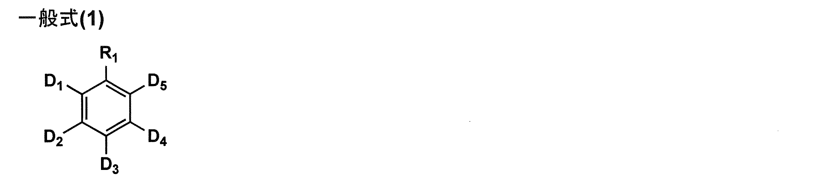
(式中、R1は、下記一般式(2)で表される構造を有する化合物の最低空軌道のエネルギー準位が-2.19eV以上となる基を表す。D1~D5は、それぞれ独立に、電子供与性の芳香族基を表し、D1~D5のうち、少なくとも1つはキラリティ発生部位を有する。なお、D1~D5は、それぞれ独立に、さらに置換基を有してもよい。)
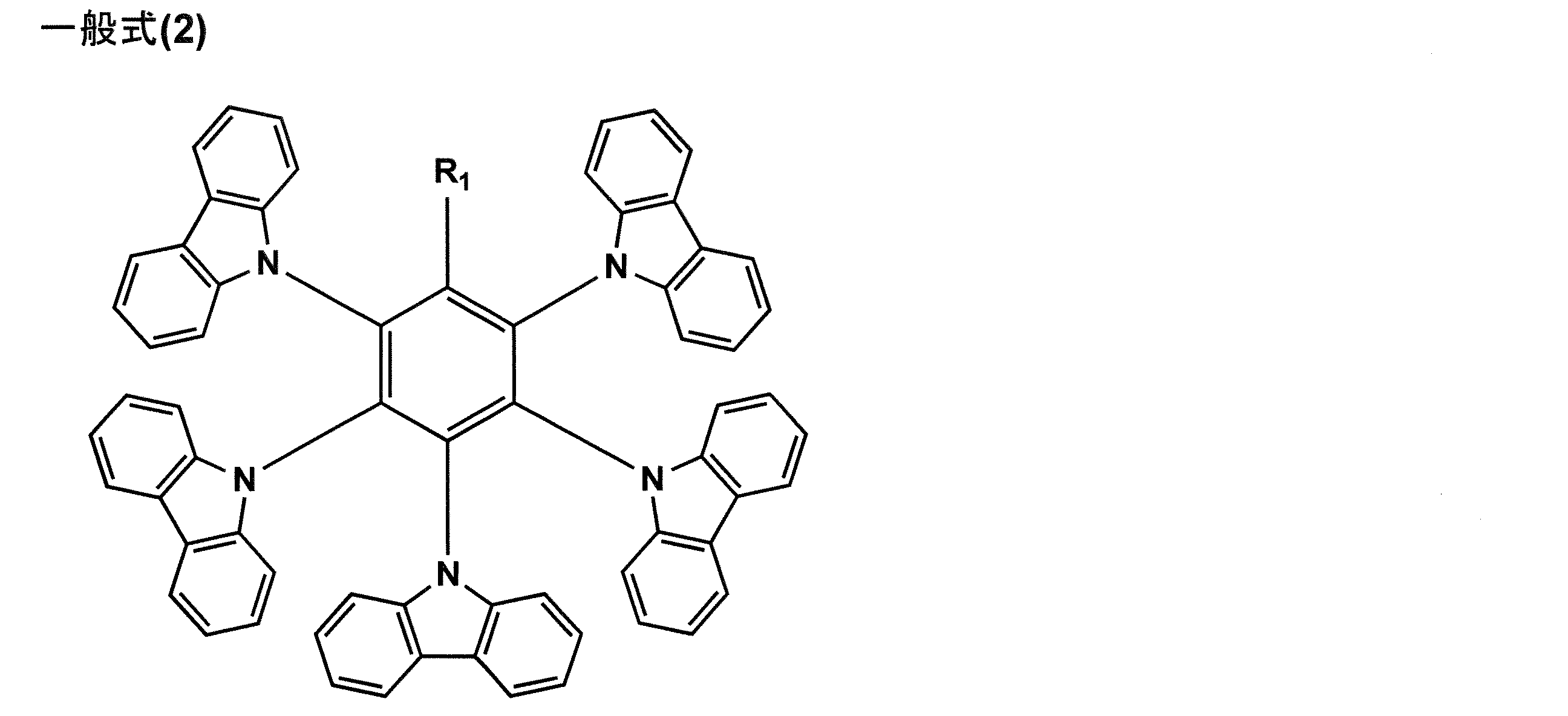
2.前記一般式(1)において、前記D1~D5のうち、少なくとも二つが、キラリティ発生部位を有することを特徴とする第1項に記載の電荷輸送性化合物。
3.前記一般式(1)において、前記D1~D5が、置換基を有していても良いカルバゾリル基又はカルボリニル基を表すことを特徴とする第1項又は第2項に記載の電荷輸送性化合物。
4.前記一般式(1)において、前記R1が、置換基を有していてもよい芳香族基であることを特徴とする第1項から第3項までのいずれか一項に記載の電荷輸送性化合物。
5.前記一般式(1)において、前記R1が、キラリティ発生部位を有することを特徴とする第1項から第4項までのいずれか一項に記載の電荷輸送性化合物。
6.第1項から第5項までのいずれか一項に記載の電荷輸送性化合物を製造する電荷輸送性化合物の製造方法であって、
求核置換反応により前記D1~D5をそれぞれ導入することを特徴とする電荷輸送性化合物の製造方法。
求核置換反応により前記D1~D5をそれぞれ導入することを特徴とする電荷輸送性化合物の製造方法。
7.第1項から第5項までのいずれか一項に記載の電荷輸送性化合物を含有することを特徴とするインク組成物。
8.第1項から第5項までのいずれか一項に記載の電荷輸送性化合物を含有することを特徴とする有機エレクトロルミネッセンス素子材料。
9.第1項から第5項までのいずれか一項に記載の電荷輸送性化合物を含有し、前記電荷輸送性化合物が蛍光を放射することを特徴とする発光材料。
10.前記蛍光が、遅延蛍光であることを特徴とする第9項に記載の発光材料。
11.第1項から第5項までのいずれか一項に記載の電荷輸送性化合物を含有することを特徴とする発光性薄膜。
12.陽極と、陰極と、前記陽極と前記陰極との間に設けられた発光層とを含み、前記発光層の少なくとも一層が、第1項から第5項までのいずれか一項に記載の電荷輸送性化合物を含有することを特徴とする有機エレクトロルミネッセンス素子。
本発明の上記手段により、電荷移動/発光性薄膜の通電経時での物性変動を抑制し、発光効率及び発光素子寿命に優れた電荷輸送性化合物及びその製造方法を提供することができる。さらに、前記電荷輸送性化合物を含有するインク組成物、有機エレクトロルミネッセンス素子材料、発光材料、発光性薄膜及び有機エレクトロルミネッセンス素子を提供することができる。
本発明の効果の発現機構又は作用機構については、明確にはなっていないが、以下のように推察している。
一般に、14π電子以上のπ電子を含む縮合含窒素芳香族化合物及びそのような化合物由来の芳香族環基を置換基として有する芳香族化合物は、芳香族性が炭化水素系置換基を有する芳香族化合物よりも強く、CH-π相互作用が強固に働くため、通電経時又は高温保存下では電荷移動/発光性薄膜の膜物性が変動して高密度化や凝集、結晶化が起こる。
一般に、14π電子以上のπ電子を含む縮合含窒素芳香族化合物及びそのような化合物由来の芳香族環基を置換基として有する芳香族化合物は、芳香族性が炭化水素系置換基を有する芳香族化合物よりも強く、CH-π相互作用が強固に働くため、通電経時又は高温保存下では電荷移動/発光性薄膜の膜物性が変動して高密度化や凝集、結晶化が起こる。
本発明の電荷輸送性化合物は、ベンゼン環上の5つの置換基のうちどれか一つでも非対称の化学構造を持つことで、アトロプ異性体の混合物となるため、そのエントロピー増大効果により、分子同士のエンタルピーに由来する分子間相互作用は抑制され、通電経時でも高温保存下でも、安定なアモルファス膜を形成することが可能となる。
加えて、従来のカルバゾリル基を有するベンゾニトリル誘導体に対して、ベンゼン環に置換する電子吸引性基をシアノ基から、弱アクセプターの置換基に変更することによって、最低空軌道(LUMO)のエネルギー準位をより高くすることができる。これによって発光中心が発光層と電子輸送層の界面近傍から発光層中の正孔輸送側に移動し、発光中心が集中することなく、より均一に発光することから、素子寿命を長くできるとともに良好な発光効率を実現できるものと推察される。さらに、弱アクセプターの置換基に変更することで、発光色もより短波長にすることができるものと推察される。
本発明の電荷輸送性化合物は、前記一般式(1)で表される構造を有し、最低励起一重項エネルギー準位と最低励起三重項エネルギー準位とのエネルギー差の絶対値ΔEstが、0.30eV以下であることを特徴とする。
この特徴は、下記各実施形態に共通又は対応する技術的特徴である。
本発明の実施態様としては、前記一般式(1)において、前記D1~D5のうち、少なくとも二つが、キラリティ発生部位を有することが、異性体の数の増加によるエントロピー増大効果として、電荷移動/発光性薄膜の安定性を高めることができる点で好ましい。なお、隣接する位置に5つ連続的に置換した芳香族基により立体的に遮蔽されるため、CH-π相互作用は分子間では起きにくくなるため、分子のスタッキングは抑制され、膜物性変動が低くなる点でも好ましい。
また、前記一般式(1)において、前記D1~D5が、置換基を有していても良いカルバゾリル基又はカルボリニル基を表すことが、電荷移動性を向上させる点で好ましい。
前記一般式(1)において、前記R1が、置換基を有していてもよい芳香族基であることが、化学安定性の観点から好ましい。
本発明の実施態様としては、前記一般式(1)において、前記D1~D5のうち、少なくとも二つが、キラリティ発生部位を有することが、異性体の数の増加によるエントロピー増大効果として、電荷移動/発光性薄膜の安定性を高めることができる点で好ましい。なお、隣接する位置に5つ連続的に置換した芳香族基により立体的に遮蔽されるため、CH-π相互作用は分子間では起きにくくなるため、分子のスタッキングは抑制され、膜物性変動が低くなる点でも好ましい。
また、前記一般式(1)において、前記D1~D5が、置換基を有していても良いカルバゾリル基又はカルボリニル基を表すことが、電荷移動性を向上させる点で好ましい。
前記一般式(1)において、前記R1が、置換基を有していてもよい芳香族基であることが、化学安定性の観点から好ましい。
前記一般式(1)において、前記R1が、キラリティ発生部位を有することが、異性体の数の増加によるエントロピー増大効果として、電荷移動/発光性薄膜の安定性を高めることができる点で好ましい。
本発明の電荷輸送性化合物の製造方法は、求核置換反応によりD1~D5をそれぞれ導入することを特徴とする。これにより、副生成物が少なく、収率良く製造することができる。
本発明の電荷輸送性化合物の製造方法は、求核置換反応によりD1~D5をそれぞれ導入することを特徴とする。これにより、副生成物が少なく、収率良く製造することができる。
本発明の電荷輸送性化合物は、インク組成物、有機エレクトロルミネッセンス素子材料、及び発光性薄膜に好適に用いられる。
本発明の電荷輸送性化合物は、発光材料に好適に用いられ、蛍光を放射し、前記蛍光が、遅延蛍光であることが好ましい。
本発明の有機エレクトロルミネッセンス素子は、陽極と、陰極と、前記陽極と前記陰極との間に設けられた発光層とを含み、前記発光層の少なくとも一層が、本発明の電荷輸送性化合物を含有することを特徴とする。これにより、発光効率の向上及び発光素子寿命の向上を図れ、かつ深い青色を発光する有機EL素子を提供することができる。
本発明の電荷輸送性化合物は、発光材料に好適に用いられ、蛍光を放射し、前記蛍光が、遅延蛍光であることが好ましい。
本発明の有機エレクトロルミネッセンス素子は、陽極と、陰極と、前記陽極と前記陰極との間に設けられた発光層とを含み、前記発光層の少なくとも一層が、本発明の電荷輸送性化合物を含有することを特徴とする。これにより、発光効率の向上及び発光素子寿命の向上を図れ、かつ深い青色を発光する有機EL素子を提供することができる。
以下、本発明とその構成要素及び本発明を実施するための形態・態様について説明をする。なお、本願において、「~」は、その前後に記載される数値を下限値及び上限値として含む意味で使用する。
[本発明の電荷輸送性化合物]
本発明の電荷輸送性化合物は、下記一般式(1)で表される構造を有し、最低励起一重項エネルギー準位と最低励起三重項エネルギー準位とのエネルギー差の絶対値ΔEstが、0.30eV以下であることを特徴とする。
本発明の電荷輸送性化合物は、下記一般式(1)で表される構造を有し、最低励起一重項エネルギー準位と最低励起三重項エネルギー準位とのエネルギー差の絶対値ΔEstが、0.30eV以下であることを特徴とする。
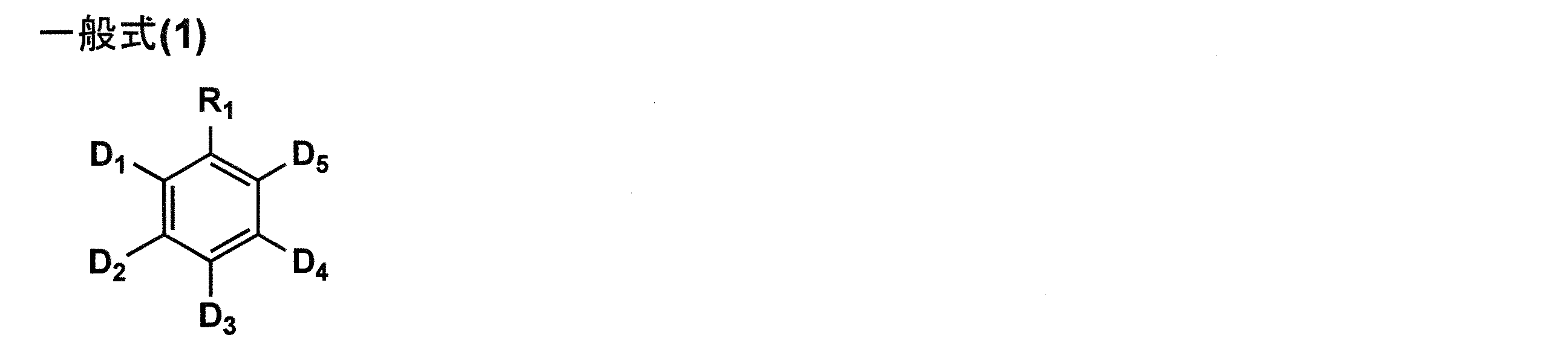
(式中、R1は、下記一般式(2)で表される構造を有する化合物の最低空軌道のエネルギー準位が-2.19eV以上となる基を表す。D1~D5は、それぞれ独立に、電子供与性の芳香族基を表し、D1~D5のうち、少なくとも1つはキラリティ発生部位を有する。なお、D1~D5は、それぞれ独立に、さらに置換基を有してもよい。)
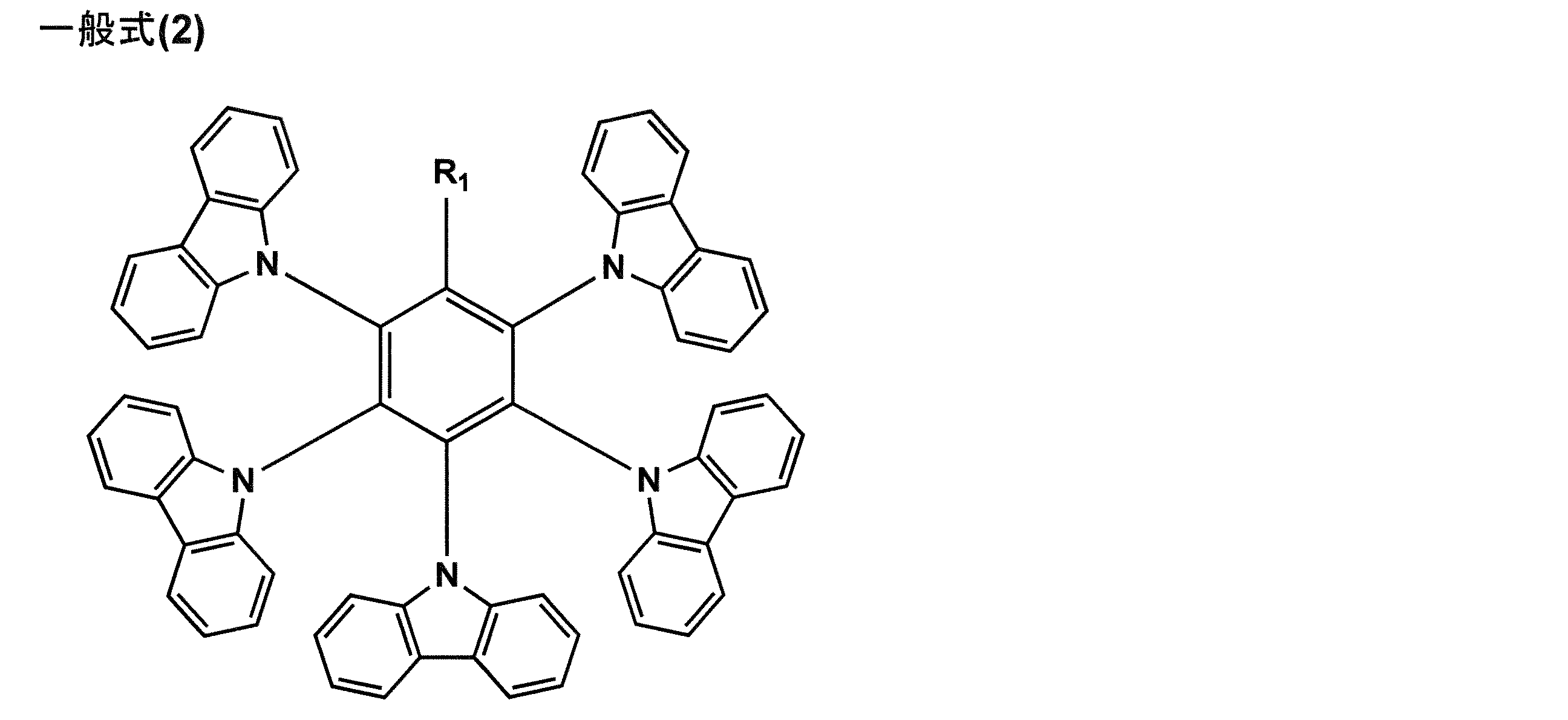
前記一般式(1)において、R1は、前記一般式(2)で表される構造を有する化合物の最低空軌道のエネルギー準位が-2.19eV以上となる基を表す。このようにベンゼン環に置換する電子吸引性基をシアノ基から、弱アクセプターの置換基に変更することによって、素子寿命を長くすることができ、かつ発光色もより短波長にすることができる。
R1は上記の計算で最低空軌道のエネルギー準位が-2.19eV以上となる基であれば特に制限はないが、置換基を有してもよい芳香族基であることが好ましい。芳香族基としては、芳香族炭化水素環基と芳香族複素環基が挙げられ、これらの中から上記エネルギー準位が-2.19eV以上となる基を選ぶことができる。
芳香族炭化水素環基としては、例えば、ベンゼン環、ビフェニル、ナフタレン環、アズレン環、アントラセン環、フェナントレン環、ピレン環、クリセン環、ナフタセン環、トリフェニレン環、o-ターフェニル環、m-ターフェニル環、p-ターフェニル環、アセナフテン環、コロネン環、インデン環、フルオレン環、フルオラントレン環、ナフタセン環、ペンタセン環、ペリレン環、ペンタフェン環、ピセン環、ピレン環、ピラントレン環、アンスラアントレン環、テトラリン等から導出される基等を挙げられる。
芳香族複素環基としては、例えば、フラン環、ジベンゾフラン環、チオフェン環、ジベンゾチオフェン環、オキサゾール環、ピロール環、ピリジン環、ピリダジン環、ピリミジン環、ピラジン環、トリアジン環、ベンゾイミダゾール環、オキサジアゾール環、トリアゾール環、イミダゾール環、ピラゾール環、チアゾール環、インドール環、インダゾール環、ベンゾイミダゾール環、ベンゾチアゾール環、ベンゾオキサゾール環、キノキサリン環、キナゾリン環、シンノリン環、キノリン環、イソキノリン環、フタラジン環、ナフチリジン環、カルバゾール環、カルボリン環、ジアザカルバゾール環(カルボリン環を構成する炭化水素環の炭素原子の一つがさらに窒素原子で置換されている環等から導出される基。)等を挙げることができる。
(キラリティ発生部位)
また、R1が、キラリティ発生部位を有することが好ましい。異性体の数の増加によるエントロピー増大効果として、電荷移動/発光性薄膜の安定性を高めることができる。
また、R1が、キラリティ発生部位を有することが好ましい。異性体の数の増加によるエントロピー増大効果として、電荷移動/発光性薄膜の安定性を高めることができる。
キラリティ発生部位を有するタイプとしては、オルト位に嵩高い置換基を持つビアリール基のような回転異性性を付与する結合軸(アトロプ異性軸)を有する分子、いわゆる軸不斉化合物であることが好ましい。
〔ΔEst〕
本発明の電荷輸送性化合物は、最低励起一重項エネルギー準位と最低励起三重項エネルギー準位とのエネルギー差の絶対値ΔEstが、0.30eV以下である。このような化合物は、分子内に重原子を持っていないにもかかわらず、ΔEstが小さいために通常では起こりえない三重項励起状態から一重項励起状態への逆項間交差が起こる。さらに、一重項励起状態から基底状態への失活(=蛍光発光)の速度定数が極めて大きいことから、三重項励起子はそれ自体が基底状態に熱的に失活(無輻射失活)するよりも、一重項励起状態経由で蛍光を発しながら基底状態に戻る方が速度論的に有利である。そのため、本発明の電荷輸送性化合物は発光材料として用いることができる。具体的には熱活性型遅延蛍光発光性(TADF)化合物として用いることができる。このようなTADF化合物では理想的には100%の蛍光発光が可能となる。
本発明の電荷輸送性化合物は、最低励起一重項エネルギー準位と最低励起三重項エネルギー準位とのエネルギー差の絶対値ΔEstが、0.30eV以下である。このような化合物は、分子内に重原子を持っていないにもかかわらず、ΔEstが小さいために通常では起こりえない三重項励起状態から一重項励起状態への逆項間交差が起こる。さらに、一重項励起状態から基底状態への失活(=蛍光発光)の速度定数が極めて大きいことから、三重項励起子はそれ自体が基底状態に熱的に失活(無輻射失活)するよりも、一重項励起状態経由で蛍光を発しながら基底状態に戻る方が速度論的に有利である。そのため、本発明の電荷輸送性化合物は発光材料として用いることができる。具体的には熱活性型遅延蛍光発光性(TADF)化合物として用いることができる。このようなTADF化合物では理想的には100%の蛍光発光が可能となる。
(ΔESTの算出)
本発明において、ΔESTは、分子軌道計算用ソフトウェアを用いて求める。
化合物の分子軌道計算による構造最適化及び電子密度分布の算出は、計算手法として、汎関数としてB3LYP、基底関数として6-31G(d)を用いた分子軌道計算用ソフトウェアを用いて算出することができる。分子軌道計算用ソフトウェアとして、米国Gaussian社製のGaussian09(Revision C.01,M.J.Frisch,et al,Gaussian,Inc.,2010.)を用いる。
本発明において、ΔESTは、分子軌道計算用ソフトウェアを用いて求める。
化合物の分子軌道計算による構造最適化及び電子密度分布の算出は、計算手法として、汎関数としてB3LYP、基底関数として6-31G(d)を用いた分子軌道計算用ソフトウェアを用いて算出することができる。分子軌道計算用ソフトウェアとして、米国Gaussian社製のGaussian09(Revision C.01,M.J.Frisch,et al,Gaussian,Inc.,2010.)を用いる。
この汎関数としてB3LYP、基底関数として6-31G(d)を用いた構造最適化計算から、さらに時間依存密度汎関数法(Time-Dependent DFT)による励起状態計算を実施してS1、T1のエネルギー準位(それぞれE(S1)、E(T1))を求めてΔEST=|E(S1)-E(T1)|として算出することができる。本発明においては、前述と同様の計算手法を用いて算出されたΔEstが0.3eV以下であり、好ましくは0.2eV以下である。
(最低空軌道のエネルギー準位の計算)
一般式(2)で表される構造を有する化合物の最低空軌道のエネルギー準位も、ΔEstの算出と同様に、汎関数としてB3LYP、基底関数として6-31G(d)を用いた分子軌道計算用ソフトウェア、米国Gaussian社製のGaussian09を用いて算出することができる。
一般式(2)で表される構造を有する化合物の最低空軌道のエネルギー準位も、ΔEstの算出と同様に、汎関数としてB3LYP、基底関数として6-31G(d)を用いた分子軌道計算用ソフトウェア、米国Gaussian社製のGaussian09を用いて算出することができる。
一般式(1)において、D1~D5は、それぞれ独立に、電子供与性の芳香族基を表し、
D1~D5のうち、少なくとも1つはキラリティ発生部位を有する。なお、D1~D5は、それぞれ独立に、さらに置換基を有してもよい。
前記一般式(1)において、前記D1~D5のうち、少なくとも二つが、キラリティ発生部位を有する構造を表すことが、異性体の数の増加によるエントロピー増大効果として、電荷移動/発光性薄膜の安定性を高めることができる点で好ましい。
D1~D5のうち、少なくとも1つはキラリティ発生部位を有する。なお、D1~D5は、それぞれ独立に、さらに置換基を有してもよい。
前記一般式(1)において、前記D1~D5のうち、少なくとも二つが、キラリティ発生部位を有する構造を表すことが、異性体の数の増加によるエントロピー増大効果として、電荷移動/発光性薄膜の安定性を高めることができる点で好ましい。
本発明に係る電子供与性で、キラリティ発生部位を有する構造としては、芳香族炭化水素誘導体、複素芳香族誘導体などの構造が好ましい。芳香族炭化水素誘導体としては、ベンゼン、ナフタレン、アントラセン、テトラセン、ペンタセン、クリセン、ヘリセンなどを挙げることができ、複素芳香族誘導体としては、フラン、チオフェン、ピロール、オキサゾール、チアゾール、イミダゾール、ベンゾフラン、ベンゾチオフェン、インドール、ジベンゾフラン、ジベンゾチオフェン、カルバゾール、ピリジン、ピラジン、ピリミジン、カルボリン等を挙げることができる。
また、前記一般式(1)において、前記D1~D5のうち、少なくとも一つが、下記一般式(3)で表される構造の置換基を有することが、電荷移動性を向上させる点で好ましい。
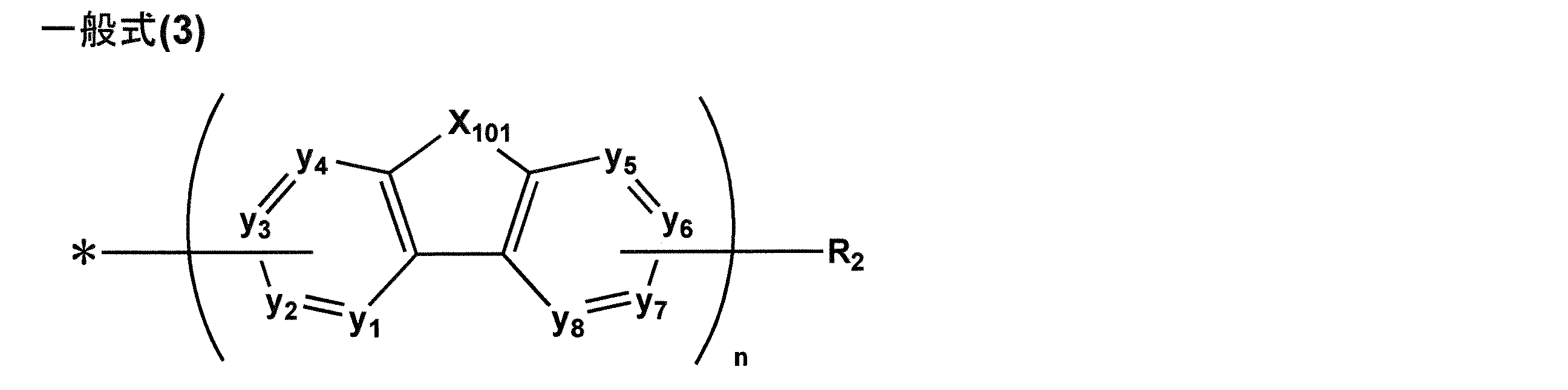
(式中、記号*は、前記一般式(1)中のD1~D5のいずれかへの結合位置を表す。X101は、NR101、酸素原子、硫黄原子、スルフィニル基、スルホニル基、CR102R103又はSiR104R105を表す。y1~y8は、それぞれ独立に、CR106又は窒素原子を表す。R101~R106は、それぞれ独立に、水素原子又は置換基を表し、互いに結合して環を形成してもよい。nは1~4の整数を表す。R2は置換基を表す。)
一般式(3)におけるR101~R106は、それぞれ独立に水素原子又は置換基を表し、ここにいう置換基は本発明に用いられる機能を阻害しない範囲で有してもよいものを指し、例えば、合成スキーム上置換基が導入されてしまう場合で、本発明の効果を奏する化合物は本発明に包含される旨を規定するものである。
一般式(3)におけるR101~R106は、それぞれ独立に水素原子又は置換基を表し、ここにいう置換基は本発明に用いられる機能を阻害しない範囲で有してもよいものを指し、例えば、合成スキーム上置換基が導入されてしまう場合で、本発明の効果を奏する化合物は本発明に包含される旨を規定するものである。
前記R101~R106でそれぞれ表される置換基としては、例えば、直鎖又は分岐アルキル基(例えば、メチル基、エチル基、プロピル基、イソプロピル基、t-ブチル基、ペンチル基、ヘキシル基、オクチル基、ドデシル基、トリデシル基、テトラデシル基、ペンタデシル基等)、アルケニル基(例えば、ビニル基、アリル基等)、アルキニル基(例えば、エチニル基、プロパルギル基等)、芳香族炭化水素環基(芳香族炭素環基、アリール基等ともいう。例えば、ベンゼン環、ビフェニル、ナフタレン環、アズレン環、アントラセン環、フェナントレン環、ピレン環、クリセン環、ナフタセン環、トリフェニレン環、o-ターフェニル環、m-ターフェニル環、p-ターフェニル環、アセナフテン環、コロネン環、インデン環、フルオレン環、フルオラントレン環、ナフタセン環、ペンタセン環、ペリレン環、ペンタフェン環、ピセン環、ピレン環、ピラントレン環、アンスラアントレン環、テトラリン等から導出される基)、芳香族複素環基(例えば、フラン環、ジベンゾフラン環、チオフェン環、ジベンゾチオフェン環、オキサゾール環、ピロール環、ピリジン環、ピリダジン環、ピリミジン環、ピラジン環、トリアジン環、ベンゾイミダゾール環、オキサジアゾール環、トリアゾール環、イミダゾール環、ピラゾール環、チアゾール環、インドール環、インダゾール環、ベンゾイミダゾール環、ベンゾチアゾール環、ベンゾオキサゾール環、キノキサリン環、キナゾリン環、シンノリン環、キノリン環、イソキノリン環、フタラジン環、ナフチリジン環、カルバゾール環、カルボリン環、ジアザカルバゾール環(カルボリン環を構成する炭化水素環の炭素原子の一つがさらに窒素原子で置換されている環等から導出される基。)、非芳香族炭化水素環基(例えば、シクロペンチル基、シクロヘキシル基等)、非芳香族複素環基(例えば、ピロリジル基、イミダゾリジル基、モルホリル基、オキサゾリジル基等)、アルコキシ基(例えば、メトキシ基、エトキシ基、プロピルオキシ基、ペンチルオキシ基、ヘキシルオキシ基、オクチルオキシ基、ドデシルオキシ基等)、シクロアルコキシ基(例えば、シクロペンチルオキシ基、シクロヘキシルオキシ基等)、アリールオキシ基(例えば、フェノキシ基、ナフチルオキシ基等)、アルキルチオ基(例えば、メチルチオ基、エチルチオ基、プロピルチオ基、ペンチルチオ基、ヘキシルチオ基、オクチルチオ基、ドデシルチオ基等)、シクロアルキルチオ基(例えば、シクロペンチルチオ基、シクロヘキシルチオ基等)、アリールチオ基(例えば、フェニルチオ基、ナフチルチオ基等)、アルコキシカルボニル基(例えば、メチルオキシカルボニル基、エチルオキシカルボニル基、ブチルオキシカルボニル基、オクチルオキシカルボニル基、ドデシルオキシカルボニル基等)、アリールオキシカルボニル基(例えば、フェニルオキシカルボニル基、ナフチルオキシカルボニル基等)、スルファモイル基(例えば、アミノスルホニル基、メチルアミノスルホニル基、ジメチルアミノスルホニル基、ブチルアミノスルホニル基、ヘキシルアミノスルホニル基、シクロヘキシルアミノスルホニル基、オクチルアミノスルホニル基、ドデシルアミノスルホニル基、フェニルアミノスルホニル基、ナフチルアミノスルホニル基、2-ピリジルアミノスルホニル基等)、アシル基(例えば、アセチル基、エチルカルボニル基、プロピルカルボニル基、ペンチルカルボニル基、シクロヘキシルカルボニル基、オクチルカルボニル基、2-エチルヘキシルカルボニル基、ドデシルカルボニル基、フェニルカルボニル基、ナフチルカルボニル基、ピリジルカルボニル基等)、アシルオキシ基(例えば、アセチルオキシ基、エチルカルボニルオキシ基、ブチルカルボニルオキシ基、オクチルカルボニルオキシ基、ドデシルカルボニルオキシ基、フェニルカルボニルオキシ基等)、アミド基(例えば、メチルカルボニルアミノ基、エチルカルボニルアミノ基、ジメチルカルボニルアミノ基、プロピルカルボニルアミノ基、ペンチルカルボニルアミノ基、シクロヘキシルカルボニルアミノ基、2-エチルヘキシルカルボニルアミノ基、オクチルカルボニルアミノ基、ドデシルカルボニルアミノ基、フェニルカルボニルアミノ基、ナフチルカルボニルアミノ基等)、カルバモイル基(例えば、アミノカルボニル基、メチルアミノカルボニル基、ジメチルアミノカルボニル基、プロピルアミノカルボニル基、ペンチルアミノカルボニル基、シクロヘキシルアミノカルボニル基、オクチルアミノカルボニル基、2-エチルヘキシルアミノカルボニル基、ドデシルアミノカルボニル基、フェニルアミノカルボニル基、ナフチルアミノカルボニル基、2-ピリジルアミノカルボニル基等)、ウレイド基(例えば、メチルウレイド基、エチルウレイド基、ペンチルウレイド基、シクロヘキシルウレイド基、オクチルウレイド基、ドデシルウレイド基、フェニルウレイド基ナフチルウレイド基、2-ピリジルアミノウレイド基等)、スルフィニル基(例えば、メチルスルフィニル基、エチルスルフィニル基、ブチルスルフィニル基、シクロヘキシルスルフィニル基、2-エチルヘキシルスルフィニル基、ドデシルスルフィニル基、フェニルスルフィニル基、ナフチルスルフィニル基、2-ピリジルスルフィニル基等)、アルキルスルホニル基(例えば、メチルスルホニル基、エチルスルホニル基、ブチルスルホニル基、シクロヘキシルスルホニル基、2-エチルヘキシルスルホニル基、ドデシルスルホニル基等)、アリールスルホニル基又はヘテロアリールスルホニル基(例えば、フェニルスルホニル基、ナフチルスルホニル基、2-ピリジルスルホニル基等)、アミノ基(例えば、アミノ基、エチルアミノ基、ジメチルアミノ基、ブチルアミノ基、シクロペンチルアミノ基、2-エチルヘキシルアミノ基、ドデシルアミノ基、アニリノ基、ナフチルアミノ基、2-ピリジルアミノ基等)、ハロゲン原子(例えば、フッ素原子、塩素原子、臭素原子等)、フッ化炭化水素基(例えば、フルオロメチル基、トリフルオロメチル基、ペンタフルオロエチル基、ペンタフルオロフェニル基等)、シアノ基、ニトロ基、ヒドロキシ基、チオール基、シリル基(例えば、トリメチルシリル基、トリイソプロピルシリル基、トリフェニルシリル基、フェニルジエチルシリル基等)、重水素原子等が挙げられる。
これらの置換基は、上記の置換基によってさらに置換されていてもよい。また、これらの置換基は複数が互いに結合して環を形成していてもよい。
一般式(3)で表される構造の中でも、X101が、NR101、酸素原子又は硫黄原子である化合物が好ましい。より好ましくは、X101及びy1~y8とともに形成される基が、カルバゾリル基又はカルボリニル基を表すことが、電荷移動性を向上させる点から好ましい。
一般式(3)におけるnは1~4の整数を表し、好ましくは1~2である。
一般式(3)におけるnは1~4の整数を表し、好ましくは1~2である。
また、一般式(3)におけるR2は前記R101~R106と同様に置換基を表すが、溶解性を向上させる置換基が好ましい。当該置換基としては、例えば、直鎖又は分岐アルキル基(例えば、メチル基、エチル基、プロピル基、イソプロピル基、t-ブチル基、ペンチル基、ヘキシル基、オクチル基、ドデシル基、トリデシル基、テトラデシル基、ペンタデシル基等)、芳香族炭化水素環基(芳香族炭素環基、アリール基等ともいう。例えば、ベンゼン環、ビフェニル、ナフタレン環、アズレン環、アントラセン環、フェナントレン環、ピレン環、クリセン環、ナフタセン環、トリフェニレン環、o-ターフェニル環、m-ターフェニル環、p-ターフェニル環、アセナフテン環、コロネン環、インデン環、フルオレン環、フルオラントレン環、ナフタセン環、ペンタセン環、ペリレン環、ペンタフェン環、ピセン環、ピレン環、ピラントレン環、アンスラアントレン環、テトラリン等から導出される基)、芳香族複素環基(例えば、フラン環、ジベンゾフラン環、チオフェン環、ジベンゾチオフェン環、オキサゾール環、ピロール環、ピリジン環、ピリダジン環、ピリミジン環、ピラジン環、トリアジン環、ベンゾイミダゾール環、オキサジアゾール環、トリアゾール環、イミダゾール環、ピラゾール環、チアゾール環、インドール環、インダゾール環、ベンゾイミダゾール環、ベンゾチアゾール環、ベンゾオキサゾール環、キノキサリン環、キナゾリン環、シンノリン環、キノリン環、イソキノリン環、フタラジン環、ナフチリジン環、カルバゾール環、カルボリン環、ジアザカルバゾール環(カルボリン環を構成する炭化水素環の炭素原子の一つがさらに窒素原子で置換されている環等から導出される基。)、非芳香族炭化水素環基(例えば、シクロペンチル基、シクロヘキシル基等)、非芳香族複素環基(例えば、ピロリジル基、イミダゾリジル基、モルホリル基、オキサゾリジル基等)等が挙げられる。
前記一般式(1)で表される構造を有する電荷輸送性化合物の例示化合物を以下に示すが、これに限定されるものではない。


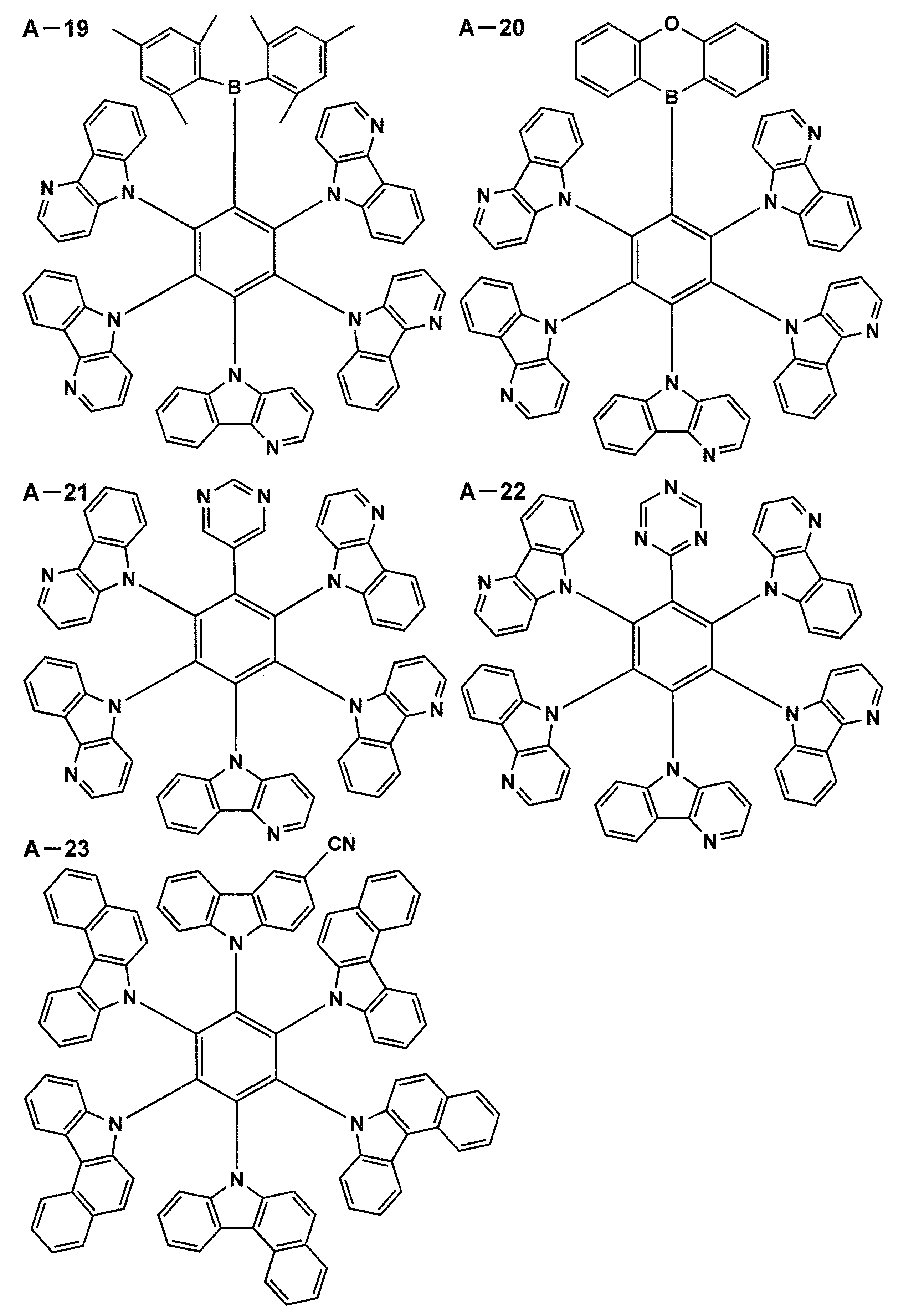

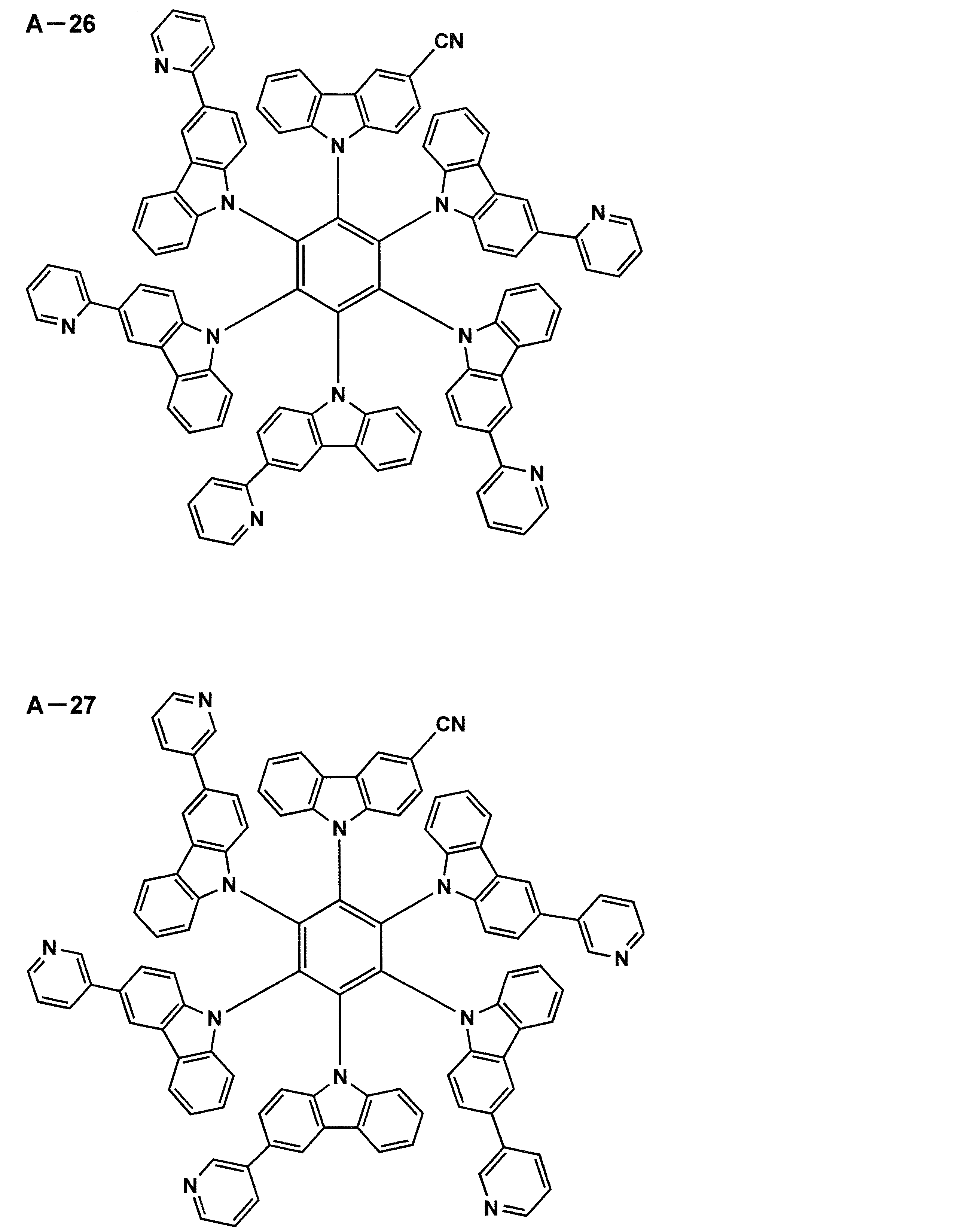

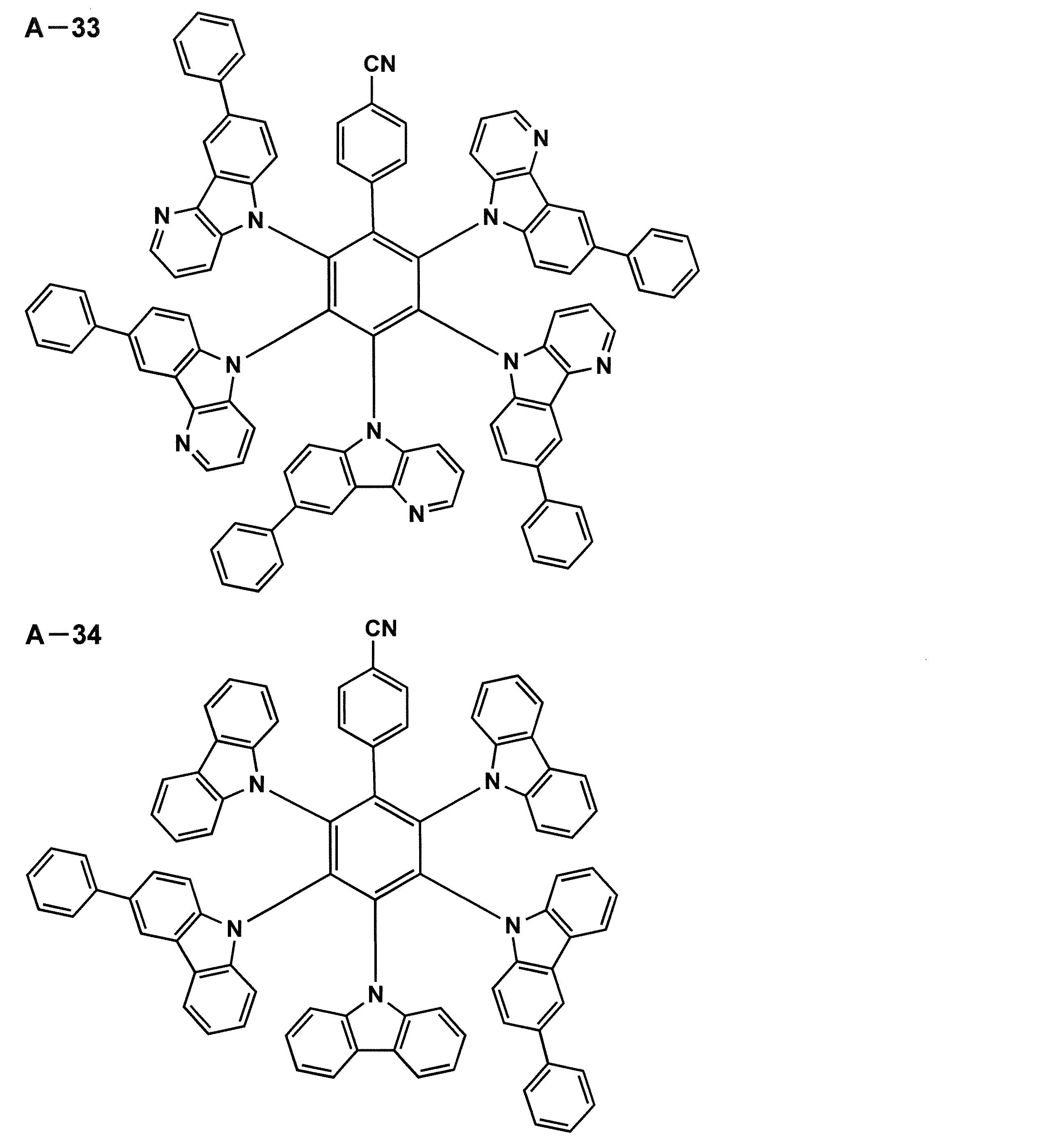

[電荷輸送性化合物の製造方法]
本発明の電荷輸送性化合物の製造方法は、求核置換反応により前記置換基D1~D5をそれぞれ導入することを特徴とする。
本発明の電荷輸送性化合物の製造方法は、求核置換反応により前記置換基D1~D5をそれぞれ導入することを特徴とする。
具体的には、2,3,4,5,6-ペンタフルオロベンゾ体を溶媒(テトラヒドロフラン(THF)、ジメチルホルムアミド(DMF)、N-メチル-2-ピロリドン(NMP)等)に溶解させ、強塩基(炭酸カリウム、炭酸セシウム、水素化ナトリウム、水素化カリウム等)存在下で、置換基を有していてもよいカルバゾールやカルボリン等を反応させることで製造することができる。
[有機EL素子]
本発明の有機EL素子は、少なくとも、一対の電極と一つ又は複数の発光層とを有する有機エレクトロルミネッセンス素子であって、前記発光層の少なくとも一層が、本発明の電荷輸送性化合物を含有することを特徴とする。
本発明の有機EL素子は、少なくとも、一対の電極と一つ又は複数の発光層とを有する有機エレクトロルミネッセンス素子であって、前記発光層の少なくとも一層が、本発明の電荷輸送性化合物を含有することを特徴とする。
本発明の有機EL素子における代表的な素子構成としては、以下の構成を挙げることができるが、これらに限定されるものではない。
(i)陽極/発光層/陰極
(ii)陽極/発光層/電子輸送層/陰極
(iii)陽極/正孔輸送層/発光層/陰極
(iv)陽極/正孔輸送層/発光層/電子輸送層/陰極
(v)陽極/正孔輸送層/発光層/電子輸送層/電子注入層/陰極
(vi)陽極/正孔注入層/正孔輸送層/発光層/電子輸送層/陰極
(vii)陽極/正孔注入層/正孔輸送層/(電子阻止層/)発光層/(正孔阻止層/)電子輸送層/電子注入層/陰極
上記の中で(vii)の構成が好ましく用いられるが、これに限定されるものではない。
(i)陽極/発光層/陰極
(ii)陽極/発光層/電子輸送層/陰極
(iii)陽極/正孔輸送層/発光層/陰極
(iv)陽極/正孔輸送層/発光層/電子輸送層/陰極
(v)陽極/正孔輸送層/発光層/電子輸送層/電子注入層/陰極
(vi)陽極/正孔注入層/正孔輸送層/発光層/電子輸送層/陰極
(vii)陽極/正孔注入層/正孔輸送層/(電子阻止層/)発光層/(正孔阻止層/)電子輸送層/電子注入層/陰極
上記の中で(vii)の構成が好ましく用いられるが、これに限定されるものではない。
本発明に係る発光層は、単層又は複数層で構成されており、発光層が複数の場合は各発光層の間に非発光性の中間層を設けてもよい。必要に応じて、発光層と陰極との間に正孔阻止層(正孔障壁層ともいう)や電子注入層(陰極バッファー層ともいう)を設けてもよく、また、発光層と陽極との間に電子阻止層(電子障壁層ともいう)や正孔注入層(陽極バッファー層ともいう)を設けてもよい。
本発明に係る電子輸送層とは、電子を輸送する機能を有する層であり、広い意味で電子注入層、正孔阻止層も電子輸送層に含まれる。また、複数層で構成されていてもよい。
本発明に係る正孔輸送層とは、正孔を輸送する機能を有する層であり、広い意味で正孔注入層、電子阻止層も正孔輸送層に含まれる。また、複数層で構成されていてもよい。
上記の代表的な素子構成において、陽極と陰極を除いた層を「有機層」ともいう。
本発明に係る正孔輸送層とは、正孔を輸送する機能を有する層であり、広い意味で正孔注入層、電子阻止層も正孔輸送層に含まれる。また、複数層で構成されていてもよい。
上記の代表的な素子構成において、陽極と陰極を除いた層を「有機層」ともいう。
(タンデム構造)
本発明の有機EL素子は、少なくとも1層の発光層を含む発光ユニットを複数積層した、いわゆるタンデム構造の素子であってもよい。
タンデム構造の代表的な素子構成としては、例えば以下の構成を挙げることができる。
本発明の有機EL素子は、少なくとも1層の発光層を含む発光ユニットを複数積層した、いわゆるタンデム構造の素子であってもよい。
タンデム構造の代表的な素子構成としては、例えば以下の構成を挙げることができる。
陽極/第1発光ユニット/第2発光ユニット/第3発光ユニット/陰極
陽極/第1発光ユニット/中間層/第2発光ユニット/中間層/第3発光ユニット/陰極
陽極/第1発光ユニット/中間層/第2発光ユニット/中間層/第3発光ユニット/陰極
ここで、上記第1発光ユニット、第2発光ユニット及び第3発光ユニットは全て同じであっても、異なっていてもよい。また二つの発光ユニットが同じであり、残る一つが異なっていてもよい。
また、第3発光ユニットはなくてもよく、一方で第3発光ユニットと電極の間にさらに発光ユニットや中間層を設けてもよい。
また、第3発光ユニットはなくてもよく、一方で第3発光ユニットと電極の間にさらに発光ユニットや中間層を設けてもよい。
複数の発光ユニットは直接積層されていても、中間層を介して積層されていてもよく、中間層は、一般的に中間電極、中間導電層、電荷発生層、電子引抜層、接続層、中間絶縁層とも呼ばれ、陽極側の隣接層に電子を、陰極側の隣接層に正孔を供給する機能を持った層であれば、公知の材料及び構成を用いることができる。
中間層に用いられる材料としては、例えば、ITO(インジウム・スズ酸化物)、IZO(インジウム・亜鉛酸化物)、ZnO2、TiN、ZrN、HfN、TiOx、VOx、CuI、InN、GaN、CuAlO2、CuGaO2、SrCu2O2、LaB6、RuO2、Al等の導電性無機化合物層や、Au/Bi2O3等の2層膜や、SnO2/Ag/SnO2、ZnO/Ag/ZnO、Bi2O3/Au/Bi2O3、TiO2/TiN/TiO2、TiO2/ZrN/TiO2等の多層膜、またC60等のフラーレン類、オリゴチオフェン等の導電性有機物層、金属フタロシアニン類、無金属フタロシアニン類、金属ポルフィリン類、無金属ポルフィリン類等の導電性有機化合物層等が挙げられるが、本発明はこれらに限定されない。
発光ユニット内の好ましい構成としては、例えば上記の代表的な素子構成で挙げた(i)~(vii)の構成から、陽極と陰極を除いたもの等が挙げられるが、本発明はこれらに
限定されない。
限定されない。
タンデム型有機EL素子の具体例としては、例えば、米国特許第6337492号、米国特許第7420203号、米国特許第7473923号、米国特許第6872472号、米国特許第6107734号、米国特許第6337492号、国際公開第2005/009087号、特開2006-228712号公報、特開2006-24791号公報、特開2006-49393号公報、特開2006-49394号公報、特開2006-49396号公報、特開2011-96679号公報、特開2005-340187号公報、特許第4711424号、特許第3496681号、特許第3884564号、特許第4213169号、特開2010-192719号公報、特開2009-076929号公報、特開2008-078414号公報、特開2007-059848号公報、特開2003-272860号公報、特開2003-045676号公報、国際公開第2005/094130号等に記載の素子構成や構成材料等が挙げられるが、本発明はこれらに限定されない。
以下、本発明の有機EL素子を構成する各層について説明する。
以下、本発明の有機EL素子を構成する各層について説明する。
<発光層>
本発明に係る発光層は、電極又は隣接層から注入されてくる電子及び正孔が再結合し、励起子を経由して発光する場を提供する層であり、発光する部分は発光層の層内であっても、発光層と隣接層との界面であってもよい。
本発明に係る発光層は、電極又は隣接層から注入されてくる電子及び正孔が再結合し、励起子を経由して発光する場を提供する層であり、発光する部分は発光層の層内であっても、発光層と隣接層との界面であってもよい。
発光層の厚さの総和は、特に制限はないが、形成する層の均質性や、発光時に不必要な高電圧を印加するのを防止し、かつ、駆動電流に対する発光色の安定性向上の観点から、2nm~5μmの範囲内に調整することが好ましく、より好ましくは2~500nmの範囲内に調整され、さらに好ましくは5~200nmの範囲内に調整される。
また、個々の発光層の厚さとしては、2nm~1μmの範囲内に調整することが好ましく、より好ましくは2~200nmの範囲内に調整され、さらに好ましくは3~150nmの範囲に調整される。
発光層には、発光ドーパント(発光性ドーパント化合物、ドーパント化合物、単にドーパントともいう。)と、ホスト化合物(マトリックス材料、発光ホスト化合物、単にホストともいう。)と、を含有することが好ましい。
(1)発光ドーパント
発光ドーパントとしては、蛍光発光性ドーパント(蛍光ドーパント、蛍光性化合物ともいう。)と、遅延蛍光性ドーパント、リン光発光性ドーパント(リン光ドーパント、リン光性化合物ともいう。)が好ましく用いられる。本発明においては、少なくとも1層の発光層が、本発明の電荷輸送性化合物を含有することが好ましい。
発光ドーパントとしては、蛍光発光性ドーパント(蛍光ドーパント、蛍光性化合物ともいう。)と、遅延蛍光性ドーパント、リン光発光性ドーパント(リン光ドーパント、リン光性化合物ともいう。)が好ましく用いられる。本発明においては、少なくとも1層の発光層が、本発明の電荷輸送性化合物を含有することが好ましい。
本発明においては、発光層が発光ドーパントを5~40質量%の範囲内で含有することが好ましく、10~30質量%の範囲内で含有することがより好ましい。
発光層中の発光ドーパントの濃度については、使用される特定の発光ドーパント及びデバイスの必要条件に基づいて、任意に決定することができ、発光層の厚さ方向に対し、均一な濃度で含有されていてもよく、また任意の濃度分布を有していてもよい。
また、発光ドーパントは、複数種を併用して用いてもよく、構造の異なる発光ドーパント同士の組み合わせや、本発明のπ共役系化合物や、蛍光発光性化合物とリン光発光性化合物とを組み合わせて用いてもよい。これにより、任意の発光色を得ることができる。
本発明に係る有機EL素子の発光する色は、「新編色彩科学ハンドブック」(日本色彩学会編、東京大学出版会、1985)の108頁の図4.16において、分光放射輝度計CS-1000(コニカミノルタ(株)製)で測定した結果をCIE色度座標に当てはめたときの色で決定される。
本発明においては、1層又は複数層の発光層が、発光色の異なる複数の発光ドーパントを含有し、白色発光を示すことも好ましい。
白色を示す発光ドーパントの組み合わせについては特に限定はないが、例えば青と橙や、青と緑と赤の組み合わせ等が挙げられる。
白色を示す発光ドーパントの組み合わせについては特に限定はないが、例えば青と橙や、青と緑と赤の組み合わせ等が挙げられる。
本発明に係る有機EL素子における白色とは、特に限定はなく、橙色寄りの白色であっても青色寄りの白色であってもよいが、2度視野角正面輝度を前述の方法により測定した際に、1000cd/m2でのCIE1931表色系における色度がx=0.39±0.09、y=0.38±0.08の領域内にあることが好ましい。
(1.1)リン光発光性ドーパント
本発明に係るリン光発光性ドーパント(以下、「リン光ドーパント」ともいう。)について説明する。
本発明に係るリン光発光性ドーパント(以下、「リン光ドーパント」ともいう。)について説明する。
本発明に係るリン光ドーパントは、励起三重項からの発光が観測される化合物であり、具体的には、室温(25℃)にてリン光発光する化合物であり、リン光量子収率が、25℃において0.01以上の化合物であると定義されるが、好ましいリン光量子収率は0.1以上である。
上記リン光量子収率は、第4版実験化学講座7の分光IIの398頁(1992年版、丸善)に記載の方法により測定できる。溶液中でのリン光量子収率は種々の溶媒を用いて測定できるが、本発明に係るリン光ドーパントは、任意の溶媒のいずれかにおいて上記リン光量子収率(0.01以上)が達成されればよい。
リン光ドーパントの発光は原理としては2種挙げられ、一つはキャリアが輸送されるホスト化合物上でキャリアの再結合が起こってホスト化合物の励起状態が生成し、このエネルギーをリン光ドーパントに移動させることでリン光ドーパントからの発光を得るというエネルギー移動型である。もう一つはリン光ドーパントがキャリアトラップとなり、リン光ドーパント上でキャリアの再結合が起こりリン光ドーパントからの発光が得られるというキャリアトラップ型である。いずれの場合においても、リン光ドーパントの励起状態のエネルギーはホスト化合物の励起状態のエネルギーよりも低いことが条件である。
本発明において使用できるリン光ドーパントとしては、有機EL素子の発光層に使用される公知のものの中から適宜選択して用いることができる。
本発明に使用できる公知のリン光ドーパントの具体例としては、以下の文献に記載されている化合物等が挙げられる。
本発明に使用できる公知のリン光ドーパントの具体例としては、以下の文献に記載されている化合物等が挙げられる。
Nature 395,151(1998)、Appl.Phys.Lett.78,1622(2001)、Adv.Mater.19,739(2007)、Chem.Mater.17,3532(2005)、Adv.Mater.17,1059(2005)、国際公開第2009/100991号、国際公開第2008/101842号、国際公開第2003/040257号、米国特許公開第2006/835469号、米国特許公開第2006/0202194号、米国特許公開第2007/0087321号、米国特許公開第2005/0244673号、Inorg.Chem.40,1704(2001)、Chem.Mater.16,2480(2004)、Adv.Mater.16,2003(2004)、Angew.Chem.Int.Ed.2006,45,7800、Appl.Phys.Lett.86,153505(2005)、Chem.Lett.34,592(2005)、Chem.Commun.2906(2005)、Inorg.Chem.42,1248(2003)、国際公開第2009/050290号、国際公開第2002/015645号、国際公開第2009/000673号、米国特許公開第2002/0034656号、米国特許第7332232号、米国特許公開第2009/0108737号、米国特許公開第2009/0039776号、米国特許第6921915号、米国特許第6687266号、米国特許公開第2007/0190359号、米国特許公開第2006/0008670号、米国特許公開第2009/0165846号、米国特許公開第2008/0015355号、米国特許第7250226号、米国特許第7396598号、米国特許公開第2006/0263635号、米国特許公開第2003/0138657号、米国特許公開第2003/0152802号、米国特許第7090928号、Angew.Chem.Int.Ed.47,1(2008)、Chem.Mater.18,5119(2006)、Inorg.Chem.46,4308(2007)、Organometallics 23,3745(2004)、Appl.Phys.Lett.74,1361(1999)、国際公開第2002/002714号、国際公開第2006/009024号、国際公開第2006/056418号、国際公開第2005/019373号、国際公開第2005/123873号、国際公開第2007/004380号、国際公開第2006/082742号、米国特許公開第2006/0251923号、米国特許公開第2005/0260441号、米国特許第7393599号、米国特許第7534505号、米国特許第7445855号、米国特許公開第2007/0190359号、米国特許公開第2008/0297033号、米国特許第7338722号、米国特許公開第2002/0134984号、米国特許第7279704号、米国特許公開第2006/098120号、米国特許公開第2006/103874号、国際公開第2005/076380号、国際公開第2010/032663号、国際公開第2008/140115号、国際公開第2007/052431号、国際公開第2011/134013号、国際公開第2011/157339号、国際公開第2010/086089号、国際公開第2009/113646号、国際公開第2012/020327号、国際公開第2011/051404号、国際公開第2011/004639号、国際公開第2011/073149号、米国特許公開第2012/228583号、米国特許公開第2012/212126号、特開2012-069737号公報、特開2012-195554号公報、特開2009-114086号公報、特開2003-81988号公報、特開2002-302671号公報、特開2002-363552号公報等である。
中でも、好ましいリン光ドーパントとしてはIrを中心金属に有する有機金属錯体が挙げられる。さらに好ましくは、金属-炭素結合、金属-窒素結合、金属-酸素結合、金属-硫黄結合の少なくとも一つの配位様式を含む錯体が好ましい。
(1.2)蛍光発光性ドーパント
本発明に係る蛍光発光性ドーパント(以下、「蛍光ドーパント」ともいう。)について説明する。
本発明に係る蛍光発光性ドーパント(以下、「蛍光ドーパント」ともいう。)について説明する。
本発明に係る蛍光ドーパントは、励起一重項からの発光が可能な化合物であり、励起一重項からの発光が観測される限り特に限定されない。
本発明に係る蛍光ドーパントは、本発明の電荷輸送性化合物を用いてもよいし、有機EL素子の発光層に使用される公知の蛍光ドーパントや他の遅延蛍光性ドーパントの中から適宜選択して用いてもよい。
本発明に係る蛍光ドーパントとしては、例えば、アントラセン誘導体、ピレン誘導体、クリセン誘導体、フルオランテン誘導体、ペリレン誘導体、フルオレン誘導体、アリールアセチレン誘導体、スチリルアリーレン誘導体、スチリルアミン誘導体、アリールアミン誘導体、ホウ素錯体、クマリン誘導体、ピラン誘導体、シアニン誘導体、クロコニウム誘導体、スクアリウム誘導体、オキソベンツアントラセン誘導体、フルオレセイン誘導体、ローダミン誘導体、ピリリウム誘導体、ペリレン誘導体、ポリチオフェン誘導体、又は希土類錯体系化合物等が挙げられる。
遅延蛍光性ドーパントの具体例としては、例えば、国際公開第2011/156793号、特開2011-213643号公報、特開2010-93181号公報等に記載の化合物が挙げられるが、本発明はこれらに限定されない。
(2)ホスト化合物
本発明に係るホスト化合物は、発光層において主に電荷の注入及び輸送を担う化合物であり、有機EL素子においてそれ自体の発光は実質的に観測されない。
本発明に係るホスト化合物は、発光層において主に電荷の注入及び輸送を担う化合物であり、有機EL素子においてそれ自体の発光は実質的に観測されない。
好ましくは室温(25℃)においてリン光発光のリン光量子収率が、0.1未満の化合物であり、さらに好ましくはリン光量子収率が0.01未満の化合物である。また、発光層に含有される化合物の内で、その層中での質量比が20%以上であることが好ましい。
また、ホスト化合物の励起状態エネルギーは、同一層内に含有される発光ドーパントの励起状態エネルギーよりも高いことが好ましい。
ホスト化合物は、単独で用いてもよく、又は複数種併用して用いてもよい。ホスト化合物を複数種用いることで、電荷の移動を調整することが可能であり、有機EL素子を高効率化することができる。
ホスト化合物としては、本発明の電荷輸送性化合物を用いてもよく、特に制限はなく、従来有機EL素子で用いられる化合物を用いることができる。低分子化合物でも繰り返し単位を有する高分子化合物でもよく、また、ビニル基やエポキシ基のような反応性基を有する化合物でもよい。
逆エネルギー移動の観点から、ドーパントの励起一重項エネルギー準位より高い励起エネルギーをもつものが好ましく、さらにドーパントの励起三重項エネルギー準位より高い励起三重項エネルギーをもつものがより好ましい。
ホスト化合物は、発光層内においてキャリアの輸送及び励起子の生成を担う。そのため、カチオンラジカル状態、アニオンラジカル状態、及び励起状態の全ての活性種の状態において安定に存在でき、分解や付加反応などの化学変化を起こさないこと、さらに、層中において通電経時でホスト分子がオングストロームレベルで移動しないことが好ましい。
また、特に併用する発光ドーパントがTADF発光を示す場合には、TADF化合物の励起三重項状態の存在時間が長いことから、ホスト化合物自体のT1エネルギー準位が高いこと、さらにホスト化合物同士が会合した状態で低T1状態を作らないこと、TADF化合物とホスト化合物とがエキサイプレックスを形成しないこと、ホスト化合物が電界によりエレクトロマーを形成しないことなど、ホスト化合物が低T1化しないような分子構造の適切な設計が必要となる。
このような要件を満たすためには、ホスト化合物自体が電子のホッピング移動性が高いこと、かつ、正孔のホッピング移動が高いこと、励起三重項状態となったときの構造変化が小さいことが必要である。このような要件を満たすホスト化合物の代表格としてカルバゾール骨格、アザカルバゾール骨格、ジベンゾフラン骨格、ジベンゾチオフェン骨格又はアザジベンゾフラン骨格などの、高T1エネルギー準位を有するものが好ましく挙げられる。
公知のホスト化合物としては、正孔輸送能又は電子輸送能を有しつつ、かつ、発光の長波長化を防ぎ、さらに、有機EL素子を高温駆動時や素子駆動中の発熱に対して安定して動作させる観点から、高いガラス転移温度(Tg)を有することが好ましい。好ましくはTgが90℃以上であり、より好ましくは120℃以上である。
ここで、ガラス転移点(Tg)とは、DSC(Differential Scanning Calorimetry:示差走査熱量法)を用いて、JIS-K-7121に準拠した方法により求められる値である。
本発明における有機EL素子に用いられる、公知のホスト化合物の具体例としては、以下の文献に記載の化合物等が挙げられるが、本発明はこれらに限定されない。
特開2001-257076号公報、同2002-308855号公報、同2001-313179号公報、同2002-319491号公報、同2001-357977号公報、同2002-334786号公報、同2002-8860号公報、同2002-334787号公報、同2002-15871号公報、同2002-334788号公報、同2002-43056号公報、同2002-334789号公報、同2002-75645号公報、同2002-338579号公報、同2002-105445号公報、同2002-343568号公報、同2002-141173号公報、同2002-352957号公報、同2002-203683号公報、同2002-363227号公報、同2002-231453号公報、同2003-3165号公報、同2002-234888号公報、同2003-27048号公報、同2002-255934号公報、同2002-260861号公報、同2002-280183号公報、同2002-299060号公報、同2002-302516号公報、同2002-305083号公報、同2002-305084号公報、同2002-308837号公報、米国特許公開第2003/0175553号、米国特許公開第2006/0280965号、米国特許公開第2005/0112407号、米国特許公開第2009/0017330号、米国特許公開第2009/0030202号、米国特許公開第2005/0238919号、国際公開第2001/039234号、国際公開第2009/021126号、国際公開第2008/056746号、国際公開第2004/093207号、国際公開第2005/089025号、国際公開第2007/063796号、国際公開第2007/063754号、国際公開第2004/107822号、国際公開第2005/030900号、国際公開第2006/114966号、国際公開第2009/086028号、国際公開第2009/003898号、国際公開第2012/023947号、特開2008-074939号公報、特開2007-254297号公報、EP2034538、等である。
<電子輸送層>
本発明において電子輸送層とは、電子を輸送する機能を有する材料からなり、陰極より注入された電子を発光層に伝達する機能を有していればよい。
本発明において電子輸送層とは、電子を輸送する機能を有する材料からなり、陰極より注入された電子を発光層に伝達する機能を有していればよい。
本発明における電子輸送層の総厚については特に制限はないが、通常は2nm~5μmの範囲内であり、より好ましくは2~500nmの範囲内であり、さらに好ましくは5~200nmの範囲内である。
電子輸送層に用いられる材料(以下、電子輸送材料という。)としては、電子の注入性又は輸送性、正孔の障壁性のいずれかを有していればよく、本発明の電荷輸送性化合物を用いてもよいし、従来公知の化合物の中から任意のものを選択して用いることができる。
従来公知の化合物としては、例えば、含窒素芳香族複素環誘導体(カルバゾール誘導体、アザカルバゾール誘導体(カルバゾール環を構成する炭素原子の一つ以上が窒素原子に置換されたもの)、ピリジン誘導体、ピリミジン誘導体、ピラジン誘導体、ピリダジン誘導体、トリアジン誘導体、キノリン誘導体、キノキサリン誘導体、フェナントロリン誘導体、アザトリフェニレン誘導体、オキサゾール誘導体、チアゾール誘導体、オキサジアゾール誘導体、チアジアゾール誘導体、トリアゾール誘導体、ベンズイミダゾール誘導体、ベンズオキサゾール誘導体、ベンズチアゾール誘導体等)、ジベンゾフラン誘導体、ジベンゾチオフェン誘導体、シロール誘導体、芳香族炭化水素環誘導体(ナフタレン誘導体、アントラセン誘導体、トリフェニレン等)等が挙げられる。
また、配位子にキノリノール骨格やジベンゾキノリノール骨格を有する金属錯体、例えば、トリス(8-キノリノール)アルミニウム(Alq3)、トリス(5,7-ジクロロ-8-キノリノール)アルミニウム、トリス(5,7-ジブロモ-8-キノリノール)アルミニウム、トリス(2-メチル-8-キノリノール)アルミニウム、トリス(5-メチル-8-キノリノール)アルミニウム、ビス(8-キノリノール)亜鉛(Znq)等、及びこれらの金属錯体の中心金属がIn、Mg、Cu、Ca、Sn、Ga又はPbに置き替わった金属錯体も、電子輸送材料として用いることができる。
その他、メタルフリー若しくはメタルフタロシアニン、又はそれらの末端がアルキル基やスルホン酸基等で置換されているものも、電子輸送材料として好ましく用いることができる。また、発光層の材料として例示したジスチリルピラジン誘導体も、電子輸送材料として用いることができるし、正孔注入層、正孔輸送層と同様にn型-Si、n型-SiC等の無機半導体も電子輸送材料として用いることができる。
また、これらの材料を高分子鎖に導入した、又はこれらの材料を高分子の主鎖とした高分子材料を用いることもできる。
また、これらの材料を高分子鎖に導入した、又はこれらの材料を高分子の主鎖とした高分子材料を用いることもできる。
本発明に係る電子輸送層においては、電子輸送層にドープ材をゲスト材料としてドープして、n性の高い(電子リッチ)電子輸送層を形成してもよい。ドープ材としては、金属錯体やハロゲン化金属など金属化合物等のn型ドーパントが挙げられる。このような構成の電子輸送層の具体例としては、例えば、特開平4-297076号公報、同10-270172号公報、特開2000-196140号公報、同2001-102175号公報、J.Appl.Phys.,95,5773(2004)等の文献に記載されたものが挙げられる。
本発明に係る有機EL素子に用いられる、公知の好ましい電子輸送材料の具体例としては、以下の文献に記載の化合物等が挙げられるが、本発明はこれらに限定されない。
米国特許第6528187号、米国特許第7230107号、米国特許公開第2005/0025993号、米国特許公開第2004/0036077号、米国特許公開第2009/0115316号、米国特許公開第2009/0101870号、米国特許公開第2009/0179554号、国際公開第2003/060956号、国際公開第2008/132085号、Appl.Phys.Lett.75,4(1999)、Appl.Phys.Lett.79,449(2001)、Appl.Phys.Lett.81,162(2002)、Appl.Phys.Lett.81,162(2002)、Appl.Phys.Lett.79,156(2001)、米国特許第7964293号、米国特許公開第2009/030202号、国際公開第2004/080975号、国際公開第2004/063159号、国際公開第2005/085387号、国際公開第2006/067931号、国際公開第2007/086552号、国際公開第2008/114690号、国際公開第2009/069442号、国際公開第2009/066779号、国際公開第2009/054253号、国際公開第2011/086935号、国際公開第2010/150593号、国際公開第2010/047707号、EP2311826号、特開2010-251675号公報、特開2009-209133号公報、特開2009-124114号公報、特開2008-277810号公報、特開2006-156445号公報、特開2005-340122号公報、特開2003-45662号公報、特開2003-31367号公報、特開2003-282270号公報、国際公開第2012/115034号、等である。
米国特許第6528187号、米国特許第7230107号、米国特許公開第2005/0025993号、米国特許公開第2004/0036077号、米国特許公開第2009/0115316号、米国特許公開第2009/0101870号、米国特許公開第2009/0179554号、国際公開第2003/060956号、国際公開第2008/132085号、Appl.Phys.Lett.75,4(1999)、Appl.Phys.Lett.79,449(2001)、Appl.Phys.Lett.81,162(2002)、Appl.Phys.Lett.81,162(2002)、Appl.Phys.Lett.79,156(2001)、米国特許第7964293号、米国特許公開第2009/030202号、国際公開第2004/080975号、国際公開第2004/063159号、国際公開第2005/085387号、国際公開第2006/067931号、国際公開第2007/086552号、国際公開第2008/114690号、国際公開第2009/069442号、国際公開第2009/066779号、国際公開第2009/054253号、国際公開第2011/086935号、国際公開第2010/150593号、国際公開第2010/047707号、EP2311826号、特開2010-251675号公報、特開2009-209133号公報、特開2009-124114号公報、特開2008-277810号公報、特開2006-156445号公報、特開2005-340122号公報、特開2003-45662号公報、特開2003-31367号公報、特開2003-282270号公報、国際公開第2012/115034号、等である。
本発明におけるより好ましい電子輸送材料としては、ピリジン誘導体、ピリミジン誘導体、ピラジン誘導体、トリアジン誘導体、ジベンゾフラン誘導体、ジベンゾチオフェン誘導体、カルバゾール誘導体、アザカルバゾール誘導体、ベンズイミダゾール誘導体が挙げられる。
電子輸送材料は単独で用いてもよく、また複数種を併用して用いてもよい。
<正孔阻止層>
正孔阻止層とは広い意味では電子輸送層の機能を有する層であり、好ましくは電子を輸送する機能を有しつつ正孔を輸送する能力が小さい材料からなり、電子を輸送しつつ正孔を阻止することで電子と正孔の再結合確率を向上させることができる。
正孔阻止層とは広い意味では電子輸送層の機能を有する層であり、好ましくは電子を輸送する機能を有しつつ正孔を輸送する能力が小さい材料からなり、電子を輸送しつつ正孔を阻止することで電子と正孔の再結合確率を向上させることができる。
また、前述する電子輸送層の構成を必要に応じて、本発明に係る正孔阻止層として用いることができる。
前記正孔阻止層は、発光層の陰極側に隣接して設けられることが好ましい。
また、正孔阻止層の厚さとしては、好ましくは3~100nmの範囲内であり、さらに好ましくは5~30nmの範囲内である。
前記正孔阻止層は、発光層の陰極側に隣接して設けられることが好ましい。
また、正孔阻止層の厚さとしては、好ましくは3~100nmの範囲内であり、さらに好ましくは5~30nmの範囲内である。
正孔阻止層に用いられる材料としては、本発明の電荷輸送性化合物を含む前述の電子輸送層に用いられる材料が好ましく用いられ、また、本発明の電荷輸送性化合物を含む前述のホスト化合物として用いられる材料も正孔阻止層に好ましく用いられる。
<電子注入層>
本発明に係る電子注入層(「陰極バッファー層」ともいう)とは、駆動電圧低下や発光輝度向上のために陰極と発光層との間に設けられる層のことで、「有機EL素子とその工業化最前線(1998年11月30日エヌ・ティー・エス社発行)」の第2編第2章「電極材料」(123~166頁)に詳細に記載されている。
本発明に係る電子注入層(「陰極バッファー層」ともいう)とは、駆動電圧低下や発光輝度向上のために陰極と発光層との間に設けられる層のことで、「有機EL素子とその工業化最前線(1998年11月30日エヌ・ティー・エス社発行)」の第2編第2章「電極材料」(123~166頁)に詳細に記載されている。
本発明において電子注入層は必要に応じて設け、上記のように陰極と発光層との間、又は陰極と電子輸送層との間に存在させてもよい。
電子注入層はごく薄い膜であることが好ましく、素材にもよるがその厚さは0.1~5nmの範囲内が好ましい。また構成材料が断続的に存在する不均一な膜であってもよい。
電子注入層はごく薄い膜であることが好ましく、素材にもよるがその厚さは0.1~5nmの範囲内が好ましい。また構成材料が断続的に存在する不均一な膜であってもよい。
電子注入層は、特開平6-325871号公報、同9-17574号公報、同10-74586号公報等にもその詳細が記載されており、電子注入層に好ましく用いられる材料の具体例としては、ストロンチウムやアルミニウム等に代表される金属、フッ化リチウム、フッ化ナトリウム、フッ化カリウム等に代表されるアルカリ金属化合物、フッ化マグネシウム、フッ化カルシウム等に代表されるアルカリ土類金属化合物、酸化アルミニウムに代表される金属酸化物、リチウム8-ヒドロキシキノレート(Liq)等に代表される金属錯体等が挙げられる。また、本発明の電荷輸送性化合物を含む前述の電子輸送材料を用いることも可能である。
また、上記の電子注入層に用いられる材料は単独で用いてもよく、複数種を併用して用いてもよい。
また、上記の電子注入層に用いられる材料は単独で用いてもよく、複数種を併用して用いてもよい。
<正孔輸送層>
本発明において正孔輸送層とは、正孔を輸送する機能を有する材料からなり、陽極より注入された正孔を発光層に伝達する機能を有していればよい。
本発明において正孔輸送層とは、正孔を輸送する機能を有する材料からなり、陽極より注入された正孔を発光層に伝達する機能を有していればよい。
前記正孔輸送層の総厚については特に制限はないが、通常は5nm~5μmの範囲内であり、より好ましくは2~500nmの範囲内であり、さらに好ましくは5~200nmの範囲内である。
正孔輸送層に用いられる材料(以下、正孔輸送材料という)としては、正孔の注入性又は輸送性、電子の障壁性のいずれかを有していればよく、本発明の電荷輸送性化合物を用いてもよいし、従来公知の化合物の中から任意のものを選択して用いることができる。
例えば、ポルフィリン誘導体、フタロシアニン誘導体、オキサゾール誘導体、オキサジアゾール誘導体、トリアゾール誘導体、イミダゾール誘導体、ピラゾリン誘導体、ピラゾロン誘導体、フェニレンジアミン誘導体、ヒドラゾン誘導体、スチルベン誘導体、ポリアリールアルカン誘導体、トリアリールアミン誘導体、カルバゾール誘導体、インドロカルバゾール誘導体、イソインドール誘導体、アントラセンやナフタレン等のアセン系誘導体、フルオレン誘導体、フルオレノン誘導体、及びポリビニルカルバゾール、芳香族アミンを主鎖又は側鎖に導入した高分子材料又はオリゴマー、ポリシラン、導電性ポリマー又はオリゴマー(例えばPEDOT:PSS、アニリン系共重合体、ポリアニリン、ポリチオフェン等)等が挙げられる。
トリアリールアミン誘導体としては、α-NPDに代表されるベンジジン型や、MTDATAに代表されるスターバースト型、トリアリールアミン連結コア部にフルオレンやアントラセンを有する化合物等が挙げられる。
また、特表2003-519432号公報や特開2006-135145号公報等に記載されているようなヘキサアザトリフェニレン誘導体も同様に正孔輸送材料として用いることができる。
さらに不純物をドープしたp性の高い正孔輸送層を用いることもできる。その例としては、特開平4-297076号公報、特開2000-196140号公報、同2001-102175号公報の各公報、J.Appl.Phys.,95,5773(2004)等に記載されたものが挙げられる。
また、特開平11-251067号公報、J.Huang et.al.著文献(Applied Physics Letters 80(2002),p.139)に記載されているような、いわゆるp型正孔輸送材料やp型-Si、p型-SiC等の無機化合物を用いることもできる。さらにIr(ppy)3に代表されるような中心金属にIrやPtを有するオルトメタル化有機金属錯体も好ましく用いられる。
正孔輸送材料としては、上記のものを使用することができるが、トリアリールアミン誘導体、カルバゾール誘導体、インドロカルバゾール誘導体、アザトリフェニレン誘導体、有機金属錯体、芳香族アミンを主鎖又は側鎖に導入した高分子材料又はオリゴマー等が好ましく用いられる。
本発明に係る有機EL素子に用いられる、公知の好ましい正孔輸送材料の具体例としては、上記で挙げた文献の他、以下の文献に記載の化合物等が挙げられるが、本発明はこれらに限定されない。
例えば、Appl.Phys.Lett.69,2160(1996)、J.Lumin.72-74,985(1997)、Appl.Phys.Lett.78,673(2001)、Appl.Phys.Lett.90,183503(2007)、Appl.Phys.Lett.90,183503(2007)、Appl.Phys.Lett.51,913(1987)、Synth.Met.87,171(1997)、Synth.Met.91,209(1997)、Synth.Met.111,421(2000)、SID Symposium Digest,37,923(2006)、J.Mater.Chem.3,319(1993)、Adv.Mater.6,677(1994)、Chem.Mater.15,3148(2003)、米国特許公開第2003/0162053号、米国特許公開第2002/0158242号、米国特許公開第2006/0240279号、米国特許公開第2008/0220265号、米国特許第5061569号、国際公開第2007/002683号、国際公開第2009/018009号、EP650955、米国特許公開第2008/0124572号、米国特許公開第2007/0278938号、米国特許公開第2008/0106190号、米国特許公開第2008/0018221号、国際公開第2012/115034号、特表2003-519432号公報、特開2006-135145号公報、米国特許出願番号13/585981号等である。
正孔輸送材料は単独で用いてもよく、また複数種を併用して用いてもよい。
正孔輸送材料は単独で用いてもよく、また複数種を併用して用いてもよい。
<電子阻止層>
電子阻止層とは広い意味では正孔輸送層の機能を有する層であり、好ましくは正孔を輸送する機能を有しつつ電子を輸送する能力が小さい材料からなり、正孔を輸送しつつ電子を阻止することで電子と正孔の再結合確率を向上させることができる。
電子阻止層とは広い意味では正孔輸送層の機能を有する層であり、好ましくは正孔を輸送する機能を有しつつ電子を輸送する能力が小さい材料からなり、正孔を輸送しつつ電子を阻止することで電子と正孔の再結合確率を向上させることができる。
また、前述する正孔輸送層の構成を必要に応じて、本発明に係る電子阻止層として用いることができる。
前記電子阻止層は、発光層の陽極側に隣接して設けられることが好ましい。
また、電子阻止層の厚さとしては、好ましくは3~100nmの範囲内であり、さらに好ましくは5~30nmの範囲内である。
また、電子阻止層の厚さとしては、好ましくは3~100nmの範囲内であり、さらに好ましくは5~30nmの範囲内である。
電子阻止層に用いられる材料としては、本発明の電荷輸送性化合物を含む前述の正孔輸送層に用いられる材料が好ましく用いられ、また、前述のホスト化合物として用いられる材料も電子阻止層に好ましく用いられる。
<正孔注入層>
本発明に係る正孔注入層(「陽極バッファー層」ともいう)とは、駆動電圧低下や発光輝度向上のために陽極と発光層との間に設けられる層のことで、「有機EL素子とその工業化最前線(1998年11月30日エヌ・ティー・エス社発行)」の第2編第2章「電極材料」(123~166頁)に詳細に記載されている。
本発明において正孔注入層は必要に応じて設け、上記のように陽極と発光層又は陽極と正孔輸送層との間に存在させてもよい。
本発明に係る正孔注入層(「陽極バッファー層」ともいう)とは、駆動電圧低下や発光輝度向上のために陽極と発光層との間に設けられる層のことで、「有機EL素子とその工業化最前線(1998年11月30日エヌ・ティー・エス社発行)」の第2編第2章「電極材料」(123~166頁)に詳細に記載されている。
本発明において正孔注入層は必要に応じて設け、上記のように陽極と発光層又は陽極と正孔輸送層との間に存在させてもよい。
正孔注入層は、特開平9-45479号公報、同9-260062号公報、同8-288069号公報等にもその詳細が記載されており、正孔注入層に用いられる材料としては、例えば、本発明の電荷輸送性化合物を含む前述の正孔輸送層に用いられる材料等が挙げられる。
中でも銅フタロシアニンに代表されるフタロシアニン誘導体、特表2003-519432号公報や特開2006-135145号公報等に記載されているようなヘキサアザトリフェニレン誘導体、酸化バナジウムに代表される金属酸化物、アモルファスカーボン、ポリアニリン(エメラルディン)やポリチオフェン等の導電性高分子、トリス(2-フェニルピリジン)イリジウム錯体等に代表されるオルトメタル化錯体、トリアリールアミン誘導体等が好ましい。
前述の正孔注入層に用いられる材料は単独で用いてもよく、また複数種を併用して用いてもよい。
前述の正孔注入層に用いられる材料は単独で用いてもよく、また複数種を併用して用いてもよい。
<その他添加物>
前述した本発明における有機層は、さらに他の添加物が含まれていてもよい。
添加物としては、例えば臭素、ヨウ素及び塩素等のハロゲン元素やハロゲン化化合物、Pd、Ca、Na等のアルカリ金属やアルカリ土類金属、遷移金属の化合物や錯体、塩等が挙げられる。
前述した本発明における有機層は、さらに他の添加物が含まれていてもよい。
添加物としては、例えば臭素、ヨウ素及び塩素等のハロゲン元素やハロゲン化化合物、Pd、Ca、Na等のアルカリ金属やアルカリ土類金属、遷移金属の化合物や錯体、塩等が挙げられる。
添加物の含有量は、任意に決定することができるが、含有される層の全質量%に対して1000ppm以下であることが好ましく、より好ましくは500ppm以下であり、さらに好ましくは50ppm以下である。
ただし、電子や正孔の輸送性を向上させる目的や、励起子のエネルギー移動を有利にするための目的などによってはこの範囲内ではない。
ただし、電子や正孔の輸送性を向上させる目的や、励起子のエネルギー移動を有利にするための目的などによってはこの範囲内ではない。
<陽極>
有機EL素子における陽極としては、仕事関数の大きい(4eV以上、好ましくは4.5V以上)金属、合金、電気伝導性化合物及びこれらの混合物を電極物質とするものが好ましく用いられる。このような電極物質の具体例としては、Au等の金属、CuI、インジウムチンオキシド(ITO)、SnO2、ZnO等の導電性透明材料が挙げられる。また、IDIXO(In2O3-ZnO)等非晶質で透明導電膜を作製可能な材料を用いてもよい。
有機EL素子における陽極としては、仕事関数の大きい(4eV以上、好ましくは4.5V以上)金属、合金、電気伝導性化合物及びこれらの混合物を電極物質とするものが好ましく用いられる。このような電極物質の具体例としては、Au等の金属、CuI、インジウムチンオキシド(ITO)、SnO2、ZnO等の導電性透明材料が挙げられる。また、IDIXO(In2O3-ZnO)等非晶質で透明導電膜を作製可能な材料を用いてもよい。
陽極はこれらの電極物質を蒸着やスパッタリング等の方法により薄膜を形成させ、フォトリソグラフィー法で所望の形状のパターンを形成してもよく、又はパターン精度を余り必要としない場合は(100μm以上程度)、上記電極物質の蒸着やスパッタリング時に所望の形状のマスクを介してパターンを形成してもよい。
又は、有機導電性化合物のように塗布可能な物質を用いる場合には、印刷方式、コーティング方式等湿式成膜法を用いることもできる。この陽極より発光を取り出す場合には、透過率を10%より大きくすることが望ましく、また陽極としてのシート抵抗は数百Ω/sq.以下が好ましい。
陽極の厚さは材料にもよるが、通常10nm~1μm、好ましくは10~200nmの範囲で選ばれる。
<陰極>
陰極としては仕事関数の小さい(5eV以下)金属(電子注入性金属と称する。)、合金、電気伝導性化合物及びこれらの混合物を電極物質とするものが用いられる。このような電極物質の具体例としては、ナトリウム、ナトリウム-カリウム合金、マグネシウム、リチウム、銀、マグネシウム/銅混合物、マグネシウム/銀混合物、マグネシウム/アルミニウム混合物、マグネシウム/インジウム混合物、アルミニウム/酸化アルミニウム(Al2O3)混合物、インジウム、リチウム/アルミニウム混合物、アルミニウム、希土類金属等が挙げられる。
陰極としては仕事関数の小さい(5eV以下)金属(電子注入性金属と称する。)、合金、電気伝導性化合物及びこれらの混合物を電極物質とするものが用いられる。このような電極物質の具体例としては、ナトリウム、ナトリウム-カリウム合金、マグネシウム、リチウム、銀、マグネシウム/銅混合物、マグネシウム/銀混合物、マグネシウム/アルミニウム混合物、マグネシウム/インジウム混合物、アルミニウム/酸化アルミニウム(Al2O3)混合物、インジウム、リチウム/アルミニウム混合物、アルミニウム、希土類金属等が挙げられる。
これらの中で、電子注入性及び酸化等に対する耐久性の点から、電子注入性金属とこれより仕事関数の値が大きく安定な金属である第二金属との混合物、例えば、マグネシウム/銀混合物、マグネシウム/アルミニウム混合物、マグネシウム/インジウム混合物、アルミニウム/酸化アルミニウム(Al2O3)混合物、リチウム/アルミニウム混合物、アルミニウム等が好適である。
陰極はこれらの電極物質を蒸着やスパッタリング等の方法により薄膜を形成させることにより、作製することができる。又は、金属ナノ粒子のように塗布可能な物質を用いる場合には、印刷方式、コーティング方式等湿式成膜法も用いることができる。陰極としてのシート抵抗は数百Ω/sq.以下が好ましく、厚さは通常10nm~5μm、好ましくは50~200nmの範囲で選ばれる。
なお、発光した光を透過させるため、有機EL素子の陽極又は陰極のいずれか一方が透明又は半透明であれば発光輝度が向上し好都合である。
また、陰極に上記金属を1~20nmの厚さで作製した後に、陽極の説明で挙げる導電性透明材料をその上に作製することで、透明又は半透明の陰極を作製することができ、これを応用することで陽極と陰極の両方が透過性を有する素子を作製することができる。
<支持基板>
本発明における有機EL素子に用いることのできる支持基板(以下、基体、基板、基材、支持体等ともいう。)としては、ガラス、プラスチック等の種類には特に限定はなく、また透明であっても不透明であってもよい。支持基板側から光を取り出す場合には、支持基板は透明であることが好ましい。好ましく用いられる透明な支持基板としては、ガラス、石英、透明樹脂フィルムを挙げることができる。特に好ましい支持基板は、有機EL素子にフレキシブル性を与えることが可能な樹脂フィルムである。
本発明における有機EL素子に用いることのできる支持基板(以下、基体、基板、基材、支持体等ともいう。)としては、ガラス、プラスチック等の種類には特に限定はなく、また透明であっても不透明であってもよい。支持基板側から光を取り出す場合には、支持基板は透明であることが好ましい。好ましく用いられる透明な支持基板としては、ガラス、石英、透明樹脂フィルムを挙げることができる。特に好ましい支持基板は、有機EL素子にフレキシブル性を与えることが可能な樹脂フィルムである。
樹脂フィルムとしては、例えば、ポリエチレンテレフタレート(PET)、ポリエチレンナフタレート(PEN)等のポリエステル、ポリエチレン、ポリプロピレン、セロファン、セルロースジアセテート、セルローストリアセテート(TAC)、セルロースアセテートブチレート、セルロースアセテートプロピオネート(CAP)、セルロースアセテートフタレート、セルロースナイトレート等のセルロースエステル類又はそれらの誘導体、ポリ塩化ビニリデン、ポリビニルアルコール、ポリエチレンビニルアルコール、シンジオタクティックポリスチレン、ポリカーボネート、ノルボルネン樹脂、ポリメチルペンテン、ポリエーテルケトン、ポリイミド、ポリエーテルスルホン(PES)、ポリフェニレンスルフィド、ポリスルホン類、ポリエーテルイミド、ポリエーテルケトンイミド、ポリアミド、フッ素樹脂、ナイロン、ポリメチルメタクリレート、アクリル又はポリアリレート類、アートン(登録商標)(JSR社製)又はアペル(登録商標)(三井化学社製)といったシクロオレフィン系樹脂等を挙げられる。
樹脂フィルムの表面には、無機物、有機物の被膜又はその両者のハイブリッド被膜が形成されていてもよく、JIS K 7129-1992に準拠した方法で測定された、水蒸気透過度(25±0.5℃、相対湿度(90±2)%RH)が0.01g/(m2・24h)以下のバリア性フィルムであることが好ましく、さらには、JIS K 7126-1987に準拠した方法で測定された酸素透過度が、10-3mL/(m2・24h・atm)以下、水蒸気透過度が、10-5g/(m2・24h)以下の高バリア性フィルムであることが好ましい。
ガスバリア膜を形成する材料としては、水分や酸素等素子の劣化をもたらすものの浸入を抑制する機能を有する材料であればよく、例えば、酸化ケイ素、二酸化ケイ素、窒化ケイ素等を用いることができる。さらにガスバリア膜の脆弱性を改良するために、これら無機層と有機材料からなる層の積層構造を持たせることがより好ましい。無機層と有機層の積層順については特に制限はないが、両者を交互に複数回積層させることが好ましい。
ガスバリア膜の形成方法については特に限定はなく、例えば、真空蒸着法、スパッタリング法、反応性スパッタリング法、分子線エピタキシー法、クラスターイオンビーム法、イオンプレーティング法、プラズマ重合法、大気圧プラズマ重合法、プラズマCVD法、レーザーCVD法、熱CVD法、コーティング法等を用いることができるが、特開2004-68143号公報に記載されているような大気圧プラズマ重合法によるものが特に好ましい。
不透明な支持基板としては、例えば、アルミ、ステンレス等の金属板、フィルムや不透明樹脂基板、セラミック製の基板等が挙げられる。
本発明に係る有機EL素子の発光の室温における外部取り出し量子効率は、1%以上であることが好ましく、5%以上であるとより好ましい。
ここで、外部取り出し量子効率(%)=有機EL素子外部に発光した光子数/有機EL素子に流した電子数×100である。
また、カラーフィルター等の色相改良フィルター等を併用しても、有機EL素子からの発光色を蛍光体を用いて多色へ変換する色変換フィルターを併用してもよい。
ここで、外部取り出し量子効率(%)=有機EL素子外部に発光した光子数/有機EL素子に流した電子数×100である。
また、カラーフィルター等の色相改良フィルター等を併用しても、有機EL素子からの発光色を蛍光体を用いて多色へ変換する色変換フィルターを併用してもよい。
<有機EL素子の作製方法>
本発明における有機層(正孔注入層、正孔輸送層、発光層、正孔阻止層、電子輸送層、電子注入層等)の形成方法について説明する。
本発明における有機層(正孔注入層、正孔輸送層、発光層、正孔阻止層、電子輸送層、電子注入層等)の形成方法について説明する。
前記有機層の形成方法は、特に制限はなく、従来公知の例えば真空蒸着法、湿式法(ウェットプロセスともいう)等による形成方法を用いることができる。
湿式法としては、例えばグラビア印刷法、フレキソ印刷法、スクリーン印刷法等の印刷法のほか、スピンコート法、キャスト法、インクジェット印刷法、ダイコート法、ブレードコート法、バーコート法、ロールコート法、ディップコート法、スプレーコート法、カーテンコート法、ドクターコート法、LB法(ラングミュア-ブロジェット法)等があるが、塗布液を容易に精度良く塗布することが可能で、かつ高生産性の点から、インクジェットヘッドを用いたインクジェット印刷法により塗布することがより好ましい。
湿式法としては、例えばグラビア印刷法、フレキソ印刷法、スクリーン印刷法等の印刷法のほか、スピンコート法、キャスト法、インクジェット印刷法、ダイコート法、ブレードコート法、バーコート法、ロールコート法、ディップコート法、スプレーコート法、カーテンコート法、ドクターコート法、LB法(ラングミュア-ブロジェット法)等があるが、塗布液を容易に精度良く塗布することが可能で、かつ高生産性の点から、インクジェットヘッドを用いたインクジェット印刷法により塗布することがより好ましい。
さらに層毎に異なる製膜法を適用してもよい。製膜に蒸着法を採用する場合、その蒸着条件は使用する化合物の種類等により異なるが、一般にボート加熱温度50~450℃、真空度10-6~10-2Pa、蒸着速度0.01~50nm/秒、基板温度-50~300℃、厚さ0.1nm~5μm、好ましくは5~200nmの範囲で適宜選ぶことが望ましい。
本発明における有機層の形成は、1回の真空引きで一貫して正孔注入層から陰極まで作製するのが好ましいが、途中で取り出して異なる製膜法を施してもかまわない。その際は作業を乾燥不活性ガス雰囲気下で行うことが好ましい。
(インクジェット印刷法)
以下、インクジェット印刷法による有機層の形成方法について、その一例を、図を交えて説明する。
以下、インクジェット印刷法による有機層の形成方法について、その一例を、図を交えて説明する。
図1は、インクジェット印刷方式を用いた有機EL素子の製造方法の一例を示す概略図である。
図1には、インクジェットヘッド30を具備したインクジェット印刷装置を用いて、基材2上に、有機EL素子の有機層を形成する有機機能性材料等を含有するインク組成物(以下塗布液ともいう。)を吐出する方法の一例を示してある。
本発明のインク組成物は本発明の電荷輸送性化合物を含有することが好ましい。
図1には、インクジェットヘッド30を具備したインクジェット印刷装置を用いて、基材2上に、有機EL素子の有機層を形成する有機機能性材料等を含有するインク組成物(以下塗布液ともいう。)を吐出する方法の一例を示してある。
本発明のインク組成物は本発明の電荷輸送性化合物を含有することが好ましい。
図1に示すように、一例として、基材2を連続的に搬送しながら、インクジェットヘッド30により、前記有機機能性材料等をインク液滴として順次、基材2上に射出して、有機EL素子1の有機機能層を形成する。
本発明に係る有機EL素子の製造方法に適用可能なインクジェットヘッド30としては、特に限定はなく、例えば、インク圧力室に圧電素子を備えた振動板を有し、この振動板によるインク圧力室の圧力変化でインク組成物を吐出させる剪断モード型(ピエゾ型)のヘッドでもよいし、発熱素子を有し、この発熱素子からの熱エネルギーによりインク組成物の膜沸騰による急激な体積変化によりノズルからインク組成物を吐出させるサーマルタイプのヘッドであってもよい。
インクジェットヘッド30には、射出用のインク組成物の供給機構などが接続されている。インク組成物のインクジェットヘッド30への供給は、タンク38Aにより行われる。インクジェットヘッド30内のインク組成物の圧力を常に一定に保つようにこの例ではタンク液面を一定にする。その方法としては、インク組成物をタンク38Aからオーバーフローさせてタンク38Bに自然流下で戻している。タンク38Bからタンク38Aへのインク組成物の供給は、ポンプ31により行われており、射出条件に合わせて安定的にタンク38Aの液面が一定となるように制御されている。
なお、ポンプ31によりタンク38Aへインク組成物を戻す際には、フィルター32を通してから行われている。このように、インク組成物はインクジェットヘッド30へ供給される前に絶対濾過精度又は準絶対濾過精度が0.05~50μmの濾材を少なくとも1回は通過させることが好ましい。
また、インクジェットヘッド30の洗浄作業や液体充填作業などを実施するためにタンク36よりインク組成物が、タンク37より洗浄溶媒がポンプ39によりインクジェットヘッド30へ強制的に供給可能となっている。インクジェットヘッド30に対してこうしたタンクポンプ類は複数に分けてもよいし、配管の分岐を使用してもよい、またそれらの組み合わせでもかまわない。
図1では配管分岐33を使用している。さらにインクジェットヘッド30内のエアーを十分に除去するためにタンク36よりポンプ39にてインクジェット30へインク組成物を強制的に送液しながら下記に記すエアー抜き配管からインク組成物を抜き出して廃液タンク34に送ることもある。
図2A及び図2Bは、インクジェット印刷方式に適用可能なインクジェットヘッドの構造の一例を示す概略外観図である。
図2Aは、本発明に適用可能なインクジェットヘッド100を示す概略斜視図であり、図2Bは、インクジェットヘッド100の底面図である。
図2Aは、本発明に適用可能なインクジェットヘッド100を示す概略斜視図であり、図2Bは、インクジェットヘッド100の底面図である。
本発明に適用可能なインクジェットヘッド100は、インクジェット記録装置(図示略)に搭載されるものであり、インクをノズルから吐出させるヘッドチップと、このヘッドチップが配設された配線基板と、この配線基板とフレキシブル基板を介して接続された駆動回路基板と、ヘッドチップのチャネルにフィルターを介してインクを導入するマニホールドと、内側にマニホールドが収納された筐体56と、この筐体56の底面開口を塞ぐように取り付けられたキャップ受板57と、マニホールドの第1インクポート及び第2インクポートに取り付けられた第1及び第2ジョイント81a及び81bと、マニホールドの第3インクポートに取り付けられた第3ジョイント82と、筐体56に取り付けられたカバー部材59とを備えている。また、筐体56をプリンタ本体側に取り付けるための取り付け用孔68がそれぞれ形成されている。
また、図Bで示すキャップ受板57は、キャップ受板取り付け部62の形状に対応して、外形が左右方向に長尺な略矩形板状として形成され、その略中央部に複数のノズルが配置されているノズルプレート61を露出させるため、左右方向に長尺なノズル用開口部71が設けられている。また、図2Aで示すインクジェットヘッド内部の具体的な構造に関しては、例えば、特開2012-140017号公報に記載されている図2等を参照することができる。
図2A及び図2Bにはインクジェットヘッドの代表例を示したが、そのほかにも、例えば、特開2012-140017号公報、特開2013-010227号公報、特開2014-058171号公報、特開2014-097644号公報、特開2015-142979号公報、特開2015-142980号公報、特開2016-002675号公報、特開2016-002682号公報、特開2016-107401号公報、特開2017-109476号公報、特開2017-177626号公報等に記載されている構成からなるインクジェットヘッドを適宜選択して適用することができる。
インクジェット印刷法に用いる塗布液は、有機層を形成する材料が液媒体に均一に溶解される溶液でも、材料が固形分として液媒体に分散される分散液でもよい。分散方法としては、超音波、高剪断力分散やメディア分散等の分散方法により分散することができる。
液媒体としては特に制限はなく、例えば、クロロホルム、四塩化炭素、ジクロロメタン、1,2-ジクロロエタン、ジクロロベンゼン、ジクロロヘキサノン等のハロゲン系溶媒、アセトン、メチルエチルケトン、ジエチルケトン、メチルイソブチルケトン、n-プロピルメチルケトン、シクロヘキサノン等のケトン系溶媒、ベンゼン、トルエン、キシレン、メシチレン、シクロヘキシルベンゼン等の芳香族系溶媒、シクロヘキサン、デカリン、ドデカン等の脂肪族系溶媒、酢酸エチル、酢酸n-プロピル、酢酸n-ブチル、プロピオン酸メチル、プロピオン酸エチル、γ-ブチロラクトン、炭酸ジエチル等のエステル系溶媒、テトラヒドロフラン、ジオキサン等のエーテル系溶媒、ジメチルホルムアミド、ジメチルアセトアミド等のアミド系溶媒、メタノール、エタノール、1-ブタノール、エチレングリコール等のアルコール系溶媒、アセトニトリル、プロピオニトリル等のニトリル系溶媒、ジメチルスルホキシド、水又はこれらの混合液媒体等が挙げられる。
これらの液媒体の沸点としては、迅速に液媒体を乾燥させる観点から乾燥処理の温度未満の沸点が好ましく、具体的には60~200℃の範囲内が好ましく、さらに好ましくは、80~180℃の範囲内である。
塗布液は、塗布範囲を制御する目的や、塗布後の表面張力勾配に伴う液流動(例えば、コーヒーリングと呼ばれる現象を引き起こす液流動)を抑制する目的に応じて、界面活性剤を含有することができる。
界面活性剤としては、溶媒に含まれる水分の影響、レベリング性、基板f1への濡れ性等の観点から、例えばアニオン性又はノニオン性の界面活性剤等が挙げられる。具体的には、含フッ素系活性剤等、国際公開第08/146681号、特開平2-41308号公報等に挙げられた界面活性剤を用いることができる。
塗布膜の粘度についても、塗布膜の厚さと同様に、有機層として必要とされる機能と有機材料の溶解度又は分散性により、適宜選択することが可能で、具体的には例えば0.3~100mPa・sの範囲内で選択することができる。
塗布膜の厚さは、有機層として必要とされる機能と有機材料の溶解度又は分散性により適宜選択することが可能で、具体的には例えば1~90μmの範囲内で選択することができる。
湿式法により塗布膜を形成した後、上述した液媒体を除去する塗布工程を有することができる。乾燥工程の温度は特に制限されないが、有機層や透明電極や基材が損傷しない程度の温度で乾燥処理することが好ましい。具体的には、塗布液の組成等によって異なるため一概には言えないが、例えば、80℃以上の温度とすることができ、上限は300℃程度までは可能な領域と考えられる。時間は10秒以上10分以下程度とすることが好ましい。このような条件とすることにより、乾燥を迅速に行うことができる。
<封止>
有機EL素子の封止に用いられる封止手段としては、例えば、封止部材と、電極、支持基板とを接着剤で接着する方法を挙げることができる。封止部材としては、有機EL素子の表示領域を覆うように配置されていればよく、凹板状でも、平板状でもよい。また、透明性、電気絶縁性は特に限定されない。
有機EL素子の封止に用いられる封止手段としては、例えば、封止部材と、電極、支持基板とを接着剤で接着する方法を挙げることができる。封止部材としては、有機EL素子の表示領域を覆うように配置されていればよく、凹板状でも、平板状でもよい。また、透明性、電気絶縁性は特に限定されない。
具体的には、ガラス板、ポリマー板・フィルム、金属板・フィルム等が挙げられる。ガラス板としては、特にソーダ石灰ガラス、バリウム・ストロンチウム含有ガラス、鉛ガラス、アルミノケイ酸ガラス、ホウケイ酸ガラス、バリウムホウケイ酸ガラス、石英等を挙げることができる。また、ポリマー板としては、ポリカーボネート、アクリル、ポリエチレンテレフタレート、ポリエーテルサルファイド、ポリサルフォン等を挙げることができる。金属板としては、ステンレス、鉄、銅、アルミニウム、マグネシウム、ニッケル、亜鉛、クロム、チタン、モリブテン、シリコン、ゲルマニウム及びタンタルからなる群から選ばれる1種以上の金属又は合金からなるものが挙げられる。
本発明においては、有機EL素子を薄膜化できるということからポリマーフィルム、金属フィルムを好ましく使用することができる。さらには、ポリマーフィルムはJIS K 7126-1987に準拠した方法で測定された酸素透過度が1×10⁻³mL/m2・24hr・atm以下、JIS K 7129-1992に準拠した方法で測定された、水蒸気透過度(25±0.5℃、相対湿度(90±2)%)が、1×10⁻³g/m2・24hr以下のものであることが好ましい。
封止部材を凹状に加工するのは、サンドブラスト加工、化学エッチング加工等が使われる。
封止部材を凹状に加工するのは、サンドブラスト加工、化学エッチング加工等が使われる。
接着剤として具体的には、アクリル酸系オリゴマー、メタクリル酸系オリゴマーの反応性ビニル基を有する光硬化及び熱硬化型接着剤、2-シアノアクリル酸エステル等の湿気硬化型等の接着剤を挙げることができる。また、エポキシ系等の熱及び化学硬化型(二液混合)を挙げることができる。また、ホットメルト型のポリアミド、ポリエステル、ポリオレフィンを挙げることができる。また、カチオン硬化タイプの紫外線硬化型エポキシ樹脂接着剤を挙げることができる。
なお、有機EL素子が熱処理により劣化する場合があるので、室温から80℃までに接着硬化できるものが好ましい。また、前記接着剤中に乾燥剤を分散させておいてもよい。封止部分への接着剤の塗布は市販のディスペンサーを使ってもよいし、スクリーン印刷のように印刷してもよい。
また、有機層を挟み支持基板と対向する側の電極の外側に該電極と有機層を被覆し、支持基板と接する形で無機物、有機物の層を形成し封止膜とすることも好適にできる。この場合、封止膜を形成する材料としては、水分や酸素等素子の劣化をもたらすものの浸入を抑制する機能を有する材料であればよく、例えば、酸化ケイ素、二酸化ケイ素、窒化ケイ素等を用いることができる。
さらに封止膜の脆弱性を改良するために、これら無機層と有機材料からなる層の積層構造を持たせることが好ましい。これらの膜の形成方法については特に限定はなく、例えば、真空蒸着法、スパッタリング法、反応性スパッタリング法、分子線エピタキシー法、クラスターイオンビーム法、イオンプレーティング法、プラズマ重合法、大気圧プラズマ重合法、プラズマCVD法、レーザーCVD法、熱CVD法、コーティング法等を用いることができる。
封止部材と有機EL素子の表示領域との間隙には、気相及び液相では、窒素、アルゴン等の不活性気体やフッ化炭化水素、シリコーンオイルのような不活性液体を注入することが好ましい。また、真空とすることも可能である。また、内部に吸湿性化合物を封入することもできる。
吸湿性化合物としては、金属酸化物(例えば、酸化ナトリウム、酸化カリウム、酸化カルシウム、酸化バリウム、酸化マグネシウム、酸化アルミニウム等)、硫酸塩(例えば、硫酸ナトリウム、硫酸カルシウム、硫酸マグネシウム、硫酸コバルト等)、金属ハロゲン化物(例えば、塩化カルシウム、塩化マグネシウム、フッ化セシウム、フッ化タンタル、臭化セリウム、臭化マグネシウム、ヨウ化バリウム、ヨウ化マグネシウム等)、過塩素酸類(例えば、過塩素酸バリウム、過塩素酸マグネシウム等)等が挙げられ、硫酸塩、金属ハロゲン化物及び過塩素酸類においては無水塩が好適に用いられる。
<保護膜、保護板>
有機層を挟み支持基板と対向する側の前記封止膜又は前記封止用フィルムの外側に、素子の機械的強度を高めるために、保護膜又は保護板を設けてもよい。特に、封止が前記封止膜により行われている場合には、その機械的強度は必ずしも高くないため、このような保護膜、保護板を設けることが好ましい。これに使用することができる材料としては、前記封止に用いたのと同様なガラス板、ポリマー板・フィルム、金属板・フィルム等を用いることができるが、軽量かつ薄膜化ということからポリマーフィルムを用いることが好ましい。
有機層を挟み支持基板と対向する側の前記封止膜又は前記封止用フィルムの外側に、素子の機械的強度を高めるために、保護膜又は保護板を設けてもよい。特に、封止が前記封止膜により行われている場合には、その機械的強度は必ずしも高くないため、このような保護膜、保護板を設けることが好ましい。これに使用することができる材料としては、前記封止に用いたのと同様なガラス板、ポリマー板・フィルム、金属板・フィルム等を用いることができるが、軽量かつ薄膜化ということからポリマーフィルムを用いることが好ましい。
<光取り出し向上技術>
本発明における有機EL素子は、空気よりも屈折率の高い(屈折率1.6~2.1程度の範囲内)層の内部で発光し、発光層で発生した光のうち15%から20%程度の光しか取り出せないことが一般的にいわれている。これは、臨界角以上の角度θで界面(透明基板と空気との界面)に入射する光は、全反射を起こし素子外部に取り出すことができないことや、透明電極又は発光層と透明基板との間で光が全反射を起こし、光が透明電極又は発光層を導波し、結果として、光が素子側面方向に逃げるためである。
本発明における有機EL素子は、空気よりも屈折率の高い(屈折率1.6~2.1程度の範囲内)層の内部で発光し、発光層で発生した光のうち15%から20%程度の光しか取り出せないことが一般的にいわれている。これは、臨界角以上の角度θで界面(透明基板と空気との界面)に入射する光は、全反射を起こし素子外部に取り出すことができないことや、透明電極又は発光層と透明基板との間で光が全反射を起こし、光が透明電極又は発光層を導波し、結果として、光が素子側面方向に逃げるためである。
この光の取り出しの効率を向上させる手法としては、例えば、透明基板表面に凹凸を形成し、透明基板と空気界面での全反射を防ぐ方法(例えば、米国特許第4774435号明細書)、基板に集光性を持たせることにより効率を向上させる方法(例えば、特開昭63-314795号公報)、素子の側面等に反射面を形成する方法(例えば、特開平1-220394号公報)、基板と発光体の間に中間の屈折率を持つ平坦層を導入し、反射防止膜を形成する方法(例えば、特開昭62-172691号公報)、基板と発光体の間に基板よりも低屈折率を持つ平坦層を導入する方法(例えば、特開2001-202827号公報)、基板、透明電極層や発光層のいずれかの層間(含む、基板と外界間)に回折格子を形成する方法(特開平11-283751号公報)などが挙げられる。
本発明においては、これらの方法を前記有機EL素子と組み合わせて用いることができるが、基板と発光体の間に基板よりも低屈折率を持つ平坦層を導入する方法、又は基板、透明電極層や発光層のいずれかの層間(含む、基板と外界間)に回折格子を形成する方法を好適に用いることができる。
透明電極と透明基板の間に低屈折率の媒質を光の波長よりも長い厚さで形成すると、透明電極から出てきた光は、媒質の屈折率が低いほど、外部への取り出し効率が高くなる。
本発明は、これらの手段を組み合わせることにより、さらに高輝度又は耐久性に優れた素子を得ることができる。
本発明は、これらの手段を組み合わせることにより、さらに高輝度又は耐久性に優れた素子を得ることができる。
低屈折率層としては、例えば、エアロゲル、多孔質シリカ、フッ化マグネシウム、フッ素系ポリマーなどが挙げられる。透明基板の屈折率は一般に1.5~1.7程度の範囲内であるので、低屈折率層は、屈折率がおよそ1.5以下であることが好ましい。またさらに1.35以下であることが好ましい。
また、低屈折率媒質の厚さは、媒質中の波長の2倍以上となるのが望ましい。これは、低屈折率媒質の厚さが、光の波長程度になってエバネッセントで染み出した電磁波が基板内に入り込む厚さになると、低屈折率層の効果が薄れるからである。
全反射を起こす界面又は、いずれかの媒質中に回折格子を導入する方法は、光取り出し効率の向上効果が高いという特徴がある。この方法は、回折格子が1次の回折や、2次の回折といった、いわゆるブラッグ回折により、光の向きを屈折とは異なる特定の向きに変えることができる性質を利用して、発光層から発生した光のうち、層間での全反射等により外に出ることができない光を、いずれかの層間又は、媒質中(透明基板内や透明電極内)に回折格子を導入することで光を回折させ、光を外に取り出そうとするものである。
導入する回折格子は、二次元的な周期屈折率を持っていることが望ましい。これは、発光層で発光する光はあらゆる方向にランダムに発生するので、ある方向にのみ周期的な屈折率分布を持っている一般的な一次元回折格子では、特定の方向に進む光しか回折されず、光の取り出し効率がさほど上がらない。
しかしながら、屈折率分布を二次元的な分布にすることにより、あらゆる方向に進む光が回折され、光の取り出し効率が上がる。
しかしながら、屈折率分布を二次元的な分布にすることにより、あらゆる方向に進む光が回折され、光の取り出し効率が上がる。
回折格子を導入する位置としては、いずれかの層間、又は媒質中(透明基板内や透明電極内)でもよいが、光が発生する場所である有機発光層の近傍が望ましい。このとき、回折格子の周期は、媒質中の光の波長の約1/2~3倍程度の範囲内が好ましい。回折格子の配列は、正方形のラチス状、三角形のラチス状、ハニカムラチス状など、二次元的に配列が繰り返されることが好ましい。
<集光シート>
本発明における有機EL素子は、支持基板(基板)の光取出し側に、例えばマイクロレンズアレイ上の構造を設けるように加工すること、又は、いわゆる集光シートと組み合わせることにより、特定方向、例えば素子発光面に対し正面方向に集光することにより、特定方向上の輝度を高めることができる。
本発明における有機EL素子は、支持基板(基板)の光取出し側に、例えばマイクロレンズアレイ上の構造を設けるように加工すること、又は、いわゆる集光シートと組み合わせることにより、特定方向、例えば素子発光面に対し正面方向に集光することにより、特定方向上の輝度を高めることができる。
マイクロレンズアレイの例としては、基板の光取り出し側に一辺が30μmでその頂角が90度となるような四角錐を二次元に配列する。一辺は10~100μmの範囲内が好ましい。これより小さくなると回折の効果が発生して色付く、大きすぎると厚さが厚くなり好ましくない。
集光シートとしては、例えば液晶表示装置のLEDバックライトで実用化されているものを用いることが可能である。このようなシートとして例えば、住友スリーエム社製輝度上昇フィルム(BEF)などを用いることができる。プリズムシートの形状としては、例えば基材に頂角90度、ピッチ50μmの△状のストライプが形成されたものであってもよいし、頂角が丸みを帯びた形状、ピッチをランダムに変化させた形状、その他の形状であってもよい。
また、有機EL素子からの光放射角を制御するために光拡散板・フィルムを、集光シートと併用してもよい。例えば、(株)きもと製拡散フィルム(ライトアップ)などを用いることができる。
[用途]
本発明における有機EL素子は、表示デバイス、ディスプレイ、各種発光光源として用いることができる。
本発明における有機EL素子は、表示デバイス、ディスプレイ、各種発光光源として用いることができる。
発光光源として、例えば、照明装置(家庭用照明、車内照明)、時計や液晶用バックライト、看板広告、信号機、光記憶媒体の光源、電子写真複写機の光源、光通信処理機の光源、光センサーの光源等が挙げられるがこれに限定するものではないが、特に液晶表示装置のバックライト、照明用光源としての用途に有効に用いることができる。
本発明における有機EL素子においては、必要に応じ成膜時にメタルマスクやインクジェット印刷法等でパターニングを施してもよい。パターニングする場合は、電極のみをパターニングしてもよいし、電極と発光層をパターニングしてもよいし、素子全層をパターニングしてもよく、素子の作製においては、従来公知の方法を用いることができる。
<照明装置の一態様>
本発明における有機EL素子を具備した、照明装置の一態様について説明する。
前記有機EL素子の非発光面をガラスケースで覆い、厚さ300μmのガラス基板を封止用基板として用いて、周囲にシール材として、エポキシ系光硬化型接着剤(東亞合成社製ラックストラックLC0629B)を適用し、これを陰極上に重ねて透明支持基板と密着させ、ガラス基板側からUV光を照射して、硬化させて、封止し、図3、図4に示すような照明装置を形成することができる。
本発明における有機EL素子を具備した、照明装置の一態様について説明する。
前記有機EL素子の非発光面をガラスケースで覆い、厚さ300μmのガラス基板を封止用基板として用いて、周囲にシール材として、エポキシ系光硬化型接着剤(東亞合成社製ラックストラックLC0629B)を適用し、これを陰極上に重ねて透明支持基板と密着させ、ガラス基板側からUV光を照射して、硬化させて、封止し、図3、図4に示すような照明装置を形成することができる。
図3は、照明装置の概略図を示し、本発明に係る有機EL素子101はガラスカバー102で覆われている(なお、ガラスカバーでの封止作業は、有機EL素子101を大気に接触させることなく窒素雰囲気下のグローブボックス(純度99.999%以上の高純度窒素ガスの雰囲気下)で行った。)。
図4は、照明装置の断面図を示し、図4において、105は陰極、106は有機EL層、107は透明電極付きガラス基板を示す。なお、ガラスカバー102内には窒素ガス108が充填され、捕水剤109が設けられている。
[発光性薄膜]
本発明の発光性薄膜は、本発明の電荷輸送性化合物を含有することを特徴とする。本発明の発光性薄膜は、前記有機層(発光層)の形成方法と同様に作製することができる。
本発明の発光性薄膜の形成方法は、特に制限はなく、従来公知の例えば真空蒸着法、湿式法(ウェットプロセスともいう)等による形成方法を用いることができる。
本発明の発光性薄膜は、本発明の電荷輸送性化合物を含有することを特徴とする。本発明の発光性薄膜は、前記有機層(発光層)の形成方法と同様に作製することができる。
本発明の発光性薄膜の形成方法は、特に制限はなく、従来公知の例えば真空蒸着法、湿式法(ウェットプロセスともいう)等による形成方法を用いることができる。
湿式法としては、スピンコート法、キャスト法、インクジェット法、印刷法、ダイコート法、ブレードコート法、ロールコート法、スプレーコート法、カーテンコート法、LB法(ラングミュア-ブロジェット法)等があるが、均質な薄膜が得られやすく、かつ高生産性の点から、ダイコート法、ロールコート法、インクジェット法、スプレーコート法などのロール・ツー・ロール方式適性の高い方法が好ましい。
本発明の発光性薄膜の形成に用いられる液媒体としては、例えば、メチルエチルケトン、シクロヘキサノン等のケトン類、酢酸エチル等の脂肪酸エステル類、ジクロロベンゼン等のハロゲン化炭化水素類、トルエン、キシレン、メシチレン、シクロヘキシルベンゼン等の芳香族炭化水素類、シクロヘキサン、デカリン、ドデカン等の脂肪族炭化水素類、DMF、DMSO等の有機溶媒を用いることができる。
また、分散方法としては、超音波、高剪断力分散やメディア分散等の分散方法により分散することができる。
また、分散方法としては、超音波、高剪断力分散やメディア分散等の分散方法により分散することができる。
成膜に蒸着法を採用する場合、その蒸着条件は使用する化合物の種類等により異なるが、一般にボート加熱温度を50~450℃の範囲内、真空度を10-6~10-2Paの範囲内、蒸着速度0.01~50nm/秒の範囲内、基板温度-50~300℃の範囲内、厚さ0.1nm~5μmの範囲内、好ましくは5~200nmの範囲内で適宜選ぶことが望ましい。
また、成膜にスピンコート法を採用する場合、スピンコーターを100~1000rpmの範囲内、10~120秒の範囲内で、乾燥不活性ガス雰囲気下で行うことが好ましい。
また、成膜にスピンコート法を採用する場合、スピンコーターを100~1000rpmの範囲内、10~120秒の範囲内で、乾燥不活性ガス雰囲気下で行うことが好ましい。
[インク組成物]
本発明のインク組成物は、本発明の電荷輸送性化合物を含有することを特徴とする。
前記電荷輸送性化合物を含有することで、当該インク組成物を用いた電荷移動/発光性薄膜の通電経時での物性変動を抑制し、発光効率の向上及び発光素子寿命の向上を図れ、かつ深い青色を発光し得る組成物の調製ができる。
本発明のインク組成物は、本発明の電荷輸送性化合物を含有することを特徴とする。
前記電荷輸送性化合物を含有することで、当該インク組成物を用いた電荷移動/発光性薄膜の通電経時での物性変動を抑制し、発光効率の向上及び発光素子寿命の向上を図れ、かつ深い青色を発光し得る組成物の調製ができる。
本発明のインク組成物は、例えば、グラビア印刷法、フレキソ印刷法、スクリーン印刷法等の印刷法のほか、スピンコート法、キャスト法、インクジェット印刷法、ダイコート法、ブレードコート法、バーコート法、ロールコート法、ディップコート法、スプレーコート法、カーテンコート法、ドクターコート法、LB法(ラングミュア-ブロジェット法)等の塗布液として塗布されるが、インク組成物を容易に精度良く塗布することが可能で、かつ高生産性の点から、前述したインクジェットヘッドを用いたインクジェット印刷法により塗布されることがより好ましい。
インク組成物の液媒体への分散方法、液媒体の種類や、インク組成物が含有する界面活性剤、インク組成物が塗布されてなる塗布膜の粘度や厚さについては、前記「有機EL素子の作製方法」の項目で説明したとおりである。
また、本発明のインク組成物は、有機EL素子材料として用いられる。
また、本発明のインク組成物は、有機EL素子材料として用いられる。
[有機EL素子材料]
本発明の有機EL素子材料は、本発明の電荷輸送性化合物を含有することを特徴とする。
前記電荷輸送性化合物を含有することで、当該有機EL素子材料を用いた電荷移動/発光性薄膜の通電経時での物性変動を抑制し、発光効率の向上及び発光素子寿命の向上を図れ、かつ深い青色を発光し得る有機EL素子の作製が可能となる。
本発明の有機EL素子材料は、本発明の電荷輸送性化合物を含有することを特徴とする。
前記電荷輸送性化合物を含有することで、当該有機EL素子材料を用いた電荷移動/発光性薄膜の通電経時での物性変動を抑制し、発光効率の向上及び発光素子寿命の向上を図れ、かつ深い青色を発光し得る有機EL素子の作製が可能となる。
本発明の有機EL素子材料は、前記した有機EL素子の有機層の材料に用いることができ、発光層、電子輸送層、正孔阻止層、電子注入層、正孔輸送層、電子阻止層及び正孔注入層等の材料に用いることができる。
[発光材料]
本発明の発光材料は、本発明の電荷輸送性化合物を含有し、前記電荷輸送性化合物が、蛍光を放射することを特徴とする。すなわち、発光層に用いられる発光材料として、前記電荷輸送性化合物を含有する。
また、本発明の発光材料は、前記電荷輸送性化合物体が遅延蛍光を放射することが好ましい。
本発明の発光材料は、本発明の電荷輸送性化合物を含有し、前記電荷輸送性化合物が、蛍光を放射することを特徴とする。すなわち、発光層に用いられる発光材料として、前記電荷輸送性化合物を含有する。
また、本発明の発光材料は、前記電荷輸送性化合物体が遅延蛍光を放射することが好ましい。
以下、以下、実施例を挙げて本発明を具体的に説明するが、本発明はこれらに限定されるものではない。なお、実施例において「部」又は「%」の表示を用いるが、特に断りがない限り「質量部」又は「質量%」を表す。
比較例で用いた化合物を以下に示す。
比較例で用いた化合物を以下に示す。
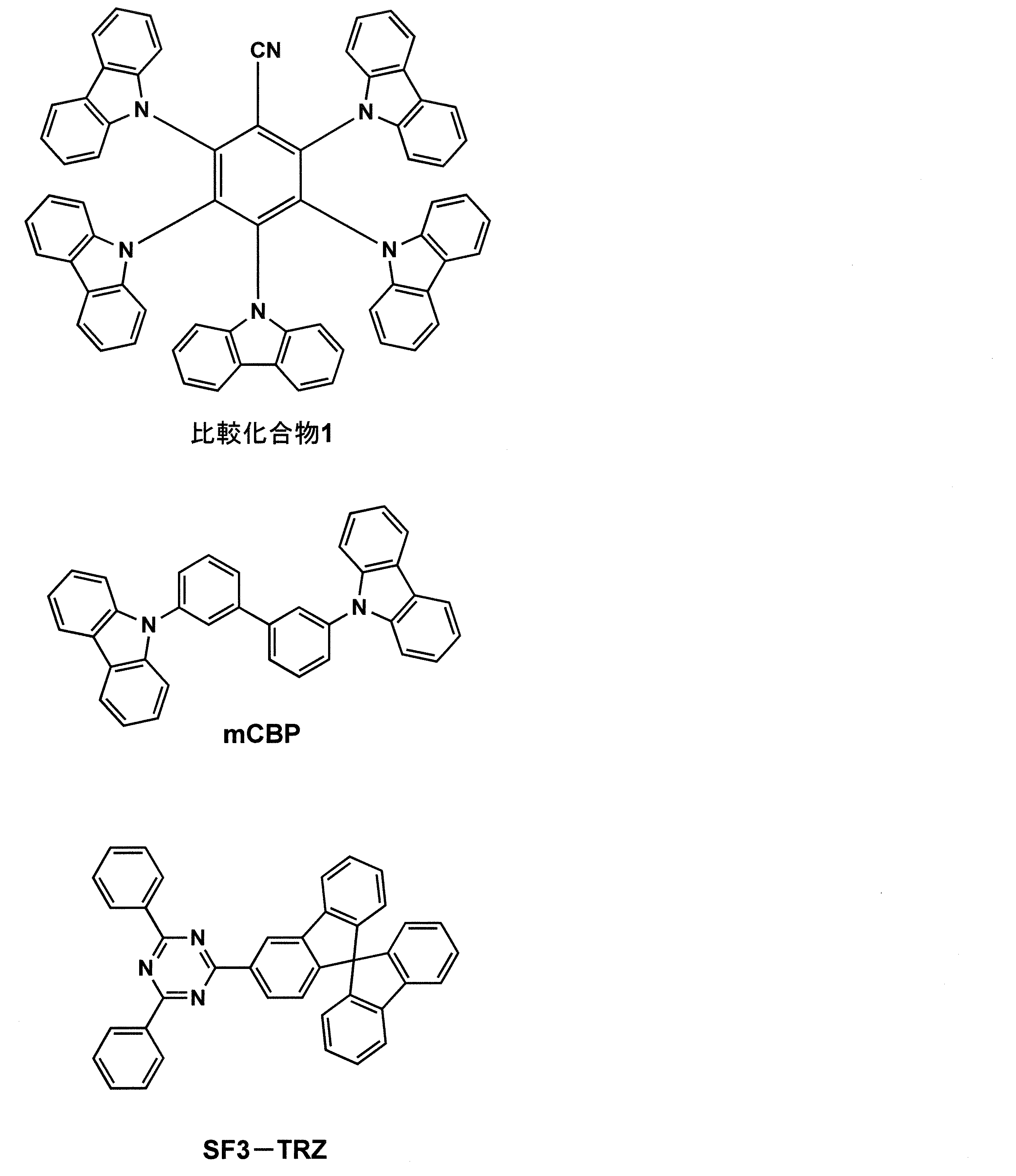
[実施例1]
<例示化合物A-3の合成>
下記スキームにより合成した。
<例示化合物A-3の合成>
下記スキームにより合成した。
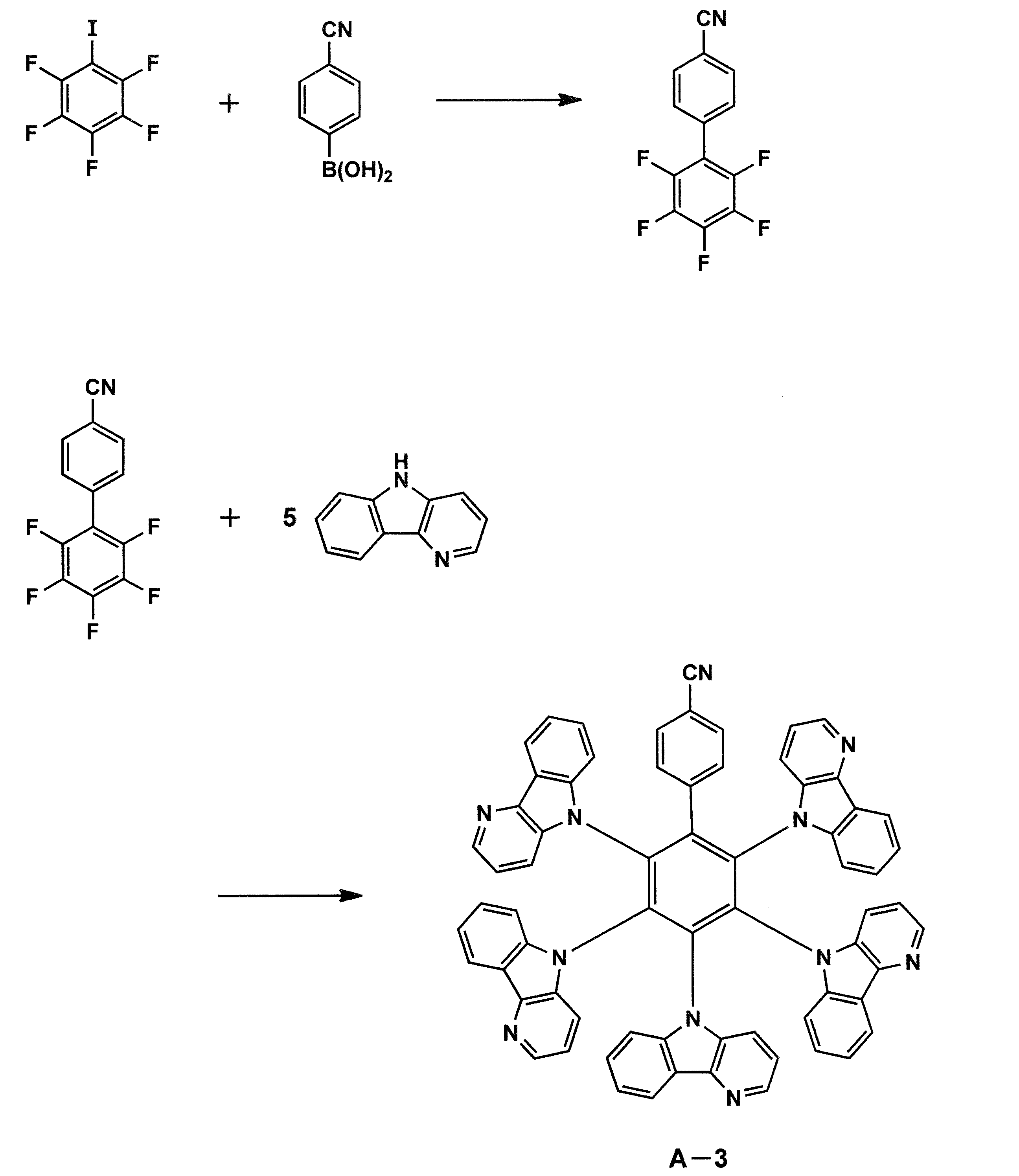
1,4-ジオキサン(50mL)中に4-シアノフェニルボロン酸(1.2g、4.1mmol)とペンタフルオロヨードベンゼン(0.6g、4.1mmol)を溶かしてトリス(ジベンジリデンアセトン)ジパラジウム(0)(Pd2(dba)3)(0.2g、0.2mmol)、K2CO3(1.7g、12.2mmol)、2-ジシクロヘキシルホスフィノ-2′,6′-ジメトキシビフェニル(S-Phos)(0.3g,0.8mmol)を加えて110℃で6時間攪拌した。反応液に水を加え、析出物をろ取した。これを再結晶して中間体1.07gを得た。
次にジメチルホルムアミド(DMF)(42mL)中に5H-ピリド[3,2-b]インドール(4.0g,23.9mmol)を溶かしNaH(1.0g、23.9mmol)を加え120℃で3時間撹拌した。その後中間体(1.07g、4.0mmol)を溶液中に加え、70℃で5時間加熱撹拌した。反応液に水を加え、析出物をろ取した。これをカラムクロマトグラフィーで精製して目的の例示化合物(A-3)3.6gを得た。
<例示化合物A-1、A-3、A-8、A-30及びA-31の合成>
主に原材料を変更した以外は前述と同様にして、例示化合物A-1、A-3、A-8、A-30及びA-31を合成した。
主に原材料を変更した以外は前述と同様にして、例示化合物A-1、A-3、A-8、A-30及びA-31を合成した。
(ΔEst及びLUMOのエネルギー準位の算出)
例示化合物A-1、A-3、A-8、A-30、A-31及び比較化合物1のΔEstを、前述した分子軌道計算用ソフトウェアの米国Gaussian社製のGaussian09を用いて算出した。
同様にして、上記化合物の置換基R1(例えば、例示化合物A-1の場合シアノカルバゾリル基)を有する一般式(2)で表される化合物のLUMOのエネルギー準位を、同様な方法で算出した。得られたLUMOのエネルギー準位を表Iに示す。

例示化合物A-1、A-3、A-8、A-30、A-31及び比較化合物1のΔEstを、前述した分子軌道計算用ソフトウェアの米国Gaussian社製のGaussian09を用いて算出した。
同様にして、上記化合物の置換基R1(例えば、例示化合物A-1の場合シアノカルバゾリル基)を有する一般式(2)で表される化合物のLUMOのエネルギー準位を、同様な方法で算出した。得られたLUMOのエネルギー準位を表Iに示す。
[実施例2]
<有機EL素子1-1の作製>
(有機EL素子1-1の作製)
陽極として100mm×100mm×1.1mmのガラス基板上にITO(インジウム・スズ酸化物)を100nm成膜した基板(NHテクノグラス社製NA45)にパターニングを行った。その後、このITO透明電極を設けた透明支持基板をイソプロピルアルコールで超音波洗浄し、乾燥窒素ガスで乾燥し、UVオゾン洗浄を5分間行った。 この透明支持基板上に、ポリ(3,4-エチレンジオキシチオフェン)-ポリスチレンスルホネート(PEDOT/PSS、Bayer社製、Baytron P Al 4083)を純水で70%に希釈した溶液を用いて3000rpm、30秒の条件下、スピンコート法により薄膜を形成した後、200℃にて1時間乾燥し、厚さ20nmの正孔注入層を設けた。
<有機EL素子1-1の作製>
(有機EL素子1-1の作製)
陽極として100mm×100mm×1.1mmのガラス基板上にITO(インジウム・スズ酸化物)を100nm成膜した基板(NHテクノグラス社製NA45)にパターニングを行った。その後、このITO透明電極を設けた透明支持基板をイソプロピルアルコールで超音波洗浄し、乾燥窒素ガスで乾燥し、UVオゾン洗浄を5分間行った。 この透明支持基板上に、ポリ(3,4-エチレンジオキシチオフェン)-ポリスチレンスルホネート(PEDOT/PSS、Bayer社製、Baytron P Al 4083)を純水で70%に希釈した溶液を用いて3000rpm、30秒の条件下、スピンコート法により薄膜を形成した後、200℃にて1時間乾燥し、厚さ20nmの正孔注入層を設けた。
その後、ポリビニルカルバゾール(重量平均分子量Mw:1100000)を1,2ジクロロベンゼンに溶かした溶液を用いて2000rpm、30秒の条件下、スピンコート法により薄膜を形成した後、120℃にて10分間乾燥し、厚さ15nmの正孔輸送層を設けた。
さらに、発光性化合物として比較化合物1とホスト化合物としてmCBPが、それぞれ10%、90%の重量%になるようトルエンに溶かした溶液を用い、2000rpm、30秒の条件下、スピンコート法により薄膜を形成した後、100℃にて10分間乾燥し、厚さ35nmの発光層を設けた。
次に、この基板を市販の真空蒸着装置の基板ホルダーに固定した。
さらに、発光性化合物として比較化合物1とホスト化合物としてmCBPが、それぞれ10%、90%の重量%になるようトルエンに溶かした溶液を用い、2000rpm、30秒の条件下、スピンコート法により薄膜を形成した後、100℃にて10分間乾燥し、厚さ35nmの発光層を設けた。
次に、この基板を市販の真空蒸着装置の基板ホルダーに固定した。
真空蒸着装置内の蒸着用るつぼの各々に、各層の構成材料を、各々素子作製に最適の量を充填した。蒸着用るつぼはモリブデン製又はタングステン製の抵抗加熱用材料で作製されたものを用いた。
真空度1×10⁻⁴Paまで減圧した後、SF3-TRZを蒸着速度1.0nm/秒で蒸着し、厚さ5nmの正孔阻止層を形成した。
その後、SF3-TRZとLiQ(8-ヒドロキシキノリノラト-リチウム)が、それぞれ50%、50%のモル%になるように蒸着速度1.0nm/秒で共蒸着し、層厚30nmの電子輸送層を形成した。
その後、SF3-TRZとLiQ(8-ヒドロキシキノリノラト-リチウム)が、それぞれ50%、50%のモル%になるように蒸着速度1.0nm/秒で共蒸着し、層厚30nmの電子輸送層を形成した。
さらに、フッ化リチウムを厚さ0.5nmで形成した後に、アルミニウム100nmを蒸着して陰極を形成した。
上記素子の非発光面側を、純度99.999%以上の高純度窒素ガスの雰囲気下で、缶状ガラスケースで覆い、電極取り出し配線を設置して、有機EL素子1-1を作製した。
上記素子の非発光面側を、純度99.999%以上の高純度窒素ガスの雰囲気下で、缶状ガラスケースで覆い、電極取り出し配線を設置して、有機EL素子1-1を作製した。
(有機EL素子1-2~1-6の作製)
発光性化合物を表IIに示すように変えた以外は有機EL素子1-1と同様の方法で有機EL素子1-2~1-6を作製した。
発光性化合物を表IIに示すように変えた以外は有機EL素子1-1と同様の方法で有機EL素子1-2~1-6を作製した。
(相対発光効率の測定)
上記作製した各有機EL素子を、室温(約25℃)で、2.5mA/cm2の定電流条件下で発光させ、発光開始直後の発光輝度を、分光放射輝度計CS-2000(コニカミノルタ社製)を用いて測定した。得られた発光輝度を、有機EL素子1-1の発光輝度に対する相対値として計算し、これを発光効率として表IIに示した。
上記作製した各有機EL素子を、室温(約25℃)で、2.5mA/cm2の定電流条件下で発光させ、発光開始直後の発光輝度を、分光放射輝度計CS-2000(コニカミノルタ社製)を用いて測定した。得られた発光輝度を、有機EL素子1-1の発光輝度に対する相対値として計算し、これを発光効率として表IIに示した。
(発光輝度半減時間の測定)
上記準備した各素子を、初期発光輝度300cd/m2で点灯したときの発光輝度半減時間(発光輝度が300cd/m2から150cd/m2まで低下するのに要する時間)をそれぞれ測定した。
そして、表IIに各素子の発光輝度半減時間を、有機EL素子1-1の発光輝度半減時間に対する相対値で示した。
上記準備した各素子を、初期発光輝度300cd/m2で点灯したときの発光輝度半減時間(発光輝度が300cd/m2から150cd/m2まで低下するのに要する時間)をそれぞれ測定した。
そして、表IIに各素子の発光輝度半減時間を、有機EL素子1-1の発光輝度半減時間に対する相対値で示した。

表IIにおいて、いずれの場合も、比較化合物1より本発明の電荷輸送性化合物の方が高い発光効率を示した。また、いずれの場合も、比較化合物1より本発明の電荷輸送性化合物の方が高い発光輝度半減時間を示した。
[実施例3]
<有機EL素子2-1の作製>
陽極として100mm×100mm×1.1mmのガラス基板上にITOを100nm成膜した基板(AvanStrate社製NA45)にパターニングを行った。その後、このITO透明電極を設けた透明支持基板をイソプロピルアルコールで超音波洗浄し、乾燥窒素ガスで乾燥し、UVオゾン洗浄を5分間行った。
この透明支持基板上に、ポリ(3,4-エチレンジオキシチオフェン)-ポリスチレンスルホネート(PEDOT/PSS、Bayer社製、Baytron P Al 4083)を純水で70%に希釈した溶液を用いて3000rpm、30秒の条件下、スピンコート法により薄膜を形成した後、200℃にて1時間乾燥し、層厚20nmの正孔注入層を設けた。
<有機EL素子2-1の作製>
陽極として100mm×100mm×1.1mmのガラス基板上にITOを100nm成膜した基板(AvanStrate社製NA45)にパターニングを行った。その後、このITO透明電極を設けた透明支持基板をイソプロピルアルコールで超音波洗浄し、乾燥窒素ガスで乾燥し、UVオゾン洗浄を5分間行った。
この透明支持基板上に、ポリ(3,4-エチレンジオキシチオフェン)-ポリスチレンスルホネート(PEDOT/PSS、Bayer社製、Baytron P Al 4083)を純水で70%に希釈した溶液を用いて3000rpm、30秒の条件下、スピンコート法により薄膜を形成した後、200℃にて1時間乾燥し、層厚20nmの正孔注入層を設けた。
その後、ポリビニルカルバゾール(重量平均分子量Mw:1100000)を1,2ジクロロベンゼンに溶かした溶液を用いて2000rpm、30秒の条件下、スピンコート法により薄膜を形成した後、120℃にて10分間乾燥し、層厚15nmの正孔輸送層を設けた。
次いで、発光性化合物として比較化合物1とホスト化合物としてmCBPが、それぞれ10%、90%の質量%になるようプロピレングリコールモノメチルエーテルアセテートに溶かしたインク組成物を用い、前述の図1に記載の構造からなるピエゾ方式インクジェットプリンターヘッドであるコニカミノルタ社製のピエゾ方式インクジェットプリンターヘッド「KM1024i」を用いて、図1に示したインクジェット印刷法による有機EL素子の製造フローに従って、40℃で、乾燥後の層厚が35nmとなる条件で正孔輸送層上に射出したのち、120℃で30分間乾燥して、発光層を形成した。
次いで、発光性化合物として比較化合物1とホスト化合物としてmCBPが、それぞれ10%、90%の質量%になるようプロピレングリコールモノメチルエーテルアセテートに溶かしたインク組成物を用い、前述の図1に記載の構造からなるピエゾ方式インクジェットプリンターヘッドであるコニカミノルタ社製のピエゾ方式インクジェットプリンターヘッド「KM1024i」を用いて、図1に示したインクジェット印刷法による有機EL素子の製造フローに従って、40℃で、乾燥後の層厚が35nmとなる条件で正孔輸送層上に射出したのち、120℃で30分間乾燥して、発光層を形成した。
次に、この基板を市販の真空蒸着装置の基板ホルダーに固定した。
真空蒸着装置内の蒸着用るつぼの各々に、各層の構成材料を、各々素子作製に最適の量を充填した。蒸着用るつぼはモリブデン製又はタングステン製の抵抗加熱用材料で作製されたものを用いた。
真空度1×10⁻⁴Paまで減圧した後、SF3-TRZを蒸着速度1.0nm/秒で蒸着し、層厚5nmの正孔阻止層を形成した。
真空蒸着装置内の蒸着用るつぼの各々に、各層の構成材料を、各々素子作製に最適の量を充填した。蒸着用るつぼはモリブデン製又はタングステン製の抵抗加熱用材料で作製されたものを用いた。
真空度1×10⁻⁴Paまで減圧した後、SF3-TRZを蒸着速度1.0nm/秒で蒸着し、層厚5nmの正孔阻止層を形成した。
その後、SF3-TRZとLiQ(8-ヒドロキシキノリノラト-リチウム)が、それぞれ50%、50%のモル%になるように蒸着速度1.0nm/秒で共蒸着し、層厚30nmの電子輸送層を形成した。
さらに、フッ化リチウムを厚さ0.5nmで形成した後に、アルミニウム100nmを蒸着して陰極を形成した。
上記素子の非発光面側を、純度99.999%以上の高純度窒素ガスの雰囲気下で、缶状ガラスケースで覆い、電極取り出し配線を設置して、有機EL素子2-1を作製した。
さらに、フッ化リチウムを厚さ0.5nmで形成した後に、アルミニウム100nmを蒸着して陰極を形成した。
上記素子の非発光面側を、純度99.999%以上の高純度窒素ガスの雰囲気下で、缶状ガラスケースで覆い、電極取り出し配線を設置して、有機EL素子2-1を作製した。
<有機EL素子2-2~2-6の作製>
発光性化合物を下記表IIIに示すように変えた以外は有機EL素子2-1と同様の方法
で有機EL素子2-2~2-6を作製した。
発光性化合物を下記表IIIに示すように変えた以外は有機EL素子2-1と同様の方法
で有機EL素子2-2~2-6を作製した。
実施例2と同様な方法で、発光効率及び発光輝度半減時間を算出し、有機EL素子2-1の値をそれぞれ100とする相対値で示した。以上の結果を表IIIに示す。

表IIIにおいて、いずれの場合も、比較化合物1より本発明の電荷輸送性化合物の方が
高い発光効率を示した。また、いずれの場合も、比較化合物1より本発明の電荷輸送性化合物の方が高い輝度半減時間を示した。
高い発光効率を示した。また、いずれの場合も、比較化合物1より本発明の電荷輸送性化合物の方が高い輝度半減時間を示した。
本発明の電荷輸送性化合物は、電荷移動/発光性薄膜の通電経時での物性変動を抑制し、発光効率及び発光素子寿命に優れており、インク組成物、有機エレクトロルミネッセンス素子材料、発光材料、発光性薄膜及び有機エレクトロルミネッセンス素子に好ましく適用することができる。
1、101 有機EL素子
2 基材
30、100 インクジェットヘッド
31、39 ポンプ
32 フィルター
33 配管分岐
34 廃液タンク
35 制御部
36、37、38A、38B タンク
56 筐体
57 キャップ受板
59 カバー部材
61 ノズルプレート
62 キャップ受板取り付け部
68 取り付け用孔
71 ノズル用開口部
81a 第1ジョイト
81b 第2ジョイント
82 第3ジョイント
102 ガラスカバー
105 陰極
106 有機EL層
107 透明電極付きガラス基板
108 窒素ガス
109 捕水剤
2 基材
30、100 インクジェットヘッド
31、39 ポンプ
32 フィルター
33 配管分岐
34 廃液タンク
35 制御部
36、37、38A、38B タンク
56 筐体
57 キャップ受板
59 カバー部材
61 ノズルプレート
62 キャップ受板取り付け部
68 取り付け用孔
71 ノズル用開口部
81a 第1ジョイト
81b 第2ジョイント
82 第3ジョイント
102 ガラスカバー
105 陰極
106 有機EL層
107 透明電極付きガラス基板
108 窒素ガス
109 捕水剤
Claims (12)
- 下記一般式(1)で表される構造を有し、最低励起一重項エネルギー準位と最低励起三重項エネルギー準位とのエネルギー差の絶対値ΔEstが、0.30eV以下であることを特徴とする電荷輸送性化合物。

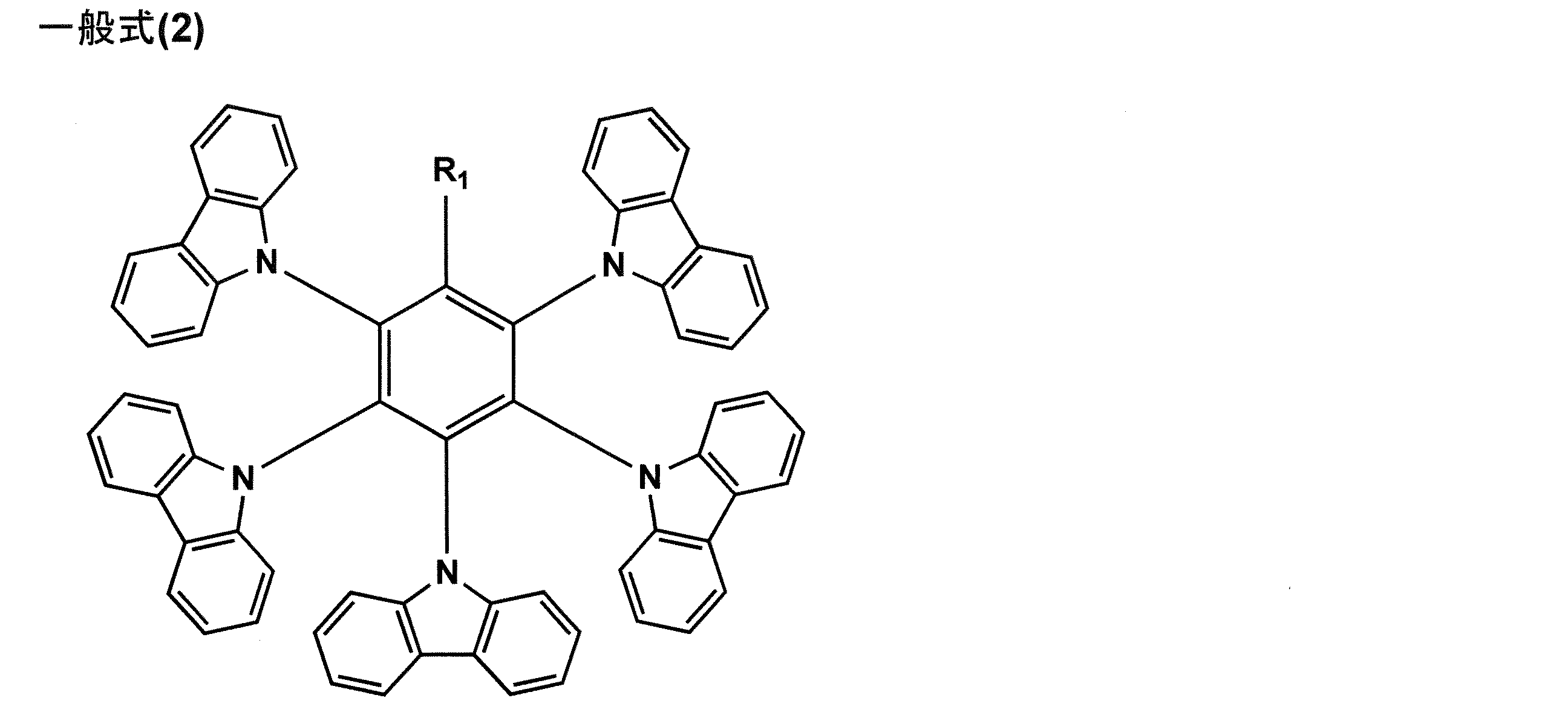
- 前記一般式(1)において、前記D1~D5のうち、少なくとも二つが、キラリティ発生部位を有することを特徴とする請求項1に記載の電荷輸送性化合物。
- 前記一般式(1)において、前記D1~D5が、置換基を有していても良いカルバゾリル基又はカルボリニル基を表すことを特徴とする請求項1又は請求項2に記載の電荷輸送性化合物。
- 前記一般式(1)において、前記R1が、置換基を有していてもよい芳香族基であることを特徴とする請求項1から請求項3までのいずれか一項に記載の電荷輸送性化合物。
- 前記一般式(1)において、前記R1が、キラリティ発生部位を有することを特徴とする請求項1から請求項4までのいずれか一項に記載の電荷輸送性化合物。
- 請求項1から請求項5までのいずれか一項に記載の電荷輸送性化合物を製造する電荷輸送性化合物の製造方法であって、
求核置換反応により前記D1~D5をそれぞれ導入することを特徴とする電荷輸送性化合物の製造方法。 - 請求項1から請求項5までのいずれか一項に記載の電荷輸送性化合物を含有することを特徴とするインク組成物。
- 請求項1から請求項5までのいずれか一項に記載の電荷輸送性化合物を含有することを特徴とする有機エレクトロルミネッセンス素子材料。
- 請求項1から請求項5までのいずれか一項に記載の電荷輸送性化合物を含有し、前記電荷輸送性化合物が蛍光を放射することを特徴とする発光材料。
- 前記蛍光が、遅延蛍光であることを特徴とする請求項9に記載の発光材料。
- 請求項1から請求項5までのいずれか一項に記載の電荷輸送性化合物を含有することを特徴とする発光性薄膜。
- 陽極と、陰極と、前記陽極と前記陰極との間に設けられた発光層とを含み、前記発光層の少なくとも一層が、請求項1から請求項5までのいずれか一項に記載の電荷輸送性化合物を含有することを特徴とする有機エレクトロルミネッセンス素子。
Priority Applications (1)
| Application Number | Priority Date | Filing Date | Title |
|---|---|---|---|
| JP2021507173A JPWO2020189283A1 (ja) | 2019-03-18 | 2020-03-04 |
Applications Claiming Priority (2)
| Application Number | Priority Date | Filing Date | Title |
|---|---|---|---|
| JP2019050018 | 2019-03-18 | ||
| JP2019-050018 | 2019-03-18 |
Publications (1)
| Publication Number | Publication Date |
|---|---|
| WO2020189283A1 true WO2020189283A1 (ja) | 2020-09-24 |
Family
ID=72520749
Family Applications (1)
| Application Number | Title | Priority Date | Filing Date |
|---|---|---|---|
| PCT/JP2020/009168 Ceased WO2020189283A1 (ja) | 2019-03-18 | 2020-03-04 | 電荷輸送性化合物及びその製造方法、インク組成物、有機エレクトロルミネッセンス素子材料等 |
Country Status (2)
| Country | Link |
|---|---|
| JP (1) | JPWO2020189283A1 (ja) |
| WO (1) | WO2020189283A1 (ja) |
Cited By (3)
| Publication number | Priority date | Publication date | Assignee | Title |
|---|---|---|---|---|
| JPWO2020189236A1 (ja) * | 2019-03-18 | 2020-09-24 | ||
| US20220190257A1 (en) * | 2019-03-19 | 2022-06-16 | Konica Minolta, Inc. | Functional film, method for forming same, and organic electroluminescent element |
| WO2023140374A1 (ja) * | 2022-01-24 | 2023-07-27 | 株式会社Kyulux | 化合物、発光材料および発光素子 |
Citations (8)
| Publication number | Priority date | Publication date | Assignee | Title |
|---|---|---|---|---|
| WO2015022835A1 (ja) * | 2013-08-14 | 2015-02-19 | コニカミノルタ株式会社 | 有機エレクトロルミネッセンス素子、照明装置、表示装置及び蛍光発光性化合物 |
| WO2016181846A1 (ja) * | 2015-05-08 | 2016-11-17 | コニカミノルタ株式会社 | π共役系化合物、有機エレクトロルミネッセンス素子材料、発光材料、発光性薄膜、有機エレクトロルミネッセンス素子、表示装置及び照明装置 |
| CN106966955A (zh) * | 2017-04-21 | 2017-07-21 | 瑞声光电科技(常州)有限公司 | 联苯化合物及发光器件 |
| WO2017216299A1 (de) * | 2016-06-15 | 2017-12-21 | Technische Universität Dresden | Emittermoleküle auf basis dual fluoreszierender benzol-(poly)carboxylat-akzeptoren |
| WO2019009307A1 (ja) * | 2017-07-03 | 2019-01-10 | 三菱ケミカル株式会社 | Oled素子形成用組成物及びoled素子 |
| KR20190018397A (ko) * | 2017-08-14 | 2019-02-22 | 주식회사 엘지화학 | 함질소 고리 화합물 및 이를 포함하는 유기 발광 소자 |
| CN109651406A (zh) * | 2019-01-23 | 2019-04-19 | 苏州久显新材料有限公司 | 热激活延迟荧光化合物、发光材料及有机电致发光器件 |
| JP2019142780A (ja) * | 2018-02-15 | 2019-08-29 | 国立大学法人愛媛大学 | 新規な芳香族化合物 |
Family Cites Families (4)
| Publication number | Priority date | Publication date | Assignee | Title |
|---|---|---|---|---|
| CN111051471A (zh) * | 2017-09-01 | 2020-04-21 | 九州有机光材股份有限公司 | 用于有机发光二极管中的组合物 |
| WO2020059520A1 (ja) * | 2018-09-21 | 2020-03-26 | コニカミノルタ株式会社 | ベンゾニトリル誘導体及びその製造方法、インク組成物、有機エレクトロルミネッセンス素子材料、発光材料、電荷輸送材料、発光性薄膜及び有機エレクトロルミネッセンス素子 |
| WO2020189236A1 (ja) * | 2019-03-18 | 2020-09-24 | コニカミノルタ株式会社 | 有機膜及び有機エレクトロルミネッセンス素子 |
| WO2020189330A1 (ja) * | 2019-03-19 | 2020-09-24 | コニカミノルタ株式会社 | 機能性膜、その形成方法及び有機エレクトロルミネッセンス素子 |
-
2020
- 2020-03-04 JP JP2021507173A patent/JPWO2020189283A1/ja active Pending
- 2020-03-04 WO PCT/JP2020/009168 patent/WO2020189283A1/ja not_active Ceased
Patent Citations (8)
| Publication number | Priority date | Publication date | Assignee | Title |
|---|---|---|---|---|
| WO2015022835A1 (ja) * | 2013-08-14 | 2015-02-19 | コニカミノルタ株式会社 | 有機エレクトロルミネッセンス素子、照明装置、表示装置及び蛍光発光性化合物 |
| WO2016181846A1 (ja) * | 2015-05-08 | 2016-11-17 | コニカミノルタ株式会社 | π共役系化合物、有機エレクトロルミネッセンス素子材料、発光材料、発光性薄膜、有機エレクトロルミネッセンス素子、表示装置及び照明装置 |
| WO2017216299A1 (de) * | 2016-06-15 | 2017-12-21 | Technische Universität Dresden | Emittermoleküle auf basis dual fluoreszierender benzol-(poly)carboxylat-akzeptoren |
| CN106966955A (zh) * | 2017-04-21 | 2017-07-21 | 瑞声光电科技(常州)有限公司 | 联苯化合物及发光器件 |
| WO2019009307A1 (ja) * | 2017-07-03 | 2019-01-10 | 三菱ケミカル株式会社 | Oled素子形成用組成物及びoled素子 |
| KR20190018397A (ko) * | 2017-08-14 | 2019-02-22 | 주식회사 엘지화학 | 함질소 고리 화합물 및 이를 포함하는 유기 발광 소자 |
| JP2019142780A (ja) * | 2018-02-15 | 2019-08-29 | 国立大学法人愛媛大学 | 新規な芳香族化合物 |
| CN109651406A (zh) * | 2019-01-23 | 2019-04-19 | 苏州久显新材料有限公司 | 热激活延迟荧光化合物、发光材料及有机电致发光器件 |
Non-Patent Citations (5)
Cited By (3)
| Publication number | Priority date | Publication date | Assignee | Title |
|---|---|---|---|---|
| JPWO2020189236A1 (ja) * | 2019-03-18 | 2020-09-24 | ||
| US20220190257A1 (en) * | 2019-03-19 | 2022-06-16 | Konica Minolta, Inc. | Functional film, method for forming same, and organic electroluminescent element |
| WO2023140374A1 (ja) * | 2022-01-24 | 2023-07-27 | 株式会社Kyulux | 化合物、発光材料および発光素子 |
Also Published As
| Publication number | Publication date |
|---|---|
| JPWO2020189283A1 (ja) | 2020-09-24 |
Similar Documents
| Publication | Publication Date | Title |
|---|---|---|
| JP6754185B2 (ja) | 有機エレクトロルミネッセンス素子、表示装置、照明装置及び電子デバイス用有機機能性材料 | |
| JP6761463B2 (ja) | 発光性薄膜及び有機エレクトロルミネッセンス素子 | |
| KR102146446B1 (ko) | π 공액계 화합물, 유기 일렉트로루미네센스 소자 재료, 발광 재료, 발광성 박막, 유기 일렉트로루미네센스 소자, 표시 장치 및 조명 장치 | |
| KR102808074B1 (ko) | 방향족 복소환 유도체, 그것을 사용한 유기 일렉트로루미네센스 소자, 조명 장치 및 표시 장치 | |
| KR102151027B1 (ko) | 유기 일렉트로루미네센스 소자, 유기 일렉트로루미네센스 소자의 제조 방법, 표시 장치 및 조명 장치 | |
| JP6761662B2 (ja) | 有機エレクトロルミネッセンス素子、表示装置及び照明装置 | |
| JP6802189B2 (ja) | 薄膜、及び有機エレクトロルミネッセンス素子 | |
| JP6705148B2 (ja) | π共役系化合物、有機エレクトロルミネッセンス素子材料、発光材料、発光性薄膜、有機エレクトロルミネッセンス素子、表示装置及び照明装置 | |
| WO2018186462A1 (ja) | 蛍光発光性化合物、有機材料組成物、発光性膜、有機エレクトロルミネッセンス素子材料及び有機エレクトロルミネッセンス素子 | |
| JPWO2016017514A1 (ja) | 有機エレクトロルミネッセンス素子、発光性薄膜、表示装置及び照明装置 | |
| JP5998745B2 (ja) | 有機エレクトロルミネッセンス素子、表示装置、照明装置及び有機エレクトロルミネッセンス素子の製造方法 | |
| JP6686748B2 (ja) | 有機エレクトロルミネッセンス素子、表示装置、照明装置、π共役系化合物 | |
| WO2018008721A1 (ja) | 有機エレクトロルミネッセンス素子、表示装置、照明装置 | |
| JP2017108006A (ja) | 有機エレクトロルミネッセンス素子、表示装置及び照明装置 | |
| WO2020189117A1 (ja) | π共役系化合物、π共役系化合物の製造方法、インク組成物、有機エレクトロルミネッセンス素子材料、発光材料、電荷輸送材料、発光性薄膜及び有機エレクトロルミネッセンス素子 | |
| JP7081898B2 (ja) | 有機エレクトロルミネッセンス素子、表示装置及び照明装置 | |
| JP6942127B2 (ja) | 有機エレクトロルミネッセンス素子、表示装置、照明装置 | |
| US20210343947A1 (en) | Benzonitrile derivative and manufacturing method therefor, ink composition, organic electroluminescent element material, light-emitting material, charge transport material, light-emitting thin film, and organic electroluminescent element | |
| JPWO2020059520A1 (ja) | ベンゾニトリル誘導体及びその製造方法、インク組成物、有機エレクトロルミネッセンス素子材料、発光材料、電荷輸送材料、発光性薄膜及び有機エレクトロルミネッセンス素子 | |
| WO2018173600A1 (ja) | 有機エレクトロルミネッセンス素子 | |
| WO2020189283A1 (ja) | 電荷輸送性化合物及びその製造方法、インク組成物、有機エレクトロルミネッセンス素子材料等 | |
| WO2020189236A1 (ja) | 有機膜及び有機エレクトロルミネッセンス素子 | |
| WO2016194865A1 (ja) | 有機エレクトロルミネッセンス素子 | |
| JP2022075698A (ja) | π共役系化合物、有機エレクトロルミネッセンス素子材料、発光材料、電荷輸送材料、発光性薄膜、有機エレクトロルミネッセンス素子、表示装置及び照明装置 |
Legal Events
| Date | Code | Title | Description |
|---|---|---|---|
| 121 | Ep: the epo has been informed by wipo that ep was designated in this application |
Ref document number: 20772839 Country of ref document: EP Kind code of ref document: A1 |
|
| ENP | Entry into the national phase |
Ref document number: 2021507173 Country of ref document: JP Kind code of ref document: A |
|
| NENP | Non-entry into the national phase |
Ref country code: DE |
|
| 122 | Ep: pct application non-entry in european phase |
Ref document number: 20772839 Country of ref document: EP Kind code of ref document: A1 |