WO2020189064A1 - ソフトウェア無線機 - Google Patents
ソフトウェア無線機 Download PDFInfo
- Publication number
- WO2020189064A1 WO2020189064A1 PCT/JP2020/004293 JP2020004293W WO2020189064A1 WO 2020189064 A1 WO2020189064 A1 WO 2020189064A1 JP 2020004293 W JP2020004293 W JP 2020004293W WO 2020189064 A1 WO2020189064 A1 WO 2020189064A1
- Authority
- WO
- WIPO (PCT)
- Prior art keywords
- control
- control information
- module
- interface
- communication method
- Prior art date
- Legal status (The legal status is an assumption and is not a legal conclusion. Google has not performed a legal analysis and makes no representation as to the accuracy of the status listed.)
- Ceased
Links
Images





Classifications
-
- G—PHYSICS
- G06—COMPUTING OR CALCULATING; COUNTING
- G06F—ELECTRIC DIGITAL DATA PROCESSING
- G06F15/00—Digital computers in general; Data processing equipment in general
- G06F15/76—Architectures of general purpose stored program computers
- G06F15/78—Architectures of general purpose stored program computers comprising a single central processing unit
-
- H—ELECTRICITY
- H04—ELECTRIC COMMUNICATION TECHNIQUE
- H04B—TRANSMISSION
- H04B1/00—Details of transmission systems, not covered by a single one of groups H04B3/00 - H04B13/00; Details of transmission systems not characterised by the medium used for transmission
-
- H—ELECTRICITY
- H04—ELECTRIC COMMUNICATION TECHNIQUE
- H04B—TRANSMISSION
- H04B1/00—Details of transmission systems, not covered by a single one of groups H04B3/00 - H04B13/00; Details of transmission systems not characterised by the medium used for transmission
- H04B1/38—Transceivers, i.e. devices in which transmitter and receiver form a structural unit and in which at least one part is used for functions of transmitting and receiving
Definitions
- This disclosure relates to software defined radio.
- a software defined radio is a radio that can support multiple wireless communication methods with the same hardware resources in the radio by switching the execution program of the radio by a software program.
- the module configuration in the software defined radio is configured by downloading a file that defines the desired function from the network and reconfiguring the module with the desired communication method using the partial reconfigure technology. Will be changed to realize multiple wireless communication methods.
- the reconfigurable module equipped with the wireless communication method is controlled by sending control information by the CPU, and the interface of the reconfigurable module equipped with the communication method is connected to the CPU by a bus that transfers control information.
- the interface of the reconfigurable module equipped with the communication method is connected to the CPU only by the data bus, the bus that passes the control information when adding the reconfigurable module that requires the control information specific to the communication method Since it does not exist, it is not possible to add a communication method.
- the developed reconfigurable module is diverted to the software defined radio of the next development, if the bus does not exist in the software defined radio of the next development, the developed reconfigurable module cannot be used.
- the resources used will increase, wiring will become difficult, reconfigurable modules that require large-scale resources cannot be used, and the communication methods that can be used may be limited. There is.
- An object of the present disclosure is to provide a software defined radio having a common interface for hardware resources between a CPU and a reconfigurable module.
- the software defined radio has a plurality of hardware modules, and the wireless communication software that controls the plurality of hardware modules is downloaded from the outside to realize the radio function.
- the hardware module is composed of at least one of a CPU, a reconfigurable module, and a static module.
- the reconfigurable module and the interface with the static module are classified into a predetermined pattern.
- Control information is acquired from the upper level of the software defined radio.
- a control ID is assigned to the control information, and the CPU divides the control ID pattern into control information common to the communication method and control information unique to the communication method, and serves as an interface between the reconfigurable module and the static module.
- FIG. 1 is a diagram illustrating a software defined radio.
- FIG. 2 is a diagram showing a software structure of a software defined radio.
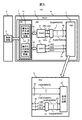
- FIG. 3 is a diagram illustrating a semiconductor device constituting a software defined radio.
- FIG. 4 is a diagram illustrating a control ID pattern.
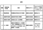
- FIG. 5 is a diagram illustrating an example of control information.
- FIG. 6 is a diagram showing a data structure of control information common to communication methods stored in a memory device.
- FIG. 7 is a diagram showing a data structure of control information unique to the communication method stored in the memory device.
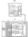
- FIG. 8 is a diagram illustrating a configuration of a reconfigurable module when a communication method is newly developed.
- FIG. 9 is a diagram illustrating a configuration when the developed reconfigurable module 2 is used in a newly developed software defined radio.
- the software defined radio (100) is composed of a CPU (1), a reconfigurable module (2), and a static module (3).
- a control ID is assigned to the control information acquired from the upper level, and the CPU (1) divides the control ID pattern into control information (5a) commonly used in the communication method and control information (5b) specific to the communication method.
- the interfaces of the CPU (1) and the reconfigurable module (2) and the static module (3) are classified into predetermined interfaces. There are two types of predetermined interfaces, an interface (36, 21) for passing control information (5a) commonly used in communication methods and an interface (37,) for passing control information (5b) specific to communication methods. 22). Both interfaces use memory devices (31, 32).
- the control information (5a) used in common with the communication method has a table in the memory device (31), and the interfaces (36, 21) of the static module (3) and the reconfigurable module (2) have a predetermined bus format (plurality). Connect with the control ID bus line).
- the total number of IDs, the ID number, the data length (LENGTH), and the data (DATA) are written in the memory device (32), and the control information (5b) is stored in the reconfigurable module (2). Convert to the required bus format (multiple control ID bus lines).
- the interface (37, 22) between the static module (3) and the reconfigurable module (2) has a predetermined bus format (address, data, enable).
- the interfaces (36, 21) for passing the control information (5a) commonly used in the communication methods are the same in all communication methods, there is no increase or decrease, and even if the communication method is changed, the interface (36, 21) 21) does not need to be changed.
- the interface can be standardized, so that the design of each hardware module is simplified. It is possible to improve the design efficiency.
- FIG. 1 shows an outline of the software defined radio 100.
- the hardware module of the software defined radio 100 includes an antenna 101, a high frequency unit 102, an A / D / D / A unit 103, a digital signal processing unit 104, and a control unit 105.
- the antenna 101 transmits and receives radio frequency signals.
- the high frequency unit 102 converts the received signal in the radio frequency band received by the antenna 101 into a received signal in the low frequency band, or converts the transmitted signal in the low frequency band into a transmitted signal in the radio frequency band.
- the A / D / D / A unit 103 converts the received analog signal into a digital signal, or converts the transmitted digital signal into an analog signal.
- the digital signal processing unit 104 performs processing such as coding of the transmission signal and decoding of the received signal.
- the control unit 105 includes, for example, a memory for storing a software program and a CPU for executing the software program stored in the memory, and receives control from the control terminal 107 via the network 106 and hardware of the software defined radio. Control the module.
- FIG. 2 shows the software structure of the software defined radio 100.
- the hardware modules 220 to 222 correspond to the high frequency unit 102, the A / D / D / A unit 103, and the digital signal processing unit 104 in FIG. 1, respectively.
- the hardware device drivers 210 to 212 drive these hardware modules 220 to 222, respectively. These operate on a predetermined OS (Operating System) 209, but the application and the OS / hardware can be separated by the CORBA (Common Object Request Broker Architecture) middleware 208.
- OS Operating System
- CORBA Common Object Request Broker Architecture
- the environmental software 215 is a software program that must be always started in order for the software radio 100 to operate, and is a user interface software 201, a domain management software 202, a hardware management software 204, and a hardware control software 205 to 207. It is included.
- the hardware control software 205 to 207 are also provided corresponding to the hardware device drivers 210 to 212, respectively, and are higher-level software programs that control them.
- wireless functions such as filters, modulation / demodulation, equalization, and synchronization functions are programmable, and by rewriting the software program, the radio parameters such as modulation method, transmission / reception frequency, bandwidth, and transmission speed are unique to the system. It is possible to change the wireless function of.
- These rewritable software programs are wireless communication software 203. Therefore, the wireless communication software 203 can be started even when the power is turned on, but most of them are started based on the instruction from the user interface software 201.
- the user interface software 201 connects and communicates with the domain management software 202 and the wireless communication software 203.
- the domain management software 202 connects to the hardware management software 204 in addition to the user interface software 201, and the hardware management software 204 connects to the hardware control software 205, 206, 207.
- the hardware control software 205, 206, 207 connects the wireless communication software 203 and the hardware device drivers 210, 211,212, and the wireless communication software 203 connects the user interface software 201 and the hardware control software 205, 206, 207. To do.
- FIG. 3 shows the semiconductor device 10 constituting the software defined radio 100.
- the semiconductor device 10 constituting the software defined radio 100 can dynamically change the hardware configuration and connections with the CPU 1 configured as a soft processor with a general-purpose memory of FPGA (Field Programmable Gate Array) and a logic circuit (programmatically). It is composed of a reconfigurable module (RM) 2 that can be reconfigured) and a static module (SM) 3 that can be set by a program such as hardware configuration and connection, but does not change dynamically.
- the CPU 1 and the reconfigurable module 2 are drawn as if they are surrounded by the static module 3, but the present invention is not limited to this.
- the CPU 1, the reconfigurable module 2, and the static module 3 may be arranged in separate regions on the chip of the semiconductor device 10.
- the control unit 105 of FIG. 1 includes a CPU 1, and the digital signal processing unit 104 is composed of a reconfigurable module 2.
- the hardware module is composed of a CPU 1 and at least one of a reconfigurable module 2 and / or a static module 3.
- the CPU 1 can read the control information 5 stored in the upper module 4.
- the control information 5 includes control information 5a used in common in the communication method and control information 5b used in the communication method.
- a predetermined control ID is assigned to each of the control information 5a and 5b.
- the CPU 1 determines the pattern of the control ID in the read control information 5, distributes the control information 5 into the control information 5a and the control information 5b, and divides the control information 5 into the control information 5a and the control information 5b inside the CPU 1. It is stored in the memory unit 1a provided in.
- FIG. 4 is a diagram illustrating a control ID pattern.
- FIG. 4 shows an example when the control ID is represented by a 16-bit size.
- the 16th bit of the control ID pattern of the control information 5a used in common with the communication method is "0 (zero)".
- the 16th bit of the control ID pattern of the control information 5b used unique to the communication method is "1".
- the CPU 1 distributes the control information 5a and the control information 5b based on whether the 16th bit is "0 (zero)" or the 16th bit is "1" in the control ID pattern.
- the minimum control ID of the control information 5a common to the communication method is 0x0000
- the maximum control ID is 0x7FFF.
- the minimum control ID is 0x8000 and the maximum control ID is 0xFFFF.
- FIG. 5 is a diagram illustrating an example of control information.
- the content of the control information 5a common to the communication method includes the frequency information setting, the transmission permission setting, and the transmission output setting, as shown in the control ID pattern as being common to the communication method.
- the frequency information setting relates to control for switching frequencies.
- the transmission permission setting relates to a control for permitting transmission.
- the transmit output setting relates to controlling the level of the transmit output.
- the control information 5b specific to the communication method includes the mode setting so as to indicate that it is unique to the communication method. If the reconfigurable module 2 is a circuit that performs AM (amplitude) modulation, the mode setting corresponds to the AM modulation mode setting. If the reconfigurable module 2 is a circuit that performs FM (frequency) modulation, the mode setting corresponds to the FM modulation mode setting.
- FIG. 5 also shows a connection interface between the static module 3 and the reconfigurable module 2.
- the control ID bus is used as the connection interface
- the control information 5b specific to the communication method the address bus, the data bus, and the enable signal are used as the connection interface. That is, based on the control ID pattern, the connection interface of the control information 5a common to the communication method is the control ID bus, and the connection interface of the control information 5b specific to the communication method is the address bus, the data bus, and the enable signal. ..
- the connection interface between the static module 3 and the reconfigurable module 2 will be described later.
- the static module 3 includes a memory device (RAM 1) 31, a memory device (RAM 2) 32, a read circuit 33 of the memory device (RAM 1) 31, a bus 34, a bus 35, a first interface 36, and a second interface. 37 and.
- the CPU 1 writes the control information 5a common to the communication method to each address of the memory device 31 as a data table for each control ID via the bus 34.
- the internal information of the memory device 31 is shown in FIG. 6 (FIG. 6 will be described later).
- the data table for each control ID written in the memory device 31 is read by the read circuit 33.
- the read circuit 33 accesses the memory device 31 by using the address bus AB1, the data bus DB1, and the enable signal line EN1, and reads out the data table for each control ID written in the memory device 31.
- the read circuit 33 converts the data table for each control ID read from the memory device 31 into data for each control ID.
- the first interface 36 is configured as a control ID bus including a plurality of control ID bus lines B1 to Bn.
- Each of the plurality of control ID bus lines B1 to Bn is provided for each control ID (0x0000 to 0x7XXX). That is, the plurality of control ID bus lines B1 to Bn are the control ID bus lines Bn provided for the control ID bus lines B1 to control ID 0x7XXX (denoted by 0x7XXXID) provided for the control ID 0x0000 (indicated as 0x0000 ID). Consists of.
- Each of the data for each control ID converted by the read circuit 33 is supplied to the corresponding control ID bus line B1 (0x0000ID) to the control ID bus line Bn (0x7XXXID).
- the first interface 36 will be connected to the reconfigurable module 2. Therefore, the control information 5a read out by the first interface 36 is supplied to the reconfigurable module 2.
- the CPU 1 writes the control information 5b peculiar to the communication method into the memory device 32 via the bus 35 as the total number of IDs, the ID information, the length of the data (DATA) (LENGTH), and the data (DATA).
- the internal information of the memory device 32 is shown in FIG. 7 (FIG. 7 will be described later).
- the memory device 32 is connected to the second interface 37.
- the second interface 37 includes an address bus AB2, a data bus DB2, and an enable signal line EN2.
- the control information 5b written in the memory device 32 can be read out by using the second interface 37.
- the second interface 37 will be connected to the reconfigurable module 2. Therefore, the control information 5b read by the second interface 37 is supplied to the reconfigurable module 2.
- the reconfigurable module 2 includes a third interface 21, a fourth interface 22, a read circuit 23, a communication system circuit 24, and an internal bus 25.
- the third interface 21 is provided for connecting to the first interface 36, and is an interface for acquiring control information 5a common to communication methods. Similar to the first interface 36, the third interface 21 is configured as a control ID bus including a plurality of control ID bus lines C1 to Cn. Each of the plurality of control ID bus lines C1 to Cn is provided for each control ID (0x0000 to 0x7XXX).
- the plurality of control ID bus lines C1 to Cn are the control ID bus lines provided for the control ID 0x0000 (indicated as 0x0000 ID) to the control ID bus lines C1 (0x0000 ID) to the control ID 0x7XXX (indicated as 0x7XXX ID). It is composed of (0x7XXXID).
- the control ID bus line C1 (0x0000ID) to control ID bus line C1 (0x7XXXID) of the third interface 21 and the control ID bus line B1 (0x0000ID) to control ID bus line Bn (0x7XXXID) of the first interface 36 are the same.
- the control ID bus lines provided for the control ID will be connected to each other. Therefore, the control information 5a common to the communication method is supplied to the third interface 21.
- the fourth interface 22 is provided for connecting to the second interface 37, and is used as an interface for acquiring control information 5b.
- the fourth interface 22 includes an address bus AB3, a data bus DB3, and an enable signal line EN3.
- the address bus AB3, the data bus DB3, and the enable signal line EN3 are connected to the address bus AB2, the data bus DB2, and the enable signal line EN2 of the second interface 37, respectively.
- the read circuit 23 is provided to read the control information 5b unique to the communication method stored in the memory device 32.
- the read circuit 23 accesses the memory device 32 by using the address buses AB1 and AB2, the data buses DB1 and DB2, and the enable signal lines EN1 and EN2.
- the read circuit 23 reads the start address in which the control information 5b of the memory device 32 is stored, confirms the total number of IDs, reads the data (DATA) corresponding to the total number of IDs, converts the data (DATA) into the format of the internal bus 25, and converts the data (DATA) into the format of the internal bus 25. It is supplied to the communication system circuit 24.
- the internal bus 25 is configured as a control ID bus including a plurality of control ID bus lines D1 to Dm.
- Each of the plurality of control ID bus lines D1 to Dm is provided for each control ID (0x8000 to 0x8XXX). That is, the plurality of control ID bus lines D1 to Dm are the control ID bus lines Dm provided for the control ID bus lines D1 to control ID 0x8XXX (denoted by 0x8XXXID) provided for the control ID 0x8000 (denoted as 0x8000ID). Consists of.
- the read circuit 23 converts the control information 5b from the memory device 31 into data for each control ID, and supplies the control information 5b to the corresponding control ID bus line D1 (0x8000ID) to the control ID bus line Dm (0x8XXXID).
- the communication system circuit 24 is desired to perform frequency information setting, transmission permission setting, transmission output setting, and mode setting based on the acquired control information 5a common to the communication system and control information 5b specific to the communication system. It is set to correspond to the communication method of.
- the third interface 21 (plurality of control ID bus lines C1 to Cn) used for acquiring the control information 5a common to the communication methods is the same in all the communication methods, so that there is no increase or decrease in communication. Even if the method is changed, it is not necessary to change the third interface 21.
- the control information 5b specific to the communication method differs depending on the communication method, but even if the communication method is changed, the internal information of the control information 5b stored in the memory device 32 and the internal bus 25 of the reconfigurable module 2 ( Only the number of control ID bus lines of the plurality of control ID bus lines D1 to Dm) is changed, and it is not necessary to change the fourth interface 22 which is an interface with the static module 3.
- FIG. 6 is a diagram showing a data structure of control information common to communication methods stored in a memory device.
- the address is shown in the vertical direction and the number of bits (BIT) is shown in the horizontal direction.
- the number of bits (BIT) is 8 bits from 0 to 7.
- the data structure 11 includes an address 12 assigned to each control ID and an area 13 for writing data (DATA) indicating control information of each control ID.
- DATA data indicating control information of each control ID.
- the data (DATA) of the control ID 0x0000 is 32 bits and is written to the addresses 0x0000 to 0x0003.
- the data (DATA) of the control ID 0x0001 is 16 bits and is written to the addresses 0x0004 to 0x0005.
- Each data (DATA) of control ID 0x0002 to control ID 0xXXXXX is also written to the corresponding address.
- the update data is written to the addresses 0x0000 to 0x0003, and when the data (DATA) of the control ID 0x0001 is updated, the update data is written to the addresses 0x0004 to 0x0005.
- FIG. 7 is a diagram showing a data structure of control information unique to the communication method stored in the memory device.
- the address is shown in the vertical direction and the number of bits (BIT) is shown in the horizontal direction.
- the number of bits (BIT) is 8 bits from 0 to 7.
- the data structure 14 has an area 16 for writing the total number of IDs at the beginning of the address 15, an area 17 for writing the control ID number (ID No.), and an area for writing the data (DATA) data length (LENGTH). 18. It is composed of an area 19 for writing data (DATA) indicating control information of a control ID.
- the area 16 is assigned to addresses 0x0000 to 0x0003.
- the area 17 is assigned to the addresses 0x0004 to 0x0005 when the control ID number is 16 bits.
- the region 18 is assigned to the addresses 0x0006 to 0x0007 when the data length (LENGTH) is represented by 16 bits.
- the area 19 is assigned to the addresses 0x0008 to 0x000D when the data (DATA) is 48 bits.
- ID number (ID) corresponding to the value of the total number of IDs written in the area 16.
- the set of No), data length (LENGTH), and data (DATA) is written for the value of the total number of IDs written in the area 16. For example, if three control information is transmitted from the CPU 1, 3 is written as the total number of IDs in the area 16 for writing the total number of IDs, and then the ID number (ID No.), the data length (LENGTH), and the data (DATA). ) Is written in three sets.
- FIG. 8 is a diagram illustrating a configuration of a reconfigurable module when a communication method is newly developed.
- the reconfigurable module 2 includes a developed communication system circuit 24, and the newly developed reconfigurable module 2A includes a newly developed communication system circuit 24A.
- the software defined radio 100A of FIG. 8 is different from the software defined radio 100 of FIG. 3 in that the reconfigurable module (RM) 2A is added to the semiconductor device 10 in the software defined radio 100A of FIG. Is.
- the reconfigurable module 2A is connected to the first interface 36 and the second interface 37. Since the other configurations and operations of the software defined radio 100A of FIG. 8 are the same as the configurations and operations of the software defined radio 100 of FIG. 3, the description thereof will be omitted.
- the configuration of the newly developed communication system circuit 24A is different from that of the developed communication system circuit 24, but the other configurations of the reconfigurable module 2A are a plurality of control ID buses constituting the internal bus 25A. It is the same as the reconfigurable module 2 except that the number of lines has been changed. That is, the basic configurations of the third interface 21, the fourth interface 22, the read circuit 23, and the internal bus 25 are the same in the reconfigurable module 2A and the reconfigurable module 2.
- the internal bus 25A has a plurality of control ID bus lines changed as compared with the internal bus 25 of the reconfigurable module 2.
- the internal bus 25A is configured as a control ID bus including a plurality of control ID bus lines D1 to Do. Each of the plurality of control ID bus lines D1 to Do is provided for each control ID (0x8000 to 0x9XXX).
- the third interface 21 of the reconfigurable module 2A is connected to the first interface 36 of the static module 3 in the same manner as the third interface 21 of the reconfigurable module 2. Further, the fourth interface 22 of the reconfigurable module 2A is connected to the second interface 37 of the static module 3 in the same manner as the fourth interface 22 of the reconfigurable module 2.
- the communication method by the developed reconfigurable module 2 and the newly developed reconfigurable module 2A are new communication methods without changing the configurations of the first interface 36 and the second interface 37 of the software defined radio 100A. Can be used in the software defined radio 100A.
- the third interface 21 and the fourth interface 22 will be adopted for each of the plurality of newly developed reconfigurable modules.
- a plurality of reconfigurable modules (RMs) newly developed for the software defined radio (100, 100A) without changing the configurations of the first interface 36 and the second interface 37 of the software defined radio (100, 100A). Can be added. This makes it possible for software defined radio to use a plurality of new communication methods.
- FIG. 9 is a diagram illustrating a configuration when the developed reconfigurable module 2 is used in a newly developed software defined radio.
- the reconfigurable module 2 includes the developed communication system circuit 24, and the software defined radio 100B is a newly developed or next-generation software defined radio.
- the reconfigurable module 2 is adopted in the reconfigurable module (RM) 2B portion of the software defined radio 100B. Since the configuration and operation of the CPU 1 and the static module 3 of the software defined radio 100B are the same as the configurations of the CPU 1 and the static module 3 of the software defined radio 100 of FIG. 3, the description thereof will be omitted.
- the static module 3 of the software defined radio 100B is configured to have a first interface 36 and a second interface 37, similarly to the static module 3 of the software defined radio 100 of FIG. ..
- the reconfigurable module 2 has a third interface 21 provided for connecting to the first interface 36 and a fourth interface provided for connecting to the second interface 37, as described with reference to FIG. It has an interface 22 and.
- the developed reconfigurable module 2 can be used for the software defined radio 100B newly developed or next-developed. As a result, it becomes possible to use the communication method by the developed reconfigurable module 2 in the software defined radio 100B newly developed or developed next time.
- the interface can be standardized, so that the design of each hardware module can be simplified and the design efficiency can be improved. ..
- the interface (36, 21) has a predetermined bus type (plural control ID bus lines) for passing control information (5a) commonly used in the communication method between the static module 3 and the reconfigurable module 2. Connect with. Since the interfaces (36, 21) for passing the control information (5a) commonly used in the communication methods are the same in all communication methods, there is no increase or decrease, and even if the communication method is changed, the interface (36, 21) 21) does not need to be changed.
- the interface (37, 22) for passing the control information (5b) specific to the communication method between the static module (3) and the reconfigurable module (2) has a predetermined bus format (address, data, Enable).
- a predetermined bus format address, data, Enable
- a communication method using the developed reconfigurable module 2 and a newly developed reconfigurable module 2A are new communication methods without changing the configurations of the first interface 36 and the second interface 37 of the software defined radio 100A. Can be used in the software defined radio 100A.
- the developed reconfigurable module 2 can be used for the newly developed or next-developed software defined radio 100B. As a result, it becomes possible to use the communication method by the developed reconfigurable module 2 in the software defined radio 100B newly developed or developed next time.
- CPU 2 Reconfigurable module 21: 3rd interface 22: 4th interface 23: Read circuit 10: Semiconductor device 3: Static module 31, 32: Memory device 33: Read circuit 36: 1st interface, 37: Second interface 100, 100A, 100B: Software defined radio
Landscapes
- Engineering & Computer Science (AREA)
- Computer Hardware Design (AREA)
- Theoretical Computer Science (AREA)
- Computer Networks & Wireless Communication (AREA)
- Signal Processing (AREA)
- Physics & Mathematics (AREA)
- General Engineering & Computer Science (AREA)
- General Physics & Mathematics (AREA)
- Microcomputers (AREA)
- Stored Programmes (AREA)
- Transceivers (AREA)
Abstract
CPUとリコンフィグラブルモジュールとのハードウェアリソースのインタフェースが共通化されたソフトウェア無線機を提供することにある。ソフトウェア無線機は、複数のハードウェアモジュールを有し、前記複数のハードウェアモジュールを制御する無線通信ソフトウェアを外部よりダウンロードして無線機機能を実現する。前記リコンフィギュラブルモジュールおよび/または前記スタティックモジュールとのインタフェースは所定パターンに分類して構成される。前記ソフトウェア無線機の上位から制御情報を取得する。前記制御情報は制御IDが割り振られ、前記CPUは前記制御IDのパターンから、通信方式共通の制御情報と通信方式固有の制御情報に振り分け、前記リコンフィギュラブルモジュールおよび/または前記スタティックモジュールのインタフェースとする。
Description
本開示は、ソフトウェア無線機に関する。
ソフトウェア無線機は、ソフトウェアプログラムによって無線機の実行プログラムを切り替えることにより、無線機における同一のハードウェアリソースで複数の無線通信方式に対応できる無線機である。ソフトウェア無線機においては、ネットワークから所望の機能を定義したファイルをダウンロードし、パーシャルリコンフィグ技術を使用して、所望の通信方式を有したモジュールをリコンフィグすることによって、ソフトウェア無線機内のモジュールの構成を変更し、複数の無線通信方式を実現するようになる。無線通信方式が搭載されているリコンフィギュラブルモジュールは、CPUによって制御情報が送られ制御され、CPUと通信方式を搭載したリコンフィギュラブルモジュールのインタフェースは、制御情報を受け渡しするバスで接続される。
CPUと通信方式を搭載したリコンフィギュラブルモジュールのインタフェースをデータバスのみで接続してしまうと、通信方式固有の制御情報を必要とするリコンフィギュラブルモジュールを追加する際、制御情報を受け渡しするバスが存在しない為、通信方式の追加が出来なくなる。また、開発済みのリコンフィギュラブルモジュールを次期開発のソフトウェア無線機に転用する際、次期開発のソフトウェア無線機にバスが存在しない場合、開発済みのリコンフィギュラブルモジュールを使用できない。さらに、データバスを多く使用すると使用リソースが増え、配置配線が困難になり大規模なリソースを必要とするリコンフィギュラブルモジュールを使用する事が出来ず、使用できる通信方式に制限が発生する可能性がある。
本開示の課題は、CPUとリコンフィグラブルモジュールとのハードウェアリソースのインタフェースが共通化されたソフトウェア無線機を提供することにある。
その他の課題と新規な特徴は、本明細書の記述および添付図面から明らかになるであろう。
本開示のうち代表的なものの概要を簡単に説明すれば下記の通りである。
すなわち、ソフトウェア無線機は、複数のハードウェアモジュールを有し、前記複数のハードウェアモジュールを制御する無線通信ソフトウェアを外部よりダウンロードして無線機機能を実現する。前記ハードウェアモジュールは、CPU、リコンフィギュラブルモジュールおよびスタティックモジュールの少なくとも一つで構成される。前記リコンフィギュラブルモジュールおよび前記スタティックモジュールとのインタフェースは所定パターンに分類して構成される。前記ソフトウェア無線機の上位から制御情報を取得する。前記制御情報は制御IDが割り振られ、前記CPUは前記制御IDのパターンから、通信方式共通の制御情報と通信方式固有の制御情報に振り分け、前記リコンフィギュラブルモジュールおよび前記スタティックモジュールのインタフェースとする。
上記ソフトウェア無線機によれば、CPUとリコンフィグラブルモジュールとのハードウェアリソースのインタフェースを共通化することが可能である。
以下、実施態様、実施例について、図面を用いて説明する。ただし、以下の説明において、同一構成要素には同一符号を付し繰り返しの説明を省略することがある。なお、図面は説明をより明確にするため、実際の態様に比べ、模式的に表される場合があるが、あくまで一例であって、本発明の解釈を限定するものではない。
(実施態様)
ソフトウェア無線機(100)は、CPU(1)、リコンフィギュラブルモジュール(2)およびスタティックモジュール(3)で構成される。上位から取得する制御情報には制御IDが割り振られ、CPU(1)は制御IDのパターンから、通信方式共通で使用する制御情報(5a)と通信方式固有の制御情報(5b)に振り分ける。CPU(1)とリコンフィギュラブルモジュール(2)およびスタティックモジュール(3)とのインタフェースは所定のインタフェースに分類して構成される。所定のインタフェースは2種類あり、通信方式共通で使用する制御情報(5a)を受け渡しする為のインタフェース(36、21)と、通信方式固有の制御情報(5b)を受け渡しする為のインタフェース(37、22)である。両インタフェースはメモリ装置(31、32)を用いる。
ソフトウェア無線機(100)は、CPU(1)、リコンフィギュラブルモジュール(2)およびスタティックモジュール(3)で構成される。上位から取得する制御情報には制御IDが割り振られ、CPU(1)は制御IDのパターンから、通信方式共通で使用する制御情報(5a)と通信方式固有の制御情報(5b)に振り分ける。CPU(1)とリコンフィギュラブルモジュール(2)およびスタティックモジュール(3)とのインタフェースは所定のインタフェースに分類して構成される。所定のインタフェースは2種類あり、通信方式共通で使用する制御情報(5a)を受け渡しする為のインタフェース(36、21)と、通信方式固有の制御情報(5b)を受け渡しする為のインタフェース(37、22)である。両インタフェースはメモリ装置(31、32)を用いる。
通信方式共通で使用する制御情報(5a)はメモリ装置(31)にテーブルを持たせ、スタティックモジュール(3)とリコンフィギュラブルモジュール(2)のインタフェース(36、21)は所定のバス形式(複数の制御IDバス線)で接続する。
通信方式固有の制御情報(5b)は、メモリ装置(32)に、総ID数、ID番号、データのテータ長(LENGTH)、データ(DATA)を書き込み、リコンフィギュラブルモジュール(2)内で、必要なバス形式(複数の制御IDバス線)に変換する。通信方式固有の制御情報(5b)において、スタティックモジュール(3)とリコンフィギュラブルモジュール(2)のインタフェース(37、22)は所定のバス形式(アドレス、データ、イネーブル)とする。
通信方式共通で使用する制御情報(5a)を受け渡しする為のインタフェース(36、21)は、どの通信方式においても同じである為、増減はなく、通信方式が変更されても、インタフェース(36、21)の変更は不要である。
実施態様によれば、CPU1とリコンフィギュラブルモジュール(RM)2とスタティックモジュール(SM)3とのインタフェースをパターン化することにより、インタフェースの共通化ができるので、各ハードウェアモジュールの設計が簡素化され、設計効率を向上することができる。
また、通信方式固有の制御情報(5b)の変更が必要とされる場合、メモリ装置(32)の内部の値のみが書き変わるだけである為、アドレス、データ、イネーブルの構成は変更する必要はない。したがって、ソフトウェア無線機(100)に新たな通信方式を追加する際、CPU(1)と受け渡しする2つのインタフェース(36、21と37、22)の変更が不要となり、新規通信方式の追加が可能となる。2つのインタフェース(36、21と37、22)が共通化されているため、一度開発した通信方式を次期開発のソフトウェア無線機に使用する事が可能となり、開発効率が向上される。さらに膨大なバスを使用する必要が無いため配置配線が容易となることから、多くのリソースを必要とする通信方式を使用する事が容易となる。
ソフトウェア無線技術とは、ハードウェアそのものには変更を加えることなく、制御ソフトウェアを変更することによって無線通信方式を切り替えることが可能な無線通信技術である。図1にソフトウェア無線機100の概要を示す。ソフトウェア無線機100のハードウェアモジュールとしては、アンテナ101、高周波部102、A/D・D/A部103、デジタル信号処理部104、制御部105を含む。アンテナ101は無線周波数信号の送受信を行う。高周波部102は、アンテナ101で受信した無線周波数帯の受信信号を低周波数帯の受信信号に変換する、または低周波数帯の送信信号を無線周波数帯の送信信号に変換する。A/D・D/A部103は、受信したアナログ信号をデジタル信号に変換する、または送信するデジタル信号をアナログ信号に変換する。デジタル信号処理部104は、送信信号の符号化、受信信号の復号等の処理を行う。制御部105は、例えばソフトウェアプログラムを格納するメモリとそのメモリに格納されたソフトウェアプログラムを実行するCPUとを備え、ネットワーク106を介して制御端末107からの制御を受けるとともに、ソフトウェア無線機のハードウェアモジュールの制御を行う。
図2にソフトウェア無線機100のソフトウェア構造を示す。
ハードウェアモジュール220~222はそれぞれ図1の高周波部102、A/D・D/A部103、デジタル信号処理部104に相当する。ハードウェアデバイスドライバー210~212はそれぞれ、これらのハードウェアモジュール220~222を駆動する。これらは所定のOS(Operating System)209上で動作するが、CORBA(Common Object Request Broker Architecture)ミドルウェア208により、アプリケーションとOS・ハードウェアとが分離可能とされている。
ソフトウェア無線機100に電源投入されると、まずOS209、ハードウェアデバイスドライバー210~212、CORBAミドルウェア208が起動される。続いて、環境ソフトウェア215が起動される。環境ソフトウェア215はソフトウェア無線機100が動作するために、常時起動されている必要のあるソフトウェアプログラムであり、ユーザインタフェースソフトウェア201、ドメイン管理ソフトウェア202、ハードウェア管理ソフトウェア204、ハードウェア制御ソフトウェア205~207が含まれている。ハードウェア制御ソフトウェア205~207もそれぞれハードウェアデバイスドライバー210~212に対応して設けられ、これらを制御する上位のソフトウェアプログラムである。
ソフトウェア無線機100の特徴として、フィルタ、変復調、等化、同期機能などの無線機能をプログラブル化し、ソフトウェアプログラムの書き換えにより無線パラメータである変調方式、送受信周波数、帯域幅、伝送速度などのシステム固有の無線機能を変更可能としている。これら書き換えられるソフトウェアプログラムが、無線通信ソフトウェア203である。このため、無線通信ソフトウェア203は電源投入時でも起動可能だが、その多くはユーザインタフェースソフトウェア201からの指示に基づいて起動する。
ユーザインタフェースソフトウェア201は、ドメイン管理ソフトウェア202および無線通信ソフトウェア203と接続・通信する。ドメイン管理ソフトウェア202はユーザインタフェースソフトウェア201の他、ハードウェア管理ソフトウェア204と接続し、ハードウェア管理ソフトウェア204はハードウェア制御ソフトウェア205,206,207と接続する。ハードウェア制御ソフトウェア205,206,207は、無線通信ソフトウェア203とハードウェアデバイスドライバー210,211,212と接続し、無線通信ソフトウェア203はユーザインタフェースソフトウェア201とハードウェア制御ソフトウェア205,206,207と接続する。
図3にソフトウェア無線機100を構成する半導体装置10を示す。ソフトウェア無線機100を構成する半導体装置10は、FPGA(Field Programmable Gate Array)の汎用メモリと論理回路でソフトプロセッサとして構成されるCPU1と、ハードウェア構成や結線などもプログラムによって動的に変更可能(再構成可能)なリコンフィギュラブルモジュール(RM)2と、ハードウェア構成や結線などもプログラムによって設定は可能であるが動的に変更しないスタティックモジュール(SM)3と、で構成される。この例では、CPU1およびリコンフィギュラブルモジュール2が、スタティックモジュール3に囲まれているように描かれているが、これに限定されない。CPU1、リコンフィギュラブルモジュール2、スタティックモジュール3は、半導体装置10のチップ上において、別々の領域に配置されてもよい。図1の制御部105はCPU1を含み、デジタル信号処理部104はリコンフィギュラブルモジュール2で構成される。ハードウェアモジュールは、CPU1と、リコンフィギュラブルモジュール2および/またはスタティックモジュール3の少なくとも一つで構成される。
CPU1は、上位モジュール4に格納された制御情報5を読み出すことができる。制御情報5は、通信方式共通で使用する制御情報5aと、通信方式固有で使用する制御情報5bと、含む。各々の制御情報5a、5bには、所定の制御IDが割り振られている。CPU1は、上位モジュール4から制御情報5を読み出した時、読み出した制御情報5内の制御IDのパターンを判別して、制御情報5を制御情報5aと制御情報5bとに振り分けて、CPU1の内部に設けられたメモリ部1aへ格納する。
図4は、制御IDのパターンを説明する図である。図4には、制御IDを16ビットのサイズで表現した際の一例が示されている。通信方式共通で使用する制御情報5aの制御IDのパターンは、16ビット目が「0(ゼロ)」である。一方、通信方式固有で使用する制御情報5bの制御IDのパターンは、16ビット目が「1」である。CPU1は、制御IDのパターンにおいて、16ビット目が「0(ゼロ)」であるか、16ビット目が「1」であるかを判断基準として、制御情報5aと制御情報5bとを振り分ける。制御IDを16ビットのサイズで表現した場合、通信方式共通の制御情報5aの制御IDは、最小の制御IDが0x0000であり、最大の制御IDが0x7FFFである。また、通信方式固有の制御情報5bの制御IDは、最小の制御IDが0x8000であり、最大の制御IDが0xFFFFである。
図5は、制御情報の一例を説明する図である。制御IDのパターンにおいて、通信方式共通と示す様に、通信方式共通の制御情報5aの内容は、周波数情報設定、送信許可設定、送信出力設定を含む。周波数情報設定は、周波数の切り替えを行う制御に関する。送信許可設定は、送信の許可を行う制御に関する。送信出力設定は、送信出力のレベルの制御に関する。制御IDのパターンにおいて、通信方式固有と示す様に、通信方式固有の制御情報5bは、モード設定を含む。リコンフィギュラブルモジュール2がAM(振幅)変調を行う回路であれば、モード設定はAM変調モード設定に対応する。リコンフィギュラブルモジュール2がFM(周波数)変調を行う回路であれば、モード設定はFM変調モード設定に対応する。
図5には、スタティックモジュール3とリコンフィギュラブルモジュール2との接続インタフェースも記載されている。通信方式共通の制御情報5aについては、制御IDバスが接続インタフェースとされ、通信方式固有の制御情報5bについては、アドレスバス、データバス、イネーブル信号が接続インタフェースとされる。つまり、制御IDのパターンに基づいて、通信方式共通の制御情報5aの接続インタフェースは制御IDバスとされ、通信方式固有の制御情報5bの接続インタフェースはアドレスバス、データバス、イネーブル信号とされている。スタティックモジュール3とリコンフィギュラブルモジュール2との接続インタフェースについては、後述する。
図3に戻って、スタティックモジュール3の構成を説明する。スタティックモジュール3は、メモリ装置(RAM1)31と、メモリ装置(RAM2)32と、メモリ装置(RAM1)31の読み出し回路33と、バス34と、バス35と、第1インタフェース36と、第2インタフェース37と、を具備する。CPU1は、バス34を介して、通信方式共通の制御情報5aをメモリ装置31の各アドレスに制御IDごとのデータテーブルとして書き込む。メモリ装置31の内部情報は図6に示される(図6については、後述する)。
メモリ装置31に書かれた制御IDごとのデータテーブルは、読み出し回路33によって読み出される。読み出し回路33は、アドレスバスAB1、データバスDB1およびイネーブル信号線EN1を利用して、メモリ装置31をアクセスし、メモリ装置31に書かれた制御IDごとのデータテーブルを読み出す。読み出し回路33は、メモリ装置31から読み出した制御IDごとのデータテーブルを、制御IDごとのデータへ変換する。
第1インタフェース36は、複数の制御IDバス線B1~Bnを含む制御IDバスとして構成される。複数の制御IDバス線B1~Bnのおのおのは、制御ID(0x0000~0x7XXX)ごとに設けられている。つまり、複数の制御IDバス線B1~Bnは、制御ID0x0000(0x0000IDと示す)のために設けられた制御IDバス線B1~制御ID0x7XXX(0x7XXXIDと示す)のために設けられた制御IDバス線Bnによって構成される。読み出し回路33によって変換された制御IDごとのデータのおのおのは、対応する制御IDバス線B1(0x0000ID)~制御IDバス線Bn(0x7XXXID)へ供給される。第1インタフェース36は、リコンフィギュラブルモジュール2に接続されることになる。したがって、第1インタフェース36に読み出された制御情報5aは、リコンフィギュラブルモジュール2へ供給されることになる。
CPU1は、バス35を介して、通信方式固有の制御情報5bをメモリ装置32に、総ID数、ID情報、データ(DATA)の長さ(LENGTH)、データ(DATA)として書き込む。メモリ装置32の内部情報は図7に示される(図7については、後述する。)メモリ装置32は第2インタフェース37に接続されている。
第2インタフェース37は、アドレスバスAB2、データバスDB2、イネーブル信号線EN2を含む。メモリ装置32に書き込まれた制御情報5bは、第2インタフェース37を利用して読み出すことができる。第2インタフェース37は、リコンフィギュラブルモジュール2に接続されることになる。したがって、第2インタフェース37に読み出された制御情報5bは、リコンフィギュラブルモジュール2へ供給されることになる。
リコンフィギュラブルモジュール2は、第3インタフェース21と、第4インタフェース22と、読み出し回路23と、通信方式回路24と、内部バス25と、を含む。第3インタフェース21は、第1インタフェース36に接続する為に設けられており、通信方式共通の制御情報5aを取得するためのインタフェースとされる。第3インタフェース21は、第1インタフェース36と同様に、複数の制御IDバス線C1~Cnを含む制御IDバスとして構成される。複数の制御IDバス線C1~Cnのおのおのは、制御ID(0x0000~0x7XXX)ごとに設けられている。複数の制御IDバス線C1~Cnは、制御ID0x0000(0x0000IDと示す)のために設けられた制御IDバス線C1(0x0000ID)~制御ID0x7XXX(0x7XXXIDと示す)のために設けられた制御IDバス線(0x7XXXID)によって構成される。第3インタフェース21の制御IDバス線C1(0x0000ID)~制御IDバス線C1(0x7XXXID)と第1インタフェース36の制御IDバス線B1(0x0000ID)~制御IDバス線Bn(0x7XXXID)とは、同一の制御IDのために設けられた制御IDバス線が互いに接続されることになる。したがって、第3インタフェース21には、通信方式共通の制御情報5aが供給される。
第4インタフェース22は、第2インタフェース37に接続する為に設けられており、制御情報5bを取得するためのインタフェースとされる。第4インタフェース22は、アドレスバスAB3、データバスDB3、イネーブル信号線EN3を含む。アドレスバスAB3、データバスDB3、イネーブル信号線EN3は、第2インタフェース37のアドレスバスAB2、データバスDB2、イネーブル信号線EN2に、それぞれ接続されることになる。
読み出し回路23は、メモリ装置32に格納された通信方式固有の制御情報5bを読み出すために設けられる。読み出し回路23は、アドレスバスAB1、AB2、データバスDB1、DB2、イネーブル信号線EN1、EN2を利用して、メモリ装置32をアクセスする。読み出し回路23は、メモリ装置32の制御情報5bが格納された先頭アドレスを読み出し、総ID数を確認し、総ID数分のデータ(DATA)を読み出し、内部バス25の形式に変換して、通信方式回路24に供給する。
内部バス25は、複数の制御IDバス線D1~Dmを含む制御IDバスとして構成される。複数の制御IDバス線D1~Dmのおのおのは、制御ID(0x8000~0x8XXX)ごとに設けられている。つまり、複数の制御IDバス線D1~Dmは、制御ID0x8000(0x8000IDと示す)のために設けられた制御IDバス線D1~制御ID0x8XXX(0x8XXXIDと示す)のために設けられた制御IDバス線Dmによって構成される。読み出し回路23は、メモリ装置31から制御情報5bを、制御IDごとのデータへ変換し、対応する制御IDバス線D1(0x8000ID)~制御IDバス線Dm(0x8XXXID)へ供給する。
通信方式回路24は、取得された通信方式共通の制御情報5aと通信方式固有の制御情報5bとに基づいて、周波数情報設定、送信許可設定、送信出力設定、及び、モード設定が行われ、所望の通信方式に対応するように設定される。
リコンフィギュラブルモジュール2において、通信方式共通の制御情報5aの取得で使用する第3インタフェース21(複数の制御IDバス線C1~Cn)はどの通信方式においても同じである為、増減はなく、通信方式が変更されても、第3インタフェース21の変更は不要である。また、通信方式固有の制御情報5bは通信方式毎に異なるが、通信方式が変更されても、メモリ装置32に格納する制御情報5bの内部情報、及び、リコンフィギュラブルモジュール2の内部バス25(複数の制御IDバス線D1~Dm)の制御IDバス線の数が変更されるのみで、スタティックモジュール3とのインタフェースである第4インタフェース22の変更は不要である。
次に、メモリ装置31に格納された通信方式共通の制御情報5aの内部情報のデータ構成を説明する。図6は、メモリ装置に格納された通信方式共通の制御情報のデータ構成を示す図である。図6では、縦方向にアドレスが示され、横方向にビット(BIT)数が示される。この例では、ビット(BIT)数は、0~7の8ビットである。
データ構成11は、各制御IDに割り振られたアドレス12と、各制御IDの制御情報を示すデータ(DATA)を書き込む領域13と、を含む。例えば、制御ID0x0000のデータ(DATA)は、32ビットであり、アドレス0x0000~0x0003に書き込まれる。制御ID0x0001のデータ(DATA)は、16ビットであり、アドレス0x0004~0x0005に書き込まれる。制御ID0x0002~制御ID0xXXXXの各データ(DATA)についても、対応するアドレスに書き込まれる。たとえば、制御ID0x0000のデータ(DATA)が更新されると、アドレス0x0000~0x0003に更新データが書き込まれ、制御ID0x0001のデータ(DATA)が更新されると、アドレス0x0004~0x0005に更新データが書き込まれる。
次に、メモリ装置32に格納された通信方式固有の制御情報5bのデータ構成を説明する。図7は、メモリ装置に格納された通信方式固有の制御情報のデータ構成を示す図である。図7では、縦方向にアドレスが示され、横方向にビット(BIT)数が示される。この例では、ビット(BIT)数は、0~7の8ビットである。
データ構成14は、アドレス15の先頭に総ID数を書き込む領域16があり、その次に、制御IDの番号(ID No)を書き込む領域17、データ(DATA)のテータ長(LENGTH)を書き込む領域18、制御IDの制御情報を示すデータ(DATA)を書き込む領域19とで構成されている。この例では、領域16は、アドレス0x0000~0x0003に割り当てられる。領域17は、制御IDの番号が16ビットの場合、アドレス0x0004~0x0005に割り当てられる。領域18は、テータ長(LENGTH)を16ビットで表現する場合、アドレス0x0006~0x0007に割り当てられる。領域19は、データ(DATA)が48ビットの場合、アドレス0x0008~0x000Dに割り当てられる。領域16に書き込まれた総ID数の値分、ID番号(ID
No)、テータ長(LENGTH)、データ(DATA)の組は、領域16に書き込まれた総ID数の値分、書き込まれる。例えば、CPU1から制御情報が3つ伝送されれば、総ID数を書き込む領域16に、総ID数として3が書き込まれ、その後、ID番号(ID No)、テータ長(LENGTH)、データ(DATA)の組が、3つ書き込まれる。
No)、テータ長(LENGTH)、データ(DATA)の組は、領域16に書き込まれた総ID数の値分、書き込まれる。例えば、CPU1から制御情報が3つ伝送されれば、総ID数を書き込む領域16に、総ID数として3が書き込まれ、その後、ID番号(ID No)、テータ長(LENGTH)、データ(DATA)の組が、3つ書き込まれる。
次に、通信方式を新規に開発した場合のリコンフィギュラブルモジュールの構成を説明する。図8は、通信方式を新規に開発した場合のリコンフィギュラブルモジュールの構成を説明する図である。図8において、リコンフィギュラブルモジュール2は開発済みの通信方式回路24を含み、新規開発したリコンフィギュラブルモジュール2Aは新規開発した通信方式回路24Aを含む。また、図8のソフトウェア無線機100Aが図3のソフトウェア無線機100と異なる点は、図8のソフトウェア無線機100Aにおいて、半導体装置10に、リコンフィギュラブルモジュール(RM)2Aが追加されている点である。リコンフィギュラブルモジュール2Aは、第1インタフェース36および第2インタフェース37に接続されている。図8のソフトウェア無線機100Aの他の構成及び動作は、図3のソフトウェア無線機100の構成及び動作と同じであるので、説明は省略する。
リコンフィギュラブルモジュール2Aにおいて、新規開発した通信方式回路24Aの構成は開発済みの通信方式回路24と異なるが、リコンフィギュラブルモジュール2Aの他の構成は、内部バス25Aを構成する複数の制御IDバス線の本数が変更されていることを除き、リコンフィギュラブルモジュール2と同じとされている。つまり、第3インタフェース21と第4インタフェース22と読み出し回路23と内部バス25の基本的構成は、リコンフィギュラブルモジュール2Aとリコンフィギュラブルモジュール2とで同じ構成にされている。内部バス25Aは、前述の様に、リコンフィギュラブルモジュール2の内部バス25と比較して、複数の制御IDバス線の本数が変更されている。内部バス25Aは、複数の制御IDバス線D1~Doを含む制御IDバスとして構成される。複数の制御IDバス線D1~Doのおのおのは、制御ID(0x8000~0x9XXX)ごとに設けられている。
リコンフィギュラブルモジュール2Aの第3インタフェース21は、リコンフィギュラブルモジュール2の第3インタフェース21と同様に、スタティックモジュール3の第1インタフェース36に接続される。また、リコンフィギュラブルモジュール2Aの第4インタフェース22は、リコンフィギュラブルモジュール2の第4インタフェース22と同様に、スタティックモジュール3の第2インタフェース37に接続される。
したがって、ソフトウェア無線機100Aの第1インタフェース36および第2インタフェース37の構成を変更することなく、開発済みのリコンフィギュラブルモジュール2による通信方式と、新規開発したリコンフィギュラブルモジュール2Aは新規な通信方式とをソフトウェア無線機100Aにおいて利用することができる。
今後、複数のリコンフィギャラブルモジュールを新規に開発した場合、複数の新規開発したリコンフィギャラブルモジュールのおのおのに、第3インタフェース21および第4インタフェース22を採用する。これにより、ソフトウェア無線機(100、100A)の第1インタフェース36および第2インタフェース37の構成を変更することなく、ソフトウェア無線機(100、100A)に新規開発した複数のリコンフィギャラブルモジュール(RM)を追加することができる。これにより、ソフトウェア無線機で、新規な複数の通信方式を使用することが可能となる。
次に、開発済みのリコンフィギュラブルモジュール2を、新規開発ないし次期開発のソフトウェア無線機に使用する際の構成を説明する。図9は、開発済みのリコンフィギュラブルモジュール2を新規開発のソフトウェア無線機に使用する際の構成を説明する図である。図9において、リコンフィギュラブルモジュール2は開発済みの通信方式回路24を含み、ソフトウェア無線機100Bは新規開発ないし次期開発のソフトウェア無線機とする。ソフトウェア無線機100Bのリコンフィギュラブルモジュール(RM)2Bの部分に、リコンフィギュラブルモジュール2が採用される。ソフトウェア無線機100BのCPU1およびスタティックモジュール3の構成及び動作は、図3のソフトウェア無線機100のCPU1およびスタティックモジュール3の構成と同じであるので、説明は省略する。
図9に示す様に、ソフトウェア無線機100Bのスタティックモジュール3は、図3のソフトウェア無線機100のスタティックモジュール3と同様に、第1インタフェース36と、第2インタフェース37と、を有するように構成する。一方、リコンフィギュラブルモジュール2は、図3で説明されたように、第1インタフェース36に接続する為に設けられた第3インタフェース21と、第2インタフェース37に接続する為に設けられた第4インタフェース22と、を有する。これにより、開発済みのリコンフィギュラブルモジュール2を、新規開発ないし次期開発のソフトウェア無線機100Bに使用することが可能となる。これにより、新規開発ないし次期開発のソフトウェア無線機100Bにおいて、開発済みのリコンフィギュラブルモジュール2による通信方式を利用することが可能となる。
実施例によれば、以下の効果を得ることができる。
1)CPU1とリコンフィギュラブルモジュール2とスタティックモジュール3とのインタフェースをパターン化することにより、インタフェースの共通化ができるので、各ハードウェアモジュールの設計が簡素化され、設計効率を向上することができる。
2)スタティックモジュール3とリコンフィギュラブルモジュール2との間において、通信方式共通で使用する制御情報(5a)を受け渡しするためインタフェース(36、21)は所定のバス形式(複数の制御IDバス線)で接続する。通信方式共通で使用する制御情報(5a)を受け渡しする為のインタフェース(36、21)は、どの通信方式においても同じである為、増減はなく、通信方式が変更されても、インタフェース(36、21)の変更は不要である。
また、スタティックモジュール(3)とリコンフィギュラブルモジュール(2)との間において、通信方式固有の制御情報(5b)を受け渡しする為のインタフェース(37、22)は所定のバス形式(アドレス、データ、イネーブル)とする。通信方式固有の制御情報(5b)の変更が必要とされる場合、メモリ装置(32)の内部の値のみが書き変わるだけである為、アドレス、データ、イネーブルの構成は変更する必要はない。したがって、スタティックモジュール(3)とリコンフィギュラブルモジュール(2)との間のインタフェースを共通化できる。
3)ソフトウェア無線機100Aの第1インタフェース36および第2インタフェース37の構成を変更することなく、開発済みのリコンフィギュラブルモジュール2による通信方式と、新規開発したリコンフィギュラブルモジュール2Aは新規な通信方式とをソフトウェア無線機100Aにおいて利用することができる。
4)開発済みのリコンフィギュラブルモジュール2を、新規開発ないし次期開発のソフトウェア無線機100Bに使用することが可能となる。これにより、新規開発ないし次期開発のソフトウェア無線機100Bにおいて、開発済みのリコンフィギュラブルモジュール2による通信方式を利用することが可能となる。
以上、本発明者によってなされた発明を実施例に基づき具体的に説明したが、本発明は、上記実施形態および実施例に限定されるものではなく、種々変更可能であることはいうまでもない。
本発明の実施の形態によれば、CPUとリコンフィグラブルモジュールとのハードウェアリソースのインタフェースが共通化されたソフトウェア無線機に利用可能である。この出願は、2019年3月15日に出願された日本出願特願2019-049151を基礎として優先権の利益を主張するものであり、その開示の全てを引用によってここに取り込む。
1:CPU
2:リコンフィギュラブルモジュール
21:第3インタフェース
22:第4インタフェース
23:読み出し回路
10:半導体装置
3:スタティックモジュール
31、32:メモリ装置
33:読み出し回路
36:第1インタフェース、
37:第2インタフェース
100、100A、100B:ソフトウェア無線機
2:リコンフィギュラブルモジュール
21:第3インタフェース
22:第4インタフェース
23:読み出し回路
10:半導体装置
3:スタティックモジュール
31、32:メモリ装置
33:読み出し回路
36:第1インタフェース、
37:第2インタフェース
100、100A、100B:ソフトウェア無線機
Claims (3)
- 複数のハードウェアモジュールを有し、前記複数のハードウェアモジュールを制御する無線通信ソフトウェアを外部よりダウンロードして無線機機能を実現するソフトウェア無線機であって、
前記ハードウェアモジュールは、CPUと、リコンフィギュラブルモジュールまたはスタティックモジュールの少なくとも一つで構成され、
前記リコンフィギュラブルモジュールおよび/または前記スタティックモジュールとのインタフェースは所定パターンに分類して構成され、
前記ソフトウェア無線機の上位から制御情報を取得し、前記制御情報は制御IDが割り振られ、前記CPUは前記制御IDのパターンから、通信方式共通の制御情報と通信方式固有の制御情報に振り分け、前記リコンフィギュラブルモジュールおよび/または前記スタティックモジュールのインタフェースとする、ことを特徴とするソフトウェア無線機。 - 前記リコンフィギュラブルモジュールおよび前記スタティックモジュールのインタフェースにおいて、
前記通信方式共通で使用する制御情報は、前記制御IDごとに設けられた複数の制御IDバス線を介して、前記スタティックモジュールから前記リコンフィギュラブルモジュールへ供給され、
前記通信方式固有の制御情報は、アドレスバス、データバス、および、イネーブル信号線を利用して、前記データバスを介して、前記スタティックモジュールから前記リコンフィギュラブルモジュールへ供給される、ことを特徴とする請求項1に記載のソフトウェア無線機。 - 前記スタティックモジュールは、
前記通信方式共通で使用する制御情報が格納される第1メモリと、
前記通信方式固有の制御情報が格納される第2メモリと、
前記第1メモリに格納された前記通信方式共通で使用する制御情報を読み出して、前記制御IDごとのデータへ変換して、前記複数の制御IDバス線へ供給する第1読み出し回路と、を有し、
前記リコンフィギュラブルモジュールは、
前記第2メモリに格納された前記通信方式固有の制御情報を、前記アドレスバス、前記データバス、および、前記イネーブル信号線を利用して、アクセスする第1読み出し回路を有する、ことを特徴とする請求項2に記載のソフトウェア無線機。
Priority Applications (1)
| Application Number | Priority Date | Filing Date | Title |
|---|---|---|---|
| JP2021506224A JP7095175B2 (ja) | 2019-03-15 | 2020-02-05 | ソフトウェア無線機 |
Applications Claiming Priority (2)
| Application Number | Priority Date | Filing Date | Title |
|---|---|---|---|
| JP2019049151 | 2019-03-15 | ||
| JP2019-049151 | 2019-03-15 |
Publications (1)
| Publication Number | Publication Date |
|---|---|
| WO2020189064A1 true WO2020189064A1 (ja) | 2020-09-24 |
Family
ID=72520710
Family Applications (1)
| Application Number | Title | Priority Date | Filing Date |
|---|---|---|---|
| PCT/JP2020/004293 Ceased WO2020189064A1 (ja) | 2019-03-15 | 2020-02-05 | ソフトウェア無線機 |
Country Status (2)
| Country | Link |
|---|---|
| JP (1) | JP7095175B2 (ja) |
| WO (1) | WO2020189064A1 (ja) |
Cited By (2)
| Publication number | Priority date | Publication date | Assignee | Title |
|---|---|---|---|---|
| JP2022120919A (ja) * | 2021-02-08 | 2022-08-19 | 株式会社日立国際電気 | ソフトウエア無線機およびその制御方法 |
| JP2023032953A (ja) * | 2021-08-27 | 2023-03-09 | 富士フイルムビジネスイノベーション株式会社 | 再構成回路及び再構成プログラム |
Families Citing this family (1)
| Publication number | Priority date | Publication date | Assignee | Title |
|---|---|---|---|---|
| JP6377334B2 (ja) * | 2013-10-25 | 2018-08-22 | 東洋鋼鈑株式会社 | 非線形光学色素、フォトリフラクティブ材料組成物、フォトリフラクティブ基材およびホログラム記録媒体 |
Citations (2)
| Publication number | Priority date | Publication date | Assignee | Title |
|---|---|---|---|---|
| JP2006109397A (ja) * | 2004-09-07 | 2006-04-20 | Hitachi Ltd | ソフトウェア無線装置 |
| WO2019181333A1 (ja) * | 2018-03-19 | 2019-09-26 | 株式会社日立国際電気 | ソフトウェア無線機 |
-
2020
- 2020-02-05 WO PCT/JP2020/004293 patent/WO2020189064A1/ja not_active Ceased
- 2020-02-05 JP JP2021506224A patent/JP7095175B2/ja active Active
Patent Citations (2)
| Publication number | Priority date | Publication date | Assignee | Title |
|---|---|---|---|---|
| JP2006109397A (ja) * | 2004-09-07 | 2006-04-20 | Hitachi Ltd | ソフトウェア無線装置 |
| WO2019181333A1 (ja) * | 2018-03-19 | 2019-09-26 | 株式会社日立国際電気 | ソフトウェア無線機 |
Non-Patent Citations (1)
| Title |
|---|
| SAKAI YUKI ET AL.: "A platform for the development of software defined radio", LECTURE PROCEEDING OF THE 2005 IEICE GENERAL CONFERENCE COMMUNICATION 1, 2005 * |
Cited By (4)
| Publication number | Priority date | Publication date | Assignee | Title |
|---|---|---|---|---|
| JP2022120919A (ja) * | 2021-02-08 | 2022-08-19 | 株式会社日立国際電気 | ソフトウエア無線機およびその制御方法 |
| JP7448496B2 (ja) | 2021-02-08 | 2024-03-12 | 株式会社日立国際電気 | ソフトウエア無線機およびその制御方法 |
| JP2023032953A (ja) * | 2021-08-27 | 2023-03-09 | 富士フイルムビジネスイノベーション株式会社 | 再構成回路及び再構成プログラム |
| JP7786078B2 (ja) | 2021-08-27 | 2025-12-16 | 富士フイルムビジネスイノベーション株式会社 | 再構成回路及び再構成プログラム |
Also Published As
| Publication number | Publication date |
|---|---|
| JP7095175B2 (ja) | 2022-07-04 |
| JPWO2020189064A1 (ja) | 2021-11-18 |
Similar Documents
| Publication | Publication Date | Title |
|---|---|---|
| JP7095175B2 (ja) | ソフトウェア無線機 | |
| KR20010042554A (ko) | 재구성가능한 자원을 구비한 통신기 | |
| CN111400983A (zh) | 一种基于fpga动态重配置的波形组件加载实现方法 | |
| CN117112466B (zh) | 一种数据处理方法、装置、设备、存储介质及分布式集群 | |
| CN107168743A (zh) | 算法重构装置及方法 | |
| CN116150058B (zh) | 一种基于axi总线的并发传输模块和方法 | |
| US7020723B2 (en) | Method of allowing multiple, hardware embedded configurations to be recognized by an operating system | |
| EP0377022A1 (en) | Computing machine with hybrid communication architecture | |
| WO2015076009A1 (ja) | 高周波装置及び該高周波装置の制御方法 | |
| CN114759942B (zh) | 一种芯片及数据转换方法 | |
| US8165620B2 (en) | Radio communication apparatus with a bus dedicated to data transmission | |
| CN211015473U (zh) | 一种升级配置逻辑电路、可编程逻辑器件及升级配置系统 | |
| US20080162706A1 (en) | Interface Device | |
| US12417156B2 (en) | Method for dynamically configuring data switch to enable rate adaption between communication devices, data switch and storage medium | |
| US6314485B1 (en) | Automatic status register | |
| JPH10326224A (ja) | ディジタル・シグナル・プロセッサ | |
| JP6922073B2 (ja) | ソフトウェア無線機 | |
| EP1700501B1 (en) | Manifold in a radio base station and method of using such a radio base station | |
| CN119988301B (zh) | 一种双节点交互的系统架构设计方法、装置、设备及介质 | |
| EP1752877A2 (en) | A processing module | |
| US20070208835A1 (en) | Radio Base Station Controlled by a Monitor Coordinating Xml-Defined Tasks, Method of Operating Such a Radio Base Station, and Corresponding Computer Program Product | |
| EP1700225B1 (en) | Multisectional bus in radio base station and method of using such a radio base station | |
| JP2565281B2 (ja) | 並列計算機におけるプロセッサ番号自動設定装置 | |
| Lund et al. | An open architecture mechanism for control of dynamic processing resources | |
| CN117812024A (zh) | 网络装置及其物理链路建立方法、存储介质及计算设备 |
Legal Events
| Date | Code | Title | Description |
|---|---|---|---|
| 121 | Ep: the epo has been informed by wipo that ep was designated in this application |
Ref document number: 20774435 Country of ref document: EP Kind code of ref document: A1 |
|
| ENP | Entry into the national phase |
Ref document number: 2021506224 Country of ref document: JP Kind code of ref document: A |
|
| NENP | Non-entry into the national phase |
Ref country code: DE |
|
| 122 | Ep: pct application non-entry in european phase |
Ref document number: 20774435 Country of ref document: EP Kind code of ref document: A1 |