WO2020184830A1 - Sonde ultrasonore et son procédé de fabrication - Google Patents
Sonde ultrasonore et son procédé de fabrication Download PDFInfo
- Publication number
- WO2020184830A1 WO2020184830A1 PCT/KR2020/000617 KR2020000617W WO2020184830A1 WO 2020184830 A1 WO2020184830 A1 WO 2020184830A1 KR 2020000617 W KR2020000617 W KR 2020000617W WO 2020184830 A1 WO2020184830 A1 WO 2020184830A1
- Authority
- WO
- WIPO (PCT)
- Prior art keywords
- circuit layer
- cuff
- layer
- connection part
- ultrasonic probe
- Prior art date
- Legal status (The legal status is an assumption and is not a legal conclusion. Google has not performed a legal analysis and makes no representation as to the accuracy of the status listed.)
- Ceased
Links
Images


Classifications
-
- A—HUMAN NECESSITIES
- A61—MEDICAL OR VETERINARY SCIENCE; HYGIENE
- A61B—DIAGNOSIS; SURGERY; IDENTIFICATION
- A61B8/00—Diagnosis using ultrasonic, sonic or infrasonic waves
- A61B8/44—Constructional features of the ultrasonic, sonic or infrasonic diagnostic device
- A61B8/4483—Constructional features of the ultrasonic, sonic or infrasonic diagnostic device characterised by features of the ultrasound transducer
- A61B8/4494—Constructional features of the ultrasonic, sonic or infrasonic diagnostic device characterised by features of the ultrasound transducer characterised by the arrangement of the transducer elements
-
- A—HUMAN NECESSITIES
- A61—MEDICAL OR VETERINARY SCIENCE; HYGIENE
- A61B—DIAGNOSIS; SURGERY; IDENTIFICATION
- A61B8/00—Diagnosis using ultrasonic, sonic or infrasonic waves
Definitions
- the present invention relates to an ultrasound probe for generating an image inside an object using ultrasound, and more particularly, to a multi-row ultrasound probe and a method of manufacturing the same.
- An ultrasound imaging device is a device that irradiates an ultrasound signal from the object's body surface toward a target area in the body, and obtains an image of a tomography or blood flow of a soft tissue using information of the reflected ultrasound signal (ultrasonic echo signal) without invasiveness. .
- the ultrasound imaging device is compact, inexpensive, and can be displayed in real time compared to other imaging devices such as X-ray diagnostic device, X-ray CT scanner (Computerized Tomography Scanner), MRI (Magnetic Resonance Image), and nuclear medicine diagnostic device. It is widely used for heart, abdomen, urinary and obstetric diagnosis because it has the advantage of high safety because there is no exposure to radiation or the like.
- the ultrasound imaging apparatus transmits an ultrasound signal to an object to obtain an ultrasound image of the object, and uses an ultrasound probe for receiving an ultrasound echo signal reflected from the object and an ultrasound echo signal received from the ultrasound probe to obtain an ultrasound image of the object. It contains the body to generate.
- the focus is physically fixed by the curvature of the lens, and thus the focal range is limited.
- the multi-row probe can physically or electrically adjust the focus area, thereby realizing a high-resolution image in a wider area. Therefore, in recent years, a multi-row probe of 1.25D (3 row) or more is a trend to replace a 1D (1 row) probe.
- One aspect provides an ultrasonic probe including a plurality of piezoelectric elements forming a plurality of columns along an elevation direction, and a method of manufacturing the same.
- an ultrasonic probe includes: a piezoelectric element forming a plurality of rows along an elevation direction; A first cuff formed between the piezoelectric elements along a lateral direction; A matching layer disposed on the piezoelectric element; A sound-absorbing layer disposed under the piezoelectric element; A first circuit layer disposed between the matching layer and the sound-absorbing layer; A second circuit layer formed to be spaced apart from the first circuit layer; And a connection part electrically connecting the first circuit layer and the second circuit layer and having a width greater than that of the first cuff.
- the first cuff may be formed inside the connection part.
- connection part may be symmetrical with respect to the first cuff in a lateral direction.
- connection portion may include a conductive hole, and a diameter of the conductive hole may be greater than or equal to a width of the first cuff.
- the conductive hole may be filled with a conductive material.
- the conductive hole may connect a first pattern formed in the first circuit layer and a second pattern formed in the second circuit layer.
- first substrate connection portion positioned on the first pattern and a second substrate connection portion positioned on the second pattern may be included, and the conductive hole may be connected to the first substrate connection portion and the second substrate connection portion.
- the conductive hole may penetrate at least one of the first circuit layer and the second circuit layer.
- first cuff may be formed inside the second substrate connection part, and a diameter of the second substrate connection part may be greater than a width of the first cuff and greater than a diameter of the conductive hole.
- the first cuff may be formed in the second substrate connection portion and the conductive hole.
- At least one of the first circuit layer and the second circuit layer may be a printed circuit board (PCB).
- PCB printed circuit board
- At least one of the first circuit layer and the second circuit layer may be a flexible printed circuit board (FPCB).
- FPCB flexible printed circuit board
- it may further include a reflective layer (enhanced layer) disposed under the plurality of piezoelectric elements and reflecting ultrasonic waves.
- a reflective layer enhanced layer
- an insulating layer disposed between the first circuit layer and the second circuit layer may be further included.
- connection part may electrically connect the first circuit layer and the second circuit layer by at least one of conductive paste, conductive plating, sputtering, and printing.
- At least one of the first pattern and the second pattern may be separated in a lateral direction by the first cuff.
- the first cuff may be formed by extending from an upper surface of the piezoelectric element to at least one of the first circuit layer or the second circuit layer, or extending to a first position inside the sound-absorbing layer.
- a second cuff formed between the piezoelectric elements along the elevation direction further includes, wherein the second cuff includes a second position above the first circuit layer from an upper surface of the piezoelectric element or a top surface of the piezoelectric element It may be formed to extend to a third position above the second circuit layer.
- connection portion is separated by the first cuff
- connection portion separated by the first cuff has a semicircular shape on the upper surface of the first circuit layer or a shape that is left and right symmetric around the first cuff Can have
- a method of manufacturing an ultrasonic probe includes forming a piezoelectric element forming a plurality of rows along an elevation direction; Disposing a matching layer on the piezoelectric element; A sound-absorbing layer is disposed under the piezoelectric element; Forming a first circuit layer disposed between the matching layer and the sound-absorbing layer; Forming a second circuit layer spaced apart from the first circuit layer; And electrically connecting the first circuit layer and the second circuit layer, and forming a connection portion having a width greater than that of the first cuff. And forming a first cuff formed between the piezoelectric elements along a lateral direction.
- FIG. 1 is a perspective view of an ultrasound imaging apparatus according to an exemplary embodiment.
- FIG. 2 is an external view of an ultrasonic probe including a multidimensional array transducer according to an exemplary embodiment.
- FIG. 3 is a block diagram of an ultrasound imaging apparatus according to an exemplary embodiment.
- FIG. 4 is a perspective view of an ultrasonic probe according to an exemplary embodiment.
- FIG. 5 is a cross-sectional view of an ultrasonic probe in an axis direction and a lateral direction plane according to an exemplary embodiment.
- FIG. 6 is a cross-sectional view of an ultrasound probe in an axis direction and an elevation direction plane according to an exemplary embodiment.
- FIG. 7 is a cross-sectional view as viewed in a lateral direction of an ultrasonic probe according to an exemplary embodiment.
- connection unit 8 is a diagram illustrating a connection unit according to an exemplary embodiment.
- FIG. 9 is a view showing an interior view of a conventional ultrasonic probe as viewed from an axis direction.
- FIG. 10 is a cross-sectional view of an ultrasonic probe in an axis direction and a lateral direction plane according to an exemplary embodiment.
- 11A is a diagram illustrating an interior view of an ultrasonic probe as viewed from an axis direction according to an exemplary embodiment.
- FIG. 11B is a diagram illustrating an interior view of the ultrasonic probe in which the piezoelectric layer of FIG. 11A is diced, as viewed from the axis direction.
- connection part 12A is a perspective view of a connection part separated by a first cuff of an ultrasonic probe according to an exemplary embodiment.
- connection part 12B is a cross-sectional view of a connection part looking in a lateral direction of an ultrasonic probe according to an exemplary embodiment.
- 13A is a diagram illustrating an interior view of an ultrasonic probe as viewed from an axis direction according to another exemplary embodiment.
- FIG. 13B is a diagram illustrating an interior view of the ultrasonic probe in which the piezoelectric layer of FIG. 13A is diced, as viewed from the axis direction.
- 14 to 16 are diagrams illustrating an interior view of an ultrasonic probe from an axis direction according to various embodiments.
- 17 is a flowchart illustrating a method of manufacturing an ultrasonic probe according to an exemplary embodiment.
- the same reference numerals refer to the same elements throughout the specification. This specification does not describe all elements of the embodiments, and general content or content overlapping between the embodiments in the technical field to which the present invention pertains will be omitted.
- the term'unit, module, member, block' used in the specification may be implemented as software or hardware, and according to embodiments, a plurality of'units, modules, members, blocks' may be implemented as one component, It is also possible for one'unit, module, member, block' to include a plurality of components.
- the identification code is used for convenience of explanation, and the identification code does not describe the order of each step, and each step may be implemented differently from the specified order unless a specific sequence is clearly stated in the context. have.
- FIG. 1 is a perspective view of an ultrasound imaging apparatus according to an exemplary embodiment.
- an ultrasound imaging apparatus 10 transmits an ultrasound signal to an object, receives an echo ultrasound signal from the object, and converts it into an electrical signal, and generates an ultrasound image based on the ultrasound signal. It includes a body 200.
- the main body 200 may be connected to the ultrasonic probe 100 through a wired communication network or a wireless communication network.
- the body 200 may be a work station having a display 300 and an input device 400.
- the ultrasonic probe 100 is provided in the housing h to irradiate ultrasonic waves to the object ob, receive echo ultrasonic waves reflected from the object ob, and convert electrical signals and ultrasonic waves to each other.
- a male connector 130 that is physically coupled with a female connector of the body 200 to transmit and receive signals to the body 200, and connect the male connector 130 and the transducer module 110 Includes a cable 120.
- the object ob may be a living body of a human or an animal, or an in vivo tissue such as blood vessels, bones, muscles, etc., but is not limited thereto. If the internal structure thereof can be imaged by the ultrasound imaging apparatus 10 Can be (ob).
- the ultrasonic probe 100 is connected to the main body 200 through a wireless communication network to receive various signals required for control of the ultrasonic probe 100 or an analog signal corresponding to the echo ultrasonic signal received by the ultrasonic probe 100. Or it can carry a digital signal.
- a wireless communication network refers to a communication network capable of transmitting and receiving signals wirelessly.
- the echo ultrasound is ultrasound reflected from the object ob to which the ultrasound is irradiated, and has various frequency bands or energy intensities for generating various ultrasound images according to a diagnosis mode.
- the transducer module 110 may generate ultrasonic waves according to the applied AC power. Specifically, the transducer module 110 may receive AC power from an external power supply device or an internal power storage device, for example, a battery. The vibrator of the transducer module 110 may generate ultrasonic waves by vibrating according to the supplied AC power.
- Three directions that form a right angle with respect to the center of the transducer module 110 may be defined as an axis direction (A), a lateral direction (L), and an elevation direction (E).
- the direction in which ultrasonic waves are irradiated is defined as the axial direction (A)
- the direction in which the transducer module 110 forms a horizontal row is defined as the lateral direction (L)
- the axial direction (A) and the lateral direction The other direction perpendicular to L) can be defined as the elevation direction (E).
- the transducer module 110 may also form a plurality of rows in the elevation direction E, and in this case, a multi-row array arrangement may be formed.
- the cable 120 is connected to the transducer module 110 at one end and connected to the male connector 130 at the other end, thereby connecting the transducer module 110 and the male connector 130.
- the male connector 130 is connected to the other end of the cable 120 and can be physically coupled to the female connector 201 of the body 200.
- This male connector 130 transmits the electrical signal generated by the transducer module 110 to the physically coupled female connector 201, or transmits the control signal generated by the body 200 from the female connector 201. Receive.
- the ultrasonic probe 100 when the ultrasonic probe 100 is implemented as the wireless ultrasonic probe 100, such a cable 120 and the male connector 130 may be omitted, and a separate wireless communication module included in the ultrasonic probe 100 (The ultrasonic probe 100 and the main body 200 can transmit and receive signals through (not shown), but the shape is not limited to the shape of the ultrasonic probe 100 shown in FIG. 1.
- the main body 200 may perform wireless communication with the ultrasonic probe 100 through at least one of a short-range communication module and a mobile communication module.
- the short-range communication module refers to a module for short-range communication within a predetermined distance.
- short-range communication technologies include Wireless LAN, Wi-Fi, Bluetooth, Zigbee, Wi-Fi Direct (WFD), Ultra wideband (UWB), and infrared communication (IrDA).
- WFD Wi-Fi Direct
- UWB Ultra wideband
- IrDA infrared communication
- BLE Bluetooth Low Energy
- NFC Near Field Communication
- the mobile communication module may transmit and receive wireless signals with at least one of a base station, an external terminal, and a server on a mobile communication network.
- the radio signal refers to a signal including various types of data. That is, the main body 200 may exchange signals including various types of data with the ultrasonic probe 100 through at least one of a base station and a server.
- the main body 200 may exchange signals including various types of data with the ultrasonic probe 100 through a base station on a mobile communication network such as 3G or 4G.
- the main body 200 may exchange data with a hospital server connected through a medical image information system (PACS; Picture Archiving and Communication System) or other medical devices in the hospital.
- the main body 200 can send and receive data according to the digital imaging and communications in Medicine (DICOM) standard, and there is no limitation.
- DICOM digital imaging and communications in Medicine
- the main body 200 may exchange data with the ultrasonic probe 100 through a wired communication network.
- Wired communication network refers to a communication network that can send and receive signals by wire.
- the main body 200 may exchange various signals with the ultrasonic probe 100 using a wired communication network such as Peripheral Component Interconnect (PCI), PCI-express, and Universal Serial Bus (USB). It is not limited.
- PCI Peripheral Component Interconnect
- PCI-express PCI-express
- USB Universal Serial Bus
- a display 300 and an input unit 400 may be provided on the main body 200 of the ultrasonic imaging apparatus 10.
- the input unit 400 may receive not only setting information about the ultrasound probe 100, but also various control commands from a user.
- the setting information about the ultrasound probe 100 includes gain information, zoom information, focus information, time gain compensation (TGC) information, and depth. Information, frequency information, power information, frame average information, dynamic range information, and the like.
- TGC time gain compensation
- the setting information on the ultrasound probe 100 is not limited to an exemplary embodiment, and includes various information that can be set to capture an ultrasound image.
- This information is transmitted to the ultrasonic probe 100 through a wireless communication network or a wired communication network, and the ultrasonic probe 100 may be set according to the transmitted information.
- the main body 200 may receive various control commands such as a command to transmit an ultrasonic signal through the input unit 400 from a user, and transmit the same to the ultrasonic probe 100.
- the input unit 400 may be implemented as a keyboard, a foot switch, or a foot pedal.
- the keyboard may be implemented in hardware.
- Such a keyboard may include at least one of switches, keys, joysticks, and trackballs.
- the keyboard may be implemented in software such as a graphic user interface. In this case, the keyboard may be displayed through the display 300.
- a foot switch or foot pedal may be provided under the main body 200, and a user may control the operation of the ultrasound imaging apparatus 10 by using the foot pedal.
- the display 300 is a cathode ray tube (CRT), LCD (Liquid Crystal Display), LED (Light Emitting Diode), PDP (Plasma Display Panel), OLED (Organic Light Emitting Diode), in a variety of known methods. It may be implemented, but is not limited thereto.
- CTR cathode ray tube
- LCD Liquid Crystal Display
- LED Light Emitting Diode
- PDP Plasma Display Panel
- OLED Organic Light Emitting Diode
- the display 300 may display an ultrasound image of a target portion inside the object.
- the ultrasound image displayed on the display 300 may be a 2D ultrasound image or a 3D stereoscopic ultrasound image, and various ultrasound images may be displayed according to an operation mode of the ultrasound imaging apparatus 10.
- the display 300 may display not only menus or guides required for ultrasound diagnosis, but also information about an operation state of the ultrasound probe 100.
- the ultrasound image may include an A-mode (Amplitude mode) image, a B-mode (Brightness Mode) image, and an M-mode (Motion Mode; M-mode) image.
- A-mode Amplitude mode
- B-mode Bitness Mode
- M-mode Motion Mode
- it includes a C (Color)-mode image and a D (Doppler)-mode image.
- the A-mode image described below refers to an ultrasound image representing the magnitude of an ultrasound signal corresponding to the echo ultrasound signal
- the B-mode image refers to an ultrasound image representing the magnitude of the ultrasound signal corresponding to the echo ultrasound signal in brightness.
- the M-mode image refers to an ultrasound image representing the movement of an object over time at a specific location.
- the D-mode image refers to an ultrasound image representing a moving object in a waveform form using the Doppler effect
- the C-mode image refers to an ultrasound image representing a moving object in a color spectrum form.
- the display 300 when the display 300 is implemented as a touch screen type, the display 300 may also perform the function of the input unit 400. That is, the main body 200 may receive various commands from a user through at least one of the display 300 and the input unit 400.
- a voice recognition sensor may be provided in the main body 200 to receive a voice command from a user.
- a voice command may be received from a user.
- the configuration of the ultrasonic probe will be described in more detail.
- FIG. 2 is an external view of an ultrasonic probe including a multidimensional array transducer.
- the ultrasonic probe 100 is a part that contacts the surface of an object and may transmit and receive ultrasonic signals. Specifically, the ultrasound probe 100 transmits an ultrasound signal to a specific area inside the object according to a transmission signal received from the body, and receives and transmits the echo ultrasound signal reflected from a specific area inside the object to the body. can do.
- the echo ultrasound signal may be an ultrasound signal that is a radio frequency (RF) signal reflected from the object, but is not limited thereto, and includes all signals in which the ultrasound signal transmitted to the object is reflected.
- RF radio frequency
- the object may be a living body of a human or an animal, but is not particularly limited thereto, and any object may be an object as long as its internal structure can be imaged by an ultrasound signal.
- the ultrasound probe 100 may include a transducer array that converts an electrical signal and an ultrasound signal to each other in order to transmit an ultrasound signal into the object.
- the transducer array consists of a single or a plurality of transducer elements.
- the ultrasound probe 100 generates an ultrasound signal through a transducer array, transmits it with a target portion inside the object as a focus, and receives the echo ultrasound signal reflected from the target portion inside the object through the transducer array.
- the transducer array When the echo ultrasonic signal reaches the transducer array, the transducer array vibrates at a predetermined frequency corresponding to the frequency of the echo ultrasonic signal, and outputs an AC current having a frequency corresponding to the vibration frequency of the transducer array. Accordingly, the transducer array can convert the received echo ultrasound signal into an echo signal, which is a predetermined electrical signal.
- Each of the transducer elements constituting the transducer array may convert an ultrasonic signal and an electrical signal to each other.
- the transducer element is a magnetostrictive ultrasonic transducer using the magnetostrictive effect of a magnetic material, a piezoelectric ultrasonic transducer using the piezoelectric effect of a material, or a piezoelectric micromachined ultrasonic transducer. transducer, pMUT), etc., and implemented as a capacitive micromachined ultrasonic transducer (hereinafter abbreviated as cMUT) that transmits and receives ultrasonic waves using vibrations of hundreds or thousands of finely processed thin films. It is also possible to become.
- cMUT capacitive micromachined ultrasonic transducer
- the transducer module 110 may be arranged in a linear or curved surface.
- the basic operating principle of the ultrasonic probe 100 is the same, but in the case of the ultrasonic probe 100 in which the transducer module 110 is arranged in a curved surface, the ultrasonic signal irradiated from the transducer module 110 is in a sector shape. Therefore, the generated ultrasound image may also have a fan shape.
- the transducer module 110 may be provided as a matrix probe.
- a multi-row type multi-dimensional transducer having a plurality of rows It may also contain an array.
- the interior of the object may be imaged in 3D.
- the ultrasonic probe 100 may be provided in other forms known in the art other than those illustrated in FIG. 2.
- FIG. 3 is a block diagram of an ultrasound imaging apparatus according to an exemplary embodiment.
- the ultrasonic probe 100 includes a beam former 150, a transmission/reception switch 120, a voltage sensing unit 130, and an analog-to-digital converter 140 provided in a housing h. ).
- the transmission/reception switch 120 switches the mode to a transmission mode during ultrasonic irradiation or a reception mode when ultrasonic waves are received according to a control signal from the system controller 240 of the main body 200.
- the voltage detector 130 senses the current output from the transducer module 110.
- the voltage sensing unit 130 may be implemented as, for example, an amplifier that amplifies a voltage according to an output current.
- the voltage sensing unit 130 may further include a pre-amplifier for amplifying an analog signal having a fine size
- a low noise amplifier LNA
- LNA low noise amplifier
- the voltage sensing unit 130 may further include a variable gain amplifier (VGA, not shown) that controls a gain value according to an input signal.
- VGA variable gain amplifier
- TGC time gain compensation
- the analog-to-digital converter 140 converts the analog voltage output from the voltage detector 130 into a digital signal.
- the analog-to-digital converter 140 is shown to be provided in the probe 100, but the present invention is not limited thereto, and the analog-to-digital converter 140 may be provided in the main body 200. In this case, the analog-to-digital converter 140 may convert the analog signal focused by the adder into a digital signal.
- the beam former 150 allows the ultrasound generated by the transducer module 110 to be focused to a target point of the object ob at the same desired time, or echo ultrasound reflected from a target point of the object ob and returned. In order to overcome the difference in time reaching the transducer module 110, it is a device that provides an appropriate delay time to the irradiated ultrasound or the received echo ultrasound.
- the beam former 150 may be included in the ultrasound probe 100 corresponding to the front-end as described above, or the main body 200 corresponding to the back-end. May be included in. Since the embodiment of the beam former 150 is not limited thereto, all or part of the components of the beam former 150 may be included in any of the front-end and the back-end.
- the main body 200 is a device that accommodates components necessary for controlling the ultrasonic probe 100 or generating an ultrasonic image based on a signal received from the ultrasonic probe 100, and the ultrasonic probe 100 and the cable 120 It can be connected through.
- the signal processing unit 220, the image processing unit 230, and the system controller 240 included in the main body 200 will be described, and the display 300 and the input device 400 will also be described.
- the signal processing unit 220 converts the focused digital signal received from the ultrasonic probe 100 into a format suitable for image processing.
- the signal processing unit 220 may perform filtering to remove a noise signal outside a desired frequency band.
- the signal processor 220 may be implemented as a digital signal processor (DSP), and may generate ultrasound image data by performing envelope detection processing for detecting the size of echo ultrasound based on the focused digital signal.
- DSP digital signal processor
- the image processing unit 230 generates an image so that a user, for example, a doctor or a patient, can visually check the inside of the object ob, for example, a human body based on the ultrasound image data generated by the signal processing unit 220 do.
- the image processing unit 230 transmits an ultrasound image generated using ultrasound image data to the display 300.
- the image processing unit 230 may further perform additional image processing on an ultrasound image according to an exemplary embodiment.
- the image processing unit 230 may further perform image post-processing such as correcting or re-adjusting the contrast, brightness, and sharpness of the ultrasound image.
- Such additional image processing by the image processing unit 230 may be performed according to a predetermined setting or may be performed according to a user's instruction or command input through the input device 400.
- the system controller 240 controls the overall operation of the ultrasound imaging apparatus 10. For example, the system controller 240 controls the operation of the signal processing unit 220, the image processing unit 230, the probe 100, and the display 300.
- the system controller 240 may control the operation of the ultrasound imaging apparatus 10 according to a predetermined setting, and a predetermined control command according to a user's instruction or command input through the input device 400 After generating, the operation of the ultrasound imaging apparatus 10 may be controlled.
- the system controller 240 is input from a processor, a ROM in which a control program for controlling the ultrasound imaging apparatus 10 is stored, and the ultrasound probe 100 or input device 400 of the ultrasound imaging apparatus 10 It may include a RAM used as a storage area corresponding to various operations performed by the ultrasound imaging apparatus 10 or storing signals or ultrasound image data.
- a graphic processing board including a processor, RAM, or ROM may be included on a separate circuit board electrically connected to the system controller 240.
- the processor, RAM and ROM can be interconnected through an internal bus.
- system control unit 240 may be used as a term referring to a component including a processor, RAM, and ROM.
- system controller 240 may be used as a term to refer to a component including a processor, RAM, ROM, and processing board.
- the main body 200 is provided with one or more female connectors 201 (see FIG. 1 ), and the female connector 201 may be connected to the ultrasonic probe 100 through a cable 120 and a male connector 130.
- the display 300 displays an ultrasound image generated by the image processing unit 230 so that a user can visually check a structure or tissue inside the object ob.
- the input device 400 receives a predetermined instruction or command from a user to control the ultrasound imaging apparatus 10.
- the input device 400 may include, for example, a user interface such as a keyboard, a mouse, a trackball, a touch screen, or a paddle.
- At least one component may be added or deleted according to the performance of components of the ultrasound imaging apparatus 10, the ultrasound probe 100, and the body 200 illustrated in FIG. 3.
- the mutual positions of the components may be changed corresponding to the performance or structure of the system.
- each component shown in FIG. 3 refers to software and/or hardware components such as a Field Programmable Gate Array (FPGA) and an Application Specific Integrated Circuit (ASIC).
- FPGA Field Programmable Gate Array
- ASIC Application Specific Integrated Circuit
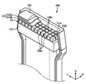
- FIG. 4 is a perspective view of an ultrasonic probe according to an exemplary embodiment.
- the ultrasonic probe 100 includes a piezoelectric layer 111, a sound absorbing layer 112 disposed under the piezoelectric layer 111, and a matching pattern disposed on the piezoelectric layer 111.
- a layer 113 and a lens layer 119 disposed on the matching layer 113 are included.
- it includes at least one cuff 118a, 118b formed in the piezoelectric layer 111 to divide the piezoelectric layer 111 into a plurality of piezoelectric elements.
- the cuffs 118a and 118b refer to spaces formed by a dicing process in which the piezoelectric layer 111 is divided into a plurality of piezoelectric elements 111a.
- the first cuff 118a may be formed between the plurality of piezoelectric elements 111a along the lateral direction L of the ultrasonic probe 100.
- the second cuff 118b may be formed between the plurality of piezoelectric elements 111a along the elevation direction E of the transducer module 110.
- the ultrasonic probe 100 forms a plurality of rows. It can be done, and a multi-row array arrangement can be formed.
- a first cuff 118a is formed between the plurality of piezoelectric elements 111a along the lateral direction L of the ultrasonic probe 100, and a plurality of piezoelectric elements 111a are formed along the elevation direction E of the ultrasonic probe 100.
- the ultrasonic probe 100 may form a multidimensional transducer array array, and may form a two-dimensional MXN matrix array. have.
- the ultrasonic probe 100 may describe each cross-section based on three directions that form a right angle with respect to the inner center of the ultrasonic probe 100.
- FIG. 5 is a cross-sectional view of an ultrasonic probe in an axis direction and a lateral direction plane according to an exemplary embodiment
- FIG. 6 is a plane in an axis direction and an elevation direction of the ultrasonic probe according to an exemplary embodiment. It is a cross-sectional view of the top.
- the ultrasonic transducer module 110 includes the piezoelectric layer 111, the sound absorbing layer 112 and the piezoelectric layer 111 provided under the piezoelectric layer 111. It includes a matching layer 113 provided on the top.
- the piezoelectric layer 111 is made of a piezoelectric material (piezoelectric material) that generates ultrasonic waves by converting electrical signals into mechanical vibrations. Further, the piezoelectric body may be laminated in a single layer or multilayer structure.
- piezoelectric material When a mechanical pressure is applied to a predetermined material, a voltage is generated, and when a voltage is applied, a mechanical deformation occurs is referred to as a piezoelectric effect and a reverse piezoelectric effect, and a material having such an effect is called a piezoelectric material (piezoelectric material).
- piezoelectric material refers to a material that converts electrical energy into mechanical vibration energy and mechanical vibration energy into electrical energy.
- the piezoelectric material may include a ceramic of lead zirconate titanate (PZT), a PZMT single crystal made of a solid solution of lead magnesium niobate and lead titanate, or a PZNT single crystal made of a solid solution of lead zinc niobate and lead titanate.
- PZT lead zirconate titanate
- PZMT PZMT single crystal made of a solid solution of lead magnesium niobate and lead titanate
- a PZNT single crystal made of a solid solution of lead zinc niobate and lead titanate.
- the piezoelectric layer 111 may be processed in the form of a multidimensional array in the form of a matrix forming a plurality of columns by a dicing process. In this case, the piezoelectric layer 111 may be separated into a plurality of piezoelectric elements 111a by cuffs 118a and 118b.
- the sound-absorbing layer 112 is provided under the piezoelectric layer 111 and absorbs ultrasonic waves generated in the piezoelectric layer 111 and proceeding backward, thereby preventing the ultrasonic waves from proceeding to the rear of the piezoelectric layer 111. Accordingly, it is possible to prevent distortion of the image from occurring.
- the sound-absorbing layer 112 may have an acoustic impedance smaller than that of the piezoelectric layer 111.
- the sound-absorbing layer 112 may be made of a material having an acoustic impedance of 2MRayl to 5MRayl.
- the sound-absorbing layer 112 may be formed of a plurality of layers to improve the attenuation or blocking effect of ultrasonic waves.
- a matching layer 113 is provided on the piezoelectric layer 111.
- the matching layer 113 may include a first matching layer 113a and a second matching layer 113b.
- the first and second matching layers 113a and 113b are layers that transmit ultrasonic waves to the object or reduce loss of ultrasonic waves transmitted from the object by appropriately matching the acoustic impedance of the piezoelectric layer 111 with the acoustic impedance of the object.
- the acoustic impedance of the object and the piezoelectric layer 111 may be matched by adjusting physical parameters such as sound speed, thickness, and acoustic impedance of the first and second matching layers 113a and 113b.
- the first and second matching layers 113a and 113b suppress reflection of ultrasonic waves caused by a difference between the acoustic impedance of the object and the acoustic impedance of the piezoelectric layer 111.
- two matching layers are shown in FIG. 5, this embodiment is not limited to this.
- one layer of matching layers or three or more matching layers may be used.
- the first and second matching layers 113a and 113b may be separated into a plurality of devices and may be provided on the top of the piezoelectric layer 111.
- the matching layer 113 matches the acoustic impedance of the piezoelectric layer 111 and the object ob by reducing the difference in acoustic impedance between the piezoelectric layer 111 and the object ob. Make sure it is delivered efficiently with (ob).
- the matching layer 113 may be formed of a material that is smaller than the piezoelectric layer 111 and has an acoustic impedance greater than that of the object ob.
- the matching layer 113 may be formed of a glass or resin material.
- a plurality of matching layers 113 may be formed so that the acoustic impedance can be changed stepwise from the piezoelectric layer 111 toward the object ob, and the plurality of matching layers 113 may have different materials. I can.
- the matching layer 113 may be processed into a matrix-shaped multidimensional array or a one-dimensional array through a dicing process.
- the lens layer 119 may be provided to cover the upper portion of the matching layer 113.
- the lens layer 119 focuses ultrasonic waves traveling forward of the transducer module 110 layer to a specific point.
- the lens layer 119 focuses ultrasonic waves, and in order to protect the acoustic module, in particular, the piezoelectric layer 111, the lens layer 119 may be formed of a material having high ultrasonic propagation speed while having strong wear resistance. have.
- the lens layer 119 may have a convex shape in the radial direction of the ultrasound waves to focus the ultrasound, and may be implemented in a concave shape when the sound velocity is slower than the object ob.
- the ultrasonic transducer module 110 may further include a first circuit layer 114 and a second circuit layer 115 disposed between the piezoelectric layer 111 and the sound absorbing layer 112. have.
- the first circuit layer 114 and the second circuit layer 115 may include electrodes to which an electric signal may be applied.
- the first circuit layer 114 and the second circuit layer 115 may include at least one of a signal electrode receiving current (not shown) or a ground electrode emitting current (not shown).
- At least one of the first circuit layer 114 and the second circuit layer 115 may be implemented as a printed circuit board (PCB).
- PCB printed circuit board
- At least one of the first circuit layer 114 and the second circuit layer 115 may be implemented as a flexible printed circuit board (FPCB).
- FPCB flexible printed circuit board
- the second circuit layer 115 may be formed to be spaced apart from the first circuit layer 114, and may be formed to be spaced apart based on a predetermined interval.
- first circuit layer 114 and the second circuit layer 115 may be disposed between the first circuit layer 114 and the second circuit layer 115.
- an insulating layer 119 may be disposed between the first circuit layer 114 and the second circuit layer 115.
- the insulating layer 119 may prevent the first circuit layer 114 and the second circuit layer 115 from directly contacting each other. To this end, the insulating layer 119 may be made of a non-conductive material.
- the insulating layer 119 may be formed using an epoxy resin. Since the epoxy resin may provide an adhesive function, the first circuit layer 114 and the second circuit layer 115 may be adhered to each other by an insulating layer 119 made of an epoxy resin.
- the case in which the insulating layer 119 is disposed between the first circuit layer 114 and the second circuit layer 115 has been described as an example.
- the first circuit layer 114 and the second circuit layer The positions of the 115 and the insulating layer 119 are not limited to the above-described examples, and may be disposed at various positions.
- At least one or more circuit layers may be formed between the first circuit layer 114 and the second circuit layer 115.
- the ultrasonic probe 110 may further include an enhanced layer 117.
- the reflective layer 117 may reflect ultrasonic waves generated from the piezoelectric layer 111.
- the reflective layer 117 may be disposed under the piezoelectric layer 111, and may be formed in direct contact with or spaced apart from the piezoelectric layer 111. However, it is not limited to this example and may be disposed in various positions.
- the transducer module 110 may form at least one cuff 118a and 118b by a dicing process, and may include a plurality of piezoelectric elements 111a.
- the transducer module 110 may include a first cuff 118a formed between piezoelectric elements along the lateral direction L.
- the first cuff 118a may be formed regularly at predetermined intervals. However, it is not limited thereto, and may be formed at different intervals.
- the first cuff 118a is not only the piezoelectric layer 111 but also the matching layer 113, the first circuit layer 114, the second circuit layer 115, the reflective layer 117, or the insulating layer 119 It may be formed to separate at least one.
- the first cuff 118a is a matching layer 113, a first circuit layer 114, a second circuit layer 115, a reflective layer 117, or an insulating layer 119 from the top of the piezoelectric element 111a. It may be formed to extend to any one of the specific positions.
- the first cuff 118a may be formed to extend from the upper surface of the piezoelectric layer 111 to the sound absorbing layer 112.
- the first cuff 118a may be formed by extending from the upper surface of the piezoelectric layer 111 to a first position inside the sound absorbing layer 112, and the first position is predetermined with respect to the inside of the sound absorbing layer 112 It can be set to a position with depth. In this case, the first cuff 118a does not penetrate the sound absorbing layer 112 and forms a space inside the sound absorbing layer 112.
- the transducer module 110 may include a second cuff 118b formed between piezoelectric elements along the elevation direction E.
- the second cuff 118b may be regularly formed at predetermined intervals. However, it is not limited thereto, and may be formed at different intervals.
- the second cuff 118b is not only the piezoelectric layer 111 but also the matching layer 113, the first circuit layer 114, the second circuit layer 115, the reflective layer 117, or the insulating layer 119 It may be formed to separate at least one.
- the second cuff 118b includes a matching layer 113, a first circuit layer 114, a second circuit layer 115, a reflective layer 117, or an insulating layer 119 from the top of the piezoelectric element 111a. It may be formed to extend to any one of the specific positions.
- the second cuff 118b may be formed to extend from the top surface of the piezoelectric layer 111 to the top of the first circuit layer 114. Specifically, the second cuff 118b may be formed to extend from the upper surface of the piezoelectric layer 111 to a second position above the sound-absorbing layer 112, and the second position is with respect to the first circuit layer 114 It can be set to a position having a predetermined height. In this case, unlike the first cuff 118a, the second cuff 118b is not formed to the inside of the sound-absorbing layer 112, and thus electrical disconnection (open) can be prevented.
- FIG. 7 is a cross-sectional view illustrating a lateral direction of an ultrasonic probe according to an exemplary embodiment
- FIG. 8 is a diagram illustrating a connection part according to an exemplary embodiment.
- the ultrasonic probe 100 includes a piezoelectric layer 111, a sound absorbing layer 112 provided under the piezoelectric layer 111, and an upper portion of the piezoelectric layer 111.
- the connection part 116 may include a via hole 116-3.
- the connection part 116 may be formed by a process for forming the via hole 116-3, and the via hole 116-3 includes a laser via drilling process or an etching process. It can be formed in a variety of processes.
- connection part 116 electrically connects the first circuit layer 114 and the second circuit layer 115 by at least one of conductive paste, conductive plating, sputtering, and printing. I can. However, it is not limited to the above-described example, and the first circuit layer 114 and the second circuit layer 115 may be electrically connected by various connection methods.
- the via hole 116-3 may be implemented as a conductive hole.
- the via hole 116-3 may be implemented as a conductive hole by plating or processing with a conductive material such as gold, silver, or copper, but is not limited to the above-described example.
- connection part 116 may be formed to extend from the first circuit layer 114 to the second circuit layer 115.
- connection part 116 may be formed to penetrate the first circuit layer 114 and the second circuit layer 115.
- the via hole 116-3 may be implemented in the form of a through-hole.
- connection part 116 may be formed to penetrate only one of the first circuit layer 114 or the second circuit layer 115.
- the via hole 116-3 may be implemented in the form of a blind-hole.
- connection part 116 may be formed so that the inside of the via hole is filled with a predetermined amount of a conductive material.
- the via hole 116-3 may be implemented in the form of a filled-via.
- connection part 116 may be formed to connect the circuit patterns P1 and P2 made of conductive wires formed on the first circuit layer 114 and the second circuit layer 115.
- a via hole 116-3 connecting the first circuit layer 114 and the second circuit layer 115 may be included.
- connection part 116 may electrically connect the first circuit layer 114 and the second circuit layer 115. To this end, the connection part 116 may contact the first circuit layer 114 and the second circuit layer 115 at both ends.
- connection part 116 is connected to the first circuit pattern P1 formed on the first circuit layer 114 and the second circuit pattern P2 formed on the second circuit layer 115, so that the first circuit layer 114 ) And the second circuit layer 115 at both ends.
- each of the first circuit pattern P1 and the second circuit pattern P2 may include an electrode and may be implemented with a conductive material such as copper.
- the first circuit pattern P1 and the second circuit pattern P2 may have various shapes or shapes for wiring in addition to the embodiment shown in FIG. 8.
- the connection part 116 may include a first board connection part 116-1 located on the first circuit pattern P1 and a second board connection part 116-2 located on the second circuit pattern P2.
- the connection part 116 may contact the first circuit layer 114 through the first board connection part 116-1, and the second circuit layer 115 through the second board connection part 116-2. I can.
- the first substrate connection part 116-1 may be formed to have the same size as the via hole 116-3.
- the present invention is not limited thereto, and may be formed to have a size larger or smaller than the via hole 116-3.
- the first substrate connection part 116-1 may have a circular shape when viewed from a vertical upward direction of the first circuit layer 114. Depending on the embodiment, the first substrate connection part 116-1 may have a polygonal shape such as a triangle or a square, or may have a shape such as an ellipse.
- the first substrate connection portion 116-1 may be formed on the first circuit layer 114 by drilling the first circuit layer 114 using a drilling device such as a drill tool.
- the second substrate connection part 116-2 may be formed to have a larger size than the via hole 116-3. That is, the diameter of the second substrate connection portion 116-2 may be larger than the diameter of the via hole 116-3. In this case, when the first substrate connection portion 116-1 is formed to have the same size as the via hole 116-3, the second substrate connection portion 116-2 is less than the diameter of the first substrate connection portion 116-1. It can be formed to have a large diameter. However, the size of the second substrate connection portion 116-2 is not limited to the above-described example, and may be formed to have the same size as the via hole 116-3 or a small size.
- the second substrate connection portion 116-2 may have a circular shape when viewed from the vertical upper direction of the second circuit layer 114.
- the second substrate connection portion 116-2 may have a polygonal shape such as a triangle or a square, or may have a shape such as an ellipse.
- the second substrate connection portion 116-2 may be formed on the second circuit layer 115 by drilling the second circuit layer 115 using a drilling device such as a drill tool.
- FIG. 9 is a view showing an interior view of a conventional ultrasonic probe as viewed from an axis direction.
- the first circuit pattern P1' and the second circuit pattern P2' for forming the via hole 116' are the transducer module 111a'. It is formed in consideration of the size of. That is, the first circuit pattern P1 ′ and the second circuit pattern P2 ′ for forming the via hole 116 ′ are located inside a region corresponding to the size of each of the transducer modules 111a ′.
- the via hole 116 ′ of the conventional ultrasonic probe is formed in consideration of the size of the transducer module 111a ′. That is, the conventional via hole 116 ′ is also formed to be located inside a region corresponding to the size of the transducer module 111a ′.
- the design range for the first circuit pattern P1' and the second circuit pattern P2' in consideration of the size of the transducer module 111a' is that the number of rows increases or the transducer module 111a' If the size of) is reduced, the difficulty of dicing increases, and the cost and defect rate may increase.
- FIG. 10 is a cross-sectional view of an ultrasonic probe in an axis direction and a lateral direction plane according to an exemplary embodiment.
- the ultrasonic transducer module 110 is provided on the piezoelectric layer 111, the sound absorbing layer 112 provided under the piezoelectric layer 111, and the piezoelectric layer 111
- the matching layer 113, the piezoelectric layer 111, and the sound-absorbing layer 112 are included in the first circuit layer 114, the second circuit layer 115, the reflective layer 117, and the insulating layer 119.
- a connection part 116 electrically connecting the first cuff 118a formed between the piezoelectric elements along the lateral direction and the first circuit layer 114 and the second circuit layer 115 Can include.
- connection part 116 may have a width greater than that of the first cuff 118a. That is, the width Wk of the first cuff 118a may have a value smaller than the widths W1 and W2 of the connection part 116.
- connection part 116 Since the connection part 116 is formed to have a width greater than the width of the first cuff 118a, the first cuff 118a may be formed inside the connection part 116. In other words, the connection part 116 may be separated by the first cuff 118a, and may be separated by a dicing process for forming the first cuff 118a.
- the widths W1 and W2 of the connection part 116 may be formed to have different values, and both may have a width greater than the width Wk of the first cuff 118a. However, it is not limited to the above-described example, and the widths W1 and W2 of the connection part 116 may be formed to have the same predetermined value.
- the ultrasonic probe 100 since the ultrasonic probe 100 according to an embodiment can form the connection portion 116 arranged regardless of the size of the piezoelectric element 111a, design and manufacture even if the number of rows increases in the multi-row probe. Convenience can be increased. At the same time, manufacturing costs can also be lowered. That is, since a design that is not sensitive to the size of the piezoelectric element 111a and the number of rows is possible, a high specification multi-row probe can be implemented.
- the first cuff 118a formed between the piezoelectric elements along the lateral direction may be formed to extend from the top surface of the piezoelectric layer 111 to a first position inside the sound absorbing layer 112.
- the first cuff 118a may be formed to extend from the top surface of the piezoelectric layer 111 to at least one of the first circuit layer 114 or the second circuit layer 115.
- the second cuff 118b formed between the piezoelectric elements along the elevation direction may be formed to extend from the upper surface of the piezoelectric layer 111 to a second position above the first circuit layer 114.
- the second cuff 118b may be formed by extending from the upper surface of the piezoelectric layer 111 to a third position above the second circuit layer 115.
- the second cuff 118b may be formed not to be located inside the sound-absorbing layer 112. In this case, unlike the first cuff 118a, the second cuff 118b does not form a space inside the sound-absorbing layer 112, and thus electrical disconnection (open) can be prevented.
- FIG. 11A is a view showing an interior view as viewed from the axis direction of the ultrasonic probe according to an exemplary embodiment
- FIG. 11B is a diagram illustrating an axis direction of the ultrasonic probe in which the piezoelectric layer of FIG. 11A is diced. It is a drawing showing the view of the inside.
- the ultrasonic probe 100 includes a first cuff 118a formed between a plurality of piezoelectric elements (described as 111a and 11b for convenience) along a lateral direction. Includes.
- connection part 116 may have a width greater than that of the first cuff 118a. That is, the width Wk of the first cuff 118a may have a value smaller than the widths Wa and Wb of the connection part 116.
- the via hole 116-3 of the connection portion 116 is the second pattern P2 of the second circuit layer 115 It may be formed on the second substrate connection part 116-2 connected to the.
- the first cuff 118a may be formed to have a width smaller than or equal to the width Wa of the via hole 116-3.
- the width (Wa) of the via hole (116-3) may be the diameter of the via hole (116-3), and the diameter (Wa) of the via hole (116-3) is the width (Wk) of the first cuff (118a) It can be formed to have a value greater than or equal to.
- first cuff 118a may be formed to have a width smaller than the width Wb of the second substrate connection portion 116-2.
- the width Wb of the second substrate connection portion 116-2 may be the diameter of the second substrate connection portion 116-2, and the diameter Wb of the second substrate connection portion 116-2 is the first cuff 118a ) May be formed to have a larger value than the width Wk.
- connection portion 116 including the via hole 116-3 formed on the second substrate connection portion 116-2 is formed to have a width greater than the width Wk of the first cuff 118a, the first cuff (118a) may be formed inside the connection portion 116.
- connection part 116 may be separated by the first cuff 118a and may be separated by a dicing process for forming the first cuff 118a.
- connection part 116 may be formed to be symmetrical with respect to the first cuff 118a. Specifically, the connection part 116 may be formed to have a symmetrical size in left and right about the center of the first cuff 118a in a lateral direction. That is, the size of at least one of the via hole 116-3 or the second substrate connection portion 116-2 separated by the first cuff 118a may be the same.
- connection part 116 may be separated asymmetrically around the first cuff 118a. Further, in the connection part 116, both the via hole 116-3 and the second substrate connection part 116-2 are separated by the first cuff 118a, or the via hole 116-3 is not separated and the second substrate Only the connection portion 116-2 may be separated.
- FIG. 12A is a perspective view of a connection portion separated by a first cuff of an ultrasonic probe according to an embodiment
- FIG. 12B is a cross-sectional view of a connection portion viewed in a lateral direction of the ultrasonic probe according to an embodiment.
- connection part 116 of the ultrasonic probe 100 includes a first substrate connection part 116-1 connected to the first circuit layer 114, and a first circuit layer ( 114) and a via hole 116-3 electrically connecting the second circuit layer 115 and a second substrate connecting portion 116-2 connected to the second circuit layer 114.
- An insulating part 119 may be disposed between the first circuit layer 114 and the second circuit layer 115, and the connection part 116 connects the first circuit layer 114 and the second circuit layer 115 to each other.
- a via hole 116-3 may be included therethrough.
- At least one of the first and second substrate connections 116-1 and 116-2 may be provided to contact one surface of each of the first circuit layer 114 or the second circuit layer 115.
- the first and second substrate connections 116-1 and 116-2 may be formed by applying a conductive material such as copper to the inner side of the via hole 116-3.
- a conductive material such as copper
- the opening of the via hole 116-3 is connected to one surface of the first circuit layer 114 or the second circuit layer 115 It may be formed to extend to contact.
- connection portion 116 separated by the first cuff 118a formed along the lateral direction may be formed in a semicircular shape. That is, at least one of the first substrate connection portion 116-1, the second substrate connection portion 116-2, and the via hole 116-3 may be separated to have a semicircular shape.
- the shape of the conductive material M inside the via hole 116-3 is also a semicircle. It can be separated as much as possible.
- connection part 116 separated by the first cuff 118a is not limited to a semicircle, and when the polygonal connection part 116 is separated by the first cuff 118a, it is separated to have a polygonal shape. Can be.
- the first cuff 118a may be formed to separate both the second substrate connection portion 116-2 and the via hole 116-3, and according to the embodiment, the first cuff 118a The 118a may be formed to separate only the second substrate connection portion 116-2 without separating the via hole 116-3. That is, the first cuff 118a may be formed between the via hole 116-3 and the second substrate connection portion 116-2.
- FIG. 13A is a view showing an interior view of the ultrasonic probe in the direction of the axis of the ultrasonic probe according to another exemplary embodiment
- FIG. 13B is a view of the ultrasonic probe in which the piezoelectric layer of FIG. 13A is diced. It is a drawing showing the view of the inside.
- the ultrasonic probe 100 includes a first cuff 118a formed between a plurality of piezoelectric elements 111a and 111b along a lateral direction.
- the via of the connection part 116 may be formed on the second substrate connection part 116-2 connected to the second pattern P2 of the second circuit layer 115.
- connection part 116 of the ultrasonic probe 100 in the connection part 116 of the ultrasonic probe 100 according to an embodiment, the via hole 116-3 is not separated by the first cuff 118a, Only the second substrate connection portion 116-2 may be formed to be separated by the first cuff 118a.
- the first cuff 118a may be formed to be positioned outside the via hole 116-3 and inside the second substrate connection portion 116-2, and the width Wk of the first cuff 118a is It may be smaller than the width of the second substrate connection part 116-2.
- the first is located outside the via hole 116-3 and inside the second substrate connection portion 116-2, that is, in a region where the via hole 116-3 is not located among the regions of the second substrate connection portion 116-2.
- the connecting portion 116 separated around the first cuff 118a may have an asymmetric shape.
- connection portion 116 is the first piezoelectric element 111a.
- Both the via hole 116-3 and the second substrate connection 116-2 are included on the side, and the via hole 116-3 and the second substrate connection 116-2 are both on the second piezoelectric element 111b side. It can be divided so that it does not contain.
- connection part 116 includes both the via hole 116-3 and the second substrate connection part 116-2 at the side of the first piezoelectric element 111a, and the second substrate connection part at the side of the second piezoelectric element 111b ( 116-2) can be divided.
- 14 to 16 are diagrams illustrating an interior view of an ultrasonic probe from an axis direction according to various embodiments.
- the ultrasonic probe 100 includes a first cuff 118a formed between a plurality of piezoelectric elements (described as 111a and 11b for convenience) along a lateral direction. Includes.
- connection part 116 when viewed from the vertical upper direction of the piezoelectric elements 111a and 111b, the via hole 116-3 of the connection part 116 is a second substrate connected to the second pattern P2 of the second circuit layer 115 It may be formed on the connection part 116-2.
- the second pattern P2 of the second circuit layer 115 may be formed to have various shapes, and may be formed to have a wiring structure for at least one piezoelectric element through the via hole 116-3.
- the second pattern P2 connects the piezoelectric elements located in the second and fourth columns, and ,
- the piezoelectric elements positioned in the first and fifth columns are connected, and the piezoelectric elements positioned in the third column may be formed to have separate wirings.
- the second pattern P2 since the second pattern P2 includes a conductive wiring having a mass, it may be formed to have different masses according to the wiring structure.
- the second pattern P2 has the same weight in the left and right directions with respect to the central axis of the transducer module 110 (in the case of the embodiment of FIG. 14, the central axis of the piezoelectric elements located in the third row) or the central axis. It may be formed to reduce the difference in weight in the left and right directions as a reference.
- the second pattern P2 may be formed such that the number of portions X where the conductive wire is cut is the same in the horizontal direction based on the central axis of the transducer module 110. have.
- the second pattern P2 may be formed to include a wiring that is not connected to any piezoelectric element, that is, a dummy wiring Pd that is not connected to the second substrate connection portion 116-2.
- the second pattern P2 may be formed so that the weight of the wiring connected to the second substrate connection part 116-2 is the same in the left and right direction with respect to the central axis of the transducer module 110. .
- the second pattern P2 may be formed to include a wire connected to at least one second substrate connection part 116-2. That is, the second pattern P2 may be formed so as not to include a wiring (Pd in FIG. 14) that is not connected to any piezoelectric element.
- the second pattern P2 may be formed to minimize a portion (X in FIG. 14) where the conductive wire is cut.
- the second pattern P2 may be formed such that the weight including the weight of the wires bent in the left and right directions with respect to the central axis of the transducer module 110 is the same.
- the above description can be applied not only to the second pattern P2 but also to the first pattern P1 in which the via hole 116-1 is located, and the weight of the first pattern P1 is also applied to the center of the transducer module 110. It can be the same in the left and right directions based on the axis.
- the first pattern P1 or the second pattern P2 may be formed so that the weight in the left and right directions is the same with respect to the central axis of the transducer module 110. Therefore, it is possible to minimize the influence of the vibration characteristics of the piezoelectric element 111a. Accordingly, a higher quality image can be output and reliability can be increased.
- 17 is a flowchart illustrating a method of manufacturing an ultrasonic probe according to an exemplary embodiment.
- a sound absorbing layer 112 may be provided (710 ).
- a second circuit layer 115 covering the upper portion of the sound-absorbing layer 112 may be provided (720 ).
- the second circuit layer 115 may be provided to form a second pattern P2 having a predetermined wiring structure.
- the second pattern P2 may include an electrode, and may be implemented with a conductive material such as copper.
- the second pattern P2 may be formed to have various shapes for wiring, and may be formed to have a wiring structure for at least one piezoelectric element through the via hole 116-3.
- the second pattern P2 may be formed to have the same weight in the left and right directions based on the central axis of the transducer module 110.
- the first circuit layer 114 may be provided (730).
- the first circuit layer 114 may be formed to be spaced apart from the second circuit layer 115.
- an insulating layer 119 covering an upper portion of the second circuit layer 115 may be provided or at least one or more circuit layers having different physical properties may be provided, and then the first circuit layer 114 may be provided.
- the first circuit layer 114 may be provided to form a first pattern P1 having a predetermined wiring structure.
- the second pattern P2 may include an electrode, and may be implemented with a conductive material such as copper.
- the first pattern P1 may be formed to have various shapes for wiring, and may be formed to have a wiring structure for at least one piezoelectric element through the via hole 116-3. Specifically, the first pattern P1 may be formed to have the same weight in the left and right directions based on the central axis of the transducer module 110.
- connection part 116 connecting the first circuit layer 114 and the second circuit layer 115 may be provided (740).
- the connection part 116 may include a via hole 116-3.
- the connection part 116 may be formed by a process for forming the via hole 116-3, and the via hole 116-3 includes a laser via drilling process or an etching process. It can be formed in a variety of processes.
- connection part 116 electrically connects the first circuit layer 114 and the second circuit layer 115 by at least one of conductive paste, conductive plating, sputtering, and printing. I can. However, it is not limited to the above-described example, and the first circuit layer 114 and the second circuit layer 115 may be electrically connected by various connection methods.
- the via hole 116-3 may be implemented as a conductive hole.
- the via hole 116-3 may be implemented as a conductive hole by plating or processing with a conductive material such as gold, silver, or copper, but is not limited to the above-described example.
- connection part 116 may be formed to extend from the first circuit layer 114 to the second circuit layer 115.
- connection part 116 may be formed to penetrate the first circuit layer 114 and the second circuit layer 115.
- the via hole 116-3 may be implemented in the form of a through-hole.
- connection part 116 may be formed to penetrate only one of the first circuit layer 114 or the second circuit layer 115.
- the via hole 116-3 may be implemented in the form of a blind-hole.
- connection part 116 may be formed so that the inside of the via hole is filled with a predetermined amount of a conductive material.
- the via hole 116-3 may be implemented in the form of a filled-via.
- connection part 116 may electrically connect the first circuit layer 114 and the second circuit layer 115 by making contact with the first circuit layer 114 and the second circuit layer 115 at both ends.
- connection part 116 is connected to the first circuit pattern P1 formed on the first circuit layer 114 and the second circuit pattern P2 formed on the second circuit layer 115, so that the first circuit layer 114 ) And the second circuit layer 115 at both ends.
- the connection part 116 may include a first board connection part 116-1 located on the first circuit pattern P1 and a second board connection part 116-2 located on the second circuit pattern P2.
- the connection part 116 may contact the first circuit layer 114 through the first board connection part 116-1, and the second circuit layer 115 through the second board connection part 116-2. I can.
- the first substrate connection part 116-1 may be formed to have the same size as the via hole 116-3.
- the present invention is not limited thereto, and may be formed to have a larger size than the via hole 116-3 or may be formed to have a different size.
- the first substrate connection part 116-1 may have a circular shape when viewed from a vertical upward direction of the first circuit layer 114. Depending on the embodiment, the first substrate connection part 116-1 may have a polygonal shape such as a triangle or a square, or may have a shape such as an ellipse.
- the first substrate connection portion 116-1 may be formed on the first circuit layer 114 by drilling the first circuit layer 114 using a drilling device such as a drill tool.
- the second substrate connection part 116-2 may be formed to have a larger size than the via hole 116-3. That is, the diameter of the second substrate connection portion 116-2 may be larger than the diameter of the via hole 116-3. In this case, when the first substrate connection portion 116-1 is formed to have the same size as the via hole 116-3, the second substrate connection portion 116-2 is less than the diameter of the first substrate connection portion 116-1. It can be formed to have a large diameter.
- the size of the second substrate connection part 116-2 is not limited to the above-described example, and may be formed to have the same size as the via hole 116-3 or a different size.
- the second substrate connection portion 116-2 may have a circular shape when viewed from the vertical upper direction of the second circuit layer 114.
- the second substrate connection portion 116-2 may have a polygonal shape such as a triangle or a square, or may have a shape such as an ellipse.
- the second substrate connection portion 116-2 may be formed on the second circuit layer 115 by drilling the second circuit layer 115 using a drilling device such as a drill tool.
- the piezoelectric layer 111 may be provided (750 ).
- the piezoelectric layer 111 is made of a piezoelectric material (piezoelectric material) that generates ultrasonic waves by converting electrical signals into mechanical vibrations. Further, the piezoelectric body may be laminated in a single layer or multilayer structure.
- the piezoelectric layer 111 may be provided on the upper surface of the first circuit layer 114, and may be provided on the upper surface of the reflective layer 117 when the reflective layer 117 is provided on the upper surface of the first circuit layer 114.
- a matching layer 113 covering an upper portion of the piezoelectric layer 111 may be provided (760).
- the matching layer 113 is a layer that appropriately matches the acoustic impedance of the piezoelectric layer 111 and the acoustic impedance of the object to transmit ultrasonic waves to the object or to reduce loss of ultrasonic waves transmitted from the object.
- the matching layer 113 may be provided in a single layer or multilayer structure.
- a dicing process of dividing the piezoelectric layer 111 into a plurality of piezoelectric elements 111a may be performed (770).
- the piezoelectric layer 111 may be divided into a plurality of piezoelectric elements forming a multi-row array arrangement by the generated cuffs 118a and 118b.
- the piezoelectric layer 111 may be divided into a plurality of piezoelectric elements 111a forming a plurality of rows in a lateral direction or an elevation direction.
- the first cuff 118a may be formed by extending from the upper surface of the piezoelectric layer 111 to the sound absorbing layer 112.
- the first cuff 118a may be formed by extending from the upper surface of the piezoelectric layer 111 to a first position inside the sound absorbing layer 112, and the first position is predetermined with respect to the inside of the sound absorbing layer 112 It can be set to a position with depth. In this case, the first cuff 118a does not penetrate the sound absorbing layer 112 and forms a space inside the sound absorbing layer 112.
- the second cuff 118b may be formed to extend from an upper surface of the piezoelectric layer 111 to an upper portion of the first circuit layer 114 or the second circuit layer 115. Specifically, the second cuff 118b may be formed to extend from the upper surface of the piezoelectric layer 111 to a second position above the sound absorbing layer 112, and the second position is predetermined with respect to the upper part of the sound absorbing layer 112. It can be set to a position with a height. In this case, unlike the first cuff 118a, the second cuff 118b does not form a space inside the sound-absorbing layer 112, and thus electrical disconnection (open) can be prevented.
- connection part 116 may be located in a dicing line for a dicing process, and in this case, the connection part 116 may be separated by a dicing process.
- connection part 116 may have a width greater than that of the first cuff 118a. That is, the width Wk of the first cuff 118a may have a value smaller than the width of the connection part 116. In this case, since the connecting portion 116 is formed to have a width greater than the width of the first cuff 118a, the first cuff 118a may be formed inside the connecting portion 116.
- the first cuff 118a may be formed to have a width smaller than or equal to the width Wa of the via hole 116-3.
- the width (Wa) of the via hole (116-3) may be the diameter of the via hole (116-3), and the diameter (Wa) of the via hole (116-3) is the width (Wk) of the first cuff (118a) It can be formed to have a value greater than or equal to.
- first cuff 118a may be formed to have a width smaller than the width Wb of the second substrate connection portion 116-2.
- the width Wb of the second substrate connection portion 116-2 may be the diameter of the second substrate connection portion 116-2, and the diameter Wb of the second substrate connection portion 116-2 is the first cuff 118a ) May be formed to have a larger value than the width Wk.
- connection part 116 may be formed to be symmetrical with respect to the first cuff 118a. Specifically, the connection part 116 may be formed to have a symmetrical size in left and right about the center of the first cuff 118a in a lateral direction. That is, the size of at least one of the via hole 116-3 or the second substrate connection portion 116-2 separated by the first cuff 118a may be the same.
- connection part 116 may be separated asymmetrically around the first cuff 118a.
- both the via hole 116-3 and the second substrate connection part 116-2 are separated by the first cuff 118a, or the via hole 116-3 is not separated and 2 Only the substrate connection part 116-2 may be separated.
- the first cuff 118a may be formed to be positioned outside the via hole 116-3 and inside the second substrate connection portion 116-2, and the width Wk of the first cuff 118a is It may be smaller than the width of the second substrate connection part 116-2.
- the first is located outside the via hole 116-3 and inside the second substrate connection portion 116-2, that is, in a region where the via hole 116-3 is not located among the regions of the second substrate connection portion 116-2.
- the connecting portion 116 separated around the first cuff 118a may have an asymmetric shape.
- connection portion 116 is a via hole 116-3 on the side of the first piezoelectric element 111a.
- the second substrate connection part 116-2, and the via hole 116-3 and the second substrate connection part 116-2 may not be included at the side of the second piezoelectric element 111b.
- connection part 116 includes both the via hole 116-3 and the second substrate connection part 116-2 at the side of the first piezoelectric element 111a, and the second substrate connection part at the side of the second piezoelectric element 111b ( 116-2) can be divided.
- a lens layer 119 covering an upper portion of the matching layer 113 may be provided (780 ).
- the lens layer 119 may be formed of a material having strong abrasion resistance and a high ultrasonic propagation speed in order to focus ultrasonic waves and protect the piezoelectric layer 111.
- the lens layer 119 may have a convex shape in the radial direction of the ultrasound waves to focus the ultrasound, and may be implemented in a concave shape when the sound velocity is slower than the object ob.
- the method of manufacturing the ultrasonic probe 100 may provide the connection portion 116 disposed regardless of the size of the piezoelectric element 111a, and a dicing process for separating the connection portion 116 is performed. Therefore, even if the number of rows increases in the multi-row probe, the convenience of design and manufacture can be increased. At the same time, the difficulty of dicing may be lowered, and at the same time, design cost and manufacturing cost may also be lowered. That is, since a design that is not sensitive to the size of the piezoelectric element 111a and the number of rows is possible, a high specification multi-row probe can be implemented.
- FIG. 17 illustrates a process of dividing the piezoelectric layer 111 into 770 after preparing the matching layer 117 (760), but after the piezoelectric layer 111 is divided (770), the matching layer 117 ) May be provided (760).
- FIG. 17 shows that after the second circuit layer is provided (720), the first circuit layer is provided (710), and the connection portion 114 is provided (740), the order of formation of each layer is reversed. It is possible. In addition, steps 720, 730, and 740 may be performed simultaneously, and the order is not limited to the above-described example.
- the piezoelectric layer 111 may be divided through a dicing process to form a plurality of elements.
- the piezoelectric layer 111 may be divided through a dicing process to form a plurality of elements.
- it can be formed by stacking the diced piezoelectric material or elements.
- the structure of the piezoelectric layer and the plurality of cuffs in FIGS. 4 to 17 are examples, and there may be more multilayer structures, and more cuffs may be formed. Accordingly, a single or a plurality of elements may also be formed to have various thicknesses and widths.
- the disclosed embodiments may be implemented in the form of a recording medium storing instructions executable by a computer.
- the instruction may be stored in the form of a program code, and when executed by a processor, a program module may be generated to perform the operation of the disclosed embodiments.
- the recording medium may be implemented as a computer-readable recording medium.
- Computer-readable recording media include all kinds of recording media in which instructions that can be read by a computer are stored. For example, there may be read only memory (ROM), random access memory (RAM), magnetic tape, magnetic disk, flash memory, optical data storage device, and the like.
- ROM read only memory
- RAM random access memory
- magnetic tape magnetic tape
- magnetic disk magnetic disk
- flash memory optical data storage device
Landscapes
- Health & Medical Sciences (AREA)
- Life Sciences & Earth Sciences (AREA)
- Engineering & Computer Science (AREA)
- Medical Informatics (AREA)
- Biophysics (AREA)
- Nuclear Medicine, Radiotherapy & Molecular Imaging (AREA)
- Pathology (AREA)
- Radiology & Medical Imaging (AREA)
- Veterinary Medicine (AREA)
- Biomedical Technology (AREA)
- Heart & Thoracic Surgery (AREA)
- Physics & Mathematics (AREA)
- Molecular Biology (AREA)
- Surgery (AREA)
- Animal Behavior & Ethology (AREA)
- General Health & Medical Sciences (AREA)
- Public Health (AREA)
- Gynecology & Obstetrics (AREA)
- Ultra Sonic Daignosis Equipment (AREA)
Abstract
Une sonde ultrasonore, selon un mode de réalisation de la présente invention, comprend : des éléments piézoélectriques qui forment une pluralité de rangées le long d'une direction d'élévation ; une première entaille formée entre les éléments piézoélectriques le long d'une direction latérale ; une couche d'adaptation disposée au-dessus des éléments piézoélectriques ; une couche d'absorption sonore disposée au-dessous des éléments piézoélectriques ; une première couche de circuit disposée entre la couche d'adaptation et la couche d'absorption sonore ; une deuxième couche de circuit formée de façon espacée de la première couche de circuit ; et une partie de connexion pour connecter électriquement la première couche de circuit et la deuxième couche de circuit, et ayant une largeur supérieure à celle de la première entaille.
Applications Claiming Priority (2)
| Application Number | Priority Date | Filing Date | Title |
|---|---|---|---|
| KR1020190027548A KR20200108642A (ko) | 2019-03-11 | 2019-03-11 | 초음파 프로브 및 그 제조 방법 |
| KR10-2019-0027548 | 2019-03-11 |
Publications (1)
| Publication Number | Publication Date |
|---|---|
| WO2020184830A1 true WO2020184830A1 (fr) | 2020-09-17 |
Family
ID=72427427
Family Applications (1)
| Application Number | Title | Priority Date | Filing Date |
|---|---|---|---|
| PCT/KR2020/000617 Ceased WO2020184830A1 (fr) | 2019-03-11 | 2020-01-13 | Sonde ultrasonore et son procédé de fabrication |
Country Status (2)
| Country | Link |
|---|---|
| KR (1) | KR20200108642A (fr) |
| WO (1) | WO2020184830A1 (fr) |
Families Citing this family (3)
| Publication number | Priority date | Publication date | Assignee | Title |
|---|---|---|---|---|
| KR102802030B1 (ko) * | 2020-04-22 | 2025-05-02 | 삼성메디슨 주식회사 | 초음파 프로브 |
| KR102623559B1 (ko) * | 2021-02-10 | 2024-01-11 | 주식회사 에프씨유 | 초음파 프로브 |
| KR20250039020A (ko) * | 2023-09-13 | 2025-03-20 | 알피니언메디칼시스템 주식회사 | 초음파 프로브 |
Citations (5)
| Publication number | Priority date | Publication date | Assignee | Title |
|---|---|---|---|---|
| US5744898A (en) * | 1992-05-14 | 1998-04-28 | Duke University | Ultrasound transducer array with transmitter/receiver integrated circuitry |
| KR20160086709A (ko) * | 2015-01-12 | 2016-07-20 | 삼성메디슨 주식회사 | 정합 부재 및 이를 포함한 초음파 프로브 |
| KR20170087632A (ko) * | 2016-01-21 | 2017-07-31 | 삼성메디슨 주식회사 | 초음파 프로브 및 초음파 프로브의 제조 방법 |
| JP2017158630A (ja) * | 2016-03-07 | 2017-09-14 | 東芝メディカルシステムズ株式会社 | 超音波プローブ |
| KR20180096298A (ko) * | 2017-02-21 | 2018-08-29 | 삼성메디슨 주식회사 | 초음파 프로브 |
-
2019
- 2019-03-11 KR KR1020190027548A patent/KR20200108642A/ko not_active Withdrawn
-
2020
- 2020-01-13 WO PCT/KR2020/000617 patent/WO2020184830A1/fr not_active Ceased
Patent Citations (5)
| Publication number | Priority date | Publication date | Assignee | Title |
|---|---|---|---|---|
| US5744898A (en) * | 1992-05-14 | 1998-04-28 | Duke University | Ultrasound transducer array with transmitter/receiver integrated circuitry |
| KR20160086709A (ko) * | 2015-01-12 | 2016-07-20 | 삼성메디슨 주식회사 | 정합 부재 및 이를 포함한 초음파 프로브 |
| KR20170087632A (ko) * | 2016-01-21 | 2017-07-31 | 삼성메디슨 주식회사 | 초음파 프로브 및 초음파 프로브의 제조 방법 |
| JP2017158630A (ja) * | 2016-03-07 | 2017-09-14 | 東芝メディカルシステムズ株式会社 | 超音波プローブ |
| KR20180096298A (ko) * | 2017-02-21 | 2018-08-29 | 삼성메디슨 주식회사 | 초음파 프로브 |
Also Published As
| Publication number | Publication date |
|---|---|
| KR20200108642A (ko) | 2020-09-21 |
Similar Documents
| Publication | Publication Date | Title |
|---|---|---|
| WO2017065562A1 (fr) | Appareil à sonde, instrument médical le comprenant et procédé de commande d'appareil à sonde | |
| WO2020184830A1 (fr) | Sonde ultrasonore et son procédé de fabrication | |
| US8547799B2 (en) | Ultrasonic probe, ultrasonic imaging apparatus and fabricating method thereof | |
| WO2015102474A1 (fr) | Appareil de diagnostic à ultrasons, procédé de capture d'image à ultrasons et support d'enregistrement lisible par ordinateur | |
| US9448101B2 (en) | Ultrasonic measurement device, head unit, probe, and diagnostic device | |
| US20140116139A1 (en) | Ultrasonic measurement device, head unit, probe, and diagnostic device | |
| US9513263B2 (en) | Ultrasonic measurement apparatus, ultrasonic head unit, ultrasonic probe, and ultrasonic imaging apparatus | |
| JP6003466B2 (ja) | 集積回路装置、超音波測定装置、超音波プローブ及び超音波診断装置 | |
| WO2016036173A1 (fr) | Sonde à ultrasons et son procédé de fonctionnement | |
| US9788814B2 (en) | Ultrasonic measurement apparatus, ultrasonic head unit, ultrasonic probe, and ultrasonic imaging apparatus | |
| WO2014129732A1 (fr) | Transducteur d'ultrasons focalisés en ligne et générateur d'ultrasons focalisés en ligne de haute intensité comprenant celui-ci | |
| WO2014209039A1 (fr) | Appareil et procédé pour une imagerie à rayons x d'un sein | |
| WO2017195983A1 (fr) | Sonde ultrasonore | |
| WO2017010590A1 (fr) | Transducteur à ultrasons micro-usiné capacitif, sonde et son procédé de fabrication | |
| US20140116140A1 (en) | Ultrasonic measurement device, head unit, probe, and diagnostic device | |
| WO2014200265A1 (fr) | Procédé et appareil pour présenter des informations médicales | |
| WO2017126793A1 (fr) | Sonde ultrasonore et procédé de fabrication de sonde ultrasonore | |
| JP7089992B2 (ja) | 超音波トランスデューサアレイおよび超音波プローブ | |
| WO2015072808A1 (fr) | Appareil d'imagerie par ultrasons et son procédé de commande | |
| JP6478570B2 (ja) | プローブ及び被検体情報取得装置 | |
| WO2022231274A1 (fr) | Appareil et procédé de commande de mouvement d'une unité de génération d'ondes ultrasonores | |
| WO2020101421A1 (fr) | Transducteur ultrasonore | |
| WO2016048001A1 (fr) | Cathéter et son procédé de fabrication | |
| WO2017095010A1 (fr) | Dispositif d'imagerie par ultrasons et procédé permettant de gérer la puissance du dispositif d'imagerie par ultrasons | |
| WO2022235094A1 (fr) | Sonde ultrasonore à ultrasons focalisés de haute intensité et dispositif de traitement de la peau |
Legal Events
| Date | Code | Title | Description |
|---|---|---|---|
| 121 | Ep: the epo has been informed by wipo that ep was designated in this application |
Ref document number: 20769725 Country of ref document: EP Kind code of ref document: A1 |
|
| NENP | Non-entry into the national phase |
Ref country code: DE |
|
| 122 | Ep: pct application non-entry in european phase |
Ref document number: 20769725 Country of ref document: EP Kind code of ref document: A1 |