WO2020184694A1 - 赤外線反射顔料 - Google Patents
赤外線反射顔料 Download PDFInfo
- Publication number
- WO2020184694A1 WO2020184694A1 PCT/JP2020/010973 JP2020010973W WO2020184694A1 WO 2020184694 A1 WO2020184694 A1 WO 2020184694A1 JP 2020010973 W JP2020010973 W JP 2020010973W WO 2020184694 A1 WO2020184694 A1 WO 2020184694A1
- Authority
- WO
- WIPO (PCT)
- Prior art keywords
- metal thin
- thin film
- infrared reflective
- reflective pigment
- film layer
- Prior art date
- Legal status (The legal status is an assumption and is not a legal conclusion. Google has not performed a legal analysis and makes no representation as to the accuracy of the status listed.)
- Ceased
Links
Images


Classifications
-
- C—CHEMISTRY; METALLURGY
- C09—DYES; PAINTS; POLISHES; NATURAL RESINS; ADHESIVES; COMPOSITIONS NOT OTHERWISE PROVIDED FOR; APPLICATIONS OF MATERIALS NOT OTHERWISE PROVIDED FOR
- C09C—TREATMENT OF INORGANIC MATERIALS, OTHER THAN FIBROUS FILLERS, TO ENHANCE THEIR PIGMENTING OR FILLING PROPERTIES ; PREPARATION OF CARBON BLACK ; PREPARATION OF INORGANIC MATERIALS WHICH ARE NO SINGLE CHEMICAL COMPOUNDS AND WHICH ARE MAINLY USED AS PIGMENTS OR FILLERS
- C09C1/00—Treatment of specific inorganic materials other than fibrous fillers; Preparation of carbon black
- C09C1/62—Metallic pigments or fillers
-
- C—CHEMISTRY; METALLURGY
- C09—DYES; PAINTS; POLISHES; NATURAL RESINS; ADHESIVES; COMPOSITIONS NOT OTHERWISE PROVIDED FOR; APPLICATIONS OF MATERIALS NOT OTHERWISE PROVIDED FOR
- C09C—TREATMENT OF INORGANIC MATERIALS, OTHER THAN FIBROUS FILLERS, TO ENHANCE THEIR PIGMENTING OR FILLING PROPERTIES ; PREPARATION OF CARBON BLACK ; PREPARATION OF INORGANIC MATERIALS WHICH ARE NO SINGLE CHEMICAL COMPOUNDS AND WHICH ARE MAINLY USED AS PIGMENTS OR FILLERS
- C09C1/00—Treatment of specific inorganic materials other than fibrous fillers; Preparation of carbon black
- C09C1/66—Copper alloys, e.g. bronze
-
- C—CHEMISTRY; METALLURGY
- C09—DYES; PAINTS; POLISHES; NATURAL RESINS; ADHESIVES; COMPOSITIONS NOT OTHERWISE PROVIDED FOR; APPLICATIONS OF MATERIALS NOT OTHERWISE PROVIDED FOR
- C09C—TREATMENT OF INORGANIC MATERIALS, OTHER THAN FIBROUS FILLERS, TO ENHANCE THEIR PIGMENTING OR FILLING PROPERTIES ; PREPARATION OF CARBON BLACK ; PREPARATION OF INORGANIC MATERIALS WHICH ARE NO SINGLE CHEMICAL COMPOUNDS AND WHICH ARE MAINLY USED AS PIGMENTS OR FILLERS
- C09C3/00—Treatment in general of inorganic materials, other than fibrous fillers, to enhance their pigmenting or filling properties
- C09C3/06—Treatment with inorganic compounds
Definitions
- the present invention relates to infrared reflective pigments.
- the infrared reflective pigment is, for example, a scaly laminate having at least one metal thin film layer and at least two transparent dielectric layers (see, for example, Patent Document 1).
- Such infrared reflective pigments often use silver for the metal thin film layer.
- an infrared reflective pigment using silver for the metal thin film layer may be inferior in heat resistance.
- An object of the present invention is to solve the above-mentioned problems in the past and to achieve the following objects. That is, an object of the present invention is to provide an infrared reflective pigment having excellent heat resistance and good reflectance.
- the means for solving the above-mentioned problems are as follows. That is, ⁇ 1> It has a metal thin film layer and dielectric layers arranged on both sides of the metal thin film layer.
- the metal thin film layer contains at least one of an AgCu alloy and an AgBiNd alloy.
- the dielectric layer contains titanium oxide. It is an infrared reflective pigment characterized by this.
- ⁇ 4> The infrared reflective pigment according to any one of ⁇ 2> to ⁇ 3>, wherein the Cu content in the AgCu alloy is 5 at% or more and 20 at% or less with respect to Ag.
- ⁇ 5> The infrared reflective pigment according to any one of ⁇ 1> to ⁇ 4>, wherein the titanium oxide contains at least one of Ti 4 O 7 and Ti 3 O 5 .
- ⁇ 6> The infrared reflective pigment according to any one of ⁇ 1> to ⁇ 5>, wherein the titanium oxide contains Ti 4 O 7 .
- ⁇ 7> The infrared reflective pigment according to any one of ⁇ 1> to ⁇ 6>, wherein the metal thin film layer has an average thickness of 10 nm to 30 nm.
- ⁇ 8> The infrared reflective pigment according to any one of ⁇ 1> to ⁇ 7>, wherein the metal thin film layer has an average thickness of 15 nm to 25 nm.
- ⁇ 9> The infrared reflective pigment according to any one of ⁇ 1> to ⁇ 8>, wherein the dielectric layer has an average thickness of 20 nm to 50 nm.
- ⁇ 10> The infrared reflective pigment according to any one of ⁇ 1> to ⁇ 9>, wherein the dielectric layer has an average thickness of 25 nm to 35 nm.
- an infrared reflective pigment which can solve the above-mentioned problems in the past, achieve the above object, have excellent heat resistance, and have good reflectance.
- FIG. 1 is a result of measuring the reflectance of the AgCu alloy layer.
- FIG. 2 shows the reflectance measurement results of the AgSn alloy layer.
- FIG. 3 shows the reflectance measurement results of the AgZn alloy layer.
- FIG. 4 shows the reflectance measurement results of the AgBiNd alloy layer.
- FIG. 5 shows the transmittance measurement result of the AgCu alloy layer or the Ag layer.
- FIG. 6 shows the measurement result of the transmission loss of the titanium oxide layer.
- FIG. 7 shows the spectral characteristics of the suitable structure of the infrared reflective pigment.
- FIG. 8 shows the spectral characteristics of an example of an infrared reflective pigment.
- FIG. 9 is a schematic cross-sectional view showing an example of the layer structure of the infrared reflective pigment.
- FIG. 10 is a schematic cross-sectional view showing another example of the layer structure of the infrared reflective pigment.
- the infrared reflective pigment of the present invention has a metal thin film layer and a dielectric layer.
- the dielectric layer is arranged on both sides of the metal thin film layer.
- the metal thin film layer has a function of reflecting infrared rays. Since silver has excellent reflectance, it is preferable as a material for the metal thin film layer, but it is inferior in heat resistance.
- the metal thin film layer containing at least one of the AgCu alloy and the AgBiNd alloy has high reflectance and excellent heat resistance.
- the metal thin film layer preferably contains at least one of an AgCu alloy and an AgBiNd alloy.
- a metal thin film layer using an AgCu alloy is most preferable.
- the reflectances of the AgCu alloy, AgSn alloy, AgZn alloy, and AgBiNd alloy were measured.
- the composition of the alloy used is as follows. -AgCu alloy; 2 at% of Cu with respect to Ag -AgSn alloy; 2 at% of Sn with respect to Ag -AgZn alloy; 2at% of Zn with respect to Ag -AgBiNd alloy; 2 at% each of Bi and Nd with respect to Ag
- each alloy was used to form a metal thin film layer having a thickness of 30 nm on a glass substrate by a vapor deposition method.
- a metal thin film layer having a thickness of 30 nm was formed on a glass substrate by a sputtering method.
- the reflectance of the formed metal thin film layer was measured at the initial stage of formation and after storage at 150 ° C. for 2 hours. The reflectance was measured in the range of 350 nm to 850 nm using a spectrophotometer (manufactured by Otsuka Electronics Co., Ltd.). The results are shown in Table 1. Further, FIGS. 1 to 4 show the reflectance of each metal thin film layer.
- the metal thin film layer using the AgCu alloy or the AgBiNd alloy has both excellent reflectance and excellent heat resistance.
- the Cu content in the AgCu alloy is preferably more than 0 at% and 30 at% or less, more preferably 0.1 at% or more and 30 at% or less, still more preferably 2 at% or more and 25 at% or less, and 5 at% with respect to Ag. More than 20 at% or less is particularly preferable.
- the Cu content is low, the heat resistance tends to decrease and the transmittance after the heat resistance test tends to decrease significantly, and when the Cu content is high, the color tends to be colored. From the viewpoint of obtaining excellent heat resistance while preventing coloring, 5 at% or more and 20 at% or less is particularly preferable.
- the heat resistance test (2 hours at 200 ° C.) of the metal thin film layer (AgCu alloy layer or Ag layer) was performed by changing the Cu content, and the transmittance was confirmed.
- the test piece was prepared by forming a metal thin film layer (AgCu alloy layer or Ag layer) having a thickness of 30 nm on a glass substrate by a thin film deposition method.
- the transmittance was measured in the range of 400 nm to 850 nm using a spectrophotometer (manufactured by Otsuka Electronics Co., Ltd.). The results are shown in FIG.
- the reference numerals in FIG. 5 are as shown in Table 2 below.
- the average thickness of the metal thin film layer is not particularly limited and may be appropriately selected depending on the intended purpose. For example, it may be 5 nm to 50 nm, 10 nm to 30 nm, or 15 nm to. It may be 25 nm.
- the average thickness is an arithmetic mean value when any 10 points are measured using a transmission electron microscope.
- the dielectric layer is arranged on both sides of the metal thin film layer.
- the dielectric layer is, for example, transparent and functions as an antireflection layer in the visible light peripheral region of the metal thin film layer. That is, the dielectric layer has a function of improving the transmittance of incident light in the visible light peripheral region.
- the dielectric layer preferably contains titanium oxide, more preferably at least one of TiO 2 , Ti 4 O 7 , and Ti 3 O 5 , and Ti 4 O 7 and Ti 3 O 5. It is even more preferable to contain at least one of the above, and it is particularly preferable to contain Ti 4 O 7 .
- the dielectric layer is formed, for example, by vapor deposition. At that time, in order for the vapor deposition source to be uniformly dissolved, it is preferable that the vapor deposition source has conductivity. If the vapor deposition source is not uniformly dissolved during vapor deposition, punctate film defects may occur in the formed dielectric layer.
- TiO 2 is not conductive, but Ti 4 O 7 , Ti 3 O 5 , and TiO are conductive. On the other hand, Ti 4 O 7 , Ti 3 O 5 , and Ti O may have lower transparency than TiO 2 . Therefore, the transparency (permeation loss) of Ti 4 O 7 , Ti 3 O 5 , TiO, and TiO 2 was examined.
- the test piece was produced by forming a dielectric layer (titanium oxide layer) having a thickness of 50 nm on a glass substrate by a thin-film deposition method.
- the transmission loss was measured in the range of 400 nm to 700 nm using a spectrophotometer (manufactured by JASCO Corporation). The results are shown in FIG. From FIG. 6, it was confirmed that Ti 4 O 7 and Ti 3 O 5 are preferable, and Ti 4 O 7 is more preferable in terms of low transmission loss.
- the average thickness of each layer of the dielectric layer is not particularly limited and may be appropriately selected depending on the intended purpose. For example, it may be 10 nm to 100 nm, 20 nm to 50 nm, or the like. It may be 25 nm to 35 nm.
- the average thickness is an arithmetic mean value when any 10 points are measured using a transmission electron microscope.
- the suitable structure of the infrared reflective pigment is shown below.
- the metal thin film layer contains AgCu.
- the average thickness of the metal thin film layer is 15 nm to 25 nm.
- the dielectric layer contains Ti 4 O 7 .
- the average thickness of the dielectric layer is 25 nm to 35 nm.
- the structure is such that the dielectric layer, the metal thin film layer, and the dielectric layer are laminated in this order.
- the spectral characteristics of the infrared reflective pigment satisfying the above (1) to (5) are shown in FIG.
- the spectral characteristics in FIG. 7 are the results of measurement in the range of 400 nm to 700 nm using a spectrophotometer (manufactured by JASCO Corporation).
- the layer structure of the test piece is a three-layer structure of a dielectric layer (Ti 4 O 7 , 30 nm) / a metal thin film layer (AgCu, 20 nm) / a dielectric layer (Ti 4 O 7 , 30 nm).
- the spectral characteristics of the infrared reflective pigment having a five-layer structure ( 2 , 35 nm) were measured by the same method. The results are shown in FIG. Comparing FIGS. 7 and 8, the infrared reflective pigments satisfying the above (1) to (5) were excellent in the balance between the transmittance and the reflectance. Further, in the infrared reflective pigment satisfying the above (1) to (5), almost no visual tint was observed.
- the method for producing the infrared reflective pigment is not particularly limited and may be appropriately selected depending on the intended purpose.
- the infrared reflective pigment is produced after forming a laminate having a metal thin film layer and a dielectric layer on a support.
- the infrared reflective pigment is produced. Examples thereof include a method of peeling the laminate from the support and crushing the laminate.
- the method for forming the metal thin film layer and the dielectric layer on the support is not particularly limited and may be appropriately selected depending on the intended purpose.
- CVD chemical vapor deposition
- sputtering method electron.
- EB beam vapor deposition method
- ion plating method an ion plating method.
- FIG. 9 is a schematic cross-sectional view showing an example of the layer structure of the infrared reflective pigment.
- the infrared reflective pigment 10 of FIG. 9 has a dielectric layer 2A, a metal thin film layer 1, and a dielectric layer 2B in this order.
- FIG. 10 is a schematic cross-sectional view showing another example of the layer structure of the infrared reflective pigment.
- the infrared reflective pigment 10 of FIG. 10 has a dielectric layer 2A, a metal thin film layer 1A, a dielectric layer 2B, a metal thin film layer 1B, and a dielectric layer 2C in this order.
- the infrared reflective pigment of the present invention has excellent heat resistance and good reflectance, it can be suitably used as a heat shield pigment to be blended in a paint.
Landscapes
- Chemical & Material Sciences (AREA)
- Organic Chemistry (AREA)
- Engineering & Computer Science (AREA)
- Metallurgy (AREA)
- Pigments, Carbon Blacks, Or Wood Stains (AREA)
- Laminated Bodies (AREA)
- Surface Treatment Of Glass (AREA)
Abstract
金属薄膜層と前記金属薄膜層の両面に配された誘電体層とを有し、前記金属薄膜層が、AgCu合金、及びAgBiNd合金の少なくともいずれかを含有し、前記誘電体層が、酸化チタンを含有する、赤外線反射顔料である。
Description
本発明は、赤外線反射顔料に関する。
工場、住宅、物置、畜舎等の建物、及び自動車等の車両は、日光に晒されていることから、特に夏場には居住性向上、及び空調負荷の低減のために、内部温度の上昇を抑えることが求められている。また、日光による路面の温度上昇を抑えることが求められている。
そのような温度上昇抑制の手段として、赤外線反射顔料を用いた塗料が用いられている。
そのような温度上昇抑制の手段として、赤外線反射顔料を用いた塗料が用いられている。
赤外線反射顔料は、例えば、少なくとも1層の金属薄膜層と、少なくとも2層の透明な誘電体層とを有する鱗片状の積層体である(例えば、特許文献1参照)。
このような赤外線反射顔料は、金属薄膜層に銀を用いることが多い。しかし、金属薄膜層に銀を用いた赤外線反射顔料では、耐熱性に劣る場合がある。
このような赤外線反射顔料は、金属薄膜層に銀を用いることが多い。しかし、金属薄膜層に銀を用いた赤外線反射顔料では、耐熱性に劣る場合がある。
本発明は、従来における前記諸問題を解決し、以下の目的を達成することを課題とする。即ち、本発明は、耐熱性に優れ、かつ反射率が良好な赤外線反射顔料を提供することを目的とする。
前記課題を解決するための手段としては、以下の通りである。即ち、
<1> 金属薄膜層と前記金属薄膜層の両面に配された誘電体層とを有し、
前記金属薄膜層が、AgCu合金、及びAgBiNd合金の少なくともいずれかを含有し、
前記誘電体層が、酸化チタンを含有する、
ことを特徴とする赤外線反射顔料である。
<2> 前記金属薄膜層が、AgCu合金を含有する前記<1>に記載の赤外線反射顔料である。
<3> 前記AgCu合金におけるCuの含有量が、Agに対して、0at%超30at%以下である前記<2>に記載の赤外線反射顔料である。
<4> 前記AgCu合金におけるCuの含有量が、Agに対して、5at%以上20at%以下である前記<2>から<3>のいずれかに記載の赤外線反射顔料である。
<5> 前記酸化チタンが、Ti4O7、及びTi3O5の少なくともいずれかを含有する前記<1>から<4>のいずれかに記載の赤外線反射顔料である。
<6> 前記酸化チタンが、Ti4O7を含有する前記<1>から<5>のいずれかに記載の赤外線反射顔料である。
<7> 前記金属薄膜層の平均厚みが、10nm~30nmである前記<1>から<6>のいずれかに記載の赤外線反射顔料である。
<8> 前記金属薄膜層の平均厚みが、15nm~25nmである前記<1>から<7>のいずれかに記載の赤外線反射顔料である。
<9> 前記誘電体層の平均厚みが、20nm~50nmである前記<1>から<8>のいずれかに記載の赤外線反射顔料である。
<10> 前記誘電体層の平均厚みが、25nm~35nmである前記<1>から<9>のいずれかに記載の赤外線反射顔料である。
<1> 金属薄膜層と前記金属薄膜層の両面に配された誘電体層とを有し、
前記金属薄膜層が、AgCu合金、及びAgBiNd合金の少なくともいずれかを含有し、
前記誘電体層が、酸化チタンを含有する、
ことを特徴とする赤外線反射顔料である。
<2> 前記金属薄膜層が、AgCu合金を含有する前記<1>に記載の赤外線反射顔料である。
<3> 前記AgCu合金におけるCuの含有量が、Agに対して、0at%超30at%以下である前記<2>に記載の赤外線反射顔料である。
<4> 前記AgCu合金におけるCuの含有量が、Agに対して、5at%以上20at%以下である前記<2>から<3>のいずれかに記載の赤外線反射顔料である。
<5> 前記酸化チタンが、Ti4O7、及びTi3O5の少なくともいずれかを含有する前記<1>から<4>のいずれかに記載の赤外線反射顔料である。
<6> 前記酸化チタンが、Ti4O7を含有する前記<1>から<5>のいずれかに記載の赤外線反射顔料である。
<7> 前記金属薄膜層の平均厚みが、10nm~30nmである前記<1>から<6>のいずれかに記載の赤外線反射顔料である。
<8> 前記金属薄膜層の平均厚みが、15nm~25nmである前記<1>から<7>のいずれかに記載の赤外線反射顔料である。
<9> 前記誘電体層の平均厚みが、20nm~50nmである前記<1>から<8>のいずれかに記載の赤外線反射顔料である。
<10> 前記誘電体層の平均厚みが、25nm~35nmである前記<1>から<9>のいずれかに記載の赤外線反射顔料である。
本発明によれば、従来における前記諸問題を解決し、前記目的を達成することができ、耐熱性に優れ、かつ反射率が良好な赤外線反射顔料を提供することができる。
(赤外線反射顔料)
本発明の赤外線反射顔料は、金属薄膜層と、誘電体層とを有する。
前記誘電体層は、前記金属薄膜層の両面に配されている。
本発明の赤外線反射顔料は、金属薄膜層と、誘電体層とを有する。
前記誘電体層は、前記金属薄膜層の両面に配されている。
<金属薄膜層>
前記金属薄膜層は、赤外線を反射する機能を有する。
銀は、反射率に優れるため、前記金属薄膜層の材料として好ましいものの、耐熱性に劣る。
一方、AgCu合金、及びAgBiNd合金の少なくともいずれかを含有する前記金属薄膜層は、反射率が高く、かつ耐熱性に優れる。
その点で、前記金属薄膜層は、AgCu合金、及びAgBiNd合金の少なくともいずれかを含有することが好ましい。ただし、AgBiNd合金を用いた金属薄膜層は、蒸着法での成膜が困難であることから、AgCu合金を用いた金属薄膜層が最も好ましい。
前記金属薄膜層は、赤外線を反射する機能を有する。
銀は、反射率に優れるため、前記金属薄膜層の材料として好ましいものの、耐熱性に劣る。
一方、AgCu合金、及びAgBiNd合金の少なくともいずれかを含有する前記金属薄膜層は、反射率が高く、かつ耐熱性に優れる。
その点で、前記金属薄膜層は、AgCu合金、及びAgBiNd合金の少なくともいずれかを含有することが好ましい。ただし、AgBiNd合金を用いた金属薄膜層は、蒸着法での成膜が困難であることから、AgCu合金を用いた金属薄膜層が最も好ましい。
ここで、AgCu合金、AgSn合金、AgZn合金、及びAgBiNd合金の反射率を測定した。
使用した合金の組成は以下の通りである。
・AgCu合金;Agに対してCuを2at%
・AgSn合金;Agに対してSnを2at%
・AgZn合金;Agに対してZnを2at%
・AgBiNd合金;Agに対してBi及びNdを各2at%
使用した合金の組成は以下の通りである。
・AgCu合金;Agに対してCuを2at%
・AgSn合金;Agに対してSnを2at%
・AgZn合金;Agに対してZnを2at%
・AgBiNd合金;Agに対してBi及びNdを各2at%
AgCu合金、AgSn合金、又はAgZn合金については、各合金を用い、蒸着法により、ガラス基板上に、30nm厚みの金属薄膜層を形成した。
AgBiNd合金については、スパッタリング法により、ガラス基板上に、30nm厚みの金属薄膜層を形成した。
形成した金属薄膜層について、形成初期、及び150℃2時間保存後の反射率を測定した。反射率は、分光光度計(大塚電子社製)を用いて、350nm~850nmの範囲で測定した。結果を表1に示した。また、図1~図4に、各金属薄膜層の反射率を示した。
AgBiNd合金については、スパッタリング法により、ガラス基板上に、30nm厚みの金属薄膜層を形成した。
形成した金属薄膜層について、形成初期、及び150℃2時間保存後の反射率を測定した。反射率は、分光光度計(大塚電子社製)を用いて、350nm~850nmの範囲で測定した。結果を表1に示した。また、図1~図4に、各金属薄膜層の反射率を示した。

以上の結果から、AgCu合金、又はAgBiNd合金を用いた金属薄膜層が、優れた反射率と、優れた耐熱性とを両立していることが確認できた。
前記AgCu合金におけるCuの含有量としては、Agに対して、0at%超30at%以下が好ましく、0.1at%以上30at%以下がより好ましく、2at%以上25at%以下が更により好ましく、5at%以上20at%以下が特に好ましい。Cuの含有量が少ないと、耐熱性が低下して耐熱試験後の透過率が大きく低下する傾向にあり、Cuの含有量が多いと、着色する傾向にある。着色を防ぎつつ、優れた耐熱性を得る点で、5at%以上20at%以下が特に好ましい。
ここで、Cuの含有量を変えて、金属薄膜層(AgCu合金層又はAg層)の耐熱試験(200℃で2時間)を行い、透過率を確認した。
試験片は、蒸着法により、ガラス基板上に、30nm厚みの金属薄膜層(AgCu合金層又はAg層)を形成することで作製した。
透過率は、分光光度計(大塚電子社製)を用いて、400nm~850nmの範囲で測定した。結果を図5に示した。
なお、図5における符号は以下の表2のとおりである。
試験片は、蒸着法により、ガラス基板上に、30nm厚みの金属薄膜層(AgCu合金層又はAg層)を形成することで作製した。
透過率は、分光光度計(大塚電子社製)を用いて、400nm~850nmの範囲で測定した。結果を図5に示した。
なお、図5における符号は以下の表2のとおりである。
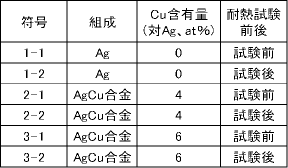
その結果、Cuの含有量を6at%としたときが、耐熱試験後の透過率の低下が最も少なかった。一方、Cuの含有量が多いほど、着色が多い傾向にあった。
前記金属薄膜層の平均厚みとしては、特に制限はなく、目的に応じて適宜選択することができ、例えば、5nm~50nmであってもよいし、10nm~30nmであってもよいし、15nm~25nmであってもよい。
ここで、平均厚みは、透過型電子顕微鏡を用いて、任意の10箇所を測定した際の算術平均値である。
ここで、平均厚みは、透過型電子顕微鏡を用いて、任意の10箇所を測定した際の算術平均値である。
<誘導体層>
前記赤外線反射顔料において、前記誘電体層は、前記金属薄膜層の両面に配される。
前記誘電体層は、例えば、透明であり、前記金属薄膜層の可視光周辺域における反射防止層として機能する。即ち、前記誘電体層は、可視光周辺域の入射光の透過率を向上させる機能を有する。
前記赤外線反射顔料において、前記誘電体層は、前記金属薄膜層の両面に配される。
前記誘電体層は、例えば、透明であり、前記金属薄膜層の可視光周辺域における反射防止層として機能する。即ち、前記誘電体層は、可視光周辺域の入射光の透過率を向上させる機能を有する。
前記誘電体層は、酸化チタンを含有することが好ましく、TiO2、Ti4O7、及びTi3O5の少なくともいずれかを含有することがより好ましく、Ti4O7、及びTi3O5の少なくともいずれかを含有することが更により好ましく、Ti4O7を含有することが特に好ましい。
前記誘電体層は、例えば、蒸着により形成されるが、その際、蒸着源が均一に溶解するためには、蒸着源が導電性を有することが好ましい。蒸着の際に蒸着源が均一に溶解していないと、形成される誘電体層において、点状の膜欠陥が生じる恐れがある。ここで、TiO2は導電性がないが、Ti4O7、Ti3O5、及びTiOは、導電性を有する。
一方、Ti4O7、Ti3O5、及びTiOは、TiO2と比べて透明性が低い恐れがある。
そこで、Ti4O7、Ti3O5、TiO、及びTiO2について、透明性(透過損失)を調べた。
試験片は、蒸着法により、ガラス基板上に、50nm厚みの誘電体層(酸化チタン層)を形成することで作製した。
透過損失は、分光光度計(日本分光社製)を用いて、400nm~700nmの範囲で測定した。結果を図6に示した。
図6より、透過損失が少ない点で、Ti4O7、Ti3O5が好ましく、Ti4O7がより好ましいことが確認できた。
一方、Ti4O7、Ti3O5、及びTiOは、TiO2と比べて透明性が低い恐れがある。
そこで、Ti4O7、Ti3O5、TiO、及びTiO2について、透明性(透過損失)を調べた。
試験片は、蒸着法により、ガラス基板上に、50nm厚みの誘電体層(酸化チタン層)を形成することで作製した。
透過損失は、分光光度計(日本分光社製)を用いて、400nm~700nmの範囲で測定した。結果を図6に示した。
図6より、透過損失が少ない点で、Ti4O7、Ti3O5が好ましく、Ti4O7がより好ましいことが確認できた。
前記誘電体層の各層の平均厚みとしては、特に制限はなく、目的に応じて適宜選択することができ、例えば、10nm~100nmであってもよいし、20nm~50nmであってもよいし、25nm~35nmであってもよい。
ここで、平均厚みは、透過型電子顕微鏡を用いて、任意の10箇所を測定した際の算術平均値である。
ここで、平均厚みは、透過型電子顕微鏡を用いて、任意の10箇所を測定した際の算術平均値である。
ここで、前記赤外線反射顔料の好適構造を以下に示す。
(1)金属薄膜層は、AgCuを含有する。
(2)金属薄膜層の平均厚みは、15nm~25nmである。
(3)誘電体層は、Ti4O7を含有する。
(4)誘電体層の平均厚みは、25nm~35nmである。
(5)誘電体層と、金属薄膜層と、誘電体層とをこの順で積層した構造である。
上記(1)~(5)を満たす赤外線反射顔料の分光特性を図7に示す。
図7の分光特性は、分光光度計(日本分光社製)を用いて、400nm~700nmの範囲で測定した結果である。
測定においては、基板上に赤外線反射顔料と同じ層構造を蒸着法により形成し、粉砕して赤外線反射顔料とする前の状態の試験片を用いた。試験片の層構造は、誘電体層(Ti4O7、30nm)/金属薄膜層(AgCu、20nm)/誘電体層(Ti4O7、30nm)の3層構造である。
また、比較するために、誘電体層(TiO2、35nm)/金属薄膜層(AgPd、10nm)/誘電体層(TiO2、60nm)/金属薄膜層(AgPd、10nm)/誘電体層(TiO2、35nm)の5層構造の赤外線反射顔料の分光特性を、同様の方法で測定した。結果を図8に示した。
図7と図8とを比較すると、上記(1)~(5)を満たす赤外反射顔料では、透過率と反射率とのバランスに優れていた。
また、上記(1)~(5)を満たす赤外反射顔料では、目視による色味もほとんど観察されなかった。これは、金属薄膜層の吸収・反射特性と、誘電体層の吸収・反射特性とを考慮し、金属薄膜層と誘電体層とを積層した際の各吸収・反射特性の重ね合わせにより色味がなくなるように、金属薄膜層の厚み及び誘電体層の厚みを調整したことによる。
(1)金属薄膜層は、AgCuを含有する。
(2)金属薄膜層の平均厚みは、15nm~25nmである。
(3)誘電体層は、Ti4O7を含有する。
(4)誘電体層の平均厚みは、25nm~35nmである。
(5)誘電体層と、金属薄膜層と、誘電体層とをこの順で積層した構造である。
上記(1)~(5)を満たす赤外線反射顔料の分光特性を図7に示す。
図7の分光特性は、分光光度計(日本分光社製)を用いて、400nm~700nmの範囲で測定した結果である。
測定においては、基板上に赤外線反射顔料と同じ層構造を蒸着法により形成し、粉砕して赤外線反射顔料とする前の状態の試験片を用いた。試験片の層構造は、誘電体層(Ti4O7、30nm)/金属薄膜層(AgCu、20nm)/誘電体層(Ti4O7、30nm)の3層構造である。
また、比較するために、誘電体層(TiO2、35nm)/金属薄膜層(AgPd、10nm)/誘電体層(TiO2、60nm)/金属薄膜層(AgPd、10nm)/誘電体層(TiO2、35nm)の5層構造の赤外線反射顔料の分光特性を、同様の方法で測定した。結果を図8に示した。
図7と図8とを比較すると、上記(1)~(5)を満たす赤外反射顔料では、透過率と反射率とのバランスに優れていた。
また、上記(1)~(5)を満たす赤外反射顔料では、目視による色味もほとんど観察されなかった。これは、金属薄膜層の吸収・反射特性と、誘電体層の吸収・反射特性とを考慮し、金属薄膜層と誘電体層とを積層した際の各吸収・反射特性の重ね合わせにより色味がなくなるように、金属薄膜層の厚み及び誘電体層の厚みを調整したことによる。
前記赤外線反射顔料の製造方法としては、特に制限はなく、目的に応じて適宜選択することができ、例えば、支持体上に、金属薄膜層、及び誘電体層を有する積層体を形成した後に、支持体から積層体を剥離し、積層体を粉砕する方法などが挙げられる。
支持体上に、金属薄膜層、誘電体層を形成する方法としては、特に制限はなく、目的に応じて適宜選択することができ、例えば、化学気相蒸着法(CVD)、スパッタリング法、電子ビーム蒸着法(EB)、イオンプレーティング法などが挙げられる。
支持体上に、金属薄膜層、誘電体層を形成する方法としては、特に制限はなく、目的に応じて適宜選択することができ、例えば、化学気相蒸着法(CVD)、スパッタリング法、電子ビーム蒸着法(EB)、イオンプレーティング法などが挙げられる。
ここで、赤外線反射顔料の層構造の一例を図を用いて説明する。
図9は、赤外線反射顔料の層構造の一例を示す断面模式図である。
図9の赤外線反射顔料10は、誘電体層2Aと、金属薄膜層1と、誘電体層2Bとをこの順で有する。
図9は、赤外線反射顔料の層構造の一例を示す断面模式図である。
図9の赤外線反射顔料10は、誘電体層2Aと、金属薄膜層1と、誘電体層2Bとをこの順で有する。
図10は、赤外線反射顔料の層構造の他の一例を示す断面模式図である。
図10の赤外線反射顔料10は、誘電体層2Aと、金属薄膜層1Aと、誘電体層2Bと、金属薄膜層1Bと、誘電体層2Cとをこの順で有する。
図10の赤外線反射顔料10は、誘電体層2Aと、金属薄膜層1Aと、誘電体層2Bと、金属薄膜層1Bと、誘電体層2Cとをこの順で有する。
本発明の赤外線反射顔料は、耐熱性に優れ、かつ反射率が良好であることから、塗料に配合する遮熱顔料として好適に用いることができる。
1 金属薄膜層
1A 金属薄膜層
1B 金属薄膜層
2A 誘電体層
2B 誘電体層
2C 誘電体層
10 赤外線反射顔料
1A 金属薄膜層
1B 金属薄膜層
2A 誘電体層
2B 誘電体層
2C 誘電体層
10 赤外線反射顔料
Claims (10)
- 金属薄膜層と前記金属薄膜層の両面に配された誘電体層とを有し、
前記金属薄膜層が、AgCu合金、及びAgBiNd合金の少なくともいずれかを含有し、
前記誘電体層が、酸化チタンを含有する、
ことを特徴とする赤外線反射顔料。 - 前記金属薄膜層が、AgCu合金を含有する請求項1に記載の赤外線反射顔料。
- 前記AgCu合金におけるCuの含有量が、Agに対して、0at%超30at%以下である請求項2に記載の赤外線反射顔料。
- 前記AgCu合金におけるCuの含有量が、Agに対して、5at%以上20at%以下である請求項2から3のいずれかに記載の赤外線反射顔料。
- 前記酸化チタンが、Ti4O7、及びTi3O5の少なくともいずれかを含有する請求項1から4のいずれかに記載の赤外線反射顔料。
- 前記酸化チタンが、Ti4O7を含有する請求項1から5のいずれかに記載の赤外線反射顔料。
- 前記金属薄膜層の平均厚みが、10nm~30nmである請求項1から6のいずれかに記載の赤外線反射顔料。
- 前記金属薄膜層の平均厚みが、15nm~25nmである請求項1から7のいずれかに記載の赤外線反射顔料。
- 前記誘電体層の平均厚みが、20nm~50nmである請求項1から8のいずれかに記載の赤外線反射顔料。
- 前記誘電体層の平均厚みが、25nm~35nmである請求項1から9のいずれかに記載の赤外線反射顔料。
Applications Claiming Priority (2)
| Application Number | Priority Date | Filing Date | Title |
|---|---|---|---|
| JP2019-045546 | 2019-03-13 | ||
| JP2019045546A JP2020147661A (ja) | 2019-03-13 | 2019-03-13 | 赤外線反射顔料 |
Publications (1)
| Publication Number | Publication Date |
|---|---|
| WO2020184694A1 true WO2020184694A1 (ja) | 2020-09-17 |
Family
ID=72427135
Family Applications (1)
| Application Number | Title | Priority Date | Filing Date |
|---|---|---|---|
| PCT/JP2020/010973 Ceased WO2020184694A1 (ja) | 2019-03-13 | 2020-03-12 | 赤外線反射顔料 |
Country Status (2)
| Country | Link |
|---|---|
| JP (1) | JP2020147661A (ja) |
| WO (1) | WO2020184694A1 (ja) |
Cited By (1)
| Publication number | Priority date | Publication date | Assignee | Title |
|---|---|---|---|---|
| WO2021206062A1 (ja) * | 2020-04-09 | 2021-10-14 | 日本ペイントホールディングス株式会社 | 赤外反射性顔料、塗料組成物、塗膜および物品 |
Families Citing this family (1)
| Publication number | Priority date | Publication date | Assignee | Title |
|---|---|---|---|---|
| JP2022064710A (ja) * | 2020-10-14 | 2022-04-26 | 尾池工業株式会社 | 鱗片状顔料、分散液、塗料、及び塗膜 |
Citations (6)
| Publication number | Priority date | Publication date | Assignee | Title |
|---|---|---|---|---|
| JP2002141694A (ja) * | 2000-10-31 | 2002-05-17 | Furuya Kinzoku:Kk | 電磁波遮蔽膜及びこれを用いた電磁波遮蔽積層体 |
| JP2009051713A (ja) * | 2007-08-29 | 2009-03-12 | Bridgestone Corp | 熱線遮蔽性合わせガラス |
| JP2011520000A (ja) * | 2008-05-09 | 2011-07-14 | ビーエーエスエフ ソシエタス・ヨーロピア | 金属酸化物/水酸化物層およびアクリルコポリマーで塗布された真珠箔顔料 |
| WO2016006664A1 (ja) * | 2014-07-10 | 2016-01-14 | 日本ペイントホールディングス株式会社 | 赤外反射性顔料及び赤外反射性塗料組成物 |
| JP2017030348A (ja) * | 2015-08-04 | 2017-02-09 | 株式会社神戸製鋼所 | 積層膜及び熱線反射材 |
| JP2019085482A (ja) * | 2017-11-06 | 2019-06-06 | トヨタ自動車株式会社 | 赤外線反射顔料の粉末を製造する方法 |
-
2019
- 2019-03-13 JP JP2019045546A patent/JP2020147661A/ja active Pending
-
2020
- 2020-03-12 WO PCT/JP2020/010973 patent/WO2020184694A1/ja not_active Ceased
Patent Citations (6)
| Publication number | Priority date | Publication date | Assignee | Title |
|---|---|---|---|---|
| JP2002141694A (ja) * | 2000-10-31 | 2002-05-17 | Furuya Kinzoku:Kk | 電磁波遮蔽膜及びこれを用いた電磁波遮蔽積層体 |
| JP2009051713A (ja) * | 2007-08-29 | 2009-03-12 | Bridgestone Corp | 熱線遮蔽性合わせガラス |
| JP2011520000A (ja) * | 2008-05-09 | 2011-07-14 | ビーエーエスエフ ソシエタス・ヨーロピア | 金属酸化物/水酸化物層およびアクリルコポリマーで塗布された真珠箔顔料 |
| WO2016006664A1 (ja) * | 2014-07-10 | 2016-01-14 | 日本ペイントホールディングス株式会社 | 赤外反射性顔料及び赤外反射性塗料組成物 |
| JP2017030348A (ja) * | 2015-08-04 | 2017-02-09 | 株式会社神戸製鋼所 | 積層膜及び熱線反射材 |
| JP2019085482A (ja) * | 2017-11-06 | 2019-06-06 | トヨタ自動車株式会社 | 赤外線反射顔料の粉末を製造する方法 |
Cited By (1)
| Publication number | Priority date | Publication date | Assignee | Title |
|---|---|---|---|---|
| WO2021206062A1 (ja) * | 2020-04-09 | 2021-10-14 | 日本ペイントホールディングス株式会社 | 赤外反射性顔料、塗料組成物、塗膜および物品 |
Also Published As
| Publication number | Publication date |
|---|---|
| JP2020147661A (ja) | 2020-09-17 |
Similar Documents
| Publication | Publication Date | Title |
|---|---|---|
| US5521765A (en) | Electrically-conductive, contrast-selectable, contrast-improving filter | |
| JP5864555B2 (ja) | 低いソーラファクターを有する太陽光制御板ガラス | |
| CN105307995B (zh) | 装备有部分金属层的堆叠体的基材、窗玻璃和方法 | |
| TWI480349B (zh) | 塗敷膜及包含該塗敷膜的建築材料 | |
| EP3396454B1 (en) | Reflective transparent screen | |
| KR101768257B1 (ko) | 저방사 코팅 및 이를 포함하는 창호용 건축 자재 | |
| WO2014119683A1 (ja) | 赤外線反射フィルムの製造方法 | |
| JP2005527452A (ja) | 耐摩耗特性を具備した反射防止コーティングを有する透明基材 | |
| TWI583807B (zh) | 透明基板之層系統以及用於生產層系統的方法 | |
| EP3511505A1 (en) | Functional building material for windows and doors | |
| CN109716180B (zh) | 日照遮蔽构件 | |
| CN109564305A (zh) | 具有热性能叠层的基材,其包括至少一层富含锆的硅-锆氮化物,其用途及其制备 | |
| CN112194383A (zh) | 一种低辐射玻璃及其制备方法 | |
| CN110418855B (zh) | 透明光学膜的制造方法及透明多层膜的制造方法 | |
| WO2012115111A1 (ja) | 積層体 | |
| US11531148B2 (en) | Optical coatings for glass and glass laminates | |
| JP6611192B2 (ja) | 低反射コーティング付きガラス板及びそれを用いた合わせガラス | |
| JPH1134216A (ja) | 積層体および窓用ガラス積層体 | |
| CN106536848A (zh) | 低辐射涂层及包括低辐射涂层的窗户用功能性建筑材料 | |
| JP2020147661A (ja) | 赤外線反射顔料 | |
| JP2018519232A (ja) | 熱特性を有し、金属性の終端層を有し、かつ酸化された前終端層を有する積層体、を備えた基材 | |
| JP2007070146A (ja) | 低放射複層ガラス | |
| WO2010098200A1 (ja) | 積層体物品 | |
| JP2020147660A (ja) | 赤外線反射顔料の製造方法、及び積層構造体 | |
| JP2007197237A (ja) | 低放射複層ガラス |
Legal Events
| Date | Code | Title | Description |
|---|---|---|---|
| 121 | Ep: the epo has been informed by wipo that ep was designated in this application |
Ref document number: 20770535 Country of ref document: EP Kind code of ref document: A1 |
|
| NENP | Non-entry into the national phase |
Ref country code: DE |
|
| 122 | Ep: pct application non-entry in european phase |
Ref document number: 20770535 Country of ref document: EP Kind code of ref document: A1 |