WO2020184363A1 - Mixer - Google Patents
Mixer Download PDFInfo
- Publication number
- WO2020184363A1 WO2020184363A1 PCT/JP2020/009345 JP2020009345W WO2020184363A1 WO 2020184363 A1 WO2020184363 A1 WO 2020184363A1 JP 2020009345 W JP2020009345 W JP 2020009345W WO 2020184363 A1 WO2020184363 A1 WO 2020184363A1
- Authority
- WO
- WIPO (PCT)
- Prior art keywords
- signal
- terminal
- input
- wave
- mixer
- Prior art date
Links
Images


Classifications
-
- H—ELECTRICITY
- H03—ELECTRONIC CIRCUITRY
- H03D—DEMODULATION OR TRANSFERENCE OF MODULATION FROM ONE CARRIER TO ANOTHER
- H03D7/00—Transference of modulation from one carrier to another, e.g. frequency-changing
- H03D7/16—Multiple-frequency-changing
- H03D7/165—Multiple-frequency-changing at least two frequency changers being located in different paths, e.g. in two paths with carriers in quadrature
-
- H—ELECTRICITY
- H03—ELECTRONIC CIRCUITRY
- H03D—DEMODULATION OR TRANSFERENCE OF MODULATION FROM ONE CARRIER TO ANOTHER
- H03D7/00—Transference of modulation from one carrier to another, e.g. frequency-changing
- H03D7/14—Balanced arrangements
-
- H—ELECTRICITY
- H03—ELECTRONIC CIRCUITRY
- H03D—DEMODULATION OR TRANSFERENCE OF MODULATION FROM ONE CARRIER TO ANOTHER
- H03D7/00—Transference of modulation from one carrier to another, e.g. frequency-changing
- H03D7/14—Balanced arrangements
- H03D7/1425—Balanced arrangements with transistors
- H03D7/1433—Balanced arrangements with transistors using bipolar transistors
-
- H—ELECTRICITY
- H03—ELECTRONIC CIRCUITRY
- H03D—DEMODULATION OR TRANSFERENCE OF MODULATION FROM ONE CARRIER TO ANOTHER
- H03D7/00—Transference of modulation from one carrier to another, e.g. frequency-changing
- H03D7/14—Balanced arrangements
- H03D7/1425—Balanced arrangements with transistors
- H03D7/1441—Balanced arrangements with transistors using field-effect transistors
-
- H—ELECTRICITY
- H03—ELECTRONIC CIRCUITRY
- H03D—DEMODULATION OR TRANSFERENCE OF MODULATION FROM ONE CARRIER TO ANOTHER
- H03D7/00—Transference of modulation from one carrier to another, e.g. frequency-changing
- H03D7/14—Balanced arrangements
- H03D7/1425—Balanced arrangements with transistors
- H03D7/1458—Double balanced arrangements, i.e. where both input signals are differential
-
- H—ELECTRICITY
- H04—ELECTRIC COMMUNICATION TECHNIQUE
- H04B—TRANSMISSION
- H04B1/00—Details of transmission systems, not covered by a single one of groups H04B3/00 - H04B13/00; Details of transmission systems not characterised by the medium used for transmission
- H04B1/06—Receivers
- H04B1/16—Circuits
- H04B1/30—Circuits for homodyne or synchrodyne receivers
-
- H—ELECTRICITY
- H03—ELECTRONIC CIRCUITRY
- H03D—DEMODULATION OR TRANSFERENCE OF MODULATION FROM ONE CARRIER TO ANOTHER
- H03D2200/00—Indexing scheme relating to details of demodulation or transference of modulation from one carrier to another covered by H03D
- H03D2200/0001—Circuit elements of demodulators
- H03D2200/0019—Gilbert multipliers
-
- H—ELECTRICITY
- H03—ELECTRONIC CIRCUITRY
- H03D—DEMODULATION OR TRANSFERENCE OF MODULATION FROM ONE CARRIER TO ANOTHER
- H03D2200/00—Indexing scheme relating to details of demodulation or transference of modulation from one carrier to another covered by H03D
- H03D2200/0041—Functional aspects of demodulators
- H03D2200/0088—Reduction of intermodulation, nonlinearities, adjacent channel interference; intercept points of harmonics or intermodulation products
-
- H—ELECTRICITY
- H03—ELECTRONIC CIRCUITRY
- H03D—DEMODULATION OR TRANSFERENCE OF MODULATION FROM ONE CARRIER TO ANOTHER
- H03D2200/00—Indexing scheme relating to details of demodulation or transference of modulation from one carrier to another covered by H03D
- H03D2200/0041—Functional aspects of demodulators
- H03D2200/009—Reduction of local oscillator or RF leakage
Definitions
- the present invention relates to a mixer having a plurality of unit mixers.
- the mixer used in the transmitter is composed of a circuit that up-converts a baseband signal to a desired frequency band in a direct conversion system or a heterodyne system communication system.
- Such mixers have a first unit mixer, a second unit mixer, and a first synthesizer.
- the first unit mixer takes a locally oscillated wave as an input and up-converts an I-channel baseband signal.
- the local oscillator wave will be referred to as an LO (Local Oscillation) wave.
- the second unit mixer takes an LO wave having a phase difference of 90 ° with respect to the LO wave of the first unit mixer as an input, and up-converts the baseband signal of the Q channel.
- the first synthesizer synthesizes the output signal of the first unit mixer and the output signal of the second unit mixer.
- Mixers are generally required to suppress unnecessary spurious emissions that appear in output signals in order to achieve good communication.
- the communication semiconductor integrated circuit has a frequency dividing circuit for generating an input signal to be supplied to a mixer that up-converts a transmission signal.
- the frequency dividing circuit generates the input signal by dividing the local oscillation signal.
- the frequency dividing circuit is configured by using a Gilbert cell type circuit having a lower differential transistor and an upper differential transistor.
- a MOS (Metal-Oxide-Semiconductor) transistor is used as the lower differential transistor, and a bipolar transistor is used as the upper differential transistor.
- a large number of unnecessary spurs are generated in the output of the mixer.
- an LPF Low Pass Filter
- the transmission system semiconductor integrated circuit apparatus described in Patent Document 2 includes a phase partitioning means that phase-distributes the first local signal to 0/90 ° and amplitude equalization that eliminates the amplitude error component of the phase-distributed local signal.
- a means a quadrature modulation mixer that outputs a quadrature modulated wave by multiplying a phase-distributed local signal and a baseband signal, and a frequency mixer that multiplies the quadrature modulated wave and a second local signal are provided. There is. At this time, a large number of unnecessary spurs are generated in the output of the quadrature modulation mixer. In order to suppress this unnecessary spurious, the first LPF is installed in the input front stage of the quadrature modulation mixer, and the second LPF is installed in the output rear stage of the quadrature modulation mixer.
- An amplifier that amplifies a baseband signal is generally used in front of a transmission mixer as described in Patent Document 1 or Patent Document 2.
- CMRR Common Mode Rejection Ratio
- a common-mode signal is included in the dynamic signal. In that case, there is a problem that the in-phase signal becomes unnecessary spurious and occurs at the output terminal due to the asymmetry of the load after up-converting the differential signal with the orthogonal mixer.
- the present invention has been made to solve such a problem, and an object of the present invention is to provide a mixer capable of suppressing unnecessary spurious caused by an in-phase signal in a mixer for transmission.
- the present invention outputs a signal obtained by multiplying a baseband signal terminal, an LO input terminal, a signal input to the baseband signal terminal, and a locally oscillating wave input to the LO input terminal.
- a unit mixer from the first to the fourth having the same configuration which includes a signal terminal and at least one of the base band signal terminal and the RF signal terminal is a differential terminal, and a first input.
- a first signal is input, the first input signal is distributed in phase, and a signal having the same phase is given to the baseband signal terminal of the first unit mixer and the baseband signal terminal of the second unit mixer.
- the input terminal and the second input signal are input, and the second input signal is distributed in phase to the baseband signal terminal of the third unit mixer and the baseband signal of the fourth unit mixer.
- the first unit mixer includes a second input terminal that gives in-phase signals to the terminals and a synthesizer that synthesizes signals output from the RF signal terminals of the first to fourth unit mixers.
- a first local oscillation wave and a second local oscillation wave, which are orthogonal to each other, are input to the LO input terminal and the LO input terminal of the second unit mixer, respectively, and the third unit mixer
- a third local oscillation wave and a fourth local oscillation wave, which are orthogonal to each other, are input to the LO input terminal and the LO input terminal of the fourth unit mixer, respectively, and the first local oscillation wave is the said.
- the phase of the second local oscillation wave is different from that of either the third local oscillation wave or the fourth local oscillation wave by 180 °, and the second local oscillation wave is the third local oscillation wave or the fourth local oscillation wave.
- One of the differential terminals has a 180 ° phase difference from that of any one, and one of the differential terminals is a mixer having an inverted connection relationship with the other differential terminal.
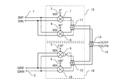
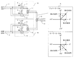
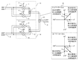
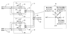
- FIG. It is a figure which shows one configuration example of the transmission mixer which concerns on Embodiment 1.
- FIG. It is a figure which shows the phase relation of the differential signal in the I channel which concerns on Embodiment 1.
- FIG. It is a figure which shows the phase relation of the differential signal in the Q channel which concerns on Embodiment 1.
- FIG. It is a figure which shows the phase relation of the differential signal after synthesis which concerns on Embodiment 1.
- FIG. It is a figure which shows the phase relation of the common mode signal in the I channel which concerns on Embodiment 1.
- FIG. It is a figure which shows the phase relation of the common mode signal in the Q channel which concerns on Embodiment 1.
- FIG. It is a figure which shows the phase relation of the common mode signal after synthesis which concerns on Embodiment 1.
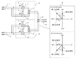
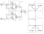
- FIG. It is a figure which shows one configuration example of the transmission mixer which concerns on Embodiment 2.
- FIG. It is a figure which shows the phase relation of the differential signal in the I channel which concerns on Embodiment 2.
- FIG. It is a figure which shows the phase relation of the differential signal in the Q channel which concerns on Embodiment 2.
- FIG. It is a figure which shows the phase relation of the common mode signal in the Q channel which concerns on Embodiment 2.
- FIG. 1 shows the phase relation of LO leak in the I channel which concerns on Embodiment 2.
- FIG. 2 is a figure which shows the phase relation of LO leak in the Q channel which concerns on Embodiment 2.
- FIG. 1 shows the phase relation of LO leak after synthesis which concerns on Embodiment 2.
- FIG. 1 shows the 1st unit mixer which concerns on Embodiment 3.
- FIG. 1 shows the 1st unit mixer which concerns on Embodiment 3.
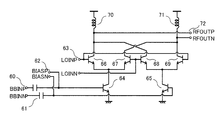
- FIG. 1 is a diagram showing a configuration example of a mixer according to a first embodiment of the present invention.
- a mixer used as a transmission mixer will be described as an example, but the present embodiment is not limited to this.
- the mixer according to the first embodiment is the output of the first input terminal 1, the second input terminal 2, the first orthogonal mixer 15, the second orthogonal mixer 16, and the first orthogonal mixer 15. It includes a first synthesizer 13 that synthesizes a signal and an output signal of the second orthogonal mixer 16, and a first output terminal 14.
- the first orthogonal mixer 15 includes a first unit mixer 7, a second unit mixer 8, and a second synthesizer 11.
- the first unit mixer 7 has a baseband signal terminal and an RF (Radio Frequency) signal terminal, and also has a first LO input terminal 3 to which a 0 ° LO wave as a first LO wave is input. ..
- the baseband signal terminal and the RF signal terminal of the first unit mixer 7 are both composed of differential terminals.
- the second unit mixer 8 has a baseband signal terminal and an RF signal terminal, and also has a second LO input terminal 4 to which a 90 ° LO wave as a second LO wave is input.
- the baseband signal terminal and the RF signal terminal of the second unit mixer 8 are both composed of differential terminals.
- the second synthesizer 11 synthesizes the output signal of the first unit mixer 7 and the output signal of the second unit mixer 8. Both the first LO wave and the second LO wave are input from a first LO wave oscillator (not shown).
- the first LO wave oscillator is composed of, for example, an orthogonal oscillator.
- both the baseband signal terminal and the RF signal terminal are configured as differential terminals.
- One of them may be configured as a differential terminal.
- the differential terminal is a terminal in which two terminals are provided in parallel, the original signal is input to one terminal, and the signal in which the polarity of the original signal is inverted is input to the other terminal. That is.
- the first unit mixer 7 and the second unit mixer 8 have the same configuration. As LO waves given to the first unit mixer 7 and the second unit mixer 8, the cases where the phases are 0 ° and 90 °, respectively, have been described, but not limited to that case, they are orthogonal to each other. If it is a certain LO wave, the phase is not particularly limited.
- the second orthogonal mixer 16 includes a third unit mixer 9, a fourth unit mixer 10, and a third synthesizer 12.
- the third unit mixer 9 has a baseband signal terminal and an RF signal terminal, and also has a third LO input terminal 5 to which a 270 ° LO wave as a third LO wave is input.
- the baseband signal terminal and the RF signal terminal of the third unit mixer 9 are both composed of differential terminals. Further, as shown in FIG. 1, the RF signal terminal of the third unit mixer 9 is connected to the third synthesizer 12 with its polarity reversed.
- the fourth unit mixer 10 has a baseband signal terminal and an RF signal terminal, and also has a fourth LO input terminal 6 into which a 180 ° LO wave as a fourth LO wave is input.
- the baseband signal terminal and the RF signal terminal of the fourth unit mixer 10 are both composed of differential terminals.
- the third synthesizer 12 synthesizes the output signal of the third unit mixer 9 and the output signal of the fourth unit mixer 10.
- Both the third LO wave and the fourth LO wave are input from a second LO wave oscillator (not shown).
- the second LO wave oscillator is composed of, for example, an orthogonal oscillator.
- both the baseband signal terminal and the RF signal terminal are configured as differential terminals.
- One of them may be configured as a differential terminal.
- the third unit mixer 9 and the fourth unit mixer 10 have the same configuration.
- the cases where the phases are 270 ° and 180 °, respectively, have been described, but not limited to this case, they are orthogonal to each other. If it is a certain LO wave, the phase is not particularly limited.
- the LO wave oscillated from the first LO wave oscillator and the LO wave oscillated from the second LO wave oscillator are 180 ° out of phase.
- the LO wave input to the first unit mixer 7 and the LO wave input to the fourth unit mixer 10 are described as having 180 ° out-of-phase, but the first unit mixer 7 has been described.
- the LO wave input and the LO wave input to the third unit mixer 9 may be configured to be 180 ° out of phase.
- the LO wave input to the second unit mixer 8 and the LO wave input to the third unit mixer 9 have been described as having 180 ° out-of-phase, but they are input to the second unit mixer 8.
- the LO wave to be generated and the LO wave input to the fourth unit mixer 10 may have a 180 ° phase difference.
- the first input signal input to the first input terminal 1 is distributed in phase to the second signal and the third signal, and is input to the first orthogonal mixer 15.
- the second signal is input to the baseband signal terminal of the first unit mixer 7, and the third signal is input to the baseband signal terminal of the second unit mixer 8.
- the first unit mixer 7 multiplies the second signal by the 0 ° LO wave input from the first LO input terminal 3, and outputs the fourth signal from the RF signal terminal.
- the second unit mixer 8 multiplies the third signal by the 90 ° LO wave input from the second LO input terminal 4, and outputs the fifth signal from the RF signal terminal.
- the second synthesizer 11 synthesizes the fourth signal and the fifth signal, and outputs the sixth signal.
- the second input signal input to the second input terminal 2 is distributed in phase to the seventh signal and the eighth signal, and is input to the second orthogonal mixer 16.
- the seventh signal is input to the baseband signal terminal of the third unit mixer 9, and the eighth signal is input to the baseband signal terminal of the fourth unit mixer 10.
- the third unit mixer 9 multiplies the seventh signal by the 270 ° LO wave input from the third LO input terminal 5, inverts the RF signal terminal, and outputs the ninth signal.
- the fourth unit mixer 10 multiplies the eighth signal by the 180 ° LO wave input from the fourth LO input terminal 6, and outputs the tenth signal from the RF signal terminal.
- the third synthesizer 12 synthesizes the ninth signal and the tenth signal, and outputs the eleventh signal.
- the first synthesizer 13 synthesizes the sixth signal and the eleventh signal, and outputs the sixth signal to the outside from the first output terminal 14.
- the orthogonal mixers 15 and 16 are composed of four unit mixers 7 to 10 having the same configuration. Further, there are four phases having a phase difference of 90 ° with respect to these four unit mixers, that is, the first unit mixer 7, the second unit mixer 8, the third unit mixer 9, and the fourth unit mixer 10.
- LO waves that is, LO waves of 0 °, 90 °, 180 °, and 270 ° are used, respectively.
- the output signals of the first orthogonal mixer 15 and the second orthogonal mixer 16 are synthesized. ..
- the output of the third unit mixer 9 for inputting the LO wave of 270 ° has its polarity reversed and is connected to the third synthesizer 12 in the subsequent stage.
- the configurations of the fourth unit mixer 10, the second synthesizer 11, and the third synthesizer 12 are merely examples, and are not limited thereto, and other configurations may be used. Needless to say, it's good. Further, in FIG. 1, three synthesizers 11 to 13 are provided, but one synthesizer may synthesize the outputs of the four unit mixers 7 to 10.
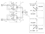
- FIG. 2 is a diagram showing a phase relationship of differential signals in the I channel according to the first embodiment.
- the amplitude of the amplitude and the fifth signal of the fourth signal are both V I, when the amplitude of the sixth signal and V I ', the phase and amplitude of the sixth signal, shown by reference numeral A in FIG. 2
- the vector diagram shows the upper local case and the lower local case, respectively.
- the upper local is a word indicating a state in which the frequency of each of the first to fourth LO waves is set higher than the frequency of the RF signal.
- the lower local is a word indicating a state in which the frequency of each of the first to fourth LO waves is set lower than the frequency of the RF signal.
- the phases and amplitudes of the fourth signal, the fifth signal, and the sixth signal are as follows.
- FIG. 3 is a diagram showing a phase relationship of differential signals in the Q channel according to the first embodiment. Assuming that the amplitude of the ninth signal and the amplitude of the tenth signal are both V Q and the amplitude of the eleventh signal is V Q ', the phase and amplitude of the eleventh signal are shown by reference numeral B in FIG. It is represented by a vector diagram. The vector diagram shows the upper local case and the lower local case, respectively. The phases and amplitudes of the ninth signal, the tenth signal, and the eleventh signal are as follows.
- FIG. 4 is a diagram showing the phase relationship of the differential signal after synthesis according to the first embodiment.
- the phase and amplitude of the sixth signal and the eleventh signal at the first output terminal 14 are represented by the vector diagram indicated by reference numeral C in FIG.
- the vector diagram shows the upper local case and the lower local case, respectively.
- each phase and each amplitude of the sixth signal and the eleventh signal are as follows.
- FIG. 5 is a diagram showing a phase relationship of in-phase signals in the I channel according to the first embodiment.
- the amplitude of the phase signal between the differential occurring respectively in the fourth signal and the fifth signal and both V cm, when the amplitude of the phase signal between the differential occurring in the sixth signal and V cm ', the The phase and amplitude of the differential in-phase signals generated in signal 6 are represented by the vector diagram shown by reference numeral D in FIG.
- the vector diagram shows the upper local case and the lower local case, respectively.
- the phases and amplitudes of the differential in-phase signal generated in the fourth signal, the differential-phase in-phase signal generated in the fifth signal, and the differential-phase in-phase signal generated in the sixth signal are , Is as follows.
- FIG. 6 is a diagram showing a phase relationship of in-phase signals in the Q channel according to the first embodiment.
- the amplitudes of the differential in-phase signals generated in the ninth signal and the tenth signal are both V cm and the amplitudes of the differential-phase signals generated in the eleventh signal are V cm '.
- the phase and amplitude of the differential in-phase signals generated in the 11 signals are represented by the vector diagram shown by reference numeral E in FIG.
- the vector diagram shows the upper local case and the lower local case, respectively.
- the phases and amplitudes of the differential in-phase signal generated in the ninth signal, the differential-phase in-phase signal generated in the tenth signal, and the differential-phase in-phase signal generated in the eleventh signal are , Is as follows.
- FIG. 7 is a diagram showing a phase relationship of in-phase signals after synthesis according to the first embodiment.
- the phase and amplitude of the sixth signal and the eleventh signal at the first output terminal 14 are represented by the vector diagram indicated by reference numeral F in FIG.
- the vector diagram shows the upper local case and the lower local case, respectively.
- each phase and each amplitude of the sixth signal and the eleventh signal are as follows.
- the in-phase signal of the I channel and the in-phase signal of the Q channel are combined with the same amplitude and opposite phase, so that the in-phase signal is canceled.
- the orthogonal mixers 15 and 16 are composed of four unit mixers 7 to 10 having the same configuration. Further, by using the first LO wave oscillator and the second LO wave oscillator having 180 ° phases different from each other, the four unit mixers, that is, the first unit mixer 7, the second unit mixer 8, and the third unit mixer A four-phase LO wave having a phase difference of 90 ° is input to each of the unit mixer 9 and the fourth unit mixer 10. Further, by providing the first synthesizer 13, the second synthesizer 11, and the third synthesizer 12, the output signals of the first orthogonal mixer 15 and the second orthogonal mixer 16 are synthesized. As shown in 7, the in-phase signal component is canceled.
- the first orthogonal mixer 15 operates with the output of the first orthogonal mixer 15 operating in the LO wave of 0 ° and 90 °, and the LO wave of 180 ° and 270 ° which is the LO wave having the opposite phase to the first orthogonal mixer 15.
- the output signal is canceled by synthesizing the output of the second orthogonal mixer 16.
- simply using the LO wave of the opposite phase cancels both the differential signal and the in-phase signal. Therefore, in the first embodiment, only one differential terminal is inverted and the third differential terminal is inverted. It is connected to the synthesizer 12. By doing so, the polarity of the differential signal is inverted before and after the portion where the differential terminal is inverted, and the polarity of the in-phase signal remains the same.
- the differential signal a signal equivalent to that of a normal mixer can be obtained, and only the in-phase signal can be canceled.
- this configuration can suppress unnecessary spurious generated by mixing in-phase components such as power supply noise into the differential input.
- the RF signal terminal is composed of the differential terminal of any of the first, second, third, and fourth unit mixers 7 to 10. The same operation can be realized even when the above is inverted and connected. Further, the baseband signal terminal may be single-phase as long as the first, second, third, and fourth unit mixers 7 to 10 have the same configuration. Further, in the first embodiment, if a 90 ° phase difference distribution unit is provided in front of the first input terminal 1 and the second input terminal 2, the mixer according to the first embodiment can be imaged. It is also possible to operate as a rejection mixer.
- the 90 ° phase difference distribution unit inputs the third input signal.
- the 90 ° phase difference distribution unit generates, from the third input signal, a first input signal input to the first input terminal 1 and a second signal input to the second input terminal 2.
- the 90 ° phase difference distributor may be composed of, for example, a 90 ° phase difference distributor and a 90 ° phase shifter, or may be composed of an in-phase distributor and a 90 ° phase shifter.
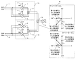
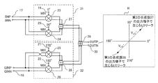
- FIG. 8 is a diagram showing a configuration example of a mixer according to a second embodiment of the present invention.
- a mixer used as a transmission mixer will be described as an example, but the present invention is not limited to this.
- the mixer according to the second embodiment is the output of the first input terminal 17, the second input terminal 18, the first orthogonal mixer 31, the second orthogonal mixer 32, and the first orthogonal mixer 31. It includes a first synthesizer 29 that synthesizes a signal and an output signal of the second orthogonal mixer 32, and a first output terminal 30.
- the first orthogonal mixer 31 includes a first unit mixer 23, a second unit mixer 24, and a second synthesizer 27.
- the first unit mixer 23 has a baseband signal terminal and an RF signal terminal, and also has a first LO input terminal 19 into which a 0 ° LO wave as a first LO wave is input.
- the baseband signal terminal and the RF signal terminal of the first unit mixer 23 are both composed of differential terminals.
- the second unit mixer 24 has a baseband signal terminal and an RF signal terminal, and also has a second LO input terminal 20 into which a 90 ° LO wave as a second LO wave is input.
- the baseband signal terminal and the RF signal terminal of the second unit mixer 24 are both composed of differential terminals.
- the second synthesizer 27 synthesizes the output signal of the first unit mixer 23 and the output signal of the second unit mixer 24. Both the first LO wave and the second LO wave are input from a first LO wave oscillator (not shown).
- the first LO wave oscillator is composed of, for example, an orthogonal oscillator.
- both the baseband signal terminal and the RF signal terminal are configured as differential terminals.
- One of them may be configured as a differential terminal.
- the first unit mixer 23 and the second unit mixer 24 have the same configuration.
- LO waves given to the first unit mixer 23 and the second unit mixer 24 the cases where the phases are 0 ° and 90 °, respectively, have been described, but not limited to this case, they are orthogonal to each other. If it is a certain LO wave, the phase is not particularly limited.
- the second orthogonal mixer 32 includes a third unit mixer 25, a fourth unit mixer 26, and a third synthesizer 28.
- the third unit mixer 25 has a baseband signal terminal and an RF signal terminal, and also has a third LO input terminal 21 into which a 270 ° LO wave as a third LO wave is input.
- the baseband signal terminal and the RF signal terminal of the third unit mixer 25 are both composed of differential terminals. Further, the baseband signal terminal of the third unit mixer 25 is inverted and connected to the second input terminal 18.
- the fourth unit mixer 26 has a baseband signal terminal and an RF signal terminal, and also has a fourth LO input terminal 22 into which a 180 ° LO wave as a fourth LO wave is input.
- the baseband signal terminal and the RF signal terminal of the fourth unit mixer 26 are both composed of differential terminals.
- the third synthesizer 28 synthesizes the output signal of the third unit mixer 25 and the output signal of the fourth unit mixer 26.
- Both the third LO wave and the fourth LO wave are input from a second LO wave oscillator (not shown).
- the second LO wave oscillator is composed of, for example, an orthogonal oscillator.
- both the baseband signal terminal and the RF signal terminal are configured as differential terminals.
- One of them may be configured as a differential terminal.
- the third unit mixer 25 and the fourth unit mixer 26 have the same configuration.
- the units mixers 23 to 26 from the first to the fourth have the same configuration will be described.
- LO waves given to the third unit mixer 25 and the fourth unit mixer 26 the cases where the phases are 270 ° and 180 °, respectively, have been described, but not limited to this case, they are orthogonal to each other. If it is a certain LO wave, the phase is not particularly limited.
- the LO wave oscillated from the first LO wave oscillator and the LO wave oscillated from the second LO wave oscillator are 180 ° out of phase.
- the LO wave input to the first unit mixer 23 and the LO wave input to the fourth unit mixer 26 are described as having 180 ° out-of-phase, but the first unit mixer 23
- the LO wave input and the LO wave input to the third unit mixer 25 may have a 180 ° phase difference.
- the LO wave input to the second unit mixer 24 and the LO wave input to the third unit mixer 25 are 180 ° out of phase, they are input to the second unit mixer 24.
- the LO wave to be generated and the LO wave input to the fourth unit mixer 26 may have a 180 ° phase difference.
- the first input signal input to the first input terminal 17 is distributed in phase to the second signal and the third signal, and is input to the first orthogonal mixer 31.
- the second signal is input to the baseband signal terminal of the first unit mixer 23, and the third signal is input to the baseband signal terminal of the second unit mixer 24.
- the first unit mixer 23 multiplies the second signal by the 0 ° LO wave input from the first LO input terminal 19, and outputs the fourth signal from the RF signal terminal.
- the second unit mixer 24 multiplies the third signal by the 90 ° LO wave input from the second LO input terminal 20, and outputs the fifth signal from the RF signal terminal.
- the second synthesizer 27 synthesizes the fourth signal and the fifth signal, and outputs the sixth signal.
- the second input signal input to the second input terminal 18 is distributed in phase to the seventh signal and the eighth signal, and is input to the second orthogonal mixer 32.
- the seventh signal is input to the baseband signal terminal of the third unit mixer 25, and the eighth signal is input to the baseband signal terminal of the fourth unit mixer 26.
- the third unit mixer 25 multiplies the seventh signal by the 270 ° LO wave input from the third LO input terminal 21, and outputs the ninth signal from the RF signal terminal.
- the baseband signal terminal of the third unit mixer 25 is inverted and connected to the second input terminal 18. Therefore, the polarity of the seventh signal is inverted and input to the baseband signal terminal of the third unit mixer 25.
- the fourth unit mixer 26 multiplies the eighth signal by the 180 ° LO wave input from the fourth LO input terminal 22, and outputs the tenth signal from the RF signal terminal.
- the third synthesizer 28 synthesizes the ninth signal and the tenth signal, and outputs the eleventh signal.
- the first synthesizer 29 synthesizes the sixth signal and the eleventh signal, and outputs the sixth signal to the outside from the first output terminal 30.
- the orthogonal mixers 31 and 32 are composed of four unit mixers 23 to 26 having the same configuration. Further, there is a phase difference of 90 ° with respect to each of the four unit mixers, that is, the first unit mixer 23, the second unit mixer 24, the third unit mixer 25, and the fourth unit mixer 26.
- Four-phase LO waves that is, 0 °, 90 °, 180 °, 270 ° LO waves are used. Further, by providing the first synthesizer 29, the second synthesizer 27, and the third synthesizer 28, the output signals of the first orthogonal mixer 31 and the second orthogonal mixer 32 are synthesized. ..
- the input of the third unit mixer 25 for inputting the LO wave of 270 ° is connected to the second input terminal 18 in the previous stage by reversing the polarity.
- the difference between the second embodiment and the first embodiment is that in the first embodiment, the RF signal terminal of the third unit mixer 9 is configured by a differential terminal, and the differential terminal is inverted. Therefore, it was connected to the third synthesizer 12 in the subsequent stage, but in the second embodiment, the baseband signal terminal of the third unit mixer 25 is configured by the differential terminal, and the differential terminal is inverted. The difference is that it is connected to the second input terminal 18 in the previous stage.
- the configurations of the fourth unit mixer 26, the second synthesizer 27, and the third synthesizer 28 are merely examples, and are not limited thereto, and other configurations may be used. Needless to say, it's good. Further, in FIG. 8, three synthesizers 27 to 29 are provided, but one synthesizer may synthesize the outputs of the four unit mixers 23 to 26.
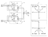
- FIG. 9 is a diagram showing a phase relationship of differential signals in the I channel according to the second embodiment.
- the amplitude of the amplitude and the fifth signal of the fourth signal are both V I, when the amplitude of the sixth signal and V I ', the phase and amplitude of the sixth signal, shown by reference numeral G in FIG. 9 It is represented by a vector diagram.
- the vector diagram shows the upper local case and the lower local case, respectively.
- the phases and amplitudes of the fourth signal, the fifth signal, and the sixth signal are as follows.
- FIG. 10 is a diagram showing a phase relationship of differential signals in the Q channel according to the second embodiment.
- the amplitude of the ninth signal and the amplitude of the tenth signal are both V Q and the amplitude of the eleventh signal is V Q '
- the phase and amplitude of the eleventh signal are shown in FIG. It is represented by the vector diagram shown by the reference numeral H in 10.
- the vector diagram shows the upper local case and the lower local case, respectively.
- the phases and amplitudes of the ninth signal, the tenth signal, and the eleventh signal are as follows.
- FIG. 11 is a diagram showing the phase relationship of the differential signal after synthesis according to the second embodiment.
- the phases and amplitudes of the sixth signal and the eleventh signal at the first output terminal 30 are represented by the vector diagram indicated by reference numeral J in FIG.
- the vector diagram shows the upper local case and the lower local case, respectively.
- each phase and each amplitude of the sixth signal and the eleventh signal are as follows.
- the mixer according to the second embodiment operates as an orthogonal mixer because the signal of the I channel and the signal of the Q channel are orthogonal to each other.
- FIG. 12 is a diagram showing a phase relationship of in-phase signals in the I channel according to the second embodiment.
- the amplitude of the phase signal between the differential occurring respectively in the fourth signal and the fifth signal and both V cm, when the amplitude of the phase signal between the differential occurring in the sixth signal and V cm ', the The phase and amplitude of the differential in-phase signals generated in signal 6 are represented by the vector diagram shown by reference numeral K in FIG.
- the vector diagram shows the upper local case and the lower local case, respectively.
- the phases and amplitudes of the differential in-phase signal generated in the fourth signal, the differential-phase in-phase signal generated in the fifth signal, and the differential-phase in-phase signal generated in the sixth signal are , Is as follows.
- FIG. 13 is a diagram showing a phase relationship of in-phase signals in the Q channel according to the second embodiment.
- the amplitudes of the differential in-phase signals generated in the ninth signal and the tenth signal are both V cm and the amplitudes of the differential-phase signals generated in the eleventh signal are V cm '.
- the phase and amplitude of the differential in-phase signals generated in the 11 signals are represented by the vector diagram indicated by reference numeral L in FIG.
- the vector diagram shows the upper local case and the lower local case, respectively.
- the phases and amplitudes of the differential in-phase signal generated in the ninth signal, the differential-phase in-phase signal generated in the tenth signal, and the differential-phase in-phase signal generated in the eleventh signal are , Is as follows.
- FIG. 14 is a diagram showing a phase relationship of in-phase signals after synthesis according to the second embodiment.
- the phase and amplitude of the sixth signal and the eleventh signal at the first output terminal 30 are represented by the vector diagram shown by reference numeral M in FIG.
- the vector diagram shows the upper local case and the lower local case, respectively.
- the phases and amplitudes of the sixth signal and the eleventh signal are as follows.
- FIG. 15 is a diagram showing a phase relationship of LO leaks in the I channel according to the second embodiment.
- the second unit The phase and amplitude of the LO leak generated at the output terminal of the synthesizer 27 are represented by the vector diagram indicated by reference numeral N in FIG.
- the vector diagram shows the upper local case and the lower local case, respectively.
- the phases and amplitudes of the LO leak generated in the first unit mixer 23, the LO leak generated in the second unit mixer 24, and the LO leak generated in the output terminal of the second synthesizer 27 are as follows. ..
- FIG. 16 is a diagram showing a phase relationship of LO leaks in the Q channel according to the second embodiment.
- the third unit is the third.
- the phase and amplitude of the LO leak that occurs at the output terminal of the synthesizer 28 is represented by the vector diagram indicated by reference numeral P in FIG.
- the vector diagram shows the upper local case and the lower local case, respectively.
- the phases and amplitudes of the LO leak generated in the third unit mixer 25, the LO leak generated in the fourth unit mixer 26, and the LO leak generated in the output terminal of the third synthesizer 28 are as follows. ..
- FIG. 17 is a diagram showing a phase relationship of LO leaks after synthesis according to the second embodiment.
- the phase and amplitude of the LO leak occurring at the output terminal of the second synthesizer 27 at the first output terminal 30 and the LO leak occurring at the output terminal of the third synthesizer 28 are shown by reference numeral R in FIG. Represented by a vector diagram.
- the vector diagram shows the upper local case and the lower local case, respectively.
- the phases and amplitudes of the LO leak generated at the output terminal of the second synthesizer 27 and the LO leak generated at the output terminal of the third synthesizer 28 are as follows.
- the first orthogonal mixer 31 and the second orthogonal mixer 32 are composed of four unit mixers 23 to 26 having the same configuration. Further, by using the first LO wave oscillator and the second LO wave oscillator having 180 ° phases different from each other, the four unit mixers, that is, the first unit mixer 23, the second unit mixer 24, and the third unit mixer For each of the unit mixer 25 and the fourth unit mixer 26, a four-phase LO wave having a phase difference of 90 ° is used. Further, by providing the first synthesizer 29, the second synthesizer 27, and the third synthesizer 28, the output signals of the first orthogonal mixer 31 and the second orthogonal mixer 32 are synthesized. The in-phase signal component is canceled.
- the second embodiment only one differential terminal is inverted and the second differential terminal is inverted. It is connected to the input terminal 18. By doing so, the polarity of the differential signal is inverted before and after the portion where the differential terminal is inverted, and the polarity of the in-phase signal remains the same.
- the differential signal a signal equivalent to that of a normal mixer can be obtained, and only the in-phase signal can be canceled.
- this configuration can suppress unnecessary spurious generated by mixing in-phase components such as power supply noise into the differential input.
- the RF signal terminal may be single-phase as long as the first, second, third, and fourth unit mixers have the same configuration.
- the mixer according to the second embodiment can be imaged. It is also possible to operate as a rejection mixer.
- the 90 ° phase difference distributor may be composed of, for example, a 90 ° phase difference distributor and a 90 ° phase shifter, or may be composed of an in-phase distributor and a 90 ° phase shifter.
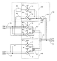
- FIG. 18 is a diagram showing a configuration example of the mixer according to the third embodiment.
- the mixer according to the third embodiment includes a first input terminal 33, a second input terminal 34, a first synthesizer 45, a first output terminal 46, a first orthogonal mixer 47, and a first.
- the orthogonal mixer 48 of 2 and the feedback circuit 59 are provided.
- the first orthogonal mixer 47 includes a first unit mixer 39, a second unit mixer 40, and a second synthesizer 43.
- the first unit mixer 39 includes a baseband signal terminal, an RF signal terminal, a first LO input terminal 35, and a first LO leak control terminal 49.
- the baseband signal terminal and the RF signal terminal of the first unit mixer 39 are differential terminals, respectively.
- An LO wave having a phase of 0 ° is input to the first LO input terminal 35 as the first LO wave.
- a signal for controlling the amplitude and polarity of the LO leak is input to the first LO leak control terminal 49.
- the second unit mixer 40 includes a baseband signal terminal, an RF signal terminal, a second LO input terminal 36, and a second LO leak control terminal 50.
- the baseband signal terminal and the RF signal terminal of the second unit mixer 40 are differential terminals, respectively.
- a LO wave having a phase of 90 ° is input to the second LO input terminal 36 as the second LO wave.
- a signal for controlling the amplitude and polarity of the LO leak is input to the second LO leak control terminal 50.
- the second synthesizer 43 synthesizes the output signal of the first unit mixer 39 and the output signal of the second unit mixer 40. Both the first LO wave and the second LO wave are oscillated from a first LO wave oscillator (not shown).
- the first LO wave oscillator is, for example, an orthogonal oscillator.
- the second orthogonal mixer 48 includes a third unit mixer 41, a fourth unit mixer 42, and a third synthesizer 44.
- the third unit mixer 41 includes a baseband signal terminal, an RF signal terminal, and a third LO input terminal 37.
- the baseband signal terminal and the RF signal terminal of the third unit mixer 41 are differential terminals, respectively.
- a LO wave having a phase of 270 ° is input to the third LO input terminal 37 as the third LO wave.
- the polarity of the baseband signal terminal of the third unit mixer 41 is inverted and connected to the second input terminal 34.
- the terminal on the positive phase side of the baseband signal terminal is connected to the terminal on the negative phase side of the second input terminal 34
- the terminal on the negative phase side of the baseband signal terminal is the second input terminal. It is connected to the terminal on the positive phase side of 34.
- the fourth unit mixer 42 includes a baseband signal terminal, an RF signal terminal, and a fourth LO input terminal 38.
- the baseband signal terminal and the RF signal terminal of the fourth unit mixer 42 are differential terminals, respectively.
- a LO wave having a phase of 180 ° is input to the fourth LO input terminal 38 as the fourth LO wave.
- the third synthesizer 44 synthesizes the output signal of the third unit mixer 41 and the output signal of the fourth unit mixer 42. Both the third LO wave and the fourth LO wave are oscillated from a second LO wave oscillator (not shown).
- the second LO wave oscillator is, for example, an orthogonal oscillator.
- the first input signal input to the first input terminal 33 is distributed in phase to the second signal and the third signal, and is input to the first orthogonal mixer 47.
- the second signal is input to the baseband signal terminal of the first unit mixer 39, and the third signal is input to the baseband signal terminal of the second unit mixer 40.
- the second input signal input to the second input terminal 34 is distributed in phase to the seventh signal and the eighth signal, and is input to the second orthogonal mixer 48.
- the seventh signal is input to the baseband signal terminal of the third unit mixer 41, and the eighth signal is input to the baseband signal terminal of the fourth unit mixer 42.
- the first synthesizer 45 synthesizes the output signal of the first orthogonal mixer 47 and the output signal of the second orthogonal mixer 48, and outputs the combined signal to the first output terminal 46.
- the feedback circuit 59 includes an amplifier 51, a first bias control circuit 56, a second bias control circuit 57, and a third orthogonal mixer 58.
- the amplifier 51 includes a differential input terminal and a differential output terminal.
- the amplifier 51 is a gain Ga amplifier.
- the input terminal of the amplifier 51 is connected to the first synthesizer 45.
- the output terminal of the amplifier 51 is connected to the third orthogonal mixer 58.
- the first bias control circuit 56 includes a differential input terminal and a differential output terminal.
- the second bias control circuit 57 includes a differential input terminal and a differential output terminal. However, in FIG. 18, these differential output terminals are omitted and are represented as single-phase output terminals.
- the first bias control circuit 56 and the second bias control circuit 57 include analog circuits such as operational amplifiers and transistors.
- the output terminal of the first bias control circuit 56 is connected to the first LO leak control terminal 49 of the first unit mixer 39.
- the first LO leak control terminal 49 is a differential input terminal.
- the output terminal of the second bias control circuit 57 is connected to the second LO leak control terminal 50 of the second unit mixer 40.
- the second LO leak control terminal 50 is a differential input terminal.
- the first LO leak control terminal 49 and the second LO leak control terminal 50 are omitted and are represented as single-phase input terminals.
- the third orthogonal mixer 58 includes a fifth unit mixer 52 and a sixth unit mixer 53.
- the fifth unit mixer 52 includes a fifth RF signal terminal, a fifth LO input terminal 54, and a fifth baseband signal terminal.
- the fifth RF signal terminal and the fifth baseband signal terminal are differential terminals, respectively.
- a fifth LO wave having the same phase as the first LO wave is input to the fifth LO input terminal 54. That is, the LO wave having a phase of 0 ° is input to the fifth LO input terminal 54 as the fifth LO wave.
- the fifth baseband signal terminal outputs a signal obtained by multiplying the signal input to the fifth RF signal terminal and the fifth LO wave input to the fifth LO input terminal 54. ..
- the sixth unit mixer 53 includes a sixth RF signal terminal, a sixth LO input terminal 55, and a sixth baseband signal terminal.
- the sixth RF signal terminal and the sixth baseband signal terminal are differential terminals, respectively.
- a sixth LO wave having the same phase as the second LO wave is input to the sixth LO input terminal 55. That is, an LO wave having a phase of 90 ° is input to the sixth LO input terminal 55 as the sixth LO wave.
- the sixth baseband signal terminal outputs a signal obtained by multiplying the signal input to the sixth RF signal terminal and the sixth LO wave input to the sixth LO input terminal 55. ..
- Both the fifth LO wave and the sixth LO wave are oscillated from a third LO wave oscillator (not shown).
- the third LO wave oscillator is, for example, an orthogonal oscillator.
- the signal output from the output terminal of the amplifier 51 is distributed in phase to the fifth RF signal terminal and the sixth RF signal terminal. That is, the signal from the first synthesizer 45 is input to the fifth RF signal terminal via the amplifier 51. Similarly, a signal from the first synthesizer 45 is input to the sixth RF signal terminal via the amplifier 51.
- the fifth baseband signal terminal is connected to the input terminal of the first bias control circuit 56.
- the sixth baseband signal terminal is connected to the input terminal of the second bias control circuit 57.
- the amplifier 51 is provided between the fifth unit mixer 52 and the sixth unit mixer 53 and the first synthesizer 45.
- the amplifier 51 passes a signal from the output terminal of the first synthesizer 45 to the fifth RF signal terminal and a signal from the output terminal of the first synthesizer 45 to the sixth RF signal terminal.
- the amplifier 51 blocks the signal from the fifth RF signal terminal to the output terminal of the first synthesizer 45 and the signal from the sixth RF signal terminal to the output terminal of the first synthesizer 45. .. That is, it can be said that the amplifier 51 is a directional device.
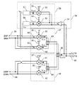
- FIG. 20 is a diagram showing a configuration example of the first unit mixer 39 according to the third embodiment.
- the first unit mixer 39 is a Gilbert cell type differential double-balanced mixer.
- the DC component of the input signal is blocked by the capacitance 61.
- the base voltages of the pair of bipolar transistors 64 and 65 are independently controlled by the differential bias voltage input from the pair of LO leak control terminals 62. That is, the DC component of the positive phase signal of the baseband signal and the DC component of the negative phase signal of the baseband signal are controlled independently of each other.
- LO leakage is caused by frequency conversion of the DC component of the baseband signal. Therefore, the amplitude and polarity of the positive phase signal of LO leak and the amplitude and polarity of the negative phase signal of LO leak are controlled independently.
- the second unit mixer 40 has the same configuration as the first unit mixer 39.
- the configuration of the mixer according to the third embodiment is a configuration in which the feedback circuit 59 is added to the mixer according to the second embodiment. Further, the output terminal of the first bias control circuit 56 is connected to the first LO leak control terminal 49, and the output terminal of the second bias control circuit 57 is connected to the second LO leak control terminal 50. Has been done. That is, the feedback circuit 59 is added, and the first unit mixer 39 and the second unit mixer 40 include a first LO leak control terminal 49 and a second LO leak control terminal 50, respectively.
- the configuration of the mixer other than that is the same as that of the second embodiment.
- the LO leak occurs when each LO wave leaks from the LO input terminal of each unit mixer to the RF signal terminal.
- LO leakage may occur due to the imbalance of the differential circuit in each unit mixer due to the manufacturing variation of each unit mixer.
- the mixer according to the third embodiment When the mixer according to the third embodiment is operated in a state where no signal is input to the first input terminal 33 and the second input terminal 34, the LO leak due to the leakage of the LO wave becomes the second embodiment. It will be canceled in the same way as the mixer. Therefore, in this case, only LO leak occurs due to the manufacturing variation of each unit mixer.
- the first unit mixer 39 outputs the first LO leak from the RF signal terminal of the first unit mixer 39.
- the second unit mixer 40 outputs a second LO leak from the RF signal terminal of the second unit mixer 40.
- the third unit mixer 41 outputs a third LO leak from the RF signal terminal of the third unit mixer 41.
- the fourth unit mixer 42 outputs a fourth LO leak from the RF signal terminal of the fourth unit mixer 42.
- the second synthesizer 43 synthesizes the first LO leak and the second LO leak, and outputs the fifth LO leak.
- the third synthesizer 44 synthesizes the third LO leak and the fourth LO leak, and outputs the sixth LO leak.
- the first synthesizer 45 synthesizes the fifth LO leak and the sixth LO leak.
- the LO leak synthesized by the first synthesizer 45 is distributed in phase to the seventh LO leak and the eighth LO leak.
- the seventh LO leak is output to the amplifier 51.
- the eighth LO leak is output to the outside from the first output terminal 46.
- the amplifier 51 amplifies the 7th LO leak and outputs the amplified 7th LO leak as the 9th LO leak.
- the ninth LO leak is input to the third orthogonal mixer 58 and is distributed in phase to the tenth LO leak and the eleventh LO leak.
- the tenth LO leak is input to the RF signal terminal of the fifth unit mixer 52.
- the eleventh LO leak is input to the RF signal terminal of the sixth unit mixer 53.
- the fifth unit mixer 52 multiplies the LO wave with a phase of 0 ° input from the fifth LO input terminal 54 by the tenth LO leak, and from the baseband signal terminal of the fifth unit mixer 52 to the fifth unit. Twelve signals are output.
- the sixth unit mixer 53 multiplies the LO wave having a phase of 90 ° input from the sixth LO input terminal 55 by the eleventh LO leak, and from the baseband signal terminal of the sixth unit mixer 53 to the thirth. 13 signals are output.
- the first bias control circuit 56 outputs a first bias voltage V B1 corresponding to the magnitude of the input twelfth signal, that is, the signal output from the fifth baseband signal terminal.
- the second bias control circuit 57 outputs a second bias voltage V B2 corresponding to the magnitude of the input thirteenth signal, that is, the signal output from the sixth baseband signal terminal.
- the first bias voltage V B1 is input to the first LO leak control terminal 49 of the first unit mixer 39.
- the second bias voltage V B2 is input to the second LO leak control terminal 50 of the second unit mixer 40.
- FIG. 19 is a diagram showing LO leak of the mixer according to the third embodiment.
- V LO1 is the first LO leak resulting from the first unit mixer 39.
- V LO2 is a second LO leak resulting from the second unit mixer 40.
- V LO3 is a third LO leak resulting from the third unit mixer 41.
- V LO4 is a fourth LO leak resulting from the fourth unit mixer 42.
- V LOOUT is the seventh LO leak after being synthesized by the first synthesizer 45.
- V cont1 is a signal in which LO leak V LOOUT is down-converted by the fifth unit mixer 52, and corresponds to the twelfth LO leak.
- V cont2 is a signal in which LO leak V LOOUT is down-converted by the sixth unit mixer 53, and corresponds to the thirteenth LO leak.
- the LO wave having a phase of 0 ° is represented by cos ⁇ t
- the LO wave having a phase of 90 ° is represented by sin ⁇ t
- the LO wave having a phase of 180 ° is represented by ⁇ cos ⁇ t
- the LO wave having a phase of 270 ° is represented by ⁇ sin ⁇ t.
- the amplitude of the first LO leak V LO1, the amplitude of the second LO leak V LO2 , the amplitude of the third LO leak V LO3 , and the amplitude of the fourth LO leak V LO4 are ⁇ V 1 , ⁇ V 2 , ⁇ V 3 , respectively. Let it be ⁇ V 4 .
- the first LO leak V LO1 , the second LO leak V LO2 , the third LO leak V LO3, and the fourth LO leak V LO4 are according to the following equations (1) to (4). Each is represented.
- V LO1 ⁇ V 1 ⁇ cos ⁇ t... (1)
- V LO2 ⁇ V 2 ⁇ sin ⁇ t... (2)
- V LO3 - ⁇ V 3 ⁇ sin ⁇ t... (3)
- V LO4 ⁇ V 4 ⁇ cos ⁇ t... (4)
- V LOOUT ( ⁇ V 1 - ⁇ V 4 ) ⁇ cos ⁇ t + ( ⁇ V 2- ⁇ V 3 ) ⁇ sin ⁇ t... (5)
- the twelfth LO leak V cont1 and the thirteenth LO leak V cont2 are represented by the following equations (6) and (7), respectively.
- V cont1 Ga ⁇ ( ⁇ V 1 ⁇ ⁇ V 4 ) / 2...
- V cont2 Ga ⁇ ( ⁇ V 2- ⁇ V 3 ) / 2... (9)
- the first bias control circuit 56 outputs the first bias voltage V B1 corresponding to the magnitude of the twelfth LO leak V cont 1 to the first LO leak control terminal 49.
- the DC component of the baseband signal is controlled, and the amplitude ⁇ V 1 and the polarity of the first LO leak V LO 1 are changed.
- the second bias control circuit 57 outputs a second bias voltage V B2 corresponding to the magnitude of the thirteenth LO leak V cont 2 to the second LO leak control terminal 50.
- the correspondence between the magnitude of the twelfth LO leak V cont1 and the first bias voltage V B1 is set in advance so that the feedback control in the feedback circuit 59 becomes a negative feedback control.
- the correspondence between the magnitude of the thirteenth LO leak V cont2 and the second bias voltage V B2 is set in advance so that the feedback control in the feedback circuit 59 becomes a negative feedback control.
- the twelfth LO leak V cont 1 and the first bias voltage V B 1 correspond in advance so that the amplitude ⁇ V 1 of the first LO leak approaches the amplitude ⁇ V 4 of the fourth LO leak. It is attached.
- the thirteenth LO leak V cont 2 and the second bias voltage V B 2 are associated in advance so that the amplitude ⁇ V 2 of the second LO leak approaches the amplitude ⁇ V 3 of the third LO leak. .. Therefore, by this feedback control, the 12th LO leak V cont1 and the 13th LO leak V cont2 converge to 0, respectively, and the 7th LO leak V LOOUT converges to 0.
- the amplitude [Delta] V 1 of the first LO leakage V LO1 is the amplitude [Delta] V 4 of the fourth LO leakage V LO4 equal, and the phase of the first LO leakage V LO1, the fourth LO leakage V LO4 The phase is opposite.
- the amplitude [Delta] V 2 of the second LO leakage V LO2 the amplitude [Delta] V 3 of the third LO leakage V LO3 equal, and the phase of the second LO leakage V LO2, a third LO phase of the leak V LO3 Is in the opposite phase.
- the feedback circuit 59 corrects LO leaks due to manufacturing variations of the first unit mixer 39, the second unit mixer 40, the third unit mixer 41, and the fourth unit mixer 42.
- the first input signal is not input to the first input terminal 33, and the second input signal is not input to the second input terminal 34.
- the feedback circuit 59 is operated.
- the mixer according to the third embodiment corrects LO leakage due to manufacturing variation of each unit mixer by feedback control of the feedback circuit 59.
- the first bias voltage V B1 is determined as the first reference voltage
- the second bias voltage V B2 is determined as the second reference voltage. To do.
- the mixer according to the third embodiment provides feedback when the first input signal is input to the first input terminal 33 and the second input signal is input to the second input terminal 34.
- the operation of the circuit 59 is stopped.
- the output voltage of the first bias control circuit 56 is set to the first reference voltage
- the output voltage of the second bias control circuit 57 is set to the second reference voltage. To do.
- the first bias voltage V B1 is held at the first reference voltage after the LO leak due to the manufacturing variation of each unit mixer is corrected.
- the second bias voltage V B2 is held at the second reference voltage.
- the mixer according to the third embodiment can suppress not only LO leak due to leakage of in-phase signal and LO wave between differential terminals but also LO leak due to manufacturing variation of each unit mixer.
- the baseband signal terminal of the third unit mixer 41 has its polarity reversed and is connected to the second input terminal 34.
- the terminal whose polarity is inverted may be the baseband signal terminal of the first unit mixer 39, the baseband signal terminal of the second unit mixer 40, or the baseband signal of the fourth unit mixer 42. It may be a terminal.
- the RF terminals of the first unit mixer 39, the second unit mixer 40, the third unit mixer 41, the fourth unit mixer 42, the fifth unit mixer 52, and the sixth unit mixer 53 are all simple. It may be a phase.
- the baseband signal terminal and the RF signal terminal are all differential. It was a terminal. However, at least the baseband signal terminal may be a differential terminal.
- the first unit mixer 39 and the second unit mixer 40 are differential double-balanced mixers using Gilbert cells.
- the first unit mixer 39 and the second unit mixer 40 are mixers that can differentially and independently control the LO leak output from the RF signal terminal by controlling the DC component of the baseband signal. , Any configuration may be used.
- the phase of the fifth LO wave is set to 0 °
- the phase of the sixth LO wave is set to 90 °. That is, the fifth LO wave was in phase with the first LO wave, and the sixth LO wave was in phase with the second LO wave.
- the phase of the fifth LO wave may be set to 180 ° and the phase of the sixth LO wave may be set to 270 °. That is, the fifth LO wave may be set to be in phase with the fourth LO wave, and the sixth LO wave may be set to be in phase with the third LO wave.
- the fourth unit mixer 42 includes a first LO leak control terminal
- the third unit mixer 41 includes a second LO leak control terminal.
- the third LO wave oscillator is omitted.
- the fifth LO wave and the sixth LO wave may be oscillated from the first LO wave oscillator.
- the third LO wave oscillator is omitted.
- the fifth LO wave and the sixth LO wave may be oscillated from the second LO wave oscillator.
- the phase of the first LO wave is set to 0 °
- the phase of the second LO wave is set to 90 °.
- the phases of these LO waves need only be orthogonal to each other and are not limited to 0 ° and 90 °.
- the phase of the third LO wave is set to 270 °
- the phase of the fourth LO wave is set to 180 °.
- the phases of these LO waves need only be orthogonal to each other and are not limited to 270 ° and 180 °.
- phase of the LO wave oscillated from the first LO wave oscillator and the phase of the LO wave oscillated from the second LO wave oscillator must be different by 180 °.
- the phase of the first LO wave and the phase of the fourth LO wave are different by 180 °.
- the phase of the first LO wave and the phase of the third LO wave may be different by 180 °.
- the phase of the second LO wave and the phase of the third LO wave are different by 180 °.
- the phase of the second LO wave and the phase of the fourth LO wave may differ by 180 °.
- the 90 ° phase difference distributor may be a 90 ° phase difference distributor or a combination of an in-phase distributor and a 90 ° phase distributor.
- the phases of the LO waves input to the LO input terminals 54 and 55 are set to 0 ° and 90 °, but 180 ° and 270 ° may be used.
- the frequency of the LO wave input to the fifth unit mixer 52 and the sixth unit mixer 53 is the first unit mixer 39, the second unit mixer 40, and the third unit. It was equal to the frequency of the LO wave input to the mixer 41 and the fourth unit mixer 42.
- the frequency of the LO wave input to the fifth unit mixer 52 and the sixth unit mixer 53 is the first unit mixer 39, the second unit mixer 40, the third unit mixer 41, and the fourth unit. It may be different from the frequency of the LO wave input to the mixer 42.
- the frequency of the fifth LO wave is set to a value different from the frequency of the first LO wave
- the frequency of the sixth LO wave is set to a value different from the frequency of the second LO wave. Good.
- the frequency of the fifth LO wave is set to a value different from the frequency of the fourth LO wave
- the frequency of the sixth LO wave is set to a value different from the frequency of the third LO wave. Good.
- the influence of the DC offset component caused by the manufacturing variation of the fifth unit mixer 52 and the sixth unit mixer 53 on the twelfth LO leak V cont1 and the thirteenth LO leak V cont2 is suppressed. be able to.
- the twelfth LO leak V cont1 and the thirteenth LO leak V cont2 are both AC components. Therefore, the first bias control circuit 56 needs to generate a bias voltage such that the amplitude of the AC component of the twelfth LO leak V cont1 is zero. Similarly, the second bias control circuit 57 needs to generate a bias voltage such that the amplitude of the AC component of the thirteenth LO leak V cont2 is zero.
- the phase of the LO wave input to the fifth LO input terminal 54 and the phase of the LO wave input to the sixth LO input terminal 55 were 0 ° and 90 °, respectively. However, it may be 180 ° and 270 °, respectively.
- the amplifier 51 is used as the directional device, but for example, an isolator for RF may be used.
- the amplifier 51 can be used. It may be removed.
- first bias control circuit 56 and the second bias control circuit 57 may include not only an analog circuit but also a digital circuit such as an AD converter.
- the configuration of the mixer shown in FIG. 18 is merely an example, and is not limited thereto.
- the first synthesizer 45, the second synthesizer 43, and the third synthesizer 44 were used as the synthesizer, but these may be composed of one synthesizer. That is, the output signal from the first unit mixer 39, the output signal from the second unit mixer 40, the output signal from the third unit mixer 41, and the output signal from the fourth unit mixer 42 are combined into one synthesizer. May be synthesized by.
- the mixer according to the third embodiment has been used as a transmission mixer, it may be used as a reception mixer.
Abstract
This mixer is provided with a first unit mixer, a second unit mixer, a third unit mixer, and a fourth unit mixer, all having the same configuration, as well as being provided with a first combiner, a second combiner, and a third combiner. The first to fourth unit mixers are each equipped with a differential RF signal terminal. The output of the first unit mixer and the output of the second unit mixer are combined by the second combiner. The output of the third unit mixer and the output of the fourth unit mixer are combined by the third combiner. The output of the second combiner and the output of the third combiner are combined by the first combiner. The output of the third unit mixer is input to the third combiner after inverting the polarity.
Description
本発明は、複数の単位ミクサを有しているミクサに関する。
The present invention relates to a mixer having a plurality of unit mixers.
送信装置に用いられるミクサは、ダイレクトコンバージョン方式またはヘテロダイン方式の通信システムにおいて、ベースバンド信号を所望の周波数帯へアップコンバートする回路から構成されている。その種のミクサは、第1の単位ミクサと、第2の単位ミクサと、第1の合成器とを有する。第1の単位ミクサは、局部発振波を入力とし、Iチャネルのベースバンド信号をアップコンバートする。なお、以下では、局部発振波を、LO(Local Oscillation)波と呼ぶこととする。第2の単位ミクサは、第1の単位ミクサのLO波に対して90°の位相差を有するLO波を入力とし、Qチャネルのベースバンド信号をアップコンバートする。第1の合成器は、第1の単位ミクサの出力信号と第2の単位ミクサの出力信号とを合成する。
The mixer used in the transmitter is composed of a circuit that up-converts a baseband signal to a desired frequency band in a direct conversion system or a heterodyne system communication system. Such mixers have a first unit mixer, a second unit mixer, and a first synthesizer. The first unit mixer takes a locally oscillated wave as an input and up-converts an I-channel baseband signal. In the following, the local oscillator wave will be referred to as an LO (Local Oscillation) wave. The second unit mixer takes an LO wave having a phase difference of 90 ° with respect to the LO wave of the first unit mixer as an input, and up-converts the baseband signal of the Q channel. The first synthesizer synthesizes the output signal of the first unit mixer and the output signal of the second unit mixer.
ミクサは、一般的に、良好な通信を実現するために、出力信号に現れる不要スプリアスの抑制が求められる。
Mixers are generally required to suppress unnecessary spurious emissions that appear in output signals in order to achieve good communication.
従来では、例えば特許文献1または特許文献2に記載の手法により、不要スプリアスを抑制している。
Conventionally, unnecessary spurious is suppressed by, for example, the method described in Patent Document 1 or Patent Document 2.
特許文献1では、通信用半導体集積回路が、送信信号をアップコンバートするミクサに供給する入力信号を生成するための分周回路を有している。分周回路は、局部発振信号を分周することで、当該入力信号を生成する。分周回路は、下段差動トランジスタと上段差動トランジスタとを有するギルバートセル型の回路を用いて構成されている。なお、下段差動トランジスタとして、MOS(Metal-Oxide-Semiconductor)トランジスタが用いられ、上段差動トランジスタとして、バイポーラトランジスタが用いられている。このとき、ミクサの出力には、不要スプリアスが多数発生している。この不要スプリアスを抑制するために、ミクサの入力前段にLPF(Low Pass Filter)が設置されている。
In Patent Document 1, the communication semiconductor integrated circuit has a frequency dividing circuit for generating an input signal to be supplied to a mixer that up-converts a transmission signal. The frequency dividing circuit generates the input signal by dividing the local oscillation signal. The frequency dividing circuit is configured by using a Gilbert cell type circuit having a lower differential transistor and an upper differential transistor. A MOS (Metal-Oxide-Semiconductor) transistor is used as the lower differential transistor, and a bipolar transistor is used as the upper differential transistor. At this time, a large number of unnecessary spurs are generated in the output of the mixer. In order to suppress this unnecessary spurious, an LPF (Low Pass Filter) is installed in front of the input of the mixer.
特許文献2に記載の送信システム半導体集積回路装置は、第一の局発信号を0/90°に位相分配する位相分配手段と、位相分配された局発信号の振幅誤差成分をなくす振幅等化手段と、位相分配された局発信号とベースバンド信号とを掛け合わせて直交変調波を出力する直交変調ミクサと、直交変調波と第二の局発信号と掛け合わせる周波数混合器とを備えている。このとき、直交変調ミクサの出力には、不要スプリアスが多数発生している。この不要スプリアスを抑制するために、直交変調ミクサの入力前段に第一のLPFが設置され、直交変調ミクサの出力後段に第二のLPFが設置されている。
The transmission system semiconductor integrated circuit apparatus described in Patent Document 2 includes a phase partitioning means that phase-distributes the first local signal to 0/90 ° and amplitude equalization that eliminates the amplitude error component of the phase-distributed local signal. A means, a quadrature modulation mixer that outputs a quadrature modulated wave by multiplying a phase-distributed local signal and a baseband signal, and a frequency mixer that multiplies the quadrature modulated wave and a second local signal are provided. There is. At this time, a large number of unnecessary spurs are generated in the output of the quadrature modulation mixer. In order to suppress this unnecessary spurious, the first LPF is installed in the input front stage of the quadrature modulation mixer, and the second LPF is installed in the output rear stage of the quadrature modulation mixer.
特許文献1または特許文献2に記載されているような送信用ミクサの前段には、一般的に、ベースバンド信号を増幅する増幅器が用いられる。しかしながら、増幅器の同相利得除去比(CMRR(Common Mode Rejection Ratio))が低い場合、あるいは、電源と出力端子間のアイソレーションが十分に確保できない場合に、Iチャネルの差動信号とQチャネルの差動信号とに同相信号が含まれる。その場合、差動信号を直交ミクサでアップコンバートした後の負荷の非対称性により、同相信号が不要スプリアスとなって出力端子に生じるという課題があった。
An amplifier that amplifies a baseband signal is generally used in front of a transmission mixer as described in Patent Document 1 or Patent Document 2. However, when the common-mode rejection ratio (CMRR (Common Mode Rejection Ratio)) of the amplifier is low, or when the isolation between the power supply and the output terminal cannot be sufficiently secured, the difference between the differential signal of the I channel and the Q channel. A common-mode signal is included in the dynamic signal. In that case, there is a problem that the in-phase signal becomes unnecessary spurious and occurs at the output terminal due to the asymmetry of the load after up-converting the differential signal with the orthogonal mixer.
本発明は、かかる課題を解消するためになされたものであり、送信用ミクサにおいて、同相信号に起因する不要スプリアスを抑制できるミクサを提供することを目的とする。
The present invention has been made to solve such a problem, and an object of the present invention is to provide a mixer capable of suppressing unnecessary spurious caused by an in-phase signal in a mixer for transmission.
本発明は、ベースバンド信号端子と、LO入力端子と、前記ベースバンド信号端子に入力された信号と前記LO入力端子に入力された局部発振波とを乗算して得られた信号を出力するRF信号端子とを備え、前記ベースバンド信号端子および前記RF信号端子のうちの少なくともいずれか一方が差動端子で構成された、同一構成の第1から第4までの単位ミクサと、第1の入力信号が入力され、前記第1の入力信号を同相分配して、前記第1の単位ミクサの前記ベースバンド信号端子および前記第2の単位ミクサの前記ベースバンド信号端子に同相の信号を与える第1の入力端子と、第2の入力信号が入力され、前記第2の入力信号を同相分配して、前記第3の単位ミクサの前記ベースバンド信号端子および前記第4の単位ミクサの前記ベースバンド信号端子に同相の信号を与える第2の入力端子と、前記第1から前記第4までの単位ミクサの前記RF信号端子から出力される信号を合成する合成器とを備え、前記第1の単位ミクサの前記LO入力端子と前記第2の単位ミクサの前記LO入力端子には、直交関係にある第1の局部発振波および第2の局部発振波がそれぞれ入力され、前記第3の単位ミクサの前記LO入力端子と前記第4の単位ミクサの前記LO入力端子には、直交関係にある第3の局部発振波および第4の局部発振波がそれぞれ入力され、前記第1の局部発振波は、前記第3の局部発振波または前記第4の局部発振波のいずれか一方と180°位相が異なり、前記第2の局部発振波は、前記第3の局部発振波または前記第4の局部発振波のいずれか一方と180°位相が異なり、前記差動端子のうちいずれか1つは、他の前記差動端子に対して、反転した接続関係である、ミクサである。
The present invention outputs a signal obtained by multiplying a baseband signal terminal, an LO input terminal, a signal input to the baseband signal terminal, and a locally oscillating wave input to the LO input terminal. A unit mixer from the first to the fourth having the same configuration, which includes a signal terminal and at least one of the base band signal terminal and the RF signal terminal is a differential terminal, and a first input. A first signal is input, the first input signal is distributed in phase, and a signal having the same phase is given to the baseband signal terminal of the first unit mixer and the baseband signal terminal of the second unit mixer. The input terminal and the second input signal are input, and the second input signal is distributed in phase to the baseband signal terminal of the third unit mixer and the baseband signal of the fourth unit mixer. The first unit mixer includes a second input terminal that gives in-phase signals to the terminals and a synthesizer that synthesizes signals output from the RF signal terminals of the first to fourth unit mixers. A first local oscillation wave and a second local oscillation wave, which are orthogonal to each other, are input to the LO input terminal and the LO input terminal of the second unit mixer, respectively, and the third unit mixer A third local oscillation wave and a fourth local oscillation wave, which are orthogonal to each other, are input to the LO input terminal and the LO input terminal of the fourth unit mixer, respectively, and the first local oscillation wave is the said. The phase of the second local oscillation wave is different from that of either the third local oscillation wave or the fourth local oscillation wave by 180 °, and the second local oscillation wave is the third local oscillation wave or the fourth local oscillation wave. One of the differential terminals has a 180 ° phase difference from that of any one, and one of the differential terminals is a mixer having an inverted connection relationship with the other differential terminal.
本発明のミクサによれば、出力端子に現れる同相信号に起因する不要スプリアスを相殺して抑制できる効果を奏する。
According to the mixer of the present invention, there is an effect that unnecessary spurious caused by the in-phase signal appearing at the output terminal can be offset and suppressed.
以下、図面を用いて、本発明に係るミクサの実施の形態について説明する。
Hereinafter, embodiments of the mixer according to the present invention will be described with reference to the drawings.
実施の形態1.
図1は、本発明の実施の形態1に係るミクサの一構成例を示す図である。本実施の形態1では、送信用ミクサとして使用されるミクサを例に挙げて説明するが、これに限定されるものではない。Embodiment 1.
FIG. 1 is a diagram showing a configuration example of a mixer according to a first embodiment of the present invention. In the first embodiment, a mixer used as a transmission mixer will be described as an example, but the present embodiment is not limited to this.
図1は、本発明の実施の形態1に係るミクサの一構成例を示す図である。本実施の形態1では、送信用ミクサとして使用されるミクサを例に挙げて説明するが、これに限定されるものではない。
FIG. 1 is a diagram showing a configuration example of a mixer according to a first embodiment of the present invention. In the first embodiment, a mixer used as a transmission mixer will be described as an example, but the present embodiment is not limited to this.
本実施の形態1に係るミクサは、第1の入力端子1と、第2の入力端子2と、第1の直交ミクサ15と、第2の直交ミクサ16と、第1の直交ミクサ15の出力信号と第2の直交ミクサ16の出力信号とを合成する第1の合成器13と、第1の出力端子14とを備える。
The mixer according to the first embodiment is the output of the first input terminal 1, the second input terminal 2, the first orthogonal mixer 15, the second orthogonal mixer 16, and the first orthogonal mixer 15. It includes a first synthesizer 13 that synthesizes a signal and an output signal of the second orthogonal mixer 16, and a first output terminal 14.
第1の直交ミクサ15は、第1の単位ミクサ7と、第2の単位ミクサ8と、第2の合成器11とを備えている。第1の単位ミクサ7は、ベースバンド信号端子とRF(Radio Frequency)信号端子とを有するとともに、第1のLO波としての0°のLO波が入力される第1のLO入力端子3を有する。なお、第1の単位ミクサ7のベースバンド信号端子とRF信号端子とは、共に、差動端子から構成されている。第2の単位ミクサ8は、ベースバンド信号端子とRF信号端子とを有するとともに、第2のLO波としての90°のLO波が入力される第2のLO入力端子4を有する。なお、第2の単位ミクサ8のベースバンド信号端子とRF信号端子とは、共に、差動端子から構成されている。第2の合成器11は、第1の単位ミクサ7の出力信号と第2の単位ミクサ8の出力信号とを合成する。第1のLO波および第2のLO波は、いずれも、図示しない第1のLO波発振器から入力される。第1のLO波発振器は、例えば、直交発振器から構成される。
The first orthogonal mixer 15 includes a first unit mixer 7, a second unit mixer 8, and a second synthesizer 11. The first unit mixer 7 has a baseband signal terminal and an RF (Radio Frequency) signal terminal, and also has a first LO input terminal 3 to which a 0 ° LO wave as a first LO wave is input. .. The baseband signal terminal and the RF signal terminal of the first unit mixer 7 are both composed of differential terminals. The second unit mixer 8 has a baseband signal terminal and an RF signal terminal, and also has a second LO input terminal 4 to which a 90 ° LO wave as a second LO wave is input. The baseband signal terminal and the RF signal terminal of the second unit mixer 8 are both composed of differential terminals. The second synthesizer 11 synthesizes the output signal of the first unit mixer 7 and the output signal of the second unit mixer 8. Both the first LO wave and the second LO wave are input from a first LO wave oscillator (not shown). The first LO wave oscillator is composed of, for example, an orthogonal oscillator.
なお、ここでは、ベースバンド信号端子とRF信号端子との両方が差動端子で構成されている例について説明しているが、その場合に限らず、ベースバンド信号端子とRF信号端子との少なくとも一方が差動端子で構成されていればよい。なお、差動端子とは、2つの端子が平行に設けられ、一方の端子には元の信号が入力され、他方の端子には元の信号の極性を反転させた信号が入力される端子のことである。また、第1の単位ミクサ7と第2の単位ミクサ8とは、同一の構成を有している。第1の単位ミクサ7と第2の単位ミクサ8とに与えられるLO波として、ここでは、それぞれ、位相が0°と90°の場合を説明したが、その場合に限らず、互いに直交関係にあるLO波であれば、位相は特に限定されない。
Although an example in which both the baseband signal terminal and the RF signal terminal are configured as differential terminals is described here, not only in that case, at least the baseband signal terminal and the RF signal terminal are described. One of them may be configured as a differential terminal. The differential terminal is a terminal in which two terminals are provided in parallel, the original signal is input to one terminal, and the signal in which the polarity of the original signal is inverted is input to the other terminal. That is. Further, the first unit mixer 7 and the second unit mixer 8 have the same configuration. As LO waves given to the first unit mixer 7 and the second unit mixer 8, the cases where the phases are 0 ° and 90 °, respectively, have been described, but not limited to that case, they are orthogonal to each other. If it is a certain LO wave, the phase is not particularly limited.
第2の直交ミクサ16は、第3の単位ミクサ9と、第4の単位ミクサ10と、第3の合成器12とを備えている。第3の単位ミクサ9は、ベースバンド信号端子とRF信号端子とを有するとともに、第3のLO波としての270°のLO波が入力される第3のLO入力端子5を有している。なお、第3の単位ミクサ9のベースバンド信号端子とRF信号端子とは、共に、差動端子から構成されている。また、第3の単位ミクサ9のRF信号端子は、図1に示すように、極性を反転させて、第3の合成器12に接続されている。第4の単位ミクサ10は、ベースバンド信号端子とRF信号端子とを有するとともに、第4のLO波としての180°のLO波が入力される第4のLO入力端子6を有する。なお、第4の単位ミクサ10のベースバンド信号端子とRF信号端子とは、共に、差動端子から構成されている。第3の合成器12は、第3の単位ミクサ9の出力信号と第4の単位ミクサ10の出力信号とを合成する。第3のLO波および第4のLO波は、いずれも、図示しない第2のLO波発振器から入力される。第2のLO波発振器は、例えば、直交発振器から構成される。
The second orthogonal mixer 16 includes a third unit mixer 9, a fourth unit mixer 10, and a third synthesizer 12. The third unit mixer 9 has a baseband signal terminal and an RF signal terminal, and also has a third LO input terminal 5 to which a 270 ° LO wave as a third LO wave is input. The baseband signal terminal and the RF signal terminal of the third unit mixer 9 are both composed of differential terminals. Further, as shown in FIG. 1, the RF signal terminal of the third unit mixer 9 is connected to the third synthesizer 12 with its polarity reversed. The fourth unit mixer 10 has a baseband signal terminal and an RF signal terminal, and also has a fourth LO input terminal 6 into which a 180 ° LO wave as a fourth LO wave is input. The baseband signal terminal and the RF signal terminal of the fourth unit mixer 10 are both composed of differential terminals. The third synthesizer 12 synthesizes the output signal of the third unit mixer 9 and the output signal of the fourth unit mixer 10. Both the third LO wave and the fourth LO wave are input from a second LO wave oscillator (not shown). The second LO wave oscillator is composed of, for example, an orthogonal oscillator.
なお、ここでは、ベースバンド信号端子とRF信号端子との両方が差動端子で構成されている例について説明しているが、その場合に限らず、ベースバンド信号端子とRF信号端子との少なくとも一方が差動端子で構成されていればよい。また、第3の単位ミクサ9と第4の単位ミクサ10とは同一の構成を有している。ここでは、第1から第4まで単位ミクサ7~10が、すべて、同一の構成を有している場合について説明する。第3の単位ミクサ9と第4の単位ミクサ10とに与えられるLO波として、ここでは、それぞれ、位相が270°と180°の場合を説明したが、その場合に限らず、互いに直交関係にあるLO波であれば、位相は特に限定されない。なお、第1のLO波発振器から発振されるLO波と第2のLO波発振器から発振されるLO波とは、180°位相が異なっている。上記の説明においては、第1の単位ミクサ7に入力されるLO波と第4の単位ミクサ10に入力されるLO波とが180°位相が異なるとして説明したが、第1の単位ミクサ7に入力されるLO波と第3の単位ミクサ9に入力されるLO波とが180°位相が異なる構成としてもよい。また、同様に、第2の単位ミクサ8に入力されるLO波と第3の単位ミクサ9に入力されるLO波とが180°位相が異なるとして説明したが、第2の単位ミクサ8に入力されるLO波と第4の単位ミクサ10に入力されるLO波とが180°位相が異なる構成としてもよい。
Although an example in which both the baseband signal terminal and the RF signal terminal are configured as differential terminals is described here, not only in that case, at least the baseband signal terminal and the RF signal terminal are described. One of them may be configured as a differential terminal. Further, the third unit mixer 9 and the fourth unit mixer 10 have the same configuration. Here, the case where the units 7 to 10 from the first to the fourth have the same configuration will be described. As LO waves given to the third unit mixer 9 and the fourth unit mixer 10, the cases where the phases are 270 ° and 180 °, respectively, have been described, but not limited to this case, they are orthogonal to each other. If it is a certain LO wave, the phase is not particularly limited. The LO wave oscillated from the first LO wave oscillator and the LO wave oscillated from the second LO wave oscillator are 180 ° out of phase. In the above description, the LO wave input to the first unit mixer 7 and the LO wave input to the fourth unit mixer 10 are described as having 180 ° out-of-phase, but the first unit mixer 7 has been described. The LO wave input and the LO wave input to the third unit mixer 9 may be configured to be 180 ° out of phase. Similarly, the LO wave input to the second unit mixer 8 and the LO wave input to the third unit mixer 9 have been described as having 180 ° out-of-phase, but they are input to the second unit mixer 8. The LO wave to be generated and the LO wave input to the fourth unit mixer 10 may have a 180 ° phase difference.
第1の入力端子1に入力された第1の入力信号は、第2の信号と第3の信号とに同相分配され、第1の直交ミクサ15に入力される。第2の信号は、第1の単位ミクサ7のベースバンド信号端子に入力され、第3の信号は、第2の単位ミクサ8のベースバンド信号端子に入力される。
The first input signal input to the first input terminal 1 is distributed in phase to the second signal and the third signal, and is input to the first orthogonal mixer 15. The second signal is input to the baseband signal terminal of the first unit mixer 7, and the third signal is input to the baseband signal terminal of the second unit mixer 8.
第1の単位ミクサ7は、第2の信号と第1のLO入力端子3から入力された0°のLO波とを乗算し、第4の信号をRF信号端子から出力する。
The first unit mixer 7 multiplies the second signal by the 0 ° LO wave input from the first LO input terminal 3, and outputs the fourth signal from the RF signal terminal.
第2の単位ミクサ8は、第3の信号と第2のLO入力端子4から入力された90°のLO波とを乗算し、第5の信号をRF信号端子から出力する。
The second unit mixer 8 multiplies the third signal by the 90 ° LO wave input from the second LO input terminal 4, and outputs the fifth signal from the RF signal terminal.
第2の合成器11は、第4の信号と第5の信号とを合成し、第6の信号を出力する。
The second synthesizer 11 synthesizes the fourth signal and the fifth signal, and outputs the sixth signal.
一方、第2の入力端子2に入力された第2の入力信号は、第7の信号と第8の信号とに同相分配され、第2の直交ミクサ16に入力される。第7の信号は、第3の単位ミクサ9のベースバンド信号端子に入力され、第8の信号は、第4の単位ミクサ10のベースバンド信号端子に入力される。
On the other hand, the second input signal input to the second input terminal 2 is distributed in phase to the seventh signal and the eighth signal, and is input to the second orthogonal mixer 16. The seventh signal is input to the baseband signal terminal of the third unit mixer 9, and the eighth signal is input to the baseband signal terminal of the fourth unit mixer 10.
第3の単位ミクサ9は、第7の信号と第3のLO入力端子5から入力された270°のLO波とを乗算し、RF信号端子を反転させて、第9の信号を出力する。
The third unit mixer 9 multiplies the seventh signal by the 270 ° LO wave input from the third LO input terminal 5, inverts the RF signal terminal, and outputs the ninth signal.
第4の単位ミクサ10は、第8の信号と第4のLO入力端子6から入力された180°のLO波とを乗算し、第10の信号をRF信号端子から出力する。
The fourth unit mixer 10 multiplies the eighth signal by the 180 ° LO wave input from the fourth LO input terminal 6, and outputs the tenth signal from the RF signal terminal.
第3の合成器12は、第9の信号と第10の信号とを合成し、第11の信号を出力する。
The third synthesizer 12 synthesizes the ninth signal and the tenth signal, and outputs the eleventh signal.
第1の合成器13は、第6の信号と第11の信号とを合成し、第1の出力端子14から外部に出力する。
The first synthesizer 13 synthesizes the sixth signal and the eleventh signal, and outputs the sixth signal to the outside from the first output terminal 14.
このように、本実施の形態1では、直交ミクサ15,16が、同一構成の4つの単位ミクサ7~10で構成されている。また、それら4つの単位ミクサ、すなわち、第1の単位ミクサ7、第2の単位ミクサ8、第3の単位ミクサ9、第4の単位ミクサ10に対して、90°の位相差のある4相のLO波、すなわち、0°、90°、180°、270°のLO波がそれぞれ用いられている。また、第1の合成器13、第2の合成器11、および、第3の合成器12を設けることで、第1の直交ミクサ15および第2の直交ミクサ16の出力信号が合成されている。また、270°のLO波を入力する第3の単位ミクサ9の出力は、極性を反転させて、後段の第3の合成器12に接続されている。
As described above, in the first embodiment, the orthogonal mixers 15 and 16 are composed of four unit mixers 7 to 10 having the same configuration. Further, there are four phases having a phase difference of 90 ° with respect to these four unit mixers, that is, the first unit mixer 7, the second unit mixer 8, the third unit mixer 9, and the fourth unit mixer 10. LO waves, that is, LO waves of 0 °, 90 °, 180 °, and 270 ° are used, respectively. Further, by providing the first synthesizer 13, the second synthesizer 11, and the third synthesizer 12, the output signals of the first orthogonal mixer 15 and the second orthogonal mixer 16 are synthesized. .. Further, the output of the third unit mixer 9 for inputting the LO wave of 270 ° has its polarity reversed and is connected to the third synthesizer 12 in the subsequent stage.
なお、図1に示した、第1の直交ミクサ15、第2の直交ミクサ16、第1の合成器13、第1の単位ミクサ7、第2の単位ミクサ8、第3の単位ミクサ9、第4の単位ミクサ10、第2の合成器11、および、第3の合成器12の構成は、単なる一例であって、これらに限定されるものではなく、他の構成のものを使用してもよいことは言うまでもない。また、図1においては、3つの合成器11~13を設けているが、1つの合成器で4つの単位ミクサ7~10の出力を合成するようにしてもよい。
The first orthogonal mixer 15, the second orthogonal mixer 16, the first synthesizer 13, the first unit mixer 7, the second unit mixer 8, the third unit mixer 9, and the like shown in FIG. The configurations of the fourth unit mixer 10, the second synthesizer 11, and the third synthesizer 12 are merely examples, and are not limited thereto, and other configurations may be used. Needless to say, it's good. Further, in FIG. 1, three synthesizers 11 to 13 are provided, but one synthesizer may synthesize the outputs of the four unit mixers 7 to 10.
以下、図2~図7を用いて、本実施の形態1に係るミクサの動作について説明する。
Hereinafter, the operation of the mixer according to the first embodiment will be described with reference to FIGS. 2 to 7.
図2は、本実施の形態1に係るIチャネルにおける差動信号の位相関係を示す図である。第4の信号の振幅および第5の信号の振幅を共にVIとし、第6の信号の振幅をVI’とすると、第6の信号の位相および振幅は、図2中の符号Aに示されたベクトル図によって表される。ベクトル図には、アッパーローカルの場合とローワーローカルの場合とがそれぞれ示されている。なお、アッパーローカルとは、第1から第4までの各LO波の周波数が、RF信号の周波数よりも高く設定されている状態を表す語である。ローワーローカルとは、第1から第4までの各LO波の周波数が、RF信号の周波数よりも低く設定されている状態を表す語である。また、第4の信号、第5の信号および第6の信号の各位相および各振幅は、以下の通りである。
FIG. 2 is a diagram showing a phase relationship of differential signals in the I channel according to the first embodiment. The amplitude of the amplitude and the fifth signal of the fourth signal are both V I, when the amplitude of the sixth signal and V I ', the phase and amplitude of the sixth signal, shown by reference numeral A in FIG. 2 It is represented by a vector diagram. The vector diagram shows the upper local case and the lower local case, respectively. The upper local is a word indicating a state in which the frequency of each of the first to fourth LO waves is set higher than the frequency of the RF signal. The lower local is a word indicating a state in which the frequency of each of the first to fourth LO waves is set lower than the frequency of the RF signal. The phases and amplitudes of the fourth signal, the fifth signal, and the sixth signal are as follows.
<アッパーローカル>
信号 位相 振幅
第4の信号 0° VI
第5の信号 90° VI
第6の信号 45° VI’
<ローワーローカル>
信号 位相 振幅
第4の信号 0° VI
第5の信号 270° VI
第6の信号 315° VI’ <Upper Local>
Signal phase amplitude fourth signal 0 ° V I
Fifth signal 90 ° V I
Sixth signal 45 ° V I '
<Lower local>
Signal phase amplitude fourth signal 0 ° V I
Fifth signal 270 ° V I
Sixth signal 315 ° V I '
信号 位相 振幅
第4の信号 0° VI
第5の信号 90° VI
第6の信号 45° VI’
<ローワーローカル>
信号 位相 振幅
第4の信号 0° VI
第5の信号 270° VI
第6の信号 315° VI’ <Upper Local>
Signal phase amplitude fourth signal 0 ° V I
Fifth signal 90 ° V I
Sixth signal 45 ° V I '
<Lower local>
Signal phase amplitude fourth signal 0 ° V I
Fifth signal 270 ° V I
Sixth signal 315 ° V I '
図3は、本実施の形態1に係るQチャネルにおける差動信号の位相関係を示す図である。第9の信号の振幅および第10の信号の振幅を共にVQとし、第11の信号の振幅をVQ’とすると、第11の信号の位相および振幅は、図3中の符号Bに示されたベクトル図によって表される。ベクトル図には、アッパーローカルの場合とローワーローカルの場合とがそれぞれ示されている。また、第9の信号、第10の信号および第11の信号の各位相および各振幅は、以下の通りである。
FIG. 3 is a diagram showing a phase relationship of differential signals in the Q channel according to the first embodiment. Assuming that the amplitude of the ninth signal and the amplitude of the tenth signal are both V Q and the amplitude of the eleventh signal is V Q ', the phase and amplitude of the eleventh signal are shown by reference numeral B in FIG. It is represented by a vector diagram. The vector diagram shows the upper local case and the lower local case, respectively. The phases and amplitudes of the ninth signal, the tenth signal, and the eleventh signal are as follows.
<アッパーローカル>
信号 位相 振幅
第9の信号 90° VQ
第10の信号 180° VQ
第11の信号 135° VQ’
<ローワーローカル>
信号 位相 振幅
第9の信号 270° VQ
第10の信号 180° VQ
第11の信号 225° VQ’ <Upper Local>
Signal Phase Amplitude Ninth Signal 90 ° V Q
10th signal 180 ° V Q
11th signal 135 ° V Q '
<Lower local>
Signal Phase Amplitude Ninth Signal 270 ° V Q
10th signal 180 ° V Q
11th signal 225 ° V Q '
信号 位相 振幅
第9の信号 90° VQ
第10の信号 180° VQ
第11の信号 135° VQ’
<ローワーローカル>
信号 位相 振幅
第9の信号 270° VQ
第10の信号 180° VQ
第11の信号 225° VQ’ <Upper Local>
Signal Phase Amplitude Ninth Signal 90 ° V Q
10th signal 180 ° V Q
11th signal 135 ° V Q '
<Lower local>
Signal Phase Amplitude Ninth Signal 270 ° V Q
10th signal 180 ° V Q
11th signal 225 ° V Q '
図4は、本実施の形態1に係る合成後における差動信号の位相関係を示す図である。第1の出力端子14における第6の信号および第11の信号の位相および振幅は、図4中の符号Cに示されたベクトル図によって表される。ベクトル図には、アッパーローカルの場合とローワーローカルの場合とがそれぞれ示されている。また、第6の信号および第11の信号の各位相および各振幅は、以下の通りである。
FIG. 4 is a diagram showing the phase relationship of the differential signal after synthesis according to the first embodiment. The phase and amplitude of the sixth signal and the eleventh signal at the first output terminal 14 are represented by the vector diagram indicated by reference numeral C in FIG. The vector diagram shows the upper local case and the lower local case, respectively. Further, each phase and each amplitude of the sixth signal and the eleventh signal are as follows.
<アッパーローカル>
信号 位相 振幅
第6の信号 45° VI’
第11の信号 135° VQ’
<ローワーローカル>
信号 位相 振幅
第6の信号 315° VI’
第11の信号 225° VQ’
このように、Iチャネルの信号とQチャネルの信号が直交するため、図1に示した本実施の形態1に係るミクサは、直交ミクサとして動作する。 <Upper Local>
Signal phase amplitude sixth signal 45 ° V I '
11th signal 135 ° V Q '
<Lower local>
Signal phase amplitude sixth signal 315 ° V I '
11th signal 225 ° V Q '
Since the I-channel signal and the Q-channel signal are orthogonal to each other in this way, the mixer according to the first embodiment shown in FIG. 1 operates as an orthogonal mixer.
信号 位相 振幅
第6の信号 45° VI’
第11の信号 135° VQ’
<ローワーローカル>
信号 位相 振幅
第6の信号 315° VI’
第11の信号 225° VQ’
このように、Iチャネルの信号とQチャネルの信号が直交するため、図1に示した本実施の形態1に係るミクサは、直交ミクサとして動作する。 <Upper Local>
Signal phase amplitude sixth signal 45 ° V I '
11th signal 135 ° V Q '
<Lower local>
Signal phase amplitude sixth signal 315 ° V I '
11th signal 225 ° V Q '
Since the I-channel signal and the Q-channel signal are orthogonal to each other in this way, the mixer according to the first embodiment shown in FIG. 1 operates as an orthogonal mixer.
図5は、本実施の形態1に係るIチャネルにおける同相信号の位相関係を示す図である。第4の信号および第5の信号にそれぞれ生じる差動間の同相信号の振幅を共にVcmとし、第6の信号に生じる差動間の同相信号の振幅をVcm’とすると、第6の信号に生じる差動間の同相信号の位相および振幅は、図5中の符号Dに示されたベクトル図によって表される。ベクトル図には、アッパーローカルの場合とローワーローカルの場合とがそれぞれ示されている。また、第4の信号に生じる差動間の同相信号、第5の信号に生じる差動間の同相信号および第6の信号に生じる差動間の同相信号の各位相および各振幅は、以下の通りである。
FIG. 5 is a diagram showing a phase relationship of in-phase signals in the I channel according to the first embodiment. The amplitude of the phase signal between the differential occurring respectively in the fourth signal and the fifth signal and both V cm, when the amplitude of the phase signal between the differential occurring in the sixth signal and V cm ', the The phase and amplitude of the differential in-phase signals generated in signal 6 are represented by the vector diagram shown by reference numeral D in FIG. The vector diagram shows the upper local case and the lower local case, respectively. Further, the phases and amplitudes of the differential in-phase signal generated in the fourth signal, the differential-phase in-phase signal generated in the fifth signal, and the differential-phase in-phase signal generated in the sixth signal are , Is as follows.
<アッパーローカル>
信号 位相 振幅
第4の信号に生じる差動間の同相信号 0° Vcm
第5の信号に生じる差動間の同相信号 90° Vcm
第6の信号に生じる差動間の同相信号 45° Vcm’
<ローワーローカル>
信号 位相 振幅
第4の信号に生じる差動間の同相信号 0° Vcm
第5の信号に生じる差動間の同相信号 270° Vcm
第6の信号に生じる差動間の同相信号 315° Vcm’ <Upper Local>
Signal Phase Amplitude Common-mode rejection signal between differentials generated in the fourth signal 0 ° V cm
Common-mode rejection between differentials generated in the fifth signal 90 ° V cm
Common-mode rejection between differentials occurring in thesixth signal 45 ° V cm '
<Lower local>
Signal Phase Amplitude Common-mode rejection signal between differentials generated in the fourth signal 0 ° V cm
Common-mode rejection signal between differentials generated in the fifth signal 270 ° V cm
Common-mode rejection between differentials generated in the sixth signal 315 ° V cm '
信号 位相 振幅
第4の信号に生じる差動間の同相信号 0° Vcm
第5の信号に生じる差動間の同相信号 90° Vcm
第6の信号に生じる差動間の同相信号 45° Vcm’
<ローワーローカル>
信号 位相 振幅
第4の信号に生じる差動間の同相信号 0° Vcm
第5の信号に生じる差動間の同相信号 270° Vcm
第6の信号に生じる差動間の同相信号 315° Vcm’ <Upper Local>
Signal Phase Amplitude Common-mode rejection signal between differentials generated in the fourth signal 0 ° V cm
Common-mode rejection between differentials generated in the fifth signal 90 ° V cm
Common-mode rejection between differentials occurring in the
<Lower local>
Signal Phase Amplitude Common-mode rejection signal between differentials generated in the fourth signal 0 ° V cm
Common-mode rejection signal between differentials generated in the fifth signal 270 ° V cm
Common-mode rejection between differentials generated in the sixth signal 315 ° V cm '
図6は、本実施の形態1に係るQチャネルにおける同相信号の位相関係を示す図である。第9の信号および第10の信号にそれぞれ生じる差動間の同相信号の振幅を共にVcmとし、第11の信号に生じる差動間の同相信号の振幅をVcm’とすると、第11の信号に生じる差動間の同相信号の位相および振幅は、図6中の符号Eに示されたベクトル図によって表される。ベクトル図には、アッパーローカルの場合とローワーローカルの場合とがそれぞれ示されている。また、第9の信号に生じる差動間の同相信号、第10の信号に生じる差動間の同相信号および第11の信号に生じる差動間の同相信号の各位相および各振幅は、以下の通りである。
FIG. 6 is a diagram showing a phase relationship of in-phase signals in the Q channel according to the first embodiment. Assuming that the amplitudes of the differential in-phase signals generated in the ninth signal and the tenth signal are both V cm and the amplitudes of the differential-phase signals generated in the eleventh signal are V cm '. The phase and amplitude of the differential in-phase signals generated in the 11 signals are represented by the vector diagram shown by reference numeral E in FIG. The vector diagram shows the upper local case and the lower local case, respectively. Further, the phases and amplitudes of the differential in-phase signal generated in the ninth signal, the differential-phase in-phase signal generated in the tenth signal, and the differential-phase in-phase signal generated in the eleventh signal are , Is as follows.
<アッパーローカル>
信号 位相 振幅
第9の信号に生じる差動間の同相信号 270° Vcm
第10の信号に生じる差動間の同相信号 180° Vcm
第11の信号に生じる差動間の同相信号 225° Vcm’
<ローワーローカル>
信号 位相 振幅
第9の信号に生じる差動間の同相信号 90° Vcm
第10の信号に生じる差動間の同相信号 180° Vcm
第11の信号に生じる差動間の同相信号 135° Vcm’ <Upper Local>
Signal Phase Amplitude Common-mode rejection signal between differentials generated in the ninth signal 270 ° V cm
Common-mode rejection between differentials generated in the tenth signal 180 ° V cm
Common-mode rejection signal between differentials generated in the eleventh signal 225 ° V cm '
<Lower local>
Signal Phase Amplitude Common-mode rejection signal between differentials generated in the ninth signal 90 ° V cm
Common-mode rejection between differentials generated in the tenth signal 180 ° V cm
Common-mode rejection between differentials generated in the eleventh signal 135 ° V cm '
信号 位相 振幅
第9の信号に生じる差動間の同相信号 270° Vcm
第10の信号に生じる差動間の同相信号 180° Vcm
第11の信号に生じる差動間の同相信号 225° Vcm’
<ローワーローカル>
信号 位相 振幅
第9の信号に生じる差動間の同相信号 90° Vcm
第10の信号に生じる差動間の同相信号 180° Vcm
第11の信号に生じる差動間の同相信号 135° Vcm’ <Upper Local>
Signal Phase Amplitude Common-mode rejection signal between differentials generated in the ninth signal 270 ° V cm
Common-mode rejection between differentials generated in the tenth signal 180 ° V cm
Common-mode rejection signal between differentials generated in the eleventh signal 225 ° V cm '
<Lower local>
Signal Phase Amplitude Common-mode rejection signal between differentials generated in the ninth signal 90 ° V cm
Common-mode rejection between differentials generated in the tenth signal 180 ° V cm
Common-mode rejection between differentials generated in the eleventh signal 135 ° V cm '
図7は実施の形態1に係る合成後における同相信号の位相関係を示す図である。第1の出力端子14における第6の信号および第11の信号の位相および振幅は、図7中の符号Fに示されたベクトル図によって表される。ベクトル図には、アッパーローカルの場合とローワーローカルの場合とがそれぞれ示されている。また、第6の信号および第11の信号の各位相および各振幅は、以下の通りである。
FIG. 7 is a diagram showing a phase relationship of in-phase signals after synthesis according to the first embodiment. The phase and amplitude of the sixth signal and the eleventh signal at the first output terminal 14 are represented by the vector diagram indicated by reference numeral F in FIG. The vector diagram shows the upper local case and the lower local case, respectively. Further, each phase and each amplitude of the sixth signal and the eleventh signal are as follows.
<アッパーローカル>
信号 位相 振幅
第6の信号 45° Vcm’
第11の信号 225° Vcm’
<ローワーローカル>
信号 位相 振幅
第6の信号 315° Vcm’
第11の信号 135° Vcm’
このように、本実施の形態1に係るミクサにおいては、Iチャネルの同相信号とQチャネルの同相信号が同じ振幅かつ逆相で合成されるため、同相信号が打ち消される。 <Upper Local>
Signal Phase Amplitude 6th signal 45 ° V cm '
11th signal 225 ° V cm '
<Lower local>
Signal Phase Amplitude 6th Signal 315 ° V cm '
11th signal 135 ° V cm '
As described above, in the mixer according to the first embodiment, the in-phase signal of the I channel and the in-phase signal of the Q channel are combined with the same amplitude and opposite phase, so that the in-phase signal is canceled.
信号 位相 振幅
第6の信号 45° Vcm’
第11の信号 225° Vcm’
<ローワーローカル>
信号 位相 振幅
第6の信号 315° Vcm’
第11の信号 135° Vcm’
このように、本実施の形態1に係るミクサにおいては、Iチャネルの同相信号とQチャネルの同相信号が同じ振幅かつ逆相で合成されるため、同相信号が打ち消される。 <Upper Local>
Signal Phase Amplitude 6th signal 45 ° V cm '
11th signal 225 ° V cm '
<Lower local>
Signal Phase Amplitude 6th Signal 315 ° V cm '
11th signal 135 ° V cm '
As described above, in the mixer according to the first embodiment, the in-phase signal of the I channel and the in-phase signal of the Q channel are combined with the same amplitude and opposite phase, so that the in-phase signal is canceled.
このように、本実施の形態1では、直交ミクサ15,16が、同一構成の4つの単位ミクサ7~10で構成されている。また、180°位相が異なる第1のLO波発振器と第2のLO波発振器とを用いて、それら4つの単位ミクサ、すなわち、第1の単位ミクサ7、第2の単位ミクサ8、第3の単位ミクサ9、第4の単位ミクサ10のそれぞれに対して、90°の位相差のある4相のLO波をそれぞれ入力している。また、第1の合成器13、第2の合成器11、および、第3の合成器12を設けることで、第1の直交ミクサ15および第2の直交ミクサ16の出力信号が合成され、図7に示すように、同相信号成分が打ち消されている。すなわち、0°と90°のLO波で動作する第1の直交ミクサ15の出力と、第1の直交ミクサ15に対して逆相のLO波である180°と270°のLO波で動作する第2の直交ミクサ16の出力とを合成することで、出力信号をキャンセルしている。但し、単に逆相のLO波を用いただけでは、差動信号と同相信号の両方がキャンセルされてしまうので、本実施の形態1では、1箇所の差動端子だけを反転させて第3の合成器12に接続している。こうすることで、差動端子を反転した部分の前後で、差動信号の極性が反転し、同相信号の極性はそのままとなる。そのため、差動信号に関しては通常のミクサと同等の信号が得られ、同相信号のみを打ち消すことができる。結果、本構成により電源ノイズ等の同相成分が、差動入力に混入することで生じる不要スプリアスを抑制することができる。
As described above, in the first embodiment, the orthogonal mixers 15 and 16 are composed of four unit mixers 7 to 10 having the same configuration. Further, by using the first LO wave oscillator and the second LO wave oscillator having 180 ° phases different from each other, the four unit mixers, that is, the first unit mixer 7, the second unit mixer 8, and the third unit mixer A four-phase LO wave having a phase difference of 90 ° is input to each of the unit mixer 9 and the fourth unit mixer 10. Further, by providing the first synthesizer 13, the second synthesizer 11, and the third synthesizer 12, the output signals of the first orthogonal mixer 15 and the second orthogonal mixer 16 are synthesized. As shown in 7, the in-phase signal component is canceled. That is, it operates with the output of the first orthogonal mixer 15 operating in the LO wave of 0 ° and 90 °, and the LO wave of 180 ° and 270 ° which is the LO wave having the opposite phase to the first orthogonal mixer 15. The output signal is canceled by synthesizing the output of the second orthogonal mixer 16. However, simply using the LO wave of the opposite phase cancels both the differential signal and the in-phase signal. Therefore, in the first embodiment, only one differential terminal is inverted and the third differential terminal is inverted. It is connected to the synthesizer 12. By doing so, the polarity of the differential signal is inverted before and after the portion where the differential terminal is inverted, and the polarity of the in-phase signal remains the same. Therefore, as for the differential signal, a signal equivalent to that of a normal mixer can be obtained, and only the in-phase signal can be canceled. As a result, this configuration can suppress unnecessary spurious generated by mixing in-phase components such as power supply noise into the differential input.
上記の理由により、本実施の形態1で説明した上記の構成を用いることで、差動間の同相信号を打ち消すことが可能なミクサを構成することができる。また、IチャネルとQチャネルとの位相関係が変わるが、第1、第2、第3、第4の単位ミクサ7~10のうちのいずれの単位ミクサの差動端子から構成されたRF信号端子を反転して接続した場合でも同様の動作を実現することができる。また、第1、第2、第3、第4の単位ミクサ7~10は同じ構成であれば、ベースバンド信号端子は単相でも良い。さらに、本実施の形態1において、第1の入力端子1および第2の入力端子2の前段に、90°位相差分配部を設けるようにすれば、本実施の形態1に係るミクサを、イメージリジェクションミクサとして動作させることも可能である。すなわち、第3の入力信号を90°位相差分配部を入力する。これにより、90°位相差分配部が、第3の入力信号から、第1の入力端子1に入力する第1の入力信号と第2の入力端子2に入力する第2の信号とを生成する。なお、90°位相差分配部は、例えば、90°位相差分配器と90°移相器とから構成してもよく、あるいは、同相分配器と90°移相器とから構成してもよい。
For the above reason, by using the above configuration described in the first embodiment, it is possible to configure a mixer capable of canceling in-phase signals between differentials. Further, although the phase relationship between the I channel and the Q channel changes, the RF signal terminal is composed of the differential terminal of any of the first, second, third, and fourth unit mixers 7 to 10. The same operation can be realized even when the above is inverted and connected. Further, the baseband signal terminal may be single-phase as long as the first, second, third, and fourth unit mixers 7 to 10 have the same configuration. Further, in the first embodiment, if a 90 ° phase difference distribution unit is provided in front of the first input terminal 1 and the second input terminal 2, the mixer according to the first embodiment can be imaged. It is also possible to operate as a rejection mixer. That is, the 90 ° phase difference distribution unit inputs the third input signal. As a result, the 90 ° phase difference distribution unit generates, from the third input signal, a first input signal input to the first input terminal 1 and a second signal input to the second input terminal 2. .. The 90 ° phase difference distributor may be composed of, for example, a 90 ° phase difference distributor and a 90 ° phase shifter, or may be composed of an in-phase distributor and a 90 ° phase shifter.
実施の形態2.
図8は、本発明の実施の形態2に係るミクサの一構成例を示す図である。本実施の形態2では、送信用ミクサとして使用されるミクサを例に挙げて説明するが、これに限定されるものではない。Embodiment 2.
FIG. 8 is a diagram showing a configuration example of a mixer according to a second embodiment of the present invention. In the second embodiment, a mixer used as a transmission mixer will be described as an example, but the present invention is not limited to this.
図8は、本発明の実施の形態2に係るミクサの一構成例を示す図である。本実施の形態2では、送信用ミクサとして使用されるミクサを例に挙げて説明するが、これに限定されるものではない。
FIG. 8 is a diagram showing a configuration example of a mixer according to a second embodiment of the present invention. In the second embodiment, a mixer used as a transmission mixer will be described as an example, but the present invention is not limited to this.
本実施の形態2に係るミクサは、第1の入力端子17と、第2の入力端子18と、第1の直交ミクサ31と、第2の直交ミクサ32と、第1の直交ミクサ31の出力信号と第2の直交ミクサ32の出力信号とを合成する第1の合成器29と、第1の出力端子30とを備える。
The mixer according to the second embodiment is the output of the first input terminal 17, the second input terminal 18, the first orthogonal mixer 31, the second orthogonal mixer 32, and the first orthogonal mixer 31. It includes a first synthesizer 29 that synthesizes a signal and an output signal of the second orthogonal mixer 32, and a first output terminal 30.
第1の直交ミクサ31は、第1の単位ミクサ23と、第2の単位ミクサ24と、第2の合成器27とを備えている。第1の単位ミクサ23は、ベースバンド信号端子とRF信号端子とを有するとともに、第1のLO波としての0°のLO波が入力される第1のLO入力端子19を有する。なお、第1の単位ミクサ23のベースバンド信号端子とRF信号端子とは、共に、差動端子から構成されている。第2の単位ミクサ24は、ベースバンド信号端子とRF信号端子とを有するとともに、第2のLO波としての90°のLO波が入力される第2のLO入力端子20を有する。なお、第2の単位ミクサ24のベースバンド信号端子とRF信号端子とは、共に、差動端子から構成されている。第2の合成器27は、第1の単位ミクサ23の出力信号と第2の単位ミクサ24の出力信号とを合成する。第1のLO波および第2のLO波は、いずれも、図示しない第1のLO波発振器から入力される。第1のLO波発振器は、例えば、直交発振器から構成される。
The first orthogonal mixer 31 includes a first unit mixer 23, a second unit mixer 24, and a second synthesizer 27. The first unit mixer 23 has a baseband signal terminal and an RF signal terminal, and also has a first LO input terminal 19 into which a 0 ° LO wave as a first LO wave is input. The baseband signal terminal and the RF signal terminal of the first unit mixer 23 are both composed of differential terminals. The second unit mixer 24 has a baseband signal terminal and an RF signal terminal, and also has a second LO input terminal 20 into which a 90 ° LO wave as a second LO wave is input. The baseband signal terminal and the RF signal terminal of the second unit mixer 24 are both composed of differential terminals. The second synthesizer 27 synthesizes the output signal of the first unit mixer 23 and the output signal of the second unit mixer 24. Both the first LO wave and the second LO wave are input from a first LO wave oscillator (not shown). The first LO wave oscillator is composed of, for example, an orthogonal oscillator.
なお、ここでは、ベースバンド信号端子とRF信号端子との両方が差動端子で構成されている例について説明しているが、その場合に限らず、ベースバンド信号端子とRF信号端子との少なくとも一方が差動端子で構成されていればよい。また、第1の単位ミクサ23と第2の単位ミクサ24とは、同一の構成を有している。第1の単位ミクサ23と第2の単位ミクサ24とに与えられるLO波として、ここでは、それぞれ、位相が0°と90°の場合を説明したが、その場合に限らず、互いに直交関係にあるLO波であれば、位相は特に限定されない。
Although an example in which both the baseband signal terminal and the RF signal terminal are configured as differential terminals is described here, not only in that case, at least the baseband signal terminal and the RF signal terminal are described. One of them may be configured as a differential terminal. Further, the first unit mixer 23 and the second unit mixer 24 have the same configuration. As LO waves given to the first unit mixer 23 and the second unit mixer 24, the cases where the phases are 0 ° and 90 °, respectively, have been described, but not limited to this case, they are orthogonal to each other. If it is a certain LO wave, the phase is not particularly limited.
第2の直交ミクサ32は、第3の単位ミクサ25と、第4の単位ミクサ26と、第3の合成器28とを備えている。第3の単位ミクサ25は、ベースバンド信号端子とRF信号端子とを有するとともに、第3のLO波としての270°のLO波が入力される第3のLO入力端子21を有している。なお、第3の単位ミクサ25のベースバンド信号端子とRF信号端子とは、共に、差動端子から構成されている。また、第3の単位ミクサ25のベースバンド信号端子は、反転して、第2の入力端子18に接続されている。第4の単位ミクサ26は、ベースバンド信号端子とRF信号端子とを有するとともに、第4のLO波としての180°のLO波が入力される第4のLO入力端子22を有する。なお、第4の単位ミクサ26のベースバンド信号端子とRF信号端子とは、共に、差動端子から構成されている。第3の合成器28は、第3の単位ミクサ25の出力信号と第4の単位ミクサ26の出力信号とを合成する。第3のLO波および第4のLO波は、いずれも、図示しない第2のLO波発振器から入力される。第2のLO波発振器は、例えば、直交発振器から構成される。
The second orthogonal mixer 32 includes a third unit mixer 25, a fourth unit mixer 26, and a third synthesizer 28. The third unit mixer 25 has a baseband signal terminal and an RF signal terminal, and also has a third LO input terminal 21 into which a 270 ° LO wave as a third LO wave is input. The baseband signal terminal and the RF signal terminal of the third unit mixer 25 are both composed of differential terminals. Further, the baseband signal terminal of the third unit mixer 25 is inverted and connected to the second input terminal 18. The fourth unit mixer 26 has a baseband signal terminal and an RF signal terminal, and also has a fourth LO input terminal 22 into which a 180 ° LO wave as a fourth LO wave is input. The baseband signal terminal and the RF signal terminal of the fourth unit mixer 26 are both composed of differential terminals. The third synthesizer 28 synthesizes the output signal of the third unit mixer 25 and the output signal of the fourth unit mixer 26. Both the third LO wave and the fourth LO wave are input from a second LO wave oscillator (not shown). The second LO wave oscillator is composed of, for example, an orthogonal oscillator.
なお、ここでは、ベースバンド信号端子とRF信号端子との両方が差動端子で構成されている例について説明しているが、その場合に限らず、ベースバンド信号端子とRF信号端子との少なくとも一方が差動端子で構成されていればよい。また、第3の単位ミクサ25と第4の単位ミクサ26とは同一の構成を有している。ここでは、第1から第4まで単位ミクサ23~26が、すべて、同一の構成を有している場合について説明する。第3の単位ミクサ25と第4の単位ミクサ26とに与えられるLO波として、ここでは、それぞれ、位相が270°と180°の場合を説明したが、その場合に限らず、互いに直交関係にあるLO波であれば、位相は特に限定されない。なお、第1のLO波発振器から発振されるLO波と第2のLO波発振器から発振されるLO波とは、180°位相が異なっている。上記の説明においては、第1の単位ミクサ23に入力されるLO波と第4の単位ミクサ26に入力されるLO波とが180°位相が異なるとして説明したが、第1の単位ミクサ23に入力されるLO波と第3の単位ミクサ25に入力されるLO波とが180°位相が異なる構成としてもよい。また、同様に、第2の単位ミクサ24に入力されるLO波と第3の単位ミクサ25に入力されるLO波とが180°位相が異なるとして説明したが、第2の単位ミクサ24に入力されるLO波と第4の単位ミクサ26に入力されるLO波とが180°位相が異なる構成としてもよい。
Although an example in which both the baseband signal terminal and the RF signal terminal are configured as differential terminals is described here, not only in that case, at least the baseband signal terminal and the RF signal terminal are described. One of them may be configured as a differential terminal. Further, the third unit mixer 25 and the fourth unit mixer 26 have the same configuration. Here, a case where the units mixers 23 to 26 from the first to the fourth have the same configuration will be described. As LO waves given to the third unit mixer 25 and the fourth unit mixer 26, the cases where the phases are 270 ° and 180 °, respectively, have been described, but not limited to this case, they are orthogonal to each other. If it is a certain LO wave, the phase is not particularly limited. The LO wave oscillated from the first LO wave oscillator and the LO wave oscillated from the second LO wave oscillator are 180 ° out of phase. In the above description, the LO wave input to the first unit mixer 23 and the LO wave input to the fourth unit mixer 26 are described as having 180 ° out-of-phase, but the first unit mixer 23 The LO wave input and the LO wave input to the third unit mixer 25 may have a 180 ° phase difference. Similarly, although it has been described that the LO wave input to the second unit mixer 24 and the LO wave input to the third unit mixer 25 are 180 ° out of phase, they are input to the second unit mixer 24. The LO wave to be generated and the LO wave input to the fourth unit mixer 26 may have a 180 ° phase difference.
第1の入力端子17に入力された第1の入力信号は、第2の信号と第3の信号とに同相分配され、第1の直交ミクサ31に入力される。第2の信号は、第1の単位ミクサ23のベースバンド信号端子に入力され、第3の信号は、第2の単位ミクサ24のベースバンド信号端子に入力される。
The first input signal input to the first input terminal 17 is distributed in phase to the second signal and the third signal, and is input to the first orthogonal mixer 31. The second signal is input to the baseband signal terminal of the first unit mixer 23, and the third signal is input to the baseband signal terminal of the second unit mixer 24.
第1の単位ミクサ23は、第2の信号と第1のLO入力端子19から入力された0°のLO波とを乗算し、第4の信号をRF信号端子から出力する。
The first unit mixer 23 multiplies the second signal by the 0 ° LO wave input from the first LO input terminal 19, and outputs the fourth signal from the RF signal terminal.
第2の単位ミクサ24は、第3の信号と第2のLO入力端子20から入力された90°のLO波とを乗算し、第5の信号をRF信号端子から出力する。
The second unit mixer 24 multiplies the third signal by the 90 ° LO wave input from the second LO input terminal 20, and outputs the fifth signal from the RF signal terminal.
第2の合成器27は、第4の信号と第5の信号とを合成し、第6の信号を出力する。
The second synthesizer 27 synthesizes the fourth signal and the fifth signal, and outputs the sixth signal.
一方、第2の入力端子18に入力された第2の入力信号は、第7の信号と第8の信号とに同相分配され、第2の直交ミクサ32に入力される。第7の信号は、第3の単位ミクサ25のベースバンド信号端子に入力され、第8の信号は、第4の単位ミクサ26のベースバンド信号端子に入力される。
On the other hand, the second input signal input to the second input terminal 18 is distributed in phase to the seventh signal and the eighth signal, and is input to the second orthogonal mixer 32. The seventh signal is input to the baseband signal terminal of the third unit mixer 25, and the eighth signal is input to the baseband signal terminal of the fourth unit mixer 26.
第3の単位ミクサ25は、第7の信号と第3のLO入力端子21から入力された270°のLO波とを乗算し、第9の信号をRF信号端子から出力する。このとき、第3の単位ミクサ25のベースバンド信号端子は、図8に示すように、反転させて第2の入力端子18に接続されている。従って、第7の信号は、極性が反転されて、第3の単位ミクサ25のベースバンド信号端子に入力される。
The third unit mixer 25 multiplies the seventh signal by the 270 ° LO wave input from the third LO input terminal 21, and outputs the ninth signal from the RF signal terminal. At this time, as shown in FIG. 8, the baseband signal terminal of the third unit mixer 25 is inverted and connected to the second input terminal 18. Therefore, the polarity of the seventh signal is inverted and input to the baseband signal terminal of the third unit mixer 25.
第4の単位ミクサ26は、第8の信号と第4のLO入力端子22から入力された180°のLO波とを乗算し、第10の信号をRF信号端子から出力する。
The fourth unit mixer 26 multiplies the eighth signal by the 180 ° LO wave input from the fourth LO input terminal 22, and outputs the tenth signal from the RF signal terminal.
第3の合成器28は、第9の信号と第10の信号とを合成し、第11の信号を出力する。
The third synthesizer 28 synthesizes the ninth signal and the tenth signal, and outputs the eleventh signal.
第1の合成器29は、第6の信号と第11の信号とを合成し、第1の出力端子30から外部に出力する。
The first synthesizer 29 synthesizes the sixth signal and the eleventh signal, and outputs the sixth signal to the outside from the first output terminal 30.
このように、本実施の形態2では、直交ミクサ31,32が、同一構成の4つの単位ミクサ23~26で構成されている。また、それら4つの単位ミクサ、すなわち、第1の単位ミクサ23、第2の単位ミクサ24、第3の単位ミクサ25、第4の単位ミクサ26のそれぞれに対して、90°の位相差のある4相のLO波、すなわち、0°、90°、180°、270°のLO波が用いられている。また、第1の合成器29、第2の合成器27、および、第3の合成器28を設けることで、第1の直交ミクサ31および第2の直交ミクサ32の出力信号を合成されている。また、270°のLO波を入力する第3の単位ミクサ25の入力は、極性を反転させて、前段の第2の入力端子18に接続されている。本実施の形態2と上記の実施の形態1との差異は、上記の実施の形態1では、第3の単位ミクサ9のRF信号端子を差動端子で構成し、当該差動端子を反転させて、後段の第3の合成器12に接続していたが、本実施の形態2では、第3の単位ミクサ25のベースバンド信号端子を差動端子で構成し、当該差動端子を反転させて、前段の第2の入力端子18に接続している点が異なる。
As described above, in the second embodiment, the orthogonal mixers 31 and 32 are composed of four unit mixers 23 to 26 having the same configuration. Further, there is a phase difference of 90 ° with respect to each of the four unit mixers, that is, the first unit mixer 23, the second unit mixer 24, the third unit mixer 25, and the fourth unit mixer 26. Four-phase LO waves, that is, 0 °, 90 °, 180 °, 270 ° LO waves are used. Further, by providing the first synthesizer 29, the second synthesizer 27, and the third synthesizer 28, the output signals of the first orthogonal mixer 31 and the second orthogonal mixer 32 are synthesized. .. Further, the input of the third unit mixer 25 for inputting the LO wave of 270 ° is connected to the second input terminal 18 in the previous stage by reversing the polarity. The difference between the second embodiment and the first embodiment is that in the first embodiment, the RF signal terminal of the third unit mixer 9 is configured by a differential terminal, and the differential terminal is inverted. Therefore, it was connected to the third synthesizer 12 in the subsequent stage, but in the second embodiment, the baseband signal terminal of the third unit mixer 25 is configured by the differential terminal, and the differential terminal is inverted. The difference is that it is connected to the second input terminal 18 in the previous stage.
なお、図8に示した、第1の直交ミクサ31、第2の直交ミクサ32、第1の合成器29、第1の単位ミクサ23、第2の単位ミクサ24、第3の単位ミクサ25、第4の単位ミクサ26、第2の合成器27、および、第3の合成器28の構成は、単なる一例であって、これらに限定されるものではなく、他の構成のものを使用してもよいことは言うまでもない。また、図8においては、3つの合成器27~29を設けているが、1つの合成器で4つの単位ミクサ23~26の出力を合成するようにしてもよい。
The first orthogonal mixer 31, the second orthogonal mixer 32, the first synthesizer 29, the first unit mixer 23, the second unit mixer 24, and the third unit mixer 25, as shown in FIG. The configurations of the fourth unit mixer 26, the second synthesizer 27, and the third synthesizer 28 are merely examples, and are not limited thereto, and other configurations may be used. Needless to say, it's good. Further, in FIG. 8, three synthesizers 27 to 29 are provided, but one synthesizer may synthesize the outputs of the four unit mixers 23 to 26.
以下、図9~図17を用いて、本実施の形態2に係るミクサの動作について説明する。
Hereinafter, the operation of the mixer according to the second embodiment will be described with reference to FIGS. 9 to 17.
図9は、本実施の形態2に係るIチャネルにおける差動信号の位相関係を示す図である。第4の信号の振幅および第5の信号の振幅を共にVIとし、第6の信号の振幅をVI’とすると、第6の信号の位相および振幅は、図9中の符号Gに示されたベクトル図によって表される。ベクトル図には、アッパーローカルの場合とローワーローカルの場合とがそれぞれ示されている。また、第4の信号、第5の信号および第6の信号の各位相および各振幅は、以下の通りである。
FIG. 9 is a diagram showing a phase relationship of differential signals in the I channel according to the second embodiment. The amplitude of the amplitude and the fifth signal of the fourth signal are both V I, when the amplitude of the sixth signal and V I ', the phase and amplitude of the sixth signal, shown by reference numeral G in FIG. 9 It is represented by a vector diagram. The vector diagram shows the upper local case and the lower local case, respectively. The phases and amplitudes of the fourth signal, the fifth signal, and the sixth signal are as follows.
<アッパーローカル>
信号 位相 振幅
第4の信号 0° VI
第5の信号 90° VI
第6の信号 45° VI’
<ローワーローカル>
信号 位相 振幅
第4の信号 0° VI
第5の信号 270° VI
第6の信号 315° VI’ <Upper Local>
Signal phase amplitude fourth signal 0 ° V I
Fifth signal 90 ° V I
Sixth signal 45 ° V I '
<Lower local>
Signal phase amplitude fourth signal 0 ° V I
Fifth signal 270 ° V I
Sixth signal 315 ° V I '
信号 位相 振幅
第4の信号 0° VI
第5の信号 90° VI
第6の信号 45° VI’
<ローワーローカル>
信号 位相 振幅
第4の信号 0° VI
第5の信号 270° VI
第6の信号 315° VI’ <Upper Local>
Signal phase amplitude fourth signal 0 ° V I
Fifth signal 90 ° V I
Sixth signal 45 ° V I '
<Lower local>
Signal phase amplitude fourth signal 0 ° V I
Fifth signal 270 ° V I
Sixth signal 315 ° V I '
図10は、本実施の形態2に係るQチャネルにおける差動信号の位相関係を示す図である。図10に示すように、第9の信号の振幅および第10の信号の振幅を共にVQとし、第11の信号の振幅をVQ’とすると、第11の信号の位相および振幅は、図10中の符号Hに示されたベクトル図によって表される。ベクトル図には、アッパーローカルの場合とローワーローカルの場合とがそれぞれ示されている。また、第9の信号、第10の信号および第11の信号の各位相および各振幅は、以下の通りである。
FIG. 10 is a diagram showing a phase relationship of differential signals in the Q channel according to the second embodiment. As shown in FIG. 10, assuming that the amplitude of the ninth signal and the amplitude of the tenth signal are both V Q and the amplitude of the eleventh signal is V Q ', the phase and amplitude of the eleventh signal are shown in FIG. It is represented by the vector diagram shown by the reference numeral H in 10. The vector diagram shows the upper local case and the lower local case, respectively. The phases and amplitudes of the ninth signal, the tenth signal, and the eleventh signal are as follows.
<アッパーローカル>
信号 位相 振幅
第9の信号 90° VQ
第10の信号 180° VQ
第11の信号 135° VQ’
<ローワーローカル>
信号 位相 振幅
第9の信号 270° VQ
第10の信号 180° VQ
第11の信号 225° VQ’ <Upper Local>
Signal Phase Amplitude Ninth Signal 90 ° V Q
10th signal 180 ° V Q
11th signal 135 ° V Q '
<Lower local>
Signal Phase Amplitude Ninth Signal 270 ° V Q
10th signal 180 ° V Q
11th signal 225 ° V Q '
信号 位相 振幅
第9の信号 90° VQ
第10の信号 180° VQ
第11の信号 135° VQ’
<ローワーローカル>
信号 位相 振幅
第9の信号 270° VQ
第10の信号 180° VQ
第11の信号 225° VQ’ <Upper Local>
Signal Phase Amplitude Ninth Signal 90 ° V Q
10th signal 180 ° V Q
11th signal 135 ° V Q '
<Lower local>
Signal Phase Amplitude Ninth Signal 270 ° V Q
10th signal 180 ° V Q
11th signal 225 ° V Q '
図11は、本実施の形態2に係る合成後における差動信号の位相関係を示す図である。第1の出力端子30における第6の信号および第11の信号の位相および振幅は、図11中の符号Jに示されたベクトル図によって表される。ベクトル図には、アッパーローカルの場合とローワーローカルの場合とがそれぞれ示されている。また、第6の信号および第11の信号の各位相および各振幅は、以下の通りである。
FIG. 11 is a diagram showing the phase relationship of the differential signal after synthesis according to the second embodiment. The phases and amplitudes of the sixth signal and the eleventh signal at the first output terminal 30 are represented by the vector diagram indicated by reference numeral J in FIG. The vector diagram shows the upper local case and the lower local case, respectively. Further, each phase and each amplitude of the sixth signal and the eleventh signal are as follows.
<アッパーローカル>
信号 位相 振幅
第6の信号 45° VI’
第11の信号 135° VQ’
<ローワーローカル>
信号 位相 振幅
第6の信号 315° VI’
第11の信号 225° VQ’
このように、本実施の形態2に係るミクサは、Iチャネルの信号とQチャネルの信号が直交するため、直交ミクサとして動作する。 <Upper Local>
Signal phase amplitude sixth signal 45 ° V I '
11th signal 135 ° V Q '
<Lower local>
Signal phase amplitude sixth signal 315 ° V I '
11th signal 225 ° V Q '
As described above, the mixer according to the second embodiment operates as an orthogonal mixer because the signal of the I channel and the signal of the Q channel are orthogonal to each other.
信号 位相 振幅
第6の信号 45° VI’
第11の信号 135° VQ’
<ローワーローカル>
信号 位相 振幅
第6の信号 315° VI’
第11の信号 225° VQ’
このように、本実施の形態2に係るミクサは、Iチャネルの信号とQチャネルの信号が直交するため、直交ミクサとして動作する。 <Upper Local>
Signal phase amplitude sixth signal 45 ° V I '
11th signal 135 ° V Q '
<Lower local>
Signal phase amplitude sixth signal 315 ° V I '
11th signal 225 ° V Q '
As described above, the mixer according to the second embodiment operates as an orthogonal mixer because the signal of the I channel and the signal of the Q channel are orthogonal to each other.
図12は、本実施の形態2に係るIチャネルにおける同相信号の位相関係を示す図である。第4の信号および第5の信号にそれぞれ生じる差動間の同相信号の振幅を共にVcmとし、第6の信号に生じる差動間の同相信号の振幅をVcm’とすると、第6の信号に生じる差動間の同相信号の位相および振幅は、図12中の符号Kに示されたベクトル図によって表される。ベクトル図には、アッパーローカルの場合とローワーローカルの場合とがそれぞれ示されている。また、第4の信号に生じる差動間の同相信号、第5の信号に生じる差動間の同相信号および第6の信号に生じる差動間の同相信号の各位相および各振幅は、以下の通りである。
FIG. 12 is a diagram showing a phase relationship of in-phase signals in the I channel according to the second embodiment. The amplitude of the phase signal between the differential occurring respectively in the fourth signal and the fifth signal and both V cm, when the amplitude of the phase signal between the differential occurring in the sixth signal and V cm ', the The phase and amplitude of the differential in-phase signals generated in signal 6 are represented by the vector diagram shown by reference numeral K in FIG. The vector diagram shows the upper local case and the lower local case, respectively. Further, the phases and amplitudes of the differential in-phase signal generated in the fourth signal, the differential-phase in-phase signal generated in the fifth signal, and the differential-phase in-phase signal generated in the sixth signal are , Is as follows.
<アッパーローカル>
信号 位相 振幅
第4の信号に生じる差動間の同相信号 0° Vcm
第5の信号に生じる差動間の同相信号 90° Vcm
第6の信号に生じる差動間の同相信号 45° Vcm’
<ローワーローカル>
信号 位相 振幅
第4の信号に生じる差動間の同相信号 0° Vcm
第5の信号に生じる差動間の同相信号 270° Vcm
第6の信号に生じる差動間の同相信号 315° Vcm’ <Upper Local>
Signal Phase Amplitude Common-mode rejection signal between differentials generated in the fourth signal 0 ° V cm
Common-mode rejection between differentials generated in the fifth signal 90 ° V cm
Common-mode rejection between differentials occurring in thesixth signal 45 ° V cm '
<Lower local>
Signal Phase Amplitude Common-mode rejection signal between differentials generated in the fourth signal 0 ° V cm
Common-mode rejection signal between differentials generated in the fifth signal 270 ° V cm
Common-mode rejection between differentials generated in the sixth signal 315 ° V cm '
信号 位相 振幅
第4の信号に生じる差動間の同相信号 0° Vcm
第5の信号に生じる差動間の同相信号 90° Vcm
第6の信号に生じる差動間の同相信号 45° Vcm’
<ローワーローカル>
信号 位相 振幅
第4の信号に生じる差動間の同相信号 0° Vcm
第5の信号に生じる差動間の同相信号 270° Vcm
第6の信号に生じる差動間の同相信号 315° Vcm’ <Upper Local>
Signal Phase Amplitude Common-mode rejection signal between differentials generated in the fourth signal 0 ° V cm
Common-mode rejection between differentials generated in the fifth signal 90 ° V cm
Common-mode rejection between differentials occurring in the
<Lower local>
Signal Phase Amplitude Common-mode rejection signal between differentials generated in the fourth signal 0 ° V cm
Common-mode rejection signal between differentials generated in the fifth signal 270 ° V cm
Common-mode rejection between differentials generated in the sixth signal 315 ° V cm '
図13は、本実施の形態2に係るQチャネルにおける同相信号の位相関係を示す図である。第9の信号および第10の信号にそれぞれ生じる差動間の同相信号の振幅を共にVcmとし、第11の信号に生じる差動間の同相信号の振幅をVcm’とすると、第11の信号に生じる差動間の同相信号の位相および振幅は、図13中の符号Lに示されたベクトル図によって表される。ベクトル図には、アッパーローカルの場合とローワーローカルの場合とがそれぞれ示されている。また、第9の信号に生じる差動間の同相信号、第10の信号に生じる差動間の同相信号および第11の信号に生じる差動間の同相信号の各位相および各振幅は、以下の通りである。
FIG. 13 is a diagram showing a phase relationship of in-phase signals in the Q channel according to the second embodiment. Assuming that the amplitudes of the differential in-phase signals generated in the ninth signal and the tenth signal are both V cm and the amplitudes of the differential-phase signals generated in the eleventh signal are V cm '. The phase and amplitude of the differential in-phase signals generated in the 11 signals are represented by the vector diagram indicated by reference numeral L in FIG. The vector diagram shows the upper local case and the lower local case, respectively. Further, the phases and amplitudes of the differential in-phase signal generated in the ninth signal, the differential-phase in-phase signal generated in the tenth signal, and the differential-phase in-phase signal generated in the eleventh signal are , Is as follows.
<アッパーローカル>
信号 位相 振幅
第9の信号に生じる差動間の同相信号 270° Vcm
第10の信号に生じる差動間の同相信号 180° Vcm
第11の信号に生じる差動間の同相信号 225° Vcm’
<ローワーローカル>
信号 位相 振幅
第9の信号に生じる差動間の同相信号 90° Vcm
第10の信号に生じる差動間の同相信号 180° Vcm
第11の信号に生じる差動間の同相信号 135° Vcm’ <Upper Local>
Signal Phase Amplitude Common-mode rejection signal between differentials generated in the ninth signal 270 ° V cm
Common-mode rejection between differentials generated in the tenth signal 180 ° V cm
Common-mode rejection signal between differentials generated in the eleventh signal 225 ° V cm '
<Lower local>
Signal Phase Amplitude Common-mode rejection signal between differentials generated in the ninth signal 90 ° V cm
Common-mode rejection between differentials generated in the tenth signal 180 ° V cm
Common-mode rejection between differentials generated in the eleventh signal 135 ° V cm '
信号 位相 振幅
第9の信号に生じる差動間の同相信号 270° Vcm
第10の信号に生じる差動間の同相信号 180° Vcm
第11の信号に生じる差動間の同相信号 225° Vcm’
<ローワーローカル>
信号 位相 振幅
第9の信号に生じる差動間の同相信号 90° Vcm
第10の信号に生じる差動間の同相信号 180° Vcm
第11の信号に生じる差動間の同相信号 135° Vcm’ <Upper Local>
Signal Phase Amplitude Common-mode rejection signal between differentials generated in the ninth signal 270 ° V cm
Common-mode rejection between differentials generated in the tenth signal 180 ° V cm
Common-mode rejection signal between differentials generated in the eleventh signal 225 ° V cm '
<Lower local>
Signal Phase Amplitude Common-mode rejection signal between differentials generated in the ninth signal 90 ° V cm
Common-mode rejection between differentials generated in the tenth signal 180 ° V cm
Common-mode rejection between differentials generated in the eleventh signal 135 ° V cm '
図14は実施の形態2に係る合成後における同相信号の位相関係を示す図である。第1の出力端子30における第6の信号および第11の信号の位相および振幅は、図14中の符号Mに示されたベクトル図によって表される。ベクトル図には、アッパーローカルの場合とローワーローカルの場合とがそれぞれ示されている。また第6の信号および第11の信号の各位相および各振幅は、以下の通りである。
FIG. 14 is a diagram showing a phase relationship of in-phase signals after synthesis according to the second embodiment. The phase and amplitude of the sixth signal and the eleventh signal at the first output terminal 30 are represented by the vector diagram shown by reference numeral M in FIG. The vector diagram shows the upper local case and the lower local case, respectively. The phases and amplitudes of the sixth signal and the eleventh signal are as follows.
<アッパーローカル>
信号 位相 振幅
第6の信号 45° Vcm’
第11の信号 225° Vcm’
<ローワーローカル>
信号 位相 振幅
第6の信号 315° Vcm’
第11の信号 135° Vcm’
このように、本実施の形態2に係るミクサにおいては、Iチャネルの同相信号とQチャネルの同相信号が同じ振幅かつ逆相で合成されるため、同相信号が打ち消される。 <Upper Local>
Signal Phase Amplitude 6th signal 45 ° V cm '
11th signal 225 ° V cm '
<Lower local>
Signal Phase Amplitude 6th Signal 315 ° V cm '
11th signal 135 ° V cm '
As described above, in the mixer according to the second embodiment, the in-phase signal of the I channel and the in-phase signal of the Q channel are combined with the same amplitude and opposite phase, so that the in-phase signal is canceled.
信号 位相 振幅
第6の信号 45° Vcm’
第11の信号 225° Vcm’
<ローワーローカル>
信号 位相 振幅
第6の信号 315° Vcm’
第11の信号 135° Vcm’
このように、本実施の形態2に係るミクサにおいては、Iチャネルの同相信号とQチャネルの同相信号が同じ振幅かつ逆相で合成されるため、同相信号が打ち消される。 <Upper Local>
Signal Phase Amplitude 6th signal 45 ° V cm '
11th signal 225 ° V cm '
<Lower local>
Signal Phase Amplitude 6th Signal 315 ° V cm '
11th signal 135 ° V cm '
As described above, in the mixer according to the second embodiment, the in-phase signal of the I channel and the in-phase signal of the Q channel are combined with the same amplitude and opposite phase, so that the in-phase signal is canceled.
また、各単位ミクサにおいてLO入力端子とRF信号端子のアイソレーションが十分に確保できない場合、LO入力端子からRF信号端子へLO波が漏れ出し、LOリークとなって出力端子に現れる。本構成であれば、上記のLOリークを抑制することが可能である。以下、その理由を説明する。
If the isolation between the LO input terminal and the RF signal terminal cannot be sufficiently secured in each unit mixer, the LO wave leaks from the LO input terminal to the RF signal terminal and appears as an LO leak at the output terminal. With this configuration, it is possible to suppress the above LO leak. The reason will be described below.
図15は、本実施の形態2に係るIチャネルにおけるLOリークの位相関係を示す図である。第1の単位ミクサ23および第2の単位ミクサ24で生じるLOリークの振幅を共にVLOとし、第2の合成器27の出力端子で生じるLOリークの振幅をVLO’とすると、第2の合成器27の出力端子で生じるLOリークの位相と振幅は、図15中の符号Nに示されたベクトル図によって表される。ベクトル図には、アッパーローカルの場合とローワーローカルの場合とがそれぞれ示されている。また、第1の単位ミクサ23で生じるLOリーク、第2の単位ミクサ24で生じるLOリークおよび第2の合成器27の出力端子で生じるLOリークの各位相および各振幅は、以下の通りである。
FIG. 15 is a diagram showing a phase relationship of LO leaks in the I channel according to the second embodiment. Assuming that the amplitude of the LO leak generated in the first unit mixer 23 and the second unit mixer 24 is V LO and the amplitude of the LO leak generated in the output terminal of the second synthesizer 27 is V LO ', the second unit The phase and amplitude of the LO leak generated at the output terminal of the synthesizer 27 are represented by the vector diagram indicated by reference numeral N in FIG. The vector diagram shows the upper local case and the lower local case, respectively. The phases and amplitudes of the LO leak generated in the first unit mixer 23, the LO leak generated in the second unit mixer 24, and the LO leak generated in the output terminal of the second synthesizer 27 are as follows. ..
信号 位相 振幅
第1の単位ミクサ23で生じるLOリーク 0° VLO
第2の単位ミクサ24で生じるLOリーク 90° VLO
第2の合成器27の出力端子で生じるLOリーク 45° VLO’ Signal Phase Amplitude LO Leak Occurring inMixer 23, First Unit 0 ° V LO
LO leak in thesecond unit mixer 24 90 ° V LO
LO leak at the output terminal of thesecond synthesizer 27 45 ° V LO '
第1の単位ミクサ23で生じるLOリーク 0° VLO
第2の単位ミクサ24で生じるLOリーク 90° VLO
第2の合成器27の出力端子で生じるLOリーク 45° VLO’ Signal Phase Amplitude LO Leak Occurring in
LO leak in the
LO leak at the output terminal of the
図16は、本実施の形態2に係るQチャネルにおけるLOリークの位相関係を示す図である。第3の単位ミクサ25および第4の単位ミクサ26で生じるLOリークの振幅を共にVLOとし、第3の合成器28の出力端子で生じるLOリークの振幅をVLO’とすると、第3の合成器28の出力端子で生じるLOリークの位相と振幅は、図16中の符号Pに示されたベクトル図によって表される。ベクトル図には、アッパーローカルの場合とローワーローカルの場合とがそれぞれ示されている。また、第3の単位ミクサ25で生じるLOリーク、第4の単位ミクサ26で生じるLOリークおよび第3の合成器28の出力端子で生じるLOリークの各位相および各振幅は、以下の通りである。
FIG. 16 is a diagram showing a phase relationship of LO leaks in the Q channel according to the second embodiment. Assuming that the amplitude of the LO leak generated in the third unit mixer 25 and the fourth unit mixer 26 is V LO and the amplitude of the LO leak generated in the output terminal of the third synthesizer 28 is V LO ', the third unit is the third. The phase and amplitude of the LO leak that occurs at the output terminal of the synthesizer 28 is represented by the vector diagram indicated by reference numeral P in FIG. The vector diagram shows the upper local case and the lower local case, respectively. Further, the phases and amplitudes of the LO leak generated in the third unit mixer 25, the LO leak generated in the fourth unit mixer 26, and the LO leak generated in the output terminal of the third synthesizer 28 are as follows. ..
信号 位相 振幅
第3の単位ミクサ25で生じるLOリーク 270° VLO
第4の単位ミクサ26で生じるLOリーク 180° VLO
第3の合成器28の出力端子で生じるLOリーク 225° VLO’ Signal Phase Amplitude LO leak inmixer 25, third unit 270 ° V LO
LO leak occurring in thefourth unit mixer 26 180 ° V LO
LO leak at the output terminal of thethird synthesizer 28 225 ° V LO '
第3の単位ミクサ25で生じるLOリーク 270° VLO
第4の単位ミクサ26で生じるLOリーク 180° VLO
第3の合成器28の出力端子で生じるLOリーク 225° VLO’ Signal Phase Amplitude LO leak in
LO leak occurring in the
LO leak at the output terminal of the
図17は、本実施の形態2に係る合成後におけるLOリークの位相関係を示す図である。第1の出力端子30における第2の合成器27の出力端子で生じるLOリークおよび第3の合成器28の出力端子で生じるLOリークの位相および振幅は、図17中の符号Rに示されたベクトル図によって表される。ベクトル図には、アッパーローカルの場合とローワーローカルの場合とがそれぞれ示されている。また、第2の合成器27の出力端子で生じるLOリークおよび第3の合成器28の出力端子で生じるLOリークの各位相および各振幅は、以下の通りである。
FIG. 17 is a diagram showing a phase relationship of LO leaks after synthesis according to the second embodiment. The phase and amplitude of the LO leak occurring at the output terminal of the second synthesizer 27 at the first output terminal 30 and the LO leak occurring at the output terminal of the third synthesizer 28 are shown by reference numeral R in FIG. Represented by a vector diagram. The vector diagram shows the upper local case and the lower local case, respectively. The phases and amplitudes of the LO leak generated at the output terminal of the second synthesizer 27 and the LO leak generated at the output terminal of the third synthesizer 28 are as follows.
信号 位相 振幅
第2の合成器27の出力端子で生じるLOリーク 45° VLO’
第3の合成器28の出力端子で生じるLOリーク 225° VLO’
このように、本実施の形態2に係るミクサでは、IチャネルのLOリークとQチャネルのLOリークとが同じ振幅かつ逆相で合成されるため、LOリークが打ち消される。 Signal Phase Amplitude LO leak at the output terminal of thesecond synthesizer 27 45 ° V LO '
LO leak at the output terminal of thethird synthesizer 28 225 ° V LO '
As described above, in the mixer according to the second embodiment, the LO leak of the I channel and the LO leak of the Q channel are synthesized with the same amplitude and opposite phase, so that the LO leak is canceled.
第2の合成器27の出力端子で生じるLOリーク 45° VLO’
第3の合成器28の出力端子で生じるLOリーク 225° VLO’
このように、本実施の形態2に係るミクサでは、IチャネルのLOリークとQチャネルのLOリークとが同じ振幅かつ逆相で合成されるため、LOリークが打ち消される。 Signal Phase Amplitude LO leak at the output terminal of the
LO leak at the output terminal of the
As described above, in the mixer according to the second embodiment, the LO leak of the I channel and the LO leak of the Q channel are synthesized with the same amplitude and opposite phase, so that the LO leak is canceled.
このように、本実施の形態2では、第1の直交ミクサ31および第2の直交ミクサ32が、同一構成の4つの単位ミクサ23~26で構成されている。また、180°位相が異なる第1のLO波発振器と第2のLO波発振器とを用いて、それら4つの単位ミクサ、すなわち、第1の単位ミクサ23、第2の単位ミクサ24、第3の単位ミクサ25、第4の単位ミクサ26のそれぞれに対して、90°の位相差のある4相のLO波が用いられている。また、第1の合成器29、第2の合成器27、および、第3の合成器28を設けることで、第1の直交ミクサ31および第2の直交ミクサ32の出力信号が合成されて、同相信号成分が打ち消されている。すなわち、0°と90°のLO波で動作する第1の直交ミクサ31の出力と、第1の直交ミクサ31に対して逆相のLO波である180°と270°のLO波で動作する第2の直交ミクサ32の出力とを合成することで、出力信号をキャンセルしている。但し、単に逆相のLO波を用いただけでは、差動信号と同相信号の両方がキャンセルされてしまうので、本実施の形態2では、1箇所の差動端子だけを反転させて第2の入力端子18に接続している。こうすることで、差動端子を反転した部分の前後で、差動信号の極性が反転し、同相信号の極性はそのままとなる。そのため、差動信号に関しては通常のミクサと同等の信号が得られ、同相信号のみを打ち消すことができる。結果、本構成により電源ノイズ等の同相成分が、差動入力に混入することで生じる不要スプリアスを抑制することができる。
As described above, in the second embodiment, the first orthogonal mixer 31 and the second orthogonal mixer 32 are composed of four unit mixers 23 to 26 having the same configuration. Further, by using the first LO wave oscillator and the second LO wave oscillator having 180 ° phases different from each other, the four unit mixers, that is, the first unit mixer 23, the second unit mixer 24, and the third unit mixer For each of the unit mixer 25 and the fourth unit mixer 26, a four-phase LO wave having a phase difference of 90 ° is used. Further, by providing the first synthesizer 29, the second synthesizer 27, and the third synthesizer 28, the output signals of the first orthogonal mixer 31 and the second orthogonal mixer 32 are synthesized. The in-phase signal component is canceled. That is, it operates with the output of the first orthogonal mixer 31 operating in the LO waves of 0 ° and 90 °, and the LO waves of 180 ° and 270 ° which are the LO waves of opposite phase to the first orthogonal mixer 31. The output signal is canceled by synthesizing the output of the second orthogonal mixer 32. However, if the LO wave of the opposite phase is simply used, both the differential signal and the in-phase signal are canceled. Therefore, in the second embodiment, only one differential terminal is inverted and the second differential terminal is inverted. It is connected to the input terminal 18. By doing so, the polarity of the differential signal is inverted before and after the portion where the differential terminal is inverted, and the polarity of the in-phase signal remains the same. Therefore, as for the differential signal, a signal equivalent to that of a normal mixer can be obtained, and only the in-phase signal can be canceled. As a result, this configuration can suppress unnecessary spurious generated by mixing in-phase components such as power supply noise into the differential input.
上記の理由により、本構成を用いることで差動間の同相信号およびLOリークを打ち消すことが可能なミクサを構成することができる。また、IチャネルとQチャネルの位相関係が変わるが、第1から第4までの単位ミクサ23~26のいずれの単位ミクサの差動端子から構成されたベースバンド信号端子を反転して接続した場合でも同様の動作を実現することができる。また、第1、第2、第3、第4の単位ミクサは同じ構成であれば、RF信号端子は単相でも良い。さらに、本実施の形態2において、第1の入力端子17および第2の入力端子18の前段に、90°位相差分配部を設けるようにすれば、本実施の形態2に係るミクサを、イメージリジェクションミクサとして動作させることも可能である。すなわち、第3の入力信号を90°位相差分配部を入力する。これにより、90°位相差分配部が、第3の入力信号から、第1の入力端子17に入力する第1の入力信号と第2の入力端子18に入力する第2の信号とを生成する。なお、90°位相差分配部は、例えば、90°位相差分配器と90°移相器とから構成してもよく、あるいは、同相分配器と90°移相器とから構成してもよい。
For the above reason, it is possible to configure a mixer capable of canceling common-mode signals and LO leaks between differentials by using this configuration. Further, although the phase relationship between the I channel and the Q channel changes, when the baseband signal terminal composed of the differential terminals of any of the unit mixers 23 to 26 of the first to fourth units is inverted and connected. However, the same operation can be realized. Further, the RF signal terminal may be single-phase as long as the first, second, third, and fourth unit mixers have the same configuration. Further, in the second embodiment, if the 90 ° phase difference distribution section is provided in front of the first input terminal 17 and the second input terminal 18, the mixer according to the second embodiment can be imaged. It is also possible to operate as a rejection mixer. That is, the 90 ° phase difference distribution unit inputs the third input signal. As a result, the 90 ° phase difference distribution unit generates a first input signal input to the first input terminal 17 and a second signal input to the second input terminal 18 from the third input signal. .. The 90 ° phase difference distributor may be composed of, for example, a 90 ° phase difference distributor and a 90 ° phase shifter, or may be composed of an in-phase distributor and a 90 ° phase shifter.
実施の形態3.
図18は、実施の形態3に係るミクサの一構成例を示す図である。実施の形態3に係るミクサは、第1の入力端子33と、第2の入力端子34と、第1の合成器45と、第1の出力端子46と、第1の直交ミクサ47と、第2の直交ミクサ48と、フィードバック回路59とを備えている。Embodiment 3.
FIG. 18 is a diagram showing a configuration example of the mixer according to the third embodiment. The mixer according to the third embodiment includes afirst input terminal 33, a second input terminal 34, a first synthesizer 45, a first output terminal 46, a first orthogonal mixer 47, and a first. The orthogonal mixer 48 of 2 and the feedback circuit 59 are provided.
図18は、実施の形態3に係るミクサの一構成例を示す図である。実施の形態3に係るミクサは、第1の入力端子33と、第2の入力端子34と、第1の合成器45と、第1の出力端子46と、第1の直交ミクサ47と、第2の直交ミクサ48と、フィードバック回路59とを備えている。
FIG. 18 is a diagram showing a configuration example of the mixer according to the third embodiment. The mixer according to the third embodiment includes a
第1の直交ミクサ47は、第1の単位ミクサ39と、第2の単位ミクサ40と、第2の合成器43とを備えている。
The first orthogonal mixer 47 includes a first unit mixer 39, a second unit mixer 40, and a second synthesizer 43.
第1の単位ミクサ39は、ベースバンド信号端子、RF信号端子、第1のLO入力端子35および第1のLOリーク制御端子49を備えている。第1の単位ミクサ39のベースバンド信号端子およびRF信号端子は、それぞれ差動端子である。第1のLO入力端子35には、第1のLO波として、位相0°のLO波が入力されている。第1のLOリーク制御端子49には、LOリークの振幅および極性を制御するための信号が入力されている。
The first unit mixer 39 includes a baseband signal terminal, an RF signal terminal, a first LO input terminal 35, and a first LO leak control terminal 49. The baseband signal terminal and the RF signal terminal of the first unit mixer 39 are differential terminals, respectively. An LO wave having a phase of 0 ° is input to the first LO input terminal 35 as the first LO wave. A signal for controlling the amplitude and polarity of the LO leak is input to the first LO leak control terminal 49.
第2の単位ミクサ40は、ベースバンド信号端子、RF信号端子、第2のLO入力端子36および第2のLOリーク制御端子50を備えている。第2の単位ミクサ40のベースバンド信号端子およびRF信号端子は、それぞれ差動端子である。第2のLO入力端子36には、第2のLO波として、位相90°のLO波が入力されている。第2のLOリーク制御端子50には、LOリークの振幅および極性を制御するための信号が入力されている。
The second unit mixer 40 includes a baseband signal terminal, an RF signal terminal, a second LO input terminal 36, and a second LO leak control terminal 50. The baseband signal terminal and the RF signal terminal of the second unit mixer 40 are differential terminals, respectively. A LO wave having a phase of 90 ° is input to the second LO input terminal 36 as the second LO wave. A signal for controlling the amplitude and polarity of the LO leak is input to the second LO leak control terminal 50.
第2の合成器43は、第1の単位ミクサ39の出力信号と第2の単位ミクサ40の出力信号とを合成する。第1のLO波および第2のLO波は、いずれも、図示しない第1のLO波発振器から発振されている。第1のLO波発振器は、例えば、直交発振器である。
The second synthesizer 43 synthesizes the output signal of the first unit mixer 39 and the output signal of the second unit mixer 40. Both the first LO wave and the second LO wave are oscillated from a first LO wave oscillator (not shown). The first LO wave oscillator is, for example, an orthogonal oscillator.
第2の直交ミクサ48は、第3の単位ミクサ41と、第4の単位ミクサ42と、第3の合成器44とを備えている。
The second orthogonal mixer 48 includes a third unit mixer 41, a fourth unit mixer 42, and a third synthesizer 44.
第3の単位ミクサ41は、ベースバンド信号端子、RF信号端子および第3のLO入力端子37を備えている。第3の単位ミクサ41のベースバンド信号端子およびRF信号端子は、それぞれ差動端子である。第3のLO入力端子37には、第3のLO波として、位相270°のLO波が入力されている。
The third unit mixer 41 includes a baseband signal terminal, an RF signal terminal, and a third LO input terminal 37. The baseband signal terminal and the RF signal terminal of the third unit mixer 41 are differential terminals, respectively. A LO wave having a phase of 270 ° is input to the third LO input terminal 37 as the third LO wave.
第3の単位ミクサ41のベースバンド信号端子は、その極性が反転されて第2の入力端子34に接続されている。言い換えると、ベースバンド信号端子の正相側の端子は、第2の入力端子34の逆相側の端子に接続されており、ベースバンド信号端子の逆相側の端子は、第2の入力端子34の正相側の端子に接続されている。
The polarity of the baseband signal terminal of the third unit mixer 41 is inverted and connected to the second input terminal 34. In other words, the terminal on the positive phase side of the baseband signal terminal is connected to the terminal on the negative phase side of the second input terminal 34, and the terminal on the negative phase side of the baseband signal terminal is the second input terminal. It is connected to the terminal on the positive phase side of 34.
第4の単位ミクサ42は、ベースバンド信号端子、RF信号端子および第4のLO入力端子38を備えている。第4の単位ミクサ42のベースバンド信号端子およびRF信号端子は、それぞれ差動端子である。第4のLO入力端子38には、第4のLO波として、位相180°のLO波が入力されている。
The fourth unit mixer 42 includes a baseband signal terminal, an RF signal terminal, and a fourth LO input terminal 38. The baseband signal terminal and the RF signal terminal of the fourth unit mixer 42 are differential terminals, respectively. A LO wave having a phase of 180 ° is input to the fourth LO input terminal 38 as the fourth LO wave.
第3の合成器44は、第3の単位ミクサ41の出力信号と第4の単位ミクサ42の出力信号とを合成する。第3のLO波および第4のLO波は、いずれも、図示しない第2のLO波発振器から発振されている。第2のLO波発振器は、例えば、直交発振器である。
The third synthesizer 44 synthesizes the output signal of the third unit mixer 41 and the output signal of the fourth unit mixer 42. Both the third LO wave and the fourth LO wave are oscillated from a second LO wave oscillator (not shown). The second LO wave oscillator is, for example, an orthogonal oscillator.
第1の入力端子33に入力された第1の入力信号は、第2の信号と第3の信号とに同相分配され、第1の直交ミクサ47に入力されている。第2の信号は、第1の単位ミクサ39のベースバンド信号端子に入力され、第3の信号は、第2の単位ミクサ40のベースバンド信号端子に入力されている。
The first input signal input to the first input terminal 33 is distributed in phase to the second signal and the third signal, and is input to the first orthogonal mixer 47. The second signal is input to the baseband signal terminal of the first unit mixer 39, and the third signal is input to the baseband signal terminal of the second unit mixer 40.
第2の入力端子34に入力された第2の入力信号は、第7の信号と第8の信号とに同相分配され、第2の直交ミクサ48に入力されている。第7の信号は、第3の単位ミクサ41のベースバンド信号端子に入力され、第8の信号は、第4の単位ミクサ42のベースバンド信号端子に入力されている。
The second input signal input to the second input terminal 34 is distributed in phase to the seventh signal and the eighth signal, and is input to the second orthogonal mixer 48. The seventh signal is input to the baseband signal terminal of the third unit mixer 41, and the eighth signal is input to the baseband signal terminal of the fourth unit mixer 42.
第1の合成器45は、第1の直交ミクサ47の出力信号と第2の直交ミクサ48の出力信号とを合成し、合成された信号を第1の出力端子46へ出力する。
The first synthesizer 45 synthesizes the output signal of the first orthogonal mixer 47 and the output signal of the second orthogonal mixer 48, and outputs the combined signal to the first output terminal 46.
フィードバック回路59は、増幅器51と、第1のバイアス制御回路56と、第2のバイアス制御回路57と、第3の直交ミクサ58とを備えている。
The feedback circuit 59 includes an amplifier 51, a first bias control circuit 56, a second bias control circuit 57, and a third orthogonal mixer 58.
増幅器51は、差動の入力端子および差動の出力端子を備えている。増幅器51は、利得Gaの増幅器である。増幅器51の入力端子は、第1の合成器45に接続されている。増幅器51の出力端子は、第3の直交ミクサ58に接続されている。
The amplifier 51 includes a differential input terminal and a differential output terminal. The amplifier 51 is a gain Ga amplifier. The input terminal of the amplifier 51 is connected to the first synthesizer 45. The output terminal of the amplifier 51 is connected to the third orthogonal mixer 58.
第1のバイアス制御回路56は、差動の入力端子および差動の出力端子を備えている。第2のバイアス制御回路57は、差動の入力端子および差動の出力端子を備えている。ただし、図18では、これらの差動の出力端子は、省略されて単相の出力端子として表される。
The first bias control circuit 56 includes a differential input terminal and a differential output terminal. The second bias control circuit 57 includes a differential input terminal and a differential output terminal. However, in FIG. 18, these differential output terminals are omitted and are represented as single-phase output terminals.
第1のバイアス制御回路56および第2のバイアス制御回路57は、オペアンプ、トランジスタ等のアナログ回路を含んでいる。
The first bias control circuit 56 and the second bias control circuit 57 include analog circuits such as operational amplifiers and transistors.
第1のバイアス制御回路56の出力端子は、第1の単位ミクサ39の第1のLOリーク制御端子49に接続されている。第1のLOリーク制御端子49は、差動の入力端子である。第2のバイアス制御回路57の出力端子は、第2の単位ミクサ40の第2のLOリーク制御端子50に接続されている。第2のLOリーク制御端子50は、差動の入力端子である。ただし、図18では、第1のLOリーク制御端子49および第2のLOリーク制御端子50は、省略されて単相の入力端子として表される。
The output terminal of the first bias control circuit 56 is connected to the first LO leak control terminal 49 of the first unit mixer 39. The first LO leak control terminal 49 is a differential input terminal. The output terminal of the second bias control circuit 57 is connected to the second LO leak control terminal 50 of the second unit mixer 40. The second LO leak control terminal 50 is a differential input terminal. However, in FIG. 18, the first LO leak control terminal 49 and the second LO leak control terminal 50 are omitted and are represented as single-phase input terminals.
第3の直交ミクサ58は、第5の単位ミクサ52と第6の単位ミクサ53とを備えている。
The third orthogonal mixer 58 includes a fifth unit mixer 52 and a sixth unit mixer 53.
第5の単位ミクサ52は、第5のRF信号端子、第5のLO入力端子54および第5のベースバンド信号端子を備えている。第5のRF信号端子および第5のベースバンド信号端子は、それぞれ差動端子である。第5のLO入力端子54には、第1のLO波と同相の第5のLO波が入力される。つまり、第5のLO入力端子54には、第5のLO波として、位相0°のLO波が入力される。第5のベースバンド信号端子は、第5のRF信号端子に入力された信号と、第5のLO入力端子54に入力された第5のLO波とを乗算して得られた信号を出力する。
The fifth unit mixer 52 includes a fifth RF signal terminal, a fifth LO input terminal 54, and a fifth baseband signal terminal. The fifth RF signal terminal and the fifth baseband signal terminal are differential terminals, respectively. A fifth LO wave having the same phase as the first LO wave is input to the fifth LO input terminal 54. That is, the LO wave having a phase of 0 ° is input to the fifth LO input terminal 54 as the fifth LO wave. The fifth baseband signal terminal outputs a signal obtained by multiplying the signal input to the fifth RF signal terminal and the fifth LO wave input to the fifth LO input terminal 54. ..
第6の単位ミクサ53は、第6のRF信号端子、第6のLO入力端子55および第6のベースバンド信号端子を備えている。第6のRF信号端子および第6のベースバンド信号端子は、それぞれ差動端子である。第6のLO入力端子55には、第2のLO波と同相の第6のLO波が入力される。つまり、第6のLO入力端子55には、第6のLO波として、位相90°のLO波が入力される。第6のベースバンド信号端子は、第6のRF信号端子に入力された信号と、第6のLO入力端子55に入力された第6のLO波とを乗算して得られた信号を出力する。
The sixth unit mixer 53 includes a sixth RF signal terminal, a sixth LO input terminal 55, and a sixth baseband signal terminal. The sixth RF signal terminal and the sixth baseband signal terminal are differential terminals, respectively. A sixth LO wave having the same phase as the second LO wave is input to the sixth LO input terminal 55. That is, an LO wave having a phase of 90 ° is input to the sixth LO input terminal 55 as the sixth LO wave. The sixth baseband signal terminal outputs a signal obtained by multiplying the signal input to the sixth RF signal terminal and the sixth LO wave input to the sixth LO input terminal 55. ..
第5のLO波および第6のLO波は、いずれも、図示しない第3のLO波発振器から発振されている。第3のLO波発振器は、例えば、直交発振器である。
Both the fifth LO wave and the sixth LO wave are oscillated from a third LO wave oscillator (not shown). The third LO wave oscillator is, for example, an orthogonal oscillator.
第5のRF信号端子および第6のRF信号端子には、増幅器51の出力端子から出力された信号が同相分配されている。つまり、第5のRF信号端子には、増幅器51を介して、第1の合成器45からの信号が入力されている。同様に、第6のRF信号端子には、増幅器51を介して、第1の合成器45からの信号が入力されている。第5のベースバンド信号端子は、第1のバイアス制御回路56の入力端子に接続されている。第6のベースバンド信号端子は、第2のバイアス制御回路57の入力端子に接続されている。
The signal output from the output terminal of the amplifier 51 is distributed in phase to the fifth RF signal terminal and the sixth RF signal terminal. That is, the signal from the first synthesizer 45 is input to the fifth RF signal terminal via the amplifier 51. Similarly, a signal from the first synthesizer 45 is input to the sixth RF signal terminal via the amplifier 51. The fifth baseband signal terminal is connected to the input terminal of the first bias control circuit 56. The sixth baseband signal terminal is connected to the input terminal of the second bias control circuit 57.
このように、増幅器51は、第5の単位ミクサ52および第6の単位ミクサ53と、第1の合成器45との間に設けられている。増幅器51は、第1の合成器45の出力端子から第5のRF信号端子へ向かう信号および第1の合成器45の出力端子から第6のRF信号端子へ向かう信号を通過させる。その一方で、増幅器51は、第5のRF信号端子から第1の合成器45の出力端子へ向かう信号および第6のRF信号端子から第1の合成器45の出力端子へ向かう信号を遮断する。つまり、増幅器51は、方向性デバイスであると言える。
As described above, the amplifier 51 is provided between the fifth unit mixer 52 and the sixth unit mixer 53 and the first synthesizer 45. The amplifier 51 passes a signal from the output terminal of the first synthesizer 45 to the fifth RF signal terminal and a signal from the output terminal of the first synthesizer 45 to the sixth RF signal terminal. On the other hand, the amplifier 51 blocks the signal from the fifth RF signal terminal to the output terminal of the first synthesizer 45 and the signal from the sixth RF signal terminal to the output terminal of the first synthesizer 45. .. That is, it can be said that the amplifier 51 is a directional device.
図20は、実施の形態3に係る第1の単位ミクサ39の一構成例を示す図である。図20に示したように、第1の単位ミクサ39は、ギルバートセル型の差動のダブルバランスドミクサである。
FIG. 20 is a diagram showing a configuration example of the first unit mixer 39 according to the third embodiment. As shown in FIG. 20, the first unit mixer 39 is a Gilbert cell type differential double-balanced mixer.
図20の一対のベースバンド信号端子60、即ち、BBINP,BBINNは、第1の単位ミクサ39のベースバンド信号端子に対応している。図20の一対のLOリーク制御端子62、即ち、BIASP,BIASNは、第1のLOリーク制御端子49に対応している。図20の一対のLO入力端子63、即ち、LOINP,LOINNは、第1のLO入力端子35に対応している。図20の一対のRF信号端子72、即ち、RFOUTP,RFOUTNは、第1の単位ミクサ39のRF信号端子に対応している。
The pair of baseband signal terminals 60 in FIG. 20, that is, BBINP and BBINN, correspond to the baseband signal terminals of the first unit mixer 39. The pair of LO leak control terminals 62 in FIG. 20, that is, BIASP and BIASN, correspond to the first LO leak control terminal 49. The pair of LO input terminals 63 in FIG. 20, that is, LOINP and LOINN, correspond to the first LO input terminal 35. The pair of RF signal terminals 72 in FIG. 20, that is, RFOUTP and RFOUTN, correspond to the RF signal terminals of the first unit mixer 39.
本構成の単位ミクサでは、入力信号の直流成分が、容量61によって遮断される。その一方、一対のLOリーク制御端子62から入力された差動のバイアス電圧によって、一対のバイポーラトランジスタ64,65のベース電圧が、それぞれ独立して制御される。つまり、ベースバンド信号の正相信号の直流成分と、ベースバンド信号の逆相信号の直流成分とが、それぞれ独立して制御される。LOリークは、ベースバンド信号の直流成分が周波数変換されることにより生じる。従って、LOリークの正相信号の振幅及び極性と、LOリークの逆相信号の振幅及び極性とが、それぞれ独立して制御される。
In the unit mixer of this configuration, the DC component of the input signal is blocked by the capacitance 61. On the other hand, the base voltages of the pair of bipolar transistors 64 and 65 are independently controlled by the differential bias voltage input from the pair of LO leak control terminals 62. That is, the DC component of the positive phase signal of the baseband signal and the DC component of the negative phase signal of the baseband signal are controlled independently of each other. LO leakage is caused by frequency conversion of the DC component of the baseband signal. Therefore, the amplitude and polarity of the positive phase signal of LO leak and the amplitude and polarity of the negative phase signal of LO leak are controlled independently.
なお、第2の単位ミクサ40は、第1の単位ミクサ39と同一の構成である。
The second unit mixer 40 has the same configuration as the first unit mixer 39.
このように、実施の形態3に係るミクサの構成は、実施の形態2に係るミクサにフィードバック回路59が付加された構成である。また、第1のバイアス制御回路56の出力端子は、第1のLOリーク制御端子49に接続されており、第2のバイアス制御回路57の出力端子は、第2のLOリーク制御端子50に接続されている。つまり、フィードバック回路59が付加されていること、および第1の単位ミクサ39と第2の単位ミクサ40とが、それぞれ第1のLOリーク制御端子49と第2のLOリーク制御端子50とを備えていること以外のミクサの構成は、実施の形態2と同様である。
As described above, the configuration of the mixer according to the third embodiment is a configuration in which the feedback circuit 59 is added to the mixer according to the second embodiment. Further, the output terminal of the first bias control circuit 56 is connected to the first LO leak control terminal 49, and the output terminal of the second bias control circuit 57 is connected to the second LO leak control terminal 50. Has been done. That is, the feedback circuit 59 is added, and the first unit mixer 39 and the second unit mixer 40 include a first LO leak control terminal 49 and a second LO leak control terminal 50, respectively. The configuration of the mixer other than that is the same as that of the second embodiment.
以下、実施の形態3に係るミクサの動作について説明する。実施の形態2において説明したように、LOリークは、各単位ミクサのLO入力端子からRF信号端子へ各LO波が漏出することによって発生する。しかし、LOリークは、これだけでなく、各単位ミクサの製造ばらつきによる各単位ミクサ内の差動回路のアンバランスに起因して発生することがある。
Hereinafter, the operation of the mixer according to the third embodiment will be described. As described in the second embodiment, the LO leak occurs when each LO wave leaks from the LO input terminal of each unit mixer to the RF signal terminal. However, LO leakage may occur due to the imbalance of the differential circuit in each unit mixer due to the manufacturing variation of each unit mixer.
第1の入力端子33および第2の入力端子34にそれぞれ信号が入力されていない状態において、実施の形態3に係るミクサを動作させると、LO波の漏出によるLOリークは、実施の形態2に係るミクサと同様にキャンセルされる。従って、この場合、各単位ミクサの製造ばらつきによるLOリークのみが発生する。
When the mixer according to the third embodiment is operated in a state where no signal is input to the first input terminal 33 and the second input terminal 34, the LO leak due to the leakage of the LO wave becomes the second embodiment. It will be canceled in the same way as the mixer. Therefore, in this case, only LO leak occurs due to the manufacturing variation of each unit mixer.
このとき、第1の単位ミクサ39は、第1の単位ミクサ39のRF信号端子から第1のLOリークを出力する。第2の単位ミクサ40は、第2の単位ミクサ40のRF信号端子から第2のLOリークを出力する。第3の単位ミクサ41は、第3の単位ミクサ41のRF信号端子から第3のLOリークを出力する。第4の単位ミクサ42は、第4の単位ミクサ42のRF信号端子から第4のLOリークを出力する。
At this time, the first unit mixer 39 outputs the first LO leak from the RF signal terminal of the first unit mixer 39. The second unit mixer 40 outputs a second LO leak from the RF signal terminal of the second unit mixer 40. The third unit mixer 41 outputs a third LO leak from the RF signal terminal of the third unit mixer 41. The fourth unit mixer 42 outputs a fourth LO leak from the RF signal terminal of the fourth unit mixer 42.
第2の合成器43は、第1のLOリークと第2のLOリークとを合成し、第5のLOリークを出力する。第3の合成器44は、第3のLOリークと第4のLOリークとを合成し、第6のLOリークを出力する。
The second synthesizer 43 synthesizes the first LO leak and the second LO leak, and outputs the fifth LO leak. The third synthesizer 44 synthesizes the third LO leak and the fourth LO leak, and outputs the sixth LO leak.
第1の合成器45は、第5のLOリークと第6のLOリークとを合成する。第1の合成器45によって合成されたLOリークは、第7のLOリークと第8のLOリークとに同相分配される。第7のLOリークは、増幅器51へ出力される。第8のLOリークは、第1の出力端子46から外部に出力される。
The first synthesizer 45 synthesizes the fifth LO leak and the sixth LO leak. The LO leak synthesized by the first synthesizer 45 is distributed in phase to the seventh LO leak and the eighth LO leak. The seventh LO leak is output to the amplifier 51. The eighth LO leak is output to the outside from the first output terminal 46.
増幅器51は、第7のLOリークを増幅し、増幅された第7のLOリークを第9のLOリークとして出力する。
The amplifier 51 amplifies the 7th LO leak and outputs the amplified 7th LO leak as the 9th LO leak.
第9のLOリークは、第3の直交ミクサ58に入力され、第10のLOリークと第11のLOリークとに同相分配される。第10のLOリークは、第5の単位ミクサ52のRF信号端子に入力される。第11のLOリークは、第6の単位ミクサ53のRF信号端子に入力される。
The ninth LO leak is input to the third orthogonal mixer 58 and is distributed in phase to the tenth LO leak and the eleventh LO leak. The tenth LO leak is input to the RF signal terminal of the fifth unit mixer 52. The eleventh LO leak is input to the RF signal terminal of the sixth unit mixer 53.
第5の単位ミクサ52は、第5のLO入力端子54から入力された位相0°のLO波と、第10のLOリークとを乗算し、第5の単位ミクサ52のベースバンド信号端子から第12の信号を出力する。
The fifth unit mixer 52 multiplies the LO wave with a phase of 0 ° input from the fifth LO input terminal 54 by the tenth LO leak, and from the baseband signal terminal of the fifth unit mixer 52 to the fifth unit. Twelve signals are output.
第6の単位ミクサ53は、第6のLO入力端子55から入力された位相90°のLO波と、第11のLOリークとを乗算し、第6の単位ミクサ53のベースバンド信号端子から第13の信号を出力する。
The sixth unit mixer 53 multiplies the LO wave having a phase of 90 ° input from the sixth LO input terminal 55 by the eleventh LO leak, and from the baseband signal terminal of the sixth unit mixer 53 to the thirth. 13 signals are output.
第1のバイアス制御回路56は、入力された第12の信号、即ち、第5のベースバンド信号端子から出力される信号の大きさに対応する第1のバイアス電圧VB1を出力する。第2のバイアス制御回路57は、入力された第13の信号、即ち、第6のベースバンド信号端子から出力される信号の大きさに対応する第2のバイアス電圧VB2を出力する。
The first bias control circuit 56 outputs a first bias voltage V B1 corresponding to the magnitude of the input twelfth signal, that is, the signal output from the fifth baseband signal terminal. The second bias control circuit 57 outputs a second bias voltage V B2 corresponding to the magnitude of the input thirteenth signal, that is, the signal output from the sixth baseband signal terminal.
第1のバイアス電圧VB1は、第1の単位ミクサ39の第1のLOリーク制御端子49に入力されている。第2のバイアス電圧VB2は、第2の単位ミクサ40の第2のLOリーク制御端子50に入力されている。
The first bias voltage V B1 is input to the first LO leak control terminal 49 of the first unit mixer 39. The second bias voltage V B2 is input to the second LO leak control terminal 50 of the second unit mixer 40.
以下、図19を用いて、本実施の形態3に係るミクサの動作について、より具体的に説明する。
Hereinafter, the operation of the mixer according to the third embodiment will be described more specifically with reference to FIG.
図19は、実施の形態3に係るミクサのLOリークを示す図である。この場合において、第1の入力端子33および第2の入力端子34には、いずれも信号が入力されていない。VLO1は、第1の単位ミクサ39から生じる第1のLOリークである。VLO2は、第2の単位ミクサ40から生じる第2のLOリークである。VLO3は、第3の単位ミクサ41から生じる第3のLOリークである。VLO4は、第4の単位ミクサ42から生じる第4のLOリークである。
FIG. 19 is a diagram showing LO leak of the mixer according to the third embodiment. In this case, no signal is input to the first input terminal 33 and the second input terminal 34. V LO1 is the first LO leak resulting from the first unit mixer 39. V LO2 is a second LO leak resulting from the second unit mixer 40. V LO3 is a third LO leak resulting from the third unit mixer 41. V LO4 is a fourth LO leak resulting from the fourth unit mixer 42.
VLOOUTは、第1の合成器45によって合成された後の第7のLOリークである。Vcont1は、LOリークVLOOUTが第5の単位ミクサ52によってダウンコンバートされた信号であり、第12のLOリークに相当する。Vcont2は、LOリークVLOOUTが第6の単位ミクサ53によってダウンコンバートされた信号であり、第13のLOリークに相当する。また、位相0°のLO波はcosωtと、位相90°のLO波はsinωtと、位相180°のLO波は-cosωtと、位相270°のLO波は-sinωtとそれぞれ表される。
V LOOUT is the seventh LO leak after being synthesized by the first synthesizer 45. V cont1 is a signal in which LO leak V LOOUT is down-converted by the fifth unit mixer 52, and corresponds to the twelfth LO leak. V cont2 is a signal in which LO leak V LOOUT is down-converted by the sixth unit mixer 53, and corresponds to the thirteenth LO leak. The LO wave having a phase of 0 ° is represented by cosωt, the LO wave having a phase of 90 ° is represented by sinωt, the LO wave having a phase of 180 ° is represented by −cosωt, and the LO wave having a phase of 270 ° is represented by −sinωt.
第1のLOリークVLO1の振幅、第2のLOリークVLO2の振幅、第3のLOリークVLO3の振幅および第4のLOリークVLO4の振幅をそれぞれΔV1,ΔV2,ΔV3,ΔV4とする。このとき、第1のLOリークVLO1、第2のLOリークVLO2、第3のLOリークVLO3及び第4のLOリークVLO4は、以下の第(1)式から第(4)式によってそれぞれ表される。
The amplitude of the first LO leak V LO1, the amplitude of the second LO leak V LO2 , the amplitude of the third LO leak V LO3 , and the amplitude of the fourth LO leak V LO4 are ΔV 1 , ΔV 2 , ΔV 3 , respectively. Let it be ΔV 4 . At this time, the first LO leak V LO1 , the second LO leak V LO2 , the third LO leak V LO3, and the fourth LO leak V LO4 are according to the following equations (1) to (4). Each is represented.
VLO1=ΔV1×cosωt …(1)
VLO2=ΔV2×sinωt …(2)
VLO3=-ΔV3×sinωt …(3)
VLO4=-ΔV4×cosωt …(4) V LO1 = ΔV 1 × cosωt… (1)
V LO2 = ΔV 2 × sinωt… (2)
V LO3 = -ΔV 3 × sinωt… (3)
V LO4 = −ΔV 4 × cosωt… (4)
VLO2=ΔV2×sinωt …(2)
VLO3=-ΔV3×sinωt …(3)
VLO4=-ΔV4×cosωt …(4) V LO1 = ΔV 1 × cosωt… (1)
V LO2 = ΔV 2 × sinωt… (2)
V LO3 = -ΔV 3 × sinωt… (3)
V LO4 = −ΔV 4 × cosωt… (4)
したがって、第7のLOリークVLOOUTは、次式によって表される。
Therefore, the seventh LO leak V LOOUT is expressed by the following equation.
VLOOUT=(ΔV1-ΔV4)×cosωt+(ΔV2-ΔV3)×sinωt …(5)
V LOOUT = (ΔV 1 -ΔV 4 ) × cosωt + (ΔV 2- ΔV 3 ) × sinωt… (5)
増幅器51の利得はGaであるから、第12のLOリークVcont1および第13のLOリークVcont2は、それぞれ以下の第(6)式および第(7)式によって表される。
Since the gain of the amplifier 51 is Ga, the twelfth LO leak V cont1 and the thirteenth LO leak V cont2 are represented by the following equations (6) and (7), respectively.
Vcont1=Ga×VLOOUT×cosωt
=Ga/2×[(ΔV1-ΔV4)×(1+cos2ωt)
+(ΔV2-ΔV3)×sin2ωt] …(6)
Vcont2=Ga×VLOOUT×sinωt
=Ga/2×[(ΔV1-ΔV4)×sin2ωt
+(ΔV2-ΔV3)×(1-cos2ωt)] …(7) V cont1 = Ga x V LOOUT x cosωt
= Ga / 2 × [(ΔV 1 − ΔV 4 ) × (1 + cos2ωt)
+ (ΔV 2- ΔV 3 ) × sin2ωt]… (6)
V cont2 = Ga × V LOOUT × sinωt
= Ga / 2 × [(ΔV 1 − ΔV 4 ) × sin2ωt
+ (ΔV 2- ΔV 3 ) × (1-cos2ωt)]… (7)
第12のLOリークVcont1および第13のLOリークVcont2の2倍波成分をローパスフィルタ等のフィルタを用いて除去すると、第(6)式および第(7)式は、それぞれ以下の第(8)式および第(9)式のようになる。
When the double wave components of the twelfth LO leak V cont1 and the thirteenth LO leak V cont2 are removed by using a filter such as a low-pass filter, the following equations (6) and (7) are obtained, respectively. Eqs. 8) and (9) are obtained.
Vcont1=Ga×(ΔV1-ΔV4)/2 …(8)
Vcont2=Ga×(ΔV2-ΔV3)/2 …(9) V cont1 = Ga × (ΔV 1 − ΔV 4 ) / 2… (8)
V cont2 = Ga × (ΔV 2- ΔV 3 ) / 2… (9)
Vcont2=Ga×(ΔV2-ΔV3)/2 …(9) V cont1 = Ga × (ΔV 1 − ΔV 4 ) / 2… (8)
V cont2 = Ga × (ΔV 2- ΔV 3 ) / 2… (9)
第1のバイアス制御回路56は、第12のLOリークVcont1の大きさに対応する第1のバイアス電圧VB1を第1のLOリーク制御端子49へ出力する。これにより、第1の単位ミクサ39において、ベースバンド信号の直流成分が制御され、第1のLOリークVLO1の振幅ΔV1および極性が変化する。
The first bias control circuit 56 outputs the first bias voltage V B1 corresponding to the magnitude of the twelfth LO leak V cont 1 to the first LO leak control terminal 49. As a result, in the first unit mixer 39, the DC component of the baseband signal is controlled, and the amplitude ΔV 1 and the polarity of the first LO leak V LO 1 are changed.
第2のバイアス制御回路57は、第13のLOリークVcont2の大きさに対応する第2のバイアス電圧VB2を第2のLOリーク制御端子50へ出力する。これにより、第2の単位ミクサ40において、ベースバンド信号の直流成分が制御され、第2のLOリークVLO2の振幅ΔV2および極性が変化する。
The second bias control circuit 57 outputs a second bias voltage V B2 corresponding to the magnitude of the thirteenth LO leak V cont 2 to the second LO leak control terminal 50. As a result, in the second unit mixer 40, the DC component of the baseband signal is controlled, and the amplitude ΔV 2 and the polarity of the second LO leak V LO 2 change.
第12のLOリークVcont1の大きさと第1のバイアス電圧VB1との対応関係は、フィードバック回路59におけるフィードバック制御が負のフィードバック制御となるように、予め設定されている。第13のLOリークVcont2の大きさと第2のバイアス電圧VB2との対応関係は、フィードバック回路59におけるフィードバック制御が負のフィードバック制御となるように、予め設定されている。
The correspondence between the magnitude of the twelfth LO leak V cont1 and the first bias voltage V B1 is set in advance so that the feedback control in the feedback circuit 59 becomes a negative feedback control. The correspondence between the magnitude of the thirteenth LO leak V cont2 and the second bias voltage V B2 is set in advance so that the feedback control in the feedback circuit 59 becomes a negative feedback control.
より具体的に述べると、第1のLOリークの振幅ΔV1が第4のLOリークの振幅ΔV4に近付くように、第12のLOリークVcont1と第1のバイアス電圧VB1とが予め対応付けられている。同様に、第2のLOリークの振幅ΔV2が第3のLOリークの振幅ΔV3に近付くように、第13のLOリークVcont2と第2のバイアス電圧VB2とが予め対応付けられている。従って、このフィードバック制御によって、第12のLOリークVcont1および第13のLOリークVcont2は、それぞれ0に収束し、第7のLOリークVLOOUTは0に収束する。
More specifically, the twelfth LO leak V cont 1 and the first bias voltage V B 1 correspond in advance so that the amplitude ΔV 1 of the first LO leak approaches the amplitude ΔV 4 of the fourth LO leak. It is attached. Similarly, the thirteenth LO leak V cont 2 and the second bias voltage V B 2 are associated in advance so that the amplitude ΔV 2 of the second LO leak approaches the amplitude ΔV 3 of the third LO leak. .. Therefore, by this feedback control, the 12th LO leak V cont1 and the 13th LO leak V cont2 converge to 0, respectively, and the 7th LO leak V LOOUT converges to 0.
このとき、第1のLOリークVLO1の振幅ΔV1と第4のLOリークVLO4の振幅ΔV4とは等しく、且つ第1のLOリークVLO1の位相と、第4のLOリークVLO4の位相とは、逆相となっている。さらに、第2のLOリークVLO2の振幅ΔV2と第3のLOリークVLO3の振幅ΔV3とは等しく、且つ第2のLOリークVLO2の位相と、第3のLOリークVLO3の位相とは、逆相となっている。
In this case, the amplitude [Delta] V 1 of the first LO leakage V LO1 is the amplitude [Delta] V 4 of the fourth LO leakage V LO4 equal, and the phase of the first LO leakage V LO1, the fourth LO leakage V LO4 The phase is opposite. Furthermore, the amplitude [Delta] V 2 of the second LO leakage V LO2 the amplitude [Delta] V 3 of the third LO leakage V LO3 equal, and the phase of the second LO leakage V LO2, a third LO phase of the leak V LO3 Is in the opposite phase.
このようにして、フィードバック回路59は、第1の単位ミクサ39、第2の単位ミクサ40、第3の単位ミクサ41および第4の単位ミクサ42の製造ばらつきによるLOリークを補正する。
In this way, the feedback circuit 59 corrects LO leaks due to manufacturing variations of the first unit mixer 39, the second unit mixer 40, the third unit mixer 41, and the fourth unit mixer 42.
このように、実施の形態3に係るミクサは、第1の入力信号が第1の入力端子33に入力されておらず、且つ第2の入力信号が第2の入力端子34に入力されていない場合には、フィードバック回路59を動作させる。実施の形態3に係るミクサは、フィードバック回路59のフィードバック制御によって、各単位ミクサの製造ばらつきによるLOリークを補正する。実施の形態3に係るミクサは、LOリークが補正された後、第1のバイアス電圧VB1を第1の基準電圧として決定するとともに、第2のバイアス電圧VB2を第2の基準電圧として決定する。
As described above, in the mixer according to the third embodiment, the first input signal is not input to the first input terminal 33, and the second input signal is not input to the second input terminal 34. In that case, the feedback circuit 59 is operated. The mixer according to the third embodiment corrects LO leakage due to manufacturing variation of each unit mixer by feedback control of the feedback circuit 59. In the mixer according to the third embodiment, after the LO leak is corrected, the first bias voltage V B1 is determined as the first reference voltage, and the second bias voltage V B2 is determined as the second reference voltage. To do.
実施の形態3に係るミクサは、第1の入力信号が第1の入力端子33に入力されており、且つ第2の入力信号が第2の入力端子34に入力されている場合には、フィードバック回路59の動作を停止する。さらに、実施の形態3に係るミクサは、第1のバイアス制御回路56の出力電圧を第1の基準電圧に設定するとともに、第2のバイアス制御回路57の出力電圧を第2の基準電圧に設定する。
The mixer according to the third embodiment provides feedback when the first input signal is input to the first input terminal 33 and the second input signal is input to the second input terminal 34. The operation of the circuit 59 is stopped. Further, in the mixer according to the third embodiment, the output voltage of the first bias control circuit 56 is set to the first reference voltage, and the output voltage of the second bias control circuit 57 is set to the second reference voltage. To do.
言い換えると、各単位ミクサの製造ばらつきによるLOリークが補正された後、第1のバイアス電圧VB1は、第1の基準電圧に保持される。同様に、第2のバイアス電圧VB2は、第2の基準電圧に保持される。
In other words, the first bias voltage V B1 is held at the first reference voltage after the LO leak due to the manufacturing variation of each unit mixer is corrected. Similarly, the second bias voltage V B2 is held at the second reference voltage.
これにより、実施の形態3に係るミクサは、差動端子間の同相信号およびLO波の漏出によるLOリークのみならず、各単位ミクサの製造ばらつきによるLOリークを抑制することができる。
As a result, the mixer according to the third embodiment can suppress not only LO leak due to leakage of in-phase signal and LO wave between differential terminals but also LO leak due to manufacturing variation of each unit mixer.
なお、実施の形態3において、第3の単位ミクサ41のベースバンド信号端子は、その極性が反転されて第2の入力端子34に接続されていた。しかし、極性が反転される端子は、第1の単位ミクサ39のベースバンド信号端子でもよいし、第2の単位ミクサ40のベースバンド信号端子でもよいし、第4の単位ミクサ42のベースバンド信号端子でもよい。
In the third embodiment, the baseband signal terminal of the third unit mixer 41 has its polarity reversed and is connected to the second input terminal 34. However, the terminal whose polarity is inverted may be the baseband signal terminal of the first unit mixer 39, the baseband signal terminal of the second unit mixer 40, or the baseband signal of the fourth unit mixer 42. It may be a terminal.
また、第1の単位ミクサ39、第2の単位ミクサ40、第3の単位ミクサ41、第4の単位ミクサ42、第5の単位ミクサ52および第6の単位ミクサ53のRF端子は、すべて単相であってもよい。
Further, the RF terminals of the first unit mixer 39, the second unit mixer 40, the third unit mixer 41, the fourth unit mixer 42, the fifth unit mixer 52, and the sixth unit mixer 53 are all simple. It may be a phase.
また、実施の形態3の第1の単位ミクサ39、第2の単位ミクサ40、第3の単位ミクサ41および第4の単位ミクサ42において、ベースバンド信号端子およびRF信号端子は、いずれも差動端子であった。しかし、少なくともベースバンド信号端子が差動端子であればよい。
Further, in the first unit mixer 39, the second unit mixer 40, the third unit mixer 41, and the fourth unit mixer 42 of the third embodiment, the baseband signal terminal and the RF signal terminal are all differential. It was a terminal. However, at least the baseband signal terminal may be a differential terminal.
また、実施の形態3において、第1の単位ミクサ39および第2の単位ミクサ40は、ギルバートセルを用いた差動のダブルバランスドミクサであった。しかし、第1の単位ミクサ39および第2の単位ミクサ40は、ベースバンド信号の直流成分を制御することでRF信号端子から出力されるLOリークを差動で独立して制御できるミクサであれば、どのような構成であってもよい。
Further, in the third embodiment, the first unit mixer 39 and the second unit mixer 40 are differential double-balanced mixers using Gilbert cells. However, if the first unit mixer 39 and the second unit mixer 40 are mixers that can differentially and independently control the LO leak output from the RF signal terminal by controlling the DC component of the baseband signal. , Any configuration may be used.
また、実施の形態3において、第5のLO波の位相は0°に設定され、第6のLO波の位相は90°に設定されていた。つまり、第5のLO波は、第1のLO波と同相であり、且つ第6のLO波は、第2のLO波と同相であった。しかし、第5のLO波の位相は180°に設定され、第6のLO波の位相は270°に設定されてもよい。つまり、第5のLO波が第4のLO波と同相であり、且つ第6のLO波が第3のLO波と同相となるように設定されてもよい。この場合、第4の単位ミクサ42は、第1のLOリーク制御端子を備え、第3の単位ミクサ41は、第2のLOリーク制御端子を備えている。
Further, in the third embodiment, the phase of the fifth LO wave is set to 0 °, and the phase of the sixth LO wave is set to 90 °. That is, the fifth LO wave was in phase with the first LO wave, and the sixth LO wave was in phase with the second LO wave. However, the phase of the fifth LO wave may be set to 180 ° and the phase of the sixth LO wave may be set to 270 °. That is, the fifth LO wave may be set to be in phase with the fourth LO wave, and the sixth LO wave may be set to be in phase with the third LO wave. In this case, the fourth unit mixer 42 includes a first LO leak control terminal, and the third unit mixer 41 includes a second LO leak control terminal.
これによれば、差動端子間の同相信号およびLO波の漏出によるLOリークのみならず、各単位ミクサの製造ばらつきによるLOリークを抑制することができる。
According to this, not only LO leakage due to leakage of in-phase signal and LO wave between differential terminals but also LO leakage due to manufacturing variation of each unit mixer can be suppressed.
また、第5のLO波が第1のLO波と同相であり、且つ第6のLO波が第2のLO波と同相となるように設定される場合、第3のLO波発振器は省略され、第5のLO波および第6のLO波は、第1のLO波発振器から発振されてもよい。
Further, when the fifth LO wave is set to be in phase with the first LO wave and the sixth LO wave is set to be in phase with the second LO wave, the third LO wave oscillator is omitted. , The fifth LO wave and the sixth LO wave may be oscillated from the first LO wave oscillator.
また、第5のLO波が第4のLO波と同相であり、且つ第6のLO波が第3のLO波と同相となるように設定される場合、第3のLO波発振器は省略され、第5のLO波および第6のLO波は、第2のLO波発振器から発振されてもよい。
Further, when the fifth LO wave is set to be in phase with the fourth LO wave and the sixth LO wave is set to be in phase with the third LO wave, the third LO wave oscillator is omitted. , The fifth LO wave and the sixth LO wave may be oscillated from the second LO wave oscillator.
また、実施の形態3において、第1のLO波の位相は0°に設定され、第2のLO波の位相は90°に設定されていた。しかし、これらのLO波の位相は、互いに直交関係にあればよく、0°および90°に限定されない。また、実施の形態3において、第3のLO波の位相は270°に設定され、第4のLO波の位相は180°に設定されていた。しかし、これらのLO波の位相は、互いに直交関係にあればよく、270°および180°に限定されない。
Further, in the third embodiment, the phase of the first LO wave is set to 0 °, and the phase of the second LO wave is set to 90 °. However, the phases of these LO waves need only be orthogonal to each other and are not limited to 0 ° and 90 °. Further, in the third embodiment, the phase of the third LO wave is set to 270 °, and the phase of the fourth LO wave is set to 180 °. However, the phases of these LO waves need only be orthogonal to each other and are not limited to 270 ° and 180 °.
ただし、第1のLO波発振器から発振されるLO波の位相と、第2のLO波発振器から発振されるLO波の位相とは、180°異なっている必要がある。
However, the phase of the LO wave oscillated from the first LO wave oscillator and the phase of the LO wave oscillated from the second LO wave oscillator must be different by 180 °.
また、実施の形態3において、第1のLO波の位相と、第4のLO波の位相とは、180°異なっている。しかし、例えば、第1のLO波の位相と、第3のLO波の位相とが、180°異なっていてもよい。
Further, in the third embodiment, the phase of the first LO wave and the phase of the fourth LO wave are different by 180 °. However, for example, the phase of the first LO wave and the phase of the third LO wave may be different by 180 °.
また、同様に、実施の形態3において、第2のLO波の位相と、第3のLO波の位相とは、180°異なっている。しかし、例えば、第2のLO波の位相と、第4のLO波の位相とが、180°異なっていてもよい。
Similarly, in the third embodiment, the phase of the second LO wave and the phase of the third LO wave are different by 180 °. However, for example, the phase of the second LO wave and the phase of the fourth LO wave may differ by 180 °.
また、実施の形態3に係るミクサの第1の入力端子33および第2の入力端子34の前段に、90°位相差分配部を設けることにより、イメージリジェクションミクサとして動作させることができる。90°位相差分配部に、第3の入力信号が入力されると、第1の入力信号および第2の入力信号が生成される。例えば、90°位相差分配部は、90°位相差分配器であってもよいし、同相分配器と90°位相器との組合せであってもよい。
Further, by providing a 90 ° phase difference distribution unit in front of the first input terminal 33 and the second input terminal 34 of the mixer according to the third embodiment, it can be operated as an image rejection mixer. When the third input signal is input to the 90 ° phase difference distribution unit, the first input signal and the second input signal are generated. For example, the 90 ° phase difference distributor may be a 90 ° phase difference distributor or a combination of an in-phase distributor and a 90 ° phase distributor.
また、実施の形態3において、LO入力端子54および55に入力するLO波の位相は0°と90°としているが、180°と270°を用いてもよい。
Further, in the third embodiment, the phases of the LO waves input to the LO input terminals 54 and 55 are set to 0 ° and 90 °, but 180 ° and 270 ° may be used.
実施の形態3に係るミクサにおいて、第5の単位ミクサ52および第6の単位ミクサ53に入力されるLO波の周波数は、第1の単位ミクサ39、第2の単位ミクサ40、第3の単位ミクサ41および第4の単位ミクサ42に入力されるLO波の周波数と等しかった。しかし、第5の単位ミクサ52および第6の単位ミクサ53に入力されるLO波の周波数は、第1の単位ミクサ39、第2の単位ミクサ40、第3の単位ミクサ41および第4の単位ミクサ42に入力されるLO波の周波数と異なっていてもよい。
In the mixer according to the third embodiment, the frequency of the LO wave input to the fifth unit mixer 52 and the sixth unit mixer 53 is the first unit mixer 39, the second unit mixer 40, and the third unit. It was equal to the frequency of the LO wave input to the mixer 41 and the fourth unit mixer 42. However, the frequency of the LO wave input to the fifth unit mixer 52 and the sixth unit mixer 53 is the first unit mixer 39, the second unit mixer 40, the third unit mixer 41, and the fourth unit. It may be different from the frequency of the LO wave input to the mixer 42.
つまり、第5のLO波の周波数は、第1のLO波の周波数と異なる値に設定され、且つ第6のLO波の周波数は、第2のLO波の周波数と異なる値に設定されればよい。
That is, if the frequency of the fifth LO wave is set to a value different from the frequency of the first LO wave, and the frequency of the sixth LO wave is set to a value different from the frequency of the second LO wave. Good.
あるいは、第5のLO波の周波数は、第4のLO波の周波数と異なる値に設定され、且つ第6のLO波の周波数は、第3のLO波の周波数と異なる値に設定されればよい。
Alternatively, if the frequency of the fifth LO wave is set to a value different from the frequency of the fourth LO wave, and the frequency of the sixth LO wave is set to a value different from the frequency of the third LO wave. Good.
これによれば、第5の単位ミクサ52および第6の単位ミクサ53の製造ばらつきに起因する直流オフセット成分が、第12のLOリークVcont1および第13のLOリークVcont2へ与える影響を抑制することができる。ただし、第12のLOリークVcont1および第13のLOリークVcont2はいずれも交流成分である。そのため、第1のバイアス制御回路56は、第12のLOリークVcont1の交流成分の振幅を0とするようなバイアス電圧を生成する必要がある。同様に、第2のバイアス制御回路57は、第13のLOリークVcont2の交流成分の振幅を0とするようなバイアス電圧を生成する必要がある。
According to this, the influence of the DC offset component caused by the manufacturing variation of the fifth unit mixer 52 and the sixth unit mixer 53 on the twelfth LO leak V cont1 and the thirteenth LO leak V cont2 is suppressed. be able to. However, the twelfth LO leak V cont1 and the thirteenth LO leak V cont2 are both AC components. Therefore, the first bias control circuit 56 needs to generate a bias voltage such that the amplitude of the AC component of the twelfth LO leak V cont1 is zero. Similarly, the second bias control circuit 57 needs to generate a bias voltage such that the amplitude of the AC component of the thirteenth LO leak V cont2 is zero.
また、実施の形態3において、第5のLO入力端子54に入力されるLO波の位相および第6のLO入力端子55に入力されるLO波の位相は、それぞれ0°および90°であったが、それぞれ180°および270°であってもよい。
Further, in the third embodiment, the phase of the LO wave input to the fifth LO input terminal 54 and the phase of the LO wave input to the sixth LO input terminal 55 were 0 ° and 90 °, respectively. However, it may be 180 ° and 270 °, respectively.
また、実施の形態3において、方向性デバイスとして増幅器51が用いられたが、例えば、RF用のアイソレータが用いられてもよい。
Further, in the third embodiment, the amplifier 51 is used as the directional device, but for example, an isolator for RF may be used.
また、第5のLO入力端子54と出力端子46との間のアイソレーションおよび第6のLO入力端子55と出力端子46との間のアイソレーションが十分に確保されていれば、増幅器51は、除去されてもよい。
Further, if the isolation between the fifth LO input terminal 54 and the output terminal 46 and the isolation between the sixth LO input terminal 55 and the output terminal 46 are sufficiently secured, the amplifier 51 can be used. It may be removed.
また、第1のバイアス制御回路56および第2のバイアス制御回路57には、アナログ回路だけでなく、AD変換器等のデジタル回路を含んでいてもよい。
Further, the first bias control circuit 56 and the second bias control circuit 57 may include not only an analog circuit but also a digital circuit such as an AD converter.
また、図18に示したミクサの構成は、単なる一例であり、これらに限定されない。図18においては、合成器として、第1の合成器45、第2の合成器43および第3の合成器44が用いられていたが、これらは、1つの合成器によって構成されてもよい。つまり、第1の単位ミクサ39からの出力信号、第2の単位ミクサ40からの出力信号、第3の単位ミクサ41からの出力信号および第4の単位ミクサ42からの出力信号を1つの合成器により合成してもよい。
Further, the configuration of the mixer shown in FIG. 18 is merely an example, and is not limited thereto. In FIG. 18, the first synthesizer 45, the second synthesizer 43, and the third synthesizer 44 were used as the synthesizer, but these may be composed of one synthesizer. That is, the output signal from the first unit mixer 39, the output signal from the second unit mixer 40, the output signal from the third unit mixer 41, and the output signal from the fourth unit mixer 42 are combined into one synthesizer. May be synthesized by.
また、実施の形態3に係るミクサは、送信用ミクサとして使用されていたが、受信用ミクサとして用いられてもよい。
Further, although the mixer according to the third embodiment has been used as a transmission mixer, it may be used as a reception mixer.
1,17,33 第1の入力端子、2,18,34 第2の入力端子、3,19,35
第1のLO入力端子、4,20,36 第2のLO入力端子、5,21,37 第3のLO入力端子、6,22,38 第4のLO入力端子、7,23,39 第1の単位ミクサ、8,24,40 第2の単位ミクサ、9,25,41 第3の単位ミクサ、10,26,42 第4の単位ミクサ、11,27,43 第2の合成器、12,28,44 第3の合成器、13,29,45 第1の合成器、14,30,46 第1の出力端子、15,31,47 第1の直交ミクサ、16,32,48 第2の直交ミクサ、49 第1のLOリーク制御端子、50 第2のLOリーク制御端子、51 増幅器(方向性デバイス)、52 第5の単位ミクサ、53 第6の単位ミクサ、54 第5のLO入力端子、55 第6のLO入力端子、56 第1のバイアス制御回路、57 第2のバイアス制御回路。 1,17,33 1st input terminal, 2,18,34 2nd input terminal, 3,19,35
1st LO input terminal, 4,20,36 2nd LO input terminal, 5,21,37 3rd LO input terminal, 6,22,38 4th LO input terminal, 7,23,39 1st Unit mixer, 8,24,40 Second unit mixer, 9,25,41 Third unit mixer, 10,26,42 Fourth unit mixer, 11,27,43 Second synthesizer, 12, 28,44 3rd synthesizer, 13,29,45 1st synthesizer, 14,30,46 1st output terminal, 15,31,47 1st orthogonal mixer, 16,32,48 2nd Orthogonal mixer, 49 1st LO leak control terminal, 50 2nd LO leak control terminal, 51 amplifier (directional device), 52 5th unit mixer, 53 6th unit mixer, 54 5th LO input terminal , 55 6th LO input terminal, 56 1st bias control circuit, 57 2nd bias control circuit.
Claims (16)
- ベースバンド信号端子と、LO入力端子と、前記ベースバンド信号端子に入力された信号と前記LO入力端子に入力された局部発振波とを乗算して得られた信号を出力するRF信号端子とを備え、前記ベースバンド信号端子および前記RF信号端子のうちの少なくともいずれか一方が差動端子で構成された、同一構成の第1から第4までの単位ミクサと、
第1の入力信号が入力され、前記第1の入力信号を同相分配して、前記第1の単位ミクサの前記ベースバンド信号端子および前記第2の単位ミクサの前記ベースバンド信号端子に同相の信号を与える第1の入力端子と、
第2の入力信号が入力され、前記第2の入力信号を同相分配して、前記第3の単位ミクサの前記ベースバンド信号端子および前記第4の単位ミクサの前記ベースバンド信号端子に同相の信号を与える第2の入力端子と、
前記第1から前記第4までの単位ミクサの前記RF信号端子から出力される信号を合成する合成器と
を備え、
前記第1の単位ミクサの前記LO入力端子と前記第2の単位ミクサの前記LO入力端子には、直交関係にある第1の局部発振波および第2の局部発振波がそれぞれ入力され、
前記第3の単位ミクサの前記LO入力端子と前記第4の単位ミクサの前記LO入力端子には、直交関係にある第3の局部発振波および第4の局部発振波がそれぞれ入力され、
前記第1の局部発振波は、前記第3の局部発振波または前記第4の局部発振波のいずれか一方と180°位相が異なり、
前記第2の局部発振波は、前記第3の局部発振波または前記第4の局部発振波のいずれか一方と180°位相が異なり、
前記差動端子のうちいずれか1つは、他の前記差動端子に対して、反転した接続関係である、ミクサ。 A baseband signal terminal, an LO input terminal, and an RF signal terminal that outputs a signal obtained by multiplying a signal input to the baseband signal terminal and a local oscillation wave input to the LO input terminal. A first to fourth unit mixer having the same configuration, wherein at least one of the baseband signal terminal and the RF signal terminal is composed of a differential terminal.
A first input signal is input, and the first input signal is distributed in phase to the baseband signal terminal of the first unit mixer and the baseband signal terminal of the second unit mixer. The first input terminal that gives
A second input signal is input, and the second input signal is distributed in phase to the baseband signal terminal of the third unit mixer and the baseband signal terminal of the fourth unit mixer. The second input terminal that gives
A synthesizer that synthesizes a signal output from the RF signal terminal of the unit mixer from the first to the fourth is provided.
The first local oscillation wave and the second local oscillation wave, which are orthogonal to each other, are input to the LO input terminal of the first unit mixer and the LO input terminal of the second unit mixer, respectively.
A third local oscillation wave and a fourth local oscillation wave, which are orthogonal to each other, are input to the LO input terminal of the third unit mixer and the LO input terminal of the fourth unit mixer, respectively.
The first local oscillation wave is 180 ° out of phase with either the third local oscillation wave or the fourth local oscillation wave.
The second local oscillation wave is 180 ° out of phase with either the third local oscillation wave or the fourth local oscillation wave.
One of the differential terminals is a mixer having an inverted connection relationship with the other differential terminals. - 前記第1から前記第4までの単位ミクサの前記RF信号端子が前記差動端子で構成され、
前記第1から前記第4までの単位ミクサのうちの1つの単位ミクサの前記RF信号端子が、前記合成器に対して反転して接続されている、
請求項1に記載のミクサ。 The RF signal terminal of the first to fourth unit mixers is composed of the differential terminal.
The RF signal terminal of one of the unit mixers from the first to the fourth unit mixer is inverted and connected to the synthesizer.
The mixer according to claim 1. - 前記第1から前記第4までの単位ミクサの前記ベースバンド信号端子が前記差動端子で構成され、
前記第1から前記第4までの単位ミクサのうちの1つの単位ミクサの前記ベースバンド信号端子が、前記第1の入力端子または前記第2の入力端子に対して反転して接続されている、
請求項1に記載のミクサ。 The baseband signal terminals of the first to fourth unit mixers are composed of the differential terminals.
The baseband signal terminal of one of the first to fourth unit mixers is inverted and connected to the first input terminal or the second input terminal.
The mixer according to claim 1. - 前記第1の局部発振波は、位相0°の局部発振波から構成され、
前記第2の局部発振波は、位相90°の局部発振波から構成され、
前記第3の局部発振波は、位相270°の局部発振波から構成され、
前記第4の局部発振波は、位相180°の局部発振波から構成されている、
請求項1から請求項3までのいずれか1項に記載のミクサ。 The first local oscillation wave is composed of a local oscillation wave having a phase of 0 °.
The second local oscillation wave is composed of a local oscillation wave having a phase of 90 °.
The third local oscillation wave is composed of a local oscillation wave having a phase of 270 °.
The fourth local oscillation wave is composed of a local oscillation wave having a phase of 180 °.
The mixer according to any one of claims 1 to 3. - 前記合成器は、第1の合成器と、第2の合成器と、第3の合成器とを有し、
前記第2の合成器は、前記第1の単位ミクサの出力と前記第2の単位ミクサの出力とを合成し、
前記第3の合成器は、前記第3の単位ミクサの出力と前記第4の単位ミクサの出力とを合成し、
前記第1の合成器は、前記第2の合成器の出力と前記第3の合成器の出力とを合成する、
請求項1から請求項4までのいずれか1項に記載のミクサ。 The synthesizer has a first synthesizer, a second synthesizer, and a third synthesizer.
The second synthesizer synthesizes the output of the first unit mixer and the output of the second unit mixer.
The third synthesizer synthesizes the output of the third unit mixer and the output of the fourth unit mixer.
The first synthesizer synthesizes the output of the second synthesizer and the output of the third synthesizer.
The mixer according to any one of claims 1 to 4. - 前記第1の局部発振波および前記第2の局部発振波は、第1のLO波発振器から発振され、
前記第3の局部発振波および前記第4の局部発振波は、第2のLO波発振器から発振され、
前記第1のLO波発振器および前記第2のLO波発振器は、直交発振器で構成されている、
請求項1から請求項5までのいずれか1項に記載のミクサ。 The first local oscillation wave and the second local oscillation wave are oscillated from the first LO wave oscillator.
The third local oscillation wave and the fourth local oscillation wave are oscillated from the second LO wave oscillator.
The first LO wave oscillator and the second LO wave oscillator are composed of orthogonal oscillators.
The mixer according to any one of claims 1 to 5. - 第3の入力信号が入力され、前記第3の入力信号から、前記第1の入力端子に入力する前記第1の入力信号と前記第2の入力端子に入力する前記第2の入力信号とを生成する90°位相差分配部をさらに備え、
イメージリジェクションミクサとして動作する、
請求項1から請求項6までのいずれか1項に記載のミクサ。 A third input signal is input, and from the third input signal, the first input signal input to the first input terminal and the second input signal input to the second input terminal are input. Further provided with a 90 ° phase difference distributor to generate
Acts as an image rejection mixer,
The mixer according to any one of claims 1 to 6. - 前記合成器からの信号が入力される第5のRF信号端子、前記第1の局部発振波と同相の第5の局部発振波が入力される第5のLO入力端子、および前記第5のRF信号端子に入力された信号と、前記第5のLO入力端子に入力された第5の局部発振波とを乗算して得られた信号を出力する第5のベースバンド信号端子を備えている第5の単位ミクサと、
前記合成器からの信号が入力される第6のRF信号端子、前記第2の局部発振波と同相の第6の局部発振波が入力される第6のLO入力端子、および前記第6のRF信号端子に入力された信号と、前記第6のLO入力端子に入力された第6の局部発振波とを乗算して得られた信号を出力する第6のベースバンド信号端子を備えている第6の単位ミクサと、
前記第5のベースバンド信号端子から出力される信号の大きさに対応する第1のバイアス電圧を出力する第1のバイアス制御回路と、
前記第6のベースバンド信号端子から出力される信号の大きさに対応する第2のバイアス電圧を出力する第2のバイアス制御回路と
をさらに備え、
前記第1の単位ミクサは、LOリークの振幅及び極性を制御するための信号を入力する第1のLOリーク制御端子を備え、
前記第2の単位ミクサは、LOリークの振幅及び極性を制御するための信号を入力する第2のLOリーク制御端子を備え、
前記第1のLOリーク制御端子が、前記第1のバイアス制御回路の出力端子に接続され、且つ前記第2のLOリーク制御端子が、前記第2のバイアス制御回路の出力端子に接続されている
請求項3に記載のミクサ。 A fifth RF signal terminal to which a signal from the synthesizer is input, a fifth LO input terminal to which a fifth local oscillator wave having the same phase as the first local oscillator wave is input, and the fifth RF. A fifth baseband signal terminal provided with a fifth baseband signal terminal that outputs a signal obtained by multiplying the signal input to the signal terminal by the fifth locally oscillated wave input to the fifth LO input terminal. 5 units of mixer and
A sixth RF signal terminal to which a signal from the synthesizer is input, a sixth LO input terminal to which a sixth local oscillator wave having the same phase as the second local oscillator wave is input, and the sixth RF. A third baseband signal terminal provided with a sixth baseband signal terminal that outputs a signal obtained by multiplying the signal input to the signal terminal and the sixth locally oscillated wave input to the sixth LO input terminal. 6 units of mixer and
A first bias control circuit that outputs a first bias voltage corresponding to the magnitude of the signal output from the fifth baseband signal terminal, and a first bias control circuit.
Further provided with a second bias control circuit that outputs a second bias voltage corresponding to the magnitude of the signal output from the sixth baseband signal terminal.
The first unit mixer includes a first LO leak control terminal for inputting a signal for controlling the amplitude and polarity of the LO leak.
The second unit mixer includes a second LO leak control terminal for inputting a signal for controlling the amplitude and polarity of the LO leak.
The first LO leak control terminal is connected to the output terminal of the first bias control circuit, and the second LO leak control terminal is connected to the output terminal of the second bias control circuit. The mixer according to claim 3. - 前記合成器からの信号が入力される第5のRF信号端子、前記第4の局部発振波と同相の第5の局部発振波が入力される第5のLO入力端子、および前記第5のRF信号端子に入力された信号と、前記第5のLO入力端子に入力された第5の局部発振波とを乗算して得られた信号を出力する第5のベースバンド信号端子を備えている第5の単位ミクサと、
前記合成器からの信号が入力される第6のRF信号端子、前記第3の局部発振波と同相の第6の局部発振波が入力される第6のLO入力端子、および前記第6のRF信号端子に入力された信号と、前記第6のLO入力端子に入力された第6の局部発振波とを乗算して得られた信号を出力する第6のベースバンド信号端子を備えている第6の単位ミクサと、
前記第5のベースバンド信号端子から出力される信号の大きさに対応する第1のバイアス電圧を出力する第1のバイアス制御回路と、
前記第6のベースバンド信号端子から出力される信号の大きさに対応する第2のバイアス電圧を出力する第2のバイアス制御回路と
を備え、
前記第4の単位ミクサは、LOリークの振幅及び極性を制御するための信号を入力する第1のLOリーク制御端子を備え、
前記第3の単位ミクサは、LOリークの振幅及び極性を制御するための信号を入力する第2のLOリーク制御端子を備え、
前記第1のLOリーク制御端子が、前記第1のバイアス制御回路の出力端子に接続され、且つ前記第2のLOリーク制御端子が、前記第2のバイアス制御回路の出力端子に接続されている
請求項3に記載のミクサ。 A fifth RF signal terminal to which a signal from the synthesizer is input, a fifth LO input terminal to which a fifth local oscillator wave having the same phase as the fourth local oscillator wave is input, and the fifth RF. A fifth baseband signal terminal provided with a fifth baseband signal terminal that outputs a signal obtained by multiplying the signal input to the signal terminal by the fifth locally oscillated wave input to the fifth LO input terminal. 5 units of mixer and
A sixth RF signal terminal to which a signal from the synthesizer is input, a sixth LO input terminal to which a sixth local oscillator wave having the same phase as the third local oscillator wave is input, and the sixth RF. A third baseband signal terminal provided with a sixth baseband signal terminal that outputs a signal obtained by multiplying the signal input to the signal terminal and the sixth locally oscillated wave input to the sixth LO input terminal. 6 units of mixer and
A first bias control circuit that outputs a first bias voltage corresponding to the magnitude of the signal output from the fifth baseband signal terminal, and a first bias control circuit.
A second bias control circuit that outputs a second bias voltage corresponding to the magnitude of the signal output from the sixth baseband signal terminal is provided.
The fourth unit mixer includes a first LO leak control terminal for inputting a signal for controlling the amplitude and polarity of the LO leak.
The third unit mixer includes a second LO leak control terminal for inputting a signal for controlling the amplitude and polarity of the LO leak.
The first LO leak control terminal is connected to the output terminal of the first bias control circuit, and the second LO leak control terminal is connected to the output terminal of the second bias control circuit. The mixer according to claim 3. - 前記第1の入力信号が前記第1の入力端子に入力されておらず、且つ前記第2の入力信号が前記第2の入力端子に入力されていない場合には、前記第1のバイアス電圧を第1の基準電圧として決定するとともに、前記第2のバイアス電圧を第2の基準電圧として決定し、
前記第1の入力信号が前記第1の入力端子に入力されており、且つ前記第2の入力信号が前記第2の入力端子に入力されている場合には、前記第1のバイアス制御回路の出力電圧を前記第1の基準電圧に設定するとともに、前記第2のバイアス制御回路の出力電圧を前記第2の基準電圧に設定する
請求項8または請求項9に記載のミクサ。 When the first input signal is not input to the first input terminal and the second input signal is not input to the second input terminal, the first bias voltage is applied. It is determined as the first reference voltage, and the second bias voltage is determined as the second reference voltage.
When the first input signal is input to the first input terminal and the second input signal is input to the second input terminal, the first bias control circuit of the first bias control circuit. The mixer according to claim 8 or 9, wherein the output voltage is set to the first reference voltage and the output voltage of the second bias control circuit is set to the second reference voltage. - 前記第1の局部発振波は、位相0°の局部発振波であり、
前記第2の局部発振波は、位相90°の局部発振波であり、
前記第3の局部発振波は、位相270°の局部発振波であり、
前記第4の局部発振波は、位相180°の局部発振波である
請求項8から請求項10までのいずれか1項に記載のミクサ。 The first locally oscillated wave is a locally oscillated wave having a phase of 0 °.
The second locally oscillated wave is a locally oscillated wave having a phase of 90 °.
The third locally oscillated wave is a locally oscillated wave having a phase of 270 °.
The mixer according to any one of claims 8 to 10, wherein the fourth locally oscillated wave is a locally oscillated wave having a phase of 180 °. - 前記第1の局部発振波および前記第2の局部発振波は、第1のLO波発振器から発振され、
前記第3の局部発振波および前記第4の局部発振波は、第2のLO波発振器から発振され、
前記第5の局部発振波および前記第6の局部発振波は、第3のLO波発振器から発振され、
前記第1のLO波発振器、前記第2のLO波発振器および前記第3のLO波発振器は、直交発振器である
請求項8から請求項11までのいずれか1項に記載のミクサ。 The first local oscillation wave and the second local oscillation wave are oscillated from the first LO wave oscillator.
The third local oscillation wave and the fourth local oscillation wave are oscillated from the second LO wave oscillator.
The fifth local oscillation wave and the sixth local oscillation wave are oscillated from the third LO wave oscillator.
The mixer according to any one of claims 8 to 11, wherein the first LO wave oscillator, the second LO wave oscillator, and the third LO wave oscillator are orthogonal oscillators. - 第3の入力信号が入力され、前記第1の入力端子に入力する前記第1の入力信号と、前記第2の入力端子に入力する前記第2の入力信号とを前記第3の入力信号から生成する90°位相差分配部をさらに備え、
イメージリジェクションミクサとして動作する
請求項8から請求項12までのいずれか1項に記載のミクサ。 The first input signal to which the third input signal is input and input to the first input terminal and the second input signal to be input to the second input terminal are input from the third input signal. Further provided with a 90 ° phase difference distributor to generate
The mixer according to any one of claims 8 to 12, which operates as an image rejection mixer. - 前記第5の単位ミクサおよび前記第6の単位ミクサと、前記合成器との間に設けられており、前記合成器の出力端子から前記第5のRF信号端子へ向かう信号および前記合成器の出力端子から前記第6のRF信号端子へ向かう信号を通過させる一方で、前記第5のRF信号端子から前記合成器の出力端子へ向かう信号および前記第6のRF信号端子から前記合成器の出力端子へ向かう信号を遮断する方向性デバイスをさらに備えている
請求項8から請求項13までのいずれか1項に記載のミクサ。 A signal from the output terminal of the synthesizer to the fifth RF signal terminal and the output of the synthesizer are provided between the fifth unit mixer and the sixth unit mixer and the synthesizer. While passing a signal from the terminal to the sixth RF signal terminal, a signal from the fifth RF signal terminal to the output terminal of the synthesizer and from the sixth RF signal terminal to the output terminal of the synthesizer. The mixer according to any one of claims 8 to 13, further comprising a directional device that blocks a signal toward. - 前記第5の局部発振波の周波数は、前記第1の局部発振波の周波数と異なる値に設定されており、且つ前記第6の局部発振波の周波数は、前記第2の局部発振波の周波数と異なる値に設定されている
請求項8から請求項14までのいずれか1項に記載のミクサ。 The frequency of the fifth local oscillation wave is set to a value different from the frequency of the first local oscillation wave, and the frequency of the sixth local oscillation wave is the frequency of the second local oscillation wave. The mixer according to any one of claims 8 to 14, which is set to a value different from the above. - 前記第5の局部発振波の周波数は、前記第4の局部発振波の周波数と異なる値に設定されており、且つ前記第6の局部発振波の周波数は、前記第3の局部発振波の周波数と異なる値に設定されている
請求項8から請求項14までのいずれか1項に記載のミクサ。 The frequency of the fifth local oscillation wave is set to a value different from the frequency of the fourth local oscillation wave, and the frequency of the sixth local oscillation wave is the frequency of the third local oscillation wave. The mixer according to any one of claims 8 to 14, which is set to a value different from the above.
Priority Applications (3)
| Application Number | Priority Date | Filing Date | Title |
|---|---|---|---|
| EP20770366.1A EP3917006A4 (en) | 2019-03-12 | 2020-03-05 | Mixer |
| JP2021504984A JP6921358B2 (en) | 2019-03-12 | 2020-03-05 | Mixer |
| US17/466,669 US11463047B2 (en) | 2019-03-12 | 2021-09-03 | Mixer |
Applications Claiming Priority (2)
| Application Number | Priority Date | Filing Date | Title |
|---|---|---|---|
| PCT/JP2019/010074 WO2020183619A1 (en) | 2019-03-12 | 2019-03-12 | Mixer |
| JPPCT/JP2019/010074 | 2019-03-12 |
Related Child Applications (1)
| Application Number | Title | Priority Date | Filing Date |
|---|---|---|---|
| US17/466,669 Continuation US11463047B2 (en) | 2019-03-12 | 2021-09-03 | Mixer |
Publications (1)
| Publication Number | Publication Date |
|---|---|
| WO2020184363A1 true WO2020184363A1 (en) | 2020-09-17 |
Family
ID=72426180
Family Applications (2)
| Application Number | Title | Priority Date | Filing Date |
|---|---|---|---|
| PCT/JP2019/010074 WO2020183619A1 (en) | 2019-03-12 | 2019-03-12 | Mixer |
| PCT/JP2020/009345 WO2020184363A1 (en) | 2019-03-12 | 2020-03-05 | Mixer |
Family Applications Before (1)
| Application Number | Title | Priority Date | Filing Date |
|---|---|---|---|
| PCT/JP2019/010074 WO2020183619A1 (en) | 2019-03-12 | 2019-03-12 | Mixer |
Country Status (4)
| Country | Link |
|---|---|
| US (1) | US11463047B2 (en) |
| EP (1) | EP3917006A4 (en) |
| JP (1) | JP6921358B2 (en) |
| WO (2) | WO2020183619A1 (en) |
Citations (4)
| Publication number | Priority date | Publication date | Assignee | Title |
|---|---|---|---|---|
| JPH0140911B2 (en) * | 1983-02-07 | 1989-09-01 | Mitsubishi Heavy Ind Ltd | |
| WO2002031962A2 (en) * | 2000-10-10 | 2002-04-18 | Qualcomm Incorporated | Quadrature frequency converter |
| JP2003283253A (en) * | 2002-03-26 | 2003-10-03 | New Japan Radio Co Ltd | Iq modulation/demodulation circuit |
| JP2011109525A (en) * | 2009-11-19 | 2011-06-02 | Fujitsu Semiconductor Ltd | Semiconductor device and radio communication apparatus |
Family Cites Families (9)
| Publication number | Priority date | Publication date | Assignee | Title |
|---|---|---|---|---|
| JP2005184608A (en) | 2003-12-22 | 2005-07-07 | Renesas Technology Corp | Semiconductor integrated circuit for communication |
| JP2005303054A (en) | 2004-04-13 | 2005-10-27 | Fuji Electric Systems Co Ltd | Superconducting coil |
| US8072255B2 (en) * | 2008-01-07 | 2011-12-06 | Qualcomm Incorporated | Quadrature radio frequency mixer with low noise and low conversion loss |
| US8149955B2 (en) * | 2008-06-30 | 2012-04-03 | Telefonaktiebolaget L M Ericsson (Publ) | Single ended multiband feedback linearized RF amplifier and mixer with DC-offset and IM2 suppression feedback loop |
| US8095103B2 (en) * | 2008-08-01 | 2012-01-10 | Qualcomm Incorporated | Upconverter and downconverter with switched transconductance and LO masking |
| EP2901549B1 (en) * | 2012-09-28 | 2018-07-25 | ViaSat Inc. | Wideband double balanced image reject mixer |
| US8787864B2 (en) * | 2012-11-30 | 2014-07-22 | Qualcomm Incorporated | Receiver IIP2 analog calibration |
| US9431961B2 (en) * | 2014-10-29 | 2016-08-30 | Qualcomm Incorporated | Phase shifting mixer |
| CN107534416B (en) * | 2015-04-24 | 2021-05-25 | 瑞士优北罗股份有限公司 | Circuit and method for modulating a signal |
-
2019
- 2019-03-12 WO PCT/JP2019/010074 patent/WO2020183619A1/en active Application Filing
-
2020
- 2020-03-05 JP JP2021504984A patent/JP6921358B2/en active Active
- 2020-03-05 EP EP20770366.1A patent/EP3917006A4/en active Pending
- 2020-03-05 WO PCT/JP2020/009345 patent/WO2020184363A1/en unknown
-
2021
- 2021-09-03 US US17/466,669 patent/US11463047B2/en active Active
Patent Citations (4)
| Publication number | Priority date | Publication date | Assignee | Title |
|---|---|---|---|---|
| JPH0140911B2 (en) * | 1983-02-07 | 1989-09-01 | Mitsubishi Heavy Ind Ltd | |
| WO2002031962A2 (en) * | 2000-10-10 | 2002-04-18 | Qualcomm Incorporated | Quadrature frequency converter |
| JP2003283253A (en) * | 2002-03-26 | 2003-10-03 | New Japan Radio Co Ltd | Iq modulation/demodulation circuit |
| JP2011109525A (en) * | 2009-11-19 | 2011-06-02 | Fujitsu Semiconductor Ltd | Semiconductor device and radio communication apparatus |
Non-Patent Citations (1)
| Title |
|---|
| See also references of EP3917006A4 * |
Also Published As
| Publication number | Publication date |
|---|---|
| US11463047B2 (en) | 2022-10-04 |
| JP6921358B2 (en) | 2021-08-18 |
| JPWO2020184363A1 (en) | 2021-09-13 |
| WO2020183619A1 (en) | 2020-09-17 |
| EP3917006A1 (en) | 2021-12-01 |
| US20210399686A1 (en) | 2021-12-23 |
| EP3917006A4 (en) | 2022-04-06 |
Similar Documents
| Publication | Publication Date | Title |
|---|---|---|
| US7336940B2 (en) | Frequency conversion techniques using antiphase mixing | |
| US5574755A (en) | I/Q quadraphase modulator circuit | |
| US7978785B2 (en) | Quadrature frequency doubler with adjustable phase offset | |
| JP3510556B2 (en) | Image rejection mixer and receiver using the same | |
| EP0877476A1 (en) | Down conversion mixer | |
| US6766158B1 (en) | Harmonic cancellation mixer | |
| US6564045B1 (en) | Broadband frequency multiplier | |
| JP5360210B2 (en) | Polyphase filter and single sideband mixer having the same | |
| US7218163B2 (en) | Radio-frequency mixer arrangement | |
| JP2003174329A (en) | Orthogonal mixer circuit | |
| CN107404288B (en) | Frequency mixer device | |
| WO2012014307A1 (en) | Signal generating circuit and wireless transmission/reception device having same | |
| US7085548B1 (en) | Harmonic mixer | |
| US20090315611A1 (en) | Quadrature mixer circuit | |
| US20070042744A1 (en) | Quadrature frequency changer, tuner and modulator | |
| JP2007306573A (en) | Frequency up-converter and frequency down-converter | |
| JP6921358B2 (en) | Mixer | |
| US7302011B1 (en) | Quadrature frequency doubling system | |
| JP2000286643A (en) | Frequency converter circuit | |
| JPWO2019159246A1 (en) | Mixer | |
| JP2003218641A (en) | Signal generating circuit | |
| JPH10209901A (en) | Frequency converter and radio receiver using the same | |
| JP2009218637A (en) | Mixer | |
| JP2005303441A (en) | Wideband 45° phase shifter | |
| KR100574949B1 (en) | Carrier harmonic suppression mixer |
Legal Events
| Date | Code | Title | Description |
|---|---|---|---|
| 121 | Ep: the epo has been informed by wipo that ep was designated in this application |
Ref document number: 20770366 Country of ref document: EP Kind code of ref document: A1 |
|
| ENP | Entry into the national phase |
Ref document number: 2021504984 Country of ref document: JP Kind code of ref document: A |
|
| ENP | Entry into the national phase |
Ref document number: 2020770366 Country of ref document: EP Effective date: 20210827 |
|
| NENP | Non-entry into the national phase |
Ref country code: DE |