WO2020184175A1 - ガラス板 - Google Patents
ガラス板 Download PDFInfo
- Publication number
- WO2020184175A1 WO2020184175A1 PCT/JP2020/007596 JP2020007596W WO2020184175A1 WO 2020184175 A1 WO2020184175 A1 WO 2020184175A1 JP 2020007596 W JP2020007596 W JP 2020007596W WO 2020184175 A1 WO2020184175 A1 WO 2020184175A1
- Authority
- WO
- WIPO (PCT)
- Prior art keywords
- less
- glass plate
- glass
- plate according
- sro
- Prior art date
- Legal status (The legal status is an assumption and is not a legal conclusion. Google has not performed a legal analysis and makes no representation as to the accuracy of the status listed.)
- Ceased
Links
Classifications
-
- C—CHEMISTRY; METALLURGY
- C03—GLASS; MINERAL OR SLAG WOOL
- C03C—CHEMICAL COMPOSITION OF GLASSES, GLAZES OR VITREOUS ENAMELS; SURFACE TREATMENT OF GLASS; SURFACE TREATMENT OF FIBRES OR FILAMENTS MADE FROM GLASS, MINERALS OR SLAGS; JOINING GLASS TO GLASS OR OTHER MATERIALS
- C03C3/00—Glass compositions
- C03C3/04—Glass compositions containing silica
- C03C3/076—Glass compositions containing silica with 40% to 90% silica, by weight
- C03C3/089—Glass compositions containing silica with 40% to 90% silica, by weight containing boron
- C03C3/091—Glass compositions containing silica with 40% to 90% silica, by weight containing boron containing aluminium
- C03C3/093—Glass compositions containing silica with 40% to 90% silica, by weight containing boron containing aluminium containing zinc or zirconium
-
- C—CHEMISTRY; METALLURGY
- C03—GLASS; MINERAL OR SLAG WOOL
- C03B—MANUFACTURE, SHAPING, OR SUPPLEMENTARY PROCESSES
- C03B17/00—Forming molten glass by flowing-out, pushing-out, extruding or drawing downwardly or laterally from forming slits or by overflowing over lips
- C03B17/06—Forming glass sheets
-
- C—CHEMISTRY; METALLURGY
- C03—GLASS; MINERAL OR SLAG WOOL
- C03C—CHEMICAL COMPOSITION OF GLASSES, GLAZES OR VITREOUS ENAMELS; SURFACE TREATMENT OF GLASS; SURFACE TREATMENT OF FIBRES OR FILAMENTS MADE FROM GLASS, MINERALS OR SLAGS; JOINING GLASS TO GLASS OR OTHER MATERIALS
- C03C15/00—Surface treatment of glass, not in the form of fibres or filaments, by etching
-
- C—CHEMISTRY; METALLURGY
- C03—GLASS; MINERAL OR SLAG WOOL
- C03C—CHEMICAL COMPOSITION OF GLASSES, GLAZES OR VITREOUS ENAMELS; SURFACE TREATMENT OF GLASS; SURFACE TREATMENT OF FIBRES OR FILAMENTS MADE FROM GLASS, MINERALS OR SLAGS; JOINING GLASS TO GLASS OR OTHER MATERIALS
- C03C23/00—Other surface treatment of glass not in the form of fibres or filaments
- C03C23/0005—Other surface treatment of glass not in the form of fibres or filaments by irradiation
- C03C23/0025—Other surface treatment of glass not in the form of fibres or filaments by irradiation by a laser beam
-
- C—CHEMISTRY; METALLURGY
- C03—GLASS; MINERAL OR SLAG WOOL
- C03C—CHEMICAL COMPOSITION OF GLASSES, GLAZES OR VITREOUS ENAMELS; SURFACE TREATMENT OF GLASS; SURFACE TREATMENT OF FIBRES OR FILAMENTS MADE FROM GLASS, MINERALS OR SLAGS; JOINING GLASS TO GLASS OR OTHER MATERIALS
- C03C3/00—Glass compositions
- C03C3/04—Glass compositions containing silica
- C03C3/076—Glass compositions containing silica with 40% to 90% silica, by weight
- C03C3/089—Glass compositions containing silica with 40% to 90% silica, by weight containing boron
-
- C—CHEMISTRY; METALLURGY
- C03—GLASS; MINERAL OR SLAG WOOL
- C03C—CHEMICAL COMPOSITION OF GLASSES, GLAZES OR VITREOUS ENAMELS; SURFACE TREATMENT OF GLASS; SURFACE TREATMENT OF FIBRES OR FILAMENTS MADE FROM GLASS, MINERALS OR SLAGS; JOINING GLASS TO GLASS OR OTHER MATERIALS
- C03C3/00—Glass compositions
- C03C3/04—Glass compositions containing silica
- C03C3/076—Glass compositions containing silica with 40% to 90% silica, by weight
- C03C3/089—Glass compositions containing silica with 40% to 90% silica, by weight containing boron
- C03C3/091—Glass compositions containing silica with 40% to 90% silica, by weight containing boron containing aluminium
Definitions
- the present invention relates to a glass plate, specifically, a glass plate suitable for high frequency device applications.
- Patent Document 1 discloses that a through hole for providing an electric signal path in the thickness direction of a glass plate is formed. Specifically, after irradiating the glass plate with a laser to form an etching path, a plurality of penetrations extending from the main surface of the glass plate along the etching path using a hydroxide-based etching material are used. It is disclosed to form a hole.
- the glass plate described in Patent Document 1 can also be used for a high frequency device for 5G communication.
- 5G communication uses radio waves with a frequency of several GHz or higher.
- the material used for high-frequency devices for 5G communication is required to have low dielectric properties in order to reduce the loss of transmission signals.
- Patent Document 1 does not describe glass having a low dielectric constant characteristic, and cannot satisfy the above needs.
- the present invention has been made in view of the above circumstances, and a technical problem thereof is to provide a glass plate having a low dielectric constant characteristic.
- the present inventors have found that the above technical problems can be solved by restricting the glass composition range to a predetermined range, and propose the present invention. That is, the glass plate of the present invention has a glass composition of SiO 2 50 to 72%, Al 2 O 30 to 22%, B 2 O 3 15 to 38%, Li 2 O + Na 2 O + K 2 O 0 in terms of glass composition. It is characterized by containing ⁇ 3%, MgO + CaO + SrO + BaO 0-12%, and having a relative permittivity of 5 or less at 25 ° C. and a frequency of 10 GHz.
- Li 2 O + Na 2 O + K 2 O refers to the total amount of Li 2 O, Na 2 O and K 2 O.
- MgO + CaO + SrO + BaO refers to the total amount of MgO, CaO, SrO and BaO.
- the "relative permittivity at 25 ° C. and a frequency of 10 GHz" can be measured by, for example, a well-known cavity resonator method.
- the glass plate of the present invention contains B 2 O 3 in an amount of 15% by mass or more in the glass composition. In this way, the relative permittivity and the dielectric loss tangent can be reduced. Further, in the glass of the present invention, the content of Li 2 O + Na 2 O + K 2 O in the glass composition is regulated to 3% by mass or less, and the content of MgO + CaO + SrO + BaO is regulated to 12% by mass or less. In this way, the density tends to decrease, and thus the weight of the high-frequency device can be easily reduced.
- the glass plate of the present invention has a glass composition of SiO 2 50 to 72%, Al 2 O 30 to 22%, B 2 O 3 15 to 38%, Li 2 O + Na 2 O + K 2 O 0 by mass. It is characterized by containing ⁇ 3%, MgO + CaO + SrO + BaO 0-12%, and having a relative permittivity of 5 or less at 25 ° C. and a frequency of 2.45 GHz.
- the "relative permittivity at 25 ° C. and a frequency of 2.45 GHz” can be measured by, for example, a well-known cavity resonator method.
- the glass plate of the present invention has a glass composition of SiO 2 50 to 72%, Al 2 O 30 to 22%, B 2 O 3 15 to 38%, Li 2 O + Na 2 O + K 2 O 0 by mass. It is characterized by containing ⁇ 3% and MgO + CaO + SrO + BaO 0-12%.
- the glass plate of the present invention has a relative permittivity of 5 or less at 25 ° C. and a frequency of 10 GHz. As a result, transmission loss can be reduced when an electric signal is transmitted to the high frequency device.
- the glass plate of the present invention preferably has a mass ratio (MgO + CaO + SrO + BaO) / (SiO 2 + Al 2 O 3 + B 2 O 3 ) of 0.001 to 0.4. In this way, the dimensional accuracy of the through hole can be improved when the through hole is formed in the glass plate by etching without unreasonably increasing the manufacturing cost of the glass plate.
- the glass plate of the present invention has a plurality of through holes formed in the plate thickness direction.
- a wiring structure for establishing continuity between both surfaces of the glass plate can be formed, which facilitates application to high-frequency devices.
- the glass plate of the present invention preferably has an average inner diameter of through holes of 300 ⁇ m or less. This makes it easier to increase the density of the wiring structure for establishing continuity between both surfaces of the glass plate.
- the difference between the maximum value and the minimum value of the inner diameter of the through hole is preferably 50 ⁇ m or less.
- the maximum length of cracks in the surface direction extending from the through hole is preferably 100 ⁇ m or less. This makes it easier to avoid a situation in which the crack extends and the glass plate breaks when a tensile stress is applied around the through hole when the high frequency device is manufactured.
- the "maximum length of cracks extending from the through hole in the surface direction" is a value measured along the shape of the crack when the through hole is observed from the front and back surfaces of the glass plate with an optical microscope. , It is not the value obtained by measuring the distance between two points connecting the start point and the end point of the crack, nor is it the value obtained by measuring the length of the crack in the thickness direction.
- the glass plate of the present invention preferably has a dielectric loss tangent of 0.01 or less at 25 ° C. and a frequency of 10 GHz.
- a dielectric loss tangent of 0.01 or less at 25 ° C. and a frequency of 10 GHz.
- transmission loss can be reduced when an electric signal is transmitted to the high frequency device.
- the "dielectric loss tangent at 25 ° C. and a frequency of 10 GHz" can be measured by, for example, a well-known cavity resonator method.
- the glass plate of the present invention preferably has a Young's modulus of 40 GPa or more. As a result, the glass plate is less likely to bend, which makes it easier to reduce wiring defects when manufacturing a high-frequency device.
- Young's modulus can be measured by, for example, a well-known resonance method.
- the glass plate of the present invention preferably has a heat shrinkage rate of 30 ppm or less when the temperature is raised at a rate of 5 ° C./min, held at 500 ° C. for 1 hour, and lowered at a rate of 5 ° C./min. ..
- the glass plate is less likely to be thermally shrunk in the heat treatment step at the time of manufacturing the high frequency device, so that it becomes easy to reduce wiring defects at the time of manufacturing the high frequency device.
- the "heat shrinkage rate when the temperature is raised at a rate of 5 ° C./min, held at 500 ° C. for 1 hour, and lowered at a rate of 5 ° C./min” refers to a value measured by the following method.
- a linear marking is drawn at a predetermined position on the measurement sample, and then the measurement sample is folded perpendicular to the marking and divided into two glass pieces.
- only one glass piece is subjected to a predetermined heat treatment (the temperature is raised from room temperature at a rate of 5 ° C./min, held at 500 ° C. for 1 hour, and the temperature is lowered at a rate of 5 ° C./min).
- the heat-treated glass pieces and the unheat-treated glass pieces are arranged side by side, fixed with adhesive tape, and then the marking deviation is measured. Marking the deviation ⁇ L, when the length of the sample before heat treatment was L 0, ⁇ L / L 0 ( Unit: ppm) by the equation of calculating the thermal shrinkage.
- the glass plate of the present invention preferably has a coefficient of thermal expansion of 20 ⁇ 10 -7 to 50 ⁇ 10 -7 / ° C. in the temperature range of 30 to 380 ° C. This makes it easier to attach a low-expansion member such as silicon to the glass plate, which makes it easier to apply to high-frequency devices.
- the "coefficient of thermal expansion in the temperature range of 30 to 380 ° C.” can be measured with, for example, a dilatometer.
- the difference between the coefficient of thermal expansion in the temperature range of 20 to 300 ° C. and the coefficient of thermal expansion in the temperature range of 20 to 200 ° C. is preferably 1.0 ⁇ 10 -7 / ° C. or less.
- the glass plate of the present invention preferably has an external transmittance of 80% or more in terms of thickness of 1.0 mm at a wavelength of 355 nm.
- the "external transmittance in terms of thickness of 1.0 mm at a wavelength of 355 nm” is a commercially available spectrophotometer (for example, JASCO Corporation V-) using a sample obtained by polishing both sides to an optically polished surface (mirror surface). It can be measured at 670).
- the glass plate of the present invention preferably has an external transmittance of 15% or more in terms of thickness of 1.0 mm at a wavelength of 265 nm.
- the "external transmittance in terms of thickness of 1.0 mm at a wavelength of 265 nm” is a commercially available spectrophotometer (for example, JASCO Corporation V-) using a sample obtained by polishing both sides to an optically polished surface (mirror surface). It can be measured at 670).
- the glass plate of the present invention it is preferable liquidus viscosity of 10 4.0 dPa ⁇ s or more. As a result, the glass is less likely to be devitrified during molding, so that the manufacturing cost of the glass plate can be easily reduced.
- the “liquid phase viscosity” refers to a value obtained by measuring the viscosity of glass at the liquid phase temperature by the platinum ball pulling method.
- the “liquid phase temperature” is the temperature at which crystals precipitate by passing the standard sieve 30 mesh (500 ⁇ m) and putting the glass powder remaining in 50 mesh (300 ⁇ m) into a platinum boat and holding it in a temperature gradient furnace for 24 hours. Refers to the measured value.
- the glass plate of the present invention is preferably formed by an overflow down draw method. Thereby, the surface accuracy of the glass plate can be improved. In addition, the manufacturing cost of the glass plate can be easily reduced.
- the glass composition is SiO 2 50 to 72%, Al 2 O 30 to 22%, B 2 O 3 15 to 38%, Li 2 O + Na 2 O + K 2 O 0 to 3 in terms of mass%. %, MgO + CaO + SrO + BaO 0 to 12%.
- the reasons for limiting the content of each component as described above are shown below.
- the following% display indicates mass% unless otherwise specified.
- the content of SiO 2 is 50 to 72%, preferably 53 to 71%, 55 to 70%, 57 to 69.5%, 58 to 69%, 59 to 70%, 60 to 69%, particularly 62 to. It is 67%. If the content of SiO 2 is too small, the density tends to be high. On the other hand, if the content of SiO 2 is too large, the high-temperature viscosity becomes high, the meltability decreases, and devitrified crystals such as cristobalite are likely to precipitate during molding.
- Al 2 O 3 is a component that increases Young's modulus and suppresses phase separation to maintain weather resistance. Therefore, the lower limit range of Al 2 O 3 is 0% or more, preferably 0.1% or more, 0.2% or more, 0.3% or more, 0.4% or more, 0.5% or more, 1%. 2% or more, 3% or more, 4% or more, 5% or more, particularly 6% or more. On the other hand, if the content of Al 2 O 3 is too large, the liquidus temperature rises and the devitrification resistance tends to decrease.
- the upper limit range of Al 2 O 3 is 22% or less, preferably 20% or less, 19% or less, 18% or less, 17% or less, 15% or less, 13% or less, 12% or less, 11% or less, 10.9% or less, 10.8% or less, 10.7% or less, 10.6% or less, 10.5% or less, 10% or less, 9.9% or less, 9.8% or less, 9.7% Below, 9.6% or less, 9.5% or less, 9.4% or less, 9.3% or less, 9.2% or less, 9.1% or less, 9.0% or less, 8.9% or less, 8.7% or less, 8.5% or less, 8.3% or less, 8.1% or less, 8% or less, 7.9% or less, 7.8% or less, 7.7% or less, 7.6%
- it is 7.5% or less, 7.3% or less, 7.1% or less, and particularly 7.0% or less.
- B 2 O 3 is a component that reduces dielectric loss and dielectric loss tangent, but is a component that reduces Young's modulus and density.
- the content of B 2 O 3 is too small, it becomes difficult to secure low dielectric properties, and the function as a flux becomes insufficient, the high temperature viscosity becomes high, and the foam quality deteriorates. It will be easier. Furthermore, it becomes difficult to reduce the density. Therefore, the lower limit range of B 2 O 3 is 15% or more, preferably 18% or more, 18.1% or more, 18.2% or more, 18.3% or more, 18.4% or more, 18.5%.
- the upper limit range of B 2 O 3 is 38% or less, preferably 35% or less, 33% or less, 32% or less, 31% or less, 30% or less, 28% or less, 27% or less.
- the content of B 2 O 3- Al 2 O 3 is preferably -5% or more, -4% or more, -3% or more, -2% or more, -1% or more, 0% or more, 1% or more, 2 % Or more, 3% or more, 4% or more, 5% or more, 6% or more, 7% or more, 8% or more, 9% or more, especially 10% or more. If the content of B 2 O 3 ⁇ Al 2 O 3 is too small, it becomes difficult to secure low dielectric properties.
- “B 2 O 3 -Al 2 O 3 " is the content obtained by subtracting the content of Al 2 O 3 from the content of B 2 O 3 .
- Alkali metal oxide is a component that enhances meltability and moldability, but if its content is too large, the density will increase, the water resistance will decrease, and the coefficient of thermal expansion will become unreasonably high, resulting in heat resistance. The impact resistance is reduced, and it becomes difficult to match the coefficient of thermal expansion of the surrounding materials. Therefore, the content of Li 2 O + Na 2 O + K 2 O is 0 to 3%, preferably 0 to 2%, 0 to 1%, 0 to 0.5%, 0 to 0.2%, 0 to 0. 1%, especially less than 0.001 to less than 0.05%.
- the respective contents of Li 2 O, Na 2 O and K 2 O are preferably 0 to 3%, 0 to 2%, 0-1%, 0 to 0.5%, 0 to 0.2% and 0. ⁇ 0.1%, especially less than 0.001 to 0.01%.
- Alkaline earth metal oxide is a component that lowers the liquidus temperature and makes it difficult for devitrified crystals to be generated in glass, and is also a component that enhances meltability and moldability.
- the content of MgO + CaO + SrO + BaO is 0-12%, preferably 0-10%, 0-8%, 0-7%, 1-7%, 2-7%, 3-9%, especially 3-6%. is there. If the content of MgO + CaO + SrO + BaO is too small, the devitrification resistance tends to decrease, and the function as a flux cannot be sufficiently exhibited, so that the meltability tends to decrease.
- MgO is a component that lowers high-temperature viscosity and enhances meltability without lowering the strain point, and is the most difficult component to increase the density among alkaline earth metal oxides.
- the MgO content is preferably 0-12%, 0-10%, 0.01-8%, 0.1-6%, 0.2-5%, 0.3-4%, 0.5- 3%, especially 1-2%.
- the content of MgO is too large, the liquidus temperature rises and the devitrification resistance tends to decrease.
- the glass is phase-separated, and the transparency tends to decrease.
- CaO is a component that lowers high-temperature viscosity and remarkably increases meltability without lowering the strain point, and is a component that has a great effect of increasing devitrification resistance in the glass composition system of the present invention. Therefore, suitable lower limit ranges of CaO are 0% or more, 0.05% or more, 0.1% or more, 1% or more, 1.1% or more, 1.2% or more, 1.3% or more, 1.4. % Or more, 1.5% or more, especially 2% or more. On the other hand, if the CaO content is too large, the coefficient of thermal expansion and the density are unreasonably increased, the component balance of the glass composition is impaired, and the devitrification resistance tends to be lowered.
- the preferred upper limit range of CaO is 12% or less, 10% or less, 8% or less, 7% or less, 6% or less, 5% or less, 4.6% or less, 4.5% or less, 4.4% or less. 4% or less, especially 3% or less.
- SrO is a component that lowers the high-temperature viscosity and enhances the meltability without lowering the strain point, but if the content of SrO is too large, the liquidus viscosity tends to decrease. Therefore, the content of SrO is preferably 0 to 10%, 0 to 8%, 0 to 7%, 0 to 6%, 0 to 5.1%, 0 to 5%, 0 to 4.9%, 0. It is ⁇ 4%, 0 ⁇ 3%, 0 ⁇ 2%, 0 ⁇ 1.5%, 0 ⁇ 1%, 0 ⁇ 0.5%, particularly 0 ⁇ 0.1%.
- BaO is a component that lowers the high-temperature viscosity and enhances the meltability without lowering the strain point, but if the BaO content is too large, the liquidus viscosity tends to decrease. Therefore, the content of BaO is preferably 0 to 10%, 0 to 8%, 0 to 7%, 0 to 6%, 0 to 5%, 0 to 4%, 0 to 3%, 0 to 2%, It is 0 to 1.5%, 0 to 1%, 0 to 0.5%, and particularly 0 to less than 0.1%.
- the mass ratio (MgO + CaO + SrO + BaO) / (SiO 2 + Al 2 O 3 + B 2 O 3 ) is too large, the weather resistance tends to decrease, and the etching rate increases when the through holes are formed by etching. , The shape of the through hole tends to be distorted. Further, when the through hole is formed by laser irradiation, the drilling accuracy tends to decrease. On the other hand, if the mass ratio (MgO + CaO + SrO + BaO) / (SiO 2 + Al 2 O 3 + B 2 O 3 ) is too small, the high-temperature viscosity rises and the melting temperature rises, so that the manufacturing cost of the glass plate tends to rise.
- the mass ratio (MgO + CaO + SrO + BaO) / (SiO 2 + Al 2 O 3 + B 2 O 3 ) is preferably 0.001 to 0.4, 0.005 to 0.35, 0.010 to 0.30, 0. It is 020 to 0.25, 0.030 to 0.20, 0.035 to 0.15, 0.040 to 0.14, 0.045 to 0.13, and particularly 0.050 to 0.10.
- (mass ratio (MgO + CaO + SrO + BaO) / (SiO 2 + Al 2 O 3 + B 2 O 3 ) refers to a value obtained by dividing the content of MgO + CaO + SrO + BaO by the content of SiO 2 + Al 2 O 3 + B 2 O 3 .
- the mass ratio (MgO + CaO + SrO + BaO) / Al 2 O 3 is preferably 0.1 to 1.5, 0.1 to 1.2, 0.2 to 1.2, 0.3 to 1.2, 0. 4 to 1.1, especially 0.5 to 1.0.
- “(MgO + CaO + SrO + BaO) / Al 2 O 3 refers to a value obtained by dividing the content of MgO + CaO + SrO + BaO by the content of Al 2 O 3 .
- the mass ratio (SrO + BaO) / B 2 O 3 is preferably 0.5 or less, 0.2 or less, 0.1 or less, 0.05 or less, 0.03 or less, and particularly 0.02 or less. If the mass ratio (SrO + BaO) / B 2 O 3 is too large, it becomes difficult to secure low dielectric properties and it becomes difficult to increase the liquidus viscosity.
- SrO + BaO is the total amount of SrO and BaO.
- (SrO + BaO) / B 2 O 3 refers to a value obtained by dividing the content of SrO + BaO by the content of B 2 O 3 .
- the mass ratio B 2 O 3 / (SrO + BaO) is preferably 2 or more, 5 or more, 10 or more, 20 or more, 30 or more, 40 or more, and particularly 50 or more. If the mass ratio (SrO + BaO) / B 2 O 3 is too small, it becomes difficult to secure low dielectric properties and it becomes difficult to increase the liquidus viscosity.
- B 2 O 3 / (SrO + BaO) refers to a value obtained by dividing the content of B 2 O 3 by the content of SrO + BaO.
- B 2 O 3- (MgO + CaO + SrO + BaO) is preferably 5% or more, 6% or more, 7% or more, 8% or more, 9% or more, 10% or more, 11% or more, and particularly 12% or more. If the content of B 2 O 3- (MgO + CaO + SrO + BaO) is too small, it becomes difficult to secure low dielectric properties, the density tends to increase, and Young's modulus tends to decrease.
- the mass ratio (SrO + BaO) / (MgO + CaO) is preferably 400 or less, 300 or less, 100 or less, 50 or less, 10 or less, 5 or less, 2 or less, 1 or less, 0.8 or less, 0.5 or less, particularly 0. It is 3 or less. If the mass ratio (SrO + BaO) / (MgO + CaO) is too large, it becomes difficult to secure low dielectric properties and the density tends to increase.
- the following components may be introduced into the glass composition.
- the ZnO is a component that enhances meltability, but if it is contained in a large amount in the glass composition, the glass tends to be devitrified and the density also tends to increase. Therefore, the ZnO content is preferably 0 to 5%, 0 to 3%, 0 to 0.5%, 0 to 0.3%, and particularly 0 to 0.1%.
- ZrO 2 is a component that increases Young's modulus.
- the content of ZrO 2 is preferably 0 to 5%, 0 to 3%, 0 to 0.5%, 0 to 0.2%, 0 to 0.16%, 0 to 0.1%, and particularly 0 to 0 to. It is 0.02%. If the content of ZrO 2 is too large, the liquidus temperature rises and devitrified crystals of zircon are likely to precipitate.
- TiO 2 is a component that lowers high-temperature viscosity and enhances meltability, and is a component that suppresses solarization. However, if it is contained in a large amount in the glass composition, the glass is colored and the transmittance tends to decrease. .. Therefore, the content of TiO 2 is preferably 0 to 5%, 0 to 3%, 0 to 1%, 0 to 0.1%, and particularly 0 to 0.02%.
- P 2 O 5 is a component that enhances devitrification resistance, but if it is contained in a large amount in the glass composition, the glass may be phase-separated, easily emulsified, and the water resistance may be significantly lowered. .. Therefore, the content of P 2 O 5 is preferably 0 to 5%, 0 to 1%, 0 to 0.5%, and particularly 0 to 0.1%.
- SnO 2 is a component having a good clarifying action in a high temperature range and a component that lowers high temperature viscosity.
- the content of SnO 2 is preferably 0 to 1%, 0.01 to 0.5%, 0.05 to 0.3, and particularly 0.1 to 0.3%. If the content of SnO 2 is too large, devitrified crystals of SnO 2 tend to precipitate in the glass.
- Fe 2 O 3 is a component that can be introduced as an impurity component or a fining agent component. However, if the content of Fe 2 O 3 is too large, the ultraviolet transmittance may decrease. Therefore, the content of Fe 2 O 3 is preferably 0.05% or less, 0.03% or less, and particularly 0.02% or less.
- “Fe 2 O 3 " referred to in the present invention includes divalent iron oxide and trivalent iron oxide, and the divalent iron oxide is treated in terms of Fe 2 O 3 . In addition, other oxides shall be handled in the same manner based on the indicated oxides.
- SnO 2 As a fining agent, even if CeO 2 , SO 3 , C and a metal powder (for example, Al, Si, etc.) are added as a fining agent up to 1% as long as the glass characteristics are not impaired. Good.
- Sb 2 O 3 , F, and Cl also act effectively as fining agents, and the present invention does not exclude the content of these components, but from an environmental point of view, the content of these components. Is less than 0.1%, particularly preferably less than 0.05%, respectively.
- the glass plate of the present invention preferably has the following characteristics.
- the relative permittivity at 25 ° C. and a frequency of 10 GHz is preferably 5.0 or less, 4.9 or less, 4.8 or less, 4.7 or less, 4.6 or less, and particularly 4.5 or less. If the relative permittivity at 25 ° C. and a frequency of 10 GHz is too high, the transmission loss when an electric signal is transmitted to the high frequency device tends to increase.
- the dielectric loss tangent at 25 ° C. and a frequency of 10 GHz is preferably 0.01 or less, 0.009 or less, 0.008 or less, 0.007 or less, 0.006 or less, 0.005 or less, 0.004 or less, and particularly 0. It is 003 or less. If the dielectric loss tangent at 25 ° C. and a frequency of 10 GHz is too high, the transmission loss when an electric signal is transmitted to the high frequency device tends to increase.
- the relative permittivity at 25 ° C. and a frequency of 2.45 GHz is preferably 5.0 or less, 4.9 or less, 4.8 or less, 4.7 or less, 4.6 or less, and particularly 4.5 or less. If the relative permittivity at 25 ° C. and a frequency of 10 GHz is too high, the transmission loss when an electric signal is transmitted to the high frequency device tends to increase.
- the dielectric loss tangent at 25 ° C. and a frequency of 2.45 GHz is preferably 0.01 or less, 0.009 or less, 0.008 or less, 0.007 or less, 0.006 or less, 0.005 or less, 0.004 or less, especially. It is 0.003 or less. If the dielectric loss tangent at 25 ° C. and a frequency of 10 GHz is too high, the transmission loss when an electric signal is transmitted to the high frequency device tends to increase.
- the Young's modulus is preferably 40 GPa or more, 41 GPa or more, 43 GPa or more, 45 GPa or more, 47 GPa or more, 50 GPa or more, 51 GPa or more, 52 GPa or more, 53 GPa or more, 54 GPa or more, particularly 55 GPa or more. If the Young's modulus is too low, the glass plate tends to bend, so that wiring defects are likely to occur when manufacturing a high-frequency device.
- the heat shrinkage when the temperature is raised at a rate of 5 ° C./min, held at 500 ° C. for 1 hour, and lowered at a rate of 5 ° C./min is preferably 30 ppm or less, 25 ppm or less, 20 ppm or less, and particularly 18 ppm or less. is there. If the heat shrinkage rate when the temperature is raised at a rate of 5 ° C./min, held at 500 ° C. for 1 hour, and lowered at a rate of 5 ° C./min is too large, a glass plate is used in the heat treatment step when manufacturing a high-frequency device. Is likely to shrink due to heat, so wiring defects are likely to occur when manufacturing a high-frequency device.
- the coefficient of thermal expansion in the temperature range of 30 to 380 ° C. is preferably 20 ⁇ 10 -7 to 50 ⁇ 10 -7 / ° C., 22 ⁇ 10 -7 to 48 ⁇ 10 -7 / ° C., 23 ⁇ 10 -7 to 47. ⁇ 10 -7 / °C, 25 ⁇ 10 -7 to 46 ⁇ 10 -7 / °C, 28 ⁇ 10 -7 to 45 ⁇ 10 -7 / °C, 30 ⁇ 10 -7 to 43 ⁇ 10 -7 / °C, 32 ⁇ 10 -7 to 41 ⁇ 10 -7 / ° C, especially 35 ⁇ 10 -7 to 39 ⁇ 10 -7 / ° C.
- a low expansion member such as silicon
- the coefficient of thermal expansion in the temperature range of 20 to 200 ° C. is preferably 21 ⁇ 10 -7 to 51 ⁇ 10 -7 / ° C., 22 ⁇ 10 -7 to 48 ⁇ 10 -7 / ° C., 23 ⁇ 10 -7 to 47. ⁇ 10 -7 / °C, 25 ⁇ 10 -7 to 46 ⁇ 10 -7 / °C, 28 ⁇ 10 -7 to 45 ⁇ 10 -7 / °C, 30 ⁇ 10 -7 to 43 ⁇ 10 -7 / °C, 32 ⁇ 10 -7 to 41 ⁇ 10 -7 / ° C, especially 35 ⁇ 10 -7 to 39 ⁇ 10 -7 / ° C.
- a low expansion member such as silicon
- the coefficient of thermal expansion in the temperature range of 20 to 220 ° C. is preferably 21 ⁇ 10 -7 to 51 ⁇ 10 -7 / ° C., 22 ⁇ 10 -7 to 48 ⁇ 10 -7 / ° C., 23 ⁇ 10 -7 to 47. ⁇ 10 -7 / °C, 25 ⁇ 10 -7 to 46 ⁇ 10 -7 / °C, 28 ⁇ 10 -7 to 45 ⁇ 10 -7 / °C, 30 ⁇ 10 -7 to 43 ⁇ 10 -7 / °C, 32 ⁇ 10 -7 to 41 ⁇ 10 -7 / ° C, especially 35 ⁇ 10 -7 to 39 ⁇ 10 -7 / ° C.
- a low expansion member such as silicon
- the coefficient of thermal expansion in the temperature range of 20 to 260 ° C. is preferably 21 ⁇ 10 -7 to 51 ⁇ 10 -7 / ° C., 22 ⁇ 10 -7 to 48 ⁇ 10 -7 / ° C., 23 ⁇ 10 -7 to 47. ⁇ 10 -7 / °C, 25 ⁇ 10 -7 to 46 ⁇ 10 -7 / °C, 28 ⁇ 10 -7 to 45 ⁇ 10 -7 / °C, 30 ⁇ 10 -7 to 43 ⁇ 10 -7 / °C, 32 ⁇ 10 -7 to 41 ⁇ 10 -7 / ° C, especially 35 ⁇ 10 -7 to 39 ⁇ 10 -7 / ° C.
- a low expansion member such as silicon
- the coefficient of thermal expansion in the temperature range of 20 to 300 ° C. is preferably 20 ⁇ 10 -7 to 50 ⁇ 10 -7 / ° C., 22 ⁇ 10 -7 to 48 ⁇ 10 -7 / ° C., 23 ⁇ 10 -7 to 47. ⁇ 10 -7 / °C, 25 ⁇ 10 -7 to 46 ⁇ 10 -7 / °C, 28 ⁇ 10 -7 to 45 ⁇ 10 -7 / °C, 30 ⁇ 10 -7 to 43 ⁇ 10 -7 / °C, 32 ⁇ 10 -7 to 41 ⁇ 10 -7 / ° C, especially 35 ⁇ 10 -7 to 39 ⁇ 10 -7 / ° C.
- a low expansion member such as silicon
- the difference between the coefficient of thermal expansion in the temperature range of 20 to 300 ° C. and the coefficient of thermal expansion in the temperature range of 20 to 200 ° C. is preferably 1.0 ⁇ 10 -7 / ° C. or less, more preferably ⁇ 1.0 ⁇ 10.
- the difference between the coefficient of thermal expansion in the temperature range of 20 to 300 ° C and the coefficient of thermal expansion in the temperature range of 20 to 200 ° C is large, the thermal expansion of the glass plate when the heat treatment temperature changes during the manufacturing process of the high frequency device.
- the change in the coefficient becomes large, and the warp of the high-frequency device due to the difference in the coefficient of thermal expansion from the low expansion member such as silicon bonded to the glass plate becomes large.
- the external transmittance in terms of thickness of 1.0 mm at a wavelength of 1100 nm is preferably 85% or more, 86% or more, 87% or more, 88% or more, 89% or more, 90% or more, and particularly 91% or more.
- an infrared laser or the like is irradiated from the back surface side of the glass plate to peel off and cure the resin layer or high frequency device adhered to the surface of the glass plate. If this is the case, peeling and curing will not be successful, and there is a high possibility that product defects will occur.
- the external transmittance in terms of thickness of 1.0 mm at a wavelength of 355 nm is preferably 80% or more, 81% or more, 82% or more, 83% or more, 84% or more, 85% or more, and particularly 86% or more.
- an ultraviolet laser or the like is irradiated from the back surface side of the glass plate to peel off and cure the resin layer or high frequency device adhered to the surface of the glass plate. If this is the case, peeling and curing will not be successful, and there is a high possibility that product defects will occur.
- the external transmittance in terms of thickness of 1.0 mm at a wavelength of 265 nm is preferably 15% or more, 16% or more, 17% or more, 18% or more, 20% or more, 22% or more, and particularly 23% or more.
- a mercury lamp or the like is irradiated from the back surface side of the glass plate to peel off and cure the resin layer or high frequency device adhered to the surface of the glass plate. If this is the case, peeling and curing will not be successful, and there is a high possibility that product defects will occur.
- Liquidus viscosity is preferably 10 3.9 dPa ⁇ s or more, 10 4.0 dPa ⁇ s or more, 10 4.2 dPa ⁇ s or more, 10 4.6 dPa ⁇ s or more, 10 4.8 dPa ⁇ s
- the above is 10 5.0 dPa ⁇ s or more, particularly 10 5.2 dPa ⁇ s or more. If the liquidus viscosity is too low, the glass tends to devitrify during molding.
- the strain point is preferably 480 ° C or higher, 500 ° C or higher, 520 ° C or higher, 530 ° C or higher, 540 ° C or higher, 550 ° C or higher, 560 ° C or higher, 570 ° C or higher, 580 ° C or higher, and particularly 590 ° C or higher. If the strain point is too low, the glass plate is likely to be thermally shrunk in the heat treatment step when the high frequency device is manufactured, so that wiring defects are likely to occur when the high frequency device is manufactured.
- beta-OH value is preferably 1.1 mm -1 or less, 0.6 mm -1 or less, 0.55 mm -1 or less, 0.5 mm -1 or less, 0.45 mm -1 or less, 0.4 mm -1 or less, 0.35 mm -1 or less, 0.3 mm -1 or less, 0.25 mm -1 or less, 0.2 mm -1 or less, 0.15 mm -1 or less, especially 0.1 mm -1 or less. If the ⁇ -OH value is too large, it becomes difficult to secure low dielectric properties.
- the " ⁇ -OH value” is a value calculated by the following mathematical formula using FT-IR.
- ⁇ -OH value (1 / X) log (T 1 / T 2 )
- X Plate thickness (mm)
- T 1 Transmittance (%) at a reference wavelength of 3846 cm -1
- T 2 Minimum transmittance (%) near hydroxyl group absorption wavelength 3600 cm -1
- Fracture toughness K 1C is preferably 0.6 MPa ⁇ m 0.5 or more, 0.62 MPa ⁇ m 0.5 or more, 0.65 MPa ⁇ m 0.5 or more, 0.67 MPa ⁇ m 0.5 or more, 0. 69 MPa ⁇ m 0.5 or more, especially 0.7 MPa ⁇ m 0.5 or more. If the fracture toughness K 1C is too low, cracks are elongated and the glass plate is likely to break when tensile stress is applied around the through hole when manufacturing a high frequency device.
- the "fracture toughness K 1C" was measured by using the pre-cracking fracture test method (SEPB method: Single-Edge-Precracked-Beam method) based on JIS R1607 "Fracture toughness test method for fine ceramics". Is.
- SEBP method measures the maximum load until the test piece breaks by a three-point bending fracture test of the pre-crack introduction test piece, and plane strain fracture occurs from the maximum load, pre-crack length, test piece size, and distance between bending fulcrums. This is a method for determining toughness K 1C .
- the measurement values of fracture toughness K 1C of each glass is an average value of five measurements.
- the volume resistivity Log ⁇ at 25 ° C. is preferably 16 ⁇ ⁇ cm or more, 16.5 ⁇ ⁇ cm or more, 17 ⁇ ⁇ cm or more, and particularly 17.5 ⁇ ⁇ cm or more. If the volume resistivity Log ⁇ at 25 ° C. is too low, the transmission signal tends to flow to the glass plate side, and the transmission loss when the electric signal is transmitted to the high frequency device tends to increase.
- the "volume resistivity Log ⁇ at 25 ° C.” refers to a value measured based on ASTM C657-78.
- the thermal conductivity at 25 ° C. is preferably 0.7 W / (m ⁇ K) or more, 0.75 W / (m ⁇ K) or more, 0.8 W / (m ⁇ K) or more, 0.85 W / (m ⁇ K) or more. K) or higher, especially 0.9 W / (m ⁇ K) or higher. If the thermal conductivity at 25 ° C. is too low, the heat dissipation of the glass plate becomes low, so that the temperature of the glass plate may rise excessively during the operation of the high frequency device.
- the "thermal conductivity at 25 ° C.” refers to a value measured based on JIS R2616.
- Water vapor permeability is preferably 1 ⁇ 10 -1 g / (m 2 ⁇ 24h) or less, 1 ⁇ 10 -2 g / ( m 2 ⁇ 24h) or less, 1 ⁇ 10 -3 g / ( m 2 ⁇ 24h) hereinafter, 1 ⁇ 10 -4 g / ( m 2 ⁇ 24h) or less, in particular 1 ⁇ 10 -5 g / (m 2 ⁇ 24h) or less. If the water vapor permeability is too high, water vapor is easily taken into the glass plate, and it becomes difficult to maintain the low dielectric property.
- the "water vapor permeability" can be measured by a known calcium method.
- the glass plate of the present invention preferably has through holes formed in the plate thickness direction, and more preferably a plurality of through holes are formed in the plate thickness direction.
- the average inner diameter of the through hole is preferably 300 ⁇ m or less, 280 ⁇ m or less, 250 ⁇ m or less, 230 ⁇ m or less, 200 ⁇ m or less, 180 ⁇ m or less, 150 ⁇ m or less, 130 ⁇ m or less, 120 ⁇ m or less, 110 ⁇ m or less, 100 ⁇ m or less, from the viewpoint of increasing the wiring density. In particular, it is 90 ⁇ m or less.
- the average inner diameter of the through hole is preferably 10 ⁇ m or more, 20 ⁇ m or more, 30 ⁇ m or more, 40 ⁇ m or more, and particularly 50 ⁇ m or more.
- the difference between the maximum value and the minimum value of the inner diameter of the through hole is preferably 50 ⁇ m or less, 45 ⁇ m or less, 40 ⁇ m or less, 35 ⁇ m or less, 30 ⁇ m or less, and particularly 25 ⁇ m or less. If the difference between the maximum value and the minimum value of the inner diameter of the through hole is too large, the length of the wiring for establishing continuity between both surfaces of the glass plate becomes unnecessarily long, and it becomes difficult to reduce the transmission loss.
- the maximum length of cracks extending from the through hole in the surface direction is preferably 100 ⁇ m or less, 50 ⁇ m or less, 30 ⁇ m or less, 10 ⁇ m or less, 5 ⁇ m or less, 3 ⁇ m or less, 1 ⁇ m or less, and particularly 0.5 ⁇ m or less. If the maximum length of the crack in the surface direction extending from the through hole is too large, the crack will be extended when a tensile stress is applied around the through hole when manufacturing a high-frequency device, and the glass plate will be easily broken.
- the amount of warpage is preferably 100 ⁇ m or less, 90 ⁇ m or less, 80 ⁇ m or less, and particularly 70 ⁇ m or less. If the amount of warpage is too large, wiring defects are likely to occur when manufacturing a high-frequency device.
- the overall plate thickness deviation is preferably 5 ⁇ m or less, 4.8 ⁇ m or less, 4.5 ⁇ m or less, 4.3 ⁇ m or less, 4 ⁇ m or less, 3.5 ⁇ m or less, and particularly 3 ⁇ m or less. If the overall plate thickness deviation is too large, wiring defects are likely to occur when manufacturing a high-frequency device.
- the "warp amount” and “overall plate thickness deviation” are values measured by a Bow / Warp measuring device SBW-331ML / d manufactured by Kobelco Kaken Co., Ltd.
- the shape of the glass plate is preferably rectangular or circular. In this way, it becomes easy to apply to the manufacturing process of the printed wiring board and the semiconductor.
- the dimensions of the glass plate of the present invention are preferably 300 x 400 mm or more, 305 x 405 mm or more, 310 x 410 mm or more, 315 x 415 mm or more, 320 x 420 mm or more, and particularly 325 x 425 mm or more. If the size of the glass plate is too small, it becomes difficult to perform multi-chamfering in the manufacturing process of the high-frequency device, and the manufacturing cost of the high-frequency device tends to rise.
- a circular shape In the case of a circular shape, it is ⁇ 500 mm or less, ⁇ 460 mm or less, ⁇ 400 mm or less, and particularly ⁇ 310 mm or less. If the size is too large in the case of a circular shape, it becomes difficult to apply it to, for example, a 6-inch semiconductor process, an 8-inch semiconductor process, a 12-inch semiconductor process, an 18-inch semiconductor process, etc. in the manufacturing process of a high-frequency device.
- the glass plate of the present invention is provided with individual identification information.
- the manufacturing history of each glass plate can be identified, so that it becomes easy to investigate the cause of the product defect.
- the method of giving individual identification information to the glass plate include a known laser ablation method (evaporation of glass by irradiation with a pulse laser), printing of a barcode, printing of a QR code (registered trademark), and the like.
- the plate thickness is preferably 10 mm or less, 9 mm or less, 8 mm or less, 7 mm or less, 6 mm or less, 5 mm or less, 4 mm or less, 3 mm or less, 2 mm or less, 1 mm or less, 0.9 mm or less, 0. 8 mm or less, 0.7 mm or less, 0.6 mm or less, 0.5 mm or less, 0.4 mm or less, particularly 0.3 mm or less. If the plate thickness is too large, it becomes difficult to reduce the weight and size of the high-frequency device.
- the glass plate of the present invention is preferably formed by the overflow down draw method. By doing so, it is possible to efficiently obtain an unpolished glass plate having good surface quality.
- various molding methods can be adopted. For example, a molding method such as a slot-down method, a float method, or a roll-out method can be adopted.
- the arithmetic mean roughness Ra of the surface of the glass plate is preferably 100 nm or less, 50 nm or less, 20 nm or less, 10 nm or less, 5 nm or less, 2 nm or less, 1 nm or less, particularly 0.5 nm. It is as follows. If the arithmetic average roughness Ra of the surface of the glass plate is too large, the arithmetic average roughness Ra of the metal wiring formed on the surface of the glass plate becomes large, which is generated when a current is passed through the metal wiring of the high frequency device. The resistance loss due to the so-called skin effect becomes excessive. In addition, the strength of the glass plate is reduced, and the glass plate is easily damaged.
- the arithmetic average roughness Ra of the surface of the glass plate is preferably 1 nm or more, 1.3 nm or more, 1.4 nm or more, 1.5 nm or more, 1.6 nm or more, 1 .8 nm or more, 2 nm or more, 4 nm or more, 8 nm or more, 11 nm or more, 15 nm or more, 25 nm or more, 40 nm or more, 60 nm or more, 90 nm or more, 110 nm or more, 200 nm or more, 300 nm or more, especially 400 nm or more.
- the arithmetic mean roughness Ra can be measured by a stylus type surface roughness meter or an atomic force microscope (AFM).
- the glass plate of the present invention does not have a surface compressive stress layer formed by ion exchange. This makes it easier to reduce the manufacturing cost of the glass plate.
- the glass plate of the present invention is preferably subjected to a manufacturing process of a high-frequency device, and more preferably to a semi-additive process.
- the wiring width of the high frequency device can be adjusted to the width required for the device.
- the glass plate of the present invention is subjected to a process of forming a passive component on the surface of the glass plate.
- the passive component preferably includes at least one of a capacitor, a coil, and a resistor, and for example, an RF front-end module for a smartphone is preferable.
- the maximum processing temperature is preferably 350 ° C. or lower, 345 ° C. or lower, 340 ° C. or lower, 335 ° C. or lower, 330 ° C. or lower, particularly 325 ° C. or lower. If the maximum processing temperature is too high, the reliability of the high frequency device tends to decrease.
- Tables 1 to 13 show examples (samples No. 1 to 104) of the present invention. In addition, [not] in the table indicates that it has not been measured.
- Sample No. as follows. 1 to 104 were prepared. First, a glass raw material prepared so as to have the glass composition shown in the table was placed in a platinum crucible, melted at 1600 ° C. for 24 hours, and then poured onto a carbon plate to form a flat plate. Next, for each of the obtained samples, the density ⁇ , the coefficient of thermal expansion ⁇ , the strain point Ps, the slow cooling point Ta, the softening point Ts, the temperature at 10 4.0 dPa ⁇ s, and the temperature at 10 3.0 dPa ⁇ s.
- Density ⁇ is a value measured by the well-known Archimedes method.
- the coefficient of thermal expansion ⁇ is a value measured by a dilatometer and is an average value in the temperature range of 20 to 200 ° C., 20 to 220 ° C., 20 to 260 ° C., 20 to 300 ° C. and 30 to 380 ° C.
- strain point Ps, the slow cooling point Ta, and the softening point Ts are values measured based on the methods of ASTM C336 and C338.
- the temperature at 10 4.0 dPa ⁇ s, the temperature at 10 3.0 dPa ⁇ s, and the temperature at 10 2.5 dPa ⁇ s are the values measured by the platinum ball pulling method.
- Young's modulus E is a value measured by the resonance method. The larger the Young's modulus, the larger the specific Young's modulus (Young's modulus / density) tends to be, and in the case of a flat plate shape, the bending of the glass due to its own weight becomes smaller.
- the liquidus temperature TL passes through a standard sieve of 30 mesh (500 ⁇ m), puts the glass powder remaining in 50 mesh (300 ⁇ m) in a platinum boat, holds it in a temperature gradient furnace for 24 hours, and measures the temperature at which crystals precipitate. It is the value that was set.
- the liquidus viscosity log ⁇ TL is a value obtained by measuring the viscosity of glass at the liquidus temperature TL by the platinum ball pulling method.
- the relative permittivity and dielectric loss tangent at 25 ° C. and frequency 2.45 GHz and the relative permittivity and dielectric loss tangent at 25 ° C. and frequency 10 GHz refer to the values measured by the well-known cavity resonator method.
- the external transmittance in terms of thickness of 1.0 mm at wavelengths of 265 nm, 305 nm, 355 nm, 365 nm and 1100 nm is a commercially available spectrophotometer (for example, JASCO Corporation) using a sample obtained by polishing both sides to an optically polished surface (mirror surface). Refers to the value measured by V-670).
- the processing accuracy of the through hole is " ⁇ " when the difference between the maximum value and the minimum value of the inner diameter is less than 50 ⁇ m when the through hole is formed under the same processing conditions of each sample, and the maximum value of the inner diameter.
- the case where the difference between the minimum value and the minimum value is 50 ⁇ m or more is evaluated as “x”.
- the sample No. shown in Table 3 A glass batch having a glass composition of 19 was melted in a test melting furnace to obtain molten glass, and then a glass plate having a plate thickness of 0.7 mm was formed by an overflow down draw method.
- the speed of the pulling roller, the speed of the cooling roller, the temperature distribution of the heating device, the temperature of the molten glass, the flow rate of the molten glass, the plate pulling speed, the rotation speed of the stirring stirrer, etc. are appropriately adjusted.
- the heat shrinkage rate of the glass plate, the total plate thickness deviation and the warp were adjusted.
- the obtained glass plate was cut to obtain a disk-shaped glass plate having an outer diameter of 12 inches (304.8 mm).
- the amount of warpage of the disk-shaped glass plate was 100 ⁇ m or less, and the total plate thickness deviation was 5 ⁇ m.
- the "warp amount” and “overall plate thickness deviation” are values measured by a Bow / Warp measuring device SBW-331ML / d manufactured by Kobelco Research Institute. Next, the arithmetic mean roughness Ra of the surface of the obtained glass plate was measured with an atomic force microscope (AFM) and found to be 0.2 nm.
- AFM atomic force microscope
- a glass batch having a glass composition of 72 was melted in a test melting furnace to obtain molten glass, and then glass plates having a thickness of 0.3 mm were formed by an overflow downdraw method.
- the obtained glass plate was cut to obtain a rectangular glass plate having a size of 300 mm ⁇ 400 mm.
- a plurality of through holes were formed in the rectangular glass plate. The through hole was created by irradiating the surface of a glass plate with a commercially available picosecond laser to form a modified layer, and then removing the modified layer by etching.
- a conductor circuit layer was formed in the through hole of the glass plate by the semi-additive method. Specifically, a seed metal layer was produced by a sputtering method, a metal layer was formed by an electroless plating method, a resist pattern was formed, and copper plating for wiring was formed in this order to form a conductor circuit layer.
- an insulating resin layer was formed to prepare a via hole.
- desmear treatment and electroless copper plating treatment were performed to further form a dry film resist layer.
- a conductor circuit layer was formed by an electrolytic copper plating method. After that, the formation of the multilayer circuit was repeated to form the build-up multilayer circuit on both surfaces of the glass plate (glass core).
- solder resist layer was formed on the outermost layer of the multilayer circuit, the external connection terminal portion was exposed by photolithography, plating was performed, and then a solder ball was formed.
- the heat treatment temperature was the highest in a series of steps, which was about 320 ° C.
- the glass plate on which the solder balls were formed was diced to obtain a high-frequency device.
- a glass batch having a glass composition of 72 was melted in a test melting furnace to obtain molten glass, and then a glass plate having a plate thickness of 5.1 mm was formed by a float method.
- the obtained glass plate was cut to obtain a rectangular glass plate having a size of 350 mm ⁇ 450 mm.
- This glass plate was polished to a thickness of 5.0 mm.
- the arithmetic average roughness Ra of the glass after polishing was measured with a stylus type surface roughness meter and found to be 500 nm.
- a plurality of through holes were formed in the rectangular glass plate. The through hole was created by irradiating the surface of a glass plate with a commercially available picosecond laser to form a modified layer, and then removing the modified layer by etching.
- a conductor circuit layer was formed in the through hole of the glass plate by a semi-additive method. Specifically, a seed metal layer was produced by a sputtering method, a metal layer was formed by an electroless plating method, a resist pattern was formed, and copper plating for wiring was formed in this order to form a conductor circuit layer.
- an insulating resin layer was formed to prepare a via hole.
- desmear treatment and electroless copper plating treatment were performed to further form a dry film resist layer.
- a conductor circuit layer was formed by an electrolytic copper plating method. After that, the formation of the multilayer circuit was repeated to form the build-up multilayer circuit on both surfaces of the glass plate (glass core). No peeling of the circuit layer occurred in this process.
- solder resist layer was formed on the outermost layer of the multilayer circuit, the external connection terminal portion was exposed by photolithography, plating was performed, and then a solder ball was formed.
- the heat treatment temperature was the highest in a series of steps, which was about 320 ° C.
- the glass plate on which the solder balls were formed was diced to obtain a high-frequency device.
- the glass plate of the present invention is suitable for high-frequency device applications, but it can also be used as a printed wiring board substrate, a glass antenna substrate, a micro LED substrate, and a glass interposer substrate, which are required to have low dielectric properties. Suitable. Further, the glass plate of the present invention is also suitable as a member constituting a resonator of a dielectric filter such as a duplexer.
Landscapes
- Chemical & Material Sciences (AREA)
- Engineering & Computer Science (AREA)
- Materials Engineering (AREA)
- Organic Chemistry (AREA)
- Life Sciences & Earth Sciences (AREA)
- Chemical Kinetics & Catalysis (AREA)
- General Chemical & Material Sciences (AREA)
- Geochemistry & Mineralogy (AREA)
- Physics & Mathematics (AREA)
- Optics & Photonics (AREA)
- Health & Medical Sciences (AREA)
- Toxicology (AREA)
- Glass Compositions (AREA)
Abstract
本発明のガラス板は、ガラス組成として、質量%で、SiO2 50~72%、Al2O3 0~22%、B2O3 15~38%、Li2O+Na2O+K2O 0~3%、MgO+CaO+SrO+BaO 0~12%を含有し、25℃、周波数10GHzにおける比誘電率が5以下であることを特徴とする。
Description
本発明はガラス板に関し、具体的には高周波デバイス用途に好適なガラス板に関する。
現在、第五世代移動通信システム(5G)への対応に向けた開発が進められており、システムの高速化、高伝送容量化、低遅延化のための技術検討がなされている。
例えば、特許文献1には、ガラス板の厚み方向に電気信号経路を設けるための貫通孔を形成することが開示されている。具体的には、ガラス板にレーザーを照射して、エッチング経路を形成した後、水酸化物系のエッチング材を使用して、該エッチング経路に沿ってガラス板の主表面から延伸する複数の貫通孔を形成することが開示されている。そして、特許文献1に記載のガラス板は、5G通信の高周波デバイスに使用することも可能である。
ところで、5G通信は、数GHz以上の周波数の電波が使用される。そして、5G通信の高周波デバイスに用いる材料には、伝送信号の低損失化のため、低誘電特性が求められる。
しかし、特許文献1には、低誘電率特性を有するガラスが記載されておらず、上記ニーズを満たすことができない。
本発明は、上記事情に鑑み成されたものであり、その技術的課題は、低誘電率特性を有するガラス板を提供することである。
本発明者等は、種々の実験を繰り返した結果、ガラス組成範囲を所定範囲に規制することにより、上記技術的課題を解決できることを見出し、本発明として提案するものである。すなわち、本発明のガラス板は、ガラス組成として、質量%で、SiO2 50~72%、Al2O3 0~22%、B2O3 15~38%、Li2O+Na2O+K2O 0~3%、MgO+CaO+SrO+BaO 0~12%を含有し、25℃、周波数10GHzにおける比誘電率が5以下であることを特徴とする。ここで、「Li2O+Na2O+K2O」は、Li2O、Na2O及びK2Oの合量を指す。「MgO+CaO+SrO+BaO」は、MgO、CaO、SrO及びBaOの合量を指す。「25℃、周波数10GHzにおける比誘電率」は、例えば、周知の空洞共振器法で測定可能である。
本発明のガラス板は、ガラス組成中にB2O3を15質量%以上含む。このようにすれば、比誘電率や誘電正接を低下させることができる。更に、本発明のガラスは、ガラス組成中のLi2O+Na2O+K2Oの含有量を3質量%以下、且つMgO+CaO+SrO+BaOの含有量を12質量%以下に規制している。このようにすれば、密度が低下し易くなるため、高周波デバイスを軽量化し易くなる。
また、本発明のガラス板は、ガラス組成として、質量%で、SiO2 50~72%、Al2O3 0~22%、B2O3 15~38%、Li2O+Na2O+K2O 0~3%、MgO+CaO+SrO+BaO 0~12%を含有し、25℃、周波数2.45GHzにおける比誘電率が5以下であることを特徴とする。ここで、「25℃、周波数2.45GHzにおける比誘電率」は、例えば、周知の空洞共振器法で測定可能である。
また、本発明のガラス板は、ガラス組成として、質量%で、SiO2 50~72%、Al2O3 0~22%、B2O3 15~38%、Li2O+Na2O+K2O 0~3%、MgO+CaO+SrO+BaO 0~12%を含有することを特徴とする。
また、本発明のガラス板は、25℃、周波数10GHzにおける比誘電率が5以下である。これにより、高周波デバイスに電気信号が伝わった際に伝送損失を低減することができる。
また、本発明のガラス板は、質量比(MgO+CaO+SrO+BaO)/(SiO2+Al2O3+B2O3)が0.001~0.4であることが好ましい。このようにすれば、ガラス板の製造コストを不当に上昇させずに、ガラス板に貫通孔をエッチングで形成する際に、貫通孔の寸法精度を高めることができる。
また、本発明のガラス板は、板厚方向に複数の貫通孔が形成されていることが好ましい。これにより、ガラス板の両表面間に導通を取るための配線構造を形成し得るため、高周波デバイスに適用し易くなる。
また、本発明のガラス板は、貫通孔の平均内径が300μm以下であることが好ましい。これにより、ガラス板の両表面間に導通を取るための配線構造を高密度化し易くなる。
また、本発明のガラス板は、貫通孔の内径の最大値と最小値の差が50μm以下であることが好ましい。これにより、ガラス板の両表面間に導通を取るための配線が不当に長くなる事態を防止し得るため、伝送損失を低減することができる。
また、本発明のガラス板は、貫通孔から伸張した表面方向のクラックの最大長さが100μm以下であることが好ましい。これにより、高周波デバイスの作製時に、貫通孔の周囲に引っ張り応力がかかった際にクラックが伸長してガラス板が破断する事態を回避し易くなる。ここで、「貫通孔から伸張した表面方向のクラックの最大長さ」とは、貫通孔をガラス板の表裏面方向から光学顕微鏡で観察した時に、クラックの形状に沿って測長した値であり、クラックの始点と終点を結んだ二点間距離を測長した値ではなく、また厚み方向のクラックを測長した値でもない。
また、本発明のガラス板は、25℃、周波数10GHzにおける誘電正接が0.01以下であることが好ましい。これにより、高周波デバイスに電気信号が伝わった際に伝送損失を低減することができる。ここで、「25℃、周波数10GHzにおける誘電正接」は、例えば、周知の空洞共振器法で測定可能である。
また、本発明のガラス板は、ヤング率が40GPa以上であることが好ましい。これにより、ガラス板が撓み難くなるため、高周波デバイスの作製時に配線不良を低減し易くなる。ここで、「ヤング率」は、例えば、周知の共振法で測定可能である。
また、本発明のガラス板は、5℃/分の速度で昇温し、500℃で1時間保持し、5℃/分の速度で降温した時の熱収縮率が30ppm以下であることが好ましい。これにより、高周波デバイスの作製時の熱処理工程において、ガラス板が熱収縮し難くなるため、高周波デバイスの作製時に配線不良を低減し易くなる。なお、「5℃/分の速度で昇温し、500℃で1時間保持し、5℃/分の速度で降温した時の熱収縮率」は、以下の方法で測定した値を指す。まず測定試料の所定箇所に直線状のマーキングを記入した後、この測定試料をマーキングに対して垂直に折り、2つのガラス片に分割する。次に、一方のガラス片のみに所定の熱処理(常温から5℃/分の速度で昇温し、500℃で1時間保持し、5℃/分の速度で降温)する。その後、熱処理を施したガラス片と、未熱処理のガラス片を並べて、接着テープで両者を固定してから、マーキングのずれを測定する。マーキングのずれを△L、熱処理前の試料の長さをL0とした時に、△L/L0(単位:ppm)の式により熱収縮率を算出する。
また、本発明のガラス板は、30~380℃の温度範囲における熱膨張係数が20×10-7~50×10-7/℃であることが好ましい。これにより、ガラス板にシリコン等の低膨張部材を貼り合わせ易くなるため、高周波デバイスに適用し易くなる。ここで、「30~380℃の温度範囲における熱膨張係数」は、例えば、ディラトメーターで測定可能である。
また、本発明のガラス板は、20~300℃の温度範囲における熱膨張係数と20~200℃の温度範囲における熱膨張係数との差(20~300℃の温度範囲における熱膨張係数から20~200℃の温度範囲における熱膨張係数を減じた値)が1.0×10⁻⁷/℃以下であることが好ましい。これにより、高周波デバイスの製造プロセス中で熱処理温度が変化しても、ガラス板の熱膨張係数の変化が小さくなり、ガラス板に貼り合わせたシリコン等の低膨張部材との熱膨張係数差による高周波デバイスの反りを小さくすることができる。結果として、高周波デバイスの歩留まりを高めることができる。ここで、各温度範囲における「熱膨張係数」は、例えば、ディラトメーターで測定可能である。
また、本発明のガラス板は、波長355nmにおける厚み1.0mm換算の外部透過率が80%以上であることが好ましい。ここで、「波長355nmにおける厚み1.0mm換算の外部透過率」は、両面を光学研磨面(鏡面)に研磨したものを測定試料として、市販の分光光度計(例えば、日本分光社製V―670)で測定可能である。
また、本発明のガラス板は、波長265nmにおける厚み1.0mm換算の外部透過率が15%以上であることが好ましい。ここで、「波長265nmにおける厚み1.0mm換算の外部透過率」は、両面を光学研磨面(鏡面)に研磨したものを測定試料として、市販の分光光度計(例えば、日本分光社製V―670)で測定可能である。
また、本発明のガラス板は、液相粘度が104.0dPa・s以上であることが好ましい。これにより、成形時にガラスが失透し難くなるため、ガラス板の製造コストを低廉化し易くなる。ここで、「液相粘度」は、液相温度におけるガラスの粘度を白金球引き上げ法で測定した値を指す。「液相温度」は、標準篩30メッシュ(500μm)を通過し、50メッシュ(300μm)に残るガラス粉末を白金ボートに入れ、温度勾配炉中に24時間保持して、結晶の析出する温度を測定した値を指す。
また、本発明のガラス板は、オーバーフローダウンドロー法で成形されてなることが好ましい。これにより、ガラス板の表面精度を高めることができる。またガラス板の製造コストを低廉化し易くなる。
本発明のガラス板では、ガラス組成として、質量%で、SiO2 50~72%、Al2O3 0~22%、B2O3 15~38%、Li2O+Na2O+K2O 0~3%、MgO+CaO+SrO+BaO 0~12%を含有することを特徴とする。上記のように、各成分の含有量を限定した理由を以下に示す。なお、以下の%表示は、特に断りがある場合を除き、質量%を指す。
SiO2の含有量は50~72%であり、好ましくは53~71%、55~70%、57~69.5%、58~69%、59~70%、60~69%、特に62~67%である。SiO2の含有量が少な過ぎると、密度が高くなり易い。一方、SiO2の含有量が多過ぎると、高温粘度が高くなって、溶融性が低下することに加えて、成形時にクリストバライト等の失透結晶が析出し易くなる。
Al2O3は、ヤング率を高める成分であり、また分相を抑制して、耐候性を維持するための成分である。よって、Al2O3の下限範囲は0%以上であり、好ましくは0.1%以上、0.2%以上、0.3%以上、0.4%以上、0.5%以上、1%以上、2%以上、3%以上、4%以上、5%以上、特に6%以上である。一方、Al2O3の含有量が多過ぎると、液相温度が高くなって、耐失透性が低下し易くなる。よって、Al2O3の上限範囲は22%以下であり、好ましくは20%以下、19%以下、18%以下、17%以下、15%以下、13%以下、12%以下、11%以下、10.9%以下、10.8%以下、10.7%以下、10.6%以下、10.5%以下、10%以下、9.9%以下、9.8%以下、9.7%以下、9.6%以下、9.5%以下、9.4%以下、9.3%以下、9.2%以下、9.1%以下、9.0%以下、8.9%以下、8.7%以下、8.5%以下、8.3%以下、8.1%以下、8%以下、7.9%以下、7.8%以下、7.7%以下、7.6%以下、7.5%以下、7.3%以下、7.1%以下、特に7.0%以下である。
B2O3は、誘電損失や誘電正接を低下させる成分であるが、ヤング率や密度を低下させる成分である。しかし、B2O3の含有量が少な過ぎると、低誘電特性を確保し難くなることに加えて、融剤としての働きが不十分になって、高温粘性が高くなり、泡品位が低下し易くなる。更に低密度化を図り難くなる。よって、B2O3の下限範囲は15%以上であり、好ましくは18%以上、18.1%以上、18.2%以上、18.3%以上、18.4%以上、18.5%以上、19%以上、19.4%以上、19.5%以上、19.6%以上、20%以上、20%超、22%以上、24%以上、25%以上、25.1%以上、25.3%以上、25.5%以上、特に25.6%以上である。一方、B2O3の含有量が多過ぎると、耐熱性や化学的耐久性が低下し易くなったり、分相により耐候性が低下し易くなる。よって、B2O3の上限範囲は38%以下であり、好ましくは35%以下、33%以下、32%以下、31%以下、30%以下、28%以下、27%以下である。
B2O3-Al2O3の含有量は、好ましくは-5%以上、-4%以上、-3%以上、-2%以上、-1%以上、0%以上、1%以上、2%以上、3%以上、4%以上、5%以上、6%以上、7%以上、8%以上、9%以上、特に10%以上である。B2O3-Al2O3の含有量が少な過ぎると、低誘電特性を確保し難くなる。なお、「B2O3-Al2O3」は、B2O3の含有量からAl2O3の含有量を減じたものである。
アルカリ金属酸化物は、溶融性や成形性を高める成分であるが、その含有量が多過ぎると、密度が高くなったり、耐水性が低下したり、熱膨張係数が不当に高くなって、耐熱衝撃性が低下したり、周辺材料の熱膨張係数に整合させ難くなったりする。よって、Li2O+Na2O+K2Oの含有量は0~3%であり、好ましくは0~2%、0~1%、0~0.5%、0~0.2%、0~0.1%、特に0.001~0.05%未満である。Li2O、Na2O及びK2Oのそれぞれの含有量は、好ましくは0~3%、0~2%、0~1%、0~0.5%、0~0.2%、0~0.1%、特に0.001~0.01%未満である。
アルカリ土類金属酸化物は、液相温度を下げて、ガラス中に失透結晶を発生させ難くする成分であり、また溶融性や成形性を高める成分である。MgO+CaO+SrO+BaOの含有量は0~12%であり、好ましくは0~10%、0~8%、0~7%、1~7%、2~7%、3~9%、特に3~6%である。MgO+CaO+SrO+BaOの含有量が少な過ぎると、耐失透性が低下し易くなることに加えて、融剤としての働きを十分に発揮できず、溶融性が低下し易くなる。一方、MgO+CaO+SrO+BaOの含有量が多過ぎると、密度が上昇して、ガラスの軽量化を図り難くなることに加えて、熱膨張係数が不当に高くなって、耐熱衝撃性が低下し易くなる。
MgOは、歪点を低下させずに、高温粘性を下げ、溶融性を高める成分であり、またアルカリ土類金属酸化物の中では最も密度を上昇させ難い成分である。MgOの含有量は、好ましくは0~12%、0~10%、0.01~8%、0.1~6%、0.2~5%、0.3~4%、0.5~3%、特に1~2%である。しかし、MgOの含有量が多過ぎると、液相温度が上昇して、耐失透性が低下し易くなる。またガラスが分相して、透明性が低下し易くなる。
CaOは、歪点を低下させずに、高温粘性を下げて、溶融性を顕著に高める成分であると共に、本発明のガラス組成系において、耐失透性を高める効果が大きい成分である。よって、CaOの好適な下限範囲は0%以上、0.05%以上、0.1%以上、1%以上、1.1%以上、1.2%以上、1.3%以上、1.4%以上、1.5%以上、特に2%以上である。一方、CaOの含有量が多過ぎると、熱膨張係数、密度が不当に上昇したり、ガラス組成の成分バランスを損なわれて、かえって耐失透性が低下し易くなる。よって、CaOの好適な上限範囲は12%以下、10%以下、8%以下、7%以下、6%以下、5%以下、4.6%以下、4.5%以下、4.4%以下、4%以下、特に3%以下である。
SrOは、歪点を低下させずに、高温粘性を下げて、溶融性を高める成分であるが、SrOの含有量が多過ぎると、液相粘度が低下し易くなる。よって、SrOの含有量は、好ましくは0~10%、0~8%、0~7%、0~6%、0~5.1%、0~5%、0~4.9%、0~4%、0~3%、0~2%、0~1.5%、0~1%、0~0.5%、特に0~0.1%である。
BaOは、歪点を低下させずに、高温粘性を下げて、溶融性を高める成分であるが、BaOの含有量が多過ぎると、液相粘度が低下し易くなる。よって、BaOの含有量は、好ましくは0~10%、0~8%、0~7%、0~6%、0~5%、0~4%、0~3%、0~2%、0~1.5%、0~1%、0~0.5%、特に0~0.1%未満である。
質量比(MgO+CaO+SrO+BaO)/(SiO2+Al2O3+B2O3)が大き過ぎると、耐侯性が低下し易くなることに加えて、貫通孔をエッチングで形成する際に、エッチング速度が速くなり、貫通孔の形状が歪(いびつ)になる傾向がある。更に貫通孔をレーザー照射で形成する際にも、孔開け精度が低下する傾向がある。一方、質量比(MgO+CaO+SrO+BaO)/(SiO2+Al2O3+B2O3)が小さ過ぎると、高温粘度が上昇して、溶融温度が高くなるため、ガラス板の製造コストが高騰し易くなる。よって、質量比(MgO+CaO+SrO+BaO)/(SiO2+Al2O3+B2O3)は、好ましくは0.001~0.4、0.005~0.35、0.010~0.30、0.020~0.25、0.030~0.20、0.035~0.15、0.040~0.14、0.045~0.13、特に0.050~0.10である。なお、「(質量比(MgO+CaO+SrO+BaO)/(SiO2+Al2O3+B2O3)」は、MgO+CaO+SrO+BaOの含有量をSiO2+Al2O3+B2O3の含有量で除した値を指す。
質量比(MgO+CaO+SrO+BaO)/Al2O3が小さ過ぎると、耐失透性が低下して、オーバーフローダウンドロー法で板状に成形し難くなる。一方、質量比(MgO+CaO+SrO+BaO)/Al2O3が大き過ぎると、密度、熱膨張係数が不当に上昇する虞がある。よって、質量比(MgO+CaO+SrO+BaO)/Al2O3は、好ましくは0.1~1.5、0.1~1.2、0.2~1.2、0.3~1.2、0.4~1.1、特に0.5~1.0である。なお、「(MgO+CaO+SrO+BaO)/Al2O3」は、MgO+CaO+SrO+BaOの含有量をAl2O3の含有量で除した値を指す。
質量比(SrO+BaO)/B2O3は、好ましくは0.5以下、0.2以下、0.1以下、0.05以下、0.03以下、特に0.02以下である。質量比(SrO+BaO)/B2O3が大き過ぎると、低誘電特性を確保し難くなると共に、液相粘度を高め難くなる。なお、「SrO+BaO」は、SrOとBaOの合量である。また、「(SrO+BaO)/B2O3」は、SrO+BaOの含有量をB2O3の含有量で除した値を指す。
質量比B2O3/(SrO+BaO)は、好ましくは2以上、5以上、10以上、20以上、30以上、40以上、特に50以上である。質量比(SrO+BaO)/B2O3が小さ過ぎると、低誘電特性を確保し難くなると共に、液相粘度を高め難くなる。なお、「B2O3/(SrO+BaO)」は、B2O3の含有量をSrO+BaOの含有量で除した値を指す。
B2O3-(MgO+CaO+SrO+BaO)は、好ましくは5%以上、6%以上、7%以上、8%以上、9%以上、10%以上、11%以上、特に12%以上である。B2O3-(MgO+CaO+SrO+BaO)の含有量が少な過ぎると、低誘電特性を確保し難くなると共に、密度が上昇し易くなり、またヤング率が低下し易くなる。
質量比(SrO+BaO)/(MgO+CaO)は、好ましくは400以下、300以下、100以下、50以下、10以下、5以下、2以下、1以下、0.8以下、0.5以下、特に0.3以下である。質量比(SrO+BaO)/(MgO+CaO)が大き過ぎると、低誘電特性を確保し難くなると共に、密度が上昇し易くなる。
上記成分以外にも、以下の成分をガラス組成中に導入してもよい。
ZnOは、溶融性を高める成分であるが、ガラス組成中に多量に含有させると、ガラスが失透し易くなり、また密度も上昇し易くなる。よって、ZnOの含有量は、好ましくは0~5%、0~3%、0~0.5%、0~0.3%、特に0~0.1%である。
ZrO2は、ヤング率を高める成分である。ZrO2の含有量は、好ましくは0~5%、0~3%、0~0.5%、0~0.2%、0~0.16%、0~0.1%、特に0~0.02%である。ZrO2の含有量が多過ぎると、液相温度が上昇して、ジルコンの失透結晶が析出し易くなる。
TiO2は、高温粘性を下げて、溶融性を高める成分であると共に、ソラリゼーションを抑制する成分であるが、ガラス組成中に多く含有させると、ガラスが着色して、透過率が低下し易くなる。よって、TiO2の含有量は、好ましくは0~5%、0~3%、0~1%、0~0.1%、特に0~0.02%である。
P2O5は、耐失透性を高める成分であるが、ガラス組成中に多量に含有させると、ガラスが分相して、乳白化し易くなり、また耐水性が顕著に低下する虞がある。よって、P2O5の含有量は、好ましくは0~5%、0~1%、0~0.5%、特に0~0.1%である。
SnO2は、高温域で良好な清澄作用を有する成分であると共に、高温粘性を低下させる成分である。SnO2の含有量は、好ましくは0~1%、0.01~0.5%、0.05~0.3、特に0.1~0.3%である。SnO2の含有量が多過ぎると、SnO2の失透結晶がガラス中に析出し易くなる。
Fe2O3は、不純物成分、或いは清澄剤成分として導入し得る成分である。しかし、Fe2O3の含有量が多過ぎると、紫外線透過率が低下する虞がある。よって、Fe2O3の含有量は、好ましくは0.05%以下、0.03%以下、特に0.02%以下である。ここで、本発明でいう「Fe2O3」は、2価の酸化鉄と3価の酸化鉄を含み、2価の酸化鉄は、Fe2O3に換算して、取り扱うものとする。なお、他の酸化物についても、同様にして、表記の酸化物を基準にして取り扱うものとする。
清澄剤として、SnO2の添加が好適であるが、ガラス特性を損なわない限り、清澄剤として、CeO2、SO3、C、金属粉末(例えばAl、Si等)を1%まで添加してもよい。
As2O3、Sb2O3、F、Clも清澄剤として有効に作用し、本発明では、これらの成分の含有を排除するものではないが、環境的観点から、これらの成分の含有量はそれぞれ0.1%未満、特に0.05%未満が好ましい。
本発明のガラス板は、以下の特性を有することが好ましい。
25℃、周波数10GHzにおける比誘電率は、好ましくは5.0以下、4.9以下、4.8以下、4.7以下、4.6以下、特に4.5以下である。25℃、周波数10GHzにおける比誘電率が高過ぎると、高周波デバイスに電気信号が伝わった時の伝送損失が大きくなり易い。
25℃、周波数10GHzにおける誘電正接は、好ましくは0.01以下、0.009以下、0.008以下、0.007以下、0.006以下、0.005以下、0.004以下、特に0.003以下である。25℃、周波数10GHzにおける誘電正接が高過ぎると、高周波デバイスに電気信号が伝わった時の伝送損失が大きくなり易い。
25℃、周波数2.45GHzにおける比誘電率は、好ましくは5.0以下、4.9以下、4.8以下、4.7以下、4.6以下、特に4.5以下である。25℃、周波数10GHzにおける比誘電率が高過ぎると、高周波デバイスに電気信号が伝わった時の伝送損失が大きくなり易い。
25℃、周波数2.45GHzにおける誘電正接は、好ましくは0.01以下、0.009以下、0.008以下、0.007以下、0.006以下、0.005以下、0.004以下、特に0.003以下である。25℃、周波数10GHzにおける誘電正接が高過ぎると、高周波デバイスに電気信号が伝わった時の伝送損失が大きくなり易い。
ヤング率は、好ましくは40GPa以上、41GPa以上、43GPa以上、45GPa以上、47GPa以上、50GPa以上、51GPa以上、52GPa以上、53GPa以上、54GPa以上、特に55GPa以上である。ヤング率が低過ぎると、ガラス板が撓み易くなるため、高周波デバイスの作製時に配線不良が発生し易くなる。
5℃/分の速度で昇温し、500℃で1時間保持し、5℃/分の速度で降温した時の熱収縮率は、好ましくは30ppm以下、25ppm以下、20ppm以下、特に18ppm以下である。5℃/分の速度で昇温し、500℃で1時間保持し、5℃/分の速度で降温した時の熱収縮率が大き過ぎると、高周波デバイスの作製時の熱処理工程において、ガラス板が熱収縮し易くなるため、高周波デバイスの作製時に配線不良が発生し易くなる。
30~380℃の温度範囲における熱膨張係数は、好ましくは20×10-7~50×10-7/℃、22×10-7~48×10-7/℃、23×10-7~47×10-7/℃、25×10-7~46×10-7/℃、28×10-7~45×10-7/℃、30×10-7~43×10-7/℃、32×10-7~41×10-7/℃、特に35×10-7~39×10-7/℃である。30~380℃の温度範囲における熱膨張係数が上記範囲外になると、ガラス板にシリコン等の低膨張部材を貼り合わせ難くなる。
20~200℃の温度範囲における熱膨張係数は、好ましくは21×10-7~51×10-7/℃、22×10-7~48×10-7/℃、23×10-7~47×10-7/℃、25×10-7~46×10-7/℃、28×10-7~45×10-7/℃、30×10-7~43×10-7/℃、32×10-7~41×10-7/℃、特に35×10-7~39×10-7/℃である。20~200℃の温度範囲における熱膨張係数が上記範囲外になると、ガラス板にシリコン等の低膨張部材を貼り合わせ難くなる。
20~220℃の温度範囲における熱膨張係数は、好ましくは21×10-7~51×10-7/℃、22×10-7~48×10-7/℃、23×10-7~47×10-7/℃、25×10-7~46×10-7/℃、28×10-7~45×10-7/℃、30×10-7~43×10-7/℃、32×10-7~41×10-7/℃、特に35×10-7~39×10-7/℃である。20~220℃の温度範囲における熱膨張係数が上記範囲外になると、ガラス板にシリコン等の低膨張部材を貼り合わせ難くなる。
20~260℃の温度範囲における熱膨張係数は、好ましくは21×10-7~51×10-7/℃、22×10-7~48×10-7/℃、23×10-7~47×10-7/℃、25×10-7~46×10-7/℃、28×10-7~45×10-7/℃、30×10-7~43×10-7/℃、32×10-7~41×10-7/℃、特に35×10-7~39×10-7/℃である。20~260℃の温度範囲における熱膨張係数が上記範囲外になると、ガラス板にシリコン等の低膨張部材を貼り合わせ難くなる。
20~300℃の温度範囲における熱膨張係数は、好ましくは20×10-7~50×10-7/℃、22×10-7~48×10-7/℃、23×10-7~47×10-7/℃、25×10-7~46×10-7/℃、28×10-7~45×10-7/℃、30×10-7~43×10-7/℃、32×10-7~41×10-7/℃、特に35×10-7~39×10-7/℃である。20~300℃の温度範囲における熱膨張係数が上記範囲外になると、ガラス板にシリコン等の低膨張部材を貼り合わせ難くなる。
20~300℃の温度範囲における熱膨張係数と20~200℃の温度範囲における熱膨張係数との差は、好ましくは1.0×10⁻⁷/℃以下、より好ましくは-1.0×10-7/℃以上、且つ0.9×10-7/℃以下、より好ましくは-0.8×10-7/℃以上、且つ0.7×10-7/℃以下、より好ましくは-0.6×10-7/℃以上、且つ0.5×10-7/℃以下、より好ましくは-0.4×10-7/℃以上、且つ0.3×10-7/℃以下、特に好ましくは-0.3×10-7/℃以上、且つ0.2×10-7/℃以下である。20~300℃の温度範囲における熱膨張係数と20~200℃の温度範囲における熱膨張係数との差が大きいと、高周波デバイスの製造プロセス中で熱処理温度が変化した際に、ガラス板の熱膨張係数の変化が大きくなり、ガラス板に貼り合わせたシリコン等の低膨張部材との熱膨張係数差による高周波デバイスの反りが大きくなる。
波長1100nmにおける厚み1.0mm換算の外部透過率は、好ましくは85%以上、86%以上、87%以上、88%以上、89%以上、90%以上、特に91%以上である。波長1100nmにおける厚み1.0mm換算の外部透過率が上記範囲外になると、例えばガラス板の裏面側から赤外線レーザー等を照射して、ガラス板の表面に接着した樹脂層や高周波デバイスを剥離、硬化する場合に、剥離、硬化がうまくいかず、製品不良が発生する可能性が高くなる。
波長355nmにおける厚み1.0mm換算の外部透過率は、好ましくは80%以上、81%以上、82%以上、83%以上、84%以上、85%以上、特に86%以上である。波長355nmにおける厚み1.0mm換算の外部透過率が上記範囲外になると、例えばガラス板の裏面側から紫外線レーザー等を照射して、ガラス板の表面に接着した樹脂層や高周波デバイスを剥離、硬化する場合に、剥離、硬化がうまくいかず、製品不良が発生する可能性が高くなる。
波長265nmにおける厚み1.0mm換算の外部透過率は、好ましくは15%以上、16%以上、17%以上、18%以上、20%以上、22%以上、特に23%以上である。波長265nmにおける厚み1.0mm換算の外部透過率が上記範囲外になると、例えばガラス板の裏面側から水銀ランプ等を照射して、ガラス板の表面に接着した樹脂層や高周波デバイスを剥離、硬化する場合に、剥離、硬化がうまくいかず、製品不良が発生する可能性が高くなる。
液相粘度は、好ましくは103.9dPa・s以上、104.0dPa・s以上、104.2dPa・s以上、104.6dPa・s以上、104.8dPa・s以上、105.0dPa・s以上、特に105.2dPa・s以上である。液相粘度が低過ぎると、成形時にガラスが失透し易くなる。
歪点は、好ましくは480℃以上、500℃以上、520℃以上、530℃以上、540℃以上、550℃以上、560℃以上、570℃以上、580℃以上、特に590℃以上である。歪点が低過ぎると、高周波デバイスの作製時の熱処理工程において、ガラス板が熱収縮し易くなるため、高周波デバイスの作製時に配線不良が発生し易くなる。
β-OH値は、好ましくは1.1mm-1以下、0.6mm-1以下、0.55mm-1以下、0.5mm-1以下、0.45mm-1以下、0.4mm-1以下、0.35mm-1以下、0.3mm-1以下、0.25mm-1以下、0.2mm-1以下、0.15mm-1以下、特に0.1mm-1以下である。β-OH値が大き過ぎると、低誘電特性を確保し難くなる。なお、「β-OH値」は、FT-IRを用いて下記数式により算出した値である。
β-OH値 = (1/X)log(T1/T2)
X:板厚(mm)
T1:参照波長3846cm-1における透過率(%)
T2:水酸基吸収波長3600cm-1付近における最小透過率(%)
X:板厚(mm)
T1:参照波長3846cm-1における透過率(%)
T2:水酸基吸収波長3600cm-1付近における最小透過率(%)
破壊靭性K1Cは、好ましくは0.6MPa・m0.5以上、0.62MPa・m0.5以上、0.65MPa・m0.5以上、0.67MPa・m0.5以上、0.69MPa・m0.5以上、特に0.7MPa・m0.5以上である。破壊靭性K1Cが低過ぎると、高周波デバイスの作製時に、貫通孔の周囲に引っ張り応力がかかった際にクラックが伸長してガラス板が破断し易くなる。なお、「破壊靱性K1C」は、JIS R1607「ファインセラミックスの破壊靱性試験方法」に基づき、予き裂導入破壊試験法(SEPB法:Single-Edge-Precracked-Beam method)を用いて測定したものである。SEPB法は、予き裂導入試験片の3点曲げ破壊試験によって試験片が破壊するまでの最大荷重を測定し、最大荷重、予き裂長さ、試験片寸法及び曲げ支点間距離から平面歪み破壊靱性K1Cを求める方法である。なお、各ガラスの破壊靱性K1Cの測定値は測定5回の平均値とする。
25℃における体積抵抗率Logρは、好ましくは16Ω・cm以上、16.5Ω・cm以上、17Ω・cm以上、特に17.5Ω・cm以上である。25℃における体積抵抗率Logρが低過ぎると、ガラス板側に伝送信号が流れ易くなり、高周波デバイスに電気信号が伝わった時の伝送損失が大きくなり易い。なお、「25℃における体積抵抗率Logρ」は、ASTM C657-78に基づいて測定した値を指す。
25℃における熱伝導率は、好ましくは0.7W/(m・K)以上、0.75W/(m・K)以上、0.8W/(m・K)以上、0.85W/(m・K)以上、特に0.9W/(m・K)以上である。25℃における熱伝導率が低過ぎると、ガラス板の放熱性が低くなるため、高周波デバイスの動作時にガラス板が過度に温度上昇する虞がある。なお、「25℃における熱伝導率」は、JIS R2616に基づいて測定した値を指す。
水蒸気透過度は、好ましくは1×10⁻¹g/(m2・24h)以下、1×10-2g/(m2・24h)以下、1×10-3g/(m2・24h)以下、1×10-4g/(m2・24h)以下、特に1×10-5g/(m2・24h)以下である。水蒸気透過度が高過ぎると、ガラス板に水蒸気が取り込まれ易くなり、低誘電特性を維持し難くなる。なお、「水蒸気透過度」は、既知のカルシウム法で測定可能である。
本発明のガラス板は、板厚方向に貫通孔が形成されていることが好ましく、板厚方向に複数の貫通孔が形成されていることが更に好ましい。また貫通孔の平均内径は、配線密度を高める観点から、好ましくは300μm以下、280μm以下、250μm以下、230μm以下、200μm以下、180μm以下、150μm以下、130μm以下、120μm以下、110μm以下、100μm以下、特に90μm以下である。しかし、貫通孔の平均内径が小さ過ぎると、ガラス板の両表面間に導通を取るための配線構造を形成し難くなる。よって、貫通孔の平均内径は、好ましくは10μm以上、20μm以上、30μm以上、40μm以上、特に50μm以上である。
貫通孔の内径の最大値と最小値の差は、好ましくは50μm以下、45μm以下、40μm以下、35μm以下、30μm以下、特に25μm以下である。貫通孔の内径の最大値と最小値の差が大き過ぎると、ガラス板の両表面間に導通を取るための配線の長さが不必要に長くなり、伝送損失を低減し難くなる。
貫通孔から伸張した表面方向のクラックの最大長さは、好ましくは100μm以下、50μm以下、30μm以下、10μm以下、5μm以下、3μm以下、1μm以下、特に0.5μm以下である。貫通孔から伸張した表面方向のクラックの最大長さが大き過ぎると、高周波デバイスの作製時に、貫通孔の周囲に引っ張り応力がかかった際にクラックが伸長して、ガラス板が破断し易くなる。
反り量は、好ましくは100μm以下、90μm以下、80μm以下、特に70μm以下である。反り量が大き過ぎると、高周波デバイスの作製時に配線不良が発生し易くなる。
全体板厚偏差は、好ましくは5μm以下、4.8μm以下、4.5μm以下、4.3μm以下、4μm以下、3.5μm以下、特に3μm以下である。全体板厚偏差が大き過ぎると、高周波デバイスの作製時に配線不良が発生し易くなる。なお、「反り量」と「全体板厚偏差」は、コベルコ科研社製のBow/Warp測定装置 SBW-331ML/dにより測定した値である。
ガラス板の形状は、矩形状又は円形状であることが好ましい。このようにすれば、プリント配線基板や半導体の製造プロセスに適用し易くなる。本発明のガラス板の寸法は、矩形状の場合、好ましくは300×400mm以上、305×405mm以上、310×410mm以上、315×415mm以上、320×420mm以上、特に325×425mm以上である。ガラス板の寸法が小さ過ぎると、高周波デバイスの製造工程において、多面取りが困難になり、高周波デバイスの製造コストが高騰し易くなる。円形状の場合、φ500mm以下、φ460mm以下、φ400mm以下、特にφ310mm以下である。円形状の場合に寸法が大き過ぎると、高周波デバイスの製造工程において、例えば、6インチの半導体プロセス、8インチの半導体プロセス、12インチの半導体プロセス、18インチの半導体プロセス等に適用し難くなる。
本発明のガラス板には、個体識別情報が付与されていることが好ましい。このようにすれば、高周波デバイスの製造工程において、個々のガラス板の製造履歴等を識別可能になるため、製品不良の原因調査を行い易くなる。なお、ガラス板に個体識別情報を付与する方法として、例えば、既知のレーザーアブレーション法(パルスレーザーの照射によるガラスの蒸発)、バーコードの印刷、QRコード(登録商標)の印刷等が挙げられる。
本発明のガラス板において、板厚は、好ましくは10mm以下、9mm以下、8mm以下、7mm以下、6mm以下、5mm以下、4mm以下、3mm以下、2mm以下、1mm以下、0.9mm以下、0.8mm以下、0.7mm以下、0.6mm以下、0.5mm以下、0.4mm以下、特に0.3mm以下である。板厚が大き過ぎると、高周波デバイスの軽量化、小型化が困難になる。
本発明のガラス板は、オーバーフローダウンドロー法で成形されてなることが好ましい。このようにすれば、未研磨で表面品位が良好なガラス板を効率良く得ることができる。オーバーフローダウンドロー法以外にも、種々の成形方法を採択することができる。例えば、スロットダウン法、フロート法、ロールアウト法等の成形方法を採択することができる。
高周波デバイスの抵抗損失を低下させる観点では、ガラス板の表面の算術平均粗さRaは、好ましくは100nm以下、50nm以下、20nm以下、10nm以下、5nm以下、2nm以下、1nm以下、特に0.5nm以下である。ガラス板の表面の算術平均粗さRaが大き過ぎると、ガラス板の表面に形成される金属配線の算術平均粗さRaが大きくなるため、高周波デバイスの金属配線に電流を流した時に発生する、所謂、表皮効果による抵抗損失が過剰になる。またガラス板の強度が低下して、破損し易くなる。
また、高周波デバイスの製造歩留まりを高める観点から、ガラス板の表面の算術平均粗さRaは、好ましくは1nm以上、1.3nm以上、1.4nm以上、1.5nm以上、1.6nm以上、1.8nm以上、2nm以上、4nm以上、8nm以上、11nm以上、15nm以上、25nm以上、40nm以上、60nm以上、90nm以上、110nm以上、200nm以上、300nm以上、特に400nm以上である。ガラス板の表面の算術平均粗さRaが小さ過ぎると、ガラス板の表面に形成される金属配線やガラス板の表面を被覆するコーティング層が剥がれ易くなる。結果として、高周波デバイスの製造歩留まりが向上する。なお、「算術平均粗さRa」は、触針式表面粗さ計又は原子間力顕微鏡(AFM)により測定可能である。
本発明のガラス板には、イオン交換による表面圧縮応力層が形成されていないことが好ましい。これにより、ガラス板の製造コストを低廉化し易くなる。
本発明のガラス板は、高周波デバイスの製造工程に供されることが好ましく、セミアディティブプロセスに供されることが更に好ましい。セミアディティブプロセスを採択すると、高周波デバイスの配線幅をデバイスに必要な幅に調整することができる。
また、本発明のガラス板は、ガラス板の表面上に受動部品を形成するプロセスに供されることが好ましい。そして、その受動部品は、少なくともキャパシタ、コイル、抵抗の一種以上を含むことが好ましく、例えば、スマートフォン用のRFフロントエンド用モジュール等が好ましい。
高周波デバイスの製造工程において、最高処理温度は、好ましくは350℃以下、345℃以下、340℃以下、335℃以下、330℃以下、特に325℃以下である。最高処理温度が高過ぎると、高周波デバイスの信頼性が低下し易くなる。
以下、実施例に基づいて、本発明を詳細に説明する。なお、以下の実施例は、単なる例示である。本発明は、以下の実施例に何ら限定されない。
表1~13は、本発明の実施例(試料No.1~104)を示している。なお、表中の[未]は、未測定であることを示している。

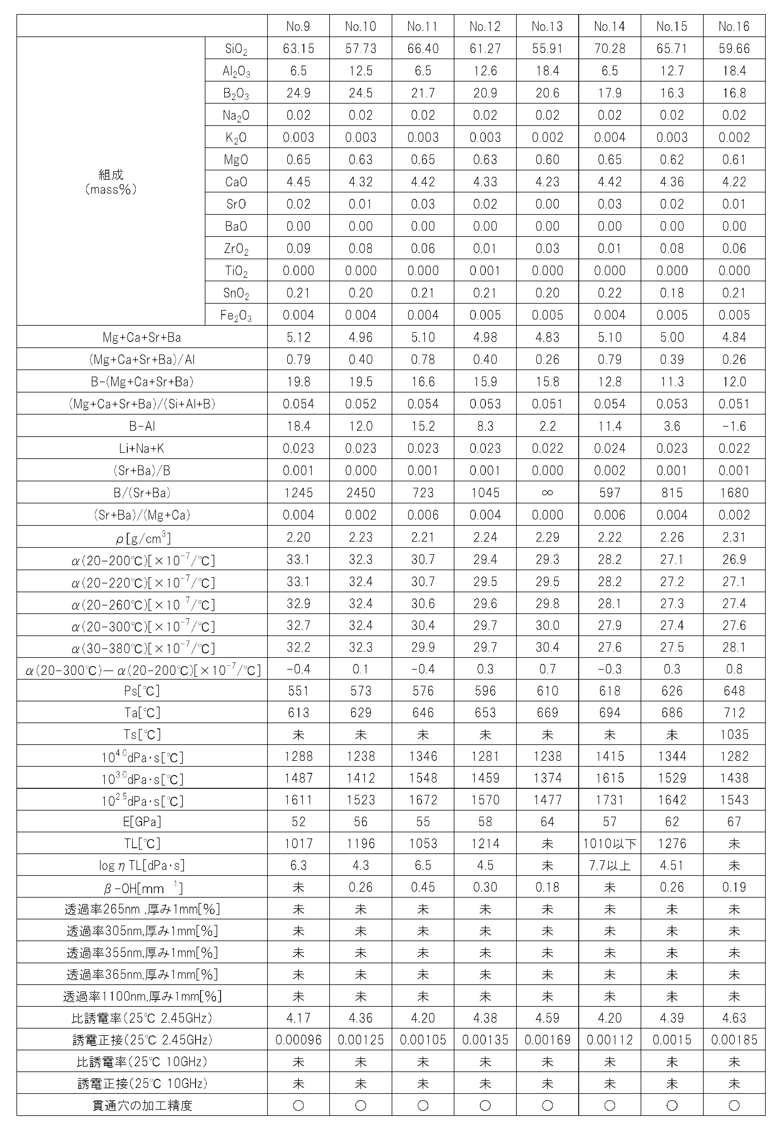


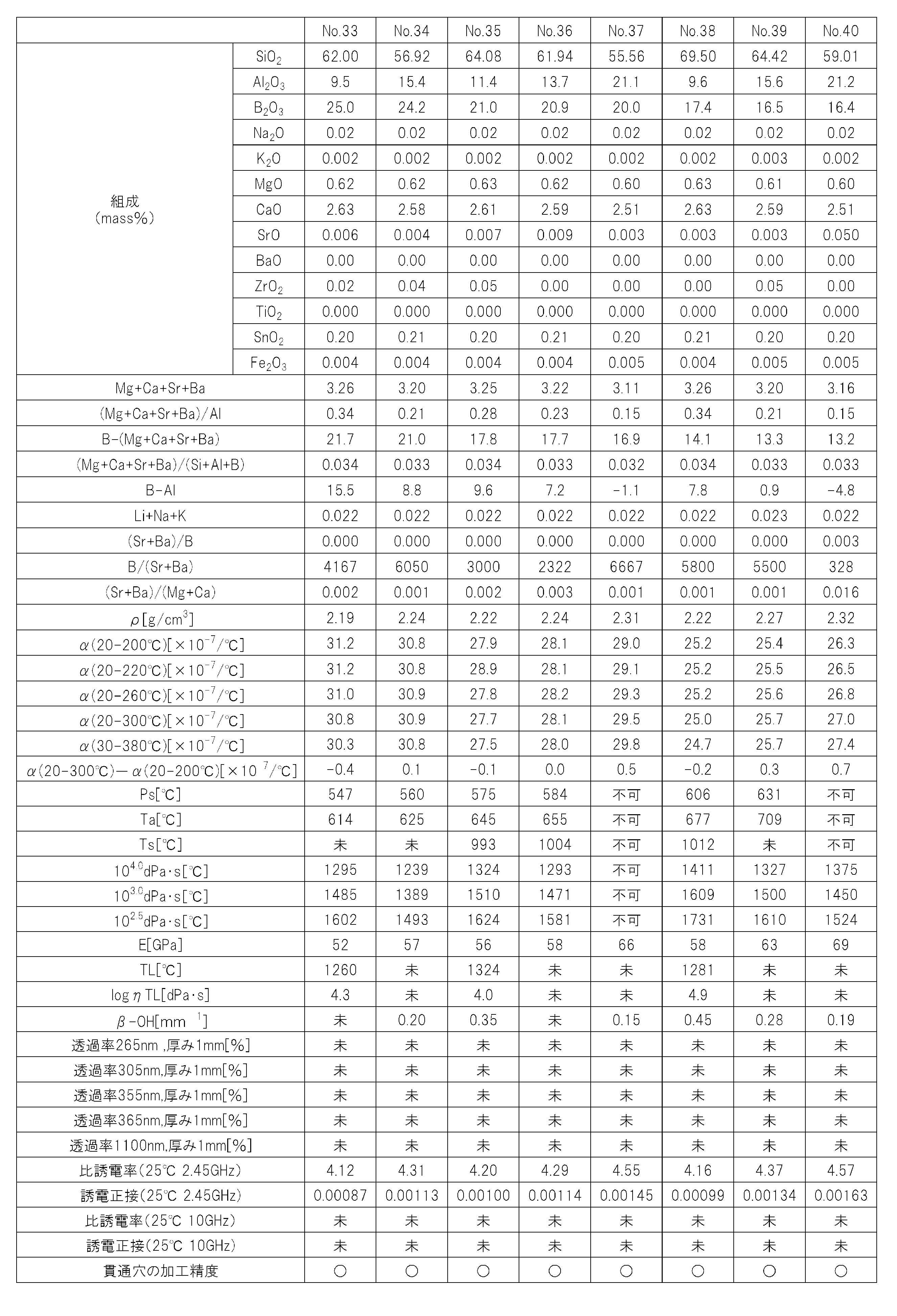
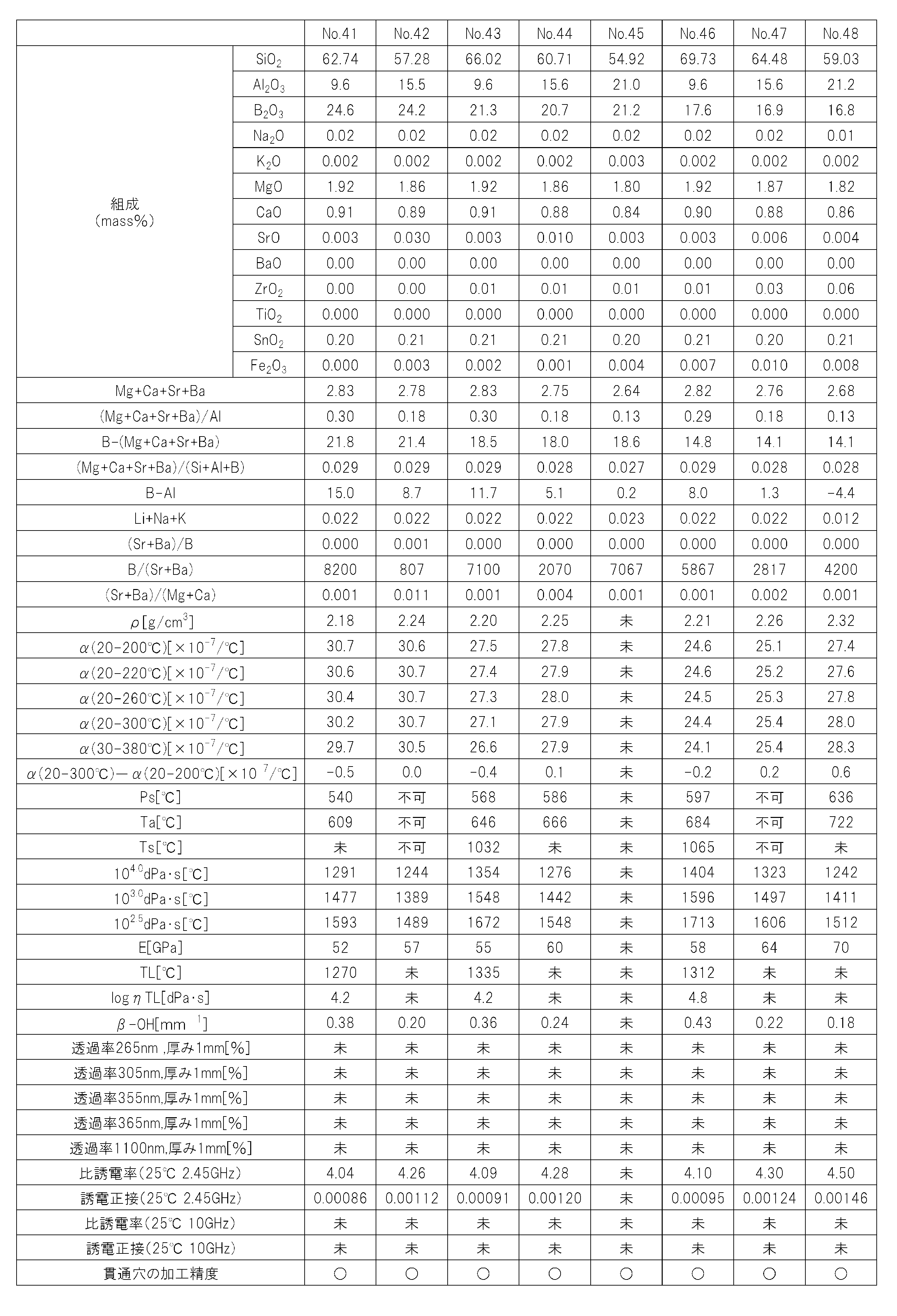
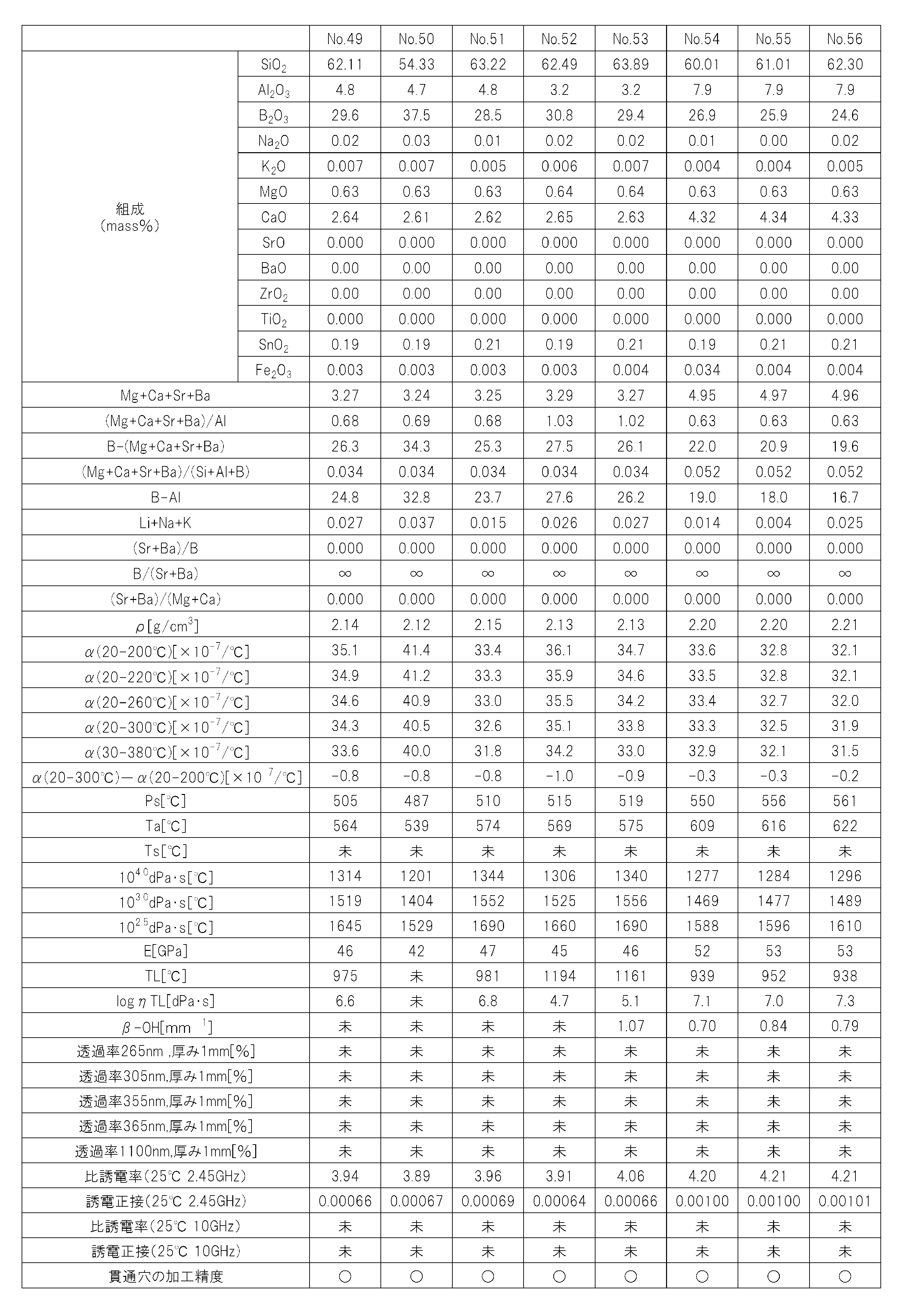
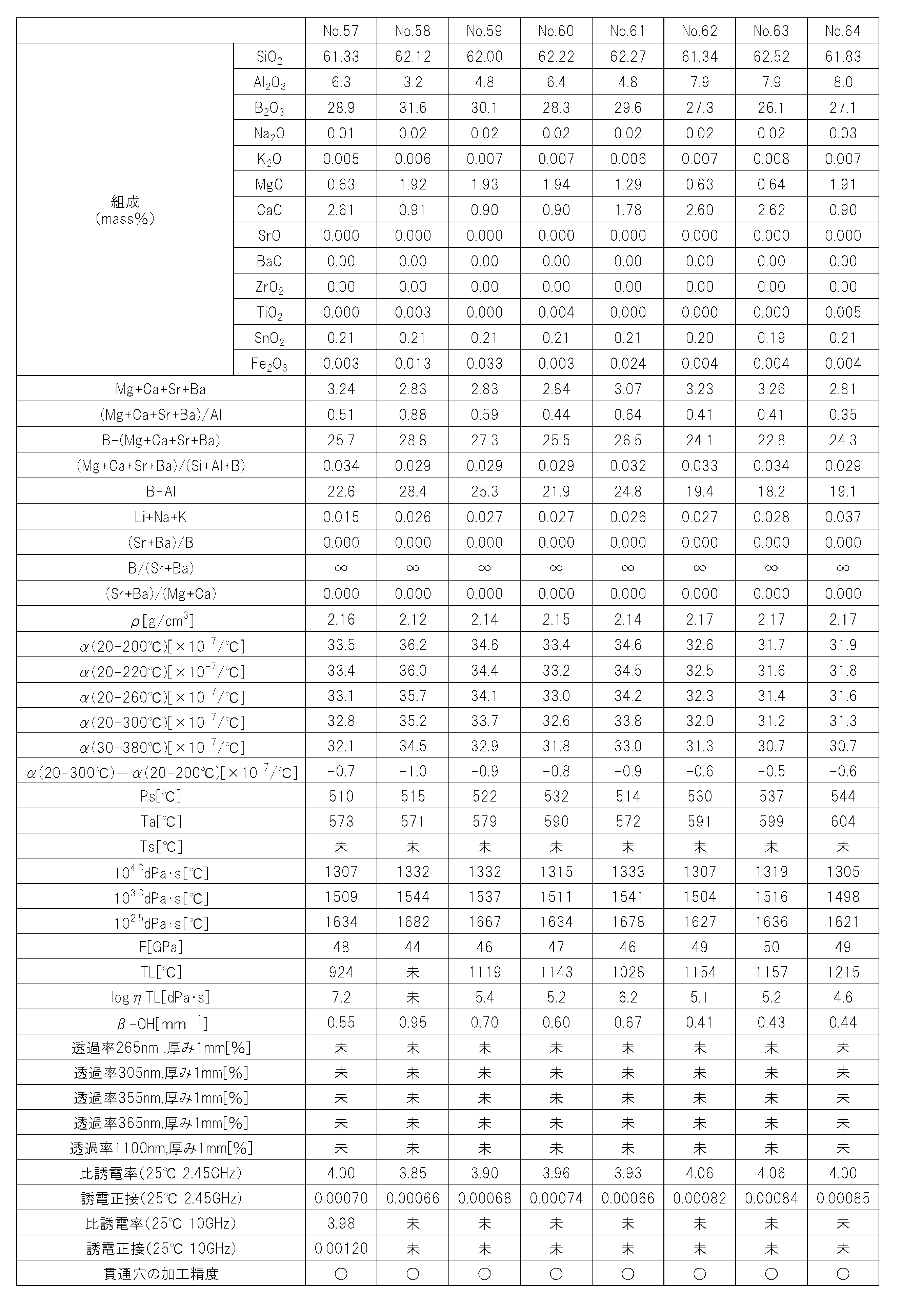
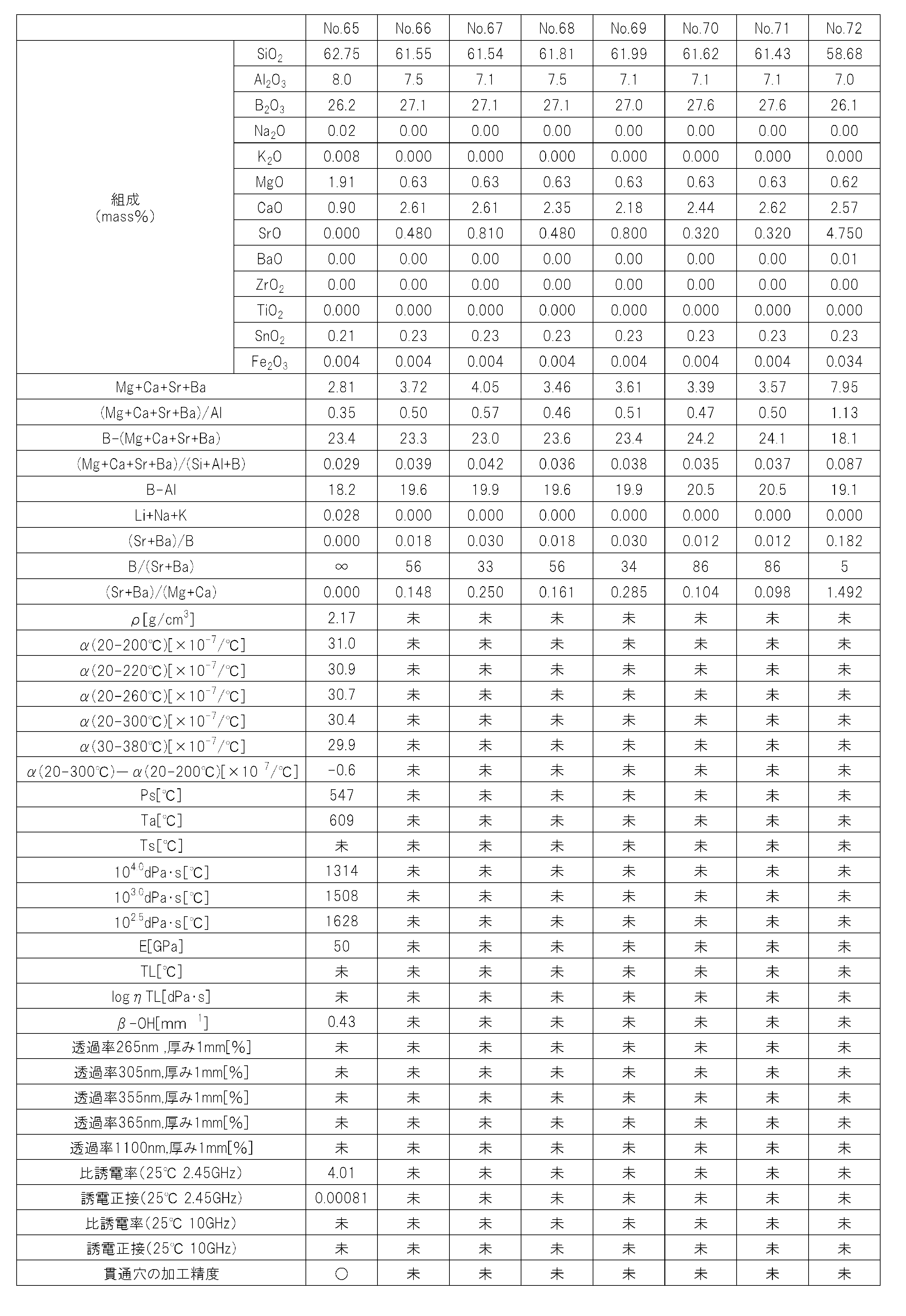
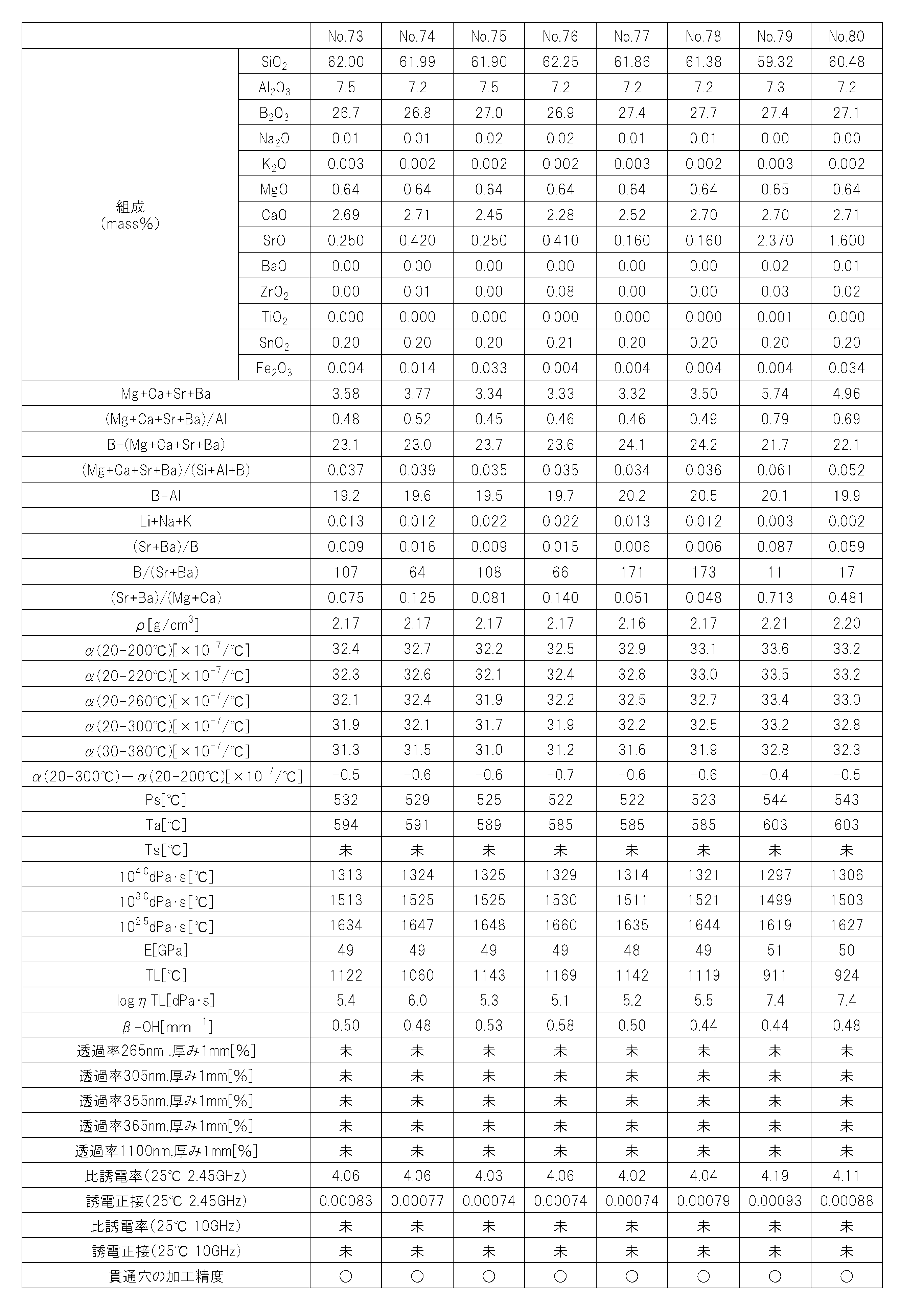
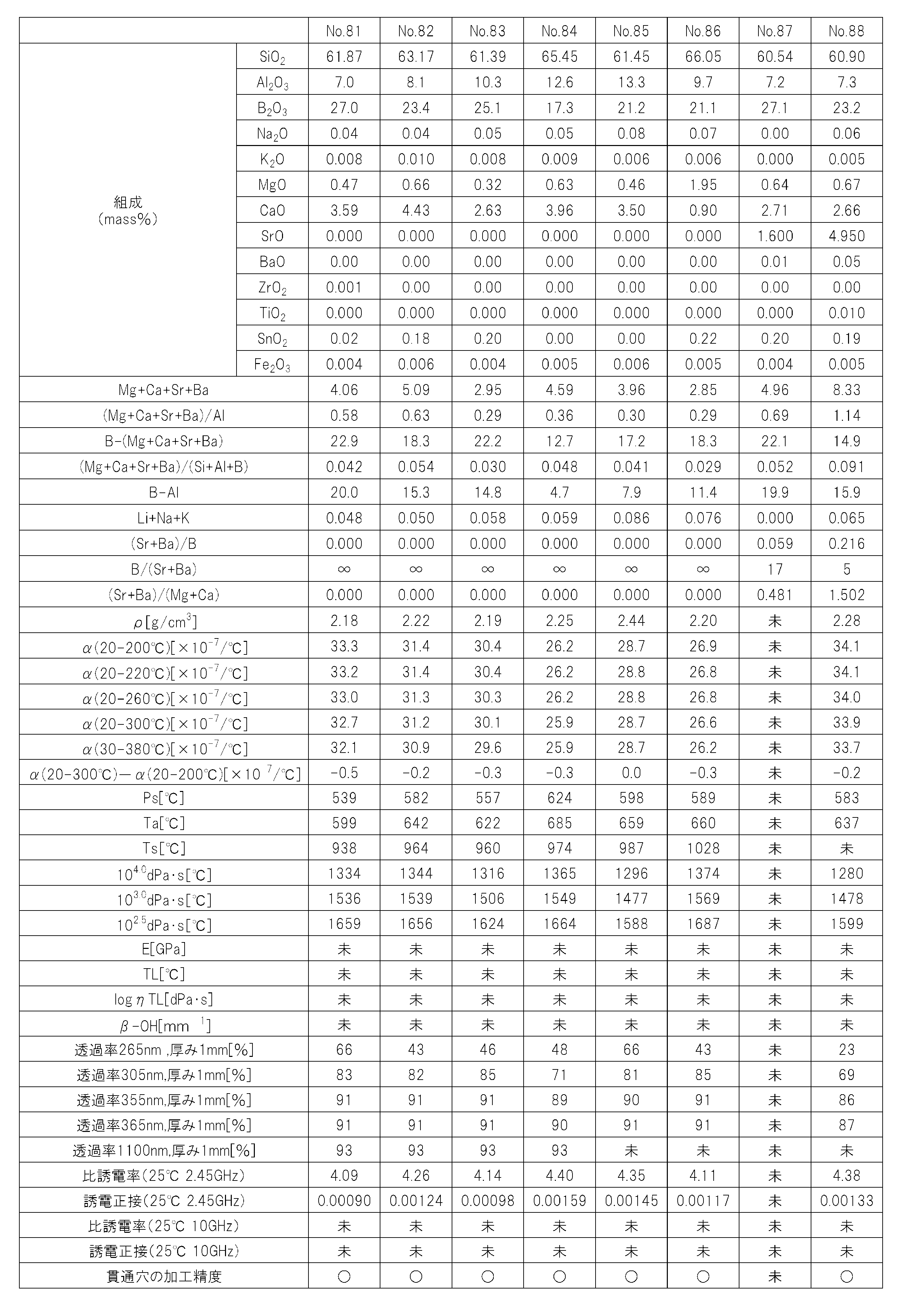


次のようにして、試料No.1~104を作製した。まず表中のガラス組成になるように調合したガラス原料を白金坩堝に入れ、1600℃で24時間溶融した後、カーボン板上に流し出して平形板状に成形した。次に、得られた各試料について、密度ρ、熱膨張係数α、歪点Ps、徐冷点Ta、軟化点Ts、104.0dPa・sにおける温度、103.0dPa・sにおける温度、102.5dPa・sにおける温度、ヤング率E、液相温度TL、液相粘度logηTL、25℃、周波数2.45GHzにおける比誘電率、25℃、周波数2.45GHzにおける誘電正接、25℃、周波数10GHzにおける比誘電率、25℃、周波数10GHzにおける誘電正接、厚み1.0mm換算の外部透過率、及び貫通孔の加工精度を評価した。なお、本実施例では、清澄剤としてSnO2を使用したが、SnO2以外の清澄剤を使用してもよい。また溶融条件やガラスバッチの調整により泡切れが良好であれば、清澄剤を添加しなくてもよい。
密度ρは、周知のアルキメデス法で測定した値である。
熱膨張係数αは、ディラトメーターで測定した値であり、20~200℃、20~220℃、20~260℃、20~300℃及び30~380℃の温度範囲における平均値である。
歪点Ps、徐冷点Ta及び軟化点Tsは、ASTM C336、C338の方法に基づいて測定した値である。
104.0dPa・sにおける温度、103.0dPa・sにおける温度及び102.5dPa・sにおける温度は、白金球引き上げ法で測定した値である。
ヤング率Eは、共振法で測定した値である。ヤング率が大きい程、比ヤング率(ヤング率/密度)が大きくなり易く、平板形状の場合、自重によるガラスの撓みが小さくなる。
液相温度TLは、標準篩30メッシュ(500μm)を通過し、50メッシュ(300μm)に残るガラス粉末を白金ボートに入れ、温度勾配炉中に24時間保持して、結晶の析出する温度を測定した値である。
液相粘度logηTLは、液相温度TLにおけるガラスの粘度を白金球引き上げ法で測定した値である。
25℃、周波数2.45GHzにおける比誘電率、誘電正接及び25℃、周波数10GHzにおける比誘電率、誘電正接は、周知の空洞共振器法で測定した値を指す。
波長265nm、305nm、355nm、365nm及び1100nmにおける厚み1.0mm換算の外部透過率は、両面を光学研磨面(鏡面)に研磨したものを測定試料として、市販の分光光度計(例えば、日本分光社製V―670)で測定した値を指す。
貫通孔の加工精度は、各試料の加工条件を同一にして、貫通孔を形成した際に、内径の最大値と最小値の差が50μm未満であった場合を「○」、内径の最大値と最小値の差が50μm以上であった場合を「×」として評価したものである。
表3に記載の試料No.19のガラス組成になるガラスバッチを試験溶融炉で溶融して、溶融ガラスを得た後、オーバーフローダウンドロー法で板厚0.7mmのガラス板を成形した。なお、ガラス板の成形に際し、引っ張りローラーの速度、冷却ローラーの速度、加熱装置の温度分布、溶融ガラスの温度、溶融ガラスの流量、板引き速度、攪拌スターラーの回転数等を適宜調整することで、ガラス板の熱収縮率、全体板厚偏差及び反りを調節した。次に、得られたガラス板を切断して、外径12インチ(304.8mm)の円板状のガラス板を得た。円板状のガラス板の反り量は100μm以下、全体板厚偏差は5μmであった。なお、「反り量」と「全体板厚偏差」は、コベルコ科研社製のBow/Warp測定装置 SBW-331ML/dにより測定した値である。次に、得られたガラス板の表面の算術平均粗さRaを、原子間力顕微鏡(AFM)で測定したところ、0.2nmであった。
表3に記載の試料No.19、表9の試料No.72のガラス組成になるガラスバッチを試験溶融炉で溶融して、溶融ガラスを得た後、オーバーフローダウンドロー法で板厚0.3mmのガラス板をそれぞれ成形した。次に、得られたガラス板を切断して、300mm×400mmの矩形状のガラス板を得た。次に、矩形状のガラス板に複数の貫通孔を形成した。貫通孔は、市販のピコ秒レーザーをガラス板の表面に照射して、改質層を形成した後、その改質層をエッチングで除去することにより作製した。表3に記載の試料No.19、表12の試料No.91に係る貫通孔の内径をそれぞれ測定したところ、何れも最大値が85μm、最小値が62μm、内径の最大値と最小値の差が23μmであった。また貫通孔から伸長した表面方向のクラックの最大長さは何れも2μmであった。
次に、表3に記載の試料No.19、表9の試料No.72に係るガラス板について、それぞれ高周波デバイスを作製した。まずガラス板の貫通孔に対して、セミアディティブ法により、導体回路層を形成 した。具体的には、スパッタ法によるシード金属層の作製、無電解めっき法による金属層の形成、レジストパターンの形成、配線のための銅めっきの形成を順次行い、導体回路層を形成した。
続いて、ガラス板の両表面上にキャパシタ、コイル等を設けた後、絶縁樹脂層を形成し、ビアホールを作製した。その後、デスミア処理、無電解銅めっき処理を行い、更にドライフィルムレジスト層を形成した。フォトリソグラフィーでレジストパターンを形成した後、電解銅めっき法で導体回路層を形成した。その後、多層回路の形成を繰り返して、ビルドアップ多層回路をガラス板(ガラスコア)の両表面に形成した。
更に、多層回路の最外層に対して、ソルダーレジスト層を形成し、フォトリソグラフィーで外部接続端子部を露出させて、めっきをした後、はんだボールを形成した。はんだボールを設ける工程は、一連の工程で熱処理温度が最も高く、約320℃であった。最後に、はんだボールを形成したガラス板をダイシング加工し、高周波デバイスを得た。
表3に記載の試料No.19、表9の試料No.72のガラス組成になるガラスバッチを試験溶融炉で溶融して、溶融ガラスを得た後、フロート法で板厚5.1mmのガラス板を成形した。次に、得られたガラス板を切断して、350mm×450mmの矩形状のガラス板を得た。このガラス板を5.0mmの厚さになるまで研磨加工した。研磨加工後のガラスの算術平均粗さRaを、触針式表面粗さ計で測定したところ、500nmであった。次に、矩形状のガラス板に複数の貫通孔を形成した。貫通孔は、市販のピコ秒レーザーをガラス板の表面に照射して、改質層を形成した後、その改質層をエッチングで除去することにより作製した。
次に、表3に記載の試料No.19、表9の試料No.72に係るガラス板について、それぞれ高周波デバイスを作製した。まずガラス板の貫通孔に対して、セミアディティブ法により、導体回路層を形成した。具体的には、スパッタ法によるシード金属層の作製、無電解めっき法による金属層の形成、レジストパターンの形成、配線のための銅めっきの形成を順次行い、導体回路層を形成した。
続いて、ガラス板の両表面上にキャパシタ、コイル等を設けた後、絶縁樹脂層を形成し、ビアホールを作製した。その後、デスミア処理、無電解銅めっき処理を行い、更にドライフィルムレジスト層を形成した。フォトリソグラフィーでレジストパターンを形成した後、電解銅めっき法で導体回路層を形成した。その後、多層回路の形成を繰り返して、ビルドアップ多層回路をガラス板(ガラスコア)の両表面に形成した。本プロセスにおいて回路層の剥離は発生しなかった。
更に、多層回路の最外層に対して、ソルダーレジスト層を形成し、フォトリソグラフィーで外部接続端子部を露出させて、めっきをした後、はんだボールを形成した。はんだボールを設ける工程は、一連の工程で熱処理温度が最も高く、約320℃であった。最後に、はんだボールを形成したガラス板をダイシング加工し、高周波デバイスを得た。
本発明のガラス板は、高周波デバイス用途に好適であるが、それ以外にも、低誘電特性が求められるプリント配線板用基板、ガラスアンテナ用基板、マイクロLED用基板、ガラスインターポーザー用基板としても好適である。また、本発明のガラス板は、デュプレクサー等の誘電体フィルターの共振器を構成する部材としても好適である。
Claims (17)
- ガラス組成として、質量%で、SiO2 50~72%、Al2O3 0~22%、B2O3 15~38%、Li2O+Na2O+K2O 0~3%、MgO+CaO+SrO+BaO 0~12%を含有し、25℃、周波数10GHzにおける比誘電率が5以下であることを特徴とするガラス板。
- ガラス組成として、質量%で、SiO2 50~72%、Al2O3 0~22%、B2O3 15~38%、Li2O+Na2O+K2O 0~3%、MgO+CaO+SrO+BaO 0~12%を含有し、25℃、周波数2.45GHzにおける比誘電率が5以下であることを特徴とするガラス板。
- ガラス組成として、質量%で、SiO2 50~72%、Al2O3 0~22%、B2O3 15~38%、Li2O+Na2O+K2O 0~3%、MgO+CaO+SrO+BaO 0~12%を含有することを特徴とするガラス板。
- 質量比(MgO+CaO+SrO+BaO)/(SiO2+Al2O3+B2O3)が0.001~0.4であることを特徴とする請求項1~3の何れか一項に記載のガラス板。
- 板厚方向に複数の貫通孔が形成されていることを特徴とする請求項1~4の何れか一項に記載のガラス板。
- 貫通孔の平均内径が300μm以下であることを特徴とする請求項5に記載のガラス板。
- 貫通孔の内径の最大値と最小値の差が50μm以下であることを特徴とする請求項5又は6に記載のガラス板。
- 貫通孔から伸張した表面方向のクラックの最大長さが100μm以下であることを特徴とする請求項5~7の何れかに記載のガラス板。
- 25℃、周波数10GHzにおける誘電正接が0.01以下であることを特徴とする請求項1~8の何れかに記載のガラス板。
- ヤング率が40GPa以上であることを特徴とする請求項1~9の何れかに記載のガラス板。
- 5℃/分の速度で昇温し、500℃で1時間保持し、5℃/分の速度で降温した時の熱収縮率が30ppm以下であることを特徴とする請求項1~10の何れかに記載のガラス板。
- 30~380℃の温度範囲における熱膨張係数が20×10-7~50×10-7/℃であることを特徴とする請求項1~11の何れかに記載のガラス板。
- 20~300℃の温度範囲における熱膨張係数と20~200℃の温度範囲における熱膨張係数との差が1.0×10⁻⁷/℃以下であることを特徴とする請求項1~12の何れかに記載のガラス板。
- 波長355nmにおける厚み1.0mm換算の外部透過率が80%以上であることを特徴とする請求項1~13の何れかに記載のガラス板。
- 波長265nmにおける厚み1.0mm換算の外部透過率が15%以上であることを特徴とする請求項1~14の何れかに記載のガラス板。
- 液相粘度が104.0dPa・s以上であることを特徴とする請求項1~15の何れかに記載のガラス板。
- オーバーフローダウンドロー法で成形されてなることを特徴とする請求項1~16の何れかに記載のガラス板。
Priority Applications (4)
| Application Number | Priority Date | Filing Date | Title |
|---|---|---|---|
| US17/434,185 US20220169555A1 (en) | 2019-03-08 | 2020-02-26 | Glass sheet |
| JP2021504900A JP7777278B2 (ja) | 2019-03-08 | 2020-02-26 | ガラス板 |
| CN202080019384.5A CN113544102A (zh) | 2019-03-08 | 2020-02-26 | 玻璃板 |
| CN202410351117.8A CN118221348A (zh) | 2019-03-08 | 2020-02-26 | 玻璃板 |
Applications Claiming Priority (8)
| Application Number | Priority Date | Filing Date | Title |
|---|---|---|---|
| JP2019-042163 | 2019-03-08 | ||
| JP2019042163 | 2019-03-08 | ||
| JP2019-091144 | 2019-05-14 | ||
| JP2019091144 | 2019-05-14 | ||
| JP2019-122940 | 2019-07-01 | ||
| JP2019122940 | 2019-07-01 | ||
| JP2019162870 | 2019-09-06 | ||
| JP2019-162870 | 2019-09-06 |
Publications (1)
| Publication Number | Publication Date |
|---|---|
| WO2020184175A1 true WO2020184175A1 (ja) | 2020-09-17 |
Family
ID=72426604
Family Applications (1)
| Application Number | Title | Priority Date | Filing Date |
|---|---|---|---|
| PCT/JP2020/007596 Ceased WO2020184175A1 (ja) | 2019-03-08 | 2020-02-26 | ガラス板 |
Country Status (4)
| Country | Link |
|---|---|
| US (1) | US20220169555A1 (ja) |
| JP (1) | JP7777278B2 (ja) |
| CN (2) | CN118221348A (ja) |
| WO (1) | WO2020184175A1 (ja) |
Cited By (3)
| Publication number | Priority date | Publication date | Assignee | Title |
|---|---|---|---|---|
| WO2022102598A1 (ja) * | 2020-11-16 | 2022-05-19 | 日本電気硝子株式会社 | ガラス基板 |
| WO2023026770A1 (ja) * | 2021-08-24 | 2023-03-02 | 日本電気硝子株式会社 | 支持ガラス基板、積層体、積層体の製造方法及び半導体パッケージの製造方法 |
| WO2023162788A1 (ja) * | 2022-02-24 | 2023-08-31 | Agc株式会社 | 無アルカリガラスおよびガラス板 |
Families Citing this family (1)
| Publication number | Priority date | Publication date | Assignee | Title |
|---|---|---|---|---|
| JP2024070324A (ja) * | 2022-11-11 | 2024-05-23 | 日本電気硝子株式会社 | 配線基板補強用ガラス基板 |
Citations (2)
| Publication number | Priority date | Publication date | Assignee | Title |
|---|---|---|---|---|
| WO2018051793A1 (ja) * | 2016-09-13 | 2018-03-22 | 旭硝子株式会社 | 高周波デバイス用ガラス基板と高周波デバイス用回路基板 |
| JP2018531205A (ja) * | 2015-10-09 | 2018-10-25 | コーニング インコーポレイテッド | ビアを有するガラス系基板およびそれを形成するプロセス |
Family Cites Families (12)
| Publication number | Priority date | Publication date | Assignee | Title |
|---|---|---|---|---|
| JP2002080240A (ja) * | 2000-09-08 | 2002-03-19 | Asahi Glass Co Ltd | 低誘電率無アルカリガラス |
| JP2003026446A (ja) * | 2001-07-16 | 2003-01-29 | Asahi Glass Co Ltd | 電子回路基板用組成物および電子回路基板 |
| US7678721B2 (en) * | 2006-10-26 | 2010-03-16 | Agy Holding Corp. | Low dielectric glass fiber |
| CN101012105B (zh) * | 2006-12-21 | 2010-05-19 | 泰山玻璃纤维股份有限公司 | 一种低介电常数玻璃纤维 |
| JP2010030849A (ja) * | 2008-07-30 | 2010-02-12 | Ohara Inc | ガラス |
| KR101446971B1 (ko) * | 2009-03-19 | 2014-10-06 | 니폰 덴키 가라스 가부시키가이샤 | 무알칼리 유리 |
| JP2011063464A (ja) * | 2009-09-16 | 2011-03-31 | Nippon Electric Glass Co Ltd | プラズマディスプレイ用ガラス板 |
| CN113060935A (zh) * | 2013-08-15 | 2021-07-02 | 康宁股份有限公司 | 掺杂有碱金属和不含碱金属的硼铝硅酸盐玻璃 |
| CN103482876B (zh) * | 2013-09-18 | 2016-01-20 | 重庆理工大学 | 一种用于印刷电路板的玻璃纤维及其制备方法 |
| CN106414358B (zh) * | 2013-11-20 | 2021-08-13 | 康宁股份有限公司 | 耐划痕的硼铝硅酸盐玻璃 |
| JP6691315B2 (ja) * | 2014-04-03 | 2020-04-28 | 日本電気硝子株式会社 | ガラス |
| JPWO2016088778A1 (ja) * | 2014-12-02 | 2017-09-14 | 旭硝子株式会社 | ガラス板およびそれを用いた加熱器 |
-
2020
- 2020-02-26 US US17/434,185 patent/US20220169555A1/en not_active Abandoned
- 2020-02-26 CN CN202410351117.8A patent/CN118221348A/zh active Pending
- 2020-02-26 WO PCT/JP2020/007596 patent/WO2020184175A1/ja not_active Ceased
- 2020-02-26 CN CN202080019384.5A patent/CN113544102A/zh active Pending
- 2020-02-26 JP JP2021504900A patent/JP7777278B2/ja active Active
Patent Citations (2)
| Publication number | Priority date | Publication date | Assignee | Title |
|---|---|---|---|---|
| JP2018531205A (ja) * | 2015-10-09 | 2018-10-25 | コーニング インコーポレイテッド | ビアを有するガラス系基板およびそれを形成するプロセス |
| WO2018051793A1 (ja) * | 2016-09-13 | 2018-03-22 | 旭硝子株式会社 | 高周波デバイス用ガラス基板と高周波デバイス用回路基板 |
Cited By (5)
| Publication number | Priority date | Publication date | Assignee | Title |
|---|---|---|---|---|
| WO2022102598A1 (ja) * | 2020-11-16 | 2022-05-19 | 日本電気硝子株式会社 | ガラス基板 |
| JPWO2022102598A1 (ja) * | 2020-11-16 | 2022-05-19 | ||
| JP7787500B2 (ja) | 2020-11-16 | 2025-12-17 | 日本電気硝子株式会社 | ガラス基板 |
| WO2023026770A1 (ja) * | 2021-08-24 | 2023-03-02 | 日本電気硝子株式会社 | 支持ガラス基板、積層体、積層体の製造方法及び半導体パッケージの製造方法 |
| WO2023162788A1 (ja) * | 2022-02-24 | 2023-08-31 | Agc株式会社 | 無アルカリガラスおよびガラス板 |
Also Published As
| Publication number | Publication date |
|---|---|
| CN113544102A (zh) | 2021-10-22 |
| CN118221348A (zh) | 2024-06-21 |
| US20220169555A1 (en) | 2022-06-02 |
| JP7777278B2 (ja) | 2025-11-28 |
| JPWO2020184175A1 (ja) | 2020-09-17 |
Similar Documents
| Publication | Publication Date | Title |
|---|---|---|
| JP7777278B2 (ja) | ガラス板 | |
| JP2022159373A (ja) | 高周波デバイス用ガラス基板と高周波デバイス用回路基板 | |
| KR102809238B1 (ko) | 전자 장치용 저 유전 손실 유리 | |
| KR102436789B1 (ko) | 적층체, 반도체 패키지 제조 방법, 반도체 패키지 및 전자기기 | |
| CN113396132A (zh) | 微晶玻璃、化学强化玻璃和半导体支撑基板 | |
| KR102402822B1 (ko) | 지지 유리 기판 및 이것을 사용한 적층체 | |
| CN113661148A (zh) | 无碱玻璃和玻璃板 | |
| US20240360027A1 (en) | Support glass substrate, multi-layer body, method for producing multi-layer body, and method for producing semiconductor package | |
| JP2025100891A (ja) | 積層板 | |
| KR102509782B1 (ko) | 지지 유리 기판 및 이것을 사용한 적층체 | |
| CN116096683B (zh) | 玻璃及使用了该玻璃的介电特性的测定方法 | |
| JP7846450B2 (ja) | ガラスフィルム及びこれを用いたガラスロール | |
| US20250187972A1 (en) | Phase separated glasses | |
| US20220396519A1 (en) | Glass compositions having improved mechanical durability and low characteristic temperatures | |
| JP2023031216A (ja) | 支持ガラス基板、積層体、積層体の製造方法及び半導体パッケージの製造方法 | |
| US20250236553A1 (en) | Method of improving dielectric performance of alumino-borosilicate glass | |
| WO2025239392A1 (ja) | 支持ガラス基板、積層体、積層体の製造方法、半導体パッケージの製造方法及びガラス基板 |
Legal Events
| Date | Code | Title | Description |
|---|---|---|---|
| 121 | Ep: the epo has been informed by wipo that ep was designated in this application |
Ref document number: 20770141 Country of ref document: EP Kind code of ref document: A1 |
|
| ENP | Entry into the national phase |
Ref document number: 2021504900 Country of ref document: JP Kind code of ref document: A |
|
| NENP | Non-entry into the national phase |
Ref country code: DE |
|
| 122 | Ep: pct application non-entry in european phase |
Ref document number: 20770141 Country of ref document: EP Kind code of ref document: A1 |