WO2020184016A1 - 撮像素子、撮像素子の製造方法及び撮像装置 - Google Patents
撮像素子、撮像素子の製造方法及び撮像装置 Download PDFInfo
- Publication number
- WO2020184016A1 WO2020184016A1 PCT/JP2020/004774 JP2020004774W WO2020184016A1 WO 2020184016 A1 WO2020184016 A1 WO 2020184016A1 JP 2020004774 W JP2020004774 W JP 2020004774W WO 2020184016 A1 WO2020184016 A1 WO 2020184016A1
- Authority
- WO
- WIPO (PCT)
- Prior art keywords
- electrode
- photoelectric conversion
- electron blocking
- blocking layer
- conversion layer
- Prior art date
Links
- 238000003384 imaging method Methods 0.000 title claims abstract description 9
- 238000004519 manufacturing process Methods 0.000 title claims description 16
- 238000006243 chemical reaction Methods 0.000 claims abstract description 145
- 230000000903 blocking effect Effects 0.000 claims abstract description 109
- OKTJSMMVPCPJKN-UHFFFAOYSA-N Carbon Chemical compound [C] OKTJSMMVPCPJKN-UHFFFAOYSA-N 0.000 claims abstract description 27
- 229910052799 carbon Inorganic materials 0.000 claims abstract description 27
- WGLPBDUCMAPZCE-UHFFFAOYSA-N Trioxochromium Chemical compound O=[Cr](=O)=O WGLPBDUCMAPZCE-UHFFFAOYSA-N 0.000 claims abstract description 23
- 229910000423 chromium oxide Inorganic materials 0.000 claims abstract description 21
- 239000000463 material Substances 0.000 claims description 59
- 238000000034 method Methods 0.000 claims description 40
- 238000003860 storage Methods 0.000 claims description 21
- 238000001514 detection method Methods 0.000 claims description 10
- 239000011368 organic material Substances 0.000 claims description 9
- 238000010521 absorption reaction Methods 0.000 claims description 8
- 150000002902 organometallic compounds Chemical class 0.000 claims description 5
- 238000000354 decomposition reaction Methods 0.000 claims description 4
- 238000012546 transfer Methods 0.000 claims description 3
- 239000010410 layer Substances 0.000 description 212
- 239000004065 semiconductor Substances 0.000 description 44
- 239000000758 substrate Substances 0.000 description 36
- 239000012535 impurity Substances 0.000 description 32
- 150000002894 organic compounds Chemical class 0.000 description 22
- 230000003321 amplification Effects 0.000 description 21
- 238000003199 nucleic acid amplification method Methods 0.000 description 21
- 239000010408 film Substances 0.000 description 18
- 239000000243 solution Substances 0.000 description 14
- 239000010409 thin film Substances 0.000 description 13
- 230000006870 function Effects 0.000 description 11
- 239000011651 chromium Substances 0.000 description 10
- 239000011248 coating agent Substances 0.000 description 10
- 229910052751 metal Inorganic materials 0.000 description 10
- 239000002184 metal Substances 0.000 description 10
- 239000000370 acceptor Substances 0.000 description 9
- -1 hydrazone compounds Chemical class 0.000 description 9
- XLOMVQKBTHCTTD-UHFFFAOYSA-N Zinc monoxide Chemical compound [Zn]=O XLOMVQKBTHCTTD-UHFFFAOYSA-N 0.000 description 8
- 238000000576 coating method Methods 0.000 description 8
- 150000001875 compounds Chemical class 0.000 description 8
- 238000012545 processing Methods 0.000 description 8
- 238000000231 atomic layer deposition Methods 0.000 description 6
- 238000005229 chemical vapour deposition Methods 0.000 description 6
- 229920001940 conductive polymer Polymers 0.000 description 6
- RAXXELZNTBOGNW-UHFFFAOYSA-N imidazole Natural products C1=CNC=N1 RAXXELZNTBOGNW-UHFFFAOYSA-N 0.000 description 6
- 239000011229 interlayer Substances 0.000 description 6
- 229910021420 polycrystalline silicon Inorganic materials 0.000 description 6
- 229920005591 polysilicon Polymers 0.000 description 6
- 230000000052 comparative effect Effects 0.000 description 5
- 230000000875 corresponding effect Effects 0.000 description 5
- 229910010272 inorganic material Inorganic materials 0.000 description 5
- 239000011147 inorganic material Substances 0.000 description 5
- 229910044991 metal oxide Inorganic materials 0.000 description 5
- 150000004706 metal oxides Chemical class 0.000 description 5
- 239000000126 substance Substances 0.000 description 5
- 238000001035 drying Methods 0.000 description 4
- 230000006872 improvement Effects 0.000 description 4
- 230000010354 integration Effects 0.000 description 4
- 150000004767 nitrides Chemical class 0.000 description 4
- 238000000926 separation method Methods 0.000 description 4
- 238000007740 vapor deposition Methods 0.000 description 4
- 239000012808 vapor phase Substances 0.000 description 4
- 239000011787 zinc oxide Substances 0.000 description 4
- RYGMFSIKBFXOCR-UHFFFAOYSA-N Copper Chemical compound [Cu] RYGMFSIKBFXOCR-UHFFFAOYSA-N 0.000 description 3
- RWRDLPDLKQPQOW-UHFFFAOYSA-N Pyrrolidine Chemical compound C1CCNC1 RWRDLPDLKQPQOW-UHFFFAOYSA-N 0.000 description 3
- XUIMIQQOPSSXEZ-UHFFFAOYSA-N Silicon Chemical compound [Si] XUIMIQQOPSSXEZ-UHFFFAOYSA-N 0.000 description 3
- 238000004833 X-ray photoelectron spectroscopy Methods 0.000 description 3
- 125000004429 atom Chemical group 0.000 description 3
- 229910052802 copper Inorganic materials 0.000 description 3
- 239000010949 copper Substances 0.000 description 3
- 238000002425 crystallisation Methods 0.000 description 3
- 230000008025 crystallization Effects 0.000 description 3
- 238000010586 diagram Methods 0.000 description 3
- 230000031700 light absorption Effects 0.000 description 3
- 150000002739 metals Chemical class 0.000 description 3
- 230000002093 peripheral effect Effects 0.000 description 3
- 229910052710 silicon Inorganic materials 0.000 description 3
- 239000010703 silicon Substances 0.000 description 3
- 238000002834 transmittance Methods 0.000 description 3
- MAGFQRLKWCCTQJ-UHFFFAOYSA-N 4-ethenylbenzenesulfonic acid Chemical compound OS(=O)(=O)C1=CC=C(C=C)C=C1 MAGFQRLKWCCTQJ-UHFFFAOYSA-N 0.000 description 2
- KDCGOANMDULRCW-UHFFFAOYSA-N 7H-purine Chemical compound N1=CNC2=NC=NC2=C1 KDCGOANMDULRCW-UHFFFAOYSA-N 0.000 description 2
- UJOBWOGCFQCDNV-UHFFFAOYSA-N 9H-carbazole Chemical compound C1=CC=C2C3=CC=CC=C3NC2=C1 UJOBWOGCFQCDNV-UHFFFAOYSA-N 0.000 description 2
- XMWRBQBLMFGWIX-UHFFFAOYSA-N C60 fullerene Chemical compound C12=C3C(C4=C56)=C7C8=C5C5=C9C%10=C6C6=C4C1=C1C4=C6C6=C%10C%10=C9C9=C%11C5=C8C5=C8C7=C3C3=C7C2=C1C1=C2C4=C6C4=C%10C6=C9C9=C%11C5=C5C8=C3C3=C7C1=C1C2=C4C6=C2C9=C5C3=C12 XMWRBQBLMFGWIX-UHFFFAOYSA-N 0.000 description 2
- VYZAMTAEIAYCRO-UHFFFAOYSA-N Chromium Chemical compound [Cr] VYZAMTAEIAYCRO-UHFFFAOYSA-N 0.000 description 2
- PCNDJXKNXGMECE-UHFFFAOYSA-N Phenazine Natural products C1=CC=CC2=NC3=CC=CC=C3N=C21 PCNDJXKNXGMECE-UHFFFAOYSA-N 0.000 description 2
- 229920001609 Poly(3,4-ethylenedioxythiophene) Polymers 0.000 description 2
- KYQCOXFCLRTKLS-UHFFFAOYSA-N Pyrazine Chemical compound C1=CN=CC=N1 KYQCOXFCLRTKLS-UHFFFAOYSA-N 0.000 description 2
- JUJWROOIHBZHMG-UHFFFAOYSA-N Pyridine Chemical compound C1=CC=NC=C1 JUJWROOIHBZHMG-UHFFFAOYSA-N 0.000 description 2
- SMWDFEZZVXVKRB-UHFFFAOYSA-N Quinoline Chemical compound N1=CC=CC2=CC=CC=C21 SMWDFEZZVXVKRB-UHFFFAOYSA-N 0.000 description 2
- BQCADISMDOOEFD-UHFFFAOYSA-N Silver Chemical compound [Ag] BQCADISMDOOEFD-UHFFFAOYSA-N 0.000 description 2
- 229910006404 SnO 2 Inorganic materials 0.000 description 2
- 229910010413 TiO 2 Inorganic materials 0.000 description 2
- ATJFFYVFTNAWJD-UHFFFAOYSA-N Tin Chemical group [Sn] ATJFFYVFTNAWJD-UHFFFAOYSA-N 0.000 description 2
- RTAQQCXQSZGOHL-UHFFFAOYSA-N Titanium Chemical compound [Ti] RTAQQCXQSZGOHL-UHFFFAOYSA-N 0.000 description 2
- 230000002411 adverse Effects 0.000 description 2
- 229910052782 aluminium Inorganic materials 0.000 description 2
- XAGFODPZIPBFFR-UHFFFAOYSA-N aluminium Chemical compound [Al] XAGFODPZIPBFFR-UHFFFAOYSA-N 0.000 description 2
- 150000001454 anthracenes Chemical class 0.000 description 2
- 150000001601 aromatic carbocyclic compounds Chemical class 0.000 description 2
- 230000004888 barrier function Effects 0.000 description 2
- IOJUPLGTWVMSFF-UHFFFAOYSA-N benzothiazole Chemical compound C1=CC=C2SC=NC2=C1 IOJUPLGTWVMSFF-UHFFFAOYSA-N 0.000 description 2
- 229910052804 chromium Inorganic materials 0.000 description 2
- 230000001276 controlling effect Effects 0.000 description 2
- 150000004696 coordination complex Chemical class 0.000 description 2
- 239000013078 crystal Substances 0.000 description 2
- 230000007547 defect Effects 0.000 description 2
- 230000005684 electric field Effects 0.000 description 2
- 238000010304 firing Methods 0.000 description 2
- 239000011521 glass Substances 0.000 description 2
- 238000002347 injection Methods 0.000 description 2
- 239000007924 injection Substances 0.000 description 2
- AWJUIBRHMBBTKR-UHFFFAOYSA-N isoquinoline Chemical compound C1=NC=CC2=CC=CC=C21 AWJUIBRHMBBTKR-UHFFFAOYSA-N 0.000 description 2
- 238000005259 measurement Methods 0.000 description 2
- 239000012528 membrane Substances 0.000 description 2
- 239000002923 metal particle Substances 0.000 description 2
- 239000000203 mixture Substances 0.000 description 2
- 238000012986 modification Methods 0.000 description 2
- 230000004048 modification Effects 0.000 description 2
- 150000002790 naphthalenes Chemical class 0.000 description 2
- 230000003287 optical effect Effects 0.000 description 2
- 239000003960 organic solvent Substances 0.000 description 2
- 239000002245 particle Substances 0.000 description 2
- 125000002080 perylenyl group Chemical group C1(=CC=C2C=CC=C3C4=CC=CC5=CC=CC(C1=C23)=C45)* 0.000 description 2
- 150000002987 phenanthrenes Chemical class 0.000 description 2
- CLYVDMAATCIVBF-UHFFFAOYSA-N pigment red 224 Chemical compound C=12C3=CC=C(C(OC4=O)=O)C2=C4C=CC=1C1=CC=C2C(=O)OC(=O)C4=CC=C3C1=C42 CLYVDMAATCIVBF-UHFFFAOYSA-N 0.000 description 2
- 238000007747 plating Methods 0.000 description 2
- 229920000412 polyarylene Chemical class 0.000 description 2
- 239000002861 polymer material Substances 0.000 description 2
- 150000003220 pyrenes Chemical class 0.000 description 2
- XSCHRSMBECNVNS-UHFFFAOYSA-N quinoxaline Chemical compound N1=CC=NC2=CC=CC=C21 XSCHRSMBECNVNS-UHFFFAOYSA-N 0.000 description 2
- 239000002994 raw material Substances 0.000 description 2
- 230000035945 sensitivity Effects 0.000 description 2
- 229910052709 silver Inorganic materials 0.000 description 2
- 239000004332 silver Substances 0.000 description 2
- 239000002904 solvent Substances 0.000 description 2
- 238000004544 sputter deposition Methods 0.000 description 2
- 150000003518 tetracenes Chemical class 0.000 description 2
- 229910052719 titanium Inorganic materials 0.000 description 2
- 239000010936 titanium Substances 0.000 description 2
- WFKWXMTUELFFGS-UHFFFAOYSA-N tungsten Chemical compound [W] WFKWXMTUELFFGS-UHFFFAOYSA-N 0.000 description 2
- 229910052721 tungsten Inorganic materials 0.000 description 2
- 239000010937 tungsten Substances 0.000 description 2
- QGKMIGUHVLGJBR-UHFFFAOYSA-M (4z)-1-(3-methylbutyl)-4-[[1-(3-methylbutyl)quinolin-1-ium-4-yl]methylidene]quinoline;iodide Chemical class [I-].C12=CC=CC=C2N(CCC(C)C)C=CC1=CC1=CC=[N+](CCC(C)C)C2=CC=CC=C12 QGKMIGUHVLGJBR-UHFFFAOYSA-M 0.000 description 1
- UWRZIZXBOLBCON-VOTSOKGWSA-N (e)-2-phenylethenamine Chemical class N\C=C\C1=CC=CC=C1 UWRZIZXBOLBCON-VOTSOKGWSA-N 0.000 description 1
- POILWHVDKZOXJZ-ARJAWSKDSA-M (z)-4-oxopent-2-en-2-olate Chemical compound C\C([O-])=C\C(C)=O POILWHVDKZOXJZ-ARJAWSKDSA-M 0.000 description 1
- JYEUMXHLPRZUAT-UHFFFAOYSA-N 1,2,3-triazine Chemical compound C1=CN=NN=C1 JYEUMXHLPRZUAT-UHFFFAOYSA-N 0.000 description 1
- BCMCBBGGLRIHSE-UHFFFAOYSA-N 1,3-benzoxazole Chemical compound C1=CC=C2OC=NC2=C1 BCMCBBGGLRIHSE-UHFFFAOYSA-N 0.000 description 1
- BAXOFTOLAUCFNW-UHFFFAOYSA-N 1H-indazole Chemical compound C1=CC=C2C=NNC2=C1 BAXOFTOLAUCFNW-UHFFFAOYSA-N 0.000 description 1
- XWIYUCRMWCHYJR-UHFFFAOYSA-N 1h-pyrrolo[3,2-b]pyridine Chemical compound C1=CC=C2NC=CC2=N1 XWIYUCRMWCHYJR-UHFFFAOYSA-N 0.000 description 1
- VEPOHXYIFQMVHW-XOZOLZJESA-N 2,3-dihydroxybutanedioic acid (2S,3S)-3,4-dimethyl-2-phenylmorpholine Chemical compound OC(C(O)C(O)=O)C(O)=O.C[C@H]1[C@@H](OCCN1C)c1ccccc1 VEPOHXYIFQMVHW-XOZOLZJESA-N 0.000 description 1
- CBHTTYDJRXOHHL-UHFFFAOYSA-N 2h-triazolo[4,5-c]pyridazine Chemical compound N1=NC=CC2=C1N=NN2 CBHTTYDJRXOHHL-UHFFFAOYSA-N 0.000 description 1
- LCGTWRLJTMHIQZ-UHFFFAOYSA-N 5H-dibenzo[b,f]azepine Chemical compound C1=CC2=CC=CC=C2NC2=CC=CC=C21 LCGTWRLJTMHIQZ-UHFFFAOYSA-N 0.000 description 1
- SIKJAQJRHWYJAI-UHFFFAOYSA-N Indole Chemical class C1=CC=C2NC=CC2=C1 SIKJAQJRHWYJAI-UHFFFAOYSA-N 0.000 description 1
- ZCQWOFVYLHDMMC-UHFFFAOYSA-N Oxazole Chemical compound C1=COC=N1 ZCQWOFVYLHDMMC-UHFFFAOYSA-N 0.000 description 1
- WTKZEGDFNFYCGP-UHFFFAOYSA-N Pyrazole Chemical compound C=1C=NNC=1 WTKZEGDFNFYCGP-UHFFFAOYSA-N 0.000 description 1
- CZPWVGJYEJSRLH-UHFFFAOYSA-N Pyrimidine Chemical compound C1=CN=CN=C1 CZPWVGJYEJSRLH-UHFFFAOYSA-N 0.000 description 1
- KAESVJOAVNADME-UHFFFAOYSA-N Pyrrole Chemical class C=1C=CNC=1 KAESVJOAVNADME-UHFFFAOYSA-N 0.000 description 1
- FZWLAAWBMGSTSO-UHFFFAOYSA-N Thiazole Chemical compound C1=CSC=N1 FZWLAAWBMGSTSO-UHFFFAOYSA-N 0.000 description 1
- DGEZNRSVGBDHLK-UHFFFAOYSA-N [1,10]phenanthroline Chemical compound C1=CN=C2C3=NC=CC=C3C=CC2=C1 DGEZNRSVGBDHLK-UHFFFAOYSA-N 0.000 description 1
- 238000000862 absorption spectrum Methods 0.000 description 1
- 229910021417 amorphous silicon Inorganic materials 0.000 description 1
- 238000004458 analytical method Methods 0.000 description 1
- QVGXLLKOCUKJST-UHFFFAOYSA-N atomic oxygen Chemical compound [O] QVGXLLKOCUKJST-UHFFFAOYSA-N 0.000 description 1
- HFACYLZERDEVSX-UHFFFAOYSA-N benzidine Chemical class C1=CC(N)=CC=C1C1=CC=C(N)C=C1 HFACYLZERDEVSX-UHFFFAOYSA-N 0.000 description 1
- QRUDEWIWKLJBPS-UHFFFAOYSA-N benzotriazole Chemical compound C1=CC=C2N[N][N]C2=C1 QRUDEWIWKLJBPS-UHFFFAOYSA-N 0.000 description 1
- 239000012964 benzotriazole Substances 0.000 description 1
- 230000015572 biosynthetic process Effects 0.000 description 1
- UHYPYGJEEGLRJD-UHFFFAOYSA-N cadmium(2+);selenium(2-) Chemical compound [Se-2].[Cd+2] UHYPYGJEEGLRJD-UHFFFAOYSA-N 0.000 description 1
- 150000001716 carbazoles Chemical class 0.000 description 1
- 239000000969 carrier Substances 0.000 description 1
- 239000000919 ceramic Substances 0.000 description 1
- UOUJSJZBMCDAEU-UHFFFAOYSA-N chromium(3+);oxygen(2-) Chemical class [O-2].[O-2].[O-2].[Cr+3].[Cr+3] UOUJSJZBMCDAEU-UHFFFAOYSA-N 0.000 description 1
- IAQWMWUKBQPOIY-UHFFFAOYSA-N chromium(4+);oxygen(2-) Chemical compound [O-2].[O-2].[Cr+4] IAQWMWUKBQPOIY-UHFFFAOYSA-N 0.000 description 1
- 229910000424 chromium(II) oxide Inorganic materials 0.000 description 1
- AYTAKQFHWFYBMA-UHFFFAOYSA-N chromium(IV) oxide Inorganic materials O=[Cr]=O AYTAKQFHWFYBMA-UHFFFAOYSA-N 0.000 description 1
- WCZVZNOTHYJIEI-UHFFFAOYSA-N cinnoline Chemical compound N1=NC=CC2=CC=CC=C21 WCZVZNOTHYJIEI-UHFFFAOYSA-N 0.000 description 1
- 230000000295 complement effect Effects 0.000 description 1
- 239000000470 constituent Substances 0.000 description 1
- 230000002596 correlated effect Effects 0.000 description 1
- 238000005520 cutting process Methods 0.000 description 1
- 230000007423 decrease Effects 0.000 description 1
- 238000013461 design Methods 0.000 description 1
- QDOXWKRWXJOMAK-UHFFFAOYSA-N dichromium trioxide Chemical compound O=[Cr]O[Cr]=O QDOXWKRWXJOMAK-UHFFFAOYSA-N 0.000 description 1
- 238000009792 diffusion process Methods 0.000 description 1
- ZSWFCLXCOIISFI-UHFFFAOYSA-N endo-cyclopentadiene Natural products C1C=CC=C1 ZSWFCLXCOIISFI-UHFFFAOYSA-N 0.000 description 1
- 230000001747 exhibiting effect Effects 0.000 description 1
- 229910003472 fullerene Inorganic materials 0.000 description 1
- 239000007789 gas Substances 0.000 description 1
- RBTKNAXYKSUFRK-UHFFFAOYSA-N heliogen blue Chemical compound [Cu].[N-]1C2=C(C=CC=C3)C3=C1N=C([N-]1)C3=CC=CC=C3C1=NC([N-]1)=C(C=CC=C3)C3=C1N=C([N-]1)C3=CC=CC=C3C1=N2 RBTKNAXYKSUFRK-UHFFFAOYSA-N 0.000 description 1
- 150000002391 heterocyclic compounds Chemical class 0.000 description 1
- 238000002513 implantation Methods 0.000 description 1
- AMGQUBHHOARCQH-UHFFFAOYSA-N indium;oxotin Chemical compound [In].[Sn]=O AMGQUBHHOARCQH-UHFFFAOYSA-N 0.000 description 1
- 150000002500 ions Chemical class 0.000 description 1
- 239000003446 ligand Substances 0.000 description 1
- 239000011159 matrix material Substances 0.000 description 1
- DZVCFNFOPIZQKX-LTHRDKTGSA-M merocyanine Chemical class [Na+].O=C1N(CCCC)C(=O)N(CCCC)C(=O)C1=C\C=C\C=C/1N(CCCS([O-])(=O)=O)C2=CC=CC=C2O\1 DZVCFNFOPIZQKX-LTHRDKTGSA-M 0.000 description 1
- 229910052757 nitrogen Inorganic materials 0.000 description 1
- 239000012299 nitrogen atmosphere Substances 0.000 description 1
- 125000004433 nitrogen atom Chemical group N* 0.000 description 1
- NIHNNTQXNPWCJQ-UHFFFAOYSA-N o-biphenylenemethane Natural products C1=CC=C2CC3=CC=CC=C3C2=C1 NIHNNTQXNPWCJQ-UHFFFAOYSA-N 0.000 description 1
- WCPAKWJPBJAGKN-UHFFFAOYSA-N oxadiazole Chemical compound C1=CON=N1 WCPAKWJPBJAGKN-UHFFFAOYSA-N 0.000 description 1
- XVOFZWCCFLVFRR-UHFFFAOYSA-N oxochromium Chemical compound [Cr]=O XVOFZWCCFLVFRR-UHFFFAOYSA-N 0.000 description 1
- 229910052760 oxygen Inorganic materials 0.000 description 1
- 239000001301 oxygen Substances 0.000 description 1
- 125000004430 oxygen atom Chemical group O* 0.000 description 1
- 238000005192 partition Methods 0.000 description 1
- 238000000059 patterning Methods 0.000 description 1
- LFSXCDWNBUNEEM-UHFFFAOYSA-N phthalazine Chemical compound C1=NN=CC2=CC=CC=C21 LFSXCDWNBUNEEM-UHFFFAOYSA-N 0.000 description 1
- IEQIEDJGQAUEQZ-UHFFFAOYSA-N phthalocyanine Chemical class N1C(N=C2C3=CC=CC=C3C(N=C3C4=CC=CC=C4C(=N4)N3)=N2)=C(C=CC=C2)C2=C1N=C1C2=CC=CC=C2C4=N1 IEQIEDJGQAUEQZ-UHFFFAOYSA-N 0.000 description 1
- 239000000049 pigment Substances 0.000 description 1
- 239000004033 plastic Substances 0.000 description 1
- 229920003023 plastic Polymers 0.000 description 1
- 229920000548 poly(silane) polymer Chemical class 0.000 description 1
- 229920000768 polyamine Chemical class 0.000 description 1
- 230000008569 process Effects 0.000 description 1
- CPNGPNLZQNNVQM-UHFFFAOYSA-N pteridine Chemical compound N1=CN=CC2=NC=CN=C21 CPNGPNLZQNNVQM-UHFFFAOYSA-N 0.000 description 1
- 150000003217 pyrazoles Chemical class 0.000 description 1
- 150000003219 pyrazolines Chemical class 0.000 description 1
- PBMFSQRYOILNGV-UHFFFAOYSA-N pyridazine Chemical compound C1=CC=NN=C1 PBMFSQRYOILNGV-UHFFFAOYSA-N 0.000 description 1
- UMJSCPRVCHMLSP-UHFFFAOYSA-N pyridine Natural products COC1=CC=CN=C1 UMJSCPRVCHMLSP-UHFFFAOYSA-N 0.000 description 1
- 239000010453 quartz Substances 0.000 description 1
- JWVCLYRUEFBMGU-UHFFFAOYSA-N quinazoline Chemical compound N1=CN=CC2=CC=CC=C21 JWVCLYRUEFBMGU-UHFFFAOYSA-N 0.000 description 1
- 239000011347 resin Substances 0.000 description 1
- 229920005989 resin Polymers 0.000 description 1
- 238000005070 sampling Methods 0.000 description 1
- 238000001004 secondary ion mass spectrometry Methods 0.000 description 1
- VYPSYNLAJGMNEJ-UHFFFAOYSA-N silicon dioxide Inorganic materials O=[Si]=O VYPSYNLAJGMNEJ-UHFFFAOYSA-N 0.000 description 1
- 229910052717 sulfur Inorganic materials 0.000 description 1
- 125000004434 sulfur atom Chemical group 0.000 description 1
- 230000001629 suppression Effects 0.000 description 1
- 150000003536 tetrazoles Chemical class 0.000 description 1
- QKTRRACPJVYJNU-UHFFFAOYSA-N thiadiazolo[5,4-b]pyridine Chemical compound C1=CN=C2SN=NC2=C1 QKTRRACPJVYJNU-UHFFFAOYSA-N 0.000 description 1
- 150000003577 thiophenes Chemical class 0.000 description 1
- XOLBLPGZBRYERU-UHFFFAOYSA-N tin dioxide Chemical compound O=[Sn]=O XOLBLPGZBRYERU-UHFFFAOYSA-N 0.000 description 1
- 229910001887 tin oxide Inorganic materials 0.000 description 1
- 125000005259 triarylamine group Chemical class 0.000 description 1
- YWBFPKPWMSWWEA-UHFFFAOYSA-O triazolopyrimidine Chemical compound BrC1=CC=CC(C=2N=C3N=CN[N+]3=C(NCC=3C=CN=CC=3)C=2)=C1 YWBFPKPWMSWWEA-UHFFFAOYSA-O 0.000 description 1
- 150000004961 triphenylmethanes Chemical class 0.000 description 1
- 238000001947 vapour-phase growth Methods 0.000 description 1
- YVTHLONGBIQYBO-UHFFFAOYSA-N zinc indium(3+) oxygen(2-) Chemical compound [O--].[Zn++].[In+3] YVTHLONGBIQYBO-UHFFFAOYSA-N 0.000 description 1
Images


Classifications
-
- H—ELECTRICITY
- H10—SEMICONDUCTOR DEVICES; ELECTRIC SOLID-STATE DEVICES NOT OTHERWISE PROVIDED FOR
- H10K—ORGANIC ELECTRIC SOLID-STATE DEVICES
- H10K39/00—Integrated devices, or assemblies of multiple devices, comprising at least one organic radiation-sensitive element covered by group H10K30/00
- H10K39/30—Devices controlled by radiation
- H10K39/32—Organic image sensors
-
- H—ELECTRICITY
- H01—ELECTRIC ELEMENTS
- H01L—SEMICONDUCTOR DEVICES NOT COVERED BY CLASS H10
- H01L27/00—Devices consisting of a plurality of semiconductor or other solid-state components formed in or on a common substrate
- H01L27/14—Devices consisting of a plurality of semiconductor or other solid-state components formed in or on a common substrate including semiconductor components sensitive to infrared radiation, light, electromagnetic radiation of shorter wavelength or corpuscular radiation and specially adapted either for the conversion of the energy of such radiation into electrical energy or for the control of electrical energy by such radiation
- H01L27/144—Devices controlled by radiation
- H01L27/146—Imager structures
-
- H—ELECTRICITY
- H04—ELECTRIC COMMUNICATION TECHNIQUE
- H04N—PICTORIAL COMMUNICATION, e.g. TELEVISION
- H04N25/00—Circuitry of solid-state image sensors [SSIS]; Control thereof
- H04N25/70—SSIS architectures; Circuits associated therewith
-
- H—ELECTRICITY
- H04—ELECTRIC COMMUNICATION TECHNIQUE
- H04N—PICTORIAL COMMUNICATION, e.g. TELEVISION
- H04N5/00—Details of television systems
- H04N5/30—Transforming light or analogous information into electric information
- H04N5/33—Transforming infrared radiation
-
- H—ELECTRICITY
- H10—SEMICONDUCTOR DEVICES; ELECTRIC SOLID-STATE DEVICES NOT OTHERWISE PROVIDED FOR
- H10K—ORGANIC ELECTRIC SOLID-STATE DEVICES
- H10K30/00—Organic devices sensitive to infrared radiation, light, electromagnetic radiation of shorter wavelength or corpuscular radiation
- H10K30/30—Organic devices sensitive to infrared radiation, light, electromagnetic radiation of shorter wavelength or corpuscular radiation comprising bulk heterojunctions, e.g. interpenetrating networks of donor and acceptor material domains
- H10K30/353—Organic devices sensitive to infrared radiation, light, electromagnetic radiation of shorter wavelength or corpuscular radiation comprising bulk heterojunctions, e.g. interpenetrating networks of donor and acceptor material domains comprising blocking layers, e.g. exciton blocking layers
-
- H—ELECTRICITY
- H10—SEMICONDUCTOR DEVICES; ELECTRIC SOLID-STATE DEVICES NOT OTHERWISE PROVIDED FOR
- H10K—ORGANIC ELECTRIC SOLID-STATE DEVICES
- H10K30/00—Organic devices sensitive to infrared radiation, light, electromagnetic radiation of shorter wavelength or corpuscular radiation
- H10K30/80—Constructional details
- H10K30/81—Electrodes
- H10K30/82—Transparent electrodes, e.g. indium tin oxide [ITO] electrodes
-
- H—ELECTRICITY
- H10—SEMICONDUCTOR DEVICES; ELECTRIC SOLID-STATE DEVICES NOT OTHERWISE PROVIDED FOR
- H10K—ORGANIC ELECTRIC SOLID-STATE DEVICES
- H10K30/00—Organic devices sensitive to infrared radiation, light, electromagnetic radiation of shorter wavelength or corpuscular radiation
- H10K30/80—Constructional details
- H10K30/87—Light-trapping means
-
- Y—GENERAL TAGGING OF NEW TECHNOLOGICAL DEVELOPMENTS; GENERAL TAGGING OF CROSS-SECTIONAL TECHNOLOGIES SPANNING OVER SEVERAL SECTIONS OF THE IPC; TECHNICAL SUBJECTS COVERED BY FORMER USPC CROSS-REFERENCE ART COLLECTIONS [XRACs] AND DIGESTS
- Y02—TECHNOLOGIES OR APPLICATIONS FOR MITIGATION OR ADAPTATION AGAINST CLIMATE CHANGE
- Y02E—REDUCTION OF GREENHOUSE GAS [GHG] EMISSIONS, RELATED TO ENERGY GENERATION, TRANSMISSION OR DISTRIBUTION
- Y02E10/00—Energy generation through renewable energy sources
- Y02E10/50—Photovoltaic [PV] energy
- Y02E10/549—Organic PV cells
-
- Y—GENERAL TAGGING OF NEW TECHNOLOGICAL DEVELOPMENTS; GENERAL TAGGING OF CROSS-SECTIONAL TECHNOLOGIES SPANNING OVER SEVERAL SECTIONS OF THE IPC; TECHNICAL SUBJECTS COVERED BY FORMER USPC CROSS-REFERENCE ART COLLECTIONS [XRACs] AND DIGESTS
- Y02—TECHNOLOGIES OR APPLICATIONS FOR MITIGATION OR ADAPTATION AGAINST CLIMATE CHANGE
- Y02P—CLIMATE CHANGE MITIGATION TECHNOLOGIES IN THE PRODUCTION OR PROCESSING OF GOODS
- Y02P70/00—Climate change mitigation technologies in the production process for final industrial or consumer products
- Y02P70/50—Manufacturing or production processes characterised by the final manufactured product
Definitions
- the present disclosure relates to an image sensor, a method for manufacturing the image sensor, and an image sensor.
- the image pickup device includes a first electrode, a second electrode, and a photoelectric conversion layer arranged between them. At least one selected from the first electrode and the second electrode is a transparent electrode.
- the photoelectric conversion layer absorbs the incident light to generate electron-hole pairs.
- An electron blocking layer may be arranged between the first electrode and the photoelectric conversion layer.
- the electron blocking layer is a layer through which holes easily pass and electrons do not easily pass through.
- Patent Document 1 describes an image sensor provided with a buffer layer arranged between the first electrode and the photoelectric conversion layer.
- the image sensor has the characteristic that the dark current, which is the leakage current in the dark, is large. Since the leakage current lowers the S / N ratio (signal to noise ratio) of the image sensor, it is required to reduce the leakage current.
- the image sensor according to one aspect of the present disclosure is With the first electrode With the second electrode A photoelectric conversion layer arranged between the first electrode and the second electrode and converting light into electric charges, An electron blocking layer containing chromium oxide and carbon, which is arranged between the first electrode and the photoelectric conversion layer and suppresses the transfer of electrons from the first electrode to the photoelectric conversion layer. To be equipped.
- FIG. 1A is a cross-sectional view of an image sensor according to an embodiment of the present disclosure.
- FIG. 1B is a cross-sectional view of the image pickup device according to the modified example.
- FIG. 1C is a cross-sectional view of an image sensor according to another modification.
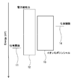
- FIG. 2 is an exemplary energy band diagram of the image sensor shown in FIG. 1A.
- FIG. 3 is a flowchart showing a manufacturing process of the image pickup device shown in FIG. 1A.
- FIG. 4 is a diagram showing an example of a circuit of an imaging device according to an embodiment of the present disclosure.
- FIG. 5 is a cross-sectional view of a unit pixel in the image pickup apparatus according to the embodiment of the present disclosure.
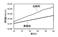
- FIG. 6 is a graph showing the relationship between the voltage applied to the second electrode and the detected current value.
- the image sensor is used in an image pickup device such as a CMOS (Complementary Metal Oxide Semiconductor) image sensor, for example.
- CMOS Complementary Metal Oxide Semiconductor
- a voltage may be applied to the photoelectric conversion layer regardless of whether or not the photoelectric conversion layer is irradiated with light. In this case, electrons flow from the electrodes to the photoelectric conversion layer, and the S / N ratio of the sensor decreases.
- the image sensor according to the first aspect of the present disclosure is With the first electrode With the second electrode A photoelectric conversion layer arranged between the first electrode and the second electrode and converting light into electric charges, An electron blocking layer containing chromium oxide and carbon, which is arranged between the first electrode and the photoelectric conversion layer and suppresses the transfer of electrons from the first electrode to the photoelectric conversion layer. Is equipped with.
- the electron blocking layer may include a plurality of layers.
- the carbon may be contained in the layer containing the oxide of chromium among the plurality of layers.
- the photoelectric conversion layer may contain a photoelectric conversion material, and the photoelectric conversion material may be an organic material. According to the second aspect, it is possible to form the photoelectric conversion layer by directly applying the solution containing the photoelectric conversion material onto the electron blocking layer.
- the photoelectric conversion layer may absorb near infrared light having a wavelength of 780 nm to 2000 nm to generate the charge.
- the image sensor of the third aspect can be used for a sensor that detects near infrared light.
- the absorption peak wavelength of the photoelectric conversion layer may be in the wavelength region of 780 nm to 2000 nm.
- the image sensor of the fourth aspect can be used for a sensor that detects near infrared light.
- the second electrode is such that light is incident from the second electrode toward the photoelectric conversion layer.
- the photoelectric conversion layer, the electron blocking layer, and the first electrode may be arranged in this order. According to this arrangement, the attenuation of the incident light in the electron blocking layer can be suppressed.
- the manufacturing method according to the sixth aspect of the present disclosure is a manufacturing method of an image sensor.
- the image pickup device is arranged between the first electrode, the second electrode, the photoelectric conversion layer arranged between the first electrode and the second electrode, and between the first electrode and the photoelectric conversion layer.
- the electron blocking layer contains chromium oxide and carbon, and contains
- the manufacturing method is Forming the electron blocking layer and Preparing an organic solution containing a photoelectric conversion material and To form the photoelectric conversion layer by applying the organic solution to the electron blocking layer, including.
- the electron blocking layer is hardly damaged.
- a photoelectric conversion layer can be easily formed by applying an organic solution and drying.
- the electron blocking layer may be formed by a metal-organic compound decomposition method.
- the electron blocking layer containing chromium oxide and carbon can be formed with high productivity.
- the image sensor according to the eighth aspect of the present disclosure is with any one of the image sensors of the first to fifth aspects, With the charge storage region electrically connected to the first electrode or the second electrode, A charge detection circuit electrically connected to the charge storage region and Is equipped with.
- the leakage current in the dark can be reduced, improvement in image quality, particularly, improvement in image quality when the amount of light is low can be expected.
- all or part of a circuit, unit, device, member or part, or all or part of a functional block in a block diagram is, for example, a semiconductor device, a semiconductor integrated circuit (IC), or an LSI (range scale integration). ) Can be performed by one or more electronic circuits.
- the LSI or IC may be integrated on one chip, or may be configured by combining a plurality of chips.
- the functional blocks other than the memory element may be integrated on one chip.
- it is called LSI or IC, but the name changes depending on the degree of integration, and it may be called system LSI, VLSI (very large scale integration), or ULSI (ultra large scale integration).
- a Field Programmable Gate Array (FPGA) programmed after the LSI is manufactured, or a reconfigurable logistic device capable of reconfiguring the junction relationship inside the LSI or setting up the circuit partition inside the LSI can also be used for the same purpose.
- FPGA Field Programmable Gate Array
- circuits, units, devices, members or parts can be performed by software processing.
- the software is recorded on a non-temporary recording medium such as one or more ROMs, optical disks, hard disk drives, etc., and when the software is executed by a processor, the functions identified by the software It is performed by a processor and peripherals.
- the system or device may include one or more non-temporary recording media on which the software is recorded, a processor, and the required hardware devices, such as an interface.
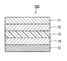
- FIG. 1A shows a cross section of the image sensor 10A according to the embodiment of the present disclosure.
- the image pickup device 10A includes a first electrode 11, an electron blocking layer 12, a photoelectric conversion layer 13, and a second electrode 14.
- the photoelectric conversion layer 13 is arranged between the first electrode 11 and the second electrode 14.
- the electron blocking layer 12 is arranged between the first electrode 11 and the photoelectric conversion layer 13.
- the electron blocking layer 12 is in contact with the first electrode 11 and the photoelectric conversion layer 13.
- the photoelectric conversion layer 13 is in contact with the electron blocking layer 12 and the second electrode 14.
- the first electrode 11, the electron blocking layer 12, the photoelectric conversion layer 13 and the second electrode 14 are laminated in this order.
- the second electrode 14, the photoelectric conversion layer 13, the electron blocking layer 12, and the first electrode 11 are arranged in this order so that light is incident from the second electrode 14 toward the photoelectric conversion layer 13. According to this arrangement, the attenuation of the incident light in the electron blocking layer 12 can be suppressed.
- the image sensor 10A is used, for example, as a part of the pixels of the image sensor.
- the image sensor 10A When the image sensor 10A is irradiated with light, electron-hole pairs are generated in the photoelectric conversion layer 13.
- a voltage is applied between the first electrode 11 and the second electrode 14 so that the potential of the second electrode 14 exceeds the potential of the first electrode 11, holes that are positive charges are transferred to the first electrode 11.
- the collected, negatively charged electrons are collected on the second electrode 14.
- the holes collected in the first electrode 11 or the electrons collected in the second electrode 14 are accumulated in the charge storage region (not shown).
- the electron blocking layer 12 blocks the inflow of electrons from the first electrode 11 to the photoelectric conversion layer 13 in the dark. As a result, the dark current is suppressed, and the S / N ratio, which is the sensitivity of the image sensor 10A, is improved.
- the first electrode 11 plays a role of collecting holes generated in the photoelectric conversion layer 13.
- Examples of the material of the first electrode 11 include metals, metal oxides, metal nitrides, and conductive polysilicon.
- Examples of the metal include aluminum, silver, copper, titanium and tungsten.
- a typical example of a metal nitride is TiN.
- Conductive polysilicon is polysilicon that has been imparted with conductivity by the addition of impurities.
- the first electrode 11 may be a transparent electrode having translucency to visible light and / or near infrared light.
- the first electrode 11 When the first electrode 11 is arranged on the incident side of the light, the light transmitted through the first electrode 11 and the electron blocking layer 12 is incident on the photoelectric conversion layer 13.
- Examples of the material of the transparent electrode include a transparent conductive oxide and a conductive polymer.
- Examples of the transparent conductive oxide include ITO (Indium Tin Oxide), IZO (Indium Zinc Oxide), AZO (Aluminum-doped Zinc Oxide), FTO (Florine-doped Tin Oxide), SnO 2 , TiO 2 , and ZnO 2.
- One or more transparent conductive oxides selected from these can be used as a material for the transparent electrode.
- Examples of the conductive polymer include PEDOT / PSS (poly (3,4-ethireoxythiophene) / poly (4-styrenesulfonic acid)).
- a conductive polymer obtained by dispersing metal particles, transparent conductive oxide particles, or the like in a polymer material can also be used as a material for a transparent electrode.
- having translucency means that the transmittance of light in a specific wavelength region is 60% or more.
- the wavelength region of visible light is a region having a wavelength of 400 nm to 780 nm.
- the wavelength region of near-infrared light is a wavelength region of 780 nm to 2000 nm.
- the transmittance can be calculated by the method specified in Japanese Industrial Standard JIS R3106 (1998).
- the thickness of the first electrode 11 is not particularly limited, and is in the range of, for example, 10 nm to 200 nm.
- the "thickness" is determined by the average value of a plurality of points (for example, any 5 points).
- the thickness of the layer at a specific point can be measured by cutting the image sensor 10A in the thickness direction so as to include the specific point to form a cut surface, and observing the cut surface with an electron microscope.
- the second electrode 14 is an electrode facing the first electrode 11.
- the second electrode 14 plays a role of applying a voltage to the photoelectric conversion layer 13 and collecting electrons generated by the photoelectric conversion layer 13.
- the second electrode 14 has translucency to visible light and / or near-infrared light.
- Examples of the material of the second electrode 14 include a transparent conductive oxide and a conductive polymer.
- Examples of the transparent conductive oxide include ITO, IZO, AZO, FTO, SnO 2 , TiO 2 , ZnO 2 and the like.
- One or more transparent conductive oxides selected from these can be used as the material of the second electrode 14.
- Examples of the conductive polymer include PEDOT / PSS (poly (3,4-ethireoxythiophene) / poly (4-styrenesulfonic acid)).
- a conductive polymer obtained by dispersing metal particles, transparent conductive oxide particles, or the like in a polymer material can also be used as a material for the second electrode 14.
- the second electrode 14 may be a non-transparent electrode having no translucency to visible light and / or near infrared light.
- Examples of the material for the non-transparent electrode include metals, metal oxides, metal nitrides, and conductive polysilicon.
- Examples of the metal include aluminum, silver, copper, titanium and tungsten.
- a typical example of a metal nitride is TiN.
- Conductive polysilicon is polysilicon that has been imparted with conductivity by the addition of impurities.
- the thickness of the second electrode 14 is not particularly limited, and is in the range of, for example, 10 nm to 500 nm.
- the first electrode 11 and the second electrode 14 are also referred to as a pixel electrode and a counter electrode, respectively.
- the first electrode 11, which is a pixel electrode, is electrically connected to the charge storage region. For example, holes are accumulated in the charge storage region.
- the first electrode 11 may be arranged on the incident side of light, and the first electrode 11 may have translucency. In this case, the first electrode 11 becomes a counter electrode, and the second electrode 14 becomes a pixel electrode electrically connected to the charge storage region. Electrons are accumulated in the charge storage region. The type of charge to be stored is selected according to the mobility of carriers in the photoelectric conversion layer 13.
- the electron blocking layer 12 blocks the inflow of electrons from the first electrode 11 to the photoelectric conversion layer 13 to reduce dark current.
- the electron blocking layer 12 contains chromium oxide and carbon.
- a typical example of chromium oxide is Cr 2 O 3 .
- Cr 2 O 3 is a semiconductor having p-type conductivity.
- Cr 2 O 3 has the property of transporting holes and blocking the transport of electrons.
- the electron blocking layer 12 is made of an inorganic material such as Cr 2 O 3 , the manufacturing restrictions of the image sensor 10A are reduced. For example, it is possible to form the photoelectric conversion layer 13 on the electron blocking layer 12 by a coating step using an organic solution.
- chromium oxide may include oxides other than Cr 2 O 3 in the electron blocking layer 12, such as chromium (II) oxide, chromium (IV) oxide, chromium (VI) oxide, and the like. Means that.
- the components contained in the electron blocking layer 12 also depend on the method of forming the electron blocking layer 12. For example, when the electron blocking layer 12 is formed by using an organic compound containing chromium, the organic compound containing chromium may remain in the electron blocking layer 12.
- the main component of the electron blocking layer 12 may be Cr 2 O 3 . "Main component" means the component contained most in the mass ratio.
- the electron blocking layer 12 contains carbon
- the crystallization of the electron blocking layer 12 is suppressed, and the electron blocking layer 12 exhibits a polycrystalline or amorphous state.
- the crystallization of the electron blocking layer 12 is suppressed and the grain boundaries are reduced, the transport of electrons through the grain boundaries is suppressed. That is, the dark current caused by the crystal defect is suppressed.
- the carbon concentration in the electron blocking layer 12 is not particularly limited.
- the carbon concentration in the electron blocking layer 12 is, for example, in the range of 10 atom% or more and 35 atom% or less.
- Elements other than carbon can be considered as impurities to be contained in the electron blocking layer 12. However, elements other than carbon may act as donors or acceptors to the chromium oxides that make up the electron blocking layer 12 and impair the capacity of the electron blocking layer 12. In addition, elements other than carbon may diffuse into the photoelectric conversion layer 13 and adversely affect the characteristics of the photoelectric conversion layer 13.
- Carbon does not function as a donor or acceptor because it is an element of the same family as oxygen, which is one of the main constituent elements of the electron blocking layer 12. Further, when the photoelectric conversion layer 13 is made of an organic material, even if carbon diffuses from the electron blocking layer 12 to the photoelectric conversion layer 13, the characteristics of the photoelectric conversion layer 13 are unlikely to be adversely affected.
- the electron blocking layer 12 may be made of chromium oxide and carbon, in other words, may contain only chromium oxide and carbon. However, the electron blocking layer 12 may contain impurities that are inevitably mixed in during the manufacturing process of the image sensor 10A.
- the thickness of the electron blocking layer 12 is not particularly limited.
- the thickness of the electron blocking layer 12 may be 5 nm or more from the viewpoint of sufficiently reducing the electron tunnel probability.
- the upper limit of the thickness of the electron blocking layer 12 is, for example, 100 nm.
- the carbon content (atom%) in the electron blocking layer 12 can be measured by, for example, X-ray photoelectron spectroscopy (XPS) or secondary ion mass spectrometry (SIMS).
- XPS X-ray photoelectron spectroscopy
- SIMS secondary ion mass spectrometry
- the electron blocking layer 12 has translucency to visible light and / or near infrared light. Although the electron blocking layer 12 contains carbon, its translucency is maintained. Therefore, the direction of light incident on the photoelectric conversion layer 13 is not limited.
- the upper end of the energy band of the electron blocking layer 12 and the photoelectric conversion layer 13 represents the electron affinity, and the lower end represents the ionization potential.
- the electron affinity of the electron blocking layer 12 is smaller than the work function of the first electrode 11.
- the ionization potential of the electron blocking layer 12 is larger than the ionization potential of the photoelectric conversion layer 13. According to such a relationship, the electron blocking layer 12 blocks the passage of electrons and allows the passage of holes.
- the electron affinity and ionization potential of the electron blocking layer 12 mean the electron affinity and ionization potential of the main materials constituting the electron blocking layer 12, respectively.
- the photoelectric conversion layer 13 is a mixed membrane of a donor / acceptor
- the electron affinity and the ionization potential of the photoelectric conversion layer 13 mean the electron affinity of the acceptor and the ionization potential of the donor, respectively.
- the photoelectric conversion layer 13 is irradiated with light to generate electron-hole pairs inside.
- the generated electron-hole pair is separated into electrons and holes by the electric field applied to the photoelectric conversion layer 13, and moves to the first electrode 11 side or the second electrode 14 side according to the electric field, respectively.
- the photoelectric conversion layer 13 may be made of a known photoelectric conversion material.
- the photoelectric conversion material may be an organic material or an inorganic material.
- Examples of the inorganic photoelectric conversion material include hydrogenated amorphous silicon, compound semiconductor materials, and metal oxide semiconductor materials.
- Examples of the compound semiconductor material include CdSe.
- Examples of the metal oxide semiconductor material include ZnO.
- the photoelectric conversion material can typically be an organic material.
- an organic material is used as the photoelectric conversion material, the molecular design of the photoelectric conversion material can be relatively freely performed so that desired photoelectric conversion characteristics can be obtained.
- the photoelectric conversion material is an organic material, the photoelectric conversion layer 13 having excellent flatness can be easily formed by a coating process using a solution containing the photoelectric conversion material.
- the electron blocking layer 12 is made of an inorganic material and the electron blocking layer 12 is hardly dissolved in a solvent, a solution containing a photoelectric conversion material is directly applied onto the electron blocking layer 12. It is possible to form the photoelectric conversion layer 13.
- the photoelectric conversion layer 13 may be composed of a laminated film of a donor material and an acceptor material, or may be composed of a mixed film of these materials.
- the structure of the laminated film of the donor material and the acceptor material is called a heterojunction type.
- the structure of the mixed membrane of the donor material and the acceptor material is called the bulk heterojunction type.
- the p-type semiconductor of an organic compound is a donor organic semiconductor, and mainly refers to an organic compound having a property of easily donating electrons, typified by a hole transporting organic compound. Specifically, it refers to the organic compound having the smaller ionization potential when two organic materials are used in contact with each other. Therefore, as the donor organic semiconductor, any organic compound can be used as long as it is an organic compound having an electron donating property.
- triarylamine compounds for example, triarylamine compounds, benzidine compounds, pyrazoline compounds, styrylamine compounds, hydrazone compounds, triphenylmethane compounds, carbazole compounds, polysilane compounds, thiophene compounds, phthalocyanine compounds, cyanine compounds, merocyanine compounds, oxonor compounds, polyamine compounds, indols.
- a metal complex or the like having a above can be used. Not limited to these, as described above, any organic compound having a smaller ionization potential than the organic compound used as the accepting organic semiconductor may be used as the donor organic semiconductor.
- the n-type semiconductor of an organic compound is an acceptor-type organic semiconductor, which is mainly represented by an electron-transporting organic compound and has a property of easily accepting electrons. Specifically, it refers to the organic compound having the larger electron affinity when two organic compounds are used in contact with each other. Therefore, as the accepting organic compound, any organic compound can be used as long as it is an electron-accepting organic compound. For example, 5 to 7 containing fullerene, fullerene derivative, condensed aromatic carbocyclic compound (naphthalene derivative, anthracene derivative, phenanthrene derivative, tetracene derivative, pyrene derivative, perylene derivative, fluorantene derivative), nitrogen atom, oxygen atom and sulfur atom.
- Heterocyclic compounds eg, pyridine, pyrazine, pyrimidine, pyridazine, triazine, quinoline, quinoxalin, quinazoline, phthalazine, cinnoline, isoquinoline, pteridine, aclysine, phenazine, phenanthroline, tetrazole, pyrazole, imidazole, thiazole, oxazole, indazole, benz.
- pyridine pyrazine, pyrimidine, pyridazine, triazine, quinoline, quinoxalin, quinazoline, phthalazine, cinnoline, isoquinoline, pteridine, aclysine, phenazine, phenanthroline, tetrazole, pyrazole, imidazole, thiazole, oxazole, indazole, benz.
- Imidazole benzotriazole, benzoxazole, benzothiazole, carbazole, purine, triazolopyridazine, triazolopyrimidine, tetrazyneden, oxadiazol, imidazolepyridine, pyrrolidine, pyrrolopyridine, thiadiazolopyridine, dibenzazepine, tribenzazepine, etc.
- Polyarylene compound, fluorene compound, cyclopentadiene compound, silyl compound, metal complex having a nitrogen-containing heterocyclic compound as a ligand, and the like can be used. Not limited to these, as described above, any organic compound having a higher electron affinity than the organic compound used as the donor organic compound may be used as the acceptor organic semiconductor.
- the photoelectric conversion layer 13 may be configured to absorb near-infrared light and perform photoelectric conversion.
- the image sensor 10A can be used as a sensor for detecting near-infrared light.
- the absorption peak wavelength of the photoelectric conversion layer 13 may be in the wavelength region of near infrared light.
- the absorption peak wavelength of the photoelectric conversion layer 13 is, for example, 840 nm or more, 940 nm or more, or 1400 nm or more.
- the wavelengths of 840 nm, 940 nm, and 1400 nm are missing wavelengths of sunlight, and an image sensor provided with a photoelectric conversion layer having an absorption peak wavelength at these wavelengths is not easily affected by sunlight. If such an image sensor is used, it is not easily affected by sunlight day and night under irradiation with near-infrared light, and stable imaging becomes possible.
- the absorption spectrum of the photoelectric conversion layer 13 can be measured using a commercially available spectrophotometer.
- the wavelength range of measurement is, for example, 400 nm to 1200 nm.
- the wavelength of the peak showing the largest absorption coefficient is regarded as the "absorption peak wavelength”.
- the molecular weight of the organic photoelectric conversion material that mainly absorbs the light in the wavelength region of near infrared light is larger than the molecular weight of the organic photoelectric conversion material that mainly absorbs the light in the wavelength region of visible light.
- an organic compound having a conjugated double bond is often used as an organic photoelectric conversion material, and the peak wavelength becomes longer as the conjugated double bond becomes larger. That is, the conjugated double bond and molecular weight of the organic photoelectric conversion material that mainly absorbs the light in the wavelength region of near infrared light are the conjugated double bond and the molecular weight of the organic photoelectric conversion material that mainly absorbs the light in the wavelength region of visible light. And tends to be larger than the molecular weight.
- a thin film of an organic photoelectric conversion material having a large molecular weight is formed by a vacuum vapor deposition method, the organic photoelectric conversion material is easily thermally decomposed.
- the organic photoelectric conversion material can be dissolved in an organic solvent and the photoelectric conversion layer 13 can be formed by the coating method.
- the electron blocking layer 12 is made of an inorganic material, it is difficult to dissolve in an organic solvent. That is, the configuration of the image pickup device 10A of the present embodiment is particularly advantageous when the photoelectric conversion layer 13 is composed of an organic photoelectric conversion material that absorbs light in the wavelength region of near infrared light.
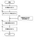
- FIG. 3 shows a manufacturing process of the image sensor 10A.
- the first electrode 11 is formed.
- the first electrode 11 may be formed by a vapor phase film forming method such as a sputtering method, or may be formed by a wet method such as a plating method.
- the first electrode 11 may be formed on a substrate 15 (FIG. 1B) described later or a semiconductor substrate.
- the electron blocking layer 12 is formed on the first electrode 11.
- the method for forming the electron blocking layer 12 is not particularly limited.
- the electron blocking layer 12 can be formed by, for example, a wet method.
- the wet method include a metal-organic compound decomposition method (MOD method: Metal-Organic-Decomposition).
- MOD method Metal-Organic-Decomposition
- a MOD coating agent which is a solution containing a metal organic compound, is applied onto the first electrode 11 to form a coating film.
- the firing conditions of the coating film are, for example, a temperature in the range of 300 ° C. to 600 ° C. and 5 minutes to 1 hour.
- a vapor phase film forming method can be mentioned.
- the crystallinity and carbon concentration of the film can be easily controlled, so that the film is suitable as a method for forming the electron blocking layer 12.
- the vapor phase deposition method include an atomic layer deposition method (ALD method: Atomic Layer Deposition) and a chemical vapor deposition method (CVD method: chemical vapor deposition).
- ALD method Atomic Layer Deposition
- CVD method chemical vapor deposition
- the ALD method and the CVD method are advantageous because the carbon concentration can be controlled more accurately.
- the carbon concentration in the electron blocking layer 12 can be adjusted by changing the conditions such as the raw material and the temperature.
- the electron blocking layer 12 is formed by the ALD method or the CVD method, a metal organic compound containing Cr is used as a raw material gas.
- the electron blocking layer 12 is formed before the photoelectric conversion layer 13 is formed, various methods and materials can be used without being limited by the heat resistance of the organic material constituting the photoelectric conversion layer 13. Can be used to form the electron blocking layer 12.
- step S3 the photoelectric conversion layer 13 is formed on the electron blocking layer 12.
- step S31 an organic solution containing the photoelectric conversion material to form the photoelectric conversion layer 13 is prepared in advance. A coating film is formed by applying this organic solution to the electron blocking layer 12, and a photoelectric conversion layer 13 is formed by drying the coating film.
- the solvent of the organic solution is not particularly limited as long as it can sufficiently dissolve the photoelectric conversion material.
- the electron blocking layer 12 is made of an inorganic material. Therefore, even if the organic solution containing the photoelectric conversion material is directly applied to the electron blocking layer 12, the electron blocking layer 12 is hardly damaged.
- the photoelectric conversion layer 13 can be easily formed by applying an organic solution and drying.
- the second electrode 14 is formed on the photoelectric conversion layer 13.
- the second electrode 14 may be formed by a vapor phase film forming method such as a sputtering method, or may be formed by a wet method such as a plating method.
- the image sensor 10A can be obtained.
- Modification 1B and 1C show cross sections of the image sensors 10B and 10C according to the modified example, respectively.
- the image pickup elements 10B and 10C further include a substrate 15 in addition to the configuration of the image pickup element 10A.
- the first electrode 11 is provided on the substrate 15.
- the first electrode 11, the electron blocking layer 12, the photoelectric conversion layer 13, and the second electrode 14 are laminated on the substrate 15 in this order.
- the second electrode 14 is provided on the substrate 15.
- the second electrode 14, the photoelectric conversion layer 13, the electron blocking layer 12, and the first electrode 11 are laminated on the substrate 15 in this order.
- the substrate 15 plays a role of supporting or protecting the structure including the first electrode 11, the electron blocking layer 12, the photoelectric conversion layer 13, and the second electrode 14.
- the material of the substrate 15 is not particularly limited. Examples of the material of the substrate 15 include glass, quartz, semiconductors, metals, ceramics, and plastics.
- the substrate 15 may have translucency to visible light and / or near-infrared light.
- a hole blocking layer may be provided between the photoelectric conversion layer 13 and the second electrode 14.
- the hole blocking layer blocks the inflow of holes from the second electrode 14 to the photoelectric conversion layer 13.
- the material of the hole blocking layer may be an organic substance, an inorganic substance, or an organic-metal compound.
- the organic substance include copper phthalocyanine, PTCDA (3,4,9,10-perylenetetracarboxylic dianhydride), acetylacetonate complex, BCP, Alq and the like.
- the inorganic substance include MgAg and MgO.
- the hole blocking layer may have a high transmittance so that the absorption of light in the photoelectric conversion layer 13 is not hindered.
- the hole blocking layer may be thin. The thickness of the hole blocking layer is, for example, in the range of 2 nm or more and 50 nm or less.
- the above-mentioned n-type semiconductor or electron-transporting organic compound can also be used.
- FIG. 4 shows an example of the circuit of the image pickup apparatus 100 according to the embodiment of the present disclosure.
- FIG. 5 is a schematic cross-sectional view of the unit pixel 24 in the image pickup apparatus 100 according to the embodiment of the present disclosure.
- the image pickup apparatus 100 includes a semiconductor substrate 40 and a unit pixel 24.
- the unit pixel 24 is a charge detection circuit 35 provided on the semiconductor substrate 40, a photoelectric conversion unit 10 provided on the semiconductor substrate 40, and an electric charge electrically connected to the charge detection circuit 35 and the photoelectric conversion unit 10. It has a storage node 34.
- the image pickup apparatus 100 includes a plurality of unit pixels 24 and peripheral circuits.
- the image pickup apparatus 100 is an organic image sensor realized by a one-chip integrated circuit, and has a pixel array including a plurality of unit pixels 24 arranged two-dimensionally.
- the plurality of unit pixels 24 are arranged two-dimensionally on the semiconductor substrate 40, that is, in the row direction and the column direction, to form a photosensitive region which is a pixel region.
- FIG. 4 shows an example in which the unit pixels 24 are arranged in a matrix of 2 rows and 2 columns.
- the circuit for individually setting the sensitivity of the unit pixel 24 (for example, the pixel electrode control circuit) is not shown.
- the image pickup apparatus 100 may be a line sensor.
- the plurality of unit pixels 24 may be arranged one-dimensionally.
- the row direction and the column direction mean the directions in which the rows and columns extend, respectively. That is, the vertical direction is the column direction and the horizontal direction is the row direction.
- Each unit pixel 24 includes a charge storage node 34 that is electrically connected to the photoelectric conversion unit 10 and the charge detection circuit 35.
- the charge detection circuit 35 includes an amplification transistor 21, a reset transistor 22, and an address transistor 23.
- the photoelectric conversion unit 10 has a first electrode 11 provided as a pixel electrode, an electron blocking layer 12, a photoelectric conversion layer 13, and a second electrode 14 provided as a counter electrode. A predetermined voltage is applied to the second electrode 14 via the counter electrode signal line 26.
- the first electrode 11 is connected to the gate electrode 21G of the amplification transistor 21.
- the signal charge collected by the first electrode 11 is stored in the charge storage node 34 located between the first electrode 11 and the gate electrode 21G of the amplification transistor 21.
- the signal charge is a hole, but the signal charge may be an electron.
- the signal charge accumulated in the charge storage node 34 is applied to the gate electrode 21G of the amplification transistor 21 as a voltage corresponding to the amount of the signal charge.
- the amplification transistor 21 amplifies this voltage and selectively reads it as a signal voltage by the address transistor 23.
- the source electrode or drain electrode of the reset transistor 22 is connected to the first electrode 11, and the signal charge accumulated in the charge storage node 34 is reset. In other words, the reset transistor 22 resets the potentials of the gate electrode 21G and the first electrode 11 of the amplification transistor 21.
- the image pickup apparatus 100 includes a power supply wiring 31, a vertical signal line 27, an address signal line 36, and a reset signal line 37 in order to selectively perform the above-described operation in the plurality of unit pixels 24. These lines are connected to each unit pixel 24, respectively.
- the power supply wiring 31 is connected to the source electrode or the drain electrode of the amplification transistor 21.
- the vertical signal line 27 is connected to the source electrode or drain electrode of the address transistor 23.
- the address signal line 36 is connected to the gate electrode 23G of the address transistor 23.
- the reset signal line 37 is connected to the gate electrode 22G of the reset transistor 22.
- the peripheral circuit includes a vertical scanning circuit 25, a horizontal signal reading circuit 20, a plurality of column signal processing circuits 29, a plurality of load circuits 28, and a plurality of differential amplifiers 32.
- the vertical scanning circuit 25 is also referred to as a row scanning circuit.
- the horizontal signal reading circuit 20 is also referred to as a column scanning circuit.
- the column signal processing circuit 29 is also referred to as a row signal storage circuit.
- the differential amplifier 32 is also referred to as a feedback amplifier.
- the vertical scanning circuit 25 is connected to the address signal line 36 and the reset signal line 37, selects a plurality of unit pixels 24 arranged in each line in line units, reads out the signal voltage, and determines the potential of the first electrode 11. Perform a reset.
- the power supply wiring 31 which is a source follower power supply supplies a predetermined power supply voltage to each unit pixel 24.
- the horizontal signal reading circuit 20 is electrically connected to a plurality of column signal processing circuits 29.
- the column signal processing circuit 29 is electrically connected to the unit pixels 24 arranged in each row via the vertical signal lines 27 corresponding to each row.
- the load circuit 28 is electrically connected to each vertical signal line 27.
- the load circuit 28 and the amplification transistor 21 form a source follower circuit.
- a plurality of differential amplifiers 32 are provided corresponding to each row.
- the negative input terminal of the differential amplifier 32 is connected to the corresponding vertical signal line 27.
- the output terminal of the differential amplifier 32 is connected to the unit pixel 24 via the feedback line 33 corresponding to each row.
- the vertical scanning circuit 25 applies a row selection signal for controlling the on / off of the address transistor 23 to the gate electrode 23G of the address transistor 23 by the address signal line 36. As a result, the line to be read is scanned and selected. A signal voltage is read from the unit pixel 24 of the selected line to the vertical signal line 27.
- the vertical scanning circuit 25 applies a reset signal for controlling the on / off of the reset transistor 22 to the gate electrode 22G of the reset transistor 22 via the reset signal line 37. As a result, the row of the unit pixel 24 that is the target of the reset operation is selected.
- the vertical signal line 27 transmits the signal voltage read from the unit pixel 24 selected by the vertical scanning circuit 25 to the column signal processing circuit 29.
- the column signal processing circuit 29 performs noise suppression signal processing represented by correlated double sampling, analog-to-digital conversion (AD conversion), and the like.
- the horizontal signal reading circuit 20 sequentially reads signals from a plurality of column signal processing circuits 29 to a horizontal common signal line (not shown).
- the differential amplifier 32 is connected to the drain electrode of the reset transistor 22 via the feedback line 33. Therefore, the differential amplifier 32 receives the output value of the address transistor 23 at the negative terminal when the address transistor 23 and the reset transistor 22 are in a conductive state.
- the differential amplifier 32 performs a feedback operation so that the gate potential of the amplification transistor 21 becomes a predetermined feedback voltage. At this time, the output voltage value of the differential amplifier 32 is 0V or a positive voltage in the vicinity of 0V.
- the feedback voltage means the output voltage of the differential amplifier 32.
- the unit pixel 24 includes a semiconductor substrate 40, a charge detection circuit 35, a photoelectric conversion unit 10, and a charge storage node 34.
- the semiconductor substrate 40 may be an insulating substrate or the like in which a semiconductor layer is provided on the surface on the side where the photosensitive region is formed, and is, for example, a p-type silicon substrate.
- the semiconductor substrate 40 has an impurity region (here, an n-type region) 21D, 21S, 22D, 22S and 23S, and an element separation region 41 for electrical separation between the unit pixels 24.
- the element separation region 41 is also provided between the impurity region 21D and the impurity region 22D. As a result, leakage of the signal charge accumulated in the charge storage node 34 is suppressed.
- the device separation region 41 is formed, for example, by implanting acceptor ions under predetermined implantation conditions.
- the impurity regions 21D, 21S, 22D, 22S and 23S are typically diffusion layers formed in the semiconductor substrate 40.
- the amplification transistor 21 includes an impurity region 21S, an impurity region 21D, and a gate electrode 21G.
- the impurity region 21S and the impurity region 21D function as, for example, a source region and a drain region of the amplification transistor 21, respectively.
- a channel region of the amplification transistor 21 is formed between the impurity region 21S and the impurity region 21D.
- the address transistor 23 includes an impurity region 23S, an impurity region 21S, and a gate electrode 23G connected to the address signal line 36.
- the amplification transistor 21 and the address transistor 23 are electrically connected to each other by sharing the impurity region 21S.
- the impurity region 23S functions as, for example, a source region of the address transistor 23.
- the impurity region 23S has a connection with the vertical signal line 27 shown in FIG.
- the reset transistor 22 includes an impurity region 22D, an impurity region 22S, and a gate electrode 22G connected to the reset signal line 37.
- the impurity region 22S functions as, for example, a source region of the reset transistor 22.
- the impurity region 22S has a connection with the reset signal line 37 shown in FIG.
- An interlayer insulating layer 50 is laminated on the semiconductor substrate 40 so as to cover the amplification transistor 21, the address transistor 23, and the reset transistor 22.
- a wiring layer (not shown) may be arranged in the interlayer insulating layer 50.
- the wiring layer is typically made of a metal such as copper and may include, for example, wiring such as the vertical signal line 27 described above.
- the number of layers of the insulating layer in the interlayer insulating layer 50 and the number of layers included in the wiring layer arranged in the interlayer insulating layer 50 can be arbitrarily set.
- a contact plug 54 connected to the impurity region 22D of the reset transistor 22, a contact plug 53 connected to the gate electrode 21G of the amplification transistor 21, and a contact plug 51 connected to the first electrode 11 are included.
- a wiring 52 connecting the contact plug 51, the contact plug 54, and the contact plug 53 is arranged.
- the impurity region 22D of the reset transistor 22 is electrically connected to the gate electrode 21G of the amplification transistor 21.
- the charge detection circuit 35 detects the signal charge captured by the first electrode 11 and outputs the signal voltage.
- the charge detection circuit 35 includes an amplification transistor 21, a reset transistor 22, and an address transistor 23, and is formed on the semiconductor substrate 40.
- the amplification transistor 21 is formed in the semiconductor substrate 40.
- the amplification transistor 21 includes an impurity region 21D that functions as a drain electrode, an impurity region 21S that functions as a gate electrode, a gate insulating layer 21X formed on the semiconductor substrate 40, and a gate electrode formed on the gate insulating layer 21X. Includes 21G and.
- the reset transistor 22 is formed in the semiconductor substrate 40.
- the reset transistor 22 includes an impurity region 22D that functions as a drain electrode, an impurity region 22S that functions as a gate electrode, a gate insulating layer 22X formed on the semiconductor substrate 40, and a gate electrode formed on the gate insulating layer 22X. Includes 22G and.
- the address transistor 23 is formed in the semiconductor substrate 40.
- the address transistor 23 includes an impurity region 21S that functions as a drain electrode, an impurity region 23S that functions as a gate electrode, a gate insulating layer 23X formed on the semiconductor substrate 40, and a gate electrode formed on the gate insulating layer 23X. Includes 23G and.
- the impurity region 21S is shared by the amplification transistor 21 and the address transistor 23, whereby the amplification transistor 21 and the address transistor 23 are connected in series.
- a photoelectric conversion unit 10 is arranged on the interlayer insulating layer 50.
- a plurality of unit pixels 24 constituting the pixel array are formed on the semiconductor substrate 40.
- a plurality of unit pixels 24 arranged two-dimensionally on the semiconductor substrate 40 form a photosensitive region.
- the distance (pixel pitch) between two adjacent unit pixels 24 may be, for example, about 2 ⁇ m.
- the photoelectric conversion unit 10 includes an image pickup device 10A described with reference to FIG. 1A. According to the image sensor 10A, since the leakage current in the dark can be reduced, improvement in image quality, particularly, improvement in image quality when the amount of light is small can be expected. There is a possibility that the dynamic range of the image pickup apparatus 100 can be expanded.
- the charge storage node 34 constitutes a charge storage region electrically connected to the first electrode 11 of the image sensor 10A. Instead of the first electrode 11, the second electrode 14 may be connected to the charge storage node 34.
- a color filter 60 is provided above the photoelectric conversion unit 10.
- a microlens 61 is provided above the color filter 60.
- the color filter 60 is formed as, for example, an on-chip color filter by patterning, and a photosensitive resin or the like in which a dye or a pigment is dispersed is used.
- the microlens 61 is provided as an on-chip microlens, for example, and an ultraviolet photosensitive material or the like is used.
- the image pickup apparatus 100 can be manufactured by using a general semiconductor manufacturing process.
- a silicon substrate is used as the semiconductor substrate 40, it can be manufactured by using various silicon semiconductor processes.
- an image pickup device and an image pickup device having high light absorption characteristics in the wavelength region of near infrared light and capable of exhibiting high photoelectric conversion efficiency it is possible to obtain an image pickup device and an image pickup device having high light absorption characteristics in the wavelength region of near infrared light and capable of exhibiting high photoelectric conversion efficiency.
- An ITO electrode as a first electrode was formed on a glass substrate having a thickness of 0.7 mm.
- the thickness of the ITO electrode was 150 nm.
- a chromium oxide thin film as an electron blocking layer was formed on the ITO electrode by the following method. Specifically, a MOD coating agent (manufactured by High Purity Chemical Laboratory, product number Cr-005) was dropped onto the ITO electrode, and the substrate was rotated at a rotation speed of 3000 rpm for 30 seconds. As a result, a thin film of the MOD coating agent was formed on the ITO electrode. A thin film of the MOD coating agent was heated in the air at 120 ° C. for 10 minutes and then calcined in a nitrogen atmosphere at 400 ° C. for 30 minutes. As a result, a chromium oxide thin film as an electron blocking layer was formed on the ITO electrode. The thickness of the chromium oxide thin film was 15 nm.
- a mixed film of Sn (OSiHex 3 ) 2 Nc and C 60 was formed. Specifically, the mixed film was formed by the vacuum vapor deposition method so that Sn (OSiHex 3 ) 2 Nc and C 60 were contained in the mixed film at a volume ratio of 1: 9. The thickness of the mixed film was 400 nm.
- An Al thin film as a second electrode was formed on the photoelectric conversion layer by a vacuum vapor deposition method.
- the thickness of the Al thin film was 80 nm.
- the second electrode may be a translucent electrode. Both the first electrode and the second electrode may be electrodes having translucency.
- Comparative Example An image sensor of Comparative Example was produced by the same method as in Example except that the electron blocking layer was not formed.
- the leakage current of the image pickup devices of Examples and Comparative Examples was measured by the following method.
- the image sensor was placed in an environment shielded from light, and the measurement terminals of a semiconductor parameter analyzer (manufactured by Keysight, B1500A) were connected to each of the first electrode and the second electrode.
- a voltage of 0 V was applied to the first electrode.
- the voltage applied to the second electrode was swept from 10 V to 20 V, and the current value was measured. The results are shown in FIG.
- FIG. 6 shows the relationship between the voltage applied to the second electrode and the detected current value.
- the current value of the comparative example when 10 V was applied was 2.8 ⁇ 10 -7 mA / cm 2 .
- the current value of the example when 10 V was applied was 1.2 ⁇ 10 -7 mA / cm 2 .
- the current value of the example was significantly lower than the current value of the comparative example.
- the applied voltage was increased to 20 V, the difference between the current value of the comparative example and the current value of the example was further widened.
- the electron blocking layer forms an energy barrier by having a smaller electron affinity than the photoelectric conversion material contained in the photoelectric conversion layer, and suppresses the injection of electrons from the first electrode into the photoelectric conversion layer.
- the electron affinity of Sn (OSiHex 3 ) 2 Nc which is a p-type semiconductor constituting the photoelectric conversion layer, was 4.0 eV.
- the electron affinity of the chromium oxide constituting the electron blocking layer was 2.4 eV. Since an energy barrier of 1.6 eV was formed between the electron affinity of the electron blocking layer and the electron affinity of the photoelectric conversion layer, the electron blocking layer suppressed the injection of electrons from the first electrode into the photoelectric conversion layer, and the leakage current. Is considered to have been reduced.
- the composition ratio of the chromium oxide thin film of the reference example was measured by X-ray photoelectron spectroscopy.
- the chromium oxide thin film contained a sufficient amount of carbon. It is presumed that carbon inhibited the crystallization of the electron blocking layer and suppressed the formation of crystal defects that cause leakage current.
- the technique disclosed in the present specification is useful for an image sensor, and is particularly useful for an image sensor having a photoelectric conversion layer having high light absorption characteristics in the wavelength region of near infrared light.
- the image pickup device can be applied to an image pickup device, an optical sensor, and the like.
Landscapes
- Physics & Mathematics (AREA)
- Electromagnetism (AREA)
- Engineering & Computer Science (AREA)
- Multimedia (AREA)
- Signal Processing (AREA)
- Power Engineering (AREA)
- Condensed Matter Physics & Semiconductors (AREA)
- General Physics & Mathematics (AREA)
- Computer Hardware Design (AREA)
- Microelectronics & Electronic Packaging (AREA)
- Solid State Image Pick-Up Elements (AREA)
Abstract
本開示の一態様に係る撮像素子は、第1電極と、第2電極と、前記第1電極と前記第2電極との間に配置され、光を電荷に変換する光電変換層と、クロムの酸化物及び炭素を含み、前記第1電極と前記光電変換層との間に配置され、前記第1電極から前記光電変換層への電子の移動を抑制する電子ブロッキング層と、を備える。
Description
本開示は、撮像素子、撮像素子の製造方法及び撮像装置に関する。
撮像素子は、第1電極、第2電極及びそれらの間に配置された光電変換層を備えている。第1電極及び第2電極から選ばれる少なくとも1つは透明電極である。光電変換層は、入射した光を吸収して電子-正孔対を生成する。
第1電極と光電変換層との間には、電子ブロッキング層が配置されることがある。電子ブロッキング層は、正孔を通しやすく、電子を通しにくい層である。
特許文献1には、第1電極と光電変換層との間に配置されたバッファ層を備えた撮像素子が記載されている。
撮像素子には、暗時の漏れ電流である暗電流が大きいという特性がある。漏れ電流は撮像素子のS/N比(signal to noise ratio)を低下させるため、漏れ電流を低減することが要望されている。
本開示の一態様に係る撮像素子は、
第1電極と、
第2電極と、
前記第1電極と前記第2電極との間に配置され、光を電荷に変換する光電変換層と、
クロムの酸化物及び炭素を含み、前記第1電極と前記光電変換層との間に配置され、前記第1電極から前記光電変換層への電子の移動を抑制する電子ブロッキング層と、
を備える。
第1電極と、
第2電極と、
前記第1電極と前記第2電極との間に配置され、光を電荷に変換する光電変換層と、
クロムの酸化物及び炭素を含み、前記第1電極と前記光電変換層との間に配置され、前記第1電極から前記光電変換層への電子の移動を抑制する電子ブロッキング層と、
を備える。
本開示によれば、暗時の漏れ電流が小さい撮像素子を提供できる。
(本開示の基礎となった知見)
撮像素子は、例えば、CMOS(Complementary Metal Oxide Semiconductor)イメージセンサなどの撮像装置に使用される。撮像装置においては、光電変換層への光照射の有無によらず、光電変換層に電圧が印加されることがある。この場合、電極から光電変換層に電子が流れ、センサのS/N比が低下する。
撮像素子は、例えば、CMOS(Complementary Metal Oxide Semiconductor)イメージセンサなどの撮像装置に使用される。撮像装置においては、光電変換層への光照射の有無によらず、光電変換層に電圧が印加されることがある。この場合、電極から光電変換層に電子が流れ、センサのS/N比が低下する。
(本開示に係る一態様の概要)
本開示の第1態様に係る撮像素子は、
第1電極と、
前記第2電極と、
前記第1電極と前記第2電極との間に配置され、光を電荷に変換する光電変換層と、
クロムの酸化物及び炭素を含み、前記第1電極と前記光電変換層との間に配置され、前記第1電極から前記光電変換層への電子の移動を抑制する電子ブロッキング層と、
を備えている。
本開示の第1態様に係る撮像素子は、
第1電極と、
前記第2電極と、
前記第1電極と前記第2電極との間に配置され、光を電荷に変換する光電変換層と、
クロムの酸化物及び炭素を含み、前記第1電極と前記光電変換層との間に配置され、前記第1電極から前記光電変換層への電子の移動を抑制する電子ブロッキング層と、
を備えている。
第1態様によれば、暗時の漏れ電流が小さい撮像素子を提供できる。前記電子ブロッキング層は複数の層を含んでいてもよい。前記炭素は、前記複数の層のうち、前記クロムの酸化物を含む層に含まれていてもよい。
本開示の第2態様において、例えば、第1態様に係る撮像素子では、前記光電変換層が光電変換材料を含んでいてもよく、前記光電変換材料が有機材料であってもよい。第2態様によれば、光電変換材料を含む溶液を電子ブロッキング層の上に直接塗布して光電変換層を形成することが可能である。
本開示の第3態様において、例えば、第1又は第2態様に係る撮像素子では、前記光電変換層は、波長が780nmから2000nmの近赤外光を吸収して前記電荷を生成してもよい。第3態様の撮像素子は、近赤外光を検出するセンサに使用されうる。
本開示の第4態様において、例えば、第1から第3態様のいずれか1つに係る撮像素子では、前記光電変換層の吸収ピーク波長が、780nmから2000nmの波長領域にあってもよい。第4態様の撮像素子は、近赤外光を検出するセンサに使用されうる。
本開示の第5態様において、例えば、第1から第4態様のいずれか1つに係る撮像装置では、前記第2電極から前記光電変換層に向けて光が入射するように、前記第2電極、前記光電変換層、前記電子ブロッキング層及び前記第1電極がこの順番で並んでいてもよい。この並びによれば、電子ブロッキング層における入射光の減衰を抑制することができる。
本開示の第6態様に係る製造方法は、撮像素子の製造方法であって、
前記撮像素子は、第1電極と、第2電極と、前記第1電極と前記第2電極との間に配置された光電変換層と、前記第1電極と前記光電変換層との間に配置された電子ブロッキング層と、を備え、
前記電子ブロッキング層は、クロムの酸化物及び炭素を含み、
前記製造方法は、
前記電子ブロッキング層を形成することと、
光電変換材料を含む有機溶液を調製することと、
前記電子ブロッキング層に前記有機溶液を塗布することによって前記光電変換層を形成することと、
を含む。
前記撮像素子は、第1電極と、第2電極と、前記第1電極と前記第2電極との間に配置された光電変換層と、前記第1電極と前記光電変換層との間に配置された電子ブロッキング層と、を備え、
前記電子ブロッキング層は、クロムの酸化物及び炭素を含み、
前記製造方法は、
前記電子ブロッキング層を形成することと、
光電変換材料を含む有機溶液を調製することと、
前記電子ブロッキング層に前記有機溶液を塗布することによって前記光電変換層を形成することと、
を含む。
第6態様によれば、光電変換材料を含む有機溶液を電子ブロッキング層に直接塗布しても電子ブロッキング層がダメージを殆ど受けない。有機溶液の塗布及び乾燥によって光電変換層を容易に形成できる。
本開示の第7態様において、例えば、第6態様に係る撮像素子の製造方法では、前記電子ブロッキング層を金属有機化合物分解法によって形成してもよい。第6態様によれば、高い生産性にて、クロムの酸化物及び炭素を含む電子ブロッキング層を形成することができる。
本開示の第8態様に係る撮像素子は、
第1から第5態様のいずれか1つの撮像素子と、
前記第1電極又は前記第2電極に電気的に接続された電荷蓄積領域と、
前記電荷蓄積領域に電気的に接続された電荷検出回路と、
を備えている。
第1から第5態様のいずれか1つの撮像素子と、
前記第1電極又は前記第2電極に電気的に接続された電荷蓄積領域と、
前記電荷蓄積領域に電気的に接続された電荷検出回路と、
を備えている。
第8態様によれば、暗時の漏れ電流を減らすことができるので、画質の改善、特に、光量が少ないときの画質の改善を期待できる。
本開示において、回路、ユニット、装置、部材または部の全部または一部、またはブロック図における機能ブロックの全部または一部は、例えば、半導体装置、半導体集積回路(IC)、またはLSI(large scale integration)を含む1つまたは複数の電子回路によって実行され得る。LSIまたはICは、1つのチップに集積されてもよいし、複数のチップを組み合わせて構成されてもよい。例えば、記憶素子以外の機能ブロックは、1つのチップに集積されてもよい。ここでは、LSIまたはICと呼んでいるが、集積の度合いによって呼び方が変わり、システムLSI、VLSI(very large scale integration)、もしくはULSI(ultra large scale integration)と呼ばれるものであってもよい。LSIの製造後にプログラムされる、Field Programmable Gate Array(FPGA)、またはLSI内部の接合関係の再構成またはLSI内部の回路区画のセットアップができるreconfigurable logic deviceも同じ目的で使うことができる。
さらに、回路、ユニット、装置、部材または部の全部または一部の機能または動作は、ソフトウェア処理によって実行することが可能である。この場合、ソフトウェアは1つまたは複数のROM、光学ディスク、ハードディスクドライブなどの非一時的記録媒体に記録され、ソフトウェアが処理装置(processor)によって実行されたときに、そのソフトウェアで特定された機能が処理装置(processor)および周辺装置によって実行される。システムまたは装置は、ソフトウェアが記録されている1つまたは複数の非一時的記録媒体、処理装置(processor)、および必要とされるハードウェアデバイス、例えばインターフェースを備えていてもよい。
以下、本開示の実施形態について、図面を参照しながら説明する。本開示は、以下の実施形態に限定されない。
(実施形態)
図1Aは、本開示の一実施形態に係る撮像素子10Aの断面を示している。撮像素子10Aは、第1電極11、電子ブロッキング層12、光電変換層13及び第2電極14を備えている。光電変換層13は、第1電極11と第2電極14との間に配置されている。電子ブロッキング層12は、第1電極11と光電変換層13との間に配置されている。電子ブロッキング層12は、第1電極11と光電変換層13とに接している。光電変換層13は、電子ブロッキング層12と第2電極14とに接している。第1電極11、電子ブロッキング層12、光電変換層13及び第2電極14は、この順番で積層されている。第2電極14から光電変換層13に向けて光が入射するように、第2電極14、光電変換層13、電子ブロッキング層12及び第1電極11がこの順番で並んでいる。この並びによれば、電子ブロッキング層12における入射光の減衰を抑制することができる。
図1Aは、本開示の一実施形態に係る撮像素子10Aの断面を示している。撮像素子10Aは、第1電極11、電子ブロッキング層12、光電変換層13及び第2電極14を備えている。光電変換層13は、第1電極11と第2電極14との間に配置されている。電子ブロッキング層12は、第1電極11と光電変換層13との間に配置されている。電子ブロッキング層12は、第1電極11と光電変換層13とに接している。光電変換層13は、電子ブロッキング層12と第2電極14とに接している。第1電極11、電子ブロッキング層12、光電変換層13及び第2電極14は、この順番で積層されている。第2電極14から光電変換層13に向けて光が入射するように、第2電極14、光電変換層13、電子ブロッキング層12及び第1電極11がこの順番で並んでいる。この並びによれば、電子ブロッキング層12における入射光の減衰を抑制することができる。
撮像素子10Aは、例えば、撮像装置の画素の一部に使用される。撮像素子10Aに光が照射されると、光電変換層13において電子-正孔対が生成する。第2電極14の電位が第1電極11の電位を上回るように第1電極11と第2電極14との間に電圧が印加されると、正の電荷である正孔が第1電極11に集められ、負の電荷である電子が第2電極14に集められる。第1電極11に集められた正孔又は第2電極14に集められた電子が電荷蓄積領域(図示せず)に蓄積される。電子ブロッキング層12は、暗時における第1電極11から光電変換層13への電子の流れ込みを阻止する。これにより、暗電流が抑制され、撮像素子10Aの感度であるS/N比が向上する。
第1電極11は、光電変換層13で生成した正孔を集める役割を担う。第1電極11の材料としては、金属、金属酸化物、金属窒化物、導電性ポリシリコンなどが挙げられる。金属としては、アルミニウム、銀、銅、チタン、タングステンなどが挙げられる。金属窒化物の典型例は、TiNである。導電性ポリシリコンは、不純物の添加によって導電性が付与されたポリシリコンである。
第1電極11は、可視光及び/又は近赤外光に対する透光性を有する透明電極であってもよい。第1電極11が光の入射側に配置された場合、第1電極11及び電子ブロッキング層12を透過した光が光電変換層13に入射する。
透明電極の材料としては、透明導電性酸化物、導電性高分子などが挙げられる。透明導電性酸化物としては、ITO(Indium Tin Oxide)、IZO(Indium Zinc Oxide)、AZO(Aluminum-doped Zinc Oxide)、FTO(Florine-doped Tin Oxide)、SnO2、TiO2、ZnO2などが挙げられる。これらから選ばれる1種又は2種以上の透明導電性酸化物が透明電極の材料として使用されうる。導電性高分子としては、PEDOT/PSS(ポリ(3,4-エチレオキシチオフェン)/ポリ(4-スチレンスルホン酸))が挙げられる。高分子材料に金属粒子、透明導電性酸化物の粒子などを分散させることによって得られた導電性高分子も透明電極の材料として使用可能である。
本明細書において、「透光性を有する」とは、特定の波長領域の光の透過率が60%以上であることを意味する。可視光の波長領域は、波長400nmから780nmの領域である。近赤外光の波長領域は、780nmから2000nmの波長領域である。透過率は、日本工業規格JIS R3106(1998)に規定された方法によって算出されうる。
第1電極11の厚さは特に限定されず、例えば、10nmから200nmの範囲にある。
本明細書において、「厚さ」は、複数の点(例えば、任意の5点)の平均値によって求められる。特定の点における層の厚さは、その特定の点を含むように撮像素子10Aを厚さ方向に切断して切断面を形成し、切断面を電子顕微鏡で観察することによって測定されうる。
第2電極14は、第1電極11に向かい合う電極である。第2電極14は、光電変換層13に電圧を印加するとともに、光電変換層13で生成した電子を集める役割を担う。第2電極14は、可視光及び/又は近赤外光に対する透光性を有する。
第2電極14の材料としては、透明導電性酸化物、導電性高分子などが挙げられる。透明導電性酸化物としては、ITO、IZO、AZO、FTO、SnO2、TiO2、ZnO2などが挙げられる。これらから選ばれる1種又は2種以上の透明導電性酸化物が第2電極14の材料として使用されうる。導電性高分子としては、PEDOT/PSS(ポリ(3,4-エチレオキシチオフェン)/ポリ(4-スチレンスルホン酸))が挙げられる。高分子材料に金属粒子、透明導電性酸化物の粒子などを分散させることによって得られた導電性高分子も第2電極14の材料として使用可能である。
第2電極14は、可視光及び/又は近赤外光に対する透光性を有さない非透明電極であってもよい。
非透明電極の材料としては、金属、金属酸化物、金属窒化物、導電性ポリシリコンなどが挙げられる。金属としては、アルミニウム、銀、銅、チタン、タングステンなどが挙げられる。金属窒化物の典型例は、TiNである。導電性ポリシリコンは、不純物の添加によって導電性が付与されたポリシリコンである。
第2電極14の厚さは特に限定されず、例えば、10nmから500nmの範囲にある。
撮像素子10Aが撮像装置の画素に使用されるとき、第1電極11及び第2電極14は、それぞれ、画素電極及び対向電極とも呼ばれる。画素電極である第1電極11が電荷蓄積領域に電気的に接続される。電荷蓄積領域には例えば正孔が蓄積される。
なお、第1電極11が光の入射側に配置され、第1電極11が透光性を有していてもよい。この場合、第1電極11が対向電極となり、第2電極14が電荷蓄積領域に電気的に接続された画素電極となる。電荷蓄積領域には電子が蓄積される。光電変換層13におけるキャリアの移動度に応じて、蓄積されるべき電荷の種類が選ばれる。
電子ブロッキング層12は、第1電極11から光電変換層13への電子の流れ込みを阻止して暗電流を低減する。電子ブロッキング層12は、クロムの酸化物及び炭素を含む。クロムの酸化物の典型例はCr2O3である。Cr2O3は、p型の導電性を有する半導体である。Cr2O3は、正孔を輸送し、電子の輸送を阻止する特性を有する。Cr2O3のような無機材料で電子ブロッキング層12が構成されている場合、撮像素子10Aの製造上の制約が減少する。例えば、有機溶液を用いた塗布工程によって、電子ブロッキング層12の上に光電変換層13を形成することが可能である。
「クロムの酸化物」の語句は、電子ブロッキング層12がCr2O3以外の酸化物、例えば、酸化クロム(II)、酸化クロム(IV)、酸化クロム(VI)などを含んでいてもよいことを意味する。電子ブロッキング層12に含まれる成分は、電子ブロッキング層12の形成方法にも依存する。例えば、クロムを含む有機化合物を用いて電子ブロッキング層12を形成する場合、電子ブロッキング層12には、クロムを含む有機化合物が残留しうる。電子ブロッキング層12の主成分はCr2O3であってもよい。「主成分」は、質量比で最も多く含まれる成分を意味する。
例えば、電子ブロッキング層12に炭素が含まれている場合、電子ブロッキング層12の結晶化が抑制され、電子ブロッキング層12は、多結晶又はアモルファスの状態を呈する。電子ブロッキング層12の結晶化が抑制されて結晶粒界が減少すると、結晶粒界を介した電子の輸送が抑制される。つまり、結晶欠陥に起因する暗電流が抑制される。電子ブロッキング層12における炭素濃度は特に限定されない。電子ブロッキング層12における炭素濃度は、例えば、10atom%以上35atom%以下の範囲にある。
電子ブロッキング層12に含まれるべき不純物として、炭素以外の元素も考えられる。しかし、炭素以外の元素は、電子ブロッキング層12を構成するクロムの酸化物に対してドナー又はアクセプタとして機能し、電子ブロッキング層12の能力を損なう可能性がある。また、炭素以外の元素は、光電変換層13に拡散して光電変換層13の特性に悪影響を及ぼす可能性がある。
炭素は、電子ブロッキング層12の主要な構成元素の1つである酸素と同族の元素であるため、ドナー又はアクセプタとして機能しない。また、光電変換層13が有機材料で作られている場合、電子ブロッキング層12から光電変換層13に炭素が拡散したとしても、光電変換層13の特性に悪影響が及びにくい。
電子ブロッキング層12は、クロムの酸化物及び炭素からなっていてもよく、言い換えれば、クロムの酸化物及び炭素のみを含んでいてもよい。ただし、撮像素子10Aの製造過程で不可避的に混入する不純物が電子ブロッキング層12に含まれていてもよい。
電子ブロッキング層12の厚さは特に限定されない。電子のトンネル確率を十分に低下させる観点から、電子ブロッキング層12の厚さは、5nm以上であってもよい。電子ブロッキング層12の厚さの上限値は、例えば、100nmである。
電子ブロッキング層12における炭素の含有率(atom%)は、例えば、X線光電子分光(XPS)又は二次イオン質量分析(SIMS)によって測定することができる。
電子ブロッキング層12は、可視光及び/又は近赤外光に対する透光性を有している。電子ブロッキング層12には炭素が含まれているものの、透光性は維持されている。そのため、光電変換層13への光の入射方向は限定されない。
図2は、撮像素子10Aにおける例示的なエネルギーバンドであって、真空準位(=0eV)を基準としたときの電子のポテンシャルを示している。電子ブロッキング層12及び光電変換層13のエネルギーバンドの上端は電子親和力を表し、下端はイオン化ポテンシャルを表す。電子ブロッキング層12の電子親和力は、第1電極11の仕事関数よりも小さい。電子ブロッキング層12のイオン化ポテンシャルは、光電変換層13のイオン化ポテンシャルよりも大きい。このような関係によれば、電子ブロッキング層12は、電子の通過を阻止し、正孔の通過を許容する。
電子ブロッキング層12の電子親和力及びイオン化ポテンシャルは、それぞれ、電子ブロッキング層12を構成する主要な材料の電子親和力及びイオン化ポテンシャルを意味する。光電変換層13がドナー/アクセプタの混合膜の場合、光電変換層13の電子親和力及びイオン化ポテンシャルは、それぞれ、アクセプタの電子親和力及びドナーのイオン化ポテンシャルを意味する。
光電変換層13は、光の照射を受けて内部に電子-正孔対を生成する。生成した電子-正孔対は光電変換層13に加えられた電界によって電子と正孔に分離され、それぞれ電界に従って第1電極11側又は第2電極14側に移動する。
光電変換層13は、公知の光電変換材料によって構成されうる。光電変換材料は、有機材料であってもよく、無機材料であってもよい。無機光電変換材料としては、水素化アモルファスシリコン、化合物半導体材料、金属酸化物半導体材料などが挙げられる。化合物半導体材料としては、CdSeが挙げられる。金属酸化物半導体材料としては、ZnOが挙げられる。
光電変換材料は、典型的には、有機材料でありうる。光電変換材料として有機材料を使用する場合、所望の光電変換特性が得られるように、光電変換材料の分子設計を比較的自由に行える。光電変換材料が有機材料である場合、光電変換材料を含む溶液を用いた塗布プロセスによって平坦化性に優れた光電変換層13を容易に形成することができる。特に、本実施形態によれば、電子ブロッキング層12が無機材料で構成されており、電子ブロッキング層12が溶媒に殆ど溶解しないので、光電変換材料を含む溶液を電子ブロッキング層12の上に直接塗布して光電変換層13を形成することが可能である。
光電変換材料として有機半導体材料を用いる場合、光電変換層13は、ドナー材料とアクセプタ材料との積層膜で構成されていてもよく、これらの材料の混合膜で構成されていてもよい。ドナー材料とアクセプタ材料との積層膜の構造は、ヘテロ接合型と呼ばれる。ドナー材料とアクセプタ材料との混合膜の構造は、バルクヘテロ接合型と呼ばれる。
有機化合物のp型半導体は、ドナー性有機半導体であり、主に、正孔輸送性有機化合物に代表され、電子を供与しやすい性質がある有機化合物をいう。詳しくは、2つの有機材料を接触させて用いたときにイオン化ポテンシャルの小さい方の有機化合物をいう。したがって、ドナー性有機半導体は、電子供与性のある有機化合物であればいずれの有機化合物も使用可能である。例えば、トリアリールアミン化合物、ベンジジン化合物、ピラゾリン化合物、スチリルアミン化合物、ヒドラゾン化合物、トリフェニルメタン化合物、カルバゾール化合物、ポリシラン化合物、チオフェン化合物、フタロシアニン化合物、シアニン化合物、メロシアニン化合物、オキソノール化合物、ポリアミン化合物、インドール化合物、ピロール化合物、ピラゾール化合物、ポリアリーレン化合物、縮合芳香族炭素環化合物(ナフタレン誘導体、アントラセン誘導体、フェナントレン誘導体、テトラセン誘導体、ピレン誘導体、ペリレン誘導体、フルオランテン誘導体)、含窒素ヘテロ環化合物を配位子として有する金属錯体などを用いることができる。これらに限らず、上記したように、アクセプタ性有機半導体として用いた有機化合物よりもイオン化ポテンシャルの小さい有機化合物であればドナー性有機半導体として用いてもよい。
有機化合物のn型半導体は、アクセプタ性有機半導体であり、主に電子輸送性有機化合物に代表され、電子を受容しやすい性質がある有機化合物をいう。詳しくは、2つの有機化合物を接触させて用いたときに電子親和力の大きい方の有機化合物をいう。したがって、アクセプタ性有機化合物は、電子受容性のある有機化合物であればいずれの有機化合物も使用可能である。例えば、フラーレン、フラーレン誘導体、縮合芳香族炭素環化合物(ナフタレン誘導体、アントラセン誘導体、フェナントレン誘導体、テトラセン誘導体、ピレン誘導体、ペリレン誘導体、フルオランテン誘導体)、窒素原子、酸素原子、硫黄原子を含有する5ないし7員のヘテロ環化合物(例えばピリジン、ピラジン、ピリミジン、ピリダジン、トリアジン、キノリン、キノキサリン、キナゾリン、フタラジン、シンノリン、イソキノリン、プテリジン、アクリジン、フェナジン、フェナントロリン、テトラゾール、ピラゾール、イミダゾール、チアゾール、オキサゾール、インダゾール、ベンズイミダゾール、ベンゾトリアゾール、ベンゾオキサゾール、ベンゾチアゾール、カルバゾール、プリン、トリアゾロピリダジン、トリアゾロピリミジン、テトラザインデン、オキサジアゾール、イミダゾピリジン、ピロリジン、ピロロピリジン、チアジアゾロピリジン、ジベンズアゼピン、トリベンズアゼピン等)、ポリアリーレン化合物、フルオレン化合物、シクロペンタジエン化合物、シリル化合物、含窒素ヘテロ環化合物を配位子として有する金属錯体などを用いることができる。これらに限らず、上記したように、ドナー性有機化合物として用いた有機化合物よりも電子親和力の大きい有機化合物であればアクセプタ性有機半導体として用いてよい。
光電変換層13は、近赤外光を吸収して光電変換するように構成されていてもよい。この場合、撮像素子10Aは、近赤外光を検出するセンサに使用されうる。光電変換層13の吸収ピーク波長は、近赤外光の波長領域にあってもよい。光電変換層13の吸収ピーク波長は、例えば840nm以上であり、940nm以上であってもよく、1400nm以上であってもよい。840nm、940nm及び1400nmの波長は、太陽光の欠落波長であり、これらの波長に吸収ピーク波長を有する光電変換層を備えた撮像素子は太陽光の影響を受けにくい。そのような撮像素子を使用すれば、近赤外光の照射下において、昼夜を問わず太陽光の影響を受けにくく、安定した撮像が可能になる。
光電変換層13の吸収スペクトルは、市販の分光光度計を用いて測定することができる。測定の波長範囲は、例えば、400nmから1200nmである。吸収のピークが複数存在するとき、最も大きい吸収係数を示すピークの波長を「吸収ピーク波長」とみなす。
近赤外光の波長領域の光を主に吸収する有機光電変換材料の分子量は、可視光の波長領域の光を主に吸収する有機光電変換材料の分子量よりも大きいという特徴がある。共役二重結合を持つ有機化合物が有機光電変換材料として多く用いられ、共役二重結合が大きくなればなるほどピーク波長が長波長化することが知られている。すなわち、近赤外光の波長領域の光を主に吸収する有機光電変換材料の共役二重結合及び分子量は、可視光の波長領域の光を主に吸収する有機光電変換材料の共役二重結合及び分子量よりも大きい傾向にある。分子量の大きい有機光電変換材料の薄膜を真空蒸着法によって形成する場合、有機光電変換材料が熱分解しやすい。
有機光電変換材料の薄膜を真空蒸着法によって形成できなかったとしても、本実施形態によれば、有機光電変換材料を有機溶媒に溶解させ、塗布法によって光電変換層13を形成することができる。
本実施形態において、電子ブロッキング層12は、無機材料によって構成されているので、有機溶媒に溶解しにくい。つまり、本実施形態の撮像素子10Aの構成は、近赤外光の波長領域の光を吸収する有機光電変換材料によって光電変換層13が構成されている場合に特に有利である。
次に、撮像素子10Aの製造方法を説明する。図3は、撮像素子10Aの製造工程を示している。
ステップS1において、第1電極11を形成する。第1電極11は、スパッタリング法などの気相成膜法によって形成されてもよく、めっき法などの湿式法によって形成されてもよい。第1電極11は、後述する基板15(図1B)又は半導体基板の上に形成されてもよい。
次に、ステップS2において、第1電極11の上に電子ブロッキング層12を形成する。電子ブロッキング層12の形成方法は特に限定されない。電子ブロッキング層12は、例えば、湿式法によって形成することができる。湿式法としては、金属有機化合物分解法(MOD法:Metal-Organic-Decomposition)が挙げられる。具体的には、金属有機化合物を含む溶液であるMODコート剤を第1電極11の上に塗布して塗布膜を形成する。塗布膜を乾燥させ、適切な温度で焼成することによって、高い生産性にて、クロムの酸化物及び炭素を含む電子ブロッキング層を形成することができる。塗布膜の焼成条件は、例えば、300℃から600℃の範囲の温度、及び、5分から1時間である。
電子ブロッキング層12の他の形成方法として、気相成膜法が挙げられる。気相成膜法によれば膜の結晶性及び炭素濃度を制御しやすいので、電子ブロッキング層12の形成方法として適している。気相成膜法としては、原子層堆積法(ALD法:Atomic Layer Deposition)、化学蒸着法(CVD法:chemical vapor deposition)が挙げられる。ALD法及びCVD法は、炭素濃度をより正確に制御しやすいので有利である。ALD法又はCVD法によって電子ブロッキング層12を形成するとき、原料、温度などの条件を変更することによって、電子ブロッキング層12における炭素濃度を調節できる。
ALD法又はCVD法によって電子ブロッキング層12を形成する場合、Crを含む金属有機化合物が原料ガスとして使用される。
本実施形態によれば、光電変換層13を形成する前に電子ブロッキング層12を形成するので、光電変換層13を構成する有機材料の耐熱性に制限されることなく、様々な手法及び材料を用いて電子ブロッキング層12を形成することができる。
次に、ステップS3において、電子ブロッキング層12の上に光電変換層13を形成する。ステップS31において、光電変換層13を構成するべき光電変換材料を含む有機溶液を予め調製する。この有機溶液を電子ブロッキング層12に塗布することによって塗布膜を形成し、塗布膜を乾燥させることによって光電変換層13を形成する。有機溶液の溶媒は、光電変換材料を十分に溶解させることができる溶媒であれば特に限定されない。
本実施形態によれば、電子ブロッキング層12が無機材料によって構成されている。そのため、光電変換材料を含む有機溶液を電子ブロッキング層12に直接塗布しても電子ブロッキング層12がダメージを殆ど受けない。有機溶液の塗布及び乾燥によって光電変換層13を容易に形成できる。
ステップS4において、光電変換層13の上に第2電極14を形成する。第2電極14は、スパッタリング法などの気相成膜法によって形成されてもよく、めっき法などの湿式法によって形成されてもよい。
以上の各工程を実施することによって、撮像素子10Aが得られる。
(変形例)
図1B及び図1Cは、それぞれ、変形例に係る撮像素子10B及び10Cの断面を示している。撮像素子10B及び10Cは、撮像素子10Aの構成に加え、基板15をさらに備えている。
図1B及び図1Cは、それぞれ、変形例に係る撮像素子10B及び10Cの断面を示している。撮像素子10B及び10Cは、撮像素子10Aの構成に加え、基板15をさらに備えている。
撮像素子10Bにおいて、基板15の上に第1電極11が設けられている。基板15の上に第1電極11、電子ブロッキング層12、光電変換層13及び第2電極14がこの順番で積層されている。
撮像素子10Cにおいて、基板15の上に第2電極14が設けられている。基板15の上に第2電極14、光電変換層13、電子ブロッキング層12及び第1電極11がこの順番で積層されている。
基板15は、第1電極11、電子ブロッキング層12、光電変換層13及び第2電極14を含む構造体を支持又は保護する役割を担う。基板15の材料は特に限定されない。基板15の材料として、ガラス、石英、半導体、金属、セラミック、プラスチックなどが挙げられる。基板15は、可視光及び/又は近赤外光に対する透光性を有していてもよい。
撮像素子10A,10B及び10Cにおいて、光電変換層13と第2電極14との間に正孔ブロッキング層が設けられていてもよい。正孔ブロッキング層は、第2電極14から光電変換層13への正孔の流れ込みを阻止する。
正孔ブロッキング層の材料は、有機物であってもよく、無機物であってもよく、有機-金属化合物であってもよい。有機物としては、銅フタロシアニン、PTCDA(3,4,9,10-ペリレンテトラカルボン酸二無水物)、アセチルアセトネート錯体、BCP、Alqなどが挙げられる。無機物としては、MgAg、MgOなどが挙げられる。光電変換層13における光の吸収が妨げられないように、正孔ブロッキング層は、高い透過率を有していてもよい。正孔ブロッキング層は薄くてもよい。正孔ブロッキング層の厚さは、例えば、2nm以上50nm以下の範囲にある。正孔ブロッキング層の材料として、上述のn型半導体又は電子輸送性有機化合物を用いることもできる。
[撮像装置]
図4は、本開示の一実施形態に係る撮像装置100の回路の一例を示している。図5は、本開示の一実施形態に係る撮像装置100における単位画素24の概略断面図である。
図4は、本開示の一実施形態に係る撮像装置100の回路の一例を示している。図5は、本開示の一実施形態に係る撮像装置100における単位画素24の概略断面図である。
本実施形態に係る撮像装置100は、半導体基板40及び単位画素24を備えている。単位画素24は、半導体基板40に設けられた電荷検出回路35、半導体基板40上に設けられた光電変換部10、及び、電荷検出回路35と光電変換部10とに電気的に接続された電荷蓄積ノード34を有する。
図4に示すように、撮像装置100は、複数の単位画素24と周辺回路とを備えている。撮像装置100は、1チップの集積回路で実現される有機イメージセンサであり、2次元に配列された複数の単位画素24を含む画素アレイを有する。
複数の単位画素24は、半導体基板40上に2次元、すなわち行方向及び列方向に配列されて、画素領域である感光領域を形成している。図4は、単位画素24が2行2列のマトリクス状に配列された例を示している。図4では、図示の便宜上、単位画素24の感度を個別に設定するための回路(例えば、画素電極制御回路)の図示を省略している。撮像装置100は、ラインセンサであってもよい。その場合、複数の単位画素24は、1次元に配列されていてもよい。本明細書において、行方向及び列方向とは、行及び列がそれぞれ延びる方向をいう。つまり、垂直方向が列方向であり、水平方向が行方向である。
各単位画素24は、光電変換部10と電荷検出回路35とに電気的に接続された電荷蓄積ノード34を含む。電荷検出回路35は、増幅トランジスタ21と、リセットトランジスタ22と、アドレストランジスタ23とを含む。
光電変換部10は、画素電極として設けられた第1電極11、電子ブロッキング層12、光電変換層13、及び、対向電極として設けられた第2電極14を有する。第2電極14には、対向電極信号線26を介して所定の電圧が印加される。
第1電極11は、増幅トランジスタ21のゲート電極21Gに接続されている。第1電極11によって集められた信号電荷は、第1電極11と増幅トランジスタ21のゲート電極21Gとの間に位置する電荷蓄積ノード34に蓄積される。本実施形態では、信号電荷は正孔であるが、信号電荷は電子であってもよい。
電荷蓄積ノード34に蓄積された信号電荷は、信号電荷の量に応じた電圧として増幅トランジスタ21のゲート電極21Gに印加される。増幅トランジスタ21は、この電圧を増幅し、信号電圧として、アドレストランジスタ23によって、選択的に読み出される。リセットトランジスタ22は、そのソース電極又はドレイン電極が第1電極11に接続されており、電荷蓄積ノード34に蓄積された信号電荷をリセットする。換言すると、リセットトランジスタ22は、増幅トランジスタ21のゲート電極21G及び第1電極11の電位をリセットする。
複数の単位画素24において上述した動作を選択的に行うために、撮像装置100は、電源配線31と、垂直信号線27と、アドレス信号線36と、リセット信号線37とを有する。これらの線が各単位画素24にそれぞれ接続されている。具体的には、電源配線31は、増幅トランジスタ21のソース電極又はドレイン電極に接続されている。垂直信号線27は、アドレストランジスタ23のソース電極又はドレイン電極に接続されている。アドレス信号線36はアドレストランジスタ23のゲート電極23Gに接続されている。リセット信号線37は、リセットトランジスタ22のゲート電極22Gに接続されている。
周辺回路は、垂直走査回路25と、水平信号読出し回路20と、複数のカラム信号処理回路29と、複数の負荷回路28と、複数の差動増幅器32とを含む。垂直走査回路25は行走査回路とも称される。水平信号読出し回路20は列走査回路とも称される。カラム信号処理回路29は行信号蓄積回路とも称される。差動増幅器32はフィードバックアンプとも称される。
垂直走査回路25は、アドレス信号線36及びリセット信号線37に接続されており、各行に配置された複数の単位画素24を行単位で選択し、信号電圧の読出し及び第1電極11の電位のリセットを行う。ソースフォロア電源である電源配線31は、各単位画素24に所定の電源電圧を供給する。水平信号読出し回路20は、複数のカラム信号処理回路29に電気的に接続されている。カラム信号処理回路29は、各列に対応した垂直信号線27を介して、各列に配置された単位画素24に電気的に接続されている。負荷回路28は、各垂直信号線27に電気的に接続されている。負荷回路28と増幅トランジスタ21とは、ソースフォロア回路を形成する。
複数の差動増幅器32は、各列に対応して設けられている。差動増幅器32の負側の入力端子は、対応した垂直信号線27に接続されている。差動増幅器32の出力端子は、各列に対応したフィードバック線33を介して単位画素24に接続されている。
垂直走査回路25は、アドレス信号線36によって、アドレストランジスタ23のオン及びオフを制御する行選択信号をアドレストランジスタ23のゲート電極23Gに印加する。これにより、読出し対象の行が走査され、選択される。選択された行の単位画素24から垂直信号線27に信号電圧が読み出される。垂直走査回路25は、リセット信号線37を介して、リセットトランジスタ22のオン及びオフを制御するリセット信号をリセットトランジスタ22のゲート電極22Gに印加する。これにより、リセット動作の対象となる単位画素24の行が選択される。垂直信号線27は、垂直走査回路25によって選択された単位画素24から読み出された信号電圧をカラム信号処理回路29へ伝達する。
カラム信号処理回路29は、相関二重サンプリングに代表される雑音抑圧信号処理及びアナログ-デジタル変換(AD変換)などを行う。
水平信号読出し回路20は、複数のカラム信号処理回路29から水平共通信号線(不図示)に信号を順次読み出す。
差動増幅器32は、フィードバック線33を介してリセットトランジスタ22のドレイン電極に接続されている。したがって、差動増幅器32は、アドレストランジスタ23とリセットトランジスタ22とが導通状態にあるときに、アドレストランジスタ23の出力値を負端子に受ける。増幅トランジスタ21のゲート電位が所定のフィードバック電圧となるように、差動増幅器32はフィードバック動作を行う。このとき、差動増幅器32の出力電圧値は、0V又は0V近傍の正電圧である。フィードバック電圧とは、差動増幅器32の出力電圧を意味する。
図5に示すように、単位画素24は、半導体基板40と、電荷検出回路35と、光電変換部10と、電荷蓄積ノード34とを含む。
半導体基板40は、感光領域が形成される側の表面に半導体層が設けられた絶縁性基板等であってもよく、例えば、p型シリコン基板である。半導体基板40は、不純物領域(ここではn型領域)21D,21S,22D,22S及び23Sと、単位画素24間の電気的な分離のための素子分離領域41と、を有する。ここでは、素子分離領域41は、不純物領域21Dと不純物領域22Dとの間にも設けられている。これにより、電荷蓄積ノード34に蓄積された信号電荷のリークが抑制される。なお、素子分離領域41は、例えば、所定の注入条件の下でアクセプタのイオン注入を行うことによって形成される。
不純物領域21D,21S,22D,22S及び23Sは、典型的には、半導体基板40内に形成された拡散層である。図5に示すように、増幅トランジスタ21は、不純物領域21Sと、不純物領域21Dと、ゲート電極21Gと、を含む。不純物領域21S及び不純物領域21Dは、それぞれ、増幅トランジスタ21の例えばソース領域及びドレイン領域として機能する。不純物領域21S及び不純物領域21Dの間に、増幅トランジスタ21のチャネル領域が形成される。
同様に、アドレストランジスタ23は、不純物領域23Sと、不純物領域21Sと、アドレス信号線36に接続されたゲート電極23Gと、を含む。この例では、増幅トランジスタ21及びアドレストランジスタ23は、不純物領域21Sを共有することによって互いに電気的に接続されている。不純物領域23Sは、アドレストランジスタ23の例えばソース領域として機能する。不純物領域23Sは、図4に示す垂直信号線27との接続を有する。
リセットトランジスタ22は、不純物領域22D、不純物領域22Sと、リセット信号線37に接続されたゲート電極22Gと、を含む。不純物領域22Sは、リセットトランジスタ22の例えばソース領域として機能する。不純物領域22Sは、図4に示すリセット信号線37との接続を有する。
半導体基板40上には、増幅トランジスタ21、アドレストランジスタ23及びリセットトランジスタ22を覆うように層間絶縁層50が積層されている。
層間絶縁層50中には、配線層(図示せず)が配置されうる。配線層は、典型的には、銅などの金属から形成され、例えば、上述の垂直信号線27などの配線をその一部に含みうる。層間絶縁層50中の絶縁層の層数、及び、層間絶縁層50中に配置される配線層に含まれる層数は、任意に設定可能である。
層間絶縁層50中には、リセットトランジスタ22の不純物領域22Dと接続されたコンタクトプラグ54、増幅トランジスタ21のゲート電極21Gと接続されたコンタクトプラグ53、第1電極11と接続されたコンタクトプラグ51、及びコンタクトプラグ51とコンタクトプラグ54とコンタクトプラグ53とを接続する配線52が配置されている。これにより、リセットトランジスタ22の不純物領域22Dが増幅トランジスタ21のゲート電極21Gと電気的に接続されている。
電荷検出回路35は、第1電極11によって捕捉された信号電荷を検出し、信号電圧を出力する。電荷検出回路35は、増幅トランジスタ21と、リセットトランジスタ22と、アドレストランジスタ23とを含み、半導体基板40に形成されている。
増幅トランジスタ21は、半導体基板40内に形成されている。増幅トランジスタ21は、ドレイン電極として機能する不純物領域21Dと、ゲート電極として機能する不純物領域21Sと、半導体基板40上に形成されたゲート絶縁層21Xと、ゲート絶縁層21X上に形成されたゲート電極21Gと、を含む。
リセットトランジスタ22は、半導体基板40内に形成されている。リセットトランジスタ22は、ドレイン電極として機能する不純物領域22Dと、ゲート電極として機能する不純物領域22Sと、半導体基板40上に形成されたゲート絶縁層22Xと、ゲート絶縁層22X上に形成されたゲート電極22Gと、を含む。
アドレストランジスタ23は、半導体基板40内に形成されている。アドレストランジスタ23は、ドレイン電極として機能する不純物領域21Sと、ゲート電極として機能する不純物領域23Sと、半導体基板40上に形成されたゲート絶縁層23Xと、ゲート絶縁層23X上に形成されたゲート電極23Gと、を含む。不純物領域21Sは、増幅トランジスタ21とアドレストランジスタ23とに共用されており、これにより、増幅トランジスタ21とアドレストランジスタ23とが直列に接続される。
層間絶縁層50上には、光電変換部10が配置されている。換言すれば、本実施形態では、画素アレイを構成する複数の単位画素24が、半導体基板40上に形成されている。半導体基板40上に2次元に配列された複数の単位画素24は、感光領域を形成する。隣接する2つの単位画素24間の距離(画素ピッチ)は、例えば2μm程度であってもよい。
光電変換部10は、図1Aを参照して説明した撮像素子10Aを含む。撮像素子10Aによれば、暗時の漏れ電流を減らすことができるので、画質の改善、特に、光量が少ないときの画質の改善を期待できる。撮像装置100のダイナミックレンジを拡大できる可能性もある。
電荷蓄積ノード34は、撮像素子10Aの第1電極11に電気的に接続された電荷蓄積領域を構成している。第1電極11に代えて、第2電極14が電荷蓄積ノード34に接続されることもある。
光電変換部10の上方には、カラーフィルタ60が設けられている。カラーフィルタ60の上方にマイクロレンズ61が設けられている。カラーフィルタ60は、例えば、パターニングによるオンチップカラーフィルタとして形成され、染料又は顔料が分散された感光性樹脂等が用いられる。マイクロレンズ61は、例えば、オンチップマイクロレンズとして設けられ、紫外線感光材等が用いられる。
撮像装置100は、一般的な半導体製造プロセスを用いて製造することができる。特に、半導体基板40としてシリコン基板を用いる場合には、種々のシリコン半導体プロセスを利用することによって製造することができる。
以上から、本実施形態によれば、近赤外光の波長領域に高い光吸収特性を有し、かつ高い光電変換効率を発現することが可能な撮像素子及び撮像装置を得ることができる。
(実施例)
厚さ0.7mmのガラス基板の上に第1電極としてのITO電極を形成した。ITO電極の厚さは150nmであった。
厚さ0.7mmのガラス基板の上に第1電極としてのITO電極を形成した。ITO電極の厚さは150nmであった。
次に、ITO電極の上に電子ブロッキング層としてのクロム酸化物薄膜を以下の方法によって形成した。具体的には、MODコート剤(高純度化学研究所製、品番Cr-005)をITO電極に滴下し、基板を3000rpmの回転数で30秒間回転させた。これにより、ITO電極の上にMODコート剤の薄膜を形成した。MODコート剤の薄膜を120℃の大気中で10分間加熱した後、さらに、400℃の窒素雰囲気中で30分間焼成した。これにより、ITO電極の上に電子ブロッキング層としてのクロム酸化物薄膜を形成した。クロム酸化物薄膜の厚さは15nmであった。
次に、光電変換層として、Sn(OSiHex3)2NcとC60との混合膜を形成した。具体的には、真空蒸着法によって、Sn(OSiHex3)2NcとC60とが1:9の体積比で混合膜に含まれるように、真空蒸着法によって混合膜を形成した。混合膜の厚さは400nmであった。
真空蒸着法によって、第2電極としてのAl薄膜を光電変換層の上に形成した。Al薄膜の厚さは厚さ80nmであった。以上の工程を経て、サンプル1の撮像素子を作製した。
第1電極に代えて、第2電極が透光性を有する電極であってもよい。第1電極及び第2電極の両方が透光性を有する電極であってもよい。
(参照例)
実施例と同じ方法によって、Siウエハ上に厚さ15nmのクロム酸化物薄膜を形成した。これにより、クロム酸化物薄膜の分析用のサンプルを得た。
実施例と同じ方法によって、Siウエハ上に厚さ15nmのクロム酸化物薄膜を形成した。これにより、クロム酸化物薄膜の分析用のサンプルを得た。
(比較例)
電子ブロッキング層を形成しなかったことを除き、実施例と同じ方法で比較例の撮像素子を作製した。
電子ブロッキング層を形成しなかったことを除き、実施例と同じ方法で比較例の撮像素子を作製した。
[暗時における漏れ電流特性]
実施例及び比較例の撮像素子の漏れ電流を以下の方法で測定した。撮像素子を光から遮断した環境下に置き、第1電極及び第2電極のそれぞれに半導体パラメータアナライザ(Keysight社製、B1500A)の測定端子を接続した。第1電極に0Vの電圧を印加した。第2電極への印加電圧を10Vから20Vまで掃引させて電流値を測定した。結果を図6に示す。
実施例及び比較例の撮像素子の漏れ電流を以下の方法で測定した。撮像素子を光から遮断した環境下に置き、第1電極及び第2電極のそれぞれに半導体パラメータアナライザ(Keysight社製、B1500A)の測定端子を接続した。第1電極に0Vの電圧を印加した。第2電極への印加電圧を10Vから20Vまで掃引させて電流値を測定した。結果を図6に示す。
図6は、第2電極への印加電圧と検出された電流値との関係を示している。10V印加時の比較例の電流値は2.8×10⁻⁷mA/cm2であった。10V印加時の実施例の電流値は1.2×10-7mA/cm2であった。10V印加時において、実施例の電流値は、比較例の電流値を大幅に下回った。印加電圧を20Vまで増加させたとき、比較例の電流値と実施例の電流値との差は更に拡大した。
電子ブロッキング層は、光電変換層に含まれた光電変換材料よりも小さい電子親和力を有することによってエネルギー障壁を形成し、第1電極から光電変換層への電子の注入を抑制する。光電変換層を構成するp型半導体であるSn(OSiHex3)2Ncの電子親和力は4.0eVであった。電子ブロッキング層を構成するクロム酸化物の電子親和力は2.4eVであった。電子ブロッキング層の電子親和力と光電変換層の電子親和力との間に1.6eVのエネルギー障壁が形成されたため、電子ブロッキング層によって第1電極から光電変換層への電子の注入が抑制され、漏れ電流が低減されたと考えられる。
参照例のクロム酸化物薄膜の組成比をX線光電子分光法によって測定した。組成比は、Cr:O:C:N=0.23:0.42:0.34:0.01であった。クロム酸化物薄膜には、十分な量の炭素が含まれていた。炭素が電子ブロッキング層の結晶化を阻害し、漏れ電流の原因となる結晶欠陥の生成を抑制したと推測される。
本明細書に開示された技術は、撮像素子に有用であり、特に、近赤外光の波長領域において高い光吸収特性を有する光電変換層を備えた撮像素子に有用である。撮像素子は、撮像装置、光センサなどに応用されうる。
10A,10B,10C 撮像素子
11 第1電極
12 電子ブロッキング層
13 光電変換層
14 第2電極
15 基板
24 単位画素
34 電荷蓄積ノード
35 電荷検出回路
100 撮像装置
11 第1電極
12 電子ブロッキング層
13 光電変換層
14 第2電極
15 基板
24 単位画素
34 電荷蓄積ノード
35 電荷検出回路
100 撮像装置
Claims (8)
- 第1電極と、
第2電極と、
前記第1電極と前記第2電極との間に配置され、光を電荷に変換する光電変換層と、
クロムの酸化物及び炭素を含み、前記第1電極と前記光電変換層との間に配置され、前記第1電極から前記光電変換層への電子の移動を抑制する電子ブロッキング層と、
を備えた、
撮像素子。 - 前記光電変換層が光電変換材料を含み、
前記光電変換材料が有機材料である、
請求項1に記載の撮像素子。 - 前記光電変換層は、波長が780nmから2000nmの近赤外光を吸収して前記電荷を生成する、
請求項1又は2に記載の撮像素子。 - 前記光電変換層の吸収ピーク波長が、780nmから2000nmの波長領域にある、
請求項1から3のいずれか1項に記載の撮像素子。 - 前記第2電極から前記光電変換層に向けて光が入射するように、前記第2電極、前記光電変換層、前記電子ブロッキング層及び前記第1電極がこの順番で並んでいる、
請求項1から4のいずれか1項に記載の撮像素子。 - 撮像素子の製造方法であって、
前記撮像素子は、第1電極と、第2電極と、前記第1電極と前記第2電極との間に配置された光電変換層と、前記第1電極と前記光電変換層との間に配置された電子ブロッキング層と、を備え、
前記電子ブロッキング層は、クロムの酸化物及び炭素を含み、
前記製造方法は、
前記電子ブロッキング層を形成することと、
光電変換材料を含む有機溶液を調製することと、
前記電子ブロッキング層に前記有機溶液を塗布することによって前記光電変換層を形成することと、
を含む、
撮像素子の製造方法。 - 前記電子ブロッキング層を金属有機化合物分解法によって形成する、
請求項6に記載の撮像素子の製造方法。 - 請求項1から5のいずれか1項に記載の撮像素子と、
前記第1電極又は前記第2電極に電気的に接続された電荷蓄積領域と、
前記電荷蓄積領域に電気的に接続された電荷検出回路と、
を備えた、
撮像装置。
Priority Applications (2)
| Application Number | Priority Date | Filing Date | Title |
|---|---|---|---|
| JP2021505602A JPWO2020184016A1 (ja) | 2019-03-12 | 2020-02-07 | |
| US17/324,181 US20210273020A1 (en) | 2019-03-12 | 2021-05-19 | Imaging device, method for manufacturing imaging device, and imaging apparatus |
Applications Claiming Priority (2)
| Application Number | Priority Date | Filing Date | Title |
|---|---|---|---|
| JP2019044761 | 2019-03-12 | ||
| JP2019-044761 | 2019-03-12 |
Related Child Applications (1)
| Application Number | Title | Priority Date | Filing Date |
|---|---|---|---|
| US17/324,181 Continuation US20210273020A1 (en) | 2019-03-12 | 2021-05-19 | Imaging device, method for manufacturing imaging device, and imaging apparatus |
Publications (1)
| Publication Number | Publication Date |
|---|---|
| WO2020184016A1 true WO2020184016A1 (ja) | 2020-09-17 |
Family
ID=72427877
Family Applications (1)
| Application Number | Title | Priority Date | Filing Date |
|---|---|---|---|
| PCT/JP2020/004774 WO2020184016A1 (ja) | 2019-03-12 | 2020-02-07 | 撮像素子、撮像素子の製造方法及び撮像装置 |
Country Status (3)
| Country | Link |
|---|---|
| US (1) | US20210273020A1 (ja) |
| JP (1) | JPWO2020184016A1 (ja) |
| WO (1) | WO2020184016A1 (ja) |
Citations (4)
| Publication number | Priority date | Publication date | Assignee | Title |
|---|---|---|---|---|
| JP2003163360A (ja) * | 2000-12-07 | 2003-06-06 | Seiko Epson Corp | 光電変換素子 |
| JP2010003901A (ja) * | 2008-06-20 | 2010-01-07 | Fujifilm Corp | 光電変換素子及び固体撮像素子 |
| JP2010114181A (ja) * | 2008-11-05 | 2010-05-20 | Konica Minolta Holdings Inc | 有機光電変換素子、及びその製造方法 |
| JP2011222949A (ja) * | 2010-03-24 | 2011-11-04 | Fujifilm Corp | 光電変換素子及び撮像素子 |
Family Cites Families (1)
| Publication number | Priority date | Publication date | Assignee | Title |
|---|---|---|---|---|
| US9754980B2 (en) * | 2015-06-30 | 2017-09-05 | Semiconductor Energy Laboratory Co., Ltd. | Photoelectric conversion element and imaging device |
-
2020
- 2020-02-07 JP JP2021505602A patent/JPWO2020184016A1/ja active Pending
- 2020-02-07 WO PCT/JP2020/004774 patent/WO2020184016A1/ja active Application Filing
-
2021
- 2021-05-19 US US17/324,181 patent/US20210273020A1/en active Pending
Patent Citations (4)
| Publication number | Priority date | Publication date | Assignee | Title |
|---|---|---|---|---|
| JP2003163360A (ja) * | 2000-12-07 | 2003-06-06 | Seiko Epson Corp | 光電変換素子 |
| JP2010003901A (ja) * | 2008-06-20 | 2010-01-07 | Fujifilm Corp | 光電変換素子及び固体撮像素子 |
| JP2010114181A (ja) * | 2008-11-05 | 2010-05-20 | Konica Minolta Holdings Inc | 有機光電変換素子、及びその製造方法 |
| JP2011222949A (ja) * | 2010-03-24 | 2011-11-04 | Fujifilm Corp | 光電変換素子及び撮像素子 |
Also Published As
| Publication number | Publication date |
|---|---|
| US20210273020A1 (en) | 2021-09-02 |
| JPWO2020184016A1 (ja) | 2020-09-17 |
Similar Documents
| Publication | Publication Date | Title |
|---|---|---|
| JP5087304B2 (ja) | 固体撮像素子の製造方法 | |
| US10861904B2 (en) | Imaging device including a photoelectric converter and a voltage application circuit | |
| JP2016225456A (ja) | 撮像装置および光電変換膜の製造方法 | |
| WO2020162095A1 (ja) | 光電変換素子および撮像装置 | |
| JP7190715B2 (ja) | 撮像装置 | |
| JP2018125495A (ja) | 光電変換素子および撮像装置 | |
| US11711932B2 (en) | Photoelectric conversion element including first electrode, second electrodes, photoelectric conversion film, and conductive layer and method for manufacturing the same | |
| WO2020184015A1 (ja) | 撮像素子、撮像素子の製造方法及び撮像装置 | |
| US20230045630A1 (en) | Imaging device | |
| WO2020184016A1 (ja) | 撮像素子、撮像素子の製造方法及び撮像装置 | |
| WO2021149414A1 (ja) | 撮像装置 | |
| WO2021149413A1 (ja) | 撮像装置 | |
| US11723224B2 (en) | Imaging apparatus | |
| WO2023074230A1 (ja) | 撮像装置 | |
| US20230283927A1 (en) | Imaging device and driving method | |
| WO2022149401A1 (ja) | 撮像装置 | |
| WO2021220691A1 (ja) | 光電変換素子および撮像装置 | |
| WO2023140013A1 (ja) | 光電変換素子、撮像装置およびフラーレン誘導体溶液 | |
| CN118104414A (zh) | 摄像装置 |
Legal Events
| Date | Code | Title | Description |
|---|---|---|---|
| 121 | Ep: the epo has been informed by wipo that ep was designated in this application |
Ref document number: 20771061 Country of ref document: EP Kind code of ref document: A1 |
|
| ENP | Entry into the national phase |
Ref document number: 2021505602 Country of ref document: JP Kind code of ref document: A |
|
| NENP | Non-entry into the national phase |
Ref country code: DE |
|
| 122 | Ep: pct application non-entry in european phase |
Ref document number: 20771061 Country of ref document: EP Kind code of ref document: A1 |