WO2020183843A1 - 制御回路および測距システム - Google Patents
制御回路および測距システム Download PDFInfo
- Publication number
- WO2020183843A1 WO2020183843A1 PCT/JP2019/049482 JP2019049482W WO2020183843A1 WO 2020183843 A1 WO2020183843 A1 WO 2020183843A1 JP 2019049482 W JP2019049482 W JP 2019049482W WO 2020183843 A1 WO2020183843 A1 WO 2020183843A1
- Authority
- WO
- WIPO (PCT)
- Prior art keywords
- power supply
- unit
- transistor
- voltage
- supply voltage
- Prior art date
- Legal status (The legal status is an assumption and is not a legal conclusion. Google has not performed a legal analysis and makes no representation as to the accuracy of the status listed.)
- Ceased
Links
Images




Classifications
-
- G—PHYSICS
- G01—MEASURING; TESTING
- G01S—RADIO DIRECTION-FINDING; RADIO NAVIGATION; DETERMINING DISTANCE OR VELOCITY BY USE OF RADIO WAVES; LOCATING OR PRESENCE-DETECTING BY USE OF THE REFLECTION OR RERADIATION OF RADIO WAVES; ANALOGOUS ARRANGEMENTS USING OTHER WAVES
- G01S7/00—Details of systems according to groups G01S13/00, G01S15/00, G01S17/00
- G01S7/48—Details of systems according to groups G01S13/00, G01S15/00, G01S17/00 of systems according to group G01S17/00
- G01S7/483—Details of pulse systems
- G01S7/486—Receivers
- G01S7/4861—Circuits for detection, sampling, integration or read-out
-
- G—PHYSICS
- G01—MEASURING; TESTING
- G01J—MEASUREMENT OF INTENSITY, VELOCITY, SPECTRAL CONTENT, POLARISATION, PHASE OR PULSE CHARACTERISTICS OF INFRARED, VISIBLE OR ULTRAVIOLET LIGHT; COLORIMETRY; RADIATION PYROMETRY
- G01J1/00—Photometry, e.g. photographic exposure meter
- G01J1/42—Photometry, e.g. photographic exposure meter using electric radiation detectors
-
- G—PHYSICS
- G01—MEASURING; TESTING
- G01S—RADIO DIRECTION-FINDING; RADIO NAVIGATION; DETERMINING DISTANCE OR VELOCITY BY USE OF RADIO WAVES; LOCATING OR PRESENCE-DETECTING BY USE OF THE REFLECTION OR RERADIATION OF RADIO WAVES; ANALOGOUS ARRANGEMENTS USING OTHER WAVES
- G01S17/00—Systems using the reflection or reradiation of electromagnetic waves other than radio waves, e.g. lidar systems
- G01S17/02—Systems using the reflection of electromagnetic waves other than radio waves
- G01S17/06—Systems determining position data of a target
- G01S17/08—Systems determining position data of a target for measuring distance only
- G01S17/10—Systems determining position data of a target for measuring distance only using transmission of interrupted, pulse-modulated waves
-
- G—PHYSICS
- G01—MEASURING; TESTING
- G01S—RADIO DIRECTION-FINDING; RADIO NAVIGATION; DETERMINING DISTANCE OR VELOCITY BY USE OF RADIO WAVES; LOCATING OR PRESENCE-DETECTING BY USE OF THE REFLECTION OR RERADIATION OF RADIO WAVES; ANALOGOUS ARRANGEMENTS USING OTHER WAVES
- G01S7/00—Details of systems according to groups G01S13/00, G01S15/00, G01S17/00
- G01S7/48—Details of systems according to groups G01S13/00, G01S15/00, G01S17/00 of systems according to group G01S17/00
- G01S7/481—Constructional features, e.g. arrangements of optical elements
- G01S7/4814—Constructional features, e.g. arrangements of optical elements of transmitters alone
-
- G—PHYSICS
- G01—MEASURING; TESTING
- G01S—RADIO DIRECTION-FINDING; RADIO NAVIGATION; DETERMINING DISTANCE OR VELOCITY BY USE OF RADIO WAVES; LOCATING OR PRESENCE-DETECTING BY USE OF THE REFLECTION OR RERADIATION OF RADIO WAVES; ANALOGOUS ARRANGEMENTS USING OTHER WAVES
- G01S7/00—Details of systems according to groups G01S13/00, G01S15/00, G01S17/00
- G01S7/48—Details of systems according to groups G01S13/00, G01S15/00, G01S17/00 of systems according to group G01S17/00
- G01S7/481—Constructional features, e.g. arrangements of optical elements
- G01S7/4816—Constructional features, e.g. arrangements of optical elements of receivers alone
-
- G—PHYSICS
- G01—MEASURING; TESTING
- G01S—RADIO DIRECTION-FINDING; RADIO NAVIGATION; DETERMINING DISTANCE OR VELOCITY BY USE OF RADIO WAVES; LOCATING OR PRESENCE-DETECTING BY USE OF THE REFLECTION OR RERADIATION OF RADIO WAVES; ANALOGOUS ARRANGEMENTS USING OTHER WAVES
- G01S7/00—Details of systems according to groups G01S13/00, G01S15/00, G01S17/00
- G01S7/48—Details of systems according to groups G01S13/00, G01S15/00, G01S17/00 of systems according to group G01S17/00
- G01S7/483—Details of pulse systems
- G01S7/486—Receivers
- G01S7/4865—Time delay measurement, e.g. time-of-flight measurement, time of arrival measurement or determining the exact position of a peak
-
- H—ELECTRICITY
- H04—ELECTRIC COMMUNICATION TECHNIQUE
- H04N—PICTORIAL COMMUNICATION, e.g. TELEVISION
- H04N25/00—Circuitry of solid-state image sensors [SSIS]; Control thereof
- H04N25/70—SSIS architectures; Circuits associated therewith
-
- H—ELECTRICITY
- H10—SEMICONDUCTOR DEVICES; ELECTRIC SOLID-STATE DEVICES NOT OTHERWISE PROVIDED FOR
- H10F—INORGANIC SEMICONDUCTOR DEVICES SENSITIVE TO INFRARED RADIATION, LIGHT, ELECTROMAGNETIC RADIATION OF SHORTER WAVELENGTH OR CORPUSCULAR RADIATION
- H10F30/00—Individual radiation-sensitive semiconductor devices in which radiation controls the flow of current through the devices, e.g. photodetectors
- H10F30/20—Individual radiation-sensitive semiconductor devices in which radiation controls the flow of current through the devices, e.g. photodetectors the devices having potential barriers, e.g. phototransistors
-
- H—ELECTRICITY
- H10—SEMICONDUCTOR DEVICES; ELECTRIC SOLID-STATE DEVICES NOT OTHERWISE PROVIDED FOR
- H10F—INORGANIC SEMICONDUCTOR DEVICES SENSITIVE TO INFRARED RADIATION, LIGHT, ELECTROMAGNETIC RADIATION OF SHORTER WAVELENGTH OR CORPUSCULAR RADIATION
- H10F30/00—Individual radiation-sensitive semiconductor devices in which radiation controls the flow of current through the devices, e.g. photodetectors
- H10F30/20—Individual radiation-sensitive semiconductor devices in which radiation controls the flow of current through the devices, e.g. photodetectors the devices having potential barriers, e.g. phototransistors
- H10F30/21—Individual radiation-sensitive semiconductor devices in which radiation controls the flow of current through the devices, e.g. photodetectors the devices having potential barriers, e.g. phototransistors the devices being sensitive to infrared, visible or ultraviolet radiation
- H10F30/22—Individual radiation-sensitive semiconductor devices in which radiation controls the flow of current through the devices, e.g. photodetectors the devices having potential barriers, e.g. phototransistors the devices being sensitive to infrared, visible or ultraviolet radiation the devices having only one potential barrier, e.g. photodiodes
- H10F30/225—Individual radiation-sensitive semiconductor devices in which radiation controls the flow of current through the devices, e.g. photodetectors the devices having potential barriers, e.g. phototransistors the devices being sensitive to infrared, visible or ultraviolet radiation the devices having only one potential barrier, e.g. photodiodes the potential barrier working in avalanche mode, e.g. avalanche photodiodes
Definitions
- the present disclosure relates to a control circuit and a ranging system.
- a distance measurement method called the direct ToF (Time of Flight) method As one of the distance measurement methods that measure the distance to the object to be measured using light, a distance measurement method called the direct ToF (Time of Flight) method is known.
- the direct ToF method the light emitted from the light source receives the reflected light reflected by the object to be measured by the light receiving element, and the distance to the target is based on the time from the emission of the light to the reception as the reflected light.
- a control circuit includes a first wiring, a second wiring, a current supply unit, a first withstand voltage unit, an inverter, and a second withstand voltage unit.
- a first power supply voltage is applied to the first wiring.
- a second power supply voltage lower than the first power supply voltage is applied to the second wiring.
- the current supply unit supplies a predetermined current to the SPAD (Single Photon Avalanche Diode) element from the first wiring.
- the first withstand voltage section holds the low voltage side of the current supply section at a voltage equal to or higher than the second power supply voltage.
- the inverter is connected to the cathode of the SPAD element.
- the second withstand voltage portion holds the inverter at a voltage equal to or lower than the second power supply voltage. Further, the second withstand voltage portion has an N-type first transistor and a P-type second transistor.
- the N-type first transistor is provided between the cathode of the SPAD element and the input terminal of the inverter, and the gate is connected to the second wiring.
- the P-type second transistor is provided between the second wiring and the source of the first transistor, and the gate is connected to the output terminal of the inverter.
- the sensitivity characteristics of the SPAD element can be improved.
- the effects described here are not necessarily limited, and may be any of the effects described in the present disclosure.
- FIG. 3 is a circuit diagram showing a configuration example of a pulse output unit according to an embodiment of the present disclosure. It is explanatory drawing which shows the operation of the pulse output part at the time of operating the SPAD element in the embodiment of this disclosure by the timing chart. It is explanatory drawing which shows the operation of the pulse output part with the timing chart when the operation of the SPAD element is stopped in the Embodiment of this disclosure.
- a distance measuring method called a direct ToF method As one of the distance measuring methods for measuring the distance to the object to be measured using light, a distance measuring method called a direct ToF method is known.
- the light emitted from the light source receives the reflected light reflected by the object to be measured by the light receiving element, and the distance to the target is based on the time from the emission of the light to the reception as the reflected light. To measure.
- the sensitivity characteristic of the SPAD element improves as the value of the voltage applied to the cathode of the SPAD element increases, while the voltage applied to the cathode of the SPAD element is higher than the withstand voltage of the various transistors constituting the application circuit. This is because it is difficult to increase the value.
- the present disclosure relates to a technique for performing distance measurement using light. Therefore, in order to facilitate understanding of the embodiment of the present disclosure, a distance measuring method applicable to the embodiment will be described with reference to FIGS. 1 and 2.
- FIG. 1 is a diagram schematically showing distance measurement by the direct ToF method applicable to the embodiment of the present disclosure.
- the ToF method is directly applied as the distance measuring method.
- the light emitted from the light source unit 2 L1 receives the reflected light L2 reflected by the object 100 to be measured by the light receiving unit 3, and the distance is measured based on the time difference between the light emission timing and the light receiving timing. It is a method to do.
- the distance measuring device 1 includes a light source unit 2 and a light receiving unit 3.
- the distance measuring device 1 is an example of a distance measuring system.
- the light source unit 2 has, for example, a light source 4 (see FIG. 3) which is a laser diode, and is driven so as to emit laser light in a pulsed manner.
- the emitted light L1 from the light source unit 2 is reflected by the object to be measured 100 and is received by the light receiving unit 3 as reflected light L2.
- the light receiving unit 3 includes a pixel array unit 6 (see FIG. 3) that converts light into an electric signal by photoelectric conversion, and outputs a signal corresponding to the received light.
- time t 0 the time when the light source unit 2 emits light
- time t 3 the time when the light receiving unit 3 receives the reflected light L2 reflected by the object 100 from the light source unit 2 (light receiving timing). ) Is time t 1 .
- the distance D between the distance measurement apparatus 1 and the object to be measured 100 is calculated by the following equation (1).
- D (c / 2) ⁇ (t 1 ⁇ t 0 )... (1)
- the distance measuring device 1 may repeat the above-mentioned processing a plurality of times. Further, the light receiving unit 3 may have a plurality of SPAD elements 6a (see FIG. 4), and the distance D may be calculated based on each light receiving timing when the reflected light L2 is received by each SPAD element 6a.
- the distance measuring device 1 sets the time t m (hereinafter, also referred to as “light receiving time t m ”) from the light emitting timing time t 0 to the light receiving timing when the light is received by the light receiving unit 3 (bins). ) To classify and generate a histogram.
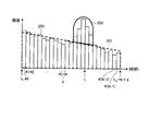
- FIG. 2 is a diagram showing an example of a histogram based on the time when the light receiving unit 3 is applicable, which is applicable to the embodiment of the present disclosure.
- the horizontal axis indicates the bin and the vertical axis indicates the frequency for each bin.
- the bins are obtained by classifying the light receiving time t m for each predetermined unit time d.
- bin # 0 is 0 ⁇ t m ⁇ d
- bin # 1 is d ⁇ t m ⁇ 2 ⁇ d
- bin # 2 is 2 ⁇ d ⁇ t m ⁇ 3 ⁇ d
- Bin # (N). -2) is (N-2) ⁇ d ⁇ t m ⁇ (N-1) ⁇ d.
- the distance measuring device 1 counts the number of times the light receiving time t m is acquired based on the bin, obtains the frequency 200 for each bin, and generates a histogram.
- the light receiving unit 3 also receives light other than the reflected light L2 from which the emitted light L1 emitted from the light source unit 2 is reflected.
- ambient light is light that is randomly incident on the light receiving unit 3, and the ambient light component 201 due to the ambient light in the histogram becomes noise for the target reflected light L2.
- the target reflected light L2 is light received according to a specific distance and appears as an active light component 202 in the histogram.
- the bin corresponding to the frequency of the peak in the active light component 202 is the bin corresponding to the distance D of the object to be measured 100.
- the distance measuring device 1 acquires the representative time of the bottle (for example, the time in the center of the bottle) as the time t 1 described above, and calculates the distance D to the object to be measured 100 according to the above formula (1). be able to. As described above, by using a plurality of light reception results, it is possible to perform appropriate distance measurement for random noise.
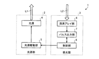
- FIG. 3 is a block diagram showing a configuration example of the distance measuring device 1 according to the embodiment of the present disclosure.
- the distance measuring device 1 includes a light source unit 2 and a light receiving unit 3.
- the light source unit 2 has a light source 4 and a light source driving unit 5.
- the light source 4 is composed of, for example, a laser diode such as a vertical cavity surface emitting laser (VCSEL: Vertical Cavity Surface Emitting LASER).
- VCSEL Vertical Cavity Surface Emitting LASER
- the light source 4 is not limited to the VCSEL, and a laser diode array in which laser diodes are arranged on a line may be used.
- the light source driving unit 5 drives the light source 4.
- the light source driving unit 5 drives the light source 4 so that the light source 4 emits the emitted light L1 having a predetermined timing and a pulse width based on a light emission control signal from the control unit 8 of the light receiving unit 3, for example.
- the light source driving unit 5 can drive the light source 4 so that the laser light is scanned in the direction perpendicular to the line, for example, from the light source 4 having the laser diodes arranged on the line.
- the light receiving unit 3 has a pixel array unit 6, a pulse output unit 7, and a control unit 8.
- the pixel array unit 6 has a plurality of SPAD elements 6a (see FIG. 4) arranged in a two-dimensional lattice pattern.
- SPAD element 6a when a large reverse bias voltage that causes an avalanche multiplier is applied to the cathode, the avalanche multiplier is internally generated due to the electrons generated in response to the incident of one photon.
- the SPAD element 6a has a characteristic that a large current flows according to the incident of one photon. Then, the SPAD element 6a can detect the incident of one photon contained in the reflected light L2 with high sensitivity by utilizing such a characteristic.
- the operation of the plurality of SPAD elements 6a in the pixel array unit 6 is controlled by the control unit 8.
- the control unit 8 may control the reading of the signal from each SPAD element 6a for each block including (n ⁇ m) SPAD elements 6a of n pixels in the row direction and m pixels in the column direction. it can.
- control unit 8 can read the signal from each SPAD element 6a by scanning each SPAD element 6a in the row direction and by scanning each row in the column direction in units of the block.
- control unit 8 may independently read a signal from each SPAD element 6a.
- the signal generated by the SPAD element 6a of the pixel array unit 6 is supplied to the pulse output unit 7.
- the pulse output unit 7 outputs a predetermined pulse signal as a digital signal to the control unit 8 in response to the signal generated by the SPAD element 6a.
- the details of the pulse output unit 7 will be described later.
- the control unit 8 controls the overall operation of the distance measuring device 1 according to a program incorporated in advance, for example.
- the control unit 8 controls the light emission timing of the light source 4 by controlling the light source driving unit 5.
- control unit 8 generates the histogram shown in FIG. 2 based on the pulse signal output from the pulse output unit 7. Further, the control unit 8 performs a predetermined calculation process based on the generated histogram data to calculate the distance D to the DUT 100.
- FIG. 4 is a schematic diagram showing an example of a device configuration applicable to the light receiving unit 3 according to the embodiment of the present disclosure.
- the light receiving unit 3 is configured by laminating a light receiving chip 3a made of a semiconductor chip and a logic chip 3b, respectively.
- the light receiving chip 3a and the logic chip 3b are shown in a separated state for easy understanding.
- the SPAD elements 6a are arranged in a two-dimensional lattice pattern in the region of the pixel array unit 6.
- the logic chip 3b is provided with a pulse output unit 7 and a control unit 8.
- the configuration of the light receiving chip 3a and the logic chip 3b is not limited to the example of FIG.
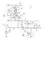
- FIG. 5 is a circuit diagram showing a configuration example of the pulse output unit 7 according to the embodiment of the present disclosure.
- the pulse output unit 7 includes a first wiring 10, a second wiring 11, a current supply unit 20, an enable unit 30, a first withstand voltage unit 40, and a second withstand voltage.
- a unit 50 and an inverter 60 are provided.
- the enable unit 30 has a first enable unit 31 and a second enable unit 32.
- the first power supply voltage Vdd1 is applied to the first wiring 10.
- the first power supply voltage Vdd1 is a voltage (for example, 5V) higher than the withstand voltage (for example, 3.3V) of various transistors constituting the pulse output unit 7.
- a second power supply voltage Vdd2 is applied to the second wiring 11.
- the second power supply voltage Vdd2 is a voltage (for example, 2.5V) lower than the withstand voltage of the first power supply voltage Vdd1 and the various transistors constituting the pulse output unit 7.
- the first power supply voltage Vdd1 and the second power supply voltage Vdd2 are not limited to the above examples, and the first power supply voltage Vdd1 is a value higher than the withstand voltage of various transistors, and the second power supply voltage Vdd2 is If the value is lower than the withstand voltage of various transistors, it can be adjusted as appropriate.
- first power supply voltage Vdd1 and the second power supply voltage Vdd2 can be appropriately adjusted as long as the potential difference between the first power supply voltage Vdd1 and the second power supply voltage Vdd2 is lower than the withstand voltage of various transistors. Is.
- the current supply unit 20 supplies a predetermined current from the first wiring 10 to the SPAD element 6a.
- the current supply unit 20 has a P-type transistor 21 and a P-type transistor 22 connected in series.
- the P-type transistor 21 is an example of a third transistor.
- the source of the P-type transistor 21 is connected to the first wiring 10
- the drain of the P-type transistor 21 is connected to the source of the P-type transistor 22
- the gate of the P-type transistor 21 is connected to the second wiring 11. Further, the substrate potential of the P-type transistor 21 is the same potential as the drain of the P-type transistor 21.
- the source of the P-type transistor 22 is connected to the drain of the P-type transistor 21.
- the drain of the P-type transistor 22 is connected to the source of the P-type transistor 33 included in the first enable unit 31 of the enable unit 30.
- the substrate potential of the P-type transistor 22 is the same potential as the source of the P-type transistor 22.
- control unit 8 inputs a predetermined reference voltage V REF to the gate of the P-type transistor 22.
- the current supply unit 20 SPADs a predetermined current controlled by the reference voltage V REF via the first enable unit 31 of the enable unit 30, the first withstand voltage unit 40, and the signal line 12. It is supplied to the cathode of the element 6a.
- the signal line 12 is connected between the cathode of the SPAD element 6a and the input terminal of the inverter 60 via the connection portion 6b of the pixel array portion 6 and the N-type transistor 51 of the second withstand voltage portion 50. Further, the anode of the SPAD element 6a is grounded, and the output terminal of the inverter 60 is connected to the control unit 8 (see FIG. 3) via the node 13.
- the enable unit 30 executes and stops the operation of the SPAD element 6a based on the enable signal sent from the outside (for example, the control unit 8).
- the upper channel P-type transistor 33 and the lower channel N-type transistor 34 form a CMOS circuit.
- the first enable unit 31 executes and stops the operation of the SPAD element 6a by inputting the first enable signal E1 which is a part of the enable signal to the CMOS circuit.
- the P-type transistor 33 becomes conductive, so that the node 35, which is the output unit of the CMOS circuit, is the current supply unit. Connected to 20.
- a predetermined current can be supplied from the current supply unit 20 to the SPAD element 6a, so that the first enable unit 31 can operate the SPAD element 6a.
- the P-type transistor 33 functions as a part of the current supply unit 20.
- the N-type transistor 34 becomes conductive, so that the node 35, which is the output unit of the CMOS circuit, is second. Is connected to the wiring 11. That is, the node 35 is held at the second power supply voltage Vdd2.
- the supply of current from the current supply unit 20 to the SPAD element 6a can be stopped, so that the first enable unit 31 can stop the operation of the SPAD element 6a.
- the details of the second enable unit 32 will be described later.
- the first withstand voltage unit 40 holds the low voltage side (that is, the node 35) of the current supply unit 20 at a voltage equal to or higher than the second power supply voltage Vdd2.
- the first pressure-resistant portion 40 has a P-type transistor 41.
- the source of the P-type transistor 41 is connected to the node 35.
- the drain of the P-type transistor 41 is connected to the SPAD element 6a side of the N-type transistor 51 on the signal line 12.
- the substrate potential of the P-type transistor 41 is the same potential as the source of the P-type transistor 41.
- the P-type transistor 41 can hold the voltage of the node 35 at a voltage equal to or higher than the second power supply voltage Vdd2. That is, the first withstand voltage unit 40 can hold the node 35 at a voltage equal to or higher than the second power supply voltage Vdd2.
- the second withstand voltage section 50 holds the inverter 60 at a voltage equal to or lower than the second power supply voltage Vdd2.
- the second pressure-resistant portion 50 includes an N-type transistor 51 and a P-type transistor 52.
- the N-type transistor 51 is an example of the first transistor
- the P-type transistor 52 is an example of the second transistor.
- the drain of the N-type transistor 51 is connected to the cathode of the SPAD element 6a via the connection portion 6b of the pixel array portion 6.
- the source of the N-type transistor 51 is connected to the input terminal of the inverter 60.
- the substrate potential of the N-type transistor 51 is the same potential as the source of the N-type transistor 51.
- the second withstand voltage unit 50 can hold the inverter 60 at a voltage equal to or lower than the second power supply voltage Vdd2.
- the source of the P-type transistor 52 is connected to the second wiring 11.
- the source of the P-type transistor 52 is connected to the source of the N-type transistor 51 via the signal line 12.
- the gate of the P-type transistor 52 is connected to the output terminal of the inverter 60 via the node 13. The function of the P-type transistor 52 will be described later.
- the second enable unit 32 of the enable unit 30 has an N-type transistor 36.
- the drain of the N-type transistor 36 is connected to the inverter 60 side of the N-type transistor 51 on the signal line 12.
- the source of the N-type transistor 36 is grounded.
- the second enable unit 32 executes and stops the operation of the SPAD element 6a by inputting the second enable signal E2, which is a part of the enable signal, to the gate of the N-type transistor 36.
- the N-type transistor 36 is disconnected, so that the signal from the SPAD element 6a can be input to the inverter 60.
- the second enable unit 32 can reflect the operation of the SPAD element 6a on the output of the pulse output unit 7.
- the N-type transistor 36 becomes conductive, so that the cathode of the SPAD element 6a can be clamped to the ground potential. it can. As a result, a large reverse bias voltage is not applied to the cathode of the SPAD element 6a, so that the second enable unit 32 can prevent the SPAD element 6a from operating.
- FIG. 6 is an explanatory diagram showing the operation of the pulse output unit 7 when the SPAD element 6a is operated in the embodiment of the present disclosure with a timing chart.
- the first enable signal E1 having the same voltage as the second power supply voltage Vdd2 is input to the first enable unit 31. Further, a second enable signal E2, which is a ground voltage, is input to the second enable unit 32.
- a reverse bias first power supply voltage Vdd1 is applied to the SPAD element 6a until a state called Geiger mode, which is on the verge of avalanche amplification, is reached. That is, in the initial state, the signal S1 output from the cathode of the SPAD element 6a becomes the first power supply voltage Vdd1.
- the signal S2 output from the current supply unit 20 via the node 35 becomes the first power supply voltage Vdd1 like the signal S1.
- the drain voltage of the N-type transistor 51 is the first power supply voltage Vdd1
- the gate voltage of the N-type transistor 51 is the first.
- the power supply voltage of 2 is Vdd2. Therefore, when the signal S1 is the first power supply voltage Vdd1, the N-type transistor 51 is in a disconnected state.
- the low level signal S4 is input to the gate of the P-type transistor 52. Then, the P-type transistor 52 becomes conductive.
- the voltage between the source of the N-type transistor 51 and the input terminal of the inverter 60 (hereinafter, also referred to as signal S3) becomes the second power supply voltage Vdd2. Since the second power supply voltage Vdd2 having a threshold voltage Vth or higher is input to the inverter 60 as the signal S3, the signal S4 output from the inverter 60 remains at a low level.
- the first power supply voltage Vdd1 is applied to the drain of the N-type transistor 51, and the second power supply voltage Vdd2 is applied to the source of the N-type transistor 51.
- the pulse output unit 7 feeds back the output of the inverter 60 to the P-type transistor 52, so that the second source of the N-type transistor 51 is in the initial state, that is, when the signal S1 is the first power supply voltage Vdd1. Power supply voltage Vdd2 can be applied.
- the N-type transistor 51 has a withstand voltage lower than that of the first power supply voltage Vdd1, it is possible to prevent the N-type transistor 51 from being damaged.
- the SPAD element 6a breaks down and a current is supplied from the current supply unit 20.
- the signal S1 sharply decreases from the first power supply voltage Vdd1.
- the signal S2 sharply decreases from the first power supply voltage Vdd1 together with the signal S1.
- the signal S2 stops lowering at a voltage Va larger than the second power supply voltage Vdd2 at the time T2. This is because the second power supply voltage Vdd2 is applied to the gate of the P-type transistor 41.
- this voltage Va is a value obtained by adding the threshold voltage of the P-type transistor 41 to the second power supply voltage Vdd2, and is a voltage lower than the withstand voltage of various transistors (for example, the P-type transistor 41).
- the current supply unit 20 is formed of various transistors having a withstand voltage lower than that of the first power supply voltage Vdd1, it is possible to prevent the various transistors from being damaged.
- the drain-gate voltage of the N-type transistor 51 becomes zero, so that the N-type transistor 51 becomes conductive.
- the signal S3 sharply decreases from the second power supply voltage Vdd2 together with the signal S1.
- the inverter 60 outputs a high level (for example, the second power supply voltage Vdd2) signal S4.
- the signals S1 and S3 stop lowering at zero (V). Further, the signal S1 and the signal S3 are raised by recharging the SPAD element 6a via the current supply unit 20 (so-called quenching operation).
- the voltage Va is applied to the source of the P-type transistor 41, and the drain of the P-type transistor 41 is zero (V).
- the applied voltage Va is lower than the withstand voltage of the P-type transistor 41, in the embodiment, even if the signal S1 or the like becomes zero (V), the P-type transistor 41 is prevented from being damaged. can do.
- the high-level signal S4 is input to the gate of the P-type transistor 52, so that the P-type transistor 52 is in a disconnected state.
- the inverter 60 outputs the low-level signal S4.
- the P-type transistor 52 becomes conductive, so that a current is supplied to the SPAD element 6a via the P-type transistor 52 and the N-type transistor 51. Therefore, the signal S1 and the signal S3 rise sharply.
- the drain-gate voltage of the N-type transistor 51 becomes larger than zero, so that the N-type transistor 51 is in a disconnected state.
- the signal S3 stays high at the second power supply voltage Vdd2 at the time T6, and is held at the second power supply voltage Vdd2 after the time T6.
- the P-type transistor 52 or the inverter 60 is formed by various transistors having a withstand voltage lower than the first power supply voltage Vdd1, it is possible to prevent the P-type transistor 52 or the inverter 60 from being damaged. can do.
- the signal S1 and the signal S2 (that is, the cathode of the SPAD element 6a) return to the first power supply voltage Vdd1 in the initial state at time T8, and the SPAD element 6a and the pulse output unit 7 return to the initial state.
- the pulse output unit 7 can apply the first power supply voltage Vdd1 which is a voltage higher than the withstand voltage of various transistors to the cathode of the SPAD element 6a. Therefore, according to the embodiment, the sensitivity characteristic of the SPAD element 6a can be improved.
- the second power supply voltage Vdd1 is supplied to the first wiring 10 before the first power supply voltage Vdd1 is supplied.
- a second power supply voltage Vdd2 is supplied to the wiring 11.
- the second power supply voltage Vdd2 is supplied before the first power supply voltage Vdd1 is supplied, the second power supply voltage Vdd2 is applied to the drain of the P-type transistor 22 in the current supply unit 20. Will be done.
- the parasitic diode formed between the drain of the P-type transistor 22 and the substrate is turned on, so that a current may flow in the P-type transistor 22.
- the P-type transistor 21 in which the substrate potential and the drain have the same potential is provided in the current supply unit 20 in series with the P-type transistor 22. Since the drain and the substrate potential of the P-type transistor 21 are the same potential, the internal parasitic diode does not turn on even if the second power supply voltage Vdd2 is applied to the drain.
- the current supply unit 20 is filled with power. It is possible to suppress the flow of electric current.
- FIG. 7 is an explanatory diagram showing the operation of the pulse output unit 7 when the operation of the SPAD element 6a is stopped in the embodiment of the present disclosure with a timing chart.
- the first enable signal E1 having the same voltage as the first power supply voltage Vdd1 is input to the first enable unit 31.
- the N-type transistor 34 becomes conductive, so that the node 35, which is the output unit of the CMOS circuit, is connected to the second wiring 11. Therefore, since the source and the gate of the P-type transistor 41 have the same potential, the P-type transistor 41 is in a disconnected state. As a result, the current supply from the current supply unit 20 to the SPAD element 6a can be stopped.
- the second enable signal E2 having the same voltage as the second power supply voltage Vdd2 is input to the second enable unit 32.
- the N-type transistor 51 is clamped to the ground potential, and the N-type transistor 51 is in a conductive state, so that the cathode of the SPAD element 6a is also clamped to the ground potential.
- the inverter 60 outputs a high level (for example, the second power supply voltage Vdd2) signal S4.
- the SPAD element is input by inputting the predetermined first enable signal E1 to the first enable unit 31 and inputting the predetermined second enable signal E2 to the second enable unit 32.
- the operation of 6a can be stopped.
- another first enable signal E1 is input to the first enable unit 31, and another second enable signal E2 is input to the second enable unit 32.
- the SPAD element 6a By inputting, the SPAD element 6a can be operated.
- the operation of the SPAD element 6a can be performed and stopped by switching between the first enable signal E1 and the second enable signal E2.
- the pulse output unit 7 sends a high-level signal S4 to the control unit 8, but the control unit 8 turns off the high-level signal S4. It should be processed as.
- the control circuit includes a first wiring 10, a second wiring 11, a current supply unit 20, a first pressure-resistant unit 40, an inverter 60, and a second pressure-resistant unit 50.
- a first power supply voltage Vdd1 is applied to the first wiring 10.
- a second power supply voltage Vdd2 lower than the first power supply voltage Vdd1 is applied to the second wiring 11.
- the current supply unit 20 supplies a predetermined current from the first wiring 10 to the SPAD element 6a.
- the first withstand voltage unit 40 holds the low voltage side of the current supply unit 20 at a voltage equal to or higher than the second power supply voltage Vdd2.
- the inverter 60 is connected to the cathode of the SPAD element 6a.
- the second withstand voltage section 50 holds the inverter 60 at a voltage equal to or lower than the second power supply voltage Vdd2. Further, the second withstand voltage portion 50 includes an N-type first transistor (N-type transistor 51) and a P-type second transistor (P-type transistor 52).
- the N-type first transistor (N-type transistor 51) is provided between the cathode of the SPAD element 6a and the input terminal of the inverter 60, and the gate is connected to the second wiring 11.
- the P-type second transistor (P-type transistor 52) is provided between the second wiring 11 and the source of the first transistor (N-type transistor 51), and the gate is connected to the output terminal of the inverter 60.
- the first power supply voltage Vdd1 is higher than the withstand voltage of the first transistor (N-type transistor 51) and the second transistor (P-type transistor 52).
- the second power supply voltage Vdd2 is lower than the withstand voltage of the first transistor (N-type transistor 51) and the second transistor (P-type transistor 52).
- the potential difference between the first power supply voltage Vdd1 and the second power supply voltage Vdd2 is lower than the withstand voltage of the first transistor (N-type transistor 51) and the second transistor (P-type transistor 52).
- the current supply unit 20 is of a P type in which the source is connected to the first wiring 10, the gate is connected to the second wiring 11, and the drain is the same potential as the substrate potential. It has a third transistor (P-type transistor 21).
- control circuit further includes an enable unit 30 that executes and stops the operation of the SPAD element 6a based on the enable signal.
- the enable unit 30 has a first enable unit 31 and a second enable unit 32.
- the first enable unit 31 holds the low voltage side of the current supply unit 20 at the second power supply voltage Vdd2 based on the enable signal (first enable signal E1).
- the second enable unit 32 grounds the input terminal of the inverter 60 based on the enable signal (second enable signal E2).
- the current supply unit 20 is composed of the P-type transistor 21 and the P-type transistor 22 is shown, but when the current supply unit 20 is composed of the P-type transistor 21 and the P-type transistor 22 Not limited.
- the first enable unit 31 is composed of a CMOS circuit
- the case where the first enable unit 31 is composed of a CMOS circuit is not limited to the case.
- the second enable unit 32 is composed of the N-type transistor 36
- the case where the second enable unit 32 is composed of the N-type transistor 36 is not limited to the case.
- the first withstand voltage portion 40 is composed of the P-type transistor 41
- the first withstand voltage portion 40 is not limited to the case where the P-type transistor 41 is formed.
- the second withstand voltage portion 50 is composed of the N-type transistor 51 and the P-type transistor 52 is shown, but the second withstand voltage portion 50 is composed of the N-type transistor 51 and the P-type transistor 52. It is not limited to the case where it is done.
- the present technology can also have the following configurations.
- SPAD Single Photon Avalanche Diode
- a P-type second transistor provided between the second wiring and the source of the first transistor and having a gate connected to the output terminal of the inverter.
- Control circuit with. (2) The first power supply voltage is higher than the withstand voltage of the first transistor and the second transistor.
- the second power supply voltage is lower than the withstand voltage of the first transistor and the second transistor.
- the control circuit according to (1) wherein the potential difference between the first power supply voltage and the second power supply voltage is lower than the withstand voltage of the first transistor and the second transistor.
- the enable part is A first enable unit that holds the low voltage side of the current supply unit at the second power supply voltage based on the enable signal, and a first enable unit.
- a second enable unit that grounds the input terminal of the inverter based on the enable signal, and The control circuit according to any one of (1) to (3) above.
- a light source that irradiates the object to be measured with light, A SPAD element that outputs a signal when the light reflected from the object to be measured is received, and A first wiring to which a first power supply voltage is applied, a second wiring to which a second power supply voltage lower than the first power supply voltage is applied, and a predetermined wiring from the first wiring to the SPAD element.
- a current supply unit that supplies the current, a first withstand voltage unit that holds the low voltage side of the current supply unit at a voltage equal to or higher than the second power supply voltage, an inverter connected to the cathode of the SPAD element, and the above.
- a second withstand voltage portion that holds the inverter at a voltage equal to or lower than the second power supply voltage is provided, and the second withstand voltage portion is provided between the cathode of the SPAD element and the input terminal of the inverter.
- a gate is provided between the N-type first transistor connected to the second wiring and the source of the second wiring and the first transistor, and the gate is connected to the output terminal of the inverter.
- a control circuit having a second transistor of the type, Distance measuring system equipped with. (6)
- the first power supply voltage is higher than the withstand voltage of the first transistor and the second transistor.
- the second power supply voltage is lower than the withstand voltage of the first transistor and the second transistor.
- the distance measuring system according to (5), wherein the potential difference between the first power supply voltage and the second power supply voltage is lower than the withstand voltage of the first transistor and the second transistor.
- the control circuit further includes an enable unit that executes and stops the operation of the SPAD element based on the enable signal.
- the enable part is A first enable unit that holds the low voltage side of the current supply unit at the second power supply voltage based on the enable signal, and a first enable unit.
- a second enable unit that grounds the input terminal of the inverter based on the enable signal, and The distance measuring system according to any one of (5) to (7) above.
- Second wiring 20 Current supply unit 21 P-type transistor (an example of a third transistor) 30 Enable section 31 First enable section 32 Second enable section 40 First withstand voltage section 50 Second withstand voltage section 51 N-type transistor (an example of the first transistor) 52 P-type transistor (an example of a second transistor) 60 inverter
Landscapes
- Engineering & Computer Science (AREA)
- Physics & Mathematics (AREA)
- General Physics & Mathematics (AREA)
- Computer Networks & Wireless Communication (AREA)
- Radar, Positioning & Navigation (AREA)
- Remote Sensing (AREA)
- Electromagnetism (AREA)
- Signal Processing (AREA)
- Multimedia (AREA)
- Spectroscopy & Molecular Physics (AREA)
- Light Receiving Elements (AREA)
- Logic Circuits (AREA)
- Transforming Light Signals Into Electric Signals (AREA)
- Optical Radar Systems And Details Thereof (AREA)
- Photometry And Measurement Of Optical Pulse Characteristics (AREA)
Abstract
本開示に係る制御回路は、第1の電源電圧(Vdd1)が印加される第1の配線(10)と、第1の電源電圧(Vdd1)より低い第2の電源電圧(Vdd2)が印加される第2の配線(20)と、第1の配線(10)からSPAD素子(6a)に所定の電流を供給する電流供給部(20)と、電流供給部(20)の低圧側を第2の電源電圧(Vdd2)以上の電圧に保持する第1の耐圧部(40)と、SPAD素子(6a)のカソードに接続されるインバータ(60)と、インバータ(60)を第2の電源電圧(Vdd2)以下の電圧に保持しSPAD素子(6a)のカソードとインバータ(60)の入力端子との間に設けられゲートが第2の配線(11)に接続されるN型の第1トランジスタと第2の配線(11)と第1トランジスタのソースとの間に設けられゲートがインバータ(60)の出力端子に接続されるP型の第2トランジスタとを有する第2の耐圧部(50)とを備える。
Description
本開示は、制御回路および測距システムに関する。
光を用いて被測定物までの距離を測定する測距方式の一つとして、直接ToF(Time of Flight)方式と呼ばれる測距手法が知られている。かかる直接ToF方式では、光源から射出された光が被測定物により反射された反射光を受光素子により受光し、光が射出されてから反射光として受光されるまでの時間に基づき対象までの距離を計測する(たとえば、特許文献1参照)。
しかしながら、上記の従来技術では、受光素子として用いられるSPAD(Single Photon Avalanche Diode)素子の感度特性を向上させることは困難である。
そこで、本開示では、SPAD素子の感度特性を向上させることができる制御回路および測距システムを提案する。
本開示によれば、制御回路が提供される。制御回路は、第1の配線と、第2の配線と、電流供給部と、第1の耐圧部と、インバータと、第2の耐圧部とを備える。第1の配線には、第1の電源電圧が印加される。第2の配線には、前記第1の電源電圧よりも低い第2の電源電圧が印加される。電流供給部は、前記第1の配線からSPAD(Single Photon Avalanche Diode)素子に所定の電流を供給する。第1の耐圧部は、前記電流供給部の低圧側を前記第2の電源電圧以上の電圧に保持する。インバータは、前記SPAD素子のカソードに接続される。第2の耐圧部は、前記インバータを前記第2の電源電圧以下の電圧に保持する。また、前記第2の耐圧部は、N型の第1トランジスタと、P型の第2トランジスタとを有する。N型の第1トランジスタは、前記SPAD素子のカソードと前記インバータの入力端子との間に設けられ、ゲートが前記第2の配線に接続される。P型の第2トランジスタは、前記第2の配線と前記第1トランジスタのソースとの間に設けられ、ゲートが前記インバータの出力端子に接続される。
本開示によれば、SPAD素子の感度特性を向上させることができる。なお、ここに記載された効果は必ずしも限定されるものではなく、本開示中に記載されたいずれかの効果であってもよい。
以下に、本開示の各実施形態について図面に基づいて詳細に説明する。なお、以下の各実施形態において、同一の部位には同一の符号を付することにより重複する説明を省略する。
光を用いて被測定物までの距離を測定する測距方式の一つとして、直接ToF方式と呼ばれる測距手法が知られている。かかる直接ToF方式では、光源から射出された光が被測定物により反射された反射光を受光素子により受光し、光が射出されてから反射光として受光されるまでの時間に基づき対象までの距離を計測する。
しかしながら、上記の従来技術では、受光素子として用いられるSPAD素子の感度特性を向上させることは困難である。
なぜなら、SPAD素子の感度特性は、かかるSPAD素子のカソードに印加される電圧の値が高いほど向上する一方、印加回路を構成する各種トランジスタの耐電圧よりもSPAD素子のカソードに印加される電圧の値を高くすることは困難であるからである。
そこで、上述の問題点を克服し、SPAD素子の感度特性を向上させることができる制御回路および測距システムの実現が期待されている。
[測距方法]
本開示は、光を用いて測距を行う技術に関するものである。そこで、本開示の実施形態の理解を容易とするために、図1および図2を参照しながら、実施形態に適用可能な測距方法について説明する。
本開示は、光を用いて測距を行う技術に関するものである。そこで、本開示の実施形態の理解を容易とするために、図1および図2を参照しながら、実施形態に適用可能な測距方法について説明する。
図1は、本開示の実施形態に適用可能である直接ToF方式による測距を模式的に示す図である。実施形態では、測距方式として直接ToF方式を適用する。
かかる直接ToF方式は、光源部2からの射出光L1が被測定物100により反射した反射光L2を受光部3により受光し、光の射出タイミングと受光タイミングとの差分の時間に基づき測距を行う方式である。
測距装置1は、光源部2と、受光部3とを備える。測距装置1は、測距システムの一例である。光源部2は、たとえばレーザダイオードである光源4(図3参照)を有し、レーザ光をパルス状に発光するように駆動される。
光源部2からの射出光L1は、被測定物100により反射され、反射光L2として受光部3に受光される。受光部3は、光電変換によって光を電気信号に変換する画素アレイ部6(図3参照)を含み、受光した光に応じた信号を出力する。
ここで、光源部2が発光した時刻(発光タイミング)を時間t0、光源部2からの射出光L1が被測定物100により反射された反射光L2を受光部3が受光した時刻(受光タイミング)を時間t1とする。
定数cを光速度(2.9979×10⁸[m/sec])とすると、測距装置1と被測定物100との間の距離Dは、次式(1)により計算される。
D=(c/2)×(t1-t0) …(1)
D=(c/2)×(t1-t0) …(1)
なお、測距装置1は、上述の処理を、複数回繰り返して実行するとよい。また、受光部3は、複数のSPAD素子6a(図4参照)を有し、各SPAD素子6aに反射光L2が受光された各受光タイミングに基づき距離Dをそれぞれ算出してもよい。
測距装置1は、発光タイミングの時間t0から受光部3に光が受光された受光タイミングまでの時間tm(以下、「受光時間tm」とも呼称する。)を階級(ビン(bins))に基づき分類し、ヒストグラムを生成する。
図2は、本開示の実施形態に適用可能である受光部3が受光した時刻に基づく一例のヒストグラムを示す図である。図2において、横軸はビン、縦軸はビン毎の頻度を示す。ビンは、受光時間tmを所定の単位時間d毎に分類したものである。
具体的には、ビン#0が0≦tm<d、ビン#1がd≦tm<2×d、ビン#2が2×d≦tm<3×d、…、ビン#(N-2)が(N-2)×d≦tm<(N-1)×dとなる。受光部3の露光時間を時間tepとした場合、tep=N×dとなる。
測距装置1は、受光時間tmを取得した回数をビンに基づき計数してビン毎の頻度200を求め、ヒストグラムを生成する。ここで、受光部3は、光源部2からの射出光L1が反射された反射光L2以外の光も受光する。
たとえば、対象となる反射光L2以外の光の例として、測距装置1の周囲の環境光がある。かかる環境光は、受光部3にランダムに入射する光であって、ヒストグラムにおける環境光による環境光成分201は、対象となる反射光L2に対するノイズとなる。
一方、対象となる反射光L2は、特定の距離に応じて受光される光であって、ヒストグラムにおいてアクティブ光成分202として現れる。このアクティブ光成分202内のピークの頻度に対応するビンが、被測定物100の距離Dに対応するビンとなる。
測距装置1は、そのビンの代表時間(たとえばビンの中央の時間)を上述した時間t1として取得することで、上述した式(1)に従い、被測定物100までの距離Dを算出することができる。このように、複数の受光結果を用いることで、ランダムなノイズに対して適切な測距が実行可能となる。
[測距装置の構成]
つづいて、実施形態に係る測距装置1の構成について、図3および図4を参照しながら説明する。図3は、本開示の実施形態に係る測距装置1の構成例を示すブロック図である。上述のように、測距装置1は、光源部2と、受光部3とを備える。
つづいて、実施形態に係る測距装置1の構成について、図3および図4を参照しながら説明する。図3は、本開示の実施形態に係る測距装置1の構成例を示すブロック図である。上述のように、測距装置1は、光源部2と、受光部3とを備える。
光源部2は、光源4と、光源駆動部5とを有する。光源4は、たとえば、垂直共振器面発光レーザ(VCSEL:Vertical Cavity Surface Emitting LASER)などのレーザダイオードで構成される。なお、光源4は、VCSELに限られず、レーザダイオードがライン上に配列されたレーザダイオードアレイなどを用いてもよい。
光源駆動部5は、光源4を駆動する。光源駆動部5は、たとえば、受光部3の制御部8からの発光制御信号に基づき、光源4から所定のタイミングおよびパルス幅を有する射出光L1が出射されるように光源4を駆動する。
光源駆動部5は、たとえば、ライン上に配列されるレーザダイオードを有する光源4から、レーザ光がラインに垂直の方向にスキャンされるように光源4を駆動することができる。
受光部3は、画素アレイ部6と、パルス出力部7と、制御部8とを有する。
画素アレイ部6は、2次元格子状に配列される複数のSPAD素子6a(図4参照)を有する。かかるSPAD素子6aは、アバランシ増倍が発生する大きな逆バイアス電圧をカソードに印加することにより、1光子の入射に応じて発生した電子に起因して、内部でアバランシ増倍が生じる。
すなわち、SPAD素子6aは、1光子の入射に応じて大電流が流れる特性を有する。そして、SPAD素子6aでは、かかる特性を利用することで、反射光L2に含まれる1光子の入射を高感度で検知することができる。
画素アレイ部6における複数のSPAD素子6aの動作は、制御部8によって制御される。たとえば、制御部8は、各SPAD素子6aからの信号の読み出しを、行方向にn画素、列方向にm画素の、(n×m)個のSPAD素子6aを含むブロック毎に制御することができる。
また、制御部8は、当該ブロックを単位として、各SPAD素子6aを行方向にスキャンし、さらに行毎に列方向にスキャンして、各SPAD素子6aから信号を読み出すことができる。
なお、実施形態において、制御部8は、各SPAD素子6aからそれぞれ単独に信号を読み出してもよい。画素アレイ部6のSPAD素子6aで発生する信号は、パルス出力部7に供給される。
パルス出力部7は、SPAD素子6aで発生する信号に応じて、所定のパルス信号をデジタル信号として制御部8に出力する。かかるパルス出力部7の詳細については後述する。
制御部8は、たとえば予め組み込まれるプログラムに従い、測距装置1の全体の動作を制御する。たとえば、制御部8は、光源駆動部5を制御することにより、光源4の発光タイミングを制御する。
また、制御部8は、パルス出力部7から出力されるパルス信号に基づいて、図2に示したヒストグラムを生成する。また、制御部8は、生成されたヒストグラムのデータに基づいて所定の演算処理を行い、被測定物100までの距離Dを算出する。
図4は、本開示の実施形態に係る受光部3に適用可能であるデバイスの構成の例を示す模式図である。図4において、受光部3は、それぞれ半導体チップからなる受光チップ3aとロジックチップ3bとが積層されて構成される。なお、図4では、理解の容易のため、受光チップ3aとロジックチップ3bとが分離された状態で示している。
受光チップ3aには、画素アレイ部6の領域にSPAD素子6aが2次元格子状に配列される。ロジックチップ3bには、パルス出力部7と、制御部8とが設けられる。なお、受光チップ3aおよびロジックチップ3bの構成は、図4の例に限定されない。
[パルス出力部の構成および動作]
つづいて、実施形態に係るパルス出力部7の構成および動作について、図5~図7を参照しながら説明する。図5は、本開示の実施形態に係るパルス出力部7の構成例を示す回路図である。
つづいて、実施形態に係るパルス出力部7の構成および動作について、図5~図7を参照しながら説明する。図5は、本開示の実施形態に係るパルス出力部7の構成例を示す回路図である。
図5に示すように、パルス出力部7は、第1の配線10と、第2の配線11と、電流供給部20と、イネーブル部30と、第1の耐圧部40と、第2の耐圧部50と、インバータ60とを備える。また、イネーブル部30は、第1のイネーブル部31と、第2のイネーブル部32とを有する。
第1の配線10には、第1の電源電圧Vdd1が印加される。かかる第1の電源電圧Vdd1は、パルス出力部7を構成する各種トランジスタの耐電圧(たとえば、3.3V)よりも高い電圧(たとえば、5V)である。
第2の配線11には、第2の電源電圧Vdd2が印加される。かかる第2の電源電圧Vdd2は、第1の電源電圧Vdd1およびパルス出力部7を構成する各種トランジスタの耐電圧よりも低い電圧(たとえば、2.5V)である。
なお、第1の電源電圧Vdd1および第2の電源電圧Vdd2は、上述の例に限られず、第1の電源電圧Vdd1が各種トランジスタの耐電圧よりも高い値であり、第2の電源電圧Vdd2が各種トランジスタの耐電圧よりも低い値であれば、適宜調整可能である。
さらに、第1の電源電圧Vdd1および第2の電源電圧Vdd2は、第1の電源電圧Vdd1と第2の電源電圧Vdd2との電位差が各種トランジスタの耐電圧よりも低い値であれば、適宜調整可能である。
電流供給部20は、第1の配線10からSPAD素子6aに所定の電流を供給する。電流供給部20は、直列に接続されるP型トランジスタ21およびP型トランジスタ22を有する。P型トランジスタ21は、第3のトランジスタの一例である。
P型トランジスタ21のソースは第1の配線10に接続され、P型トランジスタ21のドレインはP型トランジスタ22のソースに接続され、P型トランジスタ21のゲートは第2の配線11に接続される。また、P型トランジスタ21の基板電位は、P型トランジスタ21のドレインと同電位である。
P型トランジスタ22のソースはP型トランジスタ21のドレインに接続される。P型トランジスタ22のドレインは、イネーブル部30の第1のイネーブル部31に含まれるP型トランジスタ33のソースに接続される。P型トランジスタ22の基板電位は、P型トランジスタ22のソースと同電位である。
また、制御部8は、P型トランジスタ22のゲートに所定のリファレンス電圧VREFを入力する。これにより、電流供給部20は、イネーブル部30の第1のイネーブル部31と、第1の耐圧部40と、信号線12とを介して、リファレンス電圧VREFで制御された所定の電流をSPAD素子6aのカソードに供給する。
なお、信号線12は、画素アレイ部6の接続部6bおよび第2の耐圧部50のN型トランジスタ51を介して、SPAD素子6aのカソードとインバータ60の入力端子との間を接続する。また、SPAD素子6aのアノードは接地され、インバータ60の出力端子はノード13を介して制御部8(図3参照)に接続される。
イネーブル部30は、外部(たとえば、制御部8)から送られるイネーブル信号に基づいて、SPAD素子6aの動作の実施および停止を行う。イネーブル部30の第1のイネーブル部31は、上チャネルのP型トランジスタ33と、下チャネルのN型トランジスタ34とがCMOS回路となって構成される。
そして、第1のイネーブル部31は、かかるCMOS回路にイネーブル信号の一部である第1のイネーブル信号E1が入力されることにより、SPAD素子6aの動作の実施および停止を行う。
たとえば、第2の電源電圧Vdd2と同じ電圧の第1のイネーブル信号E1が入力されることにより、P型トランジスタ33が導通状態となることから、CMOS回路の出力部であるノード35が電流供給部20に接続される。
これにより、電流供給部20からSPAD素子6aに所定の電流を供給することができることから、第1のイネーブル部31は、SPAD素子6aを動作させることができる。そしてこの場合、P型トランジスタ33は、電流供給部20の一部として機能する。
一方で、第1の電源電圧Vdd1と同じ電圧の第1のイネーブル信号E1が入力されることにより、N型トランジスタ34が導通状態となることから、CMOS回路の出力部であるノード35が第2の配線11に接続される。すなわち、ノード35は、第2の電源電圧Vdd2で保持される。
これにより、電流供給部20からSPAD素子6aへの電流の供給を停止することができることから、第1のイネーブル部31は、SPAD素子6aの動作を停止させることができる。なお、第2のイネーブル部32の詳細については後述する。
第1の耐圧部40は、電流供給部20の低圧側(すなわち、ノード35)を第2の電源電圧Vdd2以上の電圧に保持する。第1の耐圧部40は、P型トランジスタ41を有する。
P型トランジスタ41のソースは、ノード35に接続される。P型トランジスタ41のドレインは、信号線12においてN型トランジスタ51よりもSPAD素子6a側に接続される。P型トランジスタ41の基板電位は、P型トランジスタ41のソースと同電位である。
また、P型トランジスタ41のゲートは第2の配線11に接続されることから、P型トランジスタ41は、ノード35の電圧を第2の電源電圧Vdd2以上の電圧に保持することができる。すなわち、第1の耐圧部40は、ノード35を第2の電源電圧Vdd2以上の電圧に保持することができる。
第2の耐圧部50は、インバータ60を第2の電源電圧Vdd2以下の電圧に保持する。第2の耐圧部50は、N型トランジスタ51と、P型トランジスタ52とを有する。N型トランジスタ51は、第1のトランジスタの一例であり、P型トランジスタ52は、第2のトランジスタの一例である。
N型トランジスタ51のドレインは、画素アレイ部6の接続部6bを介してSPAD素子6aのカソードに接続される。N型トランジスタ51のソースは、インバータ60の入力端子に接続される。N型トランジスタ51の基板電位は、N型トランジスタ51のソースと同電位である。
また、N型トランジスタ51のゲートは第2の配線11に接続されることから、インバータ60の電圧が第2の電源電圧Vdd2よりも大きくなる場合、N型トランジスタ51は切断状態となる。これにより、第2の耐圧部50は、インバータ60を第2の電源電圧Vdd2以下の電圧に保持することができる。
P型トランジスタ52のソースは、第2の配線11に接続される。P型トランジスタ52のソースは、信号線12を介してN型トランジスタ51のソースに接続される。P型トランジスタ52のゲートは、ノード13を介してインバータ60の出力端子に接続される。かかるP型トランジスタ52の機能については後述する。
イネーブル部30の第2のイネーブル部32は、N型トランジスタ36を有する。N型トランジスタ36のドレインは、信号線12においてN型トランジスタ51よりもインバータ60側に接続される。N型トランジスタ36のソースは接地される。
そして、第2のイネーブル部32は、N型トランジスタ36のゲートにイネーブル信号の一部である第2のイネーブル信号E2が入力されることにより、SPAD素子6aの動作の実施および停止を行う。
たとえば、グランド電圧である第2のイネーブル信号E2が入力されることにより、N型トランジスタ36が切断状態となることから、SPAD素子6aからの信号をインバータ60に入力させることができる。これにより、第2のイネーブル部32は、SPAD素子6aの動作をパルス出力部7の出力に反映させることができる。
また、第2の電源電圧Vdd2と同じ電圧の第2のイネーブル信号E2が入力されることにより、N型トランジスタ36が導通状態となることから、SPAD素子6aのカソードを接地電位にクランプすることができる。これにより、SPAD素子6aのカソードに大きな逆バイアス電圧が印加されなくなることから、第2のイネーブル部32は、SPAD素子6aを動作させないことができる。
次に、図5に加えて図6も参照しながら、パルス出力部7の動作について説明する。図6は、本開示の実施形態においてSPAD素子6aを動作させている場合のパルス出力部7の動作をタイミングチャートで示す説明図である。
SPAD素子6aを動作させる場合、上述のように、第1のイネーブル部31には、第2の電源電圧Vdd2と同じ電圧の第1のイネーブル信号E1が入力される。また、第2のイネーブル部32には、グランド電圧である第2のイネーブル信号E2が入力される。
パルス出力部7の初期状態において、SPAD素子6aには、ガイガーモードと呼ばれるなだれ増幅が起きる寸前の状態になるまで、逆バイアスの第1の電源電圧Vdd1が印加されている。すなわち、初期状態において、SPAD素子6aのカソードから出力される信号S1は、この第1の電源電圧Vdd1となる。
また、パルス出力部7の初期状態において、電流供給部20からノード35を介して出力される信号S2は、信号S1と同じく第1の電源電圧Vdd1となる。
また、SPAD素子6aのカソードから出力される信号S1が第1の電源電圧Vdd1である場合、N型トランジスタ51のドレイン電圧は第1の電源電圧Vdd1であり、N型トランジスタ51のゲート電圧は第2の電源電圧Vdd2である。したがって、信号S1が第1の電源電圧Vdd1である場合、N型トランジスタ51は切断状態となる。
そして、パルス出力部7の初期状態では、インバータ60から出力される信号S4がローレベル(たとえば、ゼロ(V))であることから、かかるローレベルの信号S4がP型トランジスタ52のゲートに入力され、P型トランジスタ52は導通状態となる。
これにより、N型トランジスタ51のソースとインバータ60の入力端子との間の電圧(以下、信号S3とも呼称する。)は、第2の電源電圧Vdd2となる。なお、インバータ60にはしきい電圧Vth以上の第2の電源電圧Vdd2が信号S3として入力されることから、インバータ60から出力される信号S4はローレベルのままである。
このように、パルス出力部7の初期状態では、N型トランジスタ51のドレインに第1の電源電圧Vdd1が印加され、N型トランジスタ51のソースに第2の電源電圧Vdd2が印加される。
すなわち、パルス出力部7は、インバータ60の出力をP型トランジスタ52にフィードバックさせることにより、初期状態、即ち信号S1が第1の電源電圧Vdd1である場合に、N型トランジスタ51のソースに第2の電源電圧Vdd2を印加することができる。
したがって、実施形態によれば、第1の電源電圧Vdd1よりも耐電圧が低いN型トランジスタ51であっても、かかるN型トランジスタ51が破損することを抑制することができる。
そして、第1の電源電圧Vdd1が印加されたSPAD素子6aに時間T1で1光子が入射すると、SPAD素子6aがブレイクダウンして電流供給部20から電流が供給される。これにより、信号S1は、第1の電源電圧Vdd1から急激に減少する。
同様に、信号S2は、信号S1とともに第1の電源電圧Vdd1から急激に減少する。一方で、信号S2は、時間T2において、第2の電源電圧Vdd2よりも大きい電圧Vaで下げ止まる。これは、P型トランジスタ41のゲートに第2の電源電圧Vdd2が印加されているためである。
なお、この電圧Vaは、第2の電源電圧Vdd2にP型トランジスタ41のしきい値電圧を加えた値であり、各種トランジスタ(たとえば、P型トランジスタ41)の耐電圧よりも低い電圧である。
このように、信号S2が第2の電源電圧Vdd2より低くなることを防止することにより、電流供給部20を形成する各種トランジスタのソース-ドレイン間に、耐電圧よりも大きい電位差が生じることを抑制することができる。
したがって、実施形態によれば、第1の電源電圧Vdd1よりも耐電圧が低い各種トランジスタで電流供給部20を形成した場合でも、かかる各種トランジスタが破損することを抑制することができる。
そして、信号S1が第2の電源電圧Vdd2になると、N型トランジスタ51のドレイン-ゲート間電圧がゼロになることから、N型トランジスタ51が導通状態となる。これにより、信号S3は、第2の電源電圧Vdd2から信号S1とともに急激に減少する。
そして、時間T3で信号S3がしきい電圧Vthより小さくなると、インバータ60はハイレベル(たとえば、第2の電源電圧Vdd2)の信号S4を出力する。
そして、信号S1および信号S3は、時間T4でSPAD素子6a内のなだれ増幅が停止することから、ゼロ(V)で下げ止まる。さらに、信号S1および信号S3は、電流供給部20を介してSPAD素子6aが再充電されることにより上昇する(いわゆるクエンチング動作)。
また、信号S1および信号S3がゼロ(V)で下げ止まった時間T4において、P型トランジスタ41のソースには電圧Vaが印加され、P型トランジスタ41のドレインはゼロ(V)である。
しかしながら、かかる電圧VaはP型トランジスタ41の耐電圧よりも低い電圧であることから、実施形態では、信号S1などがゼロ(V)になった場合でも、P型トランジスタ41が破損することを抑制することができる。
また、インバータ60からハイレベルの信号S4が出力された時間T3において、かかるハイレベルの信号S4がP型トランジスタ52のゲートに入力されることから、P型トランジスタ52は切断状態となる。
これにより、第2の配線11からP型トランジスタ52およびN型トランジスタ51を介してSPAD素子6aが再充電されることを抑制することができる。したがって、実施形態によれば、電流供給部20以外の供給路からSPAD素子6aに電流が供給されることにより、SPAD素子6aの動作が不安定になることを抑制することができる。
そして、信号S3がしきい電圧Vth以上になった時間T5で、インバータ60はローレベルの信号S4を出力する。これにより、P型トランジスタ52が導通状態となることから、かかるP型トランジスタ52およびN型トランジスタ51を介して電流がSPAD素子6aに供給される。したがって、信号S1および信号S3は急激に上昇する。
しかしながら、信号S1が第2の電源電圧Vdd2より大きくなると、N型トランジスタ51のドレイン-ゲート間電圧がゼロより大きくなることから、N型トランジスタ51が切断状態となる。これにより、信号S3は、時間T6において第2の電源電圧Vdd2で高止まり、時間T6以降は第2の電源電圧Vdd2で保持される。
これにより、P型トランジスタ52やインバータ60に対して、第2の電源電圧Vdd2よりも大きい電圧が印加されることを抑制することができる。
したがって、実施形態によれば、第1の電源電圧Vdd1よりも耐電圧が低い各種トランジスタでP型トランジスタ52やインバータ60を形成した場合でも、かかるP型トランジスタ52やインバータ60が破損することを抑制することができる。
そして、信号S1がさらに上昇し、ノード35が電圧Va以上になった時間T7以降は、信号S2が信号S1とともに上昇する。最後に、信号S1および信号S2(すなわち、SPAD素子6aのカソード)は、時間T8で初期状態の第1の電源電圧Vdd1に復帰し、SPAD素子6aおよびパルス出力部7は初期状態に戻る。
ここまで説明したように、実施形態に係るパルス出力部7は、SPAD素子6aのカソードに各種トランジスタの耐電圧よりも高い電圧である第1の電源電圧Vdd1を印加することができる。したがって、実施形態によれば、SPAD素子6aの感度特性を向上させることができる。
また、実施形態では、上述のように、パルス出力部7を構成する各トランジスタに対して、SPAD素子6aのすべての動作段階で耐電圧よりも大きい電位差が生じることを抑制することができる。
したがって、実施形態によれば、耐電圧よりも高い第1の電源電圧Vdd1を用いた場合でも、パルス出力部7を構成する各トランジスタが破損することを抑制することができる。
なお、実施形態に係るパルス出力部7に電源を投入する際には、各種トランジスタの耐圧を確保するため、第1の配線10に第1の電源電圧Vdd1を供給するよりも先に、第2の配線11に第2の電源電圧Vdd2を供給する。
一方で、第1の電源電圧Vdd1を供給するよりも先に第2の電源電圧Vdd2を供給した場合、電流供給部20内のP型トランジスタ22のドレインには、第2の電源電圧Vdd2が印加される。
これにより、かかるP型トランジスタ22のドレインと基板との間に形成される寄生ダイオードがオンすることから、P型トランジスタ22内に電流が流れる恐れがある。
そこで、実施形態では、基板電位とドレインとが同電位であるP型トランジスタ21を、P型トランジスタ22と直列に電流供給部20内に設けることとした。かかるP型トランジスタ21は、ドレインと基板電位とが同電位であることから、ドレインに第2の電源電圧Vdd2が印加されたとしても、内部の寄生ダイオードがオンすることはない。
すなわち、実施形態によれば、基板電位とドレインとが同電位であるP型トランジスタ21を電流供給部20に設けることにより、パルス出力部7に電源を投入する際に、電流供給部20内に電流が流れることを抑制することができる。
図7は、本開示の実施形態においてSPAD素子6aの動作を停止させた場合のパルス出力部7の動作をタイミングチャートで示す説明図である。
SPAD素子6aの動作を停止させる場合、第1のイネーブル部31には、第1の電源電圧Vdd1と同じ電圧の第1のイネーブル信号E1が入力される。
これにより、N型トランジスタ34が導通状態となることから、CMOS回路の出力部であるノード35が第2の配線11に接続される。したがって、P型トランジスタ41のソースとゲートとが同電位になることから、P型トランジスタ41は切断状態となる。これにより、電流供給部20からSPAD素子6aへの電流供給を停止することができる。
また、SPAD素子6aの動作を停止させる場合、第2のイネーブル部32には、第2の電源電圧Vdd2と同じ電圧の第2のイネーブル信号E2が入力される。
これにより、N型トランジスタ51が接地電位にクランプされ、N型トランジスタ51が導通状態となることから、SPAD素子6aのカソードも接地電位にクランプされる。
このように、SPAD素子6aの動作を停止させた場合、図7に示すように、初期状態において、信号S1および信号S3が接地電位にクランプされ、信号S2が第2の電源電圧Vdd2で保持される。したがって、インバータ60からは、ハイレベル(たとえば、第2の電源電圧Vdd2)の信号S4が出力される。
さらに、SPAD素子6aの動作を停止させた場合、時間T10でSPAD素子6aに1光子が入射した場合でも、大きな逆バイアス電圧がカソードに印加されていないことから、SPAD素子6aの内部ではアバランシ増倍が生じない。
このように、実施形態では、第1のイネーブル部31に所定の第1のイネーブル信号E1を入力し、第2のイネーブル部32に所定の第2のイネーブル信号E2を入力することにより、SPAD素子6aの動作を停止させることができる。
一方で、実施形態では、図6に示したように、第1のイネーブル部31に別の第1のイネーブル信号E1を入力し、第2のイネーブル部32に別の第2のイネーブル信号E2を入力することにより、SPAD素子6aを動作させることができる。
すなわち、実施形態によれば、第1のイネーブル信号E1および第2のイネーブル信号E2を切り替えることにより、SPAD素子6aの動作の実施および停止を行うことができる。
なお、実施形態においてSPAD素子6aの動作を停止させた場合、パルス出力部7からはハイレベルの信号S4が制御部8に送られるが、制御部8は、かかるハイレベルの信号S4をオフ信号として処理するとよい。
[効果]
実施形態に係る制御回路は、第1の配線10と、第2の配線11と、電流供給部20と、第1の耐圧部40と、インバータ60と、第2の耐圧部50とを備える。第1の配線10には、第1の電源電圧Vdd1が印加される。第2の配線11には、第1の電源電圧Vdd1よりも低い第2の電源電圧Vdd2が印加される。電流供給部20は、第1の配線10からSPAD素子6aに所定の電流を供給する。第1の耐圧部40は、電流供給部20の低圧側を第2の電源電圧Vdd2以上の電圧に保持する。インバータ60は、SPAD素子6aのカソードに接続される。第2の耐圧部50は、インバータ60を第2の電源電圧Vdd2以下の電圧に保持する。また、第2の耐圧部50は、N型の第1トランジスタ(N型トランジスタ51)と、P型の第2トランジスタ(P型トランジスタ52)とを有する。N型の第1トランジスタ(N型トランジスタ51)は、SPAD素子6aのカソードとインバータ60の入力端子との間に設けられ、ゲートが第2の配線11に接続される。P型の第2トランジスタ(P型トランジスタ52)は、第2の配線11と第1トランジスタ(N型トランジスタ51)のソースとの間に設けられ、ゲートがインバータ60の出力端子に接続される。
実施形態に係る制御回路は、第1の配線10と、第2の配線11と、電流供給部20と、第1の耐圧部40と、インバータ60と、第2の耐圧部50とを備える。第1の配線10には、第1の電源電圧Vdd1が印加される。第2の配線11には、第1の電源電圧Vdd1よりも低い第2の電源電圧Vdd2が印加される。電流供給部20は、第1の配線10からSPAD素子6aに所定の電流を供給する。第1の耐圧部40は、電流供給部20の低圧側を第2の電源電圧Vdd2以上の電圧に保持する。インバータ60は、SPAD素子6aのカソードに接続される。第2の耐圧部50は、インバータ60を第2の電源電圧Vdd2以下の電圧に保持する。また、第2の耐圧部50は、N型の第1トランジスタ(N型トランジスタ51)と、P型の第2トランジスタ(P型トランジスタ52)とを有する。N型の第1トランジスタ(N型トランジスタ51)は、SPAD素子6aのカソードとインバータ60の入力端子との間に設けられ、ゲートが第2の配線11に接続される。P型の第2トランジスタ(P型トランジスタ52)は、第2の配線11と第1トランジスタ(N型トランジスタ51)のソースとの間に設けられ、ゲートがインバータ60の出力端子に接続される。
これにより、SPAD素子6aの感度特性を向上させることができる。
また、実施形態に係る制御回路において、第1の電源電圧Vdd1は、第1トランジスタ(N型トランジスタ51)および第2トランジスタ(P型トランジスタ52)の耐電圧よりも高い。また、第2の電源電圧Vdd2は、第1トランジスタ(N型トランジスタ51)および第2トランジスタ(P型トランジスタ52)の耐電圧よりも低い。また、第1の電源電圧Vdd1と第2の電源電圧Vdd2との電位差は、第1トランジスタ(N型トランジスタ51)および第2トランジスタ(P型トランジスタ52)の耐電圧よりも低い。
これにより、耐電圧よりも高い第1の電源電圧Vdd1を用いた場合でも、パルス出力部7を構成する各トランジスタが破損することを抑制することができる。
また、実施形態に係る制御回路において、電流供給部20は、ソースが第1の配線10に接続され、ゲートが第2の配線11に接続され、ドレインが基板電位と同電位であるP型の第3トランジスタ(P型トランジスタ21)を有する。
これにより、パルス出力部7に電源を投入する際に、電流供給部20内に電流が流れることを抑制することができる。
また、実施形態に係る制御回路は、イネーブル信号に基づいてSPAD素子6aの動作の実施および停止を行うイネーブル部30をさらに備える。イネーブル部30は、第1のイネーブル部31と第2のイネーブル部32とを有する。第1のイネーブル部31は、イネーブル信号(第1のイネーブル信号E1)に基づいて電流供給部20の低圧側を第2の電源電圧Vdd2に保持する。第2のイネーブル部32は、イネーブル信号(第2のイネーブル信号E2)に基づいてインバータ60の入力端子を接地する。
これにより、SPAD素子6aの動作を停止させることができる。
以上、本開示の実施形態について説明したが、本開示の技術的範囲は、上述の実施形態そのままに限定されるものではなく、本開示の要旨を逸脱しない範囲において種々の変更が可能である。また、異なる実施形態及び変形例にわたる構成要素を適宜組み合わせてもよい。
たとえば、実施形態では、電流供給部20がP型トランジスタ21およびP型トランジスタ22で構成された例について示したが、電流供給部20はP型トランジスタ21およびP型トランジスタ22で構成される場合に限られない。
また、実施形態では、第1のイネーブル部31がCMOS回路で構成された例について示したが、第1のイネーブル部31はCMOS回路で構成される場合に限られない。
また、実施形態では、第2のイネーブル部32がN型トランジスタ36で構成された例について示したが、第2のイネーブル部32はN型トランジスタ36で構成される場合に限られない。
また、実施形態では、第1の耐圧部40がP型トランジスタ41で構成された例について示したが、第1の耐圧部40はP型トランジスタ41で構成される場合に限られない。
また、実施形態では、第2の耐圧部50がN型トランジスタ51およびP型トランジスタ52で構成された例について示したが、第2の耐圧部50はN型トランジスタ51およびP型トランジスタ52で構成される場合に限られない。
また、本明細書に記載された効果はあくまで例示であって限定されるものでは無く、また他の効果があってもよい。
なお、本技術は以下のような構成も取ることができる。
(1)
第1の電源電圧が印加される第1の配線と、
前記第1の電源電圧よりも低い第2の電源電圧が印加される第2の配線と、
前記第1の配線からSPAD(Single Photon Avalanche Diode)素子に所定の電流を供給する電流供給部と、
前記電流供給部の低圧側を前記第2の電源電圧以上の電圧に保持する第1の耐圧部と、
前記SPAD素子のカソードに接続されるインバータと、
前記インバータを前記第2の電源電圧以下の電圧に保持する第2の耐圧部と、
を備え、
前記第2の耐圧部は、
前記SPAD素子のカソードと前記インバータの入力端子との間に設けられ、ゲートが前記第2の配線に接続されるN型の第1トランジスタと、
前記第2の配線と前記第1トランジスタのソースとの間に設けられ、ゲートが前記インバータの出力端子に接続されるP型の第2トランジスタと、
を有する制御回路。
(2)
前記第1の電源電圧は、前記第1トランジスタおよび前記第2トランジスタの耐電圧よりも高く、
前記第2の電源電圧は、前記第1トランジスタおよび前記第2トランジスタの耐電圧よりも低く、
前記第1の電源電圧と前記第2の電源電圧との電位差は、前記第1トランジスタおよび前記第2トランジスタの耐電圧よりも低い
前記(1)に記載の制御回路。
(3)
前記電流供給部は、
ソースが前記第1の配線に接続され、ゲートが前記第2の配線に接続され、ドレインが基板電位と同電位であるP型の第3トランジスタを有する
前記(1)または(2)に記載の制御回路。
(4)
イネーブル信号に基づいてSPAD素子の動作の実施および停止を行うイネーブル部をさらに備え、
前記イネーブル部は、
前記イネーブル信号に基づいて前記電流供給部の低圧側を前記第2の電源電圧に保持する第1のイネーブル部と、
前記イネーブル信号に基づいて前記インバータの入力端子を接地する第2のイネーブル部と、
を有する前記(1)~(3)のいずれか一つに記載の制御回路。
(5)
被測定物に光を照射する光源と、
前記被測定物から反射される光を受光した際に信号を出力するSPAD素子と、
第1の電源電圧が印加される第1の配線と、前記第1の電源電圧よりも低い第2の電源電圧が印加される第2の配線と、前記第1の配線から前記SPAD素子に所定の電流を供給する電流供給部と、前記電流供給部の低圧側を前記第2の電源電圧以上の電圧に保持する第1の耐圧部と、前記SPAD素子のカソードに接続されるインバータと、前記インバータを前記第2の電源電圧以下の電圧に保持する第2の耐圧部と、を備え、前記第2の耐圧部は、前記SPAD素子のカソードと前記インバータの入力端子との間に設けられ、ゲートが前記第2の配線に接続されるN型の第1トランジスタと、前記第2の配線と前記第1トランジスタのソースとの間に設けられ、ゲートが前記インバータの出力端子に接続されるP型の第2トランジスタと、を有する制御回路と、
を備える測距システム。
(6)
前記第1の電源電圧は、前記第1トランジスタおよび前記第2トランジスタの耐電圧よりも高く、
前記第2の電源電圧は、前記第1トランジスタおよび前記第2トランジスタの耐電圧よりも低く、
前記第1の電源電圧と前記第2の電源電圧との電位差は、前記第1トランジスタおよび前記第2トランジスタの耐電圧よりも低い
前記(5)に記載の測距システム。
(7)
前記電流供給部は、
ソースが前記第1の配線に接続され、ゲートが前記第2の配線に接続され、ドレインが基板電位と同電位であるP型の第3トランジスタを有する
前記(5)または(6)に記載の測距システム。
(8)
前記制御回路は、イネーブル信号に基づいてSPAD素子の動作の実施および停止を行うイネーブル部をさらに備え、
前記イネーブル部は、
前記イネーブル信号に基づいて前記電流供給部の低圧側を前記第2の電源電圧に保持する第1のイネーブル部と、
前記イネーブル信号に基づいて前記インバータの入力端子を接地する第2のイネーブル部と、
を有する前記(5)~(7)のいずれか一つに記載の測距システム。
(1)
第1の電源電圧が印加される第1の配線と、
前記第1の電源電圧よりも低い第2の電源電圧が印加される第2の配線と、
前記第1の配線からSPAD(Single Photon Avalanche Diode)素子に所定の電流を供給する電流供給部と、
前記電流供給部の低圧側を前記第2の電源電圧以上の電圧に保持する第1の耐圧部と、
前記SPAD素子のカソードに接続されるインバータと、
前記インバータを前記第2の電源電圧以下の電圧に保持する第2の耐圧部と、
を備え、
前記第2の耐圧部は、
前記SPAD素子のカソードと前記インバータの入力端子との間に設けられ、ゲートが前記第2の配線に接続されるN型の第1トランジスタと、
前記第2の配線と前記第1トランジスタのソースとの間に設けられ、ゲートが前記インバータの出力端子に接続されるP型の第2トランジスタと、
を有する制御回路。
(2)
前記第1の電源電圧は、前記第1トランジスタおよび前記第2トランジスタの耐電圧よりも高く、
前記第2の電源電圧は、前記第1トランジスタおよび前記第2トランジスタの耐電圧よりも低く、
前記第1の電源電圧と前記第2の電源電圧との電位差は、前記第1トランジスタおよび前記第2トランジスタの耐電圧よりも低い
前記(1)に記載の制御回路。
(3)
前記電流供給部は、
ソースが前記第1の配線に接続され、ゲートが前記第2の配線に接続され、ドレインが基板電位と同電位であるP型の第3トランジスタを有する
前記(1)または(2)に記載の制御回路。
(4)
イネーブル信号に基づいてSPAD素子の動作の実施および停止を行うイネーブル部をさらに備え、
前記イネーブル部は、
前記イネーブル信号に基づいて前記電流供給部の低圧側を前記第2の電源電圧に保持する第1のイネーブル部と、
前記イネーブル信号に基づいて前記インバータの入力端子を接地する第2のイネーブル部と、
を有する前記(1)~(3)のいずれか一つに記載の制御回路。
(5)
被測定物に光を照射する光源と、
前記被測定物から反射される光を受光した際に信号を出力するSPAD素子と、
第1の電源電圧が印加される第1の配線と、前記第1の電源電圧よりも低い第2の電源電圧が印加される第2の配線と、前記第1の配線から前記SPAD素子に所定の電流を供給する電流供給部と、前記電流供給部の低圧側を前記第2の電源電圧以上の電圧に保持する第1の耐圧部と、前記SPAD素子のカソードに接続されるインバータと、前記インバータを前記第2の電源電圧以下の電圧に保持する第2の耐圧部と、を備え、前記第2の耐圧部は、前記SPAD素子のカソードと前記インバータの入力端子との間に設けられ、ゲートが前記第2の配線に接続されるN型の第1トランジスタと、前記第2の配線と前記第1トランジスタのソースとの間に設けられ、ゲートが前記インバータの出力端子に接続されるP型の第2トランジスタと、を有する制御回路と、
を備える測距システム。
(6)
前記第1の電源電圧は、前記第1トランジスタおよび前記第2トランジスタの耐電圧よりも高く、
前記第2の電源電圧は、前記第1トランジスタおよび前記第2トランジスタの耐電圧よりも低く、
前記第1の電源電圧と前記第2の電源電圧との電位差は、前記第1トランジスタおよび前記第2トランジスタの耐電圧よりも低い
前記(5)に記載の測距システム。
(7)
前記電流供給部は、
ソースが前記第1の配線に接続され、ゲートが前記第2の配線に接続され、ドレインが基板電位と同電位であるP型の第3トランジスタを有する
前記(5)または(6)に記載の測距システム。
(8)
前記制御回路は、イネーブル信号に基づいてSPAD素子の動作の実施および停止を行うイネーブル部をさらに備え、
前記イネーブル部は、
前記イネーブル信号に基づいて前記電流供給部の低圧側を前記第2の電源電圧に保持する第1のイネーブル部と、
前記イネーブル信号に基づいて前記インバータの入力端子を接地する第2のイネーブル部と、
を有する前記(5)~(7)のいずれか一つに記載の測距システム。
1 測距装置(測距システムの一例)
2 光源部
3 受光部
6a SPAD素子
7 パルス出力部
8 制御部
10 第1の配線
11 第2の配線
20 電流供給部
21 P型トランジスタ(第3のトランジスタの一例)
30 イネーブル部
31 第1のイネーブル部
32 第2のイネーブル部
40 第1の耐圧部
50 第2の耐圧部
51 N型トランジスタ(第1のトランジスタの一例)
52 P型トランジスタ(第2のトランジスタの一例)
60 インバータ
2 光源部
3 受光部
6a SPAD素子
7 パルス出力部
8 制御部
10 第1の配線
11 第2の配線
20 電流供給部
21 P型トランジスタ(第3のトランジスタの一例)
30 イネーブル部
31 第1のイネーブル部
32 第2のイネーブル部
40 第1の耐圧部
50 第2の耐圧部
51 N型トランジスタ(第1のトランジスタの一例)
52 P型トランジスタ(第2のトランジスタの一例)
60 インバータ
Claims (5)
- 第1の電源電圧が印加される第1の配線と、
前記第1の電源電圧よりも低い第2の電源電圧が印加される第2の配線と、
前記第1の配線からSPAD(Single Photon Avalanche Diode)素子に所定の電流を供給する電流供給部と、
前記電流供給部の低圧側を前記第2の電源電圧以上の電圧に保持する第1の耐圧部と、
前記SPAD素子のカソードに接続されるインバータと、
前記インバータを前記第2の電源電圧以下の電圧に保持する第2の耐圧部と、
を備え、
前記第2の耐圧部は、
前記SPAD素子のカソードと前記インバータの入力端子との間に設けられ、ゲートが前記第2の配線に接続されるN型の第1トランジスタと、
前記第2の配線と前記第1トランジスタのソースとの間に設けられ、ゲートが前記インバータの出力端子に接続されるP型の第2トランジスタと、
を有する制御回路。 - 前記第1の電源電圧は、前記第1トランジスタおよび前記第2トランジスタの耐電圧よりも高く、
前記第2の電源電圧は、前記第1トランジスタおよび前記第2トランジスタの耐電圧よりも低く、
前記第1の電源電圧と前記第2の電源電圧との電位差は、前記第1トランジスタおよび前記第2トランジスタの耐電圧よりも低い
請求項1に記載の制御回路。 - 前記電流供給部は、
ソースが前記第1の配線に接続され、ゲートが前記第2の配線に接続され、ドレインが基板電位と同電位であるP型の第3トランジスタを有する
請求項1に記載の制御回路。 - イネーブル信号に基づいてSPAD素子の動作の実施および停止を行うイネーブル部をさらに備え、
前記イネーブル部は、
前記イネーブル信号に基づいて前記電流供給部の低圧側を前記第2の電源電圧に保持する第1のイネーブル部と、
前記イネーブル信号に基づいて前記インバータの入力端子を接地する第2のイネーブル部と、
を有する請求項1に記載の制御回路。 - 被測定物に光を照射する光源と、
前記被測定物から反射される光を受光した際に信号を出力するSPAD素子と、
第1の電源電圧が印加される第1の配線と、前記第1の電源電圧よりも低い第2の電源電圧が印加される第2の配線と、前記第1の配線から前記SPAD素子に所定の電流を供給する電流供給部と、前記電流供給部の低圧側を前記第2の電源電圧以上の電圧に保持する第1の耐圧部と、前記SPAD素子のカソードに接続されるインバータと、前記インバータを前記第2の電源電圧以下の電圧に保持する第2の耐圧部と、を備え、前記第2の耐圧部は、前記SPAD素子のカソードと前記インバータの入力端子との間に設けられ、ゲートが前記第2の配線に接続されるN型の第1トランジスタと、前記第2の配線と前記第1トランジスタのソースとの間に設けられ、ゲートが前記インバータの出力端子に接続されるP型の第2トランジスタと、を有する制御回路と、
を備える測距システム。
Priority Applications (1)
| Application Number | Priority Date | Filing Date | Title |
|---|---|---|---|
| US17/310,815 US12392895B2 (en) | 2019-03-12 | 2019-12-17 | Control circuit and distance measurement system to improve sensitivity characteristics of SPAD element |
Applications Claiming Priority (2)
| Application Number | Priority Date | Filing Date | Title |
|---|---|---|---|
| JP2019-044809 | 2019-03-12 | ||
| JP2019044809A JP2020148537A (ja) | 2019-03-12 | 2019-03-12 | 制御回路および測距システム |
Publications (1)
| Publication Number | Publication Date |
|---|---|
| WO2020183843A1 true WO2020183843A1 (ja) | 2020-09-17 |
Family
ID=72427957
Family Applications (1)
| Application Number | Title | Priority Date | Filing Date |
|---|---|---|---|
| PCT/JP2019/049482 Ceased WO2020183843A1 (ja) | 2019-03-12 | 2019-12-17 | 制御回路および測距システム |
Country Status (3)
| Country | Link |
|---|---|
| US (1) | US12392895B2 (ja) |
| JP (1) | JP2020148537A (ja) |
| WO (1) | WO2020183843A1 (ja) |
Cited By (2)
| Publication number | Priority date | Publication date | Assignee | Title |
|---|---|---|---|---|
| US20220163642A1 (en) * | 2019-03-18 | 2022-05-26 | C/O Sony Semiconductor Solutions Corporation | Current generation circuit and ranging system |
| EP4300135A4 (en) * | 2021-02-25 | 2024-07-24 | Sony Semiconductor Solutions Corporation | LIGHT DETECTION DEVICE AND LIGHT DETECTION SYSTEM |
Families Citing this family (1)
| Publication number | Priority date | Publication date | Assignee | Title |
|---|---|---|---|---|
| US12571887B2 (en) | 2021-02-02 | 2026-03-10 | Sony Semiconductor Solutions Corporation | Light detection device, and distance measuring system |
Citations (6)
| Publication number | Priority date | Publication date | Assignee | Title |
|---|---|---|---|---|
| JPH02500789A (ja) * | 1986-11-25 | 1990-03-15 | イギリス国 | アバランシェフォトダイオードのケンチング回路 |
| JP2010219661A (ja) * | 2009-03-13 | 2010-09-30 | Fuji Electric Systems Co Ltd | 半導体装置 |
| JP2015117970A (ja) * | 2013-12-17 | 2015-06-25 | 株式会社デンソー | レーダ装置 |
| JP2018157387A (ja) * | 2017-03-17 | 2018-10-04 | キヤノン株式会社 | 撮像装置及び撮像システム |
| JP2019007877A (ja) * | 2017-06-27 | 2019-01-17 | キヤノン株式会社 | 光検出装置及び撮像システム |
| WO2019031001A1 (ja) * | 2017-08-09 | 2019-02-14 | ソニーセミコンダクタソリューションズ株式会社 | 固体撮像装置、電子装置および固体撮像装置の制御方法 |
Family Cites Families (3)
| Publication number | Priority date | Publication date | Assignee | Title |
|---|---|---|---|---|
| JP6225411B2 (ja) | 2012-10-16 | 2017-11-08 | 株式会社豊田中央研究所 | 光学的測距装置 |
| US9935618B1 (en) * | 2016-09-30 | 2018-04-03 | Tower Semiconductor Ltd. | Schmitt trigger circuit with hysteresis determined by modified polysilicon gate dopants |
| JP2019134230A (ja) * | 2018-01-29 | 2019-08-08 | ソニーセミコンダクタソリューションズ株式会社 | Dac回路、固体撮像素子、および、電子機器 |
-
2019
- 2019-03-12 JP JP2019044809A patent/JP2020148537A/ja active Pending
- 2019-12-17 US US17/310,815 patent/US12392895B2/en active Active
- 2019-12-17 WO PCT/JP2019/049482 patent/WO2020183843A1/ja not_active Ceased
Patent Citations (6)
| Publication number | Priority date | Publication date | Assignee | Title |
|---|---|---|---|---|
| JPH02500789A (ja) * | 1986-11-25 | 1990-03-15 | イギリス国 | アバランシェフォトダイオードのケンチング回路 |
| JP2010219661A (ja) * | 2009-03-13 | 2010-09-30 | Fuji Electric Systems Co Ltd | 半導体装置 |
| JP2015117970A (ja) * | 2013-12-17 | 2015-06-25 | 株式会社デンソー | レーダ装置 |
| JP2018157387A (ja) * | 2017-03-17 | 2018-10-04 | キヤノン株式会社 | 撮像装置及び撮像システム |
| JP2019007877A (ja) * | 2017-06-27 | 2019-01-17 | キヤノン株式会社 | 光検出装置及び撮像システム |
| WO2019031001A1 (ja) * | 2017-08-09 | 2019-02-14 | ソニーセミコンダクタソリューションズ株式会社 | 固体撮像装置、電子装置および固体撮像装置の制御方法 |
Cited By (3)
| Publication number | Priority date | Publication date | Assignee | Title |
|---|---|---|---|---|
| US20220163642A1 (en) * | 2019-03-18 | 2022-05-26 | C/O Sony Semiconductor Solutions Corporation | Current generation circuit and ranging system |
| EP4300135A4 (en) * | 2021-02-25 | 2024-07-24 | Sony Semiconductor Solutions Corporation | LIGHT DETECTION DEVICE AND LIGHT DETECTION SYSTEM |
| US12117313B2 (en) | 2021-02-25 | 2024-10-15 | Sony Semiconductor Solutions Corporation | Photodetection device and photodetection system |
Also Published As
| Publication number | Publication date |
|---|---|
| JP2020148537A (ja) | 2020-09-17 |
| US20220120898A1 (en) | 2022-04-21 |
| US12392895B2 (en) | 2025-08-19 |
Similar Documents
| Publication | Publication Date | Title |
|---|---|---|
| US12477840B2 (en) | Control circuit and distance measuring system | |
| US11913831B2 (en) | Optical sensor and method of operating an optical sensor | |
| US20120248514A1 (en) | Solid-state image sensing device | |
| US12405379B2 (en) | Time measurement apparatus | |
| CN211979200U (zh) | 传感器 | |
| US12007481B2 (en) | Sensor and distance measuring device | |
| US20220082668A1 (en) | Light detector and distance measurement device | |
| WO2020183843A1 (ja) | 制御回路および測距システム | |
| US12468018B2 (en) | Light detector and distance measuring device | |
| US11265500B2 (en) | Photodetection apparatus, electronic apparatus and photodetection method | |
| US11822014B2 (en) | Apparatus and method for controlling system timing within a LIDAR system | |
| US20220163642A1 (en) | Current generation circuit and ranging system | |
| US20250110220A1 (en) | Distance measurement device and equipment | |
| US20250386114A1 (en) | Range image generation device and equipment | |
| US20250123372A1 (en) | Image sensing device | |
| WO2020183842A1 (ja) | 制御回路および測距システム |
Legal Events
| Date | Code | Title | Description |
|---|---|---|---|
| 121 | Ep: the epo has been informed by wipo that ep was designated in this application |
Ref document number: 19918528 Country of ref document: EP Kind code of ref document: A1 |
|
| NENP | Non-entry into the national phase |
Ref country code: DE |
|
| 122 | Ep: pct application non-entry in european phase |
Ref document number: 19918528 Country of ref document: EP Kind code of ref document: A1 |
|
| WWG | Wipo information: grant in national office |
Ref document number: 17310815 Country of ref document: US |