WO2020183552A1 - 蒸着装置、および表示装置の製造方法 - Google Patents
蒸着装置、および表示装置の製造方法 Download PDFInfo
- Publication number
- WO2020183552A1 WO2020183552A1 PCT/JP2019/009531 JP2019009531W WO2020183552A1 WO 2020183552 A1 WO2020183552 A1 WO 2020183552A1 JP 2019009531 W JP2019009531 W JP 2019009531W WO 2020183552 A1 WO2020183552 A1 WO 2020183552A1
- Authority
- WO
- WIPO (PCT)
- Prior art keywords
- substrate
- vapor deposition
- mask
- alignment
- touch plate
- Prior art date
- Legal status (The legal status is an assumption and is not a legal conclusion. Google has not performed a legal analysis and makes no representation as to the accuracy of the status listed.)
- Ceased
Links
Images










Classifications
-
- C—CHEMISTRY; METALLURGY
- C23—COATING METALLIC MATERIAL; COATING MATERIAL WITH METALLIC MATERIAL; CHEMICAL SURFACE TREATMENT; DIFFUSION TREATMENT OF METALLIC MATERIAL; COATING BY VACUUM EVAPORATION, BY SPUTTERING, BY ION IMPLANTATION OR BY CHEMICAL VAPOUR DEPOSITION, IN GENERAL; INHIBITING CORROSION OF METALLIC MATERIAL OR INCRUSTATION IN GENERAL
- C23C—COATING METALLIC MATERIAL; COATING MATERIAL WITH METALLIC MATERIAL; SURFACE TREATMENT OF METALLIC MATERIAL BY DIFFUSION INTO THE SURFACE, BY CHEMICAL CONVERSION OR SUBSTITUTION; COATING BY VACUUM EVAPORATION, BY SPUTTERING, BY ION IMPLANTATION OR BY CHEMICAL VAPOUR DEPOSITION, IN GENERAL
- C23C14/00—Coating by vacuum evaporation, by sputtering or by ion implantation of the coating forming material
- C23C14/22—Coating by vacuum evaporation, by sputtering or by ion implantation of the coating forming material characterised by the process of coating
- C23C14/24—Vacuum evaporation
-
- C—CHEMISTRY; METALLURGY
- C23—COATING METALLIC MATERIAL; COATING MATERIAL WITH METALLIC MATERIAL; CHEMICAL SURFACE TREATMENT; DIFFUSION TREATMENT OF METALLIC MATERIAL; COATING BY VACUUM EVAPORATION, BY SPUTTERING, BY ION IMPLANTATION OR BY CHEMICAL VAPOUR DEPOSITION, IN GENERAL; INHIBITING CORROSION OF METALLIC MATERIAL OR INCRUSTATION IN GENERAL
- C23C—COATING METALLIC MATERIAL; COATING MATERIAL WITH METALLIC MATERIAL; SURFACE TREATMENT OF METALLIC MATERIAL BY DIFFUSION INTO THE SURFACE, BY CHEMICAL CONVERSION OR SUBSTITUTION; COATING BY VACUUM EVAPORATION, BY SPUTTERING, BY ION IMPLANTATION OR BY CHEMICAL VAPOUR DEPOSITION, IN GENERAL
- C23C14/00—Coating by vacuum evaporation, by sputtering or by ion implantation of the coating forming material
- C23C14/22—Coating by vacuum evaporation, by sputtering or by ion implantation of the coating forming material characterised by the process of coating
- C23C14/50—Substrate holders
Definitions
- the present invention relates to a method for manufacturing a vapor deposition apparatus and a display apparatus.
- Patent Documents 1 and 2 disclose a vapor deposition apparatus in which a substrate is arranged between a vapor deposition mask and a magnet, and the vapor deposition mask adheres to the substrate by the magnetic force of the magnet.
- the substrate alignment marks provided on both ends of the substrate, which are the objects to be deposited, and the mask alignment provided on the thin-film deposition mask are known that the alignment position confirmation for confirming whether or not the mark is within a predetermined allowable range is performed before the vapor deposition process is performed.
- the alignment position can not be confirmed efficiently, and there is a problem that the vapor deposition process and the manufacturing time of the display device cannot be shortened. ..
- the central portion of the substrate is first placed on the vapor deposition mask in a state of being bent by the weight of the substrate. After that, in the conventional thin-film deposition apparatus, the substrate is gradually placed on the vapor deposition mask in the direction from the center to both ends of the substrate, and after the entire surface of the substrate comes into contact with the vapor deposition mask, the alignment position is confirmed. It was done. For this reason, in the conventional thin-film deposition apparatus, when the alignment position is confirmed, the substrate alignment marks provided at both ends may be significantly deviated from the mask alignment marks due to the bending of the central portion.
- the present invention has been made in view of the above problems, and an object of the present invention is to realize a vapor deposition device and a method for manufacturing a display device, which can shorten the manufacturing time of the display device.
- the thin-film deposition apparatus is arranged between a thin-film deposition source, a thin-film deposition mask having a mask sheet and a mask frame, a magnet for bringing the mask sheet into close contact with the substrate, and the substrate and the magnet.
- a vapor deposition apparatus including a touch plate to be provided, an elevating device for raising and lowering the substrate with respect to the vapor deposition mask, and an alignment device for aligning the vapor deposition mask with the substrate.
- a plurality of support members that are provided around the substrate and that come into contact with a non-deposited region other than the surface to be vapor-deposited of the substrate to support the substrate, and the plurality of support members that are connected to the plurality of support members.
- the support members are provided with a drive mechanism that drives the support members in the elevating direction of the substrate independently of each other, and the drive mechanism is such that only one end of the substrate is pressed by the touch plate. While driving the support member so as to abut against the vapor deposition mask and pressing the substrate with the touch plate, the other end gradually moves toward the other end of the substrate and the other end becomes the vapor deposition mask. It is a configuration that drives the support member so as to abut.
- the method for manufacturing a display device is a method for manufacturing a display device having a substrate, which comprises a vapor deposition step of performing a vapor deposition process on the substrate by using a vapor deposition mask.
- a second driving step of driving the support member so that the other end of the substrate abuts on the vapor deposition mask gradually toward the other end of the substrate while pressing the substrate is included. , The method.
- FIG. 5 is a cross-sectional view taken along the longitudinal direction of the substrate which schematically shows a part of the vapor deposition process shown in FIG. FIG.
- FIG. 5 is another cross-sectional view along the longitudinal direction of the substrate, schematically showing a part of the vapor deposition process shown in FIG.
- FIG. 5 is another cross-sectional view along the longitudinal direction of the substrate, schematically showing a part of the vapor deposition process shown in FIG.
- FIG. 5 is another cross-sectional view along the longitudinal direction of the substrate, schematically showing a part of the vapor deposition process shown in FIG.
- FIG. 5 is another cross-sectional view along the longitudinal direction of the substrate, schematically showing a part of the vapor deposition process shown in FIG.
- FIG. 5 is another cross-sectional view along the longitudinal direction of the substrate, schematically showing a part of the vapor deposition process shown in FIG.
- FIG. 1 It is sectional drawing along the longitudinal direction of a substrate which shows an example of the schematic structure of the vapor deposition apparatus which concerns on one Embodiment of this invention. It is a perspective view which shows the schematic structure of the vapor deposition apparatus shown in FIG. It is a block diagram which shows an example of the schematic structure of the alignment apparatus included in the vapor deposition apparatus shown in FIG. It is sectional drawing and the plan view which show schematicly superimposing the alignment mark and the through hole for imaging shown in FIG. It is a flow chart which shows typically an example of the vapor deposition process in the vapor deposition apparatus shown in FIG. It is sectional drawing and the side view along the longitudinal direction of a substrate which show schematic part of the vapor deposition process in the vapor deposition apparatus shown in FIG.
- FIG. 5 is a flow chart schematically showing another example of the vapor deposition process in the vapor deposition apparatus shown in FIG. 12.
- FIG. 6 is a cross-sectional view taken along the longitudinal direction of the substrate, schematically showing a part of the vapor deposition process in the thin-film deposition apparatus shown in FIG. 24. It is sectional drawing along the longitudinal direction of a substrate which shows an example of the schematic structure of the vapor deposition apparatus which concerns on another Embodiment of this invention.
- FIG. 6 is a cross-sectional view taken along the longitudinal direction of the substrate, schematically showing a part of the vapor deposition process in the thin-film deposition apparatus shown in FIG. 24. It is sectional drawing along the longitudinal direction of a substrate which shows an example of the schematic structure of the vapor deposition apparatus which concerns on another Embodiment of this invention.
- FIG. 6 is a cross-sectional view taken along the longitudinal direction of the substrate, schematically showing a part of the thin-film deposition process in the thin-film deposition apparatus shown in FIG. It is sectional drawing along the longitudinal direction of a substrate which shows an example of the schematic structure of the vapor deposition apparatus which concerns on another Embodiment of this invention.
- FIG. 8 is a cross-sectional view taken along the longitudinal direction of the substrate which schematically shows a part of the vapor deposition process in the vapor deposition apparatus shown in FIG. 28.
- “same layer” means that they are formed in the same process (film forming step), and “lower layer” means that they are formed in a process prior to the layer to be compared. And “upper layer” means that it is formed in a process after the layer to be compared.
- FIG. 1 is a flowchart showing an example of a manufacturing method of a display device.
- FIG. 2 is a cross-sectional view showing the configuration of a display area of the display device 2.
- a resin layer 12 is formed on a translucent support substrate (for example, mother glass) as shown in FIGS. 1 and 2 (step S1).
- the barrier layer 3 is formed (step S2).
- the TFT layer 4 is formed (step S3).
- the top emission type light emitting element layer 5 is formed (step S4).
- the sealing layer 6 is formed (step S5).
- the top film is attached on the sealing layer 6 (step S6).
- step S7 the support substrate is peeled from the resin layer 12 by irradiation with laser light or the like.
- the lower surface film 10 is attached to the lower surface of the resin layer 12 (step S8).
- step S9 the laminate including the bottom film 10, the resin layer 12, the barrier layer 3, the TFT layer 4, the light emitting element layer 5, and the sealing layer 6 is divided to obtain a plurality of pieces (step S9).
- step S10 the electronic circuit board (for example, the IC chip and the FPC) is mounted on a part (terminal portion) outside the display region (non-display region, frame region) on which the plurality of sub-pixels are formed (step S11).
- steps S1 to S11 are performed by a display device manufacturing apparatus (including a film forming apparatus that performs each step of steps S1 to S5).
- Examples of the material of the resin layer 12 include polyimide and the like.
- the portion of the resin layer 12 can also be replaced with a two-layer resin film (for example, a polyimide film) and an inorganic insulating film sandwiched between them.
- the barrier layer 3 is a layer that prevents foreign matters such as water and oxygen from entering the TFT layer 4 and the light emitting element layer 5, and is formed by, for example, a CVD method, which is a silicon oxide film, a silicon nitride film, or an oxynitride film. It can be composed of a silicon film or a laminated film thereof.
- the TFT layer 4 includes a semiconductor film 15, an inorganic insulating film 16 (gate insulating film) above the semiconductor film 15, a gate electrode GE and a gate wiring GH above the inorganic insulating film 16, a gate electrode GE, and the same.
- a flattening film 21 (interlayer insulating film) above the source wiring SH.
- the semiconductor film 15 is composed of, for example, low-temperature polysilicon (LTPS) or an oxide semiconductor (for example, an In—Ga—Zn—O-based semiconductor), and the transistor (TFT) is configured to include the semiconductor film 15 and the gate electrode GE. Will be done. Although the transistor is shown in the top gate structure in FIG. 2, it may have a bottom gate structure.
- LTPS low-temperature polysilicon
- oxide semiconductor for example, an In—Ga—Zn—O-based semiconductor
- the gate electrode GE, gate wiring GH, capacitive electrode CE, and source wiring SH are composed of, for example, a single layer film or a laminated film of a metal containing at least one of aluminum, tungsten, molybdenum, tantalum, chromium, titanium, and copper. Will be done.
- the TFT layer 4 of FIG. 2 includes one semiconductor layer and three metal layers.
- the inorganic insulating films 16, 18, and 20 can be formed of, for example, a silicon oxide (SiOx) film, a silicon nitride (SiNx) film, or a laminated film thereof formed by a CVD method.
- the flattening film 21 can be made of a coatable organic material such as polyimide or acrylic.
- the light emitting element layer 5 includes an anode 22 (anode) above the flattening film 21, an insulating edge cover 23 covering the edge of the anode 22, and an EL (electroluminescence) active layer above the edge cover 23. 24 and a cathode 25 (cathode) above the active layer 24.
- the edge cover 23 is formed by applying an organic material such as polyimide or acrylic and then patterning by photolithography.
- a subpixel circuit that includes an island-shaped anode 22, an active layer 24, and a cathode 25 for each subpixel, and a light emitting element ES (electroluminescent element) that is a QLED is formed in the light emitting element layer 5 to control the light emitting element ES. Is formed in the TFT layer 4.
- the active layer 24 is composed of, for example, laminating a hole injection layer, a hole transport layer, a light emitting layer, an electron transport layer, and an electron injection layer in order from the lower layer side.
- the light emitting layer is formed in an island shape at the opening (for each sub-pixel) of the edge cover 23 by a vapor deposition method or an inkjet method.
- the other layers are formed in an island shape or a solid shape (common layer). It is also possible to adopt a configuration in which one or more layers out of the hole injection layer, the hole transport layer, the electron transport layer, and the electron injection layer are not formed.
- an island-shaped light emitting layer (corresponding to one sub-pixel) can be formed by applying a solvent in which quantum dots are dispersed by inkjet coating.
- the anode 22 is a reflective electrode having light reflectivity, for example, composed of a laminate of ITO (Indium Tin Oxide) and an alloy containing Ag (silver) or Ag, or a material containing Ag or Al. is there.
- the cathode 25 is a transparent electrode made of a thin film of Ag, Au, Pt, Ni, Ir, a thin film of MgAg alloy, and a translucent conductive material such as ITO and IZO (Indium zinc Oxide).
- the display device is not a top emission type but a bottom emission type, the bottom film 10 and the resin layer 12 are translucent, the anode 22 is a transparent electrode, and the cathode 25 is a reflective electrode.
- the sealing layer 6 is translucent, and has an inorganic sealing film 26 covering the cathode 25, an organic buffer film 27 above the inorganic sealing film 26, and an inorganic sealing film 28 above the organic buffer film 27. And include.
- the sealing layer 6 covering the light emitting element layer 5 prevents foreign matter such as water and oxygen from penetrating into the light emitting element layer 5.
- the inorganic sealing film 26 and the inorganic sealing film 28 are each an inorganic insulating film, and are composed of, for example, a silicon oxide film, a silicon nitride film, a silicon nitride film, or a laminated film thereof formed by a CVD method. be able to.
- the organic buffer film 27 is a translucent organic film having a flattening effect, and can be made of a coatable organic material such as acrylic.
- the organic buffer film 27 can be formed by, for example, inkjet coating, but a bank for stopping the droplets may be provided in the non-display area.
- the bottom film 10 is, for example, a PET film for realizing a display device having excellent flexibility by sticking it to the bottom surface of the resin layer 12 after peeling off the support substrate.
- the functional film 39 has, for example, at least one of an optical compensation function, a touch sensor function, and a protective function.
- a translucent sealing member may be bonded with a sealing adhesive in a nitrogen atmosphere. ..
- the translucent sealing member can be formed of glass, brass, or the like, and is preferably concave.
- One embodiment of the present invention particularly relates to the vapor deposition process in step S4 of the above-mentioned manufacturing method of the display device (display device). Moreover, one embodiment of the present invention relates to a vapor deposition apparatus used for a vapor deposition process in particular.
- FIG. 3 is a cross-sectional view of the substrate 1120 along the longitudinal direction showing a schematic configuration of the vapor deposition apparatus 1100 of the comparative example.
- the vapor deposition apparatus 1100 includes a transport mechanism, a vacuum chamber, a control mechanism, and the like for transporting the substrate 1120. Further, the illustration will be omitted in the subsequent drawings as well.
- the vapor deposition apparatus 1100 of the comparative example includes a vapor deposition source 1160, a mask holder 1113 for holding the vapor deposition mask 1110, an elevating device 1130 for holding the substrate 1120 in an elevating manner, a magnet 1140, and a touch plate.
- the vapor deposition mask 1110 includes a mask sheet 1111 and a mask frame 1112.
- FIG. 4 is an enlarged side view showing a schematic shape of the substrate side surface 1104 of the touch plate 1101 included in the vapor deposition apparatus 1100 of the comparative example shown in FIG.
- the substrate-side surface 1104 of the touch plate 1101 of the comparative example is a smooth surface without any depression or protrusion on the flat surface 1150. Therefore, the touch plate 1101 can abut (surface contact) with the substrate 1120 on the entire surface 1104 on the substrate side.
- the touch plate 1101 is formed of, for example, titanium alloy or stainless steel.
- the substrate 1120 is, for example, a glass substrate. Therefore, the flexibility of the substrate 1120 is higher than the flexibility of the touch plate 1101.
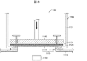
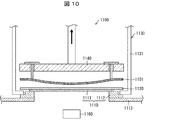
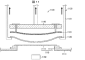
- FIG. 5 is a flow chart schematically showing a vapor deposition process in the vapor deposition apparatus 1100 of the comparative example shown in FIG. 6 to 11 are cross-sectional views taken along the longitudinal direction of the substrate, schematically showing each part of the vapor deposition process shown in FIG.
- step S31 when the substrate 1120 is carried into the vapor deposition apparatus 1100 (step S31), it is sandwiched between the hook 1131 of the elevating apparatus 1130 and the touch plate 1101. Then, in the sandwiched state, the substrate 1120 is carried directly above the vapor deposition mask 1110 so as to be separated from the vapor deposition mask 1110.
- the substrate 1120 is brought close to the vapor deposition mask 1110, and the substrate 1120 is aligned with the vapor deposition mask 1110 (step S32).
- the alignment device that performs alignment first images the alignment marks of the vapor deposition mask 1110 and the substrate 1120 with a camera, and the amount of deviation of the alignment marks of the substrate 1120 with respect to the alignment marks of the vapor deposition mask 1110 from the imaging data. Is measured (step S33). Then, the discrimination unit determines whether the deviation amount is within the threshold range (first allowable range) (step S34).
- step S35 the control unit of the alignment device controls the deviation amount to be 0 and horizontally moves the substrate 1120 to the alignment drive mechanism (step S35). Subsequently, the alignment device repeats steps S33 and S34. If the deviation amount is within the threshold range (Yes) in step S34, the alignment device ends the alignment (step S32).
- the touch plate 1101 presses the substrate 1120 toward the mask sheet 1111 by its own weight. Therefore, the touch plate 1101 and the substrate 1120 are bent downwardly in the direction of gravity together due to their own weight.
- the amount of deviation of the alignment mark of the substrate 1120 with respect to the alignment mark of the vapor deposition mask 1110 is measured in a state where the substrate 1120 is separated from the mask sheet 1111 of the vapor deposition mask 1110. ii) It means that it is determined whether the deviation amount is within the threshold range, and (iii) the deviation amount 0 is controlled as a target to move the substrate 1120 in the horizontal direction. Further, since the substrate 1120 is lowered onto the vapor deposition mask 1110 in a state where the substrate 1120 is in contact with the touch plate 1101 (step S36), the alignment (step S32) is also in a state where the substrate 1120 is in contact with the touch plate 1101. It is done in.
- the substrate 1120 is lowered onto the vapor deposition mask 1110 in a bent state together with the touch plate 1101 (step S36). During this time, the touch plate 1101 continues to press the substrate 1120 toward the vapor deposition mask 1110 by its own weight.
- the magnet 1140 is brought closer to the touch plate 1101 (step S37).
- the magnetic force of the magnet 1140 acting on the mask sheet 1111 increases, so that the mask sheet 1111 is pulled up.
- the touch plate 1101 continues to press the substrate 1120 toward the vapor deposition mask 1110 by its own weight.
- the mask sheet 1111 comes into close contact with the substrate 1120.
- the alignment position confirmation for confirming the position of the alignment mark is performed (step S38).
- the alignment device for confirming the alignment position captures an alignment mark with a camera, measures the amount of deviation (step S39), and determines whether the amount of deviation is within the threshold range (second allowable range) (step S40).
- the substrate 1120, the touch plate 1101 and the magnet 1140 are pulled up to separate the substrate 1120 from the vapor deposition mask 1110 (step S41), return to the alignment (step S32), and step. S35, S33, and S34 are performed again.
- alignment position confirmation means (i) alignment of the substrate 1120 with respect to the alignment mark of the vapor deposition mask 1110 in a state where the hook 1131 of the elevating device 1130 is lowered and the substrate 1120 is in contact with the vapor deposition mask 1110. It means that the amount of deviation of the mark is measured, and (ii) it is determined whether the amount of deviation is within the threshold range.
- the threshold range for alignment position confirmation is wider than the threshold range for alignment.
- step S40 the mask sheet 1111 of the vapor deposition mask 1110 is pulled up by the magnetic force of the magnet 1140, and the substrate 1120 is pressed by the weight of the touch plate 1101. Therefore, the mask sheet 1111 is in close contact with the substrate 1120. Then, when it is within the threshold range (Yes) in step S40, the film is formed by depositing the vapor deposition material on the substrate 1120 in such a close contact state (step S42).
- the magnet 1140 is lifted to separate the magnet 1140 from the touch plate 1101 (step S43). As a result, the magnetic force from the magnet 1140 acting on the vapor deposition mask 1110 is weakened, so that the mask sheet 1111 does not adhere to the substrate 1120.
- step S44 the touch plate 1101 is lifted and the touch plate 1101 is separated from the substrate 1120.
- the touch plate 1101 does not press the substrate 1120.
- step S45 the substrate 1120 is lifted (step S45), and the substrate 1120 is carried out (step S46).
- step S36 when the substrate 1120 is brought into contact with the vapor deposition mask 1110 in step S36, first, the central portion of the substrate 1120 is placed on the vapor deposition mask 1110 in a state of being bent by the weight of the substrate 1120. It had been. Then, the substrate 1120 is gradually placed on the vapor deposition mask 1110 in the direction from the central portion to both ends of the substrate 1120, the entire surface of the substrate 1120 is in contact with the vapor deposition mask 1110, and then the alignment position in step S38. Confirmation was being made.
- the substrate alignment marks provided at both ends may be significantly deviated from the mask alignment marks due to the bending of the central portion.
- these substrate alignment marks and mask alignment marks deviated from the permissible range There were cases where these substrate alignment marks and mask alignment marks deviated from the permissible range.
- FIG. 12 is a cross-sectional view of the substrate 120 along the longitudinal direction showing an example of a schematic configuration of the vapor deposition apparatus 100 according to the first embodiment of the present invention.
- the vapor deposition apparatus 100 includes a transport mechanism, a vacuum chamber, a control mechanism, and the like for transporting the substrate 120.
- FIG. 13 is a perspective view showing a schematic configuration of the vapor deposition apparatus 100 shown in FIG.
- the magnet 140, the touch plate 101, the substrate 120, the vapor deposition mask 110, and the hook 131 are shown, and the other configurations are not shown.
- the thin-film deposition apparatus 100 uses a thin-film deposition source 160 for vaporizing or sublimating a vapor-deposited material, a thin-film deposition mask 110 including a mask sheet 111 and a mask frame 112, and a mask sheet 111 on a substrate 120.
- the elevating device 130 includes a plurality of hooks 131 (support members) provided around the substrate 120, and a plurality of hook drive mechanisms 132 (drive mechanisms) corresponding to each hook 131.
- Each hook 131 is provided around the substrate 120 and abuts on the non-deposited region other than the vapor-deposited surface of the substrate 120 at the tip portion 131a to support the substrate 120.
- Each hook drive mechanism 132 is connected to the corresponding hook 131 and can drive the corresponding hook 131 in the ascending / descending direction independently of the other hooks 131.
- the hook drive 132 includes a drive member such as a motor.
- the mask frame 112 is provided with a plurality of recesses 115 capable of accommodating the tip portion 131a of the hook 131.
- the tip portion 131a is housed in the recess 115, so that the substrate 120 does not prevent the substrate 120 from coming into contact with the mask sheet 111.
- the magnet 140 includes a permanent magnet and / or an electric magnet.
- the size of the magnet is preferably equal to or larger than that of the substrate 120.
- the magnet 140 can be moved up and down by the magnet drive mechanism 142 via the arm 141.
- the touch plate 101 is a single sheet member that can be elastically deformed.
- the touch plate 101 is made of, for example, titanium alloy or stainless steel, and the thickness of the touch plate 101 is, for example, 5 mm to 15 mm.
- the touch plate 101 is connected to the magnet 140 so that the touch plate 101 can move in the elevating direction with respect to the magnet 140. More specifically, as illustrated in FIGS. 18 to 20, the touch plate 101 is suspended from the magnet 140 so that the touch plate 101 can press the substrate 120 toward the mask sheet 111 by its own weight.
- a T-shaped connecting tool 161 for side view is engaged with the upper surface of the touch plate 101 at the lower end of a T-shaped vertical bar, and the magnet 140 is provided with a through hole 144 for connecting to connect.
- the touch plate 101 is suspended from the magnet 140 so that the T-shaped vertical bar of the tool 161 passes through the connecting through hole 144.
- the vapor deposition apparatus 100 may further include a drive mechanism for raising and lowering the touch plate 101 independently of the magnet 140.
- the substrate-side surface of the touch plate 101 which is the substrate-side surface, may be a smooth surface or an embossed surface.
- the substrate 120 is a transparent substrate such as a glass substrate.
- the substrate 120 is a substrate to be vapor-deposited and is a target of the vapor deposition process in the thin-film deposition apparatus 100.
- the central portion of the vapor deposition surface on the vapor deposition mask 110 side is the vapor deposition region, and the peripheral portion of the vapor deposition surface is the non-deposited region.
- the thin-film deposition region is used as a region for the tip portion 131a of the hook 131 to come into contact with the hook 131 and a region for providing an alignment mark.
- FIG. 14 is a block diagram showing an example of a schematic configuration of an alignment device 170 included in the vapor deposition device 100 shown in FIG.
- the alignment device 170 includes a camera 171, an alignment drive mechanism 172, a storage device 173, and an alignment control mechanism 180.
- the camera 171 is provided above the magnet 140 so that the alignment marks provided at each corner of the vapor deposition mask 110 and the substrate 120 can be imaged.
- Two cameras 171 may be provided at each corner, one for imaging in alignment and the other for imaging in alignment position confirmation.
- the camera 171 is provided with one in each corner, with the depth of field adjusted so that the alignment mark can be imaged in both alignment and alignment position confirmation.
- the alignment drive mechanism 172 moves the substrate 120 supported by the plurality of hooks 131 in the longitudinal direction and the lateral direction of the substrate 120 in the alignment and the alignment position confirmation.
- a mechanism for moving a plurality of hooks 131 in the longitudinal direction and the lateral direction of the substrate 120 may be added to the elevating device 130.
- the storage device 173 stores the threshold range for alignment and alignment position confirmation.
- the storage device 173 may be provided outside the alignment device 170.
- each threshold range may be incorporated in the first discrimination unit 181 to the fourth discrimination unit 184.
- the alignment control mechanism 180 is realized by hardware such as a CPU (central processing unit) and an MPU (microprocessor unit).
- the alignment control mechanism 180 shown in FIG. 14 (a) has a first determination unit 181 that performs a determination (step S34) in the alignment (step S32) and a determination (step S38) in the alignment position confirmation (step S38) in the close contact state described later.
- the second determination unit 182 that performs step S40), the third determination unit 183 that performs the determination (step S54) in the alignment position confirmation (step S52) for the first end portion 126 described later, and the second end portion 127 described later.
- (Alignment mark and through hole for imaging) 15 is a cross-sectional view (a) and a plan view (b) schematically showing the superposition of the alignment marks 114 and 125 shown in FIG. 14, the through hole 106 for imaging, and the viewing hole 143.
- alignment marks 114 mask alignment marks
- alignment marks 125 board alignment marks
- the alignment mark 125 of the substrate 120 is provided at a position corresponding to the alignment mark 114 of the mask frame 112. Since the substrate 120 is transparent, the camera 171 can image the alignment mark 114 of the mask frame 112 through the substrate 120.
- a through hole 106 for imaging and a viewing hole 143 are provided at each corner of the touch plate 101 and the magnet 140.
- the image pickup through hole 106 and the visual recognition hole 143 are provided at positions overlapping the alignment mark 114 of the mask frame 112. Therefore, as shown in FIG. 15, the camera 171 can image the alignment marks 114 and 125 of the mask frame 112 and the substrate 120 through the through hole 106 for imaging and the viewing hole 143 through the touch plate 101 and the magnet 140. ..
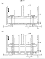
- FIG. 16 is a flow chart schematically showing an example of a thin-film deposition process for performing a thin-film deposition process in the thin-film deposition apparatus 100 shown in FIG. 12 including the alignment apparatus 170 shown in FIG. 17 to 20 are (a) cross-sectional views and (b) side views along the longitudinal direction of the substrate, schematically showing each part of the vapor deposition process in the vapor deposition apparatus shown in FIG.
- FIG. 17 (b), FIG. 18 (b), and FIG. 19 (b) these deflections are emphasized and illustrated so that the touch plate and the substrate are clearly bent. These are almost flat.
- the central portion of the substrate 120 is lowered and the substrate 120 is bent like a bowl. Further, as shown in FIG. 17B, the substrate 120 is supported from below by the tip portion 131a of the hook 131 at the peripheral portion. At this point, the substrate 120 is in a separated state in which the entire substrate 120 is separated from the mask sheet 111.
- the alignment device 170 performs alignment (step S32) after the substrate is carried in (step S31).
- the alignment device 170 that performs alignment first images the alignment marks 114 and 125 of the mask frame 112 and the substrate 120 with the camera 171 and determines the amount of deviation of the alignment mark 125 of the substrate 120 with respect to the alignment mark 114 of the vapor deposition mask 110 from the imaging data. Measure (step S33). Then, the first determination unit 181 determines whether the deviation amount is within the threshold range (first allowable range) (step S34).
- step S34 the alignment device 170 ends the alignment (step S32).
- step S32 the touch plate 101 presses the substrate 120 toward the mask sheet 111 by its own weight. Therefore, the touch plate 101 and the substrate 120 are bent downwardly in the direction of gravity together due to their own weight.
- “alignment” measures (i) the amount of deviation of the alignment mark 125 of the substrate 120 with respect to the alignment mark 114 of the vapor deposition mask 110 in a state where the substrate 120 is separated from the mask sheet 111 of the vapor deposition mask 110. , (Ii) It means that it is determined whether the deviation amount is within the threshold range, and (i) the deviation amount 0 is controlled as a target, and the substrate 120 is moved in the horizontal direction. Further, since the substrate 120 is lowered onto the vapor deposition mask 110 in a state where the substrate 120 is in contact with the touch plate 101 (steps S51, S56, S57), the substrate 120 also hits the touch plate 101 in the alignment (step S32). It is done in contact.
- the hook drive mechanism is such that the substrate 120 abuts on the mask sheet 111 only at the first end portion 126 in the longitudinal direction (first direction orthogonal to the elevating direction) of the substrate 120.
- the 132 drives the hook 131 that supports the substrate 120 (step S51, first driving step).
- step S51 first driving step.
- the second end portion 127 on the opposite side of the first end portion 126 and the intermediate portion 128 between the first end portion 126 and the second end portion 127 are separated from the mask sheet 111.
- the touch plate 101 presses the substrate 120, and at least the first end portion 101a of the touch plate 101 presses the first end portion 126 of the substrate 120 toward the mask sheet 111.
- the alignment device 170 confirms the alignment position of the first end portion 126 (step S52) in a state where only the first end portion 126 of the substrate 120 is in contact with the mask sheet 111. , 1st confirmation step) is executed.
- the alignment device 170 first captures the alignment marks 114 and 125 of the mask frame 112 and the substrate 120 on the first end 126 side with the camera 171, and from the imaging data, the alignment mark 114 of the substrate 120 with respect to the alignment mark 114 of the vapor deposition mask 1110.
- the amount of deviation of the alignment mark 125 is measured (step S53).
- the third determination unit 183 determines whether the deviation amount is within the threshold range (third allowable range) (step S54). If it is not within the threshold range (No), the substrate 120 and the touch plate 101 are pulled up to separate the substrate 120 from the vapor deposition mask 110 (step S55), and the process returns to alignment (step S32).
- the "alignment position confirmation for the first end portion 126" is performed on (i) the first end portion 126 of the substrate 120 in a state where only the first end portion 126 of the substrate 120 is in contact with the mask sheet 111. It means that the deviation amount of the provided alignment mark 125 with respect to the alignment mark 114 of the vapor deposition mask 110 is measured, and (ii) it is determined whether the deviation amount is within the threshold range.
- the threshold range for alignment position confirmation for the first end 126 is wider than the threshold range for alignment.
- step S54 when it was within the threshold range (Yes) in step S54, the intermediate portion 128 of the substrate 120 was gradually lowered from the first end portion 126 side to the second end portion 127 side.
- the hook drive mechanism 132 drives the hook 131 that supports the substrate 120 (step S56, the first half of the second drive step).
- step S56 the first half of the second drive step.
- the hook drive mechanism 132 (see FIG. 12) further drives the hook 131 supporting the substrate 120 so that the second end portion 127 of the substrate 120 comes into contact with the mask sheet 111 (step). S53, the latter half of the second drive step) is performed. As a result, the entire substrate 120 comes into contact with the mask sheet 111.
- the alignment device 170 confirms the alignment position of the second end portion 127 in a state where the entire substrate 120 is in contact with the mask sheet 111 (step S58, second confirmation step). ) Is executed.
- the alignment device 170 first captures the alignment marks 114 and 125 of the mask frame 112 and the substrate 120 on the second end 127 side with the camera 171, and from the imaging data, the alignment mark 114 of the substrate 120 with respect to the alignment mark 114 of the vapor deposition mask 110.
- the amount of deviation of the alignment mark 125 is measured (step S59).
- the fourth determination unit 184 determines whether the deviation amount is within the threshold range (fourth allowable range) (step S60). If it is not within the threshold range (No), the substrate 120 and the touch plate 101 are pulled up to separate the substrate 120 from the vapor deposition mask 110 (step S61), and the process returns to alignment (step S32).
- "confirmation of the alignment position for the second end 127" is performed in the state where both the first end 126 and the second end 127 of the substrate 120 are in contact with the mask sheet 111, and (i) the substrate 120. It means that the amount of deviation of the alignment mark 125 provided at the second end portion 127 of the vapor deposition mask 110 with respect to the alignment mark 114 is measured, and (ii) it is determined whether the deviation amount is within the threshold range.
- the threshold range in the alignment position confirmation for the second end 127 is wider than the threshold range in the alignment position confirmation for the first end 126 side.
- step S40 determines whether the substrate 120 is separated from the vapor deposition mask 110 by pulling up the substrate 120, the touch plate 101, and the magnet 140 (step S41), and the alignment (step S32) is returned.
- "confirmation of alignment position in close contact” means that (i) the amount of deviation of the alignment mark 125 of the substrate 120 with respect to the alignment mark 114 of the vapor deposition mask 110 while the substrate 120 is in close contact with the vapor deposition mask 110. It means measuring and (ii) determining whether the deviation amount is within the threshold range.
- the threshold range for the alignment position confirmation in the close contact state is wider than the threshold range for the alignment position confirmation for the second end portion 127.
- step S40 If it is within the threshold range in step S40 (Yes), the film is formed by depositing a vapor deposition material on the substrate 120 with the mask sheet 111 in close contact with the substrate 120 (step S42). After the vapor deposition is completed, magnet separation (step S43) and touch plate separation (step S44) are performed in this order, and the substrate 120 is lifted (step S45) to carry out the substrate 1120 (step S46).
- FIG. 21 is a block diagram showing another example of the schematic configuration of the alignment device 170 included in the vapor deposition device 100 shown in FIG.
- the alignment control mechanism 180 of the alignment device 170 shown in FIG. 21 confirms the alignment position of both the first determination unit 181 and the second determination unit 182, and the first end portion 126 and the second end portion 127 described later (step).
- a fifth determination unit 185 that performs the determination (step S64) in S62) and a control unit 186 are provided.
- FIG. 22 is a flow chart schematically showing another example of the vapor deposition process in the vapor deposition apparatus 100 shown in FIG. 12 including the alignment apparatus 170 shown in FIG. 21.
- the first end 126 and the second end Alignment position confirmation (S62) is performed for both parts 127.
- the alignment device 170 (see FIG. 21) is subjected to the substrate Alignment position confirmation (step S62, confirmation step) for both the first end portion 126 and the second end portion 127 is executed in a state where the entire 120 is in contact with the mask sheet 111.
- the alignment device 170 first captures the alignment marks 114 and 125 of the mask frames 112 and the substrate 120 on both ends 126 and 127 sides with the camera 171 and uses the imaging data to capture the alignment marks 114 of the substrate 120 with respect to the alignment marks 114 of the vapor deposition mask 110.
- the amount of deviation of the alignment mark 125 is measured (step S63). Then, the fifth determination unit 185 determines whether the deviation amount is within the threshold range (fifth allowable range) (step S64). If it is not within the threshold range (No), the substrate 120 and the touch plate 101 are pulled up to separate the substrate 120 from the vapor deposition mask 110 (step S65), return to the alignment (step S32), and step S35 to step. S37 is performed again.
- both the first end portion 126 and the second end portion 127 of the substrate 120 are in contact with the mask sheet 111.
- the threshold range in the alignment position confirmation for both the first end portion 126 and the second end portion 127 is wider than the threshold range in the alignment and narrower than the threshold range in the threshold range in the alignment position confirmation in the close contact state.
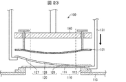
- FIG. 23 is a cross-sectional view taken along the longitudinal direction of the substrate 120, showing a case where the touch plate 101 does not press the substrate 120 in the substrate lowering step. As shown in FIG. 22, the substrate 120 may be gradually lowered along the longitudinal direction without being pressed by the touch plate 101.
- the example according to the first embodiment is not limited to this.
- the substrate 120 may be gradually lowered, for example, along the lateral direction.
- FIG. 24 is a cross-sectional view of the substrate 120 along the longitudinal direction showing an example of the schematic configuration of the vapor deposition apparatus 200 according to the second embodiment of the present invention.
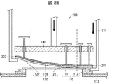
- FIG. 25 is a cross-sectional view taken along the longitudinal direction of the substrate 120, schematically showing a part of the substrate descent in the vapor deposition process in the vapor deposition apparatus 200 shown in FIG. 24.
- the vapor deposition apparatus 200 according to the second embodiment is different from the vapor deposition apparatus 100 according to the first embodiment, and has a touch plate 201 (first sheet member) and a touch plate 202 (second sheet member). It is equipped with two touch plates.
- the other configuration is that the thin-film deposition apparatus 200 according to the second embodiment is the same as the vapor deposition apparatus 100 according to the first embodiment.
- the two touch plates 201 and 202 are arranged along the longitudinal direction of the substrate 120.
- One touch plate 201 is one first sheet member arranged corresponding to the first end portion 126 of the substrate 120
- the other touch plate 202 is the second end portion 127 and the intermediate portion of the substrate 120. It is one second sheet member arranged corresponding to 128.
- One touch plate 201 may be elastically deformable without being substantially elastically deformed.
- the other touch plate 202 has a longer dimension than the one touch plate 201 in the longitudinal direction of the substrate 120 and is elastically deformable.
- the substrate 120 is first lowered so as to come into contact with the mask sheet 111 only at the first end portion 126. At this time, it is preferable that the touch plate 201 presses the first end portion 126 of the substrate 120 toward the mask sheet 111. Similar to the first embodiment, the substrate 120 is subsequently gradually lowered from the first end 126 side to the second end 127 side of the intermediate portion 128, and finally the second end portion 127. To.
- the example according to the second embodiment is not limited to this, and two touch plates 201 and 202 may be arranged along the lateral direction, for example, and gradually lowered along the arrangement direction.
- FIG. 26 is a cross-sectional view of the substrate 120 along the longitudinal direction showing an example of a schematic configuration of the vapor deposition apparatus 300 according to the third embodiment of the present invention.
- FIG. 25 is a cross-sectional view taken along the longitudinal direction of the substrate 120 which schematically shows an example of the vapor deposition process in the vapor deposition apparatus 300 shown in FIG.
- the vapor deposition apparatus 300 according to the third embodiment includes four touch plates 301, 302, 303, 303, unlike the vapor deposition apparatus 100, 200 according to the first and second embodiments described above.
- the other configurations of the vapor deposition apparatus 300 according to the third embodiment are the same as those of the vapor deposition apparatus 100 and 200 according to the first and second embodiments.
- the four touch plates 301, 302, 303, 303 are arranged along the longitudinal direction of the substrate 120.
- One touch plate 301 is one first sheet member arranged corresponding to the first end 126 of the substrate 120, and another touch plate 302 is attached to the second end 127 of the substrate 120. It is one second sheet member arranged correspondingly, and the remaining touch plates 303 and 303 (third sheet member) are two third sheets arranged corresponding to the intermediate portion 128 of the substrate 120. It is a member.
- the number of third sheet members arranged corresponding to the intermediate portion 128 is not limited to two, and may be one or three or more. Further, the third sheet members arranged corresponding to the intermediate portion 128 may have different widths in the longitudinal direction from each other.
- Each of the touch plates 301, 302, and 303 may be elastically deformable without being substantially elastically deformed.
- the dimensions of the touch plates 301, 302, 303 that is, the dimensions of the first sheet member, the second sheet member, and the third sheet member are the same as each other.
- the seat members having the same configuration can be used for any of the first seat member, the second seat member, and the third seat member.
- the substrate 120 is first lowered so as to come into contact with the mask sheet 111 only at the first end portion 126. At this time, it is preferable that the touch plate 301 presses the first end portion 126 of the substrate 120 toward the mask sheet 111. Similar to the first embodiment, the substrate 120 is subsequently gradually lowered from the first end 126 side to the second end 127 side of the intermediate portion 128, and finally the second end portion 127. To.
- the example according to the third embodiment is not limited to this, and the touch plates 301, 302, and 303 may be arranged along the lateral direction, for example, and gradually lowered along the arrangement direction.
- FIG. 28 is a cross-sectional view of the substrate 120 along the longitudinal direction showing an example of a schematic configuration of the vapor deposition apparatus 400 according to the fourth embodiment of the present invention.
- FIG. 29 is a cross-sectional view taken along the longitudinal direction of the substrate 120, schematically showing an example of substrate descent in the vapor deposition step in the vapor deposition apparatus 400 shown in FIG. 28.
- the vapor deposition apparatus 400 according to the fourth embodiment includes three touch plates 401, 402, 403, unlike the vapor deposition apparatus 100, 200, 300 according to the above-described first to third embodiments.
- Other configurations are the same as the vapor deposition apparatus 400 according to the fourth embodiment as the vapor deposition apparatus 100, 200, 300 according to the first to third embodiments.
- the three touch plates 401, 402, and 403 are arranged along the longitudinal direction of the substrate 120.
- One touch plate 401 is one first sheet member arranged corresponding to the first end 126 of the substrate 120, and another touch plate 402 is on the second end 127 of the substrate 120. It is one second sheet member arranged correspondingly, and the remaining touch plate 403 is one third sheet member arranged corresponding to the entire intermediate portion 128 of the substrate 120.
- the touch plate 401 arranged corresponding to the first end portion 126 may be elastically deformable without being substantially elastically deformed.
- the touch plate 402 arranged corresponding to the second end portion 127 may be elastically deformable without being substantially elastically deformed.
- the touch plate 403 arranged corresponding to the intermediate portion 128 has a longer dimension than the touch plates 401 and 402 in the longitudinal direction of the substrate 120 and is elastically deformable.
- the substrate 120 is first lowered so as to come into contact with the mask sheet 111 only at the first end portion 126. At this time, it is preferable that the touch plate 401 presses the first end portion 126 of the substrate 120 toward the mask sheet 111. Similar to the first embodiment, the substrate 120 is subsequently gradually lowered from the first end 126 side to the second end 127 side of the intermediate portion 128, and finally the second end portion 127. To.
- the example according to the fourth embodiment is not limited to this, and the touch plates 401, 402, 403 may be arranged along the lateral direction, for example, and may be gradually lowered along the arrangement direction.
- the thin-film deposition apparatus is arranged between a thin-film deposition source, a thin-film deposition mask having a mask sheet and a mask frame, a magnet for bringing the mask sheet into close contact with the substrate, and the substrate and the magnet.
- a vapor deposition apparatus including a touch plate, an elevating device for raising and lowering the substrate with respect to the vapor deposition mask, and an alignment device for aligning the vapor deposition mask with the substrate.
- a plurality of support members provided around the substrate and in contact with a non-deposited region other than the surface to be vapor-deposited of the substrate to support the substrate, and the plurality of support members connected to the plurality of support members.
- a drive mechanism for driving the members independently of each other in the elevating direction of the substrate is provided, and the drive mechanism is such that the substrate is pressed by the touch plate and only one end of the substrate is vapor-deposited. While driving the support member so as to abut the mask and pressing the substrate with the touch plate, the other end gradually hits the vapor deposition mask toward the other end of the substrate. The support member is driven so as to be in contact with the support member.
- the touch plate may be configured to be one sheet member that can be elastically deformed.
- the vapor deposition apparatus may have a configuration in which the touch plate is a plurality of sheet members arranged along the longitudinal direction thereof in the above aspect 1.
- the vapor deposition apparatus may have a configuration in which the dimensions of each of the plurality of sheet members in the longitudinal direction are the same as each other in the above aspect 3.
- the plurality of sheet members are the first sheet member and the first sheet member arranged on the one end portion and the other end portion side of the substrate, respectively.
- the configuration may include two seat members.
- the dimension of the second sheet member in the longitudinal direction may be longer than the dimension of the first sheet member in the longitudinal direction. Good.
- the second sheet member may be a single sheet member that can be elastically deformed.
- the plurality of sheet members are the first sheet member and the first sheet member arranged on the one end portion and the other end portion side of the substrate, respectively.
- the configuration may further include a two-seat member and a third seat member arranged between the first seat member and the second seat member.
- the dimensions of the third sheet member in the longitudinal direction are the dimensions of the first sheet member and the second sheet member in the longitudinal direction. It may be a longer configuration than that.
- the three sheet members may be configured to be one elastically deformable sheet member.
- the alignment device in any one of the above aspects 1 to 10, includes an imaging unit provided above the magnet in the elevating direction, and the substrate is , The one end and the other end are provided with a substrate alignment mark, the vapor deposition mask is provided with a mask alignment mark corresponding to the substrate alignment mark, and the touch plate is provided with the imaging unit.
- the substrate alignment mark and the mask alignment mark may be configured to have an imaging through hole for imaging.
- the thin-film deposition apparatus may have a structure in which the magnet is formed with a visible hole superimposing on the image pickup through hole of the touch plate.
- the vapor deposition apparatus further includes a magnet driving mechanism for driving the magnet in the elevating direction with respect to the substrate in any one of the above aspects 1 to 12, and the touch plate is the touch plate. It may be configured to be connected to the magnet so as to be movable in the elevating direction with respect to the magnet.
- the thin-film deposition apparatus hangs the touch plate movably from the magnet so that the touch plate can press the substrate toward the mask sheet by its own weight. It may be a lowered configuration.
- the mask frame is provided with a plurality of recesses capable of accommodating the tip portions of the plurality of support members. It may be configured.
- the method for manufacturing a display device is a method for manufacturing a display device having a substrate, which comprises a vapor deposition step of performing a vapor deposition process on the substrate by using a vapor deposition mask.
- the first driving step of driving the support member supporting the substrate so that only one end of the substrate abuts on the vapor deposition mask while the substrate is pressed by the touch plate, and the touch plate A second driving step of driving the support member so that the other end of the substrate gradually abuts on the vapor deposition mask while pressing the substrate is included.
- one end of the substrate abuts on the thin-film deposition mask between the first driving step and the second driving step.
- the first confirmation step of confirming the alignment position between the substrate alignment mark provided at one end and the mask alignment mark provided on the vapor deposition mask is executed, and after the second drive step, Second, the alignment position between the substrate alignment mark provided on the other end and the mask alignment mark provided on the vapor deposition mask is confirmed in a state where the other end of the substrate is in contact with the vapor deposition mask. It may be a method of executing the confirmation process.
- one end and the other end of the substrate are in contact with the vapor deposition mask after the second driving step.
- Display device 100, 200, 300, 400 Thin film deposition equipment 101 Touch plate 106 Through hole for imaging 110 Vapor deposition mask 111 Mask sheet 112 Mask frame 114 Alignment mark (mask alignment mark) 115 Recess 120 Substrate 125 Alignment mark (Board alignment mark) 126 1st end 127 2nd end 128 Intermediate 130 Lifting device 131 Hook (support member) 131a Tip 132 Hook drive mechanism (drive mechanism) 140 Magnet 142 Magnet drive mechanism 143 Visual recognition hole 171 Camera (imaging unit) 160 Thin-film deposition sources 201, 301, 401 Touch plate (first sheet member) 202, 302, 402 Touch plate (second sheet member) 303, 403 Touch plate (third sheet member)
Landscapes
- Chemical & Material Sciences (AREA)
- Chemical Kinetics & Catalysis (AREA)
- Engineering & Computer Science (AREA)
- Materials Engineering (AREA)
- Mechanical Engineering (AREA)
- Metallurgy (AREA)
- Organic Chemistry (AREA)
- Electroluminescent Light Sources (AREA)
Abstract
蒸着装置(100)では、基板(120)は、第1端部(126)のみでマスクシート(111)に当接し、第1端部(126)から第2端部(127)に向って徐々に基板(120)の全体でマスクシート(111)に当接するように、下降される。第1端部(126)のみがマスクシート(111)に当接しているとき、タッチプレート(101)の少なくとも一部(101a)は、マスクシート(111)に向って基板(120)を押圧する。
Description
本発明は、蒸着装置、および表示装置の製造方法に関する。
特許文献1,2には、蒸着マスクとマグネットとの間に基板が配置され、マグネットの磁力によって、蒸着マスクが基板に密着する蒸着装置が開示されている。
ところで、上記のような従来の蒸着装置では、蒸着処理を高精度に行うために、蒸着処理対象物である、基板の両端部に設けられた基板アライメントマークと、蒸着マスクに設けられたマスクアライメントマークとが予め定められた許容範囲に存在するか否かを確認するアライメント位置確認を、蒸着処理を実行する前に行うことが知られている。
ところが、上記のような従来の蒸着装置では、上記アライメント位置確認を効率よく行うことができずに、その蒸着処理、ひいては表示装置の製造時間を短縮することができないという問題を生じることがあった。
具体的にいえば、従来の蒸着装置では、蒸着マスクに基板を当接させる場合に、まず、基板の中央部が当該基板の自重によって撓んだ状態で蒸着マスク上に載置されていた。その後、従来の蒸着装置では、基板の中央部から両端部に向かう方向で、当該基板が徐々に蒸着マスク上に載置されて、基板の全面が蒸着マスクに当接した後、アライメント位置確認が行われていた。このため、従来の蒸着装置では、アライメント位置確認を行う場合に、中央部の撓みに起因して、両端部に設けられた基板アライメントマークがマスクアライメントマークに対して大きくズレを生じることがあり、これらの基板アライメントマークとマスクアライメントマークとが許容範囲から逸脱することがあった。この結果、蒸着マスクから基板を再度離間させて、上記許容範囲となるまでアライメント位置確認を繰り返し行う必要が発生して、蒸着処理、及び表示装置の製造時間を短縮することができないという問題を生じることがあった。
本発明は、上記の問題点に鑑みてなされたものであり、その目的は、表示装置の製造時間を短縮することができる蒸着装置および表示装置の製造方法を実現することにある。
本発明の一実施形態に係る蒸着装置は、蒸着源と、マスクシート及びマスクフレームを有する蒸着マスクと、前記マスクシートを基板に密接させるためのマグネットと、前記基板と前記マグネットとの間に配置されるタッチプレートと、前記蒸着マスクに対して、前記基板を昇降する昇降装置と、前記蒸着マスクと前記基板とのアライメントを行うアライメント装置と、を備えた蒸着装置であって、前記昇降装置は、前記基板の周囲に設けられるとともに、前記基板の被蒸着面以外の非蒸着領域に当接して、当該基板を支持する複数の支持部材と、前記複数の支持部材に連結されて、前記複数の支持部材を、互いに独立して前記基板の昇降方向に駆動する駆動機構と、を備え、前記駆動機構は、前記タッチプレートで前記基板を押圧した状態で、前記基板の一方の端部のみが前記蒸着マスクに当接するように前記支持部材を駆動し、かつ、前記タッチプレートで前記基板を押圧した状態で、前記基板の他方の端部に徐々に向かって当該他方の端部が前記蒸着マスクに当接するように前記支持部材を駆動する、構成である。
本発明の一実施形態に係る表示装置の製造方法は、基板を有する表示装置の製造方法であって、蒸着マスクを用いて、前記基板に蒸着処理を行う蒸着工程を備え、前記蒸着工程には、タッチプレートで前記基板を押圧した状態で、前記基板の一方の端部のみが前記蒸着マスクに当接するように、当該基板を支持する支持部材を駆動する第1駆動工程と、前記タッチプレートで前記基板を押圧した状態で、前記基板の他方の端部に徐々に向かって当該他方の端部が前記蒸着マスクに当接するように、前記支持部材を駆動する第2駆動工程と、が含まれる、方法である。
本発明の幾つかの態様によれば、表示装置の製造時間を短縮することができる蒸着装置および表示装置の製造方法を実現することができる。
(表示デバイスの製造方法及び構成)
以下においては、「同層」とは同一のプロセス(成膜工程)にて形成されていることを意味し、「下層」とは、比較対象の層よりも先のプロセスで形成されていることを意味し、「上層」とは比較対象の層よりも後のプロセスで形成されていることを意味する。
以下においては、「同層」とは同一のプロセス(成膜工程)にて形成されていることを意味し、「下層」とは、比較対象の層よりも先のプロセスで形成されていることを意味し、「上層」とは比較対象の層よりも後のプロセスで形成されていることを意味する。
図1は表示デバイスの製造方法の一例を示すフローチャートである。図2は、表示デバイス2の表示領域の構成を示す断面図である。
フレキシブルな表示デバイスを製造する場合、図1および図2に示すように、まず、透光性の支持基板(例えば、マザーガラス)上に樹脂層12を形成する(ステップS1)。次いで、バリア層3を形成する(ステップS2)。次いで、TFT層4を形成する(ステップS3)。次いで、トップエミッション型の発光素子層5を形成する(ステップS4)。次いで、封止層6を形成する(ステップS5)。次いで、封止層6上に上面フィルムを貼り付ける(ステップS6)。
次いで、レーザ光の照射等によって支持基板を樹脂層12から剥離する(ステップS7)。次いで、樹脂層12の下面に下面フィルム10を貼り付ける(ステップS8)。次いで、下面フィルム10、樹脂層12、バリア層3、TFT層4、発光素子層5、封止層6を含む積層体を分断し、複数の個片を得る(ステップS9)。次いで、得られた個片に機能フィルム39を貼り付ける(ステップS10)。次いで、複数のサブ画素が形成された表示領域よりも外側(非表示領域、額縁領域)の一部(端子部)に電子回路基板(例えば、ICチップおよびFPC)をマウントする(ステップS11)。なお、ステップS1~S11は、表示デバイス製造装置(ステップS1~S5の各工程を行う成膜装置を含む)が行う。
樹脂層12の材料としては、例えばポリイミド等が挙げられる。樹脂層12の部分を、二層の樹脂膜(例えば、ポリイミド膜)およびこれらに挟まれた無機絶縁膜で置き換えることもできる。
バリア層3は、水、酸素等の異物がTFT層4および発光素子層5に侵入することを防ぐ層であり、例えば、CVD法により形成される、酸化シリコン膜、窒化シリコン膜、あるいは酸窒化シリコン膜、またはこれらの積層膜で構成することができる。
TFT層4は、半導体膜15と、半導体膜15よりも上層の無機絶縁膜16(ゲート絶縁膜)と、無機絶縁膜16よりも上層の、ゲート電極GEおよびゲート配線GHと、ゲート電極GEおよびゲート配線GHよりも上層の無機絶縁膜18と、無機絶縁膜18よりも上層の容量電極CEと、容量電極CEよりも上層の無機絶縁膜20と、無機絶縁膜20よりも上層のソース配線SHと、ソース配線SHよりも上層の平坦化膜21(層間絶縁膜)とを含む。
半導体膜15は、例えば低温ポリシリコン(LTPS)あるいは酸化物半導体(例えばIn-Ga-Zn-O系の半導体)で構成され、半導体膜15およびゲート電極GEを含むようにトランジスタ(TFT)が構成される。図2では、トランジスタがトップゲート構造で示されているが、ボトムゲート構造でもよい。
ゲート電極GE、ゲート配線GH、容量電極CE、およびソース配線SHは、例えば、アルミニウム、タングステン、モリブデン、タンタル、クロム、チタン、および銅の少なくとも1つを含む金属の単層膜あるいは積層膜によって構成される。図2のTFT層4には、一層の半導体層および三層のメタル層が含まれる。
無機絶縁膜16・18・20は、例えば、CVD法によって形成された、酸化シリコン(SiOx)膜あるいは窒化シリコン(SiNx)膜またはこれらの積層膜によって構成することができる。平坦化膜21は、例えば、ポリイミド、アクリル等の塗布可能な有機材料によって構成することができる。
発光素子層5は、平坦化膜21よりも上層のアノード22(陽極)と、アノード22のエッジを覆う絶縁性のエッジカバー23と、エッジカバー23よりも上層のEL(エレクトロルミネッセンス)する活性層24と、活性層24よりも上層のカソード25(陰極)とを含む。エッジカバー23は、例えば、ポリイミド、アクリル等の有機材料を塗布した後にフォトリソグラフィよってパターニングすることで形成される。
サブ画素ごとに、島状のアノード22、活性層24、およびカソード25を含み、QLEDである発光素子ES(電界発光素子)が発光素子層5に形成され、発光素子ESを制御するサブ画素回路がTFT層4に形成される。
活性層24は、例えば、下層側から順に、正孔注入層、正孔輸送層、発光層、電子輸送層、電子注入層を積層することで構成される。発光層は、蒸着法あるいはインクジェット法によって、エッジカバー23の開口(サブ画素ごと)に、島状に形成される。他の層は、島状あるいはベタ状(共通層)に形成する。また、正孔注入層、正孔輸送層、電子輸送層、電子注入層のうち1以上の層を形成しない構成も可能である。
QLEDの発光層は、例えば、量子ドットを分散させた溶媒をインクジェット塗布することで、島状の発光層(1つのサブ画素に対応)を形成することができる。
アノード22は、例えばITO(Indium Tin Oxide)とAg(銀)あるいはAgを含む合金との積層によって構成されたり、AgまたはAlを含む材料から構成されたりして、光反射性を有する反射電極である。カソード(陰極)25は、Ag、Au、Pt、Ni、Irの薄膜、MgAg合金の薄膜、ITO、IZO(Indium zinc Oxide)等の透光性の導電材で構成された透明電極である。表示デバイスがトップエミッション型でなく、ボトムエミッション型の場合、下面フィルム10および樹脂層12が透光性であり、アノード22が透明電極であり、カソード25が反射電極である。
発光素子ESでは、アノード22およびカソード25間の駆動電流によって正孔と電子が発光層内で再結合し、これによって生じたエキシトンが、量子ドットの伝導帯準位(conduction band)から価電子帯準位(valence band)に遷移する過程で光(蛍光)が放出される。
封止層6は透光性であり、カソード25を覆う無機封止膜26と、無機封止膜26よりも上層の有機バッファ膜27と、有機バッファ膜27よりも上層の無機封止膜28とを含む。発光素子層5を覆う封止層6は、水、酸素等の異物の発光素子層5への浸透を防いでいる。
無機封止膜26および無機封止膜28はそれぞれ無機絶縁膜であり、例えば、CVD法により形成される、酸化シリコン膜、窒化シリコン膜、あるいは酸窒化シリコン膜、またはこれらの積層膜で構成することができる。有機バッファ膜27は、平坦化効果のある透光性有機膜であり、アクリル等の塗布可能な有機材料によって構成することができる。有機バッファ膜27は例えばインクジェット塗布によって形成することができるが、液滴を止めるためのバンクを非表示領域に設けてもよい。
下面フィルム10は、支持基板を剥離した後に樹脂層12の下面に貼り付けることで柔軟性に優れた表示デバイスを実現するための、例えばPETフィルムである。機能フィルム39は、例えば、光学補償機能、タッチセンサ機能、および保護機能の少なくとも1つを有する。
以上にフレキシブルな表示デバイスについて説明したが、非フレキシブルな表示デバイスを製造する場合は、一般的に樹脂層の形成、基材の付け替え等が不要であるため、例えば、ガラス基板上にステップS2~S5の積層工程を行い、その後ステップS9に移行する。また、非フレキシブルな表示デバイスを製造する場合は、封止層6を形成する代わりに或いは加えて、透光性の封止部材を、封止接着剤によって、窒素雰囲気下で接着してもよい。透光性の封止部材は、ガラスおよびブラスチックなどから形成可能であり、凹形状であることが好ましい。
本発明の一実施形態は、特に、上述した表示デバイス(表示装置)の製造方法のうち、ステップS4における蒸着処理に関する。また、本発明の一実施形態は、特に、蒸着処理に用いられる蒸着装置に関する。
(比較例)
図3は、比較例の蒸着装置1100の概略構成を示す、基板1120の長手方向に沿った断面図である。なお、簡便のために図示を省略するが、蒸着装置1100は、基板1120を搬送するための搬送機構、真空チャンバー、および制御機構などを備える。また、以後の図面においても同様に図示を省略する。
図3は、比較例の蒸着装置1100の概略構成を示す、基板1120の長手方向に沿った断面図である。なお、簡便のために図示を省略するが、蒸着装置1100は、基板1120を搬送するための搬送機構、真空チャンバー、および制御機構などを備える。また、以後の図面においても同様に図示を省略する。
図3に示すように、比較例の蒸着装置1100は、蒸着源1160と、蒸着マスク1110を保持するマスクホルダー1113と、基板1120を昇降可能に保持する昇降装置1130と、マグネット1140と、タッチプレート1101と、を備え、
前記蒸着マスク1110はマスクシート1111とマスクフレーム1112とを含む。
前記蒸着マスク1110はマスクシート1111とマスクフレーム1112とを含む。
図4は、図3に示した比較例の蒸着装置1100が備えるタッチプレート1101の基板側表面1104の概略形状を示す拡大側面図である。
図4に示すように、比較例のタッチプレート1101の基板側表面1104は、平坦面1150に陥凹も突起も設けられておらず、平滑な表面である。このため、タッチプレート1101は基板1120に、基板側表面1104全体で当接(面接触)できる。
タッチプレート1101は、例えば、チタン合金またはステンレス鋼から形成される。これに対して、基板1120は、例えば、ガラス基板である。このため、基板1120の可撓性は、タッチプレート1101の可撓性よりも、高い。
図5は、図3に示した比較例の蒸着装置1100における蒸着工程を概略的に示すフロー図である。図6~図11は、図5に示した蒸着工程の各部分を概略的に示す、基板の長手方向に沿った断面図である。
図5に示すように、基板1120は、蒸着装置1100内に搬入される(ステップS31)と、昇降装置1130のフック1131とタッチプレート1101との間に挟まれる。そして、挟まれた状態で、基板1120は、蒸着マスク1110の直上に、蒸着マスク1110から離間するように、運ばれる。
そして、図6に示すように、基板1120を蒸着マスク1110に近づけて、基板1120を蒸着マスク1110に対してアライメントするアライメントが行われる(ステップS32)。図5に示すように、アライメントを行うアライメント装置は、まず、カメラで蒸着マスク1110および基板1120のアライメントマークを撮像して、撮像データから蒸着マスク1110のアライメントマークに対する基板1120のアライメントマークのズレ量を測定する(ステップS33)。そして、判別部でズレ量が閾値範囲(第1許容範囲)内か判別する(ステップS34)。閾値範囲内で無かった(No)場合、アライメント装置の制御部は、ズレ量0を目標に制御して、アライメント駆動機構に基板1120を水平移動させる(ステップS35)。続いて、アライメント装置はステップS33,S34を繰り返す。ステップS34でズレ量が閾値範囲内であった(Yes)場合、アライメント装置はアライメント(ステップS32)を終了する。
アライメント(ステップS32)の間、タッチプレート1101は自重によって、基板1120をマスクシート1111側に押圧している。そのため、タッチプレート1101および基板1120は、自重によって一緒に、重力方向である下向きに凸に撓んでいる。
本比較例において「アライメント」は、基板1120が蒸着マスク1110のマスクシート1111から離間している状態で、(i)蒸着マスク1110のアライメントマークに対する基板1120のアライメントマークのズレ量を測定し、(ii)該ズレ量が閾値範囲内か判別し、(iii)ズレ量0を目標に制御して、基板1120を水平方向に移動することを意味する。また、基板1120がタッチプレート1101に当接している状態で基板1120を蒸着マスク1110の上に降ろす(ステップS36)ので、アライメント(ステップS32)も、基板1120がタッチプレート1101に当接している状態で行われる。
図7に示すように、アライメント終了後、基板1120は、タッチプレート1101と共に撓んだ状態で、蒸着マスク1110の上に降ろされる(ステップS36)。この間、タッチプレート1101は自重によって、基板1120を蒸着マスク1110側に押圧し続けている。
続いて、図8に示すように、マグネット1140をタッチプレート1101に近づける(ステップS37)。これによって、マスクシート1111に作用するマグネット1140の磁力が大きくなるので、マスクシート1111は引き上げられる。また、タッチプレート1101は自重によって、基板1120を蒸着マスク1110側に押圧し続けている。これらの結果、マスクシート1111は基板1120と密着する。そして、アライメントマークの位置を確認するアライメント位置確認が行われる(ステップS38)。アライメント位置確認を行うアライメント装置は、カメラでアライメントマークを撮像してズレ量を測定し(ステップS39)、判別部でズレ量が閾値範囲(第2許容範囲)内か判別する(ステップS40)。閾値範囲内で無かった(No)場合、基板1120とタッチプレート1101とマグネット1140とを引き上げることによって、蒸着マスク1110から基板1120を離間させて(ステップS41)、アライメント(ステップS32)に戻り、ステップS35・S33・S34が再度行われる。
本比較例において「アライメント位置確認」は、昇降装置1130のフック1131を下して、基板1120が蒸着マスク1110に当接している状態で、(i)蒸着マスク1110のアライメントマークに対する基板1120のアライメントマークのズレ量を測定し、(ii)ズレ量を閾値範囲内か判別することを意味する。アライメント位置確認における閾値範囲は、アライメントにおける閾値範囲よりも、広い。
図8に示した状態において、マグネット1140の磁力によって、蒸着マスク1110のマスクシート1111は引き上げられ、タッチプレート1101の自重によって、基板1120は押さえつけられる。このため、マスクシート1111が基板1120に密着している。そして、ステップS40で閾値範囲内であった(Yes)場合、このように密着した状態で、基板1120に蒸着材料を蒸着することによって成膜を行う(ステップS42)。
図9に示すように、蒸着完了後、マグネット1140を持ち上げて、タッチプレート1101からマグネット1140を分離するマグネット分離を行う(ステップS43)。これによって、蒸着マスク1110に作用するマグネット1140からの磁力が弱まるため、マスクシート1111が基板1120に密着しなくなる。
続いて、図10に示すように、マグネット1140をさらに持ち上げることによって、タッチプレート1101を持ち上げて、基板1120からタッチプレート1101を分離するタッチプレート分離を行う(ステップS44)。これによって、タッチプレート1101は、基板1120を押圧しなくなる。そして、図11に示すように、基板1120を持ち上げて(ステップS45)、基板1120を搬出する(ステップS46)。
このような蒸着装置1100では、ステップS36において蒸着マスク1110に基板1120を当接させる場合に、まず、基板1120の中央部が当該基板1120の自重によって撓んだ状態で蒸着マスク1110上に載置されていた。その後、基板1120の中央部から両端部に向かう方向で、当該基板1120が徐々に蒸着マスク1110上に載置されて、基板1120の全面が蒸着マスク1110に当接した後、ステップS38のアライメント位置確認が行われていた。このため、比較例の蒸着装置1100では、アライメント位置確認を行う場合に、中央部の撓みに起因して、両端部に設けられた基板アライメントマークがマスクアライメントマークに対して大きくズレを生じることがあり、これらの基板アライメントマークとマスクアライメントマークとが許容範囲から逸脱することがあった。この結果、蒸着マスクから基板を再度離間させて(ステップS41)、上記許容範囲となるまでアライメント位置確認(ステップS38)を繰り返し行う必要が発生して、蒸着処理、及び表示装置の製造時間を短縮することができないという問題を生じることがあった。
〔実施形態1〕
以下、本発明の一実施形態について、図面を参照しながら詳細に説明する。ただし、図面に示されている形状,寸法および相対配置などはあくまで例示に過ぎず、これらによってこの発明の範囲が限定解釈されるべきではない。
以下、本発明の一実施形態について、図面を参照しながら詳細に説明する。ただし、図面に示されている形状,寸法および相対配置などはあくまで例示に過ぎず、これらによってこの発明の範囲が限定解釈されるべきではない。
図12は、本発明の実施形態1に係る蒸着装置100の概略構成の一例を示す、基板120の長手方向に沿った断面図である。なお、簡便のために図示を省略するが、蒸着装置100は、基板120を搬送するための搬送機構、真空チャンバー、および制御機構などを備える。
図13は、図12に示した蒸着装置100の概略構成を示す斜視図である。なお、図示の簡便のために、マグネット140、タッチプレート101、基板120、蒸着マスク110、およびフック131のみを示し、その他の構成の図示を省略している。
図12および図13に示すように、蒸着装置100は、蒸着材料を気化または昇華するための蒸着源160と、マスクシート111とマスクフレーム112とを含む蒸着マスク110と、マスクシート111を基板120に密接させるためのマグネット140と、基板120とマグネット140との間に配置されるタッチプレート101と、蒸着マスク110に対して、基板120を昇降する昇降装置130と、カメラ171(撮像部)を用いて蒸着マスク110と基板120とのアライメントを行うアライメント装置(図14参照)と、を備えた蒸着装置である。
昇降装置130は、基板120の周囲に設けられた複数のフック131(支持部材)と、各フック131に対応する複数のフック駆動機構132(駆動機構)とを備える。各フック131は、基板120の周囲に設けられるとともに、先端部131aで基板120の被蒸着面以外の非蒸着領域に当接して、基板120を支持する。各フック駆動機構132は、対応するフック131に連結され、対応するフック131をその他のフック131から独立して、昇降方向に駆動できる。フック駆動機132は、例えば、モータなどの駆動部材を含む。
マスクフレーム112には、フック131の先端部131aを収容可能な複数の凹部115が設けられている。先端部131aは、凹部115に各々収容されることによって、基板120がマスクシート111に当接することを妨げない。
マグネット140は、永久磁石および/または電気磁石を含む。マグネットのサイズは、基板120と同等、または基板120よりも大きいことが好ましい。マグネット140は、アーム141を介してマグネット駆動機構142によって、昇降可能である。
タッチプレート101は、弾性変形可能な1枚のシート部材である。タッチプレート101は、例えば、チタン合金またはステンレス鋼から形成され、タッチプレート101の厚みは、例えば、5mm~15mmである。タッチプレート101は、タッチプレート101がマグネット140に対して昇降方向に移動可能なように、マグネット140に連結される。より具体的には、図18~図20に例示するように、タッチプレート101は、タッチプレート101が自重によって、基板120をマスクシート111に向って押圧できるように、マグネット140から吊下げられている。一例として、タッチプレート101の上面には側面視T字型の連結具161がT字の縦棒の下端で係合されており、マグネット140には連結用貫通孔144が設けられており、連結具161のT字の縦棒が連結用貫通孔144を通るように、タッチプレート101はマグネット140から吊下げられている。なお、これに限らず、タッチプレート101をマグネット140と独立して昇降するための駆動機構を、蒸着装置100はさらに備えてもよい。
タッチプレート101の基板120側の表面である基板側表面は、平滑な表面であっても、エンボス加工された表面であってもよい。
基板120は、ガラス基板などの透明基板である。基板120は、被蒸着基板であり、蒸着装置100における蒸着処理の対象である。基板120は、蒸着マスク110側の蒸着面の中央部が蒸着領域であり、蒸着面の周辺部が非蒸着領域である。被蒸着領域は、フック131の先端部131aが当接するための領域、およびアライメントマークを設けるための領域として、利用されている。
(アライメント装置)
図14は、図12に示した蒸着装置100が備えるアライメント装置170の概略構成の一例を示すブロック図である。
図14は、図12に示した蒸着装置100が備えるアライメント装置170の概略構成の一例を示すブロック図である。
図14に示すように、アライメント装置170は、カメラ171と、アライメント駆動機構172と、記憶装置173と、アライメント制御機構180と、を備える。
カメラ171は、蒸着マスク110および基板120の各隅に設けられたアライメントマークを撮像可能なように、マグネット140より上方に設けられている。カメラ171は、アライメントでの撮像用とアライメント位置確認での撮像用とに、各隅に2つずつ設けられてもよい。好ましくは、カメラ171は、アライメントおよびアライメント位置確認の両方でアライメントマークを撮像可能なように被写界深度を調整されて、各隅に1つずつ設けられる。
アライメント駆動機構172はアライメントおよびアライメント位置確認において、複数のフック131に支持されている基板120を基板120の長手方向および短手方向に移動させる。なお、アライメント装置170がアライメント駆動機構172を備える代わりに、昇降装置130に複数のフック131を基板120の長手方向および短手方向に移動させる機構を付加してもよい。
記憶装置173には、アライメントおよびアライメント位置確認における閾値範囲が記憶されている。なお、記憶装置173は、アライメント装置170の外部に設けられてもよい。あるいは、記憶装置173の代わりに、第1判別部181~第4判別部184に各閾値範囲が組み込まれていてもよい。
アライメント制御機構180は、CPU(central processing unit)およびMPU(microprocessor unit)などのハードウェアによって実現されている。図14の(a)に示すアライメント制御機構180は、アライメント(ステップS32)における判定(ステップS34)を行う第1判定部181と、後述の密着状態でのアライメント位置確認(ステップS38)における判定(ステップS40)を行う第2判定部182と、後述の第1端部126についてのアライメント位置確認(ステップS52)における判定(ステップS54)を行う第3判定部183と、後述の第2端部127についてのアライメント位置確認(ステップS58)における判定(ステップS60)を行う第4判定部184と、アライメント駆動機構172およびカメラ171を制御するための制御部186と、を含む。
(アライメントマークおよび撮像用貫通孔)
図15は、図14に示したアライメントマーク114,125および撮像用貫通孔106および視認孔143の重畳を概略的に示す(a)断面図および(b)平面図である。
図15は、図14に示したアライメントマーク114,125および撮像用貫通孔106および視認孔143の重畳を概略的に示す(a)断面図および(b)平面図である。
図14に示すように、マスクフレーム112および基板120の各隅に、アライメントマーク114(マスクアライメントマーク)およびアライメントマーク125(基板アライメントマーク)が設けられている。図15に示すように、基板120のアライメントマーク125は、マスクフレーム112のアライメントマーク114に対応する位置に、設けられている。基板120は透明なので、基板120越しに、カメラ171はマスクフレーム112のアライメントマーク114を撮像可能である。
図14に同様に示すように、タッチプレート101およびマグネット140の各隅には、撮像用貫通孔106および視認孔143が設けられている。図15に示すように、撮像用貫通孔106および視認孔143は、マスクフレーム112のアライメントマーク114に重畳する位置に設けられている。このため、図15に示すように、タッチプレート101およびマグネット140越しに、撮像用貫通孔106および視認孔143を通して、カメラ171はマスクフレーム112および基板120のアライメントマーク114,125を撮像可能である。
(蒸着処理)
図16は、図14に示したアライメント装置170を備える図12に示した蒸着装置100における蒸着処理を行う蒸着工程の一例を概略的に示すフロー図である。図17~図20は、図12に示した蒸着装置における蒸着工程の各部分を概略的に示す、基板の長手方向に沿った(a)断面図および(b)側面図である。なお、図17の(b)、図18の(b)、および図19の(b)では、タッチプレートおよび基板が明らかに撓んでいるように、これらの撓みを強調して図示するが、実際には、これらはほぼ平坦である。
図16は、図14に示したアライメント装置170を備える図12に示した蒸着装置100における蒸着処理を行う蒸着工程の一例を概略的に示すフロー図である。図17~図20は、図12に示した蒸着装置における蒸着工程の各部分を概略的に示す、基板の長手方向に沿った(a)断面図および(b)側面図である。なお、図17の(b)、図18の(b)、および図19の(b)では、タッチプレートおよび基板が明らかに撓んでいるように、これらの撓みを強調して図示するが、実際には、これらはほぼ平坦である。
図17の(a)に示すように、アライメント(ステップS32)のとき、基板120は、中央部が下がって、お椀状に撓んでいる。また、図17の(b)に示すように、基板120は周辺部で、フック131の先端部131aに下側から支持されている。この時点で、基板120は、全体がマスクシート111から離間している離間状態である。
図16に示すように、アライメント装置170(図14参照)は、基板搬入(ステップS31)後、アライメントを行う(ステップS32)。アライメントを行うアライメント装置170は、まず、カメラ171でマスクフレーム112および基板120のアライメントマーク114,125を撮像し、撮像データから蒸着マスク110のアライメントマーク114に対する基板120のアライメントマーク125のズレ量を測定する(ステップS33)。そして、第1判別部181でズレ量が閾値範囲(第1許容範囲)内か判別する(ステップS34)。閾値範囲内で無かった(No)場合、アライメント装置170のアライメント制御機構180の制御部186は、ズレ量0を目標に制御して、アライメント駆動機構172に基板120を水平移動させる(ステップS35)。続いて、アライメント装置170は、ステップS33,S34を繰り返す。ステップS34でズレ量が閾値範囲内であった(Yes)場合、アライメント装置170はアライメント(ステップS32)を終了する。
アライメント(ステップS32)の間、タッチプレート101は自重によって、基板120をマスクシート111側に押圧している。そのため、タッチプレート101および基板120は、自重によって一緒に、重力方向である下向きに凸に撓んでいる。
本実施形態において「アライメント」は、基板120が蒸着マスク110のマスクシート111から離間している状態で、(i)蒸着マスク110のアライメントマーク114に対する基板120のアライメントマーク125のズレ量を測定し、(ii)該ズレ量が閾値範囲内か判別し、(i)ズレ量0を目標に制御して、基板120を水平方向に移動することを意味する。また、基板120がタッチプレート101に当接している状態で基板120を蒸着マスク110の上に降ろす(ステップS51・S56・S57)ので、アライメント(ステップS32)も、基板120がタッチプレート101に当接している状態で行われる。
図18に示すように、アライメント終了後、基板120が、基板120の長手方向(昇降方向に直交する第1方向)の第1端部126のみでマスクシート111に当接するように、フック駆動機構132は、基板120を支持するフック131を駆動する(ステップS51,第1駆動工程)を行う。これによって、基板120は、第1端部126のみがマスクシート111に当接する。このとき、第1端部126の反対側の第2端部127および第1端部126と第2端部127との間の中間部128は、マスクシート111から離間している。第1端部126を下降する間、タッチプレート101が基板120を、少なくともタッチプレート101の第1端部101aが基板120の第1端部126を、マスクシート111に向って押圧している。
図16に示すように、アライメント装置170(図14参照)は、基板120の第1端部126のみがマスクシート111に当接した状態で、第1端部126についてのアライメント位置確認(ステップS52,第1確認工程)を実行する。ここでアライメント装置170は、まず、カメラ171で第1端部126側のマスクフレーム112および基板120のアライメントマーク114,125を撮像して、撮像データから蒸着マスク1110のアライメントマーク114に対する基板120のアライメントマーク125のズレ量を測定する(ステップS53)。そして、第3判別部183でズレ量が閾値範囲(第3許容範囲)内か判別する(ステップS54)。閾値範囲内で無かった(No)場合、基板120とタッチプレート101とを引き上げることによって、蒸着マスク110から基板120を離間させて(ステップS55)、アライメント(ステップS32)に戻る。
本実施形態において「第1端部126についてのアライメント位置確認」は、基板120の第1端部126のみがマスクシート111に当接した状態で、(i)基板120の第1端部126に設けられたアライメントマーク125の、蒸着マスク110のアライメントマーク114に対するズレ量を測定し、(ii)該ズレ量を閾値範囲内か判別することを意味する。第1端部126についてのアライメント位置確認における閾値範囲は、アライメントにおける閾値範囲よりも、広い。
図19に示すように、ステップS54で閾値範囲内であった(Yes)場合続いて、基板120の中間部128が第1端部126側から第2端部127側へ徐々に下降するように、フック駆動機構132(図12参照)は、基板120を支持するフック131を駆動する(ステップS56,第2駆動工程の前半)。これによって、基板120は、第1端部126および中間部128がマスクシート111に当接する。このとき、第2端部127がマスクシート111から離間している。
図20に示すように、さらに、基板120の第2端部127がマスクシート111に当接するように、フック駆動機構132(図12参照)は、基板120を支持するフック131を駆動する(ステップS53,第2駆動工程の後半)を行う。これによって、基板120は全体がマスクシート111に当接する。
図16に示すように、アライメント装置170(図14参照)は、基板120の全体がマスクシート111に当接した状態で、第2端部127についてのアライメント位置確認(ステップS58,第2確認工程)を実行する。ここでアライメント装置170は、まず、カメラ171で第2端部127側のマスクフレーム112および基板120のアライメントマーク114,125を撮像して、撮像データから蒸着マスク110のアライメントマーク114に対する基板120のアライメントマーク125のズレ量を測定する(ステップS59)。そして、第4判別部184でズレ量が閾値範囲(第4許容範囲)内か判別する(ステップS60)。閾値範囲内で無かった(No)場合、基板120とタッチプレート101とを引き上げることによって、蒸着マスク110から基板120を離間させて(ステップS61)、アライメント(ステップS32)に戻る。
本実施形態において「第2端部127についてのアライメント位置確認」は、基板120の第1端部126および第2端部127の両方がマスクシート111に当接した状態で、(i)基板120の第2端部127に設けられたアライメントマーク125の、蒸着マスク110のアライメントマーク114に対するズレ量を測定し、(ii)該ズレ量を閾値範囲内か判別することを意味する。第2端部127についてのアライメント位置確認における閾値範囲は、第1端部126側についてのアライメント位置確認における閾値範囲よりも、広い。
図16に示すように、ステップS60で閾値範囲内であった(Yes)場合、マグネット140をタッチプレート101に近づけ(ステップS37)、基板120の両端部126・127のアライメントマーク125の位置を確認する密着状態でのアライメント位置確認が行われる(ステップS38)。アライメント位置確認を行うアライメント装置170は、カメラ171でアライメントマーク114・125を撮像してズレ量を測定し(ステップS39)、第2判別部182でズレ量が閾値範囲(第2許容範囲)内か判別する(ステップS40)。閾値範囲内で無かった(No)場合、基板120とタッチプレート101とマグネッ140とを引き上げることによって、蒸着マスク110から基板120を離間させて(ステップS41)、アライメント(ステップS32)に戻る。
本実施形態において「密着状態でのアライメント位置確認」は、基板120が蒸着マスク110に密着している状態で、(i)蒸着マスク110のアライメントマーク114に対する基板120のアライメントマーク125のズレ量を測定し、(ii)該ズレ量を閾値範囲内か判別することを意味する。密着状態でのアライメント位置確認における閾値範囲は、第2端部127についてのアライメント位置確認における閾値範囲よりも、広い。
ステップS40で閾値範囲内であった(Yes)場合、マスクシート111が基板120に密着した状態で、基板120に蒸着材料を蒸着することによって成膜を行う(ステップS42)。蒸着完了後、マグネット分離(ステップS43)、タッチプレート分離(ステップS44)を順に行い、そして、基板120を持ち上げて(ステップS45)、基板1120を搬出する(ステップS46)。
(効果)
上述のように、本実施形態に係る蒸着装置100における蒸着工程では、まず、基板120の1端部126のみがマスクシート111に当接し、続いて、中間部128および第2端部127がこの順に徐々にマスクシート111に当接する。このため、アライメント(ステップS32)完了後に基板120の両端部126・127に設けられたアライメントマーク125がマスク110に設けられたアライメントマ-ク114に対して大きくズレを生じることがない。この結果、アライメント位置確認(ステップS38)を繰り返し行う回数を低減することができるので、蒸着処理および表示装置の製造時間を短縮することができる。
上述のように、本実施形態に係る蒸着装置100における蒸着工程では、まず、基板120の1端部126のみがマスクシート111に当接し、続いて、中間部128および第2端部127がこの順に徐々にマスクシート111に当接する。このため、アライメント(ステップS32)完了後に基板120の両端部126・127に設けられたアライメントマーク125がマスク110に設けられたアライメントマ-ク114に対して大きくズレを生じることがない。この結果、アライメント位置確認(ステップS38)を繰り返し行う回数を低減することができるので、蒸着処理および表示装置の製造時間を短縮することができる。
(変形例)
図21は、図12に示した蒸着装置100が備えるアライメント装置170の概略構成の別の一例を示すブロック図である。
図21は、図12に示した蒸着装置100が備えるアライメント装置170の概略構成の別の一例を示すブロック図である。
図21に示すアライメント装置170のアライメント制御機構180は、第1判定部181と、第2判定部182と、後述の第1端部126および第2端部127の両方についてのアライメント位置確認(ステップS62)における判定(ステップS64)を行う第5判定部185と、制御部186と、を備える。
図22は、図21に示したアライメント装置170を備える図12に示した蒸着装置100における蒸着工程の別の一例を概略的に示すフロー図である。
図22に示すように、第1端部126についてのアライメント位置確認(S52)および第2端部127についてのアライメント位置確認(S58)を別々に行う代わりに、第1端部126および第2端部127の両方についてのアライメント位置確認(S62)が行われる。
この場合、基板板120の第1端部126、中間部128および第2端部127の下降(ステップS51,S56,S57)を続けて行った後に、アライメント装置170(図21参照)は、基板120の全体がマスクシート111に当接した状態で、第1端部126および第2端部127の両方についてのアライメント位置確認(ステップS62,確認工程)を実行する。ここでアライメント装置170は、まず、カメラ171で両端部126・127側のマスクフレーム112および基板120のアライメントマーク114,125を撮像して、撮像データから蒸着マスク110のアライメントマーク114に対する基板120のアライメントマーク125のズレ量を測定する(ステップS63)。そして、第5判別部185でズレ量が閾値範囲(第5許容範囲)内か判別する(ステップS64)。閾値範囲内で無かった(No)場合、基板120とタッチプレート101とを引き上げることによって、蒸着マスク110から基板120を離間させて(ステップS65)、アライメント(ステップS32)に戻り、ステップS35~ステップS37が再度行われる。
本実施形態において「第1端部126および第2端部127の両方についてのアライメント位置確認」は、基板120の第1端部126および第2端部127の両方がマスクシート111に当接した状態で、(i)基板120の第1端部126および第2端部127の各々に設けられたアライメントマーク125の、蒸着マスク110のアライメントマーク114に対する基板120のアライメントマーク125のズレ量を測定し、(ii)各ズレ量を閾値範囲内か判別することを意味する。第1端部126および第2端部127の両方についてのアライメント位置確認における閾値範囲は、アライメントにおける閾値範囲よりも広く、密着状態でのアライメント位置確認における閾値範囲における閾値範囲よりも、狭い。
図23は、基板下降工程において、タッチプレート101が基板120を押圧しない場合を示す、基板120の長手方向に沿った断面図である。図22に示すように、基板120は、タッチプレート101に押圧されない状態で、長手方向に沿って徐々に下降されてもよい。
基板120の長手方向に沿って徐々に基板120を下降する例を上述したが、実施形態1に係る例はこれに限らない。基板120は、例えば短手方向に沿って徐々に下降されてもよい。ただし、適切なアライメント位置確認を容易に行うために、基板120は、短手方向よりも長手方向に沿って徐々に下降されることが好ましい。
〔実施形態2〕
以下、本発明の一実施形態について、図面を参照しながら詳細に説明する。なお、説明の便宜上、上記実施形態にて説明した部材と同じ機能を有する部材については、同じ符号を付記し、その説明を繰り返さない。
以下、本発明の一実施形態について、図面を参照しながら詳細に説明する。なお、説明の便宜上、上記実施形態にて説明した部材と同じ機能を有する部材については、同じ符号を付記し、その説明を繰り返さない。
図24は、本発明の実施形態2に係る蒸着装置200の概略構成の一例を示す、基板120の長手方向に沿った断面図である。図25は、図24に示した蒸着装置200における蒸着工程の基板下降の一部を概略的に示す、基板120の長手方向に沿った断面図である。
図24に示すように、実施形態2に係る蒸着装置200は、前述の実施形態1に係る蒸着装置100と異なり、タッチプレート201(第1シート部材)とタッチプレート202(第2シート部材)との2枚のタッチプレートを備える。その他の構成は、実施形態2に係る蒸着装置200は、実施形態1に係る蒸着装置100と同様である。
2枚のタッチプレート201,202は、基板120の長手方向に沿って配置されている。一方のタッチプレート201は、基板120の第1端部126に対応して配置される1枚の第1シート部材であり、他方のタッチプレート202は、基板120の第2端部127および中間部128に対応して配置される1枚の第2シート部材である。一方のタッチプレート201は、実質的に弾性変形しなくても、弾性変形可能であってもよい。他方のタッチプレート202は、基板120の長手方向について一方のタッチプレート201よりも寸法が長く、弾性変形可能である。
図25に示すように、精密アライメント完了後、基板120は、まず、第1端部126のみでマスクシート111に当接するように下降される。このとき、タッチプレート201が基板120の第1端部126を、マスクシート111に向って押圧していることが好ましい。前述の実施形態1と同様に、基板120は、続いて、中間部128を第1端部126側から第2端部127側へ徐々に下降され、最後に、第2端部127を下降される。
(変形例)
実施形態2に係る例はこれに限らず、2枚のタッチプレート201,202が、例えば、短手方向に沿って配置されて、その配置方向に沿って徐々に下降されてもよい。
実施形態2に係る例はこれに限らず、2枚のタッチプレート201,202が、例えば、短手方向に沿って配置されて、その配置方向に沿って徐々に下降されてもよい。
〔実施形態3〕
以下、本発明の一実施形態について、図面を参照しながら詳細に説明する。なお、説明の便宜上、上記実施形態にて説明した部材と同じ機能を有する部材については、同じ符号を付記し、その説明を繰り返さない。
以下、本発明の一実施形態について、図面を参照しながら詳細に説明する。なお、説明の便宜上、上記実施形態にて説明した部材と同じ機能を有する部材については、同じ符号を付記し、その説明を繰り返さない。
図26は、本発明の実施形態3に係る蒸着装置300の概略構成の一例を示す、基板120の長手方向に沿った断面図である。図25は、図26に示した蒸着装置300における蒸着工程の一例を概略的に示す、基板120の長手方向に沿った断面図である。
図26に示すように、実施形態3に係る蒸着装置300は、前述の実施形態1,2に係る蒸着装置100,200と異なり、4枚のタッチプレート301,302,303,303を備える。その他の構成は、実施形態3に係る蒸着装置300は、実施形態1,2に係る蒸着装置100,200と同様である。
4枚のタッチプレート301,302,303,303は、基板120の長手方向に沿って配置されている。1つのタッチプレート301は、基板120の第1端部126に対応して配置される1枚の第1シート部材であり、別の1つのタッチプレート302は、基板120の第2端部127に対応して配置される1枚の第2シート部材であり、残りのタッチプレート303,303(第3シート部材)は、基板120の中間部128に対応して配置される2枚の第3シート部材である。なお、中間部128に対応して配置される第3シート部材の枚数は、2枚に限らず、1枚であっても、3枚以上であってもよい。また、中間部128に対応して配置される第3シート部材は、互いに長手方向の幅が異なってもよい。タッチプレート301,302,303の各々は、実質的に弾性変形しなくても、弾性変形可能であってもよい。
好ましくは、長手方向について、タッチプレート301,302,303の各々の寸法は、すなわち、第1シート部材、第2シート部材、および第3シート部材の各々の寸法は、互いと同一である。これによって、同一構成のシート部材を、第1シート部材、第2シート部材、および第3シート部材の何れにも用いることができる。
図27に示すように、精密アライメント完了後、基板120は、まず、第1端部126のみでマスクシート111に当接するように下降される。このとき、タッチプレート301が基板120の第1端部126を、マスクシート111に向って押圧していることが好ましい。前述の実施形態1と同様に、基板120は、続いて、中間部128を第1端部126側から第2端部127側へ徐々に下降され、最後に、第2端部127を下降される。
(変形例)
実施形態3に係る例はこれに限らず、タッチプレート301,302,303が、例えば、短手方向に沿って配置されて、その配置方向に沿って徐々に下降されてもよい。
実施形態3に係る例はこれに限らず、タッチプレート301,302,303が、例えば、短手方向に沿って配置されて、その配置方向に沿って徐々に下降されてもよい。
〔実施形態4〕
以下、本発明の一実施形態について、図面を参照しながら詳細に説明する。なお、説明の便宜上、上記実施形態にて説明した部材と同じ機能を有する部材については、同じ符号を付記し、その説明を繰り返さない。
以下、本発明の一実施形態について、図面を参照しながら詳細に説明する。なお、説明の便宜上、上記実施形態にて説明した部材と同じ機能を有する部材については、同じ符号を付記し、その説明を繰り返さない。
図28は、本発明の実施形態4に係る蒸着装置400の概略構成の一例を示す、基板120の長手方向に沿った断面図である。図29は、図28に示した蒸着装置400における蒸着工程の基板下降の一例を概略的に示す、基板120の長手方向に沿った断面図である。
図29に示すように、実施形態4に係る蒸着装置400は、前述の実施形態1~3に係る蒸着装置100,200,300と異なり、3枚のタッチプレート401,402,403を備える。その他の構成は、実施形態4に係る蒸着装置400は、実施形態1~3に係る蒸着装置100,200,300と同様である。
3枚のタッチプレート401,402,403は、基板120の長手方向に沿って配置されている。1つのタッチプレート401は、基板120の第1端部126に対応して配置される1枚の第1シート部材であり、別の1つのタッチプレート402は、基板120の第2端部127に対応して配置される1枚の第2シート部材であり、残りのタッチプレート403は、基板120の中間部128の全体に対応して配置される1枚の第3シート部材である。第1端部126に対応して配置されるタッチプレート401は、実質的に弾性変形しなくても、弾性変形可能であってもよい。第2端部127に対応して配置されるタッチプレート402は、実質的に弾性変形しなくても、弾性変形可能であってもよい。中間部128に対応して配置されるタッチプレート403は、基板120の長手方向についてタッチプレート401,402よりも寸法が長く、弾性変形可能である。
図29に示すように、精密アライメント完了後、基板120は、まず、第1端部126のみでマスクシート111に当接するように下降される。このとき、タッチプレート401が基板120の第1端部126を、マスクシート111に向って押圧していることが好ましい。前述の実施形態1と同様に、基板120は、続いて、中間部128を第1端部126側から第2端部127側へ徐々に下降され、最後に、第2端部127を下降される。
(変形例)
実施形態4に係る例はこれに限らず、タッチプレート401,402,403が、例えば、短手方向に沿って配置されて、その配置方向に沿って徐々に下降されてもよい。
実施形態4に係る例はこれに限らず、タッチプレート401,402,403が、例えば、短手方向に沿って配置されて、その配置方向に沿って徐々に下降されてもよい。
〔まとめ〕
本発明の態様1に係る蒸着装置は、蒸着源と、マスクシート及びマスクフレームを有する蒸着マスクと、前記マスクシートを基板に密接させるためのマグネットと、前記基板と前記マグネットとの間に配置されるタッチプレートと、前記蒸着マスクに対して、前記基板を昇降する昇降装置と、前記蒸着マスクと前記基板とのアライメントを行うアライメント装置と、を備えた蒸着装置であって、前記昇降装置は、前記基板の周囲に設けられるとともに、前記基板の被蒸着面以外の非蒸着領域に当接して、当該基板を支持する複数の支持部材と、前記複数の支持部材に連結されて、前記複数の支持部材を、互いに独立して前記基板の昇降方向に駆動する駆動機構と、を備え、前記駆動機構は、前記タッチプレートで前記基板を押圧した状態で、前記基板の一方の端部のみが前記蒸着マスクに当接するように前記支持部材を駆動し、かつ、前記タッチプレートで前記基板を押圧した状態で、前記基板の他方の端部に徐々に向かって当該他方の端部が前記蒸着マスクに当接するように前記支持部材を駆動する、構成である。
本発明の態様1に係る蒸着装置は、蒸着源と、マスクシート及びマスクフレームを有する蒸着マスクと、前記マスクシートを基板に密接させるためのマグネットと、前記基板と前記マグネットとの間に配置されるタッチプレートと、前記蒸着マスクに対して、前記基板を昇降する昇降装置と、前記蒸着マスクと前記基板とのアライメントを行うアライメント装置と、を備えた蒸着装置であって、前記昇降装置は、前記基板の周囲に設けられるとともに、前記基板の被蒸着面以外の非蒸着領域に当接して、当該基板を支持する複数の支持部材と、前記複数の支持部材に連結されて、前記複数の支持部材を、互いに独立して前記基板の昇降方向に駆動する駆動機構と、を備え、前記駆動機構は、前記タッチプレートで前記基板を押圧した状態で、前記基板の一方の端部のみが前記蒸着マスクに当接するように前記支持部材を駆動し、かつ、前記タッチプレートで前記基板を押圧した状態で、前記基板の他方の端部に徐々に向かって当該他方の端部が前記蒸着マスクに当接するように前記支持部材を駆動する、構成である。
本発明の態様2に係る蒸着装置は、上記の態様1において、前記タッチプレートは、弾性変形可能な1枚のシート部材である構成としてもよい。
本発明の態様3に係る蒸着装置は、上記の態様1において、前記タッチプレートは、その長手方向に沿って配置された複数のシート部材である構成としてもよい。
本発明の態様4に係る蒸着装置は、上記の態様3において、前記複数のシート部材の各々での前記長手方向での寸法は、互いに同一である構成としてもよい。
本発明の態様5に係る蒸着装置は、上記の態様3において、前記複数のシート部材は、前記基板の前記一方の端部及び前記他方の端部側にそれぞれ配置される第1シート部材および第2シート部材を含む構成としてもよい。
本発明の態様6に係る蒸着装置は、上記の態様4において、前記第2シート部材の前記長手方向での寸法は、前記第1シート部材の前記長手方向での寸法よりも、長い構成としてもよい。
本発明の態様7に係る蒸着装置は、上記の態様6において、前記第2シート部材は、弾性変形可能な1枚のシート部材である構成としてもよい。
本発明の態様8に係る蒸着装置は、上記の態様3において、前記複数のシート部材は、前記基板の前記一方の端部及び前記他方の端部側にそれぞれ配置される第1シート部材および第2シート部材と、これらの第1シート部材と第2シート部材との間に配置される第3シート部材をさらに含む構成としてもよい。
本発明の態様9に係る蒸着装置は、上記の態様8において、前記第3シート部材の前記長手方向での寸法は、前記第1シート部材および前記第2シート部材の前記長手方向での各寸法よりも、長い構成としてもよい。
本発明の態様10に係る蒸着装置は、上記の態様8又は9において、前記3シート部材は、弾性変形可能な1枚のシート部材である構成としてもよい。
本発明の態様11に係る蒸着装置は、上記の態様1~10の何れか1態様において、前記アライメント装置は、昇降方向について、前記マグネットよりも上方に設けられた撮像部を備え、前記基板は、前記一方の端部および前記他方の端部に設けられた基板アライメントマークを備え、前記蒸着マスクは、前記基板アライメントマークに対応するマスクアライメントマークを備え、前記タッチプレートには、前記撮像部によって、前記基板アライメントマークおよび前記マスクアライメントマークを撮像可能とする撮像用貫通孔が形成されている構成としてもよい。
本発明の態様12に係る蒸着装置は、上記の態様11において、前記マグネットには、前記タッチプレートの前記撮像用貫通孔に重畳する視認孔が形成されている構成としてもよい。
本発明の態様13に係る蒸着装置は、上記の態様1~12の何れか1態様において、前記マグネットを前記基板に対して昇降方向に駆動するマグネット駆動機構をさらに備え、前記タッチプレートは、前記マグネットに対して昇降方向に移動可能に、前記マグネットに連結されている構成としてもよい。
本発明の態様14に係る蒸着装置は、上記の態様13において、前記タッチプレートは、前記タッチプレートが自重によって、前記基板を前記マスクシートに向って押圧できるように、前記マグネットから移動可能に吊下げられている構成としてもよい。
本発明の態様15に係る蒸着装置は、上記の態様1~14の何れか1態様において、前記マスクフレームには、前記複数の支持部材の先端部を収容可能な複数の凹部が設けられている構成としてもよい。
本発明の態様16に係る表示装置の製造方法は、基板を有する表示装置の製造方法であって、蒸着マスクを用いて、前記基板に蒸着処理を行う蒸着工程を備え、前記蒸着工程には、タッチプレートで前記基板を押圧した状態で、前記基板の一方の端部のみが前記蒸着マスクに当接するように、当該基板を支持する支持部材を駆動する第1駆動工程と、前記タッチプレートで前記基板を押圧した状態で、前記基板の他方の端部に徐々に向かって当該他方の端部が前記蒸着マスクに当接するように、前記支持部材を駆動する第2駆動工程と、が含まれる、方法である。
本発明の態様17に係る表示装置の製造方法は、上記の態様16において、前記第1駆動工程と前記第2駆動工程との間に、前記基板の一方の端部が前記蒸着マスクに当接した状態で、当該一方の端部に設けられた基板アライメントマークと前記蒸着マスクに設けられたマスクアライメントマークとのアライメント位置確認を行う第1確認工程を実行し、前記第2駆動工程の後に、前記基板の他方の端部が前記蒸着マスクに当接した状態で、当該他方の端部に設けられた基板アライメントマークと前記蒸着マスクに設けられたマスクアライメントマークとのアライメント位置確認を行う第2確認工程を実行する、方法としてもよい。
本発明の態様18に係る表示装置の製造方法は、上記の態様16において、前記第2駆動工程の後に、前記基板の一方の端部及び他方の端部が前記蒸着マスクに当接した状態で、当該一方の端部に設けられた基板アライメントマークと前記蒸着マスクに設けられたマスクアライメントマークとのアライメント位置確認と、当該他方の端部に設けられた基板アライメントマークと前記蒸着マスクに設けられたマスクアライメントマークとのアライメント位置確認とを行う確認工程を実行する、方法としてもよい。
本発明は上述した各実施形態に限定されるものではなく、請求項に示した範囲で種々の変更が可能であり、異なる実施形態にそれぞれ開示された技術的手段を適宜組み合わせて得られる実施形態についても本発明の技術的範囲に含まれる。さらに、各実施形態にそれぞれ開示された技術的手段を組み合わせることにより、新しい技術的特徴を形成することができる。
2 表示デバイス(表示装置)
100、200、300、400 蒸着装置
101 タッチプレート
106 撮像用貫通孔
110 蒸着マスク
111 マスクシート
112 マスクフレーム
114 アライメントマーク(マスクアライメントマーク)
115 凹部
120 基板
125 アライメントマーク(基板アライメントマーク)
126 第1端部
127 第2端部
128 中間部
130 昇降装置
131 フック(支持部材)
131a 先端部
132 フック駆動機構(駆動機構)
140 マグネット
142 マグネット駆動機構
143 視認孔
171 カメラ(撮像部)
160 蒸着源
201、301、401 タッチプレート(第1シート部材)
202、302、402 タッチプレート(第2シート部材)
303、403 タッチプレート(第3シート部材)
100、200、300、400 蒸着装置
101 タッチプレート
106 撮像用貫通孔
110 蒸着マスク
111 マスクシート
112 マスクフレーム
114 アライメントマーク(マスクアライメントマーク)
115 凹部
120 基板
125 アライメントマーク(基板アライメントマーク)
126 第1端部
127 第2端部
128 中間部
130 昇降装置
131 フック(支持部材)
131a 先端部
132 フック駆動機構(駆動機構)
140 マグネット
142 マグネット駆動機構
143 視認孔
171 カメラ(撮像部)
160 蒸着源
201、301、401 タッチプレート(第1シート部材)
202、302、402 タッチプレート(第2シート部材)
303、403 タッチプレート(第3シート部材)
Claims (18)
- 蒸着源と、マスクシート及びマスクフレームを有する蒸着マスクと、前記マスクシートを基板に密接させるためのマグネットと、前記基板と前記マグネットとの間に配置されるタッチプレートと、前記蒸着マスクに対して、前記基板を昇降する昇降装置と、前記蒸着マスクと前記基板とのアライメントを行うアライメント装置と、を備えた蒸着装置であって、
前記昇降装置は、
前記基板の周囲に設けられるとともに、前記基板の被蒸着面以外の非蒸着領域に当接して、当該基板を支持する複数の支持部材と、
前記複数の支持部材に連結されて、前記複数の支持部材を、互いに独立して前記基板の昇降方向に駆動する駆動機構と、を備え、
前記駆動機構は、
前記タッチプレートで前記基板を押圧した状態で、前記基板の一方の端部のみが前記蒸着マスクに当接するように前記支持部材を駆動し、かつ、
前記タッチプレートで前記基板を押圧した状態で、前記基板の他方の端部に徐々に向かって当該他方の端部が前記蒸着マスクに当接するように前記支持部材を駆動する、
ことを特徴とする蒸着装置。 - 前記タッチプレートは、弾性変形可能な1枚のシート部材であることを特徴とする請求項1に記載の蒸着装置。
- 前記タッチプレートは、その長手方向に沿って配置された複数のシート部材であることを特徴とする請求項1に記載の蒸着装置。
- 前記複数のシート部材の各々での前記長手方向での寸法は、互いに同一であることを特徴とする請求項3に記載の蒸着装置。
- 前記複数のシート部材は、前記基板の前記一方の端部及び前記他方の端部側にそれぞれ配置される第1シート部材および第2シート部材を含むことを特徴とする請求項3に記載の蒸着装置。
- 前記第2シート部材の前記長手方向での寸法は、前記第1シート部材の前記長手方向での寸法よりも、長いことを特徴とする請求項5に記載の蒸着装置。
- 前記第2シート部材は、弾性変形可能な1枚のシート部材であることを特徴とする請求項6に記載の蒸着装置。
- 前記複数のシート部材は、前記基板の前記一方の端部及び前記他方の端部側にそれぞれ配置される第1シート部材および第2シート部材と、これらの第1シート部材と第2シート部材との間に配置される第3シート部材をさらに含むことを特徴とする請求項3に記載の蒸着装置。
- 前記第3シート部材の前記長手方向での寸法は、前記第1シート部材および前記第2シート部材の前記長手方向での各寸法よりも、長いことを特徴とする請求項8に記載の蒸着装置。
- 前記第3シート部材は、弾性変形可能な1枚のシート部材であることを特徴とする請求項8又は9に記載の蒸着装置。
- 前記アライメント装置は、昇降方向について、前記マグネットよりも上方に設けられた撮像部を備え、
前記基板は、前記一方の端部および前記他方の端部に設けられた基板アライメントマークを備え、
前記蒸着マスクは、前記基板アライメントマークに対応するマスクアライメントマークを備え、
前記タッチプレートには、前記撮像部によって、前記基板アライメントマークおよび前記マスクアライメントマークを撮像可能とする撮像用貫通孔が形成されていることを特徴とする請求項1~10の何れか1項に記載の蒸着装置。 - 前記マグネットには、前記タッチプレートの前記撮像用貫通孔に重畳する視認孔が形成されていることを特徴とする請求項11に記載の蒸着装置。
- 前記マグネットを前記基板に対して昇降方向に駆動するマグネット駆動機構をさらに備え、
前記タッチプレートは、前記マグネットに対して昇降方向に移動可能に、前記マグネットに連結されていることを特徴とする請求項1~12の何れか1項に記載の蒸着装置。 - 前記タッチプレートは、前記タッチプレートが自重によって、前記基板を前記マスクシートに向って押圧できるように、前記マグネットから移動可能に吊下げられていることを特徴とする請求項13に記載の蒸着装置。
- 前記マスクフレームには、前記複数の支持部材の先端部を収容可能な複数の凹部が設けられていることを特徴とする請求項1~14の何れか1項に記載の蒸着装置。
- 基板を有する表示装置の製造方法であって、
蒸着マスクを用いて、前記基板に蒸着処理を行う蒸着工程を備え、
前記蒸着工程には、
タッチプレートで前記基板を押圧した状態で、前記基板の一方の端部のみが前記蒸着マスクに当接するように、当該基板を支持する支持部材を駆動する第1駆動工程と、
前記タッチプレートで前記基板を押圧した状態で、前記基板の他方の端部に徐々に向かって当該他方の端部が前記蒸着マスクに当接するように、前記支持部材を駆動する第2駆動工程と、が含まれる、ことを特徴とする表示装置の製造方法。 - 前記第1駆動工程と前記第2駆動工程との間に、前記基板の一方の端部が前記蒸着マスクに当接した状態で、当該一方の端部に設けられた基板アライメントマークと前記蒸着マスクに設けられたマスクアライメントマークとのアライメント位置確認を行う第1確認工程を実行し、
前記第2駆動工程の後に、前記基板の他方の端部が前記蒸着マスクに当接した状態で、当該他方の端部に設けられた基板アライメントマークと前記蒸着マスクに設けられたマスクアライメントマークとのアライメント位置確認を行う第2確認工程を実行する、ことを特徴とする請求項16に記載の表示装置の製造方法。 - 前記第2駆動工程の後に、前記基板の一方の端部及び他方の端部が前記蒸着マスクに当接した状態で、当該一方の端部に設けられた基板アライメントマークと前記蒸着マスクに設けられたマスクアライメントマークとのアライメント位置確認と、当該他方の端部に設けられた基板アライメントマークと前記蒸着マスクに設けられたマスクアライメントマークとのアライメント位置確認とを行う確認工程を実行する、ことを特徴とする請求項16に記載の表示装置の製造方法。
Priority Applications (1)
| Application Number | Priority Date | Filing Date | Title |
|---|---|---|---|
| PCT/JP2019/009531 WO2020183552A1 (ja) | 2019-03-08 | 2019-03-08 | 蒸着装置、および表示装置の製造方法 |
Applications Claiming Priority (1)
| Application Number | Priority Date | Filing Date | Title |
|---|---|---|---|
| PCT/JP2019/009531 WO2020183552A1 (ja) | 2019-03-08 | 2019-03-08 | 蒸着装置、および表示装置の製造方法 |
Publications (1)
| Publication Number | Publication Date |
|---|---|
| WO2020183552A1 true WO2020183552A1 (ja) | 2020-09-17 |
Family
ID=72426197
Family Applications (1)
| Application Number | Title | Priority Date | Filing Date |
|---|---|---|---|
| PCT/JP2019/009531 Ceased WO2020183552A1 (ja) | 2019-03-08 | 2019-03-08 | 蒸着装置、および表示装置の製造方法 |
Country Status (1)
| Country | Link |
|---|---|
| WO (1) | WO2020183552A1 (ja) |
Cited By (1)
| Publication number | Priority date | Publication date | Assignee | Title |
|---|---|---|---|---|
| CN113652633A (zh) * | 2021-08-13 | 2021-11-16 | 京东方科技集团股份有限公司 | 掩模板框架、掩模板组件及其制备方法 |
Citations (6)
| Publication number | Priority date | Publication date | Assignee | Title |
|---|---|---|---|---|
| JPS632150B2 (ja) * | 1981-10-16 | 1988-01-18 | Nippon Electric Co | |
| JP2008007857A (ja) * | 2006-06-02 | 2008-01-17 | Sony Corp | アライメント装置、アライメント方法および表示装置の製造方法 |
| JP2008108596A (ja) * | 2006-10-26 | 2008-05-08 | Seiko Epson Corp | マスク蒸着法、およびマスク蒸着装置 |
| JP2008156686A (ja) * | 2006-12-22 | 2008-07-10 | Seiko Epson Corp | マスクおよびマスク蒸着装置 |
| JP2010157526A (ja) * | 2008-12-26 | 2010-07-15 | Ulvac Japan Ltd | アラインメント機能付き基板載置装置と、その基板載置装置を有する成膜装置 |
| JP2018105853A (ja) * | 2016-12-27 | 2018-07-05 | 株式会社アルバック | ギャップ計測方法 |
-
2019
- 2019-03-08 WO PCT/JP2019/009531 patent/WO2020183552A1/ja not_active Ceased
Patent Citations (6)
| Publication number | Priority date | Publication date | Assignee | Title |
|---|---|---|---|---|
| JPS632150B2 (ja) * | 1981-10-16 | 1988-01-18 | Nippon Electric Co | |
| JP2008007857A (ja) * | 2006-06-02 | 2008-01-17 | Sony Corp | アライメント装置、アライメント方法および表示装置の製造方法 |
| JP2008108596A (ja) * | 2006-10-26 | 2008-05-08 | Seiko Epson Corp | マスク蒸着法、およびマスク蒸着装置 |
| JP2008156686A (ja) * | 2006-12-22 | 2008-07-10 | Seiko Epson Corp | マスクおよびマスク蒸着装置 |
| JP2010157526A (ja) * | 2008-12-26 | 2010-07-15 | Ulvac Japan Ltd | アラインメント機能付き基板載置装置と、その基板載置装置を有する成膜装置 |
| JP2018105853A (ja) * | 2016-12-27 | 2018-07-05 | 株式会社アルバック | ギャップ計測方法 |
Cited By (2)
| Publication number | Priority date | Publication date | Assignee | Title |
|---|---|---|---|---|
| CN113652633A (zh) * | 2021-08-13 | 2021-11-16 | 京东方科技集团股份有限公司 | 掩模板框架、掩模板组件及其制备方法 |
| CN113652633B (zh) * | 2021-08-13 | 2023-10-27 | 京东方科技集团股份有限公司 | 掩模板框架、掩模板组件及其制备方法 |
Similar Documents
| Publication | Publication Date | Title |
|---|---|---|
| JP6993804B2 (ja) | マスク組立体、表示装置の製造装置、表示装置の製造方法、及び表示装置 | |
| JP6211873B2 (ja) | 有機el表示装置及び有機el表示装置の製造方法 | |
| KR101267529B1 (ko) | 플렉서블한 유기전계 발광소자 제조 방법 | |
| US11227553B2 (en) | Display device | |
| US11626449B2 (en) | Display device and method for producing display device | |
| WO2016082393A1 (zh) | 有机发光二极管显示基板及其制作方法、显示装置 | |
| JP2016054085A (ja) | 表示装置および表示装置の製造方法 | |
| KR20210120175A (ko) | 마스크 어셈블리, 표시 장치의 제조장치, 및 표시 장치의 제조방법 | |
| JP7124208B2 (ja) | 蒸着装置、および表示装置の製造方法 | |
| US12161021B2 (en) | Display device, mask, and method for manufacturing display device | |
| JP2025083384A (ja) | マスク組立体とその製造方法、及び表示装置の製造装置並びに表示装置の製造方法 | |
| JP2019003040A (ja) | 表示装置 | |
| US11416108B2 (en) | Display device | |
| KR20150002119A (ko) | 유기전계 발광소자 및 이의 제조 방법 | |
| JP2022087011A (ja) | 電界発光表示装置 | |
| WO2020183552A1 (ja) | 蒸着装置、および表示装置の製造方法 | |
| KR102122528B1 (ko) | 플렉서블 유기발광다이오드 표시장치 및 그 제조방법 | |
| WO2019186901A1 (ja) | 表示デバイスの製造方法 | |
| US10600668B2 (en) | Adsorption device, conveyance device, and EL device manufacturing device | |
| US12310191B2 (en) | Display device and manufacturing method for display device | |
| US12501803B2 (en) | Display device and method of manufacturing the same | |
| WO2020161829A1 (ja) | 表示装置 | |
| US10777633B2 (en) | Display device, display device manufacturing method, and display device manufacturing apparatus | |
| US11640771B2 (en) | Display device | |
| US20210134930A1 (en) | Display device |
Legal Events
| Date | Code | Title | Description |
|---|---|---|---|
| 121 | Ep: the epo has been informed by wipo that ep was designated in this application |
Ref document number: 19918733 Country of ref document: EP Kind code of ref document: A1 |
|
| NENP | Non-entry into the national phase |
Ref country code: DE |
|
| 122 | Ep: pct application non-entry in european phase |
Ref document number: 19918733 Country of ref document: EP Kind code of ref document: A1 |
|
| NENP | Non-entry into the national phase |
Ref country code: JP |