WO2020179250A1 - 半導体集積回路 - Google Patents
半導体集積回路 Download PDFInfo
- Publication number
- WO2020179250A1 WO2020179250A1 PCT/JP2020/001810 JP2020001810W WO2020179250A1 WO 2020179250 A1 WO2020179250 A1 WO 2020179250A1 JP 2020001810 W JP2020001810 W JP 2020001810W WO 2020179250 A1 WO2020179250 A1 WO 2020179250A1
- Authority
- WO
- WIPO (PCT)
- Prior art keywords
- voltage
- regulator
- output
- reference voltage
- input
- Prior art date
- Legal status (The legal status is an assumption and is not a legal conclusion. Google has not performed a legal analysis and makes no representation as to the accuracy of the status listed.)
- Ceased
Links
Images



Classifications
-
- G—PHYSICS
- G05—CONTROLLING; REGULATING
- G05F—SYSTEMS FOR REGULATING ELECTRIC OR MAGNETIC VARIABLES
- G05F1/00—Automatic systems in which deviations of an electric quantity from one or more predetermined values are detected at the output of the system and fed back to a device within the system to restore the detected quantity to its predetermined value or values, i.e. retroactive systems
- G05F1/10—Regulating voltage or current
- G05F1/46—Regulating voltage or current wherein the variable actually regulated by the final control device is DC
- G05F1/56—Regulating voltage or current wherein the variable actually regulated by the final control device is DC using semiconductor devices in series with the load as final control devices
Definitions
- the present invention relates to a semiconductor integrated circuit
- ASIC Application Specific Integrated Circuit
- ASIC Application Specific Integrated Circuit
- the unit price can be reduced by making the function versatile by adding the minimum ingenuity to the ASIC, expanding the target products and increasing the number of production.
- the requirements for characteristics such as output voltage and accuracy are different for each product, but it may be possible to mount completely individual circuits for each requirement. Instead, sharing the pins and circuits as much as possible can minimize the effect on the unit price.
- Patent Document 1 states, "A low-cost electronic control device capable of varying the supply power supply voltage to a microcomputer and adapting the same power supply IC to various microcomputers is realized. Value of discrete resistance 10.
- the switch 21 is turned on to determine whether or not the voltage is generated at the In1 terminal according to the current value from the current source 11 and the resistance value of the discrete resistor 10.
- the AD converter 12 AD-converts the In1 terminal voltage and selectively. A digital code corresponding to the connected discrete resistor 10 is detected, the AD conversion result is stored in the register 13, and the resistance value determination of the discrete resistor 10 by the AD converter 12 is completed. After the completion of the determination, the power supply voltages V1, V2, and V3 start to be activated, and the core voltage V3 is activated at a voltage corresponding to the reference voltage 14 set in the register 13 to complete the desired power supply. It is possible to easily realize the output of different voltage values with a single regulator.
- the sensor power supply may be matched with the reference voltage of the A/D converter, or the rise and fall timings of the power supply voltage may be matched with other regulators.
- a tracking regulator that generates a voltage with another regulator voltage as a reference and follows a voltage fluctuation of the reference regulator is required.
- a general linear regulator hereinafter referred to as “fixed voltage” inside the ASIC
- a linear regulator may be required. In this way, when regulators with different output characteristics are required, if each is provided independently, one product does not require a regulator for the other, which is wasteful and costly. There was a problem that it would end up.
- the semiconductor integrated circuit includes a first voltage regulator that adjusts the output voltage based on a reference voltage, a second voltage regulator that supplies a voltage to an external element, and a voltage source that does not have an output to the outside.
- a selection circuit that switches the reference voltage to be input to the first regulator is provided, and the selection circuit outputs the reference voltage to a first voltage based on an output of the voltage source and an output of the second voltage regulator. Switch with the second voltage based on.
- a circuit for switching the reference voltage input to the voltage regulator circuit between the output of another regulator and the fixed voltage inside the ASIC is provided in common with the voltage regulator circuit portion for adjusting the output voltage. Therefore, both the characteristics of the tracking regulator output and the characteristics of the linear regulator output can be realized. As a result, it is possible to meet different requirements from a plurality of products with a mounting area that is almost the same as that of one channel of the regulator, and the unit price of the ASIC can be reduced.
- Example 1 of the present invention will be described with reference to FIGS. 1 and 2.
- FIG. 1 shows the first circuit configuration diagram in this embodiment.
- the power supply IC 101 includes a regulator A102, a regulator B103, and an internal power supply 104.
- the regulator A102 has an output 105 to the outside, and the voltage of the output 105 is divided by the voltage dividing resistor A107 and input to the inverting terminal of the error amplifier 108.
- the output of the error amplifier 108 is connected to the gate of the NMOSFET 109, and the error amplifier 108 is connected to the gate of the NMOSFET 109 so that the input voltage to the inverting terminal of the error amplifier 108 is equal to the reference voltage 111 input to the non-inverting terminal.
- the output 105 is obtained from the power supply voltage input from the power supply input terminal 110 of the power supply IC 101 by adjusting the voltage drop between the source and the drain.
- the regulator B 103 has an output 106 to the outside, and the internal power supply 104 is a voltage source having no output to the outside.
- the output voltage of the regulator B and the output voltage of the internal power source 104 are divided by a voltage dividing resistor B112 and a voltage dividing resistor C113 provided in the power supply IC 101, respectively, and input to the reference voltage selection circuit 114.
- the reference voltage selection circuit divides the voltage obtained by dividing the output of the regulator B when the input value of the reference voltage selection terminal 115 is High, and divides the output of the internal power source 104 when the input of the reference voltage selection terminal 115 is Low.
- the voltage is selected and input to the non-inverting terminal of the error amplifier 108 as the reference voltage 111.
- the regulator A 102 By fixing the reference voltage selection terminal 115 to GND or a voltage that becomes a high input such as 5V or 3V on the substrate, the regulator A 102 outputs the voltage of the selected characteristic immediately after the power supply IC 101 is started. Can be done. Further, if the reference voltage terminal 115 is pulled up to a high level in the power supply IC 101 via a resistor, the reference voltage selection circuit 114 detects the high input only by opening the reference voltage selection terminal 115 on the substrate.
- the output 105 of the regulator A 102 has a voltage source connected to the reference voltage selection terminal 115 and inputs High, and therefore operates as a tracking regulator that adjusts the voltage of the output 105 according to the output 106 of the regulator B.
- the voltage of the output 106 of the regulator B fluctuates due to the influence of an external load or the like, the voltage of the output 105 also follows and fluctuates.
- the outputs 105 and 106 of the regulator A102 and the regulator B103 are always equal. Furthermore, it is possible to adjust the voltage ratio of the outputs 105 and 106 of the regulator A 102 and the regulator B 103 by adjusting the voltage division ratio of the voltage dividing resistor A 107 and the voltage dividing resistor B 113. Unders the fluctuation of the voltage of the output 106 and fluctuates while maintaining a constant ratio with the voltage of the output 106.
- the voltage dividing resistors A107 and B113 have the same voltage division ratio.
- the output 105 of the regulator A102 is input to the sensor 118 as a power source, and the output of the sensor 118 is connected to the A / D converter 117 of the microcomputer 116 as an analog input value Vin.
- the output 106 of the regulator B 103 is input to the VDD power supply of the microcomputer 116 and the A/D converter as the reference voltage Vref.
- the sensor 118 has an output characteristic proportional to the voltage value of the output 105, such as outputting a fluctuation of the voltage obtained by dividing the output 105, which is the power supply voltage of the sensor 118, as a temperature change according to the temperature characteristic of the resistor. If the output value of the sensor 118 is accurately converted by the A/D converter 117, the voltage value of the output 106 of the regulator B 103 and the voltage value of the output 105 of the regulator A, which are the reference voltage Vref of the A/D converter, are always constant. Must be the same. As described above, in this embodiment, since the output 106 and the output 105 always output the same voltage, the analog output from the sensor 118 can be accurately converted by the A / D converter 117.
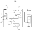
- FIG. 2 shows the second circuit configuration diagram in this embodiment. The description of the same points as the circuit configuration diagram of FIG. 1 will be omitted.
- the difference from FIG. 1 is that the reference voltage selection terminal 115 is connected to GND, and the input to the reference voltage Vref of the A/D converter 117 of the microcomputer 116 is not the output 106 of the regulator B103 but the regulator A102.
- the difference is that the output is 105 and the output 105 of the regulator A102 is not connected to the sensor 118.
- the reference voltage selection circuit 114 selects a voltage based on the internal power supply 104 and outputs it as the reference voltage 111 of the regulator A102.
- the internal power supply 104 does not have an output to the outside, it is not easily affected by disturbance unlike the output 106 of the regulator B103, which may fluctuate depending on the load conditions. Further, if the configuration of the internal power supply 104 is a circuit called a bandgap reference, it can be a voltage source that is extremely stable even in a temperature environment. In FIG. 2, by operating as a linear regulator with reference to such a stable voltage source, the regulator A102 has an absolute value as compared with the case of operating as a tracking regulator as shown in the circuit configuration diagram of FIG. It is possible to obtain a highly accurate voltage output.
- the output voltage value of the regulator A102 at this time is determined by the output voltage of the internal power supply 104 and the voltage division ratio of the voltage dividing resistor A107 and the voltage dividing resistor C113, and can be adjusted to a desired value.
- the sensor 118 in FIG. 2 is assumed to generate a sensor output by an electromotive force, such as a hall sensor or an optical sensor.
- an electromotive force such as a hall sensor or an optical sensor.
- the output of the sensor 118 does not depend on the power supply voltage of the sensor, it is detected as an absolute value. Therefore, in order for the microcomputer 116 to accurately A/D convert the output of the sensor 118, the input voltage to the reference voltage Vref of the A/D converter 117 is required to output a stable absolute value, and the regulator A102 is linear. By operating as a regulator, the output 105 can be input to the reference voltage Vref.
- the semiconductor integrated circuit 101 in this embodiment supplies a voltage to the first voltage regulator 102 that adjusts the output voltage based on the reference voltage and the external element.
- a second voltage regulator 103, a voltage source 104 having no output to the outside, and a selection circuit 114 for switching the reference voltage input to the first regulator 102 are provided, and the selection circuit 114 is the first voltage regulator 102.
- the selection circuit 114 operates so that the regulator A 102 functions as a tracking regulator when the input to the reference voltage selection terminal 115 is High and as a linear regulator when it is Low.
- the opposite may be true.
- FIGS. 1 and 2 an example in which the output of the sensor 118 is A / D converted by the microcomputer 116 is taken up, but in other cases where a tracking regulator is required, in order to prevent latch-up of the output destination element, There is a case where the timings of the voltage falling and rising of the two power supplies (or more) should not be mixed. Further, the disadvantages of the tracking regulator are that another regulator for producing the reference voltage is necessary, and if the regulator (regulator B103 in this embodiment) that is the source of the reference voltage fails, the output is disabled. is there.
- FIG. 3 is a circuit configuration diagram in the second embodiment.
- the configurations of the reference voltage input terminal 301 and the external regulator 302 are different from those in the first embodiment.
- the description of the configuration common to the first embodiment will be omitted.
- the output voltage of the external regulator 302 is input to the reference voltage input terminal 301, divided by the voltage dividing resistor B112, and input to the reference voltage selection circuit 114.
- the reference voltage 111 can be obtained from a regulator not inside the power supply IC 101, and the power supply IC 101 can be used in various ways. Increases the degree of freedom when applying to products.
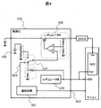
- FIG. 4 is a circuit configuration diagram in the third embodiment. This embodiment is different from the first embodiment in the configuration of the communication circuit 401, the communication signal input/output terminal 402, and the reference voltage selection signal 403. The description of the configuration common to the first or second embodiment will be omitted.
- the microcomputer 116 sends a command for specifying the voltage of the reference voltage 111 to the communication circuit 401 of the power supply IC 101 via the signal input terminal 402.
- the communication circuit 401 receives a command from the microcomputer and inputs the reference voltage selection signal 403 to the reference voltage selection circuit 114. For example, when the voltage based on the regulator B 103 is desired to be the reference voltage 111, High is input as the reference voltage selection signal, and when the internal power supply 104 is desired to be the reference voltage 111, Low is input as the reference voltage selection signal.
- the reference voltage selection circuit 114 selects the reference voltage 111 according to the value of the reference voltage selection signal 403 and inputs it to the regulator A 102.
- the output of the regulator A102 can be switched by a command from the microcomputer 116.
- the regulator A 102 when the regulator A 102 is operating as a tracking regulator and the microcomputer 116 detects an abnormality in the regulator B 103, the regulator A 102 is switched to the operation as a linear regulator so that the regulator A 102 operates in the same abnormal state. It is effective when you want to avoid becoming.
- the regulator A102 since the regulator A102 is used as the power supply for the sensor 118 having an output proportional to the power supply voltage as in FIG. 1 of the first embodiment, when the regulator A102 is used as a tracking regulator, the microcomputer 116 is the regulator A102. Is switched to operate as a linear regulator so that the output voltage is different from the output voltage of the tracking regulator, the output of the sensor 118 is intentionally changed, and the operation and accuracy of the A/D converter 117 is changed from the change amount. Can also be diagnosed.
- FIG. 5 is a circuit configuration diagram in the third embodiment. The description of the same configuration as that of the above-described embodiment will be omitted.
- the present embodiment is different from the first embodiment in that the failure detection circuit 501, the abnormal signal 502, the abnormal signal output terminal 503, the switch A 504, the switch B 505, the switch C 506, and the error input terminal 507 of the microcomputer 116 are configured. different.
- the abnormality detection circuit 501 monitors the output voltage of the regulator B 103. When the output voltage is within a certain normal range, the abnormality signal 502 is set to Low, and when the output voltage is out of the normal range, the abnormality signal 502 is set to High. Output.
- the abnormality signal 502 is input to the reference voltage selection circuit 114. Further, the abnormal signal 502 is output from the abnormal signal output terminal 503 to the outside of the power supply IC 101, and is input to the switch A504, the switch B505, the switch C506, and the abnormal signal input terminal 507 of the microcomputer 116.
- the reference voltage selection circuit 114 selects a voltage based on the output voltage of the regulator B103 and outputs it as the reference voltage 111.
- the reference voltage selection circuit 114 receives the signal and outputs a voltage based on the internal power supply 104 as a reference voltage 111.
- the voltage dividing resistor A107, the voltage dividing resistor B113, and the voltage dividing resistor C113 are adjusted so that the output voltage of the regulator A102 when operated as a linear regulator becomes the same as the output voltage when operated as a tracking regulator. It is assumed that
- the switch A 504, the switch B 505, and the switch C 506 are in a short circuit, open circuit, and short circuit state when the abnormality signal 502 is Low, and the output 106 of the regulator B 103 is connected to the VDD power supply of the microcomputer 116 and the A/D converter.
- the reference voltage Vref of 117 is input, and the output 105 of the regulator A 102 is input to the sensor 118.
- the switch A 504, the switch B 505, and the switch C 506 are switched to the open, short-circuited, and open states, respectively, the output 106 of the regulator B 103 is disconnected from the input to the microcomputer 116, and the output of the regulator A 102 of the sensor 118 is output.
- the microcomputer 116 starts processing for safely stopping the system.
- the regulator A 102 can be used as a backup power supply when the regulator B 103 has an abnormality, and prevents the microcomputer 116 from malfunctioning or being damaged due to an abnormal power supply voltage input. It is possible to perform processing for the safe stop of the controlled system.
- Such a mechanism is particularly effective for ensuring safety in the event of a failure of the power supply function in an electronic control unit in a field where high safety is required, such as braking and steering of an automobile and automatic driving.
Landscapes
- Engineering & Computer Science (AREA)
- Physics & Mathematics (AREA)
- Electromagnetism (AREA)
- General Physics & Mathematics (AREA)
- Radar, Positioning & Navigation (AREA)
- Automation & Control Theory (AREA)
- Continuous-Control Power Sources That Use Transistors (AREA)
Abstract
電源ASICを、異なる出力特性を持つレギュレータがそれぞれ必要な複数の製品に適用させようとする場合、それぞれを独立に設けると、一方の製品では、もう一方のためのレギュレータが不必要ということになり、無駄、コスト高となってしまうという課題があった。 本発明による半導体集積回路は、基準電圧に基づいて出力電圧を調整する第1の電圧レギュレータと、外部素子に電圧を供給する第2の電圧レギュレータと、外部への出力を持たない電圧源と、前記第1のレギュレータへ入力する前記基準電圧を切り替える選択回路を備え、前記選択回路は、前記基準電圧を、前記電圧源の出力に基づく第1の電圧と、前記第2の電圧レギュレータの出力に基づく第2の電圧とで切り替える。
Description
本発明は半導体集積回路に関する
特定の用途向けに開発される半導体集積回路であるASIC(Application Specific Integrated Circuit)は、対象の製品を絞ることで、必要な機能のみに最適化して搭載し、単価を下げる事が出来る。一方で、回路を個別に設計するための人件費や、高額な製造用のフォトマスクを試作品も含めて専用に作製することから、多くの開発費を必要とし、その結果、生産数量の大小が単価に大きな影響を与えるという課題もある。
この課題に対し、ASICに対し、最小限の工夫を加えることで機能に汎用性を持たせ、対象とする製品を広げて生産数を増やせば単価を下げることが出来る。例えば、電源ASICの場合は、搭載される製品が異なれば、出力電圧や精度をはじめとした特性への要求が製品毎に異なるが、それぞれの要求に対して全く個別の回路を搭載するのではなく、ピンや回路を可能な限り共有することで単価への影響を最小限とする事が出来る。例えば、特許文献1には、「簡便な方法でマイコンへの供給電源電圧を可変でき、同一の電源ICを多様なマイコンに適応可能な低コストの電子制御装置を実現する。ディスリート抵抗10の値を判定するためスイッチ21がオンし、電流源11からの電流値とディスクリート抵抗10の抵抗値に応じた電圧がIn1端子に発生する。AD変換器12によりIn1端子電圧がAD変換され選択的に接続されたディスクリート抵抗10に応じたデジタルコードが検出される。レジスタ13にはAD変換結果が保存され、AD変換器12によるディスクリート抵抗10の抵抗値判定が完了する。AD変換器12による抵抗値判定完了後に、各電源電圧V1、V2、V3が起動を開始する。コア電圧V3は、レジスタ13で設定された基準電圧14に応じた電圧で起動することで、所望の電源供給が完了する。」と記載されており、異なる電圧値の出力を単一のレギュレータで簡便に実現可能としている。
電源ASICを複数の製品に適用させようとしている場合、ある製品では、センサ電源をA/Dコンバータの基準電圧と一致させたり、電源電圧の立ち上がり、立下りのタイミングを他のレギュレータと一致させたりする目的で、他のレギュレータ電圧を基準に電圧を生成して、基準レギュレータの電圧変動に追従するトラッキングレギュレータが要求される場合がある。また、別のある製品では、高い精度が求められ、他のレギュレータの電圧変動に影響されることが望ましくないことから、基準の電圧をASIC内部の固定電圧とした一般的なリニアレギュレータ(以下、単にリニアレギュレータと呼ぶ)が必要となる場合がある。このように、異なる出力特性を持つレギュレータが必要となった場合に、それぞれを独立に設けると、一方の製品では、もう一方のためのレギュレータが不必要ということになり、無駄、コスト高となってしまうという課題があった。
本発明による半導体集積回路は、基準電圧に基づいて出力電圧を調整する第1の電圧レギュレータと、外部素子に電圧を供給する第2の電圧レギュレータと、外部への出力を持たない電圧源と、前記第1のレギュレータへ入力する前記基準電圧を切り替える選択回路を備え、前記選択回路は、前記基準電圧を、前記電圧源の出力に基づく第1の電圧と、前記第2の電圧レギュレータの出力に基づく第2の電圧とで切り替える。
本発明によれば、出力電圧を調整する電圧レギュレータ回路部分を共通として、電圧レギュレータ回路に入力する基準電圧を、他のレギュレータ出力と、ASIC内部の固定電圧とで切り替えるための回路を追加することで、トラッキングレギュレータ出力と、リニアレギュレータ出力の特性を両方実現可能となる。これにより、レギュレータ1CH分とほぼ変わらない実装面積で複数の製品からの異なる要求を満たすことが可能となり、ASICの単価を低減することが出来る。
図1、図2を用いて、本発明の実施例1について説明する。
図1は本実施例における1つ目の回路構成図を示したものである。
電源IC101はレギュレータA102と、レギュレータB103と、内部電源104を備えている。
レギュレータA102は外部への出力105を持ち、出力105の電圧を分圧抵抗A107で分圧して、エラーアンプ108の反転端子に入力している。エラーアンプ108の出力はNMOSFET109のゲートに接続されており、エラーアンプ108の反転端子への入力電圧と、非反転端子へ入力される基準電圧111の電圧が等しくなるよう、エラーアンプ108がNMOSFET109のソース-ドレイン間の電圧降下を調整し、電源IC101の電源入力端子110から入力される電源電圧から出力105を得ている。
レギュレータB103は、外部への出力106を持ち、内部電源104は外部への出力を持たない電圧源である。
レギュレータBの出力電圧と、内部電源104の出力電圧は、それぞれ電源IC101内に備えられた分圧抵抗B112、分圧抵抗C113で分圧され、基準電圧選択回路114に入力される。基準電圧選択回路は基準電圧選択端子115の入力値がHighの場合はレギュレータBの出力を分圧した電圧を、基準電圧選択端子115の入力がLowの場合は、内部電源104の出力を分圧した電圧を選択し、基準電圧111として、エラーアンプ108の非反転端子に入力する。
なお、基準電圧選択端子115を基板上でGND、もしくは5Vや3V等のHigh入力となる電圧に固定することによって、レギュレータA102は、電源IC101の起動直後から選択された特性の電圧を出力することが出来る。更に、基準電圧端子115を電源IC101内で抵抗を介してHighレベルにプルアップすれば、基準電圧選択端子115を基板上でオープンとしてするだけで基準電圧選択回路114はHigh入力を検出する。
図1に於いてはレギュレータA102の出力105は、基準電圧選択端子115に電圧源が接続され、Highを入力しているので、レギュレータBの出力106に従って出力105の電圧を調整するトラッキングレギュレータとして動作し、レギュレータBの出力106の電圧が外部負荷の影響等で変動した場合は、出力105の電圧も追従して変動する。
また、分圧抵抗A107、分圧抵抗B113の分圧比が等しければ、レギュレータA102とレギュレータB103の出力105、106は常に等しくなる。更に、分圧抵抗A107、分圧抵抗B113の分圧比を調整することで、レギュレータA102とレギュレータB103の出力105、106の電圧の比を調整することが可能であり、この時、出力105の電圧は出力106の電圧の変動に追従して、出力106の電圧と一定の比を保ちながら変動する。
なお、本実施例では、分圧抵抗A107、分圧抵抗B113の分圧比は同じものとする。
レギュレータA102の出力105はセンサ118へ電源として入力され、センサ118の出力はマイコン116のA/Dコンバータ117にアナログ入力値Vinとして接続されている。レギュレータB103の出力106はマイコン116のVDD電源及びA/Dコンバータへ基準電圧Vrefとして入力されている。
例えば、センサ118が、抵抗体の温度特性によって、センサ118の電源電圧である出力105を分圧した電圧の変動を温度変化として出力するなど、出力105の電圧値に比例する出力特性を持っている場合、センサ118の出力値をA/Dコンバータ117で精度よく変換するためには、A/Dコンバータの基準電圧VrefであるレギュレータB103の出力106と、レギュレータAの出力105の電圧値は常に同じである必要がある。前述の通り、本実施例では出力106と出力105は常に等しい電圧を出力するため、センサ118からのアナログ出力を精度よくA/Dコンバータ117で変換することが出来る。
図2は本実施例における2つ目の回路構成図を示したものである。図1の回路構成図と同じ点についての説明は省略する。図1との相違点は、基準電圧選択端子115がGNDに接続されている点、マイコン116のA/Dコンバータ117の基準電圧Vrefへの入力が、レギュレータB103の出力106ではなく、レギュレータA102の出力105である点、レギュレータA102の出力105がセンサ118へ接続されていない点が異なる。
図2では基準電圧端子115にLowが入力されていることになるため、基準電圧選択回路114は内部電源104を元にした電圧を選択してレギュレータA102の基準電圧111として出力する。
内部電源104は外部に出力を持たないため、負荷条件によって出力が変動するおそれのあるレギュレータB103の出力106とは異なり、外乱の影響を受けにくい。更に、内部電源104の構成をバンドギャップリファレンスと呼ばれる回路にすれば、温度環境に対しても非常に安定した電圧源とする事が出来る。図2に於いては、このような安定した電圧源を基準とするリニアレギュレータとして動作することにより、レギュレータA102は、図1の回路構成図の様にトラッキングレギュレータとして動作させた場合よりも絶対値として高精度な電圧出力を得る事が出来る。
尚、この時のレギュレータA102の出力電圧値は、内部電源104の出力電圧と、分圧抵抗A107、分圧抵抗C113の分圧比で決定され、所望の値に調整することが可能である。
図2におけるセンサ118は、ホールセンサや光センサの様に、起電力によってセンサ出力を発生させるものを想定している。この場合、センサ118の出力はセンサの電源電圧に依存しないため、絶対値として検出することになる。したがって、マイコン116がセンサ118の出力を精度よくA/D変換するためには、A/Dコンバータ117の基準電圧Vrefへの入力電圧は安定した絶対値の出力が必要であり、レギュレータA102をリニアレギュレータとして動作させることで、出力105を基準電圧Vrefへの入力が得られる。
以上、図1、図2を用いて示したように、本実施例における半導体集積回路101は、基準電圧に基づいて出力電圧を調整する第1の電圧レギュレータ102と、外部素子に電圧を供給する第2の電圧レギュレータ103と、外部への出力を持たない電圧源104と、第1のレギュレータ102へ入力する基準電圧を切り替える選択回路114を備え、選択回路114は、第1の電圧レギュレータ102の基準電圧を電圧源104の出力に基づく第1の電圧と第2の電圧レギュレータ103の出力に基づく第2の電圧とで切り替えるようにすることで、レギュレータA102(第1のレギュレータ)の出力の特性をトラッキングレギュレータとリニアレギュレータとで切り替える事が出来る。そのため、電源IC101を複数の製品に搭載する際に、それぞれの製品で異なる特性のレギュレータ出力を求められる場合に於いても、レギュレータA102の出力特性を切り替えることで可能になる。なお、本実施例では、基準電圧選択端子115への入力がHighの場合にはトラッキングレギュレータとして、Lowの場合にはリニアレギュレータとしてレギュレータA102が機能するように選択回路114が動作する例を示したが、逆であってもよい。
図1、図2ではセンサ118の出力をマイコン116でA/D変換する例を取り上げたが、その他にも、トラッキングレギュレータが必要とされる場合として、出力先素子のラッチアップ防止のために、2電源(もしくはそれ以上)の電圧立下りと立ち上がりのタイミングを前後させてはいけない場合が挙げられる。また、トラッキングレギュレータのデメリットとしては、基準電圧を作るための別のレギュレータが必要な点や、基準電圧の元になるレギュレータ(本実施例ではレギュレータB103)が故障した場合に出力不能となる点がある。そのため、リニアレギュレータが必要とされる場合として、前述のような高精度な電圧値を求められる場合に加え、冗長系の電源等、他のレギュレータと同時に故障して欲しくない場合がある。更に、リニアレギュレータの基準電圧に利用する電圧(本実施例では内部電源104)は、電源IC101内の各所に分配されている内部基準電圧を利用する事が出来る。そのため、精度や冗長性は求められないが、単純にトラッキングレギュレータとして動作させる場合とは別の電圧レベルが求められる場合にも、リニアレギュレータとしての動作と切り替えた方が、他のレギュレータの出力を利用するよりも、簡便な回路、配線の構成とする事が出来る。
図3は第2の実施例における回路構成図である。本実施例は基準電圧入力端子301と外部レギュレータ302の構成が第1の実施例とは異なる。なお、第1の実施例と共通する構成については、説明を省略する。
本実施例では、外部レギュレータ302の出力電圧が基準電圧入力端子301に入力され、分圧抵抗B112で分圧されて基準電圧選択回路114へ入力されている。
このように、基準電圧入力端301を設けることにより、レギュレータA101をトラッキングレギュレータとして動作させる際に、電源IC101の内部に無いレギュレータから基準電圧111を得る事が出来るようになり、電源IC101を多様な製品へ適用する際の自由度が向上する。
図4は第3の実施例に於ける回路構成図である。本実施例は通信回路401と、通信信号入出力端子402と基準電圧選択信号403の構成が第1の実施例とは異なる。なお、第1または第2の実施例と共通する構成については、説明を省略する。
マイコン116は信号入力端子402を介して電源IC101の通信回路401に基準電圧111の電圧を指定する指令を送信する。通信回路401はマイコンからの指令を受信して、基準電圧選択信号403を基準電圧選択回路114に入力する。例えば、レギュレータB103を基にした電圧を基準電圧111としたい場合は、基準電圧選択信号としてHighを入力し、内部電源104を基準電圧111としたい場合は、基準電圧選択信号としてLowを入力する。
基準電圧選択回路114は基準電圧選択信号403の値に従って、基準電圧111を選択し、レギュレータA102に入力する。
これにより、レギュレータA102の出力は、マイコン116からの指令により切り替えることが可能となる。
本実施例は、例えば、レギュレータA102がトラッキングレギュレータとして動作していて、且つ、レギュレータB103の異常をマイコン116が検出した場合にレギュレータA102をリニアレギュレータとしての動作に切り替えることでレギュレータB103と同じ異常状態となるのを回避したい場合に有効である。また、他の例として、レギュレータA102を実施例1の図1と同様に電源電圧に比例する出力を持つセンサ118の電源とするため、トラッキングレギュレータとして使用している場合に、マイコン116がレギュレータA102をトラッキングレギュレータとしての出力電圧とは異なる出力電圧となるように、リニアレギュレータとして動作するよう切り替えることで、センサ118の出力を故意に変化させ、その変化量からA/Dコンバータ117の動作や精度を診断することも出来る。
図5は第3の実施例における回路構成図である。なお、前述した実施例と同様の構成については説明を省略する。本実施例は、故障検出回路501と、異常信号502と、異常信号出力端子503と、スイッチA504、スイッチB505、スイッチC506と、マイコン116のエラー入力端子507の構成が第1の実施例とは異なる。
異常検出回路501は、レギュレータB103の出力電圧をモニタしており、出力電圧がある正常範囲内にある場合は、異常信号502をLowとして、正常範囲を外れた場合には異常信号502をHighとして出力する。異常信号502は基準電圧選択回路114に入力される。更に、異常信号502は異常信号出力端子503から電源IC101の外部へ出力され、スイッチA504、スイッチB505、スイッチC506とマイコン116の異常信号入力端子507に入力される。
基準電圧選択回路114は異常信号502がLowの場合には、レギュレータB103の出力電圧を基にした電圧を選択して基準電圧111として出力する。異常信号502がHighになると、基準電圧選択回路114はその信号を受けて内部電源104を基にした電圧を基準電圧111として出力する。なお、リニアレギュレータとして動作させた時のレギュレータA102の出力電圧は、トラッキングレギュレータとして動作させた時の出力電圧と同じとなるよう、分圧抵抗A107、分圧抵抗B113、分圧抵抗C113を調整しているものとする。
スイッチA504、スイッチB505、スイッチC506は、それぞれ、異常信号502がLowの場合には、短絡、開放、短絡の状態となっており、レギュレータB103の出力106をマイコン116のVDD電源とA/Dコンバータ117の基準電圧Vrefに入力し、レギュレータA102の出力105をセンサ118に入力する。異常信号502がHighになると、スイッチA504、スイッチB505、スイッチC506はそれぞれ開放、短絡、開放の状態に切り替わり、レギュレータB103の出力106をマイコン116への入力から切り離し、レギュレータA102の出力をセンサ118の入力から切り離してマイコン116のVDD電源に入力する。これにより、レギュレータB103の異常時にマイコン116の電源入力をレギュレータA102の出力105に切り替えることによって、マイコン116の誤動作や破壊を防ぐ事が出来る。
マイコン116は異常信号入力端子507から異常信号Highが入力されると、安全にシステムを停止させるための処理を開始する。
以上の様に、本実施例によれば、レギュレータB103の異常発生時に、バックアップ電源としてレギュレータA102を用いる事が出来、異常な電源電圧の入力によるマイコン116の誤動作や破壊を防ぎ、更にマイコン116が制御するシステムの安全な停止のための処理を行う事が出来る。こういった仕組みは、例えば、自動車のブレーキやステアリング、自動運転等、高い安全性が求められる分野における電子制御装置において、電源機能の故障時の安全を担保するために特に有効である。
101 電源IC
102 レギュレータA
103 レギュレータB
104 内部電源
105 レギュレータA出力
106 レギュレータB出力
107 分圧抵抗A
108 エラーアンプ
109 NMOSFET
110 電源入力端子
111 基準電圧
112 分圧抵抗B
113 分圧抵抗C
114 基準電圧選択回路
115 基準電圧選択端子
116 マイコン
117 A/Dコンバータ
118 センサ
301 基準電圧入力端子
302 外部レギュレータ
401 通信回路
402 通信信号入出力端子
403 基準電圧選択信号
501 異常検出回路
502 異常信号
503 異常信号出力端子
504 スイッチA
505 スイッチB
506 スイッチC
507 異常信号入力端子
Claims (6)
- 基準電圧に基づいて出力電圧を調整する第1の電圧レギュレータと、外部素子に電圧を供給する第2の電圧レギュレータと、外部への出力を持たない電圧源と、前記第1のレギュレータへ入力する前記基準電圧を切り替える選択回路を備え、
前記選択回路は、前記基準電圧を、前記電圧源の出力に基づく第1の電圧と、前記第2の電圧レギュレータの出力に基づく第2の電圧とで切り替える半導体集積回路。 - 基準電圧に基づいて出力電圧を調整する第1の電圧レギュレータと、外部からの電圧を入力値とする基準電圧入力端子と、外部への出力を持たない電圧源と、前記第1のレギュレータへ入力する前記基準電圧を切り替える選択回路を備え、
前記選択回路は、前記基準電圧を、前記電圧源の出力に基づく第1の電圧と、前記基準電圧入力端子からの入力電圧に基づく第2の電圧とで切り替える半導体集積回路。 - 基準電圧選択端子を備え、
前記選択回路は、前記基準電圧選択端子に前記半導体集積回路の外部から入力される信号に基づいて前記基準電圧を選択する請求項1または第2に記載の半導体集積回路。 - 外部との通信部を備え、
前記通信部を介して入力される信号に基づいて前記選択回路が前記基準電圧を選択する請求項1または2に記載の半導体集積回路。 - 前記第2のレギュレータの異常を検出する異常検出部を備え、
前記異常検出部が前記第2のレギュレータの異常を検出した場合、前記選択回路は前記第1の電圧レギュレータの基準電圧を前記第1の電圧に切り替える請求項1乃至4の何れかに記載の半導体集積回路。 - 請求項1乃至5の何れかに記載の半導体集積回路と、前記半導体集積回路から電圧が供給されるマイコンと、を備える電子制御装置
Priority Applications (1)
| Application Number | Priority Date | Filing Date | Title |
|---|---|---|---|
| JP2021503450A JP7032605B2 (ja) | 2019-03-01 | 2020-01-21 | 半導体集積回路 |
Applications Claiming Priority (2)
| Application Number | Priority Date | Filing Date | Title |
|---|---|---|---|
| JP2019037154 | 2019-03-01 | ||
| JP2019-037154 | 2019-03-01 |
Publications (1)
| Publication Number | Publication Date |
|---|---|
| WO2020179250A1 true WO2020179250A1 (ja) | 2020-09-10 |
Family
ID=72337951
Family Applications (1)
| Application Number | Title | Priority Date | Filing Date |
|---|---|---|---|
| PCT/JP2020/001810 Ceased WO2020179250A1 (ja) | 2019-03-01 | 2020-01-21 | 半導体集積回路 |
Country Status (2)
| Country | Link |
|---|---|
| JP (1) | JP7032605B2 (ja) |
| WO (1) | WO2020179250A1 (ja) |
Cited By (1)
| Publication number | Priority date | Publication date | Assignee | Title |
|---|---|---|---|---|
| WO2022208933A1 (ja) * | 2021-03-30 | 2022-10-06 | 日立Astemo株式会社 | 半導体装置、変速機の制御装置、電子制御装置の制御方法 |
Citations (5)
| Publication number | Priority date | Publication date | Assignee | Title |
|---|---|---|---|---|
| JPH02130010U (ja) * | 1989-04-03 | 1990-10-26 | ||
| JPH06168038A (ja) * | 1992-12-01 | 1994-06-14 | Fujitsu Ltd | 電源供給装置 |
| JPH11353040A (ja) * | 1998-04-10 | 1999-12-24 | Matsushita Electric Ind Co Ltd | 電源装置 |
| JP2003330553A (ja) * | 2002-05-15 | 2003-11-21 | Matsushita Electric Ind Co Ltd | 電源回路および電源装置 |
| JP2006018409A (ja) * | 2004-06-30 | 2006-01-19 | Denso Corp | 電源回路 |
-
2020
- 2020-01-21 WO PCT/JP2020/001810 patent/WO2020179250A1/ja not_active Ceased
- 2020-01-21 JP JP2021503450A patent/JP7032605B2/ja active Active
Patent Citations (5)
| Publication number | Priority date | Publication date | Assignee | Title |
|---|---|---|---|---|
| JPH02130010U (ja) * | 1989-04-03 | 1990-10-26 | ||
| JPH06168038A (ja) * | 1992-12-01 | 1994-06-14 | Fujitsu Ltd | 電源供給装置 |
| JPH11353040A (ja) * | 1998-04-10 | 1999-12-24 | Matsushita Electric Ind Co Ltd | 電源装置 |
| JP2003330553A (ja) * | 2002-05-15 | 2003-11-21 | Matsushita Electric Ind Co Ltd | 電源回路および電源装置 |
| JP2006018409A (ja) * | 2004-06-30 | 2006-01-19 | Denso Corp | 電源回路 |
Cited By (4)
| Publication number | Priority date | Publication date | Assignee | Title |
|---|---|---|---|---|
| WO2022208933A1 (ja) * | 2021-03-30 | 2022-10-06 | 日立Astemo株式会社 | 半導体装置、変速機の制御装置、電子制御装置の制御方法 |
| CN116982017A (zh) * | 2021-03-30 | 2023-10-31 | 日立安斯泰莫株式会社 | 半导体装置、变速器的控制装置、电子控制装置的控制方法 |
| JP7498852B2 (ja) | 2021-03-30 | 2024-06-12 | 日立Astemo株式会社 | 半導体装置、変速機の制御装置、電子制御装置の制御方法 |
| US12462960B2 (en) | 2021-03-30 | 2025-11-04 | Hitachi Astemo, Ltd. | Semiconductor device, control device for transmission, and control method of electronic control unit |
Also Published As
| Publication number | Publication date |
|---|---|
| JP7032605B2 (ja) | 2022-03-08 |
| JPWO2020179250A1 (ja) | 2021-10-14 |
Similar Documents
| Publication | Publication Date | Title |
|---|---|---|
| JP5093037B2 (ja) | 負荷駆動回路 | |
| KR102019812B1 (ko) | 전압 레귤레이터 | |
| US10831222B2 (en) | Semiconductor apparatus for power supply control and output voltage variable power supply apparatus | |
| US10761549B2 (en) | Voltage sensing mechanism to minimize short-to-ground current for low drop-out and bypass mode regulators | |
| US10185338B1 (en) | Digital low drop-out (LDO) voltage regulator with analog-assisted dynamic reference correction | |
| JP7534598B2 (ja) | 電源装置および電源制御用半導体装置 | |
| JP5987819B2 (ja) | 電源装置 | |
| JP7032605B2 (ja) | 半導体集積回路 | |
| US7622901B2 (en) | System power supply apparatus and operational control method | |
| SE469732B (sv) | Analog anpassningsenhet | |
| JP4461817B2 (ja) | 半導体集積回路装置 | |
| US7619396B2 (en) | Thermal dissipation improved power supply arrangement and control method thereof | |
| JP7170935B2 (ja) | 電源装置及び電子機器 | |
| US7663470B2 (en) | Trimming circuit and electronic circuit | |
| JP4619866B2 (ja) | 定電圧電源回路及び定電圧電源回路の動作制御方法 | |
| US8957646B2 (en) | Constant voltage circuit and electronic device including same | |
| KR102058486B1 (ko) | 복수의 전원 공급 유닛 간의 부하 분담 조절용 오프셋 회로를 가지는 부하 분담 컨트롤러 및 병렬 구성 전원 공급 시스템 | |
| JP2022148990A (ja) | シャントレギュレータ | |
| EP1882308B1 (en) | Integrated driver circuit structure | |
| JP7678287B2 (ja) | 半導体集積回路 | |
| US12578746B2 (en) | Voltage regulator and semiconductor device | |
| JP7658059B2 (ja) | システムおよび火災報知器 | |
| US20250158527A1 (en) | Current output device | |
| US7746019B2 (en) | Servo control circuit | |
| JP2005100295A (ja) | サーマルシャットダウン回路 |
Legal Events
| Date | Code | Title | Description |
|---|---|---|---|
| 121 | Ep: the epo has been informed by wipo that ep was designated in this application |
Ref document number: 20767447 Country of ref document: EP Kind code of ref document: A1 |
|
| ENP | Entry into the national phase |
Ref document number: 2021503450 Country of ref document: JP Kind code of ref document: A |
|
| NENP | Non-entry into the national phase |
Ref country code: DE |
|
| 122 | Ep: pct application non-entry in european phase |
Ref document number: 20767447 Country of ref document: EP Kind code of ref document: A1 |