WO2020175747A1 - 복수의 표준 cmos 센서를 에너지 효율적으로 집적하는 센서 회로 및 이를 포함하는 센서 장치 - Google Patents
복수의 표준 cmos 센서를 에너지 효율적으로 집적하는 센서 회로 및 이를 포함하는 센서 장치 Download PDFInfo
- Publication number
- WO2020175747A1 WO2020175747A1 PCT/KR2019/007063 KR2019007063W WO2020175747A1 WO 2020175747 A1 WO2020175747 A1 WO 2020175747A1 KR 2019007063 W KR2019007063 W KR 2019007063W WO 2020175747 A1 WO2020175747 A1 WO 2020175747A1
- Authority
- WO
- WIPO (PCT)
- Prior art keywords
- capacitor
- switch
- output
- integrator
- sensor
- Prior art date
- Legal status (The legal status is an assumption and is not a legal conclusion. Google has not performed a legal analysis and makes no representation as to the accuracy of the status listed.)
- Ceased
Links
Images


Classifications
-
- H—ELECTRICITY
- H04—ELECTRIC COMMUNICATION TECHNIQUE
- H04N—PICTORIAL COMMUNICATION, e.g. TELEVISION
- H04N25/00—Circuitry of solid-state image sensors [SSIS]; Control thereof
- H04N25/70—SSIS architectures; Circuits associated therewith
- H04N25/79—Arrangements of circuitry being divided between different or multiple substrates, chips or circuit boards, e.g. stacked image sensors
-
- G—PHYSICS
- G01—MEASURING; TESTING
- G01L—MEASURING FORCE, STRESS, TORQUE, WORK, MECHANICAL POWER, MECHANICAL EFFICIENCY, OR FLUID PRESSURE
- G01L9/00—Measuring steady of quasi-steady pressure of fluid or fluent solid material by electric or magnetic pressure-sensitive elements; Transmitting or indicating the displacement of mechanical pressure-sensitive elements, used to measure the steady or quasi-steady pressure of a fluid or fluent solid material, by electric or magnetic means
- G01L9/12—Measuring steady of quasi-steady pressure of fluid or fluent solid material by electric or magnetic pressure-sensitive elements; Transmitting or indicating the displacement of mechanical pressure-sensitive elements, used to measure the steady or quasi-steady pressure of a fluid or fluent solid material, by electric or magnetic means by making use of variations in capacitance, i.e. electric circuits therefor
- G01L9/125—Measuring steady of quasi-steady pressure of fluid or fluent solid material by electric or magnetic pressure-sensitive elements; Transmitting or indicating the displacement of mechanical pressure-sensitive elements, used to measure the steady or quasi-steady pressure of a fluid or fluent solid material, by electric or magnetic means by making use of variations in capacitance, i.e. electric circuits therefor with temperature compensating means
-
- G—PHYSICS
- G01—MEASURING; TESTING
- G01P—MEASURING LINEAR OR ANGULAR SPEED, ACCELERATION, DECELERATION, OR SHOCK; INDICATING PRESENCE, ABSENCE, OR DIRECTION, OF MOVEMENT
- G01P15/00—Measuring acceleration; Measuring deceleration; Measuring shock, i.e. sudden change of acceleration
- G01P15/02—Measuring acceleration; Measuring deceleration; Measuring shock, i.e. sudden change of acceleration by making use of inertia forces using solid seismic masses
- G01P15/08—Measuring acceleration; Measuring deceleration; Measuring shock, i.e. sudden change of acceleration by making use of inertia forces using solid seismic masses with conversion into electric or magnetic values
- G01P15/125—Measuring acceleration; Measuring deceleration; Measuring shock, i.e. sudden change of acceleration by making use of inertia forces using solid seismic masses with conversion into electric or magnetic values by capacitive pick-up
-
- G—PHYSICS
- G01—MEASURING; TESTING
- G01L—MEASURING FORCE, STRESS, TORQUE, WORK, MECHANICAL POWER, MECHANICAL EFFICIENCY, OR FLUID PRESSURE
- G01L9/00—Measuring steady of quasi-steady pressure of fluid or fluent solid material by electric or magnetic pressure-sensitive elements; Transmitting or indicating the displacement of mechanical pressure-sensitive elements, used to measure the steady or quasi-steady pressure of a fluid or fluent solid material, by electric or magnetic means
- G01L9/12—Measuring steady of quasi-steady pressure of fluid or fluent solid material by electric or magnetic pressure-sensitive elements; Transmitting or indicating the displacement of mechanical pressure-sensitive elements, used to measure the steady or quasi-steady pressure of a fluid or fluent solid material, by electric or magnetic means by making use of variations in capacitance, i.e. electric circuits therefor
-
- G—PHYSICS
- G01—MEASURING; TESTING
- G01N—INVESTIGATING OR ANALYSING MATERIALS BY DETERMINING THEIR CHEMICAL OR PHYSICAL PROPERTIES
- G01N27/00—Investigating or analysing materials by the use of electric, electrochemical, or magnetic means
- G01N27/02—Investigating or analysing materials by the use of electric, electrochemical, or magnetic means by investigating impedance
- G01N27/22—Investigating or analysing materials by the use of electric, electrochemical, or magnetic means by investigating impedance by investigating capacitance
- G01N27/223—Investigating or analysing materials by the use of electric, electrochemical, or magnetic means by investigating impedance by investigating capacitance for determining moisture content, e.g. humidity
-
- G—PHYSICS
- G01—MEASURING; TESTING
- G01N—INVESTIGATING OR ANALYSING MATERIALS BY DETERMINING THEIR CHEMICAL OR PHYSICAL PROPERTIES
- G01N27/00—Investigating or analysing materials by the use of electric, electrochemical, or magnetic means
- G01N27/02—Investigating or analysing materials by the use of electric, electrochemical, or magnetic means by investigating impedance
- G01N27/22—Investigating or analysing materials by the use of electric, electrochemical, or magnetic means by investigating impedance by investigating capacitance
- G01N27/223—Investigating or analysing materials by the use of electric, electrochemical, or magnetic means by investigating impedance by investigating capacitance for determining moisture content, e.g. humidity
- G01N27/225—Investigating or analysing materials by the use of electric, electrochemical, or magnetic means by investigating impedance by investigating capacitance for determining moisture content, e.g. humidity by using hygroscopic materials
-
- H—ELECTRICITY
- H04—ELECTRIC COMMUNICATION TECHNIQUE
- H04N—PICTORIAL COMMUNICATION, e.g. TELEVISION
- H04N25/00—Circuitry of solid-state image sensors [SSIS]; Control thereof
- H04N25/70—SSIS architectures; Circuits associated therewith
-
- H—ELECTRICITY
- H04—ELECTRIC COMMUNICATION TECHNIQUE
- H04N—PICTORIAL COMMUNICATION, e.g. TELEVISION
- H04N25/00—Circuitry of solid-state image sensors [SSIS]; Control thereof
- H04N25/70—SSIS architectures; Circuits associated therewith
- H04N25/76—Addressed sensors, e.g. MOS or CMOS sensors
-
- G—PHYSICS
- G01—MEASURING; TESTING
- G01P—MEASURING LINEAR OR ANGULAR SPEED, ACCELERATION, DECELERATION, OR SHOCK; INDICATING PRESENCE, ABSENCE, OR DIRECTION, OF MOVEMENT
- G01P15/00—Measuring acceleration; Measuring deceleration; Measuring shock, i.e. sudden change of acceleration
- G01P15/02—Measuring acceleration; Measuring deceleration; Measuring shock, i.e. sudden change of acceleration by making use of inertia forces using solid seismic masses
- G01P15/08—Measuring acceleration; Measuring deceleration; Measuring shock, i.e. sudden change of acceleration by making use of inertia forces using solid seismic masses with conversion into electric or magnetic values
- G01P2015/0862—Measuring acceleration; Measuring deceleration; Measuring shock, i.e. sudden change of acceleration by making use of inertia forces using solid seismic masses with conversion into electric or magnetic values being provided with particular means being integrated into a MEMS accelerometer structure for providing particular additional functionalities to those of a spring mass system
- G01P2015/0865—Measuring acceleration; Measuring deceleration; Measuring shock, i.e. sudden change of acceleration by making use of inertia forces using solid seismic masses with conversion into electric or magnetic values being provided with particular means being integrated into a MEMS accelerometer structure for providing particular additional functionalities to those of a spring mass system using integrated signal processing circuitry
Definitions
- the present invention relates to a sensor circuit and a sensor device including the same, and more particularly, in a sensor circuit capable of sensing environmental information of a circuit block installed in a semiconductor memory device, etc., a plurality of sensors such as pressure, humidity, and acceleration sensors. It relates to a sensor circuit for defining a standard CMOS sensor, integrating and reading energy efficiently, and a sensor device including the same.
- semiconductor memory devices etc.
- CMOS Complementary Metal Oxide Semiconductor
- sensors such as acceleration sensors, temperature sensors, pressure sensors, and image sensors are used in smart phones, and about 200 sensors are used in smart cars. As such, as sensors are expanded to the core parts of most devices, securing the competitiveness of the sensor industry is becoming an essential factor in strengthening national industrial competitiveness.
- the present invention has been proposed to solve the above-described conventional problem, and a sensor that adopts a dual quantization capacitance-digital converter structure to more accurately sense various environmental information such as pressure, humidity, acceleration, etc. and to reduce quantization noise simply.
- An object thereof is to provide a circuit and a sensor device.
- the present invention uses a paradigm of a standard CMOS sensor to provide energy to a plurality of standard CMOS sensors enabling the development of a high-performance, low-cost sensor system-on-chip (SoC) for measuring various environmental variables.
- An object of the present invention is to provide a sensor circuit efficiently integrated and a sensor device including the same.
- the environmental information sensor circuit is an environmental information sensor circuit including at least one of pressure information, humidity information, and acceleration information, and is a non-overlapping first clock signal. And a switch capacitor configured to output one of the pressure information, humidity information, and acceleration information based on a second clock signal.
- Single bit 1 including an integrator that integrates the output of the switch capacitor and outputs an analog value, and a single bit quantizer that compares the output of the integrator with a preset threshold voltage and outputs a digital signal of a single bit corresponding to the comparison result Car delta sigma converter; And a multi-bit quantizer connected to the output terminal of the integrator via a sampling switch, and quantizes the output of the integrator at a time point when the sampling switch is turned on according to a sampling signal.
- the switch capacitor is a second switch having one end connected to a power supply terminal and the other end and one end connected to a ground terminal of the first switch turned on/off by the second clock signal and turned on/off by the first clock signal
- a sensor capacitor connected to the other end of the device; One end is connected to the power terminal, the other end of the third switch turned on/off by the second clock signal, and one end connected to the ground terminal, and connected to the other end of the fourth switch turned on/off by the first clock signal.
- a capacitor for providing a reference voltage One end is connected to the power terminal, the other end of the fifth switch turned on/off by the second clock signal, and one end connected to the ground terminal, and connected to the other end of the sixth switch turned on/off by the first clock signal.
- a charge providing capacitor unit including the charge providing capacitor and the seventh switch may be provided, and the charge providing capacitor unit may be connected to the sensor capacitor and the reference voltage providing capacitor in a parallel structure.
- the single bit digital signal may be converted into an analog signal and applied to the seventh switch.
- the sensor capacitor is composed of a capacitor for a pressure sensor or a capacitor for a humidity sensor including a metal structure forming a space for forming a specific dielectric constant, and the metal structure is a first in the form of a shift formed continuously from one point. 1 metal structure; And a second metal structure in the form of a displacement that is continuously formed from a point different from one point of the first metal structure and is formed to be spaced apart from the first metal structure by a predetermined distance. Including, the first metal Each of the structure and the second metal structure may include a protrusion protruding upward.
- the number of the protrusions is N> b/(2 a ⁇ 36.4ppm ⁇ c ⁇ o ⁇ (A/d) ⁇ 1.3)
- N is the number of protrusions
- a is the number of effective bits of the double quantization capacitance digital converter
- b is the input capacitance area of the double quantization capacitance digital converter
- c is the resolution
- ⁇ 0 is the vacuum permittivity
- ⁇ r is the relative permittivity
- A May be the area (height * length) and d is the distance between protrusions).
- the first metal structure and the second metal structure may form a comb-shaped meshed structure exposed to air.
- the sensor capacitor is composed of an acceleration sensor capacitor, the acceleration sensor capacitor includes three bond wires installed to be spaced apart from each other on the upper surface of the base, and the left and right sides of the three bond wires excluding the bond wire in the middle Of the bond wire, each of both ends is fixedly connected to the upper surface of the base, one end of the intermediate bond wire is fixedly connected to the upper surface of the base, and the other end is separated apart from the base, and the intermediate bond wire A proof mass may be attached to the end of the other end of the.
- the integrator includes an OP amplifier and an integrated capacitor, an inverting input terminal of the OP amplifier is connected to an output terminal of the switch capacitor, and a non-inverting input terminal of the OP amplifier is connected to an output terminal of the switch capacitor through an eighth switch.
- the eighth switch and the non-inverting input terminal are connected to a reference voltage terminal (V Com ), and the integrated capacitor is inserted between the inverting input terminal and the output terminal of the OP amplifier via a ninth switch, and the The eighth switch may be controlled by the first clock signal, and the ninth switch may be controlled by the second clock signal.
- the integrator can output a current integral value.
- the multi-bit quantizer may be configured with a 7-bit synchronous SAR-ADC.
- the environmental information measuring apparatus includes the pressure information and humidity information based on the non-overlapping first and second clock signals, and A switch capacitor that outputs one of acceleration information;
- Single bit 1 including an integrator that integrates the output of the switch capacitor and outputs an analog value, and a single bit quantizer that compares the output of the integrator with a preset threshold voltage and outputs a digital signal of a single bit corresponding to the comparison result Car delta sigma converter;
- a multi-bit quantizer connected to the output terminal of the integrator via a sampling switch, and quantizes the output of the integrator at a time point when the sampling switch is turned on according to a sampling signal.
- a CMOS semiconductor can be used as a standard CMOS sensor as a new paradigm that views a CMOS semiconductor as a sensing element rather than a computation element, which uses a new non-ideality in which the characteristics of the CMOS semiconductor change due to changes in the external environment.
- CMOS integrated circuit CMOS integrated circuit
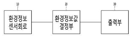
- FIG. 1 is a block diagram showing the configuration of an apparatus for measuring environmental information according to an embodiment of the present invention.
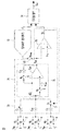
- FIG. 2 is a circuit conceptual diagram illustrating a basic configuration of an environmental information sensor circuit according to an embodiment of the present invention.
- FIG. 3 to 6 are diagrams for explaining a configuration in a case where the sensor capacitor shown in FIG. 2 is a pressure sensor capacitor.
- FIG. 7 and 8 are diagrams for explaining a configuration when the sensor capacitor shown in FIG. 2 is a humidity sensor capacitor.
- FIG. 9 is a diagram for explaining a configuration when the sensor capacitor shown in FIG. 2 is an acceleration sensor capacitor.
- FIG. 10 is a signal waveform diagram used to describe a single-bit first-order delta sigma path in the environmental information sensor circuit shown in FIG. 2.
- FIG. 11 is a signal waveform diagram used to describe a multi-bit quantizer in the environmental information sensor circuit shown in FIG. 2.
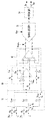
- FIG. 12 is a circuit conceptual diagram for explaining the configuration of an environmental information sensor circuit according to another embodiment of the present invention.
- FIG. 1 is a block diagram showing the configuration of an apparatus for measuring environmental information according to an embodiment of the present invention.
- the environmental information may include one or more of pressure information, humidity information, and acceleration information.
- the apparatus for measuring environment information may sense and output environment information (eg, one or more of pressure information, humidity information, and acceleration information).
- the apparatus for measuring environmental information measures at least one of pressure information, humidity information, and acceleration information based on a voltage output value that varies according to a change in the dielectric constant of a capacitor for measuring environmental information according to environmental changes, and measures The value can be output to other devices or devices connected to the environmental information measuring device.
- An environmental information measuring apparatus includes an environmental information sensor circuit 10, an environmental information value determining unit 20, and an output unit 30.
- the environment information sensor circuit 10 senses a change in external environment information and outputs the sensed value.
- the environmental information sensor circuit 10 has a wide input capacitance range (e.g., >10pF) and high resolution (e.g., ⁇ 1fF), and includes a single-bit first-order delta sigma converter and a multi-bit quantizer to increase energy efficiency. I can.
- the environmental information sensor circuit 10 may be considered to include a pressure sensor, a humidity sensor, and an acceleration sensor.
- an on-chip temperature sensor may be additionally installed to compensate for temperature/humidity using a look up table.
- the environment information value determination unit 20 determines an environment information value corresponding to a sensing signal output from the environment information sensor circuit 10.
- the output unit 30 outputs the environment information value determined by the environment information value determination unit 20.
- the environment information value output from the output unit 30 may be converted into a predetermined format and transmitted to another module that controls environment information, or may be transmitted to a video or audio output device to be converted and output into video or audio data.
- FIG. 2 is a circuit conceptual diagram illustrating a basic configuration of an environmental information sensor circuit according to an embodiment of the present invention.
- the environmental information sensor circuit 10 may include a switch capacitor 70, a single bit first order delta sigma converter 71, a multi bit quantizer 73, and a digital filter 74.
- the single-bit first order delta sigma converter 71, the multi-bit quantizer 73, and the digital filter 74 may be collectively referred to as a double quantization capacitance digital converter (CDC).
- CDC double quantization capacitance digital converter
- the switch capacitor 70 is switched by the non-overlapping clock signals ⁇ 1 and ⁇ 2 to output a predetermined charge charge ⁇ Q.
- the clock signal ⁇ 1 may be referred to as a first clock signal
- the clock signal ⁇ 2 may be referred to as a second clock signal.
- the switch capacitor 70 has one end connected to the power terminal V DD and the other end of the first switch 1 turned on/off by a second clock signal ⁇ 2, and one end connected to the ground terminal, and the first A sensor capacitor (C S ), one end connected to the node to which the other end of the second switch 2 is connected, which is turned on/off by the clock signal ⁇ 1, is connected to the power terminal (V DD ), and the second clock signal
- the other end of the third switch 3, which is turned on/off by ( ⁇ 2), and the other end of the fourth switch 4, which is connected to the ground terminal and turned on/off by the first clock signal ⁇ 1, are connected.
- the sensor capacitor (C S ), the reference voltage providing capacitor (C Ref ), and the charge providing capacitor (C Q ) are connected in parallel, but the charge providing capacitor (C Q ) is the seventh switch (7) It is connected in parallel with the sensor capacitor (C S ) and the reference voltage supply capacitor (C Ref ) via.
- a charge providing capacitor unit including the charge providing capacitor C Q and the seventh switch 7 may be provided, and the charge providing capacitor unit may be provided with the sensor capacitor C S and the reference voltage It can be connected to the providing capacitor (C Ref ) in a parallel structure.
- the output ( ⁇ Q) from the switch capacitor 70 will be (C S -C Ref -b s ⁇ C Q ) ⁇ V DD .
- the density ( ⁇ ) of the single bit signal (b s ) is (C S -C Ref )/C Q.
- the sensor capacitor C S may be a capacitor for at least one of a pressure sensor, a humidity sensor, and an acceleration sensor. . Accordingly, although only one capacitor for a sensor (C S ) is shown in FIG. 2, in reality, a capacitor for a sensor means a pressure sensor, a capacitor for a sensor means a humidity sensor, and a capacitor for a sensor means an acceleration sensor. A plurality of sensor capacitors may be included. In this case, a detection signal of a sensor selected from among the pressure sensor, humidity sensor, and acceleration sensor will be included in the output of the switch capacitor 70.
- the single bit first order delta sigma converter 71 includes an integrator 75 and a single bit quantizer 76.
- the integrator 75 generates an analog voltage signal V Out by integrating the output of the switch capacitor 70.
- the integrator 75 includes an OP amplifier 75a and an integrated capacitor C Int .
- the inverting input terminal (-) of the OP amplifier 75a is connected to the output terminal of the switch capacitor 70, and the non-inverting input terminal (+) of the OP amplifier 75a is connected to the switch capacitor ( 70), and the eighth switch 8 and the non-inverting input terminal (+) are connected to the reference voltage terminal (V Com ).
- the integrated capacitor C Int is inserted between the inverting input terminal (-) and the output terminal of the OP amplifier 75a via the ninth switch 9.
- the eighth switch 8 is controlled by the first clock signal ⁇ 1
- the ninth switch is controlled by the second clock signal ⁇ 2.
- the output of the switch capacitor 70 is in a period in which the first clock signal ⁇ 1 is low ("0") and the second clock signal ⁇ 2 is high (“1"). ( ⁇ Q) is integrated while moving to the integrated capacitor (C Int ). Conversely, when the first clock signal ⁇ 1 is high ("1") and the second clock signal ⁇ 2 is low (“0"), the integrator 75 outputs the current integral value V Out .
- the single bit quantizer 76 compares the output of the integrator 75 (i.e., analog voltage signal (V Out )) and a preset threshold voltage (V Th ), and a single bit (i.e., 1 bit) corresponding to the comparison result
- the digital signal of b s is output.
- the single bit digital signal b s may be a Pulse Density Modulated (PDM) signal, and is fed back to the switch capacitor 70 to turn on the switch 70a as described above.
- PDM Pulse Density Modulated
- the inverting input terminal (-) of the single bit quantizer 76 is connected to the output terminal of the integrator 75, and the non-inverting input terminal (+) is connected to the threshold voltage terminal.
- the single bit quantizer 76 ensures linearity of the single bit first order delta sigma converter 71.
- the single-bit quantizer 76 performs quantization processing on a 1-bit signal having the highest importance, thereby obtaining a high-resolution output even with a low design complexity.
- quantization corresponding to the remaining bits is processed by a multi-bit quantizer 73 having a wide operation area and high energy efficiency, thereby improving overall quantization efficiency and operation performance. I can.
- the multi-bit quantizer 73 is connected to the output terminal of the integrator 75 via the sampling switch 11.
- the multi-bit quantizer 73 quantizes the output of the integrator 75 (that is, the analog voltage signal V Out ) at the time when the sampling switch 11 is turned on according to the sampling signal ⁇ Samp .
- the multi-bit quantizer 73 outputs, for example, a quantized value of the 8-bit quantized signal into the remaining 7 bits from a signal obtained by subtracting a 1-bit signal extracted by a delta-sigma converter.
- the multi-bit quantizer 73 may include, for example, a single-bit quantizer 76 based on the first-order delta-sigma converter described above and a 7-bit synchronous SAR type SAR-ADC that is switched-synchronized.
- the SAR method is a method using a successive comparison register (SUCCESSIVE APPROXIMATION REGISTER), which compares the voltage sampled from the analog input signal and the DAC output voltage by substituting 1 only for the MSB in the successive comparison register (SAR) to determine the MSB.
- the digital signal conversion is processed by repeating sequential comparisons up to the LSB, and has advantages of high resolution, responsiveness, and easy connection to a multiplexer. Accordingly, overall quantization noise can be reduced.
- the multi-bit quantizer 73 and the single-bit quantizer 76 are alternately varied in output time by switching synchronization.
- the digital filter 74 receives the bit stream of the multi-bit quantizer 73 and the bit stream of the single-bit quantizer 76, and the quantization noise included in the received bit stream is respectively 1 bit and 7 They can be removed individually according to the bit spectrum.
- FIG. 3 to 6 are diagrams for explaining a configuration in a case where the sensor capacitor shown in FIG. 2 is a pressure sensor capacitor.
- the first metal structure 42 and the second metal structure 43 are spaced apart from each other in the center of the upper surface of the base 41 and are installed to protrude upward, the first metal structure 42 and the second metal structure 43 form a comb-shaped interlocked structure exposed to air.
- the first metal structure 42 takes the form of a letter'c'(or'U') that is continuously horizontally formed from a point in the direction of the ground
- the second metal structure 43 is the first metal structure 42 It can take the form of a'c'(or'U') letter that is continuously horizontally formed in the direction of the ground from one point of and another point in the first metal structure 42 and is formed such that a constant distance d is spaced apart from the first metal structure 42. have.
- the material of the first metal structure 42 and the second metal structure 43 may be aluminum (Al). When aluminum is used, Al 2 O 3 is generated, which can prevent corrosion due to additional oxidation.
- the distance (D) between the metal structures (42, 43) and the width (W) of the metal structures (42, 43) in line conforming to the DRC rule are determined as the smallest length. It is desirable.
- the metal is a structure (42, 43) As with the 6 Fringe capacitance (C frb, C frt) and bottom capacitance (C bot) because the width is present in the present and, part C CC in contact with the actual air and C frt accounts for approximately 52% of the total capacitance. It is desirable to use it as a floating cap to minimize the effect of bottom capacitance.
- the number (N) of the protrusions of the first and second metal structures 42 and 43 may be determined according to the performance of the double quantization capacitance digital converter (CDC). Since the first metal structure 42 and the second metal structure 43 are spaced apart from each other in the center of the upper surface of the base 41 and are installed to protrude vertically upward from the ground, such protruding portions may be referred to as protrusions.
- CDC double quantization capacitance digital converter
- the effective number of bits (ENOB) of the double quantization capacitance digital converter (CDC) is called a (bits), and the input capacitance area of the double quantization capacitance digital converter (CDC) is called b (pF).
- ⁇ r represents a relative dielectric constant
- ⁇ 0 represents a vacuum dielectric constant
- A represents an area (height * length)
- d represents a distance between protrusions (cavity width).
- the pressure sensor of the embodiment of the present invention can detect only a change larger than the absolute resolution of the double quantization capacitance digital converter (CDC) ( ⁇ C> C abs.res ). Accordingly, it should be N> b/(2 a ⁇ 36.4ppm ⁇ c ⁇ o ⁇ (A/d) ⁇ 1.3).
- the total capacitance of the pressure sensor must be smaller than the input capacitance area of a double quantized capacitance digital converter (CDC). If it is used as a floating capacitance, it will be N ⁇ b/( ⁇ o ⁇ (A/d) ⁇ 1.75).
- a passivation 44 is spaced apart from the first metal structure 42 and the second metal structure 43 on the upper surface of the base 41 so that the first metal structure 42 and the second metal structure 43 It is formed to wrap.
- a guard ring 46 is installed on the upper surface of the base 41 to protrude upward along the outer surface of the passivation 44. By installing the guard ring 46, noise in the chip can be reduced. The guard ring 46 will be connected to ground (gnd).
- the capacitance according to the dielectric constant of the pressure sensor having the above-described configuration can be calculated as in Equation 1 below.
- CC capacitance (F)
- N can represent the number of protrusions protruding from both metal structures
- ⁇ 0 represents vacuum dielectric constant
- ⁇ r represents relative dielectric constant
- A represents area (height * length )
- d may represent the cavity width.
- the change in the dielectric constant of the air around the pressure sensor may be varied according to the pressure.
- the pressure sensor of the embodiment of the present invention described above removes passivation so that the first metal structure 42 and the second metal structure 43 can contact the air by using a pad-open layer (standard process).
- reference numeral 45 denotes a pad-open layer.
- the pressure sensor of the embodiment of the present invention described above uses a change in dielectric constant due to atmospheric pressure of approximately 34 ppm/psi.
- the pressure sensor of the embodiment of the present invention can accommodate a pressure range of 5 atmospheres or more.
- the pressure sensor of the embodiment of the present invention uses a standard CMOS process, it is advantageous for mass production and innovatively lowers the price as compared to the case of using a conventional MEMS or the like.
- FIG. 7 and 8 are diagrams for explaining a configuration when the sensor capacitor shown in FIG. 2 is a humidity sensor capacitor.
- the humidity sensor shown in FIGS. 7 and 8 is a first metal structure 52 in the form of a shift that is continuously formed from one point, and is continuously formed from one point and another point of the first metal structure 52. And a second metal structure 53 in the form of a'c' letter (or'U') formed to be spaced apart from the 1 metal structure 52 at a constant distance d. That is, the first metal structure 52 and the second metal structure 53 are installed in the center of the upper surface of the base 51 and are formed in the same shape as a hairbrush.
- a passivation 54 is spaced apart from the first metal structure 52 and the second metal structure 53 to surround the first metal structure 52 and the second metal structure 53. Is formed to be
- first metal structure 52 and the second metal structure 53 are covered with polyimide 55 whose dielectric constant changes due to expansion due to moisture.
- the polyimide layer can be used in general CMOS processes widely used in flip chip packaging in general passivation.
- the humidity sensor having the above-described configuration may detect humidity using a change in the relative dielectric constant of the polyimide 55.
- the relative dielectric constant (e) of the polyimide 55 can be calculated by Equation 2 below.
- r represents the partial volume of water of the polyimide film
- e w represents the dielectric constant of water
- e p represents the dielectric constant of the polyimide.
- the capacitance according to the dielectric constant of the humidity sensor of the above-described configuration can be calculated as in Equation 1 above.
- the number (N) of the protrusions of the first and second metal structures 52 and 53 may be determined according to the performance of the double quantization capacitance digital converter (CDC). Since the first metal structure 52 and the second metal structure 53 are spaced apart from each other in the center of the upper surface of the base 51 and protrude upward, the protruding portion is referred to as a protrusion.
- the effective number of bits (ENOB) of the double quantization capacitance digital converter (CDC) is called a (bits)
- the input capacitance area of the double quantization capacitance digital converter (CDC) is called b (pF).
- ⁇ r represents a relative dielectric constant
- ⁇ 0 represents a vacuum dielectric constant
- A represents an area (height * length)
- d represents a distance between protrusions (cavity width).
- the humidity sensor of the embodiment of the present invention can detect only a change larger than the absolute resolution of the double quantization capacitance digital converter (CDC) ( ⁇ C> C abs.res ). Accordingly, it should be N> b/(2 a ⁇ 36.4ppm ⁇ c ⁇ o ⁇ (A/d) ⁇ 1.3).
- the total capacitance of the humidity sensor must be smaller than the input capacitance area of a double quantized capacitance digital converter (CDC). If it is used as a floating capacitance, it will be N ⁇ b/( ⁇ o ⁇ (A/d) ⁇ 1.75).
- FIG. 9 is a diagram for explaining a configuration when the sensor capacitor shown in FIG. 2 is an acceleration sensor capacitor.
- the acceleration sensor shown in Fig. 9 is implemented using three bond wires 62, 63, 64. That is, the three bond wires 62, 63, 64 are installed to be spaced apart from each other on the upper surface of the base 61 (which may also be referred to as a pad).
- the left and right bond wires 62, 64 excluding the intermediate bond wire 63 are connected so that both ends thereof are fixed to the upper surface of the base 61.
- one end of the bond wire 63 in the middle is fixedly connected to the upper surface of the base 61 and the other end is separated from the base 61 and a proof mass 65 of a predetermined size is attached.
- the acceleration sensor of the above-described configuration can maximize a change in capacitance due to acceleration as the verification mass 65 is additionally attached.
- the size of the verification mass 65 must be determined in consideration of sensitivity and a measurable acceleration range.
- FIG. 10 is a signal waveform diagram used to describe a single-bit first-order delta sigma path in the environmental information sensor circuit shown in FIG. 2.
- the single-bit first-order delta sigma path can be said to be composed of a switch capacitor 70 and a single-bit first-order delta sigma converter 71 in the environmental information sensor circuit 10 of FIG. 2, so that the signal waveform diagram of FIG. In order to do this, the single bit first order delta sigma path should be viewed together in FIG. 2.
- the first and second clock signals ⁇ 1 and ⁇ 2 are non-overlapping signals.
- the output ⁇ Q of the switch capacitor 70 is the integrated capacitor C of the integrator 75 Int ) is integrated and integrated.
- the output ⁇ Q of the switch capacitor 70 will include a capacitance (eg, a value corresponding to any one of pressure information, humidity information, and acceleration information) in the sensor capacitor C S.
- the single-bit quantizer 76 compares the output (V Out ) of the integrator 75 and a preset threshold voltage (V Th ) and converts the result of the comparison operation to analog to digital conversion to a single bit (i.e., 1 bit) of digital signal (b s ).
- the single bit (ie, 1 bit) digital signal b s may be a Pulse Density Modulated (PDM) signal.
- PDM Pulse Density Modulated
- the single bit quantizer 76 will output a single bit digital signal b s of a low ("0"). I can. Conversely, the single-bit quantizer 76 may output a high ("1") single-bit digital signal b s if the output (V Out ) of the integrator 75 is greater than or equal to the threshold voltage (V Th ). .
- the single bit digital signal b s output from the single bit quantizer 76 is applied to the digital filter 74 and fed back to the switch capacitor 70.
- the digital signal b s of a single bit fed back to the switch capacitor 70 will be a control signal for turning on/off the seventh switch 7 of the switch capacitor 70, which is converted into an analog signal. 7 will be applied to the switch 7.
- FIG. 11 is a signal waveform diagram used to describe a multi-bit quantizer in the environmental information sensor circuit shown in FIG. 2.
- the multi-bit quantizer 73 outputs the integrator 75 each time the sampling switch 11 is turned on according to a periodic sampling signal ⁇ Samp (that is, the analog voltage signal ( V Out )) is sampled and quantized.
- ⁇ Samp that is, the analog voltage signal ( V Out )
- the multi-bit quantizer 73 may be configured with a 7-bit synchronous SAR-ADC.
- the multi-bit quantizer 73 samples (S&H) the output (V Out ) of the integrator 75 whenever the sampling switch 11 is turned on according to the periodic sampling signal ⁇ Samp .
- the digital value of the sequential comparison register SAR is D/A converted and converted into an analog value (V Th ).
- the magnitude of the sampled voltage and the analog value (V Th ) is compared. For example, if the sampled voltage is equal to or greater than the analog value (V Th ), the MSB may be determined as "1", and if the sampled voltage is less than the analog value (V Th ), the MSB may be determined as "0". In this way, the conversion to a digital signal with a desired number of bits is completed by repeating the same sequential comparison up to the LSB.
- FIG. 12 is a circuit conceptual diagram for explaining the configuration of an environmental information sensor circuit according to another embodiment of the present invention.
- the configuration of the environmental information sensor circuit of FIG. 12 and the configuration of the environmental information sensor circuit of FIG. 2 are the same reference numerals.
- the integrator 80 of FIG. 12 additionally employs an autozeroing technique when compared to the integrator 75 of FIG. 2. By additionally employing the auto zero technique, it is possible to remove the offset and flicker noise of the OP amplifier.
- the OP amplifier of the integrator 80 of FIG. 12 may be configured as a Folded-Cascode Amplifier.
- FIG. 12 is different in that a fully differential difference amplifier (FDDA) 82 is added between the integrator 80 and the multi-bit quantizer 73.
- FDDA fully differential difference amplifier
- the fully differential differential amplifier 82 can suppress kickback noise and common-mode noise from the multi-bit quantizer 73.
- the environmental information sensor circuit of FIG. 12 may be referred to as a CDC (capacitance-to-digital converter) of a structure in which a switch capacitor (SC)-based single-bit first order delta-sigma converter and an energy-efficient synchronous SAR ADC are combined.
- a CDC capacitor-to-digital converter
Landscapes
- Physics & Mathematics (AREA)
- General Physics & Mathematics (AREA)
- Chemical & Material Sciences (AREA)
- Engineering & Computer Science (AREA)
- Multimedia (AREA)
- Signal Processing (AREA)
- Health & Medical Sciences (AREA)
- Electrochemistry (AREA)
- Chemical Kinetics & Catalysis (AREA)
- Life Sciences & Earth Sciences (AREA)
- Analytical Chemistry (AREA)
- Biochemistry (AREA)
- General Health & Medical Sciences (AREA)
- Immunology (AREA)
- Pathology (AREA)
- Measuring Fluid Pressure (AREA)
- Testing Or Calibration Of Command Recording Devices (AREA)
- Compression, Expansion, Code Conversion, And Decoders (AREA)
Abstract
이중 양자화 커패시턴스-디지털 변환기 구조를 채택하여 압력, 습도, 가속도 등과 같이 다양한 환경 정보를 센싱하고 양자화 잡음을 간단히 줄일 수 있도록 하는 환경 정보 센서 회로 및 환경 정보 측정 장치를 제시한다. 제시된 환경 정보 센서 회로는 비오버래핑되는 제 1 클럭신호 및 제 2 클럭신호를 근거로 압력 정보와 습도 정보 및 가속도 정보 중 하나를 출력하는 스위치 캐패시터, 스위치 캐패시터의 출력을 적분하여 아날로그 값으로 출력하는 적분기 및 적분기의 출력과 기설정된 임계전압을 비교하여 비교 결과에 상응하는 싱글 비트의 디지털 신호를 출력하는 싱글 비트 양자화기를 포함하는 싱글 비트 1차 델타 시그마 변환기, 및 샘플링 스위치를 매개로 적분기의 출력단에 접속되고 샘플링 신호에 따라 샘플링 스위치가 온되는 시점의 적분기의 출력을 양자화하는 멀티 비트 양자화기를 포함한다.
Description
본 발명은 센서 회로 및 이를 포함하는 센서 장치에 관한 것으로, 보다 상세하게는 반도체 메모리 장치 등에 설치되는 회로블록의 환경 정보를 센싱할 수 있는 센서 회로에 있어서, 압력, 습도, 가속도 센서와 같은 복수의 표준 CMOS 센서를 정의하고, 에너지 효율적으로 집적하여 판독하는 센서 회로 및 이를 포함하는 센서 장치에 관한 것이다.
일반적으로, 개인용 컴퓨터 또는 전자 통신 기기 등과 같은 전자적 시스템의 고성능화에 부응하여, 디램, 휘발성 반도체 메모리 등을 포함하는 각종 반도체 전자 장치들도 나날이 고속화 및 고집적화되고 있다.
특히, 반도체 메모리 장치 등에서는 저 전력 소모 특성이 요구되어 동작 전류 및 스탠바이 전류 감소 등을 위해 회로블록의 동작 조건을 조절하고 있으며, 이를 위해 환경 정보 측정 장치 등을 이용하여 회로의 환경 정보를 센싱하고, 이에 따라 그 동작 상태 등을 제어하거나, 노멀 동작에서의 주위 환경 정보 등을 모니터링하는 등의 기능을 수행시키고 있다.
예를 들어, 디램 셀의 리프레쉬 주기 조정을 리텐션 시간에 따라 조정함에 있어, 결과적으로 환경 정보 변화에 반응하도록 제어하게 되므로, 환경 정보 변화를 정확하게 감지할 수 있는 환경 정보 센서 회로의 설계가 반드시 필요하게 된다.
한편, 이와 같은 환경 정보 센서 회로를 위해 씨모스(CMOS:Complementary Metal Oxide Semiconductor) 공정을 이용한 많은 환경 정보 센서 관련 기술들이 제안되고는 있다.
그러나, 발표된 대부분의 씨모스 환경 정보 센서는 회로에 사용되는 소자 저항과 캐패시터의 유전율에 대한 오차가 발생하여 부정확한 문제점이 있으며, 디지털 변환 출력에 있어서 양자화 시쿼스에 의해 발생되는 시스템적인 노이즈에 의해, 에너지 효율 대비 시스템이 요구하는 출력 해상도와 정확도를 얻기 어려운 상황이다.
나아가, 이러한 문제점은 사물인터넷(IoT, Internet of Things)으로 구현되는 스마트폰이나 스마트밴드 등의 모든 스마트 디바이스에서 사용되는 센서에 대하여도 동일하게 적용되고 있다.
스마트 폰에는 가속도 센서, 온도 센서, 압력 센서, 이미지 센서 등 10여 종의 센서가 사용되고 있으며, 스마트 자동차의 경우 약 200개에 달하는 센서가 사용되고 있다. 이렇듯 센서가 대부분 기기의 핵심 부품으로 확대 되면서 센서 산업의 경쟁력 확보가 국가 산업경쟁력 강화의 필수 요소로 자리잡고 있는 실정이다.
이러한 현재의 산업적 필요성에 의해, 센서의 양산을 위해 다양한 환경 변수 측정을 위한 고성능 저비용의 온 칩 시스템 개발이 요구되고 있으나, 이를 전체적으로 해결하는 집적기술은 아직 명확히 제안되지 못하고 있는 실정이다.
본 발명은 상기한 종래의 문제점을 해결하기 위해 제안된 것으로, 이중 양자화 커패시턴스-디지털 변환기 구조를 채택하여 압력, 습도, 가속도 등과 같이 다양한 환경 정보를 보다 정확히 센싱하고 양자화 잡음을 간단히 줄일 수 있도록 하는 센서 회로 및 센서 장치를 제공함에 그 목적이 있다.
또한, 본 발명은 표준 CMOS센서라는 패러다임을 이용하여 다양한 환경변수 측정을 위한 고성능, 저비용의 센서 시스템-온-칩(SoC, System-on-Chip)개발을 가능하게 하는 복수의 표준 CMOS 센서를 에너지 효율적으로 집적하는 센서 회로 및 이를 포함하는 센서 장치를 제공하는데 그 목적이 있다.
상기와 같은 목적을 달성하기 위하여 본 발명의 바람직한 실시양태에 따른 환경 정보 센서 회로는, 압력 정보, 습도 정보, 및 가속도 정보 중 하나 이상을 포함하는 환경 정보 센서 회로로서, 비오버래핑되는 제 1 클럭신호 및 제 2 클럭신호를 근거로 상기 압력 정보와 습도 정보 및 가속도 정보 중 하나를 출력하는 스위치 캐패시터; 상기 스위치 캐패시터의 출력을 적분하여 아날로그 값으로 출력하는 적분기, 및 상기 적분기의 출력과 기설정된 임계전압을 비교하여 비교 결과에 상응하는 싱글 비트의 디지털 신호를 출력하는 싱글 비트 양자화기를 포함하는 싱글 비트 1차 델타 시그마 변환기; 및 샘플링 스위치를 매개로 상기 적분기의 출력단에 접속되고, 샘플링 신호에 따라 상기 샘플링 스위치가 온되는 시점의 상기 적분기의 출력을 양자화하는 멀티 비트 양자화기;를 포함한다.
상기 스위치 캐패시터는, 일단이 전원단에 연결되고 상기 제 2 클럭신호에 의해 온/오프되는 제 1 스위치의 타단 및 일단이 접지단에 연결되고 상기 제 1 클럭신호에 의해 온/오프되는 제 2 스위치의 타단에 접속된 센서용 캐패시터; 일단이 전원단에 연결되고 상기 제 2 클럭신호에 의해 온/오프되는 제 3 스위치의 타단 및 일단이 접지단에 연결되고 상기 제 1 클럭신호에 의해 온/오프되는 제 4 스위치의 타단에 접속된 기준전압 제공용 캐패시터; 일단이 전원단에 연결되고 상기 제 2 클럭신호에 의해 온/오프되는 제 5 스위치의 타단 및 일단이 접지단에 연결되고 상기 제 1 클럭신호에 의해 온/오프되는 제 6 스위치의 타단에 접속된 전하 제공용 캐패시터; 및 상기 전하 제공용 캐패시터와 출력단 사이에 설치되되 상기 싱글 비트 1차 델타 시그마 변환기로부터 피드백되는 싱글 비트의 디지털 신호에 근거하여 온/오프되는 제 7 스위치;를 포함한다.
상기 전하 제공용 캐패시터 및 상기 제 7 스위치를 포함하는 전하 제공용 캐패시터부가 구비될 수 있으며, 상기 전하 제공용 캐패시터부는 상기 센서용 캐패시터 및 상기 기준전압 제공용 캐패시터와 상호 병렬 구조로 연결될 수 있다. 상기 싱글 비트의 디지털 신호는 아날로그 신호로 변환되어 상기 제 7 스위치에게로 인가될 수 있다.
상기 센서용 캐패시터는 특정 유전율을 형성하기 위한 공간을 형성하는 금속 구조체를 포함하는 압력 센서용 캐패시터 또는 습도 센서용 캐패시터로 구성되되, 상기 금속 구조체는, 일 지점으로부터 연속적으로 형성되는 디긋자 형태의 제 1 금속 구조체; 및 상기 제 1 금속 구조체의 일 지점과 다른 일 지점으로부터 연속적으로 형성되어 상기 제 1 금속 구조체와 일정하게 일정 거리가 이격되도록 형성되는 디긋자 형태의 제 2 금속 구조체;를 포함하고, 상기 제 1 금속 구조체 및 상기 제 2 금속 구조체는 각각 상방향으로 돌출된 돌출부를 포함할 수 있다.
상기 돌출부의 개수는, N > b/(2
aㆍ36.4ppmㆍcㆍε
oㆍ(A/d)ㆍ1.3)
(여기서, N은 돌출부의 개수, a는 이중 양자화 캐패시턴스 디지털 변환기의 유효 비트수, b는 이중 양자화 캐패시턴스 디지털 변환기의 입력 캐패시턴스 영역, c는 해상도,ε
0 는 진공 유전율, ε
r는 상대 유전율, A는 면적(height * length), d는 돌출부간 거리)일 수 있다.
상기 센서용 캐패시터가 압력 센서용 캐패시터인 경우, 상기 제 1 금속 구조체 및 상기 제 2 금속 구조체는 공기에 노출된 머리빗 모양의 맞물린 구조를 형성할 수 있다.
상기 센서용 캐패시터는 가속도 센서용 캐패시터로 구성되되, 상기 가속도 센서용 캐패시터는 베이스의 상면에 상호 이격되게 설치된 3개의 본드 와이어를 포함하고, 상기 3개의 본드 와이어 중에서 중간의 본드 와이어를 제외한 좌측 및 우측의 본드 와이어는 각각의 양측단이 상기 베이스의 상면에 고정되게 접속되고, 중간의 본드 와이어의 일단은 상기 베이스의 상면에 고정되게 접속되고 타단은 상기 베이스로부터 이격되게 분리되고, 상기 중간의 본드 와이어의 타단의 끝부에는 검증 질량이 부착될 수 있다.
상기 적분기는 OP앰프 및 통합 캐패시터를 포함하고, 상기 OP앰프의 반전 입력단자는 상기 스위치 캐패시터의 출력단에 접속되고, 상기 OP앰프의 비반전 입력단자는 제 8 스위치를 매개로 상기 스위치 캐패시터의 출력단에 접속되고 상기 제 8 스위치와 비반전 입력단자 사이가 기준전압단(V
Com)에 접속되고, 상기 통합 캐패시터는 제 9 스위치를 매개로 상기 OP앰프의 반전 입력단자와 출력단자 사이에 삽입되고, 상기 제 8 스위치는 상기 제 1 클럭신호에 의해 제어되고, 상기 제 9 스위치는 상기 제 2 클럭신호에 의해 제어될 수 있다.
상기 제 1 클럭신호가 로우이고 상기 제 2 클럭신호가 하이이면 상기 스위치 캐패시터의 출력이 상기 적분기의 통합 캐패시터에게로 이동되어 적분되고, 상기 제 1 클럭신호가 하이이고 상기 제 2 클럭신호가 로우로 되면 상기 적분기는 현재의 적분값을 출력할 수 있다.
상기 멀티 비트 양자화기는 7비트 동기식 SAR-ADC로 구성될 수 있다.
한편, 본 발명의 바람직한 실시양태에 따른 환경 정보 측정 장치는, 환경 정보 센서 회로; 상기 환경 정보 센서 회로로부터 출력되는 센싱 신호에 상응하는 환경 정보값을 결정하는 환경 정보값 결정부; 및 상기 환경 정보값 결정부에서 결정된 환경 정보값을 출력하는 출력부;를 포함하고, 상기 환경 정보 센서 회로는 비오버래핑되는 제 1 클럭신호 및 제 2 클럭신호를 근거로 상기 압력 정보와 습도 정보 및 가속도 정보 중 하나를 출력하는 스위치 캐패시터; 상기 스위치 캐패시터의 출력을 적분하여 아날로그 값으로 출력하는 적분기, 및 상기 적분기의 출력과 기설정된 임계전압을 비교하여 비교 결과에 상응하는 싱글 비트의 디지털 신호를 출력하는 싱글 비트 양자화기를 포함하는 싱글 비트 1차 델타 시그마 변환기; 및 샘플링 스위치를 매개로 상기 적분기의 출력단에 접속되고, 샘플링 신호에 따라 상기 샘플링 스위치가 온되는 시점의 상기 적분기의 출력을 양자화하는 멀티 비트 양자화기;를 포함한다.
이러한 구성의 본 발명에 따르면, 이중 양자화 커패시턴스-디지털 변환기 구조를 채택하여 압력, 습도, 가속도 등과 같이 다양한 환경 정보를 보다 정확하게 센싱하고, 양자화 잡음을 줄임에 있어서, 낮은 디자인 복잡도와 높은 에너지 효율을 가지면서도 넓은 동작 영역과 높은 해상도에서 동작시킬 수 있다.
특히, 복잡도가 높은 델타 시그마의 차수만을 높이거나 해상도가 높지 않은 멀티 비트 DAC를 이용하지 않고서도, 양자화 잡음을 효율적으로 줄일 수 있다.
이와 같은 본 발명의 구성에 따르면, CMOS 반도체를 계산 소자가 아닌 센싱 소자로 바라보는 새로운 패러다임으로서의 표준 CMOS 센서로서 이용할 수 있으며, 이는 외부 환경 변화에 의해 CMOS 반도체의 특성이 변화되는 비이상성을 이용하는 새로운 기술을 도입하는 것으로서, 값비싼 MEMS 기술 또는 후처리 공정(bulk micromaching tech etc.)을 이용하지 않고도 기존의 시스템 반도체와 센싱 소자를 바로 집적 시킬 수 있는 효과를 얻을 수 있다.
따라서, 본 발명의 실시 예에 따르면, 모든 표준 CMOS 센서들이 하나의 CMOS 집적회로(IC, Integrated Chip) 내로 집적될 수 있으므로 양산을 유리하게 하며 혁신적으로 비용을 절감시킬 수 있다. 이는 기존의 센서 시스템에 있어서 서로 다른 MEMS 공정으로 구현된 센서들로 인한 양산의 어려움과, 고 비용 및 저 효율이 소요되는 문제점들을 해결할 수 있게 된다.
도 1은 본 발명의 실시예에 따른 환경 정보 측정 장치의 구성을 나타낸 블록도이다.
도 2는 본 발명의 실시예에 따른 환경 정보 센서 회로의 기본 구성을 설명하기 위한 회로 개념도이다.
도 3 내지 도 6은 도 2에 도시된 센서용 캐패시터가 압력 센서용 캐패시터인 경우의 구성을 설명하기 위한 도면이다.
도 7 및 도 8은 도 2에 도시된 센서용 캐패시터가 습도 센서용 캐패시터인 경우의 구성을 설명하기 위한 도면이다.
도 9는 도 2에 도시된 센서용 캐패시터가 가속도 센서용 캐패시터인 경우의 구성을 설명하기 위한 도면이다.
도 10은 도 2에 도시된 환경 정보 센서 회로에서 싱글 비트 1차 델타 시그마 경로 설명에 채용되는 신호 파형도이다.
도 11은 도 2에 도시된 환경 정보 센서 회로에서 멀티 비트 양자화기 설명에 채용되는 신호 파형도이다.
도 12는 본 발명의 다른 실시예에 따른 환경 정보 센서 회로의 구성을 설명하기 위한 회로 개념도이다.
본 발명은 다양한 변경을 가할 수 있고 여러 가지 실시예를 가질 수 있는 바, 특정 실시 예들을 도면에 예시하고 상세하게 설명하고자 한다.
그러나, 이는 본 발명을 특정한 실시 형태에 대해 한정하려는 것이 아니며, 본 발명의 사상 및 기술 범위에 포함되는 모든 변경, 균등물 내지 대체물을 포함하는 것으로 이해되어야 한다.
본 출원에서 사용한 용어는 단지 특정한 실시예를 설명하기 위해 사용된 것으로, 본 발명을 한정하려는 의도가 아니다. 단수의 표현은 문맥상 명백하게 다르게 뜻하지 않는 한, 복수의 표현을 포함한다. 본 출원에서, "포함하다" 또는 "가지다" 등의 용어는 명세서상에 기재된 특징, 숫자, 단계, 동작, 구성요소, 부품 또는 이들을 조합한 것이 존재함을 지정하려는 것이지, 하나 또는 그 이상의 다른 특징들이나 숫자, 단계, 동작, 구성요소, 부품 또는 이들을 조합한 것들의 존재 또는 부가 가능성을 미리 배제하지 않는 것으로 이해되어야 한다.
다르게 정의되지 않는 한, 기술적이거나 과학적인 용어를 포함해서 여기서 사용되는 모든 용어들은 본 발명이 속하는 기술 분야에서 통상의 지식을 가진 자에 의해 일반적으로 이해되는 것과 동일한 의미를 가지고 있다. 일반적으로 사용되는 사전에 정의되어 있는 것과 같은 용어들은 관련 기술의 문맥상 가지는 의미와 일치하는 의미를 가진 것으로 해석되어야 하며, 본 출원에서 명백하게 정의하지 않는 한, 이상적이거나 과도하게 형식적인 의미로 해석되지 않는다.
이하, 첨부한 도면들을 참조하여, 본 발명의 바람직한 실시예를 보다 상세하게 설명하고자 한다. 본 발명을 설명함에 있어 전체적인 이해를 용이하게 하기 위하여 도면상의 동일한 구성요소에 대해서는 동일한 참조부호를 사용하고 동일한 구성요소에 대해서 중복된 설명은 생략한다.
도 1은 본 발명의 실시예에 따른 환경 정보 측정 장치의 구성을 나타낸 블록도이다.
본 발명의 실시예에서, 환경 정보는 압력 정보, 습도 정보, 가속도 정보 중에서 하나 이상을 포함할 수 있다. 따라서, 본 발명의 실시예에 따른 환경 정보 측정 장치는 환경 정보(예컨대, 압력 정보, 습도 정보, 가속도 정보 중에서 하나 이상)을 센싱하여 출력할 수 있다.
특히, 본 발명의 실시예에서 환경 정보 측정 장치는 환경 변화에 따른 환경 정보 측정용 캐패시터의 유전율 변화에 따라 가변되는 전압 출력값에 기초하여 압력 정보, 습도 정보, 가속도 정보 중에서 하나 이상을 측정하고, 측정된 값을 환경 정보 측정 장치와 연결된 다른 소자 또는 장치 등에게로 출력할 수 있다.
본 발명의 실시예에 따른 환경 정보 측정 장치는 환경 정보 센서 회로(10), 환경 정보값 결정부(20), 및 출력부(30)를 포함한다.
환경 정보 센서 회로(10)는 외부 환경 정보 변화를 센싱하고 센싱된 값을 출력한다.
환경 정보 센서 회로(10)는 넓은 입력 캐패시턴스 범위(예컨대, >10pF) 및 높은 해상도(예컨대, <1fF)를 가지며, 에너지 효율을 높이기 위해서, 싱글 비트 1차 델타 시그마 변환기 및 멀티 비트 양자화기를 포함할 수 있다.
예를 들어, 환경 정보 센서 회로(10)는 압력 센서, 습도 센서, 가속도 센서를 포함한다고 볼 수 있다.
한편, 온도와 습도에 의한 캐패시턴스의 변화는 압력에 의한 캐패시턴스 변화에 비해 상대적으로 작다. 고해상도의 압력센서를 구현하기 위해서는 온도/습도의 보상이 필요하다. 그에 따라, 압력 센서와 습도 센서 및 가속도 센서 이외로 온칩(On-chip) 온도 센서를 추가로 설치하여 룩업 테이블(look up table)을 이용하여 온도/습도의 보상이 이루어지도록 할 수도 있다.
환경 정보값 결정부(20)는 환경 정보 센서 회로(10)로부터 출력되는 센싱 신호에 상응하는 환경 정보값을 결정한다.
출력부(30)는 환경 정보값 결정부(20)에서 결정된 환경 정보값을 출력한다. 출력부(30)에서 출력되는 환경 정보값은 미리 결정된 포맷으로 변환되어 환경 정보 제어를 실행하는 다른 모듈로 전송되거나, 비디오 또는 오디오 출력장치로 전송되어 영상 또는 음성 데이터로 변환 및 출력될 수 있다.
도 2는 본 발명의 실시예에 따른 환경 정보 센서 회로의 기본 구성을 설명하기 위한 회로 개념도이다.
환경 정보 센서 회로(10)는, 스위치 캐패시터(70), 싱글 비트 1차 델타 시그마 변환기(71), 멀티 비트 양자화기(73), 및 디지털 필터(74)를 포함할 수 있다. 여기서, 싱글 비트 1차 델타 시그마 변환기(71), 멀티 비트 양자화기(73), 및 디지털 필터(74)를 이중 양자화 캐패시턴스 디지털 변환기(CDC)라고 통칭할 수 있다.
스위치 캐패시터(70)는 비-오버래핑(non-overlapping)되는 클럭신호(φ1, φ2)에 의해 스위칭되어 소정의 충전전하(ΔQ)를 출력한다. 여기서, 클럭신호(φ1)는 제 1 클럭신호라 할 수 있고, 클럭신호(φ2)는 제 2 클럭신호라고 할 수 있다.
스위치 캐패시터(70)는, 일단이 전원단(V
DD)에 연결되고 제2 클럭신호(φ2)에 의해 온/오프되는 제 1 스위치(1)의 타단과, 일단이 접지단에 연결되고 제1 클럭신호(φ1)에 의해 온/오프되는 제 2 스위치(2)의 타단이 접속되는 노드에 일단이 연결된 센서용 캐패시터(C
S), 일단이 전원단(V
DD)에 연결되고 제2 클럭신호(φ2)에 의해 온/오프되는 제 3 스위치(3)의 타단과, 일단이 접지단에 연결되고 제1 클럭신호(φ1)에 의해 온/오프되는 제 4 스위치(4)의 타단이접속되는 노드에 일단이 연결된 기준전압 제공용 캐패시터(C
Ref), 일단이 전원단(V
DD)에 연결되고 제2 클럭신호(φ2)에 의해 온/오프되는 제 5 스위치(5)의 타단과, 일단이 접지단에 연결되고 제1 클럭신호(φ1)에 의해 온/오프되는 제 6 스위치(6)의 타단이 접속되는 노드에 일단이 연결된 전하 제공용 캐패시터(C
Q), 및 상기 전하 제공용 캐패시터(C
Q)의 타단과 출력단 사이에 설치되되 싱글 비트 1차 델타 시그마 변환기(71)로부터 피드백되는 싱글 비트의 디지털 신호(b
s)에 근거하여 온/오프되는 제 7 스위치(7)를 포함한다. 이때, 신호(b
s)는 아날로그 신호로 변환되어 제 7 스위치(7)에게로 인가될 것이다.
여기서, 센서용 캐패시터(C
S), 기준전압 제공용 캐패시터(C
Ref), 및 전하 제공용 캐패시터(C
Q)는 병렬로 접속되되, 전하 제공용 캐패시터(C
Q)는 제 7 스위치(7)를 매개로 센서용 캐패시터(C
S) 및 기준전압 제공용 캐패시터(C
Ref)와 병렬로 접속된다.
즉, 상기 전하 제공용 캐패시터(C
Q)및 상기 제 7 스위치(7)를 포함하는 전하 제공용 캐패시터부가 구비될 수 있으며, 상기 전하 제공용 캐패시터부는 상기 센서용 캐패시터(C
S) 및 상기 기준전압 제공용 캐패시터(C
Ref)와 상호 병렬 구조로 연결될 수 있는 것이다.
스위치 캐패시터(70)에서의 출력(ΔQ)은 (C
S - C
Ref - b
sㆍC
Q)ㆍV
DD일 것이다. 그리고, 싱글 비트 신호(b
s)의 밀도(μ)는 (C
S - C
Ref)/C
Q 이다.
본 발명의 실시예는 압력 정보, 습도 정보, 가속도 정보 중에서 하나 이상을 측정할 수 있으므로, 센서용 캐패시터(C
S)는, 압력 센서와 습도 센서 및 가속도 센서 중 적어도 하나의 센서용 캐패시터일 수 있다. 따라서, 도 2에서는 센서용 캐패시터(C
S)를 하나만 도시하였으나, 실제적으로는 압력 센서를 의미하는 센서용 캐패시터, 습도 센서를 의미하는 센서용 캐패시터, 및 가속도 센서를 의미하는 센서용 캐패시터 각각을 위한 복수의 센서용 캐패시터들이 포함될 수 있다. 이 경우, 압력 센서와 습도 센서 및 가속도 센서 중에서 선택된 센서의 감지신호가 스위치 캐패시터(70)의 출력에 포함될 것이다.
싱글 비트 1차 델타 시그마 변환기(71)는 적분기(75), 및 싱글 비트 양자화기(76)를 포함한다.
적분기(75)는 스위치 캐패시터(70)의 출력을 적분하여 아날로그 전압 신호(V
Out)를 생성한다.
적분기(75)는 OP앰프(75a) 및 통합 캐패시터(C
Int)를 포함한다. OP앰프(75a)의 반전 입력단자(-)가 스위치 캐패시터(70)의 출력단에 접속되고, OP앰프(75a)의 비반전 입력단자(+)가 제 8 스위치(8)를 매개로 스위치 캐패시터(70)의 출력단에 접속되고 제 8 스위치(8)와 비반전 입력단자(+) 사이가 기준전압단(V
Com)에 접속된다. 통합 캐패시터(C
Int)는 제 9 스위치(9)를 매개로 OP앰프(75a)의 반전 입력단자(-)와 출력단자 사이에 삽입된다. 여기서, 제 8 스위치(8)는 제1 클럭신호(φ1)에 의해 제어되고, 제 9 스위치는 제2 클럭신호(φ2)에 의해 제어된다.
상술한 구성의 적분기(75)에 의하면, 제1 클럭신호(φ1)가 로우("0")이고 제2 클럭신호(φ2)가 하이("1")인 구간에 스위치 캐패시터(70)의 출력(ΔQ)은 통합 캐패시터(C
Int)에게로 이동하면서 적분된다. 반대로, 제1 클럭신호(φ1)가 하이("1")이고 제2 클럭신호(φ2)가 로우("0")로 되면 적분기(75)는 현재의 적분값(V
Out)을 출력한다.
싱글 비트 양자화기(76)는 적분기(75)의 출력(즉, 아날로그 전압 신호(V
Out))과 기설정된 임계전압(V
Th)을 비교하고 비교 결과에 상응하는 싱글 비트(즉, 1비트)의 디지털 신호(b
s)를 출력한다. 여기서, 싱글 비트의 디지털 신호(b
s)는 PDM(Pulse Density Modulated) 신호일 수 있으며 앞서 설명한 바와 같이 스위치 캐패시터(70)에게로 피드백되어 스위치(70a)를 온(ON)시킨다.
싱글 비트 양자화기(76)의 반전 입력단자(-)는 적분기(75)의 출력단에 접속되고, 비반전 입력단자(+)는 임계전압단에 접속된다.
싱글 비트 양자화기(76)는 싱글 비트 1차 델타 시그마 변환기(71)의 선형성을 보장해 준다.
이에 따라, 싱글 비트 양자화기(76)는 가장 중요도가 높은 1비트 신호에 대한 양자화 처리를 수행함으로써, 낮은 디자인 복잡도에서도 높은 해상도의 출력을 얻을 수 있다.
그리고 나머지 비트들(예를 들어 8비트 중 나머지 7비트)에 대응하는 양자화는 넓은 동작 영역을 가지면서 에너지 효율이 높은 멀티 비트 양자화기(73)로 처리함으로써, 전체적인 양자화 효율 및 동작 성능을 향상시킬 수 있다.
이를 위해, 멀티 비트 양자화기(73)는 샘플링 스위치(11)를 매개로 적분기(75)의 출력단에 접속된다.
멀티 비트 양자화기(73)는 샘플링 신호(φ
Samp)에 따라 샘플링 스위치(11)가 온(ON)되는 시점의 적분기(75)의 출력(즉, 아날로그 전압 신호(V
Out))을 양자화한다. 멀티 비트 양자화기(73)는 예를 들어 8비트 양자화 신호 중 델타-시그마 변환기에 의해 추출된 1비트 신호가 차감된 신호로부터 나머지 7비트로 양자화된 값을 출력한다.
멀티 비트 양자화기(73)는 예를 들어, 전술한 1차 델타 시그마 변환기 기반의 싱글 비트 양자화기(76)와 스위칭 동기화된 7비트 동기식(synchronous) SAR 방식의 SAR-ADC로 구성될 수 있다. 여기서, SAR 방식은 축차 비교 레지스터(SUCCESSIVE APPROXIMATION REGISTER)를 이용한 방식으로서, 아날로그 입력 신호로부터 표본화된 전압과, 축차 비교 레지스터(SAR)에 MSB에만 1을 대입한 DAC 출력전압을 비교하여 MSB를 결정하는 것을 LSB까지 반복하는 축차 비교를 처리하여 디지털 신호 변환을 처리하는 것으로, 높은 분해능과 응답성 및 멀티플렉서 연결이 용이한 장점이 있으며 이에 따라, 전체적 양자화 잡음은 감소될 수 있다.
상술한 멀티 비트 양자화기(73)와 싱글 비트 양자화기(76)는 스위칭 동기화에 의해 출력시점이 교번적으로 가변되는 것이 바람직하다.
한편, 디지털 필터(74)는 멀티 비트 양자화기(73)의 비트 스트림과 싱글 비트 양자화기(76)의 비트 스트림을 수신하고, 각각 수신한 비트 스트림에 포함되어 있는 양자화 잡음을 각 1비트 및 7비트 스펙트럼에 따라 개별적으로 제거할 수 있다.
도 3 내지 도 6은 도 2에 도시된 센서용 캐패시터가 압력 센서용 캐패시터인 경우의 구성을 설명하기 위한 도면이다.
도 3 내지 도 5에 도시된 압력 센서는, 제 1 금속 구조체(42) 및 제 2 금속 구조체(43)가 베이스(41)의 상면 중앙부에 서로 이격되어 상방향으로 돌출설치되되, 제 1 금속 구조체(42) 및 제 2 금속 구조체(43)는 공기에 노출된 머리빗 모양의 맞물린 구조를 형성한다. 즉, 제 1 금속 구조체(42)는 일 지점으로부터 지면 방향으로 연속적으로 수평 형성되는 'ㄷ'(또는 'U') 문자 형태를 취하고, 제 2 금속 구조체(43)는 제 1 금속 구조체(42)의 일 지점과 다른 일 지점으로부터 지면 방향으로 연속적으로 수평 형성되어 제 1 금속 구조체(42)와 일정하게 일정 거리(d)가 이격되도록 형성되는 'ㄷ'(또는 'U') 문자 형태를 취할 수 있다. 제 1 금속 구조체(42) 및 제 2 금속 구조체(43)의 재질은 알루미늄(Al)일 수 있다. 알루미늄을 이용하면 Al
2O
3가 생성됨으로 추가적 산화에 의한 부식을 막을 수 있다.
단위 면적당 감도(Sensitivity)를 최대화하기 위해서 DRC rule에 부합하는 선에서 금속 구조체(42, 43) 사이의 거리(D)와 금속 구조체(42, 43)의 너비(W)를 가장 작은 길이로 결정하는 것이 바람직하다. 실제로는 금속 구조체(42, 43)에 너비가 존재하기 때문에 도 6에서와 같이 Fringe capacitance(C
frb, C
frt)와 bottom capacitance(C
bot)가 존재하며, 실제 공기와 접촉하는 부분은 C
CC와 C
frt로 전체 캐패시턴스의 대략 52% 정도를 차지한다. Bottom capacitance의 영향을 최소화 하기 위해 floating cap으로서 사용하는 것이 바람직하다.
제 1 금속 구조체(42) 및 제 2 금속 구조체(43)의 돌출부의 개수(N)는 이중 양자화 캐패시턴스 디지털 변환기(CDC)의 성능에 따라 정할 수 있다. 제 1 금속 구조체(42) 및 제 2 금속 구조체(43)는 베이스(41)의 상면 중앙부에 서로 이격되어 상기 지면에서 수직 상방향으로 돌출설치되므로, 이러한 돌출된 부분을 돌출부라고 할 수 있다.
예를 들어, 이중 양자화 캐패시턴스 디지털 변환기(CDC)의 유효 비트수(Effective number of bits;ENOB)를 a (bits)라고 하고, 이중 양자화 캐패시턴스 디지털 변환기(CDC)의 입력 캐패시턴스 영역을 b (pF)라고 하고, 압력 센서의 필요 사양인 해상도를 c psi라고 가정하면, 본 발명의 실시예의 압력 센서의 돌출부의 개수(N) 범위는 "ΔC(for c psi) = Δε
rㆍNㆍε
oㆍ(A/d)ㆍ1.3 = (36.4ppm/psiㆍc)ㆍNㆍε
oㆍ(A/d)ㆍ1.3" 을 충족하는 것이 바람직하다.
여기서, ε
r는 상대 유전율을 나타내고, ε
0 는 진공 유전율을 나타내며, A는 면적(height * length)이며, d는 돌출부간 거리(cavity width)를 나타낼 수 있다. 본 발명의 실시예의 압력 센서는 이중 양자화 캐패시턴스 디지털 변환기(CDC)의 절대 해상도(absolute resolution) 보다 큰 변화만 감지 가능하다(ΔC > C
abs.res). 그에 따라, N > b/(2
aㆍ36.4ppmㆍcㆍε
oㆍ(A/d)ㆍ1.3) 이어야 한다. 압력 센서의 전체 캐패시턴스는 이중 양자화 캐패시턴스 디지털 변환기(CDC)의 입력 캐패시턴스 영역 보다 작아야 한다. 만약, 플로팅 캐패시턴스(floating capacitance)로 사용하였을 경우 N < b/(ε
oㆍ(A/d)ㆍ1.75)일 것이다.
또한, 베이스(41)의 상면에는 패시베이션(passivation)(44)이 제 1 금속 구조체(42) 및 제 2 금속 구조체(43)와 이격되어 제 1 금속 구조체(42) 및 제 2 금속 구조체(43)를 감싸도록 형성된다. 베이스(41)의 상면에는 패시베이션(44)의 외측면을 따라 가드링(46)이 상향돌출되게 설치된다. 가드링(46)을 설치함으로 인해, 칩내의 노이즈를 줄일 수 있다. 가드링(46)은 접지(gnd)에 연결될 것이다.
상술한 구성의 압력 센서의 유전율에 따른 캐패시턴스는 하기의 수학식 1과 같이 계산될 수 있다.
(수학식 1)
CC = Nㆍε
0ㆍε
r
ㆍ(A/d)
여기서, CC는 캐패시턴스(F)를 나타내며, N은 양측 금속 구조체로부터 돌출되는 돌출부의 개수를 나타낼 수 있고, ε
0 는 진공 유전율을 나타내며, ε
r는 상대 유전율을 나타내고, A는 면적(height * length)이며, d는 돌출부간 거리(cavity width)를 나타낼 수 있다.
이에 따른, 압력센서 주변 공기의 유전율 변화는 압력에 따라 가변될 수 있다.
상술한 본 발명의 실시예의 압력 센서는 Pad-open layer(표준공정)를 사용하여 제 1 금속 구조체(42) 및 제 2 금속 구조체(43)가 공기와 접촉이 가능하도록 패시베이션을 제거하였다. 도 3에서, 미설명 부호 45는 Pad-open layer를 의미한다.
상술한 본 발명의 실시예의 압력 센서는 대략 34ppm/psi 인 기압으로 인한 유전 상수의 변화를 이용한다. 본 발명의 실시예의 압력 센서는 5기압 이상의 압력 범위를 수용할 수 있다.
그리고, 본 발명의 실시예의 압력 센서는 표준 CMOS공정을 사용하기 때문에 기존의 MEMS 등을 이용할 때와 비교하여 보면 양산에 유리하며 혁신적으로 가격을 낮출 수 있다.
도 7 및 도 8은 도 2에 도시된 센서용 캐패시터가 습도 센서용 캐패시터인 경우의 구성을 설명하기 위한 도면이다.
도 7 및 도 8에 도시된 습도 센서는 일 지점으로부터 연속적으로 형성되는 디긋자 형태의 제 1 금속 구조체(52), 제 1 금속 구조체(52)의 일 지점과 다른 일 지점으로부터 연속적으로 형성되어 제 1 금속 구조체(52)와 일정하게 일정 거리(d)가 이격되도록 형성되는 'ㄷ' 문자(또는 'U') 형태의 제 2 금속 구조체(53)를 포함한다. 즉, 제 1 금속 구조체(52) 및 제 2 금속 구조체(53)는 베이스(51)의 상면 중앙에 설치되되 상호 동일한 머리빗 모양으로 형성된다.
베이스(51)의 상면에는 패시베이션(passivation)(54)이 제 1 금속 구조체(52) 및 제 2 금속 구조체(53)와 이격되어 제 1 금속 구조체(52) 및 제 2 금속 구조체(53)를 감싸도록 형성된다.
그리고, 제 1 금속 구조체(52) 및 제 2 금속 구조체(53)는 습기로 인한 팽창으로 인해 유전율이 변하는 폴리이미드(55)로 덮여 있다. 폴리이미드층은 일반적인 패시베이션에서 플립 칩 패키징에 널리 사용되는 일반적인 CMOS 공정에서 사용할 수 있다.
상술한 구성의 습도 센서는 폴리이미드(55)의 상대 유전율 변화를 이용하여 습도를 감지할 수 있다. 폴리이미드(55)의 상대 유전율(e)은 하기의 수학식 2에 의해 계산할 수 있다.
(수학식 2)

여기서, r은 폴리이미드 필름의 물의 부분 부피를 나타내고, e
w는 물의 유전율을 나타내고, e
p는 폴리이미드의 유전율을 나타낸다.
따라서, 상술한 구성의 습도 센서의 유전율에 따른 캐패시턴스는 상기의 수학식 1과 같이 계산될 수 있다.
제 1 금속 구조체(52) 및 제 2 금속 구조체(53)의 돌출부의 개수(N)는 이중 양자화 캐패시턴스 디지털 변환기(CDC)의 성능에 따라 정할 수 있다. 제 1 금속 구조체(52) 및 제 2 금속 구조체(53)는 베이스(51)의 상면 중앙부에 서로 이격되어 상방향으로 돌출설치되므로, 돌출된 부위를 돌출부라고 한다. 예를 들어, 이중 양자화 캐패시턴스 디지털 변환기(CDC)의 유효 비트수(Effective number of bits;ENOB)를 a (bits)라고 하고, 이중 양자화 캐패시턴스 디지털 변환기(CDC)의 입력 캐패시턴스 영역을 b (pF)라고 하고, 습도 센서의 필요 사양인 해상도를 c psi라고 가정하면, 본 발명의 실시예의 습도 센서의 돌출부의 개수(N) 범위는 "ΔC(for c psi) = Δε
rㆍNㆍε
oㆍ(A/d)ㆍ1.3 = (36.4ppm/psiㆍc)ㆍNㆍε
oㆍ(A/d)ㆍ1.3" 을 충족하는 것이 바람직하다. 여기서, ε
r는 상대 유전율을 나타내고, ε
0 는 진공 유전율을 나타내며, A는 면적(height * length)이며, d는 돌출부간 거리(cavity width)를 나타낼 수 있다. 본 발명의 실시예의 습도 센서는 이중 양자화 캐패시턴스 디지털 변환기(CDC)의 절대 해상도(absolute resolution) 보다 큰 변화만 감지 가능하다(ΔC > C
abs.res). 그에 따라, N > b/(2
aㆍ36.4ppmㆍcㆍε
oㆍ(A/d)ㆍ1.3) 이어야 한다. 습도 센서의 전체 캐패시턴스는 이중 양자화 캐패시턴스 디지털 변환기(CDC)의 입력 캐패시턴스 영역 보다 작아야 한다. 만약, 플로팅 캐패시턴스(floating capacitance)로 사용하였을 경우 N < b/(ε
oㆍ(A/d)ㆍ1.75)일 것이다.
도 9는 도 2에 도시된 센서용 캐패시터가 가속도 센서용 캐패시터인 경우의 구성을 설명하기 위한 도면이다.
도 9에 도시된 가속도 센서는 3개의 본드 와이어(62, 63, 64)를 사용하여 구현된다. 즉, 3개의 본드 와이어(62, 63, 64)는 베이스(61; 패드라고도 할 수 있음)의 상면에 상호 이격되어 설치된다.
여기서, 3개의 본드 와이어(62, 63, 64) 중에서 중간의 본드 와이어(63)를 제외한 좌측 및 우측의 본드 와이어(62, 64)는 양측단이 베이스(61)의 상면에 고정되게 접속된다. 그리고, 중간의 본드 와이어(63)의 일단은 베이스(61)의 상면에 고정되게 접속되고 타단은 베이스(61)로부터 이격되게 분리되고 소정 사이즈의 검증 질량(proof mass)(65)이 부착된다.
상술한 구성의 가속도 센서는 검증 질량(65)이 추가로 부착됨에 따라 가속도에 의한 캐패시턴스 변화를 최대화할 수 있다.
한편, 검증 질량(65)의 크기(dimension)가 커질수록 감도(sensitivity)가 증가하지만, 측정가능한 가속도 범위가 줄어들게 된다. 따라서, 감도 및 측정가능한 가속도 범위 등을 고려하여 검증 질량(65)의 크기를 결정하여야 한다.
도 10은 도 2에 도시된 환경 정보 센서 회로에서 싱글 비트 1차 델타 시그마 경로 설명에 채용되는 신호 파형도이다.
싱글 비트 1차 델타 시그마 경로는 도 2의 환경 정보 센서 회로(10)에서 스위치 캐패시터(70) 및 싱글 비트 1차 델타 시그마 변환기(71)로 구성된다고 할 수 있으므로, 도 10의 신호 파형도를 이해하기 위해서는 도 2에서 싱글 비트 1차 델타 시그마 경로를 함께 보아야 할 것이다.
도 10에서, 제1 및 제2 클럭신호(φ1, φ2)는 비-오버래핑(non-overlapping)되는 신호이다.
제1 클럭신호(φ1)가 로우("0")이고 제2 클럭신호(φ2)가 하이("1")이면 스위치 캐패시터(70)의 출력(ΔQ)이 적분기(75)의 통합 캐패시터(C
Int)에게로 집적되어 적분된다. 여기서, 스위치 캐패시터(70)의 출력(ΔQ)에는 센서용 캐패시터(C
S)에서의 캐패시턴스(예컨대, 압력 정보, 습도 정보, 가속도 정보 중에서 어느 하나에 상응한 값)가 포함될 것이다.
반대로, 제1 클럭신호(φ1)가 하이("1")이고 제2 클럭신호(φ2)가 로우("0")로 되면 적분기(75)는 현재의 적분값(V
Out)을 출력한다.
그에 따라, 싱글 비트 양자화기(76)는 적분기(75)의 출력(V
Out)과 기설정된 임계전압(V
Th)을 비교연산하고 비교 연산한 결과값을 아날로그 디지털 변환을 하여 싱글 비트(즉, 1비트)의 디지털 신호(b
s)로 출력한다. 여기서, 싱글 비트(즉, 1비트)의 디지털 신호(b
s)는 PDM(Pulse Density Modulated) 신호일 수 있다.
예를 들어, 싱글 비트 양자화기(76)는 적분기(75)의 출력(V
Out)이 임계전압(V
Th) 미만이면 로우("0")의 싱글 비트의 디지털 신호(b
s)를 출력할 수 있다. 반대로, 싱글 비트 양자화기(76)는 적분기(75)의 출력(V
Out)이 임계전압(V
Th) 이상이면 하이("1")의 싱글 비트의 디지털 신호(b
s)를 출력할 수 있다.
그리고, 싱글 비트 양자화기(76)에서 출력되는 싱글 비트의 디지털 신호(b
s)는 디지털 필터(74)에게로 인가됨과 더불어 스위치 캐패시터(70)에게로 피드백된다. 여기서, 스위치 캐패시터(70)에게로 피드백되는 싱글 비트의 디지털 신호(b
s)는 스위치 캐패시터(70)의 제 7 스위치(7)를 온/오프시키는 제어신호가 될 것인데, 아날로그 신호로 변환되어 제 7 스위치(7)에게로 인가될 것이다.
도 11은 도 2에 도시된 환경 정보 센서 회로에서 멀티 비트 양자화기 설명에 채용되는 신호 파형도이다.
도 11을 참조하면, 멀티 비트 양자화기(73)는 주기적인 샘플링 신호(φ
Samp)에 따라 샘플링 스위치(11)가 온(ON)될 때마다 적분기(75)의 출력(즉, 아날로그 전압 신호(V
Out))을 샘플링하여 양자화한다.
다시 말해서, 멀티 비트 양자화기(73)는 7비트 동기식 SAR-ADC로 구성될 수 있다. 멀티 비트 양자화기(73)는 적분기(75)의 출력(V
Out)을 주기적인 샘플링 신호(φ
Samp)에 따라 샘플링 스위치(11)가 온(ON)될 때마다 표본화(S&H)한다. 이어, 축차 비교 레지스터(SAR)의 MSB에 "1"을 대입한 후에 축차 비교 레지스터(SAR)의 디지털값을 D/A변환하여 아날로그 값(V
Th)으로 변환시킨다.
이후, 표본화된 전압과 아날로그 값(V
Th)의 대소를 비교한다. 예를 들어, 표본화된 전압이 아날로그 값(V
Th) 이상이면 MSB를 "1"로 확정할 수 있고, 표본화된 전압이 아날로그 값(V
Th) 미만이면 MSB를 "0"으로 확정할 수 있다. 이와 같이 LSB까지 동등한 축차 비교를 반복함으로써 원하는 비트수의 디지털 신호로의 변환이 완료된다.
도 12는 본 발명의 다른 실시예에 따른 환경 정보 센서 회로의 구성을 설명하기 위한 회로 개념도이다.
도 12의 환경 정보 센서 회로의 구성과 도 2의 환경 정보 센서 회로에서 상호 동일한 구성에 대해서는 참조부호를 동일하게 부여한다.
차이나는 점은 도 12의 적분기(80)는 도 2의 적분기(75)와 비교하여 볼 때 오토제로 기법(Autozeroing)을 추가로 채용하였다는 점이다. 오토제로 기법을 추가로 채용함에 따라 OP앰프의 오프셋(offset)과 플리커 잡음(flicker noise)을 제거할 수 있게 된다. 도 12의 적분기(80)의 OP앰프는 Folded-Cascode Amplifier로 구성될 수 있다.
또한, 도 12는 적분기(80)와 멀티 비트 양자화기(73) 사이에 완전 차동 차등 증폭기(Fully differential difference amplifier ; FDDA)(82)를 추가시켰다는 점이 차이난다. 완전 차동 차등 증폭기(82)는 멀티 비트 양자화기(73)로부터의 킥백 잡음(Kickback noise)과 공통형 잡음(common-mode noise)을 억제할 수 있다.
또한, 도 12에서는 멀티 비트 양자화기(73)를 싱글 비트 양자화기와 공유하도록 함으로써, 전력 소모를 줄일 수 있다.
즉, 도 12의 환경 정보 센서 회로는 스위치 캐패시터(SC) 기반 단일 비트 1차 델타-시그마 변환기와 에너지 효율적인 동기식 SAR ADC가 결합된 구조의 CDC(캐패시턴스-디지털 변환기)라고 할 수 있다.
이상에서와 같이 도면과 명세서에서 최적의 실시예가 개시되었다. 여기서 특정한 용어들이 사용되었으나, 이는 단지 본 발명을 설명하기 위한 목적에서 사용된 것이지 의미 한정이나 청구범위에 기재된 본 발명의 범위를 제한하기 위하여 사용된 것은 아니다. 그러므로, 본 기술 분야의 통상의 지식을 가진자라면 이로부터 다양한 변형 및 균등한 타 실시예가 가능하다는 점을 이해할 것이다. 따라서, 본 발명의 진정한 기술적 보호범위는 첨부된 청구범위의 기술적 사상에 의해 정해져야 할 것이다.
[부호의 설명]
10 : 환경 정보 센서 회로
20 : 환경 정보값 결정부
30 : 출력부
70 : 스위치 캐패시터
71 : 싱글 비트 1차 델타 시그마 변환기
73 : 멀티 비트 양자화기
74 : 디지털 필터
75 : 적분기
76 : 싱글 비트 양자화기
Claims (12)
- 압력 정보, 습도 정보, 및 가속도 정보 중 하나 이상을 포함하는 환경 정보를 센싱하는 센서 회로에 있어서,비-오버래핑된 제 1 클럭신호 및 제 2 클럭신호를 이용하여, 상기 압력 정보, 상기 습도 정보 및 상기 가속도 정보 중 적어도 하나를 출력하는 스위치 캐패시터;상기 스위치 캐패시터의 출력을 적분하여 아날로그 값으로 출력하는 적분기와, 상기 적분기의 출력과 기설정된 임계전압을 비교하여 비교 결과에 상응하는 싱글 비트 디지털 신호를 출력하는 싱글 비트 양자화기를 포함하는 싱글 비트 1차 델타 시그마 변환기; 및샘플링 스위치를 매개로 상기 적분기의 출력단에 접속되고, 샘플링 신호에 따라 상기 샘플링 스위치가 온되는 시점의 상기 적분기의 출력을 양자화하는 멀티 비트 양자화기;를 포함하는 것을 특징으로 하는 환경 정보 센서 회로.
- 청구항 1에 있어서,상기 스위치 캐패시터는,일단이 전원단에 연결되고 상기 제 2 클럭신호에 의해 온/오프되는 제 1 스위치의 타단과, 일단이 접지단에 연결되고 상기 제 1 클럭신호에 의해 온/오프되는 제 2 스위치의 타단이 접속된 노드에, 일단이 연결되는 센서용 캐패시터;일단이 전원단에 연결되고 상기 제 2 클럭신호에 의해 온/오프되는 제 3 스위치의 타단과, 일단이 접지단에 연결되고 상기 제 1 클럭신호에 의해 온/오프되는 제 4 스위치의 타단이 접속된 노드에, 일단이 연결되는 기준전압 제공용 캐패시터;일단이 전원단에 연결되고 상기 제 2 클럭신호에 의해 온/오프되는 제 5 스위치의 타단과, 일단이 접지단에 연결되고 상기 제 1 클럭신호에 의해 온/오프되는 제 6 스위치의 타단이 접속된 노드에, 일단이 연결되는 전하 제공용 캐패시터; 및상기 전하 제공용 캐패시터의 타단과 출력단 사이에 설치되되 상기 싱글 비트 1차 델타 시그마 변환기로부터 피드백되는 싱글 비트의 디지털 신호에 근거하여 온/오프되는 제 7 스위치;를 포함하는환경 정보 센서 회로.
- 청구항 1에 있어서,상기 전하 제공용 캐패시터 및 상기 제 7 스위치를 포함하는 전하 제공용 캐패시터부는, 상기 센서용 캐패시터 및 상기 기준전압 제공용 캐패시터와 상호 병렬 구조로 연결되는 것을 특징으로 하는환경 정보 센서 회로.
- 청구항 1에 있어서,상기 싱글 비트의 디지털 신호는 아날로그 신호로 변환되어 상기 제 7 스위치로 인가되는 것을 특징으로 하는 환경 정보 센서 회로.
- 청구항 2에 있어서,상기 센서용 캐패시터는 특정 유전율을 형성하기 위한 공간을 형성하는 금속 구조체를 포함하는 압력 센서용 캐패시터 또는 습도 센서용 캐패시터이며,상기 금속 구조체는,일 지점으로부터 지면 방향으로 연속적으로 수평 형성되는 'ㄷ' 문자 형태를 갖는 제 1 금속 구조체; 및상기 제 1 금속 구조체의 일 지점과 다른 일 지점으로부터 지면 방향으로 연속적으로 수평 형성되어 상기 제 1 금속 구조체와 일정하게 일정 거리가 이격되도록 형성되는 'ㄷ' 문자 형태의 제 2 금속 구조체;를 포함하고,상기 제 1 금속 구조체 및 상기 제 2 금속 구조체는 각각 수평 형성된 위치로부터 상기 지면 방향에 대응한 수직 상방향으로 돌출된 돌출부를 포함하는 것을 특징으로 하는 환경 정보 센서 회로.
- 청구항 5에 있어서,상기 돌출부의 개수 N은, N > b/(2 aㆍ36.4ppmㆍcㆍε oㆍ(A/d)ㆍ1.3)인 것을 특징으로 하는(여기서, a는 이중 양자화 캐패시턴스 디지털 변환기의 유효 비트수를 나타내며, b는 이중 양자화 캐패시턴스 디지털 변환기의 입력 캐패시턴스 영역을 나타내고, c는 해상도를 나타내며,ε 0 는 진공 유전율을 나타내고, ε r는 상대 유전율을 나타내며, A는 면적(height * length), d는 돌출부간 거리를 나타냄) 환경 정보 센서 회로.
- 청구항 5에 있어서,상기 센서용 캐패시터가 압력 센서용 캐패시터인 경우,상기 제 1 금속 구조체 및 상기 제 2 금속 구조체는 공기에 노출된 머리빗 모양의 맞물림 구조를 형성하는 것을 특징으로 하는 환경 정보 센서 회로.
- 청구항 2에 있어서,상기 센서용 캐패시터는 가속도 센서용 캐패시터이며,상기 가속도 센서용 캐패시터는 베이스의 상면에 상호 이격되게 설치된 적어도 3개 이상의 본드 와이어를 포함하고,상기 본드 와이어 중에서 중간 본드 와이어를 제외한 좌측 및 우측 본드 와이어는 각각 양단이 상기 베이스의 상면에 고정되고, 상기 중간 본드 와이어는 일단만 상기 베이스의 상면에 고정되며 타단은 상기 베이스로부터 이격되게 분리 형성되고,상기 중간 본드 와이어의 상기 타단에는 검증 질량이 부착된 것을 특징으로 하는 환경 정보 센서 회로.
- 청구항 1에 있어서,상기 적분기는 OP앰프 및 통합 캐패시터를 포함하고,상기 OP앰프의 반전 입력단자는 상기 스위치 캐패시터의 출력단에 접속되고,상기 OP앰프의 비반전 입력단자는 제 8 스위치를 매개로 상기 스위치 캐패시터의 출력단에 접속되며,상기 제 8 스위치와 비반전 입력단자 사이가 기준전압단(V Com)에 접속되고,상기 통합 캐패시터는 제 9 스위치를 매개로 상기 OP앰프의 반전 입력단자와 출력단자 사이에 삽입되고,상기 제 8 스위치는 상기 제 1 클럭신호에 의해 제어되고, 상기 제 9 스위치는 상기 제 2 클럭신호에 의해 스위칭 제어되는 것을 특징으로 하는 환경 정보 센서 회로.
- 청구항 9에 있어서,상기 제 1 클럭신호가 로우이고 상기 제 2 클럭신호가 하이이면 상기 스위치 캐패시터의 출력이 상기 적분기의 통합 캐패시터로 전달되어 적분되고,상기 제 1 클럭신호가 하이이고 상기 제 2 클럭신호가 로우이면 상기 적분기는 현재의 적분값을 출력하는 것을 특징으로 하는 환경 정보 센서 회로.
- 청구항 1에 있어서,상기 멀티 비트 양자화기는 7비트 동기식 축차 비교 레지스터 기반의 아날로그-디지털 변환기(SAR-ADC)로 구성되는 것을 특징으로 하는 환경 정보 센서 회로.
- 환경 정보 센서 회로;상기 환경 정보 센서 회로로부터 출력되는 센싱 신호에 상응하는 환경 정보값을 결정하는 환경 정보값 결정부; 및상기 환경 정보값 결정부에서 결정된 환경 정보값을 출력하는 출력부;를 포함하고,상기 환경 정보 센서 회로는비-오버래핑되는 제 1 클럭신호 및 제 2 클럭신호를 이용하여, 상기 압력 정보, 습도 정보 및 가속도 정보 중 적어도 하나를 출력하는 스위치 캐패시터;상기 스위치 캐패시터의 출력을 적분하여 아날로그 값으로 출력하는 적분기와, 상기 적분기의 출력과 기설정된 임계전압을 비교하여 비교 결과에 상응하는 싱글 비트의 디지털 신호를 출력하는 싱글 비트 양자화기를 포함하는 싱글 비트 1차 델타 시그마 변환기; 및샘플링 스위치를 매개로 상기 적분기의 출력단에 접속되고, 샘플링 신호에 따라 상기 샘플링 스위치가 온되는 시점의 상기 적분기의 출력을 양자화하는 멀티 비트 양자화기;를 포함하는 것을 특징으로 하는 환경 정보 센서 장치.
Priority Applications (1)
| Application Number | Priority Date | Filing Date | Title |
|---|---|---|---|
| US17/434,560 US20220120628A1 (en) | 2019-02-27 | 2019-06-12 | Sensor circuit integrating standard cmos sensors with energy efficiency and sensor apparatus having same |
Applications Claiming Priority (2)
| Application Number | Priority Date | Filing Date | Title |
|---|---|---|---|
| KR10-2019-0023057 | 2019-02-27 | ||
| KR1020190023057A KR102209327B1 (ko) | 2019-02-27 | 2019-02-27 | 복수의 표준 cmos 센서를 에너지 효율적으로 집적하는 센서 회로 및 이를 포함하는 센서 장치 |
Publications (1)
| Publication Number | Publication Date |
|---|---|
| WO2020175747A1 true WO2020175747A1 (ko) | 2020-09-03 |
Family
ID=72239864
Family Applications (1)
| Application Number | Title | Priority Date | Filing Date |
|---|---|---|---|
| PCT/KR2019/007063 Ceased WO2020175747A1 (ko) | 2019-02-27 | 2019-06-12 | 복수의 표준 cmos 센서를 에너지 효율적으로 집적하는 센서 회로 및 이를 포함하는 센서 장치 |
Country Status (3)
| Country | Link |
|---|---|
| US (1) | US20220120628A1 (ko) |
| KR (1) | KR102209327B1 (ko) |
| WO (1) | WO2020175747A1 (ko) |
Families Citing this family (2)
| Publication number | Priority date | Publication date | Assignee | Title |
|---|---|---|---|---|
| TWI835572B (zh) * | 2023-02-23 | 2024-03-11 | 瑞昱半導體股份有限公司 | 縮放式類比數位轉換電路及其類比數位轉換方法 |
| CN116306434B (zh) * | 2023-05-17 | 2023-07-21 | 深圳安森德半导体有限公司 | 一种高精度运算放大器设计方法 |
Citations (2)
| Publication number | Priority date | Publication date | Assignee | Title |
|---|---|---|---|---|
| KR101760511B1 (ko) * | 2016-12-07 | 2017-07-21 | 주식회사 유메딕스 | 환경 센서 신호 검출 회로, 바이오 센서 신호 검출 회로 및 이들을 포함하는 이종 센서 인터페이스 |
| KR101875464B1 (ko) * | 2016-09-08 | 2018-07-06 | 포항공과대학교 산학협력단 | 전력 소모량 및 동적범위가 개선된 전류 판독 회로 |
Family Cites Families (3)
| Publication number | Priority date | Publication date | Assignee | Title |
|---|---|---|---|---|
| KR20130015162A (ko) * | 2011-08-02 | 2013-02-13 | 에스케이하이닉스 주식회사 | 아날로그 디지털 컨버터, 이를 구비하는 이미지 센서, 및 이미지 센서를 구비하는 장치 |
| KR101927272B1 (ko) * | 2012-09-27 | 2018-12-11 | 한국전자통신연구원 | 연속 근사 레지스터 아날로그 디지털 컨버터 |
| KR101874173B1 (ko) * | 2015-04-20 | 2018-07-03 | 인피니언 테크놀로지스 아게 | Mems 센서를 위한 시스템 및 방법 |
-
2019
- 2019-02-27 KR KR1020190023057A patent/KR102209327B1/ko active Active
- 2019-06-12 US US17/434,560 patent/US20220120628A1/en not_active Abandoned
- 2019-06-12 WO PCT/KR2019/007063 patent/WO2020175747A1/ko not_active Ceased
Patent Citations (2)
| Publication number | Priority date | Publication date | Assignee | Title |
|---|---|---|---|---|
| KR101875464B1 (ko) * | 2016-09-08 | 2018-07-06 | 포항공과대학교 산학협력단 | 전력 소모량 및 동적범위가 개선된 전류 판독 회로 |
| KR101760511B1 (ko) * | 2016-12-07 | 2017-07-21 | 주식회사 유메딕스 | 환경 센서 신호 검출 회로, 바이오 센서 신호 검출 회로 및 이들을 포함하는 이종 센서 인터페이스 |
Non-Patent Citations (4)
| Title |
|---|
| 28 February 2018 (2018-02-28), Retrieved from the Internet <URL:http://library.kaist.ac.kr/search/detail/view.do?bibCtrlNo=734014&flag=dissertation> [retrieved on 20191015] * |
| 31 October 2013 (2013-10-31), Retrieved from the Internet <URL:https://ettrends.etri.re.kr/ettrends/143/0905001878/28-583-92.pdf> [retrieved on 20191016] * |
| MASAHIKO MARUYAMA: "A 24-bit Multi-Functional Sensor Analog Front End Employing Low Noise Biasing Technique with 8.2nV/V Hz Input Referred Noise", IEEE ASIAN SOLID-STATE CIRCUITS CONFERENCE, 11 November 2015 (2015-11-11), pages 1 - 4, XP032852693, Retrieved from the Internet <URL:https://ieeexplore.ieee.org/abstract/document/7387485> DOI: 10.1109/ASSCC.2015.7387485 * |
| SUJIN PARK: "A 2.69uW Dual Quantization-based Capacitance-to-Digital Converter for Pressure, Humidity, and Acceleration Sensing in 0.18um CMOS", 2018 IEEE SYMPOSIUM ON VLSI CIRCUITS, AH, 22 June 2018 (2018-06-22), pages 163 - 164, XP033427773, Retrieved from the Internet <URL:https://ieeexplore.ieee.org/abstract/document/8502339> [retrieved on 20191016], DOI: 10.1109/VLSIC.2018.8502339 * |
Also Published As
| Publication number | Publication date |
|---|---|
| KR102209327B1 (ko) | 2021-01-29 |
| KR20200104566A (ko) | 2020-09-04 |
| US20220120628A1 (en) | 2022-04-21 |
Similar Documents
| Publication | Publication Date | Title |
|---|---|---|
| CN101231192B (zh) | 用于数字化模拟量的方法、数字化装置及电磁辐射探测器 | |
| JP4832512B2 (ja) | 静電容量の測定回路 | |
| EP2027654B1 (en) | A/d converter and a/d converting method | |
| EP3093653B1 (en) | Sensor circuit and method for measuring a physical or chemical quantity | |
| WO2015101349A1 (zh) | 电容指纹传感器 | |
| CN211152057U (zh) | 数据转换器 | |
| WO2016076562A1 (en) | Charge transfer circuit for capacitive sensing and apparatus for detecting fingerprint having thereof | |
| WO2019229678A1 (en) | Successive approximation register (sar) analog to digital converter (adc) | |
| WO2011031032A2 (ko) | 터치스크린의 리드아웃 회로부 | |
| WO2017195911A1 (ko) | 2차 노이즈 쉐이핑 기법을 적용한 sar adc | |
| KR20130015162A (ko) | 아날로그 디지털 컨버터, 이를 구비하는 이미지 센서, 및 이미지 센서를 구비하는 장치 | |
| CN113741582A (zh) | 一种电容温度补偿方法及装置 | |
| KR102209327B1 (ko) | 복수의 표준 cmos 센서를 에너지 효율적으로 집적하는 센서 회로 및 이를 포함하는 센서 장치 | |
| CN114629497B (zh) | 用于列并行单斜坡模数转换器的比较器失调电压消除电路 | |
| FI116584B (fi) | Kapasitiivinen kiihtyvyysanturijärjestely | |
| CN109834732B (zh) | 机器人、模拟数字转换器以及固体摄像装置 | |
| KR20230125271A (ko) | 데이터 변환기용 적응형 전하 측정 회로 | |
| WO2019132193A1 (ko) | 적분기-전달함수의 폴-오차를 보상하는 스위치드-커패시터 적분기회로 | |
| WO2011016657A2 (ko) | 램프 신호의 보정 기능을 갖는 램프 신호 발생기 및 이를 포함하는 이미지 센서 | |
| WO2010143848A2 (ko) | 비스위칭 방식을 이용하는 램프 신호 발생기 및 이를 포함하는 이미지 센서 | |
| CN106330189A (zh) | 一种电荷域电容数字转换电路 | |
| Hao et al. | An offset and gain error calibration method in high-precision SAR ADCs | |
| Jun et al. | A 16 bit incremental ADC with swapping DAC for low power sensor applications | |
| Park et al. | A 2.69 UW dual quantization-based capacitance-to-digital converter for pressure, humidity, and acceleration sensing in 0.18 UM CMOS | |
| Zhou et al. | An Energy-Efficient Four-Channel Interface ASIC for IRFPAs With Optimized Resistor-Sharing Technique Achieving 88.1-dB SNDR |
Legal Events
| Date | Code | Title | Description |
|---|---|---|---|
| 121 | Ep: the epo has been informed by wipo that ep was designated in this application |
Ref document number: 19916639 Country of ref document: EP Kind code of ref document: A1 |
|
| NENP | Non-entry into the national phase |
Ref country code: DE |
|
| 122 | Ep: pct application non-entry in european phase |
Ref document number: 19916639 Country of ref document: EP Kind code of ref document: A1 |