WO2020170499A1 - 絶縁変圧器 - Google Patents
絶縁変圧器 Download PDFInfo
- Publication number
- WO2020170499A1 WO2020170499A1 PCT/JP2019/040384 JP2019040384W WO2020170499A1 WO 2020170499 A1 WO2020170499 A1 WO 2020170499A1 JP 2019040384 W JP2019040384 W JP 2019040384W WO 2020170499 A1 WO2020170499 A1 WO 2020170499A1
- Authority
- WO
- WIPO (PCT)
- Prior art keywords
- magnetic core
- primary
- coil
- standing
- side magnetic
- Prior art date
- Legal status (The legal status is an assumption and is not a legal conclusion. Google has not performed a legal analysis and makes no representation as to the accuracy of the status listed.)
- Ceased
Links
Images




Classifications
-
- H—ELECTRICITY
- H01—ELECTRIC ELEMENTS
- H01F—MAGNETS; INDUCTANCES; TRANSFORMERS; SELECTION OF MATERIALS FOR THEIR MAGNETIC PROPERTIES
- H01F27/00—Details of transformers or inductances, in general
- H01F27/24—Magnetic cores
-
- H—ELECTRICITY
- H01—ELECTRIC ELEMENTS
- H01F—MAGNETS; INDUCTANCES; TRANSFORMERS; SELECTION OF MATERIALS FOR THEIR MAGNETIC PROPERTIES
- H01F27/00—Details of transformers or inductances, in general
- H01F27/28—Coils; Windings; Conductive connections
- H01F27/32—Insulating of coils, windings, or parts thereof
-
- H—ELECTRICITY
- H01—ELECTRIC ELEMENTS
- H01F—MAGNETS; INDUCTANCES; TRANSFORMERS; SELECTION OF MATERIALS FOR THEIR MAGNETIC PROPERTIES
- H01F30/00—Fixed transformers not covered by group H01F19/00
- H01F30/06—Fixed transformers not covered by group H01F19/00 characterised by the structure
- H01F30/10—Single-phase transformers
Definitions
- the present invention relates to insulation and miniaturization of an insulation transformer (hereinafter referred to as SST (solid state transformer)) using a semiconductor.
- SST solid state transformer
- Patent Document 1 discloses the technology of a power supply device in which unitized SSTs are connected in series to increase the voltage.
- Patent Document 1 discloses a flexible response to a wide range of voltages according to a high-voltage system and a motor, and a reduction in switching loss of a power device used in a power circuit such as a DC/DC converter or an inverter in response to a high frequency due to SST application.
- the challenge is to make the cooling structure smaller.
- it is necessary to boost to the system voltage, and it is also an issue to reduce the size and weight of the large current path before the boosting.
- Patent Document 1 there is no problem about downsizing and weight saving of SST itself.
- the voltage is increased by connecting the SSTs in series, the potential difference between the input and output of the SST becomes large, which is an obstacle to the realization of high voltage and large capacity of the entire device.
- the insulation system of the SST generally insulates the input coil and the output coil with resin, and also insulates the input coil and the output coil from the iron core. If this insulation becomes large, the magnetic coupling between the input and the output will deteriorate and the leakage flux will increase.
- the present invention has been devised in view of the above conventional problems, and one aspect thereof is a primary coil, a first winding portion around which the primary coil is wound, and both ends of the first winding portion.
- a first side magnetic core having a U-shaped cross section, a secondary side coil, and a second winding around which the secondary side coil is wound.
- a secondary side magnetic core having a U-shaped section and third and fourth standing sections standing from both ends of the second winding section and having a substantially U-shaped cross section. The first upright portion of the magnetic core and the third upright portion of the secondary magnetic core, and the second upright portion of the primary magnetic core and the fourth upright portion of the secondary magnetic core, respectively.
- An insulation transformer arranged so as to face each other, wherein the primary side is inserted into a gap between the first standing portion of the primary side magnetic core and the third standing portion of the secondary side magnetic core, and A first insulating member that withstands a voltage difference on the secondary side; a primary side inserted in a gap between the second standing portion of the primary magnetic core and the fourth standing portion of the secondary magnetic core; And a second insulating member that withstands a voltage difference on the secondary side.
- the primary side coil and the secondary side coil are respectively covered with an insulating material.
- the first insulating member is provided between an end of the first standing portion of the primary magnetic core and an end of the third standing portion of the secondary magnetic core.
- a second extending portion extending along a side surface of the third upright portion of the magnetic core, the second insulating member and an end portion of the second upright portion of the primary side magnetic core.
- a second base portion provided between the secondary magnetic core and an end of the fourth upright portion, and extending from a peripheral edge of the second base portion along a side surface of the second upright portion of the primary magnetic core.
- a third extending portion provided, and a fourth extending portion extending from a peripheral edge of the second base portion along a side surface of the fourth standing portion of the secondary magnetic core.
- the primary side magnetic core and the secondary side magnetic core are covered with an insulating material.
- the first insulating member is 0°, 90°, 180° with respect to the first standing portion of the primary side magnetic core and the third standing portion of the secondary side magnetic core.
- the second insulating member is provided at an angle other than 270° and 360°, and the second insulating member is 0° with respect to the second standing portion of the primary side magnetic core and the fourth standing portion of the secondary side magnetic core. , 90°, 180°, 270°, 360°.
- two primary side common mode coils connected to the primary side coil and wound around the first winding portion of the primary side magnetic core are connected to the secondary side coil, and Two secondary side common mode coils wound around the second winding portion of the secondary side magnetic core.
- the first insulating member and the second insulating member are made of ceramics.
- the insulation transformer in the insulation transformer, it is possible to reduce the size and weight while satisfying the insulation performance.
- FIG. 1 is a schematic diagram showing the configuration of an insulation transformer in Embodiment 1.
- FIG. 3 is a schematic diagram showing the configuration of an insulation transformer in Embodiment 2.
- FIG. 6 is a schematic diagram showing an example of the configuration of an insulation transformer in Embodiment 3.
- FIG. 6 is a schematic diagram showing another example of the configuration of the insulation transformer according to the third embodiment.
- 6 is a schematic diagram showing the configuration of an insulation transformer in Embodiment 4.
- FIG. 7 is a schematic diagram showing the configuration of an insulation transformer in Embodiment 5.
- Embodiments 1 to 5 of the insulation transformer according to the present invention will be described in detail with reference to FIGS. 1 to 6.
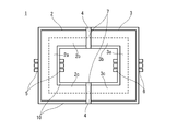
- FIG. 1 shows a configuration example of an insulation transformer (SST) according to the first embodiment.
- the insulation transformer 1 according to the first embodiment is a high frequency two-winding transformer.
- an insulation transformer 1 includes a primary side magnetic core 2, a secondary side magnetic core 3, first and second insulating members (for example, ceramics, hereinafter referred to as first and second ceramics) 4, A primary coil 5 and a secondary coil 6 are provided.
- the primary-side magnetic core 2 has a first winding portion 2a around which the primary-side coil 5 is wound, and first and second standing portions 2b and 2c that are erected at right angles from both ends of the first winding portion 2a. However, it is formed in a substantially U shape.
- the secondary side magnetic core 3 also has a second winding part 3a around which the secondary side coil 6 is wound, and third and fourth winding parts 3a standing upright from both ends of the second winding part 3a. It has standing parts 3b and 3c, and is formed in a substantially U-shape.
- the primary coil 5 is wound around the first winding portion 2a of the primary magnetic core 2, and the secondary coil 6 is wound around the second winding portion 3a of the secondary magnetic core 3.
- the first standing portion 2b of the primary side magnetic core 2 and the third standing portion 3b of the secondary side magnetic core 3, the second standing portion 2c of the primary side magnetic core 2 and the fourth standing portion 3c of the secondary side magnetic core 3 are
- the primary magnetic core 2 and the secondary magnetic core 3 are arranged so as to face each other, and are formed in a substantially square shape.
- the main magnetic flux is formed in a substantially square shape.
- the first ceramic 4 is inserted into the gap 7 between the first standing portion 2b of the primary magnetic core 2 and the third standing portion 3b of the secondary magnetic core 3. Further, the second ceramic 4 is inserted in the gap portion 7 between the second standing portion 2c of the primary side magnetic core 2 and the fourth standing portion 3c of the secondary side magnetic core 3. The first and second ceramics 4 withstand the voltage difference between the primary side and the secondary side.
- the first and second ceramics 4 are arranged so as to be orthogonal to the main magnetic flux.
- the material of the first and second ceramics 4 is, for example, silicon nitride Si3N4, aluminum nitride AlN, or the like.
- silicon nitride (Si3N4) has an insulating performance exceeding 10 kV/mm at a thickness of about 0.25 mm.
- the thin first and second ceramics 4 having high withstand voltage are inserted into the gap portion 7 of the normal two-winding transformer, and the primary side coil 5 and the secondary side coil 6 are provided, and the primary side and the secondary side coil 6 are connected.
- the main insulation is provided between the magnetic core 2 and the secondary magnetic core 3.
- the conventional SST has the gap 7 for the purpose of reducing the magnetic saturation of the magnetic core. Further, in the conventional SST, an insulating material (thickness of about several tens of millimeters) such as a thick molding material for ensuring insulation between the primary coil 5 and the secondary coil 6 is provided.
- the primary coil 5 and the secondary coil 5 are Insulation was performed between the side coils 6.
- the primary coil 5 and the secondary coil 6 can be made compact and highly insulated.
- the insulation distance on the low voltage side was the same as on the high voltage side.
- the primary side coil 5 has the minimum insulation required for the primary side circuit voltage.
- the secondary coil 6 may be the minimum degree of insulation required for the secondary circuit voltage, allowing close proximity between each coil and the magnetic core. As a result, it is possible to reduce the size and weight while satisfying the insulation performance of the insulation transformer 1. Further, since the insulation distance can be shortened, the leakage magnetic flux of each coil of the primary coil 5 and the secondary coil 6 can be reduced, and the magnetic coupling can be improved.
- FIG. 2 shows a configuration example of the insulation transformer (SST) according to the second embodiment.
- the insulation transformer 1 according to the second embodiment is one in which the conductor group of the primary side coil 5 and the conductor group of the secondary side coil 6 are covered with insulating materials 8 and 9, respectively, to provide reinforced insulation.
- the insulating materials 8 and 9 for example, a known molding material can be used.
- the second embodiment has a configuration in which insulation between the primary coil 5 and the secondary coil 6 is more necessary than in the first embodiment.
- the main insulation between the primary coil 5 and the secondary coil 6 is the first and second ceramics 4 provided in the gap portion 7 as in the first embodiment. If the insulation performance cannot be satisfied only by the main insulation of the first and second ceramics 4, in order to strengthen the insulation between the primary side coil 5 and the secondary side coil 6, each coil is molded with an insulating material 8 or 9. doing.
- the same operational effect as the first embodiment can be obtained. Further, by reinforced insulation between the primary coil 5 and the secondary coil 6, between the primary coil 5 and the secondary coil 6 even if the insulation performance cannot be satisfied only by the main insulation of the first and second ceramics 4. The insulation can be strengthened. Further, since the main insulation is provided by the first and second ceramics 4, the reinforced insulation of the primary coil 5 and the secondary coil 6 is minimal, and the SST alone can be made smaller and lighter. Becomes
- FIG. 3 shows an example of the configuration of the insulation transformer (SST) according to the third embodiment.
- the insulation transformer 1 according to the third embodiment has a minimum creeping distance for insulation between the primary coil 5 and the secondary coil 6 by minimizing the size of the insulation system. is there.
- the insulation transformer 1 shown in FIG. 3 is the same as that of the first embodiment except for the shapes of the first and second ceramics 4.
- the first ceramic 4 is provided between the end of the first upright portion 2b of the primary magnetic core 2 and the end of the third upright portion 3b of the secondary magnetic core 3.
- a second extending portion 4c extending along.
- the second ceramic 4 includes a second base 4d provided between an end of the second standing portion 2c of the primary magnetic core 2 and an end of the fourth standing portion 3c of the secondary magnetic core 3, A third extending portion 4e extending from the peripheral edge of the second base portion 4d along the side surface of the second upright portion 2c, and extending from the peripheral edge of the second base portion 4d along the side surface of the fourth upright portion 3c. And the extended fourth extending portion 4f.
- the creepage distance is outside the first to fourth extension parts 4b, 4c, 4e, 4f (opposite of the first and second base parts 4a, 4d). Side) and the creepage distance can be secured.
- the first and second ceramics 4 of the insulation transformer 1 shown in FIG. 1 have a flat plate shape.
- the first and second ceramics 4 shown in FIG. 1 project from the first to fourth standing portions 2b, 3b, 2c, 3c of the primary magnetic core 2 and the secondary magnetic core 3.
- the device becomes large and the protruding portion is easily damaged.
- the first and second ceramics 4 in the shape shown in FIG. 3, the creepage distance can be secured, and the device can be prevented from becoming large and damaged.
- FIG. 4 shows another example of the insulation transformer 1 according to the third embodiment. Similar to FIG. 3, the other example shown in FIG. 4 also secures the creepage distance with respect to the insulation between the primary side coil 5 and the secondary side coil 6 by minimizing the size increase of the insulation system. In FIG. 4, the creepage distance is secured by covering the primary side magnetic core 2 and the secondary side magnetic core 3 with a magnetic core insulating material (general molding material) 10.
- a magnetic core insulating material generally molding material
- the creeping distance between the primary side coil 5 and the secondary side coil 6 is ensured with respect to the first exemplary embodiment while minimizing the size increase of the insulation transformer 1. It is a composition.
- the creepage distance is secured by molding the shape of the first and second ceramics 4, or the primary side magnetic core 2 and the secondary side magnetic core 3 with the magnetic core insulating material 10. As a result, it is possible to further improve the insulation performance as compared with the first embodiment.
- FIG. 5 shows a configuration example of the insulation transformer (SST) according to the fourth embodiment.
- SST insulation transformer
- FIG. 2 shows a configuration example of the insulation transformer (SST) according to the fourth embodiment.
- the angle difference between the first upright portion 2b and the third upright portion 3b and the first ceramic 4 and between the second upright portion 2c and the fourth upright portion 3c and the second ceramic 4 is different. Is provided. That is, an angle is formed between the main magnetic flux and the first and second ceramics 4.
- the angle between the first standing portion 2b and the third standing portion 3b and the first ceramic 4 is ⁇ 1, and the second standing portion 2c and the fourth standing portion 3c and the second ceramic 4 are formed.
- the angle between them is ⁇ 2.
- the first and second ceramics 4 have angles ⁇ 1 and ⁇ 2 with respect to the main magnetic flux, and the cross-sectional areas of the first to fourth standing portions 2b, 2c, 3b and 3c with respect to the main magnetic flux are set. It is an increase.
- ⁇ 1 is 0°, 180°, and 360°
- ⁇ 2 0°, 90°, 180°, 270°, and 360° are not included in the third embodiment.
- the range of ⁇ 1 is 0° ⁇ 1 ⁇ 90°, 90° ⁇ 1 ⁇ 180°, 180° ⁇ 1 ⁇ 270°, 270° ⁇ 1 ⁇ 360°.
- the range of ⁇ 2 is 0° ⁇ 2 ⁇ 90°, 90° ⁇ 2 ⁇ 180°, 180° ⁇ 2 ⁇ 270°, 270° ⁇ 2 ⁇ 360°.
- ⁇ 1 and ⁇ 2 are shown as the same angle, but they do not necessarily have to be the same angle.
- the cross-sectional area of the primary side magnetic core 2 and the secondary side magnetic core 3 in contact with the first and second ceramics 4 is increased, and the magnetic resistance of the gap portion 7 is reduced and adjusted.
- the magnetic resistance of the entire main magnetic flux can be reduced.
- FIG. 6 shows a configuration example of the insulation transformer (SST) according to the fifth embodiment.
- SST insulation transformer
- a primary side common mode coil 11a is connected to one end of the primary side coil 5.
- the primary side common mode 11b is connected to the other end of the primary side coil 5.
- the primary side common mode coil 11a and the primary side common mode coil 11b are wound around the first winding portion 2a of the primary side magnetic core 2 in the same phase. That is, one of the primary side common mode coils 11 a and 1 b is wound in the same direction as the primary side coil 5, and the other is wound in the opposite direction to the primary side coil 5.
- a secondary side common mode coil 12a is connected to one end of the secondary side coil 6.
- the secondary side common mode 12b is connected to the other end of the secondary side coil 6.
- the secondary side common mode coil 12a and the secondary side common mode coil 12b are wound around the second winding portion 3a of the secondary side magnetic core 2 in the same phase. That is, one of the secondary side common mode coils 12 a and 12 b is wound in the same direction as the secondary side coil 6, and the other is wound in the opposite direction to the secondary side coil 6.
- FIG. 6 a configuration in which the primary side coil 5 and the secondary side coil 6 are arranged inside and the primary side common mode coils 11a and 11b and the secondary side common mode coils 12a and 12b are arranged outside will be described.
- the primary side common mode coils 11a and 11b are arranged inside, the primary side coil 5 is arranged at both ends thereof, the secondary side common mode coils 12a and 12b are arranged inside, and the secondary side coil is arranged at both ends thereof. 6 may be arranged.
- both of the primary side common mode coils 11a and 11b are arranged on either one side or the other side of the primary side coil 5, and either one side or the other side of the secondary side coil 6 is arranged.
- Both of the secondary side common mode coils 12a and 12b may be arranged on one side.
- the noise includes normal mode noise (differential noise) and common mode noise, but the fifth embodiment removes common mode noise due to high frequency and stray capacitance.
- the primary side common mode coils 11a and 11b and the secondary side common mode coils 12a and 12b when a common mode current flows through each coil, magnetic fluxes strengthen each other and impedance becomes relatively large, and normal mode current is When flowing, the magnetic fluxes cancel each other and the impedance becomes relatively small.
- the common mode of the high frequency component through the insulating transformer 1 (for example, passing through the first and second ceramics 4).
- the current can be reduced.
- the common mode noise caused by the primary-secondary insulation transformer 1 can be reduced without an external circuit.
- the fifth embodiment can be applied to the second to fourth embodiments.
Landscapes
- Engineering & Computer Science (AREA)
- Power Engineering (AREA)
- Coils Of Transformers For General Uses (AREA)
Abstract
一次側磁心2は、一次側コイル5が巻かれる第1巻回部2aと、第1巻回部2aの両端から立設した第1,第2立設部2b,2cと、を有し、断面略コ字状に形成される。二次側磁心3は、二次側コイル6が巻かれる第2巻回部3aと、第2巻回部3aの両端から立設した第3,第4立設部3b,3cと、を有し、断面略コ字状に形成される。一次側磁心2の第1立設部2bと二次側磁心3の第3立設部3b、および、一次側磁心2の第2立設部2cと二次側磁心3の第4立設部3cがそれぞれ互いに向かい合うように配置される。一次側磁心2の第1立設部2bと二次側磁心3の第3立設部3bの間のギャップ部7に第1絶縁部材4が挿入される。一次側磁心2の第2立設部2cと二次側磁心3の第4立設部3cの間のギャップ部7に第2絶縁部材4に挿入される。これにより、絶縁変圧器において、絶縁性能を満足しつつ、小型化,軽量化を図る。
Description
本発明は、半導体を利用した絶縁変圧器(以下、SST(ソリッドステートトランス)と称する)の絶縁および小型化に関する。
特許文献1には、ユニット化したSSTを直列接続して高電圧化した電源装置の技術が開示されている。特許文献1は、高圧の系統やモータに合わせた広範囲な電圧への柔軟な対応とSST適用よる高周波化に対して、DC/DCコンバータやインバータといった電力回路に使用されるパワーデバイスのスイッチング損失低減や冷却構造の小型化を課題としている。また、系統電圧への昇圧が必要であり、昇圧前段における大電流経路の小型・軽量化も課題としている。
特許文献1では、SST自体の小型化、軽量化については問題としていない。しかし、SSTを直列接続することによる高電圧化ではSSTの入力と出力の間の電位差が大きくなり、装置全体の高電圧化、大容量化を実現する障害となる。また、SSTの絶縁システムは、一般的に入力コイルと出力コイルの間を樹脂によって絶縁するとともに、入力コイルおよび出力コイルと鉄心の間も絶縁している。この絶縁が大型化すれば、入力と出力の磁気結合も悪くなり、漏れ磁束が増加する。
以上示したようなことから、絶縁変圧器において、絶縁性能を満足しつつ、小型化,軽量化を図ることが課題となる。
本発明は、前記従来の問題に鑑み、案出されたもので、その一態様は、一次側コイルと、前記一次側コイルが巻かれる第1巻回部と、前記第1巻回部の両端から立設した第1,第2立設部と、を有し、断面略コ字状に形成された一次側磁心と、二次側コイルと、前記二次側コイルが巻かれる第2巻回部と、前記第2巻回部の両端から立設した第3,第4立設部と、を有し、断面略コ字状に形成された二次側磁心と、を備え、前記一次側磁心の前記第1立設部と前記二次側磁心の前記第3立設部、および、前記一次側磁心の前記第2立設部と前記二次側磁心の前記第4立設部がそれぞれ互いに向かい合うように配置された絶縁変圧器であって、前記一次側磁心の前記第1立設部と前記二次側磁心の前記第3立設部の間のギャップ部に挿入された一次側と二次側の電圧差に耐える第1絶縁部材と、前記一次側磁心の前記第2立設部と前記二次側磁心の前記第4立設部の間のギャップ部に挿入された一次側と二次側の電圧差に耐える第2絶縁部材と、を備えたことを特徴とする。
また、その一態様として、前記一次側コイル、および、前記二次側コイルをそれぞれ絶縁材で覆うことを特徴とする。
また、その一態様として、前記第1絶縁部材は、前記一次側磁心の前記第1立設部の端部と前記二次側磁心の前記第3立設部の端部との間に設けられる第1基部と、前記第1基部の周縁から前記一次側磁心の前記第1立設部の側面に沿って延設された第1延設部と、前記第1基部の周縁から前記二次側磁心の前記第3立設部の側面に沿って延設された第2延設部と、を有し、前記第2絶縁部材は、前記一次側磁心の前記第2立設部の端部と前記二次側磁心の前記第4立設部の端部との間に設けられる第2基部と、前記第2基部の周縁から前記一次側磁心の前記第2立設部の側面に沿って延設された第3延設部と、前記第2基部の周縁から前記二次側磁心の前記第4立設部の側面に沿って延設された第4延設部と、を有することを特徴とする。
また、他の態様として、前記一次側磁心および前記二次側磁心を絶縁材で覆うことを特徴とする。
また、その一態様として、前記第1絶縁部材は、前記一次側磁心の前記第1立設部と前記二次側磁心の前記第3立設部に対して、0°、90°、180°、270°、360°以外の角度で設けられ、前記第2絶縁部材は、前記一次側磁心の前記第2立設部と前記二次側磁心の前記第4立設部に対して、0°、90°、180°、270°、360°以外の角度で設けられたことを特徴とする。
また、その一態様として、前記一次側コイルと接続され、前記一次側磁心の前記第1巻回部に巻かれた2つの一次側コモンモードコイルと、前記二次側コイルと接続され、前記二次側磁心の前記第2巻回部に巻かれた2つの二次側コモンモードコイルと、を備えたことを特徴とする。
また、その一態様として、前記第1絶縁部材および前記第2絶縁部材は、セラミックから成ることを特徴とする。
本発明によれば、絶縁変圧器において、絶縁性能を満足しつつ、小型化,軽量化を図ることが可能となる。
以下、本願発明における絶縁変圧器の実施形態1~5を図1~図6に基づいて詳述する。
[実施形態1]
図1に本実施形態1における絶縁変圧器(SST)の構成例を示す。図1に示すように、本実施形態1における絶縁変圧器1は高周波の2巻線変圧器である。図1に示すように、絶縁変圧器1は、一次側磁心2と、二次側磁心3と、第1,第2絶縁部材(例えばセラミック、以下第1,第2セラミックと称する)4と、一次側コイル5と、二次側コイル6と、を備える。
図1に本実施形態1における絶縁変圧器(SST)の構成例を示す。図1に示すように、本実施形態1における絶縁変圧器1は高周波の2巻線変圧器である。図1に示すように、絶縁変圧器1は、一次側磁心2と、二次側磁心3と、第1,第2絶縁部材(例えばセラミック、以下第1,第2セラミックと称する)4と、一次側コイル5と、二次側コイル6と、を備える。
一次側磁心2は、一次側コイル5が巻かれる第1巻回部2aと、第1巻回部2aの両端から直角に立設した第1,第2立設部2b,2cと、を有し、略コ字状に形成される。二次側磁心3も、一次側磁心2と同様に、二次側コイル6が巻かれる第2巻回部3aと、第2巻回部3aの両端から直角に立設した第3,第4立設部3b,3cと、を有し、略コ字状に形成される。
一次側磁心2の第1巻回部2aには一次側コイル5が巻かれ、二次側磁心3の第2巻回部3aには二次側コイル6が巻かれる。
一次側磁心2の第1立設部2bと二次側磁心3の第3立設部3b,一次側磁心2の第2立設部2cと二次側磁心3の第4立設部3cは互いに向かい合うように配置され、一次側磁心2と二次側磁心3とで略ロ字状に形成される。この一次側磁心2,二次側磁心3に沿って、主磁束が略ロ字状に形成される。
一次側磁心2の第1立設部2bと二次側磁心3の第3立設部3bの間のギャップ部7には第1セラミック4が挿入される。また、一次側磁心2の第2立設部2cと二次側磁心3の第4立設部3cの間のギャップ部7には第2セラミック4が挿入される。前記第1,第2セラミック4は一次側と二次側の電圧差に耐えるものとする。
本実施形態1において、この第1,第2セラミック4は主磁束に直交するように配置している。第1,第2セラミック4の材質は、例えば、窒化ケイ素Si3N4や窒化アルミニウムAlN等である。例えば、窒化ケイ素(Si3N4)は0.25mm程度の厚みで10kV/mmを上回る絶縁性能を有している。
本実施形態1は、通常の2巻線変圧器のギャップ部7に高耐圧の薄い第1,第2セラミック4を挿入し、一次側コイル5と二次側コイル6の間、および、一次側磁心2と二次側磁心3の間を主絶縁するものである。
従来のSSTは、磁心の磁気飽和を低減する目的でギャップ部7を設けている。また、従来のSSTは、一次側コイル5と二次側コイル6の間の絶縁を確保するための分厚いモールド材等の絶縁材(数十mm程度の厚み)を設けていた。
これに対し、本実施形態1は、ギャップ部7に非常に薄い(0.25~0.5mm程度)高耐圧の第1,第2セラミック4を挿入することにより、一次側コイル5と二次側コイル6の間の絶縁を行った。これにより、一次側コイル5と二次側コイル6を小型で高絶縁化できる。
一次側と二次側の電位差が大きい場合、従来は、低圧側も高圧側と同様の絶縁距離が必要であった。しかし、第1,第2セラミック4において、一次側コイル5と二次側コイル6の間を高絶縁化することにより、一次側コイル5は一次側の回路電圧に必要な最低限度の絶縁、二次側コイル6は二次側の回路電圧に必要な最低限度の絶縁でよく、各々のコイルと磁心の間を接近できる。その結果、絶縁変圧器1の絶縁性能を満足させつつ、小型化,軽量化させることが可能となる。また、絶縁距離を短くできるため、一次側コイル5と二次側コイル6の各コイルの漏れ磁束を低減でき、磁気結合を改善できる。
[実施形態2]
図2に本実施形態2における絶縁変圧器(SST)の構成例を示す。以下、実施形態1(図1)との相違点を説明する。図2に示すように、本実施形態2における絶縁変圧器1は、一次側コイル5の導体群と二次側コイル6の導体群を各々絶縁材8,9で覆い、強化絶縁を施したものである。絶縁材8,9は、例えば、公知のモールド材を使用することができる。
図2に本実施形態2における絶縁変圧器(SST)の構成例を示す。以下、実施形態1(図1)との相違点を説明する。図2に示すように、本実施形態2における絶縁変圧器1は、一次側コイル5の導体群と二次側コイル6の導体群を各々絶縁材8,9で覆い、強化絶縁を施したものである。絶縁材8,9は、例えば、公知のモールド材を使用することができる。
本実施形態2は、実施形態1に対して、より一次側コイル5と二次側コイル6間の絶縁が必要な場合の構成である。一次側コイル5と二次側コイル6の間の主絶縁は実施形態1と同様に、ギャップ部7に設けられた第1,第2セラミック4である。この第1,第2セラミック4の主絶縁だけでは絶縁性能を満足できない場合、一次側コイル5と二次側コイル6間の絶縁を強化するために、各々のコイルを絶縁材8,9でモールドしている。
以上示したように、本実施形態2によれば、実施形態1と同様の作用効果を奏する。また、一次側コイル5と二次側コイル6を強化絶縁することにより、第1,第2セラミック4の主絶縁だけでは絶縁性能を満足できない場合でも一次側コイル5と二次側コイル6間の絶縁を強化することができる。また、第1,第2セラミック4により、主絶縁を施しているため、一次側コイル5と二次側コイル6の強化絶縁は最低限で良く、SST単体で小型化・軽量化することが可能となる。
[実施形態3]
図3に本実施形態3における絶縁変圧器(SST)の構成の一例を示す。以下、実施形態1(図1)との相違点を説明する。図3に示すように、本実施形態3における絶縁変圧器1は、一次側コイル5と二次側コイル6間の絶縁に関して、絶縁システムの大型化を最小限にして沿面距離を確保したものである。図3に示す絶縁変圧器1は第1,第2セラミック4の形状以外は実施形態1と同様である。
図3に本実施形態3における絶縁変圧器(SST)の構成の一例を示す。以下、実施形態1(図1)との相違点を説明する。図3に示すように、本実施形態3における絶縁変圧器1は、一次側コイル5と二次側コイル6間の絶縁に関して、絶縁システムの大型化を最小限にして沿面距離を確保したものである。図3に示す絶縁変圧器1は第1,第2セラミック4の形状以外は実施形態1と同様である。
図3に示すように、第1セラミック4は、一次側磁心2の第1立設部2bの端部と二次側磁心3の第3立設部3bの端部との間に設けられる第1基部4aと、第1基部4aの周縁から第1立設部2bの側面に沿って延設された第1延設部4bと、第1基部4aの周縁から第3立設部3bの側面に沿って延設された第2延設部4cと、を有する。また、第2セラミック4は、一次側磁心2の第2立設部2cの端部と二次側磁心3の第4立設部3cの端部との間に設けられる第2基部4dと、第2基部4dの周縁から第2立設部2cの側面に沿って延設された第3延設部4eと、第2基部4dの周縁から第4立設部3cの側面に沿って延設された第4延設部4fと、を有する。
第1,第2セラミック4を上記のような形状とすることにより、沿面距離は第1~第4延設部4b,4c,4e,4fの外側(第1,第2基部4a,4dの反対側)に沿った距離となり、沿面距離が確保できる。
図1に示す絶縁変圧器1の第1,第2セラミック4は、平板状の形状をしている。図1に示す第1,第2セラミック4では、沿面距離を確保するために、一次側磁心2,二次側磁心3の第1~第4立設部2b,3b,2c,3cから突出しており、装置が大型化すると共に、突出した部分が破損しやすい。それに対し、第1,第2セラミック4を図3の形状とすることにより、沿面距離を確保できると共に、装置の大型化や破損を抑制することが可能となる。
図4に本実施形態3における絶縁変圧器1の他例を示す。図4に示す他例も図3と同様に、一次側コイル5と二次側コイル6間の絶縁に関して、絶縁システムの大型化を最小限にして沿面距離を確保したものである。図4では、一次側磁心2と二次側磁心3との周りを磁心絶縁材(一般のモールド材)10で覆うことで沿面距離を確保する。
図4に示すように、一次側磁心2と二次側磁心3を磁心絶縁材10で覆うことにより、一次側磁心2と二次側磁心3の間の沿面距離は考慮する必要がなくなる。
以上示したように、本実施形態3は、実施形態1に対して、一次側コイル5と二次側コイル6間の沿面距離の確保を絶縁変圧器1の大型化を最小限にして実施した構成である。第1,第2セラミック4の形状、または、一次側磁心2,二次側磁心3を磁心絶縁材10でモールドすることで沿面距離を確保する。これにより、実施形態1に対して、より絶縁性能を向上させることが可能となる。
なお、実施形態1に対して本実施形態3を適用した構成を説明したが、実施形態2に対して本実施形態3を適用することも可能である。
[実施形態4]
図5に本実施形態4における絶縁変圧器(SST)の構成例を示す。以下、実施形態2(図2)との相違点を説明する。本実施形態4は、第1立設部2bおよび第3立設部3bと第1セラミック4間、および、第2立設部2cおよび第4立設部3cと第2セラミック4間に角度差を設けたものである。すなわち、主磁束と第1,第2セラミック4間に角度をつける。
図5に本実施形態4における絶縁変圧器(SST)の構成例を示す。以下、実施形態2(図2)との相違点を説明する。本実施形態4は、第1立設部2bおよび第3立設部3bと第1セラミック4間、および、第2立設部2cおよび第4立設部3cと第2セラミック4間に角度差を設けたものである。すなわち、主磁束と第1,第2セラミック4間に角度をつける。
図5に示すように、第1立設部2bおよび第3立設部3bと第1セラミック4間の角度をθ1とし、第2立設部2cおよび第4立設部3cと第2セラミック4間の角度をθ2とする。本実施形態4は、第1,第2セラミック4を主磁束に対してθ1、θ2の角度を持たせ、主磁束に対する第1~第4立設部2b,2c,3b,3cの断面積を増加させたものである。
この際、θ1が90°および270°のとき、第1セラミック4と第1立設部2bおよび第3立設部3bが直角になるため、θ1=90°、270°は本実施形態3に含まれないものとする。また、θ1が0°および180°および360°のとき、第1セラミック4と第1立設部2bおよび第3立設部3bが平行になるため、θ1=0°、180°、360°は本実施形態3に含まれないものとする。θ2も同様に、θ2=0°、90°、180°、270°、360°は本実施形態3に含まないものとする。
すなわち、θ1の範囲は、0°<θ1<90°、90°<θ1<180°、180°<θ1<270°、270°<θ1<360°とする。θ2の範囲も同様に、0°<θ2<90°、90°<θ2<180°、180°<θ2<270°、270°<θ2<360°とする。なお、図5では、θ1とθ2を同じ角度として示しているが、必ずしも同じ角度とする必要はない。
以上示したように、本実施形態4によれば、第1,第2セラミック4に接する一次側磁心2,二次側磁心3の断面積を増加させ、ギャップ部7の磁気抵抗を低減、調整し、主磁束全体の磁気抵抗を低減できる。
すなわち、上記のように、第1,第2セラミック4と第1~第4立設部2b,2c,3b,3cに角度差を持たせると、第1~第4立設部2b,2c,3b,3cの断面の断面積が大きくなる。断面積が大きくなると、磁気抵抗Rm=磁路長L/(透磁率μ×断面積A)であるため、磁気抵抗Rmが減少する。
ギャップ部7の磁気抵抗が低減すると、インダクタンス=巻線の巻数N^2/(磁気抵抗Rm)に示すように、インダクタンスは磁気抵抗に反比例するため、ギャップ部7のインダクタンス(励磁インダクタンス成分)を大きくできる。また、励磁インダクタンスが大きくなれば、励磁電流が低減(励磁電流は無負荷なので、無負荷損失を低減)できる。このため、ギャップ部7付近の磁束密度が下がるため、鉄損を低減でき、鉄心の小型化を図ることが可能となる。
なお、実施形態2に対して本実施形態4を適用した構成を説明したが、実施形態1,3に対して本実施形態4を適用することも可能である。
[実施形態5]
図6に本実施形態5における絶縁変圧器(SST)の構成例を示す。以下、実施形態1(図1)との相違点を説明する。図6に示すように、本実施形態5は、実施形態1に対して一次側コモンモードコイル11a,11b、および、二次側コモンモードコイル12a,12bを付加したものである。
図6に本実施形態5における絶縁変圧器(SST)の構成例を示す。以下、実施形態1(図1)との相違点を説明する。図6に示すように、本実施形態5は、実施形態1に対して一次側コモンモードコイル11a,11b、および、二次側コモンモードコイル12a,12bを付加したものである。
一次側コイル5の一端には一次側コモンモードコイル11aが接続される。一次側コイル5の他端には一次側コモンモード11bが接続される。一次側コモンモードコイル11aと一次側コモンモードコイル11bは、同相で一次側磁心2の第1巻回部2aに巻かれる。すなわち、一次側コモンモードコイル11a,1bのうち一方は一次側コイル5と同じ向きで巻かれ、他方は一次側コイル5と逆向きで巻かれる。
二次側コイル6の一端には二次側コモンモードコイル12aが接続される。二次側コイル6の他端には二次側コモンモード12bが接続される。二次側コモンモードコイル12aと二次側コモンモードコイル12bは、同相で二次側磁心2の第2巻回部3aに巻かれる。すなわち、二次側コモンモードコイル12a,12bのうち一方は二次側コイル6と同じ向きで巻かれ、他方は二次側コイル6と逆向きで巻かれる。
なお、図6では、内側に一次側コイル5,二次側コイル6を配置し、外側に一次側コモンモードコイル11a,11b,二次側コモンモードコイル12a,12bを配置した構成について説明しているが、一次側コモンモードコイル11a,11bを内側に配置し、その両端に一次側コイル5を配置し、二次側コモンモードコイル12a,12bを内側に配置し、その両端に二次側コイル6を配置しても良い。また、一次側コイル5の一端側または他端側のうち何れか一方に、一次側コモンモードコイル11a,11bの両方を配置し、二次側コイル6の一端側または他端側のうち何れか一方に二次側コモンモードコイル12a,12bの両方を配置しても良い。
ノイズには、ノーマルモードノイズ(ディファレンシャルノイズ)とコモンモードノイズがあるが、本実施形態5は、高周波および浮遊容量に起因するコモンモードノイズを除去するものである。一次側コモンモードコイル11a,11b、および、二次側コモンモードコイル12a,12bは、各コイルにコモンモード電流が流れる場合には磁束が互いに強め合いインピーダンスが相対的に大きくなり、ノーマルモード電流が流れる場合には磁束が互いに打ち消し合いインピーダンスが相対的に小さくなるように構成されている。
一次側コモンモードコイル11a,11b,二次側コモンモードコイル12a,12bを付加することによって、絶縁変圧器1を介した(例えば、第1,第2セラミック4を通過する)高周波成分のコモンモード電流を低減することができる。これにより一次、二次間の絶縁変圧器1に起因するコモンモードノイズを外部回路なしで低減できる。
なお、実施形態1に対して実施形態5を適用した構成を説明したが、実施形態2~4に対して実施形態5を適用することも可能である。
以上、本発明において、記載された具体例に対してのみ詳細に説明したが、本発明の技術思想の範囲で多彩な変形および修正が可能であることは、当業者にとって明白なことであり、このような変形および修正が特許請求の範囲に属することは当然のことである。
Claims (7)
- 一次側コイルと、
前記一次側コイルが巻かれる第1巻回部と、前記第1巻回部の両端から立設した第1,第2立設部と、を有し、断面略コ字状に形成された一次側磁心と、
二次側コイルと、
前記二次側コイルが巻かれる第2巻回部と、前記第2巻回部の両端から立設した第3,第4立設部と、を有し、断面略コ字状に形成された二次側磁心と、
を備え、前記一次側磁心の前記第1立設部と前記二次側磁心の前記第3立設部、および、前記一次側磁心の前記第2立設部と前記二次側磁心の前記第4立設部がそれぞれ互いに向かい合うように配置された絶縁変圧器であって、
前記一次側磁心の前記第1立設部と前記二次側磁心の前記第3立設部の間のギャップ部に挿入された一次側と二次側の電圧差に耐える第1絶縁部材と、
前記一次側磁心の前記第2立設部と前記二次側磁心の前記第4立設部の間のギャップ部に挿入された一次側と二次側の電圧差に耐える第2絶縁部材と、を備えた絶縁変圧器。 - 前記一次側コイル、および、前記二次側コイルをそれぞれ絶縁材で覆う請求項1記載の絶縁変圧器。
- 前記第1絶縁部材は、
前記一次側磁心の前記第1立設部の端部と前記二次側磁心の前記第3立設部の端部との間に設けられる第1基部と、
前記第1基部の周縁から前記一次側磁心の前記第1立設部の側面に沿って延設された第1延設部と、
前記第1基部の周縁から前記二次側磁心の前記第3立設部の側面に沿って延設された第2延設部と、を有し、
前記第2絶縁部材は、
前記一次側磁心の前記第2立設部の端部と前記二次側磁心の前記第4立設部の端部との間に設けられる第2基部と、
前記第2基部の周縁から前記一次側磁心の前記第2立設部の側面に沿って延設された第3延設部と、
前記第2基部の周縁から前記二次側磁心の前記第4立設部の側面に沿って延設された第4延設部と、を有する請求項1または2記載の絶縁変圧器。 - 前記一次側磁心および前記二次側磁心を絶縁材で覆う請求項1または2に記載の絶縁変圧器。
- 前記第1絶縁部材は、前記一次側磁心の前記第1立設部と前記二次側磁心の前記第3立設部に対して、0°、90°、180°、270°、360°以外の角度で設けられ、
前記第2絶縁部材は、前記一次側磁心の前記第2立設部と前記二次側磁心の前記第4立設部に対して、0°、90°、180°、270°、360°以外の角度で設けられた請求項1~4のうち何れかに記載の絶縁変圧器。 - 前記一次側コイルと接続され、前記一次側磁心の前記第1巻回部に巻かれた2つの一次側コモンモードコイルと、
前記二次側コイルと接続され、前記二次側磁心の前記第2巻回部に巻かれた2つの二次側コモンモードコイルと、を備えた請求項1~5のうち何れかに記載の絶縁変圧器。 - 前記第1絶縁部材および前記第2絶縁部材は、セラミックから成る請求項1~6のうち何れかに記載の絶縁変圧器。
Applications Claiming Priority (2)
| Application Number | Priority Date | Filing Date | Title |
|---|---|---|---|
| JP2019027025 | 2019-02-19 | ||
| JP2019-027025 | 2019-02-19 |
Publications (1)
| Publication Number | Publication Date |
|---|---|
| WO2020170499A1 true WO2020170499A1 (ja) | 2020-08-27 |
Family
ID=72143453
Family Applications (1)
| Application Number | Title | Priority Date | Filing Date |
|---|---|---|---|
| PCT/JP2019/040384 Ceased WO2020170499A1 (ja) | 2019-02-19 | 2019-10-15 | 絶縁変圧器 |
Country Status (1)
| Country | Link |
|---|---|
| WO (1) | WO2020170499A1 (ja) |
Cited By (1)
| Publication number | Priority date | Publication date | Assignee | Title |
|---|---|---|---|---|
| CN114551377A (zh) * | 2022-04-24 | 2022-05-27 | 杭州飞仕得科技有限公司 | 一种igbt驱动封装结构及制作方法 |
Citations (7)
| Publication number | Priority date | Publication date | Assignee | Title |
|---|---|---|---|---|
| JPS55140211A (en) * | 1979-04-10 | 1980-11-01 | Philips Nv | Cctype core transformer |
| JPS57132308A (en) * | 1981-02-09 | 1982-08-16 | Honda Motor Co Ltd | Iron core for closed magnetic path type ignition coil |
| JPS60260119A (ja) * | 1984-06-07 | 1985-12-23 | Nippon Telegr & Teleph Corp <Ntt> | 雑音阻止複合トランス |
| JPH0327507A (ja) * | 1989-06-23 | 1991-02-05 | Mitsubishi Electric Corp | リアクトル付トランス |
| JPH04105517U (ja) * | 1991-02-20 | 1992-09-10 | 松下電器産業株式会社 | トランス |
| JPH06132146A (ja) * | 1992-10-15 | 1994-05-13 | Matsushita Electric Ind Co Ltd | トランスおよびそれを用いた電子機器 |
| JPH08288159A (ja) * | 1995-04-12 | 1996-11-01 | Kodera Denshi Seisakusho:Kk | 漏れ磁束トランス |
-
2019
- 2019-10-15 WO PCT/JP2019/040384 patent/WO2020170499A1/ja not_active Ceased
Patent Citations (7)
| Publication number | Priority date | Publication date | Assignee | Title |
|---|---|---|---|---|
| JPS55140211A (en) * | 1979-04-10 | 1980-11-01 | Philips Nv | Cctype core transformer |
| JPS57132308A (en) * | 1981-02-09 | 1982-08-16 | Honda Motor Co Ltd | Iron core for closed magnetic path type ignition coil |
| JPS60260119A (ja) * | 1984-06-07 | 1985-12-23 | Nippon Telegr & Teleph Corp <Ntt> | 雑音阻止複合トランス |
| JPH0327507A (ja) * | 1989-06-23 | 1991-02-05 | Mitsubishi Electric Corp | リアクトル付トランス |
| JPH04105517U (ja) * | 1991-02-20 | 1992-09-10 | 松下電器産業株式会社 | トランス |
| JPH06132146A (ja) * | 1992-10-15 | 1994-05-13 | Matsushita Electric Ind Co Ltd | トランスおよびそれを用いた電子機器 |
| JPH08288159A (ja) * | 1995-04-12 | 1996-11-01 | Kodera Denshi Seisakusho:Kk | 漏れ磁束トランス |
Cited By (1)
| Publication number | Priority date | Publication date | Assignee | Title |
|---|---|---|---|---|
| CN114551377A (zh) * | 2022-04-24 | 2022-05-27 | 杭州飞仕得科技有限公司 | 一种igbt驱动封装结构及制作方法 |
Similar Documents
| Publication | Publication Date | Title |
|---|---|---|
| US20080224809A1 (en) | Magnetic integration structure | |
| US11705260B2 (en) | Magnetic device including winding and insulators, and power conversion device using the same | |
| EP1213833A1 (en) | Choke coil | |
| KR20180129470A (ko) | 변압기 및 이를 가지는 llc 공진형 컨버터 | |
| US11735357B2 (en) | Transformer with improved insulation structure | |
| CN210575456U (zh) | 一种提高功率密度的集成磁性元件 | |
| CN104025213A (zh) | 电感性组件和使用 | |
| CN104465035A (zh) | 电抗器和电力转换器 | |
| WO2019013131A1 (ja) | プレーナ型トランス及びdcdcコンバータ | |
| KR20140041867A (ko) | 리액터 및 전기 기기 | |
| US20230360850A1 (en) | Converter component and converter | |
| JP7328815B2 (ja) | 磁気結合型インダクタ | |
| WO2020170499A1 (ja) | 絶縁変圧器 | |
| WO2018070198A1 (ja) | 変圧器およびそれを備えた電力変換器 | |
| JP2025160377A (ja) | リーケージトランス | |
| JPH11345715A (ja) | 小形電気巻線部品 | |
| KR101932232B1 (ko) | 전원공급장치의 트랜스포머용 분리형 보빈 구조 | |
| JP7269699B2 (ja) | コア、トランス | |
| JP7420092B2 (ja) | 絶縁トランス | |
| JP3402573B2 (ja) | トランス及び電源 | |
| KR101456525B1 (ko) | 양방향 고주파 변압기 | |
| JP4300494B2 (ja) | 高周波パワートランスおよびこれを用いた電力変換装置 | |
| JP2000299232A (ja) | 共振型電源用トランス | |
| EP3373312B1 (en) | Transformer and dc-dc converter | |
| TWI846359B (zh) | 用於交錯式諧振電路架構之磁性元件集成結構 |
Legal Events
| Date | Code | Title | Description |
|---|---|---|---|
| 121 | Ep: the epo has been informed by wipo that ep was designated in this application |
Ref document number: 19916406 Country of ref document: EP Kind code of ref document: A1 |
|
| NENP | Non-entry into the national phase |
Ref country code: DE |
|
| 122 | Ep: pct application non-entry in european phase |
Ref document number: 19916406 Country of ref document: EP Kind code of ref document: A1 |