WO2020162227A1 - レーザー走査装置および測距装置 - Google Patents
レーザー走査装置および測距装置 Download PDFInfo
- Publication number
- WO2020162227A1 WO2020162227A1 PCT/JP2020/002527 JP2020002527W WO2020162227A1 WO 2020162227 A1 WO2020162227 A1 WO 2020162227A1 JP 2020002527 W JP2020002527 W JP 2020002527W WO 2020162227 A1 WO2020162227 A1 WO 2020162227A1
- Authority
- WO
- WIPO (PCT)
- Prior art keywords
- liquid crystal
- transparent
- scanning device
- laser scanning
- pair
- Prior art date
- Legal status (The legal status is an assumption and is not a legal conclusion. Google has not performed a legal analysis and makes no representation as to the accuracy of the status listed.)
- Ceased
Links
Images








Classifications
-
- G—PHYSICS
- G01—MEASURING; TESTING
- G01C—MEASURING DISTANCES, LEVELS OR BEARINGS; SURVEYING; NAVIGATION; GYROSCOPIC INSTRUMENTS; PHOTOGRAMMETRY OR VIDEOGRAMMETRY
- G01C3/00—Measuring distances in line of sight; Optical rangefinders
- G01C3/02—Details
- G01C3/06—Use of electric means to obtain final indication
-
- G—PHYSICS
- G01—MEASURING; TESTING
- G01S—RADIO DIRECTION-FINDING; RADIO NAVIGATION; DETERMINING DISTANCE OR VELOCITY BY USE OF RADIO WAVES; LOCATING OR PRESENCE-DETECTING BY USE OF THE REFLECTION OR RERADIATION OF RADIO WAVES; ANALOGOUS ARRANGEMENTS USING OTHER WAVES
- G01S7/00—Details of systems according to groups G01S13/00, G01S15/00, G01S17/00
- G01S7/48—Details of systems according to groups G01S13/00, G01S15/00, G01S17/00 of systems according to group G01S17/00
- G01S7/481—Constructional features, e.g. arrangements of optical elements
-
- G—PHYSICS
- G02—OPTICS
- G02F—OPTICAL DEVICES OR ARRANGEMENTS FOR THE CONTROL OF LIGHT BY MODIFICATION OF THE OPTICAL PROPERTIES OF THE MEDIA OF THE ELEMENTS INVOLVED THEREIN; NON-LINEAR OPTICS; FREQUENCY-CHANGING OF LIGHT; OPTICAL LOGIC ELEMENTS; OPTICAL ANALOGUE/DIGITAL CONVERTERS
- G02F1/00—Devices or arrangements for the control of the intensity, colour, phase, polarisation or direction of light arriving from an independent light source, e.g. switching, gating or modulating; Non-linear optics
- G02F1/01—Devices or arrangements for the control of the intensity, colour, phase, polarisation or direction of light arriving from an independent light source, e.g. switching, gating or modulating; Non-linear optics for the control of the intensity, phase, polarisation or colour
- G02F1/13—Devices or arrangements for the control of the intensity, colour, phase, polarisation or direction of light arriving from an independent light source, e.g. switching, gating or modulating; Non-linear optics for the control of the intensity, phase, polarisation or colour based on liquid crystals, e.g. single liquid crystal display cells
-
- G—PHYSICS
- G02—OPTICS
- G02F—OPTICAL DEVICES OR ARRANGEMENTS FOR THE CONTROL OF LIGHT BY MODIFICATION OF THE OPTICAL PROPERTIES OF THE MEDIA OF THE ELEMENTS INVOLVED THEREIN; NON-LINEAR OPTICS; FREQUENCY-CHANGING OF LIGHT; OPTICAL LOGIC ELEMENTS; OPTICAL ANALOGUE/DIGITAL CONVERTERS
- G02F1/00—Devices or arrangements for the control of the intensity, colour, phase, polarisation or direction of light arriving from an independent light source, e.g. switching, gating or modulating; Non-linear optics
- G02F1/01—Devices or arrangements for the control of the intensity, colour, phase, polarisation or direction of light arriving from an independent light source, e.g. switching, gating or modulating; Non-linear optics for the control of the intensity, phase, polarisation or colour
- G02F1/13—Devices or arrangements for the control of the intensity, colour, phase, polarisation or direction of light arriving from an independent light source, e.g. switching, gating or modulating; Non-linear optics for the control of the intensity, phase, polarisation or colour based on liquid crystals, e.g. single liquid crystal display cells
- G02F1/133—Constructional arrangements; Operation of liquid crystal cells; Circuit arrangements
- G02F1/1333—Constructional arrangements; Manufacturing methods
- G02F1/1337—Surface-induced orientation of the liquid crystal molecules, e.g. by alignment layers
-
- G—PHYSICS
- G02—OPTICS
- G02F—OPTICAL DEVICES OR ARRANGEMENTS FOR THE CONTROL OF LIGHT BY MODIFICATION OF THE OPTICAL PROPERTIES OF THE MEDIA OF THE ELEMENTS INVOLVED THEREIN; NON-LINEAR OPTICS; FREQUENCY-CHANGING OF LIGHT; OPTICAL LOGIC ELEMENTS; OPTICAL ANALOGUE/DIGITAL CONVERTERS
- G02F1/00—Devices or arrangements for the control of the intensity, colour, phase, polarisation or direction of light arriving from an independent light source, e.g. switching, gating or modulating; Non-linear optics
- G02F1/29—Devices or arrangements for the control of the intensity, colour, phase, polarisation or direction of light arriving from an independent light source, e.g. switching, gating or modulating; Non-linear optics for the control of the position or the direction of light beams, i.e. deflection
Definitions
- the present invention relates to a laser scanning device and a distance measuring device.
- Patent Document 1 Japanese Patent Laid-Open No. 2017-15404 (Patent Document 1) and International Publication No. 2017/154910 (Patent Document 2) have been proposed.
- Japanese Unexamined Patent Application Publication No. 2017-15404 discloses, as a distance measuring device, an optical scanning device that irradiates a rotating polygon mirror with laser light and scans the laser light.
- a laser scanning device includes substrates (21) and (22) disposed opposite to each other, a liquid crystal layer (23) sandwiched between the substrates (21) and (22), and a substrate. (21), a plurality of unit electrodes (25) each having a plurality of cell electrodes arranged along the first direction, a common electrode (26) provided on the substrate (22), and a plurality of cells.
- the laser scanning device tends to increase in size due to the increase in size of the polygon mirror.
- miniaturization of the laser scanning device is desired.
- the polygon mirror is rotated by the motor, there is a problem in durability of mechanical parts of the polygon mirror and the motor, and there is also a problem that the scanning speed of the laser is limited by the rotation speed of the motor. Therefore, there is a demand for a mechanicalless laser scanning device having no mechanical section.
- International Publication No. 2017/154910 is a method of bending light by applying different voltages to a plurality of unit electrodes (25). Since it is necessary to control the voltage for each of the plurality of unit electrodes (25), it is considered that the voltage control becomes complicated. In addition, since voltage is applied to the plurality of unit electrodes (25), it is considered that power consumption will increase.
- An object of the present invention is to provide a laser scanning device capable of reducing power consumption.
- the laser scanning device includes a first transparent substrate, a second transparent substrate, a liquid crystal layer provided between the first transparent substrate and the second transparent substrate, and the first transparent substrate.
- a pair of transparent electrodes provided on one of the substrate and the second transparent substrate, and a transparent electrode provided and arranged on the other of the first transparent substrate and the second transparent substrate.
- Laser light is scanned by controlling the voltage applied between the pair of transparent electrodes and the transparent electrode.
- the laser scanning device also includes a first liquid crystal element and a second liquid crystal element.
- the first liquid crystal element has a first transparent electrode, a pair of second transparent electrodes, and a first liquid crystal layer.
- the second liquid crystal element has a third transparent electrode, a pair of fourth transparent electrodes, and a second liquid crystal layer.
- the pair of second transparent electrodes are arranged along a first direction, and the pair of fourth transparent electrodes are arranged along a second direction different from the first direction.
- the laser beam is scanned in the second direction by controlling the voltage applied between the first transparent electrode and the pair of second transparent electrodes.
- the laser beam is scanned in the first direction by controlling the voltage applied between the third transparent electrode and the pair of fourth transparent electrodes.
- FIG. 2 is a plan view for explaining a schematic configuration of the laser scanning device of FIG. 1. It is a figure explaining the combination of the liquid crystal element and the light emitting element of FIG. It is a perspective view which shows the liquid crystal element of FIG. It is a figure explaining the 1st scanning example of the laser scanning device of FIG. It is a figure explaining the 2nd scanning example of the laser scanning device of FIG. It is sectional drawing which shows the structure of a laser scanning device when a positive type liquid crystal material is used for a liquid crystal layer.
- FIG. 9 is a perspective view showing the liquid crystal element of FIG. 7. It is a figure explaining the 1st scanning example of the laser scanning device of FIG.
- FIG. 8 is a perspective view showing a configuration example of a laser scanning device using two liquid crystal elements shown in FIG. 7. It is a figure explaining an example of the scanning method of the laser scanning device shown in FIG. It is a figure which shows the structural example 1 of the distance measuring device which concerns on embodiment. It is a figure which shows the structural example 2 of the distance measuring device which concerns on embodiment. It is a figure which shows the structural example 3 of the distance measuring device which concerns on embodiment.
- FIG. 1 is a sectional view showing a configuration example of a laser scanning device according to an embodiment.
- FIG. 2 is a plan view for explaining the schematic configuration of the laser scanning device of FIG.
- the laser scanning device 1 shown in FIG. 1 is, for example, a laser scanning device included in a distance measuring device used for vehicle detection of an automobile.
- the distance measuring device is called LIDAR (Light Detection And Ranging, Laser Imaging Detection And Ranging), and as will be described later, a laser element for irradiating a laser beam and a laser scanning device 1 for scanning the laser beam, And a detection device.
- LIDAR Light Detection And Ranging, Laser Imaging Detection And Ranging
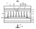
- the laser scanning device 1 includes a liquid crystal element 2.
- the liquid crystal element 2 is provided on the first transparent substrate 10, the second transparent substrate 12, the horizontal alignment film 14 provided on the upper surface of the first transparent substrate 10, and the lower surface of the second transparent substrate 12.
- Vertical alignment film 16 a sealing material 18 provided between the horizontal alignment film 14 and the vertical alignment film 16, and a liquid crystal layer provided between the horizontal alignment film 14, the vertical alignment film 16 and the sealing material 18. 20 is included.
- the liquid crystal layer 20 is made of a positive type liquid crystal material.
- the height of the sealing material 18 is, for example, about 5 to 10 ⁇ m.
- the orientation is a hybrid orientation.
- the first transparent substrate 10 includes a glass substrate 101 and two comb-teeth-shaped transparent electrodes 102 and 103 provided on the upper surface of the glass substrate 101.
- the pair of comb-teeth-shaped transparent electrodes 102 and 103 can be made of, for example, ITO (Indium Tin Oxide).
- the second transparent substrate 12 includes a glass substrate 121, a transparent electrode 122 provided on the lower surface of the glass substrate 121, and a protrusion 123 selectively provided on the lower surface of the transparent electrode 122.
- the transparent electrode 122 can be made of, for example, ITO (Indium Tin Oxide).
- the transparent electrode 122 is provided on the entire lower surface (entire surface) of the glass substrate 121.
- the projecting portion 123 can be configured by selectively providing an insulating film on the surface of the transparent electrode 122 corresponding to a substantially middle position of the sealing material 18 provided on both sides in a cross-sectional view.
- the protrusion 123 can be formed of, for example, an organic insulating film formed of an organic insulating material.
- the protrusion 123 may be an inorganic insulating film made of an inorganic insulating material.
- the protrusion 123 has a triangular shape in a cross-sectional view, and the base of the triangular shape is provided so as to contact the surface of the transparent electrode 122.
- the apexes of the triangular shape are arranged so as to face the liquid crystal layer 20 side.
- the length of the base of the triangular shape is, for example, about 1 ⁇ m, and the height of the triangular shape is, for example, about 1 ⁇ m.
- the shape of the protrusion 123 may be trapezoidal. When the protrusion 123 has a trapezoidal shape, the trapezoidal lower bottom (longer one) is provided in contact with the surface of the transparent electrode 122, and the trapezoidal upper bottom (shorter one) is the liquid crystal. It is arranged to face the layer 20.
- the vertical alignment film 16 is provided on the transparent electrode 122 on which the protrusion 123 is formed.
- the protrusions 16a of the vertical alignment film 16 are formed on the protrusions 123 of the transparent electrode 122, and thereby the alignment of the liquid crystal layer 20 is controlled.
- the liquid crystal element 2 has a rectangular shape in plan view.
- the liquid crystal element 2 has a substantially square shape.
- the length in the X direction and the length in the Y direction of the liquid crystal element 2 is, for example, about 26 ⁇ m.
- the liquid crystal layer 20 is provided in a region inside the square dotted line 3 in a plan view.
- the sealing material 18 is provided outside the square dotted line 3 in a plan view, in a frame region provided so as to surround the periphery of the square dotted line 3.
- the length LL of each of the transparent electrodes 102 and 103 in the X direction is, for example, about 2 ⁇ m.
- the distance LS between the transparent electrodes 102 and 103 is, for example, about 18 ⁇ m to 20 ⁇ m.
- the length of each of the transparent electrodes 102 and 103 in the Y direction is, for example, about 24 ⁇ m.
- the protrusion 123 formed on the second transparent substrate 12 is provided at a position approximately in the middle of the interval LS between the transparent electrodes 102 and 103, and the length L123 of the protrusion 123 in the X direction is 1 ⁇ m in one example. It is a degree.
- the length of the protrusion 123 in the Y direction is, for example, about 24 ⁇ m.
- FIG. 3 is a diagram for explaining a combination of the liquid crystal element and the light emitting element of FIG.
- FIG. 4 is a perspective view showing the liquid crystal element of FIG.
- the light emitting element 40 is an element that emits a laser beam 42 such as a laser diode element. As shown in FIG. 3, the light emitting element 40 is arranged so that the laser light 42 is transmitted between the transparent electrodes 102 and 103.
- the polarization axis of the polarizing plate 30 provided in the liquid crystal element 2 is at an angle other than 90° with respect to the alignment direction. For example, it is set to 45°.
- the light emitting element 40 is a polarization type laser diode element, it is not necessary to provide the polarizing plate 30 on the liquid crystal element 2.
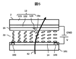
- FIG. 5 is a diagram illustrating a first scanning example of the laser scanning device according to the embodiment.
- FIG. 6 is a diagram illustrating a second scanning example of the laser scanning device according to the embodiment.
- the liquid crystal of the liquid crystal layer 20 is oriented so as to gradually incline in the horizontal direction from the state of FIG. 1 or FIG. 3 from the left side to the right side.
- the liquid crystal of the liquid crystal layer 20 located on the right side of the protrusion 123 or the protrusion 16a is gradually aligned in the horizontal direction as the distance from the protrusion 123 or the protrusion 16a increases.
- the laser light 42 can be scanned so as to bend to the right as shown in FIG.
- a voltage is applied between the transparent electrode 122 and the transparent electrode 102 so that the positive electrode voltage V is applied to the transparent electrode 102 and the ground potential GND is applied to the transparent electrode 122.
- the liquid crystal of the liquid crystal layer 20 is oriented so as to gradually incline in the horizontal direction from the state of FIG. 1 or FIG. 3 from the right side to the left side.
- the liquid crystal of the liquid crystal layer 20 positioned on the left side of the protrusion 123 or the protrusion 16a is gradually aligned in the horizontal direction as the distance from the protrusion 123 or the protrusion 16a increases.
- the laser light 42 can be scanned so as to bend to the left as shown in FIG.
- the laser beam 42 can be scanned left and right.
- the maximum value of the positive potential voltage V applied to the transparent electrodes 102 and 103 is, for example, about 20V.
- the scanning angle of the laser beam 42 changes depending on the liquid crystal layer 20 and the thickness of the liquid crystal layer 20, but in one example, it is about 60 degrees on the left side and about 60 degrees on the right side, and is about 120 degrees as a whole. be able to.
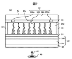
- FIG. 7 is a sectional view showing the configuration of a laser scanning device when a positive type liquid crystal material is used for the liquid crystal layer.
- FIG. 8 is a perspective view showing the liquid crystal element of FIG. 7.
- the liquid crystal element 2p of the laser scanning device 1p shown in FIG. 7 is different from the liquid crystal element 2 of the laser scanning device 1 shown in FIG. 3 in that the liquid crystal layer 20p is made of a positive type liquid crystal material and the first transparent substrate. 10 includes the transparent electrode 104 provided on the entire area (entire surface) of the upper surface of the glass substrate 101, and the second transparent substrate 12 does not include the transparent electrode 122 and is selectively provided on the lower surface of the glass substrate 121. And a point including the protruding portion 123 and the transparent electrodes 102p and 103p.
- the projecting portion 123 is selectively disposed on the lower surface of the glass substrate 121 so as to be located approximately in the middle of the transparent electrode 102p and the transparent electrode 103p in a cross-sectional view.
- the other structure is the same as that of FIG.
- a polarizing plate 30 is provided on the lower surface of the glass substrate 101.
- the light emitting element 40 is an element that emits a laser beam 42 such as a laser diode element. As shown in FIG. 7, the light emitting element 40 is arranged so that the laser beam 42 is applied to the formation region of the protrusion 123 or the protrusion 16a.
- the polarization axis of the polarizing plate 30 provided in the liquid crystal element 2p is at an angle other than 90° with respect to the alignment direction. For example, it is set to 45°.
- the light emitting element 40 is a polarization type laser diode element, it is not necessary to provide the polarizing plate 30 on the liquid crystal element 2.
- FIG. 9 is a diagram illustrating a first scanning example of the laser scanning device in FIG. 7.
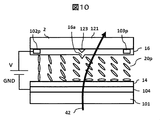
- FIG. 10 is a diagram illustrating a second scanning example of the laser scanning device in FIG. 7.
- the liquid crystal of the liquid crystal layer 20p is oriented so as to gradually invert in the vertical direction from the state of FIG. 7 toward the right side to the left side.
- the liquid crystal of the liquid crystal layer 20 located on the right side of the protrusion 123 or the protrusion 16a gradually orients in the vertical direction as the distance from the protrusion 123 or the protrusion 16a increases.
- the laser beam 42 can be scanned so as to bend to the left as shown in FIG.
- the liquid crystal of the liquid crystal layer 20p is oriented so as to gradually invert in the vertical direction from the state of FIG. 7 to the left side.
- the liquid crystal of the liquid crystal layer 20p located on the left side of the protrusion 123 or the protrusion 16a is gradually aligned in the vertical direction as the distance from the protrusion 123 or the protrusion 16a increases.
- the laser light 42 can be scanned so as to bend to the right as shown in FIG.
- the laser beam 42 can be scanned left and right.
- the maximum value of the positive potential voltage V applied to the transparent electrodes 102p and 103p is, for example, about 20V.
- the scanning angle of the laser beam 42 changes depending on the liquid crystal layer 20 and the thickness of the liquid crystal layer 20, but in one example, it is about 60 degrees on the left side and about 60 degrees on the right side, and is about 120 degrees as a whole. be able to.
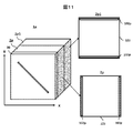
- FIG. 11 is a perspective view showing a configuration example of a laser scanning device using two liquid crystal elements 2p shown in FIG.
- the laser scanning device 1a includes a laser scanning device 1p including a liquid crystal element (first liquid crystal element) 2p and a polarizing plate 30 shown in FIG. 7, and further, a liquid crystal element 2p shown in FIG. It is combined as an element (second liquid crystal element) 2p1.
- the glass substrate 101 of the liquid crystal element 2p and the glass substrate 121 of the liquid crystal element 2p1 are preferably attached to each other by using an optical adhesive material such as a resin having a low refractive index.
- the refractive index of the optical adhesive is preferably the refractive index of the glass substrates 101 and 121.
- the liquid crystal element 2p includes a transparent electrode (first transparent electrode) 104 provided on the glass substrate 101 and a pair of transparent electrodes (second transparent electrode) provided on the glass substrate 121 of the liquid crystal element 2p as shown in FIG. Electrodes) 102p and 103p.
- the pair of transparent electrodes (second transparent electrodes) 102p and 103p are provided in a direction along the Y direction (first direction).
- the liquid crystal element 2p includes a transparent electrode (third transparent electrode) 104 provided on the glass substrate 101 and a pair of transparent electrodes (fourth transparent electrode) provided on the glass substrate 121 of the liquid crystal element 2p1 as shown in FIG. Transparent electrodes) 102p and 103p.
- the pair of transparent electrodes (fourth transparent electrodes) 102p and 103p are provided in a direction along the X direction (second direction) different from the Y direction.
- the liquid crystal element 2p can scan the laser light in the X direction by controlling the voltage applied between the transparent electrode 104 and the pair of transparent electrodes 102p and 103p.
- the liquid crystal element 2p1 can scan the laser light in the Y direction by controlling the voltage applied between the transparent electrode 104 and the pair of transparent electrodes 102p and 103p. Therefore, the laser scanning device 1a can scan the laser light in the X direction and the Y direction. That is, in the laser scanning device 1a, the scannable range of the laser light is expanded in the X direction and the Y direction.
- the order of laminating the liquid crystal element 2p and the liquid crystal element 2p1 may be exchanged. Further, the positions of the transparent electrodes 102p and 103p provided on the glass substrate 121 of the liquid crystal element 2p may be exchanged. Further, the positions of the transparent electrodes 102p and 103p provided on the glass substrate 121 of the liquid crystal element 2p1 may be exchanged.
- the liquid crystal element 2p and the liquid crystal element 2p1 can also be configured by using two liquid crystal elements 2 shown in FIG.
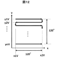
- FIG. 12 is a diagram for explaining an example of a scanning method of the laser scanning device 1a shown in FIG.
- a positive potential voltage y1V is applied to the transparent electrode 102p provided on the glass substrate 121 of the liquid crystal element 2p1.
- the positive potential applied to the transparent electrode 102p provided on the glass substrate 121 of the liquid crystal element 2p is gradually changed from x1V to 0V.
- the positive potential applied to the transparent electrode 103p provided on the glass substrate 121 of the liquid crystal element 2p is gradually changed from 0V to x2V.
- the voltage applied to the transparent electrode 102p provided on the glass substrate 121 of the liquid crystal element 2p1 is changed from y1V to y2V.
- the positive potential applied to the transparent electrode 103p provided on the glass substrate 121 of the liquid crystal element 2p is gradually changed from x2V to 0V.
- the positive potential applied to the transparent electrode 102p provided on the glass substrate 121 of the liquid crystal element 2p is gradually changed from 0V to x1V.
- the laser light is scanned in the Y direction and the X direction. it can. If the potentials applied to the transparent electrodes 102p and 103p provided on the glass substrate 121 of the liquid crystal elements 2p and 2p1 are controlled at high speed, the scanning speed of the laser light in the Y direction and the X direction can be increased.
- the scanning speed of the laser light in the Y and X directions can be changed relatively freely, it is possible to increase the detection frequency (dense) or decrease the detection frequency (coarse).
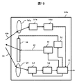
- FIG. 15 is a diagram showing a configuration example 1 of the distance measuring device according to the embodiment.
- the distance measuring device 50 includes a laser scanning device 1a, a light emitting element 40, a distance measuring calculation device 51, a voltage applying circuit 52, a half mirror 53, a light receiving lens 54, a light receiving element 57, and a signal processing device 59. ,including.
- the distance measurement calculation device 51 has a storage device that stores the scanning angle (bending angle) of the laser light 42 for each voltage applied to the laser scanning device 1a. Further, the distance measuring calculation device 51 controls the light emission of the light emitting element 40.
- the voltage application circuit 52 is controlled by the distance measurement calculation device 51, and applies the voltage instructed by the distance measurement calculation device 51 to the laser scanning device 1a.
- the laser light 42 emitted from the light emitting element 40 is input to the laser scanning device 1a via the half mirror 53.
- the laser beam 42 input to the laser scanning device 1a is scanned by the laser scanning device 1a and is applied to a detection target such as a vehicle in front.
- the reflected light 44 returning from the object to be detected is input to the laser scanning device 1a, is bent, is reflected by the half mirror 53, is condensed by the light receiving lens 54, and is input to the light receiving element 57. ..
- the signal processing device 59 performs signal processing on the information of the reflected light received by the light receiving element 57, and outputs it as data to the distance measurement calculation device 51.
- the distance measurement calculation device 51 calculates and outputs the distance and the direction or azimuth to the detection target based on the data output from the signal processing device 59.
- the distance measuring device 50 does not include a mechanical part such as a polygon mirror or a motor, and thus can be downsized. Further, since the distance measuring device 50 does not have a mechanical part, it is possible to improve durability.
- FIG. 14 is a diagram showing a configuration example 2 of the distance measuring device according to the embodiment.
- the distance measuring device 50a of FIG. 14 differs from the distance measuring device 50 of FIG. 13 in that the distance measuring device 50a does not use the half mirror 53 and that the light receiving lens 54 directly receives the reflected light 44.
- the angle of the reflected light 44 that can be collected is determined by the arrangement angle of the light receiving lens 54. Since the half mirror 53 is not used, the light amount of the laser light 42 emitted from the light emitting element 40 can be effectively utilized.
- a plurality of light receiving lenses 54 may be provided.
- the other structure is the same as that of the distance measuring device 50 in FIG. 14, and thus the description thereof is omitted.
- FIG. 15 is a diagram showing a configuration example 3 of the distance measuring device according to the embodiment.
- the distance measuring device 50b of FIG. 15 differs from the distance measuring device 50a of FIG. 14 in that a light receiving lens 54a, a light receiving element 57a, and a signal processing device 59a are provided. That is, by detecting the reflected light 44, 44a by the light receiving lenses 54, 54a and the light receiving elements 57, 57a, the angle of the reflected light that can be condensed can be expanded.
- the other configuration is the same as that of the distance measuring device 50a in FIG.
- the laser scanning device 1 (1p) includes a liquid crystal layer 20 provided between a first transparent substrate 10 and a second transparent substrate 12, a first transparent substrate 10 and a second transparent substrate 12.
- Laser light can be scanned by controlling the voltage applied between the pair of transparent electrodes 102, 103 (102p, 103p) and the transparent electrode 122 (104).
- the protrusion 123 is provided in the region of the second transparent substrate 12 located between the pair of transparent electrodes 102, 103 (102p, 103p), the alignment of the liquid crystal layer 20 can be controlled.
- the liquid crystal layer 20 is provided.
- the initial orientation of can be controlled.
- the laser scanning device 1a includes a liquid crystal element (first liquid crystal element) 2p and a liquid crystal element (second liquid crystal element) 2p1.
- the pair of first transparent electrodes 102p and 103p of the liquid crystal element 2p are provided in the direction along the Y direction (first direction).
- the pair of second transparent electrodes 102p and 103p provided on the glass substrate 121 of the liquid crystal element 2p1 are provided in a direction along the X direction (second direction) different from the Y direction. Accordingly, the laser scanning device 1a can scan the laser light in the X direction and the Y direction.
- the distance measuring device (50, 50a, 50b) including the laser scanning device 1a does not include a mechanical part such as a polygon mirror or a motor, the distance measuring device can be downsized. Further, since the distance measuring device does not have a mechanical part, the durability of the distance measuring device can be improved.
- Various inventions can be formed by appropriately combining a plurality of constituent elements disclosed in the above embodiments. For example, some components may be deleted from all the components shown in the embodiment. Furthermore, the constituent elements in different embodiments may be combined appropriately.
- Laser scanning device 2 Liquid crystal element 10: First transparent substrate 101: Glass substrate 102, 103: Pair of comb-shaped transparent electrodes 104: Transparent electrode 12: Second transparent substrate 121: Glass substrate 122 : Transparent electrode 123: Protrusions 102p, 103p: Pair of comb-shaped transparent electrodes 14: Horizontal alignment film 16: Vertical alignment film 18: Sealing material 20: Liquid crystal layer 30: Polarizing plate 40: Light emitting element (laser diode) 42: Laser light 44: Reflected light 50: Distance measuring device 51: Distance measuring arithmetic device 52: Voltage application circuit 53: Half mirror 54: Light receiving lens 57: Light receiving element 59: Signal processing device
Landscapes
- Physics & Mathematics (AREA)
- Nonlinear Science (AREA)
- General Physics & Mathematics (AREA)
- Optics & Photonics (AREA)
- Engineering & Computer Science (AREA)
- Radar, Positioning & Navigation (AREA)
- Remote Sensing (AREA)
- Chemical & Material Sciences (AREA)
- Crystallography & Structural Chemistry (AREA)
- Liquid Crystal (AREA)
- Computer Networks & Wireless Communication (AREA)
- Electromagnetism (AREA)
- Spectroscopy & Molecular Physics (AREA)
- Mathematical Physics (AREA)
- Measurement Of Optical Distance (AREA)
- Optical Modulation, Optical Deflection, Nonlinear Optics, Optical Demodulation, Optical Logic Elements (AREA)
- Optical Radar Systems And Details Thereof (AREA)
Abstract
本発明の目的は、低消費電力化が可能なレーザー走査装置を提供することにある。レーザー走査装置は、第1透過性基板と、第2透過性基板と、前記第1透過性基板と前記第2透過性基板との間に設けられた液晶層と、前記第1透過性基板と前記第2透過性基板の一方に設けられた一対の透明電極と、前記第1透過性基板と前記第2透過性基板の他方に設けられ、配置された透明電極と、を有する。前記一対の透明電極と前記透明電極との間に印加される電圧を制御することで、レーザー光を走査する。
Description
本発明は、レーザー走査装置および測距装置に関する。
例えば、車両前方にレーザー光や電波を照射して、車両前方の対象物までの距離を検出し、先行車両との車間距離を測距する測距装置が知られている。この種の測距装置として、たとえば、特開2017-15404号公報(特許文献1)、国際公開第2017/154910号(特許文献2)が提案されている。
特開2017-15404号公報は、測距装置として、回転するポリゴンミラーにレーザー光を照射して、レーザー光を走査する光走査装置を開示している。
国際公開第2017/154910号は、「レーザー走査装置は、対向配置された基板(21)、(22)と、基板(21)、(22)間に挟持された液晶層(23)と、基板(21)に設けられ、第1方向に沿って並んだ複数のセル電極を各々が有する複数の単位電極(25)と、基板(22)に設けられた共通電極(26)と、複数のセル電極にそれぞれ異なる電圧を印加し、電圧の勾配を生じさせる駆動回路(12)とを含む。」を開示している。
ポリゴンミラーを用いる方式では、ポリゴンミラーの大型化により、レーザー走査装置が大型化する傾向にある。しかし、レーザー走査装置の小型化が望まれている。また、ポリゴンミラーをモーターで回転させるため、ポリゴンミラーとモーターとの機械部の耐久性が課題であり、また、モーターの回転速度でレーザーの走査速度が律速されてしまうという課題もある。このため、機械部の無いメカレスのレーザー走査装置が望まれている。
国際公開第2017/154910号は、複数の単位電極(25)に対しそれぞれ異なる電圧を印加することで光を曲げる方式である。複数の単位電極(25)ごとに電圧を制御する必要があるため、電圧制御が複雑化してしまうと考えられる。また、複数の単位電極(25)に電圧を印加するため、消費電力が大きくなってしまうと考えられる。
本発明の目的は、低消費電力化が可能なレーザー走査装置を提供することにある。
その他の課題と新規な特徴は、本明細書の記述および添付図面から明らかになるであろう。
本発明のうち代表的なものの概要を簡単に説明すれば下記の通りである。
すなわち、レーザー走査装置は、第1透過性基板と、第2透過性基板と、前記第1透過性基板と前記第2透過性基板との間に設けられた液晶層と、前記第1透過性基板と前記第2透過性基板の一方に設けられた一対の透明電極と、前記第1透過性基板と前記第2透過性基板の他方に設けられ、配置された透明電極と、を有する。前記一対の透明電極と前記透明電極との間に印加される電圧を制御することで、レーザー光を走査する。
また、レーザー走査装置は、第1液晶素子と、第2液晶素子と、を含む。前記第1液晶素子は、第1透明電極と、一対の第2透明電極と、第1液晶層と、を有する。前記第2液晶素子は、第3透明電極と、一対の第4透明電極と、第2液晶層と、を有する。前記一対の第2透明電極は第1方向に沿って配置され、前記一対の第4透明電極は、前記第1方向と異なる第2方向に沿って配置される。前記第1透明電極と前記一対の第2透明電極との間に印加される電圧を制御することで、レーザー光を前記第2方向に走査する。前記第3透明電極と前記一対の第4透明電極との間に印加される電圧を制御することで、前記レーザー光を前記第1方向に走査する。
以下に、本発明の各実施の形態について、図面を参照しつつ説明する。
なお、開示はあくまで一例にすぎず、当業者において、発明の主旨を保っての適宜変更について容易に想到し得るものについては、当然に本発明の範囲に含有されるものである。また、図面は説明をより明確にするため、実際の態様に比べ、各部の幅、厚さ、形状等について模式的に表される場合があるが、あくまで一例であって、本発明の解釈を限定するものではない。
また、本明細書と各図において、既出の図に関して前述したものと同様の要素には、同一の符号を付して、詳細な説明を適宜省略することがある。
(実施形態)
(ネガ型液晶を用いた場合のレーザー走査装置の構成例)
図1は、実施態様に係るレーザー走査装置の構成例を示す断面図である。図2は、図1のレーザー走査装置の概略的構成を説明するための平面図である。
(ネガ型液晶を用いた場合のレーザー走査装置の構成例)
図1は、実施態様に係るレーザー走査装置の構成例を示す断面図である。図2は、図1のレーザー走査装置の概略的構成を説明するための平面図である。
図1に示すレーザー走査装置1は、たとえば、自動車の車両検出に用いられている測距装置に含まれるレーザー走査装置である。測距装置は、LIDAR(Light Detection And Ranging, Laser Imaging Detection And Ranging)と言われており、後述されるように、レーザー光を照射するレーザー素子と、レーザー光を走査するレーザー走査装置1と、検出装置と、を備えている。
図1に示す様に、レーザー走査装置1は、液晶素子2を含む。液晶素子2は、第1透過性基板10と、第2透過性基板12と、第1透過性基板10の上面に設けられた水平配向膜14と、第2透過性基板12の下面に設けられた垂直配向膜16と、水平配向膜14と垂直配向膜16との間に設けられたシール材18と、水平配向膜14と垂直配向膜16とシール材18との間に設けられた液晶層20と、を含む。液晶層20は、ポジ型の液晶材料により構成されている。シール材18の高さは、たとえば、5~10μm程度である。液晶層20は、水平配向膜14と垂直配向膜16とに挟まれるので、液晶層20の水平配向膜14に接する部分は水平配向とされ、液晶層20の垂直配向膜16に接する部分は垂直配向とされる、ハイブリッド配向とされている。
第1透過性基板10は、ガラス基板101と、ガラス基板101の上面に設けられた櫛歯状の2つの透明電極102、103と、を含む。櫛歯状の一対の透明電極102、103は、たとえば、ITO(Indium Tin Oxide)から構成することができる。
第2透過性基板12は、ガラス基板121と、ガラス基板121の下面に設けられた透明電極122と、透明電極122の下面に選択的に設けられた突起部123と、を含む。透明電極122は、たとえば、ITO(Indium Tin Oxide)などから構成することができる。透明電極122は、ガラス基板121の下面の全域(全面)に設けられる。
突起部123は、断面視において、両側に設けられたシール材18のほぼ中間の位置に対応する透明電極122の表面に、絶縁膜を選択的に設けることにより構成できる。突起部123は、一例では、有機絶縁材料によって形成された有機絶縁膜により構成できる。突起部123は、無機絶縁材料によってされた無機絶縁膜としてもよい。
突起部123は、一例では、断面視において、三角形形状にされており、三角形形状の底辺が透明電極122の表面に接するように設けられる。三角形形状の頂点は、液晶層20の側に向くように配置される。三角形形状の底辺の長さは、たとえば、1μm程度であり、三角形形状の高さは、たとえば、1μm程度である。突起部123の形状は、台形形状とされても良い。突起部123が台形形状とされた場合、台形形状の下底(長さが長い方)が透明電極122の表面に接するように設けられ、台形形状の上底(長さが短い方)が液晶層20の側に向くように配置される。
垂直配向膜16は、突起部123が形成された透明電極122上に設けられる。透明電極122の突起部123上には垂直配向膜16の突起部16aが形成され、これにより、液晶層20の配向が制御される。
図2に示す様に、液晶素子2は、平面視において、矩形形状にされている。一例では、液晶素子2は、ほぼ正方形形状にされている。液晶素子2のX方向の長さおよびY方向の長さは、一例では、26μm程度である。液晶層20は、平面視において、四角い点線3の内側の領域に設けられる。シール材18は、平面視において、四角い点線3の外側に、四角い点線3の周囲を囲む様に設けられた額縁領域に設けられている。
透明電極102、103の各々のX方向の長さLLは、一例では、2μm程度である。透明電極102、103の間隔LSは、一例では、18μm~20μm程度である。透明電極102、103の各々のY方向の長さは、一例では、24μm程度である。
第2透過性基板12に形成された突起部123は、透明電極102、103の間隔LSのほぼ中間の位置に設けられており、突起部123のX方向の長さL123は、一例では、1μm程度である。突起部123のY方向の長さは、一例では、24μm程度である。
図3は、図1の液晶素子と発光素子との組み合わせを説明する図である。図4は、図3の液晶素子を示す斜視図である。
図3に示す様に、液晶素子2において、ガラス基板101の下面には偏光版30が設けられている。発光素子40は、レーザーダイオード素子などのレーザー光42を発光する素子である。発光素子40は、図3に示す様に、レーザー光42が透明電極102と103の間を透過するように、配置される。
図4に示す様に、液晶素子2に設けられた偏光版30の偏光軸は、配向方向に対して、90°以外の角度とされる。たとえば、45°にされている。なお、発光素子40が偏光型レーザーダイオード素子の場合、液晶素子2に偏光版30を設ける必要はない。
図5は、実施態様に係るレーザー走査装置の第1の走査例を説明する図である。図6は、実施態様に係るレーザー走査装置の第2の走査例を説明する図である。
図5に示す様に、透明電極103に正電位の電圧Vが印加され、透明電極122に接地電位GNDが印加されるように、透明電極122と透明電極103との間に電圧を印加すると、断面視において、液晶層20の液晶は、図1または図3の状態から、左側から右側へ行くにしたがって、水平方向へ、徐々に、傾斜するように配向される。突起部123または突起部16aから右側に位置する液晶層20の液晶は、突起部123または突起部16aから離れるにしたがって、徐々に、水平方向に配向する。これにより、レーザー光42は、図5に示す様に、右側に曲がるように、走査することができる。
一方、図6に示す様に、透明電極102に正電位の電圧Vが印加され、透明電極122に接地電位GNDが印加されるように、透明電極122と透明電極102との間に電圧を印加すると、断面視において、液晶層20の液晶は、図1または図3の状態から、右側から左側へ行くにしたがって、水平方向へ、徐々に、傾斜するように配向される。突起部123または突起部16aから左側に位置する液晶層20の液晶は、突起部123または突起部16aから離れるにしたがって、徐々に、水平方向に配向する。これにより、レーザー光42は、図6に示す様に、左側に曲がるように、走査することができる。
したがって、透明電極102および透明電極103に印加する正電位の電圧Vと、透明電極122への接地電位GNDの印加とを制御することで、レーザー光42を左右に走査することができる。
透明電極102および透明電極103に印加する正電位の電圧Vの最大値は、一例では、たとえば、20V程度である。レーザー光42の走査角度は、液晶層20と液晶層20の厚さにより変化するが、一例では、たとえば、左側に60度程度、右側に60度程度であり、全体的に120度程度とすることができる。
(ポジ型液晶を用いた場合のレーザー走査装置の構成例)
図1から図6は、液晶層20としてネガ型液晶材料を用いた場合のレーザー走査装置1の構成を示した。図7は、液晶層としてポジ型液晶材料を用いた場合のレーザー走査装置の構成を示す断面図である。図8は、図7の液晶素子を示す斜視図である。
図1から図6は、液晶層20としてネガ型液晶材料を用いた場合のレーザー走査装置1の構成を示した。図7は、液晶層としてポジ型液晶材料を用いた場合のレーザー走査装置の構成を示す断面図である。図8は、図7の液晶素子を示す斜視図である。
図7に示すレーザー走査装置1pの液晶素子2pが図3に示すレーザー走査装置1の液晶素子2と異なる部分は、液晶層20pがポジ型液晶材料で構成される点と、第1透過性基板10がガラス基板101の上面の全域(全面)に設けられた透明電極104を含む点と、第2透過性基板12が、透明電極122を含まず、ガラス基板121の下面に選択的に設けられた突起部123と、透明電極102p、103pとを含む点と、である。突起部123は、断面視において、透明電極102pと透明電極103pとのほぼ中間に位置するように、ガラス基板121の下面に選択的に配置される。他の構成は、図1と同じであるので、説明は省略する。
図7に示す様に、液晶素子2pにおいて、ガラス基板101の下面には偏光版30が設けられている。発光素子40は、レーザーダイオード素子などのレーザー光42を発光する素子である。発光素子40は、図7に示す様に、レーザー光42が突起部123または突起部16aの形成領域に照射されるように、配置される。
図8に示す様に、液晶素子2pに設けられた偏光版30の偏光軸は、配向方向に対して、90°以外の角度とされる。たとえば、45°にされている。なお、発光素子40が偏光型レーザーダイオード素子の場合、液晶素子2に偏光版30を設ける必要はない。
図9は、図7のレーザー走査装置の第1の走査例を説明する図である。図10は、図7のレーザー走査装置の第2の走査例を説明する図である。
図9に示す様に、透明電極103pに正電位の電圧Vが印加され、透明電極104に接地電位GNDが印加されるように、透明電極103pと透明電極104との間に電圧を印加すると、断面視において、液晶層20pの液晶は、図7の状態から、左側から右側へ行くにしたがって、垂直方向へ、徐々に、倒立するように配向される。突起部123または突起部16aから右側に位置する液晶層20の液晶は、突起部123または突起部16aから離れるにしたがって、徐々に、垂直方向に配向する。これにより、レーザー光42は、図8に示す様に、左側に曲がるように、走査することができる。
図10に示す様に、透明電極102pに正電位の電圧Vが印加され、透明電極104に接地電位GNDが印加されるように、透明電極102pと透明電極104との間に電圧を印加すると、断面視において、液晶層20pの液晶は、図7の状態から、右側から左側へ行くにしたがって、垂直方向へ、徐々に、倒立するように配向される。突起部123または突起部16aから左側に位置する液晶層20pの液晶は、突起部123または突起部16aから離れるにしたがって、徐々に、垂直方向に配向する。これにより、レーザー光42は、図9に示す様に、右側に曲がるように、走査することができる。
したがって、透明電極102pおよび透明電極103pへの正電位の電圧Vの印加と、透明電極104への接地電位GNDの印加とを制御することで、レーザー光42を左右に走査することができる。
透明電極102p、103pに印加する正電位の電圧Vの最大値は、一例では、たとえば、20V程度である。レーザー光42の走査角度は、液晶層20と液晶層20の厚さにより変化するが、一例では、たとえば、左側に60度程度、右側に60度程度であり、全体的に120度程度とすることができる。
(X方向およびY方向に走査可能なレーザー走査装置の構成例)
図11は、図7に示す液晶素子2pを2つ用いたレーザー走査装置の構成例を示す斜視図である。
図11は、図7に示す液晶素子2pを2つ用いたレーザー走査装置の構成例を示す斜視図である。
図11に示す様に、レーザー走査装置1aは、図7に示す液晶素子(第1液晶素子)2pと偏光版30とを含むレーザー走査装置1pに、さらに、図7に示す液晶素子2pが液晶素子(第2液晶素子)2p1として組み合わせられたものである。液晶素子2pのガラス基板101と液晶素子2p1のガラス基板121とは、たとえば、低屈折率な樹脂などによる光学接着材を用いて、張り合わせるのが良い。光学接着材の屈折率は、ガラス基板101、121の屈折率であることが望ましい。
液晶素子2pは、ガラス基板101に設けられた透明電極(第1透明電極)104と、図11に示す様に、液晶素子2pのガラス基板121に設けられた1対の透明電極(第2透明電極)102p、103pとを有する。1対の透明電極(第2透明電極)102p、103pは、Y方向(第1方向)に沿う方向に設けられている。一方、液晶素子2pは、ガラス基板101に設けられた透明電極(第3透明電極)104と、図11に示す様に、液晶素子2p1のガラス基板121に設けられた一対の透明電極(第4透明電極)102p、103pと、を含む。一対の透明電極(第4透明電極)102p、103pは、Y方向と異なるX方向(第2方向)に沿う方向に設けられている。
液晶素子2pは、透明電極104と一対の透明電極102p、103pとの間に印加される電圧を制御することで、レーザー光をX方向に走査することが可能である。一方、液晶素子2p1は、透明電極104と一対の透明電極102p、103pとの間に印加される電圧を制御することで、レーザー光をY方向に走査することが可能である。したがって、レーザー走査装置1aは、レーザー光を、X方向およびY方向に走査可能である。つまり、レーザー走査装置1aでは、レーザー光の走査可能な範囲がX方向およびY方向に拡大されている。
なお、図11において、液晶素子2pと液晶素子2p1の張り合わせの順番は、入れ替えられてもよい。また、液晶素子2pのガラス基板121に設けられた透明電極102p、103pの位置は、入れ替えられても良い。また、液晶素子2p1のガラス基板121に設けられた透明電極102p、103pの位置は、入れ替えられても良い。
また、液晶素子2pと液晶素子2p1は、図1に示す液晶素子2を2つ用いて構成することも可能である。
(走査方法の一例)
図12は、図11に示すレーザー走査装置1aの走査方法の一例を説明する図である。
図12は、図11に示すレーザー走査装置1aの走査方法の一例を説明する図である。
まず、液晶素子2p1のガラス基板121に設けられた透明電極102pに、正の電位の電圧y1Vを印加する。この状態(液晶素子2p1の透明電極102p=y1V)で、液晶素子2pのガラス基板121に設けられた透明電極102pに印加する正の電位を、x1Vから徐々に0Vまで変化させる。次いで、液晶素子2pのガラス基板121に設けられた透明電極103pに印加する正の電位を、0Vから徐々にx2Vまで変化させる。これにより、液晶素子2p1の透明電極102p=y1Vの状態において、レーザー光をX方向に120度走査できる。
次に、液晶素子2pの透明電極103p=x2Vの状態で、液晶素子2p1のガラス基板121に設けられた透明電極102pに印加された電圧を、y1Vからy2Vへ変化させる。この状態(液晶素子2p1の透明電極102p=y2V)で、液晶素子2pのガラス基板121に設けられた透明電極103pに印加する正の電位を、x2Vから徐々に0Vまで変化させる。次いで、液晶素子2pのガラス基板121に設けられた透明電極102pに印加する正の電位を、0Vから徐々にx1Vまで変化させる。これにより、液晶素子2p1の透明電極102p=y2Vの状態において、レーザー光をX方向に120度走査できる。
液晶素子2p1の透明電極102pに印加する電圧を、y2Vから0Vまで変化させ、その後、液晶素子2p1の透明電極103pに印加する電圧を、0VからynV(ynV=y1V)まで変化させる。液晶素子2p1の透明電極102pに印加する電圧および液晶素子2p1の透明電極103pに印加する電圧を変化させる毎に、液晶素子2pのガラス基板121に設けられた透明電極102pに印加する正の電位および液晶素子2pのガラス基板121に設けられた透明電極103pに印加する正の電位を、上記同様に変化させる。これにより、レーザー光を、Y方向およびX方向に、120度の走査を1回走査できる。このY方向およびX方向の走査を所望回数繰り返し行うことで、連続した複数の走査を行うことができる。
このように、実施態様においては、液晶素子2p、2p1のガラス基板121に設けられた透明電極102p、103pに印加する電位を電気的に制御することで、レーザー光をY方向およびX方向に走査できる。液晶素子2p、2p1のガラス基板121に設けられた透明電極102p、103pに印加する電位を高速に制御すれば、レーザー光をY方向およびX方向に走査する速度は、高速化できる。
また、レーザー光をY方向およびX方向に走査する速度を比較的自由に変更できるので、検出回数を多く(密)したり、少なく(粗く)したりすることも可能である。
(測距装置の構成例)
次に、いくつかの測距装置の構成例を説明する。
次に、いくつかの測距装置の構成例を説明する。
図15は、実施態様に係る測距装置の構成例1を示す図である。測距装置50は、レーザー走査装置1aと、発光素子40と、測距演算装置51と、電圧印加回路52と、ハーフミラー53と、受光レンズ54と、受光素子57と、信号処理装置59と、を含む。
測距演算装置51は、レーザー走査装置1aに印加する電圧ごとのレーザー光42の走査角度(曲がる角度)を記憶する記憶装置を有する。また、測距演算装置51は、発光素子40の発光を制御する。
電圧印加回路52は、測距演算装置51によって制御され、測距演算装置51から指示された電圧をレーザー走査装置1aに印加する。
発光素子40から発光されたレーザー光42は、ハーフミラー53を介して、レーザー走査装置1aに入力される。レーザー走査装置1aに入力されたレーザー光42は、レーザー走査装置1aにより走査されて、たとえば、前方の車両等の検出対象物へ照射される。検出対象物から反射して帰ってきた反射光44は、レーザー走査装置1aに入力されて曲げられて、ハーフミラー53に反射し、受光レンズ54により集光されて、受光素子57に入力される。信号処理装置59は、受光素子57により受光した反射光の情報を信号処理し、データとして測距演算装置51へ出力する。これにより、測距演算装置51は、信号処理装置59から出力されたデータに基づいて、検出対象物との距離および方向ないし方位を演算し出力する。
図13に示す様に、実施態様に係る測距装置50は、ポリゴンミラーやモーターなどの機械部を含まないので、小型化することができる。また、測距装置50は、機械部を有さないので、耐久性を向上させることができる。
図14は、実施態様に係る測距装置の構成例2を示す図である。図14の測距装置50aが、図13の測距装置50と異なる点は、測距装置50aがハーフミラー53を利用しない点と、受光レンズ54が反射光44を直接受ける点である。測距装置50aでは、受光レンズ54の配置角度によって、集光可能な反射光44の角度が決まるものである。ハーフミラー53を利用しないので、発光素子40から発光されるレーザー光42の光量を有効に活用することができる。受光レンズ54は、複数設けてもよい。他の構成は、図14の測距装置50と同じであるので、説明は省略する。
図15は、実施態様に係る測距装置の構成例3を示す図である。図15の測距装置50bが図14の測距装置50aと異なる点は、受光レンズ54a、受光素子57aおよび信号処理装置59aが設けられている点である。つまり、反射光44、44aを受光レンズ54、54a、受光素子57、57aで検出することで、集光できる反射光の角度を拡大することができる。他の構成は、図14の測距装置50aと同じであるので、説明は省略する。
実施態様によれば、以下の効果を得ることができる。
1)レーザー走査装置1(1p)は、第1透過性基板10と第2透過性基板12との間に設けられた液晶層20と、第1透過性基板10と第2透過性基板12の一方に設けられた一対の透明電極102、103(102p、103p)と、第1透過性基板10と第2透過性基板12の他方に設けられ、全面配置された透明電極122(104)と、を有する。一対の透明電極102、103(102p、103p)と透明電極122(104)との間に印加される電圧を制御することで、レーザー光を走査することができる。
2)一対の透明電極102、103(102p、103p)の数が少ないので、レーザー走査装置1(1p)の消費電力を低消費電力化することができる。
3)一対の透明電極102、103(102p、103p)との中間に位置する第2透過性基板12の領域に、突起部123を設けたので、液晶層20の配向を制御することができる。
4)第1透過性基板10と液晶層20の間と、液晶層20と第2透過性基板12との間とに、水平配向膜14と垂直配向膜16とを設けたので、液晶層20の初期配向を制御することができる。
5)レーザー走査装置1aは、液晶素子(第1液晶素子)2pと液晶素子(第2液晶素子)2p1と、を含む。液晶素子2pの1対の第1透明電極102p、103pはY方向(第1方向)に沿う方向に設けられている。一方、液晶素子2p1のガラス基板121に設けられた1対の第2透明電極102p、103pは、Y方向と異なるX方向(第2方向)に沿う方向に設けられている。これにより、レーザー走査装置1aは、レーザー光を、X方向およびY方向に走査可能である。
6)レーザー走査装置1aを含む測距装置(50、50a、50b)は、ポリゴンミラーやモーターなどの機械部を含まないので、測距装置を小型化することができる。また、測距装置は、機械部を有さないので、測距装置の耐久性を向上させることができる。
本発明の実施の形態として上述したレーザー走査装置を基にして、当業者が適宜設計変更して実施し得る全てのレーザー走査装置も、本発明の要旨を包含する限り、本発明の範囲に属する。
本発明の思想の範疇において、当業者であれば、各種の変更例及び修正例に想到し得るものであり、それら変更例及び修正例についても本発明の範囲に属するものと了解される。例えば、上述の各実施形態に対して、当業者が適宜、構成要素の追加、削除もしくは設計変更を行ったもの、又は、工程の追加、省略若しくは条件変更を行ったものも、本発明の要旨を備えている限り、本発明の範囲に含まれる。
また、本実施形態において述べた態様によりもたらされる他の作用効果について本明細書記載から明らかなもの、又は当業者において適宜想到し得るものについては、当然に本発明によりもたらされるものと解される。
上記実施形態に開示されている複数の構成要素の適宜な組み合せにより種々の発明を形成できる。例えば、実施形態に示される全構成要素から幾つかの構成要素を削除してもよい。更に、異なる実施形態に亘る構成要素を適宜組み合せてもよい。
1、1a:レーザー走査装置
2:液晶素子
10:第1透過性基板
101:ガラス基板
102、103:櫛歯状の一対の透明電極
104:透明電極
12:第2透過性基板
121:ガラス基板
122:透明電極
123:突起部
102p、103p:櫛歯状の一対の透明電極
14:水平配向膜
16:垂直配向膜
18:シール材
20:液晶層
30:偏光板
40:発光素子(レーザーダイオード)
42:レーザー光
44:反射光
50:測距装置
51:測距演算装置
52:電圧印加回路
53:ハーフミラー
54:受光レンズ
57:受光素子
59:信号処理装置
2:液晶素子
10:第1透過性基板
101:ガラス基板
102、103:櫛歯状の一対の透明電極
104:透明電極
12:第2透過性基板
121:ガラス基板
122:透明電極
123:突起部
102p、103p:櫛歯状の一対の透明電極
14:水平配向膜
16:垂直配向膜
18:シール材
20:液晶層
30:偏光板
40:発光素子(レーザーダイオード)
42:レーザー光
44:反射光
50:測距装置
51:測距演算装置
52:電圧印加回路
53:ハーフミラー
54:受光レンズ
57:受光素子
59:信号処理装置
Claims (7)
- 第1透過性基板と、
第2透過性基板と、
前記第1透過性基板と前記第2透過性基板との間に設けられた液晶層と、
前記第1透過性基板と前記第2透過性基板の一方に設けられた一対の透明電極と、
前記第1透過性基板と前記第2透過性基板の他方に設けられ、配置された透明電極と、を有し、
前記一対の透明電極と前記透明電極との間に印加される電圧を制御することで、レーザー光を走査する、
レーザー走査装置。 - 前記一対の透明電極の中間に位置する前記第2透過性基板の領域に、突起部を有する、請求項1に記載のレーザー走査装置。
- 前記第1透過性基板と前記液晶層の間と、前記液晶層と前記第2透過性基板との間とに、水平配向膜と垂直配向膜とを有する、請求項2に記載のレーザー走査装置。
- 前記液晶層が、ネガ型液晶材料で構成された場合、
前記第1透過性基板は、前記一対の透明電極を有し、
前記第2透過性基板は、前記透明電極を有する、請求項3に記載のレーザー走査装置。 - 前記液晶層が、ポジ型液晶材料で構成された場合、
前記第1透過性基板は、前記透明電極を有し、
前記第2透過性基板は、前記一対の透明電極を有する、請求項3に記載のレーザー走査装置。 - 第1液晶素子と、
第2液晶素子と、を含み、
前記第1液晶素子は、第1透明電極と、一対の第2透明電極と、第1液晶層と、を有し、
前記第2液晶素子は、第3透明電極と、一対の第4透明電極と、第2液晶層と、を有し、
前記一対の第2透明電極は第1方向に沿って配置され、
前記一対の第4透明電極は、前記第1方向と異なる第2方向に沿って配置され、
前記第1透明電極と前記一対の第2透明電極との間に印加される電圧を制御することで、レーザー光を前記第2方向に走査し、
前記第3透明電極と前記一対の第4透明電極との間に印加される電圧を制御することで、前記レーザー光を前記第1方向に走査する、
レーザー走査装置。 - 請求項6に記載のレーザー走査装置と、
前記レーザー走査装置に前記レーザー光を入力する発光素子と、
前記レーザー走査装置に電圧を印加する電圧印加回路と、
前記レーザー走査装置から照射された前記レーザー光の検出対象物からの反射光を受ける受光レンズと、
前記受光レンズにより集光された前記反射光が入力される受光素子と、
前記受光素子により受光した前記反射光の情報を信号処理する信号処理装置と、
前記発光素子および前記電圧印加回路に接続され、かつ、前記信号処理装置により信号処理されたデータを受け、前記検出対象物との距離および方向を演算し出力する測距演算装置と、を含み、
前記測距演算装置は、前記レーザー走査装置に印加する電圧ごとの前記レーザー光の走査角度を記憶する、
測距装置。
Applications Claiming Priority (2)
| Application Number | Priority Date | Filing Date | Title |
|---|---|---|---|
| JP2019-021948 | 2019-02-08 | ||
| JP2019021948A JP2020129081A (ja) | 2019-02-08 | 2019-02-08 | レーザー走査装置および測距装置 |
Publications (1)
| Publication Number | Publication Date |
|---|---|
| WO2020162227A1 true WO2020162227A1 (ja) | 2020-08-13 |
Family
ID=71947168
Family Applications (1)
| Application Number | Title | Priority Date | Filing Date |
|---|---|---|---|
| PCT/JP2020/002527 Ceased WO2020162227A1 (ja) | 2019-02-08 | 2020-01-24 | レーザー走査装置および測距装置 |
Country Status (2)
| Country | Link |
|---|---|
| JP (1) | JP2020129081A (ja) |
| WO (1) | WO2020162227A1 (ja) |
Citations (5)
| Publication number | Priority date | Publication date | Assignee | Title |
|---|---|---|---|---|
| JP2000292791A (ja) * | 1999-02-04 | 2000-10-20 | Sharp Corp | 液晶表示素子およびプラズマアドレス型液晶表示装置 |
| JP2001235748A (ja) * | 2000-02-23 | 2001-08-31 | Fujitsu Ltd | マルチドメイン型液晶表示装置 |
| JP2003279924A (ja) * | 2002-03-22 | 2003-10-02 | Ricoh Co Ltd | 光路偏向装置及び画像表示装置 |
| JP2012128276A (ja) * | 2010-12-16 | 2012-07-05 | Asahi Glass Co Ltd | レーザ光源装置 |
| US20180129105A1 (en) * | 2016-11-10 | 2018-05-10 | Samsung Electronics Co., Ltd. | Liquid crystal light deflector |
-
2019
- 2019-02-08 JP JP2019021948A patent/JP2020129081A/ja active Pending
-
2020
- 2020-01-24 WO PCT/JP2020/002527 patent/WO2020162227A1/ja not_active Ceased
Patent Citations (5)
| Publication number | Priority date | Publication date | Assignee | Title |
|---|---|---|---|---|
| JP2000292791A (ja) * | 1999-02-04 | 2000-10-20 | Sharp Corp | 液晶表示素子およびプラズマアドレス型液晶表示装置 |
| JP2001235748A (ja) * | 2000-02-23 | 2001-08-31 | Fujitsu Ltd | マルチドメイン型液晶表示装置 |
| JP2003279924A (ja) * | 2002-03-22 | 2003-10-02 | Ricoh Co Ltd | 光路偏向装置及び画像表示装置 |
| JP2012128276A (ja) * | 2010-12-16 | 2012-07-05 | Asahi Glass Co Ltd | レーザ光源装置 |
| US20180129105A1 (en) * | 2016-11-10 | 2018-05-10 | Samsung Electronics Co., Ltd. | Liquid crystal light deflector |
Also Published As
| Publication number | Publication date |
|---|---|
| JP2020129081A (ja) | 2020-08-27 |
Similar Documents
| Publication | Publication Date | Title |
|---|---|---|
| US11106031B2 (en) | Light deflector, optical scanning device, image projection device, and mobile object | |
| US11644664B2 (en) | Light deflector, optical scanning system, image projection device, image forming apparatus, and lidar device | |
| JP6988225B2 (ja) | レーザ走査装置 | |
| JP5589705B2 (ja) | レーザレーダ装置および車両 | |
| US10831024B2 (en) | Optical scanning apparatus, image projecting apparatus, and mobile object | |
| CN113009760B (zh) | 具有改进结构的、带有压电止动的微机电镜设备 | |
| JP6822466B2 (ja) | レーザー走査装置及びその駆動方法 | |
| JP2018156051A (ja) | レーザ走査装置 | |
| CN102789052A (zh) | 光扫描装置以及用于该光扫描装置的光学反射元件 | |
| JPWO2010143449A1 (ja) | 可変焦点レンズおよび顕微鏡 | |
| US7564610B2 (en) | Light control device and light control system using same | |
| JPH0625828B2 (ja) | 走査光学系 | |
| WO2020162227A1 (ja) | レーザー走査装置および測距装置 | |
| US20220299759A1 (en) | Light deflector, image projection apparatus, and distance-measuring apparatus | |
| JP5073150B2 (ja) | 光偏向器および光走査装置 | |
| US11644663B2 (en) | Light deflector and its manufacturing method, image projector, object recognition device, laser headlamp device, optical writing device, and mobile object | |
| US20240219710A1 (en) | Optical scanning device | |
| JP2006313238A (ja) | 光偏向装置 | |
| US10156769B2 (en) | Two-dimensional beam steering device | |
| US11054715B2 (en) | Optical deflection apparatus | |
| JP2020052331A (ja) | 光走査装置 | |
| TW202306684A (zh) | 雷射加工裝置及雷射加工方法 | |
| US20250231398A1 (en) | Optical scanning device | |
| JP2019028293A (ja) | 距離測定装置 | |
| US12270990B2 (en) | Microelectromechanical mirror device with piezoelectric actuation and improved opening angle |
Legal Events
| Date | Code | Title | Description |
|---|---|---|---|
| 121 | Ep: the epo has been informed by wipo that ep was designated in this application |
Ref document number: 20752445 Country of ref document: EP Kind code of ref document: A1 |
|
| NENP | Non-entry into the national phase |
Ref country code: DE |
|
| 122 | Ep: pct application non-entry in european phase |
Ref document number: 20752445 Country of ref document: EP Kind code of ref document: A1 |