WO2020149277A1 - 光検出器 - Google Patents
光検出器 Download PDFInfo
- Publication number
- WO2020149277A1 WO2020149277A1 PCT/JP2020/000955 JP2020000955W WO2020149277A1 WO 2020149277 A1 WO2020149277 A1 WO 2020149277A1 JP 2020000955 W JP2020000955 W JP 2020000955W WO 2020149277 A1 WO2020149277 A1 WO 2020149277A1
- Authority
- WO
- WIPO (PCT)
- Prior art keywords
- layer
- germanium
- heater
- heaters
- type impurity
- Prior art date
- Legal status (The legal status is an assumption and is not a legal conclusion. Google has not performed a legal analysis and makes no representation as to the accuracy of the status listed.)
- Ceased
Links
Images







Classifications
-
- H—ELECTRICITY
- H10—SEMICONDUCTOR DEVICES; ELECTRIC SOLID-STATE DEVICES NOT OTHERWISE PROVIDED FOR
- H10F—INORGANIC SEMICONDUCTOR DEVICES SENSITIVE TO INFRARED RADIATION, LIGHT, ELECTROMAGNETIC RADIATION OF SHORTER WAVELENGTH OR CORPUSCULAR RADIATION
- H10F77/00—Constructional details of devices covered by this subclass
- H10F77/60—Arrangements for cooling, heating, ventilating or compensating for temperature fluctuations
-
- H—ELECTRICITY
- H10—SEMICONDUCTOR DEVICES; ELECTRIC SOLID-STATE DEVICES NOT OTHERWISE PROVIDED FOR
- H10F—INORGANIC SEMICONDUCTOR DEVICES SENSITIVE TO INFRARED RADIATION, LIGHT, ELECTROMAGNETIC RADIATION OF SHORTER WAVELENGTH OR CORPUSCULAR RADIATION
- H10F30/00—Individual radiation-sensitive semiconductor devices in which radiation controls the flow of current through the devices, e.g. photodetectors
- H10F30/20—Individual radiation-sensitive semiconductor devices in which radiation controls the flow of current through the devices, e.g. photodetectors the devices having potential barriers, e.g. phototransistors
-
- H—ELECTRICITY
- H10—SEMICONDUCTOR DEVICES; ELECTRIC SOLID-STATE DEVICES NOT OTHERWISE PROVIDED FOR
- H10F—INORGANIC SEMICONDUCTOR DEVICES SENSITIVE TO INFRARED RADIATION, LIGHT, ELECTROMAGNETIC RADIATION OF SHORTER WAVELENGTH OR CORPUSCULAR RADIATION
- H10F39/00—Integrated devices, or assemblies of multiple devices, comprising at least one element covered by group H10F30/00, e.g. radiation detectors comprising photodiode arrays
- H10F39/10—Integrated devices
- H10F39/12—Image sensors
- H10F39/18—Complementary metal-oxide-semiconductor [CMOS] image sensors; Photodiode array image sensors
-
- H—ELECTRICITY
- H10—SEMICONDUCTOR DEVICES; ELECTRIC SOLID-STATE DEVICES NOT OTHERWISE PROVIDED FOR
- H10F—INORGANIC SEMICONDUCTOR DEVICES SENSITIVE TO INFRARED RADIATION, LIGHT, ELECTROMAGNETIC RADIATION OF SHORTER WAVELENGTH OR CORPUSCULAR RADIATION
- H10F77/00—Constructional details of devices covered by this subclass
- H10F77/10—Semiconductor bodies
- H10F77/12—Active materials
- H10F77/122—Active materials comprising only Group IV materials
Definitions
- the present invention relates to a photodetector, and more particularly to a photodetector used in an optical communication system, an optical information processing system, etc. and having a small common-mode rejection ratio when receiving a differential signal.
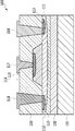
- FIG. 1 shows the structure of a conventional waveguide-coupled vertical GePD.
- FIG. 2 is a sectional view taken along the line II-II in FIG.
- the vertical GePD 100 is formed on a SOI (Silicon On Insulator) substrate including a Si substrate, a Si oxide film, and a surface Si layer by using a lithography technique or the like.
- the vertical GePD 100 includes a Si substrate 101, a lower clad layer 102 made of a Si oxide film on the Si substrate, a core layer 110 for guiding signal light, and a Ge layer 114 for absorbing light formed on the core layer 110. And an upper clad layer 103 formed on the core layer 110 and the Ge layer 114.
- the core layer 110 is divided into a waveguide layer 141 and a silicon slab 142.
- the silicon slab 142 is formed with the p-type Si slab 111 doped with the first conductivity type impurity ions, and the silicon electrode portions 112 and 113 functioning as electrodes by being doped with the first conductivity type impurity ions at a high concentration. ing.
- the Ge layer 114 is stacked by epitaxial growth, and the Ge region 115 doped with the second conductivity type impurity ions is formed on the top thereof.
- the Ge layer 114 may be a germanium compound. Electrodes 116 to 118 are provided on the silicon electrode portions 112 and 113 and the Ge region 115 so as to be in contact with them.
- the cladding layer 103 is omitted, and the electrodes 116 to 118 are shown only at positions in contact with the silicon electrode portions 112 and 113 and the Ge region 115.
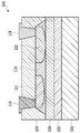
- FIG. 3 shows a first example of a conventional waveguide-coupled lateral GePD.
- a germanium region 121 doped with a first conductivity type impurity ion and a germanium region doped with a second conductivity type impurity ion are used.
- a region 122 is used in the lateral GePD 100.
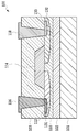
- FIG. 4 shows a second example of a conventional waveguide-coupled lateral GePD.
- lateral GePD 100 instead of the p-type Si slab 111 and the Ge region 115 shown in FIG. 2, a silicon region 131 doped with a first conductivity type impurity ion and a silicon region doped with a second conductivity type impurity ion are used.
- the region 132 and the silicon electrode portion 133 which is highly doped with the second impurity and acts as an electrode are provided.
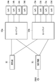
- FIG. 5 shows an example of the configuration of a receiver used in the optical digital coherent communication technology.
- This is a receiver of the polarization multiplexing 4-value phase modulation (DP-QPSK) system, and the received light is separated by a polarization separator 11 into two polarizations orthogonal to each other.
- DP-QPSK polarization multiplexing 4-value phase modulation
- each of the two polarized waves is caused to interfere with the local oscillation light from the local oscillation light source 12 to detect intensity and phase information, and two sets of differential signals are respectively generated by the four GePDs 14 and 15. It is converted into an electrical signal.
- temperature control is performed in such a receiver, it is necessary to provide a heater in each of the Ge PDs 14 and 15.
- GePDs connected to the same optical hybrid receive differential signals in pairs, so that the paired GePDs are required to have uniform sensitivity.
- FIG. 6 shows the temperature and wavelength dependence characteristics of the sensitivity of the conventional GePD.
- the conventional GePD has a characteristic that the temperature characteristic of sensitivity is not constant.
- the sensitivity is a characteristic of current output with respect to optical input power, and is a unit A/W.
- FIG. 6 is a graph plotting the sensitivity with respect to temperature in the C and L bands (wavelengths 1530 to 1565 nm, 1565 to 1625 nm) of the communication wavelength band when a reverse bias of 1.6 V is applied to GePD.
- the sensitivity is almost constant up to near the C band, but the sensitivity drops at the L band. This change in sensitivity is caused by a change in the optical absorption spectrum of germanium.
- sensitivity tends to decrease even in the C band.
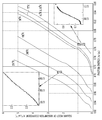
- Figure 7 shows the temperature dependence of the optical absorption spectrum of Ge.
- the horizontal axis is the photon energy, and the vertical axis is the square root of the absorption coefficient (see Non-Patent Document 1, for example).
- the band gap of germanium shifts to the high energy side. That is, the light absorption spectrum edge shifts to the short wavelength side.
- the light absorption spectrum edge of germanium used for GePD is at 1565 nm on the long wavelength side of the C band at 31°C. Therefore, even at a temperature of 31° C., even if the GePD has a constant sensitivity in the entire C band, the sensitivity gradually decreases from the long wavelength side as the temperature decreases. This tendency is shown in FIG. 6, where the sensitivity tends to decrease at ⁇ 5° C., which is the lower temperature for longer wavelengths.
- FIG. 8 shows a first example in which a heater is incorporated in a conventional GePD.
- a heater may be incorporated as a temperature control means.
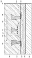
- the heater 130 made of a metal or a metal compound is incorporated in the upper cladding layer 103 immediately above the GePD.
- FIG. 9 shows a second example in which a heater is incorporated in a conventional GePD.
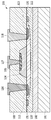
- a part of the GePD core layer 110 is doped with an impurity to form a resistor, thereby functioning as the heater 131.
- the heater 130 is warmed most efficiently when incorporated directly above the Ge layer 114.
- the width of the Ge layer 114 is defined as the length in the horizontal direction of FIG. 8, when the width of the heater 130 becomes larger than the width of the Ge layer 114, the electrodes overlap the electrodes 116 and 118. Since the electrodes 116 and 118 are made of a metal having thermal conductivity, heat escapes and the thermal efficiency given to the Ge layer 114 decreases.
- Fig. 10 shows the relationship between the heating value of the heater and the germanium temperature.
- the width of the Ge layer 114 is 8 ⁇ m and the width of the heater 130 is 3 ⁇ m (500), 8 ⁇ m (501), 9 ⁇ m (503), and 35 ⁇ m (502). It can be seen that when the width of the heater 130 exceeds the width of the Ge layer 114, the thermal efficiency drops.
- FIG. 11 shows the relationship between the germanium temperature and the heater width when the heating value of the heater is 40 mW. This is the relationship between the width of the heater 130 and the germanium temperature when the heating value of the heater is 40 mW.
- the heater width is 9 ⁇ m
- the germanium temperature is around 108° C., which is about 90% of that when the heater width is 3 ⁇ m or 8 ⁇ m. Therefore, it is preferable that the width of the heater 130 is equal to the width of the Ge layer 114, or larger by about 1 ⁇ m at the maximum.
- the length of the Ge layer 114 is defined as the length in the horizontal direction (the direction of the optical axis) of FIG.
- the length of the heater 130 is equal to the length of the Ge layer 114 or larger by at most about 1 ⁇ m.
- the thermal efficiency will decrease.
- the dimensions of the Ge layer 114 are about 1 to 10 ⁇ m in width and 10 to 50 ⁇ m in length.
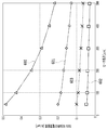
- FIG. 12 shows the relationship between the heater length and the current density when 500 V is applied. The results are shown when the width of the heater 130 in the GePD 100 is 3 ⁇ m (600), 8 ⁇ m (601), 16 ⁇ m (603), and 35 ⁇ m (602).
- the voltage of 500 V is a voltage generally required as the ESD withstand voltage in the human body model. Although it depends on the material and thickness of the heater, it is generally said that the breakdown due to ESD occurs when the current density reaches 150 to 250 mA/ ⁇ m 2 .
- the width of the heater 130 is 3 ⁇ m and the length of the heater 130 is 500 ⁇ m or less, the current density of 150 to 250 mA/ ⁇ m 2 or less cannot be exceeded, and a sufficient ESD withstand voltage cannot be obtained.
- the heater width of the heater 130 is 8 ⁇ m, when the length of the heater 130 is 300 ⁇ m or more, the current density approaches 150 to 250 mA/ ⁇ m 2 or less. Therefore, it can be said that the heater width is a border line that can ensure the ESD breakdown voltage.
- the heater 130 has a current density of 100 to 250 mA/ ⁇ m 2 or less and a sufficient ESD withstand voltage regardless of the length of the heater 130.
- the size of the heater that efficiently gives heat is about 1 to 10 ⁇ m in width and about 10 to 50 ⁇ m in length. From the results of FIG. 12, it is understood that a sufficient ESD withstand voltage cannot be ensured within this size range.
- An object of the present invention is to provide a GePD that does not have temperature dependence of sensitivity in the C and L bands by using a heater, and to provide a photodetector having a sufficient ESD withstand voltage.
- the present invention provides an embodiment of a photodetector, which comprises a plurality of photodiodes having germanium or a germanium compound in a light absorption layer, and a light absorption layer of each of the plurality of photodiodes.
- a plurality of heaters that apply heat to the plurality of heaters, the plurality of heaters being connected in series, being connected in parallel, or being a plurality of sets in which a plurality of heaters are connected in series are connected in parallel. It is characterized by
- the heater length can be regarded as the sum of the heater lengths
- the heater width can be regarded as the sum of the heater widths.
- the ESD withstand voltage which is determined by the width and the length, can be improved for the photodetector as a whole.
- FIG. 13 shows a photodetector according to an embodiment of the present invention.
- Each of the GePDs 200 to 203 includes heaters 210 to 213, and the heaters 210 to 213 are connected in series and connected to the power supplies 220 and 221.
- the heaters 210 and 211 are divided into the heaters 212 and 213, and a plurality of sets of a plurality of heaters connected in series are connected to the power supplies 220 and 221. Since a plurality of heaters are connected in series as seen from the power source, the heater length can be regarded as the sum of the heater lengths, and the heater width can be regarded as the sum of the heater widths. Therefore, even if the size of the heater included in one GePD is approximately the same as the size of the Ge layer 114, the ESD withstand voltage determined by the width and length of the heater can be improved for the entire photodetector.
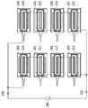
- FIG. 14 shows a photodetector according to the first embodiment of the present invention.
- Each of the GePDs 200 to 207 includes heaters 210 to 217, and the heaters 210 to 217 are connected in series and connected to the power supply 220.
- the heaters 210 to 217 are made of a metal or metal compound embedded in the upper cladding layer 103, as shown in FIG.
- the size of the heater is preferably about the same as the Ge layer 114.
- the dimensions of the Ge layer 114 are about 1 to 10 ⁇ m in width and 10 to 50 ⁇ m in length, and are 10 ⁇ 50 ⁇ m in the first embodiment. Referring to FIG. 12, one heater cannot reach a current density of 150 to 250 mA/ ⁇ m 2 or less, but by connecting eight heaters in series, the total heater length becomes 400 ⁇ m. A current density of 150 to 250 mA/ ⁇ m 2 or less can be satisfied.
- the heaters 210 to 217 connected in series are connected to the power supply 220 via terminals 230 and 231. These two terminals are the terminals to which the ESD load is applied, and are distributed to the heaters provided in the eight GePDs. Therefore, even if one heater is small, a sufficient ESD breakdown voltage can be obtained in the entire photodetector.
- FIG. 15 shows a photodetector according to the second embodiment of the present invention.
- Each of the GePDs 200 and 201 includes heaters 210 and 211, and the heaters 210 and 211 are connected in parallel and connected to the power supply 220.
- the heaters 210 and 211 are made of a metal or a metal compound embedded in the upper cladding layer 103, as shown in FIG.
- the size of the heater is preferably about the same as the Ge layer 114.
- the dimensions of the Ge layer 114 are about 1 to 10 ⁇ m in width and 10 to 50 ⁇ m in length, and are 10 ⁇ 50 ⁇ m in the second embodiment. Referring to FIG. 12, one heater cannot reach a current density of 150 to 250 mA/ ⁇ m 2 or less, but by connecting two heaters in parallel, the total heater width becomes 20 ⁇ m. A current density of up to 250 mA/ ⁇ m 2 can be satisfied.
- the heaters 210 and 211 connected in series are connected to the power supply 220 via terminals 230 and 231. Only these two terminals receive the ESD load, and the heaters provided in the two GePDs are dispersed and applied. Therefore, even if one heater is small, a sufficient ESD breakdown voltage can be obtained in the entire photodetector.
- FIG. 16 shows a photodetector according to the third embodiment of the present invention.
- Each of the GePDs 200 to 207 includes heaters 210 to 217, the heaters 210 to 213 and the heaters 214 to 217 are connected in series, and two sets of heaters are connected in parallel to the power supply 220.
- the heaters 210 to 217 are made of a metal or metal compound embedded in the upper cladding layer 103, as shown in FIG.
- the size of the heater is preferably about the same as the Ge layer 114.
- the dimensions of the Ge layer 114 are about 1 to 10 ⁇ m in width and 10 to 50 ⁇ m in length, and are 10 ⁇ 50 ⁇ m in the second embodiment. Referring to FIG. 12, one heater cannot reach a current density of 150 to 250 mA/ ⁇ m 2 or less, but by connecting two heaters in parallel, the total heater width is 20 ⁇ m and the heater length is Is 200 ⁇ m, so that a current density of 150 to 250 mA/ ⁇ m 2 or less can be satisfied.
- the heaters 210 to 213 and the heaters 214 to 217 connected in series are connected to the power supply 220 via terminals 230 and 231. Only these two terminals receive the ESD load, and the heaters provided in the two GePDs are dispersed and applied. Therefore, even if one heater is small, a sufficient ESD breakdown voltage can be obtained in the entire photodetector. Further, as compared with the second embodiment, the series resistance of each set of heaters increases and the resistance value can be increased, so that equivalent heat can be applied with a small voltage.
- FIG. 17 shows a photodetector according to the fourth embodiment of the present invention.
- Each of the GePDs 200 to 203 includes heaters 210 to 213, and the heaters 210 to 213 are connected in series and connected to the power supply 220. Further, the heaters 210 to 213 are respectively connected with capacitors 240 to 243 in parallel.
- the heaters 210 to 213 are made of a metal or metal compound embedded in the upper cladding layer 103, as shown in FIG.
- the size of the heater is preferably about the same as the Ge layer 114.
- the dimensions of the Ge layer 114 are about 1 to 10 ⁇ m in width and 10 to 50 ⁇ m in length, and are 10 ⁇ 50 ⁇ m in the fourth embodiment.
- one heater cannot reach a current density of 150 to 250 mA/ ⁇ m 2 or less, but by connecting four heaters in series, the total heater length becomes 200 ⁇ m.
- the capacitors 240 to 243 connected in parallel can satisfy a current density of 150 to 250 mA/ ⁇ m 2 or less. This is because the ESD load due to the capacity can be dispersed in addition to the serial connection of the heaters.
- the heaters 210 to 213 connected in series are connected to the power supply 220 via terminals 230 and 231. These two terminals are the terminals to which the ESD load is applied, and are distributed to the heaters provided in the eight GePDs. Therefore, even if one heater is small, a sufficient ESD breakdown voltage can be obtained in the entire photodetector.
- the configuration of the fourth embodiment is useful when the number of heaters is small and the current density cannot be sufficiently reduced even when connected in parallel or in series.
Landscapes
- Light Receiving Elements (AREA)
- Optical Integrated Circuits (AREA)
Abstract
十分なESD耐圧を備えた光検出器を提供する。光検出器の一実施態様は、ゲルマニウムまたはゲルマニウム化合物を光吸収層に有する複数のフォトダイオード(200,201,202,203)と、前記複数のフォトダイオード(200,201,202,203)の各々の光吸収層に熱を与える複数のヒータ(210,211,212,213)とを備え、前記複数のヒータ(210,211,212,213)は、直列に接続されるか、並列に接続されるか、または複数のヒータが直列に接続された組が複数並列に接続されている。
Description
本発明は、光検出器に関し、より詳細には、光通信システム、光情報処理システム等において用いられ、差動信号を受信するときの同相信号除去比が小さい光検出器に関する。
近年の光通信の普及に伴い、光通信装置の低コスト化が求められている。その解決策の1つとして、光通信装置を構成する光回路を、大口径のシリコンウエハ上に、シリコンフォトニクスによる微小光回路技術を用いて形成する方法が知られている。これにより、1チップあたりの材料費を劇的に下げ、光通信装置の低コスト化を図ることができる。このような技術を用いて、シリコン(Si)基板上に形成された光検出器として、モノリシック集積が可能なゲルマニウム光検出器(GePD)がある。
図1に、従来の導波路結合型の縦型GePDの構造を示す。図2は、図1の符号II-IIにおける断面図である。縦型のGePD100は、Si基板、Si酸化膜、表面Si層からなるSOI(Silicon On Insulator)基板にリソグラフィ技術等を用いて形成される。縦型のGePD100は、Si基板101と、Si基板上のSi酸化膜からなる下部クラッド層102と、信号光を導くコア層110と、コア層110上に形成された光を吸収するGe層114と、コア層110およびGe層114上に形成された上部クラッド層103を備えている。コア層110は、導波路層141とシリコンスラブ142に分けられる。
シリコンスラブ142は、第一の導電型不純物イオンがドーピングされたp型Siスラブ111、および第一の導電型不純物イオンが高濃度にドーピングされ、電極として作用するシリコン電極部112、113が形成されている。Ge層114は、エピタキシャル成長によって積層され、その上部に第二の導電型不純物イオンがドーピングされたGe領域115が形成されている。Ge層114は、ゲルマニウム化合物であることもある。シリコン電極部112、113およびGe領域115上には、それらに接するように電極116~118を備えている。
なお、構造を分かり易くするために、図1では、クラッド層103を省き、電極116~118は、シリコン電極部112、113およびGe領域115に接する位置のみを示している。
縦型のGePD100は、導波路層141からシリコンスラブ142に光が入射され、Ge層114で光が吸収されると、電極117と電極116、118との間に光電流が流れる。この光電流を検出することにより光を検出する。
図3に、従来の導波路結合型の横型GePDの第1例を示す。横型のGePD100は、図2に示したp型Siスラブ111とGe領域115の代わりに、第一の導電型不純物イオンがドーピングされたゲルマニウム領域121と第二の導電型不純物イオンがドーピングされたゲルマニウム領域122とを備えている。
図4に、従来の導波路結合型の横型GePDの第2例を示す。横型のGePD100は、図2に示したp型Siスラブ111とGe領域115の代わりに、第一の導電型不純物イオンがドーピングされたシリコン領域131と第二の導電型不純物イオンがドーピングされたシリコン領域132と、第二の不純物が高濃度にドーピングされ、電極として作用するシリコン電極部133とを備えている。
図5に、光デジタルコヒーレント通信技術において用いる受信機の構成の一例を示す。偏波多重4値位相変調(DP-QPSK)方式の受信機であり、受信光は偏波分離器11により直交する2つの偏波に分離される。2つの偏波のそれぞれを、光ハイブリッド13a,13bにおいて、局発光源12からの局発光と干渉させ、強度と位相の情報が検出され、それぞれ2組の差動信号が4つのGePD14,15により電気信号に変換される。このような受信機において、温度制御を行う場合には、GePD14,15のそれぞれにヒータを備える必要がある。特に、同一の光ハイブリッドに接続されるGePDは、2つ一組で差動信号を受信することから、ペアとなるGePDは、均一の感度が求められる。
Macfarlane G. G., T. P. McLean, J. E. Quarrington and V. Roberts, "fine Structure in the Absorption-Edge Spectrum of Ge," Physical Review vol.108, No.6 (1957) p.1377-1383.
図6に、従来のGePDの感度の温度および波長依存特性を示す。従来のGePDは、感度の温度特性が一定ではないという特性がある。ここで、感度とは、光入力パワーに対する電流出力の特性であり、単位A/Wである。図6は、GePDに逆バイアス1.6Vを与えたとき、通信波長帯域のC、L帯(波長1530~1565nm、1565~1625nm)における温度に対する感度をプロットした図である。例えば、31℃ではC帯付近まではほぼ一定の感度を示すが、L帯になると感度が落ちてしまう。この感度変化は、ゲルマニウムの光吸収スペクトルの変化によってもたらされている。-5℃になるとC帯においても感度を落とす傾向を示す。
図7に、Geの光吸収スペクトルの温度依存特性を示す。横軸はフォトンエネルギー、縦軸は吸収係数の平方根である(例えば、非特許文献1参照)。温度が低温になるとゲルマニウムのバンドギャップは、高エネルギー側にシフトする。すなわち、光吸収スペクトル端は短波長側にシフトする。GePDに用いているゲルマニウムの光吸収スペクトル端は、31℃でちょうどC帯の長波長側の1565nm付近にある。従って、31℃ではC帯全域に一定の感度を示すGePDであっても、温度が低くなるにつれ、長波長側から徐々に感度が落ちてゆく。この傾向を示したのが図6であり、長波長ほど低温である-5℃において感度を落とす傾向がある。
温度、波長によって感度が変化するGePDを光通信システムに組み込むためには、感度変化を補償する回路が必要となるため、製造コストが上がる。これを解決する手段として、GePDに印加する電圧を、温度、波長に応じて制御する手段がある(例えば、特許文献1~3参照)。
図8に、従来のGePDにヒータを組み込んだ第1例を示す。GePDの温度依存性を補償するたに、温度制御手段としてヒータを組み込む場合がある。第1例では、GePDの直上の上部クラッド層103の中に、金属または金属化合物で作製されたヒータ130を組み入れる。
図9に、従来のGePDにヒータを組み込んだ第2例を示す。第2例では、GePDのコア層110の一部に不純物をドーピングして、抵抗体とすることにより、ヒータ131として機能させる。
図8に示した第1例の場合、ヒータ130は、Ge層114の直上に組み入れる場合が最も熱効率良く温められる。Ge層114の幅を、図8の水平方向の長さと定義したとき、ヒータ130の幅がGe層114の幅より大きくなると、電極116,118に重なるようになる。電極116,118は、熱伝導性の金属であるため、熱が逃げ、Ge層114に与える熱効率が落ちてしまう。
図10に、ヒータ発熱量に対するゲルマニウム温度の関係を示す。GePD100においてGe層114の幅を8μmとし、ヒータ130の幅を3μm(500)、8μm(501)、9μm(503)、35μm(502)としたときのヒータ発熱量とゲルマニウム温度の関係である。ヒータ130の幅がGe層114の幅を超えると、熱効率が落ちていることがわかる。
図11に、ヒータ発熱量を40mWとした時のヒータ幅に対するゲルマニウム温度の関係を示す。ヒータの発熱量を40mWとしたとき、ヒータ130の幅に対するゲルマニウム温度の関係である。ヒータの幅が9μmになるとゲルマニウム温度は108℃付近を示し、ヒータの幅が3μmまたは8μmのときの90%程度である。従って、ヒータ130の幅は、Ge層114の幅と同等か、最大でも1μm程度大きいサイズにすることが好ましい。同様に、Ge層114の長さを、図1の水平方向(光軸の方向)の長さと定義したとき、ヒータ130の長さがGe層114の長さより大きくなるときも、熱効率が落ちてしまう。従って、ヒータ130の長さも、Ge層114の長さと同等か、最大でも1μm程度大きいサイズにすることが好ましい。
上述したように、ヒータ130は、Ge層114よりも大きな面積を有すると熱効率が落ちてしまう。一般的に、上述した受信機の通信速度で動作させるためには、Ge層114の寸法は、幅1~10μm、長さ10~50μm程度である。熱効率が落ちないように、このGe層114と同等のサイズのヒータ130を作製した場合、静電気放電(ESD:electro-static discharge)に弱くなるという問題がある。
図12に、ヒータの長さに対する500V印加時の電流密度の関係を示す。GePD100においてヒータ130の幅を3μm(600)、8μm(601)、16μm(603)、35μm(602)としたときの結果を示している。電圧500Vは、一般的に人体モデルにおけるESD耐圧として求められる電圧である。ヒータの材料や厚さにも依存するが、一般的に、電流密度が150~250mA/μm2に達したとき、ESDによる破壊が起きるとされている。ヒータ130の幅が3μmの場合、ヒータ130の長さが500μm以下のでは、150~250mA/μm2以下の電流密度を下回ることができず、十分なESD耐圧を持つことができない。
ヒータ130の幅が8μmの場合、ヒータ130の長さが300μm以上で150~250mA/μm2以下の電流密度に近づく。このため、ESD耐圧を確保することができるボーダーラインのヒータ幅と言える。ヒータ130の幅が35μmおよび16μmの場合、ヒータ130の長さがどの値であっても100~250mA/μm2以下の電流密度を有し、十分なESD耐圧を持つことができる。
例えば、GePD100のGe層114のサイズが、幅1~10μm、長さ10~50μm程度のとき、効率的に熱を与えるヒータの寸法は、幅1~10μm、長さ10~50μm程度になるが、図12の結果から、この寸法範囲では十分なESD耐圧を確保できないことがわかる。
本発明の目的は、ヒータを用いることにより、C、L帯において感度の温度依存性のないGePDを提供し、十分なESD耐圧を備えた光検出器を提供することにある。
本発明は、このような目的を達成するために、光検出器の一実施態様は、ゲルマニウムまたはゲルマニウム化合物を光吸収層に有する複数のフォトダイオードと、前記複数のフォトダイオードの各々の光吸収層に熱を与える複数のヒータとを備え、前記複数のヒータは、直列に接続されるか、並列に接続されるか、または複数のヒータが直列に接続された組が複数並列に接続されていることを特徴とする。
本発明によれば、複数のヒータが直列または並列に接続されているので、ヒータの長さは各ヒータ長さの和として、ヒータの幅は各ヒータ幅の和としてみなすことができ、ヒータの幅と長さから決まるESD耐圧は、光検出器全体としては向上させることができる。
以下、図面を参照しながら本発明の実施形態について詳細に説明する。
図13に、本発明の一実施形態にかかる光検出器を示す。GePD200~203の各々は、ヒータ210~213を備え、ヒータ210~213が直列に接続されて電源220,221に接続されている。ここでは、ヒータ210,211とヒータ212,213とに分けて、直列に接続された複数のヒータが複数組、電源220,221に接続されている構成である。電源から見て複数のヒータが直列に接続されているので、ヒータの長さは各ヒータ長さの和として、ヒータの幅は各ヒータ幅の和としてみなすことができる。従って、1つのGePDに備えられるヒータのサイズがGe層114のサイズと同程度であっても、ヒータの幅と長さから決まるESD耐圧は、光検出器全体としては向上させることができる。
図14に、本発明の実施例1にかかる光検出器を示す。GePD200~207の各々は、ヒータ210~217を備え、ヒータ210~217が直列に接続されて電源220に接続されている。ヒータ210~217は、図8に示したように、上部クラッド層103の中に埋め込まれた金属または金属化合物によって作られている。
ヒータのサイズは、Ge層114と同程度のサイズであることが望ましい。Ge層114の寸法は、幅1~10μm、長さ10~50μm程度であり、実施例1では10x50μmとする。図12を参照すると、1つのヒータでは150~250mA/μm2 以下の電流密度に達することができないが、8つのヒータを直列に接続することにより、トータルのヒータの長さは400μmとなるため、150~250mA/μm2以下の電流密度を満たすことができる。
直列に接続されたヒータ210~217は、端子230,231を介して電源220に接続されている。ESD負荷がかかる端子はこの2つの端子だけであり、8個のGePDに設けたヒータには分散してかかる。従って、1つのヒータが小さくても、光検出器全体では十分なESD耐圧を獲得することができる。
図15に、本発明の実施例2にかかる光検出器を示す。GePD200,201の各々は、ヒータ210,211を備え、ヒータ210,211が並列に接続されて電源220に接続されている。ヒータ210,211は、図8に示したように、上部クラッド層103の中に埋め込まれた金属または金属化合物によって作られている。
ヒータのサイズは、Ge層114と同程度のサイズであることが望ましい。Ge層114の寸法は、幅1~10μm、長さ10~50μm程度であり、実施例2では10x50μmとする。図12を参照すると、1つのヒータでは150~250mA/μm2 以下の電流密度に達することができないが、2つのヒータを並列に接続することにより、トータルのヒータの幅は20μmとなるため、150~250mA/μm2以下の電流密度を満たすことができる。
直列に接続されたヒータ210,211は、端子230,231を介して電源220に接続されている。ESD負荷がかかる端子はこの2つの端子だけであり、2個のGePDに設けたヒータにも分散してかかる。従って、1つのヒータが小さくても、光検出器全体では十分なESD耐圧を獲得することができる。
図16に、本発明の実施例3にかかる光検出器を示す。GePD200~207の各々は、ヒータ210~217を備え、ヒータ210~213とヒータ214~217のそれぞれが直列に接続され、2組のヒータが並列に電源220に接続されている。ヒータ210~217は、図8に示したように、上部クラッド層103の中に埋め込まれた金属または金属化合物によって作られている。
ヒータのサイズは、Ge層114と同程度のサイズであることが望ましい。Ge層114の寸法は、幅1~10μm、長さ10~50μm程度であり、実施例2では10x50μmとする。図12を参照すると、1つのヒータでは150~250mA/μm2 以下の電流密度に達することができないが、2つのヒータを並列に接続することにより、トータルのヒータの幅は20μm、ヒータの長さは200μmとなるため、150~250mA/μm2以下の電流密度を満たすことができる。
直列に接続されたヒータ210~213とヒータ214~217とは、端子230,231を介して電源220に接続されている。ESD負荷がかかる端子はこの2つの端子だけであり、2個のGePDに設けたヒータにも分散してかかる。従って、1つのヒータが小さくても、光検出器全体では十分なESD耐圧を獲得することができる。また、実施例2と比較すると、ヒータの各組の直列抵抗が増え、抵抗値を上げることができるので、小さい電圧で同等の熱を加えることができる。
図17に、本発明の実施例4にかかる光検出器を示す。GePD200~203の各々は、ヒータ210~213を備え、ヒータ210~213が直列に接続されて電源220に接続されている。さらに、ヒータ210~213には、容量240~243がそれぞれ並列に接続されている。ヒータ210~213は、図8に示したように、上部クラッド層103の中に埋め込まれた金属または金属化合物によって作られている。
ヒータのサイズは、Ge層114と同程度のサイズであることが望ましい。Ge層114の寸法は、幅1~10μm、長さ10~50μm程度であり、実施例4では10x50μmとする。図12を参照すると、1つのヒータでは150~250mA/μm2 以下の電流密度に達することができないが、4つのヒータを直列に接続することにより、トータルのヒータの長さは200μmとなり、加えて並列に接続された容量240~243により、150~250mA/μm2以下の電流密度を満たすことができる。ヒータの直列化に加えて、容量によるESD負荷を分散させることができるからである。
直列に接続されたヒータ210~213は、端子230,231を介して電源220に接続されている。ESD負荷がかかる端子はこの2つの端子だけであり、8個のGePDに設けたヒータには分散してかかる。従って、1つのヒータが小さくても、光検出器全体では十分なESD耐圧を獲得することができる。ヒータの数が少なく、並列または直列に接続した場合でも、十分に電流密度を下げることができなかった場合に、実施例4の構成は有用である。
100,200~207 GePD
101 Si基板
102 下部クラッド層
103 上部クラッド層
110 コア層
111 p型Siスラブ
112、113,133 シリコン電極部
114 Ge層
115 Ge領域
116~118 電極
121,122 ゲルマニウム領域
130,210~217 ヒータ
131,132 シリコン領域
141 導波路層
142 シリコンスラブ
220,221 電源
230,231 端子
240~243 容量
101 Si基板
102 下部クラッド層
103 上部クラッド層
110 コア層
111 p型Siスラブ
112、113,133 シリコン電極部
114 Ge層
115 Ge領域
116~118 電極
121,122 ゲルマニウム領域
130,210~217 ヒータ
131,132 シリコン領域
141 導波路層
142 シリコンスラブ
220,221 電源
230,231 端子
240~243 容量
Claims (8)
- ゲルマニウムまたはゲルマニウム化合物を光吸収層に有する複数のフォトダイオードと、
前記複数のフォトダイオードの各々の光吸収層に熱を与える複数のヒータとを備え、
前記複数のヒータは、直列に接続されるか、並列に接続されるか、または複数のヒータが直列に接続された組が複数並列に接続されていることを特徴とする光検出器。 - 前記フォトダイオードは、
シリコン基板と、
前記シリコン基板上に形成された下部クラッド層と、
前記下部クラッド層上に形成され、第一の導電型不純物イオンがドーピングされたシリコンスラブ、前記第一の導電型不純物イオンが高濃度にドーピングされた電極部、および前記シリコンスラブに接続された導波路層を含むコア層と、
前記コア層上に形成され、第二の導電型不純物がドーピングされたゲルマニウム領域を含むゲルマニウム層と、
前記コア層および前記ゲルマニウム層上に形成された上部クラッド層と、
前記電極部および前記ゲルマニウム領域にそれぞれ接続された電極と
を含むことを特徴とする請求項1に記載の光検出器。 - 前記フォトダイオードは、
シリコン基板と、
前記シリコン基板上に形成された下部クラッド層と、
前記下部クラッド層上に形成され、第一の導電型不純物イオンがドーピングされたシリコンスラブ、および前記シリコンスラブに接続された導波路層を含むコア層と、
前記コア層上に形成され、第一の導電型不純物イオンがドーピングされた第一のゲルマニウム領域、および第二の導電型不純物イオンがドーピングされた第二のゲルマニウム領域を含むゲルマニウム層と、
前記コア層および前記ゲルマニウム層上に形成された上部クラッド層と、
前記第一および前記第二のゲルマニウム領域にそれぞれ接続された電極と
を含むことを特徴とする請求項1に記載の光検出器。 - 前記フォトダイオードは、
シリコン基板と、
前記シリコン基板上に形成された下部クラッド層と、
前記下部クラッド層上に形成され、第一の導電型不純物イオンがドーピングされた第一のシリコン領域および前記第一の導電型不純物イオンがドーピングされた第一の電極部、並びに、第二の導電型不純物イオンがドーピングされた第二のシリコン領域、および前記第二の導電型不純物イオンがドーピングされた第二の電極部を含むシリコンスラブと、前記シリコンスラブに接続された導波路層とを含むコア層と、
前記コア層上に形成されたゲルマニウム層と、
前記コア層および前記ゲルマニウム層上に形成された上部クラッド層と、
前記第一および前記第二の電極部に接続された電極と
を含むことを特徴とする請求項1に記載の光検出器。 - 前記ヒータは、前記上部クラッド層の中に埋め込まれた金属または金属化合物からなり、前記光吸収層の直上に配置され、
前記ヒータの幅と長さは、前記光吸収層の幅と長さにそれぞれ等しいか、1μm大きいことを特徴とする請求項2、3または4に記載の光検出器。 - 前記ヒータは、前記コア層に不純物をドーピングして作製され、前記光吸収層の周囲に配置されることを特徴とする請求項2、3または4に記載の光検出器。
- 前記ヒータの各々に流れる電流密度が150~250mA/μm2以下となることを特徴とする請求項5または6に記載の光検出器。
- 前記ヒータと並列に接続された容量をさらに備えたことを特徴とする請求項5または6に記載の光検出器。
Priority Applications (1)
| Application Number | Priority Date | Filing Date | Title |
|---|---|---|---|
| US17/422,037 US12119419B2 (en) | 2019-01-16 | 2020-01-15 | Photodetector |
Applications Claiming Priority (2)
| Application Number | Priority Date | Filing Date | Title |
|---|---|---|---|
| JP2019-005496 | 2019-01-16 | ||
| JP2019005496A JP7208494B2 (ja) | 2019-01-16 | 2019-01-16 | 光検出器 |
Publications (1)
| Publication Number | Publication Date |
|---|---|
| WO2020149277A1 true WO2020149277A1 (ja) | 2020-07-23 |
Family
ID=71613034
Family Applications (1)
| Application Number | Title | Priority Date | Filing Date |
|---|---|---|---|
| PCT/JP2020/000955 Ceased WO2020149277A1 (ja) | 2019-01-16 | 2020-01-15 | 光検出器 |
Country Status (3)
| Country | Link |
|---|---|
| US (1) | US12119419B2 (ja) |
| JP (1) | JP7208494B2 (ja) |
| WO (1) | WO2020149277A1 (ja) |
Citations (6)
| Publication number | Priority date | Publication date | Assignee | Title |
|---|---|---|---|---|
| JP2002156536A (ja) * | 2000-11-17 | 2002-05-31 | Hitachi Cable Ltd | 導波路型光モジュール |
| US20150243800A1 (en) * | 2014-02-21 | 2015-08-27 | Sifotonics Technologies Co., Ltd. | Ge/Si Avalanche Photodiode With Integrated Heater And Fabrication Thereof |
| US20170092785A1 (en) * | 2015-09-24 | 2017-03-30 | Coriant Advanced Technology, LLC | Photodetector with integrated temperature control element |
| JP2018074104A (ja) * | 2016-11-04 | 2018-05-10 | 日本電信電話株式会社 | 光検出器 |
| JP2018082089A (ja) * | 2016-11-17 | 2018-05-24 | 日本電信電話株式会社 | 光検出器 |
| JP2018092983A (ja) * | 2016-11-30 | 2018-06-14 | 日本電信電話株式会社 | 光受信回路 |
Family Cites Families (4)
| Publication number | Priority date | Publication date | Assignee | Title |
|---|---|---|---|---|
| JP4945907B2 (ja) | 2005-03-03 | 2012-06-06 | 日本電気株式会社 | 波長可変レーザ |
| US7738517B2 (en) * | 2007-10-29 | 2010-06-15 | Avago Technologies Fiber Ip (Singapore) Pte. Ltd. | Small form factor transmitter optical subassembly (TOSA) having functionality for controlling the temperature, and methods of making and using the TOSA |
| JP2015153899A (ja) | 2014-02-14 | 2015-08-24 | 日本電信電話株式会社 | 受光素子の制御方法 |
| JP6981365B2 (ja) * | 2018-05-17 | 2021-12-15 | 日本電信電話株式会社 | 光検出器 |
-
2019
- 2019-01-16 JP JP2019005496A patent/JP7208494B2/ja active Active
-
2020
- 2020-01-15 WO PCT/JP2020/000955 patent/WO2020149277A1/ja not_active Ceased
- 2020-01-15 US US17/422,037 patent/US12119419B2/en active Active
Patent Citations (6)
| Publication number | Priority date | Publication date | Assignee | Title |
|---|---|---|---|---|
| JP2002156536A (ja) * | 2000-11-17 | 2002-05-31 | Hitachi Cable Ltd | 導波路型光モジュール |
| US20150243800A1 (en) * | 2014-02-21 | 2015-08-27 | Sifotonics Technologies Co., Ltd. | Ge/Si Avalanche Photodiode With Integrated Heater And Fabrication Thereof |
| US20170092785A1 (en) * | 2015-09-24 | 2017-03-30 | Coriant Advanced Technology, LLC | Photodetector with integrated temperature control element |
| JP2018074104A (ja) * | 2016-11-04 | 2018-05-10 | 日本電信電話株式会社 | 光検出器 |
| JP2018082089A (ja) * | 2016-11-17 | 2018-05-24 | 日本電信電話株式会社 | 光検出器 |
| JP2018092983A (ja) * | 2016-11-30 | 2018-06-14 | 日本電信電話株式会社 | 光受信回路 |
Also Published As
| Publication number | Publication date |
|---|---|
| US20220102561A1 (en) | 2022-03-31 |
| US12119419B2 (en) | 2024-10-15 |
| JP7208494B2 (ja) | 2023-01-19 |
| JP2020113716A (ja) | 2020-07-27 |
Similar Documents
| Publication | Publication Date | Title |
|---|---|---|
| US9893219B2 (en) | Graphene photodetector and graphene optical modulator | |
| JP6793786B1 (ja) | 半導体受光素子、光電融合モジュール及びアバランシェフォトダイオードの製造方法 | |
| CN107924961B (zh) | 光检测器 | |
| US9978890B1 (en) | Germanium multi-directional detector | |
| US11183603B2 (en) | Germanium photodetector with extended responsivity | |
| JP6646559B2 (ja) | 光検出器 | |
| CN101521244B (zh) | 半导体受光元件 | |
| JP6284195B2 (ja) | 受光素子 | |
| US11769849B2 (en) | Photodetector | |
| WO2020149277A1 (ja) | 光検出器 | |
| US11543293B2 (en) | Photodetector | |
| JP6362142B2 (ja) | ゲルマニウム受光器 | |
| JP2025501644A (ja) | グラフェン光検出器 | |
| US11887999B2 (en) | Photodetector | |
| JP6660338B2 (ja) | 光検出器 | |
| JP7081508B2 (ja) | 光検出器 | |
| WO2008042145A2 (en) | System and method for providing a high frequency response silicon photodetector | |
| US12087800B2 (en) | Photodector including germanium layer and doped region |
Legal Events
| Date | Code | Title | Description |
|---|---|---|---|
| 121 | Ep: the epo has been informed by wipo that ep was designated in this application |
Ref document number: 20741289 Country of ref document: EP Kind code of ref document: A1 |
|
| NENP | Non-entry into the national phase |
Ref country code: DE |
|
| 122 | Ep: pct application non-entry in european phase |
Ref document number: 20741289 Country of ref document: EP Kind code of ref document: A1 |