WO2020149037A1 - 非接触給電装置 - Google Patents
非接触給電装置 Download PDFInfo
- Publication number
- WO2020149037A1 WO2020149037A1 PCT/JP2019/047251 JP2019047251W WO2020149037A1 WO 2020149037 A1 WO2020149037 A1 WO 2020149037A1 JP 2019047251 W JP2019047251 W JP 2019047251W WO 2020149037 A1 WO2020149037 A1 WO 2020149037A1
- Authority
- WO
- WIPO (PCT)
- Prior art keywords
- coil
- power
- circuit
- resonance
- receiving
- Prior art date
- Legal status (The legal status is an assumption and is not a legal conclusion. Google has not performed a legal analysis and makes no representation as to the accuracy of the status listed.)
- Ceased
Links
Images



Classifications
-
- H—ELECTRICITY
- H02—GENERATION; CONVERSION OR DISTRIBUTION OF ELECTRIC POWER
- H02J—ELECTRIC POWER NETWORKS; CIRCUIT ARRANGEMENTS OR SYSTEMS FOR SUPPLYING OR DISTRIBUTING ELECTRIC POWER; SYSTEMS FOR STORING ELECTRIC ENERGY
- H02J50/00—Circuit arrangements or systems for wireless supply or distribution of electric power
- H02J50/80—Circuit arrangements or systems for wireless supply or distribution of electric power involving the exchange of data, concerning supply or distribution of electric power, between transmitting devices and receiving devices
-
- H—ELECTRICITY
- H02—GENERATION; CONVERSION OR DISTRIBUTION OF ELECTRIC POWER
- H02J—ELECTRIC POWER NETWORKS; CIRCUIT ARRANGEMENTS OR SYSTEMS FOR SUPPLYING OR DISTRIBUTING ELECTRIC POWER; SYSTEMS FOR STORING ELECTRIC ENERGY
- H02J50/00—Circuit arrangements or systems for wireless supply or distribution of electric power
- H02J50/10—Circuit arrangements or systems for wireless supply or distribution of electric power using inductive coupling
- H02J50/12—Circuit arrangements or systems for wireless supply or distribution of electric power using inductive coupling of the resonant type
-
- H—ELECTRICITY
- H02—GENERATION; CONVERSION OR DISTRIBUTION OF ELECTRIC POWER
- H02J—ELECTRIC POWER NETWORKS; CIRCUIT ARRANGEMENTS OR SYSTEMS FOR SUPPLYING OR DISTRIBUTING ELECTRIC POWER; SYSTEMS FOR STORING ELECTRIC ENERGY
- H02J50/00—Circuit arrangements or systems for wireless supply or distribution of electric power
- H02J50/005—Mechanical details of housing or structure aiming to accommodate the power transfer means, e.g. mechanical integration of coils, antennas or transducers into emitting or receiving devices
-
- H—ELECTRICITY
- H02—GENERATION; CONVERSION OR DISTRIBUTION OF ELECTRIC POWER
- H02M—APPARATUS FOR CONVERSION BETWEEN AC AND AC, BETWEEN AC AND DC, OR BETWEEN DC AND DC, AND FOR USE WITH MAINS OR SIMILAR POWER SUPPLY SYSTEMS; CONVERSION OF DC OR AC INPUT POWER INTO SURGE OUTPUT POWER; CONTROL OR REGULATION THEREOF
- H02M1/00—Details of apparatus for conversion
- H02M1/0048—Circuits or arrangements for reducing losses
-
- H—ELECTRICITY
- H02—GENERATION; CONVERSION OR DISTRIBUTION OF ELECTRIC POWER
- H02M—APPARATUS FOR CONVERSION BETWEEN AC AND AC, BETWEEN AC AND DC, OR BETWEEN DC AND DC, AND FOR USE WITH MAINS OR SIMILAR POWER SUPPLY SYSTEMS; CONVERSION OF DC OR AC INPUT POWER INTO SURGE OUTPUT POWER; CONTROL OR REGULATION THEREOF
- H02M1/00—Details of apparatus for conversion
- H02M1/0067—Converter structures employing plural converter units, other than for parallel operation of the units on a single load
- H02M1/007—Plural converter units in cascade
-
- H—ELECTRICITY
- H02—GENERATION; CONVERSION OR DISTRIBUTION OF ELECTRIC POWER
- H02M—APPARATUS FOR CONVERSION BETWEEN AC AND AC, BETWEEN AC AND DC, OR BETWEEN DC AND DC, AND FOR USE WITH MAINS OR SIMILAR POWER SUPPLY SYSTEMS; CONVERSION OF DC OR AC INPUT POWER INTO SURGE OUTPUT POWER; CONTROL OR REGULATION THEREOF
- H02M1/00—Details of apparatus for conversion
- H02M1/42—Circuits or arrangements for compensating for or adjusting power factor in converters or inverters
- H02M1/4208—Arrangements for improving power factor of AC input
- H02M1/4225—Arrangements for improving power factor of AC input using a non-isolated boost converter
-
- H—ELECTRICITY
- H02—GENERATION; CONVERSION OR DISTRIBUTION OF ELECTRIC POWER
- H02M—APPARATUS FOR CONVERSION BETWEEN AC AND AC, BETWEEN AC AND DC, OR BETWEEN DC AND DC, AND FOR USE WITH MAINS OR SIMILAR POWER SUPPLY SYSTEMS; CONVERSION OF DC OR AC INPUT POWER INTO SURGE OUTPUT POWER; CONTROL OR REGULATION THEREOF
- H02M3/00—Conversion of DC power input into DC power output
- H02M3/22—Conversion of DC power input into DC power output with intermediate conversion into AC
- H02M3/24—Conversion of DC power input into DC power output with intermediate conversion into AC by static converters
- H02M3/28—Conversion of DC power input into DC power output with intermediate conversion into AC by static converters using discharge tubes with control electrode or semiconductor devices with control electrode to produce the intermediate AC
- H02M3/325—Conversion of DC power input into DC power output with intermediate conversion into AC by static converters using discharge tubes with control electrode or semiconductor devices with control electrode to produce the intermediate AC using devices of a triode or a transistor type requiring continuous application of a control signal
- H02M3/335—Conversion of DC power input into DC power output with intermediate conversion into AC by static converters using discharge tubes with control electrode or semiconductor devices with control electrode to produce the intermediate AC using devices of a triode or a transistor type requiring continuous application of a control signal using semiconductor devices only
- H02M3/33569—Conversion of DC power input into DC power output with intermediate conversion into AC by static converters using discharge tubes with control electrode or semiconductor devices with control electrode to produce the intermediate AC using devices of a triode or a transistor type requiring continuous application of a control signal using semiconductor devices only having several active switching elements
- H02M3/33573—Full-bridge at primary side of an isolation transformer
-
- H—ELECTRICITY
- H02—GENERATION; CONVERSION OR DISTRIBUTION OF ELECTRIC POWER
- H02M—APPARATUS FOR CONVERSION BETWEEN AC AND AC, BETWEEN AC AND DC, OR BETWEEN DC AND DC, AND FOR USE WITH MAINS OR SIMILAR POWER SUPPLY SYSTEMS; CONVERSION OF DC OR AC INPUT POWER INTO SURGE OUTPUT POWER; CONTROL OR REGULATION THEREOF
- H02M7/00—Conversion of AC power input into DC power output; Conversion of DC power input into AC power output
- H02M7/02—Conversion of AC power input into DC power output without possibility of reversal
- H02M7/04—Conversion of AC power input into DC power output without possibility of reversal by static converters
- H02M7/06—Conversion of AC power input into DC power output without possibility of reversal by static converters using discharge tubes without control electrode or semiconductor devices without control electrode
-
- H—ELECTRICITY
- H04—ELECTRIC COMMUNICATION TECHNIQUE
- H04B—TRANSMISSION
- H04B5/00—Near-field transmission systems, e.g. inductive or capacitive transmission systems
- H04B5/70—Near-field transmission systems, e.g. inductive or capacitive transmission systems specially adapted for specific purposes
- H04B5/79—Near-field transmission systems, e.g. inductive or capacitive transmission systems specially adapted for specific purposes for data transfer in combination with power transfer
-
- Y—GENERAL TAGGING OF NEW TECHNOLOGICAL DEVELOPMENTS; GENERAL TAGGING OF CROSS-SECTIONAL TECHNOLOGIES SPANNING OVER SEVERAL SECTIONS OF THE IPC; TECHNICAL SUBJECTS COVERED BY FORMER USPC CROSS-REFERENCE ART COLLECTIONS [XRACs] AND DIGESTS
- Y02—TECHNOLOGIES OR APPLICATIONS FOR MITIGATION OR ADAPTATION AGAINST CLIMATE CHANGE
- Y02B—CLIMATE CHANGE MITIGATION TECHNOLOGIES RELATED TO BUILDINGS, e.g. HOUSING, HOUSE APPLIANCES OR RELATED END-USER APPLICATIONS
- Y02B70/00—Technologies for an efficient end-user side electric power management and consumption
- Y02B70/10—Technologies improving the efficiency by using switched-mode power supplies [SMPS], i.e. efficient power electronics conversion e.g. power factor correction or reduction of losses in power supplies or efficient standby modes
Definitions
- the present invention relates to a contactless power supply device.
- non-contact power feeding also called wireless power feeding
- a coil on a primary side (power transmission side) (hereinafter, referred to as a transmission coil) and a coil on a secondary side (power reception side) (hereinafter, referred to as a coil) , which is referred to as a receiving coil) is electromagnetically coupled with each other, so that power is transmitted from the power transmitting side device to the power receiving side device through the two coils.
- a transmission coil power transmission side
- a coil on a secondary side power reception side
- Patent Document 1 a resonance suppressing circuit including a control coil magnetically coupled to the power receiving resonance coil is provided on the power receiving side, the output voltage is monitored, and the resonance operation is performed by a method of short-circuiting and opening the control coil with a switch. It has been proposed to suppress.
- Patent Document 2 discloses that a secondary coil and a tertiary coil that are magnetically coupled to a primary coil included in a power feeding unit are provided, and a load is attached to the secondary coil.
- a contactless power supply device has been proposed that includes a power receiving unit that generates power to be supplied and has a resonance capacitor connected to a tertiary coil.
- the secondary coil and the tertiary coil are separately arranged and the tertiary coil is arranged on the front side closer to the primary coil than the secondary coil.
- the resonance operation of the power receiving resonance circuit including the power receiving resonance coil is sufficiently performed when there is no load circuit connected to the reception coil or when the current flowing through the load circuit is very small. In some cases, it may not be possible to suppress excessive increase in the voltage output from the power receiving resonance circuit. Further, in the technique disclosed in Patent Document 2, even when the degree of coupling between the tertiary coil and the primary coil to which the resonance capacitor is connected is extremely high, the resonance operation of the circuit including the tertiary coil is suppressed. Is not supposed.
- an object of the present invention is to provide a contactless power supply device that can suppress an excessive increase in the output voltage from the device on the power receiving side.
- a contactless power feeding device including a power transmitting device and a power receiving device to which power is transferred from the power transmitting device in a contactless manner.
- the power transmission device includes a transmission coil that transmits electric power to the power reception device, and a power supply circuit that supplies AC power to the transmission coil.
- the power receiving device includes a receiving coil that receives electric power from the power transmitting device, a resonant circuit that includes a resonant capacitor that is connected in series with the receiving coil, a rectifying circuit that rectifies the electric power received through the resonant circuit, and a receiving circuit.
- a resonance suppression coil that is electromagnetically coupled to the coil, a switch circuit that is connected to the resonance suppression coil, and that can switch the resonance suppression coil between short circuit and open circuit, and measure the output voltage of the power output from the rectifier circuit. It has a voltage detection circuit that obtains a measured value of the output voltage, and a determination circuit that controls the switch circuit to short-circuit the resonance suppression coil when the measured value of the output voltage becomes equal to or higher than a predetermined upper threshold value.
- the receiving coil and the resonance suppressing coil are arranged so that The non-contact power supply device according to the present invention can suppress the output voltage from the power receiving device from excessively rising by having such a configuration.
- the non-contact power supply device according to the present invention can suppress the output voltage from the power receiving device from excessively rising by having such a configuration.
- the resonance suppression coil is closer to the transmission coil than the reception coil. It is preferable that the receiving coil and the resonance suppressing coil are arranged. Accordingly, when the power transmitting device and the power receiving device are arranged so that power is transmitted from the transmitting coil to the receiving coil, the coupling degree between the resonance suppressing coil and the transmitting coil is more reliably determined between the receiving coil and the transmitting coil. Since it can be higher than the degree of coupling, the contactless power supply device can more reliably suppress an excessive increase in the output voltage from the device on the power receiving side.
- the resonance suppressing coil is positioned between the transmitting coil and the receiving coil so that the resonance suppressing coil is located between the receiving coil and the receiving coil.
- a resonance suppression coil is preferably arranged.
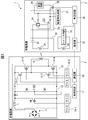
- FIG. 1 is a schematic configuration diagram of a contactless power supply device according to an embodiment of the present invention.
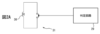
- FIG. 2A is a diagram illustrating an example of the switch circuit.
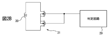
- FIG. 2B is a diagram showing another example of the switch circuit.
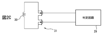
- FIG. 2C is a diagram showing still another example of the switch circuit.
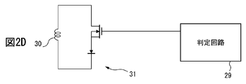
- FIG. 2D is a diagram showing still another example of the switch circuit.
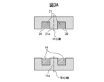
- FIG. 3A is a schematic cross-sectional view in a plane passing through the central axes of the transmission coil, the reception coil, and the resonance suppression coil.
- FIG. 3B is a schematic plan view of an example of the arrangement of the receiving coil and the resonance suppressing coil viewed from the transmitting coil side.
- FIG. 3A is a schematic cross-sectional view in a plane passing through the central axes of the transmission coil, the reception coil, and the resonance suppression coil.
- FIG. 3B is a schematic plan view of an example of the arrangement of the receiving coil and the resonance suppressing coil viewed from the transmitting
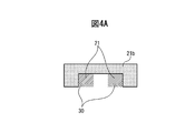
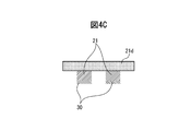
- FIG. 4A is a schematic cross-sectional view in a plane passing through the central axes of the reception coil and the resonance suppression coil according to the modification.
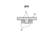
- FIG. 4B is a schematic cross-sectional view in a plane passing through the central axes of the receiving coil and the resonance suppressing coil according to another modification.
- FIG. 4C is a schematic cross-sectional view in a plane passing through the central axes of the reception coil and the resonance suppression coil according to another modification.
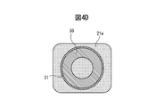
- FIG. 4D is a schematic plan view of another example of the arrangement of the reception coil and the resonance suppression coil viewed from the transmission coil side according to still another modification.
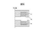
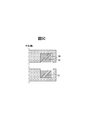
- FIG. 5A is a schematic cross-sectional view in a plane passing through the central axes of the transmission coil, the reception coil, and the resonance suppression coil according to the present embodiment.
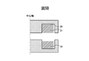
- FIG. 5B is a schematic cross-sectional view in a plane passing through the central axes of the transmission coil, the reception coil, and the resonance suppression coil according to the comparative example.
- FIG. 5C is a schematic cross-sectional view in a plane passing through the central axes of the transmission coil, the reception coil, and the resonance suppression coil according to the comparative example.
- FIG. 6 is a diagram showing an example of a simulation result of the frequency characteristic of the output voltage when the current flowing through the load circuit connected to the power receiving device is small.
- FIG. 7 is a figure which shows an example of the simulation result of the frequency characteristic of an output voltage when there exists a load connected to a power receiving apparatus.
- FIG. 8A is a schematic cross-sectional view showing a positional relationship between a receiving coil and a resonance suppressing coil according to a modification, in a plane passing through central axes of the receiving coil and the resonance suppressing coil.
- FIG. 8B is a schematic cross-sectional view showing a positional relationship between the reception coil and the resonance suppression coil according to the modification, in a plane passing through the central axes of the reception coil and the resonance suppression coil.
- the device on the power receiving side has a receiving coil for receiving power and a resonance suppressing coil (hereinafter, simply referred to as resonance suppressing coil) provided so as to be electromagnetically coupled to the receiving coil. ..
- resonance suppressing coil a resonance suppressing coil provided so as to be electromagnetically coupled to the receiving coil.
- this non-contact power supply device when the power transmission side device and the power reception side device are arranged so that power can be transmitted between the power transmission side device and the power reception side device, that is, the transmission coil and the reception coil. Resonance suppression so that the coupling degree between the transmission coil and the resonance suppression coil is higher than the coupling degree between the transmission coil and the reception coil when the two devices are arranged so as to be electromagnetically coupled with the coil.
- a coil and a receiving coil are arranged.
- this contactless power supply device has no load circuit connected to the device on the power receiving side, or when the current flowing through the load circuit is very small (for example, the load circuit is a secondary battery, and Even when the secondary battery is almost fully charged), the output voltage from the resonance circuit including the receiving coil is prevented from rising excessively.
- FIG. 1 is a schematic configuration diagram of a contactless power supply device according to an embodiment of the present invention.
- the non-contact power feeding apparatus 1 includes a power transmitting apparatus 2 and a power receiving apparatus 3 that transmits power from the power transmitting apparatus 2 in a contactless manner through a space.
- the power transmission device 2 includes a power supply circuit 10, a transmission coil 14, a communication device 15, gate drivers 16-1 and 16-2, and a control circuit 17.
- the power receiving device 3 includes a resonance circuit 20 having a reception coil 21 and a resonance capacitor 22, a rectifying/smoothing circuit 23, a load circuit 26, a voltage detection circuit 27, a switching element 28, a determination circuit 29, and resonance suppression.
- the contactless power supply device 1 does not use resonance on the power transmission side, it has a configuration similar to that of a so-called primary series/secondary series capacitor method (hereinafter, referred to as SS method), and thus can perform constant voltage output operation. ing.
- SS method primary series/secondary series capacitor method
- the power supply circuit 10 supplies AC power having an adjustable switching frequency and an adjustable voltage to the transmission coil 14. Therefore, the power supply circuit 10 has a power supply 11, a power factor correction circuit 12, and four switching elements 13-1 to 13-4.
- the power supply 11 supplies electric power having a predetermined pulsating current voltage. Therefore, the power supply 11 is connected to a commercial AC power supply and has a full-wave rectification circuit for rectifying the AC power supplied from the AC power supply.
- the power factor correction circuit 12 converts the voltage of the power output from the power supply 11 into a voltage according to the control from the control circuit 17 and outputs the voltage. Therefore, the power factor correction circuit 12 includes, for example, a coil L and a diode D connected in series in order from the positive electrode side terminal of the power supply 11, and a drain terminal connected between the coil L and the diode D, and a negative electrode of the power supply 11. It has a switching element SW which is an n-channel MOSFET whose source terminal is connected to a side terminal, and a smoothing capacitor C which is connected in parallel with the switching element SW across a diode D. The gate terminal of the switching element SW is connected to the gate driver 16-1.
- the power factor correction circuit 12 has two resistors R1 and R2 connected in series between the positive terminal and the negative terminal of the power supply 11.
- the resistors R1 and R2 are connected between the diode D and the smoothing capacitor C in parallel with the smoothing capacitor C. Then, the voltage between the resistors R1 and R2 is measured by the control circuit 17 as representing the voltage output from the diode D.
- the gate driver 16-1 switches the switching element SW.
- the power factor correction circuit 12 executes the power factor correction operation by controlling ON/OFF of the power factor correction circuit. The higher the duty ratio at which the switching element SW is turned on, the higher the voltage output from the diode D.
- the voltage output from the diode D is smoothed by the smoothing capacitor C and supplied to the transmission coil 14 via the four switching elements 13-1 to 13-4.
- the power factor correction circuit 12 is not limited to the above configuration, and may have another configuration in which the output voltage can be adjusted under the control of the control circuit 17.
- the four switching elements 13-1 to 13-4 form a full-bridge type inverter circuit. Therefore, the switching elements 13-1 to 13-4 can be, for example, n-channel MOSFETs.
- the switching element 13-1 and the switching element 13-2 have the power factor correction circuit 12 between the positive terminal and the negative terminal of the power supply 11. Connected in series. Further, in the present embodiment, the switching element 13-1 is connected to the positive side of the power source 11, and the switching element 13-2 is connected to the negative side of the power source 11.
- the drain terminal of the switching element 13-1 is connected to the positive terminal of the power supply 11 via the power factor correction circuit 12, and the source terminal of the switching element 13-1 is connected to the drain terminal of the switching element 13-2.
- the source terminal of the switching element 13-2 is connected to the negative terminal of the power supply 11 via the power factor correction circuit 12. Further, the source terminal of the switching element 13-1 and the drain terminal of the switching element 13-2 are connected to one end of the transmission coil 14, and the source terminal of the switching element 13-2 is connected via the switching element 13-4. It is connected to the other end of the transmission coil 14.
- the switching element 13-3 and the switching element 13-4 are parallel to the switching element 13-1 and the switching element 13-2, and the power factor is
- the power supply 11 is connected in series between the positive electrode side terminal and the negative electrode side terminal via the improvement circuit 12.
- the switching element 13-3 is connected to the positive side of the power source 11, and the switching element 13-4 is connected to the negative side of the power source 11.
- the drain terminal of the switching element 13-3 is connected to the positive terminal of the power supply 11 via the power factor correction circuit 12, and the source terminal of the switching element 13-3 is connected to the drain terminal of the switching element 13-4.
- It The source terminal of the switching element 13-4 is connected to the negative terminal of the power supply 11 via the power factor correction circuit 12.
- the source terminal of the switching element 13-3 and the drain terminal of the switching element 13-4 are connected to the other end of the transmission coil 14.
- the gate terminals of the switching elements 13-1 to 13-4 are connected to the control circuit 17 via the gate driver 16-2. Furthermore, the gate terminals of the switching elements 13-1 to 13-4 are respectively connected via resistors to the gate terminals of the switching elements 13-1 to 13-4 in order to ensure that the switching elements are turned on when a voltage to turn them on is applied. It may be connected to the source terminal. Then, each of the switching elements 13-1 to 13-4 is switched on/off at an adjustable switching frequency according to a control signal from the control circuit 17. In the present embodiment, the set of the switching element 13-1 and the switching element 13-4 and the set of the switching element 13-2 and the switching element 13-3 are switched on/off alternately.
- the switching elements 13-1 and 13-4 are on, the switching elements 13-2 and 13-3 are off. Conversely, while the switching element 13-2 and the switching element 13-3 are on, the switching element 13-1 and the switching element 13-4 are off. As a result, the DC power supplied from the power supply 11 via the power factor correction circuit 12 is converted into AC power having the switching frequency of each switching element and supplied to the transmission coil 14.
- the transmission coil 14 transmits the AC power supplied from the power supply circuit 10 to the resonance circuit 20 of the power receiving device 3 through the space.
- the communication device 15 Every time the communication device 15 receives a wireless signal from the communication device 32 of the power receiving device 3, abnormal voltage generation information indicating that the output voltage from the rectifying and smoothing circuit 23 of the power receiving device 3 excessively increases from the wireless signal. Alternatively, the determination information indicating whether or not the contactless power supply device 1 is performing a constant voltage output operation is extracted and output to the control circuit 17. Therefore, the communication device 15 includes, for example, an antenna that receives a wireless signal according to a predetermined wireless communication standard, and a communication circuit that demodulates the wireless signal.
- the predetermined wireless communication standard can be, for example, ISO/IEC15693, ZigBee (registered trademark), or Bluetooth (registered trademark).
- the gate driver 16-1 receives from the control circuit 17 a control signal for switching on/off the switching element SW of the power factor correction circuit 12, and according to the control signal, a voltage applied to the gate terminal of the switching element SW. To change. That is, when the gate driver 16-1 receives the control signal for turning on the switching element SW, it applies a relatively high voltage for turning on the switching element SW to the gate terminal of the switching element SW. On the other hand, when the gate driver 16-1 receives the control signal for turning off the switching element SW, it applies a relatively low voltage at which the switching element SW turns off to the gate terminal of the switching element SW. As a result, the gate driver 16-1 switches on/off the switching element SW of the power factor correction circuit 12 at the timing instructed by the control circuit 17.
- the gate driver 16-2 receives from the control circuit 17 a control signal for switching on/off each of the switching elements 13-1 to 13-4, and according to the control signal, each of the switching elements 13-1 to 13-.
- the voltage applied to the gate terminal of No. 4 is changed. That is, when the gate driver 16-2 receives the control signal for turning on the switching element 13-1 and the switching element 13-4, the gate driver 16-2 switches to the gate terminal of the switching element 13-1 and the gate terminal of the switching element 13-4.
- a relatively high voltage is applied to turn on the element 13-1 and the switching element 13-4. As a result, the current from the power supply 11 comes to flow through the switching element 13-1, the transmission coil 14 and the switching element 13-4.
- the gate driver 16-2 when the gate driver 16-2 receives the control signal for turning off the switching element 13-1 and the switching element 13-4, the gate driver 16-2 switches to the gate terminal of the switching element 13-1 and the gate terminal of the switching element 13-4. A relatively low voltage is applied to turn off the element 13-1 and the switching element 13-4. As a result, the current from the power supply 11 stops flowing through the switching elements 13-1 and 13-4. Similarly, the gate driver 16-2 controls the voltage applied to the gate terminals of the switching elements 13-2 and 13-3. Therefore, when the switching element 13-1 and the switching element 13-4 are turned off and the switching element 13-2 and the switching element 13-3 are turned on, the current from the power supply 11 causes the switching element 13-3, the transmission coil 14 and It comes to flow through the switching element 13-2.
- the control circuit 17 has, for example, a non-volatile memory circuit and a volatile memory circuit, an arithmetic circuit, and an interface circuit for connecting to another circuit.
- the control circuit 17 receives the abnormal voltage occurrence information from the communication device 15, the control circuit 17 starts controlling the switching frequency and voltage of the AC power supplied from the power supply circuit 10 to the transmission coil 14. After that, each time the control circuit 17 receives the determination information from the communication device 15, the control circuit 17 controls the switching frequency and the voltage of the AC power supplied from the power supply circuit 10 to the transmission coil 14 according to the determination information.
- the control circuit 17 controls each of the switching elements 13-1 to 13-4. Specifically, the control circuit 17 alternately turns on the group of the switching element 13-1 and the switching element 13-4 and the group of the switching element 13-2 and the switching element 13-3. Further, the control circuit 17 controls the period in which the set of the switching element 13-1 and the switching element 13-4 is on in one cycle corresponding to the switching frequency, the set of the switching element 13-2 and the switching element 13-3. Equals the period when is turned on. Note that the control circuit 17 prevents the power supply 11 from being short-circuited when the set of the switching element 13-1 and the switching element 13-4 and the set of the switching element 13-2 and the switching element 13-3 are turned on at the same time. Is preferred. Therefore, when the control circuit 17 switches on/off the set of the switching element 13-1 and the switching element 13-4 and the set of the switching element 13-2 and the switching element 13-3, both sets of the switching elements are There may be a dead time to turn off.
- control circuit 17 controls the switching frequency and the duty ratio of the on/off control of the switching element SW of the power factor correction circuit 12, which corresponds to the voltage applied to the transmission coil 14 and is a constant voltage output at the switching frequency.
- the duty ratio according to the switching frequency is selected by referring to the reference table showing the relationship with Then, the control circuit 17 determines the timing at which the switching element SW is turned on/off in accordance with the duty ratio and the change in the output voltage from the diode D of the power factor correction circuit 12, and outputs a control signal indicating the timing. Output to the gate driver 16-1.
- the control circuit 17 may set the duty ratio of the on/off control of the switching element SW to the minimum value that can be set. Accordingly, while the power transmission device 2 is in the standby state, the voltage applied to the transmission coil 14 also has the minimum value that can be set, so that energy loss is suppressed.
- the resonance circuit 20 is an LC resonance circuit including a reception coil 21 and a resonance capacitor 22 which are connected in series with each other. Then, one end of the receiving coil 21 included in the resonance circuit 20 is connected to one input terminal of the rectifying/smoothing circuit 23 via the resonance capacitor 22. The other end of the receiving coil 21 is connected to the other input terminal of the rectifying/smoothing circuit 23.
- the receiving coil 21, together with the resonance capacitor 22, resonates with the alternating current flowing through the transmitting coil 14 of the power transmitting device 2 to receive electric power from the transmitting coil 14. Then, the receiving coil 21 outputs the received power to the rectifying/smoothing circuit 23 via the resonance capacitor 22.
- the number of turns of the reception coil 21 and the number of turns of the transmission coil 14 of the power transmission device 2 may be the same or different.
- the resonance capacitor 22 is connected in series with the receiving coil 21. That is, the resonance capacitor 22 has one end connected to one end of the receiving coil 21 and the other end connected to the rectifying/smoothing circuit 23. Then, the resonance capacitor 22 outputs the received power to the rectifying/smoothing circuit 23 by resonating with the receiving coil 21.
- the rectifying/smoothing circuit 23 is an example of a rectifying circuit, has a full-wave rectifying circuit 24 having four diodes connected in a bridge and a smoothing capacitor 25, is received by the resonant circuit 20, and is received from the resonant circuit 20. The received power is rectified, smoothed, and converted into DC power. Then, the rectifying/smoothing circuit 23 outputs the DC power to the load circuit 26.
- the voltage detection circuit 27 measures the output voltage between both terminals of the rectifying/smoothing circuit 23 at every predetermined cycle. Since the output voltage between both terminals of the rectifying/smoothing circuit 23 corresponds to the output voltage of the resonance circuit 20 in a one-to-one manner, the measured value of the output voltage between both terminals of the rectifying/smoothing circuit 23 indirectly. It becomes the measured value of the output voltage of.
- the voltage detection circuit 27 can be, for example, any of various known voltage detection circuits that can detect a DC voltage. Then, the voltage detection circuit 27 outputs a voltage detection signal representing the measured value of the output voltage to the determination circuit 29.
- the switching element 28 is, for example, a MOSFET, and is connected between the rectifying/smoothing circuit 23 and the load circuit 26.
- the switching element 28 prevents current from flowing from the rectifying/smoothing circuit 23 to the load circuit 26 when turned off, and causes current to flow from the rectifying/smoothing circuit 23 to the load circuit 26 when turned on.
- the judgment circuit 29 judges whether or not the measured value of the output voltage received from the voltage detection circuit 27 is equal to or higher than a predetermined upper limit threshold.
- the switch circuit 31 is controlled so as to short-circuit the resonance suppression coil 30, and the measured value of the output voltage is equal to or higher than the upper threshold, that is, the output voltage is The communicator 32 is notified of the excessive rise.
- the determination circuit 29 changes the resonance frequency of the resonance circuit 20 as soon as the measured value of the output voltage reaches the upper limit threshold value to reduce the power transmitted between the power transmission device 2 and the power reception device 3, and as a result, The output voltage from the resonance circuit 20 can be reduced.
- the upper limit threshold may be an upper limit value of the voltage at which the load circuit 26 and the power receiving device 3 do not fail, or a value obtained by subtracting a predetermined offset value from the upper limit value.
- the determination circuit 29 determines that the measured value of the output voltage is the allowable range of the voltage when the constant voltage output operation is performed while the switching frequency and the voltage of the AC power applied to the transmission coil 14 are controlled. It is determined whether or not the measured value of the output voltage is included in. Then, the determination circuit 29 notifies the communication device 32 of the determination result.
- the upper limit of the allowable range of the voltage is preferably set to be equal to or lower than the upper limit threshold.
- the determination circuit 29 includes, for example, a memory circuit that stores the allowable range of the voltage, an arithmetic circuit that compares the measured value of the output voltage with each of the upper limit threshold value and the allowable range of the voltage, the switching element 28, and the switch circuit. It has a control circuit for controlling ON/OFF of 31.
- the determination circuit 29 compares the measured value of the output voltage with an upper limit threshold value, and turns on/off the control coil described in Patent Document 1 as a circuit for switching on/off of the switch circuit 31 according to the result. You may have the same circuit as the circuit used for control of. In this case, the voltage for turning off the switch circuit 31 may be set lower than the voltage for turning on the switch circuit 31.
- the determination circuit 29 switches on/off the switching element 28 in a predetermined cycle while the measured value of the output voltage is out of the allowable range of the voltage.
- the resistance value of the entire circuit including the load circuit 26 connected to the rectifying/smoothing circuit 23 changes in the predetermined cycle. Therefore, the determination circuit 29 determines whether or not the measured value of the output voltage is substantially constant while switching the switching element 28 on and off, thereby determining whether the contactless power supply device 1 is performing the constant voltage output operation. It can be determined whether or not. Therefore, the determination circuit 29 determines that the contactless power supply device 1 is performing a constant voltage output operation while the measured output voltage is substantially constant even when the switching element 28 is switched on/off at a predetermined cycle. To the communication device 32.
- the determination circuit 29 stops switching on/off of the switching element 28 when the contactless power supply device 1 is performing a constant voltage output operation for a fixed period in which the measured value of the output voltage is longer than a predetermined cycle. Then, the state of being turned on is maintained. Then, the determination circuit 29 determines whether or not the measured value of the output voltage is within the allowable range of the voltage, and notifies the communication device 32 of the determination result.
- the determination circuit 29 determines that the contactless power supply device 1 is performing a constant voltage output operation when the measured value of the output voltage is within the allowable range of the voltage for a certain period longer than the predetermined period, and The communication device 32 is notified of the determination result indicating that the measured value of the output voltage is within the allowable range of the voltage.
- the determination circuit 29 may have a resistor connected in parallel to the load circuit 26 with respect to the rectifying/smoothing circuit 23.
- the switching element 28 may be provided so as to be in series with the resistance thereof and in parallel with the load circuit 26.
- the determination circuit 29 turns off the switching element 28 while the measured value of the output voltage is within the allowable range of the voltage.
- the determination circuit 29 may switch on/off the switching element 28 in a predetermined cycle, as in the above embodiment. According to this modification, the power supply to the load circuit 26 is continued even when the non-contact power supply device 1 is not performing the constant voltage output operation.
- a second switching element such as a MOSFET may be provided in parallel with the above resistor and in series with the load circuit 26.
- the determination circuit 29 turns on the second switching element to enable the power supply to the load circuit 26.
- the determination circuit 29 may turn off the second switching element to stop the power supply to the load circuit 26. This prevents the excessively high voltage from being applied to the load circuit 26 while the voltage of the received electric power becomes excessively high while the switching frequency is adjusted in the power transmission device 2.
- the resonance suppression coil 30 is provided so as to be electromagnetically coupled to the reception coil 21 of the resonance circuit 20.
- the resonance suppressing coil 30 and the receiving coil 21 are wound around the same magnetic core. Both ends of the resonance suppression coil 30 are connected to the switch circuit 31, respectively.
- the resonance suppression coil 30 is electromagnetically coupled with the reception coil 21, and the resonance frequency of the resonance circuit 20 changes. Therefore, even if the output voltage from the resonance circuit 20 excessively rises, the resonance suppression coil 30 is short-circuited, and the power transmitted from the power transmission device 2 to the power reception device 3 decreases. The output voltage also drops.
- the number of turns of the reception coil 21 and the number of turns of the resonance suppression coil 30 may be the same or different. Furthermore, the number of turns of the transmission coil 14 and the number of turns of the resonance suppression coil 30 may be the same or different.
- the resonance suppressing coil 30 does not participate in the resonance between the transmitting coil 14 and the receiving coil 21, and affects the power transmission from the power transmitting device 2 to the power receiving device 3. Will not do.
- the resonance suppression coil 30 has a degree of coupling between the transmission coil 14 and the resonance suppression coil 30 that is greater than a degree of coupling between the transmission coil 14 and the reception coil 21 when the transmission coil 14 and the reception coil 21 are electromagnetically coupled.
- a degree of coupling between the transmission coil 14 and the reception coil 21 when the transmission coil 14 and the reception coil 21 are electromagnetically coupled are arranged to be high. Details of the positional relationship among the transmission coil 14, the reception coil 21, and the resonance suppression coil 30 will be described later.
- the switch circuit 31 is connected to both ends of the resonance suppression coil 30, and switches between short-circuiting and opening the resonance suppression coil 30 according to a control signal from the determination circuit 29. That is, the switch circuit 31 short-circuits the resonance suppression coil 30 while receiving the control signal that is turned on from the determination circuit 29. On the other hand, the switch circuit 31 opens both ends of the resonance suppression coil 30 while receiving the control signal that is turned off from the determination circuit 29.
- FIGS. 2A to 2D are diagrams each showing an example of the switch circuit 31.
- the switch circuit 31 has a relay.
- the determination circuit 29 turns on the relay, the resonance suppression coil 30 is short-circuited.
- both ends of the resonance suppression coil 30 are opened.
- the switch circuit 31 has two n-channel type MOSFETs connected in series between both ends of the resonance suppression coil 30.
- the two MOSFETs are arranged such that their source terminals are connected to each other and their drain terminals are connected to both ends of the resonance suppression coil 30, respectively.
- the gate terminals of the two MOSFETs are connected to the determination circuit 29. Then, when a relatively high voltage corresponding to a control signal that turns on is applied from the determination circuit 29 to the gate terminals of the two MOSFETs, a current can flow between the source and drain of each MOSFET.
- the resonance suppression coil 30 is short-circuited.
- the switch circuit 31 has two n-channel MOSFETs connected in series between both ends of the resonance suppression coil 30.
- the two MOSFETs are arranged such that their drain terminals are connected to each other and their source terminals are connected to both ends of the resonance suppression coil 30, respectively.
- the determination circuit 29 applies a relatively high voltage corresponding to the control signal that is turned on to the gate terminals of the two MOSFETs, the resonance suppression coil 30 is short-circuited.
- both ends of the resonance suppression coil 30 are opened.
- the switch circuit 31 has an n-channel MOSFET and a diode connected in series between both ends of the resonance suppression coil 30.
- the drain terminal of the MOSFET is connected to one end of the resonance suppression coil 30, and the source terminal is connected to the anode terminal of the diode.
- the gate terminal of the MOSFET is connected to the determination circuit 29.
- the cathode terminal of the diode is connected to the other end of the resonance suppression coil 30.
- the determination circuit 29 applies a voltage corresponding to the control signal that is turned on to the gate terminal of the MOSFET, the resonance suppression coil 30 is short-circuited.
- both ends of the resonance suppression coil 30 are opened.
- the resonance suppressing coil is 30 does not affect the resonance of the resonance circuit 20.
- the power transmitted from the power transmitting device 2 to the power receiving device 3 is reduced, so that the output voltage from the resonance circuit 20 is reduced.
- the communication device 32 When the communication device 32 is notified from the determination circuit 29 that the measured value of the output voltage is equal to or higher than the upper threshold value, the communication device 32 generates a wireless signal (output voltage abnormal signal) including abnormal voltage generation information indicating the content of the notification. Then, the wireless signal is transmitted to the communication device 15 of the power transmission device 2. In addition, the communicator 32 determines whether or not the measured value of the output voltage exceeds the upper limit threshold until the constant voltage output operation is restarted, in accordance with the determination result received from the determination circuit 29 in each predetermined transmission cycle. A wireless signal is generated that includes whether or not the contact power supply device 1 is performing a constant voltage output operation and whether or not the measured value of the output voltage is within the allowable range of the voltage.
- the communication device 32 transmits the wireless signal to the communication device 15 of the power transmission device 2. Therefore, the communication device 32 includes, for example, a communication circuit that generates a wireless signal according to a predetermined wireless communication standard, and an antenna that outputs the wireless signal.
- the predetermined wireless communication standard may be, for example, ISO/IEC15693, ZigBee (registered trademark), or Bluetooth (registered trademark), similar to the communication device 15.
- FIG. 3A is a schematic cross-sectional view in a plane passing through the central axes of the transmission coil 14, the reception coil 21, and the resonance suppression coil 30, showing an example of the positional relationship between the transmission coil 14, the reception coil 21, and the resonance suppression coil 30.
- FIG. 3B is a schematic plan view of an example of the arrangement of the reception coil 21 and the resonance suppression coil 30 as seen from the transmission coil 14 side.
- the transmission coil 14 is wound around the magnetic core 14a of the pot core.
- the reception coil 21 and the resonance suppression coil 30 are wound around the magnetic core 21a of the same pot core.
- the resonance suppressing coil 30 is closer to the transmitting coil 14 than the receiving coil 21.
- the coupling degree between the resonance suppression coil 30 and the transmission coil 14 is higher than the coupling degree between the reception coil 21 and the transmission coil 14. Therefore, when the resonance suppression coil 30 is short-circuited, a certain amount of current flows in the resonance suppression coil 30 according to the power applied to the transmission coil 14, and the magnetic field generated by the current causes the resonance circuit 20 including the reception coil 21 to move. Since the resonance condition changes, the output power from the resonance circuit 20 is suppressed from rising excessively.
- the receiving coil 21 and the resonance suppressing coil 30 are disposing as described above, even if the positional relationship between the power transmitting device 2 and the power receiving device 3 is changed during power transmission or every time power transmission is performed, The degree of coupling between the resonance suppressing coil 30 and the transmitting coil 14 is maintained higher than the degree of coupling between the receiving coil 21 and the transmitting coil 14.
- FIG. 4A to 4C are schematic cross-sectional views in a plane passing through the central axes of the reception coil 21 and the resonance suppression coil 30, showing another example of the positional relationship between the reception coil 21 and the resonance suppression coil 30.
- FIG. 4D is a schematic plan view of another example of the arrangement of the reception coil 21 and the resonance suppression coil 30 as seen from the transmission coil 14 side.
- the reception coil 21 and the resonance suppression coil 30 are wound around the same core.
- the core 21b is a type of core that does not have a magnetic core.
- the core 21c is a convex core that does not have a cover that covers the reception coil 21 and the resonance suppression coil 30.
- the core 21d is a flat core.
- the reception coil 21 and the resonance suppression coil 30 may be wound around a core 21e having a substantially rectangular outer shape.
- the core 21e may be a pot core, or a convex core or a flat core.
- the power transmitting device 2 and the power receiving device 3 are arranged so that power can be transmitted from the power transmitting device 2 to the power receiving device 3.
- the resonance suppression coil 30 is closer to the transmission coil 14 than the reception coil 21. That is, the reception coil 21 and the resonance suppression coil 30 are arranged such that the resonance suppression coil 30 is located on the front side and the reception coil 21 is located on the rear side when viewed from the transmission coil 14 side.
- the degree of coupling between the transmitting coil 14 and the resonance suppression coil 30 is determined by the transmission coil. It becomes higher than the coupling degree between 14 and the receiving coil 21.
- FIG. 5A is a schematic cross-sectional view in a plane passing through the central axes of the transmission coil 14, the reception coil 21, and the resonance suppression coil 30 according to the present embodiment.
- 5B and 5C are schematic cross-sectional views in a plane that passes through the central axes of the transmission coil 14, the reception coil 21, and the resonance suppression coil 30 according to the comparative example. Note that, in FIGS. 5A to 5C, for simplification, a half of the cross section of each coil with the central axis at one end is shown.
- the resonance suppression coil 30 receives the power.
- the reception coil 21 and the resonance suppression coil 30 are arranged so as to be closer to the transmission coil 14 than the coil 21.
- the receiving coil 21 has the resonance suppressing coil 30.
- the reception coil 21 and the resonance suppression coil 30 are arranged so as to be closer to the transmission coil 14.
- the receiving coil 21 and the resonance suppressing coil 30 are concentrically wound around the same magnetic core so that the receiving coil 21 is inside and the resonance suppressing coil 30 is outside.
- the relationship between the current I1 flowing through the transmitting coil 14, the current I2 flowing through the receiving coil 21, the current I3 flowing through the resonance suppressing coil 30 and the voltage V1 of the AC power applied to the transmitting coil 14 is expressed by the following equation.
- k12 is the coupling degree between the transmitting coil 14 and the receiving coil
- k13 is the coupling degree between the transmitting coil 14 and the resonance suppressing coil
- k23 is between the receiving coil 21 and the resonance suppressing coil 30. Is the degree of coupling.
- L1, L2, and L3 are inductances of the transmission coil 14, the reception coil 21, and the resonance suppression coil 30, respectively.
- C1 is the capacitance of a capacitor connected in series with the transmission coil 14, and R1 is the winding resistance value on the power transmission side.
- the resonance frequency of the resonance circuit formed by the transmission coil 14 and the capacitor is the same as the frequency of the AC power applied to the transmission coil 14.
- R2 is the winding resistance value on the power receiving side
- R3 is the winding resistance value of the resonance suppression coil 30.
- C2 is the capacitance of the resonance capacitor 22
- RL is the resistance value of the load circuit 26
- Rds is the resistance of the closed circuit including the resonance suppression coil 30 when the resonance suppression coil 30 is short-circuited.
- the capacitance C2 of the resonance capacitor 22 is 16.5 nF
- the winding resistance value R1 on the power transmission side and the winding resistance value R2 on the power reception side are 0.1 ⁇
- the resistance value (R3+ of the circuit including the resonance suppression coil 30 Rds) was set to 0.035 ⁇ .
- the voltage V1 of the AC power applied to the transmission coil 14 is 330V.
- the diameter and magnetic permeability of the magnetic core are assumed to be the same.
- the transmission coil 14, the reception coil 21, and the resonance suppression coil 30 are arranged coaxially. It is assumed that the distance between the suppression coil 30 arranged on the transmission coil 14 side and the transmission coil 14 is equal.
- the coupling degree K13 between the transmission coil 14 and the resonance suppression coil 30 is larger than the coupling degree K12 between the transmission coil 14 and the reception coil 21.
- the degree of coupling K12 between the transmitting coil 14 and the receiving coil 21 is 0.504
- the degree of coupling K13 between the transmitting coil 14 and the resonance suppressing coil 30 is 0.583
- the coupling between the receiving coil 21 and the resonance suppressing coil 30 is The degree K23 was 0.882.
- the coupling degree K13 between the transmission coil 14 and the resonance suppression coil 30 is smaller than the coupling degree K12 between the transmission coil 14 and the reception coil 21.
- the coupling degree K12 between the transmitting coil 14 and the receiving coil 21 is 0.532
- the coupling degree K13 between the transmitting coil 14 and the resonance suppressing coil 30 is 0.440
- the coupling degree K12 between the receiving coil 21 and the resonance suppressing coil 30 is.
- the binding degree K23 of K23 was 0.914.
- the surface of the receiving coil 21 facing the transmitting coil 14 is wider than the surface of the resonance suppressing coil 30 facing the transmitting coil 14, so that the transmitting coil 14
- the coupling degree K13 between the transmitting coil 14 and the resonance suppression coil 30 is smaller than the coupling degree K12 between the receiving coil 21 and the receiving coil 21.
- the coupling degree K12 between the transmitting coil 14 and the receiving coil 21 is 0.520
- the coupling degree K13 between the transmitting coil 14 and the resonance suppressing coil 30 is 0.466
- the coupling degree K12 between the receiving coil 21 and the resonance suppressing coil 30 is.
- the degree of binding K23 of K23 was 0.846.
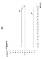
- FIG. 6 shows a case where the resistance value RL of the load circuit 26 connected to the power receiving device 3 is 1 k ⁇ , that is, when the load connected to the power receiving device 3 is small (that is, the current flowing through the load circuit 26 is small).
- FIG. 4 is a diagram showing an example of a simulation result of frequency characteristics of output voltage.
- the horizontal axis represents frequency and the vertical axis represents output voltage.
- a graph 601 represents the frequency characteristic of the output voltage when the resonance suppression coil 30 is short-circuited in the arrangement of the reception coil 21 and the resonance suppression coil 30 according to the present embodiment shown in FIG. 5A.
- the graph 602 represents the frequency characteristic of the output voltage when the resonance suppression coil 30 is short-circuited in the arrangement of the reception coil 21 and the resonance suppression coil 30 according to the comparative example shown in FIG. 5B.
- a graph 603 represents the frequency characteristic of the output voltage when the resonance suppressing coil 30 is short-circuited in the arrangement of the receiving coil 21 and the resonance suppressing coil 30 according to the comparative example shown in FIG. 5C.
- the output voltage is suppressed to be sufficiently lower than the level Th at which the overvoltage is determined.
- the output voltage is substantially equal to or higher than the level Th that is determined as the overvoltage, and it can be seen that the output voltage is not sufficiently suppressed.
- the resonance suppression coil 30 is opened, the frequency of the AC power supplied to the transmission coil 14 when the contactless power supply device performs the constant voltage output operation in both the present embodiment and the two comparative examples. Over the adjustment range, that is, the entire operating frequency range, the output voltage becomes much higher than the level Th that is determined as an overvoltage.
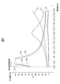
- FIG. 7 is a figure which shows an example of the simulation result of the frequency characteristic of an output voltage in case the load connected to the power receiving apparatus 3 exists.
- the horizontal axis represents frequency and the vertical axis represents output voltage.
- a graph 701 represents the frequency characteristic of the output voltage when the resonance suppression coil 30 is opened in the arrangement of the reception coil 21 and the resonance suppression coil 30 according to the present embodiment shown in FIG. 5A.
- a graph 702 represents the frequency characteristic of the output voltage when the resonance suppression coil 30 is opened in the arrangement of the reception coil 21 and the resonance suppression coil 30 according to the comparative example shown in FIG. 5B.
- a graph 703 represents the frequency characteristic of the output voltage when the resonance suppression coil 30 is opened in the arrangement of the reception coil 21 and the resonance suppression coil 30 according to the comparative example shown in FIG. 5C. Furthermore, the graph 711 represents the frequency characteristic of the output voltage when the resonance suppression coil 30 is short-circuited in the arrangement of the reception coil 21 and the resonance suppression coil 30 according to the present embodiment shown in FIG. 5A. A graph 712 represents the frequency characteristic of the output voltage when the resonance suppression coil 30 is short-circuited in the arrangement of the reception coil 21 and the resonance suppression coil 30 according to the comparative example shown in FIG. 5B.
- a graph 713 represents the frequency characteristic of the output voltage when the resonance suppression coil 30 is short-circuited in the arrangement of the reception coil 21 and the resonance suppression coil 30 according to the comparative example shown in FIG. 5C.
- the resistance value RL of the load circuit 26 was set to 10 ⁇ .
- the adjustment range of the frequency of the AC power supplied to the transmission coil 14 when the non-contact power supply device is operated to output a constant voltage, that is, the operating frequency range is 8x10 4 Hz to 9x10 4 Hz.
- the degree of coupling between the transmission coil 14 and the reception coil 21 is very high, so that the operating frequency range is The output voltage is significantly higher than the level Th at which it is determined to be an overvoltage.
- the resonance suppression coil 30 is short-circuited, the resonance condition of the resonance circuit 20 changes due to the current flowing through the resonance suppression coil 30 in both the present embodiment and the two comparative examples. The output voltage becomes sufficiently lower than the level Th at which it is determined as an overvoltage.
- the resonance occurs only when the load is connected to the power receiving device 3.
- the overvoltage protection by the suppression coil 30 fully functions.
- the coupling degree between the transmission coil 14 and the resonance suppression coil 30 is higher than the coupling degree between the transmission coil 14 and the reception coil 21 as in the present embodiment, the power receiving device 3 is connected. It can be seen that overvoltage protection works well with or without a load applied.
- the control circuit 17 of the power transmission device 2 when the control circuit 17 of the power transmission device 2 receives the abnormal voltage generation information from the communication device 15, the control circuit 17 supplies the transmission coil 14 so that the contactless power supply device 1 can perform a constant voltage output operation. The adjustment of the switching frequency and voltage of the AC power to be started is started. Then, the control circuit 17 switches the switching frequency of the AC power supplied from the power supply circuit 10 to the transmission coil 14 until the contactless power supply device 1 restarts the constant voltage output operation based on the determination information received from the communication device 15. And adjust the voltage.
- the contactless power supply device does not utilize resonance on the power transmission side, but has the same configuration as the so-called SS system. From this, the frequency characteristic of the output voltage of the non-contact power feeding apparatus 1 becomes similar to the frequency characteristic of the output voltage of the SS non-contact power feeding apparatus. Therefore, no matter which of the resistance value of the load circuit 26 and the coupling degree between the transmitting coil 14 and the receiving coil 21 changes, the switching frequency and voltage of the AC power applied to the transmitting coil 14 are appropriately adjusted to output the output. The voltage is kept almost constant.
- control circuit 17 controls the switching frequency and voltage of the AC power applied to the transmission coil 14 as described below.
- the control circuit 17 Upon receiving the abnormal voltage generation information from the communication device 15, the control circuit 17 lowers the voltage of the AC power applied to the transmission coil 14 to the lower limit voltage. As a result, on the power receiving device 3 side, even if the resonance suppression coil 30 is opened, the output voltage from the resonance circuit 20 decreases and becomes less than or equal to the upper limit threshold. Thereafter, when the determination information included in the wireless signal received from the power receiving device 3 via the communication device 15 indicates that the non-contact power feeding device 1 is not performing the constant voltage output operation, the control circuit 17 causes the AC The switching frequency of electric power is changed within a predetermined frequency range (that is, within an operating frequency range).
- the predetermined frequency range is, for example, the lower limit of the frequency at which the constant voltage output is obtained at the minimum value of the degree of coupling assumed between the transmission coil 14 and the reception coil 21 when the power transmission device 2 supplies power to the power reception device 3. Then, it is possible to set the frequency range in which the frequency at which the constant voltage output is obtained at the maximum value of the degree of coupling assumed between the transmitting coil 14 and the receiving coil 21 is the upper limit.
- the control circuit 17 may sequentially increase the switching frequency from the lower limit to the upper limit of the predetermined frequency region, or conversely, lower the switching frequency from the upper limit to the lower limit of the predetermined frequency region in order. You may.
- the control circuit 17 uses a cycle in which the determination circuit 29 switches the switching element 28 between on and off so that the determination circuit 29 of the power receiving device 3 can check whether or not the output voltage is substantially constant. It is preferable to change the switching frequency stepwise so that the same switching frequency is maintained for a long period.
- the control circuit 17 determines that the measured value of the output voltage is not included in the voltage allowable range, but the resistance of the load circuit 26 changes. However, if it is shown that the output voltage becomes substantially constant, that is, the constant voltage output operation is performed, the switching frequency is kept constant thereafter. Then, the control circuit 17 determines the relationship between the switching frequency and the duty ratio of the on/off control of the switching element SW of the power factor correction circuit 12, which produces a constant voltage output regardless of the coupling degree at the switching frequency. The duty ratio is determined by referring to the reference table shown.
- the control circuit 17 controls the gate driver 16-1 to switch ON/OFF of the switching element SW of the power factor correction circuit 12 according to the duty ratio.
- the voltage applied to the transmission coil 14 is adjusted so that the output voltage from the resonance circuit 20 is included in the voltage allowable range, that is, a constant voltage is output regardless of the coupling degree. It Then, when the determination information included in the wireless signal received from the power receiving device 3 via the communication device 15 indicates that the measured value of the output voltage is within the allowable range of the voltage, the control circuit 17 causes the transmission coil 14 to receive the measured value.
- the switching frequency and voltage of the supplied AC power are kept constant.
- control circuit 17 determines that the measured value of the output voltage is included in the determination information included in the wireless signal received from the power receiving device 3 via the communication device 15 instead of determining the duty ratio by referring to the above reference table.
- the duty ratio may be gradually changed until it is shown that the voltage is within the allowable range of the voltage.
- the power supply circuit 10 and the transmission coil 14 of the power transmission device 2 continuously perform soft switching (inductive) operation.
- the phase of the current flowing through the transmission coil 14 be delayed from the phase of the applied voltage. Accordingly, for example, when the switching element 13-1 and the switching element 13-4 are turned on, a current flows from the source terminal to the drain terminal of the switching element 13-1. The transmission coil 14 is soft-switched, and the occurrence of switching loss is suppressed.
- the power receiving device is provided with the resonance suppressing coil for changing the resonance condition of the resonance circuit.
- the reception coil and the resonance suppression coil are arranged such that the degree of coupling between the transmission coil and the resonance suppression coil of the power transmission device is higher than that of the transmission coil and the resonance suppression coil.
- the contactless power supply device changes the resonance frequency of the resonance circuit by short-circuiting the reception coil of the resonance circuit and the resonance suppression coil that can be electromagnetically coupled. Reduce the power transmitted.
- the positional relationship between the receiving coil 21 and the resonance suppression coil 30 is not limited to the above embodiment.
- FIGS. 8A and 8B are schematic cross-sectional views in a plane passing through the central axes of the reception coil 21 and the resonance suppression coil 30, showing a positional relationship between the reception coil 21 and the resonance suppression coil 30 according to a modification.
- the receiving coil 21 and the resonance suppressing coil 30 are arranged such that the receiving coil 21 is inside and the resonance suppressing coil 30 is outside with respect to the same magnetic core 21a. It is wound concentrically so that.
- the diameter of the magnetic core 14a around which the transmitting coil 14 is wound is larger than the diameter of the magnetic core 21a around which the receiving coil 21 and the resonance suppressing coil 30 are wound, and the diameter of the magnetic core 14a is equal to the diameter of the receiving coil 21. It is almost equal or more. Therefore, when the transmission coil 14, the reception coil 21, and the resonance suppression coil 30 are arranged such that the center axis of the transmission coil 14 and the center axis of the reception coil 21 are the same, the resonance suppression coil 30 is more than the reception coil 21. Is closer to the transmission coil 14. As a result, the coupling degree between the transmission coil 14 and the resonance suppression coil 30 is larger than the coupling degree between the transmission coil 14 and the reception coil 21.
- the receiving coil 21 and the resonance suppressing coil 30 have the receiving coil 21 on the outer side and the resonance suppressing coil 30 on the inner side with respect to the same magnetic core 21a. It is wound concentrically so that.
- the diameter of the magnetic core 21a around which the reception coil 21 and the resonance suppression coil 30 are wound is substantially equal to or smaller than the diameter of the resonance suppression coil 30. Therefore, when the transmission coil 14, the reception coil 21, and the resonance suppression coil 30 are arranged such that the center axis of the transmission coil 14 and the center axis of the reception coil 21 are the same, the resonance suppression coil 30 is more than the reception coil 21. Is closer to the transmission coil 14. As a result, the coupling degree between the transmission coil 14 and the resonance suppression coil 30 is larger than the coupling degree between the transmission coil 14 and the reception coil 21.
- the coupling degree between the transmission coil 14 and the resonance suppression coil 30 is larger than the coupling degree between the transmission coil 14 and the reception coil 21. Therefore, similarly to the above-described embodiment, the contactless power supply device does not connect the load circuit to the power receiving device, or even when the current flowing in the load circuit connected to the power receiving device is very small, It is possible to prevent the output voltage from rising excessively and the power receiving device or the load circuit from failing.
- the power supply circuit that supplies the AC power to the transmission coil 14 is a circuit that can variably adjust the switching frequency and the voltage applied to the transmission coil 14, It may have a circuit configuration different from that of the form.
- the power supply circuit may have a half-bridge type inverter circuit instead of the full-bridge type inverter circuit in the above embodiment.
- a capacitor (hereinafter, referred to as a series capacitor for convenience of description) that is connected in series with the transmission coil 14 may be provided in order to cut off a direct current.
- the transmission coil 14 and the series capacitor do not operate as a resonance circuit in the frequency range in which the switching frequency is adjusted. Therefore, the capacitance of the series capacitor is set so that the resonance frequency of the transmission coil 14 and the series capacitor becomes smaller than the lower limit frequency of the frequency range in which the resonance frequency and the switching frequency of the resonance circuit 20 of the power receiving device 3 are adjusted. It is preferably set.
- the contactless power feeder may be provided with a series capacitor connected in series with the transmission coil 14 in the above-described embodiment and modifications so that the contactless power supply device operates according to the so-called SS method. ..
- the resonance frequency of the transmission coil 14 and the series capacitor is set to the resonance frequency of the resonance circuit 20 of the power receiving device 3 so that the transmission coil 14 and the series capacitor operate as a resonance circuit in the frequency range in which the switching frequency is adjusted. It is preferable that the capacitance of the series capacitor is set to be substantially equal to.
- the determination circuit 29 may have a timer circuit.
- the determination circuit 29 measures the elapsed time after the resonance suppression coil 30 is short-circuited by the timer circuit, and reduces the voltage of the AC power applied to the transmission coil 14 by the control circuit 17 of the power transmission device 2.
- the switch circuit 31 may be controlled so that both ends of the resonance suppression coil 30 are opened at the time when the required predetermined period has elapsed, and on/off control of the switching element 28 may be started.
- the communication device 15 of the power transmission device 2 and the communication device 32 of the power reception device 3 may be configured to be capable of bidirectional communication.
- the control circuit 17 of the power transmission device 2 reduces the voltage of the alternating-current power applied to the transmission coil 14, the control circuit 17 notifies the communication device 32 of the power reception device 3 via the communication device 15. May be notified. Then, when the determination circuit 29 of the power receiving device 3 is notified via the communication device 32 that the voltage of the AC power applied to the transmission coil 14 has been reduced, the determination circuit 29 opens the both ends of the resonance suppression coil 30 so as to open the switch circuit. 31 may be controlled, and on/off control of the switching element 28 may be started. In this modification as well, the contactless power supply device enables continuous power transmission while preventing energy failure due to excessive increase in the output voltage from the resonance circuit and suppression of energy loss. it can.
- the switching element 28 connected between the load circuit 26 and the rectifying/smoothing circuit 23 may be omitted.
- the control circuit 17 of the power transmission device 2 receives the abnormal voltage generation information via the communication device 15, the output voltage from the resonance circuit 20 determines the voltage of the AC power applied to the transmission coil 14 as the upper threshold value. It may be lowered until it becomes less than 1.
- the power supply circuit of the power transmission device 2 can be any of various circuits capable of adjusting the voltage of the AC power applied to the transmission coil 14.
- each communication device transmits a signal including determination information and the like. It suffices to have a communication circuit capable of wired communication.
Landscapes
- Engineering & Computer Science (AREA)
- Power Engineering (AREA)
- Computer Networks & Wireless Communication (AREA)
- Signal Processing (AREA)
- Charge And Discharge Circuits For Batteries Or The Like (AREA)
Abstract
非接触給電装置1の受電装置3は、送電装置2の送信コイル14からの電力を受信する受信コイル21と、受信コイル21と直列に接続される共振コンデンサ22とを有する共振回路20を介して受電した電力を整流して得られる出力電圧の測定値が上限閾値以上となると、受信コイル21と電磁結合可能に設けられた共振抑制コイル30を短絡する。そして送信コイル14から受信コイル21へ電力が伝送されるように送電装置2と受電装置3とが配置された場合に、共振抑制コイル30と送信コイル14間の結合度が受信コイル21と送信コイル14間の結合度よりも高くなるように、受信コイル21及び共振抑制コイル30が配置される。
Description
本発明は、非接触給電装置に関する。
従来より、金属の接点などを介さずに、空間を通じて電力を伝送する、いわゆる非接触給電(ワイヤレス給電とも呼ばれる)技術が研究されている。
非接触給電技術を利用した給電装置(以下、単に非接触給電装置と呼ぶ)では、一次側(送電側)のコイル(以下、送信コイルと呼ぶ)と二次側(受電側)のコイル(以下、受信コイルと呼ぶ)とが電磁結合することにより、それら二つのコイルを介して送電側の装置から受電側の装置へ電力が伝送される。
このような非接触給電技術において、受電側の装置に、受信コイルと別個のコイルを設けることで出力電圧の過度な上昇を抑制し、あるいは、二次電流としてより大電流を得ることが提案されている(例えば、特許文献1及び2を参照)。
例えば、送信コイルと受信コイル間の位置関係が変動すると、その二つのコイル間の結合度が変化する。その結果として、受電側の装置から負荷回路への出力電圧も変動する。場合によっては、負荷回路への出力電圧が過剰に上昇して、受電側の装置または負荷回路などに故障を生じるおそれがある。そこで、特許文献1には、受電側に、受電共振コイルと磁気結合したコントロールコイルを含む共振抑制回路を設け、出力電圧を監視して、コントロールコイルをスイッチにより短絡、開放する方法で共振動作を抑制することが提案されている。
また、受電側で得られる二次電流を大電流化するために、特許文献2には、給電部が有する一次コイルに磁気結合する二次コイル及び三次コイルを有し、二次コイルに負荷に供給する電力を発生させ、三次コイルには共振用のコンデンサが接続された受電部を備える非接触電力供給装置が提案されている。この非接触電力供給装置において、二次コイルと三次コイルを別々に分離して配置し、しかも、三次コイルを二次コイルより一次コイルに近い前側に配置することが提案されている。
しかしながら、特許文献1に開示された技術では、受信コイルと接続される負荷回路が無い、あるいは、負荷回路に流れる電流が非常に小さい場合に、受電共振コイルを含む受電共振回路の共振動作を十分に抑制できず、その結果として、受電共振回路から出力される電圧の過度な上昇を抑制できないことがある。また、特許文献2に開示された技術では、共振用のコンデンサが接続された三次コイルと一次コイル間の結合度が非常に高くなった場合でも、三次コイルを含む回路の共振動作を抑制することは想定されていない。
そこで、本発明は、受電側の装置からの出力電圧が過度に上昇することを抑制できる非接触給電装置を提供することを目的とする。
本発明の一つの形態として、送電装置と、送電装置から非接触で電力伝送される受電装置とを有する非接触給電装置が提供される。この非接触給電装置において、送電装置は、受電装置へ電力を伝送する送信コイルと、送信コイルに対して、交流電力を供給する電力供給回路とを有する。また受電装置は、送電装置からの電力を受信する受信コイルと、受信コイルと直列に接続される共振コンデンサとを有する共振回路と、共振回路を介して受信した電力を整流する整流回路と、受信コイルと電磁結合可能に配置される共振抑制コイルと、共振抑制コイルと接続され、共振抑制コイルの短絡または開放を切り替え可能なスイッチ回路と、整流回路から出力される電力の出力電圧を測定して出力電圧の測定値を求める電圧検出回路と、出力電圧の測定値が所定の上限閾値以上となると、共振抑制コイルを短絡するようスイッチ回路を制御する判定回路とを有する。そして送信コイルから受信コイルへ電力が伝送されるように送電装置と受電装置とが配置された場合に、共振抑制コイルと送信コイル間の結合度が受信コイルと送信コイル間の結合度よりも高くなるように、受信コイル及び共振抑制コイルが配置される。
本発明に係る非接触給電装置は、このような構成を有することにより、受電装置からの出力電圧が過度に上昇することを抑制できる。特に、受電装置の共振回路と接続される負荷回路が無い、あるいは、その負荷回路に流れる電流が非常に小さい場合でも、出力電圧が過度に上昇することを抑制できる。
本発明に係る非接触給電装置は、このような構成を有することにより、受電装置からの出力電圧が過度に上昇することを抑制できる。特に、受電装置の共振回路と接続される負荷回路が無い、あるいは、その負荷回路に流れる電流が非常に小さい場合でも、出力電圧が過度に上昇することを抑制できる。
この非接触給電装置において、送信コイルから受信コイルへ電力が伝送されるように送電装置と受電装置とが配置された場合に、受信コイルよりも共振抑制コイルの方が送信コイルに近くなるように、受信コイル及び共振抑制コイルが配置されることが好ましい。
これにより、送信コイルから受信コイルへ電力が伝送されるように送電装置と受電装置とが配置された場合に、より確実に共振抑制コイルと送信コイル間の結合度を受信コイルと送信コイル間の結合度よりも高くすることができるので、非接触給電装置は、受電側の装置からの出力電圧が過度に上昇することをより確実に抑制できる。
これにより、送信コイルから受信コイルへ電力が伝送されるように送電装置と受電装置とが配置された場合に、より確実に共振抑制コイルと送信コイル間の結合度を受信コイルと送信コイル間の結合度よりも高くすることができるので、非接触給電装置は、受電側の装置からの出力電圧が過度に上昇することをより確実に抑制できる。
この場合において、送信コイルから受信コイルへ電力が伝送されるように送電装置と受電装置とが配置された場合に、共振抑制コイルが送信コイルと受信コイルの間に位置するように、受信コイル及び共振抑制コイルが配置されることが好ましい。
これにより、送電装置と受電装置の位置関係が、電力伝送中、あるいは、電力伝送の度に変化しても、非接触給電装置は、共振抑制コイルと送信コイル間の結合度を受信コイルと送信コイル間の結合度よりも高いまま維持することができるので、受電側の装置からの出力電圧が過度に上昇することをより確実に抑制できる。
これにより、送電装置と受電装置の位置関係が、電力伝送中、あるいは、電力伝送の度に変化しても、非接触給電装置は、共振抑制コイルと送信コイル間の結合度を受信コイルと送信コイル間の結合度よりも高いまま維持することができるので、受電側の装置からの出力電圧が過度に上昇することをより確実に抑制できる。
以下、本発明の一つの実施形態による非接触給電装置を、図を参照しつつ説明する。この非接触給電装置では、受電側の装置が、受電用の受信コイルとともに、その受信コイルと電磁結合可能なように設けられた共振抑制用のコイル(以下、単に共振抑制コイルと呼ぶ)を有する。そして受信コイルを含む共振回路からの出力電圧が所定の閾値以上となると、受電側の装置は、共振抑制コイルを短絡して共振回路の共振条件を変化させる。また、この非接触給電装置において、送電側の装置と受電側の装置間での電力伝送が可能なように送電側の装置と受電側の装置とが配置された場合、すなわち、送信コイルと受信コイルとが電磁結合するようにその二つの装置が配置された場合に、送信コイルと受信コイル間の結合度よりも送信コイルと共振抑制コイル間の結合度の方が高くなるように、共振抑制コイル及び受信コイルが配置される。これにより、この非接触給電装置は、受電側の装置と接続される負荷回路が無い、あるいは、その負荷回路に流れる電流が非常に小さい場合(例えば、負荷回路が二次電池であり、かつ、その二次電池がほぼ満充電である場合など)でも、受信コイルを含む共振回路からの出力電圧が過度に上昇することを抑制する。
図1は、本発明の一つの実施形態に係る非接触給電装置の概略構成図である。図1に示されるように、非接触給電装置1は、送電装置2と、送電装置2から空間を介して非接触で電力伝送される受電装置3とを有する。送電装置2は、電力供給回路10と、送信コイル14と、通信器15と、ゲートドライバ16-1、16-2と、制御回路17とを有する。一方、受電装置3は、受信コイル21及び共振コンデンサ22を有する共振回路20と、整流平滑回路23と、負荷回路26と、電圧検出回路27と、スイッチング素子28と、判定回路29と、共振抑制コイル30と、スイッチ回路31と、通信器32とを有する。非接触給電装置1は、送電側における共振を利用しないものの、いわゆる一次直列二次直列コンデンサ方式(以下、SS方式と呼ぶ)と同様の構成を有するため、定電圧出力動作することが可能となっている。
先ず、送電装置2について説明する。
電力供給回路10は、調節可能なスイッチング周波数、及び、調節可能な電圧を持つ交流電力を送信コイル14へ供給する。そのために、電力供給回路10は、電源11と、力率改善回路12と、4個のスイッチング素子13-1~13-4とを有する。
電力供給回路10は、調節可能なスイッチング周波数、及び、調節可能な電圧を持つ交流電力を送信コイル14へ供給する。そのために、電力供給回路10は、電源11と、力率改善回路12と、4個のスイッチング素子13-1~13-4とを有する。
電源11は、所定の脈流電圧を持つ電力を供給する。そのために、電源11は、商用の交流電源と接続され、その交流電源から供給された交流電力を整流するための全波整流回路を有する。
力率改善回路12は、電源11から出力された電力の電圧を、制御回路17からの制御に応じた電圧に変換して出力する。そのために、力率改善回路12は、例えば、電源11の正極側端子から順に直列に接続されるコイルL及びダイオードDと、コイルLとダイオードDの間にドレイン端子が接続され、電源11の負極側端子にソース端子が接続されたnチャネル型のMOSFETであるスイッチング素子SWと、ダイオードDを挟んでスイッチング素子SWと並列に接続される平滑コンデンサCを有する。またスイッチング素子SWのゲート端子は、ゲートドライバ16-1と接続される。さらに、力率改善回路12は、電源11の正極側端子と負極側端子との間に直列に接続される二つの抵抗R1、R2を有する。この抵抗R1、R2は、ダイオードDと平滑コンデンサCとの間に、平滑コンデンサCと並列に接続される。そして抵抗R1と抵抗R2間の電圧が、ダイオードDから出力される電圧を表すものとして、制御回路17により測定される。
制御回路17により指示されたデューティ比にしたがって、かつ、ダイオードDから出力される電流波形の軌跡が、電源11から供給される電圧の軌跡と一致するように、ゲートドライバ16-1がスイッチング素子SWのオン/オフを制御することにより、力率改善回路12は、力率改善動作を実行する。そしてスイッチング素子SWがオンとなるデューティ比が高くなるほど、ダイオードDから出力される電圧は高くなる。
ダイオードDから出力される電圧は、平滑コンデンサCにより平滑化されて、4個のスイッチング素子13-1~13-4を介して送信コイル14へ供給される。
なお、力率改善回路12は、上記の構成に限られず、制御回路17からの制御によって出力電圧を調整可能な他の構成を有していてもよい。
4個のスイッチング素子13-1~13-4は、フルブリッジ型のインバータ回路を構成する。そのために、スイッチング素子13-1~13-4は、例えば、nチャネル型のMOSFETとすることができる。そして4個のスイッチング素子13-1~13-4のうち、スイッチング素子13-1とスイッチング素子13-2は、電源11の正極側端子と負極側端子との間に、力率改善回路12を介して直列に接続される。また本実施形態では、電源11の正極側に、スイッチング素子13-1が接続され、一方、電源11の負極側に、スイッチング素子13-2が接続される。そしてスイッチング素子13-1のドレイン端子は、力率改善回路12を介して電源11の正極側端子と接続され、スイッチング素子13-1のソース端子は、スイッチング素子13-2のドレイン端子と接続される。また、スイッチング素子13-2のソース端子は、力率改善回路12を介して電源11の負極側端子と接続される。さらに、スイッチング素子13-1のソース端子、及び、スイッチング素子13-2のドレイン端子は、送信コイル14の一端に接続され、スイッチング素子13-2のソース端子は、スイッチング素子13-4を介して送信コイル14の他端に接続される。
同様に、4個のスイッチング素子13-1~13-4のうち、スイッチング素子13-3とスイッチング素子13-4は、スイッチング素子13-1及びスイッチング素子13-2と並列に、かつ、力率改善回路12を介して電源11の正極側端子と負極側端子との間に直列に接続される。また、電源11の正極側に、スイッチング素子13-3が接続され、一方、電源11の負極側に、スイッチング素子13-4が接続される。そしてスイッチング素子13-3のドレイン端子は、力率改善回路12を介して電源11の正極側端子と接続され、スイッチング素子13-3のソース端子は、スイッチング素子13-4のドレイン端子と接続される。また、スイッチング素子13-4のソース端子は、力率改善回路12を介して電源11の負極側端子と接続される。さらに、スイッチング素子13-3のソース端子、及び、スイッチング素子13-4のドレイン端子は、送信コイル14の他端に接続される。
また、各スイッチング素子13-1~13-4のゲート端子は、ゲートドライバ16-2を介して制御回路17と接続される。さらに、各スイッチング素子13-1~13-4のゲート端子は、オンとなる電圧が印加されたときにそのスイッチング素子がオンとなることを保証するために、それぞれ、抵抗を介して自素子のソース端子と接続されてもよい。そして各スイッチング素子13-1~13-4は、制御回路17からの制御信号にしたがって、調整可能なスイッチング周波数にてオン/オフが切り替えられる。本実施形態では、スイッチング素子13-1とスイッチング素子13-4の組と、スイッチング素子13-2とスイッチング素子13-3との組について交互にオン/オフが切り替えられる。すなわち、スイッチング素子13-1とスイッチング素子13-4とがオンとなっている間、スイッチング素子13-2とスイッチング素子13-3とがオフとなる。逆に、スイッチング素子13-2とスイッチング素子13-3とがオンとなっている間、スイッチング素子13-1とスイッチング素子13-4とがオフとなる。これにより、電源11から力率改善回路12を介して供給された直流電力は、各スイッチング素子のスイッチング周波数を持つ交流電力に変換されて、送信コイル14に供給される。
そして送信コイル14は、電力供給回路10から供給された交流電力を、空間を介して受電装置3の共振回路20へ伝送する。
通信器15は、受電装置3の通信器32から無線信号を受信する度に、その無線信号から、受電装置3の整流平滑回路23からの出力電圧が過度に上昇したことを表す異常電圧発生情報、または、非接触給電装置1が定電圧出力動作しているか否かなどを表す判定情報を取り出して、制御回路17へ出力する。そのために、通信器15は、例えば、所定の無線通信規格に準じて無線信号を受信するアンテナと、その無線信号を復調する通信回路とを有する。なお、所定の無線通信規格は、例えば、ISO/IEC 15693、ZigBee(登録商標)、あるいはBluetooth(登録商標)とすることができる。
ゲートドライバ16-1は、制御回路17から、力率改善回路12のスイッチング素子SWのオン/オフを切り替える制御信号を受信し、その制御信号に応じて、スイッチング素子SWのゲート端子に印加する電圧を変化させる。すなわち、ゲートドライバ16-1は、スイッチング素子SWをオンにする制御信号を受け取ると、スイッチング素子SWのゲート端子に、スイッチング素子SWがオンとなる相対的に高い電圧を印加する。一方、ゲートドライバ16-1は、スイッチング素子SWをオフにする制御信号を受け取ると、スイッチング素子SWのゲート端子に、スイッチング素子SWがオフとなる、相対的に低い電圧を印加する。これにより、ゲートドライバ16-1は、制御回路17により指示されたタイミングで力率改善回路12のスイッチング素子SWのオン/オフを切り替える。
ゲートドライバ16-2は、制御回路17から、各スイッチング素子13-1~13-4のオン/オフを切り替える制御信号を受信し、その制御信号に応じて、各スイッチング素子13-1~13-4のゲート端子に印加する電圧を変化させる。すなわち、ゲートドライバ16-2は、スイッチング素子13-1及びスイッチング素子13-4をオンにする制御信号を受け取ると、スイッチング素子13-1のゲート端子及びスイッチング素子13-4のゲート端子に、スイッチング素子13-1及びスイッチング素子13-4がオンとなる相対的に高い電圧を印加する。これにより、電源11からの電流が、スイッチング素子13-1、送信コイル14及びスイッチング素子13-4を介して流れるようになる。一方、ゲートドライバ16-2は、スイッチング素子13-1及びスイッチング素子13-4をオフにする制御信号を受け取ると、スイッチング素子13-1のゲート端子及びスイッチング素子13-4のゲート端子に、スイッチング素子13-1及びスイッチング素子13-4がオフとなる相対的に低い電圧を印加する。これにより、電源11からの電流がスイッチング素子13-1及びスイッチング素子13-4を流れなくなる。ゲートドライバ16-2は、スイッチング素子13-2及びスイッチング素子13-3についても同様に、ゲート端子に印加する電圧を制御する。したがって、スイッチング素子13-1及びスイッチング素子13-4がオフとなり、スイッチング素子13-2及びスイッチング素子13-3がオンとなると、電源11からの電流が、スイッチング素子13-3、送信コイル14及びスイッチング素子13-2を介して流れるようになる。
制御回路17は、例えば、不揮発性のメモリ回路及び揮発性のメモリ回路と、演算回路と、他の回路と接続するためのインターフェース回路とを有する。そして制御回路17は、通信器15から異常電圧発生情報を受け取ると、電力供給回路10から送信コイル14に供給される交流電力のスイッチング周波数及び電圧の制御を開始する。その後、制御回路17は、通信器15から判定情報を受け取る度に、その判定情報に応じて、電力供給回路10から送信コイル14に供給される交流電力のスイッチング周波数及び電圧を制御する。
そのために、本実施形態では、制御回路17は、各スイッチング素子13-1~13-4を制御する。具体的に、制御回路17は、スイッチング素子13-1及びスイッチング素子13-4の組とスイッチング素子13-2及びスイッチング素子13-3の組とを交互にオンにする。さらに、制御回路17は、スイッチング周波数に対応する1周期内でスイッチング素子13-1及びスイッチング素子13-4の組がオンとなっている期間とスイッチング素子13-2及びスイッチング素子13-3の組がオンとなっている期間とを等しくする。なお、制御回路17は、スイッチング素子13-1及びスイッチング素子13-4の組とスイッチング素子13-2及びスイッチング素子13-3の組が同時にオンとなり、電源11が短絡されることを防止することが好ましい。そのために、制御回路17がスイッチング素子13-1及びスイッチング素子13-4の組とスイッチング素子13-2及びスイッチング素子13-3の組のオン/オフを切り替える際に、両方のスイッチング素子の組がオフとなるデッドタイムを設けてもよい。
また、制御回路17は、スイッチング周波数と、そのスイッチング周波数にて定電圧出力となる、送信コイル14への印加電圧に相当する、力率改善回路12のスイッチング素子SWのオン/オフ制御のデューティ比との関係を表す参照テーブルを参照して、スイッチング周波数に応じたデューティ比を選択する。そして制御回路17は、そのデューティ比と、力率改善回路12のダイオードDからの出力電圧の変化に応じて、スイッチング素子SWのオン/オフを切り替えるタイミングを決定し、そのタイミングを表す制御信号をゲートドライバ16-1へ出力する。
さらに、通信器15が受電装置3からの無線信号を受信できない場合、受電装置3は、送電装置2から電力供給を受けることができる位置に存在しない、すなわち、送電装置2は待機状態にあると想定される。そこでこの場合、制御回路17は、スイッチング素子SWのオン/オフ制御のデューティ比を設定可能な最小値としてもよい。これにより、送電装置2が待機状態となっている間、送信コイル14に印加される電圧も設定可能な最小値となるので、エネルギーの損失が抑制される。
なお、制御回路17による、スイッチング周波数及び送信コイル14への印加電圧の制御の詳細については後述する。
次に、受電装置3について説明する。
共振回路20は、互いに直列に接続される受信コイル21と共振コンデンサ22とからなるLC共振回路である。そして共振回路20が有する受信コイル21の一端が共振コンデンサ22を介して整流平滑回路23の一方の入力端子に接続される。また、受信コイル21の他端が、整流平滑回路23の他方の入力端子に接続される。
共振回路20は、互いに直列に接続される受信コイル21と共振コンデンサ22とからなるLC共振回路である。そして共振回路20が有する受信コイル21の一端が共振コンデンサ22を介して整流平滑回路23の一方の入力端子に接続される。また、受信コイル21の他端が、整流平滑回路23の他方の入力端子に接続される。
受信コイル21は、共振コンデンサ22とともに、送電装置2の送信コイル14に流れる交流電流と共振することで、送信コイル14から電力を受信する。そして受信コイル21は、共振コンデンサ22を介して、受信した電力を整流平滑回路23へ出力する。なお、受信コイル21の巻き数と、送電装置2の送信コイル14の巻き数は同一でもよく、あるいは、異なっていてもよい。
共振コンデンサ22は、受信コイル21と直列に接続される。すなわち、共振コンデンサ22は、その一端で受信コイル21の一端と接続され、他端で整流平滑回路23と接続される。そして共振コンデンサ22は、受信コイル21とともに共振することで受信した電力を整流平滑回路23へ出力する。
整流平滑回路23は、整流回路の一例であり、ブリッジ接続された4個のダイオードを有する全波整流回路24と平滑コンデンサ25とを有し、共振回路20により受信され、かつ、共振回路20から受け取った電力を整流し、かつ、平滑化して、直流電力に変換する。そして整流平滑回路23は、その直流電力を、負荷回路26に出力する。
電圧検出回路27は、整流平滑回路23の両端子間の出力電圧を所定の周期ごとに測定する。整流平滑回路23の両端子間の出力電圧は、共振回路20の出力電圧と1対1に対応するので、整流平滑回路23の両端子間の出力電圧の測定値は、間接的に共振回路20の出力電圧の測定値となる。電圧検出回路27は、例えば、直流電圧を検出できる公知の様々な電圧検出回路の何れかとすることができる。そして電圧検出回路27は、その出力電圧の測定値を表す電圧検出信号を判定回路29へ出力する。
スイッチング素子28は、例えば、MOSFETであり、整流平滑回路23と負荷回路26との間に接続される。スイッチング素子28は、オフとなると整流平滑回路23から負荷回路26へ電流が流れないようにし、一方、オンとなると整流平滑回路23から負荷回路26へ電流が流れるようにする。
判定回路29は、電圧検出回路27から受け取った出力電圧の測定値が所定の上限閾値以上となっているか否か判定する。そしてその測定値が上限閾値以上となっている場合、共振抑制コイル30を短絡するよう、スイッチ回路31を制御するとともに、出力電圧の測定値が上限閾値以上となったこと、すなわち、出力電圧が過度に上昇したことを通信器32へ通知する。これにより、判定回路29は、出力電圧の測定値が上限閾値に達すると直ちに共振回路20の共振周波数を変更して送電装置2と受電装置3間で伝送される電力を低下させ、その結果として共振回路20からの出力電圧を低下させることができる。なお、上限閾値は、負荷回路26及び受電装置3が故障しない電圧の上限値またはその上限値から所定のオフセット値を減じた値とすることができる。
さらに、判定回路29は、送信コイル14に印加される交流電力のスイッチング周波数及び電圧が制御されている間、出力電圧の測定値が、定電圧出力動作が行われているときの電圧の許容範囲内に出力電圧の測定値が含まれているか否か判定する。そして判定回路29は、その判定結果を通信器32へ通知する。なお、電圧の許容範囲の上限は、上記の上限閾値以下に設定されることが好ましい。
そのために、判定回路29は、例えば、電圧の許容範囲を記憶するメモリ回路と、出力電圧の測定値を、上限閾値及び電圧の許容範囲のそれぞれと比較する演算回路と、スイッチング素子28及びスイッチ回路31のオン/オフを制御するための制御回路を有する。なお、判定回路29は、出力電圧の測定値を上限閾値と比較し、その結果に応じてスイッチ回路31のオン/オフを切り替えるための回路として、特許文献1に記載のコントロールコイルのオン/オフの制御に用いられる回路と同様の回路を有していてもよい。この場合、スイッチ回路31をオンにする電圧よりも、スイッチ回路31をオフにする電圧は低く設定されてもよい。
さらに、判定回路29は、出力電圧の測定値が、電圧の許容範囲から外れている間、所定の周期でスイッチング素子28のオン/オフを切り替える。これにより、その所定の周期で、整流平滑回路23と接続される、負荷回路26を含む回路全体の抵抗値が変化する。したがって、判定回路29は、スイッチング素子28のオン/オフを切り替えながら、出力電圧の測定値が略一定となるか否かを判定することで、非接触給電装置1が定電圧出力動作しているか否かを判定できる。そこで、判定回路29は、所定の周期でスイッチング素子28のオン/オフを切り替えても出力電圧の測定値が略一定となっている間、非接触給電装置1が定電圧出力動作していることを通信器32へ通知する。
また、判定回路29は、出力電圧の測定値が所定の周期よりも長い一定期間の間、非接触給電装置1が定電圧出力動作している場合、スイッチング素子28のオン/オフの切り替えを停止して、オンとなる状態を維持する。そして判定回路29は、出力電圧の測定値が電圧の許容範囲に含まれるか否か判定し、その判定結果を通信器32へ通知する。
その際、判定回路29は、出力電圧の測定値が所定の周期よりも長い一定期間の間、電圧の許容範囲に含まれる場合、非接触給電装置1が定電圧出力動作しており、かつ、出力電圧の測定値が電圧の許容範囲内であることを表す判定結果を通信器32へ通知する。
なお、変形例によれば、判定回路29は、整流平滑回路23に対して、負荷回路26と並列に接続される抵抗を有していてもよい。この場合、スイッチング素子28は、その抵抗と直列、かつ、負荷回路26と並列となるように設けられてもよい。この場合には、出力電圧の測定値が電圧の許容範囲に含まれる間、判定回路29は、スイッチング素子28をオフにする。一方、出力電圧の測定値が電圧の許容範囲から外れると、上記の実施形態と同様に、判定回路29は、所定の周期でスイッチング素子28のオン/オフを切り替えればよい。この変形例によれば、非接触給電装置1が定電圧出力動作していない場合にも、負荷回路26への電力供給が継続される。
さらに他の変形例によれば、上記の抵抗と並列、かつ、負荷回路26と直列に、MOSFETといった第2のスイッチング素子が設けられてもよい。この場合、出力電圧の測定値が電圧の許容範囲に含まれる間、判定回路29は、第2のスイッチング素子をオンにして、負荷回路26への電力供給を可能とする。一方、出力電圧の測定値が電圧の許容範囲から外れると、判定回路29は、第2のスイッチング素子をオフにして、負荷回路26への電力供給を停止してもよい。これにより、送電装置2においてスイッチング周波数が調整されている間に、受電した電力の電圧が過度に高くなっても、その過度に高い電圧が負荷回路26に印加されることが防止される。
共振抑制コイル30は、共振回路20の受信コイル21と電磁結合可能に設けられる。例えば、共振抑制コイル30と受信コイル21とは、同一の磁心に対して巻き付けられる。また共振抑制コイル30の両端は、それぞれ、スイッチ回路31と接続される。そして共振抑制コイル30がスイッチ回路31により短絡されると、共振抑制コイル30は受信コイル21と電磁結合し、共振回路20の共振周波数が変化する。そのため、共振回路20からの出力電圧が過度に上昇しても、共振抑制コイル30が短絡されることで、送電装置2から受電装置3へ伝送される電力が低下するので、共振回路20からの出力電圧も低下する。なお、受信コイル21の巻き数と共振抑制コイル30の巻き数は等しくてもよく、あるいは、異なっていてもよい。さらに、送信コイル14の巻き数と共振抑制コイル30の巻き数は等しくてもよく、あるいは、異なっていてもよい。
一方、スイッチ回路31が共振抑制コイル30の両端を開放すると、共振抑制コイル30は、送信コイル14と受信コイル21間の共振に関与しなくなり、送電装置2から受電装置3への電力伝送に影響しなくなる。
また、共振抑制コイル30は、送信コイル14と受信コイル21とが電磁結合する際に、送信コイル14と受信コイル21間の結合度よりも送信コイル14と共振抑制コイル30間の結合度の方が高くなるように配置される。なお、送信コイル14、受信コイル21及び共振抑制コイル30の位置関係の詳細については後述する。
スイッチ回路31は、共振抑制コイル30の両端と接続され、判定回路29からの制御信号に応じて共振抑制コイル30を短絡するか、開放するかを切り替える。すなわち、スイッチ回路31は、判定回路29からオンとなる制御信号を受信している間、共振抑制コイル30を短絡する。一方、スイッチ回路31は、判定回路29からオフとなる制御信号を受信している間、共振抑制コイル30の両端を開放する。
図2A~図2Dは、それぞれ、スイッチ回路31の一例を示す図である。図2Aに示される例では、スイッチ回路31はリレーを有する。判定回路29がリレーをオンにすると共振抑制コイル30が短絡される。一方、判定回路29がリレーをオフにすると共振抑制コイル30の両端が開放される。
図2Bに示される例では、スイッチ回路31は、共振抑制コイル30の両端間に直列に接続される、二つのnチャネル型のMOSFETを有する。そして二つのMOSFETは、互いのソース端子同士が接続され、ドレイン端子が共振抑制コイル30の両端のそれぞれと接続されるように配置される。また二つのMOSFETのゲート端子は判定回路29と接続される。そして判定回路29から、オンとなる制御信号に相当する、相対的に高い電圧が二つのMOSFETのゲート端子に印加されると、各MOSFETのソース-ドレイン間を電流が流れることが可能となるので、共振抑制コイル30は短絡される。一方、判定回路29から、オフとなる制御信号に相当する、相対的に低い電圧が二つのMOSFETのゲート端子に印加されると、各MOSFETのソース-ドレイン間を電流が流れなくなり、かつ、二つのMOSFETのボディダイオードも互いに逆向きとなっているため、それぞれのボディダイオードを通じても電流は流れない。そのため、共振抑制コイル30の両端は開放される。
図2Cに示される例でも、図2Bに示される例と同様に、スイッチ回路31は、共振抑制コイル30の両端間に直列に接続される、二つのnチャネル型のMOSFETを有する。ただし、図2Cに示される例では、二つのMOSFETは、互いのドレイン端子同士が接続され、ソース端子が共振抑制コイル30の両端のそれぞれと接続されるように配置される。この例でも、判定回路29から、オンとなる制御信号に相当する、相対的に高い電圧が二つのMOSFETのゲート端子に印加されると、共振抑制コイル30は短絡される。一方、判定回路29から、オフとなる制御信号に相当する、相対的に低い電圧が二つのMOSFETのゲート端子に印加されると、共振抑制コイル30の両端は開放される。
図2Dに示される例では、スイッチ回路31は、共振抑制コイル30の両端間に直列に接続される、nチャネル型のMOSFETとダイオードとを有する。MOSFETのドレイン端子は共振抑制コイル30の一端と接続され、ソース端子は、ダイオードのアノード端子と接続される。そしてMOSFETのゲート端子は判定回路29と接続される。またダイオードのカソード端子は共振抑制コイル30の他端と接続される。この例でも、判定回路29から、オンとなる制御信号に相当する電圧がMOSFETのゲート端子に印加されると、共振抑制コイル30は短絡される。一方、判定回路29から、オフとなる制御信号に相当する電圧がMOSFETのゲート端子に印加されると、共振抑制コイル30の両端は開放される。なお、この例では、MOSFETがオンとなっても、ダイオードからMOSFET側へ流れる電流は遮断されるので、共振抑制コイル30を流れる交流電流の周期のうちの1/2の期間では、共振抑制コイル30は、共振回路20の共振に影響しない。しかしこの場合でも、送電装置2から受電装置3へ伝送される電力は低下するので、共振回路20からの出力電圧は低下する。
通信器32は、判定回路29から、出力電圧の測定値が上限閾値以上となったことを通知されると、その通知内容を表す異常電圧発生情報を含む無線信号(出力電圧異常信号)を生成し、その無線信号を送電装置2の通信器15へ向けて送信する。また通信器32は、出力電圧の測定値が上限閾値以上となってから、定電圧出力動作が再開されるまで、所定の送信周期ごとに、判定回路29から受け取った判定結果に応じて、非接触給電装置1が定電圧出力動作しているか否か、及び、出力電圧の測定値が電圧の許容範囲に含まれるか否かを表す判定情報を含む無線信号を生成する。そして通信器32は、その無線信号を送電装置2の通信器15へ向けて送信する。そのために、通信器32は、例えば、所定の無線通信規格に準じて無線信号を生成する通信回路と、その無線信号を出力するアンテナとを有する。なお、所定の無線通信規格は、通信器15と同様に、例えば、ISO/IEC 15693、ZigBee(登録商標)、あるいはBluetooth(登録商標)とすることができる。
以下、送信コイル14、受信コイル21及び共振抑制コイル30の位置関係の詳細について説明する。
図3Aは、送信コイル14、受信コイル21及び共振抑制コイル30の位置関係の一例を示す、送信コイル14、受信コイル21及び共振抑制コイル30の中心軸を通る平面における概略断面図である。図3Bは、送信コイル14側から見た受信コイル21及び共振抑制コイル30の配置の一例の概略平面図である。
図3A及び図3Bに示される例では、送信コイル14は、ポットコアの磁心14aに巻き付けられる。同様に、受信コイル21及び共振抑制コイル30は、同一のポットコアの磁心21aに巻き付けられる。そして送電装置2から受電装置3へ電力伝送可能なように送電装置2と受電装置3とが配置された場合において、送信コイル14側から見て、手前側に共振抑制コイル30が位置し、奥側に受信コイル21が位置するように、すなわち、共振抑制コイル30が送信コイル14と受信コイル21との間に位置するように、受信コイル21及び共振抑制コイル30は配置される。これにより、送電装置2から受電装置3へ電力伝送可能なように送電装置2と受電装置3とが配置された場合、共振抑制コイル30の方が受信コイル21よりも送信コイル14に近くなるので、共振抑制コイル30と送信コイル14間の結合度が受信コイル21と送信コイル14間の結合度よりも高くなる。したがって、共振抑制コイル30が短絡されると、送信コイル14に印加される電力に応じて共振抑制コイル30にある程度の電流が流れ、その電流により生じる磁界により、受信コイル21を含む共振回路20の共振条件が変動するため、共振回路20からの出力電力が過度に上昇することが抑制される。また、上記のように受信コイル21と共振抑制コイル30とが配置されることにより、送電装置2と受電装置3の位置関係が、電力伝送中、あるいは、電力伝送の度に変化しても、共振抑制コイル30と送信コイル14間の結合度が受信コイル21と送信コイル14間の結合度よりも高いまま維持される。
図4A~図4Cは、受信コイル21及び共振抑制コイル30の位置関係の他の一例を示す、受信コイル21及び共振抑制コイル30の中心軸を通る平面における概略断面図である。図4Dは、送信コイル14側から見た受信コイル21及び共振抑制コイル30の配置の他の一例の概略平面図である。
図4A~図4Cの何れに示される例でも、受信コイル21及び共振抑制コイル30は、同一のコアに巻き付けられる。ただし、図4Aに示される例では、コア21bは磁心を有さないタイプのコアである。また、図4Bに示される例では、コア21cは、受信コイル21及び共振抑制コイル30を覆うカバーを有さない、凸型コアである。さらに、図4Cに示される例では、コア21dは、平板状のコアである。
また、図4Dに示されるように、受信コイル21及び共振抑制コイル30は、外形が略矩形のコア21eに巻き付けられてもよい。なお、コア21eは、ポットコアでもよく、あるいは、凸型コアまたは平板状のコアでもよい。
さらに、図4A~図4Dに示される何れの例についても、図3A及び図3Bに示される例と同様に、送電装置2から受電装置3へ電力伝送可能なように送電装置2と受電装置3とが配置された場合において、共振抑制コイル30の方が受信コイル21よりも送信コイル14に近くなる。すなわち、送信コイル14側から見て、手前側に共振抑制コイル30が位置し、奥側に受信コイル21が位置するように、受信コイル21及び共振抑制コイル30は配置される。したがって、これらの例でも、送電装置2から受電装置3へ電力伝送可能なように送電装置2と受電装置3とが配置された場合、送信コイル14と共振抑制コイル30間の結合度が送信コイル14と受信コイル21間の結合度よりも高くなる。
次に、送信コイル14、受信コイル21及び共振抑制コイル30間のそれぞれの結合度の大小関係を変化させたときの共振回路20からの出力電圧の周波数特性のシミュレーション結果について説明する。
図5Aは、本実施形態による、送信コイル14、受信コイル21及び共振抑制コイル30の中心軸を通る平面における概略断面図である。図5B及び図5Cは、比較例による、送信コイル14、受信コイル21及び共振抑制コイル30の中心軸を通る平面における概略断面図である。なお、図5A~図5Cでは、簡単化のために、各コイルの断面のうち、中心軸を一方の端とする半分が図示される。
図5Aに示されるように、本実施形態では、送電装置2から受電装置3へ電力伝送可能なように送電装置2と受電装置3とが配置された場合において、共振抑制コイル30の方が受信コイル21よりも送信コイル14に近くなるように、受信コイル21及び共振抑制コイル30は配置される。一方、図5Bに示される比較例では、送電装置2から受電装置3へ電力伝送可能なように送電装置2と受電装置3とが配置された場合において、受信コイル21の方が共振抑制コイル30よりも送信コイル14に近くなるように、受信コイル21及び共振抑制コイル30は配置される。また、図5Cに示される例では、受信コイル21と共振抑制コイル30とは、同じ磁心に対して、受信コイル21が内側となり、共振抑制コイル30が外側となるように同心円状に巻き付けられる。
このシミュレーションにおいて、送信コイル14に流れる電流I1、受信コイル21に流れる電流I2、共振抑制コイル30に流れる電流I3と、送信コイル14に印加される交流電力の電圧V1との関係は次式で表されるものとした。

ここで、k12は、送信コイル14と受信コイル21間の結合度であり、k13は、送信コイル14と共振抑制コイル30間の結合度であり、k23は、受信コイル21と共振抑制コイル30間の結合度である。また、L1、L2、L3は、それぞれ、送信コイル14、受信コイル21、及び共振抑制コイル30のインダクタンスである。さらに、C1は、送信コイル14と直列接続されるコンデンサの静電容量であり、R1は、送電側の巻線抵抗値である。なお、本実施形態では、送信コイル14と直列接続されるコンデンサは存在しないので、送信コイル14とコンデンサとにより構成される共振回路の共振周波数が、送信コイル14に印加される交流電力の周波数の調整範囲よりも低い値となるように、C1=1650nFとした。さらにまた、R2は、受電側の巻き線抵抗値であり、R3は、共振抑制コイル30の巻き線抵抗値である。そしてC2は、共振コンデンサ22の静電容量であり、RLは、負荷回路26の抵抗値であり、Rdsは、共振抑制コイル30が短絡された場合における、共振抑制コイル30を含む閉回路の抵抗値である。また、ωは、送信コイル14に印加される交流電力の角周波数であり、その交流電力の周波数fを用いてω=2πfで表される。なお、共振回路20からの出力電圧V2は、電流I2及び抵抗値RLに基づいて算出される(すなわち、V2=RL*I2)。また、このシミュレーションでは、送信コイル14のインダクタンスL1及び受信コイル21のインダクタンスL2を250μHとし、共振抑制コイル30のインダクタンスL3を15μHとした。また、共振コンデンサ22の静電容量C2を16.5nFとし、送電側の巻線抵抗値R1、受電側の巻線抵抗値R2を0.1Ωとし、共振抑制コイル30を含む回路の抵抗値(R3+Rds)を0.035Ωとした。さらに、送信コイル14に印加される交流電力の電圧V1を330Vとした。
図5Aに示される実施形態及び図5B及び図5Cに示される各比較例において、送信コイル14が巻き付けられるコアの磁心の直径及び透磁率と、受信コイル21及び共振抑制コイル30が巻き付けられるコアの磁心の直径及び透磁率とは同一であるとした。また、図5Aに示される実施形態及び図5B及び図5Cに示される各比較例において、送信コイル14、受信コイル21及び共振抑制コイル30は同軸状に配置されるものとし、受信コイル21及び共振抑制コイル30のうちの送信コイル14側に配置されるものと送信コイル14との距離は等しいとした。
図5Aに示される本実施形態では、送信コイル14と受信コイル21間の結合度K12よりも、送信コイル14と共振抑制コイル30間の結合度K13の方が大きくなる。このシミュレーションでは、送信コイル14と受信コイル21間の結合度K12は0.504であり、送信コイル14と共振抑制コイル30間の結合度K13は0.583であり、受信コイル21と共振抑制コイル30間の結合度K23は0.882であった。また、図5Bに示される比較例では、送信コイル14と受信コイル21間の結合度K12よりも、送信コイル14と共振抑制コイル30間の結合度K13の方が小さくなる。そのため、このシミュレーションでは、送信コイル14と受信コイル21間の結合度K12は0.532であり、送信コイル14と共振抑制コイル30間の結合度K13は0.440であり、受信コイル21と共振抑制コイル30間の結合度K23は0.914であった。さらに、図5Cに示される比較例では、送信コイル14に対して受信コイル21の対向する面の方が、送信コイル14に対して共振抑制コイル30の対向する面よりも広いため、送信コイル14と受信コイル21間の結合度K12よりも、送信コイル14と共振抑制コイル30間の結合度K13の方が小さくなる。そのため、このシミュレーションでは、送信コイル14と受信コイル21間の結合度K12は0.520であり、送信コイル14と共振抑制コイル30間の結合度K13は0.466であり、受信コイル21と共振抑制コイル30間の結合度K23は0.846であった。
図6は、受電装置3に接続される負荷回路26の抵抗値RLが1kΩである場合、すなわち、受電装置3に接続される負荷が小さい(すなわち、負荷回路26に流れる電流が小さい)場合における、出力電圧の周波数特性のシミュレーション結果の一例を示す図である。図6において、横軸は、周波数を表し、縦軸は、出力電圧を表す。グラフ601は、図5Aに示される本実施形態による、受信コイル21と共振抑制コイル30の配置における、共振抑制コイル30が短絡されたときの出力電圧の周波数特性を表す。グラフ602は、図5Bに示される比較例による、受信コイル21と共振抑制コイル30の配置における、共振抑制コイル30が短絡されたときの出力電圧の周波数特性を表す。また、グラフ603は、図5Cに示される比較例による、受信コイル21と共振抑制コイル30の配置における、共振抑制コイル30が短絡されたときの出力電圧の周波数特性を表す。グラフ601に示されるように、本実施形態によれば、負荷回路26の抵抗値Roが1kΩであっても、出力電圧は過電圧と判定されるレベルThよりも十分に低く抑制される。一方、グラフ602及びグラフ603に示されるように、比較例では、出力電圧は過電圧と判定されるレベルThと略等しいかそれ以上となっており、出力電圧の抑制が十分でないことが分かる。なお、共振抑制コイル30が開放される場合には、本実施形態及び二つの比較例の何れについても、非接触給電装置を定電圧出力動作させる際に送信コイル14に供給される交流電力の周波数の調整範囲、すなわち動作周波数の範囲全体にわたって出力電圧は過電圧と判定されるレベルThよりも遥かに高くなる。
図7は、受電装置3に接続される負荷が有る場合における、出力電圧の周波数特性のシミュレーション結果の一例を示す図である。図7において、横軸は、周波数を表し、縦軸は、出力電圧を表す。グラフ701は、図5Aに示される本実施形態による、受信コイル21と共振抑制コイル30の配置における、共振抑制コイル30が開放されたときの出力電圧の周波数特性を表す。グラフ702は、図5Bに示される比較例による、受信コイル21と共振抑制コイル30の配置における、共振抑制コイル30が開放されたときの出力電圧の周波数特性を表す。また、グラフ703は、図5Cに示される比較例による、受信コイル21と共振抑制コイル30の配置における、共振抑制コイル30が開放されたときの出力電圧の周波数特性を表す。さらに、グラフ711は、図5Aに示される本実施形態による、受信コイル21と共振抑制コイル30の配置における、共振抑制コイル30が短絡されたときの出力電圧の周波数特性を表す。グラフ712は、図5Bに示される比較例による、受信コイル21と共振抑制コイル30の配置における、共振抑制コイル30が短絡されたときの出力電圧の周波数特性を表す。そしてグラフ713は、図5Cに示される比較例による、受信コイル21と共振抑制コイル30の配置における、共振抑制コイル30が短絡されたときの出力電圧の周波数特性を表す。なお、このシミュレーションでは、負荷回路26の抵抗値RLを10Ωとした。また、非接触給電装置を定電圧出力動作させる際に送信コイル14に供給される交流電力の周波数の調整範囲、すなわち動作周波数の範囲は、8x104Hz~9x104Hzの範囲であるとした。
このシミュレーションでは、受信コイル21と共振抑制コイル30の位置関係によらず、共振抑制コイル30が開放されているときには、送信コイル14と受信コイル21間の結合度が非常に高いため、動作周波数範囲内で出力電圧が過電圧と判定されるレベルThよりも著しく高くなっている。一方、共振抑制コイル30が短絡されると、本実施形態及び二つの比較例の何れについても、共振抑制コイル30に流れる電流により共振回路20の共振条件が変化するので、動作周波数範囲内では、出力電圧が過電圧と判定されるレベルThよりも十分に低くなる。
このように、送信コイル14と受信コイル21間の結合度が送信コイル14と共振抑制コイル30間の結合度よりも高い場合には、受電装置3に負荷が接続されているときに限り、共振抑制コイル30による過電圧保護が十分に機能する。これに対して、本実施形態のように、送信コイル14と受信コイル21間の結合度よりも送信コイル14と共振抑制コイル30間の結合度の方が高い場合には、受電装置3に接続される負荷の有無にかかわらず、過電圧保護が十分に機能することが分かる。
以下、非接触給電装置1の動作の詳細について説明する。
本実施形態では、送電装置2の制御回路17は、通信器15から異常電圧発生情報を受け取ると、非接触給電装置1が定電圧出力動作することが可能となるように、送信コイル14に供給される交流電力のスイッチング周波数及び電圧の調整を開始する。そして制御回路17は、通信器15から受け取った判定情報に基づいて、非接触給電装置1が定電圧出力動作を再開するまで、電力供給回路10から送信コイル14に供給される交流電力のスイッチング周波数及び電圧を調整する。
上述したように、本実施形態による非接触給電装置は、送電側における共振を利用しないものの、いわゆるSS方式と同様の構成を有する。このことから、非接触給電装置1の出力電圧の周波数特性は、SS方式の非接触給電装置の出力電圧の周波数特性と類似したものとなる。したがって、負荷回路26の抵抗値及び送信コイル14と受信コイル21間の結合度の何れが変動しても、送信コイル14に印加する交流電力のスイッチング周波数及び電圧を適切に調節することで、出力電圧が略一定に保たれる。
そこで、制御回路17は、定電圧出力動作を達成するために、下記のように送信コイル14に印加される交流電力のスイッチング周波数及び電圧を制御する。
通信器15から異常電圧発生情報を受け取ると、制御回路17は、送信コイル14に印加される交流電力の電圧を下限の電圧まで低下させる。これにより、受電装置3側では、共振抑制コイル30が開放されても、共振回路20からの出力電圧が低下し、上限閾値以下となる。その後、受電装置3から通信器15を介して受けとった無線信号に含まれる判定情報において、非接触給電装置1が定電圧出力動作していないことが示されている場合、制御回路17は、交流電力のスイッチング周波数を所定の周波数領域内(すなわち、動作周波数範囲内)で変化させる。所定の周波数領域は、例えば、送電装置2から受電装置3への給電が行われる場合における、送信コイル14と受信コイル21間の想定される結合度の最小値において定電圧出力となる周波数を下限とし、送信コイル14と受信コイル21間の想定される結合度の最大値において定電圧出力となる周波数を上限とする周波数領域とすることができる。
制御回路17は、スイッチング周波数を変化させる際、所定の周波数領域の下限から上限まで順にスイッチング周波数を高くしてもよく、あるいは、逆に、所定の周波数領域の上限から下限まで順にスイッチング周波数を低くしてもよい。その際、制御回路17は、受電装置3の判定回路29が、出力電圧が略一定となったか否かを調べることができるように、判定回路29がスイッチング素子28のオンとオフを切り替える周期よりも長い期間、同じスイッチング周波数を保つように、ステップ状にスイッチング周波数を変化させることが好ましい。
制御回路17は、受電装置3から通信器15を介して受けとった無線信号に含まれる判定情報において、出力電圧の測定値が電圧の許容範囲には含まれないものの、負荷回路26の抵抗が変化しても略一定となること、すなわち、定電圧出力動作が行われていることが示されていると、それ以降、スイッチング周波数を一定に保つ。そして次に、制御回路17は、スイッチング周波数と、そのスイッチング周波数において結合度によらず一定の電圧出力となる、力率改善回路12のスイッチング素子SWのオン/オフ制御のデューティ比との関係を示す参照テーブルを参照して、そのデューティ比を決定する。そして制御回路17は、そのデューティ比に従って力率改善回路12のスイッチング素子SWのオン/オフを切り替えるよう、ゲートドライバ16-1を制御する。これにより、共振回路20からの出力電圧が電圧の許容範囲に含まれるように、すなわち、結合度によらずに一定の電圧が出力されるように、送信コイル14に印加される電圧が調整される。そして制御回路17は、受電装置3から通信器15を介して受けとった無線信号に含まれる判定情報において、出力電圧の測定値が電圧の許容範囲に含まれることが示されると、送信コイル14に供給される交流電力のスイッチング周波数及び電圧を一定に保つ。
なお、制御回路17は、上記の参照テーブルを参照してデューティ比を決定する代わりに、受電装置3から通信器15を介して受けとった無線信号に含まれる判定情報において、出力電圧の測定値が電圧の許容範囲に含まれることが示されるようになるまで、徐々にデューティ比を変化させてもよい。
また、エネルギー伝送効率を向上するためには、送電装置2の電力供給回路10及び送信コイル14が継続してソフトスイッチング(誘導性)動作することが好ましい。電力供給回路10及び送信コイル14がソフトスイッチング動作するためには、送信コイル14を流れる電流の位相が印加される電圧の位相よりも遅れることが好ましい。これにより、例えば、スイッチング素子13-1及びスイッチング素子13-4がオンとなる際に、スイッチング素子13-1のソース端子からドレイン端子へ向かって電流が流れることになるので、電力供給回路10及び送信コイル14がソフトスイッチング動作することとなり、スイッチングロスの発生が抑制される。
以上に説明してきたように、この非接触給電装置では、受電装置に、共振回路の共振条件を変化させるための共振抑制コイルが設けられる。そして送電装置の送信コイルと受信コイル間の結合度よりも送信コイルと共振抑制コイル間の結合度の方が高くなるように、受信コイル及び共振抑制コイルが配置される。そしてこの非接触給電装置は、受電装置の共振回路からの出力電圧が上限閾値上になると、共振回路の受信コイルと電磁結合可能な共振抑制コイルを短絡することで共振回路の共振周波数を変化させて伝送される電力を低下させる。そのため、この非接触給電装置は、受電装置に負荷回路が接続されていない、あるいは受電装置に接続される負荷回路に流れる電流が非常に小さい場合でも、共振回路からの出力電圧が過度に上昇して受電装置または負荷回路が故障することを防止することができる。
なお、受信コイル21と共振抑制コイル30の位置関係は、上記の実施形態に限られない。
図8A及び図8Bは、それぞれ、変形例による、受信コイル21と共振抑制コイル30の位置関係を示す、受信コイル21及び共振抑制コイル30の中心軸を通る平面における概略断面図である。図8Aに示される例では、図5Cに示される比較例と同様に、受信コイル21と共振抑制コイル30とは、同じ磁心21aに対して、受信コイル21が内側となり、共振抑制コイル30が外側となるように同心円状に巻き付けられる。ただし、この例では、送信コイル14が巻き付けられる磁心14aの直径が、受信コイル21と共振抑制コイル30とが巻き付けられる磁心21aの直径よりも大きく、磁心14aの直径は、受信コイル21の直径と略等しいかそれ以上となっている。そのため、送信コイル14の中心軸と受信コイル21の中心軸とが同一となるように送信コイル14、受信コイル21及び共振抑制コイル30が配置された場合に、受信コイル21よりも共振抑制コイル30の方が送信コイル14に近い。その結果として、送信コイル14と受信コイル21間の結合度よりも送信コイル14と共振抑制コイル30間の結合度の方が大きくなる。
図8Bに示される例では、図8Aに示される例とは逆に、受信コイル21と共振抑制コイル30とは、同じ磁心21aに対して、受信コイル21が外側となり、共振抑制コイル30が内側となるように同心円状に巻き付けられる。そしてこの例では、受信コイル21と共振抑制コイル30とが巻き付けられる磁心21aの直径が、共振抑制コイル30の直径と略等しいかそれ以下となっている。そのため、送信コイル14の中心軸と受信コイル21の中心軸とが同一となるように送信コイル14、受信コイル21及び共振抑制コイル30が配置された場合に、受信コイル21よりも共振抑制コイル30の方が送信コイル14に近い。その結果として、送信コイル14と受信コイル21間の結合度よりも送信コイル14と共振抑制コイル30間の結合度の方が大きくなる。
このように、図8A及び図8Bの何れに示される変形例についても、送信コイル14と受信コイル21間の結合度よりも送信コイル14と共振抑制コイル30間の結合度の方が大きくなる。そのため、上記の実施形態と同様に、非接触給電装置は、受電装置に負荷回路が接続されていない、あるいは受電装置に接続される負荷回路に流れる電流が非常に小さい場合でも、共振回路からの出力電圧が過度に上昇して受電装置または負荷回路が故障することを防止することができる。
他の変形例によれば、送電装置2において、送信コイル14に交流電力を供給する電力供給回路は、スイッチング周波数及び送信コイル14に印加する電圧を可変に調節できる回路であれば、上記の実施形態とは異なる回路構成を持っていてもよい。例えば、電力供給回路は、上記の実施形態における、フルブリッジ型のインバータ回路の代わりに、ハーフブリッジ型のインバータ回路を有してもよい。
また、上記の実施形態及び変形例において、直流電流を遮断するために、送信コイル14と直列に接続されるコンデンサ(以下、説明の便宜上、直列コンデンサと呼ぶ)が設けられてもよい。ただしこの場合も、スイッチング周波数が調整される周波数範囲において送信コイル14と直列コンデンサとが共振回路として動作しないことが好ましい。そのために、送信コイル14と直列コンデンサの共振周波数は、受電装置3の共振回路20の共振周波数及びスイッチング周波数が調整される周波数範囲の下限周波数よりも小さくなるように、直列コンデンサの静電容量が設定されることが好ましい。これにより、共振抑制コイル30が短絡されて、共振回路20の共振が抑制されている場合でも、送信側の共振が利用されないので、入力インピーダンスがある程度大きな値となり、送信コイル14に流れる電流が小さくなる。その結果としてエネルギーの損失が抑制される。
さらに他の変形例によれば、非接触給電装置は、いわゆるSS方式に従って動作するように、上記の実施形態及び変形例において、送信コイル14と直列に接続される直列コンデンサが設けられてもよい。この場合には、スイッチング周波数が調整される周波数範囲において送信コイル14と直列コンデンサとが共振回路として動作するよう、送信コイル14と直列コンデンサの共振周波数が、受電装置3の共振回路20の共振周波数と略等しくなるように、直列コンデンサの静電容量が設定されることが好ましい。
さらに他の変形例によれば、判定回路29は、タイマ回路を有していてもよい。この場合、判定回路29は、共振抑制コイル30が短絡されてからの経過時間をタイマ回路により計時し、送電装置2の制御回路17が送信コイル14に印加する交流電力の電圧を低下させるのに要する所定期間を経過した時点で共振抑制コイル30の両端を開放するよう、スイッチ回路31を制御するとともに、スイッチング素子28のオン/オフ制御を開始してもよい。あるいは、送電装置2の通信器15と受電装置3の通信器32とが双方向に通信可能に構成されてもよい。この場合には、送電装置2の制御回路17が、送信コイル14に印加する交流電力の電圧を低下させると、制御回路17は、通信器15を介してその旨を受電装置3の通信器32へ通知してもよい。そして受電装置3の判定回路29は、通信器32を介して送信コイル14に印加する交流電力の電圧を低下させたことが通知されると、共振抑制コイル30の両端を開放するよう、スイッチ回路31を制御するとともに、スイッチング素子28のオン/オフ制御を開始してもよい。
この変形例でも、非接触給電装置は、共振回路からの出力電圧が過度に上昇して受電装置または負荷回路が故障することを防止しつつ、継続的な電力伝送を可能として、エネルギー損失を抑制できる。
この変形例でも、非接触給電装置は、共振回路からの出力電圧が過度に上昇して受電装置または負荷回路が故障することを防止しつつ、継続的な電力伝送を可能として、エネルギー損失を抑制できる。
さらに他の変形例によれば、負荷回路26と整流平滑回路23の間に接続されるスイッチング素子28は省略されてもよい。この場合には、送電装置2の制御回路17は、通信器15を介して異常電圧発生情報を受け取ると、送信コイル14に印加する交流電力の電圧を、共振回路20からの出力電圧が上限閾値未満となるまで低下させればよい。またこの場合には、送電装置2の電力供給回路は、送信コイル14に印加する交流電力の電圧を調整可能な様々な回路の何れかとすることができる。
また、上記の実施形態及び各変形例において、送電装置の通信器と受電装置の通信器とを有線にて接続することが可能な場合には、各通信器は、判定情報などを含む信号を有線にて通信可能な通信回路を有していればよい。
このように、当業者は、本発明の範囲内で、実施される形態に合わせて様々な変更を行うことができる。
1 非接触給電装置
2 送電装置
10、110 電力供給回路
11 電源
12 力率改善回路
13-1~13-4 スイッチング素子
14 送信コイル
14a 磁心
15 通信器
16-1、16-2 ゲートドライバ
17 制御回路
3 受電装置
20 共振回路
21 受信コイル
21a 磁心
21b~21e コア
22 共振コンデンサ
23 整流平滑回路
24 全波整流回路
25 平滑コンデンサ
26 負荷回路
27 電圧検出回路
28 スイッチング素子
29 判定回路
30 共振抑制コイル
31 スイッチ回路
32 通信器
2 送電装置
10、110 電力供給回路
11 電源
12 力率改善回路
13-1~13-4 スイッチング素子
14 送信コイル
14a 磁心
15 通信器
16-1、16-2 ゲートドライバ
17 制御回路
3 受電装置
20 共振回路
21 受信コイル
21a 磁心
21b~21e コア
22 共振コンデンサ
23 整流平滑回路
24 全波整流回路
25 平滑コンデンサ
26 負荷回路
27 電圧検出回路
28 スイッチング素子
29 判定回路
30 共振抑制コイル
31 スイッチ回路
32 通信器
Claims (3)
- 送電装置と、前記送電装置から非接触で電力伝送される受電装置とを有する非接触給電装置であって、
前記送電装置は、
前記受電装置へ電力を供給する送信コイルと、
前記送信コイルに対して、交流電力を供給する電力供給回路とを有し、
前記受電装置は、
前記送電装置からの電力を受信する受信コイルと、前記受信コイルと直列に接続される共振コンデンサとを有する共振回路と、
前記共振回路を介して受信した電力を整流する整流回路と、
前記受信コイルと電磁結合可能に配置される共振抑制コイルと、
前記共振抑制コイルと接続され、前記共振抑制コイルの短絡または開放を切り替え可能なスイッチ回路と、
前記整流回路から出力される電力の出力電圧を測定して当該出力電圧の測定値を求める電圧検出回路と、
前記出力電圧の測定値が所定の上限閾値以上となると、前記共振抑制コイルを短絡するよう前記スイッチ回路を制御する判定回路と、
を有し、
前記送信コイルから前記受信コイルへ電力が伝送されるように前記送電装置と前記受電装置とが配置された場合に、前記共振抑制コイルと前記送信コイル間の結合度が前記受信コイルと前記送信コイル間の結合度よりも高くなるように、前記受信コイル及び前記共振抑制コイルが配置される、
非接触給電装置。 - 前記送信コイルから前記受信コイルへ電力が伝送されるように前記送電装置と前記受電装置とが配置された場合に、前記受信コイルよりも前記共振抑制コイルの方が前記送信コイルに近くなるように、前記受信コイル及び前記共振抑制コイルが配置される、請求項1に記載の非接触給電装置。
- 前記送信コイルから前記受信コイルへ電力が伝送されるように前記送電装置と前記受電装置とが配置された場合に、前記共振抑制コイルが前記送信コイルと前記受信コイルの間に位置するように、前記受信コイル及び前記共振抑制コイルが配置される、請求項2に記載の非接触給電装置。
Priority Applications (2)
| Application Number | Priority Date | Filing Date | Title |
|---|---|---|---|
| US17/416,546 US20220085650A1 (en) | 2019-01-18 | 2019-12-03 | Non-contact power supply device |
| DE112019006681.1T DE112019006681T5 (de) | 2019-01-18 | 2019-12-03 | Berührungslose stromeinspeisevorrichtung |
Applications Claiming Priority (2)
| Application Number | Priority Date | Filing Date | Title |
|---|---|---|---|
| JP2019007216A JP7088040B2 (ja) | 2019-01-18 | 2019-01-18 | 非接触給電装置 |
| JP2019-007216 | 2019-01-18 |
Publications (1)
| Publication Number | Publication Date |
|---|---|
| WO2020149037A1 true WO2020149037A1 (ja) | 2020-07-23 |
Family
ID=71613102
Family Applications (1)
| Application Number | Title | Priority Date | Filing Date |
|---|---|---|---|
| PCT/JP2019/047251 Ceased WO2020149037A1 (ja) | 2019-01-18 | 2019-12-03 | 非接触給電装置 |
Country Status (4)
| Country | Link |
|---|---|
| US (1) | US20220085650A1 (ja) |
| JP (1) | JP7088040B2 (ja) |
| DE (1) | DE112019006681T5 (ja) |
| WO (1) | WO2020149037A1 (ja) |
Cited By (1)
| Publication number | Priority date | Publication date | Assignee | Title |
|---|---|---|---|---|
| WO2024185509A1 (ja) * | 2023-03-09 | 2024-09-12 | オムロン株式会社 | 非接触給電装置 |
Citations (3)
| Publication number | Priority date | Publication date | Assignee | Title |
|---|---|---|---|---|
| JP2015065724A (ja) * | 2013-09-24 | 2015-04-09 | 有限会社日本テクモ | 非接触給電システム |
| JP2017511101A (ja) * | 2014-01-22 | 2017-04-13 | パワーバイプロキシ リミテッド | 誘導電力伝送システムのための結合コイル電力制御 |
| WO2017081975A1 (ja) * | 2015-11-13 | 2017-05-18 | ローム株式会社 | 受電装置及び非接触給電システム |
Family Cites Families (4)
| Publication number | Priority date | Publication date | Assignee | Title |
|---|---|---|---|---|
| JP5689587B2 (ja) * | 2009-03-31 | 2015-03-25 | 富士通株式会社 | 電力伝送装置 |
| JP5646470B2 (ja) * | 2009-05-26 | 2014-12-24 | 株式会社ヘッズ | 非接触電力供給装置 |
| WO2011114527A1 (ja) * | 2010-03-19 | 2011-09-22 | 富士通株式会社 | 携帯電話機 |
| WO2017108114A1 (de) * | 2015-12-22 | 2017-06-29 | Balluff Gmbh | Energieübertragungsvorrichtung zur kontaktlosen energieübertragung und verfahren zur kontaktlosen energieübertragung |
-
2019
- 2019-01-18 JP JP2019007216A patent/JP7088040B2/ja active Active
- 2019-12-03 DE DE112019006681.1T patent/DE112019006681T5/de active Pending
- 2019-12-03 WO PCT/JP2019/047251 patent/WO2020149037A1/ja not_active Ceased
- 2019-12-03 US US17/416,546 patent/US20220085650A1/en not_active Abandoned
Patent Citations (3)
| Publication number | Priority date | Publication date | Assignee | Title |
|---|---|---|---|---|
| JP2015065724A (ja) * | 2013-09-24 | 2015-04-09 | 有限会社日本テクモ | 非接触給電システム |
| JP2017511101A (ja) * | 2014-01-22 | 2017-04-13 | パワーバイプロキシ リミテッド | 誘導電力伝送システムのための結合コイル電力制御 |
| WO2017081975A1 (ja) * | 2015-11-13 | 2017-05-18 | ローム株式会社 | 受電装置及び非接触給電システム |
Cited By (1)
| Publication number | Priority date | Publication date | Assignee | Title |
|---|---|---|---|---|
| WO2024185509A1 (ja) * | 2023-03-09 | 2024-09-12 | オムロン株式会社 | 非接触給電装置 |
Also Published As
| Publication number | Publication date |
|---|---|
| JP7088040B2 (ja) | 2022-06-21 |
| DE112019006681T5 (de) | 2021-10-14 |
| JP2020120434A (ja) | 2020-08-06 |
| US20220085650A1 (en) | 2022-03-17 |
Similar Documents
| Publication | Publication Date | Title |
|---|---|---|
| JP7003708B2 (ja) | 非接触給電装置 | |
| JP6927113B2 (ja) | 非接触給電装置 | |
| JP6904280B2 (ja) | 非接触給電装置 | |
| JP7102944B2 (ja) | 非接触給電装置 | |
| JP7205169B2 (ja) | 非接触給電装置 | |
| US20210066965A1 (en) | Contactless power supply device | |
| CN111712991B (zh) | 非接触式供电装置 | |
| JP7070347B2 (ja) | 非接触給電装置 | |
| US11637451B2 (en) | Non-contact power feeding device including power transmitter device with phase control circuit | |
| JP7088040B2 (ja) | 非接触給電装置 | |
| JP7771712B2 (ja) | 非接触給電装置 | |
| JP7003445B2 (ja) | 非接触給電装置 | |
| JP6791185B2 (ja) | 非接触給電装置 |
Legal Events
| Date | Code | Title | Description |
|---|---|---|---|
| 121 | Ep: the epo has been informed by wipo that ep was designated in this application |
Ref document number: 19910621 Country of ref document: EP Kind code of ref document: A1 |
|
| 122 | Ep: pct application non-entry in european phase |
Ref document number: 19910621 Country of ref document: EP Kind code of ref document: A1 |