WO2020137203A1 - 撮像素子および撮像装置 - Google Patents
撮像素子および撮像装置 Download PDFInfo
- Publication number
- WO2020137203A1 WO2020137203A1 PCT/JP2019/044250 JP2019044250W WO2020137203A1 WO 2020137203 A1 WO2020137203 A1 WO 2020137203A1 JP 2019044250 W JP2019044250 W JP 2019044250W WO 2020137203 A1 WO2020137203 A1 WO 2020137203A1
- Authority
- WO
- WIPO (PCT)
- Prior art keywords
- pixel
- photoelectric conversion
- image
- incident light
- lens
- Prior art date
- Legal status (The legal status is an assumption and is not a legal conclusion. Google has not performed a legal analysis and makes no representation as to the accuracy of the status listed.)
- Ceased
Links
Images











Classifications
-
- H—ELECTRICITY
- H10—SEMICONDUCTOR DEVICES; ELECTRIC SOLID-STATE DEVICES NOT OTHERWISE PROVIDED FOR
- H10F—INORGANIC SEMICONDUCTOR DEVICES SENSITIVE TO INFRARED RADIATION, LIGHT, ELECTROMAGNETIC RADIATION OF SHORTER WAVELENGTH OR CORPUSCULAR RADIATION
- H10F39/00—Integrated devices, or assemblies of multiple devices, comprising at least one element covered by group H10F30/00, e.g. radiation detectors comprising photodiode arrays
- H10F39/80—Constructional details of image sensors
- H10F39/806—Optical elements or arrangements associated with the image sensors
- H10F39/8063—Microlenses
-
- G—PHYSICS
- G02—OPTICS
- G02B—OPTICAL ELEMENTS, SYSTEMS OR APPARATUS
- G02B3/00—Simple or compound lenses
- G02B3/0006—Arrays
- G02B3/0037—Arrays characterized by the distribution or form of lenses
-
- G—PHYSICS
- G02—OPTICS
- G02B—OPTICAL ELEMENTS, SYSTEMS OR APPARATUS
- G02B3/00—Simple or compound lenses
- G02B3/0006—Arrays
- G02B3/0037—Arrays characterized by the distribution or form of lenses
- G02B3/0056—Arrays characterized by the distribution or form of lenses arranged along two different directions in a plane, e.g. honeycomb arrangement of lenses
-
- G—PHYSICS
- G02—OPTICS
- G02B—OPTICAL ELEMENTS, SYSTEMS OR APPARATUS
- G02B3/00—Simple or compound lenses
- G02B3/0006—Arrays
- G02B3/0037—Arrays characterized by the distribution or form of lenses
- G02B3/0062—Stacked lens arrays, i.e. refractive surfaces arranged in at least two planes, without structurally separate optical elements in-between
- G02B3/0068—Stacked lens arrays, i.e. refractive surfaces arranged in at least two planes, without structurally separate optical elements in-between arranged in a single integral body or plate, e.g. laminates or hybrid structures with other optical elements
-
- G—PHYSICS
- G02—OPTICS
- G02B—OPTICAL ELEMENTS, SYSTEMS OR APPARATUS
- G02B5/00—Optical elements other than lenses
- G02B5/20—Filters
- G02B5/208—Filters for use with infrared or ultraviolet radiation, e.g. for separating visible light from infrared and/or ultraviolet radiation
-
- H—ELECTRICITY
- H10—SEMICONDUCTOR DEVICES; ELECTRIC SOLID-STATE DEVICES NOT OTHERWISE PROVIDED FOR
- H10F—INORGANIC SEMICONDUCTOR DEVICES SENSITIVE TO INFRARED RADIATION, LIGHT, ELECTROMAGNETIC RADIATION OF SHORTER WAVELENGTH OR CORPUSCULAR RADIATION
- H10F39/00—Integrated devices, or assemblies of multiple devices, comprising at least one element covered by group H10F30/00, e.g. radiation detectors comprising photodiode arrays
- H10F39/011—Manufacture or treatment of image sensors covered by group H10F39/12
- H10F39/024—Manufacture or treatment of image sensors covered by group H10F39/12 of coatings or optical elements
-
- H—ELECTRICITY
- H10—SEMICONDUCTOR DEVICES; ELECTRIC SOLID-STATE DEVICES NOT OTHERWISE PROVIDED FOR
- H10F—INORGANIC SEMICONDUCTOR DEVICES SENSITIVE TO INFRARED RADIATION, LIGHT, ELECTROMAGNETIC RADIATION OF SHORTER WAVELENGTH OR CORPUSCULAR RADIATION
- H10F39/00—Integrated devices, or assemblies of multiple devices, comprising at least one element covered by group H10F30/00, e.g. radiation detectors comprising photodiode arrays
- H10F39/10—Integrated devices
- H10F39/12—Image sensors
- H10F39/18—Complementary metal-oxide-semiconductor [CMOS] image sensors; Photodiode array image sensors
- H10F39/182—Colour image sensors
-
- H—ELECTRICITY
- H10—SEMICONDUCTOR DEVICES; ELECTRIC SOLID-STATE DEVICES NOT OTHERWISE PROVIDED FOR
- H10F—INORGANIC SEMICONDUCTOR DEVICES SENSITIVE TO INFRARED RADIATION, LIGHT, ELECTROMAGNETIC RADIATION OF SHORTER WAVELENGTH OR CORPUSCULAR RADIATION
- H10F39/00—Integrated devices, or assemblies of multiple devices, comprising at least one element covered by group H10F30/00, e.g. radiation detectors comprising photodiode arrays
- H10F39/10—Integrated devices
- H10F39/12—Image sensors
- H10F39/199—Back-illuminated image sensors
-
- H—ELECTRICITY
- H10—SEMICONDUCTOR DEVICES; ELECTRIC SOLID-STATE DEVICES NOT OTHERWISE PROVIDED FOR
- H10F—INORGANIC SEMICONDUCTOR DEVICES SENSITIVE TO INFRARED RADIATION, LIGHT, ELECTROMAGNETIC RADIATION OF SHORTER WAVELENGTH OR CORPUSCULAR RADIATION
- H10F39/00—Integrated devices, or assemblies of multiple devices, comprising at least one element covered by group H10F30/00, e.g. radiation detectors comprising photodiode arrays
- H10F39/80—Constructional details of image sensors
- H10F39/802—Geometry or disposition of elements in pixels, e.g. address-lines or gate electrodes
- H10F39/8023—Disposition of the elements in pixels, e.g. smaller elements in the centre of the imager compared to larger elements at the periphery
-
- H—ELECTRICITY
- H10—SEMICONDUCTOR DEVICES; ELECTRIC SOLID-STATE DEVICES NOT OTHERWISE PROVIDED FOR
- H10F—INORGANIC SEMICONDUCTOR DEVICES SENSITIVE TO INFRARED RADIATION, LIGHT, ELECTROMAGNETIC RADIATION OF SHORTER WAVELENGTH OR CORPUSCULAR RADIATION
- H10F39/00—Integrated devices, or assemblies of multiple devices, comprising at least one element covered by group H10F30/00, e.g. radiation detectors comprising photodiode arrays
- H10F39/80—Constructional details of image sensors
- H10F39/805—Coatings
- H10F39/8053—Colour filters
-
- H—ELECTRICITY
- H10—SEMICONDUCTOR DEVICES; ELECTRIC SOLID-STATE DEVICES NOT OTHERWISE PROVIDED FOR
- H10F—INORGANIC SEMICONDUCTOR DEVICES SENSITIVE TO INFRARED RADIATION, LIGHT, ELECTROMAGNETIC RADIATION OF SHORTER WAVELENGTH OR CORPUSCULAR RADIATION
- H10F39/00—Integrated devices, or assemblies of multiple devices, comprising at least one element covered by group H10F30/00, e.g. radiation detectors comprising photodiode arrays
- H10F39/80—Constructional details of image sensors
- H10F39/805—Coatings
- H10F39/8057—Optical shielding
-
- G—PHYSICS
- G02—OPTICS
- G02B—OPTICAL ELEMENTS, SYSTEMS OR APPARATUS
- G02B5/00—Optical elements other than lenses
- G02B5/20—Filters
- G02B5/201—Filters in the form of arrays
Definitions
- the present disclosure relates to an imaging device and an imaging device. Specifically, the present invention relates to an image pickup device including an on-chip lens and an intralayer lens, and an image pickup apparatus including the image pickup device.
- a backside illumination type image sensor is used in an image sensor in which pixels that convert incident light into an image signal are arranged in a two-dimensional lattice.
- This backside illumination type image pickup element is an image pickup element in which incident light is emitted to the semiconductor substrate from the backside which is a surface different from the surface (front surface) of the semiconductor substrate on which the wiring region is formed.
- the sensitivity can be improved as compared with an image pickup device in which incident light is emitted from the front surface side.
- incident light may be transmitted without being absorbed by the semiconductor substrate and may be reflected by the wiring layer in the wiring region.
- the image quality will further deteriorate. This is because the amount of reflected light that enters another pixel changes depending on the incident angle, and the sensitivity of the pixel changes.
- an image sensor has been proposed in which the wiring of the wiring layer is formed in a symmetrical shape with respect to the center of the pixel (see, for example, Patent Document 1).
- the light amount of the reflected light from the pixel can be made constant regardless of the incident angle due to the symmetrically configured wiring.
- the above-mentioned conventional technique has a problem that it is not possible to reduce the reflection of incident light from the wiring layer, and it is not possible to prevent deterioration of image quality.
- the present disclosure has been made in view of the above-mentioned problems, and aims to prevent deterioration of image quality.
- the present disclosure has been made to solve the above problems, and a first aspect thereof is an on-chip lens that collects incident light from a subject, and photoelectric conversion of the collected incident light. And a plurality of in-layer lenses arranged between the on-chip lens and the photoelectric conversion unit to further collect incident light that has passed through the on-chip lens.
- the inner lens is an image sensor that causes the incident light that has passed through any one of the inner lenses of the inner lens to enter the photoelectric conversion unit.
- the plurality of intralayer lenses may be arranged in substantially the same layer.
- the plurality of in-layer lenses may be simultaneously formed.
- a color filter that transmits light having a predetermined wavelength of the incident light that has passed through the on-chip lens may be further provided.
- the color filter may transmit red light.
- the color filter may transmit infrared light.
- one of the in-layer lenses of itself may be arranged on the optical axis of the on-chip lens.
- the plurality of intralayer lenses may be formed in different shapes.
- a plurality of pixels including the on-chip lens, the photoelectric conversion unit, and the plurality of intralayer lenses may be provided.
- the plurality of in-layer lenses may be arranged asymmetrically with respect to the center of the pixel.
- a phase difference pixel may be further provided that includes the on-chip lens and the photoelectric conversion unit and divides the incident light from the subject into pupils to detect a phase difference.
- a second aspect of the present disclosure is an on-chip lens that collects incident light from a subject, a photoelectric conversion unit that performs photoelectric conversion of the collected incident light, the on-chip lens and the photoelectric conversion.
- a plurality of in-layer lenses arranged between the units to further collect incident light transmitted through the on-chip lens, and a processing circuit for processing an image signal based on photoelectric conversion in the photoelectric conversion unit,
- the plurality of in-layer lenses is an imaging device that causes the incident light that has passed through any one of the in-layer lenses of itself to enter the photoelectric conversion unit.
- Adopting such a mode brings about an effect that the incident light transmitted through the on-chip lens is individually condensed by a plurality of in-layer lenses. It is assumed that the incident light is condensed at different positions in the photoelectric conversion unit.
- FIG. 3 is a diagram showing a configuration example of a pixel according to an embodiment of the present disclosure.
- FIG. 3 is a plan view showing a configuration example of a pixel according to the first embodiment of the present disclosure.
- FIG. 3 is a cross-sectional view showing a configuration example of a pixel according to the embodiment of the present disclosure. It is a figure which shows the optical path of the incident light in the conventional pixel. It is a figure which shows an example of the optical path of the incident light in the pixel which concerns on 1st Embodiment of this indication.
- FIG. 5 is a diagram showing an example of a method for manufacturing an image sensor according to the embodiment of the present disclosure.
- FIG. 5 is a diagram showing an example of a method for manufacturing an image sensor according to the embodiment of the present disclosure.
- FIG. 5 is a diagram showing an example of a method for manufacturing an image sensor according to the embodiment of the present disclosure.
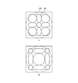
- FIG. 8 is a plan view showing a configuration example of a pixel according to a second embodiment of the present disclosure.
- FIG. 16 is a plan view showing a first configuration example of a pixel according to the third embodiment of the present disclosure.
- FIG. 16 is a plan view showing a second configuration example of the pixel according to the third embodiment of the present disclosure.
- FIG. 16 is a plan view showing a third configuration example of the pixel according to the third embodiment of the present disclosure.
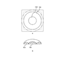
- FIG. 16 is a plan view showing a fourth configuration example of the pixel according to the third embodiment of the present disclosure.
- FIG. 16 is a plan view showing another configuration example of the pixel according to the fifth embodiment of the present disclosure.
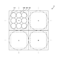
- FIG. 16 is a plan view showing a configuration example of a pixel array section according to a sixth embodiment of the present disclosure. It is a block diagram showing a schematic example of composition of a camera which is an example of an imaging device to which this art can be applied.
- FIG. 1 It is a figure which shows an example of a schematic structure of an endoscopic surgery system. It is a block diagram showing an example of functional composition of a camera head and CCU. It is a block diagram showing an example of a schematic structure of a vehicle control system. It is explanatory drawing which shows an example of the installation position of a vehicle exterior information detection part and an imaging part.
- FIG. 1 is a diagram illustrating a configuration example of an image sensor according to an embodiment of the present disclosure.
- the image sensor 1 shown in FIG. 1 includes a pixel array section 10, a vertical drive section 20, a column signal processing section 30, and a control section 40.
- the pixel array unit 10 is configured by arranging the pixels 100 in a two-dimensional lattice shape.
- the pixel 100 produces
- the pixel 100 has a photoelectric conversion unit that generates an electric charge according to the applied light.
- the pixel 100 further includes a pixel circuit. This pixel circuit generates an image signal based on the charges generated by the photoelectric conversion unit. Generation of the image signal is controlled by a control signal generated by the vertical drive unit 20 described later.
- signal lines 11 and 12 are arranged in an XY matrix.
- the signal line 11 is a signal line that transmits a control signal of a pixel circuit in the pixel 100, is arranged for each row of the pixel array unit 10, and is commonly wired to the pixels 100 arranged in each row.
- the signal line 12 is a signal line for transmitting an image signal generated by the pixel circuit of the pixel 100, is arranged for each column of the pixel array unit 10, and is commonly wired to the pixels 100 arranged in each column. It These photoelectric conversion units and pixel circuits are formed on a semiconductor substrate.
- the vertical drive unit 20 generates a control signal for the pixel circuit of the pixel 100.
- the vertical drive unit 20 transmits the generated control signal to the pixel 100 via the signal line 11 in the figure.
- the column signal processing unit 30 processes the image signal generated by the pixel 100.
- the column signal processing unit 30 processes the image signal transmitted from the pixel 100 via the signal line 12 in the figure.
- the processing in the column signal processing unit 30 corresponds to, for example, analog-digital conversion for converting an analog image signal generated in the pixel 100 into a digital image signal.
- the image signal processed by the column signal processing unit 30 is output as the image signal of the image sensor 1.
- the control unit 40 controls the entire image sensor 1.
- the control unit 40 controls the image sensor 1 by generating and outputting a control signal for controlling the vertical drive unit 20 and the column signal processing unit 30.
- the control signal generated by the control unit 40 is transmitted to the vertical drive unit 20 and the column signal processing unit 30 via the signal lines 41 and 42, respectively.
- the column signal processing unit 30 is an example of the processing circuit described in the claims.
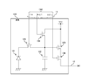
- FIG. 2 is a diagram showing a configuration example of a pixel according to the embodiment of the present disclosure.
- the figure is a circuit diagram showing a configuration example of the pixel 100.
- the pixel 100 shown in the figure includes a photoelectric conversion unit 101, a charge holding unit 102, and MOS transistors 103 to 106.
- the anode of the photoelectric conversion unit 101 is grounded, and the cathode is connected to the source of the MOS transistor 103.
- the drain of the MOS transistor 103 is connected to the source of the MOS transistor 104, the gate of the MOS transistor 105, and one end of the charge holding unit 102. The other end of the charge holding unit 102 is grounded.
- the drains of the MOS transistors 104 and 105 are commonly connected to the power supply line Vdd, and the source of the MOS transistor 105 is connected to the drain of the MOS transistor 106.
- the source of the MOS transistor 106 is connected to the signal line 12.
- the gates of the MOS transistors 103, 104 and 106 are connected to the transfer signal line TR, the reset signal line RST and the selection signal line SEL, respectively.
- the transfer signal line TR, the reset signal line RST, and the selection signal line SEL form the signal line 11.
- the photoelectric conversion unit 101 is to generate electric charges according to the irradiated light as described above.
- a photodiode can be used for the photoelectric conversion unit 101.
- the charge holding unit 102 and the MOS transistors 103 to 106 form a pixel circuit.
- the MOS transistor 103 is a transistor that transfers the charges generated by the photoelectric conversion of the photoelectric conversion unit 101 to the charge holding unit 102. The transfer of charges in the MOS transistor 103 is controlled by the signal transmitted through the transfer signal line TR.
- the charge holding unit 102 is a capacitor that holds the charges transferred by the MOS transistor 103.
- the MOS transistor 105 is a transistor that generates a signal based on the charges held in the charge holding unit 102.
- the MOS transistor 106 is a transistor that outputs the signal generated by the MOS transistor 105 to the signal line 12 as an image signal. The MOS transistor 106 is controlled by the signal transmitted by the selection signal line SEL.
- the MOS transistor 104 is a transistor that resets the charge holding unit 102 by discharging the charge held in the charge holding unit 102 to the power supply line Vdd.
- the reset by the MOS transistor 104 is controlled by the signal transmitted through the reset signal line RST, and is executed before the charge transfer by the MOS transistor 103.
- the photoelectric conversion unit 101 can also be reset by turning on the MOS transistor 103. In this way, the pixel circuit converts the charge generated by the photoelectric conversion unit 101 into an image signal.
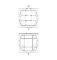
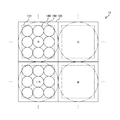
- FIG. 3 is a plan view showing a configuration example of a pixel according to the first embodiment of the present disclosure.
- the figure shows a configuration example of the pixels 100 arranged in the pixel array section 10.
- the solid line rectangle represents the pixel 100
- the dotted line rectangle represents the n-type semiconductor region 111 that constitutes the photoelectric conversion unit 101
- the two-dot chain line circle represents the on-chip lens 180
- the solid line circle represents the inside of the layer. This represents the lens 160.
- the on-chip lens 180 is a lens that is arranged in the outermost layer of the pixel 100 and focuses incident light from a subject on the photoelectric conversion unit 101.
- the in-layer lens 160 is a lens that is disposed between the on-chip lens 180 and the photoelectric conversion unit 101 and that further collects the incident light collected by the on-chip lens 180.
- a plurality of the in-layer lenses 160 are arranged for each pixel 100.
- the pixel 100 in the figure represents an example in which nine intra-layer lenses 160 are arranged in a grid pattern.
- a gap 169 is formed in the plurality of in-layer lenses 160 arranged. The incident light passing through the gap 169 is applied to the photoelectric conversion unit 101 without passing through the in-layer lens 160. Details of the configuration of the pixel 100 will be described later.
- a color filter 172 (not shown) is arranged in the pixel 100.
- the color filter 172 is an optical filter that transmits light having a predetermined wavelength of incident light.
- a color filter that transmits red light, green light, and blue light can be arranged in each pixel 100.
- the characters in the figure represent the type of the color filter 172 arranged in the pixel 100. Specifically, “R”, “G”, and “B” indicate that the color filters 172 corresponding to red light, green light, and blue light are arranged, respectively.
- These color filters 172 can be arranged in a Bayer array, for example.
- the Bayer array is an array method in which the color filters 172 corresponding to green light are arranged in a checkered pattern, and the color filters 172 corresponding to red light and blue light are arranged between the color filters 172 corresponding to green light.
- the pixel array unit 10 is configured by arranging four pixels 100 arranged in two rows and two columns shown in FIG.
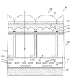
- FIG. 4 is a cross-sectional view showing a configuration example of a pixel according to the embodiment of the present disclosure.
- the figure is a cross-sectional view showing a configuration example of the pixel 100 arranged in the pixel array section 10.
- 3 is a sectional view of the image sensor 1 (pixel array unit 10) taken along the line AA′ in FIG.
- the pixel 100 shown in FIG. 1 includes a semiconductor substrate 110, a wiring region 130, a support substrate 140, an insulating film 120, a light shielding film 150, an in-layer lens 160, a flattening film 171, a color filter 172, an on-state. And a chip lens 180.
- the semiconductor substrate 110 is a semiconductor substrate in which semiconductor regions of the elements forming the pixel circuit described in FIG. 2 are formed.
- the semiconductor substrate 110 in the figure includes a p-type semiconductor region 112 forming a well region and an n-type semiconductor region 111 formed inside the p-type semiconductor region 112.
- the photoelectric conversion unit 101 is configured by the n-type semiconductor region 111.
- the pn junction between the n-type semiconductor region 111 and the p-type semiconductor region 112 around the n-type semiconductor region 111 operates as a photodiode. When the pn junction is irradiated with incident light, charges are generated by photoelectric conversion and accumulated in the n-type semiconductor region 111.
- the MOS transistor 103 in the figure is a MOS transistor having the n-type semiconductor region 111 as a source region and the p-type semiconductor region 112 as a channel region.
- the MOS transistor 103 includes a gate electrode 133.
- the semiconductor substrate 110 can be made of, for example, silicon (Si). Further, the vertical driving unit 20 and the like described in FIG. 1 can be arranged on the semiconductor substrate 110.
- the wiring region 130 is a region where a wiring formed on the surface of the semiconductor substrate 110 and electrically connecting the semiconductor elements formed on the semiconductor substrate 110 is formed.
- a wiring layer 132 and an insulating layer 131 are arranged in the wiring region 130.
- the wiring layer 132 constitutes the above-mentioned wiring.
- the wiring layer 132 can be formed of, for example, copper (Cu) or tungsten (W).
- the insulating layer 131 insulates the wiring layer 132.
- the insulating layer 131 can be made of, for example, silicon oxide (SiO 2 ) or silicon nitride (SiN).
- the gate electrode 133 described above is further arranged in the wiring region 130.
- the support substrate 140 is a substrate that supports the image sensor 1.
- the support substrate 140 is a substrate that is formed of a semiconductor wafer or the like and mainly improves the strength of the image pickup device 1 when the image pickup device 1 is manufactured.
- the insulating film 120 is a film that insulates and protects the back surface side of the semiconductor substrate 110.
- the insulating film 120 can be made of an oxide such as SiO 2 .
- the light-shielding film 150 is a film which is arranged near the boundary between the pixels 100 and shields incident light obliquely incident from the adjacent pixels 100. As described with reference to FIG. 3, the color filters 172 corresponding to different lights are arranged in the adjacent pixels 100. When the photoelectric conversion unit 101 is irradiated with incident light that has passed through different types of color filters 172 of the adjacent pixels 100, color mixing occurs, and the image quality deteriorates. This color mixing can be prevented by disposing the light shielding film 150 and shielding the incident light from the adjacent pixels 100.
- the light blocking film 150 has an opening 151 in the center of the pixel 100. Incident light is applied to the photoelectric conversion unit 101 through the opening 151.
- the light shielding film 150 for example, a film made of W can be used.
- the in-layer lens 160 is a lens that is formed in the inner layer of the pixel 100 and collects incident light.
- the hemispherical convex portion in the figure corresponds to one in-layer lens 160.
- the plurality of in-layer lenses 160 are arranged in the pixel 100. These in-layer lenses 160 are arranged in parallel to the optical path of incident light in the pixel 100. Specifically, the plurality of in-layer lenses 160 are arranged so that the incident light that has passed through one of the in-layer lenses 160 reaches the photoelectric conversion unit 101. The incident light reaches the photoelectric conversion unit 101 without passing through the plurality of intralayer lenses 160.
- the plurality of in-layer lenses 160 are arranged in substantially the same layer.
- the intralayer lenses 160 When the intralayer lenses 160 are arranged in the same layer as described above, the intralayer lenses 160 can be formed at the same time. It should be noted that the plurality of inner lenses 160 can be formed in different layers as long as the incident light transmitted through one of the plurality of inner lenses 160 reaches the photoelectric conversion unit 101. ..
- the intralayer lens 160 can be made of a high refractive index inorganic material or resin.
- the intralayer lens 160 can be made of SiN or silicon oxynitride (SiON).
- each of the intralayer lenses 160 can be configured to have a diameter of 0.8 ⁇ m to 1.0 ⁇ m, for example.
- the in-layer lens 160 in the figure represents an example in which the lower layer portion is formed of a common film. The lower part of the intralayer lens 160 flattens the back surface of the image sensor 1 on which the light shielding film 150 is formed.
- the flattening film 171 is for flattening the back surface of the image pickup device 1 on which the in-layer lens 160 is formed.
- the flattening film 171 can be made of resin, for example.
- the color filter 172 and the on-chip lens 180 are stacked on the flattening film 171.
- the image pickup device 1 in the figure corresponds to a backside illumination type image pickup device in which incident light is emitted from the backside of the semiconductor substrate 110.
- Solid arrows in the figure represent the incident light emitted from the back surface.
- the incident light transmitted through the on-chip lens 180 and the in-layer lens 160 reaches the n-type semiconductor region 111 of the semiconductor substrate 110, and photoelectric conversion is performed.
- a part of the light incident on the semiconductor substrate 110 passes through the semiconductor substrate 110 without contributing to photoelectric conversion and reaches the wiring region 130.
- the dashed arrows in the figure show how incident light passes through the semiconductor substrate 110. When this transmitted light is reflected by the wiring layer 132 and emitted to the outside of the pixel 100, it becomes stray light.
- a plurality of in-layer lenses 160 are arranged to reduce the reflected light from the wiring layer 132.
- FIG. 5 is a diagram showing an optical path of incident light in a pixel according to a conventional technique.
- this figure is a diagram showing an optical path of incident light in a pixel in which one in-layer lens 160 is arranged.
- the on-chip lens 180, the in-layer lens 160, the n-type semiconductor region 111, and the wiring layer 132 are shown. It is a figure showing the outline of. Solid arrows in the figure represent incident light having a relatively long wavelength such as red light, and dotted arrows represent incident light having a relatively short wavelength such as blue light.
- These incident lights are condensed by the on-chip lens 180 and the in-layer lens 160 and reach the photoelectric conversion unit 101 (n-type semiconductor region 111).
- the focal length is shortened and the height of the image sensor 1 can be reduced.
- the incident light is not absorbed in the n-type semiconductor region 111, that is, when photoelectric conversion is not performed, the incident light is transmitted through the n-type semiconductor region 111, reaches the wiring layer 132 of the wiring region 130, and is reflected.
- the incident light having a relatively short wavelength is focused on the shallow position of the n-type semiconductor region 111. If it is not absorbed in the n-type semiconductor region 111, it diffuses and reaches the wiring layer 132 in the wiring region 130. On the other hand, the incident light having a relatively long wavelength has a focal point formed at a deep position in the n-type semiconductor region 111. For this reason, when the incident light having a relatively long wavelength is not absorbed in the n-type semiconductor region 111, it reaches the wiring layer 132 and is reflected while being concentrated in a relatively narrow range as shown by a dashed arrow. For this reason, the longer the wavelength of the incident light, the stronger the reflection.
- FIG. 6 is a diagram showing an example of an optical path of incident light in the pixel according to the first embodiment of the present disclosure.
- Incident light transmitted through the on-chip lens 180 in the figure is condensed by a plurality of (in the figure, three) intralayer lenses 160a, 160b, and 160c, and is irradiated onto the n-type semiconductor region 111. Further, the incident light applied to the region where the two in-layer lenses 160 are in contact with each other is repeatedly reflected between the two in-layer lenses 160 and then applied to the n-type semiconductor region 111. In this way, the incident light is dispersed by the in-layer lens 160 and applied to the n-type semiconductor region 111.
- the wiring layer 132 When the incident light is not absorbed in the n-type semiconductor region 111, it reaches the wiring layer 132 in a widely dispersed state, and the reflected light can be reduced. Further, since the incident light is dispersed, the degree of freedom in the layout of the wiring layer 132 can be improved.
- the wiring layer 132 may be arranged immediately below the central portion of the photoelectric conversion unit 101.
- one of the plurality of intra-layer lenses 160 is arranged in the central portion of the pixel 100, as in the intra-layer lens 160b of FIG. Specifically, one of the plurality of in-layer lenses 160 is arranged on the optical axis of the on-chip lens 180. Since the incident light transmitted through the on-chip lens 180 is collected in the central portion of the pixel 100, a large amount of incident light transmitted through the on-chip lens 180 can be transmitted to the intralayer lens 160. The incident light can be more dispersed as compared with the case where the gap 169 is arranged on the optical axis of the on-chip lens 180.
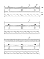
- FIGS. 7 and 8 are diagrams showing an example of a method for manufacturing an image sensor according to the embodiment of the present disclosure.
- the figure shows an example of a manufacturing process of the image sensor 1.
- the configuration of the pixel 100 is simplified and described.
- the wiring region 130 is formed on the semiconductor substrate 110 on which the p-type semiconductor region 112 and the n-type semiconductor region 111 are formed.
- the support substrate 140 is bonded, the top and bottom of the semiconductor substrate 110 are inverted, and the back surface of the semiconductor substrate 110 is ground to reduce the thickness.
- the insulating film 120 and the light shielding film 150 are arranged on the back surface of the semiconductor substrate 110 (A in FIG. 7).
- the lens material 401 which is the material of the in-layer lens 160, is arranged on the back surface of the semiconductor substrate 110.
- This can be formed, for example, by forming a lens material such as SiN using CVD (Chemical Vapor Deposition) or the like (B in FIG. 7).
- a resist 402 is laminated on the lens material 401.
- a photoresist may be used as the resist 402, and the resist 402 can be formed by applying the photoresist on the lens material 401 (C in FIG. 7).
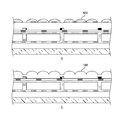
- a resist 403 having the same shape as the intralayer lens 160 is formed.
- the resist 402 is patterned into a cylindrical or cubic shape by, for example, a lithography technique. Then, it can be formed by dissolving the patterned resist 402 using a reflow oven or the like (D in FIG. 8).
- the plurality of in-layer lenses 160 are arranged to disperse the incident light that has passed through the on-chip lens 180 and to convert the photoelectric conversion unit 101. To irradiate. Thereby, the reflected light from the wiring layer 132 can be reduced and the deterioration of the image quality can be prevented.
- Second Embodiment> In the image sensor 1 of the above-described first embodiment, nine intra-layer lenses 160 are arranged. On the other hand, the image sensor 1 according to the second embodiment of the present disclosure is different from the above-described first embodiment in that a different number of intralayer lenses 160 are arranged.
- FIG. 9 is a plan view showing a configuration example of a pixel according to the second embodiment of the present disclosure. Similar to FIG. 3, this figure is a diagram showing a configuration example of the pixel 100. Hereinafter, as for the same components as those in FIG. 3, the reference numerals are omitted.
- a in the figure represents an example in which four intra-layer lenses 160 are arranged.
- B in the figure represents an example in which 16 in-layer lenses 160 are arranged.
- any number of two or more intralayer lenses 160 can be arranged in the pixel 100.
- the gap 169 between the intralayer lenses 160 can be made smaller, and more incident light can be dispersed. It is possible to arrange the number of the intralayer lenses 160 according to the processing accuracy of the intralayer lenses 160 in the manufacturing process of the image sensor 1.
- C in the figure shows an example of a case where nine in-layer lenses 160 each having a relatively small diameter are arranged near the center of the pixel 100. Even in this case, the gap 169 can be reduced.
- the configuration of the image sensor 1 other than this is the same as the configuration of the image sensor 1 described in the first embodiment of the present disclosure, and thus the description thereof will be omitted.
- two or more arbitrary intralayer lenses 160 can be arranged according to the processing accuracy.
- the circular inner lens 160 is arranged in a plan view.
- the image sensor 1 according to the third embodiment of the present disclosure is different from the above-described first embodiment in that an intralayer lens having a different shape is arranged.
- FIG. 10 is a plan view showing a first configuration example of a pixel according to the third embodiment of the present disclosure.
- This figure is a diagram showing a configuration example of the pixel 100 similarly to FIG. 3.
- the pixel 100 is different from the pixel 100 described in FIG. 3 in that an intralayer lens having a shape other than the circular shape is arranged.
- a in the figure shows an example in which, in addition to the intralayer lens 160, an intralayer lens 161 having an elliptical shape in plan view is arranged.
- B in the figure shows another arrangement example of the intralayer lenses 160 and 161. In this way, the intralayer lenses 160 and 161 having different shapes can be arranged in the pixel 100.
- FIG. 11 is a plan view showing a second configuration example of the pixel according to the third embodiment of the present disclosure.
- This figure shows an example in which the inner lens 161 or the inner lenses 160 and 161 are arranged and the size is optimized so as to reduce the gap 169.
- a in the figure shows an example in which two in-layer lenses 161 are arranged.
- B and C in the figure represent an example in which the intralayer lenses 160 and 161 are arranged.
- the gap 169 can be made narrower than the arrangement of the intralayer lenses 160 and 161 shown in FIG.
- FIG. 12 is a plan view showing a third configuration example of the pixel according to the third embodiment of the present disclosure.
- the figure shows an example in which a rectangular inner lens 162 is arranged in a plan view.
- B in the figure shows an example of a case where the intralayer lenses 162 having a square shape and a rectangular shape in a plan view are combined and arranged.
- FIG. 13 is a plan view showing a fourth configuration example of the pixel according to the third embodiment of the present disclosure.
- a in the figure shows an example in which the intralayer lens 163 and the intralayer lens 160 are arranged
- B in the figure shows the cross-sectional shape of the intralayer lens.
- the inner-layer lens 163 is an inner-layer lens having an opening in the central portion in a plan view, and is an inner-layer lens having a shape obtained by dividing an annular body in two in the thickness direction.
- the in-layer lens 160 in the figure is arranged in the opening of the in-layer lens 163. As described above, by arranging the intralayer lenses 160 and 163 in combination, the gap 169 can be made smaller.
- the configuration of the image sensor 1 other than this is the same as the configuration of the image sensor 1 described in the first embodiment of the present disclosure, and thus the description thereof will be omitted.
- the gaps 169 can be made smaller by arranging the intralayer lenses 160 to 163 having different shapes, and more incident light can be obtained. Can be dispersed.
- the image sensor 1 of the above-described first embodiment uses the intralayer lens 160 that is symmetrically arranged with respect to the center of the pixel 100.
- the image sensor 1 according to the fourth embodiment of the present disclosure is different from the above-described first embodiment in that an intralayer lens that is asymmetrically arranged with respect to the center of the pixel 100 is used.
- FIG. 14 is a plan view showing a configuration example of a pixel according to the fourth embodiment of the present disclosure.
- This figure is a diagram showing a configuration example of the pixel 100 similarly to FIG. 3.
- the pixel shown in the figure is different from the pixel 100 described in FIG. 3 in that the arrangement of the in-layer lens is arranged asymmetrically with respect to the center of the pixel.
- the pixels (pixels 201 and 202) in the figure represent an example in which four intra-layer lenses 161 having different sizes are arranged. Specifically, in the pixel shown in the figure, two relatively large in-layer lenses 161a and two relatively small in-layer lenses 161b are arranged.
- the in-layer lens 161 is arranged in an asymmetrical shape with respect to the center of the pixel 100, and the dispersion of incident light can be asymmetrical.
- the pixel 201 of A in the figure and the pixel 202 of B in the figure are configured by changing the arrangement of the intralayer lenses 161a and 161b by 180 degrees. These pixels 201 and 202 are arranged at the ends of the pixel array section 10 described with reference to FIG. Specifically, the pixel 201 of A in the figure is arranged at the right end of the pixel array section 10, and the pixel 202 of B in the figure is arranged at the left end of the pixel array section 10. Incident light is obliquely applied to the pixels at the ends of the pixel array unit 10 according to the image height of the subject. Therefore, the influence of the image height can be reduced by arranging the intralayer lens 161 asymmetrically.
- FIG. 15 is a diagram showing an example of an optical path of incident light in a pixel according to the fourth embodiment of the present disclosure.
- the figure shows the optical path of incident light in the pixel 201.
- the pixel 201 is arranged at the right end of the pixel array section 10. Therefore, the incident light on the pixel 201 is obliquely incident from the upper left of the drawing. Therefore, a plurality of in-layer lenses 161 are arranged transitioning to the right side of the figure in the pixel 201, and the left in-layer lens 161 is horizontally long. Thereby, the oblique incident light can be condensed and dispersed in the central portion of the pixel 201.
- the configuration of the image sensor 1 other than this is the same as the configuration of the image sensor 1 described in the first embodiment of the present disclosure, and thus the description thereof will be omitted.
- the image sensor 1 includes the in-layer lens that is arranged asymmetrically with respect to the center of the pixel, so that the incident light that enters obliquely is incident on the central portion of the pixel. It is possible to collect the light on the surface and disperse it in the pixel.
- the intralayer lens 160 is arranged in all the pixels 100 of the pixel array section 10.
- the in-layer lens 160 is arranged in the pixel 100 in which the color filter 172 corresponding to the long-wavelength incident light is arranged, and therefore, the above-described first embodiment. This is different from the first embodiment.
- FIG. 16 is a plan view showing a configuration example of a pixel according to the fifth embodiment of the present disclosure.
- the pixel 100 shown in the figure is different from the pixel 100 described in FIG. 3 in that the in-layer lens 160 is arranged in the pixel 100 in which the color filter 172 corresponding to red light is arranged. Since red light has a long wavelength as described above, it reaches a deep portion of the semiconductor substrate 110. Therefore, the light reflected by the wiring layer 132 increases. On the other hand, green light or blue light having a short wavelength is condensed in a relatively shallow region of the semiconductor substrate 110. Therefore, the light reflected by the wiring layer 132 is relatively small.
- the in-layer lens 160 is arranged in the pixel 100 in which the color filter 172 corresponding to red light is arranged, and the in-layer lens 160 of the pixel 100 in which the color filter 172 corresponding to green light and blue light is arranged is omitted. .. Thereby, the configuration of the image sensor 1 can be simplified.
- FIG. 17 is a plan view showing another configuration example of the pixel according to the fifth embodiment of the present disclosure.
- the figure is different from the pixel 100 described in FIG. 3 in that the pixel 100 further includes a pixel 100 in which a color filter 172 corresponding to infrared light is arranged.
- the color filter 172 corresponding to the infrared light is the color filter 172 that transmits infrared light.
- the pixel 100 with "IR" indicates the color filter 172 corresponding to infrared light.
- the pixel 100 in which the color filter 172 corresponding to infrared light is arranged can be assigned to one of the pixels 100 in which the color filters 172 corresponding to two green light in the Bayer array are arranged. Even in the pixel 100 in which the color filter 172 corresponding to infrared light having a long wavelength is arranged, the in-layer lens 160 can be arranged to disperse the incident light.
- the configuration of the image sensor 1 other than this is the same as the configuration of the image sensor 1 described in the first embodiment of the present disclosure, and thus the description thereof will be omitted.
- the image pickup device 1 simplifies the configuration of the image pickup device 1 by disposing the intralayer lens 160 in the pixel according to the wavelength of the incident light. You can
- the image sensor 1 of the above-described first embodiment only the pixels 100 are arranged in the pixel array section 10.
- the image sensor 1 according to the sixth embodiment of the present disclosure is different from the above-described first embodiment in that phase difference pixels for detecting the image plane phase difference of the subject are further arranged. different.
- FIG. 18 is a plan view showing a configuration example of a pixel array section according to the sixth embodiment of the present disclosure.
- the pixel array unit 10 in the figure is different from the pixel array unit 10 described in FIG. 3 in that a phase difference pixel 300 is arranged in addition to the pixel 100.
- the phase difference pixel 300 is a pixel for detecting the image plane phase difference of the subject.
- the image pickup device 1 is used together with a photographing lens arranged outside, and an image of a subject is formed on the pixel array section 10 of the image pickup device 1 by the photographing lens. By detecting the phase difference of the imaged subject at this time, the focus position of the subject can be detected, and autofocus for adjusting the position of the photographing lens can be performed.
- the arrangement of the light shielding film 150 is described.
- the light shielding film 150 having the opening 152 is arranged instead of the opening 151.
- the phase difference pixel 300 is arranged so that the light shielding film 150 covers the left half or the right half of the photoelectric conversion unit 101.
- the phase difference pixels 300a and 300b the left half and the right half of the photoelectric conversion unit 101 are shielded from light by the light shielding film 150, respectively.
- the incident light transmitted through the left side and the right side of the taking lens respectively reaches the photoelectric conversion unit 101, and respective image signals are generated.
- Such processing is called pupil division.
- phase difference pixels 300a and 300b are arranged in the pixel array section 10. Two images are generated based on the respective image signals generated by the plurality of phase difference pixels 300a and 300b. Next, the focus position of the photographing lens can be detected by detecting the phase difference between these two images.
- phase difference pixels 300 the accuracy of pupil division can be improved by omitting the intralayer lens 160. This is because the incident light associated with pupil division is not dispersed by the intralayer lens 160. It is possible to reduce the error in detecting the phase difference.
- the configuration of the image sensor 1 other than this is the same as the configuration of the image sensor 1 described in the first embodiment of the present disclosure, and thus the description thereof will be omitted.
- the incident light in the pixel 100 is dispersed and an error in the phase difference detection by the phase difference pixel 300 is detected. Can be reduced.
- the technology according to the present disclosure (this technology) can be applied to various products.
- the present technology may be realized as an image pickup device mounted on an image pickup apparatus such as a camera.
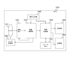
- FIG. 19 is a block diagram showing a schematic configuration example of a camera which is an example of an imaging device to which the present technology can be applied.
- the camera 1000 in the figure includes a lens 1001, an image sensor 1002, an image capture controller 1003, a lens driver 1004, an image processor 1005, an operation input unit 1006, a frame memory 1007, and a display unit 1008. And a recording unit 1009.
- the lens 1001 is a taking lens of the camera 1000.
- the lens 1001 collects light from a subject and makes it incident on an image sensor 1002 described later to form an image of the subject.
- the image pickup element 1002 is a semiconductor element that picks up the light from the subject condensed by the lens 1001.
- the image sensor 1002 generates an analog image signal according to the emitted light, converts it into a digital image signal, and outputs it.
- the image capturing control unit 1003 controls image capturing by the image sensor 1002.
- the imaging control unit 1003 controls the imaging element 1002 by generating a control signal and outputting the control signal to the imaging element 1002.
- the imaging control unit 1003 can also perform autofocus in the camera 1000 based on the image signal output from the image sensor 1002.
- the auto focus is a system that detects the focal position of the lens 1001 and automatically adjusts it.
- a method (image plane phase difference autofocus) of detecting a focus position by detecting an image plane phase difference by a phase difference pixel arranged in the image sensor 1002 can be used. It is also possible to apply a method (contrast autofocus) of detecting the position where the contrast of the image is the highest as the focus position.
- the imaging control unit 1003 adjusts the position of the lens 1001 via the lens driving unit 1004 based on the detected focal position, and performs autofocus.
- the imaging control unit 1003 can be configured by, for example, a DSP (Digital Signal Processor) equipped with firmware.
- DSP Digital Signal Processor
- the lens driving unit 1004 drives the lens 1001 under the control of the imaging control unit 1003.
- the lens driving unit 1004 can drive the lens 1001 by changing the position of the lens 1001 using a built-in motor.
- the image processing unit 1005 processes the image signal generated by the image sensor 1002. This processing includes, for example, demosaic for generating image signals of insufficient colors among the image signals corresponding to red, green and blue for each pixel, noise reduction for removing noise of the image signals and encoding of the image signals. Applicable
- the image processing unit 1005 can be configured by, for example, a microcomputer equipped with firmware.
- the operation input unit 1006 receives an operation input from the user of the camera 1000.
- this operation input unit 1006 for example, a push button or a touch panel can be used.
- the operation input received by the operation input unit 1006 is transmitted to the imaging control unit 1003 and the image processing unit 1005. After that, processing according to the operation input, for example, processing such as imaging of a subject is started.
- the frame memory 1007 is a memory that stores a frame that is an image signal for one screen.
- the frame memory 1007 is controlled by the image processing unit 1005 and holds a frame in the process of image processing.
- the display unit 1008 displays the image processed by the image processing unit 1005.
- a liquid crystal panel can be used for the display unit 1008.
- the recording unit 1009 records the image processed by the image processing unit 1005.
- a memory card or a hard disk can be used.
- the present technology can be applied to the image sensor 1002 among the configurations described above.
- the image sensor 1 described with reference to FIG. 1 can be applied to the image sensor 1002.
- the image processing unit 1005 is an example of the processing circuit described in the claims.
- the camera 1000 is an example of the imaging device described in the claims.
- the camera has been described as an example, but the technology according to the present disclosure may be applied to, for example, a monitoring device and the like.
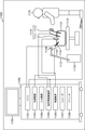
- FIG. 20 is a diagram showing an example of a schematic configuration of an endoscopic surgery system to which the technology according to the present disclosure (the present technology) can be applied.
- FIG. 20 illustrates a situation in which an operator (doctor) 11131 is performing an operation on a patient 11132 on a patient bed 11133 using the endoscopic operation system 11000.
- the endoscopic surgery system 11000 includes an endoscope 11100, other surgical tools 11110 such as a pneumoperitoneum tube 11111 and an energy treatment tool 11112, and a support arm device 11120 that supports the endoscope 11100.
- a cart 11200 on which various devices for endoscopic surgery are mounted.
- the endoscope 11100 includes a lens barrel 11101 into which a region having a predetermined length from the distal end is inserted into the body cavity of the patient 11132, and a camera head 11102 connected to the base end of the lens barrel 11101.
- the endoscope 11100 configured as a so-called rigid endoscope having the rigid barrel 11101 is illustrated, but the endoscope 11100 may be configured as a so-called flexible mirror having a flexible barrel. Good.
- An opening in which an objective lens is fitted is provided at the tip of the lens barrel 11101.
- a light source device 11203 is connected to the endoscope 11100, and the light generated by the light source device 11203 is guided to the tip of the lens barrel by a light guide extending inside the lens barrel 11101. It is irradiated toward the observation target in the body cavity of the patient 11132 via the lens.
- the endoscope 11100 may be a direct-viewing endoscope, or may be a perspective or side-viewing endoscope.
- An optical system and an image pickup device are provided inside the camera head 11102, and reflected light (observation light) from an observation target is condensed on the image pickup device by the optical system.
- the observation light is photoelectrically converted by the imaging element, and an electric signal corresponding to the observation light, that is, an image signal corresponding to the observation image is generated.
- the image signal is transmitted to the camera control unit (CCU: 11201) as RAW data.
- the CCU 11201 is composed of a CPU (Central Processing Unit), a GPU (Graphics Processing Unit), and the like, and controls the operations of the endoscope 11100 and the display device 11202 in a centralized manner. Further, the CCU 11201 receives the image signal from the camera head 11102, and performs various image processing such as development processing (demosaic processing) on the image signal for displaying an image based on the image signal.
- image processing such as development processing (demosaic processing)
- the display device 11202 displays an image based on an image signal subjected to image processing by the CCU 11201 under the control of the CCU 11201.
- the light source device 11203 is composed of a light source such as an LED (Light Emitting Diode), and supplies irradiation light to the endoscope 11100 when photographing an operation site or the like.
- a light source such as an LED (Light Emitting Diode)
- LED Light Emitting Diode
- the input device 11204 is an input interface for the endoscopic surgery system 11000.
- the user can input various kinds of information and instructions to the endoscopic surgery system 11000 via the input device 11204.
- the user inputs an instruction to change the imaging conditions (type of irradiation light, magnification, focal length, etc.) by the endoscope 11100.
- the treatment instrument control device 11205 controls driving of the energy treatment instrument 11112 for cauterization of tissue, incision, sealing of blood vessel, or the like.
- the pneumoperitoneum device 11206 is used to inflate the body cavity of the patient 11132 through the pneumoperitoneum tube 11111 in order to inflate the body cavity of the patient 11132 for the purpose of securing the visual field by the endoscope 11100 and the working space of the operator.
- the recorder 11207 is a device capable of recording various information regarding surgery.
- the printer 11208 is a device capable of printing various types of information regarding surgery in various formats such as text, images, and graphs.
- the light source device 11203 that supplies irradiation light to the endoscope 11100 when imaging a surgical site can be configured by, for example, an LED, a laser light source, or a white light source configured by a combination thereof.
- a white light source is formed by a combination of RGB laser light sources
- the output intensity and output timing of each color (each wavelength) can be controlled with high accuracy, so that the light source device 11203 adjusts the white balance of the captured image. It can be carried out.
- the laser light from each of the RGB laser light sources is irradiated on the observation target in a time division manner, and the drive of the image pickup device of the camera head 11102 is controlled in synchronization with the irradiation timing so as to correspond to each of the RGB. It is also possible to take the captured image in a time division manner. According to this method, a color image can be obtained without providing a color filter on the image sensor.
- the drive of the light source device 11203 may be controlled so as to change the intensity of the output light at predetermined time intervals.
- the drive of the image sensor of the camera head 11102 in synchronization with the timing of changing the intensity of the light to acquire an image in a time-division manner and combining the images, a high dynamic image without so-called blackout and blown-out highlights is obtained. An image of the range can be generated.
- the light source device 11203 may be configured to be able to supply light in a predetermined wavelength band corresponding to special light observation.
- special light observation for example, by utilizing the wavelength dependence of the absorption of light in body tissues, by irradiating a narrow band of light as compared with the irradiation light (that is, white light) during normal observation, the mucosal surface layer
- the so-called narrow band imaging is performed in which a predetermined tissue such as blood vessels is imaged with high contrast.
- fluorescence observation in which an image is obtained by fluorescence generated by irradiating the excitation light may be performed.
- the body tissue is irradiated with excitation light to observe fluorescence from the body tissue (autofluorescence observation), or a reagent such as indocyanine green (ICG) is locally injected into the body tissue and the body tissue is injected.
- the excitation light corresponding to the fluorescence wavelength of the reagent can be irradiated to obtain a fluorescence image.
- the light source device 11203 can be configured to be capable of supplying narrowband light and/or excitation light compatible with such special light observation.
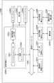
- FIG. 21 is a block diagram showing an example of the functional configuration of the camera head 11102 and the CCU 11201 shown in FIG.
- the camera head 11102 includes a lens unit 11401, an imaging unit 11402, a driving unit 11403, a communication unit 11404, and a camera head control unit 11405.
- the CCU 11201 has a communication unit 11411, an image processing unit 11412, and a control unit 11413.
- the camera head 11102 and the CCU 11201 are communicably connected to each other by a transmission cable 11400.
- the lens unit 11401 is an optical system provided at the connecting portion with the lens barrel 11101.
- the observation light taken in from the tip of the lens barrel 11101 is guided to the camera head 11102 and enters the lens unit 11401.
- the lens unit 11401 is configured by combining a plurality of lenses including a zoom lens and a focus lens.
- the image pickup unit 11402 is composed of an image pickup element.
- the number of image pickup elements forming the image pickup section 11402 may be one (so-called single-plate type) or plural (so-called multi-plate type).
- image signals corresponding to R, G, and B may be generated by the respective image pickup elements, and these may be combined to obtain a color image.
- the image capturing unit 11402 may be configured to have a pair of image capturing elements for respectively acquiring image signals for the right eye and the left eye corresponding to 3D (Dimensional) display.
- the 3D display enables the operator 11131 to more accurately understand the depth of the living tissue in the operation site.
- a plurality of lens units 11401 may be provided corresponding to each image pickup element.
- the image pickup unit 11402 does not necessarily have to be provided on the camera head 11102.
- the imaging unit 11402 may be provided inside the lens barrel 11101 immediately after the objective lens.
- the drive unit 11403 is composed of an actuator, and moves the zoom lens and the focus lens of the lens unit 11401 by a predetermined distance along the optical axis under the control of the camera head control unit 11405. Accordingly, the magnification and focus of the image captured by the image capturing unit 11402 can be adjusted appropriately.
- the communication unit 11404 is composed of a communication device for transmitting and receiving various information to and from the CCU11201.
- the communication unit 11404 transmits the image signal obtained from the imaging unit 11402 as RAW data to the CCU 11201 via the transmission cable 11400.
- the communication unit 11404 receives a control signal for controlling the driving of the camera head 11102 from the CCU 11201 and supplies it to the camera head control unit 11405.
- the control signal includes, for example, information that specifies the frame rate of the captured image, information that specifies the exposure value at the time of capturing, and/or information that specifies the magnification and focus of the captured image. Contains information about the condition.
- the image capturing conditions such as the frame rate, the exposure value, the magnification, and the focus may be appropriately designated by the user, or may be automatically set by the control unit 11413 of the CCU 11201 based on the acquired image signal. Good. In the latter case, the so-called AE (Auto Exposure) function, AF (Auto Focus) function, and AWB (Auto White Balance) function are installed in the endoscope 11100.
- AE Auto Exposure
- AF Auto Focus
- AWB Auto White Balance
- the camera head control unit 11405 controls driving of the camera head 11102 based on a control signal from the CCU 11201 received via the communication unit 11404.
- the communication unit 11411 is composed of a communication device for transmitting and receiving various information to and from the camera head 11102.
- the communication unit 11411 receives the image signal transmitted from the camera head 11102 via the transmission cable 11400.
- the communication unit 11411 transmits a control signal for controlling the driving of the camera head 11102 to the camera head 11102.
- the image signal and the control signal can be transmitted by electric communication, optical communication, or the like.
- the image processing unit 11412 performs various kinds of image processing on the image signal that is the RAW data transmitted from the camera head 11102.
- the control unit 11413 performs various controls regarding imaging of a surgical site or the like by the endoscope 11100 and display of a captured image obtained by imaging the surgical site or the like. For example, the control unit 11413 generates a control signal for controlling the driving of the camera head 11102.
- control unit 11413 causes the display device 11202 to display a captured image of the surgical site or the like based on the image signal subjected to the image processing by the image processing unit 11412.
- the control unit 11413 may recognize various objects in the captured image using various image recognition techniques.
- the control unit 11413 detects a surgical instrument such as forceps, a specific living body part, bleeding, and a mist when the energy treatment instrument 11112 is used by detecting the shape and color of the edge of the object included in the captured image. Can be recognized.
- the control unit 11413 may use the recognition result to superimpose and display various types of surgery support information on the image of the operation unit. By displaying the surgery support information in a superimposed manner and presenting it to the operator 11131, the burden on the operator 11131 can be reduced and the operator 11131 can surely proceed with the surgery.
- the transmission cable 11400 that connects the camera head 11102 and the CCU 11201 is an electric signal cable that supports electric signal communication, an optical fiber that supports optical communication, or a composite cable of these.
- wired communication is performed using the transmission cable 11400, but communication between the camera head 11102 and the CCU 11201 may be performed wirelessly.
- the technology according to the present disclosure can be applied to the imaging unit 11402 among the configurations described above.
- the image pickup device 1 of FIG. 1 can be applied to the image pickup unit 10402.
- the technology according to the present disclosure can be applied to the image capturing unit 10402, so that the surgeon can surely confirm the surgical region.
- the endoscopic surgery system has been described as an example, but the technology according to the present disclosure may be applied to, for example, a microscopic surgery system or the like.
- the technology according to the present disclosure (this technology) can be applied to various products.
- the technology according to the present disclosure is realized as a device mounted on any type of moving body such as an automobile, an electric vehicle, a hybrid electric vehicle, a motorcycle, a bicycle, a personal mobility, an airplane, a drone, a ship, and a robot. May be.
- FIG. 22 is a block diagram showing a schematic configuration example of a vehicle control system that is an example of a mobile body control system to which the technology according to the present disclosure can be applied.
- the vehicle control system 12000 includes a plurality of electronic control units connected via a communication network 12001.
- the vehicle control system 12000 includes a drive system control unit 12010, a body system control unit 12020, a vehicle exterior information detection unit 12030, a vehicle interior information detection unit 12040, and an integrated control unit 12050.
- a microcomputer 12051, an audio/video output unit 12052, and an in-vehicle network I/F (interface) 12053 are shown as a functional configuration of the integrated control unit 12050.
- the drive system control unit 12010 controls the operation of devices related to the drive system of the vehicle according to various programs.
- the drive system control unit 12010 includes a drive force generation device for generating a drive force of a vehicle such as an internal combustion engine or a drive motor, a drive force transmission mechanism for transmitting the drive force to wheels, and a steering angle of the vehicle. It functions as a steering mechanism for adjusting and a control device such as a braking device for generating a braking force of the vehicle.
- the body system control unit 12020 controls operations of various devices mounted on the vehicle body according to various programs.
- the body system control unit 12020 functions as a keyless entry system, a smart key system, a power window device, or a control device for various lamps such as a head lamp, a back lamp, a brake lamp, a winker, or a fog lamp.
- radio waves or signals of various switches transmitted from a portable device that substitutes for a key can be input to the body system control unit 12020.
- the body system control unit 12020 accepts the input of these radio waves or signals and controls the vehicle door lock device, the power window device, the lamp, and the like.
- the vehicle exterior information detection unit 12030 detects information outside the vehicle equipped with the vehicle control system 12000.
- the imaging unit 12031 is connected to the vehicle exterior information detection unit 12030.
- the vehicle exterior information detection unit 12030 causes the image capturing unit 12031 to capture an image of the vehicle exterior and receives the captured image.
- the vehicle exterior information detection unit 12030 may perform object detection processing or distance detection processing such as people, vehicles, obstacles, signs, or characters on the road surface based on the received image.
- the image pickup unit 12031 is an optical sensor that receives light and outputs an electric signal according to the amount of received light.
- the imaging unit 12031 can output the electric signal as an image or as distance measurement information.
- the light received by the imaging unit 12031 may be visible light or invisible light such as infrared light.
- the in-vehicle information detection unit 12040 detects in-vehicle information.
- the in-vehicle information detection unit 12040 is connected with, for example, a driver state detection unit 12041 that detects the state of the driver.
- the driver state detection unit 12041 includes, for example, a camera that captures an image of the driver, and the in-vehicle information detection unit 12040 determines the degree of fatigue or concentration of the driver based on the detection information input from the driver state detection unit 12041. It may be calculated or it may be determined whether or not the driver is asleep.
- the microcomputer 12051 calculates the control target value of the driving force generation device, the steering mechanism or the braking device based on the information on the inside and outside of the vehicle acquired by the outside information detection unit 12030 or the inside information detection unit 12040, and the drive system control unit.
- a control command can be output to 12010.
- the microcomputer 12051 realizes functions of ADAS (Advanced Driver Assistance System) including avoidance or impact mitigation of a vehicle, follow-up traveling based on an inter-vehicle distance, vehicle speed maintenance traveling, a vehicle collision warning, or a vehicle lane departure warning. It is possible to perform cooperative control for the purpose.
- ADAS Advanced Driver Assistance System
- the microcomputer 12051 controls the driving force generation device, the steering mechanism, the braking device, or the like based on the information around the vehicle acquired by the vehicle exterior information detection unit 12030 or the vehicle interior information detection unit 12040, thereby It is possible to perform cooperative control for the purpose of autonomous driving or the like that autonomously travels without depending on the operation.
- the microcomputer 12051 can output a control command to the body system control unit 12020 based on the information on the outside of the vehicle acquired by the outside information detection unit 12030.
- the microcomputer 12051 controls the headlamp according to the position of the preceding vehicle or the oncoming vehicle detected by the vehicle exterior information detection unit 12030, and performs cooperative control for the purpose of antiglare such as switching the high beam to the low beam. It can be carried out.
- the voice image output unit 12052 transmits an output signal of at least one of a voice and an image to an output device capable of visually or audibly notifying information to an occupant of the vehicle or the outside of the vehicle.
- an audio speaker 12061, a display unit 12062, and an instrument panel 12063 are illustrated as output devices.
- the display unit 12062 may include at least one of an onboard display and a head-up display, for example.
- FIG. 23 is a diagram showing an example of the installation position of the imaging unit 12031.
- the vehicle 12100 has imaging units 12101, 12102, 12103, 12104, 12105 as the imaging unit 12031.
- the imaging units 12101, 12102, 12103, 12104, 12105 are provided at positions such as the front nose of the vehicle 12100, the side mirrors, the rear bumper, the back door, and the upper part of the windshield in the vehicle interior.
- the image capturing unit 12101 provided on the front nose and the image capturing unit 12105 provided on the upper part of the windshield in the vehicle interior mainly acquire an image in front of the vehicle 12100.
- the imaging units 12102 and 12103 included in the side mirrors mainly acquire images of the side of the vehicle 12100.
- the image capturing unit 12104 provided in the rear bumper or the back door mainly acquires an image behind the vehicle 12100.
- the images in the front acquired by the image capturing units 12101 and 12105 are mainly used for detecting the preceding vehicle, pedestrians, obstacles, traffic lights, traffic signs, lanes, or the like.
- FIG. 23 shows an example of the shooting range of the imaging units 12101 to 12104.
- the imaging range 12111 indicates the imaging range of the imaging unit 12101 provided on the front nose
- the imaging ranges 12112 and 12113 indicate the imaging ranges of the imaging units 12102 and 12103 provided on the side mirrors
- the imaging range 12114 indicates The imaging range of the imaging part 12104 provided in a rear bumper or a back door is shown.
- a bird's-eye view image of the vehicle 12100 viewed from above can be obtained.
- At least one of the imaging units 12101 to 12104 may have a function of acquiring distance information.
- at least one of the image capturing units 12101 to 12104 may be a stereo camera including a plurality of image capturing elements, or may be an image capturing element having pixels for phase difference detection.
- the microcomputer 12051 based on the distance information obtained from the imaging units 12101 to 12104, the distance to each three-dimensional object in the imaging range 12111 to 12114 and the temporal change of this distance (relative speed with respect to the vehicle 12100). By determining, the closest three-dimensional object on the traveling path of the vehicle 12100, which is traveling in the substantially same direction as the vehicle 12100 at a predetermined speed (for example, 0 km/h or more), can be extracted as the preceding vehicle. it can. Further, the microcomputer 12051 can set an inter-vehicle distance to be secured in front of the preceding vehicle in advance, and can perform automatic brake control (including follow-up stop control), automatic acceleration control (including follow-up start control), and the like. In this way, it is possible to perform cooperative control for the purpose of autonomous driving or the like that autonomously travels without depending on the operation of the driver.
- automatic brake control including follow-up stop control
- automatic acceleration control including follow-up start control
- the microcomputer 12051 uses the distance information obtained from the imaging units 12101 to 12104 to convert three-dimensional object data regarding a three-dimensional object to other three-dimensional objects such as two-wheeled vehicles, ordinary vehicles, large vehicles, pedestrians, and utility poles. It can be classified, extracted, and used for automatic avoidance of obstacles. For example, the microcomputer 12051 distinguishes obstacles around the vehicle 12100 into obstacles visible to the driver of the vehicle 12100 and obstacles difficult to see. Then, the microcomputer 12051 determines the collision risk indicating the risk of collision with each obstacle, and when the collision risk is equal to or higher than the set value and there is a possibility of collision, the microcomputer 12051 outputs the audio through the audio speaker 12061 and the display unit 12062. A driver can be assisted for avoiding a collision by outputting an alarm to the driver and performing forced deceleration or avoidance steering through the drive system control unit 12010.
- At least one of the imaging units 12101 to 12104 may be an infrared camera that detects infrared rays.
- the microcomputer 12051 can recognize a pedestrian by determining whether or not a pedestrian is present in the images captured by the imaging units 12101 to 12104. To recognize such a pedestrian, for example, a procedure of extracting a feature point in an image captured by the image capturing units 12101 to 12104 as an infrared camera, and a pattern matching process on a series of feature points indicating an outline of an object are performed to determine whether the pedestrian is a pedestrian. It is performed by the procedure of determining.
- the audio image output unit 12052 causes the recognized pedestrian to have a rectangular contour line for emphasis.
- the display unit 12062 is controlled so as to superimpose and display. Further, the audio image output unit 12052 may control the display unit 12062 to display an icon indicating a pedestrian or the like at a desired position.
- the technology according to the present disclosure can be applied to the imaging unit 12031 and the like among the configurations described above.
- the image sensor 1 of FIG. 1 can be applied to the image capturing unit 12031.
- drawings in the above-described embodiments are schematic, and the dimensional ratios of the respective parts and the like do not necessarily match the actual ones. Further, it is needless to say that the drawings may include portions having different dimensional relationships and ratios.
- the present technology may have the following configurations.
- An on-chip lens that collects incident light from a subject, A photoelectric conversion unit that performs photoelectric conversion of the collected incident light, A plurality of in-layer lenses disposed between the on-chip lens and the photoelectric conversion unit to further collect incident light transmitted through the on-chip lens,
- the plurality of in-layer lenses is an image pickup device that causes the incident light transmitted through any one of its own in-layer lenses to enter the photoelectric conversion unit.
- the image pickup device according to (1) wherein the plurality of intralayer lenses are arranged in substantially the same layer.
- the image sensor according to any one of (1) to (3) further including a color filter that transmits light having a predetermined wavelength among incident light that has passed through the on-chip lens.
- each of the plurality of intralayer lenses has a different shape.
- An on-chip lens that collects incident light from a subject, A photoelectric conversion unit that performs photoelectric conversion of the collected incident light, A plurality of in-layer lenses arranged between the on-chip lens and the photoelectric conversion unit to further collect incident light transmitted through the on-chip lens; A processing circuit that processes an image signal based on photoelectric conversion in the photoelectric conversion unit, The imaging device which makes the said incident light which permeate
- Image sensor 10 Pixel array part 30
- Photoelectric conversion part 111 n-type semiconductor region 132
- Wiring layer 150 Light-shielding film 160, 160a, 160b, 161, 161a, 161b, 162, 163 In a layer Lens 172
- Color filter 180 On-chip lens 300, 300a, 300b Phase difference pixel 1000
Landscapes
- Physics & Mathematics (AREA)
- General Physics & Mathematics (AREA)
- Optics & Photonics (AREA)
- Health & Medical Sciences (AREA)
- Toxicology (AREA)
- Solid State Image Pick-Up Elements (AREA)
- Transforming Light Signals Into Electric Signals (AREA)
Abstract
Description
1.第1の実施の形態
2.第2の実施の形態
3.第3の実施の形態
4.第4の実施の形態
5.第5の実施の形態
6.第6の実施の形態
7.カメラへの応用例
8.内視鏡手術システムへの応用例
9.移動体への応用例
[撮像素子の構成]
図1は、本開示の実施の形態に係る撮像素子の構成例を示す図である。同図の撮像素子1は、画素アレイ部10と、垂直駆動部20と、カラム信号処理部30と、制御部40とを備える。
図2は、本開示の実施の形態に係る画素の構成例を示す図である。同図は、画素100の構成例を表す回路図である。同図の画素100は、光電変換部101と、電荷保持部102と、MOSトランジスタ103乃至106とを備える。
図3は、本開示の第1の実施の形態に係る画素の構成例を示す平面図である。同図は、画素アレイ部10に配置された画素100の構成例を表す図である。同図において実線の矩形は画素100を表し、点線の矩形は光電変換部101を構成するn型半導体領域111を表し、2点鎖線の円はオンチップレンズ180を表し、実線の円は層内レンズ160を表す。
図4は、本開示の実施の形態に係る画素の構成例を示す断面図である。同図は、画素アレイ部10に配置された画素100の構成例を表す断面図である。また、同図は、図3におけるA-A’線に沿った撮像素子1(画素アレイ部10)の断面図である。同図の画素100は、半導体基板110と、配線領域130と、支持基板140と、絶縁膜120と、遮光膜150と、層内レンズ160と、平坦化膜171と、カラーフィルタ172と、オンチップレンズ180とを備える。
図5は、従来の技術に係る画素における入射光の光路を示す図である。同図は、比較例として、1つの層内レンズ160が配置された画素における入射光の光路を表した図であり、オンチップレンズ180、層内レンズ160、n型半導体領域111および配線層132の概略を表した図である。同図の実線の矢印は、赤色光等の比較的波長が長い入射光を表し、点線の矢印は青色光等の比較的波長が短い入射光を表す。これらの入射光は、オンチップレンズ180および層内レンズ160により集光されて光電変換部101(n型半導体領域111)に到達する。2つのレンズにより集光されるため焦点距離が短縮され、撮像素子1を低背化することができる。しかし、入射光がn型半導体領域111において吸収されない場合、すなわち光電変換されない場合には、n型半導体領域111を透過して配線領域130の配線層132に到達して反射される。
図7および8は、本開示の実施の形態に係る撮像素子の製造方法の一例を示す図である。同図は、撮像素子1の製造工程の一例を表した図である。同図においては、画素100の構成を簡略化して記載した。
上述の第1の実施の形態の撮像素子1は、9個の層内レンズ160が配置されていた。これに対し、本開示の第2の実施の形態の撮像素子1は、異なる個数の層内レンズ160が配置される点で、上述の第1の実施の形態と異なる。
図9は、本開示の第2の実施の形態に係る画素の構成例を示す平面図である。同図は、図3と同様に、画素100の構成例を表す図である。以下、図3と同一の構成要素については、符号の記載を省略する。
上述の第1の実施の形態の撮像素子1は、平面視において円形状の層内レンズ160を配置していた。これに対し、本開示の第3の実施の形態の撮像素子1は、異なる形状の層内レンズを配置する点で、上述の第1の実施の形態と異なる。
図10は、本開示の第3の実施の形態に係る画素の第1の構成例を示す平面図である。同図は、図3と同様に画素100の構成例を表す図である。円形状の以外の形状の層内レンズが配置される点で、図3において説明した画素100と異なる。同図におけるAは、層内レンズ160のほかに平面視において楕円形状の層内レンズ161が配置される例を表したものである。また、同図におけるBは、層内レンズ160および161の他の配置例を表したものである。このようにそれぞれ異なる形状の層内レンズ160および161を画素100に配置することができる。
図11は、本開示の第3の実施の形態に係る画素の第2の構成例を示す平面図である。同図は、層内レンズ161または、層内レンズ160および161を配置するとともに大きさを最適化して隙間169が小さくなるように配置した例を表したものである。同図におけるAは、2つの層内レンズ161が配置される例を表したものである。また、同図におけるBおよびCは、層内レンズ160および161が配置される例を表したものである。同図の何れの配置においても、図10の層内レンズ160および161の配置より隙間169を狭くすることができる。
図12は、本開示の第3の実施の形態に係る画素の第3の構成例を示す平面図である。同図は、平面視において矩形形状の層内レンズ162を配置する例を表したものである。また、同図におけるBは、平面視において正方形および長方形の形状の層内レンズ162を組み合わせて配置した場合の例を表したものである。このように、矩形形状の層内レンズ162を配置することにより、円形状の層内レンズ160を配置する場合と比較して、隙間169を狭くすることができる。
図13は、本開示の第3の実施の形態に係る画素の第4の構成例を示す平面図である。同図におけるAは層内レンズ163および層内レンズ160が配置される例を表したものであり、同図におけるBは層内レンズの断面の形状を表す図である。層内レンズ163は、平面視において中央部に開口部を有する層内レンズであり、円環体を厚さ方向に2分した形状の層内レンズである。同図の層内レンズ160は、層内レンズ163の開口部に配置される。このように、層内レンズ160および163を組み合わせて配置することにより、隙間169をより小さくすることができる。
上述の第1の実施の形態の撮像素子1は、画素100の中心に対して対称に配置された層内レンズ160を使用していた。これに対し、本開示の第4の実施の形態の撮像素子1は、画素100の中心に対して非対称な配置の層内レンズを使用する点で、上述の第1の実施の形態と異なる。
図14は、本開示の第4の実施の形態に係る画素の構成例を示す平面図である。同図は、図3と同様に画素100の構成例を表す図である。同図の画素は、層内レンズの配置が画素の中心に対して非対称に配置される点で、図3において説明した画素100と異なる。同図の画素(画素201および202)は、大きさが異なる層内レンズ161を4つ配置した例を表したものである。具体的には、同図の画素は、比較的大きな層内レンズ161aと比較的小さな層内レンズ161bとを2つずつ配置する。これにより、層内レンズ161が画素100の中心に対して非対称の形状に配置され、入射光の分散を非対称にすることができる。同図におけるAの画素201および同図におけるBの画素202は層内レンズ161aおよび161bの配置を互いに180度変更して構成したものである。これらの画素201および202を図1において説明した画素アレイ部10の端部に配置する。具体的には、同図におけるAの画素201を画素アレイ部10の右端に配置し、同図におけるBの画素202を画素アレイ部10の左端に配置する。画素アレイ部10の端部の画素には、被写体の像高に応じて入射光が斜に照射される。そこで、層内レンズ161を非対称に配置することにより像高の影響を軽減することができる。
図15は、本開示の第4の実施の形態に係る画素における入射光の光路の一例を示す図である。同図は、画素201における入射光の光路を表した図である。前述のように画素201は、画素アレイ部10の右端に配置される。このため、画素201への入射光は、図面左上から斜めに入射する。そこで、複数の層内レンズ161を画素201における同図の右側に遷移して配置するとともに左側の層内レンズ161を横長に構成する。これにより、斜の入射光を画素201の中央部に集光するとともに分散させることができる。
図16は、本開示の第5の実施の形態に係る画素の構成例を示す平面図である。同図の画素100は、赤色光に対応するカラーフィルタ172が配置される画素100に層内レンズ160が配置される点で、図3において説明した画素100と異なる。前述のように赤色光は波長が長いため、半導体基板110の深部に到達する。このため、配線層132による反射光が増加する。一方、波長が短い緑色光や青色光は、半導体基板110の比較的浅い領域に集光される。このため、配線層132による反射光は比較的少なくなる。そこで、赤色光に対応するカラーフィルタ172が配置される画素100に層内レンズ160を配置し、緑色光および青色光に対応するカラーフィルタ172が配置される画素100の層内レンズ160を省略する。これにより、撮像素子1の構成を簡略化することができる。
図17は、本開示の第5の実施の形態に係る画素の他の構成例を示す平面図である。同図は、赤外光に対応するカラーフィルタ172が配置される画素100をさらに備える点で、図3において説明した画素100と異なる。この赤外光に対応するカラーフィルタ172とは、赤外光を透過するカラーフィルタ172である。同図においては、「IR」が付された画素100が赤外光に対応するカラーフィルタ172を表す。赤外光に対応するカラーフィルタ172が配置される画素100は、ベイヤー配列における2つの緑色光に対応するカラーフィルタ172が配置される画素100のうちの1つに割り当てることができる。波長が長い赤外光に対応するカラーフィルタ172が配置される画素100においても層内レンズ160を配置し、入射光を分散させることができる。
上述の第1の実施の形態の撮像素子1は、画素100のみが画素アレイ部10に配置されていた。これに対し、本開示の第6の実施の形態の撮像素子1は、被写体の像面位相差を検出するための位相差画素がさらに配置される点で、上述の第1の実施の形態と異なる。
図18は、本開示の第6の実施の形態に係る画素アレイ部の構成例を示す平面図である。同図の画素アレイ部10は、画素100のほかに位相差画素300が配置される点で、図3において説明した画素アレイ部10と異なる。ここで位相差画素300とは、被写体の像面位相差を検出するための画素である。撮像素子1は、外部に配置された撮影レンズとともに使用され、この撮影レンズにより被写体が撮像素子1の画素アレイ部10に結像される。この際の結像された被写体の位相差を検出することにより、被写体の焦点位置を検出することができ、撮影レンズの位置を調整するオートフォーカスを行うことが可能となる。
本開示に係る技術(本技術)は、様々な製品に応用することができる。例えば、本技術は、カメラ等の撮像装置に搭載される撮像素子として実現されてもよい。
本開示に係る技術(本技術)は、様々な製品へ応用することができる。例えば、本開示に係る技術は、内視鏡手術システムに適用されてもよい。
本開示に係る技術(本技術)は、様々な製品へ応用することができる。例えば、本開示に係る技術は、自動車、電気自動車、ハイブリッド電気自動車、自動二輪車、自転車、パーソナルモビリティ、飛行機、ドローン、船舶、ロボット等のいずれかの種類の移動体に搭載される装置として実現されてもよい。
(1)被写体からの入射光を集光するオンチップレンズと、
前記集光された入射光の光電変換を行う光電変換部と、
前記オンチップレンズおよび前記光電変換部の間に配置されて前記オンチップレンズを透過した入射光をさらに集光する複数の層内レンズと
を具備し、
前記複数の層内レンズは、自身の層内レンズの何れか1つを透過した前記入射光を前記光電変換部に入射させる
撮像素子。
(2)前記複数の層内レンズは略同層に配置される前記(1)に記載の撮像素子。
(3)前記複数の層内レンズは、同時に形成される前記(2)に記載の撮像素子。
(4)前記オンチップレンズを透過した入射光のうち所定の波長の光を透過するカラーフィルタをさらに具備する前記(1)から(3)の何れかに記載の撮像素子。
(5)前記カラーフィルタは、赤色光を透過する前記(4)に記載の撮像素子。
(6)前記カラーフィルタは、赤外光を透過する前記(4)に記載の撮像素子。
(7)前記複数の層内レンズは、自身の層内レンズのうちの1つが前記オンチップレンズの光軸上に配置される前記(1)から(6)の何れかに記載の撮像素子。
(8)前記複数の層内レンズは、それぞれ異なる形状に構成される前記(1)から(7)の何れかに記載の撮像素子。
(9)前記オンチップレンズ、前記光電変換部および前記複数の層内レンズを備える複数の画素を具備する前記(1)から(8)の何れかに記載の撮像素子。
(10)前記複数の層内レンズは、前記画素の中心に対して非対称に配置される前記(9)に記載の撮像素子。
(11)前記オンチップレンズおよび前記光電変換部を備えて前記被写体からの入射光を瞳分割して位相差を検出するための位相差画素をさらに具備する前記(9)に記載の撮像素子。
(12)被写体からの入射光を集光するオンチップレンズと、
前記集光された入射光の光電変換を行う光電変換部と、
前記オンチップレンズおよび前記光電変換部の間に配置されて前記オンチップレンズを透過した入射光をさらに集光する複数の層内レンズと、
前記光電変換部における光電変換に基づく画像信号を処理する処理回路と
を具備し、
前記複数の層内レンズは、自身の層内レンズの何れか1つを透過した前記入射光を前記光電変換部に入射させる
撮像装置。
10 画素アレイ部
30 カラム信号処理部
100、201、202 画素
101 光電変換部
111 n型半導体領域
132 配線層
150 遮光膜
160、160a、160b、161、161a、161b、162、163 層内レンズ
172 カラーフィルタ
180 オンチップレンズ
300、300a、300b 位相差画素
1000 カメラ
1002 撮像素子
10402、12031、12101~12105 撮像部
Claims (12)
- 被写体からの入射光を集光するオンチップレンズと、
前記集光された入射光の光電変換を行う光電変換部と、
前記オンチップレンズおよび前記光電変換部の間に配置されて前記オンチップレンズを透過した入射光をさらに集光する複数の層内レンズと
を具備し、
前記複数の層内レンズは、自身の層内レンズの何れか1つを透過した前記入射光を前記光電変換部に入射させる
撮像素子。 - 前記複数の層内レンズは略同層に配置される請求項1記載の撮像素子。
- 前記複数の層内レンズは、同時に形成される請求項2記載の撮像素子。
- 前記オンチップレンズを透過した入射光のうち所定の波長の光を透過するカラーフィルタをさらに具備する請求項1記載の撮像素子。
- 前記カラーフィルタは、赤色光を透過する請求項4記載の撮像素子。
- 前記カラーフィルタは、赤外光を透過する請求項4記載の撮像素子。
- 前記複数の層内レンズは、自身の層内レンズのうちの1つが前記オンチップレンズの光軸上に配置される請求項1記載の撮像素子。
- 前記複数の層内レンズは、それぞれ異なる形状に構成される請求項1記載の撮像素子。
- 前記オンチップレンズ、前記光電変換部および前記複数の層内レンズを備える複数の画素を具備する請求項1記載の撮像素子。
- 前記複数の層内レンズは、前記画素の中心に対して非対称に配置される請求項9記載の撮像素子。
- 前記オンチップレンズおよび前記光電変換部を備えて前記被写体からの入射光を瞳分割して位相差を検出するための位相差画素をさらに具備する請求項9記載の撮像素子。
- 被写体からの入射光を集光するオンチップレンズと、
前記集光された入射光の光電変換を行う光電変換部と、
前記オンチップレンズおよび前記光電変換部の間に配置されて前記オンチップレンズを透過した入射光をさらに集光する複数の層内レンズと、
前記光電変換部における光電変換に基づく画像信号を処理する処理回路と
を具備し、
前記複数の層内レンズは、自身の層内レンズの何れか1つを透過した前記入射光を前記光電変換部に入射させる
撮像装置。
Priority Applications (5)
| Application Number | Priority Date | Filing Date | Title |
|---|---|---|---|
| CN201980081314.XA CN113196488A (zh) | 2018-12-26 | 2019-11-12 | 摄像元件和摄像装置 |
| JP2020562898A JP7544601B2 (ja) | 2018-12-26 | 2019-11-12 | 撮像素子および撮像装置 |
| DE112019006460.6T DE112019006460T5 (de) | 2018-12-26 | 2019-11-12 | Bildaufnahmeelement und bildaufnahmegerät |
| US17/299,901 US12402427B2 (en) | 2018-12-26 | 2019-11-12 | Imaging device having a plurality of in-layer lenses with corresponding on-chip lenses |
| US19/280,495 US20250351602A1 (en) | 2018-12-26 | 2025-07-25 | Imaging element and imaging apparatus |
Applications Claiming Priority (2)
| Application Number | Priority Date | Filing Date | Title |
|---|---|---|---|
| JP2018-242282 | 2018-12-26 | ||
| JP2018242282 | 2018-12-26 |
Related Child Applications (2)
| Application Number | Title | Priority Date | Filing Date |
|---|---|---|---|
| US17/299,901 A-371-Of-International US12402427B2 (en) | 2018-12-26 | 2019-11-12 | Imaging device having a plurality of in-layer lenses with corresponding on-chip lenses |
| US19/280,495 Continuation US20250351602A1 (en) | 2018-12-26 | 2025-07-25 | Imaging element and imaging apparatus |
Publications (1)
| Publication Number | Publication Date |
|---|---|
| WO2020137203A1 true WO2020137203A1 (ja) | 2020-07-02 |
Family
ID=71128942
Family Applications (1)
| Application Number | Title | Priority Date | Filing Date |
|---|---|---|---|
| PCT/JP2019/044250 Ceased WO2020137203A1 (ja) | 2018-12-26 | 2019-11-12 | 撮像素子および撮像装置 |
Country Status (6)
| Country | Link |
|---|---|
| US (2) | US12402427B2 (ja) |
| JP (1) | JP7544601B2 (ja) |
| CN (1) | CN113196488A (ja) |
| DE (1) | DE112019006460T5 (ja) |
| TW (1) | TW202043808A (ja) |
| WO (1) | WO2020137203A1 (ja) |
Cited By (2)
| Publication number | Priority date | Publication date | Assignee | Title |
|---|---|---|---|---|
| JP2022075462A (ja) * | 2020-11-05 | 2022-05-18 | 采▲ぎょく▼科技股▲ふん▼有限公司 | イメージセンサおよびその形成方法 |
| WO2022131034A1 (ja) * | 2020-12-17 | 2022-06-23 | ソニーセミコンダクタソリューションズ株式会社 | 撮像装置 |
Families Citing this family (3)
| Publication number | Priority date | Publication date | Assignee | Title |
|---|---|---|---|---|
| JP6237431B2 (ja) * | 2014-04-15 | 2017-11-29 | ソニー株式会社 | 焦点検出装置、電子機器 |
| US12027548B2 (en) | 2020-12-09 | 2024-07-02 | Visera Technologies Company Limited | Image sensor |
| EP4528817B1 (en) * | 2023-09-19 | 2026-01-14 | Gpixel NV | Phase detection autofocus pixel |
Citations (4)
| Publication number | Priority date | Publication date | Assignee | Title |
|---|---|---|---|---|
| KR100731094B1 (ko) * | 2005-12-28 | 2007-06-22 | 동부일렉트로닉스 주식회사 | 씨모스 이미지 센서 및 그 제조방법 |
| JP2014075445A (ja) * | 2012-10-03 | 2014-04-24 | Canon Inc | 裏面照射型撮像素子 |
| WO2018173872A1 (ja) * | 2017-03-24 | 2018-09-27 | ソニーセミコンダクタソリューションズ株式会社 | センサチップおよび電子機器 |
| JP2018201061A (ja) * | 2017-05-25 | 2018-12-20 | ソニーセミコンダクタソリューションズ株式会社 | 固体撮像装置 |
Family Cites Families (30)
| Publication number | Priority date | Publication date | Assignee | Title |
|---|---|---|---|---|
| JP2001094086A (ja) | 1999-09-22 | 2001-04-06 | Canon Inc | 光電変換装置及びその製造方法 |
| JP2004356269A (ja) | 2003-05-28 | 2004-12-16 | Canon Inc | 光電変換装置およびその製造方法 |
| JP3729353B2 (ja) | 2003-06-18 | 2005-12-21 | 松下電器産業株式会社 | 固体撮像装置およびその製造方法 |
| US7375892B2 (en) * | 2003-10-09 | 2008-05-20 | Micron Technology, Inc. | Ellipsoidal gapless microlens array and method of fabrication |
| US7307788B2 (en) * | 2004-12-03 | 2007-12-11 | Micron Technology, Inc. | Gapless microlens array and method of fabrication |
| JP4835136B2 (ja) | 2005-12-06 | 2011-12-14 | 株式会社ニコン | 焦点検出用信号の生成機能を有する固体撮像装置、および電子カメラ |
| JP4813929B2 (ja) * | 2006-03-08 | 2011-11-09 | 富士フイルム株式会社 | 固体撮像素子 |
| KR20090048920A (ko) | 2007-11-12 | 2009-05-15 | 삼성전자주식회사 | 카메라 모듈 및 이를 구비한 전자 기기 |
| TWI425643B (zh) | 2009-03-31 | 2014-02-01 | 新力股份有限公司 | 固態攝像裝置及其製造方法、攝像裝置和抗反射結構之製造方法 |
| JP5446387B2 (ja) | 2009-03-31 | 2014-03-19 | ソニー株式会社 | 反射防止構造体の製造方法および固体撮像装置の製造方法 |
| JP2010283082A (ja) | 2009-06-03 | 2010-12-16 | Sony Corp | 固体撮像装置、電子機器および固体撮像装置の製造方法 |
| JP2011146608A (ja) | 2010-01-15 | 2011-07-28 | Fujifilm Corp | 固体撮像素子、撮像装置、及び固体撮像素子の製造方法 |
| JP5741012B2 (ja) * | 2011-01-26 | 2015-07-01 | ソニー株式会社 | 固体撮像装置の製造方法 |
| JP2012204354A (ja) | 2011-03-23 | 2012-10-22 | Sony Corp | 固体撮像装置、固体撮像装置の製造方法及び電子機器 |
| JPWO2012161225A1 (ja) * | 2011-05-24 | 2014-07-31 | ソニー株式会社 | 固体撮像素子およびカメラシステム |
| JP2013004635A (ja) | 2011-06-14 | 2013-01-07 | Canon Inc | 撮像素子、撮像装置、及び、形成方法 |
| TWI636557B (zh) * | 2013-03-15 | 2018-09-21 | 新力股份有限公司 | 固體攝像裝置及其製造方法、以及電子機器 |
| TWI668849B (zh) | 2013-03-25 | 2019-08-11 | 新力股份有限公司 | 固體攝像元件、攝像裝置及電子裝置 |
| JP2015056530A (ja) * | 2013-09-12 | 2015-03-23 | 株式会社東芝 | 固体撮像装置及びその製造方法 |
| JP2015167219A (ja) | 2014-02-13 | 2015-09-24 | ソニー株式会社 | 撮像素子、製造装置、電子機器 |
| JP2015170620A (ja) | 2014-03-04 | 2015-09-28 | 株式会社東芝 | 固体撮像装置 |
| US20150281538A1 (en) * | 2014-03-25 | 2015-10-01 | Semiconductor Components Industries, Llc | Multi-array imaging systems and methods |
| CN106068563B (zh) | 2015-01-13 | 2022-01-14 | 索尼半导体解决方案公司 | 固态成像装置、固态成像装置的制造方法和电子设备 |
| JP2016201397A (ja) | 2015-04-07 | 2016-12-01 | ソニー株式会社 | 固体撮像素子および電子機器 |
| JP2017041474A (ja) | 2015-08-17 | 2017-02-23 | 凸版印刷株式会社 | カラー固体撮像素子およびその製造方法 |
| JP2018046145A (ja) | 2016-09-14 | 2018-03-22 | ソニーセミコンダクタソリューションズ株式会社 | 固体撮像素子、撮像装置、及び固体撮像素子の製造方法 |
| JP6311771B2 (ja) * | 2016-10-31 | 2018-04-18 | 凸版印刷株式会社 | 固体撮像素子 |
| WO2018211813A1 (ja) | 2017-05-16 | 2018-11-22 | ソニーセミコンダクタソリューションズ株式会社 | 撮像素子、及び、撮像素子を備えた電子機器 |
| JP6637922B2 (ja) | 2017-05-30 | 2020-01-29 | 株式会社ニューギン | 遊技機 |
| US10297629B2 (en) * | 2017-09-11 | 2019-05-21 | Semiconductor Components Industries, Llc | Image sensors with in-pixel lens arrays |
-
2019
- 2019-11-12 CN CN201980081314.XA patent/CN113196488A/zh active Pending
- 2019-11-12 US US17/299,901 patent/US12402427B2/en active Active
- 2019-11-12 JP JP2020562898A patent/JP7544601B2/ja active Active
- 2019-11-12 WO PCT/JP2019/044250 patent/WO2020137203A1/ja not_active Ceased
- 2019-11-12 DE DE112019006460.6T patent/DE112019006460T5/de active Pending
- 2019-12-05 TW TW108144435A patent/TW202043808A/zh unknown
-
2025
- 2025-07-25 US US19/280,495 patent/US20250351602A1/en active Pending
Patent Citations (4)
| Publication number | Priority date | Publication date | Assignee | Title |
|---|---|---|---|---|
| KR100731094B1 (ko) * | 2005-12-28 | 2007-06-22 | 동부일렉트로닉스 주식회사 | 씨모스 이미지 센서 및 그 제조방법 |
| JP2014075445A (ja) * | 2012-10-03 | 2014-04-24 | Canon Inc | 裏面照射型撮像素子 |
| WO2018173872A1 (ja) * | 2017-03-24 | 2018-09-27 | ソニーセミコンダクタソリューションズ株式会社 | センサチップおよび電子機器 |
| JP2018201061A (ja) * | 2017-05-25 | 2018-12-20 | ソニーセミコンダクタソリューションズ株式会社 | 固体撮像装置 |
Cited By (4)
| Publication number | Priority date | Publication date | Assignee | Title |
|---|---|---|---|---|
| JP2022075462A (ja) * | 2020-11-05 | 2022-05-18 | 采▲ぎょく▼科技股▲ふん▼有限公司 | イメージセンサおよびその形成方法 |
| US11569291B2 (en) | 2020-11-05 | 2023-01-31 | Visera Technologies Company Limited | Image sensor and method forming the same |
| WO2022131034A1 (ja) * | 2020-12-17 | 2022-06-23 | ソニーセミコンダクタソリューションズ株式会社 | 撮像装置 |
| US12501731B2 (en) | 2020-12-17 | 2025-12-16 | Sony Semiconductor Solutions Corporation | Imaging device with lens and separation section arrangements |
Also Published As
| Publication number | Publication date |
|---|---|
| JP7544601B2 (ja) | 2024-09-03 |
| DE112019006460T5 (de) | 2021-09-16 |
| CN113196488A (zh) | 2021-07-30 |
| JPWO2020137203A1 (ja) | 2021-11-11 |
| US12402427B2 (en) | 2025-08-26 |
| US20250351602A1 (en) | 2025-11-13 |
| TW202043808A (zh) | 2020-12-01 |
| US20220028912A1 (en) | 2022-01-27 |
Similar Documents
| Publication | Publication Date | Title |
|---|---|---|
| JP7629867B2 (ja) | 固体撮像装置及び電子機器 | |
| WO2020137285A1 (ja) | 撮像素子および撮像素子の製造方法 | |
| JP7544601B2 (ja) | 撮像素子および撮像装置 | |
| JP2019046960A (ja) | 固体撮像装置および電子機器 | |
| US20240395838A1 (en) | Imaging device | |
| JP2018195719A (ja) | 撮像素子および撮像素子の製造方法 | |
| WO2019003681A1 (ja) | 固体撮像素子および撮像装置 | |
| WO2019220861A1 (ja) | 固体撮像素子および固体撮像素子の製造方法 | |
| JP2019091745A (ja) | 撮像素子および撮像装置 | |
| WO2019207978A1 (ja) | 撮像素子および撮像素子の製造方法 | |
| US20230103730A1 (en) | Solid-state imaging device | |
| KR20230071123A (ko) | 고체 촬상 장치 및 전자 기기 | |
| US20250089385A1 (en) | Imaging device | |
| US20240038807A1 (en) | Solid-state imaging device | |
| WO2021186907A1 (ja) | 固体撮像装置及びその製造方法、並びに電子機器 | |
| US12028612B2 (en) | Imaging element and imaging apparatus | |
| US20250048767A1 (en) | Light receiving device and electronic device | |
| WO2019176302A1 (ja) | 撮像素子および撮像素子の製造方法 | |
| WO2023017838A1 (ja) | 撮像装置及び電子機器 | |
| WO2023037624A1 (ja) | 撮像装置および電子機器 | |
| JP7316340B2 (ja) | 固体撮像装置および電子機器 | |
| US20260090117A1 (en) | Imaging device and electronic apparatus | |
| US20260129990A1 (en) | Photodetector and electronic apparatus | |
| JP2025035478A (ja) | 半導体装置およびその製造方法 | |
| JP2025026279A (ja) | 撮像装置 |
Legal Events
| Date | Code | Title | Description |
|---|---|---|---|
| 121 | Ep: the epo has been informed by wipo that ep was designated in this application |
Ref document number: 19904014 Country of ref document: EP Kind code of ref document: A1 |
|
| ENP | Entry into the national phase |
Ref document number: 2020562898 Country of ref document: JP Kind code of ref document: A |
|
| 122 | Ep: pct application non-entry in european phase |
Ref document number: 19904014 Country of ref document: EP Kind code of ref document: A1 |
|
| WWG | Wipo information: grant in national office |
Ref document number: 17299901 Country of ref document: US |