WO2020129619A1 - 調芯用光回路および調芯方法 - Google Patents
調芯用光回路および調芯方法 Download PDFInfo
- Publication number
- WO2020129619A1 WO2020129619A1 PCT/JP2019/047221 JP2019047221W WO2020129619A1 WO 2020129619 A1 WO2020129619 A1 WO 2020129619A1 JP 2019047221 W JP2019047221 W JP 2019047221W WO 2020129619 A1 WO2020129619 A1 WO 2020129619A1
- Authority
- WO
- WIPO (PCT)
- Prior art keywords
- optical
- grating couplers
- alignment
- light
- fiber
- Prior art date
- Legal status (The legal status is an assumption and is not a legal conclusion. Google has not performed a legal analysis and makes no representation as to the accuracy of the status listed.)
- Ceased
Links
Images






Classifications
-
- G—PHYSICS
- G02—OPTICS
- G02B—OPTICAL ELEMENTS, SYSTEMS OR APPARATUS
- G02B6/00—Light guides; Structural details of arrangements comprising light guides and other optical elements, e.g. couplings
- G02B6/24—Coupling light guides
- G02B6/42—Coupling light guides with opto-electronic elements
- G02B6/4201—Packages, e.g. shape, construction, internal or external details
- G02B6/4219—Mechanical fixtures for holding or positioning the elements relative to each other in the couplings; Alignment methods for the elements, e.g. measuring or observing methods especially used therefor
- G02B6/4228—Passive alignment, i.e. without a detection of the degree of coupling or the position of the elements
- G02B6/423—Passive alignment, i.e. without a detection of the degree of coupling or the position of the elements using guiding surfaces for the alignment
- G02B6/4231—Passive alignment, i.e. without a detection of the degree of coupling or the position of the elements using guiding surfaces for the alignment with intermediate elements, e.g. rods and balls, between the elements
-
- G—PHYSICS
- G02—OPTICS
- G02B—OPTICAL ELEMENTS, SYSTEMS OR APPARATUS
- G02B6/00—Light guides; Structural details of arrangements comprising light guides and other optical elements, e.g. couplings
- G02B6/24—Coupling light guides
- G02B6/26—Optical coupling means
- G02B6/30—Optical coupling means for use between fibre and thin-film device
- G02B6/305—Optical coupling means for use between fibre and thin-film device and having an integrated mode-size expanding section, e.g. tapered waveguide
-
- G—PHYSICS
- G02—OPTICS
- G02B—OPTICAL ELEMENTS, SYSTEMS OR APPARATUS
- G02B6/00—Light guides; Structural details of arrangements comprising light guides and other optical elements, e.g. couplings
- G02B6/10—Light guides; Structural details of arrangements comprising light guides and other optical elements, e.g. couplings of the optical waveguide type
- G02B6/12—Light guides; Structural details of arrangements comprising light guides and other optical elements, e.g. couplings of the optical waveguide type of the integrated circuit kind
-
- G—PHYSICS
- G02—OPTICS
- G02B—OPTICAL ELEMENTS, SYSTEMS OR APPARATUS
- G02B6/00—Light guides; Structural details of arrangements comprising light guides and other optical elements, e.g. couplings
- G02B6/10—Light guides; Structural details of arrangements comprising light guides and other optical elements, e.g. couplings of the optical waveguide type
- G02B6/12—Light guides; Structural details of arrangements comprising light guides and other optical elements, e.g. couplings of the optical waveguide type of the integrated circuit kind
- G02B6/122—Basic optical elements, e.g. light-guiding paths
- G02B6/124—Geodesic lenses or integrated gratings
-
- G—PHYSICS
- G02—OPTICS
- G02B—OPTICAL ELEMENTS, SYSTEMS OR APPARATUS
- G02B6/00—Light guides; Structural details of arrangements comprising light guides and other optical elements, e.g. couplings
- G02B6/24—Coupling light guides
- G02B6/26—Optical coupling means
-
- G—PHYSICS
- G02—OPTICS
- G02B—OPTICAL ELEMENTS, SYSTEMS OR APPARATUS
- G02B6/00—Light guides; Structural details of arrangements comprising light guides and other optical elements, e.g. couplings
- G02B6/24—Coupling light guides
- G02B6/42—Coupling light guides with opto-electronic elements
- G02B6/4201—Packages, e.g. shape, construction, internal or external details
- G02B6/4249—Packages, e.g. shape, construction, internal or external details comprising arrays of active devices and fibres
-
- G—PHYSICS
- G02—OPTICS
- G02B—OPTICAL ELEMENTS, SYSTEMS OR APPARATUS
- G02B6/00—Light guides; Structural details of arrangements comprising light guides and other optical elements, e.g. couplings
- G02B6/24—Coupling light guides
- G02B6/42—Coupling light guides with opto-electronic elements
- G02B6/4292—Coupling light guides with opto-electronic elements the light guide being disconnectable from the opto-electronic element, e.g. mutually self aligning arrangements
-
- G—PHYSICS
- G02—OPTICS
- G02B—OPTICAL ELEMENTS, SYSTEMS OR APPARATUS
- G02B6/00—Light guides; Structural details of arrangements comprising light guides and other optical elements, e.g. couplings
- G02B6/10—Light guides; Structural details of arrangements comprising light guides and other optical elements, e.g. couplings of the optical waveguide type
- G02B6/12—Light guides; Structural details of arrangements comprising light guides and other optical elements, e.g. couplings of the optical waveguide type of the integrated circuit kind
- G02B6/12004—Combinations of two or more optical elements
Definitions
- the present invention relates to a centering optical circuit and a centering method, and more particularly to a centering optical circuit and a centering method used for optical connection between a grating coupler and an optical fiber.
- a spot size converter, a spherical fiber, etc. have been used so far in order to improve the efficiency of the optical connection between the waveguide end face and the optical fiber.
- a silicon waveguide is provided with a grating consisting of a groove having a width of several hundreds of nm, and the grating is made to function as a grating coupler that emits light upward and downward from the optical waveguide to the substrate surface.
- optical connection with optical fiber There are many examples of optical connection with optical fiber.
- Non-Patent Document 1 a technique of using a grating coupler for optical connection with an optical fiber has been proposed (see Non-Patent Document 1).
- the angle of emission of light from the grating coupler to the upper surface is an angle that satisfies the formula (1) described on page 7870 of Non-Patent Document 1, and is 20 deg. from the direction perpendicular to the substrate. The tilt angle is within the range.
- the advantage of using a grating coupler is that light can be input and output from above the substrate surface. Therefore, the technique of optical connection using the grating coupler is suitable for inspection of each optical circuit in the state where a plurality of optical circuits are formed on the wafer.
- single mode fiber SMF
- fiber array When coupling light to the grating coupler, single mode fiber (SMF) or fiber array is used.
- SMF single mode fiber
- an input grating coupler is provided at the optical input end of the optical circuit
- an output grating coupler is provided at the optical output end of the optical circuit, which is used for inspection of the optical circuit.
- the light emitted from the input SMF is optically connected to the input grating coupler.
- the light emitted from the output grating coupler is optically connected to the output SMF to be extracted and used for the inspection of the optical circuit.
- a fiber array 304 in which a plurality of SMFs are bundled is used and is connected to an optical waveguide 302 of an optical circuit 300 to be inspected. It is conceivable to arrange the plurality of grating couplers 301 arranged at the SMF array pitch of the fiber array 304.
- one optical A centering system can perform centering for both input and output. Also, with the above-described configuration, it is possible to measure the optical coupling state in the plurality of grating couplers of the optical circuit 300 using each grating coupler 301.
- the alignment between the plurality of SMFs and the plurality of grating couplers 301 is performed simultaneously.
- the fiber array 304 is used, as shown in FIG. 14, around the Z axis that is the normal direction of the plane of the optical circuit 300 and around the X axis that is a direction perpendicular to the arrangement direction of the plurality of SMFs of the fiber array.
- the fiber array 304 is rotating (shifted), it is difficult to optically connect the plurality of grating couplers 301 and the plurality of SMFs at the same time in an optimum state.
- the present invention has been made to solve the above problems, and to obtain an optical connection between a plurality of optical fibers of a fiber array in which a plurality of optical fibers are bundled and a corresponding grating coupler.
- the purpose is to make it easy to perform the alignment.
- the optical circuit for alignment according to the present invention is formed on a substrate, a plurality of grating couplers arranged in a straight line, a plurality of optical waveguides connected to each of the plurality of grating couplers, and on the substrate.
- An optical sensor formed to measure the light intensity at two light receiving points on a straight line along the arrangement direction of the plurality of grating couplers, and the distance between the two light receiving points is one of the plurality of grating couplers. There are two intervals.
- the optical sensor includes a light receiving region including two light receiving portions and extending along the arrangement direction.
- the optical sensor is formed at each of the two light receiving portions.
- the two light receiving points are the intervals between both ends of the plurality of grating couplers.
- the optical circuit for alignment according to the present invention is formed on a substrate, a plurality of grating couplers arranged in a straight line, a plurality of optical waveguides connected to each of the plurality of grating couplers, and on the substrate. And a plurality of optical sensors formed along the arrangement direction of the plurality of grating couplers.
- the aligning method according to the present invention is formed on a substrate, a plurality of grating couplers arranged in a straight line, a plurality of optical waveguides connected to each of the plurality of grating couplers, and formed on the substrate.
- an optical circuit for alignment including an optical sensor for measuring the light intensity at two light receiving points on a straight line along the arrangement direction of the plurality of grating couplers, and two first grating couplers of any one of the plurality of grating couplers.
- a second grating coupler and an aligning method for aligning any two first optical fibers and second optical fibers of a fiber array formed by arranging a plurality of optical fibers in a straight line And a first step of arranging the fiber array with the light emitting direction of each of the plurality of optical fibers facing the optical circuit for alignment, and the optical circuit for alignment from the first optical fiber and the second optical fiber. While the light is being emitted to the side of, the fiber array is moved in the direction perpendicular to the alignment direction of the grating coupler in the plane parallel to the plane of the optical circuit for alignment to pass over the optical sensor.
- the alignment method according to the present invention is a plurality of grating couplers formed on a substrate and arranged in a straight line, a plurality of optical waveguides connected to each of the plurality of grating couplers, and an arrangement of a plurality of grating couplers.
- An optical circuit for alignment including a plurality of optical sensors arranged along the direction, two first grating couplers and a second grating coupler of any two of the plurality of grating couplers, and a plurality of optical fibers on a straight line.
- the fiber array is moved in a direction away from the plane of the alignment optical circuit, and a plurality of intensity changes of the first light emitted from the first optical fiber and the second light emitted from the second optical fiber are From the second step of measuring with the optical sensor of No.
- the axis perpendicular to the arrangement direction of the plurality of grating couplers is taken as the center.
- a plurality of light receiving portions are provided on the substrate on which a plurality of grating couplers are formed, a plurality of light beams of a fiber array in which a plurality of optical fibers are bundled are provided. Alignment for obtaining an optical connection between the fiber and the corresponding grating coupler can be easily performed.
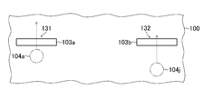
- FIG. 1A is a plan view showing a configuration of an optical circuit for alignment according to the first embodiment of the present invention.
- FIG. 1B is a flowchart for explaining the alignment method according to the first embodiment of the present invention.
- FIG. 2 is an explanatory diagram for explaining a state in which the arrangement direction of the plurality of optical fibers forming the fiber array is rotated by an angle ⁇ around the Z axis with respect to the Y axis.
- FIG. 3 shows a state in which the image does not rotate about the Z axis and ⁇ deg.
- FIG. 1A is a plan view showing a configuration of an optical circuit for alignment according to the first embodiment of the present invention.
- FIG. 1B is a flowchart for explaining the alignment method according to the first embodiment of the present invention.
- FIG. 2 is an explanatory diagram for explaining a state in which the arrangement direction of the plurality of optical fibers forming the fiber array is rotated by an angle ⁇ around the Z axis with respect to the Y
- FIG. 7 is a characteristic diagram showing the relationship between the amount of positional deviation ⁇ x in the X-axis direction and the rotation angle ⁇ between the first optical fiber 104a and the second optical fiber 104j while rotating only by 10 degrees.
- FIG. 4 is a characteristic diagram showing an intensity change (a) measured at the first light receiving point 131 and an intensity change (b) measured at the second light receiving point 132 due to the movement of the fiber array.
- FIG. 5 is a plan view showing a partial configuration of another optical circuit for alignment according to Embodiment 1 of the present invention.
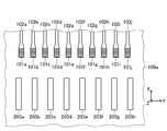
- FIG. 6A is a plan view showing a configuration of an optical circuit for alignment according to the second embodiment of the present invention.
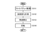
- FIG. 6B is a flowchart for explaining the alignment method according to the second embodiment of the present invention.
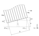
- FIG. 7 is an explanatory diagram for explaining a state in which the arrangement direction of the plurality of optical fibers forming the fiber array is rotated by an angle ⁇ 2 around the X axis with respect to the Y axis.
- FIG. 8 is a characteristic diagram showing changes in the deviation amounts ⁇ Y_a and ⁇ Y_j due to changes in ⁇ 2 when the distance H is 100 ⁇ m.
- FIG. 9 is an explanatory diagram for explaining a state in which the arrangement direction of the plurality of optical fibers forming the fiber array is rotated by an angle ⁇ 2 around the X axis with respect to the Y axis.
- FIG. 10 is an explanatory diagram for explaining the measurement of ⁇ Y2 using the plurality of optical sensors 203a to 203h.
- FIG. 11 is a characteristic diagram showing a light intensity profile H when the distance is H and a light intensity profile H2 when the distance is H2.
- FIG. 13 is a perspective view for explaining the alignment state of the fiber array 304 in which a plurality of SMFs are bundled and the plurality of grating couplers 301.
- FIG. 14 is a perspective view for explaining an alignment state between the fiber array 304 in which a plurality of SMFs are bundled and the plurality of grating couplers 301.
- This alignment optical circuit is first formed on a substrate 100 and is arranged on a plurality of grating couplers 101a, 101b, 101c, 101d, 101e, 101f, 101g, 101h, 101i and 101j.
- Optical waveguides 102a, 102b, 102c, 102d, 102e, 102f, 102g, 102h, 102i, 102j connected to the respective grating couplers 101a to 101j.
- the plurality of grating couplers 101a to 101j are arranged on the same straight line (on a line parallel to the Y axis) at equal intervals.
- the optical waveguides 102a to 102j are optically connected to an optical circuit (not shown) formed on the substrate 100.
- the direction in which the plurality of grating couplers 101a to 101j are arranged is the Y-axis direction.
- the alignment optical circuit is formed on the substrate 100 and has a first light receiving portion 131 and a second light receiving portion on a straight line along the arrangement direction (Y-axis direction) of the plurality of grating couplers 101a to 101j.
- An optical sensor 103 for measuring the light intensity is provided at 132.
- the optical sensor 103 includes the two first light receiving portions 131 and the second light receiving portions 132, and receives the light received extending along the arrangement direction (Y-axis direction) of the plurality of grating couplers 101a to 101j. Area.
- This optical circuit for centering is arranged around the Z-axis between the arraying direction of the plurality of optical fibers forming the fiber array to be centered and the arraying direction of the plurality of grating couplers 101a to 101j (Y-axis direction). Alignment of rotation deviation is performed.
- the Z axis is an axis perpendicular to the plane of the substrate 100.
- the first light receiving portion 131 and the second light receiving portion 132 where the optical sensor 103 measures the light intensity are arranged at any two intervals among the plurality of grating couplers 101a to 101j.
- the first light receiving location 131 and the second light receiving location 132 are, for example, at intervals between both ends of the plurality of grating couplers 101a to 101j.
- An object to be aligned by using this optical circuit for alignment is a fiber array in which a plurality of optical fibers are linearly arranged in one line. For example, a fiber array in which 10 optical fibers are arranged in a line.
- the optical sensor 103 can be composed of, for example, a well-known surface-illuminated photodiode (PD).
- PD surface-illuminated photodiode
- GePD having a light absorbing layer made of germanium
- SiPD having a light absorbing layer made of silicon, or the like
- the optical sensor 103 can receive the light emitted from each of the two first optical fibers 104a and the second optical fibers 104j to be aligned in the fiber array, the length of the light receiving region in the Y-axis direction. It must be long.
- the fiber array is composed of 10 optical fibers and the distance between adjacent optical fibers is 127 ⁇ m
- the distance between the first optical fiber 104a and the second optical fiber 104j at both ends of the fiber array is It becomes 1143 ⁇ m.
- the length of the light receiving region in the Y-axis direction is longer than 1143 ⁇ m.
- the fiber array is arranged with the light emission direction of each of the plurality of optical fibers of the fiber array facing the optical circuit for alignment.
- the fiber array is rotated by a predetermined angle around the Y axis, which is the direction in which a plurality of optical fibers are arranged.
- This angle is an incident/emission angle of light determined by the structure of the grating coupler, and in Non-Patent Document 1, for example, 20 deg. from the direction perpendicular to the substrate plane of the optical circuit for alignment.
- the tilt angle is within the range.
- the fiber array is moved in the direction (X-axis direction) perpendicular to the arrangement direction of the grating couplers 101a to 101j and passed (moved) over the optical sensor 103.
- the optical circuit for alignment is moved relative to the fiber array.
- the intensity change of each of the first light emitted from the first optical fiber 104a and the second light emitted from the second optical fiber 104j is detected by the first light receiving portion 131 and the second light receiving portion 132 of the optical sensor 103.
- the photocurrents flowing through the first light receiving portion 131 and the second light receiving portion 132 of the optical sensor 103 are simultaneously measured.
- the amount of displacement of the fiber array in the ⁇ z direction is small, it is possible that two lights are simultaneously incident on the PD and the photocurrents generated by the two lights cannot be separated. In this case, the two currents are not measured at the same time, but the light is emitted from one fiber, and then the light is emitted from the other fiber to measure the photocurrent. It can be measured separately.
- the arrangement direction of the plurality of optical fibers forming the fiber array is around the Z axis with respect to the arrangement direction (Y axis) of the plurality of grating couplers 101a to 101j.
- the angle ⁇ it is difficult to align all the optical fibers and each of the grating couplers 101a to 101j at the same time.
- the optical connection has a large coupling loss. When the coupling loss is large, the port dependence of the insertion loss of the optical signal with respect to the optical circuit also occurs.
- the fiber array is composed of 10 optical fibers
- ⁇ deg The positional relationship between the first optical fiber 104a and the second optical fiber 104j at both ends of the fiber array when only rotating is as shown in FIG.
- the distance D between the first optical fiber 104 a and the second optical fiber 104 j is 1143 ⁇ m.
- the state of not rotating around the Z axis and ⁇ deg.
- the relationship between the positional deviation amount ⁇ x in the X-axis direction between the first optical fiber 104a and the second optical fiber 104j and the rotation angle ⁇ is as shown in FIG. .. If ⁇ is 0, the positional deviation amount ⁇ x in the X-axis direction between the first optical fiber 104a and the second optical fiber 104j is 0. On the other hand, for example, when ⁇ is 0.5 deg. It can be seen that ⁇ X becomes about 10 ⁇ m, and the positional deviation of each of the first optical fiber 104a and the second optical fiber 104j from the corresponding grating coupler becomes 5 ⁇ m. Considering that the core diameter of the optical fiber is about 10 ⁇ m, the above-mentioned numerical values lead to a fatal misalignment.
- the positional deviation due to the rotation of the fiber array around the Z axis is obtained by the above-described first step S101 to third step S103.
- the intensity change (a) is measured at the first light receiving point 131 and the intensity change (b) is measured at the second light receiving point 132 as shown in FIG. To be done.
- the angle ⁇ is obtained from the difference between the intensity change (a) and the intensity change (b).
- the shift between the peak position of intensity change (a) and the peak position of intensity change (b) corresponds to ⁇ X.
- the adjustment is performed.
- the alignment direction is performed (rotation) by rotating the arrangement direction of the plurality of optical fibers of the fiber array by the angle obtained in the third step.
- the fiber array which has been aligned by adjusting the angle around the Z-axis, is moved in parallel on the plane of the substrate 100 while maintaining the adjusted angle, and the plurality of grating couplers 101a to 101j are moved. It is placed at the optical connection position with.
- one optical sensor 103 having the light receiving region extending from the first light receiving portion 131 to the second light receiving portion 132 and extending in the Y-axis direction is used, but as shown in FIG. You may make it use the 1st optical sensor 103a and the 2nd optical sensor 103b formed on 100.
- the first optical sensor 103a and the second optical sensor 103b are formed in each of the first light receiving portion 131 and the second light receiving portion 132.
- the optical sensor 103 (the first optical sensor 103a and the second optical sensor 103b) may be arranged at any place on the substrate 100.
- the difference in the intensity of the first light emitted from the first optical fiber and the difference in the intensity of the second light emitted from the second optical fiber is determined by the difference in the peak positions from the plane of the alignment optical circuit.
- the angle formed by the arrangement direction (Y-axis direction) of the plurality of grating couplers and the arrangement direction of the plurality of optical fibers is determined in a plane parallel to the above, but the present invention is not limited to this.
- a difference in position (deviation amount) having the same intensity is used for alignment.
- the angle formed by the arrangement direction of the plurality of grating couplers (Y-axis direction) and the arrangement direction of the plurality of optical fibers can be determined within a plane parallel to the plane of the optical circuit.
- the optical sensor 103 has a large width (length in the X-axis direction) and the fiber array is moved in the X-axis direction, one peak position of intensity change may not appear.
- the above angle is obtained from the difference in the slope portions (positions having the same strength) that change in the same state in the strength change.
- the width of the optical sensor 103 is calculated as follows. As shown in (4), it is desirable that the angle be set to a predetermined size in consideration of the angle to be detected and the spot size of light emitted from the optical fiber.
- the width of the optical sensor 103 is preferably 30 ⁇ m or less. The limit value of the minimum width of the optical sensor 103 is determined by the manufacturing restrictions of the optical sensor 103.
- the optical sensor that measures the light intensity at two points on the straight line extending along the arrangement direction on the substrate on which the plurality of grating couplers are formed.
- This alignment optical circuit is first formed on a substrate 100a and has a plurality of linearly arranged grating couplers 101a to 101j and a plurality of optical waveguides 102a connected to each of the plurality of grating couplers 101a to 101j. .About.102j. These are the same as those in the first embodiment described above.
- this optical circuit for alignment is formed on the substrate 100a, and the plurality of optical sensors 203a, 203b, 203c, which are arranged along the arrangement direction (Y-axis direction) of the plurality of grating couplers 101a to 101j, 203d, 203e, 203f, 203g, 203h are provided.
- Each of the optical sensors 203a to 203h includes a light receiving region extending in a direction (X-axis direction) orthogonal to the arrangement direction of the plurality of grating couplers 101a to 101j. The location where each of the optical sensors 203a to 203h is arranged becomes a light receiving location.
- the alignment optical circuit performs alignment regarding rotation deviation around the X axis in the arrangement direction of the plurality of optical fibers forming the fiber array to be aligned. In other words, the alignment optical circuit determines the rotation deviation angle around the X axis between the arrangement direction of the plurality of optical fibers forming the fiber array to be aligned and the plane of the substrate 100a.
- the subject of the centering using the centering optical circuit of the second embodiment is a fiber array formed by arranging a plurality of optical fibers in a straight line.
- a fiber array in which 10 optical fibers are arranged in a line is arranged.
- Each of the optical sensors 203a to 203h can be composed of, for example, a well-known surface incidence type PD.
- a well-known surface incidence type PD As the surface-incidence PD, GePD having a light absorbing layer made of germanium, SiPD having a light absorbing layer made of silicon, or the like can be used.
- the length of the light-receiving region in the X-axis direction is emitted from each of the two first optical fibers 104a and the second optical fiber 104j to be aligned in the fiber array. It must be long enough to receive light.
- the fiber array to be aligned is determined by the design of the grating from the direction perpendicular to the substrate plane of the optical circuit for alignment as described above. It is rotated around the Y-axis by the angle of.
- the angle described above is set to 20 deg. It is within.
- the rotation angle around the Y axis is ⁇ Y
- the length of the above-described light receiving region in the X axis direction is determined by the relationship between ⁇ Y and the ascending amount of the fiber array described later, and the X axis of the optical axis of the optical fiber. The length needs to take into consideration the shift amount in the direction and the spot size of the light. This point will be described later.
- the fiber array is arranged with the light emitting direction of each of the plurality of optical fibers of the fiber array facing the optical circuit for alignment.
- the fiber array is rotated by a predetermined angle around the Y axis, which is the direction in which a plurality of optical fibers are arranged.
- the fiber array is moved from the plane of the optical circuit for alignment. Move it away.
- an optical circuit for alignment (which may be a fiber array) is fixed on an electric stage having a stepping motor, and the electric stage is moved (moved up and down) to relatively align the fiber array with respect to the fiber array.
- each of the first light emitted from the first optical fiber 104a and the second light emitted from the second optical fiber 104j passes over the plurality of optical sensors 203a to 203h, and the first light and The change in the intensity of each of the second lights is measured by the plurality of photosensors 203a to 203h.
- the arrangement direction (Y-axis) of the plurality of grating couplers 101a to 101j is determined.
- the angle ⁇ 2 between the plane of the substrate 100 and the arrangement direction of the plurality of optical fibers in the fiber array about the axis (X axis) perpendicular to () is calculated (angle calculation).
- the irradiation position of the light emitted from the first optical fiber 104a on the substrate shifts by ⁇ Y_a depending on whether the light is rotated or not.
- the irradiation position of the light emitted from the second optical fiber 104j on the substrate deviates by ⁇ Y_j depending on whether it is rotated or not. It should be noted that these shift amounts are assumed when the fiber array 104 and the substrate surface of the optical circuit for alignment are separated by a distance H.
- the deviation amounts ⁇ Y_a and ⁇ Y_j described above change as shown in FIG. 8 when ⁇ 2 changes.
- the result of FIG. 8 is obtained as a result of calculation.
- the deviation amounts ⁇ Y_a and ⁇ Y_j increase as ⁇ 2 increases. Further, as ⁇ 2 increases, the difference between the shift amount ⁇ Y_a and the shift amount ⁇ Y_j increases.
- the deviation amounts ⁇ Y_a and ⁇ Y_j described above also change depending on the change in the distance between the fiber array 104 and the substrate surface of the optical circuit for alignment, even if ⁇ 2 is constant. As shown in FIG. 9, when the distance H between the fiber array 104 and the substrate surface of the optical circuit for alignment is changed to the distance H2, first, the irradiation position of the light emitted from the first optical fiber 104a on the substrate is shifted. The amount increases by ⁇ Y2 from ⁇ Y_a.
- ⁇ Y2 generated by moving the fiber array 104 in a direction away from the plane of the optical circuit for alignment is determined by the above-described first step S111 to third step S113. As shown in FIG. 10, ⁇ Y2 is measured using a plurality of stripe-shaped photosensors 203a to 203h in which the shape of each light receiving region in plan view extends in the X-axis direction.
- the plurality of optical sensors 203a to 203h shift the optical axis of the optical fiber in the X-axis direction, which is determined by the relationship between the length of each light-receiving region in the X-axis direction in the direction of ⁇ Y and the amount of elevation (H2-H) of the fiber array.
- the length is set in consideration of the amount and the spot size of light.
- the arrangement interval of the plurality of optical sensors 203a to 203h can be determined by the desired ⁇ 2 and the amount of increase from the distance H to the distance H2.
- the length in the Y-axis direction of each light receiving region of the plurality of optical sensors 203a to 203h needs to be equal to or less than the above-mentioned arrangement interval.
- ⁇ Y2 is calculated by comparing the intensity profiles of the generated light before and after the movement.
- the light intensity profile H when the distance between the fiber array and the substrate surface of the optical circuit for alignment is H
- the distance between the fiber array and the substrate surface of the optical circuit for alignment is
- the horizontal axis represents the optical sensors 203a to 203h
- the optical circuit for centering is performed.
- the alignment direction is performed (rotation) by rotating the arrangement direction of the plurality of optical fibers of the fiber array by the angle obtained in the third step.
- the fiber array which has been aligned by adjusting the angle around the X-axis, is moved in parallel on the plane of the substrate 100 while maintaining the adjusted angle, and the plurality of grating couplers 101a to 101j are moved. It is placed at the optical connection position with.
- the case where eight optical sensors 203a to 203h are used has been described as an example, but the number of optical sensors may be two or more. Further, by using a larger number of optical sensors, there is an advantage that ⁇ Y2 can be obtained even when ⁇ Y2>the arrangement interval of the optical sensors.
- the plurality of optical sensors arranged along the arrangement direction of the plurality of grating couplers are provided on the substrate on which the plurality of grating couplers are formed. Therefore, the alignment for obtaining the optical connection between the plurality of optical fibers of the fiber array in which the plurality of optical fibers are bundled and the corresponding grating coupler can be easily performed.
- a plurality of light receiving portions are provided on the substrate on which a plurality of grating couplers are formed, a plurality of fiber arrays in which a plurality of optical fibers are bundled are provided.
- the alignment for obtaining the optical connection between the optical fiber and the corresponding grating coupler can be easily performed.
Landscapes
- Physics & Mathematics (AREA)
- General Physics & Mathematics (AREA)
- Optics & Photonics (AREA)
- Engineering & Computer Science (AREA)
- Microelectronics & Electronic Packaging (AREA)
- Optical Couplings Of Light Guides (AREA)
Abstract
基板(100)の上に形成されて、直線上に配列する複数のグレーティングカプラ(101a),(101b),(101c),(101d),(101e),(101f),(101g),(101h),(101i),(101j)と、複数のグレーティングカプラ(101a)~(101j)の各々に接続された複数の光導波路(102a)~(102j)とを備える。また、基板(100)の上に形成されて、複数のグレーティングカプラ(101a)~(101j)の配列方向(Y軸方向)に沿った直線上の第1受光箇所(131),第2受光箇所(132)で光強度を測定する光センサ(103)を備える。
Description
本発明は、調芯用光回路および調芯方法に関し、より詳しくは、グレーティングカプラと光ファイバとの光接続に用いる調芯用光回路および調芯方法に関する。
シリコン光回路と光ファイバとの光学的な接続(光接続)には、これまで、導波路端面と光ファイバの光接続の効率を向上させるために、スポットサイズコンバータや先球ファイバなどが使用されてきた。近年、微細加工の技術の進展により、シリコン導波路に、幅が数百nmの溝からなるグレーティングを設け、光導波路から基板表面に対して上方、下方に光を放射させるグレーティングカプラとして機能させ、光ファイバと光接続させる例が多くみられるようになった。
例えば、シリコンフォトニクスにおいて、光ファイバとの光接続にグレーティングカプラを用いる技術が提案されている(非特許文献1参照)。この技術では、グレーティングカプラからの光の上面への光の出射角度は、非特許文献1の7870頁に記載されている式(1)を満たす角度となり、基板に対して垂直な方向から20deg.以内の傾き角とされている。グレーティングカプラを用いる利点は,基板表面に対して上方から光を入出力できることにある。このため、グレーティングカプラを用いた光接続の技術は、光回路をウエハに複数形成している状態での各光回路の検査などに適している。
グレーティングカプラに光を結合させる場合には、シングルモードファイバ(SMF)やファイバアレイなどが用いられる。例えば、光回路では、光回路の光入力端に入力用グレーティングカプラを設け、光回路の光出力端に出力用グレーティングカプラを設け、光回路の検査に利用している。例えば、入力用SMFから出射される光を入力用グレーティングカプラに光接続させる。一方で、出力用グレーティングカプラより出射される光を出力用SMFに光接続させて取り出し、光回路の検査に用いる。
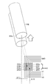
この場合、入力用SMFと入力用グレーティングカプラとの調芯と、出力用SMFと出力用グレーティングカプラとの調芯とが必要となる。これらの調芯を1つの調芯装置で実施するために、図13に示すように、複数のSMFが束ねられたファイバアレイ304を用い、また、検査対象の光回路300の光導波路302に接続されている複数のグレーティングカプラ301を、ファイバアレイ304のSMFの配列ピッチで配置することが考えられる。
例えば、ファイバアレイ304の中の一端のSMFと、対応するグレーティングカプラ301を入力用とし、ファイバアレイ304の中の他端のSMFと、対応するグレーティングカプラ301を出力用として用いれば、1つの光学調芯系(装置)で、入力用と出力用の両者の調芯を実施することができる。また、上述した構成とすることで、各グレーティングカプラ301を用いた、光回路300の複数のグレーティングカプラにおける、光結合の状態の測定も可能となる。
C. Li et al., "CMOS-compatible high efficiency double-etched apodized waveguide grating coupler", Optics Express, vol. 21, no. 7, pp. 7868-7874, 2013.
しかしながら、上述したようにファイバアレイ304を用いる場合、複数のSMFと複数のグレーティングカプラ301と間の調芯を、同時に行うことになる。ファイバアレイ304を用いた場合は、図14に示すように、光回路300の平面の法線方向であるZ軸周り、およびファイバアレイの複数のSMFの配列方向に垂直な方向であるX軸周りに、ファイバアレイ304が回転していると(ずれていると)、複数のグレーティングカプラ301と複数のSMFとを、同時に、最適な状態で光接続させることが困難である。
本発明は、以上のような問題点を解消するためになされたものであり、複数の光ファイバが束ねられたファイバアレイの複数の光ファイバと対応するグレーティングカプラとの光学的な接続を得るための調芯が、容易に実施できるようにすることを目的とする。
本発明に係る調芯用光回路は、基板の上に形成されて、直線上に配列する複数のグレーティングカプラと、複数のグレーティングカプラの各々に接続された複数の光導波路と、基板の上に形成されて、複数のグレーティングカプラの配列方向に沿った直線上の2つの受光箇所で光強度を測定する光センサとを備え、2つの受光箇所の間隔は、複数のグレーティングカプラの中のいずれか2つの間隔とされている。
上記調芯用光回路の一構成例において、光センサは、2つの受光箇所を含んで配列方向に沿って延在する受光領域を備える。
上記調芯用光回路の一構成例において、光センサは、2つの受光箇所の各々に形成されている。
上記調芯用光回路の一構成例において、2つの受光箇所は、複数のグレーティングカプラの両端の間隔とされている。
本発明に係る調芯用光回路は、基板の上に形成されて、直線上に配列する複数のグレーティングカプラと、複数のグレーティングカプラの各々に接続された複数の光導波路と、基板の上に形成されて、複数のグレーティングカプラの配列方向に沿って配列された複数の光センサとを備える。
本発明に係る調芯方法は、基板の上に形成されて、直線上に配列する複数のグレーティングカプラと、複数のグレーティングカプラの各々に接続された複数の光導波路と、基板の上に形成されて、複数のグレーティングカプラの配列方向に沿った直線上の2つの受光箇所で光強度を測定する光センサとを備える調芯用光回路と、複数のグレーティングカプラのいずれか2つの第1グレーティングカプラおよび第2グレーティングカプラと、複数の光ファイバが直線上に1列に配列して形成されたファイバアレイのいずれか2つの第1光ファイバおよび第2光ファイバの各々とを調芯する調芯方法であって、複数の光ファイバの各々の光出射方向を調芯用光回路の側に向けてファイバアレイを配置する第1工程と、第1光ファイバおよび第2光ファイバより調芯用光回路の側に光を出射させている状態で、調芯用光回路の平面に平行な平面内で、ファイバアレイを、グレーティングカプラの配列方向に垂直な方向に移動させて光センサの上を通過させ、第1光ファイバから出射される第1光および第2光ファイバから出射される第2光の各々の強度変化を、2つの受光箇所で計測する第2工程と、光センサにより計測した第1光の強度変化と第2光の強度変化との違いから、調芯用光回路の平面に平行な平面内で、複数のグレーティングカプラの配列方向と、複数の光ファイバの配列方向とのなす角度を求める第3工程と調芯用光回路の平面に平行な平面内で、複数の光ファイバの配列方向を、第3工程で求めた角度回転させることで調芯を実施する第4工程とを備える。
本発明に係る調芯方法は、基板の上に形成されて、直線上に配列する複数のグレーティングカプラと、複数のグレーティングカプラの各々に接続された複数の光導波路と、複数のグレーティングカプラの配列方向に沿って配列された複数の光センサとを備える調芯用光回路と、複数のグレーティングカプラのいずれか2つの第1グレーティングカプラおよび第2グレーティングカプラと、複数の光ファイバが直線上に1列に配列して形成されたファイバアレイのいずれか2つの第1光ファイバおよび第2光ファイバの各々とを調芯する調芯方法であって、複数の光ファイバの各々より出射される光が、複数の光センサのいずれかに受光される状態にファイバアレイを配置する第1工程と、第1光ファイバおよび第2光ファイバより調芯用光回路の側に光を出射させている状態で、ファイバアレイを、調芯用光回路の平面より離れる方向に移動させ、第1光ファイバから出射される第1光および第2光ファイバから出射される第2光の各々の強度変化を、複数の光センサにより計測する第2工程と、複数の光センサにより計測した第1光の強度変化と第2光の強度変化との違いから、複数のグレーティングカプラの配列方向に垂直な軸を中心とした、基板の平面と複数の光ファイバの配列方向とのなす角度を求める第3工程と、軸を中心として複数の光ファイバの配列方向を、第3工程で求めた角度回転させることで調芯を実施する第4工程とを備える。
以上説明したように、本発明によれば、複数のグレーティングカプラが形成されている基板の上に複数の受光箇所を設けるようにしたので、複数の光ファイバが束ねられたファイバアレイの複数の光ファイバと対応するグレーティングカプラとの光学的な接続を得るための調芯が、容易に実施できるようになる。
以下、本発明の実施の形態に係る調芯用光回路および調芯方法について説明する。
[実施の形態1]
はじめに、本発明の実施の形態1に係る調芯用光回路について、図1Aを参照して説明する。この調芯用光回路は、まず、基板100の上に形成されて、直線上に配列する複数のグレーティングカプラ101a,101b,101c,101d,101e,101f,101g,101h,101i,101jと、複数のグレーティングカプラ101a~101jの各々に接続された複数の光導波路102a,102b,102c,102d,102e,102f,102g,102h,102i,102jとを備える。複数のグレーティングカプラ101a~101jは、同一の直線上(Y軸に平行な線上)に、等しい間隔で配列されている。また、光導波路102a~102jは、基板100の上に形成されている図示しない光回路に光接続している。なお、複数のグレーティングカプラ101a~101jが配列されている方向が、Y軸の方向である。
はじめに、本発明の実施の形態1に係る調芯用光回路について、図1Aを参照して説明する。この調芯用光回路は、まず、基板100の上に形成されて、直線上に配列する複数のグレーティングカプラ101a,101b,101c,101d,101e,101f,101g,101h,101i,101jと、複数のグレーティングカプラ101a~101jの各々に接続された複数の光導波路102a,102b,102c,102d,102e,102f,102g,102h,102i,102jとを備える。複数のグレーティングカプラ101a~101jは、同一の直線上(Y軸に平行な線上)に、等しい間隔で配列されている。また、光導波路102a~102jは、基板100の上に形成されている図示しない光回路に光接続している。なお、複数のグレーティングカプラ101a~101jが配列されている方向が、Y軸の方向である。
また、この調芯用光回路は、基板100の上に形成されて、複数のグレーティングカプラ101a~101jの配列方向(Y軸方向)に沿った直線上の第1受光箇所131,第2受光箇所132で光強度を測定する光センサ103を備える。実施の形態1において、光センサ103は、2つの第1受光箇所131,第2受光箇所132を含んで、複数のグレーティングカプラ101a~101jの配列方向(Y軸方向)に沿って延在する受光領域を備える。
この調芯用光回路は、調芯対象のファイバアレイを構成している複数の光ファイバの配列方向と、複数のグレーティングカプラ101a~101jの配列方向(Y軸方向)との、Z軸周りの回転ずれに関する調芯を実施する。つまり、この調芯用光回路により、調芯対象のファイバアレイを構成している複数の光ファイバの配列方向と、複数のグレーティングカプラ101a~101jの配列方向(Y軸方向)との、Z軸周りの回転ずれ角を求める。なお、Z軸は、基板100の平面に垂直な軸である。
光センサ103が光強度測定を実施する第1受光箇所131,第2受光箇所132は、複数のグレーティングカプラ101a~101jの中のいずれか2つの間隔とされている。第1受光箇所131,第2受光箇所132は、例えば、複数のグレーティングカプラ101a~101jの両端の間隔とされている。なお、この調芯用光回路を用いて調芯を実施する対象は、複数の光ファイバが直線上に1列に配列して形成されたファイバアレイである。例えば、10個の光ファイバが、一列に配列したファイバアレイである。
光センサ103は、例えば、よく知られた面入射型のフォトダイオード(Photo Diode:PD)から構成できる。面入射型のPDは、ゲルマニウムからなる光吸収層を備えるGePDや、シリコンからなる光吸収層を備えるSiPDなどを用いることができる。光センサ103は、受光領域のY軸方向の長さが、ファイバアレイの中の、調芯対象となる2つの第1光ファイバ104a,第2光ファイバ104jの各々から出射される光が受光できる長さとなっていることが必要である。例えば、ファイバアレイが10本の光ファイバから構成され、隣り合う光ファイバの間隔が、127μmとされている場合、ファイバアレイの両端の第1光ファイバ104aと第2光ファイバ104jとの間隔は、1143μmとなる。この場合、光センサ103は、受光領域のY軸方向の長さは、1143μmより長くする。
次に、実施の形態1に係る調芯方法について、図1Bのフローチャートを用いて説明する。まず、第1工程S101で、ファイバアレイの複数の光ファイバの各々の光出射方向を調芯用光回路の側に向けてファイバアレイを配置する。なお、ファイバアレイは、複数の光ファイバが配列されている方向であるY軸の周りに、所定角度回転させている。この角度は、グレーティングカプラの構造によって決まる光の入出射角であり、例えば、非特許文献1では、調芯用光回路の基板平面に対して垂直な方向から20deg.以内の傾き角とされている。
次に、第2工程S102で、第1光ファイバ104aおよび第2光ファイバ104jより調芯用光回路の側に光を出射させている状態で、調芯用光回路の平面に平行な平面内で、ファイバアレイを、グレーティングカプラ101a~101jの配列方向に垂直な方向(X軸方向)に移動させて光センサ103の上を通過(移動)させる。
例えば、ステッピングモータなどを有する電動ステージの上に調芯用光回路(ファイバアレイでも良い)を固定し、電動ステージを移動させることで、ファイバアレイに対して相対的に調芯用光回路を移動させることで、上述したファイバアレイの通過を実施することができる。これにより、第1光ファイバ104aから出射される第1光および第2光ファイバ104jから出射される第2光の各々の強度変化を、光センサ103の第1受光箇所131および第2受光箇所132の各々で計測する(強度変化計測)。例えば、光センサ103の第1受光箇所131および第2受光箇所132に流れる各々の光電流を同時に計測する。ファイバアレイのθz方向のずれ量が小さい場合、2つの光が同時にPDに入射される状態となり、2つの光によって生じる光電流が分離できないことが起こり得る。この場合は、2つの光を同時測定せず、1方のファイバから光を出した状態で測定し、この後、もう1方のファイバから光を出した状態で測定することで、光電流を分離して測定することができる。
次に、第3工程S103で、光センサ103により計測した第1光の強度変化と第2光の強度変化との違いから、調芯用光回路の基板平面に平行な平面内で、複数のグレーティングカプラ101a~101jの配列方向(Y軸方向)と、ファイバアレイにおける複数の光ファイバの配列方向とのなす角度θを求める(角度算出)。
例えば、図2に示すように、ファイバアレイを構成している複数の光ファイバの配列方向が、複数のグレーティングカプラ101a~101jが配列されている方向(Y軸)に対して、Z軸周りに角度θ回転している状態では、全ての光ファイバとグレーティングカプラ101a~101jとの各々を、同時に調芯することが困難である。例えば、ファイバアレイの中心付近の光ファイバと、これに対するグレーティングカプラとの光接続が最適になるように調芯しても、ファイバアレイの中心から離れている光ファイバと、これに対するグレーティングカプラとの光接続は、結合損失が大きくなる。結合損失が大きい状態では、光回路に対する光信号の挿入損失のポート依存性も生じてしまう。
例えば、ファイバアレイが10本の光ファイバから構成されている場合、ファイバアレイの中心を回転中心として、Z軸周りにθdeg.だけ回転しているときの、ファイバアレイの両端の第1光ファイバ104aと第2光ファイバ104jとの位置関係は、図2に示す状態となる。ファイバアレイの隣り合う光ファイバの間隔を、典型的な127μmとすると、第1光ファイバ104aと第2光ファイバ104jとの間隔Dは、1143μmとなる。
この場合、Z軸周りに回転していない状態と、Z軸周りにθdeg.だけ回転している状態との間で、第1光ファイバ104aと第2光ファイバ104jとの間のX軸方向の位置ずれ量Δxと回転角度θとの関係は、図3に示すものとなる。θが0なら、第1光ファイバ104aと第2光ファイバ104jとの間のX軸方向の位置ずれ量Δxは、0となる。これに対し、例えば,θが0.5deg.となるだけで,ΔXは約10μmとなり、第1光ファイバ104aおよび第2光ファイバ104jの各々の、対応するグレーティングカプラからの位置ずれは、5μmとなることが分かる。光ファイバのコア径が10μmで程度あることを考慮すると、上述した数値は、致命的な位置ずれにつながる。
この、ファイバアレイのZ軸周りの回転による位置ずれを、前述した第1工程S101~第3工程S103により求める。第2工程S102の強度変化計測により、図4に示すように、ファイバアレイの移動により第1受光箇所131で強度変化(a)が計測され、第2受光箇所132で強度変化(b)が計測される。この強度変化(a)と強度変化(b)との違いから、角度θが求められる。例えば、強度変化(a)のピーク位置と強度変化(b)のピーク位置のずれが、ΔXに対応する。図4に示す例では、ΔX=6μmとなる。ΔX=6μmであるなら、図2,図3を用いて説明したΔXとθとの関係より、θ=0.3deg.であることが分かる。
以上のように、複数のグレーティングカプラ101a~101jの配列方向(Y軸方向)と、ファイバアレイにおける複数の光ファイバの配列方向とのなす角度θが求められた後、第4工程S104で、調芯用光回路の基板平面に平行な平面内で、ファイバアレイの複数の光ファイバの配列方向を、第3工程で求めた角度回転させることで調芯を実施する(回転)。また、上述したように、Z軸周りの角度調整による調芯を実施したファイバアレイを、調整した角度を維持した状態で、基板100の平面上を平行に移動させ、複数のグレーティングカプラ101a~101jとの光接続位置に配置する。
ところで、上述では、第1受光箇所131から第2受光箇所132を含んでY軸方向に延在する受光領域を備える1つの光センサ103を用いるようにしたが、図5に示すように、基板100の上に形成された、第1光センサ103aおよび第2光センサ103bを用いるようにしてもよい。第1光センサ103aおよび第2光センサ103bは、第1受光箇所131および第2受光箇所132の各々に形成されている。光センサ103(第1光センサ103a、第2光センサ103b)は、基板100の上の任意の場所に配置されていればよい。
また、上述では、第1光ファイバから出射される第1光および第2光ファイバから出射される第2光の各々の強度変化の違いとして、ピーク位置の違いより、調芯用光回路の平面に平行な平面内で、複数のグレーティングカプラの配列方向(Y軸方向)と、複数の光ファイバの配列方向とのなす角度を求めたが、これに限るものではない。例えば、第1光ファイバから出射される第1光および第2光ファイバから出射される第2光の各々の強度変化の違いとして、同じ強度となる位置の違い(ずれ量)より、調芯用光回路の平面に平行な平面内で、複数のグレーティングカプラの配列方向(Y軸方向)と、複数の光ファイバの配列方向とのなす角度を求めることができる。
例えば、光センサ103の幅(X軸方向の長さ)が大きく、ファイバアレイを、X軸方向に移動させる範囲では、一方の強度変化のピーク位置が出現しない場合がある。このような場合、強度変化の中で、同一の状態で変化しているスロープの箇所(同じ強度となる位置)の違いより、上記角度を求める。
なお、第1光ファイバから出射される第1光および第2光ファイバから出射される第2光の各々の強度変化の違いとして、ピーク位置を用いるためには、光センサ103の幅を、以下に示すように、検出したい角度と光ファイバから出射される光のスポットサイズを考慮した所定の大きさに収めることが望ましい。
例えば、ファイバアレイが10本の光ファイバから構成され、隣り合う光ファイバの間隔が、127μmとされ、スポットサイズが20μmの場合、θ=0.5deg.の角度ずれを検出したい場合、光センサ103の幅は、30μm以下とすることが望ましい。なお、光センサ103の最小幅の限界値は、光センサ103の製造上の制約で決定される。
以上に説明したように、実施の形態1によれば、複数のグレーティングカプラが形成されている基板の上に、配列方向に沿って延在する直線上の2箇所で光強度を測定する光センサを備えるようにしたので、複数の光ファイバが束ねられたファイバアレイの複数の光ファイバと対応するグレーティングカプラとの光学的な接続を得るための調芯が、容易に実施できるようになる。
[実施の形態2]
次に、本発明の実施の形態2に係る調芯用光回路について、図6Aを参照して説明する。この調芯用光回路は、まず、基板100aの上に形成され、直線上に配列する複数のグレーティングカプラ101a~101jと、複数のグレーティングカプラ101a~101jの各々に接続された複数の光導波路102a~102jとを備える。これらは、前述した実施の形態1と同様である。
次に、本発明の実施の形態2に係る調芯用光回路について、図6Aを参照して説明する。この調芯用光回路は、まず、基板100aの上に形成され、直線上に配列する複数のグレーティングカプラ101a~101jと、複数のグレーティングカプラ101a~101jの各々に接続された複数の光導波路102a~102jとを備える。これらは、前述した実施の形態1と同様である。
また、この調芯用光回路は、基板100aの上に形成されて、複数のグレーティングカプラ101a~101jの配列方向(Y軸方向)に沿って配列された複数の光センサ203a,203b,203c,203d,203e,203f,203g,203hを備える。光センサ203a~203hの各々は、複数のグレーティングカプラ101a~101jの配列方向に直交する方向(X軸方向)延在する受光領域を備える。光センサ203a~203hの各々の配置箇所が、受光箇所となる。この調芯用光回路は、調芯対象のファイバアレイを構成している複数の光ファイバの配列方向の、X軸周りの回転ずれに関する調芯を実施する。つまり、この調芯用光回路により、調芯対象のファイバアレイを構成している複数の光ファイバの配列方向と、基板100aの平面との間の、X軸周りの回転ずれ角を求める。
実施の形態2の調芯用光回路を用いて調芯を実施する対象は、複数の光ファイバが直線上に1列に配列して形成されたファイバアレイである。例えば、10個の光ファイバが、一列に配列したファイバアレイである。
光センサ203a~203hの各々は、例えば、よく知られた面入射型のPDから構成できる。面入射型のPDは、ゲルマニウムからなる光吸収層を備えるGePDや、シリコンからなる光吸収層を備えるSiPDなどを用いることができる。
光センサ203a~203hの各々は、受光領域のX軸方向の長さが、ファイバアレイの中の、調芯対象となる2つの第1光ファイバ104a,第2光ファイバ104jの各々から出射される光が受光できる長さとなっていることが必要である。
調芯の対象となるファイバアレイは、複数のグレーティングカプラ101a~101jとの光接続において、前述したように、調芯用光回路の基板平面に対して垂直な方向から、グレーティングの設計で決まる所定の角度だけY軸の周りに回転させて配置する。例えば、非特許文献1では、上述した角度を20deg.以内としている。このY軸の周りの回転角度を、θYとすると、上述した受光領域のX軸方向の長さは、θYと、後述するファイバアレイの上昇量の関係から決まる、光ファイバの光軸のX軸方向のシフト量と光のスポットサイズとを考慮に入れた長さが必要である。この点については、後述する。
次に、実施の形態2に係る調芯方法について、図6Bのフローチャートを用いて説明する。まず、第1工程S111で、ファイバアレイの複数の光ファイバの各々の光出射方向を調芯用光回路の側に向けてファイバアレイを配置する。なお、前述同様に、ファイバアレイは、複数の光ファイバが配列されている方向であるY軸の周りに、所定角度回転させておく。
次に、第2工程S112で、第1光ファイバ104aおよび第2光ファイバ104jより調芯用光回路の側に光を出射させている状態で、ファイバアレイを、調芯用光回路の平面より離れる方向に移動させる。例えば、ステッピングモータなどを有する電動ステージの上に調芯用光回路(ファイバアレイでも良い)を固定し、電動ステージを移動(上下動)させることで、ファイバアレイに対して相対的に調芯用光回路を移動させることで、上述したファイバアレイの移動が実施できる。
この移動により、第1光ファイバ104aから出射される第1光および第2光ファイバ104jから出射される第2光の各々を、複数の光センサ203a~203hの上を通過させ、第1光および第2光の各々の強度変化を、複数の光センサ203a~203hにより計測する。
次に、第3工程S113で、複数の光センサ203a~203hにより計測した第1光の強度変化と第2光の強度変化との違いから、複数のグレーティングカプラ101a~101jの配列方向(Y軸)に垂直な軸(X軸)を中心とした、基板100の平面と、ファイバアレイの複数の光ファイバの配列方向とのなす角度θ2を求める(角度算出)。
例えば、図7に示すように、ファイバアレイ104を構成している複数の光ファイバの配列方向が、基板平面に対してX軸周りに角度θ2回転している状態では、全ての光ファイバとグレーティングカプラ101a~101jとの各々を、同時に調芯することが困難である。
ここで、ファイバアレイ104の複数の光ファイバの配列方向が、基板平面に対して平行ではなく、X軸周りに回転している場合と、回転していなく両者が互いに平行な場合(θ2=0deg.)と比較する。まず、第1光ファイバ104aから出射された光の基板上の照射位置は、回転している場合と回転していない場合とで、ΔY_aずれる。また、第2光ファイバ104jから出射された光の基板上の照射位置は、回転している場合と回転していない場合とで、ΔY_jずれる。なお、これらのずれ量は、ファイバアレイ104と調芯用光回路の基板面とが、距離H離れている場合とする。
上述した距離Hを100μmとした場合に、上述したずれ量ΔY_aと、ΔY_jは、θ2が変化すると図8に示すように変化する。なお、図8の結果は、計算の結果得られたものである。θ2が大きくなるにつれ、ずれ量ΔY_aと、ΔY_jは大きくなる。また、θ2が大きくなるにつれ、ずれ量ΔY_aと、ずれ量ΔY_jとの差が大きくなる。
上述したずれ量ΔY_aと、ΔY_jは、θ2が一定であっても、ファイバアレイ104と調芯用光回路の基板面との距離の変化によっても変化する。図9に示すように、ファイバアレイ104と調芯用光回路の基板面との距離Hを距離H2に変更すると、まず、第1光ファイバ104aから出射された光の基板上の照射位置のずれ量は、ΔY_aからΔY2増加する。また、ファイバアレイ104と調芯用光回路の基板面との距離Hを距離H2に変更すると、第2光ファイバ104jから出射された光の基板上の照射位置のずれ量は、ΔY_jからΔY2増加する。距離Hを距離H2に変更したことによ両者のずれ量の変化は、いずれもΔY2となる。
この、ファイバアレイ104を、調芯用光回路の平面より離れる方向に移動させたことにより発生するΔY2を、前述した第1工程S111~第3工程S113により求める。図10に示すように、各々の受光領域の平面視の形状がX軸の方向に延在するストライプ形状の複数の光センサ203a~203hを用い、ΔY2を測定する。
複数の光センサ203a~203hは、各々の受光領域のX軸方向の長さを、θYと、ファイバアレイの上昇量(H2-H)の関係から決まる光ファイバの光軸のX軸方向のシフト量と光のスポットサイズとを考慮に入れた長さとしておく。また、複数の光センサ203a~203hの配列間隔は、求めたいθ2、距離Hから距離H2への上昇量で決めることができる。また、複数の光センサ203a~203hの、各々の受光領域のY軸方向の長さは、上述した配列間隔以下とする必要がある。
上述したように各条件を設定した光センサ203a~203hに照射された第1光ファイバ104a,第2光ファイバ104jからの光の光強度を、光センサ203a~203hの各々で測定することで得られる光の強度プロファイルを、移動前と移動した後とで比較することで、ΔY2を算出する。
例えば、図11に示すように、ファイバアレイと調芯用光回路の基板面との距離がHの場合の光の強度プロファイルHと、ファイバアレイと調芯用光回路の基板面との距離がH2の場合の光の強度プロファイルH2とが得られた場合を考える。この強度プロファイルは、横軸を光センサ203a~203hとしており、強度プロファイルHと強度プロファイルH2とのシフト量ΔYは、隣り合う2つの光センサの間隔となる。例えば、光センサ203a~203hの配列間隔を2μmとすると、ΔY=2μmとなる。また、H2-H=100μmとした場合のθ2とΔY2との関係は、図12に示すものとなり、この場合、ΔY=2μmであれば、θ2はおよそ1deg.となる。
以上のように、X軸を中心とした、基板100の平面と、ファイバアレイにおける複数の光ファイバの配列方向とのなす角度θ2が求められた後、第4工程S114で、調芯用光回路の基板平面に平行な平面内で、ファイバアレイの複数の光ファイバの配列方向を、第3工程で求めた角度回転させることで調芯を実施する(回転)。また、上述したように、X軸周りの角度調整による調芯を実施したファイバアレイを、調整した角度を維持した状態で、基板100の平面上を平行に移動させ、複数のグレーティングカプラ101a~101jとの光接続位置に配置する。
ところで、上述した実施の形態2では、8つの光センサ203a~203hを用いる場合を例に説明したが、光センサは2個以上であればよい。また、より多くの光センサを用いることで、ΔY2>光センサの配列間隔の場合でも、ΔY2を求めることが可能になるという利点がある。
以上に説明したように、実施の形態2によれば、複数のグレーティングカプラが形成されている基板の上に、複数のグレーティングカプラの配列方向に沿って配列された複数の光センサを備えるようにしたので、複数の光ファイバが束ねられたファイバアレイの複数の光ファイバと対応するグレーティングカプラとの光学的な接続を得るための調芯が、容易に実施できるようになる。
以上に説明したように、本発明によれば、複数のグレーティングカプラが形成されている基板の上に複数の受光箇所を設けるようにしたので、複数の光ファイバが束ねられたファイバアレイの複数の光ファイバと対応するグレーティングカプラとの光学的な接続を得るための調芯が、容易に実施できるようになる。
なお、本発明は以上に説明した実施の形態に限定されるものではなく、本発明の技術的思想内で、当分野において通常の知識を有する者により、多くの変形および組み合わせが実施可能であることは明白である。
100…基板、100a…基板、101a~101j…グレーティングカプラ、102a~102j…光導波路、103…光センサ、103a…第1光センサ、103b…第2光センサ、104…ファイバアレイ、104a…第1光ファイバ、104j…第2光ファイバ、131…第1受光箇所、132…第2受光箇所、203a~203h…光センサ。
Claims (7)
- 基板の上に形成されて、直線上に配列する複数のグレーティングカプラと、
前記複数のグレーティングカプラの各々に接続された複数の光導波路と、
前記基板の上に形成されて、前記複数のグレーティングカプラの配列方向に沿った直線上の2つの受光箇所で光強度を測定する光センサと
を備え、
前記2つの受光箇所の間隔は、前記複数のグレーティングカプラの中のいずれか2つの間隔とされた
ことを特徴とする調芯用光回路。 - 請求項1記載の調芯用光回路において、
前記光センサは、前記2つの受光箇所を含んで前記配列方向に沿って延在する受光領域を備えることを特徴とする調芯用光回路。 - 請求項1記載の調芯用光回路において、
前記光センサは、2つの受光箇所の各々に形成されていることを特徴とする調芯用光回路。 - 請求項1~3のいずれか1項に記載の調芯用光回路において、
前記2つの受光箇所は、前記複数のグレーティングカプラの両端の間隔とされた
ことを特徴とする調芯用光回路。 - 基板の上に形成されて、直線上に配列する複数のグレーティングカプラと、
前記複数のグレーティングカプラの各々に接続された複数の光導波路と、
前記基板の上に形成されて、前記複数のグレーティングカプラの配列方向に沿って配列された複数の光センサと
を備える調芯用光回路。 - 基板の上に形成されて、直線上に配列する複数のグレーティングカプラと、
前記複数のグレーティングカプラの各々に接続された複数の光導波路と、
基板の上に形成されて、前記複数のグレーティングカプラの配列方向に沿った直線上の2つの受光箇所で光強度を測定する光センサと
を備える調芯用光回路と、
前記複数のグレーティングカプラのいずれか2つの第1グレーティングカプラおよび第2グレーティングカプラと、複数の光ファイバが直線上に1列に配列して形成されたファイバアレイのいずれか2つの第1光ファイバおよび第2光ファイバの各々とを調芯する調芯方法であって、
前記複数の光ファイバの各々の光出射方向を調芯用光回路の側に向けて前記ファイバアレイを配置する第1工程と、
前記第1光ファイバおよび前記第2光ファイバより前記調芯用光回路の側に光を出射させている状態で、前記調芯用光回路の平面に平行な平面内で、前記ファイバアレイを、前記グレーティングカプラの配列方向に垂直な方向に移動させて前記光センサの上を通過させ、前記第1光ファイバから出射される第1光および前記第2光ファイバから出射される第2光の各々の強度変化を、前記2つの受光箇所で計測する第2工程と、
前記光センサにより計測した前記第1光の強度変化と前記第2光の強度変化との違いから、前記調芯用光回路の平面に平行な平面内で、前記複数のグレーティングカプラの配列方向と、前記複数の光ファイバの配列方向とのなす角度を求める第3工程と
前記調芯用光回路の平面に平行な平面内で、前記複数の光ファイバの配列方向を、前記第3工程で求めた角度回転させることで調芯を実施する第4工程と
を備えることを特徴とする調芯方法。 - 基板の上に形成されて、直線上に配列する複数のグレーティングカプラと、
前記複数のグレーティングカプラの各々に接続された複数の光導波路と、
前記複数のグレーティングカプラの配列方向に沿って配列された複数の光センサと
を備える調芯用光回路と、
前記複数のグレーティングカプラのいずれか2つの第1グレーティングカプラおよび第2グレーティングカプラと、複数の光ファイバが直線上に1列に配列して形成されたファイバアレイのいずれか2つの第1光ファイバおよび第2光ファイバの各々とを調芯する調芯方法であって、
前記複数の光ファイバの各々より出射される光が、前記複数の光センサのいずれかに受光される状態に前記ファイバアレイを配置する第1工程と、
前記第1光ファイバおよび前記第2光ファイバより前記調芯用光回路の側に光を出射させている状態で、前記ファイバアレイを、前記調芯用光回路の平面より離れる方向に移動させ、前記第1光ファイバから出射される第1光および前記第2光ファイバから出射される第2光の各々の強度変化を、前記複数の光センサにより計測する第2工程と、
前記複数の光センサにより計測した前記第1光の強度変化と前記第2光の強度変化との違いから、前記複数のグレーティングカプラの配列方向に垂直な軸を中心とした、前記基板の平面と前記複数の光ファイバの配列方向とのなす角度を求める第3工程と、
前記軸を中心として前記複数の光ファイバの配列方向を、前記第3工程で求めた角度回転させることで調芯を実施する第4工程と
を備えることを特徴とする調芯方法。
Priority Applications (1)
| Application Number | Priority Date | Filing Date | Title |
|---|---|---|---|
| US17/414,531 US12055773B2 (en) | 2018-12-17 | 2019-12-03 | Aligning optical circuit and aligning method |
Applications Claiming Priority (2)
| Application Number | Priority Date | Filing Date | Title |
|---|---|---|---|
| JP2018235211A JP7322395B2 (ja) | 2018-12-17 | 2018-12-17 | 調芯用光回路および調芯方法 |
| JP2018-235211 | 2018-12-17 |
Publications (1)
| Publication Number | Publication Date |
|---|---|
| WO2020129619A1 true WO2020129619A1 (ja) | 2020-06-25 |
Family
ID=71101440
Family Applications (1)
| Application Number | Title | Priority Date | Filing Date |
|---|---|---|---|
| PCT/JP2019/047221 Ceased WO2020129619A1 (ja) | 2018-12-17 | 2019-12-03 | 調芯用光回路および調芯方法 |
Country Status (3)
| Country | Link |
|---|---|
| US (1) | US12055773B2 (ja) |
| JP (1) | JP7322395B2 (ja) |
| WO (1) | WO2020129619A1 (ja) |
Families Citing this family (1)
| Publication number | Priority date | Publication date | Assignee | Title |
|---|---|---|---|---|
| FR3077888B1 (fr) * | 2018-02-13 | 2020-02-28 | Stmicroelectronics (Crolles 2) Sas | Puce optoelectronique et procede de test de circuits photoniques d'une telle puce |
Citations (4)
| Publication number | Priority date | Publication date | Assignee | Title |
|---|---|---|---|---|
| US20130209026A1 (en) * | 2012-02-10 | 2013-08-15 | International Business Machines Corporation | Through-substrate optical coupling to photonics chips |
| JP2015212781A (ja) * | 2014-05-07 | 2015-11-26 | 住友電気工業株式会社 | 光学装置の製造方法、光学装置及び光学コネクタユニット |
| JP2016148717A (ja) * | 2015-02-10 | 2016-08-18 | 富士通株式会社 | 光ファイバの接続方法、装置およびプログラム |
| JP2017198778A (ja) * | 2016-04-26 | 2017-11-02 | 富士通株式会社 | 光配線実装構造、光モジュール、及び電子機器 |
Family Cites Families (3)
| Publication number | Priority date | Publication date | Assignee | Title |
|---|---|---|---|---|
| KR101448574B1 (ko) * | 2008-05-07 | 2014-10-08 | 휴렛-팩커드 디벨롭먼트 컴퍼니, 엘.피. | 포인트 투 포인트 통신을 위한 광학 엔진 |
| EP4425153A3 (en) * | 2015-06-12 | 2024-11-20 | Pacific Biosciences Of California, Inc. | Integrated target waveguide devices and systems for optical coupling |
| CN105572816B (zh) * | 2015-12-23 | 2018-01-30 | 宁波环球广电科技有限公司 | 多通道并行光收发模块 |
-
2018
- 2018-12-17 JP JP2018235211A patent/JP7322395B2/ja active Active
-
2019
- 2019-12-03 WO PCT/JP2019/047221 patent/WO2020129619A1/ja not_active Ceased
- 2019-12-03 US US17/414,531 patent/US12055773B2/en active Active
Patent Citations (4)
| Publication number | Priority date | Publication date | Assignee | Title |
|---|---|---|---|---|
| US20130209026A1 (en) * | 2012-02-10 | 2013-08-15 | International Business Machines Corporation | Through-substrate optical coupling to photonics chips |
| JP2015212781A (ja) * | 2014-05-07 | 2015-11-26 | 住友電気工業株式会社 | 光学装置の製造方法、光学装置及び光学コネクタユニット |
| JP2016148717A (ja) * | 2015-02-10 | 2016-08-18 | 富士通株式会社 | 光ファイバの接続方法、装置およびプログラム |
| JP2017198778A (ja) * | 2016-04-26 | 2017-11-02 | 富士通株式会社 | 光配線実装構造、光モジュール、及び電子機器 |
Also Published As
| Publication number | Publication date |
|---|---|
| US20220057584A1 (en) | 2022-02-24 |
| JP7322395B2 (ja) | 2023-08-08 |
| JP2020098226A (ja) | 2020-06-25 |
| US12055773B2 (en) | 2024-08-06 |
Similar Documents
| Publication | Publication Date | Title |
|---|---|---|
| US20200241220A1 (en) | Optical assemblies, interconnection substrates and methods for forming optical links in interconnection substrates | |
| US9766416B1 (en) | Optical module and method of manufacturing the same | |
| JP6585578B2 (ja) | 光デバイス、およびアライメント方法 | |
| JP4914819B2 (ja) | 光結合素子およびこれを備えた光モジュール | |
| JP5134028B2 (ja) | 光部品 | |
| US20190154931A1 (en) | Optical assemblies, interconnection substrates and methods for forming optical links in interconnection substrates | |
| US8876415B2 (en) | Optical communication module | |
| TW202001314A (zh) | 光子輸入/輸出耦合器對準 | |
| TWM536364U (zh) | 包含矽光晶片和耦合器晶片的光學模組 | |
| US8798410B2 (en) | Optical system with integrated photodetector using a self-aligned double U-groove structure | |
| JP2017521696A (ja) | 多チャンネル光受信モジュールおよび多チャンネル光受信モジュールの光整列方法 | |
| US20130094799A1 (en) | Optoelectronic interface | |
| CN112612084A (zh) | 测试装置与异质整合结构 | |
| JP7322395B2 (ja) | 調芯用光回路および調芯方法 | |
| US9651746B2 (en) | Optoelectronic device and method for assembling an optoelectronic device | |
| JP2012181343A (ja) | 光導波体、レーザ光照射装置およびレーザ光照射装置組立方法 | |
| TW201634965A (zh) | 光波導和其製造方法、及使用該光波導的光學器件 | |
| JP6264797B2 (ja) | 光伝送路の位置合わせ方法、位置合わせ装置、及び位置合わせプログラム | |
| US11442229B2 (en) | Optical circuit for alignment | |
| JP5241666B2 (ja) | 受光モジュール | |
| US11880070B2 (en) | Optical circuit for alignment | |
| JP2011253095A (ja) | L字型光導波路デバイス | |
| JP5181749B2 (ja) | 端面入射型受光素子、その光結合方法及び光結合構造 | |
| KR20220127827A (ko) | 광 프로브, 프로브 카드, 측정 시스템 및 측정 방법 | |
| JP5701329B2 (ja) | 受光モジュール |
Legal Events
| Date | Code | Title | Description |
|---|---|---|---|
| 121 | Ep: the epo has been informed by wipo that ep was designated in this application |
Ref document number: 19898788 Country of ref document: EP Kind code of ref document: A1 |
|
| NENP | Non-entry into the national phase |
Ref country code: DE |
|
| 122 | Ep: pct application non-entry in european phase |
Ref document number: 19898788 Country of ref document: EP Kind code of ref document: A1 |