WO2020121762A1 - 表示装置 - Google Patents
表示装置 Download PDFInfo
- Publication number
- WO2020121762A1 WO2020121762A1 PCT/JP2019/045413 JP2019045413W WO2020121762A1 WO 2020121762 A1 WO2020121762 A1 WO 2020121762A1 JP 2019045413 W JP2019045413 W JP 2019045413W WO 2020121762 A1 WO2020121762 A1 WO 2020121762A1
- Authority
- WO
- WIPO (PCT)
- Prior art keywords
- drive
- electrodes
- detection
- electrode
- time constant
- Prior art date
- Legal status (The legal status is an assumption and is not a legal conclusion. Google has not performed a legal analysis and makes no representation as to the accuracy of the status listed.)
- Ceased
Links
Images








Classifications
-
- G—PHYSICS
- G09—EDUCATION; CRYPTOGRAPHY; DISPLAY; ADVERTISING; SEALS
- G09G—ARRANGEMENTS OR CIRCUITS FOR CONTROL OF INDICATING DEVICES USING STATIC MEANS TO PRESENT VARIABLE INFORMATION
- G09G3/00—Control arrangements or circuits, of interest only in connection with visual indicators other than cathode-ray tubes
- G09G3/20—Control arrangements or circuits, of interest only in connection with visual indicators other than cathode-ray tubes for presentation of an assembly of a number of characters, e.g. a page, by composing the assembly by combination of individual elements arranged in a matrix no fixed position being assigned to or needed to be assigned to the individual characters or partial characters
- G09G3/34—Control arrangements or circuits, of interest only in connection with visual indicators other than cathode-ray tubes for presentation of an assembly of a number of characters, e.g. a page, by composing the assembly by combination of individual elements arranged in a matrix no fixed position being assigned to or needed to be assigned to the individual characters or partial characters by control of light from an independent source
- G09G3/36—Control arrangements or circuits, of interest only in connection with visual indicators other than cathode-ray tubes for presentation of an assembly of a number of characters, e.g. a page, by composing the assembly by combination of individual elements arranged in a matrix no fixed position being assigned to or needed to be assigned to the individual characters or partial characters by control of light from an independent source using liquid crystals
- G09G3/3611—Control of matrices with row and column drivers
- G09G3/3648—Control of matrices with row and column drivers using an active matrix
-
- G—PHYSICS
- G02—OPTICS
- G02F—OPTICAL DEVICES OR ARRANGEMENTS FOR THE CONTROL OF LIGHT BY MODIFICATION OF THE OPTICAL PROPERTIES OF THE MEDIA OF THE ELEMENTS INVOLVED THEREIN; NON-LINEAR OPTICS; FREQUENCY-CHANGING OF LIGHT; OPTICAL LOGIC ELEMENTS; OPTICAL ANALOGUE/DIGITAL CONVERTERS
- G02F1/00—Devices or arrangements for the control of the intensity, colour, phase, polarisation or direction of light arriving from an independent light source, e.g. switching, gating or modulating; Non-linear optics
- G02F1/01—Devices or arrangements for the control of the intensity, colour, phase, polarisation or direction of light arriving from an independent light source, e.g. switching, gating or modulating; Non-linear optics for the control of the intensity, phase, polarisation or colour
- G02F1/13—Devices or arrangements for the control of the intensity, colour, phase, polarisation or direction of light arriving from an independent light source, e.g. switching, gating or modulating; Non-linear optics for the control of the intensity, phase, polarisation or colour based on liquid crystals, e.g. single liquid crystal display cells
- G02F1/133—Constructional arrangements; Operation of liquid crystal cells; Circuit arrangements
- G02F1/1333—Constructional arrangements; Manufacturing methods
-
- G—PHYSICS
- G02—OPTICS
- G02F—OPTICAL DEVICES OR ARRANGEMENTS FOR THE CONTROL OF LIGHT BY MODIFICATION OF THE OPTICAL PROPERTIES OF THE MEDIA OF THE ELEMENTS INVOLVED THEREIN; NON-LINEAR OPTICS; FREQUENCY-CHANGING OF LIGHT; OPTICAL LOGIC ELEMENTS; OPTICAL ANALOGUE/DIGITAL CONVERTERS
- G02F1/00—Devices or arrangements for the control of the intensity, colour, phase, polarisation or direction of light arriving from an independent light source, e.g. switching, gating or modulating; Non-linear optics
- G02F1/01—Devices or arrangements for the control of the intensity, colour, phase, polarisation or direction of light arriving from an independent light source, e.g. switching, gating or modulating; Non-linear optics for the control of the intensity, phase, polarisation or colour
- G02F1/13—Devices or arrangements for the control of the intensity, colour, phase, polarisation or direction of light arriving from an independent light source, e.g. switching, gating or modulating; Non-linear optics for the control of the intensity, phase, polarisation or colour based on liquid crystals, e.g. single liquid crystal display cells
- G02F1/133—Constructional arrangements; Operation of liquid crystal cells; Circuit arrangements
- G02F1/1333—Constructional arrangements; Manufacturing methods
- G02F1/1343—Electrodes
-
- G—PHYSICS
- G06—COMPUTING OR CALCULATING; COUNTING
- G06F—ELECTRIC DIGITAL DATA PROCESSING
- G06F3/00—Input arrangements for transferring data to be processed into a form capable of being handled by the computer; Output arrangements for transferring data from processing unit to output unit, e.g. interface arrangements
- G06F3/01—Input arrangements or combined input and output arrangements for interaction between user and computer
- G06F3/03—Arrangements for converting the position or the displacement of a member into a coded form
- G06F3/041—Digitisers, e.g. for touch screens or touch pads, characterised by the transducing means
-
- G—PHYSICS
- G06—COMPUTING OR CALCULATING; COUNTING
- G06F—ELECTRIC DIGITAL DATA PROCESSING
- G06F3/00—Input arrangements for transferring data to be processed into a form capable of being handled by the computer; Output arrangements for transferring data from processing unit to output unit, e.g. interface arrangements
- G06F3/01—Input arrangements or combined input and output arrangements for interaction between user and computer
- G06F3/03—Arrangements for converting the position or the displacement of a member into a coded form
- G06F3/041—Digitisers, e.g. for touch screens or touch pads, characterised by the transducing means
- G06F3/044—Digitisers, e.g. for touch screens or touch pads, characterised by the transducing means by capacitive means
-
- G—PHYSICS
- G09—EDUCATION; CRYPTOGRAPHY; DISPLAY; ADVERTISING; SEALS
- G09F—DISPLAYING; ADVERTISING; SIGNS; LABELS OR NAME-PLATES; SEALS
- G09F9/00—Indicating arrangements for variable information in which the information is built-up on a support by selection or combination of individual elements
-
- G—PHYSICS
- G09—EDUCATION; CRYPTOGRAPHY; DISPLAY; ADVERTISING; SEALS
- G09F—DISPLAYING; ADVERTISING; SIGNS; LABELS OR NAME-PLATES; SEALS
- G09F9/00—Indicating arrangements for variable information in which the information is built-up on a support by selection or combination of individual elements
- G09F9/30—Indicating arrangements for variable information in which the information is built-up on a support by selection or combination of individual elements in which the desired character or characters are formed by combining individual elements
-
- G—PHYSICS
- G09—EDUCATION; CRYPTOGRAPHY; DISPLAY; ADVERTISING; SEALS
- G09G—ARRANGEMENTS OR CIRCUITS FOR CONTROL OF INDICATING DEVICES USING STATIC MEANS TO PRESENT VARIABLE INFORMATION
- G09G3/00—Control arrangements or circuits, of interest only in connection with visual indicators other than cathode-ray tubes
- G09G3/20—Control arrangements or circuits, of interest only in connection with visual indicators other than cathode-ray tubes for presentation of an assembly of a number of characters, e.g. a page, by composing the assembly by combination of individual elements arranged in a matrix no fixed position being assigned to or needed to be assigned to the individual characters or partial characters
-
- G—PHYSICS
- G09—EDUCATION; CRYPTOGRAPHY; DISPLAY; ADVERTISING; SEALS
- G09G—ARRANGEMENTS OR CIRCUITS FOR CONTROL OF INDICATING DEVICES USING STATIC MEANS TO PRESENT VARIABLE INFORMATION
- G09G3/00—Control arrangements or circuits, of interest only in connection with visual indicators other than cathode-ray tubes
- G09G3/20—Control arrangements or circuits, of interest only in connection with visual indicators other than cathode-ray tubes for presentation of an assembly of a number of characters, e.g. a page, by composing the assembly by combination of individual elements arranged in a matrix no fixed position being assigned to or needed to be assigned to the individual characters or partial characters
- G09G3/34—Control arrangements or circuits, of interest only in connection with visual indicators other than cathode-ray tubes for presentation of an assembly of a number of characters, e.g. a page, by composing the assembly by combination of individual elements arranged in a matrix no fixed position being assigned to or needed to be assigned to the individual characters or partial characters by control of light from an independent source
- G09G3/36—Control arrangements or circuits, of interest only in connection with visual indicators other than cathode-ray tubes for presentation of an assembly of a number of characters, e.g. a page, by composing the assembly by combination of individual elements arranged in a matrix no fixed position being assigned to or needed to be assigned to the individual characters or partial characters by control of light from an independent source using liquid crystals
Definitions
- the present invention relates to a display device, and is particularly applicable to a display device equipped with a touch sensor.
- An in-cell type liquid crystal display device having a built-in touch panel inside the liquid crystal display panel has been proposed (for example, JP-A-2014-102665).
- a predetermined voltage is commonly applied to the plurality of common electrodes during the image display period, and a pulsed drive pulse is applied during the touch detection period. Therefore, in the detection period, the common electrode is used as a drive electrode for touch detection.
- a part of the plurality of drive electrodes may have a smaller area.
- the time constant of a drive electrode having a small area is smaller than the time constants of other drive electrodes.
- a predetermined voltage (VCOM) is commonly applied to the plurality of drive electrodes (common electrodes). If the time constants differ among the plurality of common electrodes, there is a problem that the display quality of the display panel deteriorates.
- An object of the present invention is to provide a display device capable of improving display unevenness.
- the display device includes a plurality of drive circuits and a plurality of drive electrodes each connected to the outputs of the plurality of drive circuits.
- the area of at least one drive electrode in the plurality of drive electrodes is smaller than others.
- a time constant adjusting circuit for adjusting the time constant of the output of the drive circuit corresponding to the at least one drive electrode having a small area is provided.
- FIG. 6 is a diagram for explaining a driving method of the mutual detection system of the display device with the sensor according to the embodiment.
- FIG. 7 is a diagram for explaining a driving method of the display device with a sensor according to the embodiment and a self-detection method.
- FIG. 10 is a waveform diagram showing a potential change of the shared electrode of FIG. 9 based on the area of the drive electrode. It is a figure which shows the example of a display of the display panel which has a drive electrode with a different area.
- FIG. 9 is a diagram showing a time constant adjustment circuit according to Modification 1.
- FIG. 11 is a diagram showing a time constant adjustment circuit according to Modification 2.
- FIG. 9 is a plan view of a drive electrode when one notch portion is provided on the upper side of the display panel. It is a plan view of a drive electrode when one hole is provided on the upper side of the display panel. It is a figure which shows the circuit structure with respect to the drive electrode shown by a mesh, and a drive electrode other than that.
- a liquid crystal display device is disclosed as an example of the display device.
- the liquid crystal display device can be used in various devices such as a smartphone, a tablet terminal, a mobile phone terminal, a personal computer, a television receiver, an in-vehicle device, and a game machine.
- Display device refers to all display devices that display images using a display panel.
- Display panel refers to a structure that displays an image using an electro-optical layer.
- the term display panel may refer to a display cell including an electro-optical layer, or refers to a structure in which another optical member (for example, a polarizing member, a backlight, a touch panel, etc.) is attached to the display cell.
- the “electro-optical layer” may include a liquid crystal layer, an electrochromic (EC) layer, and the like, unless a technical contradiction occurs. Therefore, although the liquid crystal panel including the liquid crystal layer will be described as an example of the display panel in the embodiments described later, the application to the display panel including the other electro-optical layer described above is not excluded.
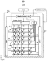
- FIG. 1 is a diagram showing a schematic configuration of a display device in a display device with a sensor according to an embodiment.
- the display device is a liquid crystal display device.
- the display device DSP with a sensor includes a display panel PNL and a backlight BLT that illuminates the display panel PNL from the back side.
- the display panel PNL is provided with a display unit including the display pixels PX arranged in a matrix.
- the gate lines G (G1, G2%) That extend along the rows in which the plurality of display pixels PX are arranged and the sources that extend along the columns in which the plurality of display pixels PX are arranged.
- Lines S (S1, S2%)
- a pixel switch SW arranged near the position where the gate line (scanning line) G and the source line (signal line) S intersect.
- Each of the plurality of display pixels PX has a pixel electrode PE facing the common electrode COME, and has a liquid crystal layer between the pixel electrode PE and the common electrode COME facing each other.
- the common electrode COME includes a plurality of common electrodes Come (Come1, Come2, Come3... ).
- the common electrodes Come extending in the row direction (X direction) are arranged in the column direction (Y direction).
- a plurality of common electrodes Come extending in a plurality of column directions (Y direction) may be arranged in a row direction (X direction).
- a plurality of common electrodes may be arranged in a matrix in a plurality of row directions (X direction) and a plurality of row directions (X direction).
- the pixel switch SW is equipped with a thin film transistor (TFT: Thin Film Transistor).
- TFT Thin Film Transistor
- the gate electrode of the pixel switch SW is electrically connected to the corresponding gate line G.
- the source electrode of the pixel switch SW is electrically connected to the corresponding source line S.
- the drain electrode of the pixel switch SW is electrically connected to the corresponding pixel electrode PE.
- a gate driver GD left side GD-L and right side GD-R
- a source driver SD and a common electrode drive circuit CD are provided as drive means for driving the plurality of display pixels PX.
- Each of the plurality of gate lines G is electrically connected to the output part of the gate driver GD.
- Each of the plurality of source lines S is electrically connected to the output section of the source driver SD.
- the plurality of common electrodes Come are electrically connected to the output section of the common electrode drive circuit CD.
- the source driver SD and the common electrode drive circuit CD are drawn so as to be provided in a drive circuit (Driver circuit).
- a control circuit CTR (Control circuit) that generates a control signal for each of the gate driver GD, the source driver SD, the common electrode drive circuit CD, and the backlight BLT is also provided in the drive circuit (Driver circuit).
- the drive circuit (Driver circuit) is included in a one-chip semiconductor integrated circuit (IC), it may be composed of a plurality of chips. Further, the control circuit CTR (Control circuit) may be provided outside the display panel PNL.
- the gate driver GD, the source driver SD, and the common electrode drive circuit CD are arranged on a peripheral area (frame area) around the display section or on a flexible substrate connected to the display panel PNL.
- the gate driver GD sequentially applies the on-voltage to the plurality of gate lines G, and supplies the on-voltage to the gate electrode of the pixel switch SW electrically connected to the selected gate line G.
- the pixel switch SW whose gate electrode is supplied with the on-voltage is electrically connected between the source electrode and the drain electrode.
- the source driver SD supplies an output signal corresponding to each of the plurality of source lines S.
- the signal supplied to the source line S is supplied to the corresponding pixel electrode PE via the pixel switch SW in which the source electrode and the drain electrode are electrically connected.
- Image signals, control signals, etc. are input to a control circuit CTR (Control circuit) from a host device (Host) provided outside the display panel PNL, and the gate driver GD, the source driver SD, and the common electrode drive circuit CD are displayed on the display panel.
- the operation is controlled by a control circuit CTR (Control circuit) arranged outside or inside the PNL.
- the backlight BLT drives the backlight BLT by a backlight drive circuit (BL drive circuit) based on a backlight control signal generated by a control circuit CTR (Control circuit).
- the backlight drive circuit (BL drive circuit) may be arranged inside the display panel PNL or may be arranged outside the display panel PNL.
- FIG. 2 is a cross-sectional view showing the structure of the sensor-equipped display device according to the embodiment.
- the display device DSP with a sensor has an in-cell type touch sensor, and includes a display panel PNL, a backlight BLT, a first optical element OD1 and a second optical element OD2.
- the display panel PNL is a liquid crystal display panel, but may be another flat panel such as an organic electroluminescence display panel or a micro LED display panel.
- the illustrated display panel PNL has a configuration corresponding to the horizontal electric field mode as a display mode, it may have a configuration corresponding to another display mode.
- the display panel PNL includes a first substrate SUB1, a second substrate SUB2, and a liquid crystal layer LQ.
- the first substrate SUB1 and the second substrate SUB2 are attached to each other with a predetermined cell gap formed.
- the liquid crystal layer LQ is held in the cell gap between the first substrate SUB1 and the second substrate SUB2.
- the first substrate SUB1 is formed by using a light-transmissive first insulating substrate 10 such as a glass substrate or a resin substrate.
- the first substrate SUB1 is on the side of the first insulating substrate 10 facing the second substrate SUB2, the source line S, the common electrode COME, the pixel electrode PE, the first insulating film 11, the second insulating film 12, and the third insulating film. 13, the first alignment film AL1 and the like.
- the pixel electrode PE and the common electrode COME form a display pixel together with the pixel region of the liquid crystal layer arranged between these electrodes, and the display pixels are arranged in a matrix on the display panel PNL.
- the first insulating film 11 is arranged on the first insulating substrate 10. Although not described in detail, the gate line G, the gate electrode of the switching element, the semiconductor layer, and the like are arranged between the first insulating substrate 10 and the first insulating film 11.
- the source line S is formed on the first insulating film 11. Further, the source electrode and the drain electrode of the switching element are also formed on the first insulating film 11. In the illustrated example, the source line S extends in the second direction Y in parallel with the plurality of common electrodes Come.
- the second insulating film 12 is arranged on the source line S and the first insulating film 11.
- the common electrode COME is formed on the second insulating film 12.
- the common electrode COME is divided into a plurality of segments (a plurality of common electrodes Come).
- the respective segments of the common electrode COME extend in the second direction Y and are arranged in the first direction X at intervals.
- Such a common electrode COME is formed of a transparent conductive material such as indium tin oxide (ITO) or indium zinc oxide (IZO).
- ITO indium tin oxide
- IZO indium zinc oxide
- the metal layer ML is formed on the common electrode COME to reduce the resistance of the common electrode COME, but the metal layer ML may be omitted.
- the third insulating film 13 is arranged on the common electrode COME, the metal layer ML, and the second insulating film 12.
- the pixel electrode PE is formed on the third insulating film 13.
- Each pixel electrode PE is located between adjacent source lines S, and faces the common electrode COME. Further, each pixel electrode PE has a slit SL at a position facing the common electrode COME.
- Such a pixel electrode PE is formed of, for example, a transparent conductive material such as ITO or IZO.
- the first alignment film AL1 covers the pixel electrode PE and the third insulating film 13.
- the second substrate SUB2 is formed using the second insulating substrate 20 having a light transmitting property such as a glass substrate or a resin substrate.
- the second substrate SUB2 includes a black matrix BM, color filters CFR, CFG, CFB, an overcoat layer OC, a second alignment film AL2, and the like on the side of the second insulating substrate 20 facing the first substrate SUB1.
- the black matrix BM is formed on the inner surface of the second insulating substrate 20 and partitions each pixel.
- the color filters CFR, CFG, and CFB are each formed on the inner surface of the second insulating substrate 20, and part of them are overlapped with the black matrix BM.
- the color filter CFR is, for example, a red color filter
- the color filter CFG is, for example, a green color filter
- the color filter CFB is, for example, a blue color filter.
- the overcoat layer OC covers the color filters CFR, CFG, and CFB.
- the overcoat layer OC is formed of a transparent resin material.
- the second alignment film AL2 covers the overcoat layer OC.
- the detection electrode DETE is formed on the outer surface of the second insulating substrate 20.
- the detection electrode DETE extends in a direction intersecting each segment of the common electrode COME, and in the illustrated example, extends in the first direction X.
- Such a detection electrode DETE is made of, for example, a transparent conductive material such as ITO or IZO.
- the backlight BLT is arranged on the back side of the display panel PNL.
- various forms can be applied, and any one using a light emitting diode (LED) or a cold cathode tube (CCFL) as a light source can be applied.
- LED light emitting diode
- CCFL cold cathode tube
- the first optical element OD1 is arranged between the first insulating substrate 10 and the backlight BLT.
- the second optical element OD2 is arranged on the detection electrode DETE.
- Each of the first optical element OD1 and the second optical element OD2 includes at least a polarizing plate, and may include a retardation plate as necessary.
- a mutual detection method and a self-detection method are provided as methods for detecting that a user's finger or an external proximity object such as a pen is touching or approaching the touch panel. There are methods.
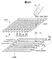
- FIG. 3A is a diagram showing a typical basic configuration of the mutual detection method of the display device with the sensor according to the embodiment.
- the common electrode COME and the detection electrode DETE are used as the sensor.
- the common electrode COME includes a plurality of common electrodes Come (Come1, Come2, Come3... ).
- the plurality of common electrodes Come have, for example, a stripe shape.
- the plurality of common electrodes Come (Come1, Come2, Come3%) are arranged in the scanning (driving) direction (Y direction or X direction).
- the detection electrode DETE includes a plurality of detection electrodes Dete (Dete1, Dete2, Dete3,...) (Thinner than the common electrode).
- the plurality of detection electrodes Dete have, for example, a stripe shape.
- the plurality of detection electrodes Dete (Dete1, Dete2, Dete3,...) Are arranged in a direction (X direction or Y direction) orthogonal to or intersecting with the plurality of common electrodes Come.
- the common electrode COME and the detection electrode DETE are arranged with a space. Therefore, basically, a capacitance Cc (Baseline capacitance) as a capacitance exists between the plurality of common electrodes Come and the plurality of detection electrodes Dete.
- Cc Baseline capacitance
- a predetermined voltage is commonly applied to the plurality of common electrodes Come during the image display period (display period), and a pulsed drive pulse is applied during the touch detection period (detection period). Therefore, in the detection period, each of the plurality of common electrodes Come can be referred to as a drive electrode (Tx). Since the plurality of detection electrodes Dete receive signals from the plurality of common electrodes Come, it can be expressed as Rx (Rx1, Rx2, Rx3,... ).
- a plurality of common electrodes Come, that is, the drive electrodes Tx (Tx1, Tx2, Tx3,%)
- a drive pulse such as an AC voltage in a predetermined cycle.
- a drive pulse Sig
- a pulse-shaped waveform is obtained at the detection electrodes Rx (Rx1, Rx2, Rx3,...)
- another pulse is obtained from the detection electrode Rx2.
- a pulse having an amplitude level lower than that of the pulse obtained from the detection electrode is obtained.
- the detection electrodes Rx (Rx1, Rx2, Rx3,%) Monitor the fringe electric field from the drive electrodes Tx (Tx1, Tx2, Tx3... ), and when a conductor such as a finger approaches, This has the effect of shielding this fringe electric field. Since the fringe electric field is shielded, the detection potential of the detection electrode Rx decreases.
- this difference in detection potential can be treated as a detection pulse of position DETP.
- the illustrated capacitance Cx differs depending on whether the user's finger is close to the detection electrode DETE or far. Therefore, the level of the detection pulse also differs depending on whether the user's finger is close to the detection electrode DETE or far. Therefore, the proximity of the finger to the plane of the touch panel can be determined by the amplitude level of the detection pulse.
- the two-dimensional position of the finger on the plane of the touch panel can be detected by the electrode driving timing by the driving pulse Sig and the output timing of the detection pulse.
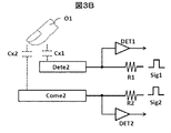
- FIG. 3B is a diagram showing a typical basic configuration of the self (Self) detection method according to the embodiment.
- the self (Self) detection method pulse-shaped self-detection drive pulses are sequentially supplied to the plurality of detection electrodes Dete and the plurality of common electrodes Come to detect the position and coordinates of the user's finger, which is an external proximity object.
- FIG. 3B exemplarily shows the detection electrode Dete2 and the common electrode Come2, and shows a case where the user's finger O1 approaches or contacts the intersection of the detection electrode Dete2 and the common electrode Come2. ing.
- the capacitance of the detection electrode Dete2 by the user's finger O1 becomes a value obtained by adding the self-capacitance of the Dete2 and the capacitance Cx1 by the user's finger O1.
- the electrostatic capacitance of the common electrode Come2 has a value obtained by adding the self-capacitance of the common electrode Come2 and the capacitance Cx2 of the user's finger O1.
- the detection electrode Dete2 is driven by a self-detection drive pulse Sig1 such as an AC voltage via a predetermined impedance R1, and the increased capacitance of the detection electrode Dete2 is driven for self-detection. It is charged by the pulse Sig1.
- the detection circuit DET1 detects that the detection electrode Dete2 has the user's finger O1 based on the value of the charging voltage increased by the capacitance Cx1.
- the common electrode Come2 is driven by a self-detection drive pulse Sig2 such as an AC voltage via a predetermined impedance R2, and the increased capacitance of the common electrode Come2 is charged by the self-detection drive pulse Sig2. ..
- the detection circuit DET2 detects that the detection electrode Dete2 has the user's finger O1 based on the value of the charging voltage increased by the capacitance Cx2. As a result, the presence of the user's finger O1 at the intersection of the detection electrode Dete2 and the common electrode Come2 is detected, and the position and coordinates of the user's finger O1 on the plane of the touch panel are detected.
- the common electrode COME and the detection electrode DETE are used as the sensor as in FIG. 3A.
- the plurality of common electrodes Come that are sequentially driven (scanned) by the self-detection drive pulse Sig2 include a plurality of striped common electrodes (Come1, Come2, Come3,%) As in FIG. 3A.
- the plurality of common electrodes Come are arranged in the Y direction or the X direction.
- the detection electrodes DETE sequentially driven (scanned) by the self-detection drive pulse Sig1 include a plurality of stripe-shaped detection electrodes (Dete1, Dete2, Dete3,...) (Actually, similar to FIG. 3A. (Thinner than the striped common electrode).
- the plurality of detection electrodes Dete are arranged in a direction (X direction or Y direction) orthogonal to or intersecting with the plurality of common electrodes Come.
- the plurality of detection electrodes Dete and the plurality of common electrodes Come.
- the position of the external proximity object O1 at the intersection of can be detected.
- the plurality of detection electrodes Dete and the plurality of common electrodes Come can all be regarded as detection electrodes.
- the touch sensor when the touch sensor is in the low power consumption mode, only the detection electrode DETE is driven by the self-detection drive pulse Sig1 to detect only the presence or absence of an external proximity object such as a finger and switch to mutual detection.
- the coordinates of the external proximity object may be detected.
- the plurality of common electrodes Come are individually arranged in a matrix in the row direction (X direction) and the column direction (Y direction), and the self-detection method using only the plurality of common electrodes Come is adopted.
- the coordinates of an external proximity object such as a finger may be detected.
- a configuration may be used in which a mutual detection method and a self detection method can be switched by a switch or the like.
- the configuration of the self-detection method shown in FIG. 3B is an example, and the configuration is not limited to this.
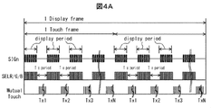
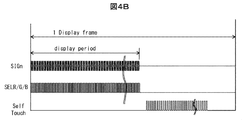
- FIG. 4A and FIG. 4B are diagrams for explaining driving methods of the mutual detection method and the self-detection method of the sensor-equipped display device according to the embodiment.
- the common electrode COME used for image display is also used as the electrode for touch position detection, the image display operation and the touch position detection operation are driven in time division (time sharing).
- a period for displaying an image and a period for detecting a touch position are each divided, and the divided image display period and the divided touch position detection period are alternately repeated to display one frame.
- Configure the period That is, after the operation of outputting the video signal (SIGNn) for each color corresponding to the signal (SELR/G/B) for selecting three colors of RGB is executed for the plurality of divided display rows, the divided plural
- the mutual detection operation of inputting the drive pulse Sig to the drive electrode Tx of is executed. Then, this operation is sequentially and repeatedly performed for the plurality of divided display rows and the plurality of drive electrodes Tx.
- touch detection for two frames is performed during one frame display period.
- the drive electrodes Tx1, Tx2, Tx3,... Are sequentially scanned by the drive pulse Sig to detect the touch position.
- the self-detection drive pulse (Sig1) is input to all the detection electrodes DETE to execute the self-detection operation. That is, after performing the operation of outputting the video signal (SIGNn) for each color corresponding to the signal (SELR/G/B) for selecting the three colors of RGB for all the display rows, the self detection is performed for all the detection electrodes DETE.
- the detection drive pulse (Sig1) is input to execute the self-detection operation.
- the self-detection method is a method capable of sensing with higher sensitivity than the mutual detection method. The method is not limited to the method of FIG. 4B, and self-sensing may be performed during the detection period shown in FIG. 4A (division method).
- the common electrodes Come1, Come2, Come3,... are denoted by the symbols of the drive electrodes Tx1, Tx2, Tx3,.
- the plurality of detection electrodes Dete1, Dete2, Dete3,... are denoted by symbols Rx1, Rx2, Rx3,.
- the drive electrodes (Tx1, Tx2, etc.) are drawn by dotted lines
- the detection electrodes (Rx1, Rx2, etc.) are drawn by solid lines for easy understanding and easy viewing of the drawing.
- the lead lines (W11, W12, etc.) are drawn by thin solid lines.
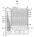
- FIG. 5 is a plan view conceptually showing a configuration example of the sensor in the display device with the sensor according to the embodiment.
- the sensor-equipped display device DSP has a display panel PNL including an active area (touch detection area) AA of the sensor and a peripheral area (frame area) provided around the active area AA.
- the display panel PNL has a first side (left side), a second side (right side) opposite to the first side, and a third side (upper side) provided between the first side and the second side. And a fourth side (lower side) opposite to the third side.
- the peripheral area (frame area) around the active area (touch detection area) AA of the sensor is exemplified by a left frame area E1 and a right frame area E2.
- a plurality of detection electrodes Rx1, Rx2, Rx3,..., Rx8 arranged in parallel in the direction are provided.
- a plurality of lead wirings W11, W12, W13, W14,..., respectively coupled to the plurality of detection electrodes Rx1, Rx2, Rx3,. W18 is provided.
- the plurality of lead wires W11, W12, W13, W14,..., W18 are electrically connected to a touch detection circuit (touch controller, control circuit) TC.
- the plurality of drive electrodes Tx1, Tx2, Tx3,..., Tx8 are electrically connected to the display control device DI via a plurality of lead wirings W2 and a common electrode drive circuit CD (not shown), and a touch sensor.
- the common electrode drive circuit CD is sequentially driven by the drive pulse Sig in accordance with an instruction from the display control device DI.
- the touch detection circuit TC may be provided in the display control device DI.
- FIG. 6 is a plan view conceptually showing another configuration example of the sensor in the sensor-attached display device according to the embodiment.
- FIG. 6 is a display device DSP with a sensor that can be used in a self (Self) detection method, and includes a plurality of electrodes Sx11, Sx12, Sx13, Sx21, Sx22, Sx23,. . . , Sx81, Sx82, Sx83 are formed as individual electrodes arranged in a matrix on the active area (touch detection area) AA of the sensor.
- the plurality of electrodes Sx11 to Sx83 for the sensor function as the common electrode COME for display during the image display period, and have the functions of the drive electrode and the detection electrode during the detection period of the touch sensor.
- the electrodes Sx11 to Sx83 for sensors will be described as drive electrodes.
- a plurality of pixels PX are formed to face the drive electrodes Sx11 to Sx83.
- the drive electrodes Sx11 to Sx83 include a plurality of lead wires W11, W12, W13, W21, W22, W23,. . . , W81, W82, W83 are electrically connected to the display control device DI.
- the drive electrodes Sx11 to Sx83 are sequentially driven by drive pulses from the common electrode drive circuit CD according to an instruction from the display control device DI during the detection period of the touch sensor.
- the detection signals from the individual electrodes of the drive electrodes Sx11 to Sx83 are extracted wirings W11, W12, W13, W21, W22, W23,.
- the drive electrodes Sx11 to Sx83 function as the common electrode COME during the video display period, and a predetermined voltage (VCOM) is applied.
- FIG. 7 is a diagram showing an input/output circuit according to a comparative example.
- FIG. 8 is a diagram illustrating drive electrodes having different areas according to the embodiment.
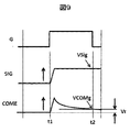
- FIG. 9 is a diagram showing a timing chart in the video display period.
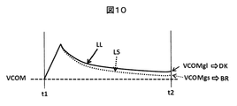
- FIG. 10 is a waveform diagram showing the potential change of the shared electrode of FIG. 9 based on the area of the drive electrode.
- FIG. 11 is a diagram showing a display example of a display panel having drive electrodes having different areas.
- FIG. 12 is a diagram for explaining a difference in waveform of drive pulses of drive electrodes having different areas in the detection period.
- an input/output circuit IOC connected to one drive electrode in FIG. 6 is shown as a typical example.
- the input/output circuit IOC electrically connected to the drive electrode Sx11 is shown.
- the input/output circuit IOC is electrically connected to the drive electrode Sx11 via the resistance element Ro, the external terminal Tex, and the lead wire W11.
- the external terminal Tex is an external connection pad provided in the display control device DI.
- the input/output circuit IOC includes a drive circuit AMP1, a drive circuit AMP2, a detection circuit DET, and switches SW1 to SW3.
- the switch SW1 is selectively closed (ON), and the drive circuit AMP1 outputs a predetermined voltage (VCOM) to the drive electrode Sx11 via the closed switch SW1.
- VCOM predetermined voltage
- the switches SW2 and SW3 are open (off).
- the switches SW2 and SW3 are selectively closed (ON) and the switch SW1 is open (OFF).
- the drive circuit AMP2 outputs a drive pulse to the drive electrode Sx11 via the closed switch SW2.
- the detection circuit DET detects the capacitance change of the drive electrode Sx11 as a detection voltage via the closed switch SW3.
- FIG. 8 is a plan view showing drive electrodes of a mobile terminal equipped with a camera and the like.
- the display panel PNL of the mobile terminal has a rectangular shape in a plan view.
- the display panel PNL of the mobile terminal may be provided with a notch portion NTC or a hole portion HOL in order to mount a camera.
- the area (S1) of the two drive electrodes SxN provided in the notch portion NTC and the hole portion HOL are provided.
- the area (S2, S2>S1) of the four drive electrodes SxH is smaller than the area (S3) of the normal drive electrode Sxn where the notch portion NTC and the hole portion HOL are not provided (S1 ⁇ S2 ⁇ S3).
- the shape of the drive electrode SxC provided at the four corners also corresponds to the shape of the display section of the display panel.
- the area (S4) of the drive electrode SxC is smaller than the area (S3) of the normal drive electrode Sxn (S4 ⁇ S3). That is, a plurality of drive electrodes (SxN, SxH, SxC, Sxn) having different areas are provided in one display panel.
- the relationship of the areas of the drive electrodes is described as S1 ⁇ S2 ⁇ S4 ⁇ S3, but the present invention is not limited to this.
- the gate electrode G transits from the low level to the high level at time t1
- the pixel switch SW is turned on, and the video signal SIG supplied to the source line S is supplied to the display pixel PX.
- the potential VCOM of the common electrode COME temporarily rises based on the rise of the potential of the video signal SIG due to the coupling capacitance between at least one of the source line S and the pixel electrode PE and the common electrode COME, and then, Gradually descend.
- the pixel switch SW is turned off, and the potential difference between the potential VSig of the video signal SIG and the potential VCOMg of the common electrode COME at this time is applied to the display pixel PX. It will be stored as a video signal.
- the potential VCOMg of the common electrode COME does not completely return to the original potential but has some potential, and this potential is the unconverged potential Vr. I have to say.
- FIG. 10 shows the waveforms of the drive electrodes Sx (Sx11, Sx12, Sx13,... ).
- the drive electrodes Sx (Sx11, Sx12, Sx13,...) For touch detection are a plurality of common electrodes Come for display.
- the area of the drive electrode Sx is large, the potential VCOM of the drive electrode Sx changes as shown by the solid line LL.
- the area of the drive electrode Sx is small, it changes as shown by the dotted line LS. It is considered that this is because the time constant differs between the case where the area of the drive electrode Sx is large and the case where it is small, due to the difference in the capacitance value parasitic on the drive electrode Sx.
- the two drive electrodes SxN provided in the notch portion NTC, the four drive electrodes SxH provided around the hole portion HOL, and the drive electrodes SxC provided at the four corners of the display panel have small areas. Minute, the time constant becomes smaller. Since the time constant is small, the potential VCOMgs of the drive electrode Sx becomes lower than the potential VCOMgl of the drive electrode Sxn having a large area. As a result, the display pixel PX corresponding to the drive electrode Sxn having a large area becomes dark (DK), and the display pixel PX corresponding to the drive electrode (SxN, SxN, SxC) having a small area corresponds to the drive electrode Sxn having a large area.
- the display pixel PX becomes brighter (BR) than the display pixel PX.
- the display pixels PX corresponding to the drive electrodes (SxN, SxN, SxC) having a small area may become bright (BR) and may look like a block. ..
- the waveform of the drive pulse during the detection period will differ due to the difference between the time constants of the drive electrodes (SxN, SxN, SxC) having a small area and the time constants of the drive electrodes (Sxn) having a large area. That is, as shown in FIG. 12, the waveform of the charge amount Q by the drive pulse for the drive electrodes (SxN, SxN, SxC) having a small area changes rapidly as shown by the dotted line LS2. On the other hand, the waveform of the charge amount Q due to the drive pulse for the drive electrode (Sxn) having a large area changes late as shown by the solid line LL2 as compared with the dotted line LS2. As a result, an erroneous determination of touch detection may occur during the detection period.
- FIG. 13 is a diagram showing an input/output circuit including a time constant adjusting circuit according to the embodiment. 13 is different from FIG. 7 in that a time constant adjusting circuit TCC is provided between the input/output circuit IOC and the external terminal Tex.
- the time constant adjustment circuit TCC includes a plurality of switch elements SWa, SWb, SWc, SWd and a plurality of resistance elements Rb, Rc, Rd.
- the switch element SWa is provided between the input/output circuit IOC and the external terminal Tex without the resistance element.
- the switch element SWb and the resistance element Rb are connected in series between the input/output circuit IOC and the external terminal Tex.
- the switch element SWc and the resistance element Rc are connected in series between the input/output circuit IOC and the external terminal Tex.
- the switch element SWd and the resistance element Rd are connected in series between the input/output circuit IOC and the external terminal Tex.
- FIG. 13 further shows a register REG provided in the display control device DI.
- the register REG can set control data by an instruction in order to control the ON state and the OFF state of each of the plurality of switch elements SWa, SWb, SWc, and SWd.
- the control data set in the register REG controls the ON state and the OFF state of each of the plurality of switch elements SWa, SWb, SWc, and SWd.
- the resistance value between the input/output circuit IOC and the external terminal Tex can be adjusted by the time constant adjustment circuit TCC by controlling the ON state and the OFF state of the plurality of switch elements SWa, SWb, SWc, and SWd. It is possible to adjust the time constant between the input/output circuit IOC and the drive electrode Sx11.
- the time constant between the input/output circuit IOC and the drive electrode (Sxn) having a large area is matched with the time constant between the input/output circuit IOC and the drive electrode (SxN, SxN, SxC) having a small area.
- the time constant is adjusted by the time constant adjusting circuit TCC.
- FIG. 13 exemplarily shows the state of the time constant adjustment circuit TCC in the case where the drive electrode Sx11 is the drive electrode SxC in the corner portion.
- the switch element SWa is in the off state
- the switch elements SWb, SWc, SWd are in the on state.
- the time constants corresponding to the resistance elements Rb, Rc, and Rd are added to the drive electrode SxC.
- the time constant adjustment circuit TCC adds a time constant of R/3 between the input/output circuit IOC and the drive electrode Sx11.
- drive electrodes Sx11 to Sx83, SxN, SxN, SxC, and Sxn shown in FIGS. 6 and 8 are described with reference to FIG. 13, the present invention is not limited to this. It is also applicable to the drive circuit for the drive electrodes Tx1 to TX8 and the detection electrodes Rx1 to Rx8 shown in FIG.
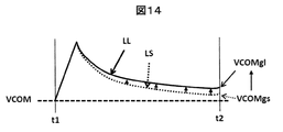
- FIG. 14 is a waveform diagram illustrating a potential change of the common electrode Come in the video display period when the time constant adjustment circuit is used.
- FIG. 15 is a waveform diagram of the drive pulse of the drive electrode in the detection period when the time constant adjusting circuit is used.
- the drive electrodes Sx (Sx11, Sx12, Sx13,%) For touch detection are a plurality of common electrodes Come for display.
- the brightness of the display pixel PX corresponding to the drive electrode Sxn having a large area and the brightness of the display pixel PX corresponding to the drive electrode (SxN, SxN, SxC) having a small area can be substantially equalized. That is, it is possible to prevent the block-like appearance.
- the drive electrodes having a small area As shown in FIG. 15, when the time constant between the input/output circuit IOC and the drive electrodes (SxN, SxN, SxC) having a small area is adjusted by the time constant adjusting circuit TCC, the drive electrodes having a small area ( The difference in potential level between the waveforms LS2 and LL2 is improved so that the waveform LS2 in the case of SxN, SxN, SxC) matches the waveform LL2 in the case of the drive electrode Sxn having a large area. This can reduce the possibility of erroneous touch detection during the detection period.
- FIG. 16 is a diagram showing a state of the time constant adjustment circuit and its equivalent circuit when the drive electrode shown in FIG. 8 is driven.
- the left side shows the ON state and the OFF state of the switch elements SWa, SWb, SWc, and SWd of the time constant adjustment circuit TCC for each drive electrode.
- an equivalent circuit of the time constant added by the time constant adjusting circuit TCC for each drive electrode is shown on the right side.
- the values of the resistance elements Rb, Rc, and Rd are considered to be the same value R will be described.
- the time constant adjustment circuit TCC corresponding to the drive electrodes SxC provided at the four corners of the display panel PNL, the switch elements SWa, SWb, SWc, SWd are turned off, on, on, and on. Therefore, in this case, the time constant adjusting circuit TCC adds a time constant of R/3.
- the time constant adjustment circuit TCC corresponding to the four drive electrodes SxH provided around the hole portion HOL, the switch elements SWa, SWb, SWc, and SWd are turned off, off, on, and on. Therefore, in this case, the time constant adjusting circuit TCC adds a time constant of R/2.
- the switch elements SWa, SWb, SWc, SWd are turned on, off, off, and off. Therefore, in this case, the time constant is not added by the time constant adjusting circuit TCC (0).
- the time constant adjustment circuit TCC corresponding to the two drive electrodes SxN provided in the notch portion NTC, the switch elements SWa, SWb, SWc, SWd are turned off, on, off, and off. Therefore, in this case, the time constant adjusting circuit TCC adds the time constant of R.
- time constant adjustment circuits TCC are provided.
- the time constant of (0, R, R/2, R/3) is adjustable.
- the time constant adjustment circuit TCC may be configured to be able to adjust N types of time constants.
- the resistance elements Rb, Rc, and Rd may have different values so that the time constants can be set to be substantially the same according to the areas or area ratios of the different N drive electrodes.
- the time constant adjustment circuit TCC is provided in the drive circuit (IOC) corresponding to all the drive electrodes provided in the display panel PNL. Therefore, it is possible to flexibly deal with the number and arrangement position of the notch portions NTC and the number and arrangement position of the hole portions HOL provided in the display panel PNL.
- FIG. 17 is a diagram showing a time constant adjusting circuit according to the first modification.
- the time constant adjusting circuit TCC shown in FIG. 13 adjusts the time constant by the resistance elements Rb, Rc, and Rd.
- the time constant is adjusted by the plurality of capacitive elements Cb, Cc, Cd.
- the capacitance elements Cb, Cc, Cd control the on-state and off-state of the switch elements SWb, SWc, SWd, respectively, so that the capacitance value between the input/output circuit IOC and the external terminal Tex becomes constant.
- Can be adjusted by This makes it possible to adjust the time constant between the input/output circuit IOC and the drive electrode Sx11.
- FIG. 18 is a diagram showing a time constant adjusting circuit according to the second modification.
- the time constant adjustment circuit TCC shown in FIG. 18 is shown in FIG. 17 in addition to the plurality of switch elements SWa, SWb, SWc, SWd and the plurality of resistance elements Rb, Rc, Rd shown in FIG.
- Such switch elements SWe and SWf and capacitive elements Ce and Cf are provided. That is, by controlling the ON state and the OFF state of each of the switch elements SWa, SWb, SWc, SWd, SWe, and SWf, the time constant by the resistance element (Rb, Rc, Rd) and the capacitance element (Ce, Cf) It is possible to adjust the time constant and.
- Modification 3 In the configuration shown in FIG. 16, a configuration example in which the time constant adjustment circuit TCC is provided for all the drive electrodes provided in the display panel PNL has been shown. However, if the time constant adjustment circuits TCC are provided for all the drive electrodes, it is considered that the chip area of the display control device DI increases. In Modification 3, a configuration example in which the time constant adjustment circuit TCC is provided only for a specific drive electrode will be described.
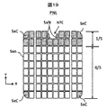
- FIG. 19 is a plan view of the drive electrode when one notch portion NTC is provided on the upper side of the display panel PNL.
- FIG. 20 is a plan view of the drive electrode when one hole portion HOL is provided on the upper side of the display panel PNL.
- the notch portion NTC and the hole portion HOL are often provided on the upper side of the display panel PNL.
- the notch portion NTC and the hole portion HOL are highly likely to be provided mainly in the upper 1 ⁇ 5 region when the display panel PNL is divided in the Y direction, for example, into five equal parts, and the lower part There is a high possibility that it will not be provided in the 4/5 area.
- the drive electrodes SxC located at the four corners of the display panel PNL are likely to be drive electrodes having a smaller area than the area of the drive electrodes Sxn according to the outer shape of the display panel PNL.
- FIG. 19 and FIG. 20 with respect to the drive electrodes indicated by hatching (the drive electrodes provided in the upper 1 ⁇ 5 region of the display panel PNL and the drive electrodes SxC at the lower two corners).
- the time constant control circuit TCC may be added, and the time constant control circuit TCC may not be added to the other white drive electrodes without shading.
- FIG. 21 is a diagram showing a circuit configuration for the drive electrodes indicated by hatching and the other drive electrodes.
- hatched drive electrodes drive electrodes (SxC, Sxn, SxN, or SxH) provided in the upper 1 ⁇ 5 region of the display panel PNL) and two lower corners
- a time constant control circuit TCC is provided for the drive electrode (SxC).
- the time constant control circuit TCC is not added to the other white drive electrodes (Sxn) which are not shaded.
- the time constant control circuit TCC shown in FIG. 13, FIG. 17 or FIG. 18 can be used.
- the number of time constant adjustment circuits TCC provided in the display control device DI can be reduced to about 1/5, and an increase in the chip area of the display control device DI can be reduced.
- the number of bits of the register REG for controlling the time constant adjusting circuit TCC provided in the display control device DI can be reduced to about 1/5 as compared with FIG. Therefore, the operation of setting the control data in the register REG by the instruction can also be performed in a short time.
- the notch portion NTC and the hole portion HOL can be arbitrarily arranged and the arrangement position and the number can be determined in the upper 1 ⁇ 5 region of the display panel PNL, the degree of freedom in designing the display panel PNL is not hindered.
- the area is 1 ⁇ 5 above the display panel PNL, but the invention is not limited to this.
- a time constant can be added by a time constant adjusting circuit TCC to at least four corner drive electrodes (SxC) and drive electrodes in regions where notches NTC and hole HOL are expected to be formed. do it.
- Various inventions can be formed by appropriately combining a plurality of constituent elements disclosed in the above embodiments. For example, some components may be deleted from all the components shown in the embodiment. Furthermore, the constituent elements of different embodiments may be combined appropriately.
- DSP Display device PNL: Display panel DI: Display control device IOC: Input/output circuit AMP1, AMP2: Drive circuit DET: Detection circuit NTC: Notch part HOL: Hole part Sx, SxN, SxH, SxC, Sxn: Drive electrode TCC: Time constant adjusting circuit Rb, Rc, Rd: Resistance element SWa, SWb, SWc, SWd: Switching element Cb, Cc, Cd, Ce, Cf: Capacitance element REG: Register
Landscapes
- Engineering & Computer Science (AREA)
- Physics & Mathematics (AREA)
- General Physics & Mathematics (AREA)
- Theoretical Computer Science (AREA)
- Nonlinear Science (AREA)
- Crystallography & Structural Chemistry (AREA)
- Chemical & Material Sciences (AREA)
- General Engineering & Computer Science (AREA)
- Computer Hardware Design (AREA)
- Optics & Photonics (AREA)
- Mathematical Physics (AREA)
- Human Computer Interaction (AREA)
- Liquid Crystal (AREA)
- Liquid Crystal Display Device Control (AREA)
- Control Of Indicators Other Than Cathode Ray Tubes (AREA)
- Devices For Indicating Variable Information By Combining Individual Elements (AREA)
Abstract
本開示の目的は、表示むらを改善可能な表示装置を提供することにある。表示装置は、複数の駆動回路と、前記複数の駆動回路の出力に各々接続される複数の駆動電極と、を含む。前記複数の駆動電極内の少なくとも1つの駆動電極の面積は、他より小さい。面積が小さい前記少なくとも1つの駆動電極に対応する駆動回路の出力の時定数を調整するための時定数調整回路を有する。
Description
本発明は表示装置に関し、特に、タッチセンサを備えた表示装置に適用可能である。
液晶表示パネルの内部にタッチパネルを内蔵したインセル方式の液晶表示装置が提案されている(たとえば、特開2014-102665号公報)。インセル方式の場合、複数の共通電極は、映像表示期間には共通して所定の電圧が印加され、タッチ検出期間にはパルス状の駆動パルスが印加される。そのため、検出期間においては、共通電極はタッチ検出用の駆動電極として利用される。
表示装置等の携帯機器において複数の駆動電極内の1部の駆動電極は、その面積を小さくする場合がある。面積が小さい駆動電極の時定数は、他の駆動電極の時定数と比較して、小さくなる。映像表示期間において、複数の駆動電極(共通電極)には、共通して所定の電圧(VCOM)が印加される。複数の共通電極間においてその時定数が異なると、表示パネルの表示品質が低下するという課題がある。
本発明の目的は、表示むらを改善可能な表示装置を提供することにある。
その他の課題と新規な特徴は、本明細書の記述および添付図面から明らかになるであろう。
本発明のうち代表的なものの概要を簡単に説明すれば下記の通りである。
すなわち、表示装置は、複数の駆動回路と、前記複数の駆動回路の出力に各々接続される複数の駆動電極と、を含む。前記複数の駆動電極内の少なくとも1つの駆動電極の面積は、他より小さい。面積が小さい前記少なくとも1つの駆動電極に対応する駆動回路の出力の時定数を調整するための時定数調整回路を有する。
以下に、本発明の実施の形態および変形例について、図面を参照しつつ説明する。
なお、開示はあくまで一例にすぎず、当業者において、発明の主旨を保っての適宜変更について容易に想到し得るものについては、当然に本発明の範囲に含有されるものである。また、図面は説明をより明確にするため、実際の態様に比べ、各部の幅、厚さ、形状等について模式的に表される場合があるが、あくまで一例であって、本発明の解釈を限定するものではない。
また、本明細書と各図において、既出の図に関して前述したものと同様の要素には、同一の符号を付して、詳細な説明を適宜省略することがある。
本実施形態においては、表示装置の一例として、液晶表示装置を開示する。この液晶表示装置は、例えば、スマートフォン、タブレット端末、携帯電話端末、パーソナルコンピュータ、テレビ受像装置、車載装置、ゲーム機器等の種々の装置に用いることができる。
「表示装置」とは、表示パネルを用いて映像を表示する表示装置全般を指す。「表示パネル」とは、電気光学層を用いて映像を表示する構造体を指す。例えば、表示パネルという用語は、電気光学層を含む表示セルを指す場合もあるし、表示セルに対して他の光学部材(例えば、偏光部材、バックライト、タッチパネル等)を装着した構造体を指す場合もある。ここで、「電気光学層」には、技術的な矛盾を生じない限り、液晶層、エレクトロクロミック(EC)層などが含まれ得る。したがって、後述する実施形態について、表示パネルとして、液晶層を含む液晶パネルを例示して説明するが、上述した他の電気光学層を含む表示パネルへの適用を排除するものではない。
(実施形態)
図1は、実施の形態のセンサ付き表示装置における表示装置の概略の構成を示す図である。なお、実施の形態において、表示装置は液晶表示装置である。
図1は、実施の形態のセンサ付き表示装置における表示装置の概略の構成を示す図である。なお、実施の形態において、表示装置は液晶表示装置である。
センサ付き表示装置DSPは、表示パネルPNLと、表示パネルPNLを背面側から照明するバックライトBLTと、を備えている。そして表示パネルPNLには、マトリクス状に配置された表示画素PXを含む表示部が設けられている。
図1に示すように、表示部においては、複数の表示画素PXが配列する行に沿って延びるゲート線G(G1、G2…)と、複数の表示画素PXが配列する列に沿って延びるソース線S(S1、S2…)と、ゲート線(走査線)Gとソース線(信号線)Sが交差する位置近傍に配置された画素スイッチSWとが備えられている。複数の表示画素PXの各々は共通電極COMEに対向した画素電極PEを有し、対向する画素電極PEと共通電極COMEの間に液晶層を有する。共通電極COMEは複数の共通電極Come(Come1,Come2,Come3・・・・)を含む。複数の行方向(X方向)に延在された複数の共通電極Comeは列方向(Y方向)に配置される。尚、複数の列方向(Y方向)に延在された複数の共通電極Comeを行方向(X方向)に配置する構成としてもよい。また、複数の共通電極を複数の行方向(X方向)と複数の行方向(X方向)にマトリックス状に配置してもよい。
画素スイッチSWは薄膜トランジスタ(TFT:Thin Film Transistor)を備えている。画素スイッチSWのゲート電極は対応するゲート線Gと電気的に接続されている。画素スイッチSWのソース電極は対応するソース線Sと電気的に接続されている。画素スイッチSWのドレイン電極は対応する画素電極PEと電気的に接続されている。
また、複数の表示画素PXを駆動する駆動手段として、ゲートドライバGD(左側GD-Lおよび右側GD-R)、ソースドライバSD、共通電極駆動回路CDとが設けられている。複数のゲート線Gは各々ゲートドライバGDの出力部と電気的に接続されている。複数のソース線Sは各々ソースドライバSDの出力部と電気的に接続されている。複数の共通電極Comeは共通電極駆動回路CDの出力部と電気的に接続されている。図1においては、ソースドライバSDと共通電極駆動回路CDとが、駆動回路(Driver circuit)内に設けられるように描かれている。各々のゲートドライバGD、ソースドライバSD、共通電極駆動回路CD、およびバックライトBLTの制御信号を生成する制御回路CTR(Control circuit)も駆動回路(Driver circuit)内に設けられる。尚、駆動回路(Driver circuit)は1チップの半導体集積回路(IC)に含まれるが、複数のチップで構成されるようにしてもよい。また、制御回路CTR(Control circuit)は表示パネルPNLの外部に設けるようにしてもよい。
ゲートドライバGDとソースドライバSDと共通電極駆動回路CDとは、表示部の周囲の周辺領域(額縁領域)あるいは表示パネルPNLに接続されたフレキシブル基板上に配置される。ゲートドライバGDは複数のゲート線Gにオン電圧を順次印加して、選択されたゲート線Gに電気的に接続された画素スイッチSWのゲート電極にオン電圧を供給する。ゲート電極にオン電圧が供給された画素スイッチSWの、ソース電極-ドレイン電極間が導通する。ソースドライバSDは、複数のソース線Sのそれぞれに対応する出力信号を供給する。ソース線Sに供給された信号は、ソース電極-ドレイン電極間が導通した画素スイッチSWを介して対応する画素電極PEに供給される。
表示パネルPNLの外部に設けられたホスト装置(Host)から画像信号、制御信号等が制御回路CTR(Control circuit)に入力され、ゲートドライバGDとソースドライバSDと共通電極駆動回路CDは、表示パネルPNLの外部あるいは内部に配置された制御回路CTR(Control circuit)により動作を制御される。バックライトBLTは制御回路CTR(Control circuit)で生成されたバックライト制御信号に基づいてバックライト用駆動回路(BL drive circuit)にてバックライトBLTの駆動を行う。バックライト用駆動回路(BL drive circuit)は表示パネルPNLの内部に配置されてもよいし、表示パネルPNLの外部に配置されてもよい。
図2は、実施の形態のセンサ付き表示装置の構造を示す断面図である。
センサ付き表示装置DSPは、インセル型のタッチセンサを有するものであり、表示パネルPNL、バックライトBLT、第1光学素子OD1及び第2光学素子OD2を備えている。図示した例では、表示パネルPNLは、液晶表示パネルであるが、有機エレクトロルミネッセンス表示パネル、マイクロLED表示パネルなどの他のフラットパネルであっても良い。また、図示した表示パネルPNLは、表示モードとして横電界モードに対応した構成を有しているが、他の表示モードに対応した構成を有していても良い。
表示パネルPNLは、第1基板SUB1、第2基板SUB2、及び、液晶層LQを備えている。第1基板SUB1と第2基板SUB2とは所定のセルギャップを形成した状態で貼り合わされている。液晶層LQは、第1基板SUB1と第2基板SUB2との間のセルギャップに保持されている。
第1基板SUB1は、ガラス基板や樹脂基板などの光透過性を有する第1絶縁基板10を用いて形成されている。第1基板SUB1は、第1絶縁基板10の第2基板SUB2に対向する側に、ソース線S、共通電極COME、画素電極PE、第1絶縁膜11、第2絶縁膜12、第3絶縁膜13、第1配向膜AL1などを備えている。
ここで、画素電極PE及び共通電極COMEは、これら電極間に配置される液晶層の画素領域とともに表示画素を構成し、表示画素は表示パネルPNLにマトリクス状に配置されている。
第1絶縁膜11は、第1絶縁基板10の上に配置されている。なお、詳述しないが、第1絶縁基板10と第1絶縁膜11との間には、ゲート線G、スイッチング素子のゲート電極や半導体層などが配置されている。ソース線Sは、第1絶縁膜11の上に形成されている。また、スイッチング素子のソース電極やドレイン電極なども第1絶縁膜11の上に形成されている。図示した例では、ソース線Sは、複数の共通電極Comeと平行して第2方向Yに延出している。
第2絶縁膜12は、ソース線S及び第1絶縁膜11の上に配置されている。共通電極COMEは、第2絶縁膜12の上に形成されている。図示した例では、共通電極COMEは、複数のセグメント(複数の共通電極Come)に分割されている。共通電極COMEの各セグメントは、それぞれ第2方向Yに延出し、間隔をおいて第1方向Xに並んでいる。このような共通電極COMEは、インジウム・ティン・オキサイド(ITO)やインジウム・ジンク・オキサイド(IZO)などの透明な導電材料によって形成されている。なお、図示した例では、共通電極COMEの上に金属層MLが形成され、共通電極COMEを低抵抗化しているが、金属層MLは省略しても良い。
第3絶縁膜13は、共通電極COME、金属層ML、及び第2絶縁膜12の上に配置されている。画素電極PEは、第3絶縁膜13の上に形成されている。各画素電極PEは、隣接するソース線Sの間にそれぞれ位置し、共通電極COMEと対向している。また、各画素電極PEは、共通電極COMEと対向する位置にスリットSLを有している。このような画素電極PEは、例えば、ITOやIZOなどの透明な導電材料によって形成されている。第1配向膜AL1は、画素電極PE及び第3絶縁膜13を覆っている。
一方、第2基板SUB2は、ガラス基板や樹脂基板などの光透過性を有する第2絶縁基板20を用いて形成されている。第2基板SUB2は、第2絶縁基板20の第1基板SUB1に対向する側に、ブラックマトリクスBM、カラーフィルタCFR、CFG、CFB、オーバーコート層OC、第2配向膜AL2などを備えている。
ブラックマトリクスBMは、第2絶縁基板20の内面に形成され、各画素を区画している。カラーフィルタCFR、CFG、CFBは、それぞれ第2絶縁基板20の内面に形成され、それらの一部がブラックマトリクスBMに重なっている。カラーフィルタCFRは例えば赤色カラーフィルタであり、カラーフィルタCFGは例えば緑色カラーフィルタであり、カラーフィルタCFBは例えば青色カラーフィルタである。オーバーコート層OCは、カラーフィルタCFR、CFG、CFBを覆っている。オーバーコート層OCは、透明な樹脂材料によって形成されている。第2配向膜AL2は、オーバーコート層OCを覆っている。
検出電極DETEは、第2絶縁基板20の外面に形成されている。この検出電極DETEは、共通電極COMEの各セグメントと交差する方向に延出しており、図示した例では、第1方向Xに延出している。このような検出電極DETEは、例えば、ITOやIZOなどの透明な導電材料によって形成されている。
バックライトBLTは、表示パネルPNLの背面側に配置されている。バックライトBLTとしては、種々の形態が適用可能であり、光源として発光ダイオード(LED)を利用したものや冷陰極管(CCFL)を利用したものなどのいずれでも適用可能である。
第1光学素子OD1は、第1絶縁基板10とバックライトBLTとの間に配置されている。第2光学素子OD2は、検出電極DETEの上に配置されている。第1光学素子OD1及び第2光学素子OD2は、それぞれ少なくとも偏光板を含んでおり、必要に応じて位相差板を含んでいても良い。
次に、センサ付き表示装置DSPに用いられるタッチセンサについて説明する。タッチセンサにおいて、タッチパネルに対して利用者の指或いはペン等の外部近接物体が触れていること、或いは近接していることを検出する方式として、ミューチャル(Mutual)検出方式と、セルフ(Self)検出方式と、がある。
<ミューチャル(Mutual)検出方式>
図3Aは、実施の形態に係るセンサ付き表示装置のミューチャル検出方式の代表的な基本構成を示す図である。センサとしては、共通電極COMEと検出電極DETEとが利用される。
図3Aは、実施の形態に係るセンサ付き表示装置のミューチャル検出方式の代表的な基本構成を示す図である。センサとしては、共通電極COMEと検出電極DETEとが利用される。
共通電極COMEは、複数の共通電極Come(Come1,Come2,Come3・・・・)を含む。複数の共通電極Comeは、例えば、ストライプ状とされる。この複数の共通電極Come(Come1,Come2,Come3・・・・)が走査(駆動)方向(Y方向またはX方向)に配列されている。
一方、検出電極DETEは、複数の検出電極Dete(Dete1,Dete2,Dete3,・・・・)(共通電極よりも細い)を含む。複数の検出電極Deteは、例えば、ストライプ状とされる。この複数の検出電極Dete(Dete1,Dete2,Dete3,・・・・)は、複数の共通電極Comeと直交あるいは交差する方向(X方向またはY方向)に配列されている。
共通電極COMEと検出電極DETEは、間隔を置いて配置される。このために、複数の共通電極Comeと、複数の検出電極Deteとの間には、基本的に静電容量としての容量Cc(Baseline容量)が存在する。
複数の共通電極Comeは映像表示期間(表示期間)には共通して所定の電圧が印加され、タッチ検出期間(検出期間)にはパルス状の駆動パルスが印加される。そのため、検出期間においては、複数の共通電極Comeの各々は駆動電極(Tx)ということもできる。複数の検出電極Deteは複数の共通電極Comeからの信号を受信するため、Rx(Rx1、Rx2、Rx3、・・・・)と表記することもできる。
複数の共通電極Come、すなわち、ミューチャル検出方式のタッチ検出時の駆動電極Tx(Tx1,Tx2,Tx3・・・・)は所定の周期で交流電圧の様な駆動パルス(Sig)により走査される。今、ユーザの指が検出電極Rx2と駆動電極Tx2の交差部に近接して存在するものとする。この時、駆動電極Tx2に駆動パルス(Sig)が供給されると検出電極Rx(Rx1、Rx2、Rx3、・・・・)にはパルス状の波形が得られ、検出電極Rx2からは、他の検出電極から得られるパルスよりも振幅レベルの低いパルスが得られる。検出電極Rx(Rx1、Rx2、Rx3、・・・・)は駆動電極Tx(Tx1,Tx2,Tx3・・・・)からのフリンジ電界を監視しており、指のような導電物が近接すると、このフリンジ電界を遮蔽する効果がある。フリンジ電界が遮蔽されることで、検出電極Rxの検出電位が低下する。
ミューチャル検出では、この検出電位の差を、ポジションDETPの検出パルスとして取り扱うことができる。図示される容量Cxは、ユーザの指が検出電極DETEに近い場合と、遠い場合とで異なる。このために検出パルスのレベルもユーザの指が検出電極DETEに近い場合と、遠い場合とで異なる。よって、タッチパネルの平面に対する指の近接度を検出パルスの振幅レベルで判断することができる。駆動パルスSigによる電極駆動タイミングと、検出パルスの出力タイミングにより、タッチパネルの平面上の指の2次元上の位置を検出することができる。
<セルフ(Self)検出方式>
図3Bは、実施の形態に係るセルフ(Self)検出方式の代表的な基本構成を示す図である。セルフ(Self)検出方式では、複数の検出電極Dete及び複数の共通電極Comeにパルス状の自己検出用駆動パルスを順次供給して、外部近接物体であるユーザの指の位置や座標を検出する。図3Bには、例示的に、検出電極Dete2と共通電極Come2を示しており、また、検出電極Dete2と共通電極Come2との交点部分に、ユーザの指O1が接近または接触している場合を示している。ユーザの指O1により、検出電極Dete2の静電容量は、Dete2の自己容量とユーザの指O1による容量Cx1とが加算された値となる。同様に、共通電極Come2の静電容量は、共通電極Come2の自己容量とユーザの指O1による容量Cx2とが加算された値となる。この状態において、例えば、最初に、検出電極Dete2が所定のインピーダンスR1を介して交流電圧の様な自己検出用駆動パルスSig1により駆動され、検出電極Dete2の増加された静電容量が自己検出用駆動パルスSig1により充電される。検出回路DET1は、容量Cx1により増加した充電電圧の値に基づいて検出電極Dete2にユーザの指O1が有ることを検出する。次に、共通電極Come2が所定のインピーダンスR2を介して交流電圧の様な自己検出用駆動パルスSig2により駆動され、共通電極Come2の増加された静電容量が自己検出用駆動パルスSig2により充電される。検出回路DET2は、容量Cx2により増加した充電電圧の値に基づいて検出電極Dete2にユーザの指O1が有ることを検出する。これにより、検出電極Dete2と共通電極Come2との交点にユーザの指O1が有ることが検出され、タッチパネルの平面上のユーザの指O1の位置や座標が検出される。
図3Bは、実施の形態に係るセルフ(Self)検出方式の代表的な基本構成を示す図である。セルフ(Self)検出方式では、複数の検出電極Dete及び複数の共通電極Comeにパルス状の自己検出用駆動パルスを順次供給して、外部近接物体であるユーザの指の位置や座標を検出する。図3Bには、例示的に、検出電極Dete2と共通電極Come2を示しており、また、検出電極Dete2と共通電極Come2との交点部分に、ユーザの指O1が接近または接触している場合を示している。ユーザの指O1により、検出電極Dete2の静電容量は、Dete2の自己容量とユーザの指O1による容量Cx1とが加算された値となる。同様に、共通電極Come2の静電容量は、共通電極Come2の自己容量とユーザの指O1による容量Cx2とが加算された値となる。この状態において、例えば、最初に、検出電極Dete2が所定のインピーダンスR1を介して交流電圧の様な自己検出用駆動パルスSig1により駆動され、検出電極Dete2の増加された静電容量が自己検出用駆動パルスSig1により充電される。検出回路DET1は、容量Cx1により増加した充電電圧の値に基づいて検出電極Dete2にユーザの指O1が有ることを検出する。次に、共通電極Come2が所定のインピーダンスR2を介して交流電圧の様な自己検出用駆動パルスSig2により駆動され、共通電極Come2の増加された静電容量が自己検出用駆動パルスSig2により充電される。検出回路DET2は、容量Cx2により増加した充電電圧の値に基づいて検出電極Dete2にユーザの指O1が有ることを検出する。これにより、検出電極Dete2と共通電極Come2との交点にユーザの指O1が有ることが検出され、タッチパネルの平面上のユーザの指O1の位置や座標が検出される。
図3Bには図示されないが、図3Aと同様に、センサとしては、共通電極COMEと検出電極DETEとが利用される。自己検出用駆動パルスSig2により順次駆動(走査)される複数の共通電極Comeは、図3Aと同様に、複数のストライプ状の共通電極(Come1,Come2,Come3・・・・)を含む。この複数の共通電極ComeがY方向またはX方向に配列されている。同様に、自己検出用駆動パルスSig1により順次駆動(走査)される検出電極DETEは、複数のストライプ状の検出電極(Dete1,Dete2,Dete3,・・・・)(実際には、図3Aと同様に、ストライプ状の共通電極よりも細い)を含む。この複数の検出電極Deteは、複数の共通電極Comeと直交または交差する方向(X方向またはY方向)に配列されている。図3Bに示されるような構成を用いて、複数の検出電極Deteと複数の共通電極Comeの両方をセルフ検出方式で順次駆動(走査)することにより、複数の検出電極Deteと複数の共通電極Comeの交点における外部近接物体O1の位置を検出できる。なお、セルフ検出方式における検出期間において、複数の検出電極Deteと複数の共通電極Comeとは、いずれも検出電極と見做すことが出来る。
また、このようなセルフ検出方式はタッチセンサが低消費電力モード時において検出電極DETEのみを自己検出用駆動パルスSig1により駆動し、指等の外部近接物体の有無のみを検出し、ミューチュアル検出に切り替え外部近接物体の座標を検出するようにしてもよい。また、検出電極DETEを設けないで、複数の共通電極Comeを個別に行方向(X方向)と列方向(Y方向)にマトリックス状に配置し、複数の共通電極Comeのみのよるセルフ検出方式にて指等の外部近接物体の座標を検出するようにしてもよい。
尚、図3A、図3Bには図示されないが、スイッチ等によりミューチャル(Mutual)検出方式と、セルフ(Self)検出方式とを切り替え可能な構成にしてもよい。また、図3Bに示すセルフ検出方式の構成は一例であり、これに限定されるものではない。
図4A、図4Bは実施の形態のセンサ付き表示装置のミューチャル検出方式とセルフ検出方式との駆動方法を説明するための図である。上述のように、映像表示に使用される共通電極COMEがタッチ位置検知用の電極としても共用されているため、映像表示動作とタッチ位置検知動作とを時分割(タイムシェアリング)で駆動する。
図4Aに示すミューチャル検出方式では、映像を表示する期間とタッチ位置を検出する期間とをそれぞれ分割し、分割された映像表示期間と分割されたタッチ位置検出期間とを交互に繰り返して1フレーム表示期間を構成する。即ち、RGBの3色を選択する信号(SELR/G/B)に対応して色毎の映像信号(SIGn)を出力する動作を分割された複数の表示行について実行した後、分割された複数の駆動電極Txに駆動パルスSigを入力するミューチャル検出動作を実行する。そして、この動作を分割された複数の表示行と複数の駆動電極Txについて順次繰り返して実行する。この例では、1フレーム表示期間に、2フレームのタッチ検出が行われる。1フレームのタッチ検出期間には、駆動電極Tx1,Tx2,Tx3・・・・が順次、駆動パルスSigにより走査され、タッチ位置の検出が行われる。
図4Bに示すセルフ検出方式では、1フレームの映像を表示した後、全検出電極DETEに自己検出用駆動パルス(Sig1)を入力してセルフ検出動作を実行する。即ち、RGBの3色を選択する信号(SELR/G/B)に対応して色毎の映像信号(SIGn)を出力する動作を全表示行について実行した後、全検出電極DETEを対象として自己検出用駆動パルス(Sig1)を入力してセルフ検出動作を実行する。なお、全検出電極DETE(Rx)を自己検出用駆動パルス(Sig1)で走査し、その後、全共通電極COME(Tx)を自己検出用駆動パルス(Sig2)で走査してセルフ検出動作を実行してもよい。セルフ検出方式で分割せずに一括してセンシング動作を行うのは、まとめてセンシングデータを取得することでセンシングの感度を高めることができるからである。尚、セルフ検出方式はミューチャル検出方式よりも高感度でセンシングすることができる方式である。また、図4Bの方式に限定されず図4Aに示す検出期間にセルフセンシングしても良い(分割方式)。
次に、図面を用いて、実施の形態に係るセンサの構成の概略を説明する。なお、以下の説明において、複数の共通電極Come1,Come2,Come3・・・・は、駆動電極Tx1、Tx2、Tx3、・・・・の記号を付して示す。また、複数の検出電極Dete1,Dete2,Dete3,・・・・は、Rx1、Rx2、Rx3、・・・・の記号を付して示す。また、理解を容易とするためおよび図面を見やすくするため、駆動電極(Tx1、Tx2等)は点線で描かれ、検出電極(Rx1、Rx2等)は実線で描かれている。また、引き出し線(W11、W12等)は細い実線で描かれている。
図5は、実施の形態に係るセンサ付き表示装置におけるセンサの構成例を概念的に示す平面図である。センサ付き表示装置DSPは、センサの活性領域(タッチ検出領域)AAとその周りに設けられた周辺領域(額縁領域)とを含む表示パネルPNLを有する。表示パネルPNLは、図面において、第1辺(左辺)と、第1辺に対向する第2辺(右辺)と、第1辺および第2辺との間に設けられた第3辺(上辺)と、第3辺に対向する第4辺(下辺)と、を有する。センサの活性領域(タッチ検出領域)AAの周りの周辺領域(額縁領域)には、左側の額縁領域E1と右側の額縁領域E2が例示される。
センサの活性領域AAには、例示的に示されるように、Y方向に並走して設けられた複数の駆動電極Tx1、Tx2、Tx3、・・・、Tx8、および、Y方向と交差するX方向に並走して設けられた複数の検出電極Rx1、Rx2、Rx3、・・・・、Rx8が設けられる。
図5において、左側の額縁領域E1には、複数の検出電極Rx1、Rx2、Rx3、・・・・、Rx8にそれぞれ結合された複数の引き出し配線W11、W12,W13、W14、・・・・、W18が設けられる。複数の引き出し配線W11、W12,W13、W14、・・・・、W18は、タッチ検出回路(タッチコントローラ、制御回路)TCに電気的に接続される。
複数の駆動電極Tx1、Tx2、Tx3、・・・、Tx8は、複数の引き出し配線W2及び共通電極駆動回路CD(図示されない)を介して表示制御装置DIに電気的に接続されており、タッチセンサの検出期間において、表示制御装置DIからの指示に従って共通電極駆動回路CDから駆動パルスSigにより順次駆動されるようになっている。なお、タッチ検出回路TCは、表示制御装置DI内に設けられてもよい。
図6は、実施の形態に係るセンサ付き表示装置におけるセンサの他の構成例を概念的に示す平面図である。図6は、セルフ(Self)検出方式に利用可能なセンサ付き表示装置DSPであり、センサ用の複数の電極Sx11、Sx12、Sx13,Sx21,Sx22、Sx23、...、Sx81,Sx82、Sx83が、マトリクス状に、センサの活性領域(タッチ検出領域)AA上に配置された個別電極として形成される。センサ用の複数の電極Sx11~Sx83は、映像表示期間において、表示用の共通電極COMEとして機能し、タッチセンサの検出期間においては、駆動電極および検出電極の機能を有する。以下では、センサ用の電極Sx11~Sx83を、駆動電極として説明することとする。
駆動電極Sx11~Sx83と対向して、複数の画素PXが形成されている。駆動電極Sx11~Sx83は、複数の引き出し配線W11、W12、W13,W21,W22、W23、...、W81,W82、W83によって表示制御装置DIに電気的に接続される。駆動電極Sx11~Sx83は、タッチセンサの検出期間において、表示制御装置DIからの指示に従って共通電極駆動回路CDから駆動パルスにより順次駆動される。駆動電極Sx11~Sx83の各個別電極からの検出信号は、引き出し配線W11、W12、W13,W21,W22、W23、...、W81,W82、W83を介して表示制御装置DI内に設けられたタッチ検出回路TCに供給され、直ちに、タッチ位置を割り出すことが出来る。一方、駆動電極Sx11~Sx83は、映像表示期間において、共通電極COMEとして機能し、所定の電圧(VCOM)が印加される。
次に、図面を用いて、課題を説明する。
図7は、比較例に係る入出力回路を示す図である。図8は、実施の態様に係る面積の異なる駆動電極を説明する図である。図9は、映像表示期間におけるタイミングチャートを示す図である。図10は、図9の共有電極の電位変化を、駆動電極の面積に基づいて示した波形図である。図11は、面積の異なる駆動電極を有する表示パネルの表示例を示す図である。図12は、検出期間における面積の異なる駆動電極の駆動パルスの波形の違いを説明する図である。
図7には、図6における1つの駆動電極に接続される入出力回路IOCが代表例として示される。この例では、駆動電極Sx11に電気的に接続される入出力回路IOCが示される。入出力回路IOCは、抵抗素子Ro、外部端子Tex、および、引出し配線W11を介して駆動電極Sx11に電気的に接続される。外部端子Texは、表示制御装置DIに設けられた外部接続パッドである。入出力回路IOCは、駆動回路AMP1、駆動回路AMP2、検出回路DET、スイッチSW1~SW3と、を含む。
映像表示期間において、スイッチSW1が選択的に閉じられ(オン)、駆動回路AMP1は、閉じられたスイッチSW1を介して、駆動電極Sx11へ所定の電圧(VCOM)を出力する。映像表示期間において、スイッチSW2、SW3は開放(オフ)となる。検出期間において、スイッチSW2、SW3が選択的に閉じられ(オン)、スイッチSW1は開放(オフ)となる。駆動回路AMP2は、閉じられたスイッチSW2を介して、駆動電極Sx11へ駆動パルスを出力する。一方、検出回路DETは、閉じられたスイッチSW3を介して、駆動電極Sx11の容量変化を検出電圧として検出する。
図8は、カメラ等を備えた携帯端末の駆動電極を示す平面図である。携帯端末の表示パネルPNLは、平面視において、矩形形状を有する。携帯端末の表示パネルPNLには、カメラを搭載するため、ノッチ部NTCやホール部HOLが設けられる場合がある。この場合、図8に示されるように、ノッチ部NTCやホール部HOLを形成するため、ノッチ部NTCに設けられた2つの駆動電極SxNの面積(S1)やホール部HOLの周りに設けられた4つの駆動電極SxHの面積(S2、S2>S1)は、ノッチ部NTCやホール部HOLが設けられていない通常の駆動電極Sxnの面積(S3)より、少なくなる(S1<S2<S3)。また、表示パネルの表示部の4つのコーナー部(角部)に丸みをつける場合、4つのコーナー部に設けられた駆動電極SxCの形状も、表示パネルの表示部の形状に対応させる。この場合、駆動電極SxCの面積(S4)は通常の駆動電極Sxnの面積(S3)より、小さくなる(S4<S3)。つまり、面積の異なる複数の駆動電極(SxN、SxH、SxC、Sxn)が1つの表示パネルに設けられることになる。なお、この例では、駆動電極の面積の関係が、S1<S2<S4<S3であるものとして説明するが、これに限定されるものではない。
図9に示す様に、映像表示期間において、時刻t1に、ゲート電極Gがロウレベルからハイレベルへ遷移すると、画素スイッチSWがオン状態となり、ソース線Sに供給された映像信号SIGが表示画素PXの画素電極PEに供給される。この時、共通電極COMEの電位VCOMは、ソース線Sと画素電極PEの少なくとも一方と共通電極COMEとのカップリング容量により、映像信号SIGの電位の上昇に基づいて、一時的に上昇した後、徐々に下降する。その後、時刻t2に、ゲート電極Gがハイレベルからロウレベルへ遷移すると、画素スイッチSWがオフ状態となり、この時点における映像信号SIGの電位VSigと共通電極COMEの電位VCOMgとの電位差が表示画素PXに映像信号として蓄積されることになる。なお、ゲート電極Gがハイレベルからロウレベルへ遷移した時点において、共通電極COMEの電位VCOMgは、元の電位へ完全に戻るわけではなく、いくらか電位を有しており、この電位は未収束電位Vrと言うことがある。
図10は駆動電極Sx(Sx11、Sx12、Sx13、・・・)の波形である。タッチ検出のための駆動電極Sx(Sx11、Sx12、Sx13、・・・)は表示のための複数の共通電極Comeとされる。図10において、駆動電極Sxの面積が大きい場合、駆動電極Sxの電位VCOMは、実線LL示す様に変化する。一方、駆動電極Sxの面積が小さい場合、点線LSで示す様に変化する。これは、駆動電極Sxの面積が大きい場合と小さい場合とで、駆動電極Sxに寄生する容量値の違いにより、時定数が異なるためと考えられる。つまり、ノッチ部NTCに設けられた2つの駆動電極SxN、ホール部HOLの周りに設けられた4つの駆動電極SxH、および、表示パネルの4つのコーナーに設けられた駆動電極SxCは、面積が小さい分、時定数が小さくなる。時定数が小さい分、駆動電極Sxの電位VCOMgsは、面積が大きい駆動電極Sxnの電位VCOMglと比べ、低くなる。その結果、面積が大きい駆動電極Sxnに対応する表示画素PXは暗くなり(DK)、面積が小さい駆動電極(SxN、SxN、SxC)に対応する表示画素PXは、面積が大きい駆動電極Sxnに対応する表示画素PXと比較して、明るくなる(BR)。その結果、図11に示す様に、表示パネルPNLにおいて、面積が小さい駆動電極(SxN、SxN、SxC)に対応する表示画素PXが明るく(BR)なって、ブロック状に見えてしまう場合がある。
面積が小さい駆動電極(SxN、SxN、SxC)の時定数と、面積が大きい駆動電極(Sxn)の時定数の違いから、検出期間における駆動パルスの波形が異なってしまう。つまり、図12に示す様に、面積が小さい駆動電極(SxN、SxN、SxC)に対する駆動パルスによる電荷量Qの波形は、点線LS2で示す様に、早く変化する。一方、面積が大きい駆動電極(Sxn)に対する駆動パルスによる電荷量Qの波形は、実線LL2で示す様に、点線LS2と比較して、遅く変化する。この結果、検出期間において、タッチ検出の誤判定を起こす場合がある。
次に、図を用いて、上記課題を解決するための、回路構成を説明する。
図13は、実施の態様に係る時定数調整回路を備えた入出力回路を示す図である。図13が図7と異なる点は、入出力回路IOCと外部端子Texとの間に、時定数調整回路TCCが設けられている点である。時定数調整回路TCCは、複数のスイッチ素子SWa、SWb、SWc、SWdと、複数の抵抗素子Rb、Rc、Rdと、を含む。スイッチ素子SWaは、抵抗素子を介することなく、入出力回路IOCと外部端子Texとの間に設けられる。スイッチ素子SWbと抵抗素子Rbとは、入出力回路IOCと外部端子Texとの間に、直列に接続されている。スイッチ素子SWcと抵抗素子Rcとは、入出力回路IOCと外部端子Texとの間に、直列に接続されている。スイッチ素子SWdと抵抗素子Rdとは、入出力回路IOCと外部端子Texとの間に、直列に接続されている。
図13には、さらに、表示制御装置DIに設けられたレジスタREGが示される。レジスタREGは、複数のスイッチ素子SWa、SWb、SWc、SWdのそれぞれのオン状態およびオフ状態を制御するため制御データを、命令により設定可能である。レジスタREGに設定された制御データによって、複数のスイッチ素子SWa、SWb、SWc、SWdのそれぞれのオン状態およびオフ状態が制御される。
したがって、複数のスイッチ素子SWa、SWb、SWc、SWdのオン状態およびオフ状態を制御することにより、入出力回路IOCと外部端子Texとの間における抵抗値が時定数調整回路TCCによって調整できるので、入出力回路IOCと駆動電極Sx11との間における時定数の調整を行うことが可能である。この例では、入出力回路IOCと面積が大きい駆動電極(Sxn)との間における時定数に、入出力回路IOCと面積が小さい駆動電極(SxN、SxN、SxC)との間における時定数をあわせるように、時定数調整回路TCCによって時定数が調整される。
図13では、例示的に、駆動電極Sx11をコーナー部の駆動電極SxCとした場合における時定数調整回路TCCの状態を示している。この場合、スイッチ素子SWaはオフ状態、スイッチ素子SWb、SWc、SWdはオン状態になっている。これにより、駆動電極SxCには、抵抗素子Rb、Rc、Rdに対応する時定数が加算されることになる。抵抗素子Rb、Rc、Rdの値を同一の値Rと考えた場合、時定数調整回路TCCによって、R/3の時定数が入出力回路IOCと駆動電極Sx11との間に付加される。
なお、図13では、図6や図8に示す駆動電極Sx11~Sx83、SxN、SxN、SxC、Sxnについて説明したが、これに限定されない。図5に示す駆動電極Tx1~TX8、検出電極Rx1~Rx8に対する駆動回路にも、適用可能である。
図14は、時定数調整回路を用いた場合の映像表示期間における共通電極Comeの電位変化を説明する波形図である。図15は、時定数調整回路を用いた場合の検出期間における駆動電極の駆動パルスの波形図である。タッチ検出のための駆動電極Sx(Sx11、Sx12、Sx13、・・・)は表示のための複数の共通電極Comeとされる。
図14に示す様に、入出力回路IOCと面積が小さい駆動電極(SxN、SxN、SxC)との間における時定数を時定数調整回路TCCにより調整すると、駆動電極(SxN、SxN、SxC)の面積が小さい場合の波形LSが、駆動電極Sxnの面積が大きい場合の波形LLに一致するように、波形LSと波形LLとの間の電位レベルの差分が改善される。これにより、面積が小さい駆動電極(SxN、SxN、SxC)の電位VCOMgsと面積が大きい駆動電極Sxnの電位VCOMglとの電位レベルの差分が改善される。したがって、面積が大きい駆動電極Sxnに対応する表示画素PXの明るさと、面積が小さい駆動電極(SxN、SxN、SxC)に対応する表示画素PXの明るさと、をほぼ均等にできる。つまり、ブロック状に見えてしまうことを防止できる。
図15に示す様に、入出力回路IOCと面積が小さい駆動電極(SxN、SxN、SxC)との間における時定数を時定数調整回路TCCにより調整すると、タッチ検出時に、面積が小さい駆動電極(SxN、SxN、SxC)の場合の波形LS2が、面積が大きい駆動電極Sxnの場合の波形LL2に一致するように、波形LS2と波形LL2との間の電位レベルの差分が改善される。これにより、検出期間において、タッチ検出の誤判定を起こす可能性を低減することができる。
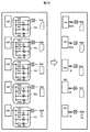
図16は、図8に示す駆動電極を駆動する場合の時定数調整回路の状態とその等価回路とを示す図である。図16において、左側には、各駆動電極に対する時定数調整回路TCCのスイッチ素子SWa、SWb、SWc、SWdのオン状態およびオフ状態が示される。また、図16において、右側には、各駆動電極に対する時定数調整回路TCCによって付加される時定数の等価回路が示される。なお、以下では、抵抗素子Rb、Rc、Rdの値を同一の値Rと考えた場合について説明する。
表示パネルPNLの4つのコーナーに設けられた駆動電極SxCに対応する時定数調整回路TCCにおいて、スイッチ素子SWa、SWb、SWc、SWdは、オフ状態、オン状態、オン状態、オン状態にされる。したがって、この場合、時定数調整回路TCCによって、R/3の時定数が付加される。
ホール部HOLの周りに設けられた4つの駆動電極SxHに対応する時定数調整回路TCCにおいて、スイッチ素子SWa、SWb、SWc、SWdは、オフ状態、オフ状態、オン状態、オン状態にされる。したがって、この場合、時定数調整回路TCCによって、R/2の時定数が付加される。
通常の駆動電極Sxnに対応する時定数調整回路TCCにおいて、スイッチ素子SWa、SWb、SWc、SWdは、オン状態、オフ状態、オフ状態、オフ状態にされる。したがって、この場合、時定数調整回路TCCによって、時定数が付加されない(0)。
ノッチ部NTCに設けられた2つの駆動電極SxNに対応する時定数調整回路TCCにおいて、スイッチ素子SWa、SWb、SWc、SWdは、オフ状態、オン状態、オフ状態、オフ状態にされる。したがって、この場合、時定数調整回路TCCによって、Rの時定数が付加される。
図13および図16では、図8に示す様に、面積の異なる4つの駆動電極(SxN、SxN、SxC、Sxn)が表示パネルPNLに存在することを前提として、時定数調整回路TCCが4種類の時定数(0、R、R/2、R/3)を調整可能に構成されている。表示パネルPNLに面積の異なるN個の駆動電極が存在する場合、時定数調整回路TCCは、N種類の時定数を調整可能に構成すればよい。また、異なるN個の駆動電極の面積あるいは面積比に応じて、時定数が略同一に設定できるように、抵抗素子Rb、Rc、Rdの値は異なる値としてもよい。
実施態様によれば、次の1または複数の効果を得ることができる。
1)駆動電極の面積に応じて、時定数調整回路TCCによって付加される時定数を調整することにより、ブロック状に見えてしまうことを防止できる。したがって、表示パネルの表示品質を向上させることができる。
2)駆動電極の面積に応じて、時定数調整回路TCCによって付加される時定数を調整することにより、タッチ検出の誤判定を起こす可能性を低減することができる。
3)時定数調整回路TCCは、表示パネルPNLに設けられたすべての駆動電極に対応する駆動回路(IOC)に設けた。そのため、表示パネルPNLに設けられる、ノッチ部NTCの個数および配置位置、ホール部HOLの個数および配置位置に柔軟に対応することが可能である。
(変形例)
次に、いくつかの変形例を説明する。
次に、いくつかの変形例を説明する。
(変形例1)
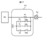
図17は、変形例1に係る時定数調整回路を示す図である。図13に示す時定数調整回路TCCは、抵抗素子Rb、Rc、Rdによって、時定数を調整した。図17の時定数調整回路TCCでは、複数の容量素子Cb、Cc、Cdによって、時定数を調整する。容量素子Cb、Cc、Cdは、スイッチ素子SWb、SWc、SWdのそれぞれのオン状態およびオフ状態を制御することにより、入出力回路IOCと外部端子Texとの間における容量値が時定数調整回路TCCによって調整できる。これにより、入出力回路IOCと駆動電極Sx11との間における時定数の調整を行うことが可能である。
図17は、変形例1に係る時定数調整回路を示す図である。図13に示す時定数調整回路TCCは、抵抗素子Rb、Rc、Rdによって、時定数を調整した。図17の時定数調整回路TCCでは、複数の容量素子Cb、Cc、Cdによって、時定数を調整する。容量素子Cb、Cc、Cdは、スイッチ素子SWb、SWc、SWdのそれぞれのオン状態およびオフ状態を制御することにより、入出力回路IOCと外部端子Texとの間における容量値が時定数調整回路TCCによって調整できる。これにより、入出力回路IOCと駆動電極Sx11との間における時定数の調整を行うことが可能である。
(変形例2)
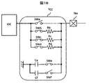
図18は、変形例2に係る時定数調整回路を示す図である。図18に示される時定数調整回路TCCには、図13に示された複数のスイッチ素子SWa、SWb、SWc、SWdおよび複数の抵抗素子Rb、Rc、Rdに追加して、図17で示したようなスイッチ素子SWe、SWfおよび容量素子Ce、Cfが設けられる。つまり、スイッチ素子SWa、SWb、SWc、SWd、SWe、SWfのそれぞれのオン状態およびオフ状態を制御することにより、抵抗素子(Rb、Rc、Rd)による時定数と容量素子(Ce、Cf)による時定数とを調整することが可能である。
図18は、変形例2に係る時定数調整回路を示す図である。図18に示される時定数調整回路TCCには、図13に示された複数のスイッチ素子SWa、SWb、SWc、SWdおよび複数の抵抗素子Rb、Rc、Rdに追加して、図17で示したようなスイッチ素子SWe、SWfおよび容量素子Ce、Cfが設けられる。つまり、スイッチ素子SWa、SWb、SWc、SWd、SWe、SWfのそれぞれのオン状態およびオフ状態を制御することにより、抵抗素子(Rb、Rc、Rd)による時定数と容量素子(Ce、Cf)による時定数とを調整することが可能である。
(変形例3)
図16に示す構成では、表示パネルPNLに設けられたすべての駆動電極に対して時定数調整回路TCCを設けた構成例を示した。しかしながら、すべての駆動電極に対して時定数調整回路TCCを設けると、表示制御装置DIのチップ面積が増加してしまうと考えられる。変形例3では、特定の駆動電極に対してのみ時定数調整回路TCCを設ける構成例を説明する。
図16に示す構成では、表示パネルPNLに設けられたすべての駆動電極に対して時定数調整回路TCCを設けた構成例を示した。しかしながら、すべての駆動電極に対して時定数調整回路TCCを設けると、表示制御装置DIのチップ面積が増加してしまうと考えられる。変形例3では、特定の駆動電極に対してのみ時定数調整回路TCCを設ける構成例を説明する。
図19は、表示パネルPNLの上部側に1つのノッチ部NTCが設けられた場合の駆動電極の平面図である。図20は、表示パネルPNLの上部側に1つのホール部HOLが設けられた場合の駆動電極の平面図である。図19および図20からわかるように、ノッチ部NTCやホール部HOLは、表示パネルPNLの上部側に設けられることが多い。言い方を変えれば、ノッチ部NTCやホール部HOLは、表示パネルPNLをY方向に、たとえば、5等分した場合において、上方の1/5の領域に主に設けられる可能性が高く、下方の4/5の領域には設けられない可能性が高い。
また、表示パネルPNLの4つのコーナー部に位置する駆動電極SxCは、表示パネルPNLの外形に合わせて、駆動電極Sxnの面積と比較して、面積の少ない駆動電極とされる可能性が高い。
したがって、図19および図20において、網掛けで示される駆動電極(表示パネルPNLの上方の1/5の領域に設けられる駆動電極、および、下方の2つコーナー部の駆動電極SxC)に対して、時定数制御回路TCCを付加し、それ以外の網掛けのない白色の駆動電極に対しては、時定数制御回路TCCを付加しない構成とすることができる。
図21は、網掛けで示される駆動電極およびそれ以外の駆動電極に対する回路構成を示す図である。図21に示す様に、網掛けで示される駆動電極(表示パネルPNLの上方の1/5の領域に設けられる駆動電極(SxC、Sxn、SxNまたはSxH)、および、下方の2つコーナー部の駆動電極(SxC))に対しては、時定数制御回路TCCが設けられる。一方、それ以外の網掛けのない白色の駆動電極(Sxn)に対しては、時定数制御回路TCCが付加されていない。時定数制御回路TCCは、図13、図17または図18に示す時定数制御回路TCCを利用することが可能である。
したがって、図16と比較して、表示制御装置DIに設けられる時定数調整回路TCCの数をほぼ1/5にできるので、表示制御装置DIのチップ面積の増加を低減することができる。
この場合、さらに、表示制御装置DIに設けられる時定数調整回路TCCを制御するレジスタREGのビット数も、図16と比較して、ほぼ1/5にできる。したがって、命令によるレジスタREGへの制御データのセット動作も、短時間に行うことができる。
さらに、ノッチ部NTCやホール部HOLは、表示パネルPNLの上方の1/5の領域内において、配置位置や個数を任意に決定できるので、表示パネルPNLの設計の自由度を妨げることもない。
変形例3では、表示パネルPNLの上方の1/5の領域としたが、これに限定されない。少なくとも4つのコーナー部の駆動電極(SxC)と、ノッチ部NTCやホール部HOLが形成されると予想される領域内の駆動電極に対して、時定数調整回路TCCによって時定数を付加できるようにすればよい。
本発明の実施の形態として上述した表示装置を基にして、当業者が適宜設計変更して実施し得る全ての表示装置も、本発明の要旨を包含する限り、本発明の範囲に属する。
本発明の思想の範疇において、当業者であれば、各種の変更例及び修正例に想到し得るものであり、それら変更例及び修正例についても本発明の範囲に属するものと了解される。例えば、上述の各実施形態に対して、当業者が適宜、構成要素の追加、削除もしくは設計変更を行ったもの、又は、工程の追加、省略若しくは条件変更を行ったものも、本発明の要旨を備えている限り、本発明の範囲に含まれる。
また、本実施形態において述べた態様によりもたらされる他の作用効果について本明細書記載から明らかなもの、又は当業者において適宜想到し得るものについては、当然に本発明によりもたらされるものと解される。
上記実施形態に開示されている複数の構成要素の適宜な組み合せにより種々の発明を形成できる。例えば、実施形態に示される全構成要素から幾つかの構成要素を削除してもよい。更に、異なる実施形態に亘る構成要素を適宜組み合せてもよい。
DSP:表示装置
PNL:表示パネル
DI:表示制御装置
IOC:入出力回路
AMP1、AMP2:駆動回路
DET:検出回路
NTC:ノッチ部
HOL:ホール部
Sx、SxN、SxH、SxC、Sxn:駆動電極
TCC:時定数調整回路
Rb、Rc、Rd:抵抗素子
SWa、SWb、SWc、SWd:スイッチ素子
Cb、Cc、Cd、Ce、Cf:容量素子
REG:レジスタ
PNL:表示パネル
DI:表示制御装置
IOC:入出力回路
AMP1、AMP2:駆動回路
DET:検出回路
NTC:ノッチ部
HOL:ホール部
Sx、SxN、SxH、SxC、Sxn:駆動電極
TCC:時定数調整回路
Rb、Rc、Rd:抵抗素子
SWa、SWb、SWc、SWd:スイッチ素子
Cb、Cc、Cd、Ce、Cf:容量素子
REG:レジスタ
Claims (8)
- 複数の駆動回路と、
前記複数の駆動回路の出力に各々接続される複数の駆動電極と、を含み、
前記複数の駆動電極内の少なくとも1つの駆動電極の面積は、他より小さく、
面積が小さい前記少なくとも1つの駆動電極に対応する駆動回路の出力の時定数を調整するための時定数調整回路を有する、
表示装置。 - 前記時定数調整回路による時定数の調整は、抵抗の切り替えにより行われる、請求項1に記載の表示装置。
- 前記時定数調整回路による時定数の調整は、容量の切り替えにより行われる、請求項1に記載の表示装置。
- 前記複数の駆動電極と対向した複数の画素電極を有し、
前記複数の駆動電極と前記複数の画素電極との間に液晶層を有し、
表示期間において、前記複数の駆動電極と前記複数の画素電極との間に所定の電圧が印加され、
前記表示期間と異なるタッチ検出期間において、前記複数の駆動電極に外部近接物体を検出するための交流電圧が印加される、請求項1に記載の表示装置。 - 前記複数の駆動電極は、マトリクス状に配置され、
前記複数の駆動電極は、セルフ検出により駆動される、請求項4に記載の表示装置。 - 前記複数の駆動電極に対向する複数の検出電極を含み、
前記複数の駆動電極と前記複数の検出電極は、ミューチャル検出により駆動される、請求項4に記載の表示装置。 - レジスタを含み、
前記時定数の調整は、前記レジスタへの設定によって行われる、請求項1に記載の表示装置。 - 前記複数の駆動電極を含み、平面視において、矩形形状の表示パネルを有し、
面積が小さい前記少なくとも1つの駆動電極は、
前記表示パネルの4つの角部に配置される駆動電極、および、前記表示パネルの上部の1/5より上に配置される駆動電極の内の少なくとも1つの駆動電極である、請求項1に記載の表示装置。
Applications Claiming Priority (2)
| Application Number | Priority Date | Filing Date | Title |
|---|---|---|---|
| JP2018233197A JP7250500B2 (ja) | 2018-12-13 | 2018-12-13 | 表示装置 |
| JP2018-233197 | 2018-12-13 |
Publications (1)
| Publication Number | Publication Date |
|---|---|
| WO2020121762A1 true WO2020121762A1 (ja) | 2020-06-18 |
Family
ID=71076990
Family Applications (1)
| Application Number | Title | Priority Date | Filing Date |
|---|---|---|---|
| PCT/JP2019/045413 Ceased WO2020121762A1 (ja) | 2018-12-13 | 2019-11-20 | 表示装置 |
Country Status (2)
| Country | Link |
|---|---|
| JP (2) | JP7250500B2 (ja) |
| WO (1) | WO2020121762A1 (ja) |
Cited By (1)
| Publication number | Priority date | Publication date | Assignee | Title |
|---|---|---|---|---|
| CN115412082A (zh) * | 2021-05-26 | 2022-11-29 | 夏普株式会社 | 触摸面板装置 |
Families Citing this family (1)
| Publication number | Priority date | Publication date | Assignee | Title |
|---|---|---|---|---|
| US12052484B2 (en) * | 2021-04-27 | 2024-07-30 | Apple Inc. | Camera integration for portable electronic devices |
Citations (4)
| Publication number | Priority date | Publication date | Assignee | Title |
|---|---|---|---|---|
| JP2014106864A (ja) * | 2012-11-29 | 2014-06-09 | Renesas Sp Drivers Inc | 半導体装置及び電子機器 |
| WO2015182473A1 (ja) * | 2014-05-28 | 2015-12-03 | シャープ株式会社 | タッチパネル装置 |
| JP2016110643A (ja) * | 2014-12-01 | 2016-06-20 | 株式会社半導体エネルギー研究所 | タッチパネル |
| JP2017182146A (ja) * | 2016-03-28 | 2017-10-05 | 株式会社ジャパンディスプレイ | センサ及びセンサ付き表示装置 |
Family Cites Families (4)
| Publication number | Priority date | Publication date | Assignee | Title |
|---|---|---|---|---|
| JPH03107188A (ja) * | 1989-09-20 | 1991-05-07 | Olympus Optical Co Ltd | El表示装置 |
| US8941640B2 (en) | 2012-06-08 | 2015-01-27 | Apple Inc. | Differential VCOM resistance or capacitance tuning for improved image quality |
| CN108228004B (zh) * | 2018-03-23 | 2022-10-04 | 上海中航光电子有限公司 | 显示面板以及显示装置 |
| CN108984037B (zh) * | 2018-07-24 | 2020-04-07 | 武汉华星光电技术有限公司 | 触控显示面板的驱动方法 |
-
2018
- 2018-12-13 JP JP2018233197A patent/JP7250500B2/ja active Active
-
2019
- 2019-11-20 WO PCT/JP2019/045413 patent/WO2020121762A1/ja not_active Ceased
-
2023
- 2023-03-22 JP JP2023044906A patent/JP2023076515A/ja active Pending
Patent Citations (4)
| Publication number | Priority date | Publication date | Assignee | Title |
|---|---|---|---|---|
| JP2014106864A (ja) * | 2012-11-29 | 2014-06-09 | Renesas Sp Drivers Inc | 半導体装置及び電子機器 |
| WO2015182473A1 (ja) * | 2014-05-28 | 2015-12-03 | シャープ株式会社 | タッチパネル装置 |
| JP2016110643A (ja) * | 2014-12-01 | 2016-06-20 | 株式会社半導体エネルギー研究所 | タッチパネル |
| JP2017182146A (ja) * | 2016-03-28 | 2017-10-05 | 株式会社ジャパンディスプレイ | センサ及びセンサ付き表示装置 |
Cited By (2)
| Publication number | Priority date | Publication date | Assignee | Title |
|---|---|---|---|---|
| CN115412082A (zh) * | 2021-05-26 | 2022-11-29 | 夏普株式会社 | 触摸面板装置 |
| CN115412082B (zh) * | 2021-05-26 | 2025-10-10 | 夏普株式会社 | 触摸面板装置 |
Also Published As
| Publication number | Publication date |
|---|---|
| JP2023076515A (ja) | 2023-06-01 |
| JP2020095491A (ja) | 2020-06-18 |
| JP7250500B2 (ja) | 2023-04-03 |
Similar Documents
| Publication | Publication Date | Title |
|---|---|---|
| US10503296B2 (en) | Touch display panel and display device | |
| EP2698689B1 (en) | In-cell touch panel | |
| US20190121491A1 (en) | Display device | |
| US11175784B2 (en) | Touch panel driving circuit | |
| JP6840554B2 (ja) | 検出装置及び表示装置 | |
| US11703968B2 (en) | Display device and circuit board | |
| US11112916B2 (en) | Display device including detection device | |
| US10372251B2 (en) | Display device | |
| US8766892B2 (en) | Display device with display panel having sensors therein | |
| JP7466030B2 (ja) | 表示装置 | |
| US20180284922A1 (en) | Display device | |
| US20150153767A1 (en) | Display device | |
| JP2023076515A (ja) | 表示装置 | |
| JP7466015B2 (ja) | 表示装置 | |
| KR20170080314A (ko) | 터치패널이 내장된 표시장치 | |
| JP2017146438A (ja) | 液晶表示装置 | |
| US10976581B2 (en) | Display device | |
| WO2019203362A1 (ja) | 表示装置 |
Legal Events
| Date | Code | Title | Description |
|---|---|---|---|
| 121 | Ep: the epo has been informed by wipo that ep was designated in this application |
Ref document number: 19896208 Country of ref document: EP Kind code of ref document: A1 |
|
| NENP | Non-entry into the national phase |
Ref country code: DE |
|
| 122 | Ep: pct application non-entry in european phase |
Ref document number: 19896208 Country of ref document: EP Kind code of ref document: A1 |