WO2020116409A1 - グランド部材及びシールドプリント配線板 - Google Patents
グランド部材及びシールドプリント配線板 Download PDFInfo
- Publication number
- WO2020116409A1 WO2020116409A1 PCT/JP2019/047104 JP2019047104W WO2020116409A1 WO 2020116409 A1 WO2020116409 A1 WO 2020116409A1 JP 2019047104 W JP2019047104 W JP 2019047104W WO 2020116409 A1 WO2020116409 A1 WO 2020116409A1
- Authority
- WO
- WIPO (PCT)
- Prior art keywords
- ground member
- layer
- wiring board
- printed wiring
- conductive
- Prior art date
- Legal status (The legal status is an assumption and is not a legal conclusion. Google has not performed a legal analysis and makes no representation as to the accuracy of the status listed.)
- Ceased
Links
Images











Classifications
-
- H—ELECTRICITY
- H05—ELECTRIC TECHNIQUES NOT OTHERWISE PROVIDED FOR
- H05K—PRINTED CIRCUITS; CASINGS OR CONSTRUCTIONAL DETAILS OF ELECTRIC APPARATUS; MANUFACTURE OF ASSEMBLAGES OF ELECTRICAL COMPONENTS
- H05K1/00—Printed circuits
- H05K1/02—Details
- H05K1/0213—Electrical arrangements not otherwise provided for
- H05K1/0216—Reduction of cross-talk, noise or electromagnetic interference
- H05K1/0218—Reduction of cross-talk, noise or electromagnetic interference by printed shielding conductors, ground planes or power plane
-
- H—ELECTRICITY
- H05—ELECTRIC TECHNIQUES NOT OTHERWISE PROVIDED FOR
- H05K—PRINTED CIRCUITS; CASINGS OR CONSTRUCTIONAL DETAILS OF ELECTRIC APPARATUS; MANUFACTURE OF ASSEMBLAGES OF ELECTRICAL COMPONENTS
- H05K1/00—Printed circuits
- H05K1/02—Details
- H05K1/0213—Electrical arrangements not otherwise provided for
- H05K1/0216—Reduction of cross-talk, noise or electromagnetic interference
-
- H—ELECTRICITY
- H05—ELECTRIC TECHNIQUES NOT OTHERWISE PROVIDED FOR
- H05K—PRINTED CIRCUITS; CASINGS OR CONSTRUCTIONAL DETAILS OF ELECTRIC APPARATUS; MANUFACTURE OF ASSEMBLAGES OF ELECTRICAL COMPONENTS
- H05K1/00—Printed circuits
- H05K1/02—Details
- H05K1/09—Use of materials for the conductive, e.g. metallic pattern
-
- H—ELECTRICITY
- H05—ELECTRIC TECHNIQUES NOT OTHERWISE PROVIDED FOR
- H05K—PRINTED CIRCUITS; CASINGS OR CONSTRUCTIONAL DETAILS OF ELECTRIC APPARATUS; MANUFACTURE OF ASSEMBLAGES OF ELECTRICAL COMPONENTS
- H05K3/00—Apparatus or processes for manufacturing printed circuits
- H05K3/22—Secondary treatment of printed circuits
- H05K3/28—Applying non-metallic protective coatings
-
- H—ELECTRICITY
- H05—ELECTRIC TECHNIQUES NOT OTHERWISE PROVIDED FOR
- H05K—PRINTED CIRCUITS; CASINGS OR CONSTRUCTIONAL DETAILS OF ELECTRIC APPARATUS; MANUFACTURE OF ASSEMBLAGES OF ELECTRICAL COMPONENTS
- H05K9/00—Screening of apparatus or components against electric or magnetic fields
- H05K9/0064—Earth or grounding circuit
-
- H—ELECTRICITY
- H05—ELECTRIC TECHNIQUES NOT OTHERWISE PROVIDED FOR
- H05K—PRINTED CIRCUITS; CASINGS OR CONSTRUCTIONAL DETAILS OF ELECTRIC APPARATUS; MANUFACTURE OF ASSEMBLAGES OF ELECTRICAL COMPONENTS
- H05K9/00—Screening of apparatus or components against electric or magnetic fields
- H05K9/0073—Shielding materials
- H05K9/0081—Electromagnetic shielding materials, e.g. EMI, RFI shielding
-
- H—ELECTRICITY
- H05—ELECTRIC TECHNIQUES NOT OTHERWISE PROVIDED FOR
- H05K—PRINTED CIRCUITS; CASINGS OR CONSTRUCTIONAL DETAILS OF ELECTRIC APPARATUS; MANUFACTURE OF ASSEMBLAGES OF ELECTRICAL COMPONENTS
- H05K1/00—Printed circuits
- H05K1/02—Details
- H05K1/0213—Electrical arrangements not otherwise provided for
- H05K1/0215—Grounding of printed circuits by connection to external grounding means
-
- H—ELECTRICITY
- H05—ELECTRIC TECHNIQUES NOT OTHERWISE PROVIDED FOR
- H05K—PRINTED CIRCUITS; CASINGS OR CONSTRUCTIONAL DETAILS OF ELECTRIC APPARATUS; MANUFACTURE OF ASSEMBLAGES OF ELECTRICAL COMPONENTS
- H05K2201/00—Indexing scheme relating to printed circuits covered by H05K1/00
- H05K2201/07—Electric details
- H05K2201/0707—Shielding
- H05K2201/0715—Shielding provided by an outer layer of PCB
Definitions
- the present invention relates to a ground member and a shield printed wiring board.
- Printed wiring boards are widely used in electronic devices such as mobile phones, video cameras, and notebook computers to incorporate circuits in their mechanisms. It is also used to connect a movable part such as a printer head and a control part. In these electronic devices, electromagnetic wave shielding measures are indispensable, and shielded printed wiring boards having electromagnetic wave shielding measures are also used in printed wiring boards used in devices.
- an electromagnetic wave shield measure a method of covering a printed wiring board with a conductive shield layer is known.
- a method of electrically connecting a ground circuit of a printed wiring board and an external ground via a shield layer is also known as a measure against noise.
- Patent Document 1 discloses a shielded printed wiring board further including an external ground member for ensuring electrical connection between the ground circuit of the printed circuit and the external ground.
- Patent Document 1 includes a printed wiring board and an electromagnetic wave shield layer that covers at least a part of the wiring of the printed wiring board, is electrically connected to a ground circuit of the printed wiring board, and is externally grounded. Further comprising an external ground member electrically connected to the member, the electromagnetic wave shield layer is electrically connected to the ground circuit of the printed wiring board and the external ground member, a part of the external ground member , Existing between the printed wiring board and the electromagnetic wave shield layer, another part of the external ground member, one surface is placed on the printed wiring board, the other surface is An exposed, shielded printed wiring board is disclosed.
- the external ground member (ground member) described in Patent Document 1 includes a metal foil (conductive layer) and an adhesive layer provided on one surface of the metal foil.
- the printed wiring board described in Patent Document 1 has a configuration in which the print pattern on the base film is covered with an insulating film (coverlay).
- the ground member When manufacturing a shielded printed wiring board using such a ground member, first, the ground member is arranged on the printed wiring board so that the adhesive layer of the ground member contacts the printed wiring board. After that, the ground member is bonded and fixed to the printed wiring board by hot pressing.
- electronic components will be further mounted on the shielded printed wiring board provided with such a ground member.
- solder is used, but when the electronic components are mounted by solder reflow, the shield printed wiring board is heated.
- the adhesive layer of the ground member or the cover lay of the printed wiring board, etc. The gas is generated from.
- the base film of the printed wiring board is made of a highly hygroscopic resin such as polyimide, steam may be generated from the base film by heating.
- These volatile components generated from the adhesive layer of the ground member, the coverlay, and the base film cannot pass through the conductive layer of the ground member, and therefore accumulate between the conductive layer and the adhesive layer. Therefore, if the heating is further rapidly performed thereafter, the volatile components accumulated between the conductive layer of the ground member and the adhesive layer expand, and the interlayer adhesion between the conductive layer of the ground member and the adhesive layer is destroyed. There was a problem.
- the ground member of the present invention is a ground member including a conductive layer and an adhesive layer laminated on the conductive layer, the adhesive layer having a binder component and hard particles, the adhesive layer Is characterized by having a thickness of 5 to 30 ⁇ m.
- the ground member of the present invention will be used for manufacturing a shield printed wiring board. That is, when the shielded printed wiring board is manufactured, the ground member of the present invention is arranged on the printed wiring board so that the adhesive layer contacts the cover lay of the printed wiring board. After that, the ground member is bonded and fixed to the printed wiring board by hot pressing.
- the hard particles contained in the adhesive layer of the ground member of the present invention press the conductive layer of the ground member in this hot press to form holes or depressions in the conductive layer through which volatile components can pass. Therefore, even if a volatile component is generated by heating in the process of manufacturing the shield printed wiring board, the volatile component can pass through the conductive layer.
- the volatile component passes through the conductive layer. be able to. That is, it is possible to prevent volatile components from accumulating between the conductive layer and the adhesive layer of the ground member, and as a result, due to heating during manufacturing of the shield printed wiring board or mounting of electronic components on the shield printed wiring board, It is possible to prevent the interlayer adhesion between the conductive layer and the adhesive layer of the ground member from being destroyed.
- the thickness of the adhesive layer is 5 to 30 ⁇ m. If the thickness of the adhesive layer is less than 5 ⁇ m, the adhesive strength will be insufficient. When the thickness of the adhesive layer is more than 30 ⁇ m, the pressure that the hard particles press against the conductive layer at the time of hot pressing is dispersed, and it is not possible to form holes or depressions in the conductive layer through which volatile components can pass.
- the Mohs hardness of the hard particles is preferably 1.5 times or more the Mohs hardness of the conductive layer.
- the Mohs hardness of the hard particles is 1.5 times or more the Mohs hardness of the conductive layer, the hard particles are easily embedded in the conductive layer during hot pressing. As a result, it becomes easy to form holes or depressions through which volatile components can pass in the conductive layer.
- the hard particles have a Mohs hardness of 4 to 7.
- Mohs hardness of the hard particles is 4 to 7, it becomes easy to form holes or depressions through which the volatile components can pass in the conductive layer without crushing the hard particles during hot pressing.
- the average particle size of the hard particles is preferably 2.5 to 25 ⁇ m.
- the average particle diameter of the hard particles is within this range, it is possible to suitably form holes or depressions through which the volatile component can pass in the conductive layer during hot pressing.
- the average particle diameter of the hard particles is less than 2.5 ⁇ m, it is difficult to form sufficiently large holes or depressions in the conductive layer during hot pressing, and it becomes difficult for volatile components to pass through the conductive layer.
- the average particle diameter of the hard particles exceeds 25 ⁇ m, the holes and dents formed in the conductive layer become large during hot pressing, and the strength of the conductive layer tends to decrease.
- the hard particles are preferably made of silica.
- Silica has a sufficiently high Mohs hardness and suitably functions as hard particles.
- the conductive layer is preferably made of at least one selected from the group consisting of copper, silver, gold and nickel.
- the conductive layer of the ground member is electrically connected to the ground circuit of the printed wiring board. Further, in the shield printed wiring board using the ground member of the present invention, the conductive layer is connected to the external ground.
- the conductive layer of the ground member is made of at least one selected from the group consisting of copper, silver, gold and nickel, these materials have excellent conductivity, so that the electric resistance value between the ground circuit and the external ground is lowered. be able to.
- the adhesive layer further has conductive particles.
- the adhesive layer functions as a conductive adhesive layer.
- the average particle size of the hard particles is preferably smaller than the average particle size of the conductive particles.
- the average particle diameter of the hard particles is larger than the average particle diameter of the conductive particles, the hard particles are easily exposed from the adhesive layer of the ground member. Therefore, the adhesiveness of the adhesive layer is likely to be lost.
- the Mohs hardness of the hard particles is preferably higher than the Mohs hardness of the conductive particles. If the Mohs hardness of the hard particles is higher than the Mohs hardness of the conductive particles, even if the adherend of the ground member of the present invention is soft, it becomes easy to form holes or depressions through which volatile components can pass in the conductive layer. ..
- the thickness of the binder component in the adhesive layer is preferably smaller than the average particle diameter of the conductive particles.
- the ground member of the present invention may be arranged in an electromagnetic wave shielding film including a protective layer and a shield layer laminated on the protective layer.
- the adhesive layer of the ground member is arranged so as to be in contact with the protective layer of the electromagnetic wave shielding film, and the conductive particles of the ground member are arranged so as to penetrate through the protective layer of the electromagnetic wave shielding film.
- the conductive particles reliably penetrate the protective layer of the electromagnetic wave shielding film, and the conductive particles Can be brought into contact with the shield layer of the electromagnetic wave shielding film.
- the ground member of the present invention is arranged so that the adhesive layer is in contact with the protective layer with respect to the electromagnetic wave shielding film having a protective layer and a shield layer laminated on the protective layer, and the conductive particles are You may arrange
- the conductive layer of the ground member of the present invention is connected to the external ground, and the shield layer of the electromagnetic wave shielding film is electrically connected to the ground circuit of the printed wiring board.
- the conductive particles of the ground member of the present invention penetrate the protective layer of the electromagnetic wave shielding film and come into contact with the shield layer of the electromagnetic wave shielding film. As described above, by using the ground member of the present invention, it is possible to electrically connect the ground circuit of the printed wiring board using the electromagnetic wave shielding film and the external ground.
- the ground member of the present invention is a base film, a printed circuit including a ground circuit arranged on the base film, and a printed wiring board composed of a cover lay covering the printed circuit, and arranged on the cover lay.
- the ground member may be arranged such that the adhesive layer is in contact with the protective layer, and that the conductive particles penetrate the protective layer.
- the conductive layer of the ground member of the present invention is electrically connected to the external ground. The conductive particles of the ground member penetrate the protective layer of the shield printed wiring board and come into contact with the shield layer. As described above, by using the ground member of the present invention, the ground circuit of the shield printed wiring board and the external ground can be electrically connected.
- the adhesive layer may have insulating properties, and conductive bumps may be formed on the conductive layer on the adhesive layer side.
- the conductive layer and the adherend can be electrically connected via the conductive bumps.
- the shielded printed wiring board of the present invention comprises a printed wiring board comprising a base film, a printed circuit including a ground circuit arranged on the base film, and a coverlay covering the printed circuit, and a printed wiring board on the coverlay.
- a shield printed wiring board that is disposed and that includes a shield layer electrically connected to the ground circuit, wherein the shield printed wiring board further includes the ground member of the present invention, and the cover member has the ground member.
- the ground member is arranged so that the adhesive layer of 1 is in contact, and the conductive layer of the ground member and the shield layer are electrically connected.
- Another shielded printed wiring board of the present invention is a printed wiring board comprising a base film, a printed circuit including a ground circuit arranged on the base film, and a cover lay covering the printed circuit, and the cover.
- a conductive adhesive layer which is disposed on the lay, is composed of a shield layer laminated on the conductive adhesive layer, and the electromagnetic wave shielding film electrically connected to the conductive adhesive layer and the ground circuit.
- a shield printed wiring board comprising, wherein the shield printed wiring board further comprises the ground member of the present invention, the ground member is arranged so that the adhesive layer of the ground member is in contact with the cover lay. The conductive layer of the ground member and the conductive adhesive layer of the electromagnetic wave shielding film are electrically connected.
- Another shielded printed wiring board of the present invention is a printed wiring board comprising a base film, a printed circuit including a ground circuit arranged on the base film, and a coverlay covering the printed circuit, and a coverlay of the coverlay.
- a shielded printed wiring board comprising: a shield layer disposed above; electrically connected to the ground circuit; and a protective layer provided on a surface of the shield layer opposite to the printed circuit side.
- the shielded printed wiring board further comprises the ground member of the present invention, the adhesive layer of the ground member is in contact with the protective layer, the ground member is arranged, conductive particles of the ground member, It is characterized in that it penetrates through the protective layer and is electrically connected to the conductive layer of the ground member and the shield layer.
- Another shielded printed wiring board of the present invention is a printed wiring board comprising a base film, a printed circuit including a ground circuit arranged on the base film, and a cover lay covering the printed circuit, and the cover.
- a shielded printed wiring board comprising: a shield layer disposed on a ray and electrically connected to the ground circuit; and a protective layer provided on a surface of the shield layer opposite to the printed circuit side.
- the shield printed wiring board further includes the ground member of the present invention, the ground member is arranged so that the adhesive layer of the ground member is in contact with the protective layer, and the conductive bump of the ground member is provided. Is characterized in that it penetrates through the protective layer and is electrically connected to the conductive layer of the ground member and the shield layer.
- These shield printed wiring boards of the present invention include the ground member of the present invention. Therefore, it is possible to prevent the interlayer adhesion between the conductive layer and the adhesive layer of the ground member from being destroyed by heating during manufacturing of the shield printed wiring board or mounting of electronic components on the shield printed wiring board.
- the ground member of the present invention is used when manufacturing a shield printed wiring board.
- the hard particles contained in the adhesive layer of the ground member of the present invention press the conductive layer of the ground member, and the conductive layer has holes or depressions through which volatile components can pass. Will be formed. Therefore, even if a volatile component is generated by heating in the process of manufacturing the shield printed wiring board, the volatile component can pass through the conductive layer.
- FIG. 1 is a cross-sectional view schematically showing an example of the ground member according to the first embodiment of the present invention.
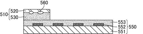
- FIG. 2A is a schematic diagram schematically showing an example of manufacturing a printed wiring board using a conventional ground member.
- FIG. 2B is a schematic diagram schematically showing an example of manufacturing a printed wiring board using a conventional ground member.
- FIG. 2C is a schematic diagram schematically showing an example of manufacturing a printed wiring board using a conventional ground member.
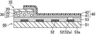
- FIG. 3A is a schematic diagram schematically showing an example of manufacturing a printed wiring board using the ground member according to the first embodiment of the present invention.
- FIG. 3B is a schematic view schematically showing an example of manufacturing a printed wiring board using the ground member according to the first embodiment of the present invention.
- FIG. 3A is a schematic diagram schematically showing an example of manufacturing a printed wiring board using the ground member according to the first embodiment of the present invention.
- FIG. 3B is a schematic view schematically showing an example of manufacturing a printed wiring board
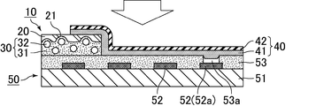
- FIG. 3C is a schematic diagram schematically showing an example of manufacturing a printed wiring board using the ground member according to the first embodiment of the present invention.
- FIG. 4 is a schematic view schematically showing an example of a printed wiring board preparing step of the method for manufacturing a shield printed wiring board using the ground member according to the first embodiment of the present invention.
- FIG. 5 is a schematic diagram which shows typically an example of the ground member arrangement process of the manufacturing method of the shield printed wiring board using the ground member which concerns on 1st Embodiment of this invention.
- FIG. 6 is a schematic view schematically showing an example of the electromagnetic wave shield film arranging step of the method for manufacturing a shield printed wiring board using the ground member according to the first embodiment of the present invention.
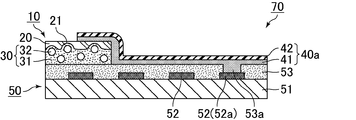
- FIG. 7A is a schematic view schematically showing an example of a hot pressing step in the method for manufacturing a shield printed wiring board using the ground member according to the first embodiment of the present invention.
- FIG. 7B is a schematic view schematically showing an example of the hot pressing step of the method for manufacturing a shield printed wiring board using the ground member according to the first embodiment of the present invention.
- FIG. 8 is a cross-sectional view schematically showing an example of the ground member according to the second embodiment of the present invention.
- FIG. 9A is a schematic view schematically showing how the ground member according to the second embodiment of the present invention is arranged on the electromagnetic wave shielding film.
- FIG. 9B is a schematic view schematically showing how the ground member according to the second embodiment of the present invention is arranged on the electromagnetic wave shielding film.
- FIG. 10A is a schematic view schematically showing how the ground member according to the second embodiment of the present invention is arranged on the shield printed wiring board.
- FIG. 10B is a schematic view schematically showing how the ground member according to the second embodiment of the present invention is arranged on the shield printed wiring board.
- FIG. 11 is a sectional view schematically showing an example of the ground member according to the third embodiment of the present invention.
- FIG. 12A is a schematic view schematically showing how the ground member according to the third embodiment of the present invention is arranged on the shield printed wiring board.
- FIG. 12B is a schematic view schematically showing how the ground member according to the third embodiment of the present invention is arranged on the shield printed wiring board.
- FIG. 13A is a schematic view schematically showing how the ground member according to the third embodiment of the present invention is arranged on the shield printed wiring board.
- FIG. 13B is a schematic view schematically showing how the ground member according to the third embodiment of the present invention is arranged on the shield printed wiring board.
- FIG. 13C is a schematic diagram schematically showing how the ground member according to the third embodiment of the present invention is arranged on the shield printed wiring board.
- FIG. 13D is a schematic view schematically showing how the ground member according to the third embodiment of the present invention is arranged on the shield printed wiring board.
- ground member of the present invention will be specifically described.
- the present invention is not limited to the following embodiments, and can be appropriately modified and applied without departing from the scope of the present invention.
- FIG. 1 is a cross-sectional view schematically showing an example of the ground member according to the first embodiment of the present invention.
- the ground member 10 includes a conductive layer 20 and an adhesive layer 30 laminated on the conductive layer 20. Further, the adhesive layer 30 has a binder component 31 and hard particles 32.
- the thickness T30 of the adhesive layer 30 is 5 to 30 ⁇ m.
- the ground member 10 will be used for manufacturing a shield printed wiring board.
- FIG. 2A, FIG. 2B, and FIG. 2C are schematic diagrams schematically showing an example of manufacturing a printed wiring board using a conventional ground member.
- a conventional ground member 510 including a conductive layer 520 and an adhesive layer 530 laminated on the conductive layer 520 has a printed circuit 552 formed on a base film 551 and the printed circuit 552 is covered by a cover layer.
- the printed wiring board 550 is covered with 553.
- the adhesive layer 530 of the conventional ground member 510 is arranged on the printed wiring board 550 side.
- the conventional ground member 510 is bonded and fixed to the printed wiring board 550.
- Electronic components will be further mounted on the printed wiring board 550 including the ground member 510. Solder is used when mounting the electronic component, but when mounting the electronic component by solder reflow, the printed wiring board 550 is heated.
- the volatile components accumulated between the conductive layer 520 and the adhesive layer 530 of the conventional ground member 510 expand, and the conventional ground member is expanded.
- the interlayer adhesion between the conductive layer 520 and the adhesive layer 530 of 510 may be destroyed.
- FIG. 3A, FIG. 3B, and FIG. 3C are schematic diagrams schematically showing an example of manufacturing a printed wiring board using the ground member according to the first embodiment of the present invention.
- the printed circuit 52 is formed on the base film 51, and the printed circuit 52 is the cover lay 53. It will be arranged on the covered printed wiring board 50. At this time, the adhesive layer 30 of the ground member 10 is arranged on the printed wiring board 50 side.
- the ground member 10 is bonded and fixed to the printed wiring board 50.
- the hard particles 32 contained in the adhesive layer 30 of the ground member 10 press the conductive layer 20 of the ground member 10 in this heating press, and the volatile component can pass through the conductive layer 20. Holes and depressions 21 will be formed.
- volatile components are generated when the ground member 10 is arranged on the printed wiring board 50 and heated and pressed, or when electronic components are mounted on the printed wiring board 50.
- such volatile components 60 can pass through the conductive layer 20 through the holes and the depressions 21. That is, it is possible to prevent the volatile component 60 from accumulating between the conductive layer 20 and the adhesive layer 30 of the ground member 10, and as a result, the interlayer adhesion between the conductive layer 20 and the adhesive layer 30 of the ground member 10 is destroyed. Can be prevented.
- ground member 10 Next, each structure of the ground member 10 will be described in detail.
- the material of the conductive layer 20 of the ground member 10 is not particularly limited and is preferably made of at least one selected from the group consisting of copper, silver, gold and nickel.
- the conductive layer 20 of the ground member 10 may be electrically connected to the ground circuit of the printed wiring board.
- the conductive layer 20 may be connected to the external ground.
- the conductive layer of the ground member 10 is made of at least one selected from the group consisting of copper, silver, gold, and nickel, these materials have excellent conductivity, so that the electric resistance value between the ground circuit and the external ground is low. can do.
- the conductive layer 20 preferably has a thickness of 1 to 9 ⁇ m, more preferably 2 to 7 ⁇ m. If the thickness of the conductive layer is less than 1 ⁇ m, the strength of the conductive layer becomes low and the conductive layer is easily damaged. When the thickness of the conductive layer is more than 9 ⁇ m, the conductive layer is too thick, and it is difficult for the hard particles to form pores or depressions through which volatile components can pass.
- the thickness T30 of the adhesive layer 30 is 5 to 30 ⁇ m. Further, the thickness T30 of the adhesive layer 30 is preferably 10 to 20 ⁇ m. If the thickness of the adhesive layer is less than 5 ⁇ m, the adhesive strength will be insufficient. When the thickness of the adhesive layer is more than 30 ⁇ m, the pressure that the hard particles press against the conductive layer at the time of hot pressing is dispersed, and it is not possible to form holes or depressions in the conductive layer through which volatile components can pass.
- the Mohs hardness of the hard particles 32 contained in the adhesive layer 30 is preferably 1.5 times or more, more preferably 1.6 to 2.3 times the Mohs hardness of the conductive layer 20. desirable.
- the Mohs hardness of the hard particles 32 is 1.5 times or more the Mohs hardness of the conductive layer 20, the hard particles 32 are easily embedded in the conductive layer 20 during hot pressing. As a result, it becomes easy to form holes or depressions 21 through which volatile components can pass in the conductive layer 20.
- the Mohs hardness of the hard particles 32 is preferably 4 to 7, and more preferably 5 to 7.
- the Mohs hardness of the hard particles 32 is 4 to 7, it becomes easy to form holes or depressions 21 through which volatile components can pass in the conductive layer 20 without crushing the hard particles 32 during hot pressing.
- the average particle diameter of the hard particles 32 is preferably 2.5 to 25 ⁇ m, more preferably 2.5 to 10 ⁇ m. When the average particle diameter of the hard particles 32 is in this range, it is possible to suitably form the holes and the depressions 21 through which the volatile components can pass in the conductive layer 20 during hot pressing. If the average particle diameter of the hard particles is less than 2.5 ⁇ m, it is difficult to form sufficiently large holes or depressions in the conductive layer during hot pressing, and it becomes difficult for volatile components to pass through the conductive layer. When the average particle diameter of the hard particles exceeds 25 ⁇ m, the holes and dents formed in the conductive layer become large during hot pressing, and the strength of the conductive layer tends to decrease.
- the hard particles 32 are preferably made of silica.
- Silica has a Mohs hardness of 7 and is sufficiently hard, so that it suitably functions as hard particles.
- the material of the binder component 31 constituting the adhesive layer 30 is not particularly limited, but a thermoplastic resin such as polystyrene-based, vinyl acetate-based, polyester-based, polyethylene-based, polypropylene-based, polyamide-based, rubber-based or acrylic-based resin, Thermosetting resins such as phenol, epoxy, urethane, urethane urea, melamine and alkyd can be used.
- a thermoplastic resin such as polystyrene-based, vinyl acetate-based, polyester-based, polyethylene-based, polypropylene-based, polyamide-based, rubber-based or acrylic-based resin
- Thermosetting resins such as phenol, epoxy, urethane, urethane urea, melamine and alkyd
- FIG. 4 is a schematic view schematically showing an example of a printed wiring board preparing step of the method for manufacturing a shield printed wiring board using the ground member according to the first embodiment of the present invention.
- FIG. 5 is a schematic diagram which shows typically an example of the ground member arrangement process of the manufacturing method of the shield printed wiring board using the ground member which concerns on 1st Embodiment of this invention.
- FIG. 6 is a schematic view schematically showing an example of the electromagnetic wave shield film arranging step of the method for manufacturing a shield printed wiring board using the ground member according to the first embodiment of the present invention.
- FIG. 7A and FIG. 7B are schematic views schematically showing an example of the hot pressing step of the method for manufacturing a shield printed wiring board using the ground member according to the first embodiment of the present invention.
- Printed Wiring Board Preparation Step As shown in FIG. 4, a base film 51, a printed circuit 52 including a ground circuit 52 a arranged on the base film 51, and a coverlay covering the printed circuit 52. A printed wiring board 50 composed of 53 is prepared. In the printed wiring board 50, a part of the ground circuit 52a is exposed by the opening 53a of the coverlay 53.
- the materials of the base film 51 and the coverlay 53 are preferably made of engineering plastic.
- engineering plastics include resins such as polyethylene terephthalate, polypropylene, crosslinked polyethylene, polyester, polybenzimidazole, polyimide, polyimideamide, polyetherimide, and polyphenylene sulfide.
- resins such as polyethylene terephthalate, polypropylene, crosslinked polyethylene, polyester, polybenzimidazole, polyimide, polyimideamide, polyetherimide, and polyphenylene sulfide.
- a polyphenylene sulfide film is preferable when flame retardancy is required, and a polyimide film is preferable when heat resistance is required.
- the base film 51 preferably has a thickness of 10 to 40 ⁇ m.
- the coverlay 53 preferably has a thickness of 10 to 50 ⁇ m.
- the material of the printed circuit 52 is not particularly limited, and may be a copper foil, a cured product of a conductive paste, or the like.
- the ground member 10 is arranged on the printed wiring board 50 so that the adhesive layer 30 of the ground member 10 contacts the cover lay 53 of the printed wiring board 50. ..
- an electromagnetic wave shield film 40 including a conductive adhesive layer 41 and a metal thin film 42 laminated on the conductive adhesive layer 41 is prepared. Then, the electromagnetic wave shielding film 40 is arranged on the printed wiring board 50 so that the conductive adhesive layer 41 of the electromagnetic wave shielding film 40 contacts the cover lay 53 of the printed wiring board 50 and a part of the ground member 10. At this time, after the hot pressing step described later, the conductive adhesive layer 41 of the electromagnetic wave shielding film 40 fills the opening 53a of the printed wiring board 50, and the conductive adhesive layer 41 of the electromagnetic wave shielding film 40 and the ground circuit 52a. The electromagnetic wave shielding film 40 is arranged so as to come into contact with. Further, after the hot pressing step described later, the electromagnetic wave shielding film 40 is arranged so that the conductive adhesive layer 41 of the electromagnetic wave shielding film 40 contacts the conductive layer 20 of the ground member 10.
- the conductive adhesive layer 41 of the electromagnetic wave shield film 40 is preferably made of conductive particles and resin.
- the conductive particles are not particularly limited, but at least one selected from the group consisting of copper powder, silver powder, nickel powder, silver-coated copper powder, gold-coated copper powder, silver-coated nickel powder and gold-coated nickel powder.
- the resin include a styrene resin composition, a vinyl acetate resin composition, a polyester resin composition, a polyethylene resin composition, a polypropylene resin composition, an imide resin composition, an amide resin composition, and an acrylic resin.
- a composition, a phenol resin composition, an epoxy resin composition, a urethane resin composition, a melamine resin composition, an alkyd resin composition, etc. can be used.
- the metal thin film 42 of the electromagnetic wave shield film 40 may include a layer made of a material such as gold, silver, copper, aluminum, nickel, tin, palladium, chromium, titanium, or zinc, and preferably includes a copper layer. Copper is a suitable material for the metal thin film 42 from the viewpoint of conductivity and economy.
- the metal thin film 42 may include a layer made of an alloy of the above metals. Further, as the metal thin film 42, a metal foil may be used, or a metal film formed by a method such as sputtering, electroless plating or electrolytic plating may be used.
- the electromagnetic wave shield film 40 after the hot pressing becomes the shield layer 40a.
- the hard particles 32 contained in the adhesive layer 30 of the ground member 10 push the conductive layer 20 of the ground member 10 to allow the volatile component to pass through the conductive layer 20.
- the depression 21 will be formed.
- volatile components are generated from the cover lay 53 of the printed wiring board 50 and the adhesive layer 30 of the ground member 10.
- volatile components can pass through the conductive layer 20 through the holes and the depressions 21. That is, it is possible to prevent the volatile component 60 from accumulating between the conductive layer 20 and the adhesive layer 30 of the ground member 10, and as a result, the interlayer adhesion between the conductive layer 20 and the adhesive layer 30 of the ground member 10 is destroyed. Can be prevented.
- the heating temperature in the hot pressing step is preferably 100 to 190°C, and more preferably 120 to 170°C.
- the pressing pressure in the hot pressing step is preferably 0.5 to 4.0 Pa, and more preferably 2.0 to 3.0 Pa.
- the shield printed wiring board 70 can be manufactured.
- Such a shield printed wiring board 70 is also the shield printed wiring board of the present invention. That is, as shown in FIG. 7B, the shield printed wiring board 70 includes the printed wiring board 50, the shield layer 40 a, and the ground member 10.
- the printed wiring board 50 includes a base film 51, a printed circuit 52 including a ground circuit 52 a arranged on the base film 51, and a coverlay 53 that covers the printed circuit 52. Further, the cover lay 53 is formed with an opening 53a exposing the ground circuit 52a.
- the shield layer 40 a includes a conductive adhesive layer 41 and a metal thin film 42 laminated on the conductive adhesive layer 41.
- the shield layer 40a is arranged on the printed wiring board 50 so that the conductive adhesive layer 41 contacts the cover lay 53.
- the conductive adhesive layer 41 fills the opening 53a of the cover lay 53 and is in contact with the ground circuit 52a.
- the ground member 10 includes a conductive layer 20 and an adhesive layer 30 laminated on the conductive layer 20.
- the ground member 10 is arranged on the printed wiring board 50 so that the adhesive layer 30 contacts the cover lay 53. Therefore, the conductive layer 20 of the ground member 10 and the shield layer 40a are electrically connected.
- the conductive adhesive layer 41 of the shield layer 40a is in contact with the ground circuit 52a, the conductive layer 20 of the ground member 10 and the ground circuit 52a are also electrically connected.
- the ground circuit 52a of the shield printed wiring board 70 and the external ground can be electrically connected.
- the shield layer may be composed of an insulating adhesive layer and a metal thin film laminated on the insulating adhesive layer.
- a plurality of conductive bumps are formed on the metal thin film on the side of the insulating adhesive layer, or the metal thin film has a projection shape, so that the conductive bump or the projection-shaped metal thin film and the ground circuit of the printed wiring board are formed.
- FIG. 8 is a cross-sectional view schematically showing an example of the ground member according to the second embodiment of the present invention.
- the ground member 110 shown in FIG. 8 has the same configuration as the ground member 10 except that the adhesive layer 130 has the conductive particles 133.
- the ground member 110 includes the conductive layer 120 and the adhesive layer 130 stacked on the conductive layer 120.
- the adhesive layer 130 includes the binder component 131, the hard particles 132, and the conductive particles 133.
- the thickness T130 of the adhesive layer 130 is 5 to 30 ⁇ m.
- the adhesive layer 130 functions as a conductive adhesive layer.
- the average particle size of the hard particles 132 is preferably smaller than the average particle size of the conductive particles 133.
- the average particle diameter of the hard particles 132 is larger than the average particle diameter of the conductive particles 133, the hard particles 132 are easily exposed from the adhesive layer 130 of the ground member 110. Therefore, the adhesiveness of the adhesive layer 130 is likely to be lost.
- the average particle size of the conductive particles 133 is preferably 8 to 25 ⁇ m, more preferably 10 to 25 ⁇ m.
- the Mohs hardness of the hard particles 132 is preferably higher than the Mohs hardness of the conductive particles 133, and more preferably 1.2 times or more the Mohs hardness of the conductive particles 133.
- the Mohs hardness of the hard particles 132 is higher than the Mohs hardness of the conductive particles 133, even if the adherend of the ground member 110 is soft, it is easy to form holes or depressions through which volatile components can pass in the conductive layer 120. Become.
- the Mohs hardness of the conductive particles 133 is preferably 5 to 9, and more preferably 6 to 7.
- the material of the conductive particles 133 is not particularly limited, but carbon, silver, copper, nickel, solder, aluminum, silver-coated copper filler obtained by silver-plating copper powder, and metal plating on resin balls, glass beads and the like.
- the applied filler or a mixture of these fillers may be mentioned.
- silver-coated copper filler or nickel which is relatively inexpensive and has excellent conductivity, is desirable.
- the ground member 110 may be disposed on an electromagnetic wave shield film including a protective layer and a shield layer laminated on the protective layer.
- 9A and 9B are schematic diagrams schematically showing how the ground member according to the second embodiment of the present invention is arranged on the electromagnetic wave shielding film.
- the electromagnetic wave shield film 180 on which the ground member 110 is arranged includes a protective layer 181 and a shield layer 182 laminated on the protective layer 181.
- the adhesive layer 130 of the ground member 110 is arranged so as to contact the protective layer 181 of the electromagnetic wave shielding film 180.
- the conductive particles 133 of the ground member 110 are pressed so as to penetrate the protective layer 181 of the electromagnetic wave shielding film 180.
- the hard particles 132 contained in the adhesive layer 130 of the ground member 110 form holes or depressions 121 in the conductive layer 120 through which volatile components can pass.
- the conductive layer 120 of the ground member 110 is connected to the external ground (not shown), and the shield layer 182 of the electromagnetic wave shielding film 180 is electrically connected to the ground circuit (not shown) of the printed wiring board. ..
- the ground member 110 it is possible to electrically connect the ground circuit of the printed wiring board using the electromagnetic wave shielding film and the external ground.
- the thickness of the binder component 131 in the adhesive layer 130 is preferably smaller than the average particle diameter of the conductive particles 133.
- the conductive particles 133 surely penetrate the protective layer 181 of the electromagnetic wave shielding film 180, and the conductive particles 133 and The electromagnetic wave shield film 180 can be brought into contact with the shield layer 182.
- the protective layer 181 and the shield layer 182 forming the electromagnetic wave shield film 180 may be conventional ones.
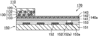
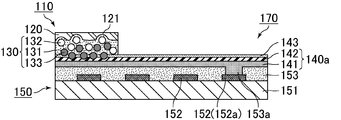
- the ground member 110 may be disposed on the shield printed wiring board.
- the case where the ground member 110 is arranged on the shield printed wiring board in this way will be described with reference to the drawings.
- 10A and 10B are schematic diagrams schematically showing how the ground member according to the second embodiment of the present invention is arranged on the shield printed wiring board.
- the shield printed wiring board 170 on which the ground member 110 is arranged covers the base film 151, the printed circuit 152 including the ground circuit 152 a arranged on the base film 151, and the printed circuit 152.
- the printed wiring board 150 includes a coverlay 153, a shield layer 140a formed on the coverlay 153, and a protective layer 143 formed on the shield layer 140a.
- An opening 153a exposing the ground circuit 152a is formed in the cover lay 153 of the printed wiring board 150.
- the shield layer 140a is composed of a conductive adhesive layer 141 and a metal thin film 142 laminated on the conductive adhesive layer 141. Further, the shield layer 140a is arranged on the printed wiring board 150 so that the conductive adhesive layer 141 is in contact with the cover lay 153. The conductive adhesive layer 141 fills the opening 153a of the cover lay 153 and is in contact with the ground circuit 152a.
- the ground member 110 is arranged on the shield printed wiring board 170 such that the adhesive layer 130 contacts the protective layer 143.
- the conductive particles 133 of the ground member 110 are pressurized so as to penetrate the protective layer 143. As a result, the conductive particles 133 come into contact with the metal thin film 142. At this time, the hard particles 132 contained in the adhesive layer 130 of the ground member 110 form holes or depressions 121 in the conductive layer 120 through which volatile components can pass.
- the conductive layer 120 of the ground member 110 will be connected to an external ground (not shown). In this way, by using the ground member 110, the ground circuit 152a of the shield printed wiring board 170 and the external ground can be electrically connected.
- the thickness of the binder component 131 in the adhesive layer 130 is preferably smaller than the average particle diameter of the conductive particles 133.
- the conductive particles 133 surely penetrate the protective layer 143, and the conductive particles 133 and the metal thin film 142 are formed. Can be contacted.
- Desirable materials for the base film 151, the printed circuit 152 (ground circuit 152a), the coverlay 153, the conductive adhesive layer 141, and the metal thin film 142 in the shield printed wiring board 170 are the base film 51 in the shield printed wiring board 70, It is the same as a desirable material for the printed circuit 52 (ground circuit 52a), the coverlay 53, the conductive adhesive layer 41, and the metal thin film 42.
- a desirable material for the protective layer 143 in the shielded printed wiring board 170 is preferably an engineering plastic.
- Such engineering plastics include resins such as polyethylene terephthalate, polypropylene, crosslinked polyethylene, polyester, polybenzimidazole, polyimide, polyimideamide, polyetherimide, and polyphenylene sulfide.
- resins such as polyethylene terephthalate, polypropylene, crosslinked polyethylene, polyester, polybenzimidazole, polyimide, polyimideamide, polyetherimide, and polyphenylene sulfide.
- a polyphenylene sulfide film is desirable when flame retardancy is required
- a polyimide film is desirable when heat resistance is required.
- FIG. 11 is a sectional view schematically showing an example of the ground member according to the third embodiment of the present invention.
- the ground member 210 shown in FIG. 11 has the same structure as the ground member 10 except that the conductive bumps 225 are formed.
- the ground member 210 includes a conductive layer 220 and an adhesive layer 230 laminated on the conductive layer 220. Further, the adhesive layer 230 has a binder component 231 and hard particles 232. The thickness T230 of the adhesive layer 230 is 5 to 30 ⁇ m. In addition, the adhesive layer 230 has an insulating property. The conductive bumps 225 are formed on the conductive layer 220 on the adhesive layer 230 side.
- the ground member 210 has the conductive bumps 225, the conductive layer 220 and the adherend can be electrically connected via the conductive bumps 225.
- the height of the conductive bump 225 is not particularly limited, but is preferably 10 to 40 ⁇ m, and more preferably 20 to 30 ⁇ m. When the height of the conductive bumps is less than 10 ⁇ m, it becomes difficult for the conductive bumps to penetrate the protective layer of the shield printed wiring board described later. When the height of the conductive bump exceeds 40 ⁇ m, it becomes difficult to handle the conductive bump.
- the material of the conductive bump 225 is not particularly limited, and may be formed of a conductive paste including a resin composition and a conductive filler.
- the resin composition of the conductive paste is not particularly limited, but a styrene resin composition, a vinyl acetate resin composition, a polyester resin composition, a polyethylene resin composition, a polypropylene resin composition, an imide resin composition.
- Resins, amide resin compositions, thermoplastic resin compositions such as acrylic resin compositions, phenol resin compositions, epoxy resin compositions, urethane resin compositions, melamine resin compositions, alkyd resin compositions
- a thermosetting resin composition or the like can be used.
- the material of the resin composition may be one type of these alone or a combination of two or more types.
- the conductive filler of the conductive paste is not particularly limited, but may be metal fine particles, carbon nanotubes, carbon fibers, metal fibers, or the like.
- the metal fine particles are not particularly limited, silver powder, copper powder, nickel powder, solder powder, aluminum powder, silver-coated copper powder silver-plated copper powder, high It may be fine particles in which molecular fine particles or glass beads are coated with a metal. Among these, from the viewpoint of economy, it is desirable to use copper powder or silver-coated copper powder that can be obtained at low cost.
- the ground member 210 may be disposed on the shield printed wiring board.
- the case where the ground member 210 is arranged on the shield printed wiring board in this way will be described with reference to the drawings.
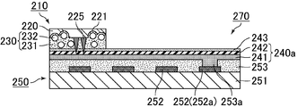
- 12A and 12B are schematic diagrams schematically showing how the ground member according to the third embodiment of the present invention is arranged on the shield printed wiring board.
- the shield printed wiring board 270 on which the ground member 210 is arranged covers the base film 251, the printed circuit 252 including the ground circuit 252 a arranged on the base film 251, and the printed circuit 252.
- the printed wiring board 250 includes a cover lay 253, a shield layer 240a formed on the cover lay 253, and a protective layer 243 formed on the shield layer 240a.
- An opening 253a exposing the ground circuit 252a is formed in the cover lay 253 of the printed wiring board 250.
- the shield layer 240a includes a conductive adhesive layer 241 and a metal thin film 242 laminated on the conductive adhesive layer 241.
- the shield layer 240a is arranged on the printed wiring board 250 so that the conductive adhesive layer 241 contacts the cover lay 253.
- the conductive adhesive layer 241 fills the opening 253a of the cover lay 253 and is in contact with the ground circuit 252a.
- the ground member 210 is arranged on the shield printed wiring board 270 so that the adhesive layer 230 contacts the protective layer 243.
- the conductive bumps 225 of the ground member 210 are pressed so as to penetrate the protective layer 243.
- the conductive bumps 225 come into contact with the metal thin film 242. That is, the conductive bumps 225 of the ground member 210 penetrate the protective layer 243 and are electrically connected to the conductive layer 220 and the shield layer 240a of the ground member 210.
- the hard particles 232 contained in the adhesive layer 230 of the ground member 210 form holes or depressions 221 in the conductive layer 220 through which volatile components can pass.
- the conductive layer 220 of the ground member 210 will be connected to an external ground (not shown). In this way, by using the ground member 210, the ground circuit 252a of the shield printed wiring board 270 and the external ground can be electrically connected.
- 13A, 13B, 13C, and 13D are schematic diagrams schematically showing how the ground member according to the third embodiment of the present invention is arranged on the shield printed wiring board.
- a printed wiring board 350 including a base film 351, a printed circuit 352 including a ground circuit 352 a arranged on the base film 351, and a cover lay 353 covering the printed circuit 352 is prepared. .. In the printed wiring board 350, a part of the ground circuit 352a is exposed by the opening 353a of the cover lay 353.
- the ground member 210 is arranged on the printed wiring board 350 such that the adhesive layer 230 is located on the opening 353a of the cover lay 353 of the printed wiring board 350.
- an electromagnetic wave shielding film 340 including a conductive adhesive layer 341 and a metal thin film 342 laminated on the conductive adhesive layer 341 is placed on the lower side of the conductive adhesive layer 341. Is arranged on the ground member 210 and the printed wiring board 350.
- the ground member 210 and the electromagnetic wave shield film 340 are pressure-bonded to the printed wiring board 350 by hot pressing to form a shield printed wiring board 370.
- the conductive bumps 225 of the ground member 210 penetrate the adhesive layer 230 and come into contact with the ground circuit 352a. Further, the hard particles 232 included in the adhesive layer 230 of the ground member 210 form holes or depressions 221 in the conductive layer 220 through which volatile components can pass.
- the electromagnetic wave shield film 340 becomes the shield layer 340a. Further, the conductive adhesive layer 341 of the shield layer 340a comes into contact with the conductive layer 220 of the ground member 210.
- the conductive layer 220 of the ground member 210 will be connected to an external ground (not shown). In this way, by using the ground member 210, the ground circuit 352a of the shield printed wiring board 370 and the external ground can be electrically connected.
- the base film 351, the printed circuit 352 (ground circuit 352a), the cover lay 353, the conductive adhesive layer 341, and the metal thin film 342 are the base film 51 in the shield printed wiring board 70.
Landscapes
- Engineering & Computer Science (AREA)
- Microelectronics & Electronic Packaging (AREA)
- Physics & Mathematics (AREA)
- Electromagnetism (AREA)
- Manufacturing & Machinery (AREA)
- Shielding Devices Or Components To Electric Or Magnetic Fields (AREA)
- Structure Of Printed Boards (AREA)
- Multi-Conductor Connections (AREA)
Abstract
Description
また、ノイズ対策の為、プリント配線板のグランド回路と、外部グランドとをシールド層を介して電気的に接続する方法も知られている。
また、特許文献1に記載のプリント配線板は、ベースフィルム上のプリントパターンが絶縁フィルム(カバーレイ)で被覆された構成となっている。
そのため、その後、さらに急激な加熱が行われると、グランド部材の導電層と接着剤層との間に溜まった揮発成分が膨張し、グランド部材の導電層-接着剤層間の層間密着が破壊されるという問題があった。
すなわち、シールドプリント配線板を製造する際、接着剤層がプリント配線板のカバーレイに接触するように、本発明のグランド部材はプリント配線板に配置されることになる。
その後、加熱プレスにより、グランド部材は、プリント配線板に接着・固定されることになる。
本発明のグランド部材の接着剤層に含まれる硬質粒子は、この加熱プレスにおいてグランド部材の導電層を押し、導電層に揮発成分が通過可能な孔や窪みを形成することになる。
そのため、シールドプリント配線板を製造する過程において、加熱により揮発成分が発生したとしても、揮発成分は導電層を通過することができる。
また、本発明のグランド部材が用いられたシールドプリント配線板に電子部品を搭載する場合、はんだリフロー工程においてシールドプリント配線板が加熱され揮発成分が発生したとしても、揮発成分は導電層を通過することができる。
すなわち、揮発成分がグランド部材の導電層-接着剤層間に溜まることを防止することができる
その結果、シールドプリント配線板の製造時や、シールドプリント配線板に電子部品を搭載する際の加熱により、グランド部材の導電層-接着剤層間の層間密着が破壊されることを防止することができる。
接着剤層の厚さが、5μm未満であると、接着力が不充分になる。
接着剤層の厚さが、30μmを超えると、加熱プレス時に硬質粒子が導電層を押す圧力が分散し、導電層に揮発成分が通過可能な孔や窪みを形成することができない。
硬質粒子のモース硬度が導電層のモース硬度の1.5倍以上であると、加熱プレス時に、硬質粒子は、導電層に埋まりやすくなる。
その結果、導電層に揮発成分が通過可能な孔や窪みを形成しやすくなる。
硬質粒子のモース硬度が4~7であると、加熱プレスの際に硬質粒子が潰れることなく導電層に揮発成分が通過可能な孔や窪みを形成しやすくなる。
硬質粒子の平均粒子径がこの範囲であると、加熱プレス時に、導電層に揮発成分が通過可能な孔や窪みを好適に形成することができる。
硬質粒子の平均粒子径が2.5μm未満であると、加熱プレス時に、導電層に充分な大きさの孔や窪みを形成しにくくなり、揮発成分が導電層を通過しにくくなる。
硬質粒子の平均粒子径が25μmを超えると、加熱プレス時に、導電層に形成される孔や窪みが大きくなり、導電層の強度が低下しやすくなる。
シリカは、モース硬度が充分に高く、硬質粒子として好適に機能する。
本発明のグランド部材が使用されたシールドプリント配線板では、グランド部材の導電層は、プリント配線板のグランド回路と電気的に接続されることになる。また、本発明のグランド部材が使用されたシールドプリント配線板では、導電層が外部グランドに接続されることになる。
グランド部材の導電層が、銅、銀、金及びニッケルからなる群から選択される少なくとも1種からなると、これらの材料は導電性に優れるので、グランド回路-外部グランド間の電気抵抗値を低くすることができる。
この場合、接着剤層が、導電性接着剤層として機能する。
硬質粒子の平均粒子径が、導電性粒子の平均粒子径よりも大きいと、硬質粒子がグランド部材の接着剤層から露出しやすくなる。そのため、接着剤層の密着性が失われやすくなる。
硬質粒子のモース硬度が、導電性粒子のモース硬度よりも高いと、本発明のグランド部材の被着体が柔らかかったとしても、導電層に揮発成分が通過可能な孔や窪みを形成しやすくなる。
本発明のグランド部材は、保護層と保護層に積層されたシールド層とを備える電磁波シールドフィルムに配置されることがある。
この際、電磁波シールドフィルムの保護層にグランド部材の接着剤層が接するように配置され、かつ、グランド部材の導電性粒子が電磁波シールドフィルムの保護層を貫通するように配置されることになる。
このような場合において、接着剤層におけるバインダー成分の厚さが、上記導電性粒子の平均粒子径よりも小さい場合、導電性粒子が電磁波シールドフィルムの保護層を確実に貫通し、導電性粒子と、電磁波シールドフィルムのシールド層とを接触させることができる。
本発明のグランド部材の導電層は、外部グランドに接続され、電磁波シールドフィルムのシールド層はプリント配線板のグランド回路に電気的に接続されることになる。
本発明のグランド部材の導電性粒子は、電磁波シールドフィルムの保護層を貫通し、電磁波シールドフィルムのシールド層と接触することになる。
このように、本発明のグランド部材を用いることにより、電磁波シールドフィルムが用いられたプリント配線板のグランド回路と外部グランドとを電気的に接続することができる。
本発明のグランド部材の導電層は、外部グランドに電気的に接続されることになる。
グランド部材の導電性粒子は、シールドプリント配線板の保護層を貫通してシールド層と接触することになる。
このように、本発明のグランド部材を用いることにより、シールドプリント配線板のグランド回路と外部グランドとを電気的に接続することができる。
グランド部材が導電性バンプを有すると、導電性バンプを介し、導電層と被着体とを電気的に接続することができる。
従ってシールドプリント配線板の製造時や、シールドプリント配線板に電子部品を搭載する際の加熱により、グランド部材の導電層-接着剤層間の層間密着が破壊されることを防止することができる。
シールドプリント配線板を製造する際の加熱プレスにおいて、本発明のグランド部材の接着剤層に含まれる硬質粒子は、グランド部材の導電層を押し、導電層に揮発成分が通過可能な孔や窪みを形成することになる。
そのため、シールドプリント配線板を製造する過程において、加熱により揮発成分が発生したとしても、揮発成分は導電層を通過することができる。すなわち、揮発成分がグランド部材の導電層-接着剤層間に溜まることを防止することができる
その結果、シールドプリント配線板の製造時や、シールドプリント配線板に電子部品を搭載する際の加熱により、グランド部材の導電層-接着剤層間の層間密着の破壊を防止することができる。
本発明の第1実施形態に係るグランド部材について、以下に図面を用いて説明する。
図1は、本発明の第1実施形態に係るグランド部材の一例を模式的に示す断面図である。
図1に示すように、グランド部材10は、導電層20と、導電層20に積層された接着剤層30とからなる。
また、接着剤層30は、バインダー成分31と硬質粒子32とを有する。
接着剤層30の厚さT30は、5~30μmである。
図2A、図2B及び図2Cは、従来のグランド部材を用いてプリント配線板を製造する場合の一例を模式的に示す模式図である。
この際、従来のグランド部材510の接着剤層530が、プリント配線板550側に配置されることになる。
そのため、その後、さらに急激な加熱が行われると、図2Cに示すように、従来のグランド部材510の導電層520と接着剤層530との間に溜まった揮発成分が膨張し、従来のグランド部材510の導電層520-接着剤層530間の層間密着が破壊されることがある。
図3A、図3B及び図3Cは、本発明の第1実施形態に係るグランド部材を用いてプリント配線板を製造する場合の一例を模式的に示す模式図である。
この際、グランド部材10の接着剤層30が、プリント配線板50側に配置されることになる。
図3Cに示すように、このような揮発成分60は孔や窪み21を通じ、導電層20を通過することができる。
すなわち、揮発成分60がグランド部材10の導電層20-接着剤層30間に溜まることを防止することができる
その結果、グランド部材10の導電層20-接着剤層30間の層間密着が破壊されることを防止することができる。
グランド部材10の導電層20の材料は特に限定されず、銅、銀、金及びニッケルからなる群から選択される少なくとも1種からなることが望ましい。
グランド部材10が使用されたシールドプリント配線板では、グランド部材10の導電層20は、プリント配線板のグランド回路と電気的に接続されることもある。また、グランド部材10が使用されたシールドプリント配線板では、導電層20が外部グランドに接続されることもある。
グランド部材10の導電層が、銅、銀、金及びニッケルからなる群から選択される少なくとも1種からなると、これらの材料は導電性に優れるので、グランド回路-外部グランド間の電気抵抗値を低くすることができる。
導電層の厚さが1μm未満であると、導電層の強度が低くなるので、破損しやすくなる。
導電層の厚さが9μmを超えると、導電層が厚すぎるので、硬質粒子により揮発成分が通過可能な孔や窪みが形成されにくくなる。
グランド部材10において、接着剤層30の厚さT30は、5~30μmである。
また、接着剤層30の厚さT30は、10~20μmであることが望ましい。
接着剤層の厚さが、5μm未満であると、接着力が不充分になる。
接着剤層の厚さが、30μmを超えると、加熱プレス時に硬質粒子が導電層を押す圧力が分散し、導電層に揮発成分が通過可能な孔や窪みを形成することができない。
硬質粒子32のモース硬度が導電層20のモース硬度の1.5倍以上であると、加熱プレス時に、硬質粒子32は、導電層20に埋まりやすくなる。
その結果、導電層20に揮発成分が通過可能な孔や窪み21を形成しやすくなる。
硬質粒子32のモース硬度が4~7であると、加熱プレスの際に硬質粒子32が潰れることなく導電層20に揮発成分が通過可能な孔や窪み21を形成しやすくなる。
硬質粒子32の平均粒子径がこの範囲であると、加熱プレス時に、導電層20に揮発成分が通過可能な孔や窪み21を好適に形成することができる。
硬質粒子の平均粒子径が2.5μm未満であると、加熱プレス時に、導電層に充分な大きさの孔や窪みを形成しにくくなり、揮発成分が導電層を通過しにくくなる。
硬質粒子の平均粒子径が25μmを超えると、加熱プレス時に、導電層に形成される孔や窪みが大きくなり、導電層の強度が低下しやすくなる。
シリカは、モース硬度が7であり充分に硬いので、硬質粒子として好適に機能する。
グランド部材10を用いたシールドプリント配線板の製造方法は、(1)プリント配線板準備工程と、(2)グランド部材配置工程と、(3)電磁波シールドフィルム配置工程と、(4)加熱プレス工程とを含む。
以下、各工程について図面を用いて説明する。
図4は、本発明の第1実施形態に係るグランド部材を用いたシールドプリント配線板の製造方法のプリント配線板準備工程の一例を模式的に示す模式図である。
図5は、本発明の第1実施形態に係るグランド部材を用いたシールドプリント配線板の製造方法のグランド部材配置工程の一例を模式的に示す模式図である。
図6は、本発明の第1実施形態に係るグランド部材を用いたシールドプリント配線板の製造方法の電磁波シールドフィルム配置工程の一例を模式的に示す模式図である。
図7A及び図7Bは、本発明の第1実施形態に係るグランド部材を用いたシールドプリント配線板の製造方法の加熱プレス工程の一例を模式的に示す模式図である。
本工程では、図4に示すように、ベースフィルム51、ベースフィルム51の上に配置されたグランド回路52aを含むプリント回路52、及び、プリント回路52を覆うカバーレイ53からなるプリント配線板50を準備する。
プリント配線板50では、グランド回路52aの一部は、カバーレイ53の開口部53aにより露出されている。
また、これらのエンジニアリングプラスチックの内、難燃性が要求される場合には、ポリフェニレンサルファイドフィルムが望ましく、耐熱性が要求される場合にはポリイミドフィルムが望ましい。
なお、ベースフィルム51の厚さは、10~40μmであることが望ましい。
また、カバーレイ53の厚さは、10~50μmであることが望ましい。
次に、図5に示すように、グランド部材10の接着剤層30がプリント配線板50のカバーレイ53に接するように、グランド部材10をプリント配線板50に配置する。
次に、図6に示すように、導電性接着剤層41と、導電性接着剤層41に積層された金属薄膜42からなる電磁波シールドフィルム40を準備する。
そして、電磁波シールドフィルム40の導電性接着剤層41がプリント配線板50のカバーレイ53及びグランド部材10の一部に接触するように電磁波シールドフィルム40をプリント配線板50に配置する。
この際、後述する加熱プレス工程後、電磁波シールドフィルム40の導電性接着剤層41が、プリント配線板50の開口部53aを埋め、電磁波シールドフィルム40の導電性接着剤層41と、グランド回路52aと接触するように電磁波シールドフィルム40を配置する。
また、後述する加熱プレス工程後、電磁波シールドフィルム40の導電性接着剤層41が、グランド部材10の導電層20と接触するように電磁波シールドフィルム40を配置する。
導電性粒子としては、特に限定されないが、銅粉、銀粉、ニッケル粉、銀コート銅粉、金コート銅粉、銀コートニッケル粉及び金コートニッケル粉からなる群から選択される少なくとも1種からなることが望ましい。
樹脂としては、スチレン系樹脂組成物、酢酸ビニル系樹脂組成物、ポリエステル系樹脂組成物、ポリエチレン系樹脂組成物、ポリプロピレン系樹脂組成物、イミド系樹脂組成物、アミド系樹脂組成物、アクリル系樹脂組成物、フェノール系樹脂組成物、エポキシ系樹脂組成物、ウレタン系樹脂組成物、メラミン系樹脂組成物、アルキッド系樹脂組成物等を使用することができる。
銅は、導電性及び経済性の観点から金属薄膜42にとって好適な材料である。
なお、金属薄膜42は、上記金属の合金からなる層を含んでいてもよい。
また、金属薄膜42としては金属箔を用いてもよく、スパッタリングや無電解めっき、電解めっき等の方法で形成された金属膜であってもよい。
次に、図7Aに示すように、プリント配線板50、グランド部材10及び電磁波シールドフィルム40を加熱プレスし、プリント配線板50にグランド部材10及び電磁波シールドフィルム40を圧着する。
この際、電磁波シールドフィルム40の導電性接着剤層41が、開口部53aを埋め、グランド回路52aと接触する。
また、電磁波シールドフィルム40の導電性接着剤層41が、グランド部材10の導電層20と接触する。
このような揮発成分は孔や窪み21を通じ、導電層20を通過することができる。
すなわち、揮発成分60がグランド部材10の導電層20-接着剤層30間に溜まることを防止することができる
その結果、グランド部材10の導電層20-接着剤層30間の層間密着が破壊されることを防止することができる。
加熱プレス工程におけるプレス圧力は、0.5~4.0Paであることが望ましく、2.0~3.0Paであることがより望ましい。
すなわち、図7Bに示すように、シールドプリント配線板70は、プリント配線板50と、シールド層40aと、グランド部材10からなる。
プリント配線板50は、ベースフィルム51、ベースフィルム51の上に配置されたグランド回路52aを含むプリント回路52、及び、プリント回路52を覆うカバーレイ53からなる。また、カバーレイ53には、グランド回路52aを露出する開口部53aが形成されている。
また、シールド層40aは、導電性接着剤層41がカバーレイ53と接触するようにプリント配線板50に配置されている。
そして、導電性接着剤層41は、カバーレイ53の開口部53aを埋め、グランド回路52aと接している。
グランド部材10は、接着剤層30がカバーレイ53に接触するようにプリント配線板50に配置されている。
そのため、グランド部材10の導電層20と、シールド層40aとは電気的に接続していることになる。
この場合、絶縁性接着剤層側の金属薄膜に複数の導電性バンプを形成し、又は、金属薄膜が突起形状をなすことにより、導電性バンプ又は突起形状の金属薄膜とプリント配線板のグランド回路とを接触させ、また、シールド層とグランド部材の導電層とを接触させ、さらにグランド部材の導電層と外部グランドとを接触させること等により、シールドプリント配線板のグランド回路と、外部グランドをと電気的に接続させてもよい。
本発明の第2実施形態に係るグランド部材について、以下に図面を用いて説明する。
図8は、本発明の第2実施形態に係るグランド部材の一例を模式的に示す断面図である。
図8に示すグランド部材110は、接着剤層130が、導電性粒子133を有する以外は、上記グランド部材10と同じ構成である。
また、接着剤層130は、バインダー成分131、硬質粒子132及び導電性粒子133をする。
接着剤層130の厚さT130は、5~30μmである。
硬質粒子132の平均粒子径が、導電性粒子133の平均粒子径よりも大きいと、硬質粒子132がグランド部材110の接着剤層130から露出しやすくなる。そのため、接着剤層130の密着性が失われやすくなる。
硬質粒子132のモース硬度が、導電性粒子133のモース硬度よりも高いと、グランド部材110の被着体が柔らかかったとしても、導電層120に揮発成分が通過可能な孔や窪みを形成しやすくなる。
図9A及び図9Bは、本発明の第2実施形態に係るグランド部材を、電磁波シールドフィルムに配置する様子を模式的に示す模式図である。
グランド部材110を電磁波シールドフィルム180に配置する場合、電磁波シールドフィルム180の保護層181にグランド部材110の接着剤層130が接触するように配置されることになる。
この際、グランド部材110の接着剤層130に含まれる硬質粒子132が、導電層120に、揮発成分が通過可能な孔や窪み121を形成する。
このように、グランド部材110を用いることにより、電磁波シールドフィルムが用いられたプリント配線板のグランド回路と外部グランドとを電気的に接続することができる。
接着剤層130におけるバインダー成分131の厚さが、導電性粒子133の平均粒子径よりも小さい場合、導電性粒子133が電磁波シールドフィルム180の保護層181を確実に貫通し、導電性粒子133と、電磁波シールドフィルム180のシールド層182とを接触させることができる。
このように、グランド部材110がシールドプリント配線板に配置される場合について図面を用いて説明する。
図10A及び図10Bは、本発明の第2実施形態に係るグランド部材を、シールドプリント配線板に配置する様子を模式的に示す模式図である。
プリント配線板150のカバーレイ153には、グランド回路152aを露出する開口部153aが形成されている。
また、シールド層140aは、導電性接着剤層141がカバーレイ153と接触するようにプリント配線板150に配置されている。
そして、導電性接着剤層141は、カバーレイ153の開口部153aを埋め、グランド回路152aと接している。
この際、グランド部材110の接着剤層130に含まれる硬質粒子132が、導電層120に、揮発成分が通過可能な孔や窪み121を形成する。
このように、グランド部材110を用いることにより、シールドプリント配線板170のグランド回路152aと外部グランドとを電気的に接続することができる。
接着剤層130におけるバインダー成分131の厚さが、導電性粒子133の平均粒子径よりも小さい場合、導電性粒子133が保護層143を確実に貫通し、導電性粒子133と、金属薄膜142とを接触させることができる。
シールドプリント配線板170における保護層143の望ましい材料は、エンジニアリングプラスチックからなることが望ましい。このようなエンジニアリングプラスチックとしては、例えば、ポリエチレンテレフタレート、ポリプロピレン、架橋ポリエチレン、ポリエステル、ポリベンズイミダゾール、ポリイミド、ポリイミドアミド、ポリエーテルイミド、ポリフェニレンサルファイドなどの樹脂が挙げられる。
また、これらのエンジニアリングプラスチックの内、難燃性が要求される場合には、ポリフェニレンサルファイドフィルムが望ましく、耐熱性が要求される場合にはポリイミドフィルムが望ましい。
本発明の第3実施形態に係るグランド部材について、以下に図面を用いて説明する。
図11は、本発明の第3実施形態に係るグランド部材の一例を模式的に示す断面図である。
図11に示すグランド部材210は、導電性バンプ225が形成されている以外は、上記グランド部材10と同じ構成である。
また、接着剤層230は、バインダー成分231と硬質粒子232とを有する。
接着剤層230の厚さT230は、5~30μmである。
また、接着剤層230は絶縁性を有する。
そして接着剤層230側の導電層220には、導電性バンプ225が形成されている。
導電性バンプの高さが10μm未満であると、導電性バンプが後述するシールドプリント配線板の保護層を貫きにくくなる。
導電性バンプの高さが40μmを超えると、導電性バンプを扱いにくくなる。
樹脂組成物の材料はこれらの1種単独であってもよく、2種以上の組み合わせであってもよい。
これらの中では、経済性の観点から、安価に入手できる銅粉又は銀コート銅粉であることが望ましい。
このように、グランド部材210がシールドプリント配線板に配置される場合について図面を用いて説明する。
図12A及び図12Bは、本発明の第3実施形態に係るグランド部材を、シールドプリント配線板に配置する様子を模式的に示す模式図である。
プリント配線板250のカバーレイ253には、グランド回路252aを露出する開口部253aが形成されている。
また、シールド層240aは、導電性接着剤層241がカバーレイ253と接触するようにプリント配線板250に配置されている。
そして、導電性接着剤層241は、カバーレイ253の開口部253aを埋め、グランド回路252aと接している。
この際、グランド部材210の接着剤層230に含まれる硬質粒子232が、導電層220に、揮発成分が通過可能な孔や窪み221を形成する。
このように、グランド部材210を用いることにより、シールドプリント配線板270のグランド回路252aと外部グランドとを電気的に接続することができる。
図13A、図13B、図13C及び図13Dは、本発明の第3実施形態に係るグランド部材を、シールドプリント配線板に配置する様子を模式的に示す模式図である。
プリント配線板350では、グランド回路352aの一部は、カバーレイ353の開口部353aにより露出されている。
また、グランド部材210の接着剤層230に含まれる硬質粒子232が、導電層220に、揮発成分が通過可能な孔や窪み221を形成する。
また、シールド層340aの導電性接着剤層341は、グランド部材210の導電層220と接触することになる。
このように、グランド部材210を用いることにより、シールドプリント配線板370のグランド回路352aと外部グランドとを電気的に接続することができる。
20、120、220、520 導電層
21、121、221 孔や窪み
30、130、230、530 接着剤層
31、131、231 バインダー成分
32、132、232 硬質粒子
40、180、340 電磁波シールドフィルム
40a、140a、182、240a、340a シールド層
41、141、241、341 導電性接着剤層
42、142、242、342 金属薄膜
50、150、250、350、550 プリント配線板
51、151、251、351、551 ベースフィルム
52、152、252、352、552 プリント回路
52a、152a、252a、352a グランド回路
53、153、253、353、553 カバーレイ
53a、153a、253a、353a 開口部
60、560 揮発成分
70、170、270、370 シールドプリント配線板
133 導電性粒子
143、181、243 保護層
255 導電性バンプ
Claims (17)
- 導電層と、前記導電層に積層された接着剤層とを含むグランド部材であって、
前記接着剤層は、バインダー成分と硬質粒子とを有し、
前記接着剤層の厚さは、5~30μmであることを特徴とするグランド部材。 - 前記硬質粒子のモース硬度は前記導電層のモース硬度の1.5倍以上である請求項1に記載のグランド部材。
- 前記硬質粒子のモース硬度は4~7である請求項1又は2に記載のグランド部材。
- 前記硬質粒子の平均粒子径は、2.5~25μmである請求項1~3のいずれかに記載のグランド部材。
- 前記硬質粒子は、シリカからなる請求項1~4のいずれかに記載のグランド部材。
- 前記導電層は、銅、銀、金及びニッケルからなる群から選択される少なくとも1種からなる請求項1~5のいずれかに記載のグランド部材。
- 前記接着剤層は、さらに導電性粒子を有する請求項1~6のいずれかに記載のグランド部材。
- 前記硬質粒子の平均粒子径は、前記導電性粒子の平均粒子径よりも小さい請求項7に記載のグランド部材。
- 前記硬質粒子のモース硬度は、前記導電性粒子のモース硬度よりも高い請求項7又は8に記載のグランド部材。
- 前記接着剤層におけるバインダー成分の厚さは、前記導電性粒子の平均粒子径よりも小さい請求項7~9のいずれかに記載のグランド部材。
- 前記グランド部材は、
保護層と前記保護層に積層されたシールド層とを備える電磁波シールドフィルムに対し、
前記保護層に前記接着剤層が接するように配置され、かつ、前記導電性粒子が前記保護層を貫通するように配置されることになる請求項7~10のいずれかに記載のグランド部材。 - 前記グランド部材は、
ベースフィルム、前記ベースフィルムの上に配置されたグランド回路を含むプリント回路、及び、前記プリント回路を覆うカバーレイからなるプリント配線板と、前記カバーレイの上に配置され、前記グランド回路と電気的に接続されたシールド層と、前記シールド層における前記プリント回路側と反対側の表面に設けられた保護層とを備えるシールドプリント配線板に配置されることになり、
前記グランド部材は、前記保護層に前記接着剤層が接するように配置され、かつ、前記導電性粒子が前記保護層を貫通するように配置されることになる請求項7~10のいずれかに記載のグランド部材。 - 前記接着剤層は絶縁性を有し、
前記接着剤層側の前記導電層には、導電性バンプが形成されている請求項1~6のいずれかに記載のグランド部材。 - ベースフィルム、前記ベースフィルムの上に配置されたグランド回路を含むプリント回路、及び、前記プリント回路を覆うカバーレイからなるプリント配線板と、
前記カバーレイの上に配置され、
前記グランド回路と電気的に接続されたシールド層とを備えるシールドプリント配線板であって、
前記シールドプリント配線板は、さらに請求項1~6のいずれかに記載のグランド部材を備え、
前記カバーレイに前記グランド部材の接着剤層が接するように、前記グランド部材が配置されており、
前記グランド部材の導電層と、前記シールド層とは電気的に接続していることを特徴とするシールドプリント配線板。 - ベースフィルム、前記ベースフィルムの上に配置されたグランド回路を含むプリント回路、及び、前記プリント回路を覆うカバーレイからなるプリント配線板と、
前記カバーレイの上に配置され、導電性接着剤層と、導電性接着剤層に積層されたシールド層からなり、前記導電性接着剤層と前記グランド回路と電気的に接続された電磁波シールドフィルムとを備えるシールドプリント配線板であって、
前記シールドプリント配線板は、さらに請求項1~6のいずれかに記載のグランド部材を備え、
前記カバーレイに前記グランド部材の接着剤層が接するように、前記グランド部材が配置されており、
前記グランド部材の導電層と、前記電磁波シールドフィルムの導電性接着剤層とは電気的に接続していることを特徴とするシールドプリント配線板。 - ベースフィルム、前記ベースフィルムの上に配置されたグランド回路を含むプリント回路、及び、前記プリント回路を覆うカバーレイからなるプリント配線板と、
前記カバーレイの上に配置され、前記グランド回路と電気的に接続されたシールド層と、
前記シールド層における前記プリント回路側と反対側の表面に設けられた保護層とを備えるシールドプリント配線板であって、
前記シールドプリント配線板は、さらに請求項7~10のいずれかに記載のグランド部材を備え、
前記保護層に前記グランド部材の接着剤層が接するように、前記グランド部材が配置されており、
前記グランド部材の導電性粒子は、前記保護層を貫通するとともに前記グランド部材の導電層及び前記シールド層と電気的に接続していることを特徴とするシールドプリント配線板。 - ベースフィルム、前記ベースフィルムの上に配置されたグランド回路を含むプリント回路、及び、前記プリント回路を覆うカバーレイからなるプリント配線板と、
前記カバーレイの上に配置され、前記グランド回路と電気的に接続されたシールド層と、
前記シールド層における前記プリント回路側と反対側の表面に設けられた保護層とを備えるシールドプリント配線板であって、
前記シールドプリント配線板は、さらに請求項13に記載のグランド部材を備え、
前記保護層に前記グランド部材の接着剤層が接するように、前記グランド部材が配置されており、
前記グランド部材の導電性バンプは、前記保護層を貫通するとともに前記グランド部材の導電層及び前記シールド層と電気的に接続していることを特徴とするシールドプリント配線板。
Priority Applications (4)
| Application Number | Priority Date | Filing Date | Title |
|---|---|---|---|
| US17/299,115 US11653439B2 (en) | 2018-12-03 | 2019-12-03 | Ground member and shielded printed wiring board |
| KR1020217016719A KR102640186B1 (ko) | 2018-12-03 | 2019-12-03 | 그라운드 부재 및 차폐 프린트 배선판 |
| JP2020559196A JP7282802B2 (ja) | 2018-12-03 | 2019-12-03 | グランド部材及びシールドプリント配線板 |
| CN201980079431.2A CN113170603B (zh) | 2018-12-03 | 2019-12-03 | 接地构件及屏蔽印制线路板 |
Applications Claiming Priority (2)
| Application Number | Priority Date | Filing Date | Title |
|---|---|---|---|
| JP2018-226550 | 2018-12-03 | ||
| JP2018226550 | 2018-12-03 |
Publications (1)
| Publication Number | Publication Date |
|---|---|
| WO2020116409A1 true WO2020116409A1 (ja) | 2020-06-11 |
Family
ID=70974274
Family Applications (1)
| Application Number | Title | Priority Date | Filing Date |
|---|---|---|---|
| PCT/JP2019/047104 Ceased WO2020116409A1 (ja) | 2018-12-03 | 2019-12-03 | グランド部材及びシールドプリント配線板 |
Country Status (6)
| Country | Link |
|---|---|
| US (1) | US11653439B2 (ja) |
| JP (1) | JP7282802B2 (ja) |
| KR (1) | KR102640186B1 (ja) |
| CN (1) | CN113170603B (ja) |
| TW (1) | TWI813823B (ja) |
| WO (1) | WO2020116409A1 (ja) |
Cited By (3)
| Publication number | Priority date | Publication date | Assignee | Title |
|---|---|---|---|---|
| WO2022097659A1 (ja) * | 2020-11-05 | 2022-05-12 | タツタ電線株式会社 | 電磁波シールドフィルム |
| WO2022131183A1 (ja) * | 2020-12-14 | 2022-06-23 | タツタ電線株式会社 | 電磁波シールドフィルム及びシールドプリント配線板 |
| US12349271B2 (en) | 2020-07-28 | 2025-07-01 | Samsung Electronics Co., Ltd. | Flexible printed circuit board assembly and electronic device including the same |
Families Citing this family (4)
| Publication number | Priority date | Publication date | Assignee | Title |
|---|---|---|---|---|
| TWI908940B (zh) * | 2021-03-31 | 2025-12-21 | 日商拓自達電線股份有限公司 | 電磁波屏蔽膜 |
| TWI908939B (zh) * | 2021-03-31 | 2025-12-21 | 日商拓自達電線股份有限公司 | 電磁波屏蔽膜 |
| EP4373224A4 (en) * | 2022-09-26 | 2025-03-12 | Samsung Electronics Co., Ltd. | FLEXIBLE CIRCUIT BOARD AND ELECTRONIC DEVICE THEREOF |
| CN120419300A (zh) * | 2023-01-20 | 2025-08-01 | 三星电子株式会社 | 包括用于屏蔽包括连接器的印刷电路板的结构的电子装置 |
Citations (5)
| Publication number | Priority date | Publication date | Assignee | Title |
|---|---|---|---|---|
| US20120048603A1 (en) * | 2010-08-30 | 2012-03-01 | Foxconn Advanced Technology Inc. | Printed circuit board and method for manufacturing same |
| WO2014132951A1 (ja) * | 2013-02-26 | 2014-09-04 | タツタ電線株式会社 | フレキシブルプリント配線板用補強部材、フレキシブルプリント配線板、及び、シールドプリント配線板 |
| JP2015053412A (ja) * | 2013-09-09 | 2015-03-19 | 東洋インキScホールディングス株式会社 | 電磁波シールドシートおよびプリント配線板 |
| JP2016122687A (ja) * | 2014-12-24 | 2016-07-07 | タツタ電線株式会社 | シールドプリント配線板 |
| JP2018039959A (ja) * | 2016-09-09 | 2018-03-15 | タツタ電線株式会社 | 導電性接着剤組成物 |
Family Cites Families (8)
| Publication number | Priority date | Publication date | Assignee | Title |
|---|---|---|---|---|
| JP2011066329A (ja) * | 2009-09-18 | 2011-03-31 | Tatsuta Electric Wire & Cable Co Ltd | シールドフィルム、そのシールドフィルムを有するシールド配線板、シールドフィルムにおけるグランド接続方法 |
| JP2012114217A (ja) * | 2010-11-24 | 2012-06-14 | Nitto Denko Corp | 配線回路基板の製造方法 |
| US9166141B2 (en) * | 2011-09-09 | 2015-10-20 | Dvx, Llc | Process of manufacturing a piezopolymer transducer with matching layer |
| JP2014123630A (ja) * | 2012-12-20 | 2014-07-03 | Tatsuta Electric Wire & Cable Co Ltd | シールドプリント配線板の製造方法、シールドフィルム、及び、シールドプリント配線板 |
| JP6715150B2 (ja) * | 2016-09-29 | 2020-07-01 | 信越ポリマー株式会社 | 電磁波シールドフィルム、電磁波シールドフィルムの製造方法および電磁波シールドフィルム付きプリント配線板の製造方法 |
| KR102267570B1 (ko) * | 2017-02-08 | 2021-06-18 | 타츠타 전선 주식회사 | 전자파 차폐 필름, 차폐 프린트 배선판 및 전자 기기 |
| CN109892020B (zh) * | 2017-02-13 | 2022-03-04 | 拓自达电线株式会社 | 接地构件、屏蔽印制线路板及屏蔽印制线路板的制造方法 |
| JP6898127B2 (ja) * | 2017-03-28 | 2021-07-07 | 信越ポリマー株式会社 | 電磁波シールドフィルムおよび電磁波シールドフィルム付きプリント配線板 |
-
2019
- 2019-12-03 JP JP2020559196A patent/JP7282802B2/ja active Active
- 2019-12-03 TW TW108144051A patent/TWI813823B/zh active
- 2019-12-03 KR KR1020217016719A patent/KR102640186B1/ko active Active
- 2019-12-03 CN CN201980079431.2A patent/CN113170603B/zh active Active
- 2019-12-03 US US17/299,115 patent/US11653439B2/en active Active
- 2019-12-03 WO PCT/JP2019/047104 patent/WO2020116409A1/ja not_active Ceased
Patent Citations (5)
| Publication number | Priority date | Publication date | Assignee | Title |
|---|---|---|---|---|
| US20120048603A1 (en) * | 2010-08-30 | 2012-03-01 | Foxconn Advanced Technology Inc. | Printed circuit board and method for manufacturing same |
| WO2014132951A1 (ja) * | 2013-02-26 | 2014-09-04 | タツタ電線株式会社 | フレキシブルプリント配線板用補強部材、フレキシブルプリント配線板、及び、シールドプリント配線板 |
| JP2015053412A (ja) * | 2013-09-09 | 2015-03-19 | 東洋インキScホールディングス株式会社 | 電磁波シールドシートおよびプリント配線板 |
| JP2016122687A (ja) * | 2014-12-24 | 2016-07-07 | タツタ電線株式会社 | シールドプリント配線板 |
| JP2018039959A (ja) * | 2016-09-09 | 2018-03-15 | タツタ電線株式会社 | 導電性接着剤組成物 |
Cited By (12)
| Publication number | Priority date | Publication date | Assignee | Title |
|---|---|---|---|---|
| US12349271B2 (en) | 2020-07-28 | 2025-07-01 | Samsung Electronics Co., Ltd. | Flexible printed circuit board assembly and electronic device including the same |
| WO2022097659A1 (ja) * | 2020-11-05 | 2022-05-12 | タツタ電線株式会社 | 電磁波シールドフィルム |
| JPWO2022097659A1 (ja) * | 2020-11-05 | 2022-05-12 | ||
| JP7180033B2 (ja) | 2020-11-05 | 2022-11-29 | タツタ電線株式会社 | 電磁波シールドフィルム |
| KR20230098792A (ko) * | 2020-11-05 | 2023-07-04 | 타츠타 전선 주식회사 | 전자파 차폐 필름 |
| TWI854159B (zh) * | 2020-11-05 | 2024-09-01 | 日商拓自達電線股份有限公司 | 電磁波屏蔽膜及屏蔽印刷配線板 |
| KR102862218B1 (ko) * | 2020-11-05 | 2025-09-18 | 타츠타 전선 주식회사 | 전자파 차폐 필름 |
| WO2022131183A1 (ja) * | 2020-12-14 | 2022-06-23 | タツタ電線株式会社 | 電磁波シールドフィルム及びシールドプリント配線板 |
| JPWO2022131183A1 (ja) * | 2020-12-14 | 2022-06-23 | ||
| CN116472171A (zh) * | 2020-12-14 | 2023-07-21 | 拓自达电线株式会社 | 电磁波屏蔽薄膜和屏蔽印刷电路板 |
| JP7620644B2 (ja) | 2020-12-14 | 2025-01-23 | タツタ電線株式会社 | 電磁波シールドフィルム及びシールドプリント配線板 |
| TWI901746B (zh) * | 2020-12-14 | 2025-10-21 | 日商拓自達電線股份有限公司 | 電磁波屏蔽膜及屏蔽印刷配線板 |
Also Published As
| Publication number | Publication date |
|---|---|
| CN113170603B (zh) | 2025-03-28 |
| JP7282802B2 (ja) | 2023-05-29 |
| JPWO2020116409A1 (ja) | 2021-10-14 |
| TW202106153A (zh) | 2021-02-01 |
| KR102640186B1 (ko) | 2024-02-22 |
| US20220061150A1 (en) | 2022-02-24 |
| CN113170603A (zh) | 2021-07-23 |
| KR20210095876A (ko) | 2021-08-03 |
| TWI813823B (zh) | 2023-09-01 |
| US11653439B2 (en) | 2023-05-16 |
Similar Documents
| Publication | Publication Date | Title |
|---|---|---|
| JP7282802B2 (ja) | グランド部材及びシールドプリント配線板 | |
| JP6959948B2 (ja) | シールドフィルム、シールドプリント配線板及びシールドプリント配線板の製造方法 | |
| JP6891218B2 (ja) | グランド部材、シールドプリント配線板及びシールドプリント配線板の製造方法 | |
| TWI501708B (zh) | Shielded printed circuit boards | |
| JP7256618B2 (ja) | 転写フィルム付電磁波シールドフィルム、転写フィルム付電磁波シールドフィルムの製造方法及びシールドプリント配線板の製造方法 | |
| JP7244534B2 (ja) | 電磁波シールドフィルム、シールドプリント配線板の製造方法、及び、シールドプリント配線板 | |
| JP6349250B2 (ja) | シールドプリント配線板 | |
| JP7244535B2 (ja) | 電磁波シールドフィルム、シールドプリント配線板の製造方法、及び、シールドプリント配線板 | |
| US12028964B2 (en) | Shielded printed wiring board, method for manufacturing shielded printed wiring board, and connecting member | |
| WO2018147424A1 (ja) | プリント配線板 | |
| WO2020122071A1 (ja) | シールドプリント配線板の製造方法及びシールドプリント配線板 | |
| KR102640159B1 (ko) | 차폐 프린트 배선판 및 차폐 프린트 배선판의 제조 방법 | |
| KR20190109302A (ko) | 전자파 차폐 필름 및 차폐 프린트 배선판 | |
| HK40050176A (en) | Ground member and shielded printed wiring board | |
| HK40050176B (zh) | 接地构件及屏蔽印制线路板 | |
| US12101872B2 (en) | Shield printed wiring board with ground member and ground member | |
| WO2019031555A1 (ja) | 接続用フィルム、シールドプリント配線板の製造方法、及び、シールドプリント配線板 | |
| HK40104319A (zh) | 电磁波屏蔽膜和屏蔽印刷线路板 | |
| TW202316949A (zh) | 電磁波屏蔽膜及屏蔽印刷配線板 |
Legal Events
| Date | Code | Title | Description |
|---|---|---|---|
| 121 | Ep: the epo has been informed by wipo that ep was designated in this application |
Ref document number: 19893478 Country of ref document: EP Kind code of ref document: A1 |
|
| ENP | Entry into the national phase |
Ref document number: 2020559196 Country of ref document: JP Kind code of ref document: A |
|
| NENP | Non-entry into the national phase |
Ref country code: DE |
|
| 122 | Ep: pct application non-entry in european phase |
Ref document number: 19893478 Country of ref document: EP Kind code of ref document: A1 |
|
| WWG | Wipo information: grant in national office |
Ref document number: 201980079431.2 Country of ref document: CN |