WO2020116207A1 - Microled mounting structure, microled display, and microled display manufacturing method - Google Patents
Microled mounting structure, microled display, and microled display manufacturing method Download PDFInfo
- Publication number
- WO2020116207A1 WO2020116207A1 PCT/JP2019/045816 JP2019045816W WO2020116207A1 WO 2020116207 A1 WO2020116207 A1 WO 2020116207A1 JP 2019045816 W JP2019045816 W JP 2019045816W WO 2020116207 A1 WO2020116207 A1 WO 2020116207A1
- Authority
- WO
- WIPO (PCT)
- Prior art keywords
- adhesive
- micro led
- led
- electrode
- wiring board
- Prior art date
Links
Images


Classifications
-
- G—PHYSICS
- G09—EDUCATION; CRYPTOGRAPHY; DISPLAY; ADVERTISING; SEALS
- G09F—DISPLAYING; ADVERTISING; SIGNS; LABELS OR NAME-PLATES; SEALS
- G09F9/00—Indicating arrangements for variable information in which the information is built-up on a support by selection or combination of individual elements
- G09F9/30—Indicating arrangements for variable information in which the information is built-up on a support by selection or combination of individual elements in which the desired character or characters are formed by combining individual elements
- G09F9/33—Indicating arrangements for variable information in which the information is built-up on a support by selection or combination of individual elements in which the desired character or characters are formed by combining individual elements being semiconductor devices, e.g. diodes
-
- H—ELECTRICITY
- H01—ELECTRIC ELEMENTS
- H01L—SEMICONDUCTOR DEVICES NOT COVERED BY CLASS H10
- H01L33/00—Semiconductor devices with at least one potential-jump barrier or surface barrier specially adapted for light emission; Processes or apparatus specially adapted for the manufacture or treatment thereof or of parts thereof; Details thereof
- H01L33/36—Semiconductor devices with at least one potential-jump barrier or surface barrier specially adapted for light emission; Processes or apparatus specially adapted for the manufacture or treatment thereof or of parts thereof; Details thereof characterised by the electrodes
-
- H—ELECTRICITY
- H01—ELECTRIC ELEMENTS
- H01L—SEMICONDUCTOR DEVICES NOT COVERED BY CLASS H10
- H01L33/00—Semiconductor devices with at least one potential-jump barrier or surface barrier specially adapted for light emission; Processes or apparatus specially adapted for the manufacture or treatment thereof or of parts thereof; Details thereof
- H01L33/48—Semiconductor devices with at least one potential-jump barrier or surface barrier specially adapted for light emission; Processes or apparatus specially adapted for the manufacture or treatment thereof or of parts thereof; Details thereof characterised by the semiconductor body packages
- H01L33/50—Wavelength conversion elements
-
- H—ELECTRICITY
- H01—ELECTRIC ELEMENTS
- H01L—SEMICONDUCTOR DEVICES NOT COVERED BY CLASS H10
- H01L33/00—Semiconductor devices with at least one potential-jump barrier or surface barrier specially adapted for light emission; Processes or apparatus specially adapted for the manufacture or treatment thereof or of parts thereof; Details thereof
- H01L33/48—Semiconductor devices with at least one potential-jump barrier or surface barrier specially adapted for light emission; Processes or apparatus specially adapted for the manufacture or treatment thereof or of parts thereof; Details thereof characterised by the semiconductor body packages
- H01L33/62—Arrangements for conducting electric current to or from the semiconductor body, e.g. lead-frames, wire-bonds or solder balls
Definitions
- the present invention relates to a micro LED mounting structure in which a micro LED (light emitting diode) is mounted on a wiring board, and in particular, the bonding and conduction between the electrodes of the micro LED and the electrode portion of the wiring board can be reliably performed, and the micro LED and wiring
- the present invention relates to a micro LED mounting structure that can be reliably connected to a substrate, a micro LED display using the micro LED mounting structure, and a method for manufacturing the micro LED display.
- the adhesive layer has an insulating property, when the electrode wiring of the wiring board and the electrode of the micro LED are brought into contact with each other to be adhered, the adhesive layer separates the electrode wiring from the electrode of the micro LED. When an event such as seeping into the boundary surface occurs, there is a risk that conduction will not be achieved.
- the present invention addresses such a problem, and can reliably bond and electrically connect the electrode of the micro LED and the electrode portion of the wiring board, and securely connect the micro LED and the wiring board. It is an object of the present invention to provide a micro LED mounting structure, a micro LED display adopting the micro LED mounting structure, and a method for manufacturing the micro LED display.
- a micro LED mounting structure is provided with a wiring board having an electrode portion arranged on one side according to a predetermined arrangement and a position corresponding to the position of the electrode portion. To a blue wavelength band, it emits light having a specific spectrum, has an electrode that is conductively connected to the electrode portion on one of the opposite surfaces, and has a light emitting surface on the other surface.
- An LED is provided, and the electrode of the micro LED and the electrode portion of the wiring board are bonded to each other via a thermosetting first adhesive having conductivity. All or part of the micro LED is surrounded and adhered by an insulating thermosetting second adhesive, and the micro LED is fixed to the wiring board via the second adhesive. is there.
- a micro LED display according to the present invention is a micro LED display capable of full color display, in which a wiring board having an electrode portion arranged according to a predetermined arrangement on one surface is provided with the electrode. Depending on the position of the part, it emits light having a specific spectrum in the ultraviolet to blue wavelength band, and has an electrode that is conductively connected to the electrode part of the wiring board on one of the opposite surfaces.
- an LED array substrate having a micro LED having a light emitting surface on the other surface is mounted on the LED array substrate, and the three primary colors of light R( A fluorescent light emitting layer array having a plurality of fluorescent light emitting layers each containing a fluorescent material that converts wavelengths into fluorescent light of corresponding colors of red), G (green), and B (blue), and the electrodes of the micro LED and the wiring board.
- a fluorescent light emitting layer array having a plurality of fluorescent light emitting layers each containing a fluorescent material that converts wavelengths into fluorescent light of corresponding colors of red), G (green), and B (blue) the electrodes of the micro LED and the wiring board.
- the micro LED is adhered via a first thermosetting adhesive having conductivity, and a part or all of the peripheral side surface of the micro LED has a second thermosetting type having an insulating property.
- the micro LED is surrounded and adhered to the wiring board, and is fixed to the wiring board via the second adhesive.
- a method for manufacturing a micro LED display according to the present invention is a method for manufacturing a micro LED display capable of full color display, wherein a light having a specific spectrum from ultraviolet to blue wavelength band is emitted.
- a transparent substrate on the surface of which a micro-LED that emits light and has an electrode on one surface of the opposite surface and a light emitting surface on the other surface is formed according to a predetermined arrangement.
- the electrode of the micro LED and the electrode portion of the wiring board are bonded via the first adhesive having conductivity.
- the electrodes of the micro LEDs and the electrode portions of the wiring board can be reliably bonded and conducted.
- the second adhesive having an insulating property surrounds a part or all of the peripheral side surface of the micro LED including the electrode in which the first adhesive is laminated. Since they are adhered, the micro LED can be reliably fixed and connected to the wiring board via the second adhesive.
- the micro LED mounting structure of the present invention since the micro LED mounting structure of the present invention is included, the electrode of the micro LED and the electrode portion of the wiring board can be reliably bonded and conducted, and The micro LED can be securely fixed and connected to the wiring board via the second adhesive.
- micro LED display of the present invention it is possible to manufacture a micro LED display including the micro LED mounting structure of the present invention.
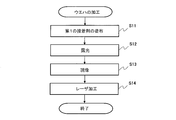
- FIG. 1 is a plan view schematically showing an embodiment of a micro LED display according to the present invention. It is explanatory drawing which shows the micro LED mounting structure by this invention. It is explanatory drawing which shows an example of a cell. It is a detailed explanatory view of the cell shown in FIG. 3 is a flowchart showing steps of a method for manufacturing a micro LED display according to the present invention. It is explanatory drawing which shows an example of a wafer. It is a flowchart which shows the process of processing a wafer. It is explanatory drawing which shows the state by which the 1st adhesive agent was laminated
- FIG. 6 is a process diagram illustrating a process from alignment to bonding shown in FIG. 5.
- FIG. 6 is a process diagram illustrating a process from pressing to separation of a wafer shown in FIG. 5. It is a graph which shows the temperature characteristic of the viscosity of a 1st adhesive agent and a 2nd adhesive agent.
- FIG. 1 is a plan view schematically showing an embodiment of a micro LED display according to the present invention.
- This micro LED display is a device capable of full color display by combining a micro LED and an RGB phosphor, and includes an LED array substrate 1 and a fluorescent light emitting layer array 2.
- the micro LED display according to the present invention can be applied to a flat display or a flexible display. When this micro LED display is applied to, for example, a flat display, illustration of a protective glass as another component is omitted in FIG. 1.
- the LED array substrate 1 is for individually emitting micro LEDs 3 (hereinafter, simply referred to as “LED3”), and includes a plurality of LEDs 3 arranged in a matrix as shown in FIG. 1 and a wiring substrate for driving the LEDs 3. Including 4 and.
- the fluorescent light emitting layer array 2 is excited by the light (excitation light) emitted from the LED 3 and wavelength-converted into fluorescence of corresponding colors of R (red), G (green) and B (blue) which are the three primary colors of light. And a plurality of fluorescent light emitting layers containing the fluorescent material.
- the fluorescent light emitting layer array 2 has a plurality of fluorescent light emitting layers 11 arranged in a matrix.
- a combination of three LEDs 3 corresponding to one pixel and one fluorescent light emitting layer 11 including the fluorescent material layers 11R, 11G, and 11B provided on each LED 3 is one cell. 21. That is, by combining the LED array substrate 1 and the fluorescent light emitting layer array 2, the cells 21 can be handled as a unit. As a result, in the micro LED display, the plurality of cells 21 for realizing full-color display are arranged in a matrix. In FIG. 1, the cells 21 are arranged in 4 rows and 5 columns for easy understanding of the description.
- the fluorescent light emitting layer 11 has a fluorescent material layer 11R filled with a red fluorescent dye, a fluorescent material layer 11G filled with a green fluorescent dye, and a fluorescent material layer 11B filled with a blue fluorescent dye. These fluorescent dyes are examples of RGB phosphors.
- the LED 3 emits light having a specific spectrum and is manufactured using gallium nitride (GaN) as a main material.
- the LED 3 is an ultraviolet light emitting diode (UV-LED), and is an LED that emits near-ultraviolet light having a wavelength of, for example, 200 nm to 380 nm.
- the LED 3 may be an LED that emits blue light having a wavelength of, for example, 380 nm to 500 nm.
- Near-ultraviolet light having a wavelength of, for example, 200 nm to 380 nm and blue light having a wavelength of, for example, 380 nm to 500 nm correspond to an example of light having a specific spectrum.
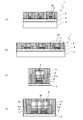
- FIG. 2 is an explanatory view showing a micro LED mounting structure according to the present invention.
- the LED array substrate 1 is an example of a micro LED mounting structure according to the present invention.
- FIG. 2A shows a sectional view taken along the line AA of the LED array substrate 1 in the region surrounded by the broken line R1 shown in FIG. 2B is a sectional view taken along line BB of the LED array substrate 1 in the area surrounded by the broken line R1 shown in FIG. 2C is an enlarged view of a main part of the LED array substrate 1 surrounded by a broken line R2 shown in FIG. 2A, and FIG. 2D is a broken line R3 shown in FIG. 2B. It is a principal part enlarged view of the LED array substrate 1 enclosed.
- the LED array substrate 1 has a wiring substrate 4 on a base substrate 5, the LEDs 3 are connected on the wiring substrate 4, and a flattening film 9 is further laminated. It has a structure. Then, the wiring board 4 and the LED 3 are excellently realized by a first adhesive 6 and a second adhesive 8, which will be described later, in a mechanical connection and an electrical connection.
- the LED 3 has a compound semiconductor 30 including a plurality of layers such as a peeling layer for laser lift-off and a light emitting layer.
- the LED 3 has LED electrodes 31a and 31b for light emission at a predetermined position on one surface of the compound semiconductor 30, and a light emitting surface 32 for emitting light from a light source (light emitting layer) on the other surface. Are formed.
- Laser lift-off is, for example, a means of irradiating an LED formed on one surface of a sapphire substrate with laser light by pulse oscillation from the other surface of the sapphire substrate to separate each LED from the sapphire substrate.
- a laser beam by focusing and irradiating a laser beam on an interface region (for example, a peeling layer) at a portion to be peeled off, for example, due to a phenomenon that nitrogen of GaN is vaporized, an LED is emitted in the interface region. It is separated from the sapphire substrate.
- a YAG laser oscillator in the solid-state UV (Ultra Violet) region uses a fourth harmonic (FHG: Fourth-Harmonic Generation) wavelength of 266 nm. It is preferable to use a picosecond pulsed laser.
- the wafer 10 which is a transparent substrate such as sapphire is adjusted by adjusting parameters such as laser power, a laser beam irradiation region, and the number of times of irradiation based on pulse irradiation using a device for performing laser lift-off. (See FIG. 6) is not peeled from the LED 3, but the wafer 10 is easily peeled from the LED 3. Details will be described later with reference to FIGS. 9 to 11.
- the wiring board 4 is, for example, a flexible printed wiring board (FPC: Flexible Printed Circuits), and is a film-like board including an insulating base film (for example, polyimide) and a wiring layer on which an electric circuit is formed. is there.
- the wiring board 4 has bump electrodes 7 for conductive connection arranged on one surface in accordance with a predetermined arrangement. Wiring is provided on the wiring board 4 so that a driving circuit (not shown) provided outside can supply a driving current for turning on and off to each of the plurality of LEDs 3.
- the base substrate 5 supports the wiring substrate 4 on which the LEDs 3 are mounted, and is a transparent substrate such as quartz glass.
- the first adhesive 6 ensures adhesion and conduction between the LED electrodes 31a and 31b and the bump electrodes 7.
- the first adhesive 6 is a resin composition that is laminated on the LED electrode surface of each LED 3 and includes a thermosetting adhesive having conductivity and the like.
- the bump electrode 7 is an example of an electrode portion, is provided on the wiring board 4, and is electrically connected to the LED electrodes 31a and 31b (see FIG. 2D) of the LED 3 via the first adhesive 6. It is a possible electrode.
- the bump electrode 7 has, for example, conductivity and is elastically deformed by applying pressure. As a result, the connection between the LED electrodes 31a and 31b of the LED 3 and the wiring board 4 becomes more reliable.
- the second adhesive 8 is provided on the wiring board 4 and is adhered so as to surround part or all of the peripheral side surface of the LED 3 including the LED electrodes 31a and 31b in which the first adhesive 6 is laminated.
- the flattening film 9 is a film that is laminated in a region including the light emitting surface 32 of the LED 3 and has a flat plate shape.
- the thickness of the flattening film 9 is determined on the light emitting surface 32 based on the emission angle of the light emitted from the light emitting surface 32. Details will be described later with reference to FIGS.
- each LED 3 is pressed against the bump electrode 7 via the first adhesive 6, and the first bonding is performed.
- the agent 6 and the second adhesive 8 are cured by heating.
- the LED electrodes 31a and 31b of the LED 3 and the bump electrodes 7 of the wiring board 4 are bonded together via the first adhesive 6. Specifically, as described later, the LED electrode 31a and the bump electrode 7 (anode electrode 7a shown in FIG. 13) are adhered to each other via the first adhesive 6. Further, the LED electrode 31b and the bump electrode 7 (cathode electrode 7b shown in FIG. 13) are adhered to each other via the first adhesive 6. Further, a part of the peripheral side surface of the LED 3 is surrounded and adhered by the second adhesive agent 8, and each LED 3 is fixed to the wiring board 4 via the second adhesive agent 8. The entire peripheral side surface of the LED 3 may be surrounded and adhered by the second adhesive 8.
- FIG. 3 is an explanatory diagram showing an example of a cell.
- FIG. 4 is a detailed explanatory diagram of the cell shown in FIG. 3A is a plan view of the cell 21 shown in FIG. 1, and FIG. 3B is a sectional view taken along the line CC shown in FIG. 3A.
- the cell 21 does not include the wiring substrate 4 and the base substrate 5.
- the fluorescent light emitting layer 11 uses red light (R) for realizing full-color display of red, green, and blue fluorescent dyes (an example of a fluorescent material) by light (excitation light) emitted from the light emitting surface 32 of the LED 3. The wavelengths are converted into green (G) and blue (B) fluorescence, respectively.
- the fluorescent light emitting layer 11 causes the fluorescent dyes of the respective fluorescent material layers 11R, 11G, and 11B to transition to an excited state by excitation light, and then, when the fluorescent dyes return to the ground state, the respective fluorescent materials convert wavelengths.
- the emitted red (R), green (G), and blue (B) corresponding to the visible spectrum emits fluorescence.
- These fluorescent material layers 11R, 11G, and 11B are partitioned by partition walls 12 having a reflective film 13 on the surface.
- the fluorescent light emitting layer 11 is provided on the LED array substrate 1.
- the fluorescent material layer 11R of the fluorescent light emitting layer 11 is formed by mixing and dispersing a fluorescent dye 14a having a particle size of micron size and a fluorescent dye 14b having a particle size of nanosize in a resist film.
- the fluorescent material layer 11G is formed by mixing and dispersing a fluorescent dye 14c having a micron-sized particle diameter and a fluorescent pigment 14d having a nano-sized particle diameter, like the fluorescent material layer 11R.
- the fluorescent material layer 11B is formed by mixing and dispersing a fluorescent dye 14e having a particle size of micron size and a fluorescent dye 14f having a particle size of nano size.
- a fluorescent dye 14e having a particle size of micron size and a fluorescent dye 14f having a particle size of nano size.
- the fluorescent dyes with nano-sized particles can prevent the leakage of excitation light due to the decrease in the packing ratio of the fluorescent dyes, and the fluorescent dyes with micron-sized particles can be used. Can improve the luminous efficiency.
- the partition wall 12 is an example of a light shielding wall, and separates the fluorescent material layers 11R, 11G, and 11B from each other.
- the partition wall 12 is formed of, for example, a transparent photosensitive resin.
- the partition wall 12 in order to increase the filling rate of the fluorescent dye 14a having a particle size larger than that of the fluorescent dye 14b, the partition wall 12 has an aspect ratio of height to width of 3 or more. It is desirable to use high aspect materials that allow. The same applies to the fluorescent material layers 11G and 11B.
- An example of such a high aspect material is SU-83000 photoresist manufactured by Nippon Kayaku Co., Ltd.
- a reflective film 13 is provided on the surface of the partition wall 12, as shown in FIG.
- the reflective film 13 prevents the excitation light and the fluorescent light FL from passing through the partition wall 12 and entering into another adjacent fluorescent material layer.
- This fluorescent light FL emits light when each fluorescent dye of each fluorescent material layer 11R, 11G, and 11B is excited by excitation light.
- the reflective film 13 is formed with a thickness that can sufficiently block the excitation light and the fluorescent light FL.
- the reflection film 13 is preferably a thin film of aluminum or aluminum alloy that easily reflects the excitation light and the fluorescent light FL.
- the fluorescent light emitting layer 11 can be used to emit light from the fluorescent material layers 11R, 11G, and 11B by reflecting the excitation light toward the partition wall 12 with the reflective film 13 such as aluminum. Therefore, the luminous efficiency of each of the fluorescent material layers 11R, 11G, and 11B is improved.
- the thin film deposited on the surface of the partition wall 12 is not limited to the reflective film 13 that reflects the excitation light and the fluorescence FL, and may be one that absorbs the excitation light and the fluorescence FL.
- the configuration of the micro LED display of the present invention has been described above.
- the LED electrodes 31a and 31b of each LED 3 and the bump electrode 7 are connected via the first adhesive 6 having conductivity, and the bumps 7 are attached to the peripheral side surface of the LED 3.
- a part of the LED 3 is surrounded and adhered by a second adhesive having an insulating property, and the LED 3 is fixed to the wiring board 4 via the second adhesive.
- the LED electrodes 31a and 31b of the LED 3 and the bump electrodes 7 of the wiring board 4 can be reliably bonded and conducted, and the LED 3 is bonded via the second adhesive.
- the wiring board 4 can be securely fixed and connected. That is, in the micro LED mounting structure according to the present invention, the electrical and mechanical connection between the LED 3 and the wiring board 4 can be reliably performed.
- the micro LED display of the present invention since the LED array substrate 1 is provided as the micro LED mounting structure, it is possible to surely perform the electrical and mechanical connection between the LED 3 and the wiring substrate 4. Then, by supplying a drive current to the wiring board 4 from a drive circuit provided outside, the micro LED display of the present invention can perform full color display.
- FIG. 5 is a flowchart showing steps of the method for manufacturing a micro LED display according to the present invention.
- FIG. 6 is an explanatory diagram showing an example of a wafer.
- FIG. 3A is a plan view of the wafer 10.
- (B) is a DD line sectional view of (a)
- (c) is a EE line sectional view of (a).
- a wafer 10 having a plurality of LEDs 3 arranged in a matrix (3 rows and 6 columns) at a predetermined interval on one surface (front surface) is used to A method for manufacturing the LED display will be described.
- the plurality of LEDs 3 are formed on one surface of the wafer 10 by a crystal growth process such as MOCVD (Metal Organic Chemical Vapor Deposition).
- MOCVD Metal Organic Chemical Vapor Deposition
- the LEDs 3 are arranged, for example, with a pitch of W 1 in the column direction (y direction) and with a pitch of W 2 in the row direction (x direction). ..
- the ratio P 1 (W 2 /W 1 ) between W 1 and W 2 is preferably about 3 in the arrangement shown in FIG. Therefore, for example, the pitch of W 1 is 50 ⁇ m and the pitch of W 2 is 150 ⁇ m.
- the height (h 1 ) for example, a size of several ⁇ m to 30 ⁇ m can be targeted.
- FIG. 7 is a flowchart showing the steps of wafer processing.
- the processes from step S11 to step S14 shown in FIG. 7 are performed.
- a photolithography technique using a photomask (not shown) is applied to apply the thermosetting first adhesive 6 having conductivity and photosensitivity to the wafer 10. Apply.
- the first adhesive 6 is laminated on the LED electrodes 31a and 31b by patterning by exposure and development. The details will be described below.
- the first adhesive 6 is applied on the surface of the wafer 10 on which the LEDs 3 are arranged.
- the first adhesive 6 is, for example, a resin composition in which an electrically conductive material, an adhesive material, and a photosensitizer are mixed with an insulating thermosetting resin.
- the first adhesive 6 is a resin composition that develops an adhesive function and is cured by heating.
- the adhesive material may be, for example, a thermosetting epoxy resin.
- the first adhesive 6 contains, as a conductive material, for example, fine carbon particles selected from a particle diameter in the range of 10 nm to 1.0 ⁇ m, and has a conductive function added. .. In the present embodiment, as an example, fine particles of carbon of about 0.5 ⁇ m to 1.0 ⁇ m are used.
- the first adhesive 6 contains a photosensitizer, it has a photosensitivity function capable of patterning by ultraviolet rays. That is, the first adhesive 6 also functions as a photoresist.
- the first adhesive 6 may be a resin composition in which a conductive material and a photosensitizer are mixed, and the adhesive strength is further increased. Adhesive materials may be included to enhance.
- the conductive material is not limited to the above-mentioned carbon, and metal fine particles may be adopted.
- the fine metal particles are preferably silver (Ag), for example.
- nickel (Ni), copper (Cu), aluminum (Al), gold (Au) or the like may be adopted depending on the application.
- an applicable material may be selected from metal nanoparticles having a metal particle diameter of about 10 nm to metal fine particles having a particle diameter of 1.0 ⁇ m or less.
- step S11 the first adhesive 6 is applied onto the surface of the wafer 10 on which the LEDs 3 are arranged, for example, using a spin coater (not shown) used in photolithography technology.
- the spin coater is a device for realizing uniform coating.
- the first adhesive 6 is dropped onto the wafer 10 as a photoresist, and the wafer 10 is set on the surface of the wafer 10 by setting a predetermined rotation speed and rotation time.
- Adhesive 6 of No. 1 is applied.
- a bar coater may be applied as a means for applying a uniform film thickness.
- the wafer 10 coated with the first adhesive 6 is pre-baked by a heating means such as a heater (not shown).
- the prebaking conditions are, for example, a heating temperature of 100° C. and a heating time of 1 minute.
- step S12 the wafer 10 coated with the first adhesive 6 is irradiated with ultraviolet (UV) light through a photomask.
- step S13 the wafer 10 is immersed in a developing solution for cleaning. As a result, the first adhesive 6 is laminated on the LED electrodes 31a and 31b.
- FIG. 8 is an explanatory diagram showing a state in which the first adhesive is laminated on the LED electrodes.
- FIG. 3A is a plan view of the surface of the wafer 10.
- (B) is the FF line sectional view of (a)
- (c) is the GG line sectional view of (a).
- the film thickness (h 2 ) of the first adhesive 6 laminated on the LED electrodes 31a and 31b is, for example, 2 ⁇ m.
- the interface between the wafer 10 and the LED 3 is focused and irradiated with the laser light L from the back surface of the wafer 10.
- the laser beam L is irradiated from the back surface of the wafer 10 to weaken the bonding state of the LEDs 3 formed on the front surface of the wafer 10 as compared with that before the laser beam L is irradiated.
- Perform processing In this case, in step S14, the laser lift-off for peeling the LED 3 from the wafer 10 is not performed, but the LED 3 is easily peeled off.
- the state of easy peeling means a state in which the adhesive force of the second adhesive 8 bonded to the LED 3 is larger than the adhesive force of the LED 3 bonded to the wafer 10 in the bonded state.
- FIG. 9 to 11 are explanatory views of laser processing.
- (a) is a plan view of the wafer 10 seen from the back surface.
- the wafer 10 is transparent, the light emitting surface 32 of the LED 3 is visible.
- (a) schematically illustrates a state in which the laser light L is focused and applied to the boundary between the light emitting surface 32 of one LED 3 and the wafer 10.
- 9B is a sectional view taken along the line HH of FIG. 9A
- FIG. 9C is a sectional view taken along the line II of FIG. 9A, showing a laser irradiation state.
- the laser processing energy is, for example, weaker than the energy when the LED 3 is laser lifted off, and is preferably processed by a plurality of shots so that the LED 3 is easily peeled off from the wafer 10.
- step S14 for example, about 20 shots may be irradiated with an energy that is 1/2 of that at the time of laser lift-off.
- the peeling layer in the LED 3 is modified so that the wafer 10 can be peeled from the wiring substrate 4 without laser irradiation in the wafer peeling (step S8) described below.
- the modified release layer is referred to as a GaN re-fusion layer.
- the adhesive force of the GaN re-fusion layer to the wafer 10 is the adhesive force in the bonded state of the LED 3, and may be, for example, 230 kg/cm 2 or less.
- the adhesive force of the GaN re-fusion layer is preferably about 100 kg/cm 2 .
- step S14 as shown in FIG. 10, the light emitting surface 32 of one LED 3 is divided into two parts such as the upper half surface and the lower half surface of the light emitting surface 32 by using a projection mask or a slit.
- the laser light L may be emitted.
- FIG. 10 shows a state in which the LEDs 3 are sequentially irradiated with the laser light L by moving the wafer 10 in steps.
- each LED 3 is irradiated with the laser light L divided by a projection mask or the like so that the entire surface of the light emitting surface 32 is not irradiated with the laser light L at a time.
- FIG. 11 shows a state in which the LEDs 3 are sequentially irradiated with the laser light L by moving the wafer 10 in steps. As described above, the wafer processing (step S1) is completed, and the process proceeds to the wiring board processing (step S2).
- FIG. 12 is a flowchart showing the steps of processing the wiring board.
- step S2 the processing from step S21 to step S24 shown in FIG. 12 is performed.
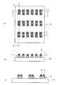
- FIG. 13 is an explanatory diagram showing an example of a wiring board on which bump electrodes are formed.
- FIG. 7A is a plan view of the wiring board 4 on which the bump electrodes 7 are formed.
- B is a sectional view taken along the line JJ of (a)
- (c) is a sectional view taken along the line KK of (a).
- D) is an enlarged view of a region R5 indicated by a broken line in (b).
- the wiring board 4 is provided with a plurality of electrode pads 4a (see FIG. 13D) corresponding to the LED electrodes 31a and 31b of the plurality of LEDs 3 arranged in a matrix.
- the conductive elastic protrusion 71 is formed on the electrode pad 4a (see FIG. 13D). Specifically, in step S21, a resist for a photo spacer is applied to the entire surface of the wiring board 4, and then exposed by using a photo mask and developed to pattern and form a protrusion on the electrode pad 4a. In step S21, a conductive film 72 of good conductivity such as gold or aluminum is formed on the projection and the electrode pad 4a by sputtering, vapor deposition or the like to form a conductive elastic projection 71.
- the bump electrode 7 including the elastic protrusion 71, the conductor film 72, and the electrode pad 4a is formed.
- the bump electrode 7 is specifically composed of an anode electrode 7a and a cathode electrode 7b corresponding to the LED electrodes 31a and 31b (see FIGS. 13A and 13C).
- the bump electrode 7 has, for example, a height (h 3 ) of 4 ⁇ m and a diameter (d) of 10 ⁇ m (see FIG. 13D).
- the elastic protrusion 71 may be a protrusion formed of a conductive photoresist in which conductive fine particles such as silver are added to the photoresist or a conductive photoresist containing a conductive polymer.
- a conductive photoresist is applied to the entire upper surface of the wiring substrate 4 with a predetermined thickness, and then exposed using a photomask and developed to form protrusions on the electrode pads as elastic protrusions. 71 is patterned.
- the bump electrode 7 is composed of the elastic protrusion 71 having conductivity and the electrode pad 4a. As described above, since the bump electrode 7 can be formed by applying the photolithography process, it is possible to secure high accuracy in position and shape.
- the second adhesive 8 is applied on the wiring board 4 on which the bump electrodes 7 are formed.
- the second adhesive 8 is, for example, a resin composition in which an insulating thermosetting resin is mixed with an adhesive material and a photosensitizer.
- the second adhesive 8 is a resin composition that develops an adhesive function and is cured by heating.
- the second adhesive 8 contains a photosensitizer, it has a photosensitivity function capable of patterning by ultraviolet rays. That is, the second adhesive 8 also functions as a photoresist.
- step S22 the second adhesive 8 is applied onto the wiring board 4 using a spin coater in the same manner as the application of the first adhesive (step S11).
- step S22 the wiring board 4 coated with the second adhesive 8 is pre-baked by a heating means such as a heater (not shown).
- the prebaking conditions are, for example, a heating temperature of 100° C. and a heating time of 5 minutes.
- step S23 the wiring board 4 coated with the second adhesive 8 is irradiated with ultraviolet (UV) light through a photomask.
- step S24 the wiring board 4 is immersed in a developing solution and washed.
- the second adhesive 8 is patterned around each bump electrode 7 (anode electrode 7a and cathode electrode 7b) in a predetermined arrangement by a photomask.
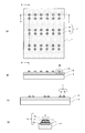
- FIG. 14 is an explanatory diagram showing a state in which the second adhesive is laminated on the wiring board.
- FIG. 3A is a plan view of the surface of the wiring board 4.
- (B) is a sectional view taken along line LL in (a)
- (c) is a sectional view taken along line MM in (a).
- FIG. 15 is an explanatory diagram showing the positional relationship between the second adhesive and the bump electrodes.
- FIG. 14A is an enlarged view of a main part (a portion marked with a reference numeral) of a region R6 indicated by a broken line in FIG.
- FIG. 14B is an enlarged view of the region R7 indicated by the broken line in FIG. (C) is a modification of (b).
- the second adhesive 8 surrounds the bump electrode 7 with a space. Further, as shown in FIG. 15A, the height (h 4 ) of the second adhesive 8 is set higher than the height (h 3 ) of the bump electrode 7. Height of the second adhesive 8 (h 4) the height of the bump electrode 7 (h 3) the ratio of P 2 (h 4 / h 3 ) , for example, preferably about 1.5. Therefore, in FIG. 15A, the height (h 3 ) of the bump electrode 7 is 4 ⁇ m and the height (h 4 ) of the second adhesive 8 is 6 ⁇ m, as an example.
- the bump electrode 7 is pressed, the first adhesive 6 is also deformed by the pressure so as to fill the gap in the space. By doing so, the bump electrode 7 (anode electrode 7a and cathode electrode 7b) is surely bonded with the first adhesive 6 before thermosetting.
- the second adhesive 8 leaves a space and surrounds the periphery of the bump electrode 7, it is not limited to the space having the shape as shown in FIG. 15B, but the shape as shown in FIG. 15C. It may be a space.
- the order of execution of the wafer processing (step S1) and the wiring board processing (step S2) shown in FIG. 5 may be interchanged.
- step S3 when the surface of the wafer 10 and the surface of the wiring substrate 4 are bonded together, a mechanism (not shown) capable of alignment is provided on the wafer 10 and the wiring substrate 4 in advance. Using the provided alignment marks (not shown). Align.
- FIG. 16 is a process diagram illustrating the process from the alignment to the bonding shown in FIG.
- FIG. 17 is a process diagram for explaining the process from pressing to peeling of the wafer shown in FIG.
- FIG. 16A is a diagram showing the alignment between the wafer 10 and the wiring board 4.
- step S3 the LED electrode 31a and the anode electrode 7a of the wiring substrate 4 are aligned so as to contact each other via the first adhesive 6, and the LED electrode 31b and the wiring are connected via the first adhesive 6.
- the substrate 4 is aligned so as to come into contact with the cathode electrode 7b.
- FIG. 16B illustrates a state where the first adhesive 6 and the second adhesive 8 are heated by the heater H.
- FIG. 18 is a graph showing the temperature characteristics of the viscosities of the first adhesive and the second adhesive.
- FIG. 18 shows the outline of the experimental results.
- the horizontal axis represents temperature (° C.), and the vertical axis represents arbitrary unit of viscosity (Pa).
- the first adhesive 6 and the second adhesive 8 used in this embodiment have the characteristic that the viscosity becomes the lowest at about 120°C.
- the first adhesive 6 and the second adhesive 8 may be adhesives having both thermoplasticity and thermosetting, 120° C. and It has the characteristic that it becomes the softest before and after.
- it is preferable that the first adhesive 6 and the second adhesive 8 are attached in the softest state and pressed. Therefore, the first adhesive 6 and the second adhesive 8 are heated to about 120° C., and the process proceeds to bonding (step S5).
- step S5 the wafer 10 and the wiring board 4 are bonded together based on the alignment mark described above.
- FIG. 16C is a diagram showing the bonding between the wafer 10 and the wiring board 4.
- the wafer 10 is lowered by an elevating mechanism (not shown) while the first adhesive 6 and the second adhesive 8 are heated to about 120° C., and the wiring substrate 4 and the wafer 10 are bonded to each other.
- the first adhesive 6 on one side and the anode electrode 7a of the wiring board 4 contact each other, and the first adhesive 6 on the other side and the cathode electrode 7b of the wiring board 4 contact each other. The state which abutted is illustrated.
- step S6 the wafer 10 is further lowered by the elevating mechanism to press the wafer 10 against the wiring substrate 4 at a predetermined pressure P.
- the LED electrodes 31a and 31b of the LEDs 3 on the wafer 10 and the bump electrodes 7 on the wiring board 4 are bonded together via the first adhesive 6 and pressed.
- FIG. 17A is a diagram showing a state in which the wafer 10 is pressed against the wiring board 4 with the pressure P.
- step S7 the first adhesive 6 and the second adhesive 8 are heated by the heater H in order to be further hardened.
- step S7 for example, the curing temperature is set to 230° C. and the heating time is set to 30 minutes to cure the first adhesive agent 6 and the second adhesive agent 8.
- the curing temperature may be set to 200° C. and the heating time may be set to 60 minutes.
- the curing temperature may be 180° C. and the heating time may be 90 minutes.
- FIG. 17B illustrates a state in which the first adhesive 6 and the second adhesive 8 are further heated using the heater H.
- step S8 the bonded wafer 10 and the wiring board 4 are cooled and returned to room temperature (for example, 25° C.), and then the wafer 10 is lifted by the elevating mechanism to move the wafer 10 to the wiring board 4 Peel from. As a result, the LED 3 is mounted on the wiring board 4.
- room temperature for example, 25° C.
- FIG. 19 is an explanatory diagram of the LED array substrate formed by peeling the wafer.
- FIG. 3A is a plan view of the LED array substrate 1.
- (B) is a sectional view taken along line NN of (a), and
- (c) is a sectional view taken along line OO of (a).
- the LED array substrate 1 is an example of a micro LED mounting structure as described above.
- step S9 for example, a transparent insulating photosensitive resin is applied onto the LED array substrate 1 shown in FIG. 19 by using a micro dispenser (not shown) under automatic control. Then, the flattening film 9 is formed by irradiating the photosensitive resin with ultraviolet (UV) light to cure it. That is, the flattening film 9 is laminated on the LED array substrate 1. In this case, all the LEDs 3 are covered with the flattening film 9. In this embodiment, since the photosensitive resin is applied so as to have a uniform height, the flattened film 9 having a flat plate shape is formed.
- UV ultraviolet
- FIG. 20 is an explanatory diagram of an LED array substrate on which a flattening film is laminated.
- FIG. 3A is a plan view of the LED array substrate 1 on which a flattening film is formed.
- (B) is a sectional view taken along the line PP of (a), and
- (c) is a sectional view taken along the line QQ of (a).
- 20A since the flattening film 9 is transparent, the light emitting surface 32 of each LED 3 can be seen.
- the flattening film 9 will be described later with reference to FIG.
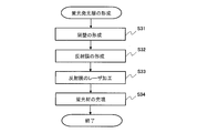
- FIG. 21 is a flowchart showing the steps of forming the fluorescent light emitting layer.
- FIG. 22 is a process diagram illustrating a process of forming a fluorescent light emitting layer. In the formation of the fluorescent light emitting layer (step S10), the processes from step S31 to step S34 shown in FIG. 22 are performed.
- step S31 the partition 12 is formed on the LED array substrate 1 on which the flattening film 9 is formed.
- FIG. 22A shows a state in which the partition wall 12 is provided on the LED array substrate 1 shown in FIG. 20B.
- step S31 for example, a transparent photosensitive resin for the partition wall 12 is applied, and then exposed using a photomask and developed to form the respective fluorescent material layers 11R, 11G, and 11B (see FIG. 22D).
- the opening 12a is provided in accordance with the above (see).
- the transparent partition wall 12 having a height-to-width aspect ratio of 3 or more is formed with a height of about 20 ⁇ m per minute.
- the photosensitive resin used is preferably a high aspect material such as SU-83000 manufactured by Nippon Kayaku Co., Ltd., for example.
- a film formation technique such as sputtering is applied from the side of the partition 12 formed on the LED array substrate 1 to form a predetermined reflection film 13 such as aluminum or aluminum alloy.
- the film is formed to a thickness.
- the reflection film 13 may be formed to have a predetermined thickness by plating.
- FIG. 22B shows a state after the reflective film 13 is formed.
- the unnecessary reflection film 13 is removed.
- the reflection film 13 covering the upper portion of the opening surrounded by the partition 12 is removed by laser irradiation suitable for laser processing of the reflection film 13.
- the laser irradiation removes the reflection film 13 in the region other than the side surface inside the opening.
- the second harmonic SHG: Second-Harmonic Generation
- the third harmonic TMG: Third-Harmonic Generation
- the fourth harmonic has a wavelength of 266 nm.
- FIG. 22C shows a state where the reflective film 13 is formed on the partition wall 12 after laser processing.
- step S34 in the filling of the fluorescent material (step S34), as the fluorescent material of RGB, a red fluorescent pigment is filled in the opening corresponding to red to form the fluorescent material layer 11R, and a green fluorescent pigment is filled in the opening corresponding to green.
- a fluorescent material layer 11G blue fluorescent dye is filled in the opening corresponding to blue to form the fluorescent material layer 11B.
- step S34 a resist containing the red fluorescent dye 14 is applied, and then exposed by using a photomask, developed, and baked, whereby the red fluorescent material is provided in the opening corresponding to red.
- the layer 11R is formed.
- the resist is obtained by mixing and dispersing the fluorescent dye 14a having a large particle diameter and the fluorescent dye 14b having a small particle diameter.
- step S34 the method of forming the red fluorescent material layer 11R in the opening corresponding to red is similarly applied to form the green fluorescent material layer 11G in the opening corresponding to green. Further, in step S34, the technique of forming the red fluorescent material layer 11R in the opening corresponding to red is similarly applied to form the blue fluorescent material layer 11B in the opening corresponding to blue.
- FIG. 22D is a diagram showing a state after filling the RGB fluorescent materials.
- the fluorescent light emitting layer 11 can be formed on the LED array substrate 1 as shown in FIG.
- FIG. 23 is an explanatory diagram showing the influence of the thickness of the flattening film on the light emission.
- the thickness (T) of the flattening film 9 indicates the distance from the bottom surface of the partition wall 12 to the light emitting surface 32 of the LED 3.
- the flattening film 9 may not have the thickness (T), or may have a predetermined thickness (see FIG. 23A).
- FIG. 23A shows a state in which the partition wall 12 is formed in the sectional view taken along the line PP of FIG. 20A.
- the thickness (T) is made larger than that in FIG. 23(a). That is, depending on the thickness (T) of the flattening film 9, light emitted from the light emitting surface 32 of the LED 3 may enter the adjacent fluorescent material layer. In this case, for example, when the light emission of the LED 3 located immediately below the adjacent fluorescent material layer is turned off (extinguished), the adjacent fluorescent material layer may also emit fluorescent light FL to cause color mixing (see FIG. 23(b)). ). Therefore, it is desirable that the thickness (T) of the flattening film 9 be optimized.
- FIG. 23C is an explanatory diagram for optimizing the thickness (T) of the flattening film.
- the thickness (T) of the flattening film 9 is obtained depending on parameters including the width D1 of the partition wall 12, the lateral width D2 of the LED 3, and the emission angle ( ⁇ ) of the light emitted from the light emitting surface 32 of the LED 3.
- the emission angle ( ⁇ ) of the light emitted from the light emitting surface 32 intersects with the horizontal line of the light emitting surface 32 and the vector of the arrow A indicating the light emitting direction in the cross-sectional view of FIG. Angle. That is, in the flattening film 9, the thickness (T) on the light emitting surface 32 is determined based on the light emission angle ( ⁇ ).
- the thickness (T) of the flattening film 9 is based on the parameters including the width D1 of the partition wall 12, the lateral width D2 of the LED 3, and the emission angle ( ⁇ ) of the light emitted from the light emitting surface 32 of the LED 3.
- the manufacturing method of the micro LED display of the present invention it is possible to manufacture the micro LED display including the micro LED mounting structure of the present invention as described above. As a result, it is possible to improve the yield due to a defective connection of the micro LED in the manufacturing stage of the micro LED display.
- the bump-free electrode wiring may be provided as the electrode portion on the surface of the wiring board 4.
- the bonding surface is small, so that soldering or anisotropic conductive film (ACF: Anisotropic Conductive Film) is used. ) Was difficult to bond.
- ACF Anisotropic Conductive Film
- the above embodiment is characterized in that the electrode surfaces are adhered to each other and the side surfaces of the LED 3 are adhered to each other, and a stable connection and a strong adhesive force can be obtained even for a minute micro LED like the LED 3.
- LED array substrate (micro LED mounting structure) 2... Fluorescent light emitting layer array 3... Micro LED 4... Wiring board 6... 1st adhesive agent 7... Bump electrode 8... 2nd adhesive agent 9... Flattening film 11... Fluorescent light emitting layer 21... Cell 31a, 31b... LED electrode 32... Light emission surface
Abstract
This MicroLED mounting structure comprises: a wiring board 4 that has, on one side thereof, electrode parts 7 arranged according to a predetermined array; and a microLED 3 that is provided so as to correspond to the positions of the electrode parts 7, that emits light of a specified spectrum from the ultraviolet wavelength band to the blue wavelength band, that has, on one surface of mutually opposed surfaces thereof, electrodes 31a, 31b which are electrically connected to the electrode parts 7, and that has, on another surface thereof, a light emission surface 32 which projects emitted light. The electrodes 31a, 31b and the electrode parts 7 are bonded via a conductive, thermosetting first adhesive 6. All or part of the peripheral lateral surface of the microLED 3 is enclosed and bonded by an insulating, thermosetting second adhesive 8. The microLED 3 is fixed to the wiring board via the second adhesive 8. Due to this configuration, provided is a means for reliably bonding and electrically connecting the electrodes of the microLED to the electrode parts of the wiring board and for reliably connecting the microLED to the wiring board.
Description
本発明は、マイクロLED(light emitting diode)を配線基板に実装するマイクロLED実装構造に関し、特にマイクロLEDの電極と配線基板の電極部との接着及び導通を確実に行なえると共に、マイクロLEDと配線基板との接続を確実に行なえるマイクロLED実装構造、そのマイクロLED実装構造を採用したマイクロLEDディスプレイ、及びマイクロLEDディスプレイの製造方法に係るものである。
The present invention relates to a micro LED mounting structure in which a micro LED (light emitting diode) is mounted on a wiring board, and in particular, the bonding and conduction between the electrodes of the micro LED and the electrode portion of the wiring board can be reliably performed, and the micro LED and wiring The present invention relates to a micro LED mounting structure that can be reliably connected to a substrate, a micro LED display using the micro LED mounting structure, and a method for manufacturing the micro LED display.
従来、ミクロンオーダーのサイズからなるマイクロLEDを画素としたフラットパネルディスプレイの製造工程においては、サファイア等の基板上に形成されたマイクロLEDを基板から剥離し、配線基板へ接続する必要がある。そこで、配線基板へのマイクロLEDの接続を容易にするための構造としては、マイクロLEDの電極と配線基板上に形成された電極配線とを当接させて周囲を接着剤層で固めたものが開示されている(例えば、特許文献1参照)。
Conventionally, in the manufacturing process of flat panel displays in which micro LEDs of micron order size are used as pixels, it is necessary to separate the micro LEDs formed on the substrate such as sapphire from the substrate and connect it to the wiring substrate. Therefore, as a structure for facilitating the connection of the micro LED to the wiring board, there is a structure in which the electrodes of the micro LED and the electrode wiring formed on the wiring board are brought into contact with each other and the periphery is solidified with an adhesive layer. It is disclosed (for example, see Patent Document 1).
しかし、上記接着剤層が絶縁性を有しているため、配線基板の電極配線とマイクロLEDの電極とを当接させて接着させる際、上記接着剤層が電極配線とマイクロLEDの電極との境界面に染み込む等の事象が発生した場合、導通が図られなくなるおそれがある。
However, since the adhesive layer has an insulating property, when the electrode wiring of the wiring board and the electrode of the micro LED are brought into contact with each other to be adhered, the adhesive layer separates the electrode wiring from the electrode of the micro LED. When an event such as seeping into the boundary surface occurs, there is a risk that conduction will not be achieved.
そこで、本発明は、このような問題点に対処し、マイクロLEDの電極と配線基板の電極部との接着及び導通を確実に行なえると共に、マイクロLEDと配線基板との接続を確実に行なえるマイクロLED実装構造、そのマイクロLED実装構造を採用したマイクロLEDディスプレイ、及びそのマイクロLEDディスプレイの製造方法を提供することを目的とする。
Therefore, the present invention addresses such a problem, and can reliably bond and electrically connect the electrode of the micro LED and the electrode portion of the wiring board, and securely connect the micro LED and the wiring board. It is an object of the present invention to provide a micro LED mounting structure, a micro LED display adopting the micro LED mounting structure, and a method for manufacturing the micro LED display.
上記目的を達成するために、本発明によるマイクロLED実装構造は、予め定められた配列に従って配設された電極部を片面に有する配線基板と、上記電極部の位置に対応して設けられ、紫外から青色波長帯までのうちで特定のスペクトルを有する光を発光し、相対向する面の一方の面上に上記電極部と導通接続する電極を有し、他方の面に光放出面を有するマイクロLEDと、を備え、上記マイクロLEDの電極と上記配線基板の電極部とは、導電性を有する熱硬化型の第1の接着剤を介して接着されており、上記マイクロLEDの周側面の一部又は全部が、絶縁性を有する熱硬化型の第2の接着剤で囲まれて接着されており、上記マイクロLEDが上記第2の接着剤を介して上記配線基板に固定されているものである。
In order to achieve the above-mentioned object, a micro LED mounting structure according to the present invention is provided with a wiring board having an electrode portion arranged on one side according to a predetermined arrangement and a position corresponding to the position of the electrode portion. To a blue wavelength band, it emits light having a specific spectrum, has an electrode that is conductively connected to the electrode portion on one of the opposite surfaces, and has a light emitting surface on the other surface. An LED is provided, and the electrode of the micro LED and the electrode portion of the wiring board are bonded to each other via a thermosetting first adhesive having conductivity. All or part of the micro LED is surrounded and adhered by an insulating thermosetting second adhesive, and the micro LED is fixed to the wiring board via the second adhesive. is there.
上記目的を達成するために、本発明によるマイクロLEDディスプレイは、フルカラー表示が可能なマイクロLEDディスプレイであって、予め定められた配列に従って配設された電極部を片面に有する配線基板に、上記電極部の位置に対応して、紫外から青色波長帯までのうちで特定のスペクトルを有する光を発光し、相対向する面の一方の面上に上記配線基板の電極部と導通接続する電極を有し、他方の面に光放出面を有するマイクロLEDを実装したLEDアレイ基板と、上記LEDアレイ基板上に、上記マイクロLEDから放出される光によって励起されることにより、光の三原色であるR(赤)、G(緑)、B(青)の対応色の蛍光に夫々波長変換する蛍光材を含む蛍光発光層を複数有する蛍光発光層アレイと、を備え、上記マイクロLEDの電極と上記配線基板の電極部とは、導電性を有する熱硬化型の第1の接着剤を介して接着されており、上記マイクロLEDの周側面の一部又は全部が、絶縁性を有する熱硬化型の第2の接着剤で囲まれて接着されており、上記マイクロLEDが上記第2の接着剤を介して上記配線基板に固定されているものである。
In order to achieve the above object, a micro LED display according to the present invention is a micro LED display capable of full color display, in which a wiring board having an electrode portion arranged according to a predetermined arrangement on one surface is provided with the electrode. Depending on the position of the part, it emits light having a specific spectrum in the ultraviolet to blue wavelength band, and has an electrode that is conductively connected to the electrode part of the wiring board on one of the opposite surfaces. Then, an LED array substrate having a micro LED having a light emitting surface on the other surface is mounted on the LED array substrate, and the three primary colors of light R( A fluorescent light emitting layer array having a plurality of fluorescent light emitting layers each containing a fluorescent material that converts wavelengths into fluorescent light of corresponding colors of red), G (green), and B (blue), and the electrodes of the micro LED and the wiring board. Of the micro LED is adhered via a first thermosetting adhesive having conductivity, and a part or all of the peripheral side surface of the micro LED has a second thermosetting type having an insulating property. The micro LED is surrounded and adhered to the wiring board, and is fixed to the wiring board via the second adhesive.
上記目的を達成するために、本発明によるマイクロLEDディスプレイの製造方法は、フルカラー表示が可能なマイクロLEDディスプレイの製造方法であって、紫外から青色波長帯までのうちで特定のスペクトルを有する光を発光し、相対向する面の一方の面上に電極を有し、他方の面に光放出面を有するマイクロLEDが予め定められた配列に従って表面に形成された透明基板に対して、上記電極上に導電性を有する熱硬化型の第1の接着剤をパターニングして積層する工程と、上記透明基板の裏面からレーザ光を照射することにより、上記透明基板の表面と上記マイクロLEDとの接合状態を、上記レーザ光の照射前と比較して弱くするレーザ加工を行なう工程と、予め定められた配列に従って配設された電極部を片面に有する配線基板に対して、上記マイクロLEDの周側面の一部又は全部を囲んで接着する、絶縁性を有する熱硬化型の第2の接着剤を、上記配線基板の電極部の周囲に空間を空けてパターニングして積層する工程と、上記透明基板上のマイクロLEDの電極と上記配線基板上の電極部とを、上記第1の接着剤を介して貼り合わせて加圧する工程と、上記第1の接着剤及び第2の接着剤を加熱により硬化させる工程と、上記マイクロLEDから上記透明基板を剥離して、上記マイクロLEDを上記配線基板に実装したLEDアレイ基板を形成する工程と、を含む。
In order to achieve the above-mentioned object, a method for manufacturing a micro LED display according to the present invention is a method for manufacturing a micro LED display capable of full color display, wherein a light having a specific spectrum from ultraviolet to blue wavelength band is emitted. On a transparent substrate on the surface of which a micro-LED that emits light and has an electrode on one surface of the opposite surface and a light emitting surface on the other surface is formed according to a predetermined arrangement, A step of patterning and laminating a thermosetting first adhesive having conductivity on the surface of the transparent substrate, and irradiating a laser beam from the back surface of the transparent substrate to bond the surface of the transparent substrate to the micro LED. A step of performing laser processing to weaken the laser beam compared to before irradiation with the laser beam, and a wiring board having an electrode portion arranged in accordance with a predetermined arrangement on one surface of the peripheral side surface of the micro LED. A step of patterning and laminating a thermosetting second adhesive having an insulating property, which surrounds a part or all of the adhesive and forms a space around the electrode part of the wiring board; Of the electrodes of the micro LED and the electrode portion on the wiring board are pasted together via the first adhesive to apply pressure, and the first adhesive and the second adhesive are cured by heating. And a step of peeling the transparent substrate from the micro LED to form an LED array substrate in which the micro LED is mounted on the wiring substrate.
本発明によるマイクロLED実装構造によれば、上記マイクロLEDの電極と上記配線基板の電極部とが導電性を有する上記第1の接着剤を介して接着される。これにより、上記マイクロLEDの電極と上記配線基板の電極部との接着及び導通を確実に行なうことができる。また、本発明によるマイクロLED実装構造によれば、絶縁性を有する上記第2の接着剤が上記第1の接着剤を積層した上記電極を含むマイクロLEDの周側面の一部又は全部を囲んで接着するので、上記マイクロLEDを上記第2の接着剤を介して上記配線基板に確実に固定させて接続することができる。
According to the micro LED mounting structure of the present invention, the electrode of the micro LED and the electrode portion of the wiring board are bonded via the first adhesive having conductivity. As a result, the electrodes of the micro LEDs and the electrode portions of the wiring board can be reliably bonded and conducted. Further, according to the micro LED mounting structure of the present invention, the second adhesive having an insulating property surrounds a part or all of the peripheral side surface of the micro LED including the electrode in which the first adhesive is laminated. Since they are adhered, the micro LED can be reliably fixed and connected to the wiring board via the second adhesive.
また、本発明によるマイクロLEDディスプレイによれば、本発明によるマイクロLED実装構造を含むので、上記マイクロLEDの電極と上記配線基板の電極部との接着及び導通を確実に行なうことができると共に、上記マイクロLEDを上記第2の接着剤を介して上記配線基板に確実に固定させて接続することができる。
Further, according to the micro LED display of the present invention, since the micro LED mounting structure of the present invention is included, the electrode of the micro LED and the electrode portion of the wiring board can be reliably bonded and conducted, and The micro LED can be securely fixed and connected to the wiring board via the second adhesive.
さらに、本発明によるマイクロLEDディスプレイの製造方法によれば、本発明によるマイクロLED実装構造を含むマイクロLEDディスプレイを製造することができる。
Furthermore, according to the method for manufacturing a micro LED display of the present invention, it is possible to manufacture a micro LED display including the micro LED mounting structure of the present invention.
以下、本発明の実施形態を添付図面に基づいて詳細に説明する。
[マイクロLEDディスプレイ]
図1は、本発明によるマイクロLEDディスプレイの実施形態を模式的に示す平面図である。このマイクロLEDディスプレイは、マイクロLEDとRGB蛍光体とを組み合わせて、フルカラー表示が可能なデバイスであって、LEDアレイ基板1と蛍光発光層アレイ2とを備えて成る。なお、本発明によるマイクロLEDディスプレイは、フラットディスプレイやフレキシブルディスプレイに適用可能である。このマイクロLEDディスプレイが、例えばフラットディスプレイに適用される場合、図1において、他の構成要素として、例えば保護ガラスの図示が省略されている。 Hereinafter, embodiments of the present invention will be described in detail with reference to the accompanying drawings.
[Micro LED display]
FIG. 1 is a plan view schematically showing an embodiment of a micro LED display according to the present invention. This micro LED display is a device capable of full color display by combining a micro LED and an RGB phosphor, and includes anLED array substrate 1 and a fluorescent light emitting layer array 2. The micro LED display according to the present invention can be applied to a flat display or a flexible display. When this micro LED display is applied to, for example, a flat display, illustration of a protective glass as another component is omitted in FIG. 1.
[マイクロLEDディスプレイ]
図1は、本発明によるマイクロLEDディスプレイの実施形態を模式的に示す平面図である。このマイクロLEDディスプレイは、マイクロLEDとRGB蛍光体とを組み合わせて、フルカラー表示が可能なデバイスであって、LEDアレイ基板1と蛍光発光層アレイ2とを備えて成る。なお、本発明によるマイクロLEDディスプレイは、フラットディスプレイやフレキシブルディスプレイに適用可能である。このマイクロLEDディスプレイが、例えばフラットディスプレイに適用される場合、図1において、他の構成要素として、例えば保護ガラスの図示が省略されている。 Hereinafter, embodiments of the present invention will be described in detail with reference to the accompanying drawings.
[Micro LED display]
FIG. 1 is a plan view schematically showing an embodiment of a micro LED display according to the present invention. This micro LED display is a device capable of full color display by combining a micro LED and an RGB phosphor, and includes an
LEDアレイ基板1は、マイクロLED3(以下、単に「LED3」という)を個別に発光させるものであって、図1に示すようにマトリクス状に配置された複数のLED3と、LED3を駆動する配線基板4とを含む。
The LED array substrate 1 is for individually emitting micro LEDs 3 (hereinafter, simply referred to as “LED3”), and includes a plurality of LEDs 3 arranged in a matrix as shown in FIG. 1 and a wiring substrate for driving the LEDs 3. Including 4 and.
蛍光発光層アレイ2は、LED3から放出された光(励起光)によって励起されて、光の三原色であるR(赤)、G(緑)、B(青)の対応色の蛍光に夫々波長変換する蛍光材を含む蛍光発光層を複数有するものである。蛍光発光層アレイ2は、複数の蛍光発光層11をマトリクス状に配置している。
The fluorescent light emitting layer array 2 is excited by the light (excitation light) emitted from the LED 3 and wavelength-converted into fluorescence of corresponding colors of R (red), G (green) and B (blue) which are the three primary colors of light. And a plurality of fluorescent light emitting layers containing the fluorescent material. The fluorescent light emitting layer array 2 has a plurality of fluorescent light emitting layers 11 arranged in a matrix.
本実施形態では、説明の便宜上、1画素に相当する3つのLED3と、各々のLED3上に設けられた蛍光材層11R、11G、11Bを含む1つの蛍光発光層11との組み合わせを1つのセル21とする。つまり、LEDアレイ基板1と蛍光発光層アレイ2とを組み合わせることにより、セル21の単位で取り扱うことができる。これにより、マイクロLEDディスプレイは、フルカラー表示を実現するための複数のセル21がマトリクス状に配置されたことになる。図1では、説明をわかりやすくするため、セル21が4行5列で配置されている。
In the present embodiment, for convenience of description, a combination of three LEDs 3 corresponding to one pixel and one fluorescent light emitting layer 11 including the fluorescent material layers 11R, 11G, and 11B provided on each LED 3 is one cell. 21. That is, by combining the LED array substrate 1 and the fluorescent light emitting layer array 2, the cells 21 can be handled as a unit. As a result, in the micro LED display, the plurality of cells 21 for realizing full-color display are arranged in a matrix. In FIG. 1, the cells 21 are arranged in 4 rows and 5 columns for easy understanding of the description.
蛍光発光層11は、赤色の蛍光色素を充填した蛍光材層11R、緑色の蛍光色素を充填した蛍光材層11G、青色の蛍光色素を充填した蛍光材層11Bを有している。これらの蛍光色素は、RGB蛍光体の一例である。
The fluorescent light emitting layer 11 has a fluorescent material layer 11R filled with a red fluorescent dye, a fluorescent material layer 11G filled with a green fluorescent dye, and a fluorescent material layer 11B filled with a blue fluorescent dye. These fluorescent dyes are examples of RGB phosphors.
本実施形態においては、例えば、短波長の光を発光するLED3とRGB蛍光体とを組み合わせてフルカラー表示を実現する方式を採用する。そのため、LED3は、特定のスペクトルを有する光を発光するものであり、窒化ガリウム(GaN)を主材料として製造される。具体的には、LED3は、紫外光発光ダイオード(UV-LED)であって、波長が例えば200nm~380nmの近紫外線を発光するLEDである。また、LED3は、波長が例えば380nm~500nmの青色光を発光するLEDであってもよい。波長が例えば200nm~380nmの近紫外線や波長が例えば380nm~500nmの青色光は、特定のスペクトルを有する光の一例に相当する。
In the present embodiment, for example, a method of realizing full-color display by combining the LED 3 that emits light of a short wavelength and the RGB phosphor is adopted. Therefore, the LED 3 emits light having a specific spectrum and is manufactured using gallium nitride (GaN) as a main material. Specifically, the LED 3 is an ultraviolet light emitting diode (UV-LED), and is an LED that emits near-ultraviolet light having a wavelength of, for example, 200 nm to 380 nm. Further, the LED 3 may be an LED that emits blue light having a wavelength of, for example, 380 nm to 500 nm. Near-ultraviolet light having a wavelength of, for example, 200 nm to 380 nm and blue light having a wavelength of, for example, 380 nm to 500 nm correspond to an example of light having a specific spectrum.
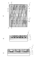
図2は、本発明によるマイクロLED実装構造を示す説明図である。ここで、LEDアレイ基板1は、本発明によるマイクロLED実装構造の一例である。図2(a)は、図1に示す破線R1で囲まれた領域において、LEDアレイ基板1のA-A線断面図を示している。また、図2(b)は、図1に示す破線R1で囲まれた領域において、LEDアレイ基板1のB-B線断面図を示している。図2(c)は、図2(a)に示す破線R2で囲まれているLEDアレイ基板1の要部拡大図であり、図2(d)は、図2(b)に示す破線R3で囲まれているLEDアレイ基板1の要部拡大図である。
FIG. 2 is an explanatory view showing a micro LED mounting structure according to the present invention. Here, the LED array substrate 1 is an example of a micro LED mounting structure according to the present invention. FIG. 2A shows a sectional view taken along the line AA of the LED array substrate 1 in the region surrounded by the broken line R1 shown in FIG. 2B is a sectional view taken along line BB of the LED array substrate 1 in the area surrounded by the broken line R1 shown in FIG. 2C is an enlarged view of a main part of the LED array substrate 1 surrounded by a broken line R2 shown in FIG. 2A, and FIG. 2D is a broken line R3 shown in FIG. 2B. It is a principal part enlarged view of the LED array substrate 1 enclosed.
LEDアレイ基板1は、図2(a)~(d)に示すとおり、ベース基板5上に配線基板4を有し、配線基板4上にLED3が接続され、さらに平坦化膜9が積層された構造を有している。そして、配線基板4とLED3とは、後述する第1の接着剤6及び第2の接着剤8により、機械的な接続及び電気的な接続が良好に実現されている。
As shown in FIGS. 2A to 2D, the LED array substrate 1 has a wiring substrate 4 on a base substrate 5, the LEDs 3 are connected on the wiring substrate 4, and a flattening film 9 is further laminated. It has a structure. Then, the wiring board 4 and the LED 3 are excellently realized by a first adhesive 6 and a second adhesive 8, which will be described later, in a mechanical connection and an electrical connection.
LED3は、図2(d)に示すとおり、レーザリフトオフ用の剥離層、発光層等の複数の階層を含む化合物半導体30を有している。LED3は、化合物半導体30において、一方の面上の予め定められた位置に発光用のLED電極31a、31bを有し、他方の面に光源(発光層)からの光を放出する光放出面32が形成されている。
As shown in FIG. 2D, the LED 3 has a compound semiconductor 30 including a plurality of layers such as a peeling layer for laser lift-off and a light emitting layer. The LED 3 has LED electrodes 31a and 31b for light emission at a predetermined position on one surface of the compound semiconductor 30, and a light emitting surface 32 for emitting light from a light source (light emitting layer) on the other surface. Are formed.
レーザリフトオフは、例えば、サファイア基板の一方の面に形成されたLEDに対して、サファイア基板の他方の面からパルス発振によるレーザ光を照射し、各々のLEDをサファイア基板から剥離させる手段である。具体的には、レーザリフトオフでは、剥離させたい箇所の界面領域(例えば剥離層)にレーザ光をフォーカスして照射することによって、例えばGaNの窒素が気化する現象に伴って、界面領域でLEDがサファイア基板から剥離される。レーザリフトオフを行なう装置(図示省略)によって、レーザリフトオフを行なう場合、例えば、固体UV(Ultra Violet:紫外線)領域のYAGレーザ発振器により、第4高調波(FHG:Fourth-Harmonic Generation)である波長266nmのピコ秒パルスレーザを使用することが好ましい。
Laser lift-off is, for example, a means of irradiating an LED formed on one surface of a sapphire substrate with laser light by pulse oscillation from the other surface of the sapphire substrate to separate each LED from the sapphire substrate. Specifically, in laser lift-off, by focusing and irradiating a laser beam on an interface region (for example, a peeling layer) at a portion to be peeled off, for example, due to a phenomenon that nitrogen of GaN is vaporized, an LED is emitted in the interface region. It is separated from the sapphire substrate. When laser lift-off is performed by a device (not shown) for performing laser lift-off, for example, a YAG laser oscillator in the solid-state UV (Ultra Violet) region uses a fourth harmonic (FHG: Fourth-Harmonic Generation) wavelength of 266 nm. It is preferable to use a picosecond pulsed laser.
但し、本実施形態では、レーザリフトオフを行なう装置を利用して、レーザパワー、レーザ光の照射領域、パルス照射に基づく照射回数等のパラメータを調節することによって、サファイア等の透明基板であるウエハ10(図6参照)をLED3から剥離させるのではなく、ウエハ10をLED3からは剥がれやすくしている点を特徴としている。詳細は、図9~図11を用いて後述する。
However, in the present embodiment, the wafer 10 which is a transparent substrate such as sapphire is adjusted by adjusting parameters such as laser power, a laser beam irradiation region, and the number of times of irradiation based on pulse irradiation using a device for performing laser lift-off. (See FIG. 6) is not peeled from the LED 3, but the wafer 10 is easily peeled from the LED 3. Details will be described later with reference to FIGS. 9 to 11.
配線基板4は、例えば、フレキシブルプリント配線基板(FPC:Flexible Printed Circuits)であって、絶縁性を有するベースフィルム(例えば、ポリイミド)と、電気回路を形成した配線層とからなるフィルム状の基板である。配線基板4は、予め定められた配列に従って片面に配設された導通接続用のバンプ電極7を有する。なお、配線基板4には、外部に設けられた駆動回路(図示省略)から複数のLED3の夫々に点灯及び消灯の駆動電流を供給することができるように配線が設けられている。ベース基板5は、LED3を実装した配線基板4を支持するものであって、例えば、石英ガラス等の透明な基板である。
The wiring board 4 is, for example, a flexible printed wiring board (FPC: Flexible Printed Circuits), and is a film-like board including an insulating base film (for example, polyimide) and a wiring layer on which an electric circuit is formed. is there. The wiring board 4 has bump electrodes 7 for conductive connection arranged on one surface in accordance with a predetermined arrangement. Wiring is provided on the wiring board 4 so that a driving circuit (not shown) provided outside can supply a driving current for turning on and off to each of the plurality of LEDs 3. The base substrate 5 supports the wiring substrate 4 on which the LEDs 3 are mounted, and is a transparent substrate such as quartz glass.
第1の接着剤6は、LED電極31a、31bと、バンプ電極7との接着及び導通を確実なものとするものである。第1の接着剤6は、各々のLED3のLED電極面上に積層され、導電性を有する熱硬化型の接着剤等を含む樹脂組成物である。
The first adhesive 6 ensures adhesion and conduction between the LED electrodes 31a and 31b and the bump electrodes 7. The first adhesive 6 is a resin composition that is laminated on the LED electrode surface of each LED 3 and includes a thermosetting adhesive having conductivity and the like.
バンプ電極7は、電極部の一例であって、配線基板4上に設けられ、第1の接着剤6を介してLED3のLED電極31a、31b(図2(d)参照)と接続して導通可能となる電極である。そして、バンプ電極7は、例えば導電性を有し、加圧により弾性変形するものである。これにより、LED3のLED電極31a、31bと配線基板4との接続がより確実になる。
The bump electrode 7 is an example of an electrode portion, is provided on the wiring board 4, and is electrically connected to the LED electrodes 31a and 31b (see FIG. 2D) of the LED 3 via the first adhesive 6. It is a possible electrode. The bump electrode 7 has, for example, conductivity and is elastically deformed by applying pressure. As a result, the connection between the LED electrodes 31a and 31b of the LED 3 and the wiring board 4 becomes more reliable.
第2の接着剤8は、配線基板4上に設けられ、第1の接着剤6を積層したLED電極31a、31bを含むLED3の周側面の一部又は全部を囲んで接着するものであって、絶縁性を有する熱硬化型の接着剤等を含む樹脂組成物である。
The second adhesive 8 is provided on the wiring board 4 and is adhered so as to surround part or all of the peripheral side surface of the LED 3 including the LED electrodes 31a and 31b in which the first adhesive 6 is laminated. A resin composition containing a thermosetting adhesive or the like having an insulating property.
平坦化膜9は、LED3の光放出面32を含む領域に積層されており、平板状に形成された膜である。平坦化膜9は、光放出面32から放出される光の射出角度に基づいて、光放出面32上の厚みが定められているものである。詳細は、図20、図23を用いて後述する。
The flattening film 9 is a film that is laminated in a region including the light emitting surface 32 of the LED 3 and has a flat plate shape. The thickness of the flattening film 9 is determined on the light emitting surface 32 based on the emission angle of the light emitted from the light emitting surface 32. Details will be described later with reference to FIGS.
そして、LEDアレイ基板1は、上述した構成において、LED3と配線基板4との接続に際して、各々のLED3を、第1の接着剤6を介してバンプ電極7に押し付けた状態で、第1の接着剤6及び第2の接着剤8を加熱により硬化させたものである。
Then, in the LED array substrate 1 having the above-described configuration, when the LEDs 3 and the wiring substrate 4 are connected, each LED 3 is pressed against the bump electrode 7 via the first adhesive 6, and the first bonding is performed. The agent 6 and the second adhesive 8 are cured by heating.
すなわち、LED3のLED電極31a、31bと配線基板4のバンプ電極7とは、第1の接着剤6を介して接着されている。具体的には、後述するように、LED電極31aとバンプ電極7(図13に示すアノード電極7a)とは、第1の接着剤6を介して接着されている。また、LED電極31bとバンプ電極7(図13に示すカソード電極7b)とは、第1の接着剤6を介して接着されている。さらに、LED3の周側面の一部が、第2の接着剤8で囲まれて接着されており、各々のLED3が第2の接着剤8を介して配線基板4に固定されている。なお、LED3の周側面の全部が、第2の接着剤8で囲まれて接着されるようにしてもよい。
That is, the LED electrodes 31a and 31b of the LED 3 and the bump electrodes 7 of the wiring board 4 are bonded together via the first adhesive 6. Specifically, as described later, the LED electrode 31a and the bump electrode 7 (anode electrode 7a shown in FIG. 13) are adhered to each other via the first adhesive 6. Further, the LED electrode 31b and the bump electrode 7 (cathode electrode 7b shown in FIG. 13) are adhered to each other via the first adhesive 6. Further, a part of the peripheral side surface of the LED 3 is surrounded and adhered by the second adhesive agent 8, and each LED 3 is fixed to the wiring board 4 via the second adhesive agent 8. The entire peripheral side surface of the LED 3 may be surrounded and adhered by the second adhesive 8.
図3は、セルの一例を示す説明図である。図4は、図3に示すセルの詳細な説明図である。図3(a)は、図1に示すセル21の平面図を示し、図3(b)は、図3(a)に示すC-C線断面図である。なお、図3(b)において、セル21は配線基板4及びベース基板5を含まない。蛍光発光層11は、LED3の光放出面32から放出された光(励起光)によって、赤色、緑色、青色の蛍光色素(蛍光材の一例)がフルカラー表示を実現するための赤(R)、緑(G)、青(B)の蛍光に夫々波長変換するものである。具体的には、蛍光発光層11は、励起光によって、各蛍光材層11R、11G、11Bの蛍光色素が励起状態に遷移し、その後、基底状態に戻るときに、各蛍光材によって各々波長変換された赤(R)、緑(G)、青(B)の可視スペクトルに相当する蛍光を発光する。これらの蛍光材層11R、11G、11Bは反射膜13を表面に有する隔壁12で区画されている。
FIG. 3 is an explanatory diagram showing an example of a cell. FIG. 4 is a detailed explanatory diagram of the cell shown in FIG. 3A is a plan view of the cell 21 shown in FIG. 1, and FIG. 3B is a sectional view taken along the line CC shown in FIG. 3A. In FIG. 3B, the cell 21 does not include the wiring substrate 4 and the base substrate 5. The fluorescent light emitting layer 11 uses red light (R) for realizing full-color display of red, green, and blue fluorescent dyes (an example of a fluorescent material) by light (excitation light) emitted from the light emitting surface 32 of the LED 3. The wavelengths are converted into green (G) and blue (B) fluorescence, respectively. Specifically, the fluorescent light emitting layer 11 causes the fluorescent dyes of the respective fluorescent material layers 11R, 11G, and 11B to transition to an excited state by excitation light, and then, when the fluorescent dyes return to the ground state, the respective fluorescent materials convert wavelengths. The emitted red (R), green (G), and blue (B) corresponding to the visible spectrum emits fluorescence. These fluorescent material layers 11R, 11G, and 11B are partitioned by partition walls 12 having a reflective film 13 on the surface.
図4には、セル21のより詳細な構成が示されており、蛍光発光層11は、LEDアレイ基板1上に設けられている。ここで、蛍光発光層11の蛍光材層11Rは、レジスト膜中にミクロンサイズの粒子径の蛍光色素14aと、ナノサイズの粒子径の蛍光色素14bとを混合、分散させたものである。また、蛍光材層11Gは、蛍光材層11Rと同様、ミクロンサイズの粒子径の蛍光色素14cと、ナノサイズの粒子径の蛍光色素14dとを混合、分散させたものである。さらに、蛍光材層11Bは、蛍光材層11Rと同様、ミクロンサイズの粒子径の蛍光色素14eと、ナノサイズの粒子径の蛍光色素14fとを混合、分散させたものである。このように、粒子径の異なる蛍光色素を用いることにより、ナノサイズの粒子径の蛍光色素が、蛍光色素の充填率の低下による励起光の漏れ光を防ぐと共に、ミクロンサイズの粒子径の蛍光色素が発光効率を向上させることができる。
A more detailed structure of the cell 21 is shown in FIG. 4, and the fluorescent light emitting layer 11 is provided on the LED array substrate 1. Here, the fluorescent material layer 11R of the fluorescent light emitting layer 11 is formed by mixing and dispersing a fluorescent dye 14a having a particle size of micron size and a fluorescent dye 14b having a particle size of nanosize in a resist film. Further, the fluorescent material layer 11G is formed by mixing and dispersing a fluorescent dye 14c having a micron-sized particle diameter and a fluorescent pigment 14d having a nano-sized particle diameter, like the fluorescent material layer 11R. Further, like the fluorescent material layer 11R, the fluorescent material layer 11B is formed by mixing and dispersing a fluorescent dye 14e having a particle size of micron size and a fluorescent dye 14f having a particle size of nano size. As described above, by using fluorescent dyes having different particle diameters, the fluorescent dyes with nano-sized particles can prevent the leakage of excitation light due to the decrease in the packing ratio of the fluorescent dyes, and the fluorescent dyes with micron-sized particles can be used. Can improve the luminous efficiency.
また、隔壁12は、遮光壁の一例であって、蛍光材層11R、11G、11Bを互いに隔てるものである。隔壁12は、例えば透明な感光性樹脂で形成されている。本実施形態では、例えば、蛍光材層11R内において、蛍光色素14bよりも粒子径が大きい蛍光色素14aの充填率を上げるためには、隔壁12として、高さ対幅のアスペクト比が3以上を可能とする高アスペクト材料を使用するのが望ましい。蛍光材層11G、11Bも同様である。このような高アスペクト材料としては、一例として日本化薬株式会社製のSU-8 3000のフォトレジストがある。
Further, the partition wall 12 is an example of a light shielding wall, and separates the fluorescent material layers 11R, 11G, and 11B from each other. The partition wall 12 is formed of, for example, a transparent photosensitive resin. In the present embodiment, for example, in the fluorescent material layer 11R, in order to increase the filling rate of the fluorescent dye 14a having a particle size larger than that of the fluorescent dye 14b, the partition wall 12 has an aspect ratio of height to width of 3 or more. It is desirable to use high aspect materials that allow. The same applies to the fluorescent material layers 11G and 11B. An example of such a high aspect material is SU-83000 photoresist manufactured by Nippon Kayaku Co., Ltd.
隔壁12の表面には、図4に示すように、反射膜13が設けられている。この反射膜13は、励起光と蛍光FLとが隔壁12を透過して隣接する他の蛍光材層内に入射するのを防止するものである。この蛍光FLは、各蛍光材層11R、11G、11Bの各蛍光色素が励起光により励起されることにより、発光する。反射膜13は、励起光及び蛍光FLを十分に遮断できる厚みで形成されている。この場合、反射膜13としては、励起光及び蛍光FLを反射し易いアルミニウムやアルミ合金等の薄膜が好適である。
A reflective film 13 is provided on the surface of the partition wall 12, as shown in FIG. The reflective film 13 prevents the excitation light and the fluorescent light FL from passing through the partition wall 12 and entering into another adjacent fluorescent material layer. This fluorescent light FL emits light when each fluorescent dye of each fluorescent material layer 11R, 11G, and 11B is excited by excitation light. The reflective film 13 is formed with a thickness that can sufficiently block the excitation light and the fluorescent light FL. In this case, the reflection film 13 is preferably a thin film of aluminum or aluminum alloy that easily reflects the excitation light and the fluorescent light FL.
蛍光発光層11は、隔壁12に向かう励起光をアルミニウム等の反射膜13で反射させ、各蛍光材層11R、11G、11Bの発光に利用することができる。そのため、各蛍光材層11R、11G、11Bの発光効率は、向上する。但し、隔壁12の表面に被着される薄膜は、励起光及び蛍光FLを反射する反射膜13に限られず、励起光及び蛍光FLを吸収するものであってもよい。
The fluorescent light emitting layer 11 can be used to emit light from the fluorescent material layers 11R, 11G, and 11B by reflecting the excitation light toward the partition wall 12 with the reflective film 13 such as aluminum. Therefore, the luminous efficiency of each of the fluorescent material layers 11R, 11G, and 11B is improved. However, the thin film deposited on the surface of the partition wall 12 is not limited to the reflective film 13 that reflects the excitation light and the fluorescence FL, and may be one that absorbs the excitation light and the fluorescence FL.
以上、本発明のマイクロLEDディスプレイの構成について説明した。ここで、本発明によるマイクロLED実装構造によれば、各々のLED3のLED電極31a、31bとバンプ電極7とが導電性を有する第1の接着剤6を介して接続され、LED3の周側面の一部が、絶縁性を有する第2の接着剤で囲まれて接着されており、LED3がその第2の接着剤を介して配線基板4に固定されている。これにより、本発明によるマイクロLED実装構造は、LED3のLED電極31a、31bと配線基板4のバンプ電極7との接着及び導通を確実に行なうことができると共に、LED3を第2の接着剤を介して配線基板4に確実に固定させて接続することができる。つまり、本発明によるマイクロLED実装構造は、LED3と配線基板4との電気的及び機械的接続を確実に行なうことができる。
The configuration of the micro LED display of the present invention has been described above. Here, according to the micro LED mounting structure of the present invention, the LED electrodes 31a and 31b of each LED 3 and the bump electrode 7 are connected via the first adhesive 6 having conductivity, and the bumps 7 are attached to the peripheral side surface of the LED 3. A part of the LED 3 is surrounded and adhered by a second adhesive having an insulating property, and the LED 3 is fixed to the wiring board 4 via the second adhesive. As a result, in the micro LED mounting structure according to the present invention, the LED electrodes 31a and 31b of the LED 3 and the bump electrodes 7 of the wiring board 4 can be reliably bonded and conducted, and the LED 3 is bonded via the second adhesive. The wiring board 4 can be securely fixed and connected. That is, in the micro LED mounting structure according to the present invention, the electrical and mechanical connection between the LED 3 and the wiring board 4 can be reliably performed.
また、本発明のマイクロLEDディスプレイによれば、上記のマイクロLED実装構造としてLEDアレイ基板1を有するので、上記LED3と上記配線基板4との電気的及び機械的接続を確実に行なうことができる。そして、外部に設けられた駆動回路から駆動電流が配線基板4に供給されることにより、本発明のマイクロLEDディスプレイはフルカラー表示が可能となる。
Further, according to the micro LED display of the present invention, since the LED array substrate 1 is provided as the micro LED mounting structure, it is possible to surely perform the electrical and mechanical connection between the LED 3 and the wiring substrate 4. Then, by supplying a drive current to the wiring board 4 from a drive circuit provided outside, the micro LED display of the present invention can perform full color display.
[マイクロLEDディスプレイの製造方法]
次に、このように構成されたマイクロLEDディスプレイの製造方法について説明する。
図5は、本発明に係るマイクロLEDディスプレイの製造方法の工程を示すフローチャートである。 [Method for manufacturing micro LED display]
Next, a method of manufacturing the micro LED display thus configured will be described.
FIG. 5 is a flowchart showing steps of the method for manufacturing a micro LED display according to the present invention.
図6は、ウエハの一例を示す説明図である。(a)は、ウエハ10の平面図である。(b)は、(a)のD-D線断面図であり、(c)は、(a)のE-E線断面図である。本実施形態では、説明をわかりやすくするため、一方の面(表面)上に予め定められた間隔でマトリクス状(3行6列)に配置された複数のLED3を有するウエハ10を用いて、マイクロLEDディスプレイの製造方法について説明をする。なお、複数のLED3は、例えばMOCVD(Metal Organic Chemical Vapor Deposition)等の結晶成長プロセスによりウエハ10の一方の面上に形成される。
FIG. 6 is an explanatory diagram showing an example of a wafer. FIG. 3A is a plan view of the wafer 10. (B) is a DD line sectional view of (a), (c) is a EE line sectional view of (a). In the present embodiment, in order to make the description easy to understand, a wafer 10 having a plurality of LEDs 3 arranged in a matrix (3 rows and 6 columns) at a predetermined interval on one surface (front surface) is used to A method for manufacturing the LED display will be described. The plurality of LEDs 3 are formed on one surface of the wafer 10 by a crystal growth process such as MOCVD (Metal Organic Chemical Vapor Deposition).
図6において、LED3は、例えば、列方向(y方向)にはW1のピッチの間隔が設けられ、行方向(x方向)にはW2のピッチの間隔が設けられるように配置されている。W1とW2との比率P1(W2/W1)は、図6に示す配置では、例えば3程度が好ましい。そのため、例えば、W1のピッチは50μm、W2のピッチは150μmとしている。また、LED3のサイズは、一例として、縦(a)=50μm、横(b)=16μmとしている。また、高さ(h1)については、例えば数μm~30μm程度のサイズを対象とすることができる。
In FIG. 6, the LEDs 3 are arranged, for example, with a pitch of W 1 in the column direction (y direction) and with a pitch of W 2 in the row direction (x direction). .. The ratio P 1 (W 2 /W 1 ) between W 1 and W 2 is preferably about 3 in the arrangement shown in FIG. Therefore, for example, the pitch of W 1 is 50 μm and the pitch of W 2 is 150 μm. The size of the LED 3 is, for example, vertical (a)=50 μm and horizontal (b)=16 μm. As for the height (h 1 ), for example, a size of several μm to 30 μm can be targeted.
(ウエハの加工)
図7は、ウエハの加工の工程を示すフローチャートである。ウエハの加工(工程S1)では、図7に示す工程S11から工程S14までの処理を行なう。ここで、ウエハの加工(工程S1)では、フォトマスク(図示省略)を使用したフォトリソグラフィー技術を適用して、ウエハ10に導電性及び感光性を有する熱硬化型の第1の接着剤6を塗布する。具体的には、ウエハの加工(工程S1)では、露光、現像によって、パターニングすることにより、LED電極31a、31b上に第1の接着剤6が積層される。以下、詳細を説明する。 (Processing of wafer)
FIG. 7 is a flowchart showing the steps of wafer processing. In the wafer processing (step S1), the processes from step S11 to step S14 shown in FIG. 7 are performed. Here, in the processing of the wafer (step S1), a photolithography technique using a photomask (not shown) is applied to apply the thermosettingfirst adhesive 6 having conductivity and photosensitivity to the wafer 10. Apply. Specifically, in the wafer processing (step S1), the first adhesive 6 is laminated on the LED electrodes 31a and 31b by patterning by exposure and development. The details will be described below.
図7は、ウエハの加工の工程を示すフローチャートである。ウエハの加工(工程S1)では、図7に示す工程S11から工程S14までの処理を行なう。ここで、ウエハの加工(工程S1)では、フォトマスク(図示省略)を使用したフォトリソグラフィー技術を適用して、ウエハ10に導電性及び感光性を有する熱硬化型の第1の接着剤6を塗布する。具体的には、ウエハの加工(工程S1)では、露光、現像によって、パターニングすることにより、LED電極31a、31b上に第1の接着剤6が積層される。以下、詳細を説明する。 (Processing of wafer)
FIG. 7 is a flowchart showing the steps of wafer processing. In the wafer processing (step S1), the processes from step S11 to step S14 shown in FIG. 7 are performed. Here, in the processing of the wafer (step S1), a photolithography technique using a photomask (not shown) is applied to apply the thermosetting
第1の接着剤の塗布(工程S11)では、LED3を配置しているウエハ10の面上に第1の接着剤6を塗布する。第1の接着剤6は、例えば、絶縁性の熱硬化性樹脂に、導電材料と、接着材料と、感光剤とを配合した樹脂組成物である。第1の接着剤6は、加熱することにより接着機能を発現して硬化する樹脂組成物である。接着材料は、例えば熱硬化型のエポキシ系の樹脂であってもよい。
In the application of the first adhesive (step S11), the first adhesive 6 is applied on the surface of the wafer 10 on which the LEDs 3 are arranged. The first adhesive 6 is, for example, a resin composition in which an electrically conductive material, an adhesive material, and a photosensitizer are mixed with an insulating thermosetting resin. The first adhesive 6 is a resin composition that develops an adhesive function and is cured by heating. The adhesive material may be, for example, a thermosetting epoxy resin.
また、第1の接着剤6には、導電材料として、例えば、10nm~1.0μm以下の範囲の粒子径から選択された微粒子のカーボンが配合され、導電性の機能が付加されたものである。本実施形態では、一例として、0.5μm~1.0μm程度の微粒子のカーボンを用いている。
Further, the first adhesive 6 contains, as a conductive material, for example, fine carbon particles selected from a particle diameter in the range of 10 nm to 1.0 μm, and has a conductive function added. .. In the present embodiment, as an example, fine particles of carbon of about 0.5 μm to 1.0 μm are used.
さらに、第1の接着剤6は、感光剤が配合されているため、紫外線によりパターニング形成が可能な感光性の機能が付加されたものである。すなわち、この第1の接着剤6は、フォトレジストとしても機能する。なお、絶縁性の熱硬化性樹脂自体が、接着機能を有する場合には、第1の接着剤6は、導電材料と感光剤とを配合した樹脂組成物であってよいし、さらに接着力を高めるために、接着材料を配合してもよい。
Furthermore, since the first adhesive 6 contains a photosensitizer, it has a photosensitivity function capable of patterning by ultraviolet rays. That is, the first adhesive 6 also functions as a photoresist. When the insulative thermosetting resin itself has an adhesive function, the first adhesive 6 may be a resin composition in which a conductive material and a photosensitizer are mixed, and the adhesive strength is further increased. Adhesive materials may be included to enhance.
ここで、導電材料は、上記のカーボンに限られず、金属の微粒子を採用してもよい。金属の微粒子としては、例えば銀(Ag)であることが好ましい。但し、ニッケル(Ni)、銅(Cu)、アルミニウム(Al)、金(Au)等、用途に応じて採用してもよい。そして、導電材料は、例えば、金属の粒子径が10nm程度の金属ナノ粒子から1.0μm以下の金属の微粒子までのうちから、適用可能なものを選択してもよい。
Here, the conductive material is not limited to the above-mentioned carbon, and metal fine particles may be adopted. The fine metal particles are preferably silver (Ag), for example. However, nickel (Ni), copper (Cu), aluminum (Al), gold (Au) or the like may be adopted depending on the application. Then, as the conductive material, for example, an applicable material may be selected from metal nanoparticles having a metal particle diameter of about 10 nm to metal fine particles having a particle diameter of 1.0 μm or less.
工程S11では、例えば、フォトリソグラフィー技術で使用されるスピンコータ(図示省略)を用いて、LED3を配置しているウエハ10の面上に第1の接着剤6を塗布する。スピンコータは、均一な塗布を実現するための装置である。具体的には、工程S11では、第1の接着剤6をフォトレジストとして、ウエハ10に滴下し、ウエハ10を予め定めた回転数、回転時間を設定することにより、ウエハ10の面上に第1の接着剤6が塗布される。なお、工程S11では、一定の膜厚に塗布する手段として、バーコーターを適用してもよい。そして、工程S11では、第1の接着剤6が塗布されたウエハ10を、ヒータ(図示省略)等の加熱手段により、プリベークする。プリベークの条件は、例えば、加熱温度を100℃とし、加熱時間を1分とする。
In step S11, the first adhesive 6 is applied onto the surface of the wafer 10 on which the LEDs 3 are arranged, for example, using a spin coater (not shown) used in photolithography technology. The spin coater is a device for realizing uniform coating. Specifically, in step S11, the first adhesive 6 is dropped onto the wafer 10 as a photoresist, and the wafer 10 is set on the surface of the wafer 10 by setting a predetermined rotation speed and rotation time. Adhesive 6 of No. 1 is applied. In step S11, a bar coater may be applied as a means for applying a uniform film thickness. Then, in step S11, the wafer 10 coated with the first adhesive 6 is pre-baked by a heating means such as a heater (not shown). The prebaking conditions are, for example, a heating temperature of 100° C. and a heating time of 1 minute.
露光(工程S12)では、第1の接着剤6を塗布したウエハ10へ、フォトマスクを介して紫外(UV)光を照射する。現像(工程S13)では、ウエハ10を現像液へ浸して洗浄する。これにより、LED電極31a、31b上に第1の接着剤6が積層される。
In the exposure (step S12), the wafer 10 coated with the first adhesive 6 is irradiated with ultraviolet (UV) light through a photomask. In the development (step S13), the wafer 10 is immersed in a developing solution for cleaning. As a result, the first adhesive 6 is laminated on the LED electrodes 31a and 31b.
図8は、LED電極上に第1の接着剤が積層された状態を示す説明図である。(a)は、ウエハ10の表面の平面図である。(b)は、(a)のF-F線断面図であり、(c)は、(a)のG-G線断面図である。LED電極31a、31b上に積層された第1の接着剤6の膜厚(h2)は、一例として、2μmとしている。
FIG. 8 is an explanatory diagram showing a state in which the first adhesive is laminated on the LED electrodes. FIG. 3A is a plan view of the surface of the wafer 10. (B) is the FF line sectional view of (a), (c) is the GG line sectional view of (a). The film thickness (h 2 ) of the first adhesive 6 laminated on the LED electrodes 31a and 31b is, for example, 2 μm.
レーザ加工(工程S14)では、ウエハ10とLED3との界面に対して、ウエハ10の裏面からレーザ光Lをフォーカスして照射する。具体的には、工程S14では、ウエハ10の裏面からレーザ光Lを照射することにより、ウエハ10の表面に形成されたLED3の接合状態を、レーザ光Lの照射前と比較して弱くするレーザ加工を行なう。この場合、工程S14では、ウエハ10からLED3を剥離させるレーザリフトオフを実行するのではなく、LED3を剥がれやすい状態にする。ここで、剥がれやすい状態とは、LED3と接着している第2の接着剤8の接着力が、ウエハ10と接合しているLED3の接合状態における接着力よりも大きい状態を意味する。本実施形態においては、加圧した状態でウエハ10をレーザリフトオフして剥がすよりも、予めLED3を剥がれやすい状態にしておいて、ウエハ10を剥がすことが好ましい。つまり、後述するウエハの剥離(工程S8)で、昇降機構(図示省略)によりウエハ10を持ち上げることにより、ウエハ10を配線基板4から剥離する方が、比較結果から、LED3の接続不良による歩留りをより改善することができるためである。
In the laser processing (process S14), the interface between the wafer 10 and the LED 3 is focused and irradiated with the laser light L from the back surface of the wafer 10. Specifically, in step S14, the laser beam L is irradiated from the back surface of the wafer 10 to weaken the bonding state of the LEDs 3 formed on the front surface of the wafer 10 as compared with that before the laser beam L is irradiated. Perform processing. In this case, in step S14, the laser lift-off for peeling the LED 3 from the wafer 10 is not performed, but the LED 3 is easily peeled off. Here, the state of easy peeling means a state in which the adhesive force of the second adhesive 8 bonded to the LED 3 is larger than the adhesive force of the LED 3 bonded to the wafer 10 in the bonded state. In the present embodiment, it is preferable to peel off the wafer 10 in advance in a state where the LED 3 is easily peeled off, rather than peeling off the wafer 10 by laser lift-off under pressure. That is, in the wafer peeling (step S8) described below, it is better to peel the wafer 10 from the wiring board 4 by lifting the wafer 10 by the elevating mechanism (not shown). This is because it can be further improved.
図9~図11は、レーザ加工の説明図である。図9において、(a)はウエハ10を裏面から見た平面図である。ここで、ウエハ10は透明であるため、LED3の光放出面32が見える状態になっている。また、図9において、(a)は、レーザ光Lが1つのLED3の光放出面32とウエハ10との境界にフォーカスして照射されている状態を模式的に図示している。図9(b)は(a)のH-H線断面図、(c)は(a)のI-I線断面図であって、レーザ照射の状態を示している。
9 to 11 are explanatory views of laser processing. In FIG. 9, (a) is a plan view of the wafer 10 seen from the back surface. Here, since the wafer 10 is transparent, the light emitting surface 32 of the LED 3 is visible. Further, in FIG. 9, (a) schematically illustrates a state in which the laser light L is focused and applied to the boundary between the light emitting surface 32 of one LED 3 and the wafer 10. 9B is a sectional view taken along the line HH of FIG. 9A, and FIG. 9C is a sectional view taken along the line II of FIG. 9A, showing a laser irradiation state.
レーザ照射を行なう場合、レーザ光Lとしては、例えば上記の第4高調波(266nm)のピコ秒パルスレーザを使用することが好ましい。但し、レーザ加工エネルギーは、ウエハ10からLED3を剥がれやすい状態にするため、例えば、LED3をレーザリフトオフする場合のエネルギーよりも弱く、かつ、複数ショットによって加工することが好ましい。具体的には、工程S14では、例えば、レーザリフトオフ時の1/2のエネルギーで20ショット程度照射するようにしてもよい。このレーザ加工により、LED3はウエハ10との界面のGaNが窒素と分離された後、再融着した状態となり、LED3とウエハ10との接着力が低下した状態となる。このとき、LED3は剥離されずにウエハ10上に残っている。図9において、ウエハ10がステージ(図示省略)上に載置され、ステップ移動によりそのウエハ10上のLED3が順番にレーザ照射される。
When performing laser irradiation, it is preferable to use, for example, the above-mentioned fourth harmonic (266 nm) picosecond pulse laser as the laser light L. However, the laser processing energy is, for example, weaker than the energy when the LED 3 is laser lifted off, and is preferably processed by a plurality of shots so that the LED 3 is easily peeled off from the wafer 10. Specifically, in step S14, for example, about 20 shots may be irradiated with an energy that is 1/2 of that at the time of laser lift-off. By this laser processing, after the GaN at the interface with the wafer 10 is separated from the nitrogen in the LED 3, the LED 3 is re-fused and the adhesive force between the LED 3 and the wafer 10 is reduced. At this time, the LED 3 remains on the wafer 10 without being peeled off. In FIG. 9, a wafer 10 is placed on a stage (not shown), and the LEDs 3 on the wafer 10 are sequentially irradiated with laser by step movement.
ここで、工程S14では、後述するウエハの剥離(工程S8)においてレーザ照射をしないでウエハ10を配線基板4から剥離できるようにするため、LED3における剥離層を改質している。説明の便宜上、改質された剥離層をGaNの再融着層という。ウエハ10に対するGaNの再融着層の接着力は、LED3の接合状態における接着力であって、例えば230kg/cm2以下であればよい。なお、GaNの再融着層の接着力は、100kg/cm2程度であることが好ましい。
Here, in step S14, the peeling layer in the LED 3 is modified so that the wafer 10 can be peeled from the wiring substrate 4 without laser irradiation in the wafer peeling (step S8) described below. For convenience of explanation, the modified release layer is referred to as a GaN re-fusion layer. The adhesive force of the GaN re-fusion layer to the wafer 10 is the adhesive force in the bonded state of the LED 3, and may be, for example, 230 kg/cm 2 or less. The adhesive force of the GaN re-fusion layer is preferably about 100 kg/cm 2 .
図10、図11において、(a)は、図9(a)のH-H線断面図であり、(b)及び(c)は、図9(a)の破線で示す領域R4で囲まれた各々のLED3の光放出面32にレーザ照射を行なった場合について例示している。この場合、工程S14では、図10に示すとおり、1つのLED3の光放出面32に対して、投影マスクやスリットを用いて、光放出面32の上半面、下半面というように2回に分けてレーザ光Lを照射してもよい。図10では、ウエハ10をステップ移動させることにより、各々のLED3が順番にレーザ光Lに照射された状態を示している。
10 and 11, (a) is a sectional view taken along the line HH of FIG. 9(a), and (b) and (c) are surrounded by a region R4 shown by a broken line in FIG. 9(a). Further, the case where the light emitting surface 32 of each LED 3 is irradiated with laser is illustrated. In this case, in step S14, as shown in FIG. 10, the light emitting surface 32 of one LED 3 is divided into two parts such as the upper half surface and the lower half surface of the light emitting surface 32 by using a projection mask or a slit. The laser light L may be emitted. FIG. 10 shows a state in which the LEDs 3 are sequentially irradiated with the laser light L by moving the wafer 10 in steps.
或いは、工程S14では、図11に示すとおり、1度にレーザ光Lを光放出面32の全面に照射しないようにして、投影マスク等で分割したレーザ光Lを各々のLED3に照射してもよい。図11では、ウエハ10をステップ移動させることにより、各々のLED3が順番にレーザ光Lに照射された状態を示している。以上より、ウエハの加工(工程S1)が終了し、配線基板の加工(工程S2)に移行する。
Alternatively, in step S14, as shown in FIG. 11, each LED 3 is irradiated with the laser light L divided by a projection mask or the like so that the entire surface of the light emitting surface 32 is not irradiated with the laser light L at a time. Good. FIG. 11 shows a state in which the LEDs 3 are sequentially irradiated with the laser light L by moving the wafer 10 in steps. As described above, the wafer processing (step S1) is completed, and the process proceeds to the wiring board processing (step S2).
(配線基板の加工)
図12は、配線基板の加工の工程を示すフローチャートである。配線基板の加工(工程S2)では、図12に示す工程S21から工程S24までの処理を行なう。図13は、バンプ電極が形成された配線基板の一例を示す説明図である。(a)はバンプ電極7が形成された配線基板4の平面図である。(b)は(a)のJ-J線断面図であり、(c)は(a)のK-K線断面図である。(d)は、(b)の破線で示す領域R5を拡大した図である。配線基板4には、マトリクス状に配置される複数のLED3のLED電極31a、31bに対応させて複数の電極パッド4a(図13(d)参照)が設けられている。 (Processing of wiring board)
FIG. 12 is a flowchart showing the steps of processing the wiring board. In the processing of the wiring board (step S2), the processing from step S21 to step S24 shown in FIG. 12 is performed. FIG. 13 is an explanatory diagram showing an example of a wiring board on which bump electrodes are formed. FIG. 7A is a plan view of thewiring board 4 on which the bump electrodes 7 are formed. (B) is a sectional view taken along the line JJ of (a), and (c) is a sectional view taken along the line KK of (a). (D) is an enlarged view of a region R5 indicated by a broken line in (b). The wiring board 4 is provided with a plurality of electrode pads 4a (see FIG. 13D) corresponding to the LED electrodes 31a and 31b of the plurality of LEDs 3 arranged in a matrix.
図12は、配線基板の加工の工程を示すフローチャートである。配線基板の加工(工程S2)では、図12に示す工程S21から工程S24までの処理を行なう。図13は、バンプ電極が形成された配線基板の一例を示す説明図である。(a)はバンプ電極7が形成された配線基板4の平面図である。(b)は(a)のJ-J線断面図であり、(c)は(a)のK-K線断面図である。(d)は、(b)の破線で示す領域R5を拡大した図である。配線基板4には、マトリクス状に配置される複数のLED3のLED電極31a、31bに対応させて複数の電極パッド4a(図13(d)参照)が設けられている。 (Processing of wiring board)
FIG. 12 is a flowchart showing the steps of processing the wiring board. In the processing of the wiring board (step S2), the processing from step S21 to step S24 shown in FIG. 12 is performed. FIG. 13 is an explanatory diagram showing an example of a wiring board on which bump electrodes are formed. FIG. 7A is a plan view of the
バンプ電極の形成(工程S21)では、電極パッド4a上に、導電性の弾性突起部71が形成される(図13(d)参照)。具体的には、工程S21では、配線基板4の全面にフォトスペーサ用のレジストを塗布したのち、フォトマスクを使用して露光し、現像して電極パッド4a上に突起をパターニング形成する。工程S21では、上記突起及び電極パッド4a上に、金又はアルミニウム等の良導電性の導電体膜72をスパッタリングや蒸着等により成膜して導電性の弾性突起部71を形成する。
In the bump electrode formation (step S21), the conductive elastic protrusion 71 is formed on the electrode pad 4a (see FIG. 13D). Specifically, in step S21, a resist for a photo spacer is applied to the entire surface of the wiring board 4, and then exposed by using a photo mask and developed to pattern and form a protrusion on the electrode pad 4a. In step S21, a conductive film 72 of good conductivity such as gold or aluminum is formed on the projection and the electrode pad 4a by sputtering, vapor deposition or the like to form a conductive elastic projection 71.
このようにして、弾性突起部71、導電体膜72及び電極パッド4aを含むバンプ電極7が形成される。バンプ電極7は、具体的には、LED電極31a、31bに対応して、アノード電極7a及びカソード電極7bで構成されている(図13(a)、(c)参照)。また、バンプ電極7は、一例として、高さ(h3)=4μm、直径(d)=10μmである(図13(d)参照)。
In this way, the bump electrode 7 including the elastic protrusion 71, the conductor film 72, and the electrode pad 4a is formed. The bump electrode 7 is specifically composed of an anode electrode 7a and a cathode electrode 7b corresponding to the LED electrodes 31a and 31b (see FIGS. 13A and 13C). The bump electrode 7 has, for example, a height (h 3 ) of 4 μm and a diameter (d) of 10 μm (see FIG. 13D).
なお、弾性突起部71は、フォトレジストに銀等の導電性微粒子を添加した導電性フォトレジスト又は導電性高分子を含む導電性フォトレジストで形成した突起であってもよい。この場合、工程S21では、配線基板4の上面の全面に導電性フォトレジストを所定の厚みで塗布した後、フォトマスクを使用して露光し、現像して電極パッド上に突起として、弾性突起部71がパターニング形成される。この場合、バンプ電極7は、導電性を有する弾性突起部71及び電極パッド4aで構成される。このように、バンプ電極7は、フォトリソグラフィープロセスを適用して形成することができるので、位置及び形状に高い精度を確保することができる。
The elastic protrusion 71 may be a protrusion formed of a conductive photoresist in which conductive fine particles such as silver are added to the photoresist or a conductive photoresist containing a conductive polymer. In this case, in step S21, a conductive photoresist is applied to the entire upper surface of the wiring substrate 4 with a predetermined thickness, and then exposed using a photomask and developed to form protrusions on the electrode pads as elastic protrusions. 71 is patterned. In this case, the bump electrode 7 is composed of the elastic protrusion 71 having conductivity and the electrode pad 4a. As described above, since the bump electrode 7 can be formed by applying the photolithography process, it is possible to secure high accuracy in position and shape.
次に、第2の接着剤の塗布(工程S22)では、バンプ電極7が形成された配線基板4上に第2の接着剤8を塗布する。第2の接着剤8は、例えば、絶縁性の熱硬化性樹脂に、接着材料と感光剤とを配合した樹脂組成物である。第2の接着剤8は、加熱することにより接着機能を発現して硬化する樹脂組成物である。但し、第2の接着剤8は、感光剤が配合されているため、紫外線によりパターニング形成が可能な感光性の機能が付加されたものである。すなわち、この第2の接着剤8は、フォトレジストとしても機能する。
Next, in the application of the second adhesive (step S22), the second adhesive 8 is applied on the wiring board 4 on which the bump electrodes 7 are formed. The second adhesive 8 is, for example, a resin composition in which an insulating thermosetting resin is mixed with an adhesive material and a photosensitizer. The second adhesive 8 is a resin composition that develops an adhesive function and is cured by heating. However, since the second adhesive 8 contains a photosensitizer, it has a photosensitivity function capable of patterning by ultraviolet rays. That is, the second adhesive 8 also functions as a photoresist.
工程S22では、第1の接着剤の塗布(工程S11)と同様にして、スピンコータを用いて、配線基板4上に第2の接着剤8を塗布する。工程S22では、第2の接着剤8が塗布された配線基板4を、ヒータ(図示省略)等の加熱手段により、プリベークする。プリベークの条件は、例えば、加熱温度を100℃とし、加熱時間を5分とする。
In step S22, the second adhesive 8 is applied onto the wiring board 4 using a spin coater in the same manner as the application of the first adhesive (step S11). In step S22, the wiring board 4 coated with the second adhesive 8 is pre-baked by a heating means such as a heater (not shown). The prebaking conditions are, for example, a heating temperature of 100° C. and a heating time of 5 minutes.
次に、露光(工程S23)では、第2の接着剤8を塗布した配線基板4へ、フォトマスクを介して紫外(UV)光を照射する。現像(工程S24)では、配線基板4を現像液へ浸して洗浄する。これにより、各々のバンプ電極7(アノード電極7a及びカソード電極7b)の周囲にフォトマスクにより予め定められた配列で区画された第2の接着剤8がパターニング形成される。
Next, in the exposure (step S23), the wiring board 4 coated with the second adhesive 8 is irradiated with ultraviolet (UV) light through a photomask. In the development (step S24), the wiring board 4 is immersed in a developing solution and washed. As a result, the second adhesive 8 is patterned around each bump electrode 7 (anode electrode 7a and cathode electrode 7b) in a predetermined arrangement by a photomask.
図14は、配線基板上に第2の接着剤が積層された状態を示す説明図である。(a)は、配線基板4の表面の平面図である。(b)は、(a)のL-L線断面図であり、(c)は、(a)のM-M線断面図である。図15は、第2の接着剤とバンプ電極との位置関係を示す説明図である。(a)は、図14(b)の破線で示す領域R6の要部(符号を付した箇所)を拡大した図である。(b)は、図14(a)の破線で示す領域R7を拡大した図である。(c)は、(b)の変形例である。
FIG. 14 is an explanatory diagram showing a state in which the second adhesive is laminated on the wiring board. FIG. 3A is a plan view of the surface of the wiring board 4. (B) is a sectional view taken along line LL in (a), and (c) is a sectional view taken along line MM in (a). FIG. 15 is an explanatory diagram showing the positional relationship between the second adhesive and the bump electrodes. FIG. 14A is an enlarged view of a main part (a portion marked with a reference numeral) of a region R6 indicated by a broken line in FIG. FIG. 14B is an enlarged view of the region R7 indicated by the broken line in FIG. (C) is a modification of (b).
図14に示すとおり、バンプ電極7が押し付けられる前の状態において、第2の接着剤8が、空間を空けてバンプ電極7の周囲を囲んでいる。また、図15(a)に示すとおり、第2の接着剤8の高さ(h4)は、バンプ電極7の高さ(h3)よりも高くしている。第2の接着剤8の高さ(h4)とバンプ電極7の高さ(h3)との比率P2(h4/h3)は、例えば、1.5程度が好ましい。そのため、図15(a)では、一例として、バンプ電極7の高さ(h3)を4μm、第2の接着剤8の高さ(h4)を6μmとしている。これは、バンプ電極7が押し付けられたときに、第1の接着剤6も加圧により変形して、上記空間の隙間を埋めるようにするためである。こうすることで、バンプ電極7(アノード電極7a及びカソード電極7b)には、熱硬化前の第1の接着剤6が確実に接合される。
As shown in FIG. 14, before the bump electrode 7 is pressed, the second adhesive 8 surrounds the bump electrode 7 with a space. Further, as shown in FIG. 15A, the height (h 4 ) of the second adhesive 8 is set higher than the height (h 3 ) of the bump electrode 7. Height of the second adhesive 8 (h 4) the height of the bump electrode 7 (h 3) the ratio of P 2 (h 4 / h 3 ) , for example, preferably about 1.5. Therefore, in FIG. 15A, the height (h 3 ) of the bump electrode 7 is 4 μm and the height (h 4 ) of the second adhesive 8 is 6 μm, as an example. This is because when the bump electrode 7 is pressed, the first adhesive 6 is also deformed by the pressure so as to fill the gap in the space. By doing so, the bump electrode 7 (anode electrode 7a and cathode electrode 7b) is surely bonded with the first adhesive 6 before thermosetting.
ここで、第2の接着剤8が、空間を空けてバンプ電極7の周囲を囲む場合、図15(b)に示すような形状の空間に限られず、図15(c)に示すような形状の空間にしてもよい。なお、本実施形態では、図5に示すウエハの加工(工程S1)と配線基板の加工(工程S2)とは、実行順序が入れ替わってもよい。
Here, when the second adhesive 8 leaves a space and surrounds the periphery of the bump electrode 7, it is not limited to the space having the shape as shown in FIG. 15B, but the shape as shown in FIG. 15C. It may be a space. In the present embodiment, the order of execution of the wafer processing (step S1) and the wiring board processing (step S2) shown in FIG. 5 may be interchanged.
(位置合わせ)
図5に戻り、位置合わせ(工程S3)では、ウエハ10の表面と配線基板4の表面とを貼り合わせるに際し、位置合わせが可能な機構(図示省略)により、ウエハ10及び配線基板4に予め設けられたアライメントマーク(図示省略)を使用して。位置合わせを行なう。 (Alignment)
Returning to FIG. 5, in the alignment (step S3), when the surface of thewafer 10 and the surface of the wiring substrate 4 are bonded together, a mechanism (not shown) capable of alignment is provided on the wafer 10 and the wiring substrate 4 in advance. Using the provided alignment marks (not shown). Align.
図5に戻り、位置合わせ(工程S3)では、ウエハ10の表面と配線基板4の表面とを貼り合わせるに際し、位置合わせが可能な機構(図示省略)により、ウエハ10及び配線基板4に予め設けられたアライメントマーク(図示省略)を使用して。位置合わせを行なう。 (Alignment)
Returning to FIG. 5, in the alignment (step S3), when the surface of the
図16は、図5に示す位置合わせから貼り合わせまでの工程を説明する工程図である。図17は、図5に示す加圧からウエハの剥離までの工程を説明する工程図である。図16(a)は、ウエハ10と配線基板4との位置合わせを示す図である。工程S3では、第1の接着剤6を介して、LED電極31aと配線基板4のアノード電極7aとが当接するように位置合わせされ、第1の接着剤6を介して、LED電極31bと配線基板4のカソード電極7bとが当接するように位置合わせされる。
FIG. 16 is a process diagram illustrating the process from the alignment to the bonding shown in FIG. FIG. 17 is a process diagram for explaining the process from pressing to peeling of the wafer shown in FIG. FIG. 16A is a diagram showing the alignment between the wafer 10 and the wiring board 4. In step S3, the LED electrode 31a and the anode electrode 7a of the wiring substrate 4 are aligned so as to contact each other via the first adhesive 6, and the LED electrode 31b and the wiring are connected via the first adhesive 6. The substrate 4 is aligned so as to come into contact with the cathode electrode 7b.
(第1の加熱)
次に、第1の加熱(工程S4)では、第1の接着剤6と第2の接着剤8とを接着するため、ヒータH等の加熱手段を使用して加熱する。図16(b)は、第1の接着剤6と第2の接着剤8とをヒータHを使用して加熱している状態を例示している。 (First heating)
Next, in the first heating (step S4), in order to bond thefirst adhesive 6 and the second adhesive 8, a heating means such as a heater H is used for heating. FIG. 16B illustrates a state where the first adhesive 6 and the second adhesive 8 are heated by the heater H.
次に、第1の加熱(工程S4)では、第1の接着剤6と第2の接着剤8とを接着するため、ヒータH等の加熱手段を使用して加熱する。図16(b)は、第1の接着剤6と第2の接着剤8とをヒータHを使用して加熱している状態を例示している。 (First heating)
Next, in the first heating (step S4), in order to bond the
図18は、第1の接着剤及び第2の接着剤の粘度の温度特性を示すグラフである。図18は実験結果の概要を示している。横軸は温度(℃)、縦軸は粘度(Pa)の任意単位(arbitrary unit)を示している。本実施形態で使用する第1の接着剤6及び第2の接着剤8は、120℃ 程度で最も粘度が低くなる特性を有している。換言すると、第1の接着剤6及び第2の接着剤8は、熱硬化により常温で硬化した状態になるものの、熱可塑性及び熱硬化性を併せ持つ接着剤であってもよく、120℃及びその前後で最も柔らかくなる特性を有している。本実施形態では、第1の接着剤6及び第2の接着剤8が最も柔らかい状態で貼り合わせて加圧することが好ましい。そこで、第1の接着剤6及び第2の接着剤8を120℃ 程度に加熱した状態で、貼り合わせ(工程S5)に移行する。
FIG. 18 is a graph showing the temperature characteristics of the viscosities of the first adhesive and the second adhesive. FIG. 18 shows the outline of the experimental results. The horizontal axis represents temperature (° C.), and the vertical axis represents arbitrary unit of viscosity (Pa). The first adhesive 6 and the second adhesive 8 used in this embodiment have the characteristic that the viscosity becomes the lowest at about 120°C. In other words, although the first adhesive 6 and the second adhesive 8 are in a state of being cured at room temperature by thermosetting, they may be adhesives having both thermoplasticity and thermosetting, 120° C. and It has the characteristic that it becomes the softest before and after. In the present embodiment, it is preferable that the first adhesive 6 and the second adhesive 8 are attached in the softest state and pressed. Therefore, the first adhesive 6 and the second adhesive 8 are heated to about 120° C., and the process proceeds to bonding (step S5).
(貼り合わせ)
貼り合わせ(工程S5)では、上述したアライメントマークに基づいて、ウエハ10と配線基板4とを貼り合わせる。図16(c)は、ウエハ10と配線基板4との貼り合わせを示す図である。工程S5では、第1の接着剤6及び第2の接着剤8が120℃ 程度に加熱された状態で、昇降機構(図示省略)によりウエハ10が下降し、配線基板4とウエハ10とが貼り合わされる。図16(c)は、詳細には、一方の第1の接着剤6と配線基板4のアノード電極7aとが当接し、他方の第1の接着剤6と配線基板4のカソード電極7bとが当接した状態を例示している。 (Lamination)
In the bonding (step S5), thewafer 10 and the wiring board 4 are bonded together based on the alignment mark described above. FIG. 16C is a diagram showing the bonding between the wafer 10 and the wiring board 4. In step S5, the wafer 10 is lowered by an elevating mechanism (not shown) while the first adhesive 6 and the second adhesive 8 are heated to about 120° C., and the wiring substrate 4 and the wafer 10 are bonded to each other. To be combined. 16C, in detail, the first adhesive 6 on one side and the anode electrode 7a of the wiring board 4 contact each other, and the first adhesive 6 on the other side and the cathode electrode 7b of the wiring board 4 contact each other. The state which abutted is illustrated.
貼り合わせ(工程S5)では、上述したアライメントマークに基づいて、ウエハ10と配線基板4とを貼り合わせる。図16(c)は、ウエハ10と配線基板4との貼り合わせを示す図である。工程S5では、第1の接着剤6及び第2の接着剤8が120℃ 程度に加熱された状態で、昇降機構(図示省略)によりウエハ10が下降し、配線基板4とウエハ10とが貼り合わされる。図16(c)は、詳細には、一方の第1の接着剤6と配線基板4のアノード電極7aとが当接し、他方の第1の接着剤6と配線基板4のカソード電極7bとが当接した状態を例示している。 (Lamination)
In the bonding (step S5), the
(加圧)
次に、加圧(工程S6)では、さらに、昇降機構によりウエハ10が下降させて、ウエハ10を配線基板4に対して予め定めた圧力Pで加圧する。これにより、ウエハ10上のLED3のLED電極31a、31bと配線基板4上のバンプ電極7とを、第1の接着剤6を介して貼り合わせて加圧することになる。図17(a)は、ウエハ10を配線基板4に対して圧力Pで加圧した状態を示す図である。 (Pressurization)
Next, in the pressurization (step S6), thewafer 10 is further lowered by the elevating mechanism to press the wafer 10 against the wiring substrate 4 at a predetermined pressure P. As a result, the LED electrodes 31a and 31b of the LEDs 3 on the wafer 10 and the bump electrodes 7 on the wiring board 4 are bonded together via the first adhesive 6 and pressed. FIG. 17A is a diagram showing a state in which the wafer 10 is pressed against the wiring board 4 with the pressure P.
次に、加圧(工程S6)では、さらに、昇降機構によりウエハ10が下降させて、ウエハ10を配線基板4に対して予め定めた圧力Pで加圧する。これにより、ウエハ10上のLED3のLED電極31a、31bと配線基板4上のバンプ電極7とを、第1の接着剤6を介して貼り合わせて加圧することになる。図17(a)は、ウエハ10を配線基板4に対して圧力Pで加圧した状態を示す図である。 (Pressurization)
Next, in the pressurization (step S6), the
(第2の加熱)
第2の加熱(工程S7)では、第1の接着剤6及び第2の接着剤8をさらに硬化させるために、ヒータHにより加熱する。工程S7では、例えば、硬化させる温度を230℃ として、加熱時間を30分に設定して第1の接着剤6及び第2の接着剤8を硬化させる、なお、これは一例であって、工程S7では、例えば、硬化させる温度を200℃ として、加熱時間を60分としてもよい。或いは、硬化させる温度を180℃ として、加熱時間を90分としてもよい。図17(b)は、第1の接着剤6と第2の接着剤8とをヒータHを使用してさらに加熱している状態を例示している。 (Second heating)
In the second heating (step S7), thefirst adhesive 6 and the second adhesive 8 are heated by the heater H in order to be further hardened. In step S7, for example, the curing temperature is set to 230° C. and the heating time is set to 30 minutes to cure the first adhesive agent 6 and the second adhesive agent 8. This is an example, In S7, for example, the curing temperature may be set to 200° C. and the heating time may be set to 60 minutes. Alternatively, the curing temperature may be 180° C. and the heating time may be 90 minutes. FIG. 17B illustrates a state in which the first adhesive 6 and the second adhesive 8 are further heated using the heater H.
第2の加熱(工程S7)では、第1の接着剤6及び第2の接着剤8をさらに硬化させるために、ヒータHにより加熱する。工程S7では、例えば、硬化させる温度を230℃ として、加熱時間を30分に設定して第1の接着剤6及び第2の接着剤8を硬化させる、なお、これは一例であって、工程S7では、例えば、硬化させる温度を200℃ として、加熱時間を60分としてもよい。或いは、硬化させる温度を180℃ として、加熱時間を90分としてもよい。図17(b)は、第1の接着剤6と第2の接着剤8とをヒータHを使用してさらに加熱している状態を例示している。 (Second heating)
In the second heating (step S7), the
(ウエハの剥離)
ウエハの剥離(工程S8)では、貼り合わせたウエハ10と配線基板4とを冷却して常温(例えば25℃)に戻した後、昇降機構によりウエハ10を持ち上げて、そのウエハ10を配線基板4から剥離する。これにより、LED3が配線基板4に実装されることになる。 (Wafer peeling)
In the wafer separation (step S8), the bondedwafer 10 and the wiring board 4 are cooled and returned to room temperature (for example, 25° C.), and then the wafer 10 is lifted by the elevating mechanism to move the wafer 10 to the wiring board 4 Peel from. As a result, the LED 3 is mounted on the wiring board 4.
ウエハの剥離(工程S8)では、貼り合わせたウエハ10と配線基板4とを冷却して常温(例えば25℃)に戻した後、昇降機構によりウエハ10を持ち上げて、そのウエハ10を配線基板4から剥離する。これにより、LED3が配線基板4に実装されることになる。 (Wafer peeling)
In the wafer separation (step S8), the bonded
図19は、ウエハが剥離されることにより形成されたLEDアレイ基板の説明図である。(a)は、LEDアレイ基板1の平面図である。(b)は、(a)のN-N線断面図であり、(c)は、(a)のO-O線断面図である。LEDアレイ基板1は、上述したとおり、マイクロLED実装構造の一例である。
FIG. 19 is an explanatory diagram of the LED array substrate formed by peeling the wafer. FIG. 3A is a plan view of the LED array substrate 1. (B) is a sectional view taken along line NN of (a), and (c) is a sectional view taken along line OO of (a). The LED array substrate 1 is an example of a micro LED mounting structure as described above.
(平坦化膜の形成)
平坦化膜の形成(工程S9)では、例えば、自動制御によるマイクロディスペンサー(図示省略)を使用して透明な絶縁性の感光性樹脂を図19に示すLEDアレイ基板1上に塗布する。そして、感光性樹脂に紫外(UV)光を照射して硬化することにより、平坦化膜9が形成される。つまり、LEDアレイ基板1上に平坦化膜9が積層される。この場合、全てのLED3が平坦化膜9で覆われる。本実施形態では、均一の高さになるように感光性樹脂を塗布するので、平板状の平坦化膜9が形成されることになる。 (Formation of flattening film)
In the formation of the flattening film (step S9), for example, a transparent insulating photosensitive resin is applied onto theLED array substrate 1 shown in FIG. 19 by using a micro dispenser (not shown) under automatic control. Then, the flattening film 9 is formed by irradiating the photosensitive resin with ultraviolet (UV) light to cure it. That is, the flattening film 9 is laminated on the LED array substrate 1. In this case, all the LEDs 3 are covered with the flattening film 9. In this embodiment, since the photosensitive resin is applied so as to have a uniform height, the flattened film 9 having a flat plate shape is formed.
平坦化膜の形成(工程S9)では、例えば、自動制御によるマイクロディスペンサー(図示省略)を使用して透明な絶縁性の感光性樹脂を図19に示すLEDアレイ基板1上に塗布する。そして、感光性樹脂に紫外(UV)光を照射して硬化することにより、平坦化膜9が形成される。つまり、LEDアレイ基板1上に平坦化膜9が積層される。この場合、全てのLED3が平坦化膜9で覆われる。本実施形態では、均一の高さになるように感光性樹脂を塗布するので、平板状の平坦化膜9が形成されることになる。 (Formation of flattening film)
In the formation of the flattening film (step S9), for example, a transparent insulating photosensitive resin is applied onto the
図20は、平坦化膜が積層されたLEDアレイ基板の説明図である。(a)は、平坦化膜の形成されたLEDアレイ基板1の平面図である。(b)は、(a)のP-P線断面図であり、(c)は、(a)のQ-Q線断面図である。なお、図20(a)において、平坦化膜9は透明なため、各々のLED3の光放出面32が見える状態にある。なお、この平坦化膜9については、さらに図23を用いて後述する。
FIG. 20 is an explanatory diagram of an LED array substrate on which a flattening film is laminated. FIG. 3A is a plan view of the LED array substrate 1 on which a flattening film is formed. (B) is a sectional view taken along the line PP of (a), and (c) is a sectional view taken along the line QQ of (a). 20A, since the flattening film 9 is transparent, the light emitting surface 32 of each LED 3 can be seen. The flattening film 9 will be described later with reference to FIG.
次に、蛍光発光層の形成について説明をする。
図21は、蛍光発光層の形成工程を示すフローチャートである。図22は、蛍光発光層の形成工程を説明する工程図である。蛍光発光層の形成(工程S10)では、図22に示す工程S31から工程S34までの処理を行なう。 Next, the formation of the fluorescent light emitting layer will be described.
FIG. 21 is a flowchart showing the steps of forming the fluorescent light emitting layer. FIG. 22 is a process diagram illustrating a process of forming a fluorescent light emitting layer. In the formation of the fluorescent light emitting layer (step S10), the processes from step S31 to step S34 shown in FIG. 22 are performed.
先ず、隔壁の形成(工程S31)では、平坦化膜9が形成されたLEDアレイ基板1上に隔壁12を形成する。図22(a)は、図20(b)に示すLEDアレイ基板1上に隔壁12を設けた状態を示している。工程S31では、例えば、隔壁12用の透明な感光性樹脂を塗布した後、フォトマスクを使用して露光し、現像して各蛍光材層11R、11G、11Bの形成位置(図22(d)参照)に対応させて、開口部12aを設ける。
First, in the formation of the partition (step S31), the partition 12 is formed on the LED array substrate 1 on which the flattening film 9 is formed. FIG. 22A shows a state in which the partition wall 12 is provided on the LED array substrate 1 shown in FIG. 20B. In step S31, for example, a transparent photosensitive resin for the partition wall 12 is applied, and then exposed using a photomask and developed to form the respective fluorescent material layers 11R, 11G, and 11B (see FIG. 22D). The opening 12a is provided in accordance with the above (see).
そして、工程S31では、高さ対幅のアスペクト比が3以上の透明な隔壁12を1分間当たり20μm程度の高さで形成する。この場合、使用する感光性樹脂は、一例として日本化薬株式会社製のSU-8 3000等の高アスペクト材料が望ましい。
Then, in step S31, the transparent partition wall 12 having a height-to-width aspect ratio of 3 or more is formed with a height of about 20 μm per minute. In this case, the photosensitive resin used is preferably a high aspect material such as SU-83000 manufactured by Nippon Kayaku Co., Ltd., for example.
次に、反射膜の形成(工程S32)では、LEDアレイ基板1上に形成された隔壁12側から、スパッタリング等の成膜技術を適用して例えばアルミニウムやアルミ合金等の反射膜13を所定の厚みに成膜する。なお、工程S32では、メッキにより、反射膜13を所定の厚みに成膜するようにしてもよい。図22(b)は、反射膜13を成膜した後の状態を示している。
Next, in the formation of the reflection film (step S32), a film formation technique such as sputtering is applied from the side of the partition 12 formed on the LED array substrate 1 to form a predetermined reflection film 13 such as aluminum or aluminum alloy. The film is formed to a thickness. In the step S32, the reflection film 13 may be formed to have a predetermined thickness by plating. FIG. 22B shows a state after the reflective film 13 is formed.
続いて、反射膜のレーザ加工(工程S23)では、不要な反射膜13の除去を行なう。具体的には、工程S23では、反射膜13のレーザ加工に適したレーザ照射により、隔壁12によって囲まれた開口の上部を覆う反射膜13が除去される。また、工程S23では、このレーザ照射により、開口内の側面を除く領域にある反射膜13が除去される。この場合、例えば第2高調波(SHG:Second-Harmonic Generation)であるナノ秒レーザの波長532nm、第3高調波(THG:Third-Harmonic Generation)である波長355nm、第4高調波である波長266nmから選択したYAGレーザによるレーザ照射が行なわれる。そして、反射膜13のレーザ加工により、LEDアレイ基板1と接触している開口の底部に被着した反射膜13も除去される。図22(c)は、レーザ加工後の隔壁12に反射膜13が形成された状態を示している。
Subsequently, in the laser processing of the reflection film (step S23), the unnecessary reflection film 13 is removed. Specifically, in step S23, the reflection film 13 covering the upper portion of the opening surrounded by the partition 12 is removed by laser irradiation suitable for laser processing of the reflection film 13. In step S23, the laser irradiation removes the reflection film 13 in the region other than the side surface inside the opening. In this case, for example, the second harmonic (SHG: Second-Harmonic Generation) has a wavelength of 532 nm of the nanosecond laser, the third harmonic (THG: Third-Harmonic Generation) has a wavelength of 355 nm, and the fourth harmonic has a wavelength of 266 nm. Laser irradiation is performed by a YAG laser selected from the above. Then, the laser processing of the reflective film 13 also removes the reflective film 13 adhered to the bottom of the opening in contact with the LED array substrate 1. FIG. 22C shows a state where the reflective film 13 is formed on the partition wall 12 after laser processing.
次に、蛍光材の充填(工程S34)では、RGBの蛍光材として、赤色の蛍光色素を赤色対応の開口に充填して蛍光材層11Rとし、緑色の蛍光色素を緑色対応の開口に充填して蛍光材層11Gとし、青色の蛍光色素を青色対応の開口に充填して蛍光材層11Bを形成する。具体的には、工程S34では、赤色の蛍光色素14を含有するレジストを塗布した後、フォトマスクを使用して露光し、現像し、ベークすることにより、赤色に対応した開口に赤色の蛍光材層11Rを形成する。この場合、上記レジストは、粒子径の大きい蛍光色素14aと粒子径の小さい蛍光色素14bとを混合、分散させたものである。
Next, in the filling of the fluorescent material (step S34), as the fluorescent material of RGB, a red fluorescent pigment is filled in the opening corresponding to red to form the fluorescent material layer 11R, and a green fluorescent pigment is filled in the opening corresponding to green. As a fluorescent material layer 11G, blue fluorescent dye is filled in the opening corresponding to blue to form the fluorescent material layer 11B. Specifically, in step S34, a resist containing the red fluorescent dye 14 is applied, and then exposed by using a photomask, developed, and baked, whereby the red fluorescent material is provided in the opening corresponding to red. The layer 11R is formed. In this case, the resist is obtained by mixing and dispersing the fluorescent dye 14a having a large particle diameter and the fluorescent dye 14b having a small particle diameter.
工程S34では、上記の赤色に対応した開口に赤色の蛍光材層11Rを形成した手法を、同様に適用して、緑色に対応した開口に緑色の蛍光材層11Gを形成する。また、工程S34では、上記の赤色に対応した開口に赤色の蛍光材層11Rを形成した手法を、同様に適用して、青色に対応した開口に青色の蛍光材層11Bを形成する。
In step S34, the method of forming the red fluorescent material layer 11R in the opening corresponding to red is similarly applied to form the green fluorescent material layer 11G in the opening corresponding to green. Further, in step S34, the technique of forming the red fluorescent material layer 11R in the opening corresponding to red is similarly applied to form the blue fluorescent material layer 11B in the opening corresponding to blue.
図22(d)は、RGBの蛍光材を充填した後の状態を示す図である。このようにして、蛍光材の充填(工程S34)では、図22(d)に示すように蛍光発光層11をLEDアレイ基板1上に形成できる。
FIG. 22D is a diagram showing a state after filling the RGB fluorescent materials. In this way, in the filling of the fluorescent material (step S34), the fluorescent light emitting layer 11 can be formed on the LED array substrate 1 as shown in FIG.
ここで、上述した平坦化膜の形成(工程S9)では、平坦化膜9を積層する厚みが問題となる。図23は、平坦化膜の厚みが発光に及ぼす影響を示す説明図である。平坦化膜9の厚み(T)は、隔壁12の底面からLED3の光放出面32までの距離を示している。工程S9では、平坦化膜9の厚み(T)を持たないようにしてもよい場合や、所定の厚みを持たせた方が良い場合がある(図23(a)参照)。図23(a)は、図22(a)と同様、図20(a)のP-P線断面図に隔壁12が形成された状態を示している。
Here, in the above-described formation of the flattening film (step S9), the thickness of stacking the flattening film 9 becomes a problem. FIG. 23 is an explanatory diagram showing the influence of the thickness of the flattening film on the light emission. The thickness (T) of the flattening film 9 indicates the distance from the bottom surface of the partition wall 12 to the light emitting surface 32 of the LED 3. In step S9, the flattening film 9 may not have the thickness (T), or may have a predetermined thickness (see FIG. 23A). Similar to FIG. 22A, FIG. 23A shows a state in which the partition wall 12 is formed in the sectional view taken along the line PP of FIG. 20A.
一方、図23(b)では、厚み(T)を図23(a)と比較して大きくしている。すなわち、平坦化膜9の厚み(T)によっては、LED3の光放出面32から放出される光が隣接する蛍光材層に入射することが起こり得る。この場合、例えば隣接する蛍光材層の真下に位置するLED3の発光をオフ(消灯)にしている場合、隣接する蛍光材層も蛍光FLを発光して混色を起こし得る(図23(b)参照)。そこで、平坦化膜9の厚み(T)は、最適化されることが望ましい。
On the other hand, in FIG. 23(b), the thickness (T) is made larger than that in FIG. 23(a). That is, depending on the thickness (T) of the flattening film 9, light emitted from the light emitting surface 32 of the LED 3 may enter the adjacent fluorescent material layer. In this case, for example, when the light emission of the LED 3 located immediately below the adjacent fluorescent material layer is turned off (extinguished), the adjacent fluorescent material layer may also emit fluorescent light FL to cause color mixing (see FIG. 23(b)). ). Therefore, it is desirable that the thickness (T) of the flattening film 9 be optimized.
図23(c)は、平坦化膜の厚み(T)の最適化を行なうための説明図である。平坦化膜9の厚み(T)は、隔壁12の幅D1、LED3の横幅D2、LED3の光放出面32から放出される光の射出角度(θ)を含むパラメータに依存して求まる。ここで、光放出面32から放出される光の射出角度(θ)とは、図23(c)の断面図において、光放出面32の水平線と光の射出方向を示す矢印Aのベクトルが交わる角度とする。すなわち、平坦化膜9は、光の射出角度(θ)に基づいて、光放出面32上の厚み(T)が定められている。
FIG. 23C is an explanatory diagram for optimizing the thickness (T) of the flattening film. The thickness (T) of the flattening film 9 is obtained depending on parameters including the width D1 of the partition wall 12, the lateral width D2 of the LED 3, and the emission angle (θ) of the light emitted from the light emitting surface 32 of the LED 3. Here, the emission angle (θ) of the light emitted from the light emitting surface 32 intersects with the horizontal line of the light emitting surface 32 and the vector of the arrow A indicating the light emitting direction in the cross-sectional view of FIG. Angle. That is, in the flattening film 9, the thickness (T) on the light emitting surface 32 is determined based on the light emission angle (θ).
詳細には、先ず、隔壁12の幅D1、LED3の横幅D2が定められると、射出角度(θ)に基づいて定まる光の射出方向を示す矢印Aのベクトルが隣接する蛍光材層に入射しないようにするため、図23(a)に示すように平坦化膜の厚み(T)が求められる。したがって、上述したとおり、隔壁12の幅D1、LED3の横幅D2、LED3の光放出面32から放出される光の射出角度(θ)を含むパラメータに基づいて、平坦化膜9の厚み(T)を最適化することにより、上述した混色の問題を回避することができる。
Specifically, first, when the width D1 of the partition wall 12 and the lateral width D2 of the LED 3 are determined, the vector of the arrow A indicating the emission direction of light determined based on the emission angle (θ) does not enter the adjacent fluorescent material layer. Therefore, the thickness (T) of the flattening film is required as shown in FIG. Therefore, as described above, the thickness (T) of the flattening film 9 is based on the parameters including the width D1 of the partition wall 12, the lateral width D2 of the LED 3, and the emission angle (θ) of the light emitted from the light emitting surface 32 of the LED 3. By optimizing, the problem of color mixture described above can be avoided.
以上より、本発明によるマイクロLEDディスプレイの製造方法によれば、上述したように本発明によるマイクロLED実装構造を含むマイクロLEDディスプレイを製造することができる。これにより、マイクロLEDディスプレイの製造段階におけるマイクロLEDの接続不良による歩留りを改善することができる。
As described above, according to the manufacturing method of the micro LED display of the present invention, it is possible to manufacture the micro LED display including the micro LED mounting structure of the present invention as described above. As a result, it is possible to improve the yield due to a defective connection of the micro LED in the manufacturing stage of the micro LED display.
なお、上記実施形態では、電極部としてバンプ電極7を採用したが、配線基板4の表面に電極部としてバンプのない電極配線を設けたものであってもよい。ここで、LED3のLED電極31a、31b(例えば、電極サイズが20μm×20μm以下の場合)に対しては、接着面が微小なため、半田による接合や異方性導電フィルム(ACF:Anisotropic Conductive Film)を用いて接着することが困難であった。上記実施形態では、電極サイズが20μm×20μm以下の場合であっても、LED3に別途接着部を設けることなく、LED3のLED電極31a、31bと配線基板4のバンプ電極7との確実な接続が容易にできることを示した。つまり、上記実施形態では、電極面同士の接着とLED3の側面の接着を特徴とし、LED3のような微小なマイクロLEDに対しても安定した接続と強い接着力を得ることができる。
Although the bump electrode 7 is used as the electrode portion in the above embodiment, the bump-free electrode wiring may be provided as the electrode portion on the surface of the wiring board 4. Here, with respect to the LED electrodes 31a and 31b of the LED 3 (for example, when the electrode size is 20 μm×20 μm or less), the bonding surface is small, so that soldering or anisotropic conductive film (ACF: Anisotropic Conductive Film) is used. ) Was difficult to bond. In the above-described embodiment, even if the electrode size is 20 μm×20 μm or less, the LED electrodes 31a and 31b of the LED 3 and the bump electrode 7 of the wiring substrate 4 can be reliably connected without providing a separate adhesive portion to the LED 3. It showed that it could be done easily. That is, the above embodiment is characterized in that the electrode surfaces are adhered to each other and the side surfaces of the LED 3 are adhered to each other, and a stable connection and a strong adhesive force can be obtained even for a minute micro LED like the LED 3.
1…LEDアレイ基板(マイクロLED実装構造)
2…蛍光発光層アレイ
3…マイクロLED
4…配線基板
6…第1の接着剤
7…バンプ電極
8…第2の接着剤
9…平坦化膜
11…蛍光発光層
21…セル
31a、31b…LED電極
32…光放出面 1... LED array substrate (micro LED mounting structure)
2... Fluorescent light emittinglayer array 3... Micro LED
4...Wiring board 6... 1st adhesive agent 7... Bump electrode 8... 2nd adhesive agent 9... Flattening film 11... Fluorescent light emitting layer 21... Cell 31a, 31b... LED electrode 32... Light emission surface
2…蛍光発光層アレイ
3…マイクロLED
4…配線基板
6…第1の接着剤
7…バンプ電極
8…第2の接着剤
9…平坦化膜
11…蛍光発光層
21…セル
31a、31b…LED電極
32…光放出面 1... LED array substrate (micro LED mounting structure)
2... Fluorescent light emitting
4...
Claims (5)
- 予め定められた配列に従って配設された電極部を片面に有する配線基板と、
前記電極部の位置に対応して設けられ、紫外から青色波長帯までのうちで特定のスペクトルを有する光を発光し、相対向する面の一方の面上に前記電極部と導通接続する電極を有し、他方の面に光放出面を有するマイクロLEDと、を備え、
前記マイクロLEDの電極と前記配線基板の電極部とは、導電性を有する熱硬化型の第1の接着剤を介して接着されており、前記マイクロLEDの周側面の一部又は全部が、絶縁性を有する熱硬化型の第2の接着剤で囲まれて接着されており、前記マイクロLEDが前記第2の接着剤を介して前記配線基板に固定されていることを特徴とするマイクロLED実装構造。 A wiring board having an electrode portion arranged on one side according to a predetermined arrangement,
An electrode that is provided corresponding to the position of the electrode portion, emits light having a specific spectrum from the ultraviolet to the blue wavelength band, and has an electrode that is conductively connected to the electrode portion on one of the opposite surfaces. And a micro LED having a light emitting surface on the other surface,
The electrode of the micro LED and the electrode portion of the wiring board are adhered to each other via a thermosetting first adhesive having conductivity, and part or all of the peripheral side surface of the micro LED is insulated. Micro LED mounting, wherein the micro LED is surrounded and adhered by a thermosetting second adhesive having adhesiveness, and the micro LED is fixed to the wiring board via the second adhesive. Construction. - 前記配線基板の電極部は、加圧により弾性変形するバンプ電極であって、前記第2の接着剤が、空間を空けて前記バンプ電極の周囲を囲んでおり、該バンプ電極が押し付けられた状態で前記マイクロLEDの電極と前記配線基板の電極部とは前記第1の接着剤を介して接着されていることを特徴とする請求項1に記載のマイクロLED実装構造。 The electrode portion of the wiring board is a bump electrode that is elastically deformed by pressure, the second adhesive surrounds the periphery of the bump electrode with a space, and the bump electrode is pressed. 2. The micro LED mounting structure according to claim 1, wherein the electrode of the micro LED and the electrode portion of the wiring board are bonded to each other via the first adhesive.
- 前記マイクロLEDの光放出面を含む領域には、平板状に形成された平坦化膜がさらに積層されており、
前記平坦化膜は、前記光放出面から放出される光の射出角度に基づいて、前記光放出面上の厚みが定められていることを特徴とする請求項1又は請求項2に記載のマイクロLED実装構造。 A flattening film formed in a flat plate shape is further stacked in a region including a light emitting surface of the micro LED,
3. The micro according to claim 1, wherein the flattening film has a thickness on the light emitting surface determined based on an emission angle of light emitted from the light emitting surface. LED mounting structure. - フルカラー表示が可能なマイクロLEDディスプレイであって、
予め定められた配列に従って配設された電極部を片面に有する配線基板に、前記電極部の位置に対応して、紫外から青色波長帯までのうちで特定のスペクトルを有する光を発光し、相対向する面の一方の面上に前記配線基板の電極部と導通接続する電極を有し、他方の面に光放出面を有するマイクロLEDを実装したLEDアレイ基板と、
前記LEDアレイ基板上に、前記マイクロLEDから放出される光によって励起されることにより、光の三原色であるR(赤)、G(緑)、B(青)の対応色の蛍光に夫々波長変換する蛍光材を含む蛍光発光層を複数有する蛍光発光層アレイと、を備え、
前記マイクロLEDの電極と前記配線基板の電極部とは、導電性を有する熱硬化型の第1の接着剤を介して接着されており、前記マイクロLEDの周側面の一部又は全部が、絶縁性を有する熱硬化型の第2の接着剤で囲まれて接着されており、前記マイクロLEDが前記第2の接着剤を介して前記配線基板に固定されていることを特徴とするマイクロLEDディスプレイ。 A micro LED display capable of full color display,
A wiring board having an electrode portion arranged on one side in accordance with a predetermined arrangement, corresponding to the position of the electrode portion, emits light having a specific spectrum from ultraviolet to blue wavelength band, and An LED array substrate on which a micro LED having an electrode that is electrically connected to the electrode portion of the wiring board on one of the facing surfaces and a light emitting surface on the other surface is mounted,
By being excited by the light emitted from the micro LED on the LED array substrate, the wavelengths thereof are converted into fluorescence of corresponding colors of R (red), G (green) and B (blue) which are the three primary colors of light. And a fluorescent light emitting layer array having a plurality of fluorescent light emitting layers containing a fluorescent material,
The electrode of the micro LED and the electrode portion of the wiring board are adhered to each other via a thermosetting first adhesive having conductivity, and part or all of the peripheral side surface of the micro LED is insulated. A micro LED display characterized in that the micro LED is surrounded and adhered by a thermosetting second adhesive having a property, and the micro LED is fixed to the wiring board via the second adhesive. .. - フルカラー表示が可能なマイクロLEDディスプレイの製造方法であって、
紫外から青色波長帯までのうちで特定のスペクトルを有する光を発光し、相対向する面の一方の面上に電極を有し、他方の面に光放出面を有するマイクロLEDが予め定められた配列に従って表面に形成された透明基板に対して、前記電極上に導電性を有する熱硬化型の第1の接着剤をパターニングして積層する工程と、
前記透明基板の裏面からレーザ光を照射することにより、前記透明基板の表面に形成された前記マイクロLEDの接合状態を、前記レーザ光の照射前と比較して弱くするレーザ加工を行なう工程と、
予め定められた配列に従って配設された電極部を片面に有する配線基板に対して、前記マイクロLEDの周側面の一部又は全部を囲んで接着する、絶縁性を有する熱硬化型の第2の接着剤を、前記配線基板の電極部の周囲に空間を空けてパターニングして積層する工程と、
前記透明基板上のマイクロLEDの電極と前記配線基板上の電極部とを、前記第1の接着剤を介して貼り合わせて加圧する工程と、
前記第1の接着剤及び第2の接着剤を加熱により硬化させる工程と、
前記マイクロLEDから前記透明基板を剥離して、前記マイクロLEDを前記配線基板に実装したLEDアレイ基板を形成する工程と、
を含むことを特徴とするマイクロLEDディスプレイの製造方法。 A method of manufacturing a micro LED display capable of full color display, comprising:
A micro-LED that emits light having a specific spectrum in the ultraviolet to blue wavelength band, has an electrode on one surface of the opposite surface, and has a light emitting surface on the other surface is predetermined. A step of patterning and laminating a conductive thermosetting first adhesive on the electrode with respect to the transparent substrate formed on the surface according to the arrangement;
Irradiating a laser beam from the back surface of the transparent substrate to perform laser processing for weakening the bonding state of the micro LED formed on the front surface of the transparent substrate as compared with before irradiation with the laser beam,
A second thermosetting type having an insulating property, which is adhered to a wiring board having an electrode portion arranged according to a predetermined arrangement on one surface so as to surround part or all of the peripheral side surface of the micro LED. A step of patterning and laminating an adhesive with a space around the electrode portion of the wiring board;
Bonding the electrode of the micro LED on the transparent substrate and the electrode portion on the wiring substrate via the first adhesive, and applying pressure;
Curing the first adhesive and the second adhesive by heating,
Peeling the transparent substrate from the micro LED to form an LED array substrate in which the micro LED is mounted on the wiring substrate;
The manufacturing method of the micro LED display characterized by including these.
Applications Claiming Priority (2)
| Application Number | Priority Date | Filing Date | Title |
|---|---|---|---|
| JP2018-227975 | 2018-12-05 | ||
| JP2018227975A JP2020092159A (en) | 2018-12-05 | 2018-12-05 | Micro led mounting structure, micro led display and method of manufacturing micro led display |
Publications (1)
| Publication Number | Publication Date |
|---|---|
| WO2020116207A1 true WO2020116207A1 (en) | 2020-06-11 |
Family
ID=70973740
Family Applications (1)
| Application Number | Title | Priority Date | Filing Date |
|---|---|---|---|
| PCT/JP2019/045816 WO2020116207A1 (en) | 2018-12-05 | 2019-11-22 | Microled mounting structure, microled display, and microled display manufacturing method |
Country Status (3)
| Country | Link |
|---|---|
| JP (1) | JP2020092159A (en) |
| TW (1) | TW202032817A (en) |
| WO (1) | WO2020116207A1 (en) |
Cited By (2)
| Publication number | Priority date | Publication date | Assignee | Title |
|---|---|---|---|---|
| WO2022052310A1 (en) * | 2020-09-09 | 2022-03-17 | 深圳市奥拓电子股份有限公司 | Ultraviolet led-excited fluorescence display method, device and system |
| WO2023182263A1 (en) * | 2022-03-25 | 2023-09-28 | 東レ株式会社 | Production method for led-mounted substrate with cured film |
Families Citing this family (9)
| Publication number | Priority date | Publication date | Assignee | Title |
|---|---|---|---|---|
| KR20230048623A (en) | 2020-08-07 | 2023-04-11 | 도레이 카부시키가이샤 | Conductive paste, printed wiring board, manufacturing method of printed wiring board, manufacturing method of printed circuit board |
| TWI796598B (en) * | 2020-09-22 | 2023-03-21 | 宏齊科技股份有限公司 | Full color display device |
| TWI780503B (en) * | 2020-10-22 | 2022-10-11 | 欣興電子股份有限公司 | Light-emitting package and method of manufacturing the same |
| TWI757037B (en) * | 2021-01-06 | 2022-03-01 | 揚朋科技股份有限公司 | How to fix the display panel |
| KR20220114967A (en) * | 2021-02-09 | 2022-08-17 | 삼성전자주식회사 | Display module and manufacturing method as the same |
| TWI781754B (en) * | 2021-09-08 | 2022-10-21 | 隆達電子股份有限公司 | Pixel unit and manufacturing method thereof |
| WO2023106177A1 (en) * | 2021-12-06 | 2023-06-15 | 東レ株式会社 | Method for manufacturing led-mounting substrate |
| JP2024017711A (en) * | 2022-07-28 | 2024-02-08 | デクセリアルズ株式会社 | Manufacturing method of light emitting device and black transfer film |
| WO2024058282A1 (en) * | 2022-09-14 | 2024-03-21 | 엘지전자 주식회사 | Display device using light-emitting element, and manufacturing method therefor |
Citations (3)
| Publication number | Priority date | Publication date | Assignee | Title |
|---|---|---|---|---|
| JP2008027933A (en) * | 2006-07-18 | 2008-02-07 | Sony Corp | Element, its fabrication process, substrate, its production process, mounting structure, packaging method, light emitting diode display, light emitting diode backlight and electronic apparatus |
| US20180233536A1 (en) * | 2014-10-17 | 2018-08-16 | Intel Corporation | Microled display & assembly |
| JP2018182282A (en) * | 2017-04-21 | 2018-11-15 | ルーメンス カンパニー リミテッド | Micro led display device and method for fabricating the same |
-
2018
- 2018-12-05 JP JP2018227975A patent/JP2020092159A/en active Pending
-
2019
- 2019-11-22 WO PCT/JP2019/045816 patent/WO2020116207A1/en active Application Filing
- 2019-11-29 TW TW108143589A patent/TW202032817A/en unknown
Patent Citations (3)
| Publication number | Priority date | Publication date | Assignee | Title |
|---|---|---|---|---|
| JP2008027933A (en) * | 2006-07-18 | 2008-02-07 | Sony Corp | Element, its fabrication process, substrate, its production process, mounting structure, packaging method, light emitting diode display, light emitting diode backlight and electronic apparatus |
| US20180233536A1 (en) * | 2014-10-17 | 2018-08-16 | Intel Corporation | Microled display & assembly |
| JP2018182282A (en) * | 2017-04-21 | 2018-11-15 | ルーメンス カンパニー リミテッド | Micro led display device and method for fabricating the same |
Cited By (2)
| Publication number | Priority date | Publication date | Assignee | Title |
|---|---|---|---|---|
| WO2022052310A1 (en) * | 2020-09-09 | 2022-03-17 | 深圳市奥拓电子股份有限公司 | Ultraviolet led-excited fluorescence display method, device and system |
| WO2023182263A1 (en) * | 2022-03-25 | 2023-09-28 | 東レ株式会社 | Production method for led-mounted substrate with cured film |
Also Published As
| Publication number | Publication date |
|---|---|
| TW202032817A (en) | 2020-09-01 |
| JP2020092159A (en) | 2020-06-11 |
Similar Documents
| Publication | Publication Date | Title |
|---|---|---|
| WO2020116207A1 (en) | Microled mounting structure, microled display, and microled display manufacturing method | |
| US20200295224A1 (en) | Manufacturing method for led display panel | |
| TWI745206B (en) | Light emitting unit and display apparatus | |
| US20200243739A1 (en) | Board connection structure, board mounting method, and micro-led display | |
| US20200243712A1 (en) | Inspection method for led chip, inspection device therefor, and manufacturing method for led display | |
| US20210119098A1 (en) | Substrate mounting method and electronic-component-mounted substrate | |
| JP2004304161A (en) | Light emitting element and device, image display device and method for manufacturing light emitting element and image display device | |
| JP4749870B2 (en) | Method for manufacturing light emitting device | |
| TW201939790A (en) | Method for manufacturing led display | |
| JP3994681B2 (en) | Element arrangement method and image display device manufacturing method | |
| JP2020013954A (en) | Board connection structure, micro led display and component mounting method | |
| WO2020079921A1 (en) | Repair cell, micro led display, and method for manufacturing repair cell | |
| WO2020049896A1 (en) | Method for manufacturing led display panel, and led display panel | |
| TW202029531A (en) | Method and structure for die bonding using energy beam | |
| US20200373350A1 (en) | Full-Color Led Display Panel And Method For Manufacturing Same | |
| KR20210019323A (en) | Micro led display and manufacturing method thereof | |
| WO2021010079A1 (en) | Electronic component mounting structure, electronic component mounting method, and led display panel | |
| WO2019151066A1 (en) | Full-color led display panel and method for producing same | |
| JP2021056386A (en) | Method for manufacturing led display device and led display device | |
| CN113314654B (en) | Light-emitting substrate, preparation method thereof and display device | |
| WO2020003869A1 (en) | Board mounting method and electronic component mounting board | |
| WO2023103058A1 (en) | Display panel and method for manufacturing same | |
| TWI703750B (en) | Display panel | |
| CN110957341B (en) | Driving backboard and preparation method thereof, Micro-LED chip and preparation method thereof and display device | |
| CN113257963A (en) | Micro LED chip structure, manufacturing method and display panel |
Legal Events
| Date | Code | Title | Description |
|---|---|---|---|
| 121 | Ep: the epo has been informed by wipo that ep was designated in this application |
Ref document number: 19892218 Country of ref document: EP Kind code of ref document: A1 |
|
| NENP | Non-entry into the national phase |
Ref country code: DE |
|
| 122 | Ep: pct application non-entry in european phase |
Ref document number: 19892218 Country of ref document: EP Kind code of ref document: A1 |