WO2020116202A1 - 逆行列計算装置および逆行列計算処理方法 - Google Patents
逆行列計算装置および逆行列計算処理方法 Download PDFInfo
- Publication number
- WO2020116202A1 WO2020116202A1 PCT/JP2019/045782 JP2019045782W WO2020116202A1 WO 2020116202 A1 WO2020116202 A1 WO 2020116202A1 JP 2019045782 W JP2019045782 W JP 2019045782W WO 2020116202 A1 WO2020116202 A1 WO 2020116202A1
- Authority
- WO
- WIPO (PCT)
- Prior art keywords
- matrix
- row
- calculation
- column
- circuit
- Prior art date
- Legal status (The legal status is an assumption and is not a legal conclusion. Google has not performed a legal analysis and makes no representation as to the accuracy of the status listed.)
- Ceased
Links
Images





Classifications
-
- G—PHYSICS
- G06—COMPUTING OR CALCULATING; COUNTING
- G06F—ELECTRIC DIGITAL DATA PROCESSING
- G06F17/00—Digital computing or data processing equipment or methods, specially adapted for specific functions
- G06F17/10—Complex mathematical operations
- G06F17/16—Matrix or vector computation, e.g. matrix-matrix or matrix-vector multiplication, matrix factorization
Definitions
- the present invention relates to an inverse matrix calculation device and an inverse matrix calculation processing method.
- LTE Long Term Evolution
- CoMP Coordinated Multi-point transmission/reception: Coordinated transmission/reception between cells
- CoMP technology is one of the important technologies to improve frequency utilization efficiency and cell edge user throughput.
- downlink communication transmission from TP to UE
- a plurality of transmission points simultaneously transmit to each UE using the same frequency band, thereby improving the utilization efficiency of radio resources.
- a signal from another transmission point becomes an interference of a desired reception signal, and rather, throughput is increased. It may cause a drop. Therefore, CoMP is an indispensable technique for improving the communication speed while suppressing such interference.
- Non-Patent Document 2 In the coordinated radio resource control method, it is necessary to perform the inverse matrix calculation several hundred times or more in a short time of about 1 millisecond to sub millisecond, and it is essential to speed up the processing.
- Patent Document 1 discloses an inverse matrix calculation device that obtains the inverse matrix of an n-th order square matrix (n is an integer of 2 or more) in n parallel.
- the inverse matrix calculation device described in Patent Document 1 targets a matrix having a relatively small size, and the circuit scale becomes n times or more the matrix size n.
- the present invention has been made to solve the above-described problems, and provides an inverse matrix calculation device that can handle a matrix of a relatively large size even when the calculation resources are limited. To aim.
- an inverse matrix calculation device is an inverse matrix calculation that inputs an input matrix of an Nth-order square matrix (N is an integer of 2 or more) and outputs an inverse matrix of this input matrix.
- a circuit that stores an N-row N-column matrix and a processor that performs row basic transformation processing based on a Gaussian elimination method for an expanded matrix in which an N-dimensional unit matrix is coupled to the input matrix in the row direction.
- An N-row N-column matrix having a 1-row (i+2)-column component as a 1-row-1-column component in the expanded matrix after the normalization calculation is stored in the memory, and the N-row N-column stored in the memory
- the process of performing the normalization calculation on the (i+2) row (i+2) column components of the expanded matrix after the normalization calculation is repeated, and when the normalization calculation is completed from the first row to the Nth row, An N-row N-column matrix stored in the memory is output as the inverse matrix.
- a coefficient calculation circuit that multiplies each component of the (i+1)th row of the expansion matrix by the reciprocal of the value and outputs a first calculation result; and a (i+1)th row of the expansion matrix using the first calculation result.
- a normalization calculation circuit that normalizes each component of the second calculation result and outputs the second calculation result, wherein the processor defines the first row (i+2) column included in the second calculation result as the first row and first column component.
- the N-row, N-column components to be written may be written in the memory to update the N-row, N-column matrix stored in the memory.
- the coefficient calculating circuit is a reciprocal circuit for obtaining a reciprocal of a value of a column (i+1) row (i+1) which is a diagonal component of the input matrix;
- a first multiplication circuit for multiplying each component of the (i+1)th row of the matrix, and the coefficient calculation circuit may output the first calculation result calculated for each row of the expansion matrix. ..
- the coefficient calculation circuit may be provided with a plurality of the first multiplication circuits which can be calculated in parallel.
- the normalization calculation circuit includes a second multiplication circuit that multiplies the first calculation result by the value of the (i+1)th column component in each row of the input matrix, A subtraction circuit that subtracts, from the multiplication result by the second multiplication circuit, each component included in the row of the expansion matrix corresponding to the row of the input matrix that the second multiplication circuit has calculated,
- the normalization calculation circuit may repeatedly perform multiplication and subtraction and output the second calculation result for N rows.
- the normalization calculation circuit may include a plurality of the second multiplication circuits and the subtraction circuits that can be calculated in parallel.
- a plurality of the normalization calculation circuits may be provided so that they can be calculated in parallel.
- an inverse matrix calculation processing method is an inverse matrix that inputs an input matrix of an N-order square matrix (N is an integer of 2 or more) and outputs an inverse matrix of this input matrix.
- the second step of performing the normalization calculation on the (i+2) row (i+2) column components of the subsequent expansion matrix, and the first step and the second step are repeated to normalize the first row to the Nth row.
- a predetermined matrix component having the same size as the input matrix is stored in the memory in the row-base-transformed expansion matrix, so that even if the calculation resources are limited, a relatively large size is used. Can handle the matrix of.
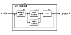
- FIG. 1 is a block diagram showing the configuration of the inverse matrix calculation device according to the first embodiment of the present invention.
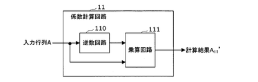
- FIG. 2 is a block diagram showing the configuration of the coefficient calculation circuit according to the first embodiment.
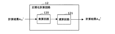
- FIG. 3 is a block diagram showing the configuration of the normalization calculation circuit according to the first embodiment.
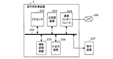
- FIG. 4 is a block diagram showing an example of a computer that realizes the inverse matrix calculation device according to the first embodiment.
- FIG. 5 is a diagram showing an example of a program executed by the inverse matrix calculation device according to the first embodiment.
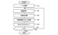
- FIG. 6 is a flow chart for explaining the operation of the inverse matrix calculation device according to the first embodiment.
- FIG. 7 is a diagram illustrating an example of a data structure stored in the memory according to the first embodiment.
- FIG. 8 is a block diagram showing the configuration of the inverse matrix calculation device according to the second embodiment.
- FIG. 9 is a block diagram showing the configuration of the normalization calculation circuit according to the third embodiment.
- FIG. 10 is a block diagram showing the configuration of the coefficient calculation circuit according to the fourth embodiment.
- FIG. 11 is a block diagram showing a configuration of an inverse matrix calculation device according to a conventional example.
- the inverse matrix calculation device receives the input matrix A as input, and calculates and outputs the inverse matrix A ⁇ 1 of the input matrix A based on the well-known Gaussian elimination method.
- the Gaussian elimination method is also called the sweeping method.
- the input matrix A is an Nth-order square matrix (N is an integer of 2 or more), and the output inverse matrix A ⁇ 1 is also an Nth-order square matrix.
- the input matrix A when the input matrix A is regular, the input matrix A has an inverse matrix A ⁇ 1 .
- I is a unit matrix with N rows and N columns
- the matrix whose product with the input matrix A is the unit matrix I is the inverse matrix A ⁇ 1 obtained by the inverse matrix calculation apparatus according to the present embodiment.
- the input matrix A and the two N-row N-column matrices of the staircase matrix modified so that the input matrix A becomes the unit matrix I are held in the storage area and the calculation processing of the inverse matrix A ⁇ 1 is performed.
- the inverse matrix calculation device performs the row basic transformation on the expanded matrix (A
- the inverse matrix calculation device 1 includes a coefficient calculation circuit 11, a normalization calculation circuit 12, and a memory 13.
- the coefficient calculation circuit 11 includes an inverse circuit 110 and a multiplication circuit (first multiplication circuit) 111.
- the reciprocal circuit 110 obtains and outputs the reciprocal of the value of the (i+1) row (i+1) column that is the diagonal element of the input matrix A.
- the reciprocal of the value of the diagonal component obtained by the reciprocal circuit 110 is stored in the memory 13 as the value of the (i+1) row (i+1) column of the unit matrix I in the expansion matrix (A
- the multiplication circuit 111 uses the reciprocal of the value of the (i+1)th row (i+1)th column which is the diagonal component of the input matrix A calculated by the reciprocal circuit 110, and uses the reciprocal of the value of the (i+1)th row of the expanded matrix (A
- the multiplication circuit 111 reads the first row component of the input matrix A stored in the memory 13 in advance, and the multiplication circuit 111 stores the first row component of the input matrix A in the first row of the expanded matrix (A
- the multiplication circuit 111 performs multiplication processing for each row by N rows to obtain a calculation result A 11 ′ of the coefficient calculation for each row.
- the calculation result A 11 ′ includes the multiplication result of each component for one row of the input matrix A and the reciprocal value obtained by the reciprocal circuit 110.
- the reciprocal number obtained by the reciprocal number circuit 110 can be used as a value obtained by multiplying the diagonal component of the unit matrix I by the reciprocal number.
- the normalization calculation circuit 12 uses the calculation result A 11 ′ by the coefficient calculation circuit 11 to normalize and calculate the (i+1)-th row (i+1)-column component of the expanded matrix (A
- the result A 12 '(second calculation result) is output.
- the normalization calculation circuit 12 includes a multiplication circuit (second multiplication circuit) 120 and a subtraction circuit 121.
- the multiplication circuit 120 multiplies the calculation result A 11 ′ obtained by the coefficient calculation circuit 11 by the value of the (i+1)th column component of each row of the input matrix A read from the memory 13.
- I) is added to the component in the first row and the first column of the input matrix A.
- the value obtained by multiplying the reciprocal of is obtained.
- the multiplication circuit 120 multiplies the calculation result A 11 ′ by the value of the second row, first column component of the input matrix A.
- the multiplication circuit 120 repeats the same calculation for the third row to the 32nd row (Nth row) of the expanded matrix (A
- the subtraction circuit 121 subtracts each component included in the row of the expanded matrix (A
- the subtraction circuit 121 determines that the 2nd row and 1st column component of the input matrix A obtained by the multiplication circuit 120 and the calculation result A 11 ′ in the 1st row of the expansion matrix (A
- the memory 13 is a readable/writable memory and stores an input matrix A of N rows and N columns input from the outside. More specifically, a storage area corresponding to the size of the input matrix A is secured in the memory 13, and it is possible to always store components of only N rows and N columns.
- the processor 102 which will be described later, performs one row of the expanded matrix (A
- the memory 13 stores an N-row N-column matrix having (i+2) column components as 1-row 1-column components. Further, the processor 102 performs a normalization calculation on the (i+2)-row (i+2)-column components of the expanded matrix (A
- the processor 102 stores the input matrix A in the memory 13 in advance, writes the calculation results A 11 ′ and A 12 ′ by the coefficient calculation circuit 11 and the normalization calculation circuit 12, and writes the input matrix A of the input matrix A. Update information.
- the processor 102 in the calculation result A 12 ′ by the normalization calculation circuit 12, the N rows after (i+2) after the column in which the input matrix A in the expansion matrix (A
- the components of N columns are stored in the memory 13 as a matrix A′ having significant values.
- the memory 13 stores desired N rows and N columns. That is, the inverse matrix A ⁇ 1 of A is stored.
- the processor 102 outputs the N-row N-column matrix stored in the memory 13 when the normalization calculation from the first row to the N-th row is completed, as the inverse matrix A ⁇ 1 of the input matrix A.
- the inverse matrix computing device 1 includes, for example, a computer including a processor 102, a main storage device 103, a communication interface 104, an auxiliary storage device 105, and an input/output device 106, which are connected via a bus 101. It can be realized by a program that controls these hardware resources.
- the display device 107 may be connected via the bus 101, and the calculation result and the like may be displayed on the display screen.
- the main storage device 103 is realized by, for example, a semiconductor memory such as SRAM, DRAM, and ROM.
- the main storage device 103 realizes the memory 13 described in FIG.
- the processor 102 controls the memory 13 described in FIG.
- a program for the processor 102 to perform various controls and calculations is stored in the main storage device 103 in advance.
- the processor 102 and the main storage device 103 realize each function of the inverse matrix calculation device 1 including the coefficient calculation circuit 11 and the normalization calculation circuit 12 shown in FIGS. 1 to 3.
- the communication interface 104 is an interface circuit for communicating with various external electronic devices via the communication network NW.
- the inverse matrix calculation device 1 may receive the input matrix A from the outside via the communication interface 104 or send the obtained inverse matrix A ⁇ 1 to the outside.
- the communication interface 104 for example, an operation interface and an antenna compatible with wireless data communication standards such as LTE, 3G, wireless LAN, and Bluetooth (registered trademark) are used.
- the communication network NW includes, for example, a WAN (Wide Area Network), a LAN (Local Area Network), the Internet, a dedicated line, a wireless base station, a provider, and the like.
- the auxiliary storage device 105 is composed of a readable/writable storage medium and a drive device for reading/writing various information such as programs and data from/to the storage medium.
- a semiconductor memory such as a hard disk or a flash memory can be used as a storage medium.
- the auxiliary storage device 105 has a program storage area for storing a program for the inverse matrix calculation device 1 to perform a calculation process for obtaining the inverse matrix A ⁇ 1 . Further, the auxiliary storage device 105 may have, for example, a backup area for backing up the above-mentioned data and programs.
- the auxiliary storage device 105 can store, for example, the inverse matrix calculation program shown in FIG.
- the input/output device 106 is configured by an I/O terminal that inputs a signal from an external device such as the display device 107 or outputs a signal to the external device.
- the inverse matrix calculation device 1 is not limited to being realized by one computer, but may be distributed by a plurality of computers connected to each other by the communication network NW.
- the processor 102 may be realized by hardware such as FPGA (Field-Programmable Gate Array), LSI (Large Scale Integration), and ASIC (Application Specific Circuit).
- the coefficient calculation circuit 11 calculates the coefficient for the first row of the input matrix A (step S2). More specifically, the reciprocal circuit 110 reads the input matrix A from the memory 13 and obtains the reciprocal of the 1st row and 1st column component. The obtained reciprocal number is input to the multiplication circuit 111 and is multiplied by each component of the first row of the input matrix A. For example, the multiplication circuit 111 performs multiplication N times in total.
- the coefficient calculation circuit 11 outputs the multiplication result of the first row of the input matrix A and the calculation result A 11 ′ having the reciprocal of the 1st row and 1st column component.
- the processor 102 reflects the multiplication result of the first row of the input matrix A included in the calculation result A 11 ′ on the first row of the memory 13 shown in the upper part of FIG. 7.
- the information regarding the reciprocal can be temporarily stored in another area of the memory 13.
- the normalization calculation circuit 12 calculates the (i+1)th row (i+1)th column component of the expanded matrix (A
- the subtraction circuit 121 outputs a calculation result A 12 ′ obtained by subtracting each component of the second row from the multiplication result of the first row by the multiplication circuit 120.
- the multiplication circuit 120 and the subtraction circuit 121 repeatedly perform the same processing from the third row to the 32nd row (Nth row) based on the calculation result A 11 ′ of the first row obtained in step S2, and input the same.
- I) is output.
- the processor 102 stores the matrix A′ of N rows and N columns included in the calculation result A 12 ′ output from the normalization calculation circuit 12 in the memory 13 (step S4). For example, as shown in the middle of FIG. 7, the processor 102 writes, in the memory 13, a matrix A′ made up of components of N rows and N columns having a significant value in the calculation result A 12 ′ by the normalization calculation circuit 12. , The N-row N-column matrix stored in the memory 13 is updated.
- the second row of the input matrix A is stored in the area corresponding to the first row as a row to be normalized in the next process (arrow b), and subsequently, the components of the third and subsequent rows are sequentially stored. It is stored (arrow c).
- the processor 102 increments i (step S5).
- step S6 NO
- the normalization calculation circuit 12 performs the normalization calculation for stepping the second column of the input matrix A based on the calculation result A 11 ′ by the coefficient calculation circuit 11 (step S3).
- the processor 102 in the calculation result A 12 ′ of the normalization calculation, has a matrix A′ including N rows and N columns of components including a significant value. Is stored in the memory 13 (step S4). More specifically, the processor 102 stores, in the memory 13, the components of the Nth row and the Nth column after the third column of the expanded matrix (A
- the matrix A′ of N rows and N columns stored in the memory 13 by the processor 102 is a matrix corresponding to the desired inverse matrix A ⁇ 1 .
- the coefficient calculation (step S2) and the normalization calculation (step S3) are repeated for N rows, so that the matrix A finally stored in the memory 13 is output as the inverse matrix A ⁇ 1 .
- the input matrix A of N rows and N columns is processed by the inverse matrix of N rows and N columns based on the Gaussian elimination method.
- the calculation process for outputting A ⁇ 1 only the matrix of N rows and N columns is stored in the memory 13. Therefore, in the conventional technique, in the memory, an area for holding the matrix data of two N rows and N columns corresponding to the input matrix A and the unit matrix I is required, whereas the memory amount is reduced and The circuit scale can be cut in half.
- the time required for memory access can be reduced, so that the calculation process including the coefficient calculation process and the normalization calculation can be sped up.
- FIG. 11 shows the configuration of an inverse matrix calculation device according to a conventional example described in Patent Document 1, for example.
- the inverse matrix A ⁇ 1 of the input matrix A of the N-th order square matrix is calculated by using N coefficient calculation sections and N normalization calculation sections. Seeking in parallel.
- the conventional inverse matrix computing device as described above targets a matrix having a relatively small size, and the circuit size is N times or more the matrix size N. Therefore, the inverse matrix calculation device for a matrix having a relatively large size may run out of resources even if an FPGA having a large logic scale is used.
- the inverse matrix calculation device 1 can handle a matrix having a relatively large size even when the calculation resources are limited.
- the inverse matrix calculation device 1 includes one normalization calculation circuit 12.
- the inverse matrix calculation device 1A according to the second embodiment includes a plurality of normalization calculation circuits 12a and 12b and performs normalization calculations in parallel. For example, in the sample code described in FIG. 5, the normalization calculation indicated by the dotted frame 5a is performed in parallel.
- the configuration different from that of the first embodiment will be mainly described.
- the inverse matrix calculation device 1A includes a coefficient calculation circuit 11, a plurality of normalization calculation circuits 12a and 12b, and a memory 13.
- the inverse matrix calculation device 1A receives an input matrix A of N rows and N columns and outputs an inverse matrix A ⁇ 1 of N rows and N columns based on the Gaussian elimination method.
- the inverse matrix calculation device 1A includes M (for example, M is an integer of 2 or more and N-1 or less) normalization calculation circuits 12a and 12b.
- the plurality of normalization calculation circuits 12a and 12b are connected in parallel.
- the inverse matrix calculation device 1A includes two normalization calculation circuits 12a and 12b.
- Each of the normalization calculation circuits 12a and 12b has a multiplication circuit 120 and a subtraction circuit 121, as shown in FIG.
- the normalization calculation circuits 12a and 12b normalize the (i+1)th row (i+1)th column component of the input matrix A using the calculation result A 11 ′ obtained by the coefficient calculation circuit 11.
- the processor 102 includes N rows after the column in which the input matrix A of the expanded matrix (A
- the matrix A′ for N columns is stored in the memory 13.
- the N-row N-column matrix stored in the memory 13 is updated.
- the inverse matrix calculation device 1A since the M normalization calculation circuits 12a and 12b perform the normalization calculations in parallel, the input matrix A of N rows and N columns is processed. Does not require normalization calculation for N rows. As a result, the inverse matrix calculation device 1A can speed up the calculation process for obtaining the inverse matrix A ⁇ 1 .
- the M number of the normalization calculation circuits 12a and 12b is set to an optimum number in consideration of, for example, the size of the input matrix A, the resources of the hardware such as the FPGA to be used, and the desired processing speed. do it.
- the normalization calculation circuit 12 includes one multiplication circuit 120 and one subtraction circuit 121 .
- the inverse matrix calculation device 1A includes the plurality of normalization calculation circuits 12a and 12b and performs the normalization calculation in parallel.
- the inverse matrix calculation device 1 according to the third embodiment includes a plurality of multiplication circuits 120a and 120b and subtraction circuits 121a and 121b in one normalization calculation circuit 12B.
- the inverse matrix calculation device 1 according to the third embodiment for example, in the sample code described with reference to FIG. 5, performs the internal process of the normalization calculation indicated by the dotted frame 5b in parallel.
- Other configurations of the inverse matrix calculation device 1 according to the third embodiment are the same as those of the first embodiment (FIGS. 1, 2, and 4).
- the normalization calculation circuit 12B receives the calculation result A 11 ′ by the coefficient calculation circuit 11 as input, performs normalization calculation including multiplication processing and subtraction processing of each component for each row, and outputs a calculation result A 12 ′. ..
- the input matrix A of N rows and N columns has N components per row, and requires N multiplications and subtractions.
- the normalization calculation circuit 12B processes, for example, the multiplication and subtraction required for the calculation per row in parallel.
- the normalization calculation circuit 12B performs the normalization calculation for N rows and outputs the calculation result A 12 ′.
- the processor 102 updates the matrix stored in the memory 13 with the matrix A′ of N rows and N columns including a significant value among the calculation results A 12 ′ based on the subtraction results output from the subtraction circuits 121a and 121b. To do.
- the normalization calculation circuit 12B processes multiplication and subtraction in parallel by the M multiplication circuits 120a and 120b and the subtraction circuits 121a and 121b, so that one row worth of data is processed. It is possible to reduce the number of repeated calculations in the normalization calculation process. Since the normalization calculation process for one row can be sped up, as a result, the calculation process for obtaining the inverse matrix A ⁇ 1 can be sped up.
- the normalization calculation circuit 12B according to the third embodiment described above can be combined with the M normalization calculation circuits 12a and 12b according to the second embodiment.
- the M numbers of the multiplication circuits 120a and 120b and the subtraction circuits 121a and 121b for example, in consideration of the size of the input matrix A, the resources of the hardware such as the FPGA to be used, and the desired processing speed, The optimum number should be set.
- the coefficient calculation circuit 11 includes the reciprocal circuit 110 and one multiplication circuit 111 has been described.
- the normalization calculation circuit 12B includes the plurality of multiplication circuits 120a and 120b and the subtraction circuits 121a and 121b and processes the normalization calculation for one row in parallel has been described.
- the coefficient calculation circuit 11A includes a plurality of multiplication circuits 111a and 111b.
- the inverse matrix calculation device 1 according to the fourth embodiment for example, in the sample code described with reference to FIG. 5, performs internal processing of coefficient calculation indicated by a dotted frame 5c in parallel.
- the rest of the configuration of the inverse matrix calculation device 1 according to the fourth embodiment is similar to that of the first embodiment (FIGS. 1, 3, and 4).
- the coefficient calculation circuit 11A includes an inverse circuit 110 and M (M is an integer of 2 or more and N or less) multiplication circuits 111a and 111b.
- M is an integer of 2 or more and N or less
- the reciprocal circuit 110 obtains the reciprocal of the value of the diagonal component (i+1) row (i+1) column component.
- each of the multiplier circuit 111a is written into the memory 13 the multiplication result and the reciprocal by 111b as the calculation result A 11 '.
- the coefficient calculation circuit 11A includes M number of multiplication circuits 111a and 111b, and performs the multiplication process in the coefficient calculation in parallel. It is possible to reduce the number of calculations and speed up the coefficient calculation process.
- the inverse matrix calculation device 1 including the coefficient calculation circuit 11A according to the fourth embodiment can further speed up the calculation process for obtaining the inverse matrix A ⁇ 1 .
- the optimum number is set in consideration of, for example, the size of the input matrix A, the resources of the hardware such as the FPGA to be used, and the desired processing speed. Good.
- the coefficient calculation circuit 11A according to the fourth embodiment can be combined with any of the second to third embodiments as appropriate.
- the inverse matrix calculation device deals with a matrix having a real number as a component, it can also handle a matrix having a complex number as a component.
- the inverse matrix calculation device is mounted in a scheduler of a wireless network system including a plurality of UEs and antennas adopting a coordinated wireless resource control method, and is dedicated to calculating system throughput and transmission weight matrix.
Landscapes
- Engineering & Computer Science (AREA)
- Physics & Mathematics (AREA)
- General Physics & Mathematics (AREA)
- Mathematical Physics (AREA)
- Pure & Applied Mathematics (AREA)
- Mathematical Analysis (AREA)
- Mathematical Optimization (AREA)
- Computational Mathematics (AREA)
- Data Mining & Analysis (AREA)
- Theoretical Computer Science (AREA)
- Computing Systems (AREA)
- Algebra (AREA)
- Databases & Information Systems (AREA)
- Software Systems (AREA)
- General Engineering & Computer Science (AREA)
- Complex Calculations (AREA)
Abstract
計算リソースに限りがある場合であっても、比較的大きいサイズの行列を扱うことができる逆行列計算装置を提供することを目的とする。 逆行列計算装置1は、N行N列の入力行列Aにおける拡大行列(A|I)に対してガウスの消去法に基づき行基本変形を行うプロセッサ102と、N行N列行列を記憶するメモリ13とを備え、プロセッサ102は、拡大行列の(i+1)行(i+1)列(i=0,1,・・・,N-1)成分の正規化計算を行う毎に、計算後の拡大行列のうち1行(i+2)列成分を1行1列成分とするN行N列行列をメモリ13に記憶させるとともに、メモリ13に記憶されたN行N列行列に基づいて、計算後の拡大行列の(i+2)行(i+2)列成分について正規化計算を繰り返し、第1行から第N行まで計算が終了したときにメモリ13が記憶するN行N列行列を逆行列A-1として出力する。
Description
本発明は、逆行列計算装置および逆行列計算処理方法に関する。
スマートフォンの普及に伴って、通信速度の向上や利用帯域の増大など、無線ネットワークに対する社会的な要請が大きくなっている。このような状況を背景として、LTE(Long Term Evolution)と呼ばれる移動通信方式の無線インターフェース仕様を適用した無線ネットワークシステムが普及しつつある。
このLTEでは、無線アクセス技術の1つとして、複数の送信ポイント(TP:基地局)が協調してユーザ端末(UE:ユーザ無線端末)と信号を送受信するCoMP(Coordinated Multi-point transmission/reception:セル間協調送受信)が採用されている(非特許文献1参照)。
CoMP技術は、周波数利用効率やセル端ユーザスループットを向上させる重要な技術の1つである。例えば、下り方向の通信(TPからUEへの送信)において、同時に複数の送信ポイントが同一周波数帯を用いて、各UEに送信することで無線リソースの利用効率を高めることができる。しかし、各送信ポイントが異なるUEに対して送信した場合、複数の送信ポイントから信号を受信可能なUEにとっては、他の送信ポイントからの信号が所望の受信信号の干渉となって、かえってスループットの低下を招く恐れがある。したがって、このような干渉を抑制しつつ通信速度を向上させるためにCoMPは必要不可欠な技術となっている。
さらに、LTEを発展させた次世代移動通信方式の研究開発が行われており、CoMPを拡張した概念として協調無線リソース制御方式、およびその処理を高速化するための専用回路構成が提案されている(非特許文献2参照)。協調無線リソース制御方式では、1ミリ秒からサブミリ秒程度の短時間の間に逆行列計算を数百回程度以上行う必要があり、その処理の高速化が必要不可欠である。
そこで、例えば、特許文献1には、n次正方行列(nは2以上の整数。)の逆行列をn並列で求める逆行列計算装置が開示されている。特許文献1に記載の逆行列計算装置は、比較的小さいサイズの行列をターゲットとしており、行列サイズnに対して回路規模がn倍以上になる。
田岡 他「LTE-AdvancedにおけるMIMOおよびセル間協調送受信技術」,NTT DOCOMO テクニカル・ジャーナル,Vol.18,No.2,pp.22-30,2010年7月,[online]<https://www.nttdocomo.co.jp/binary/pdf/corporate/technology/rd/technical_journal/bn/vol18_2/vol18_2_022jp.pdf>
Y.Arikawa,T.Sakamoto and S.Kimura,"Hardware accelerator for coordinated radio-resource scheduling in 5G ultra-high-density distributed antenna systems,"2017 27th International Telecommunication Networks and Applications Conference(ITNAC),Melbourne, pp. 1-6,November 2017.
特許文献1に記載の技術において、比較的大きいサイズの行列を扱う場合、回路規模が増大してしまい、ロジック規模の比較的大きいFPGAなどを用いたとしても、計算リソースの制限を受けるため、逆行列計算装置を実現することが困難となる。
本発明は、上述した課題を解決するためになされたものであり、計算リソースに限りがある場合であっても、比較的大きいサイズの行列を扱うことができる逆行列計算装置を提供することを目的とする。
上述した課題を解決するために、本発明に係る逆行列計算装置は、N次正方行列(Nは2以上の整数)の入力行列を入力とし、この入力行列の逆行列を出力する逆行列計算回路であって、前記入力行列にN次の単位行列を行方向に結合した拡大行列に対して、ガウスの消去法に基づき、行基本変形の処理を行うプロセッサと、N行N列行列を記憶する読み書き可能なメモリと、を備え、前記プロセッサは、前記拡大行列の(i+1)行(i+1)列(i=0,1,・・・,N-1)成分について正規化計算を行うごとに、正規化計算後の拡大行列のうち、1行(i+2)列成分を1行1列成分とするN行N列行列を前記メモリに記憶させるとともに、このメモリに記憶された前記N行N列行列に基づいて、前記正規化計算後の拡大行列の(i+2)行(i+2)列成分について正規化計算を行う処理を繰り返し、第1行から第N行まで正規化計算が終了したときの前記メモリに記憶されているN行N列行列を前記逆行列として出力することを特徴とする。
また、本発明に係る逆行列計算装置において、前記プロセッサは、前記入力行列の対角成分である(i+1)行(i+1)列(i=0,1,・・・,N-1)成分の値の逆数を前記拡大行列の(i+1)行目の各成分に乗算して第1計算結果を出力する係数計算回路と、前記第1計算結果を用いて、前記拡大行列の(i+1)行目の各成分を正規化して第2計算結果を出力する正規化計算回路と、を有し、前記プロセッサは、前記第2計算結果に含まれる1行(i+2)列目を1行1列成分とするN行N列の成分を前記メモリに書き込み、前記メモリに記憶されているN行N列行列を更新してもよい。
また、本発明に係る逆行列計算装置において、前記係数計算回路は、前記入力行列の対角成分である(i+1)行(i+1)列の値の逆数を求める逆数回路と、前記逆数を前記拡大行列の(i+1)行目の各成分に乗算する第1乗算回路と、を有し、前記係数計算回路は、前記拡大行列の行ごとに計算された前記第1計算結果を出力してもよい。
また、本発明に係る逆行列計算装置において、前記係数計算回路には、前記第1乗算回路が並列に計算可能に複数具備されていてもよい。
また、本発明に係る逆行列計算装置において、前記正規化計算回路は、前記第1計算結果に前記入力行列の行ごとの(i+1)列目の成分の値を乗算する第2乗算回路と、前記第2乗算回路による乗算結果から、前記第2乗算回路が計算の対象とした前記入力行列の行に対応する前記拡大行列の行に含まれる各成分を減算する減算回路と、を有し、前記正規化計算回路は、乗算および減算を繰り返し行ってN行分の前記第2計算結果を出力してもよい。
また、本発明に係る逆行列計算装置において、前記正規化計算回路には、前記第2乗算回路および前記減算回路が並列に計算可能に複数具備されていてもよい。
また、本発明に係る逆行列計算装置において、前記正規化計算回路は、並列に計算可能に複数具備されていてもよい。
上述した課題を解決するために、本発明に係る逆行列計算処理方法は、N次正方行列(Nは2以上の整数)の入力行列を入力とし、この入力行列の逆行列を出力する逆行列計算処理方法であって、前記入力行列にN次の単位行列を行方向に結合した拡大行列に対して、ガウスの消去法に基づき、行基本変形の処理を行うプロセッサが、前記拡大行列の(i+1)行(i+1)列(i=0,1,・・・,N-1)成分について正規化計算を行うごとに、正規化計算後の拡大行列のうち、1行(i+2)列成分を1行1列成分とするN行N列行列を読み書き可能なメモリに記憶させる第1ステップと、前記第1ステップで前記メモリに記憶された前記N行N列行列に基づいて、前記正規化計算後の拡大行列の(i+2)行(i+2)列成分について正規化計算を行う第2ステップと、前記第1ステップと前記第2ステップとを繰り返して、第1行から第N行までの正規化計算が終了したときの前記メモリに記憶されているN行N列行列を前記逆行列として出力する第3ステップとを備えることを特徴とする。
本発明によれば、行基本変形された拡大行列のうち、入力行列と同一のサイズの所定の行列成分をメモリに記憶するので、計算リソースに限りがある場合であっても、比較的大きいサイズの行列を扱うことができる。
以下、本発明の好適な実施の形態について、図1から図11を参照して詳細に説明する。
[発明の概要]
はじめに、本発明の実施の形態に係る逆行列計算装置の概要について説明する。逆行列計算装置は、入力行列Aを入力とし、よく知られたガウスの消去法に基づいて、入力行列Aの逆行列A-1を計算し出力する。ガウスの消去法は掃き出し法とも呼ばれる。本実施の形態では、入力行列AはN次正方行列(Nは2以上の整数)であり、また、出力される逆行列A-1もN次正方行列である。
[発明の概要]
はじめに、本発明の実施の形態に係る逆行列計算装置の概要について説明する。逆行列計算装置は、入力行列Aを入力とし、よく知られたガウスの消去法に基づいて、入力行列Aの逆行列A-1を計算し出力する。ガウスの消去法は掃き出し法とも呼ばれる。本実施の形態では、入力行列AはN次正方行列(Nは2以上の整数)であり、また、出力される逆行列A-1もN次正方行列である。
ここで、入力行列Aが正則であるとき、入力行列Aは逆行列A-1を持つ。IをN行N列の単位行列としたとき、入力行列Aとの積が単位行列Iとなる行列が、本実施の形態に係る逆行列計算装置が求める逆行列A-1である。
従来の技術では、入力行列A、および入力行列Aを単位行列Iにするように変形した階段行列の2つのN行N列の行列を記憶領域に保持して逆行列A-1の計算処理を実行していた。これに対し、本実施の形態に係る逆行列計算装置は、拡大行列(A|I)に対して入力行列Aを単位行列Iにするように行基本変形を行って、階段行列(最終的に逆行列A-1となる行列)を求める計算過程に応じて、拡大行列(A|I)に含まれる所定のN行N列分の成分のみを記憶領域に格納する。
[第1の実施の形態]
まず、本発明の第1の実施の形態に係る逆行列計算装置1の構成を説明する。逆行列計算装置1は、図1に示すように、係数計算回路11、正規化計算回路12、およびメモリ13を備える。
まず、本発明の第1の実施の形態に係る逆行列計算装置1の構成を説明する。逆行列計算装置1は、図1に示すように、係数計算回路11、正規化計算回路12、およびメモリ13を備える。
係数計算回路11は、入力行列Aの対角成分である(i+1)行(i+1)列(i=0,1,・・・,N-1)の値の逆数を求め、(i+1)行目の各成分に対して、求めた逆数を乗算し、その計算結果A11’(第1計算結果)を出力する。
係数計算回路11は、図2に示すように、逆数回路110と乗算回路(第1乗算回路)111とを備える。
逆数回路110は、入力行列Aの対角成分である(i+1)行(i+1)列の値の逆数を求めて出力する。逆数回路110が求めた対角成分の値の逆数は、拡大行列(A|I)における単位行列Iの(i+1)行(i+1)列の値としてメモリ13に記憶される。
逆数回路110は、入力行列Aの対角成分である(i+1)行(i+1)列の値の逆数を求めて出力する。逆数回路110が求めた対角成分の値の逆数は、拡大行列(A|I)における単位行列Iの(i+1)行(i+1)列の値としてメモリ13に記憶される。
乗算回路111は、逆数回路110が計算した入力行列Aの対角成分である(i+1)行(i+1)列の値の逆数を用いて、拡大行列(A|I)の(i+1)行目の各成分ごとの乗算を行い、計算結果A11’を出力する。より詳細には、乗算回路111は、メモリ13に予め記憶されている入力行列Aの(i+1)行の成分を読み出して、入力行列Aの(i+1)行目の各成分に逆数を乗算する。
例えば、i=0とすると、乗算回路111は、メモリ13に予め記憶されている入力行列Aの1行目の成分を読み出して、拡大行列(A|I)の1行目に入力行列Aの1行1列成分の逆数を乗算する計算を行う。N行N列の入力行列Aの場合、乗算回路111は、1行分の乗算を行うにあたり、N個の成分ごとに合計N回の乗算を行う。
また、乗算回路111は乗算処理を行ごとにN行分の乗算を行い、行ごとの係数計算の計算結果A11’を得る。例えば、計算結果A11’には、入力行列Aの1行分の各成分の乗算結果と、逆数回路110によって求められた逆数の値とが含まれる。逆数回路110によって求められた逆数は、単位行列Iの対角成分に逆数が乗算された値として用いることができる。
次に、正規化計算回路12について説明する。正規化計算回路12は、図3に示すように、係数計算回路11による計算結果A11’を用いて、拡大行列(A|I)の(i+1)行(i+1)列成分を正規化し、計算結果A12’(第2計算結果)を出力する。
正規化計算回路12は、乗算回路(第2乗算回路)120と減算回路121とを備える。
正規化計算回路12は、乗算回路(第2乗算回路)120と減算回路121とを備える。
乗算回路120は、係数計算回路11による計算結果A11’に、メモリ13から読み出した入力行列Aの行ごとの(i+1)列目の成分の値を乗算する。
例えば、i=0の場合において、係数計算回路11から出力された計算結果A11’として、拡大行列(A|I)の1行目の各成分に入力行列Aの1行1列目の成分の逆数を乗算した値が得られる。乗算回路120は、計算結果A11’に対して入力行列Aの2行1列目の成分の値を乗算する。乗算回路120は、拡大行列(A|I)の3行目から32行目(N行目)についても同様の計算を繰り返して行う。このように、1行1列成分の正規化を行うときに、乗算回路120は、合計N-1回(N-1行分)の乗算を行う。
減算回路121は、乗算回路120による乗算結果から、乗算回路120が計算の対象とした入力行列Aの行に対応する拡大行列(A|I)の行に含まれる各成分を減算して計算結果A12’を出力する。
具体的には、i=0の場合、減算回路121は、乗算回路120が求めた入力行列Aの2行1列成分と拡大行列(A|I)の1行目における計算結果A11’との乗算結果から、拡大行列(A|I)の2行目の各成分を減算する。減算回路121は、同様の計算を拡大行列(A|I)の3行目から32行目(N行目)まで行う。
このように、i=0の場合に、減算回路121が2行目から32行目までの減算処理を行うと、拡大行列(A|I)において、入力行列Aの1列目が階段化されることになる。減算回路121によってN-1回(N-1行分)の減算処理が繰り返し行われる結果、階段化された列を含む拡大行列(A|I)が計算結果A12’として得られる。
メモリ13は、読み書き可能なメモリであり、外部から入力されるN行N列の入力行列Aを記憶する。より詳細には、メモリ13には、入力行列Aのサイズに応じた記憶領域が確保されており、常にN行N列分だけの成分を記憶することができる。
後述するプロセッサ102は、拡大行列(A|I)の(i+1)行(i+1)列成分について正規化計算が行われるごとに、正規化計算後の拡大行列(A|I)のうち、1行(i+2)列成分を1行1列成分とするN行N列行列をメモリ13に記憶させる。さらに、プロセッサ102は、メモリ13に記憶されたN行N列行列に基づいて、正規化計算後の拡大行列(A|I)の(i+2)行(i+2)列成分について正規化計算を行う処理を繰り返す。
より詳細には、プロセッサ102は、メモリ13に予め入力行列Aを記憶させ、係数計算回路11および正規化計算回路12による計算結果A11’、A12’を書き込んでいって、入力行列Aの情報を更新する。
具体的には、プロセッサ102は、正規化計算回路12による計算結果A12’のうち、拡大行列(A|I)における入力行列Aが階段化された列より後の(i+2)以降のN行N列分の成分について、有意な値を有する行列A’として、メモリ13に記憶させる。
係数計算回路11および正規化計算回路12による上述した繰り返し計算が全て完了したとき、すなわち拡大行列(A|I)に対する行基本変形が完了したときに、メモリ13には、所望のN行N列の逆行列A-1が記憶されていることになる。
プロセッサ102は、1行目からN行目までの正規化計算が終了したときにメモリ13が記憶しているN行N列行列を、入力行列Aの逆行列A-1として出力する。
[逆行列計算装置のコンピュータ構成]
次に、上述した構成を有する逆行列計算装置1を実現するコンピュータ構成の一例について図4を参照して説明する。
図4に示すように、逆行列計算装置1は、例えば、バス101を介して接続されるプロセッサ102、主記憶装置103、通信インターフェース104、補助記憶装置105、入出力装置106を備えるコンピュータと、これらのハードウェア資源を制御するプログラムによって実現することができる。逆行列計算装置1は、例えば、表示装置107がバス101を介して接続され、表示画面に計算結果などを表示してもよい。
次に、上述した構成を有する逆行列計算装置1を実現するコンピュータ構成の一例について図4を参照して説明する。
図4に示すように、逆行列計算装置1は、例えば、バス101を介して接続されるプロセッサ102、主記憶装置103、通信インターフェース104、補助記憶装置105、入出力装置106を備えるコンピュータと、これらのハードウェア資源を制御するプログラムによって実現することができる。逆行列計算装置1は、例えば、表示装置107がバス101を介して接続され、表示画面に計算結果などを表示してもよい。
主記憶装置103は、例えば、SRAM、DRAM、およびROMなどの半導体メモリによって実現される。主記憶装置103は、図1で説明したメモリ13を実現する。
プロセッサ102は、図1で説明したメモリ13の制御を行う。
プロセッサ102は、図1で説明したメモリ13の制御を行う。
主記憶装置103には、プロセッサ102が各種制御や演算を行うためのプログラムが予め格納されている。プロセッサ102と主記憶装置103とによって、図1から図3に示した係数計算回路11や正規化計算回路12を含む逆行列計算装置1の各機能が実現される。
通信インターフェース104は、通信ネットワークNWを介して各種外部電子機器との通信を行うためのインターフェース回路である。逆行列計算装置1は、通信インターフェース104を介して外部から入力行列Aを受信したり、求めた逆行列A-1を外部に送出してもよい。
通信インターフェース104としては、例えば、LTE、3G、無線LAN、Bluetooth(登録商標)などの無線データ通信規格に対応した演算インターフェースおよびアンテナが用いられる。通信ネットワークNWは、例えば、WAN(Wide Area Network)やLAN(Local Area Network)、インターネット、専用回線、無線基地局、プロバイダなどを含む。
補助記憶装置105は、読み書き可能な記憶媒体と、その記憶媒体に対してプログラムやデータなどの各種情報を読み書きするための駆動装置とで構成されている。補助記憶装置105には、記憶媒体としてハードディスクやフラッシュメモリなどの半導体メモリを使用することができる。
補助記憶装置105は、逆行列計算装置1が逆行列A-1を求める計算処理を行うためのプログラムを格納するプログラム格納領域を有する。さらには、補助記憶装置105は、例えば、上述したデータやプログラムやなどをバックアップするためのバックアップ領域などを有していてもよい。補助記憶装置105は、例えば、図5に示す逆行列計算プログラムを記憶することができる。
入出力装置106は、表示装置107など外部機器からの信号を入力したり、外部機器へ信号を出力したりするI/O端子により構成される。
なお、逆行列計算装置1は、1つのコンピュータによって実現される場合だけでなく、互いに通信ネットワークNWで接続された複数のコンピュータによって分散されていてもよい。また、プロセッサ102は、FPGA(Field-Programmable Gate Array)、LSI(Large Scale Integration)、ASIC(Application Specific Integrated Circuit)等のハードウェアによって実現されていてもよい。
[逆行列計算装置の動作]
次に、上述した構成を有する逆行列計算装置1の動作について、図6および図7を参照して説明する。N行N列の入力行列Aは、外部から逆行列計算装置1に入力され、予めメモリ13に記憶されているものとする。例えば、メモリ13は、図7の上段に示すように、入力行列Aの各成分を記憶している。
次に、上述した構成を有する逆行列計算装置1の動作について、図6および図7を参照して説明する。N行N列の入力行列Aは、外部から逆行列計算装置1に入力され、予めメモリ13に記憶されているものとする。例えば、メモリ13は、図7の上段に示すように、入力行列Aの各成分を記憶している。
まず、プロセッサ102は、メモリ13に記憶されているN行N列の入力行列Aにおいて、i=0と設定して(i+1)行目を計算の対象として選択する(ステップS1)。より詳細には、プロセッサ102はi=0、すなわち入力行列Aの1行目を計算の対象として選択して処理を開始する。このとき、プロセッサ102は、拡大行列(A|I)を生成する。
次に、係数計算回路11は、入力行列Aの1行目についての係数計算を行う(ステップS2)。より詳細には、逆数回路110が、メモリ13から入力行列Aを読み出し、1行1列成分の逆数を求める。求められた逆数は、乗算回路111に入力され、入力行列Aの1行目の各成分と乗算される。例えば、乗算回路111は、合計N回の乗算を行う。
係数計算回路11は、入力行列Aの1行目の乗算結果と1行1列成分の逆数を有する計算結果A11’を出力する。プロセッサ102は、計算結果A11’に含まれる入力行列Aの1行目の乗算結果を、図7の上段に示すメモリ13の1行目に反映させる。なお、逆数に関する情報は、メモリ13の別領域に一時的に保持することができる。
その後、正規化計算回路12は、係数計算回路11によって求められた計算結果A11’に基づいて、拡大行列(A|I)の(i+1)行(i+1)列成分、すなわち1行1列成分の正規化を行う(ステップS3)。具体的には、乗算回路120は、ステップS2で係数計算処理された入力行列Aの1行目の各成分(計算結果A11’)をメモリ13から読み出して、入力行列Aの2行1列成分の値を乗算する。
その後、減算回路121は、乗算回路120による1行目に対する乗算結果から2行目の各成分を減算した計算結果A12’を出力する。乗算回路120および減算回路121は、同様の処理を、ステップS2で得られた1行目の計算結果A11’に基づいて、3行目から32行目(N行)まで繰り返して行い、入力行列Aの1列目が階段化された拡大行列(A|I)である計算結果A12’を出力する。
プロセッサ102は、正規化計算回路12から出力された計算結果A12’に含まれるN行N列の行列A’をメモリ13に格納する(ステップS4)。例えば、図7の中段に示すように、プロセッサ102は、正規化計算回路12による計算結果A12’のうち、有意な値を有するN行N列の成分からなる行列A’をメモリ13に書き込み、メモリ13に記憶されているN行N列行列を更新する。
なお、図7の中段に示すように、メモリ13が格納する行列A’の例では、入力行列Aの1行2列目から32列目および単位行列Iの1行1列成分の計算結果A11’からなる合計32個(=N個)の成分は、矢印aで示すように、メモリ13におけるN行目に相当する領域に格納されている。また、入力行列Aの2行目は、次の処理で正規化される行として第1行目に相当する領域に格納され(矢印b)、これに続いて3行目以降の成分が順番に格納される(矢印c)。
以上の手順により、入力行列Aの1列目が階段化され、i=0、すなわち入力行列Aの1行目の成分に基づいた係数計算および正規化計算が完了する。
次に、プロセッサ102は、iをインクリメントさせる(ステップS5)。上記の例では、プロセッサ102は、i=1にインクリメントして、入力行列Aの(i+1)行目、すなわち2行目を計算の対象として選択する。
その後、i=N-1となるまで(ステップS6:NO)、ステップS2からステップS5までの処理が繰り返し実行される。上記の例では、係数計算回路11は、メモリ13からi=1、すなわち入力行列Aの2行目に相当するデータを読み出して、係数計算を行う(ステップS2)。その後、正規化計算回路12は、係数計算回路11による計算結果A11’に基づいて、入力行列Aの第2列目を階段化するために正規化計算を行う(ステップS3)。
その後、プロセッサ102は、入力行列Aの第2列目の階段化が完了すると、正規化計算の計算結果A12’のうち、有意な値を含むN行N列分の成分からなる行列A’をメモリ13に記憶させる(ステップS4)。より詳細には、プロセッサ102は、行基本変形されている拡大行列(A|I)の3列目以降のN行N列の成分を行列A’としてメモリ13に格納する。
その後、i=N-1までの計算が行われると(ステップS6:YES)、処理は終了する。図7の下段に示すように。例えば、i=31にインクリメントされた場合に、プロセッサ102がメモリ13に格納するN行N列分の行列A’は、所望とされる逆行列A-1に相当する行列となる。このように、係数計算(ステップS2)および正規化計算(ステップS3)がN行分繰り返されることで、最終的にメモリ13に記憶されている行列Aが逆行列A-1として出力される。
以上説明したように、第1の実施の形態に係る逆行列計算装置1によれば、N行N列の入力行列Aに対して、ガウスの消去法に基づいて、N行N列の逆行列A-1を出力する計算処理において、N行N列分の行列のみをメモリ13に記憶する。そのため、従来の技術では、メモリにおいて、入力行列Aと単位行列Iに相当する2つのN行N列の行列データを保持する領域が必要であったのに対して、メモリ量が削減され、その回路規模を半分に抑えることができる。
また、第1の実施の形態に係る逆行列計算装置1によれば、メモリアクセスに要する時間が削減できるため、係数計算処理および正規化計算を含む計算処理をより高速化することができる。
ここで、本実施の形態に係る逆行列計算装置1との比較例として、図11に、例えば特許文献1に記載されている従来例に係る逆行列計算装置の構成を示す。図11に示す従来例に係る逆行列計算装置では、N次正方行列の入力行列Aの逆行列A-1をN個の係数計算部と、N個の正規化計算部とを用いて、N並列で求めている。
このような従来例の逆行列計算装置は、比較的小さいサイズの行列をターゲットとしており、行列サイズNに対して、回路規模がN倍以上となる。そのため、比較的大きいサイズの行列を対象とした逆行列計算装置は、ロジック規模が大きいFPGAを用いたとしても、リソースが不足してしまう場合がある。
これに対して、本実施の形態に係る逆行列計算装置1は、回路規模が削減されるので、計算リソースに限りがある場合であっても、比較的大きいサイズの行列を扱うことができる。
[第2の実施の形態]
次に、本発明の第2の実施の形態について説明する。なお、以下の説明では、上述した第1の実施の形態と同じ構成については同一の符号を付し、その説明を省略する。
次に、本発明の第2の実施の形態について説明する。なお、以下の説明では、上述した第1の実施の形態と同じ構成については同一の符号を付し、その説明を省略する。
第1の実施の形態では、逆行列計算装置1は1つの正規化計算回路12を備える場合について説明した。これに対し、第2の実施の形態に係る逆行列計算装置1Aは、複数の正規化計算回路12a、12bを備え、正規化計算を並列に行う。例えば、図5で説明したサンプルコードにおいて、点線の枠5aに示す正規化計算を並列に行う。以下、第1の実施の形態と異なる構成を中心に説明する。
図8に示すように、逆行列計算装置1Aは、係数計算回路11、複数の正規化計算回路12a、12b、およびメモリ13を備える。逆行列計算装置1Aは、N行N列の入力行列Aを入力として、ガウスの消去法に基づいて、N行N列の逆行列A-1を出力する。
逆行列計算装置1Aは、M個(例えば、Mは2以上かつN-1以下の整数)の正規化計算回路12a、12bを具備する。複数の正規化計算回路12a、12bは、並列に接続されている。図8の例では、逆行列計算装置1Aは、2つの正規化計算回路12a、12bを備えている。正規化計算回路12a、12bのそれぞれは、図3で示したように、乗算回路120と減算回路121とを有する。
正規化計算回路12a、12bは、係数計算回路11による計算結果A11’を用いて、入力行列Aの(i+1)行(i+1)列成分を正規化する。本実施の形態では、M個の正規化計算回路12a、12bでN行分の正規化計算を並列に処理する。したがって、例えば、図8の例に示すように、M=2の場合、各正規化計算回路12a、12bは、(N-1)/2行分の正規化計算を繰り返すことで、N行N列の入力行列Aにおける正規化計算を完了することができる。M=N-1の場合には、正規化計算は1回で完了することになる。特にNが3以上の場合に有効である。
プロセッサ102は、正規化計算回路12a、12bのそれぞれから出力されて得られた計算結果A12’に含まれる、拡大行列(A|I)の入力行列Aが階段化された列以降のN行N列分の行列A’をメモリ13に記憶させる。これによって、メモリ13記憶されていたN行N列行列が更新される。
このように、第2の実施の形態に係る逆行列計算装置1Aは、M個の正規化計算回路12a、12bが並列に正規化計算を行うので、N行N列の入力行列Aに対しては、N行分の正規化計算が不要となる。その結果として、逆行列計算装置1Aでは、逆行列A-1を求める計算処理を高速化することができる。
なお、正規化計算回路12a、12bのM個の数については、例えば、入力行列Aのサイズ、使用するFPGAなどのハードウェアのリソースや所望とされる処理速度などに鑑み、最適な個数を設定すればよい。
[第3の実施の形態]
次に、本発明の第3の実施の形態について説明する。なお、以下の説明では、上述した第1および第2の実施の形態と同じ構成については同一の符号を付し、その説明を省略する。
次に、本発明の第3の実施の形態について説明する。なお、以下の説明では、上述した第1および第2の実施の形態と同じ構成については同一の符号を付し、その説明を省略する。
第1の実施の形態では、正規化計算回路12は、1つの乗算回路120と1つの減算回路121を備える場合について説明した。また、第2の実施の形態では、逆行列計算装置1Aは、複数の正規化計算回路12a、12bを備え、並列に正規化計算を行う場合について説明した。
これに対して、第3の実施の形態に係る逆行列計算装置1は、複数の乗算回路120a、120bと、減算回路121a、121bとが1つの正規化計算回路12Bに具備されている。第3の実施の形態に係る逆行列計算装置1は、例えば、図5で説明したサンプルコードにおいて、点線の枠5bに示す正規化計算の内部処理を並列に行う。第3の実施の形態に係る逆行列計算装置1が備えるその他の構成は、第1の実施の形態と同様である(図1、図2、図4)。
正規化計算回路12Bは、係数計算回路11による計算結果A11’を入力とし、1行ごとの各成分の乗算処理と減算処理とからなる正規化計算を行い、計算結果A12’を出力する。例えば、N行N列の入力行列Aにおいては、1行あたりN個の成分を有し、N回の乗算および減算処理が必要となる。正規化計算回路12Bは、例えば、1行あたりの計算に必要とされる乗算および減算を並列に処理する。
図9に示すように、正規化計算回路12Bは、M個(Mは2以上かつN以下の整数)の乗算回路120a、120bと減算回路121a、121bとを備え、1行分の正規化計算をM並列で行う。そのため、N/M回の計算を繰り返すことで、1行分の正規化計算の結果を得ることができる。例えば、図9に示すように、M=2の場合、N/2回の乗算処理および減算処理を繰り返すことで、1行分の正規化計算の処理を完了することができる。M=Nの場合、1回の乗算および減算処理によって1行分の正規化計算を完了する。
正規化計算回路12Bは、N行分の正規化計算を行い、計算結果A12’を出力する。
プロセッサ102はそれぞれの減算回路121a、121bから出力される減算結果に基づく計算結果A12’のうち、有意な値を含むN行N列の行列A’でメモリ13に記憶されている行列を更新する。
プロセッサ102はそれぞれの減算回路121a、121bから出力される減算結果に基づく計算結果A12’のうち、有意な値を含むN行N列の行列A’でメモリ13に記憶されている行列を更新する。
このように、第3の実施の形態によれば、正規化計算回路12Bは、M個の乗算回路120a、120bおよび減算回路121a、121bにより乗算および減算を並列に処理するので、1行分の正規化計算処理における繰り返しの計算回数を削減することができる。1行分の正規化計算処理をより高速化できるため、結果として、逆行列A-1を求めるための計算処理を高速化することができる。
なお、説明した第3の実施の形態に係る正規化計算回路12Bは、第2の実施の形態に係るM個の正規化計算回路12a、12bと組み合わせることも可能である。このとき、乗算回路120a、120bおよび減算回路121a、121bのM個の数については、例えば、入力行列Aのサイズ、使用するFPGAなどのハードウェアのリソースや所望とされる処理速度などに鑑み、最適な個数を設定すればよい。
[第4の実施の形態]
次に、本発明の第4の実施の形態について説明する。なお、以下の説明では、上述した第1から第3の実施の形態と同じ構成については同一の符号を付し、その説明を省略する。
次に、本発明の第4の実施の形態について説明する。なお、以下の説明では、上述した第1から第3の実施の形態と同じ構成については同一の符号を付し、その説明を省略する。
第1の実施の形態では、係数計算回路11が逆数回路110と1つの乗算回路111とを備える場合について説明した。また、第3の実施の形態では、正規化計算回路12Bが複数の乗算回路120a、120bおよび減算回路121a、121bを備え、1行分の正規化計算を並列に処理する場合について説明した。
これに対し、第4の実施の形態では、係数計算回路11Aが複数の乗算回路111a、111bを備える。第4の実施の形態に係る逆行列計算装置1は、例えば、図5で説明したサンプルコードにおいて、点線の枠5cに示す係数計算の内部処理を並列に行う。なお、第4の実施の形態に係る逆行列計算装置1のその他の構成は第1の実施の形態と同様である(図1、図3、図4)。
図10に示すように、係数計算回路11Aは、逆数回路110とM個(Mは2以上かつN以下の整数)の乗算回路111a、111bを備える。
逆数回路110は、例えば、N行N列の入力行列Aが入力された場合に、対角成分である(i+1)行(i+1)列成分の値の逆数を求める。
逆数回路110は、例えば、N行N列の入力行列Aが入力された場合に、対角成分である(i+1)行(i+1)列成分の値の逆数を求める。
乗算回路111a、111bは、(i+1)行目の各成分に対して逆数回路110が求めた対角成分の逆数を乗算する。より詳細には、M個の乗算回路111a、111bのそれぞれは、入力行列Aの(i+1)行に含まれるN個の成分に対して行う乗算処理を並列に実行する。例えば、図10に示すように、M=2の場合、各乗算回路111a、111bのそれぞれは、N/2回の乗算処理を行う。このように、N回の繰り返しが必要な1行分の乗算処理について、本実施の形態に係るM個の乗算回路111a、111bを用いることで、係数計算をM並列で行う。
プロセッサ102は、それぞれの乗算回路111a、111bによる乗算結果および逆数を計算結果A11’としてメモリ13に書き込む。
このように、第4の実施の形態によれば、係数計算回路11AがM個の乗算回路111a、111bを備え、係数計算における乗算処理を並列に処理するので、1行分の各成分に対する係数計算の回数を削減して、係数計算処理をより高速化することができる。
また、第4の実施の形態に係る係数計算回路11Aを備えた逆行列計算装置1は、逆行列A-1を求める計算処理をより高速化することができる。
なお、乗算回路111a、111bのM個の数については、例えば、入力行列Aのサイズ、使用するFPGAなどのハードウェアのリソースや所望とされる処理速度などに鑑み、最適な個数を設定すればよい。
また、第4の実施の形態に係る係数計算回路11Aは、第2から第3の実施の形態と適宜組み合わせることも可能である。
以上、本発明の逆行列計算装置、および逆行列計算処理方法における実施の形態について説明したが、本発明は説明した実施の形態に限定されるものではなく、請求項に記載した発明の範囲において当業者が想定し得る各種の変形を行うことが可能である。
例えば、説明した実施の形態に係る逆行列計算装置は、実数を成分とする行列を扱う場合について説明したが、複素数を成分とする行列を扱うこともできる。
また、説明した実施の形態に係る逆行列計算装置は、協調無線リソース制御方式を採用した複数のUEおよびアンテナを含む無線ネットワークシステムのスケジューラに搭載され、システムのスループットや送信重み行列を計算する専用のアクセラレータとして用いることができる(非特許文献2参照)。本実施の形態に係る逆行列計算回路を用いることで、協調無線リソース制御方式の処理を高速化することができる。
1…逆行列計算装置、11…係数計算回路、12…正規化計算回路、13…メモリ、101…バス、102…プロセッサ、103…主記憶装置、104…通信インターフェース、105…補助記憶装置、106…入出力装置、107…表示装置、110…逆数回路、111、120…乗算回路、121…減算回路、NW…通信ネットワーク。
Claims (8)
- N次正方行列(Nは2以上の整数)の入力行列を入力とし、この入力行列の逆行列を出力する逆行列計算回路であって、
前記入力行列にN次の単位行列を行方向に結合した拡大行列に対して、ガウスの消去法に基づき、行基本変形の処理を行うプロセッサと、
N行N列行列を記憶する読み書き可能なメモリと、
を備え、
前記プロセッサは、前記拡大行列の(i+1)行(i+1)列(i=0,1,・・・,N-1)成分について正規化計算を行うごとに、正規化計算後の拡大行列のうち、1行(i+2)列成分を1行1列成分とするN行N列行列を前記メモリに記憶させるとともに、このメモリに記憶された前記N行N列行列に基づいて、前記正規化計算後の拡大行列の(i+2)行(i+2)列成分について正規化計算を行う処理を繰り返し、第1行から第N行まで正規化計算が終了したときの前記メモリに記憶されているN行N列行列を前記逆行列として出力する
ことを特徴とする逆行列計算装置。 - 請求項1に記載の逆行列計算装置において、
前記プロセッサは、
前記入力行列の対角成分である(i+1)行(i+1)列(i=0,1,・・・,N-1)成分の値の逆数を前記拡大行列の(i+1)行目の各成分に乗算して第1計算結果を出力する係数計算回路と、
前記第1計算結果を用いて、前記拡大行列の(i+1)行目の各成分を正規化して第2計算結果を出力する正規化計算回路と、
を有し、
前記プロセッサは、
前記第2計算結果に含まれる1行(i+2)列目を1行1列成分とするN行N列の成分を前記メモリに書き込み、前記メモリに記憶されているN行N列行列を更新する
ことを特徴とする逆行列計算装置。 - 請求項2に記載の逆行列計算装置において、
前記係数計算回路は、
前記入力行列の対角成分である(i+1)行(i+1)列の値の逆数を求める逆数回路と、
前記逆数を前記拡大行列の(i+1)行目の各成分に乗算する第1乗算回路と、
を有し、
前記係数計算回路は、
前記拡大行列の行ごとに計算された前記第1計算結果を出力する
ことを特徴とする逆行列計算装置。 - 請求項3に記載の逆行列計算装置において、
前記係数計算回路には、前記第1乗算回路が並列に計算可能に複数具備されていることを特徴とする逆行列計算装置。 - 請求項2から4のいずれか1項に記載の逆行列計算装置において、
前記正規化計算回路は、
前記第1計算結果に前記入力行列の行ごとの(i+1)列目の成分の値を乗算する第2乗算回路と、
前記第2乗算回路による乗算結果から、前記第2乗算回路が計算の対象とした前記入力行列の行に対応する前記拡大行列の行に含まれる各成分を減算する減算回路と、
を有し、
前記正規化計算回路は、
乗算および減算を繰り返し行ってN行分の前記第2計算結果を出力する
ことを特徴とする逆行列計算装置。 - 請求項5に記載の逆行列計算装置において、
前記正規化計算回路には、前記第2乗算回路および前記減算回路が並列に計算可能に複数具備されていることを特徴とする逆行列計算装置。 - 請求項2から6のいずれか1項に記載の逆行列計算装置において、
前記正規化計算回路は、並列に計算可能に複数具備されていることを特徴とする逆行列計算装置。 - N次正方行列(Nは2以上の整数)の入力行列を入力とし、この入力行列の逆行列を出力する逆行列計算処理方法であって、
前記入力行列にN次の単位行列を行方向に結合した拡大行列に対して、ガウスの消去法に基づき、行基本変形の処理を行うプロセッサが、
前記拡大行列の(i+1)行(i+1)列(i=0,1,・・・,N-1)成分について正規化計算を行うごとに、正規化計算後の拡大行列のうち、1行(i+2)列成分を1行1列成分とするN行N列行列を読み書き可能なメモリに記憶させる第1ステップと、
前記第1ステップで前記メモリに記憶された前記N行N列行列に基づいて、前記正規化計算後の拡大行列の(i+2)行(i+2)列成分について正規化計算を行う第2ステップと、
前記第1ステップと前記第2ステップとを繰り返して、第1行から第N行までの正規化計算が終了したときの前記メモリに記憶されているN行N列行列を前記逆行列として出力する第3ステップと
を備えることを特徴とする逆行列計算処理方法。
Priority Applications (1)
| Application Number | Priority Date | Filing Date | Title |
|---|---|---|---|
| US17/296,716 US20220004596A1 (en) | 2018-12-06 | 2019-11-22 | Inverse Matrix Calculation Device and Inverse Matrix Calculation Processing Method |
Applications Claiming Priority (2)
| Application Number | Priority Date | Filing Date | Title |
|---|---|---|---|
| JP2018-228878 | 2018-12-06 | ||
| JP2018228878A JP2020091691A (ja) | 2018-12-06 | 2018-12-06 | 逆行列計算装置および逆行列計算処理方法 |
Publications (1)
| Publication Number | Publication Date |
|---|---|
| WO2020116202A1 true WO2020116202A1 (ja) | 2020-06-11 |
Family
ID=70975449
Family Applications (1)
| Application Number | Title | Priority Date | Filing Date |
|---|---|---|---|
| PCT/JP2019/045782 Ceased WO2020116202A1 (ja) | 2018-12-06 | 2019-11-22 | 逆行列計算装置および逆行列計算処理方法 |
Country Status (3)
| Country | Link |
|---|---|
| US (1) | US20220004596A1 (ja) |
| JP (1) | JP2020091691A (ja) |
| WO (1) | WO2020116202A1 (ja) |
Families Citing this family (2)
| Publication number | Priority date | Publication date | Assignee | Title |
|---|---|---|---|---|
| JP7786124B2 (ja) * | 2021-10-26 | 2025-12-16 | 日本電気株式会社 | スクリプト実行方法 |
| CN114201731B (zh) * | 2022-02-18 | 2022-05-13 | 长沙金维信息技术有限公司 | 用于导航芯片的矩阵求逆方法 |
Citations (1)
| Publication number | Priority date | Publication date | Assignee | Title |
|---|---|---|---|---|
| JP2004533035A (ja) * | 2001-02-24 | 2004-10-28 | インターナショナル・ビジネス・マシーンズ・コーポレーション | クラス・ネットワーク経路指定 |
Family Cites Families (1)
| Publication number | Priority date | Publication date | Assignee | Title |
|---|---|---|---|---|
| CN106021188B (zh) * | 2016-05-11 | 2019-04-12 | 广州广电运通金融电子股份有限公司 | 浮点矩阵求逆的并行硬件架构和并行计算方法 |
-
2018
- 2018-12-06 JP JP2018228878A patent/JP2020091691A/ja active Pending
-
2019
- 2019-11-22 WO PCT/JP2019/045782 patent/WO2020116202A1/ja not_active Ceased
- 2019-11-22 US US17/296,716 patent/US20220004596A1/en not_active Abandoned
Patent Citations (1)
| Publication number | Priority date | Publication date | Assignee | Title |
|---|---|---|---|---|
| JP2004533035A (ja) * | 2001-02-24 | 2004-10-28 | インターナショナル・ビジネス・マシーンズ・コーポレーション | クラス・ネットワーク経路指定 |
Non-Patent Citations (3)
| Title |
|---|
| COMPREHENSIVE COMPUTER NUMERICAL CALCULATION: "ARUGA, MASAHIRO et al.", March 1996, ISBN: 4-274-13053-3, pages: 119 - 127 * |
| SHIMAUCHI, TAKAKAZU ET AL.: "Algorithm dictionary", 1998, ISBN: 4-320-02709-4, pages: 94 * |
| YUTO, ET AL.: "FPGA Implementation of Mahalanobis Distance-Based Outlier Detection for Streaming Data", IEICE TECHNICAL REPORT, vol. 116, no. 416, 2017, pages 141 - 146, ISSN: 0913-5685 * |
Also Published As
| Publication number | Publication date |
|---|---|
| JP2020091691A (ja) | 2020-06-11 |
| US20220004596A1 (en) | 2022-01-06 |
Similar Documents
| Publication | Publication Date | Title |
|---|---|---|
| WO2020145146A1 (ja) | 推論処理装置および推論処理方法 | |
| EP4072087B1 (en) | Data processing apparatus and method, base station, and storage medium | |
| CN110826685A (zh) | 神经网络卷积计算的方法和装置 | |
| CN114024587B (zh) | 基于全连接层共用的反馈网络编码器、架构及训练方法 | |
| WO2020116202A1 (ja) | 逆行列計算装置および逆行列計算処理方法 | |
| CN114830607A (zh) | 用于大型多维无线系统的无线x2x接入方法和接收器 | |
| US7856465B2 (en) | Combined fast fourier transforms and matrix operations | |
| CN115967593A (zh) | 导频信号发送方法、信道估计方法、装置及设备 | |
| WO2022012362A1 (zh) | 功率控制方法、装置、通信节点及存储介质 | |
| CN111356151B (zh) | 一种数据处理方法及装置、计算机可读存储介质 | |
| US20240340131A1 (en) | Method and apparatus for simultaneous transmission of uplink sounding reference signal for user equipment | |
| CN108111445B (zh) | 一种数字前端均衡的方法和装置 | |
| CN107346985B (zh) | 一种结合发射天线选择技术的干扰对齐方法 | |
| CN113346933B (zh) | 基于等效基带信道增益的大规模mimo多用户调度方法及系统 | |
| CN116846437A (zh) | 一种cf-mimo中的导频分配和功率控制方法及系统 | |
| US20230043170A1 (en) | Memory device for performing convolution operation | |
| CN114402539B (zh) | 压缩的信道状态信息传递 | |
| KR20230105094A (ko) | 무선 통신 시스템에서 머신 러닝 기반 자원 할당 방법 및 장치 | |
| JP5242267B2 (ja) | 逆行列演算回路及び逆行列演算方法 | |
| JP6441785B2 (ja) | スケジューリング装置および方法 | |
| EP3963734B1 (en) | Method and architecture for optimizing multi-user multi-input-multi-output (mu-mimo) transmissions grouping | |
| CN111865842B (zh) | 一种两阶段低复杂度Massive MIMO信道估计方法、装置及设备 | |
| KR101732509B1 (ko) | 무선 통신 시스템에서 빔포밍 계수 결정방법 | |
| KR20260054407A (ko) | 모바일 엣지 컴퓨팅 환경에서 어텐션 메커니즘을 이용한 다중 에이젼트 기반 심층 강화 학습 방식의 자원 할당 시스템 및 방법 | |
| CN121547323A (zh) | 一种信道估计方法、装置、设备和存储介质 |
Legal Events
| Date | Code | Title | Description |
|---|---|---|---|
| 121 | Ep: the epo has been informed by wipo that ep was designated in this application |
Ref document number: 19892817 Country of ref document: EP Kind code of ref document: A1 |
|
| NENP | Non-entry into the national phase |
Ref country code: DE |
|
| 122 | Ep: pct application non-entry in european phase |
Ref document number: 19892817 Country of ref document: EP Kind code of ref document: A1 |