WO2020115595A1 - Dispositif à semi-conducteur et procédé de fabrication d'un dispositif à semi-conducteur - Google Patents
Dispositif à semi-conducteur et procédé de fabrication d'un dispositif à semi-conducteur Download PDFInfo
- Publication number
- WO2020115595A1 WO2020115595A1 PCT/IB2019/060011 IB2019060011W WO2020115595A1 WO 2020115595 A1 WO2020115595 A1 WO 2020115595A1 IB 2019060011 W IB2019060011 W IB 2019060011W WO 2020115595 A1 WO2020115595 A1 WO 2020115595A1
- Authority
- WO
- WIPO (PCT)
- Prior art keywords
- oxide
- insulator
- conductor
- transistor
- film
- Prior art date
Links
- 238000000034 method Methods 0.000 title claims description 181
- 238000005389 semiconductor device fabrication Methods 0.000 title 2
- 239000004065 semiconductor Substances 0.000 claims abstract description 300
- 238000004519 manufacturing process Methods 0.000 claims description 40
- 229910052751 metal Inorganic materials 0.000 claims description 38
- 239000002184 metal Substances 0.000 claims description 34
- 238000012545 processing Methods 0.000 claims description 19
- 238000001039 wet etching Methods 0.000 claims description 11
- 238000001459 lithography Methods 0.000 claims description 6
- 239000012212 insulator Substances 0.000 abstract description 675
- 239000004020 conductor Substances 0.000 abstract description 487
- 239000010408 film Substances 0.000 description 346
- 229910052760 oxygen Inorganic materials 0.000 description 209
- 239000001301 oxygen Substances 0.000 description 207
- QVGXLLKOCUKJST-UHFFFAOYSA-N atomic oxygen Chemical compound [O] QVGXLLKOCUKJST-UHFFFAOYSA-N 0.000 description 203
- 239000010410 layer Substances 0.000 description 186
- 239000001257 hydrogen Substances 0.000 description 130
- 229910052739 hydrogen Inorganic materials 0.000 description 130
- 230000006870 function Effects 0.000 description 128
- UFHFLCQGNIYNRP-UHFFFAOYSA-N Hydrogen Chemical compound [H][H] UFHFLCQGNIYNRP-UHFFFAOYSA-N 0.000 description 119
- 229910044991 metal oxide Inorganic materials 0.000 description 115
- 150000004706 metal oxides Chemical class 0.000 description 115
- 230000015654 memory Effects 0.000 description 107
- 239000012535 impurity Substances 0.000 description 82
- 230000015572 biosynthetic process Effects 0.000 description 76
- 238000010438 heat treatment Methods 0.000 description 74
- 239000000758 substrate Substances 0.000 description 71
- 239000000463 material Substances 0.000 description 69
- 239000003990 capacitor Substances 0.000 description 62
- 238000004544 sputter deposition Methods 0.000 description 62
- VYPSYNLAJGMNEJ-UHFFFAOYSA-N Silicium dioxide Chemical compound O=[Si]=O VYPSYNLAJGMNEJ-UHFFFAOYSA-N 0.000 description 52
- 229910052814 silicon oxide Inorganic materials 0.000 description 51
- IJGRMHOSHXDMSA-UHFFFAOYSA-N Atomic nitrogen Chemical compound N#N IJGRMHOSHXDMSA-UHFFFAOYSA-N 0.000 description 49
- XUIMIQQOPSSXEZ-UHFFFAOYSA-N Silicon Chemical compound [Si] XUIMIQQOPSSXEZ-UHFFFAOYSA-N 0.000 description 49
- 229910052710 silicon Inorganic materials 0.000 description 49
- 239000010703 silicon Substances 0.000 description 49
- 238000000231 atomic layer deposition Methods 0.000 description 47
- 239000011701 zinc Substances 0.000 description 45
- XLYOFNOQVPJJNP-UHFFFAOYSA-N water Substances O XLYOFNOQVPJJNP-UHFFFAOYSA-N 0.000 description 44
- 238000009792 diffusion process Methods 0.000 description 42
- 238000005229 chemical vapour deposition Methods 0.000 description 41
- 229910052581 Si3N4 Inorganic materials 0.000 description 39
- HQVNEWCFYHHQES-UHFFFAOYSA-N silicon nitride Chemical compound N12[Si]34N5[Si]62N3[Si]51N64 HQVNEWCFYHHQES-UHFFFAOYSA-N 0.000 description 39
- 229910052782 aluminium Inorganic materials 0.000 description 34
- XAGFODPZIPBFFR-UHFFFAOYSA-N aluminium Chemical compound [Al] XAGFODPZIPBFFR-UHFFFAOYSA-N 0.000 description 34
- 229910052735 hafnium Inorganic materials 0.000 description 28
- TWNQGVIAIRXVLR-UHFFFAOYSA-N oxo(oxoalumanyloxy)alumane Chemical compound O=[Al]O[Al]=O TWNQGVIAIRXVLR-UHFFFAOYSA-N 0.000 description 27
- VBJZVLUMGGDVMO-UHFFFAOYSA-N hafnium atom Chemical compound [Hf] VBJZVLUMGGDVMO-UHFFFAOYSA-N 0.000 description 26
- 239000007789 gas Substances 0.000 description 25
- 150000004767 nitrides Chemical class 0.000 description 25
- 230000007547 defect Effects 0.000 description 24
- PXHVJJICTQNCMI-UHFFFAOYSA-N Nickel Chemical group [Ni] PXHVJJICTQNCMI-UHFFFAOYSA-N 0.000 description 22
- 239000012298 atmosphere Substances 0.000 description 22
- 229910052757 nitrogen Inorganic materials 0.000 description 21
- 238000004549 pulsed laser deposition Methods 0.000 description 21
- 239000013078 crystal Substances 0.000 description 20
- 229910052715 tantalum Inorganic materials 0.000 description 20
- GUVRBAGPIYLISA-UHFFFAOYSA-N tantalum atom Chemical compound [Ta] GUVRBAGPIYLISA-UHFFFAOYSA-N 0.000 description 20
- 229910052721 tungsten Inorganic materials 0.000 description 20
- 239000010937 tungsten Substances 0.000 description 20
- 238000001451 molecular beam epitaxy Methods 0.000 description 19
- WFKWXMTUELFFGS-UHFFFAOYSA-N tungsten Chemical compound [W] WFKWXMTUELFFGS-UHFFFAOYSA-N 0.000 description 19
- 230000004888 barrier function Effects 0.000 description 17
- GYHNNYVSQQEPJS-UHFFFAOYSA-N Gallium Chemical group [Ga] GYHNNYVSQQEPJS-UHFFFAOYSA-N 0.000 description 16
- RTAQQCXQSZGOHL-UHFFFAOYSA-N Titanium Chemical compound [Ti] RTAQQCXQSZGOHL-UHFFFAOYSA-N 0.000 description 16
- 229910052733 gallium Inorganic materials 0.000 description 16
- 238000003860 storage Methods 0.000 description 16
- 229910052719 titanium Inorganic materials 0.000 description 16
- 239000010936 titanium Substances 0.000 description 16
- OKTJSMMVPCPJKN-UHFFFAOYSA-N Carbon Chemical compound [C] OKTJSMMVPCPJKN-UHFFFAOYSA-N 0.000 description 14
- 238000013473 artificial intelligence Methods 0.000 description 14
- 238000001312 dry etching Methods 0.000 description 14
- 230000005684 electric field Effects 0.000 description 14
- 229910052738 indium Inorganic materials 0.000 description 14
- APFVFJFRJDLVQX-UHFFFAOYSA-N indium atom Chemical compound [In] APFVFJFRJDLVQX-UHFFFAOYSA-N 0.000 description 14
- 239000002356 single layer Substances 0.000 description 14
- RYGMFSIKBFXOCR-UHFFFAOYSA-N Copper Chemical group [Cu] RYGMFSIKBFXOCR-UHFFFAOYSA-N 0.000 description 13
- 229910052799 carbon Inorganic materials 0.000 description 13
- 150000002431 hydrogen Chemical class 0.000 description 13
- 239000011229 interlayer Substances 0.000 description 13
- 229910052707 ruthenium Inorganic materials 0.000 description 13
- 238000005530 etching Methods 0.000 description 12
- NRTOMJZYCJJWKI-UHFFFAOYSA-N Titanium nitride Chemical compound [Ti]#N NRTOMJZYCJJWKI-UHFFFAOYSA-N 0.000 description 11
- 125000004429 atom Chemical group 0.000 description 11
- 238000010586 diagram Methods 0.000 description 11
- AJNVQOSZGJRYEI-UHFFFAOYSA-N digallium;oxygen(2-) Chemical compound [O-2].[O-2].[O-2].[Ga+3].[Ga+3] AJNVQOSZGJRYEI-UHFFFAOYSA-N 0.000 description 11
- -1 for example Chemical compound 0.000 description 11
- 229910001195 gallium oxide Inorganic materials 0.000 description 11
- 239000000203 mixture Substances 0.000 description 11
- 229910052759 nickel Inorganic materials 0.000 description 11
- 230000002093 peripheral effect Effects 0.000 description 11
- 230000008569 process Effects 0.000 description 11
- MZLGASXMSKOWSE-UHFFFAOYSA-N tantalum nitride Chemical compound [Ta]#N MZLGASXMSKOWSE-UHFFFAOYSA-N 0.000 description 11
- XEEYBQQBJWHFJM-UHFFFAOYSA-N Iron Chemical group [Fe] XEEYBQQBJWHFJM-UHFFFAOYSA-N 0.000 description 10
- KJTLSVCANCCWHF-UHFFFAOYSA-N Ruthenium Chemical compound [Ru] KJTLSVCANCCWHF-UHFFFAOYSA-N 0.000 description 10
- XLOMVQKBTHCTTD-UHFFFAOYSA-N Zinc monoxide Chemical compound [Zn]=O XLOMVQKBTHCTTD-UHFFFAOYSA-N 0.000 description 10
- 238000004364 calculation method Methods 0.000 description 10
- 229910052802 copper Inorganic materials 0.000 description 10
- 239000010949 copper Substances 0.000 description 10
- 230000002349 favourable effect Effects 0.000 description 10
- 229910052746 lanthanum Inorganic materials 0.000 description 10
- FZLIPJUXYLNCLC-UHFFFAOYSA-N lanthanum atom Chemical group [La] FZLIPJUXYLNCLC-UHFFFAOYSA-N 0.000 description 10
- 229910000449 hafnium oxide Inorganic materials 0.000 description 9
- WIHZLLGSGQNAGK-UHFFFAOYSA-N hafnium(4+);oxygen(2-) Chemical compound [O-2].[O-2].[Hf+4] WIHZLLGSGQNAGK-UHFFFAOYSA-N 0.000 description 9
- RVTZCBVAJQQJTK-UHFFFAOYSA-N oxygen(2-);zirconium(4+) Chemical compound [O-2].[O-2].[Zr+4] RVTZCBVAJQQJTK-UHFFFAOYSA-N 0.000 description 9
- 229910001928 zirconium oxide Inorganic materials 0.000 description 9
- ZOXJGFHDIHLPTG-UHFFFAOYSA-N Boron Chemical compound [B] ZOXJGFHDIHLPTG-UHFFFAOYSA-N 0.000 description 8
- FYYHWMGAXLPEAU-UHFFFAOYSA-N Magnesium Chemical compound [Mg] FYYHWMGAXLPEAU-UHFFFAOYSA-N 0.000 description 8
- ZOKXTWBITQBERF-UHFFFAOYSA-N Molybdenum Chemical group [Mo] ZOKXTWBITQBERF-UHFFFAOYSA-N 0.000 description 8
- QCWXUUIWCKQGHC-UHFFFAOYSA-N Zirconium Chemical group [Zr] QCWXUUIWCKQGHC-UHFFFAOYSA-N 0.000 description 8
- 229910052796 boron Inorganic materials 0.000 description 8
- 238000004140 cleaning Methods 0.000 description 8
- 230000000694 effects Effects 0.000 description 8
- 229910052732 germanium Inorganic materials 0.000 description 8
- GNPVGFCGXDBREM-UHFFFAOYSA-N germanium atom Chemical group [Ge] GNPVGFCGXDBREM-UHFFFAOYSA-N 0.000 description 8
- 229910052749 magnesium Inorganic materials 0.000 description 8
- 239000011777 magnesium Substances 0.000 description 8
- 229910052750 molybdenum Inorganic materials 0.000 description 8
- 239000011733 molybdenum Chemical group 0.000 description 8
- 230000003647 oxidation Effects 0.000 description 8
- 238000007254 oxidation reaction Methods 0.000 description 8
- 239000011347 resin Substances 0.000 description 8
- 229920005989 resin Polymers 0.000 description 8
- 229910052726 zirconium Inorganic materials 0.000 description 8
- PXGOKWXKJXAPGV-UHFFFAOYSA-N Fluorine Chemical compound FF PXGOKWXKJXAPGV-UHFFFAOYSA-N 0.000 description 7
- MWUXSHHQAYIFBG-UHFFFAOYSA-N Nitric oxide Chemical compound O=[N] MWUXSHHQAYIFBG-UHFFFAOYSA-N 0.000 description 7
- OAICVXFJPJFONN-UHFFFAOYSA-N Phosphorus Chemical compound [P] OAICVXFJPJFONN-UHFFFAOYSA-N 0.000 description 7
- 229910052731 fluorine Inorganic materials 0.000 description 7
- 239000011737 fluorine Substances 0.000 description 7
- 125000004435 hydrogen atom Chemical group [H]* 0.000 description 7
- 230000004048 modification Effects 0.000 description 7
- 238000012986 modification Methods 0.000 description 7
- 230000003071 parasitic effect Effects 0.000 description 7
- 229910052698 phosphorus Inorganic materials 0.000 description 7
- 239000011574 phosphorus Substances 0.000 description 7
- 229910001925 ruthenium oxide Inorganic materials 0.000 description 7
- WOCIAKWEIIZHES-UHFFFAOYSA-N ruthenium(iv) oxide Chemical compound O=[Ru]=O WOCIAKWEIIZHES-UHFFFAOYSA-N 0.000 description 7
- 229910052727 yttrium Inorganic materials 0.000 description 7
- VWQVUPCCIRVNHF-UHFFFAOYSA-N yttrium atom Chemical group [Y] VWQVUPCCIRVNHF-UHFFFAOYSA-N 0.000 description 7
- XKRFYHLGVUSROY-UHFFFAOYSA-N Argon Chemical compound [Ar] XKRFYHLGVUSROY-UHFFFAOYSA-N 0.000 description 6
- 238000006243 chemical reaction Methods 0.000 description 6
- 239000011261 inert gas Substances 0.000 description 6
- 239000002159 nanocrystal Substances 0.000 description 6
- 230000001590 oxidative effect Effects 0.000 description 6
- 125000004430 oxygen atom Chemical group O* 0.000 description 6
- 238000009832 plasma treatment Methods 0.000 description 6
- 238000002230 thermal chemical vapour deposition Methods 0.000 description 6
- 229910052779 Neodymium Inorganic materials 0.000 description 5
- HCHKCACWOHOZIP-UHFFFAOYSA-N Zinc Chemical compound [Zn] HCHKCACWOHOZIP-UHFFFAOYSA-N 0.000 description 5
- 239000000956 alloy Substances 0.000 description 5
- 230000008859 change Effects 0.000 description 5
- PMHQVHHXPFUNSP-UHFFFAOYSA-M copper(1+);methylsulfanylmethane;bromide Chemical compound Br[Cu].CSC PMHQVHHXPFUNSP-UHFFFAOYSA-M 0.000 description 5
- 229910001873 dinitrogen Inorganic materials 0.000 description 5
- 230000020169 heat generation Effects 0.000 description 5
- 239000011810 insulating material Substances 0.000 description 5
- 230000010354 integration Effects 0.000 description 5
- 229910052742 iron Inorganic materials 0.000 description 5
- QEFYFXOXNSNQGX-UHFFFAOYSA-N neodymium atom Chemical compound [Nd] QEFYFXOXNSNQGX-UHFFFAOYSA-N 0.000 description 5
- 238000009751 slip forming Methods 0.000 description 5
- 229910052725 zinc Inorganic materials 0.000 description 5
- 239000011787 zinc oxide Substances 0.000 description 5
- JBRZTFJDHDCESZ-UHFFFAOYSA-N AsGa Chemical compound [As]#[Ga] JBRZTFJDHDCESZ-UHFFFAOYSA-N 0.000 description 4
- 229910001218 Gallium arsenide Inorganic materials 0.000 description 4
- ATJFFYVFTNAWJD-UHFFFAOYSA-N Tin Chemical group [Sn] ATJFFYVFTNAWJD-UHFFFAOYSA-N 0.000 description 4
- 229910045601 alloy Inorganic materials 0.000 description 4
- 239000000470 constituent Substances 0.000 description 4
- 238000013461 design Methods 0.000 description 4
- MRELNEQAGSRDBK-UHFFFAOYSA-N lanthanum(3+);oxygen(2-) Chemical compound [O-2].[O-2].[O-2].[La+3].[La+3] MRELNEQAGSRDBK-UHFFFAOYSA-N 0.000 description 4
- 239000007788 liquid Substances 0.000 description 4
- 239000011159 matrix material Substances 0.000 description 4
- PLDDOISOJJCEMH-UHFFFAOYSA-N neodymium(3+);oxygen(2-) Chemical compound [O-2].[O-2].[O-2].[Nd+3].[Nd+3] PLDDOISOJJCEMH-UHFFFAOYSA-N 0.000 description 4
- BASFCYQUMIYNBI-UHFFFAOYSA-N platinum Chemical compound [Pt] BASFCYQUMIYNBI-UHFFFAOYSA-N 0.000 description 4
- 229910052712 strontium Inorganic materials 0.000 description 4
- CIOAGBVUUVVLOB-UHFFFAOYSA-N strontium atom Chemical compound [Sr] CIOAGBVUUVVLOB-UHFFFAOYSA-N 0.000 description 4
- 239000000126 substance Substances 0.000 description 4
- 229910052718 tin Inorganic materials 0.000 description 4
- 229910052720 vanadium Inorganic materials 0.000 description 4
- 229910052684 Cerium Inorganic materials 0.000 description 3
- ZAMOUSCENKQFHK-UHFFFAOYSA-N Chlorine atom Chemical compound [Cl] ZAMOUSCENKQFHK-UHFFFAOYSA-N 0.000 description 3
- MUBZPKHOEPUJKR-UHFFFAOYSA-N Oxalic acid Chemical compound OC(=O)C(O)=O MUBZPKHOEPUJKR-UHFFFAOYSA-N 0.000 description 3
- 229910000577 Silicon-germanium Inorganic materials 0.000 description 3
- GWEVSGVZZGPLCZ-UHFFFAOYSA-N Titan oxide Chemical compound O=[Ti]=O GWEVSGVZZGPLCZ-UHFFFAOYSA-N 0.000 description 3
- 238000004833 X-ray photoelectron spectroscopy Methods 0.000 description 3
- 238000004458 analytical method Methods 0.000 description 3
- 229910052786 argon Inorganic materials 0.000 description 3
- 229910052790 beryllium Inorganic materials 0.000 description 3
- ATBAMAFKBVZNFJ-UHFFFAOYSA-N beryllium atom Chemical group [Be] ATBAMAFKBVZNFJ-UHFFFAOYSA-N 0.000 description 3
- 230000015556 catabolic process Effects 0.000 description 3
- ZMIGMASIKSOYAM-UHFFFAOYSA-N cerium Chemical group [Ce][Ce][Ce][Ce][Ce][Ce][Ce][Ce][Ce][Ce][Ce][Ce][Ce][Ce][Ce][Ce][Ce][Ce][Ce][Ce][Ce][Ce][Ce][Ce][Ce][Ce][Ce][Ce][Ce][Ce][Ce][Ce][Ce][Ce][Ce][Ce][Ce][Ce] ZMIGMASIKSOYAM-UHFFFAOYSA-N 0.000 description 3
- 229910052801 chlorine Inorganic materials 0.000 description 3
- 239000000460 chlorine Substances 0.000 description 3
- 238000004891 communication Methods 0.000 description 3
- 230000003247 decreasing effect Effects 0.000 description 3
- 230000002950 deficient Effects 0.000 description 3
- 238000002149 energy-dispersive X-ray emission spectroscopy Methods 0.000 description 3
- YBMRDBCBODYGJE-UHFFFAOYSA-N germanium oxide Inorganic materials O=[Ge]=O YBMRDBCBODYGJE-UHFFFAOYSA-N 0.000 description 3
- AMGQUBHHOARCQH-UHFFFAOYSA-N indium;oxotin Chemical compound [In].[Sn]=O AMGQUBHHOARCQH-UHFFFAOYSA-N 0.000 description 3
- 238000009616 inductively coupled plasma Methods 0.000 description 3
- 239000007769 metal material Substances 0.000 description 3
- 239000012299 nitrogen atmosphere Substances 0.000 description 3
- 125000004433 nitrogen atom Chemical group N* 0.000 description 3
- QGLKJKCYBOYXKC-UHFFFAOYSA-N nonaoxidotritungsten Chemical compound O=[W]1(=O)O[W](=O)(=O)O[W](=O)(=O)O1 QGLKJKCYBOYXKC-UHFFFAOYSA-N 0.000 description 3
- SIWVEOZUMHYXCS-UHFFFAOYSA-N oxo(oxoyttriooxy)yttrium Chemical compound O=[Y]O[Y]=O SIWVEOZUMHYXCS-UHFFFAOYSA-N 0.000 description 3
- PVADDRMAFCOOPC-UHFFFAOYSA-N oxogermanium Chemical compound [Ge]=O PVADDRMAFCOOPC-UHFFFAOYSA-N 0.000 description 3
- BPUBBGLMJRNUCC-UHFFFAOYSA-N oxygen(2-);tantalum(5+) Chemical compound [O-2].[O-2].[O-2].[O-2].[O-2].[Ta+5].[Ta+5] BPUBBGLMJRNUCC-UHFFFAOYSA-N 0.000 description 3
- 239000013589 supplement Substances 0.000 description 3
- 229910001936 tantalum oxide Inorganic materials 0.000 description 3
- OGIDPMRJRNCKJF-UHFFFAOYSA-N titanium oxide Inorganic materials [Ti]=O OGIDPMRJRNCKJF-UHFFFAOYSA-N 0.000 description 3
- 238000012546 transfer Methods 0.000 description 3
- 229910001930 tungsten oxide Inorganic materials 0.000 description 3
- GPPXJZIENCGNKB-UHFFFAOYSA-N vanadium Chemical group [V]#[V] GPPXJZIENCGNKB-UHFFFAOYSA-N 0.000 description 3
- 239000011800 void material Substances 0.000 description 3
- VYZAMTAEIAYCRO-UHFFFAOYSA-N Chromium Chemical compound [Cr] VYZAMTAEIAYCRO-UHFFFAOYSA-N 0.000 description 2
- KRHYYFGTRYWZRS-UHFFFAOYSA-N Fluorane Chemical compound F KRHYYFGTRYWZRS-UHFFFAOYSA-N 0.000 description 2
- 206010021143 Hypoxia Diseases 0.000 description 2
- NBIIXXVUZAFLBC-UHFFFAOYSA-N Phosphoric acid Chemical compound OP(O)(O)=O NBIIXXVUZAFLBC-UHFFFAOYSA-N 0.000 description 2
- BQCADISMDOOEFD-UHFFFAOYSA-N Silver Chemical compound [Ag] BQCADISMDOOEFD-UHFFFAOYSA-N 0.000 description 2
- LEVVHYCKPQWKOP-UHFFFAOYSA-N [Si].[Ge] Chemical compound [Si].[Ge] LEVVHYCKPQWKOP-UHFFFAOYSA-N 0.000 description 2
- 238000010521 absorption reaction Methods 0.000 description 2
- 229910052783 alkali metal Inorganic materials 0.000 description 2
- 150000001340 alkali metals Chemical class 0.000 description 2
- 229910052784 alkaline earth metal Inorganic materials 0.000 description 2
- 150000001342 alkaline earth metals Chemical class 0.000 description 2
- 239000007864 aqueous solution Substances 0.000 description 2
- 229910052785 arsenic Inorganic materials 0.000 description 2
- RQNWIZPPADIBDY-UHFFFAOYSA-N arsenic atom Chemical compound [As] RQNWIZPPADIBDY-UHFFFAOYSA-N 0.000 description 2
- 238000013528 artificial neural network Methods 0.000 description 2
- 230000006399 behavior Effects 0.000 description 2
- 239000000969 carrier Substances 0.000 description 2
- 229910052804 chromium Inorganic materials 0.000 description 2
- 239000011651 chromium Substances 0.000 description 2
- 238000013527 convolutional neural network Methods 0.000 description 2
- 238000006356 dehydrogenation reaction Methods 0.000 description 2
- 238000010894 electron beam technology Methods 0.000 description 2
- 238000005516 engineering process Methods 0.000 description 2
- 238000000605 extraction Methods 0.000 description 2
- 230000005669 field effect Effects 0.000 description 2
- 235000013305 food Nutrition 0.000 description 2
- 230000014509 gene expression Effects 0.000 description 2
- PCHJSUWPFVWCPO-UHFFFAOYSA-N gold Chemical compound [Au] PCHJSUWPFVWCPO-UHFFFAOYSA-N 0.000 description 2
- 229910052737 gold Inorganic materials 0.000 description 2
- 239000010931 gold Substances 0.000 description 2
- 229910003437 indium oxide Inorganic materials 0.000 description 2
- PJXISJQVUVHSOJ-UHFFFAOYSA-N indium(iii) oxide Chemical compound [O-2].[O-2].[O-2].[In+3].[In+3] PJXISJQVUVHSOJ-UHFFFAOYSA-N 0.000 description 2
- 238000010884 ion-beam technique Methods 0.000 description 2
- 229910052451 lead zirconate titanate Inorganic materials 0.000 description 2
- CPLXHLVBOLITMK-UHFFFAOYSA-N magnesium oxide Inorganic materials [Mg]=O CPLXHLVBOLITMK-UHFFFAOYSA-N 0.000 description 2
- 239000000395 magnesium oxide Substances 0.000 description 2
- AXZKOIWUVFPNLO-UHFFFAOYSA-N magnesium;oxygen(2-) Chemical compound [O-2].[Mg+2] AXZKOIWUVFPNLO-UHFFFAOYSA-N 0.000 description 2
- 230000014759 maintenance of location Effects 0.000 description 2
- WPBNNNQJVZRUHP-UHFFFAOYSA-L manganese(2+);methyl n-[[2-(methoxycarbonylcarbamothioylamino)phenyl]carbamothioyl]carbamate;n-[2-(sulfidocarbothioylamino)ethyl]carbamodithioate Chemical compound [Mn+2].[S-]C(=S)NCCNC([S-])=S.COC(=O)NC(=S)NC1=CC=CC=C1NC(=S)NC(=O)OC WPBNNNQJVZRUHP-UHFFFAOYSA-L 0.000 description 2
- 238000002156 mixing Methods 0.000 description 2
- RUFLMLWJRZAWLJ-UHFFFAOYSA-N nickel silicide Chemical compound [Ni]=[Si]=[Ni] RUFLMLWJRZAWLJ-UHFFFAOYSA-N 0.000 description 2
- 229910021334 nickel silicide Inorganic materials 0.000 description 2
- 229910052758 niobium Inorganic materials 0.000 description 2
- 239000010955 niobium Substances 0.000 description 2
- GUCVJGMIXFAOAE-UHFFFAOYSA-N niobium atom Chemical compound [Nb] GUCVJGMIXFAOAE-UHFFFAOYSA-N 0.000 description 2
- 230000001151 other effect Effects 0.000 description 2
- 238000005268 plasma chemical vapour deposition Methods 0.000 description 2
- 238000000623 plasma-assisted chemical vapour deposition Methods 0.000 description 2
- 229910052697 platinum Inorganic materials 0.000 description 2
- 238000005498 polishing Methods 0.000 description 2
- 229910021420 polycrystalline silicon Inorganic materials 0.000 description 2
- 239000002994 raw material Substances 0.000 description 2
- 238000001004 secondary ion mass spectrometry Methods 0.000 description 2
- 229910021332 silicide Inorganic materials 0.000 description 2
- FVBUAEGBCNSCDD-UHFFFAOYSA-N silicide(4-) Chemical compound [Si-4] FVBUAEGBCNSCDD-UHFFFAOYSA-N 0.000 description 2
- 229910052709 silver Inorganic materials 0.000 description 2
- 239000004332 silver Substances 0.000 description 2
- 239000010409 thin film Substances 0.000 description 2
- 238000005406 washing Methods 0.000 description 2
- YVTHLONGBIQYBO-UHFFFAOYSA-N zinc indium(3+) oxygen(2-) Chemical compound [O--].[Zn++].[In+3] YVTHLONGBIQYBO-UHFFFAOYSA-N 0.000 description 2
- 229910019311 (Ba,Sr)TiO Inorganic materials 0.000 description 1
- VHUUQVKOLVNVRT-UHFFFAOYSA-N Ammonium hydroxide Chemical compound [NH4+].[OH-] VHUUQVKOLVNVRT-UHFFFAOYSA-N 0.000 description 1
- FIPWRIJSWJWJAI-UHFFFAOYSA-N Butyl carbitol 6-propylpiperonyl ether Chemical compound C1=C(CCC)C(COCCOCCOCCCC)=CC2=C1OCO2 FIPWRIJSWJWJAI-UHFFFAOYSA-N 0.000 description 1
- DGAQECJNVWCQMB-PUAWFVPOSA-M Ilexoside XXIX Chemical compound C[C@@H]1CC[C@@]2(CC[C@@]3(C(=CC[C@H]4[C@]3(CC[C@@H]5[C@@]4(CC[C@@H](C5(C)C)OS(=O)(=O)[O-])C)C)[C@@H]2[C@]1(C)O)C)C(=O)O[C@H]6[C@@H]([C@H]([C@@H]([C@H](O6)CO)O)O)O.[Na+] DGAQECJNVWCQMB-PUAWFVPOSA-M 0.000 description 1
- GPXJNWSHGFTCBW-UHFFFAOYSA-N Indium phosphide Chemical compound [In]#P GPXJNWSHGFTCBW-UHFFFAOYSA-N 0.000 description 1
- WHXSMMKQMYFTQS-UHFFFAOYSA-N Lithium Chemical compound [Li] WHXSMMKQMYFTQS-UHFFFAOYSA-N 0.000 description 1
- 239000004677 Nylon Substances 0.000 description 1
- 240000007594 Oryza sativa Species 0.000 description 1
- 235000007164 Oryza sativa Nutrition 0.000 description 1
- 239000004952 Polyamide Substances 0.000 description 1
- 239000004642 Polyimide Substances 0.000 description 1
- 238000003917 TEM image Methods 0.000 description 1
- 229910001080 W alloy Inorganic materials 0.000 description 1
- 230000001133 acceleration Effects 0.000 description 1
- NIXOWILDQLNWCW-UHFFFAOYSA-N acrylic acid group Chemical group C(C=C)(=O)O NIXOWILDQLNWCW-UHFFFAOYSA-N 0.000 description 1
- 230000002411 adverse Effects 0.000 description 1
- MDPILPRLPQYEEN-UHFFFAOYSA-N aluminium arsenide Chemical compound [As]#[Al] MDPILPRLPQYEEN-UHFFFAOYSA-N 0.000 description 1
- 229910000147 aluminium phosphate Inorganic materials 0.000 description 1
- 235000011114 ammonium hydroxide Nutrition 0.000 description 1
- 239000004760 aramid Substances 0.000 description 1
- 229920003235 aromatic polyamide Polymers 0.000 description 1
- 238000004380 ashing Methods 0.000 description 1
- 230000005540 biological transmission Effects 0.000 description 1
- 229910000416 bismuth oxide Inorganic materials 0.000 description 1
- 229910052795 boron group element Inorganic materials 0.000 description 1
- 229910052800 carbon group element Inorganic materials 0.000 description 1
- 239000011248 coating agent Substances 0.000 description 1
- 238000000576 coating method Methods 0.000 description 1
- 150000001875 compounds Chemical class 0.000 description 1
- 238000005520 cutting process Methods 0.000 description 1
- 230000018044 dehydration Effects 0.000 description 1
- 238000006297 dehydration reaction Methods 0.000 description 1
- 238000000280 densification Methods 0.000 description 1
- 238000000151 deposition Methods 0.000 description 1
- 238000003795 desorption Methods 0.000 description 1
- 230000006866 deterioration Effects 0.000 description 1
- TYIXMATWDRGMPF-UHFFFAOYSA-N dibismuth;oxygen(2-) Chemical compound [O-2].[O-2].[O-2].[Bi+3].[Bi+3] TYIXMATWDRGMPF-UHFFFAOYSA-N 0.000 description 1
- 238000006073 displacement reaction Methods 0.000 description 1
- 238000000921 elemental analysis Methods 0.000 description 1
- 238000011156 evaluation Methods 0.000 description 1
- 230000008014 freezing Effects 0.000 description 1
- 238000007710 freezing Methods 0.000 description 1
- 239000000446 fuel Substances 0.000 description 1
- 238000005247 gettering Methods 0.000 description 1
- 239000011521 glass Substances 0.000 description 1
- 229910002804 graphite Inorganic materials 0.000 description 1
- 239000010439 graphite Substances 0.000 description 1
- 238000009499 grossing Methods 0.000 description 1
- 230000017525 heat dissipation Effects 0.000 description 1
- 238000003384 imaging method Methods 0.000 description 1
- 238000007654 immersion Methods 0.000 description 1
- 229910052741 iridium Inorganic materials 0.000 description 1
- GKOZUEZYRPOHIO-UHFFFAOYSA-N iridium atom Chemical compound [Ir] GKOZUEZYRPOHIO-UHFFFAOYSA-N 0.000 description 1
- 238000002955 isolation Methods 0.000 description 1
- HFGPZNIAWCZYJU-UHFFFAOYSA-N lead zirconate titanate Chemical compound [O-2].[O-2].[O-2].[O-2].[O-2].[Ti+4].[Zr+4].[Pb+2] HFGPZNIAWCZYJU-UHFFFAOYSA-N 0.000 description 1
- 239000004973 liquid crystal related substance Substances 0.000 description 1
- 229910052744 lithium Inorganic materials 0.000 description 1
- 230000005389 magnetism Effects 0.000 description 1
- 238000005259 measurement Methods 0.000 description 1
- 238000002844 melting Methods 0.000 description 1
- 230000008018 melting Effects 0.000 description 1
- 238000002488 metal-organic chemical vapour deposition Methods 0.000 description 1
- MGRWKWACZDFZJT-UHFFFAOYSA-N molybdenum tungsten Chemical compound [Mo].[W] MGRWKWACZDFZJT-UHFFFAOYSA-N 0.000 description 1
- 229910021421 monocrystalline silicon Inorganic materials 0.000 description 1
- 229910000484 niobium oxide Inorganic materials 0.000 description 1
- URLJKFSTXLNXLG-UHFFFAOYSA-N niobium(5+);oxygen(2-) Chemical compound [O-2].[O-2].[O-2].[O-2].[O-2].[Nb+5].[Nb+5] URLJKFSTXLNXLG-UHFFFAOYSA-N 0.000 description 1
- 229920001778 nylon Polymers 0.000 description 1
- 235000006408 oxalic acid Nutrition 0.000 description 1
- 238000006213 oxygenation reaction Methods 0.000 description 1
- 239000002245 particle Substances 0.000 description 1
- 230000000737 periodic effect Effects 0.000 description 1
- 230000035699 permeability Effects 0.000 description 1
- 239000012466 permeate Substances 0.000 description 1
- 235000011007 phosphoric acid Nutrition 0.000 description 1
- 230000000704 physical effect Effects 0.000 description 1
- 238000001020 plasma etching Methods 0.000 description 1
- 238000007747 plating Methods 0.000 description 1
- 229910052696 pnictogen Inorganic materials 0.000 description 1
- 229920002647 polyamide Polymers 0.000 description 1
- 229920000515 polycarbonate Polymers 0.000 description 1
- 239000004417 polycarbonate Substances 0.000 description 1
- 229920000728 polyester Polymers 0.000 description 1
- 229920001721 polyimide Polymers 0.000 description 1
- 229920000098 polyolefin Polymers 0.000 description 1
- 239000011148 porous material Substances 0.000 description 1
- 239000002243 precursor Substances 0.000 description 1
- 239000010453 quartz Substances 0.000 description 1
- 230000005855 radiation Effects 0.000 description 1
- 230000000306 recurrent effect Effects 0.000 description 1
- 230000009467 reduction Effects 0.000 description 1
- 230000008439 repair process Effects 0.000 description 1
- 230000003252 repetitive effect Effects 0.000 description 1
- 235000009566 rice Nutrition 0.000 description 1
- 229910052594 sapphire Inorganic materials 0.000 description 1
- 239000010980 sapphire Substances 0.000 description 1
- HBMJWWWQQXIZIP-UHFFFAOYSA-N silicon carbide Chemical compound [Si+]#[C-] HBMJWWWQQXIZIP-UHFFFAOYSA-N 0.000 description 1
- 229910010271 silicon carbide Inorganic materials 0.000 description 1
- LIVNPJMFVYWSIS-UHFFFAOYSA-N silicon monoxide Chemical compound [Si-]#[O+] LIVNPJMFVYWSIS-UHFFFAOYSA-N 0.000 description 1
- 229910052708 sodium Inorganic materials 0.000 description 1
- 239000011734 sodium Substances 0.000 description 1
- 239000007787 solid Substances 0.000 description 1
- 239000000243 solution Substances 0.000 description 1
- 238000004611 spectroscopical analysis Methods 0.000 description 1
- 238000005477 sputtering target Methods 0.000 description 1
- 229910002076 stabilized zirconia Inorganic materials 0.000 description 1
- VEALVRVVWBQVSL-UHFFFAOYSA-N strontium titanate Chemical compound [Sr+2].[O-][Ti]([O-])=O VEALVRVVWBQVSL-UHFFFAOYSA-N 0.000 description 1
- 238000006467 substitution reaction Methods 0.000 description 1
- 229910052723 transition metal Inorganic materials 0.000 description 1
- 150000003624 transition metals Chemical class 0.000 description 1
- 238000004506 ultrasonic cleaning Methods 0.000 description 1
- 230000003313 weakening effect Effects 0.000 description 1
- 229910001233 yttria-stabilized zirconia Inorganic materials 0.000 description 1
Images


Classifications
-
- H—ELECTRICITY
- H01—ELECTRIC ELEMENTS
- H01L—SEMICONDUCTOR DEVICES NOT COVERED BY CLASS H10
- H01L29/00—Semiconductor devices specially adapted for rectifying, amplifying, oscillating or switching and having potential barriers; Capacitors or resistors having potential barriers, e.g. a PN-junction depletion layer or carrier concentration layer; Details of semiconductor bodies or of electrodes thereof ; Multistep manufacturing processes therefor
- H01L29/66—Types of semiconductor device ; Multistep manufacturing processes therefor
- H01L29/66007—Multistep manufacturing processes
- H01L29/66969—Multistep manufacturing processes of devices having semiconductor bodies not comprising group 14 or group 13/15 materials
-
- H—ELECTRICITY
- H01—ELECTRIC ELEMENTS
- H01L—SEMICONDUCTOR DEVICES NOT COVERED BY CLASS H10
- H01L21/00—Processes or apparatus adapted for the manufacture or treatment of semiconductor or solid state devices or of parts thereof
- H01L21/02—Manufacture or treatment of semiconductor devices or of parts thereof
- H01L21/02104—Forming layers
- H01L21/02107—Forming insulating materials on a substrate
- H01L21/02296—Forming insulating materials on a substrate characterised by the treatment performed before or after the formation of the layer
- H01L21/02318—Forming insulating materials on a substrate characterised by the treatment performed before or after the formation of the layer post-treatment
- H01L21/02321—Forming insulating materials on a substrate characterised by the treatment performed before or after the formation of the layer post-treatment introduction of substances into an already existing insulating layer
- H01L21/02323—Forming insulating materials on a substrate characterised by the treatment performed before or after the formation of the layer post-treatment introduction of substances into an already existing insulating layer introduction of oxygen
-
- H—ELECTRICITY
- H01—ELECTRIC ELEMENTS
- H01L—SEMICONDUCTOR DEVICES NOT COVERED BY CLASS H10
- H01L21/00—Processes or apparatus adapted for the manufacture or treatment of semiconductor or solid state devices or of parts thereof
- H01L21/02—Manufacture or treatment of semiconductor devices or of parts thereof
- H01L21/04—Manufacture or treatment of semiconductor devices or of parts thereof the devices having potential barriers, e.g. a PN junction, depletion layer or carrier concentration layer
- H01L21/18—Manufacture or treatment of semiconductor devices or of parts thereof the devices having potential barriers, e.g. a PN junction, depletion layer or carrier concentration layer the devices having semiconductor bodies comprising elements of Group IV of the Periodic Table or AIIIBV compounds with or without impurities, e.g. doping materials
- H01L21/28—Manufacture of electrodes on semiconductor bodies using processes or apparatus not provided for in groups H01L21/20 - H01L21/268
-
- H—ELECTRICITY
- H01—ELECTRIC ELEMENTS
- H01L—SEMICONDUCTOR DEVICES NOT COVERED BY CLASS H10
- H01L21/00—Processes or apparatus adapted for the manufacture or treatment of semiconductor or solid state devices or of parts thereof
- H01L21/02—Manufacture or treatment of semiconductor devices or of parts thereof
- H01L21/04—Manufacture or treatment of semiconductor devices or of parts thereof the devices having potential barriers, e.g. a PN junction, depletion layer or carrier concentration layer
- H01L21/18—Manufacture or treatment of semiconductor devices or of parts thereof the devices having potential barriers, e.g. a PN junction, depletion layer or carrier concentration layer the devices having semiconductor bodies comprising elements of Group IV of the Periodic Table or AIIIBV compounds with or without impurities, e.g. doping materials
- H01L21/30—Treatment of semiconductor bodies using processes or apparatus not provided for in groups H01L21/20 - H01L21/26
- H01L21/302—Treatment of semiconductor bodies using processes or apparatus not provided for in groups H01L21/20 - H01L21/26 to change their surface-physical characteristics or shape, e.g. etching, polishing, cutting
- H01L21/306—Chemical or electrical treatment, e.g. electrolytic etching
- H01L21/308—Chemical or electrical treatment, e.g. electrolytic etching using masks
-
- H—ELECTRICITY
- H01—ELECTRIC ELEMENTS
- H01L—SEMICONDUCTOR DEVICES NOT COVERED BY CLASS H10
- H01L27/00—Devices consisting of a plurality of semiconductor or other solid-state components formed in or on a common substrate
- H01L27/02—Devices consisting of a plurality of semiconductor or other solid-state components formed in or on a common substrate including semiconductor components specially adapted for rectifying, oscillating, amplifying or switching and having potential barriers; including integrated passive circuit elements having potential barriers
- H01L27/12—Devices consisting of a plurality of semiconductor or other solid-state components formed in or on a common substrate including semiconductor components specially adapted for rectifying, oscillating, amplifying or switching and having potential barriers; including integrated passive circuit elements having potential barriers the substrate being other than a semiconductor body, e.g. an insulating body
- H01L27/1214—Devices consisting of a plurality of semiconductor or other solid-state components formed in or on a common substrate including semiconductor components specially adapted for rectifying, oscillating, amplifying or switching and having potential barriers; including integrated passive circuit elements having potential barriers the substrate being other than a semiconductor body, e.g. an insulating body comprising a plurality of TFTs formed on a non-semiconducting substrate, e.g. driving circuits for AMLCDs
- H01L27/1222—Devices consisting of a plurality of semiconductor or other solid-state components formed in or on a common substrate including semiconductor components specially adapted for rectifying, oscillating, amplifying or switching and having potential barriers; including integrated passive circuit elements having potential barriers the substrate being other than a semiconductor body, e.g. an insulating body comprising a plurality of TFTs formed on a non-semiconducting substrate, e.g. driving circuits for AMLCDs with a particular composition, shape or crystalline structure of the active layer
- H01L27/1225—Devices consisting of a plurality of semiconductor or other solid-state components formed in or on a common substrate including semiconductor components specially adapted for rectifying, oscillating, amplifying or switching and having potential barriers; including integrated passive circuit elements having potential barriers the substrate being other than a semiconductor body, e.g. an insulating body comprising a plurality of TFTs formed on a non-semiconducting substrate, e.g. driving circuits for AMLCDs with a particular composition, shape or crystalline structure of the active layer with semiconductor materials not belonging to the group IV of the periodic table, e.g. InGaZnO
-
- H—ELECTRICITY
- H01—ELECTRIC ELEMENTS
- H01L—SEMICONDUCTOR DEVICES NOT COVERED BY CLASS H10
- H01L27/00—Devices consisting of a plurality of semiconductor or other solid-state components formed in or on a common substrate
- H01L27/02—Devices consisting of a plurality of semiconductor or other solid-state components formed in or on a common substrate including semiconductor components specially adapted for rectifying, oscillating, amplifying or switching and having potential barriers; including integrated passive circuit elements having potential barriers
- H01L27/12—Devices consisting of a plurality of semiconductor or other solid-state components formed in or on a common substrate including semiconductor components specially adapted for rectifying, oscillating, amplifying or switching and having potential barriers; including integrated passive circuit elements having potential barriers the substrate being other than a semiconductor body, e.g. an insulating body
- H01L27/1214—Devices consisting of a plurality of semiconductor or other solid-state components formed in or on a common substrate including semiconductor components specially adapted for rectifying, oscillating, amplifying or switching and having potential barriers; including integrated passive circuit elements having potential barriers the substrate being other than a semiconductor body, e.g. an insulating body comprising a plurality of TFTs formed on a non-semiconducting substrate, e.g. driving circuits for AMLCDs
- H01L27/1259—Multistep manufacturing methods
- H01L27/1288—Multistep manufacturing methods employing particular masking sequences or specially adapted masks, e.g. half-tone mask
-
- H—ELECTRICITY
- H01—ELECTRIC ELEMENTS
- H01L—SEMICONDUCTOR DEVICES NOT COVERED BY CLASS H10
- H01L29/00—Semiconductor devices specially adapted for rectifying, amplifying, oscillating or switching and having potential barriers; Capacitors or resistors having potential barriers, e.g. a PN-junction depletion layer or carrier concentration layer; Details of semiconductor bodies or of electrodes thereof ; Multistep manufacturing processes therefor
- H01L29/40—Electrodes ; Multistep manufacturing processes therefor
- H01L29/41—Electrodes ; Multistep manufacturing processes therefor characterised by their shape, relative sizes or dispositions
- H01L29/417—Electrodes ; Multistep manufacturing processes therefor characterised by their shape, relative sizes or dispositions carrying the current to be rectified, amplified or switched
-
- H—ELECTRICITY
- H01—ELECTRIC ELEMENTS
- H01L—SEMICONDUCTOR DEVICES NOT COVERED BY CLASS H10
- H01L29/00—Semiconductor devices specially adapted for rectifying, amplifying, oscillating or switching and having potential barriers; Capacitors or resistors having potential barriers, e.g. a PN-junction depletion layer or carrier concentration layer; Details of semiconductor bodies or of electrodes thereof ; Multistep manufacturing processes therefor
- H01L29/40—Electrodes ; Multistep manufacturing processes therefor
- H01L29/41—Electrodes ; Multistep manufacturing processes therefor characterised by their shape, relative sizes or dispositions
- H01L29/423—Electrodes ; Multistep manufacturing processes therefor characterised by their shape, relative sizes or dispositions not carrying the current to be rectified, amplified or switched
-
- H—ELECTRICITY
- H01—ELECTRIC ELEMENTS
- H01L—SEMICONDUCTOR DEVICES NOT COVERED BY CLASS H10
- H01L29/00—Semiconductor devices specially adapted for rectifying, amplifying, oscillating or switching and having potential barriers; Capacitors or resistors having potential barriers, e.g. a PN-junction depletion layer or carrier concentration layer; Details of semiconductor bodies or of electrodes thereof ; Multistep manufacturing processes therefor
- H01L29/40—Electrodes ; Multistep manufacturing processes therefor
- H01L29/43—Electrodes ; Multistep manufacturing processes therefor characterised by the materials of which they are formed
- H01L29/49—Metal-insulator-semiconductor electrodes, e.g. gates of MOSFET
-
- H—ELECTRICITY
- H01—ELECTRIC ELEMENTS
- H01L—SEMICONDUCTOR DEVICES NOT COVERED BY CLASS H10
- H01L29/00—Semiconductor devices specially adapted for rectifying, amplifying, oscillating or switching and having potential barriers; Capacitors or resistors having potential barriers, e.g. a PN-junction depletion layer or carrier concentration layer; Details of semiconductor bodies or of electrodes thereof ; Multistep manufacturing processes therefor
- H01L29/66—Types of semiconductor device ; Multistep manufacturing processes therefor
- H01L29/66007—Multistep manufacturing processes
- H01L29/66075—Multistep manufacturing processes of devices having semiconductor bodies comprising group 14 or group 13/15 materials
- H01L29/66227—Multistep manufacturing processes of devices having semiconductor bodies comprising group 14 or group 13/15 materials the devices being controllable only by the electric current supplied or the electric potential applied, to an electrode which does not carry the current to be rectified, amplified or switched, e.g. three-terminal devices
- H01L29/66409—Unipolar field-effect transistors
- H01L29/66477—Unipolar field-effect transistors with an insulated gate, i.e. MISFET
- H01L29/66742—Thin film unipolar transistors
-
- H—ELECTRICITY
- H01—ELECTRIC ELEMENTS
- H01L—SEMICONDUCTOR DEVICES NOT COVERED BY CLASS H10
- H01L29/00—Semiconductor devices specially adapted for rectifying, amplifying, oscillating or switching and having potential barriers; Capacitors or resistors having potential barriers, e.g. a PN-junction depletion layer or carrier concentration layer; Details of semiconductor bodies or of electrodes thereof ; Multistep manufacturing processes therefor
- H01L29/66—Types of semiconductor device ; Multistep manufacturing processes therefor
- H01L29/68—Types of semiconductor device ; Multistep manufacturing processes therefor controllable by only the electric current supplied, or only the electric potential applied, to an electrode which does not carry the current to be rectified, amplified or switched
- H01L29/76—Unipolar devices, e.g. field effect transistors
- H01L29/772—Field effect transistors
- H01L29/78—Field effect transistors with field effect produced by an insulated gate
- H01L29/786—Thin film transistors, i.e. transistors with a channel being at least partly a thin film
- H01L29/78645—Thin film transistors, i.e. transistors with a channel being at least partly a thin film with multiple gate
- H01L29/78648—Thin film transistors, i.e. transistors with a channel being at least partly a thin film with multiple gate arranged on opposing sides of the channel
-
- H—ELECTRICITY
- H01—ELECTRIC ELEMENTS
- H01L—SEMICONDUCTOR DEVICES NOT COVERED BY CLASS H10
- H01L29/00—Semiconductor devices specially adapted for rectifying, amplifying, oscillating or switching and having potential barriers; Capacitors or resistors having potential barriers, e.g. a PN-junction depletion layer or carrier concentration layer; Details of semiconductor bodies or of electrodes thereof ; Multistep manufacturing processes therefor
- H01L29/66—Types of semiconductor device ; Multistep manufacturing processes therefor
- H01L29/68—Types of semiconductor device ; Multistep manufacturing processes therefor controllable by only the electric current supplied, or only the electric potential applied, to an electrode which does not carry the current to be rectified, amplified or switched
- H01L29/76—Unipolar devices, e.g. field effect transistors
- H01L29/772—Field effect transistors
- H01L29/78—Field effect transistors with field effect produced by an insulated gate
- H01L29/786—Thin film transistors, i.e. transistors with a channel being at least partly a thin film
- H01L29/7869—Thin film transistors, i.e. transistors with a channel being at least partly a thin film having a semiconductor body comprising an oxide semiconductor material, e.g. zinc oxide, copper aluminium oxide, cadmium stannate
-
- H—ELECTRICITY
- H01—ELECTRIC ELEMENTS
- H01L—SEMICONDUCTOR DEVICES NOT COVERED BY CLASS H10
- H01L29/00—Semiconductor devices specially adapted for rectifying, amplifying, oscillating or switching and having potential barriers; Capacitors or resistors having potential barriers, e.g. a PN-junction depletion layer or carrier concentration layer; Details of semiconductor bodies or of electrodes thereof ; Multistep manufacturing processes therefor
- H01L29/66—Types of semiconductor device ; Multistep manufacturing processes therefor
- H01L29/68—Types of semiconductor device ; Multistep manufacturing processes therefor controllable by only the electric current supplied, or only the electric potential applied, to an electrode which does not carry the current to be rectified, amplified or switched
- H01L29/76—Unipolar devices, e.g. field effect transistors
- H01L29/772—Field effect transistors
- H01L29/78—Field effect transistors with field effect produced by an insulated gate
- H01L29/786—Thin film transistors, i.e. transistors with a channel being at least partly a thin film
- H01L29/78696—Thin film transistors, i.e. transistors with a channel being at least partly a thin film characterised by the structure of the channel, e.g. multichannel, transverse or longitudinal shape, length or width, doping structure, or the overlap or alignment between the channel and the gate, the source or the drain, or the contacting structure of the channel
-
- H—ELECTRICITY
- H01—ELECTRIC ELEMENTS
- H01L—SEMICONDUCTOR DEVICES NOT COVERED BY CLASS H10
- H01L29/00—Semiconductor devices specially adapted for rectifying, amplifying, oscillating or switching and having potential barriers; Capacitors or resistors having potential barriers, e.g. a PN-junction depletion layer or carrier concentration layer; Details of semiconductor bodies or of electrodes thereof ; Multistep manufacturing processes therefor
- H01L29/66—Types of semiconductor device ; Multistep manufacturing processes therefor
- H01L29/68—Types of semiconductor device ; Multistep manufacturing processes therefor controllable by only the electric current supplied, or only the electric potential applied, to an electrode which does not carry the current to be rectified, amplified or switched
- H01L29/76—Unipolar devices, e.g. field effect transistors
- H01L29/772—Field effect transistors
- H01L29/78—Field effect transistors with field effect produced by an insulated gate
- H01L29/788—Field effect transistors with field effect produced by an insulated gate with floating gate
-
- H—ELECTRICITY
- H01—ELECTRIC ELEMENTS
- H01L—SEMICONDUCTOR DEVICES NOT COVERED BY CLASS H10
- H01L29/00—Semiconductor devices specially adapted for rectifying, amplifying, oscillating or switching and having potential barriers; Capacitors or resistors having potential barriers, e.g. a PN-junction depletion layer or carrier concentration layer; Details of semiconductor bodies or of electrodes thereof ; Multistep manufacturing processes therefor
- H01L29/66—Types of semiconductor device ; Multistep manufacturing processes therefor
- H01L29/68—Types of semiconductor device ; Multistep manufacturing processes therefor controllable by only the electric current supplied, or only the electric potential applied, to an electrode which does not carry the current to be rectified, amplified or switched
- H01L29/76—Unipolar devices, e.g. field effect transistors
- H01L29/772—Field effect transistors
- H01L29/78—Field effect transistors with field effect produced by an insulated gate
- H01L29/792—Field effect transistors with field effect produced by an insulated gate with charge trapping gate insulator, e.g. MNOS-memory transistors
-
- H—ELECTRICITY
- H10—SEMICONDUCTOR DEVICES; ELECTRIC SOLID-STATE DEVICES NOT OTHERWISE PROVIDED FOR
- H10B—ELECTRONIC MEMORY DEVICES
- H10B12/00—Dynamic random access memory [DRAM] devices
-
- H—ELECTRICITY
- H10—SEMICONDUCTOR DEVICES; ELECTRIC SOLID-STATE DEVICES NOT OTHERWISE PROVIDED FOR
- H10B—ELECTRONIC MEMORY DEVICES
- H10B41/00—Electrically erasable-and-programmable ROM [EEPROM] devices comprising floating gates
- H10B41/70—Electrically erasable-and-programmable ROM [EEPROM] devices comprising floating gates the floating gate being an electrode shared by two or more components
Definitions
- One embodiment of the present invention relates to a transistor, a semiconductor device, and an electronic device. Further, one embodiment of the present invention relates to a method for manufacturing a semiconductor device. Further, one embodiment of the present invention relates to a semiconductor wafer and a module.
- a semiconductor device refers to all devices that can function by utilizing semiconductor characteristics.
- a semiconductor circuit such as a transistor, a semiconductor circuit, an arithmetic device, and a memory device are one mode of the semiconductor device.
- a display device (a liquid crystal display device, a light-emitting display device, or the like), a projection device, a lighting device, an electro-optical device, a power storage device, a storage device, a semiconductor circuit, an imaging device, an electronic device, or the like has a semiconductor device.
- one embodiment of the present invention is not limited to the above technical field.
- One embodiment of the invention disclosed in this specification and the like relates to an object, a method, or a manufacturing method. Further, one embodiment of the present invention relates to a process, a machine, a manufacture, or a composition (composition of matter).
- CMOS complementary metal-oxide-semiconductor
- IC integrated circuit
- image display device also simply referred to as a display device.
- Silicon-based semiconductor materials are widely known as semiconductor thin films applicable to transistors, but oxide semiconductors are attracting attention as other materials.
- Non-Patent Document 1 a CAAC (c-axis aligned crystalline) structure and an nc (nanocrystalline) structure, which are neither single crystal nor amorphous, have been found (see Non-Patent Document 1 and Non-Patent Document 2).
- Non-Patent Document 1 and Non-Patent Document 2 disclose a technique for manufacturing a transistor using an oxide semiconductor having a CAAC structure.
- One object of one embodiment of the present invention is to provide a semiconductor device with high on-state current. Another object of one embodiment of the present invention is to provide a semiconductor device having favorable electric characteristics. Another object of one embodiment of the present invention is to provide a semiconductor device which can be miniaturized or highly integrated. Another object of one embodiment of the present invention is to provide a semiconductor device with favorable reliability. Another object of one embodiment of the present invention is to provide a semiconductor device with low power consumption.
- One embodiment of the present invention is to provide a first insulating film, a first oxide layer over the first insulating film, a second oxide layer, a first oxide layer, and a first insulating layer.
- the semiconductor device overlaps with the first insulating film.
- the second insulating film has a region in contact with the first insulating film.
- Another embodiment of the present invention is to provide a first insulating film, a first oxide layer over the first insulating film, a second oxide layer, a first oxide layer, and The third oxide layer and the second oxide layer on the first insulating film, and the fourth oxide layer, the third oxide layer, and the fourth oxide layer on the first insulating film.
- the conductive film is a semiconductor device in which the conductive film overlaps with the third oxide layer, the fourth oxide layer, and the first insulating film with the second insulating film interposed therebetween.
- the fifth oxide layer preferably has a region in contact with the first insulating film.
- the atomic ratio of In to the metal element serving as the main component in the fifth oxide layer is smaller than the atomic ratio of In to the metal element serving as the main component in the third oxide layer. It is preferably small.
- a first step of forming a first oxide film over a first insulating film and a step of forming the first oxide film to form an island-shaped first A second step of forming the oxide layer and the second oxide layer, and forming a second oxide film on the first oxide layer, the second oxide layer, and the first insulating film.
- a second insulating film on the first insulating film, the third oxide layer, and the fourth oxide layer, and a conductive film on the second insulating film A fifth step, which is a method for manufacturing a semiconductor device.
- another embodiment of the present invention is to form a first oxide film over the first insulating film, and to process the first oxide film to form an island-shaped first oxide film.
- a mask is formed over the second oxide film by a lithography method, and at least a part of the second oxide film is formed by a wet etching method using the mask. It is preferable to have a step of removing.
- a semiconductor device with high on-state current can be provided. Further, according to one embodiment of the present invention, a semiconductor device having favorable electric characteristics can be provided. Further, according to one embodiment of the present invention, a semiconductor device which can be miniaturized or highly integrated can be provided. Further, according to one embodiment of the present invention, a highly reliable semiconductor device can be provided. Further, according to one embodiment of the present invention, a semiconductor device with low power consumption can be provided.
- FIG. 1A is a top view of a semiconductor device according to one embodiment of the present invention.
- 1B to 1D are cross-sectional views of a semiconductor device according to one embodiment of the present invention.
- FIG. 2A is a top view of a semiconductor device according to one embodiment of the present invention.
- 2B to 2D are cross-sectional views of the semiconductor device according to one embodiment of the present invention.
- FIG. 3A is a top view of a semiconductor device according to one embodiment of the present invention.
- 3B to 3D are cross-sectional views of a semiconductor device according to one embodiment of the present invention.
- FIG. 4A is a top view of a semiconductor device according to one embodiment of the present invention.
- 4B to 4D are cross-sectional views of the semiconductor device according to one embodiment of the present invention.
- FIG. 5A is a top view illustrating a method for manufacturing a semiconductor device according to one embodiment of the present invention.
- 5B to 5D are cross-sectional views illustrating a method for manufacturing a semiconductor device according to one embodiment of the present invention.
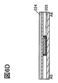
- FIG. 6A is a top view illustrating a method for manufacturing a semiconductor device according to one embodiment of the present invention.
- 6B to 6D are cross-sectional views illustrating a method for manufacturing a semiconductor device according to one embodiment of the present invention.
- FIG. 7A is a top view illustrating a method for manufacturing a semiconductor device according to one embodiment of the present invention.
- 7B to 7D are cross-sectional views illustrating a method for manufacturing a semiconductor device according to one embodiment of the present invention.
- FIG. 8A is a top view illustrating a method for manufacturing a semiconductor device according to one embodiment of the present invention.
- 8B to 8D are cross-sectional views illustrating a method for manufacturing a semiconductor device according to one embodiment of the present invention.
- FIG. 9A is a top view illustrating a method for manufacturing a semiconductor device according to one embodiment of the present invention.
- 9B to 9D are cross-sectional views illustrating a method for manufacturing a semiconductor device according to one embodiment of the present invention.
- FIG. 10A is a top view illustrating a method for manufacturing a semiconductor device according to one embodiment of the present invention.
- 10B to 10D are cross-sectional views illustrating a method for manufacturing a semiconductor device according to one embodiment of the present invention.
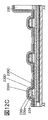
- 11A is a top view illustrating a method for manufacturing a semiconductor device according to one embodiment of the present invention.
- 11B to 11D are cross-sectional views illustrating a method for manufacturing a semiconductor device according to one embodiment of the present invention.
- FIG. 12A is a top view illustrating a method for manufacturing a semiconductor device according to one embodiment of the present invention.
- 12B to 12D are cross-sectional views illustrating a method for manufacturing a semiconductor device according to one embodiment of the present invention.
- FIG. 13A is a top view illustrating a method for manufacturing a semiconductor device according to one embodiment of the present invention.
- 13B to 13D are cross-sectional views illustrating a method for manufacturing a semiconductor device according to one embodiment of the present invention.
- 14A is a top view illustrating a method for manufacturing a semiconductor device according to one embodiment of the present invention.
- 14B to 14D are cross-sectional views illustrating a method for manufacturing a semiconductor device according to one embodiment of the present invention.
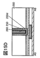
- 15A is a top view illustrating a method for manufacturing a semiconductor device according to one embodiment of the present invention.
- 15B to 15D are cross-sectional views illustrating a method for manufacturing a semiconductor device according to one embodiment of the present invention.
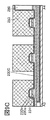
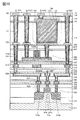
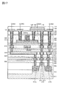
- 16 is a cross-sectional view illustrating the structure of the memory device according to one embodiment of the present invention.
- 17 is a cross-sectional view illustrating the structure of the memory device according to one embodiment of the present invention.
- 18 is a cross-sectional view illustrating the structure of the memory device according to one embodiment of the present invention.
- 19A and 19B are a block diagram and a perspective view illustrating a structural example of a memory device according to one embodiment of the present invention.
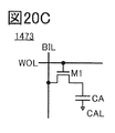
- 20A to 20H are circuit diagrams illustrating a structural example of a memory device according to one embodiment of the present invention.
- 21A and 21B are schematic views of a semiconductor device according to one embodiment of the present invention.
- 22A to 22E are schematic views of a memory device according to one embodiment of the present invention.
- 23A to 23H are diagrams illustrating electronic devices according to one embodiment of the present invention.
- the size, the layer thickness, or the region may be exaggerated for clarity. Therefore, it is not necessarily limited to that scale.
- the drawings schematically show ideal examples and are not limited to the shapes or values shown in the drawings.
- a layer, a resist mask, or the like may be unintentionally reduced due to a process such as etching, but this may not be reflected in the drawing for easy understanding.
- the same reference numerals are commonly used in different drawings for the same portions or portions having similar functions, and repeated description thereof may be omitted.
- the hatch pattern may be the same and may not be given a reference numeral.
- top view also referred to as “plan view”
- perspective view some of the components may be omitted to facilitate understanding of the invention.
- description of some hidden lines may be omitted.
- the ordinal numbers given as the first, second, etc. are used for convenience and do not indicate the order of steps or the order of stacking. Therefore, for example, “first” can be replaced with “second” or “third” as appropriate.
- the ordinal numbers in this specification and the like and the ordinal numbers used to specify one embodiment of the present invention may not match.
- X and Y are connected, a case where X and Y are electrically connected and a case where X and Y function And the case where X and Y are directly connected are disclosed in this specification and the like. Therefore, it is not limited to a predetermined connection relation, for example, the connection relation shown in the drawing or the text, and other than the connection relation shown in the drawing or the text is also disclosed in the drawing or the text.
- X and Y are objects (for example, devices, elements, circuits, wirings, electrodes, terminals, conductive films, layers, etc.).
- a transistor is an element having at least three terminals including a gate, a drain, and a source. And a region (hereinafter, also referred to as a channel formation region) in which a channel is formed between the drain (drain terminal, drain region or drain electrode) and the source (source terminal, source region or source electrode), A current can flow between the source and the drain via the channel formation region.
- a channel formation region refers to a region in which a current mainly flows.
- the functions of the source and drain may be switched when adopting transistors of different polarities or when the direction of current changes during circuit operation. Therefore, in this specification and the like, the terms source and drain can be interchanged in some cases.
- the channel length is, for example, in a top view of a transistor, a region where a semiconductor (or a portion in the semiconductor in which a current flows) and a gate electrode overlap each other in a top view of a transistor, or a source in a channel formation region.
- the channel length does not necessarily have the same value in all regions. That is, the channel length of one transistor may not be set to one value. Therefore, in this specification, the channel length is any one value, the maximum value, the minimum value, or the average value in the channel formation region.
- the channel width is, for example, in a top view of a transistor, a region in which a semiconductor (or a portion in the semiconductor in which a current flows) and a gate electrode overlap with each other in a top view of a transistor, or a channel formation direction in a channel formation region. Is the length of the channel formation region in the vertical direction. Note that in one transistor, the channel width does not necessarily have the same value in all regions. That is, the channel width of one transistor may not be set to one value. Therefore, in this specification, the channel width is any one value, the maximum value, the minimum value, or the average value in the channel formation region.
- a channel width in a region where a channel is actually formed (hereinafter also referred to as an “effective channel width”) and a channel width shown in a top view of the transistor. (Hereinafter, also referred to as “apparent channel width”).
- the effective channel width becomes larger than the apparent channel width, and the effect thereof may not be negligible.
- the proportion of the channel formation region formed in the side surface of the semiconductor may be large. In that case, the effective channel width is larger than the apparent channel width.
- channel width when simply described as channel width, it may indicate an apparent channel width.
- channel width may refer to an effective channel width. Note that the channel length, channel width, effective channel width, apparent channel width, and the like can be determined by analyzing a cross-sectional TEM image or the like.
- the impurities of the semiconductor refer to, for example, components other than the main constituents of the semiconductor.
- an element whose concentration is less than 0.1 atomic% can be said to be an impurity.
- the inclusion of impurities may cause, for example, an increase in the defect level density of the semiconductor and a decrease in crystallinity.
- examples of impurities that change the characteristics of the semiconductor include a Group 1 element, a Group 2 element, a Group 13 element, a Group 14 element, a Group 15 element, and an oxide semiconductor.
- transition metals other than the main component such as hydrogen, lithium, sodium, silicon, boron, phosphorus, carbon, and nitrogen. Water may also function as an impurity.
- oxygen vacancies may be referred to as V 2 O ) may be formed in the oxide semiconductor due to the mixture of impurities, for example.
- silicon oxynitride has a higher oxygen content than nitrogen as its composition. Further, silicon oxynitride has a composition containing more nitrogen than oxygen.
- the term “insulator” can be restated as an insulating film or an insulating layer.
- the term “conductor” can be referred to as a conductive film or a conductive layer.
- the term “semiconductor” can be restated as a semiconductor film or a semiconductor layer.
- parallel means a state in which two straight lines are arranged at an angle of ⁇ 10 degrees to 10 degrees. Therefore, a case of -5 degrees or more and 5 degrees or less is also included.
- substantially parallel means a state in which two straight lines are arranged at an angle of ⁇ 30 degrees or more and 30 degrees or less.
- vertical means a state in which two straight lines are arranged at an angle of 80 degrees or more and 100 degrees or less. Therefore, the case of 85 degrees or more and 95 degrees or less is also included.
- generally vertical means a state in which two straight lines are arranged at an angle of 60 degrees or more and 120 degrees or less.
- a metal oxide is a metal oxide in a broad sense. Metal oxides are classified into oxide insulators, oxide conductors (including transparent oxide conductors), oxide semiconductors (Oxide Semiconductor or simply OS), and the like. For example, when a metal oxide is used for a semiconductor layer of a transistor, the metal oxide may be referred to as an oxide semiconductor. That is, when the term “OS transistor” is used, it can be referred to as a transistor including a metal oxide or an oxide semiconductor.
- normally-off means that when a potential is not applied to the gate or a ground potential is applied to the gate, the drain current per channel width of 1 ⁇ m flowing in the transistor is 1 ⁇ 10 ⁇ at room temperature. It is 20 A or less, 1 ⁇ 10 ⁇ 18 A or less at 85° C., or 1 ⁇ 10 ⁇ 16 A or less at 125° C.
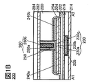
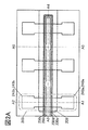
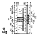
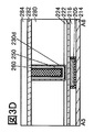
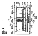
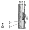
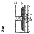
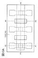
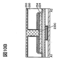
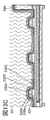
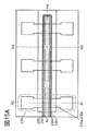
- FIG. 1A to 1D are a top view and a cross-sectional view of a semiconductor device which is one embodiment of the present invention, and the semiconductor device includes a plurality of transistors 200.
- FIG. 1A is a top view of the semiconductor device.
- 1B to 1D are cross-sectional views of the semiconductor device.
- FIG. 1B is a cross-sectional view of a portion indicated by dashed-dotted line A1-A2 in FIG. 1A and also a cross-sectional view of the transistor 200 in the channel length direction.
- 1C is a cross-sectional view of a portion indicated by dashed-dotted line A3-A4 in FIG.
- FIG. 1A which is also a cross-sectional view of the transistor 200 in the channel width direction. Further, FIG. 1D is a cross-sectional view of a portion indicated by an alternate long and short dash line of A5-A6 in FIG. 1A. In the top view of FIG. 1A, some elements are omitted for the sake of clarity.
- a semiconductor device of one embodiment of the present invention includes a plurality of transistors 200, an insulator 214 which functions as an interlayer film, an insulator 216, an insulator 280, an insulator 282, and an insulator 284.
- FIGS. 1A and 1C exemplify a configuration in which the three transistors 200 are arranged in the channel width direction, the invention is not limited to this, and two or four or more transistors 200 are arranged in the channel width direction. It may have been done.
- the transistor 200 includes a conductor 205 provided over a substrate (not shown) and embedded in an insulator 216, and over the insulator 216.
- the insulator 222 provided over the conductor 205, the insulator 224 provided over the insulator 222, and the oxide 230 provided over the insulator 224 (the oxide 230a, the oxide 230b, and The oxide 230c), the insulator 250 provided over the oxide 230, the conductor 260 (the conductor 260a and the conductor 260b) provided over the insulator 250, and one of the top surfaces of the oxide 230b.
- the conductor 240a and the conductor 240b which are in contact with the portion, the upper surface of the insulator 224, the side surface of the oxide 230a, the side surface of the oxide 230b, the side surface and the upper surface of the conductor 240a, and the side surface and the upper surface of the conductor 240b.
- the insulator 254 is arranged.
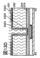
- An opening reaching the oxide 230b is provided in the insulator 280 and the insulator 254.
- the oxide 230c, the insulator 250, and the conductor 260 are arranged in the opening.
- the conductor 260, the insulator 250, and the oxide 230c are provided between the conductor 240a and the conductor 240b.
- the insulator 250 has a region overlapping with a side surface of the conductor 260 and a region overlapping with a bottom surface of the conductor 260.
- the oxide 230c has a region in contact with the oxide 230b, a region overlapping with a side surface of the conductor 260 with the insulator 250 interposed therebetween, and a region overlapping with a bottom surface of the conductor 260 with the insulator 250 interposed therebetween.
- a metal oxide which functions as a semiconductor is preferably used for the oxide 230 including the channel formation region (the oxide 230a, the oxide 230b, and the oxide 230c). ..
- the metal oxide that functions as a semiconductor preferably has a band gap of 2 eV or more, more preferably 2.5 eV or more. By using a metal oxide having a wide band gap in this manner, off-state current of the transistor can be reduced.
- the transistor 200 including a metal oxide in a channel formation region has an extremely small leak current in a non-conduction state, so that a semiconductor device with low power consumption can be provided. Since the metal oxide can be formed by a sputtering method or the like, it can be used for the transistor 200 included in the highly integrated semiconductor device.
- the oxide 230 is disposed over the insulator 224, the oxide 230b, the oxide 230b, the oxide 230b, and the oxide 230b. And an oxide 230c in contact with the top surface.
- the oxide 230a under the oxide 230b diffusion of impurities from the structure formed below the oxide 230a into the oxide 230b can be suppressed.
- the oxide 230c over the oxide 230b diffusion of impurities into the oxide 230b from a structure formed above the oxide 230c can be suppressed.
- the oxide 230 has a structure in which three layers of the oxide 230a, the oxide 230b, and the oxide 230c are stacked; however, the present invention is not limited to this.
- a single layer of the oxide 230b, a two-layer structure of the oxide 230a and the oxide 230b, a two-layer structure of the oxide 230b and the oxide 230c, or a stacked structure of four or more layers may be provided, or oxidation may be performed.
- Each of the object 230a, the oxide 230b, and the oxide 230c may have a laminated structure.
- the oxide 230a and the oxide 230b, and the oxide 230b and the oxide 230c have a common element as a main component in addition to oxygen. Accordingly, the density of defect states at the interface between the oxide 230a and the oxide 230b and the interface between the oxide 230b and the oxide 230c can be reduced. Therefore, the influence of interface scattering on carrier conduction is reduced, and the transistor 200 can obtain a large on-state current and high frequency characteristics.
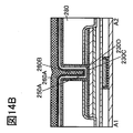
- the conductor 260, the insulator 250, and the oxide 230c may be commonly used between the adjacent transistors 200.
- the oxide 230c overlaps with the conductor 260 with the insulator 250 interposed therebetween, and the oxide 230c is in contact with the oxide 230b of the transistor 200 and the oxide 230b of the transistor 200 adjacent to the transistor 200. Therefore, a parasitic transistor may be formed between the transistor 200 and the transistor 200 adjacent to the transistor 200.
- the oxide 230b of the transistor 200 and the oxide 230b of the transistor 200 adjacent to the transistor 200 are electrically connected to each other and there is a high possibility that a leakage path is generated along the conductor 260.
- the oxide 230c is provided for each transistor 200. That is, the oxide 230c of the transistor 200 and the oxide 230c of the transistor 200 which is adjacent to the transistor 200 are preferably not in contact with each other. Further, the oxide 230c of the transistor 200 and the oxide 230c of the transistor 200 adjacent to the transistor 200 are preferably separated from each other in terms of distance. In other words, the oxide 230c is preferably not arranged between the transistor 200 and the transistor 200 adjacent to the transistor 200.
- the distance between the side edge of the oxide 230c of the transistor 200 and the side edge of the oxide 230c of the transistor 200 adjacent to the transistor 200 is L in the channel width direction of the transistor 200.
- L 1 is made larger than 0 nm.
- L 2 in the channel width direction of the transistor 200, and a side edge portion of the oxide 230a of the transistor 200, to represent the distance between the side edge portion of the oxide 230a of the transistor 200 adjacent to the transistor 200 as a L 2, L 2
- the ratio of L 1 to L 1 (L 1 /L 2 ) is preferably more than 0 and less than 1, more preferably 0.1 or more and 0.9 or less, and still more preferably 0.2 or more and 0.8 or less.
- L 2 may be a distance between a side end portion of the oxide 230b of the transistor 200 and a side end portion of the oxide 230b of the transistor 200 which is adjacent to the transistor 200.
- oxides 230c is a transistor 200, the positional deviation of the arrangement that are not regions between the transistors 200 adjacent to the transistor 200 Even if it occurs, the oxide 230c of the transistor 200 and the oxide 230c of the transistor 200 adjacent to the transistor 200 can be separated from each other in terms of distance.
- the transistor 200 by increasing the ratio of L 1 to the above L 2 (L 1 / L 2 ), the transistor 200, even by narrowing the interval between the transistor 200 adjacent to the transistor 200, the width of the minimum feature size This can be ensured, and further miniaturization or higher integration of the semiconductor device can be achieved.
- the oxide 230c be not provided between the transistor 200 and the transistor 200 adjacent to the transistor 200 in the sidewall of the opening provided in the insulator 280.
- the oxide 230c is provided only in a region of the sidewall of the opening provided in the insulator 280, which overlaps with the oxide 230b, and a region in the vicinity thereof. That is, in the side wall of the opening provided in the insulating member 280, may satisfy a ratio of L 1 to the above L 2 (L 1 / L 2 ). Note that the oxide 230c may not be provided on the sidewall of the opening provided in the insulator 280.
- each of the conductor 260 and the insulator 250 may be commonly used between the adjacent transistors 200.
- the conductor 260 of the transistor 200 has a region continuous with the conductor 260 of the transistor 200 which is adjacent to the transistor 200.
- the conductor 260 of the transistor 200 and the conductor 260 of the transistor 200 adjacent to the transistor 200 are the same film.
- the insulator 250 of the transistor 200 has a region which is provided so as to be continuous with the insulator 250 of the transistor 200 which is adjacent to the transistor 200.
- the insulator 250 of the transistor 200 and the insulator 250 of the transistor 200 adjacent to the transistor 200 are the same film.
- the oxides 230c are independently provided in the transistor 200, and the transistor 200 can obtain a large on-state current and high frequency characteristics. Further, a parasitic transistor can be prevented from being generated between the transistor 200 and the transistor 200 adjacent to the transistor 200, so that the leakage path can be suppressed. Therefore, it is possible to provide a semiconductor device having good electric characteristics and capable of being miniaturized or highly integrated.
- the insulator 250 is provided over the oxide 230c and the insulator 224. That is, the insulator 250 has a region in contact with the insulator 224 between the transistor 200 and the transistor 200 adjacent to the transistor 200.
- the insulator 214 preferably functions as an insulating barrier film which suppresses diffusion of impurities such as water and hydrogen from the substrate side into the transistor 200. Therefore, the insulator 214 has a function of suppressing diffusion of impurities such as hydrogen atoms, hydrogen molecules, water molecules, nitrogen atoms, nitrogen molecules, nitric oxide molecules (N 2 O, NO, NO 2, etc.), and copper atoms. It is preferable to use an insulating material. Alternatively, an insulating material having a function of suppressing diffusion of oxygen (eg, at least one of oxygen atoms and oxygen molecules) is preferably used.
- the function of suppressing the diffusion of impurities or oxygen means the function of suppressing the diffusion of any one or all of the impurities or oxygen.
- a film having a function of suppressing diffusion of hydrogen or oxygen may be a film that hardly permeates hydrogen or oxygen, a film that has low hydrogen or oxygen permeability, a film that has a barrier property against hydrogen or oxygen, or hydrogen or oxygen. May be called a barrier film or the like.
- the barrier film may be referred to as a conductive barrier film.
- the insulator 214 it is preferable to use aluminum oxide, silicon nitride, or the like as the insulator 214. Accordingly, impurities such as water and hydrogen can be suppressed from diffusing from the substrate side to the transistor 200 side with respect to the insulator 214. Alternatively, oxygen contained in the insulator 224 and the like can be suppressed from diffusing toward the substrate side of the insulator 214.
- the insulator 214 may have a stacked structure of two or more layers. In that case, the laminated structure is not limited to the same material, and may be a laminated structure made of different materials. For example, a stack of aluminum oxide and silicon nitride may be used.
- the insulator 214 it is preferable to use silicon nitride formed by a sputtering method. Accordingly, the hydrogen concentration in the insulator 214 can be reduced, and impurities such as water and hydrogen can be further suppressed from diffusing from the substrate side of the insulator 214 to the transistor 200 side.
- the insulator 216 functioning as an interlayer film preferably has a lower dielectric constant than the insulator 214.
- a material having a low dielectric constant as the interlayer film, it is possible to reduce the parasitic capacitance generated between the wirings.
- silicon oxide, silicon oxynitride, silicon nitride oxide, silicon nitride, silicon oxide added with fluorine, silicon oxide added with carbon, silicon oxide added with carbon and nitrogen, silicon oxide having holes Etc. may be appropriately used.
- the insulator 216 has a low hydrogen concentration and a region where oxygen is present in excess of the stoichiometric composition (hereinafter also referred to as an excess oxygen region) or oxygen released by heating (hereinafter also referred to as excess oxygen). .) is preferable.
- the insulator 216 silicon oxide formed by a sputtering method is preferably used. Accordingly, hydrogen can be prevented from entering the oxide 230, or oxygen can be supplied to the oxide 230 and oxygen vacancies in the oxide 230 can be reduced. Therefore, it is possible to provide a transistor in which variation in electrical characteristics is suppressed, stable electrical characteristics are obtained, and reliability is improved.
- the insulator 216 may have a laminated structure.
- an insulator similar to the insulator 214 may be provided at least in a portion in contact with the side surface of the conductor 205.
- oxidation of the conductor 205 due to oxygen contained in the insulator 216 can be suppressed.
- the conductor 205 can suppress a decrease in the amount of oxygen contained in the insulator 216.
- the conductor 205 may function as the second gate electrode.
- the threshold voltage (Vth) of the transistor 200 can be controlled by changing the potential applied to the conductor 205 independently of the potential applied to the conductor 260 and without changing the potential.
- Vth of the transistor 200 can be further increased and off-state current can be reduced. Therefore, applying a negative potential to the conductor 205 can reduce the drain current when the potential applied to the conductor 260 is 0 V, as compared to the case where no potential is applied.
- the conductor 205 is arranged so as to overlap with the oxide 230 and the conductor 260.
- the conductor 205 is preferably embedded in the insulator 214 or the insulator 216.
- the conductor 205 is preferably provided larger than a channel formation region in the oxide 230 as illustrated in FIG. 1B.
- the conductor 205 is preferably extended also in a region outside the end portion of the oxide 230 which intersects with the channel width direction. That is, it is preferable that the conductor 205 and the conductor 260 overlap with each other with the insulator provided outside the side surface of the oxide 230 in the channel width direction.
- the electric field of the conductor 260 functioning as the first gate electrode and the electric field of the conductor 205 functioning as the second gate electrode electrically surround the channel formation region of the oxide 230.
- a structure of a transistor which electrically surrounds a channel formation region by an electric field of a first gate and a second gate is referred to as a surrounded channel (S-channel) structure.
- a transistor having an S-channel structure refers to a transistor structure that electrically surrounds a channel formation region by electric fields of one and the other of a pair of gate electrodes.
- the side surface and the periphery of the oxide 230 which is in contact with the conductors 240a and 240b functioning as a source electrode and a drain electrode are i-type like the channel formation region. It has characteristics. Further, since the side surface and the periphery of the oxide 230 which is in contact with the conductor 240a and the conductor 240b is in contact with the insulator 280, it can be i-type as in the channel formation region.
- I-form can be treated as the same as high-purity intrinsic described later.
- the S-channel structure disclosed in this specification and the like is different from the Fin-type structure and the planar-type structure.
- the conductor 205 is stretched to function as a wiring.
- the invention is not limited to this, and a conductor functioning as a wiring may be provided below the conductor 205. Further, it is not always necessary to provide one conductor 205 for each transistor. For example, the conductor 205 may be shared by a plurality of transistors.
- the transistor 200 has a structure in which the first conductor of the conductor 205 and the second conductor of the conductor 205 are stacked, but the present invention is not limited to this.
- the conductor 205 may have a single-layer structure or a stacked structure including three or more layers.
- an ordinal number may be given in the order of formation to distinguish them.
- the first conductor of the conductor 205 includes impurities such as hydrogen atoms, hydrogen molecules, water molecules, nitrogen atoms, nitrogen molecules, nitric oxide molecules (N 2 O, NO, NO 2, etc.), and copper atoms. It is preferable to use a conductive material having a function of suppressing diffusion. Alternatively, a conductive material having a function of suppressing diffusion of oxygen (eg, at least one of oxygen atoms and oxygen molecules) is preferably used.
- the first conductor of the conductor 205 may be a single layer or a stacked layer of the above conductive material.
- the first conductor of the conductor 205 may be a stack of tantalum, tantalum nitride, ruthenium, or ruthenium oxide and titanium or titanium nitride.
- the second conductor of the conductor 205 is illustrated as a single layer, it may have a stacked structure, for example, a stack of titanium or titanium nitride and the conductive material.
- the insulator 222 and the insulator 224 function as a gate insulator.
- the insulator 222 preferably has a function of suppressing diffusion of hydrogen (for example, at least one of hydrogen atoms and hydrogen molecules).
- the insulator 222 preferably has a function of suppressing diffusion of oxygen (eg, at least one of oxygen atoms and oxygen molecules).
- the insulator 222 preferably has a function of suppressing diffusion of one or both of hydrogen and oxygen as compared with the insulator 224.
- an insulator containing an oxide of one or both of aluminum and hafnium, which are insulating materials, may be used.
- aluminum oxide, hafnium oxide, an oxide containing aluminum and hafnium (hafnium aluminate), or the like is preferably used.
- the insulator 222 releases oxygen from the oxide 230 to the substrate side and diffuses impurities such as hydrogen from the peripheral portion of the transistor 200 to the oxide 230. Function as a layer that suppresses Therefore, by providing the insulator 222, diffusion of impurities such as hydrogen into the inside of the transistor 200 and generation of oxygen vacancies in the oxide 230 can be suppressed.
- the conductor 205 can be prevented from reacting with the insulator 224 and oxygen contained in the oxide 230.
- aluminum oxide, bismuth oxide, germanium oxide, niobium oxide, silicon oxide, titanium oxide, tungsten oxide, yttrium oxide, or zirconium oxide may be added to the insulator.
- these insulators may be nitrided.
- the insulator 222 may be formed by stacking silicon oxide, silicon oxynitride, or silicon nitride on these insulators.
- the insulator 222 is made of, for example, aluminum oxide, hafnium oxide, tantalum oxide, zirconium oxide, lead zirconate titanate (PZT), strontium titanate (SrTiO 3 ), (Ba,Sr)TiO 3 (BST), or the like.
- An insulator including a so-called high-k material may be used in a single layer or a stacked layer. As transistors become finer and more highly integrated, thinning of the gate insulator may cause problems such as leakage current. By using a high-k material for the insulator functioning as a gate insulator, it is possible to reduce the gate potential during transistor operation while maintaining the physical film thickness.
- the insulator 224 in contact with the oxide 230 desorb oxygen by heating.
- the insulator 224 may be formed using silicon oxide, silicon oxynitride, or the like as appropriate.
- the insulator 224 it is preferable to use an oxide material from which part of oxygen is released by heating, in other words, an insulator material having an excess oxygen region.
- the oxide film that desorbs oxygen by heating means that the amount of desorbed oxygen molecules is 1.0 ⁇ 10 18 molecules/cm 3 or more, preferably 1.0 ⁇ 10 19 molecules, in TDS (Thermal Desorption Spectroscopy) analysis. /Cm 3 or more, more preferably 2.0 ⁇ 10 19 molecules/cm 3 or more, or 3.0 ⁇ 10 20 molecules/cm 3 or more.
- the surface temperature of the film during the TDS analysis is preferably 100° C. or higher and 700° C. or lower, or 100° C. or higher and 400° C. or lower.
- any one or more of heat treatment, microwave treatment, and RF treatment may be performed by contacting the oxide 230 with the insulator having the excess oxygen region.
- water or hydrogen in the oxide 230 can be removed.
- a reaction bond defects that contains hydrogen to an oxygen vacancy (V O H) is cut occurs, a reaction occurs that when other words "V O H ⁇ V O + H", dehydrogenation Can be converted.
- Part of the hydrogen generated at this time may be combined with oxygen and converted into H 2 O to be removed from the oxide 230 or the insulator in the vicinity of the oxide 230.
- part of hydrogen may be diffused or captured (also referred to as gettering) in the conductor 240a and the conductor 240b.
- the microwave treatment for example, it is preferable to use an apparatus having a power source for generating high density plasma or an apparatus having a power source for applying RF to the substrate side.
- a gas containing oxygen and using high-density plasma high-density oxygen radicals can be generated, and by applying RF to the substrate side, oxygen radicals generated by high-density plasma can be generated.
- the pressure may be 133 Pa or higher, preferably 200 Pa or higher, more preferably 400 Pa or higher.
- oxygen and argon are used, and the oxygen flow rate ratio (O 2 /(O 2 +Ar)) is 50% or less, preferably 10% or more 30 % Or less is recommended.
- heat treatment is preferably performed with the surface of the oxide 230 exposed.
- the heat treatment may be performed at 100 °C to 450 °C inclusive, more preferably 350 °C to 400 °C inclusive, for example.
- the heat treatment is performed in an atmosphere of nitrogen gas or an inert gas, or an atmosphere containing an oxidizing gas in an amount of 10 ppm or more, 1% or more, or 10% or more.
- the heat treatment is preferably performed in an oxygen atmosphere.
- oxygen can be supplied to the oxide 230 to reduce oxygen vacancies (V 2 O 3 ).
- the heat treatment may be performed under reduced pressure.
- the heat treatment may be performed in an atmosphere containing an oxidizing gas in an amount of 10 ppm or higher, 1% or higher, or 10% or higher in order to supplement desorbed oxygen after the heat treatment is performed in a nitrogen gas or inert gas atmosphere.
- heat treatment may be performed in an atmosphere containing an oxidizing gas in an amount of 10 ppm or more, 1% or more, or 10% or more, and then continuously performed in an atmosphere of nitrogen gas or an inert gas.
- the insulator 224 preferably has a low hydrogen concentration and has an excess oxygen region or excess oxygen.
- a material similar to that of the insulator 216 may be used.
- the insulator 222 and the insulator 224 may have a laminated structure of two or more layers.
- the laminated structure is not limited to the same material, and may be a laminated structure made of different materials.
- the oxide 230 examples include In-M-Zn oxide (the element M is aluminum, gallium, yttrium, tin, copper, vanadium, beryllium, boron, titanium, iron, nickel, germanium, zirconium, molybdenum, lanthanum, cerium). , One kind or plural kinds selected from neodymium, hafnium, tantalum, tungsten, magnesium and the like) may be used. Alternatively, as the oxide 230, an In—Ga oxide or an In—Zn oxide may be used. Note that when it is desired to increase the on-state current of the transistor 200, it is preferable to use an In—Zn oxide for the oxide 230.
- an In—Zn oxide is used for the oxide 230
- a stacked-layer structure in which an In—Zn oxide is used for the oxide 230a and an In—M—Zn oxide is used for the oxide 230b and the oxide 230c, or an oxide is used.
- a stacked structure in which an In-M-Zn oxide is used for the object 230a and an In-Zn oxide is used for either one of the oxide 230b and the oxide 230c can be given.
- the oxide 230 preferably has a laminated structure of a plurality of oxide layers having different chemical compositions.
- the atomic ratio of the element M to the metal element serving as the main component is larger than that of the element M to the metal element serving as the main component in the metal oxide used for the oxide 230b. It is preferably larger than the atomic number ratio.
- the atomic ratio of the element M to In is preferably higher than the atomic ratio of the element M to In in the metal oxide used for the oxide 230b.
- the atomic ratio of In to the element M is preferably higher than the atomic ratio of In to the element M in the metal oxide used for the oxide 230a.
- the oxide 230c a metal oxide which can be used for the oxide 230a or the oxide 230b can be used.
- the oxide 230b and the oxide 230c preferably have crystallinity.
- a CAAC-OS c-axis aligned crystalline oxide semiconductor
- An oxide having crystallinity such as CAAC-OS has few impurities and defects (such as oxygen vacancies), has high crystallinity, and has a dense structure. Therefore, extraction of oxygen from the oxide 230b by the source electrode or the drain electrode can be suppressed. Accordingly, extraction of oxygen from the oxide 230b can be reduced even when heat treatment is performed, so that the transistor 200 is stable against a high temperature (so-called thermal budget) in a manufacturing process.
- CAAC-OS As the oxide 230c, it is preferable to use CAAC-OS as the oxide 230c, and it is preferable that a c-axis of a crystal included in the oxide 230c is oriented substantially perpendicular to a formation surface or an upper surface of the oxide 230c.
- the CAAC-OS has a property of easily moving oxygen in a direction perpendicular to the c-axis. Therefore, the oxygen contained in the oxide 230c can be efficiently supplied to the oxide 230b.
- the conduction band lower ends of the oxides 230a and 230c are preferably closer to the vacuum level than the conduction band lower ends of the oxide 230b.
- the electron affinity of the oxide 230a and the oxide 230c is preferably smaller than that of the oxide 230b.
- the oxide 230c is preferably a metal oxide that can be used for the oxide 230a.
- the main path of carriers is the oxide 230b.
- the lower end of the conduction band changes gently at the junction of the oxide 230a, the oxide 230b, and the oxide 230c.
- the bottoms of the conduction bands at the junctions of the oxide 230a, the oxide 230b, and the oxide 230c are continuously changed or continuously joined.
- the oxide 230a and the oxide 230b and the oxide 230b and the oxide 230c have a common element other than oxygen as a main component, whereby a mixed layer with low defect level density can be formed. ..
- the oxide 230b is an In—Ga—Zn oxide
- an In—Ga—Zn oxide, a Ga—Zn oxide, gallium oxide, or the like may be used as the oxide 230a and the oxide 230c.
- In:Ga:Zn 4:2:3 [atomic ratio]
- Ga:Zn 2:1 [atomic] [Number ratio]
- the above atomic ratio is not limited to the atomic ratio of the formed metal oxide, and the atomic ratio of a sputtering target used for forming the metal oxide is not limited. May be
- the oxide 230a and the oxide 230c having the above structures, the density of defect states at the interface between the oxide 230a and the oxide 230b and the interface between the oxide 230b and the oxide 230c can be reduced. Therefore, the influence of interface scattering on carrier conduction is reduced, and the transistor 200 can obtain a large on-state current and high frequency characteristics.
- Examples of the conductor 240a and the conductor 240b include a nitride containing tantalum, a nitride containing titanium, a nitride containing molybdenum, a nitride containing tungsten, a nitride containing tantalum and aluminum, and titanium and aluminum. It is preferable to use a nitride or the like. In one aspect of the present invention, a nitride containing tantalum is particularly preferable. Further, for example, ruthenium oxide, ruthenium nitride, an oxide containing strontium and ruthenium, an oxide containing lanthanum and nickel, or the like may be used. These materials are preferable because they are conductive materials that are difficult to oxidize or materials that maintain conductivity even when absorbing oxygen.
- oxygen in the oxide 230b may be diffused into the conductor 240a and the conductor 240b and the conductor 240a and the conductor 240b may be oxidized. is there. Oxidation of the conductors 240a and 240b is likely to reduce the conductivity of the conductors 240a and 240b. Note that diffusion of oxygen in the oxide 230b to the conductor 240a and the conductor 240b can be restated as absorption of oxygen in the oxide 230b by the conductor 240a and the conductor 240b.
- the oxide 230b diffuses into the conductors 240a and 240b, so that a layer is formed between the conductor 240a and the oxide 230b and between the conductor 240b and the oxide 230b.
- the layer contains more oxygen than the conductor 240a or the conductor 240b, it is presumed that the layer has an insulating property.
- the three-layer structure of the conductor 240a or the conductor 240b, the layer, and the oxide 230b can be regarded as a three-layer structure including a metal-insulator-semiconductor and a MIS (Metal-Insulator-Semiconductor). ) Structure or a diode junction structure mainly composed of MIS structure.
- hydrogen contained in the oxide 230b or the like may diffuse into the conductor 240a or the conductor 240b.
- hydrogen contained in the oxide 230b or the like may diffuse into the conductor 240a or the conductor 240b.
- a nitride containing tantalum for the conductor 240a and the conductor 240b hydrogen contained in the oxide 230b or the like is easily diffused into the conductor 240a or the conductor 240b, and the diffused hydrogen is not included in the conductor.
- 240a or the conductor 240b may be combined with nitrogen. That is, hydrogen contained in the oxide 230b or the like may be absorbed by the conductor 240a or the conductor 240b.
- a curved surface between the side surface of the conductor 240a and the upper surface of the conductor 240a and between the side surface of the conductor 240b and the upper surface of the conductor 240b. That is, the end portion of the side surface and the end portion of the upper surface may be curved (hereinafter, also referred to as round shape).
- the curved surface has, for example, a radius of curvature of 3 nm or more and 10 nm or less, preferably 5 nm or more and 6 nm or less at each of the end portions of the conductor 240a and the conductor 240b.
- the insulator 254 is in contact with the top surface and the side surface of the conductor 240a, the top surface and the side surface of the conductor 240b, the side surfaces of the oxides 230a and 230b, and part of the top surface of the insulator 224 as illustrated in FIG. 1B.
- the insulator 280 is separated from the insulator 224, the oxide 230a, and the oxide 230b by the insulator 254.
- the insulator 254 preferably has a function of suppressing diffusion of one or both of hydrogen and oxygen, like the insulator 222.
- the insulator 254 preferably has a function of suppressing diffusion of one or both of hydrogen and oxygen as compared with the insulator 224 and the insulator 280. Accordingly, hydrogen contained in the insulator 280 can be suppressed from diffusing into the oxide 230a and the oxide 230b.
- diffusion of impurities such as water and hydrogen from the outside into the insulator 224 and the oxide 230 is suppressed. can do. Therefore, the transistor 200 can have favorable electrical characteristics and reliability.
- the insulator 254 is preferably formed by a sputtering method.
- oxygen can be added in the vicinity of a region of the insulator 224 which is in contact with the insulator 254. Accordingly, oxygen can be supplied to the oxide 230 from the region through the insulator 224.
- the insulator 254 has a function of suppressing upward diffusion of oxygen, whereby oxygen can be prevented from diffusing from the oxide 230 to the insulator 280.
- the insulator 222 has a function of suppressing downward diffusion of oxygen, whereby oxygen can be prevented from diffusing from the oxide 230 to the substrate side. In this manner, oxygen is supplied to the channel formation region of the oxide 230. Accordingly, oxygen vacancies in the oxide 230 can be reduced and the normally-on state of the transistor can be suppressed.
- the insulator 254 for example, an insulator containing an oxide of one or both of aluminum and hafnium may be formed.
- the insulator 254 is preferably formed by using an atomic layer deposition (ALD: Atomic Layer Deposition) method. Since the ALD method is a film formation method with favorable coverage, it is possible to prevent step breaks and the like from being formed due to unevenness of the insulator 254.
- ALD Atomic Layer Deposition
- an insulator containing aluminum nitride may be used. Accordingly, a film having excellent insulating properties and excellent thermal conductivity can be obtained, so that heat dissipation of heat generated when the transistor 200 is driven can be improved.
- silicon nitride, silicon nitride oxide, or the like can be used.
- an oxide containing gallium may be used as the insulator 254.
- An oxide containing gallium is preferable because it may have a function of suppressing diffusion of one or both of hydrogen and oxygen.
- gallium oxide, gallium zinc oxide, indium gallium zinc oxide, or the like can be used as the oxide containing gallium.
- indium gallium zinc oxide is used as the insulator 254, a higher atomic ratio of gallium to indium is preferable. By increasing the atomic ratio, the insulating property of the oxide can be increased.
- the insulator 254 can have a multi-layer structure of two or more layers.
- the lower layer and the upper layer of the insulator 254 can be formed by the above method, and the lower layer and the upper layer of the insulator 254 can be formed by the same method. May be used, or different methods may be used.
- a lower layer of the insulator 254 may be formed by a sputtering method in an atmosphere containing oxygen, and then an upper layer of the insulator 254 may be formed by an ALD method. Since the ALD method is a film forming method having a good covering property, it is possible to prevent step breaks and the like from being formed due to the unevenness of the first layer.
- the above materials can be used for the lower layer and the upper layer of the insulator 254, and the lower layer and the upper layer of the insulator 254 may be the same material or different materials.
- a stacked-layer structure of silicon oxide, silicon oxynitride, silicon nitride oxide, or silicon nitride and an insulator having a function of suppressing permeation of impurities such as hydrogen and oxygen may be employed.
- an insulator having a function of suppressing the permeation of impurities such as hydrogen and oxygen for example, an insulator containing an oxide of one or both of aluminum and hafnium can be used.
- the insulator 250 functions as a gate insulator.
- the insulator 250 is preferably provided in contact with at least part of the oxide 230c.
- silicon oxide, silicon oxynitride, silicon nitride oxide, silicon nitride, fluorine-added silicon oxide, carbon-added silicon oxide, carbon-nitrogen-added silicon oxide, vacant silicon oxide, or the like is used.
- silicon oxide and silicon oxynitride are preferable because they are stable to heat.
- the insulator 250 is preferably formed using an insulator from which oxygen is released by heating.
- an insulator from which oxygen is released by heating As the insulator 250 in contact with at least part of the oxide 230c, oxygen is effectively supplied to the channel formation region of the oxide 230b and the oxide 230b is removed. Oxygen deficiency in the channel formation region can be reduced. Therefore, it is possible to provide a transistor in which variation in electrical characteristics is suppressed, stable electrical characteristics are obtained, and reliability is improved.
- the concentration of impurities such as water and hydrogen in the insulator 250 be reduced.
- the thickness of the insulator 250 is preferably 1 nm or more and 20 nm or less.
- microwave treatment is preferably performed in an atmosphere containing oxygen and under reduced pressure.
- the electric field due to the microwave is provided in the insulator 250 and the oxide 230, and be divided into insulator 250, and the V O H in the oxide 230 on the V O and hydrogen it can.
- part of the hydrogen which is separated may be combined with oxygen to be removed as H 2 O from the insulator 250 and the oxide 230.
- part of hydrogen may be gettered to the conductor 240a and the conductor 240b.
- the microwave treatment the hydrogen concentration in the insulator 250 and the oxide 230 can be reduced. Further, it is possible to repair or compensate for V O by oxygen is supplied to the V O which may be present after dividing the V O H in the oxide 230 on the V O and hydrogen.
- the heat treatment may be performed while maintaining the reduced pressure state.
- hydrogen in the insulator 250 and the oxide 230 can be efficiently removed.
- hydrogen in the insulator 250 and the oxide 230 can be removed more efficiently. Note that the step of performing heat treatment may be repeated a plurality of times with the reduced pressure maintained after the microwave treatment.
- the film quality of the insulator 250 is modified, so that diffusion of hydrogen, water, impurities, and the like can be suppressed. Therefore, diffusion of hydrogen, water, or impurities into the oxide 230 through the insulator 250 is suppressed by a post-process such as formation of a conductive film to be the conductor 260 or a post-process such as heat treatment. be able to.
- a transistor including such a metal oxide as a channel formation region can have normally-off characteristics, and a semiconductor device having favorable electric characteristics and reliability can be formed.
- a metal oxide may be provided between the insulator 250 and the conductor 260.
- the metal oxide preferably suppresses diffusion of oxygen from the insulator 250 to the conductor 260.
- diffusion of oxygen from the insulator 250 to the conductor 260 is suppressed. That is, a decrease in the amount of oxygen supplied to the oxide 230 can be suppressed.
- oxidation of the conductor 260 due to oxygen in the insulator 250 can be suppressed.
- the above metal oxide may have a function as a part of the gate insulator. Therefore, when silicon oxide, silicon oxynitride, or the like is used for the insulator 250, the metal oxide is preferably a high-k material having a high relative dielectric constant.
- the gate insulator has a stacked structure of the insulator 250 and the above metal oxide, a stacked structure which is stable to heat and has a high relative dielectric constant can be obtained. Therefore, it is possible to reduce the gate potential applied during transistor operation while maintaining the physical film thickness of the gate insulator. In addition, it is possible to reduce the equivalent oxide film thickness (EOT) of the insulator that functions as the gate insulator.
- EOT equivalent oxide film thickness
- a metal oxide containing one or more selected from hafnium, aluminum, gallium, yttrium, zirconium, tungsten, titanium, tantalum, nickel, germanium, magnesium and the like can be used.
- an insulator containing an oxide of one or both of aluminum and hafnium it is preferable to use an insulator containing an oxide of one or both of aluminum and hafnium.
- the metal oxide may have a function as a part of the first gate electrode.
- a metal oxide that can be used as the oxide 230 can be used as the above metal oxide. In that case, by forming a film of the conductor 260 by a sputtering method, the electric resistance value of the metal oxide can be reduced to form a conductor.
- the on-state current of the transistor 200 can be improved without weakening the influence of the electric field from the conductor 260.
- the leakage current between the conductor 260 and the oxide 230 is maintained. Can be suppressed.
- the physical distance between the conductor 260 and the oxide 230 and the electric field strength applied from the conductor 260 to the oxide 230 can be reduced. It can be easily adjusted appropriately.
- the conductor 260 preferably has a conductor 260a and a conductor 260b arranged on the conductor 260a.
- the conductor 260a is preferably arranged so as to surround the bottom surface and the side surface of the conductor 260b.
- a conductive material having a function of suppressing diffusion of impurities such as hydrogen atoms, hydrogen molecules, water molecules, nitrogen atoms, nitrogen molecules, nitric oxide molecules, and copper atoms.
- a conductive material having a function of suppressing diffusion of oxygen eg, at least one of oxygen atoms and oxygen molecules is preferably used.
- the conductor 260a has a function of suppressing diffusion of oxygen, it is possible to suppress the conductivity of the conductor 260b from being reduced due to the oxygen contained in the insulator 250 from oxidizing the conductor 260b.
- a conductive material having a function of suppressing diffusion of oxygen for example, tantalum, tantalum nitride, ruthenium, ruthenium oxide, or the like is preferably used.
- the conductor 260 also functions as a wiring, it is preferable to use a conductor having high conductivity.
- the conductor 260b can be formed using a conductive material containing tungsten, copper, or aluminum as its main component.
- the conductor 260b may have a stacked structure, for example, a stacked structure of titanium or titanium nitride and the above conductive material.
- the conductor 260 is shown as a two-layer structure of a conductor 260a and a conductor 260b, but may have a single-layer structure or a stacked structure of three or more layers.
- the conductor 260 is formed in a self-aligned manner so as to fill the opening formed in the insulator 280 or the like.
- the conductor 260 can be reliably arranged in the region between the conductor 240a and the conductor 240b without alignment.
- the top surface of the conductor 260 is substantially aligned with the top surface of the insulator 250 and the top surface of the oxide 230c.
- a bottom surface of a region of the conductor 260 where the conductor 260 and the oxide 230b do not overlap is preferably lower than a bottom surface of the oxide 230b.
- the conductor 260 functioning as a gate electrode covers a side surface and an upper surface of a channel formation region of the oxide 230b with the insulator 250 or the like interposed therebetween, so that an electric field of the conductor 260 is applied to the channel formation region of the oxide 230b. It becomes easy to act on the whole. Therefore, the on-state current of the transistor 200 can be increased and frequency characteristics can be improved.
- the insulator 280 is provided on the insulator 224, the oxide 230, the conductor 240a, the conductor 240b, and the insulator 254. Further, the upper surface of the insulator 280 may be flattened.
- the insulator 280 functioning as an interlayer film preferably has a low dielectric constant.
- the insulator 280 is preferably provided using a material similar to that of the insulator 216, for example.
- silicon oxide and silicon oxynitride are preferable because they are thermally stable.
- a material such as silicon oxide, silicon oxynitride, or silicon oxide having pores is preferable because a region containing oxygen which is released by heating can be easily formed.
- an insulator containing oxygen for the insulator 280.
- the insulator 280 preferably has a low hydrogen concentration and has an excess oxygen region or excess oxygen, and may be provided using a material similar to that of the insulator 216, for example.
- the insulator 280 may have a structure in which the above materials are stacked, for example, silicon oxide formed by a sputtering method and a chemical vapor deposition (CVD) method stacked thereover. A laminated structure of filmed silicon oxynitride may be used. In addition, silicon nitride may be stacked further thereon.
- the insulator 282 preferably functions as an insulating barrier film which suppresses diffusion of impurities such as water and hydrogen from above into the insulator 280.
- the insulator 282 preferably has a low hydrogen concentration and has a function of suppressing diffusion of hydrogen, like the insulator 214 and the like.
- the insulator 282 is preferably in contact with the top surfaces of the conductor 260, the insulator 250, and the oxide 230c.
- impurities such as hydrogen contained in the insulator 284 and the like can be prevented from entering the insulator 250. Therefore, adverse effects on the electrical characteristics of the transistor and the reliability of the transistor can be suppressed.
- the insulator 284 preferably has a low dielectric constant similarly to the insulator 216 and the like.
- the insulator 284 preferably has a reduced concentration of impurities such as water and hydrogen in the film, like the insulator 224 and the like.
- a plug electrically connected to the transistor 200 or a conductor functioning as a wiring may be provided.
- the resistivity is 1.0 ⁇ 10 13 ⁇ cm or more and 1.0 ⁇ 10 15 ⁇ cm or less, preferably 5.0 ⁇ 10 13 ⁇ cm or more and 5.0 ⁇ 10 14 ⁇ cm or less so as to cover the conductor.
- FIGS. 2A, 3A, and 4A show top views.
- FIGS. 2B, 3B, and 4B are cross-sectional views corresponding to the portions indicated by the one-dot chain line of A1-A2 in FIGS. 2A, 3A, and 4A, respectively.
- FIGS. 2C, 3C, and 4C are cross-sectional views corresponding to the portions indicated by dashed-dotted line A3-A4 in FIGS. 2A, 3A, and 4A, respectively.
- FIGS. 2D, 3D, and 4D are cross-sectional views corresponding to the portions indicated by dashed-dotted line A5-A6 in FIGS. 2A, 3A, and 4A, respectively.
- FIGS. 2A, 3A, and 4A In the top views of FIGS. 2A, 3A, and 4A, some elements have been omitted for clarity.
- the semiconductor device shown in FIGS. 2A to 2D is a modification of the semiconductor device shown in FIGS. 1A to 1D.
- the semiconductor devices illustrated in FIGS. 2A to 2D are different from the semiconductor devices illustrated in FIGS. 1A to 1D in that they include the oxide 230d and the oxide 243 (the oxide 243a and the oxide 243b).
- the oxide 230d of the transistor 200 has a region provided continuously to the oxide 230d of the transistor 200 adjacent to the transistor 200.
- the oxide 230d is insulated. It has a region in contact with the body 224.
- the oxide 230d preferably contains at least one of the metal elements constituting the metal oxide used for the oxide 230c, and more preferably contains all the metal elements.
- an In-Ga-Zn oxide or an In-Zn oxide may be used as the oxide 230c
- an In-Ga-Zn oxide, a Ga-Zn oxide, or gallium oxide may be used as the oxide 230d. Accordingly, the density of defect states at the interface between the oxide 230c and the oxide 230d can be reduced.
- the bottoms of the conduction bands of the oxides 230a and 230d be closer to the vacuum level than the bottoms of the conduction bands of the oxides 230b and 230c.
- the electron affinity of the oxide 230a and the oxide 230d is preferably smaller than the electron affinity of the oxide 230b and the oxide 230c.
- the oxide 230d be a metal oxide that can be used for the oxide 230a
- the oxide 230c be a metal oxide that can be used for the oxide 230b. At this time, not only the oxide 230b but also the oxide 230c may be a main carrier main path.
- a metal oxide or gallium oxide having an [atomic ratio] may be used. Accordingly, the density of defect states at the interface between the oxide 230c and the oxide 230d can be reduced.
- the oxide 230d is preferably a metal oxide that suppresses diffusion or permeation of oxygen as compared with the oxide 230c.
- oxygen contained in the insulator 280 can be suppressed from diffusing into the insulator 250. Therefore, the oxygen can be efficiently supplied to the oxide 230b through the oxide 230c.
- the atomic ratio of In to the metal element serving as the main component is smaller than the atomic ratio of In to the metal element serving as the main component in the metal oxide used for the oxide 230c.
- In can be suppressed from diffusing to the insulator 250 side.
- the insulator 250 functions as a gate insulator; therefore, if In is mixed in the insulator 250 or the like, the characteristics of the transistor are deteriorated. Therefore, by providing the oxide 230d between the oxide 230c and the insulator 250, a highly reliable semiconductor device can be provided.
- the semiconductor device illustrated in FIGS. 2A to 2D includes an oxide 243 (an oxide 243a and an oxide 243b) having a function of suppressing oxygen permeation between the conductor 240a or the conductor 240b and the oxide 230.
- an oxide 243 an oxide 243a and an oxide 243b having a function of suppressing oxygen permeation between the conductor 240a or the conductor 240b and the oxide 230.
- the oxide 243 having a function of suppressing permeation of oxygen between the conductor 240a or the conductor 240b functioning as a source electrode or a drain electrode and the oxide 230b, the conductor 240a or the conductor 240b, It is preferable because the electrical resistance between the oxide 230b and the oxide 230b is reduced. With such a structure, electric characteristics of the transistor 200 and reliability of the transistor 200 can be improved.
- a metal oxide containing the element M may be used.
- the element M is preferably aluminum, gallium, yttrium, or tin.
- the oxide 243 preferably has a higher concentration of the element M than the oxide 230b.
- gallium oxide may be used as the oxide 243.
- a metal oxide such as an In-M-Zn oxide may be used.
- the atomic ratio of the element M to In is preferably higher than the atomic ratio of the element M to In in the metal oxide used for the oxide 230b.
- the thickness of the oxide 243 is preferably 0.5 nm or more and 5 nm or less, more preferably 1 nm or more and 3 nm or less, and further preferably 1 nm or more and 2 nm or less. Further, the oxide 243 preferably has crystallinity. When the oxide 243 has crystallinity, release of oxygen in the oxide 230 can be suppressed appropriately. For example, if the oxide 243 has a hexagonal crystal structure or the like, release of oxygen in the oxide 230 can be suppressed in some cases.
- the semiconductor device shown in FIGS. 3A to 3D is a modification of the semiconductor device shown in FIGS. 2A to 2D.
- the semiconductor device illustrated in FIGS. 3A to 3D is different in the shape of the oxide 230c from the semiconductor devices illustrated in FIGS. 2A to 2D.
- the region where the oxide 230c and the top surface of the insulator 224 are in contact with each other in the channel width direction is narrower than the semiconductor devices illustrated in FIGS. 2A to 2D. Is.
- the configuration ratio of L 1 to the above L 2 (L 1 / L 2 ) is greater.
- the oxide 230c other than the region overlapping with the oxide 230b and the vicinity thereof is removed.
- the oxide 230c is left in the region overlapping with the oxide 230b and the vicinity thereof.
- the bottom surface of the conductor 260 in a region which does not overlap with the oxide 230b becomes lower, and a region where the conductor 260 covers the side surface and the top surface of the oxide 230b with the oxide 230c and the insulator 250 spreads.
- the electric field of 260 easily acts on the entire channel formation region of the oxide 230b. Therefore, the on-state current of the transistor 200 can be increased and frequency characteristics can be improved.
- the semiconductor device illustrated in FIGS. 3A to 3D is different from the semiconductor devices illustrated in FIGS. 2A to 2D in that the semiconductor device does not include the insulator 254 but includes the insulator 245a and the insulator 245b.
- the insulator 245a and the insulator 245b are preferably in contact with the upper surfaces of the conductor 240a and the conductor 240b, respectively, as shown in FIG. 3B.
- the insulator 245a and the insulator 245b preferably function as barrier layers. With such a structure, absorption of excess oxygen included in the insulator 280 by the conductor 240a and the conductor 240b can be suppressed. Further, by suppressing the oxidation of the conductor 240a and the conductor 240b, an increase in contact resistance between the transistor 200 and the wiring can be suppressed. Therefore, the transistor 200 can have favorable electrical characteristics and reliability.
- the insulator 245a and the insulator 245b have a function of suppressing diffusion of oxygen.
- the insulator 245a and the insulator 245b preferably have a function of suppressing diffusion of oxygen as compared with the insulator 280.
- an insulator containing an oxide of one or both of aluminum and hafnium may be formed.
- aluminum oxide is preferably formed by the ALD method.
- a dense film can be formed in which defects such as cracks and pinholes are reduced or which has a uniform thickness.
- an insulator containing aluminum nitride may be used as the insulator 245a and the insulator 245b.
- the side surface of the oxide 230b, the side surface of the conductor 240a, and the side surface of the conductor 240b are preferably substantially perpendicular to the upper surface of the insulator 222.
- the angle formed between the side surface of the oxide 230b, the side surface of the conductor 240a, or the side surface of the conductor 240b and the top surface of the insulator 222 is greater than or equal to 60 degrees and less than or equal to 95 degrees, preferably greater than or equal to 88 degrees. It is good to set it to below the degree.
- the side surface of the oxide 230b, the side surface of the conductor 240a, and the side surface of the conductor 240b are substantially perpendicular to the upper surface of the insulator 222, a small area and high density can be achieved when a plurality of transistors 200 is provided. Can be realized. Further, by forming the conductor 240a and the conductor 240b into the above shapes, a contact area with a wiring layer to be formed later can be increased. Therefore, it is possible to suppress an increase in contact resistance between the conductor 240a and the conductor 240b and the wiring layer.
- the ratio of the length of the upper surface of the conductor 240a to the length of the lower surface of the conductor 240a and the ratio of the length of the upper surface of the conductor 240b to the length of the lower surface of the conductor 240b is 0.7 or more and 1.3 or less.
- the ratio of the above lengths may be 0.7 or more and 1.0 or less, preferably 0.8 or more and 0.95 or less. By setting the length ratio within the above range, the covering property (step coverage) of the insulator 280 to be formed later can be maintained.
- the insulator 254 may be provided between the insulator 224, the oxide 230a, the oxide 230b, the conductor 240a, the conductor 240b, the insulator 245a, and the insulator 280 and the insulator 280. Note that when the insulator 254 is provided, the insulator 245a and the insulator 245b may be removed.
- the insulator 280 is provided on the insulator 224, the oxide 230, the conductor 240a, the conductor 240b, the insulator 245a, and the insulator 245b.
- the insulator 280 is provided at least in contact with the side surface of the oxide 230. Further, the upper surface of the insulator 280 may be flattened.
- the semiconductor device shown in FIGS. 4A to 4D is a modification of the semiconductor device shown in FIGS. 2A to 2D.
- the semiconductor device illustrated in FIGS. 4A to 4D is different from the semiconductor device illustrated in FIGS. 2A to 2D in an insulator 280, an insulator 282, an insulator 254, an insulator 224, an insulator 222, and an insulator 216.
- the difference is that an insulator 283 functioning as an interlayer film is provided between the insulator 284 and the insulator 284.
- the transistor 200 illustrated in FIGS. 4A to 4D illustrates a structure in which each of the insulator 214 and the insulator 254 is provided as a two-layer stacked structure.
- 4A and 4C exemplify a configuration in which the two transistors 200 are arranged in the channel width direction, the present invention is not limited to this, and three or more transistors 200 are arranged in the channel width direction. May be.
- the upper layer of the insulator 214, the insulator 216, the insulator 222, the insulator 224, the insulator 254, the insulator 280, and the insulator 282 are patterned, and the insulator 283 is formed.
- the insulator 283 includes a top surface and side surfaces of the insulator 282, a side surface of the insulator 280, a side surface of the insulator 254, a side surface of the insulator 224, a side surface of the insulator 222, and a side surface of the insulator 216.
- the side surface of the upper layer of the insulator 214 is in contact with the upper surface of the lower layer of the insulator 214. Accordingly, the upper layer of the insulator 214 including the oxide 230, the insulator 216, the insulator 222, the insulator 224, the insulator 254, the insulator 280, and the insulator 282 are separated from the insulator 283 and the insulator 214. It is isolated from the outside by the lower layer. In other words, the transistor 200 is arranged in a region sealed by the insulator 283 and the lower layer of the insulator 214.
- the lower layer of the insulator 214 and the insulator 283 preferably have a high function of suppressing diffusion of hydrogen (for example, at least one of hydrogen atom and hydrogen molecule) or water molecule.
- hydrogen for example, at least one of hydrogen atom and hydrogen molecule
- water molecule for example, water molecule.
- silicon nitride or silicon nitride oxide which has a higher hydrogen barrier property.
- the transistor 200 shown in FIGS. 4A to 4D shows a structure in which the insulator 214 is provided as a two-layer stacked structure, but the present invention is not limited to this.
- the insulator 214 may be provided as a single layer, and the insulator 214 may be formed using an insulating material having a high function of suppressing diffusion of hydrogen (eg, at least one of hydrogen atoms and hydrogen molecules) or water molecules. Good.
- the insulator 214 is provided as a stacked structure of three or more layers, and hydrogen (for example, at least one of a hydrogen atom, a hydrogen molecule, or the like) or water molecules is diffused in any one or more of the three layers.
- An insulating material having a high suppressing function may be used.
- a substrate for forming the transistor 200 for example, an insulator substrate, a semiconductor substrate, or a conductor substrate may be used.
- the insulating substrate include a glass substrate, a quartz substrate, a sapphire substrate, a stabilized zirconia substrate (such as a yttria-stabilized zirconia substrate), and a resin substrate.
- the semiconductor substrate include a semiconductor substrate made of silicon and germanium, a compound semiconductor substrate made of silicon carbide, silicon germanium, gallium arsenide, indium phosphide, zinc oxide, and gallium oxide.
- a semiconductor substrate having an insulating region inside the above-described semiconductor substrate for example, an SOI (Silicon On Insulator) substrate.
- the conductor substrate include a graphite substrate, a metal substrate, an alloy substrate, and a conductive resin substrate.
- a substrate including a metal nitride, a substrate including a metal oxide, or the like can be given.
- a substrate in which a conductor or a semiconductor is provided on an insulator substrate a substrate in which a conductor or an insulator is provided in a semiconductor substrate, a substrate in which a semiconductor or an insulator is provided in a conductor substrate, and the like.
- a substrate provided with an element may be used.
- the elements provided on the substrate include a capacitance element, a resistance element, a switch element, a light emitting element, a storage element, and the like.
- the insulator examples include an insulating oxide, a nitride, an oxynitride, a nitride oxide, a metal oxide, a metal oxynitride, and a metal nitride oxide.
- the gate insulator may cause problems such as leakage current.
- a high-k material for the insulator functioning as a gate insulator it is possible to reduce the voltage during transistor operation while maintaining the physical film thickness.
- a material having a low relative dielectric constant for the insulator functioning as the interlayer film it is possible to reduce the parasitic capacitance generated between the wirings. Therefore, the material should be selected according to the function of the insulator.
- gallium oxide, hafnium oxide, zirconium oxide, an oxide containing aluminum and hafnium, an oxynitride containing aluminum and hafnium, an oxide containing silicon and hafnium, silicon and hafnium, can be used. And the like, or a nitride containing silicon and hafnium.
- the insulator having a low relative dielectric constant silicon oxide, silicon oxynitride, silicon nitride oxide, silicon nitride, silicon oxide added with fluorine, silicon oxide added with carbon, silicon oxide added with carbon and nitrogen, a void, Silicon oxide having holes, resin, or the like is used.
- a transistor including a metal oxide is surrounded by an insulator (an insulator 214, an insulator 222, an insulator 254, an insulator 282, or the like) having a function of suppressing permeation of impurities such as hydrogen and oxygen.
- an insulator an insulator having a function of suppressing the permeation of impurities such as hydrogen and oxygen
- the insulator having a function of suppressing the permeation of impurities such as hydrogen and oxygen for example, boron, carbon, nitrogen, oxygen, fluorine, magnesium, aluminum, silicon, phosphorus, chlorine, argon, gallium, germanium, yttrium, zirconium.
- the insulator containing lanthanum, lanthanum, neodymium, hafnium, or tantalum may be used in a single layer or a stacked layer.
- an insulator having a function of suppressing permeation of impurities such as hydrogen and oxygen
- aluminum oxide, magnesium oxide, gallium oxide, germanium oxide, yttrium oxide, zirconium oxide, lanthanum oxide, neodymium oxide, hafnium oxide A metal oxide such as tantalum oxide or a metal nitride such as aluminum nitride, silicon nitride oxide, or silicon nitride can be used.
- the insulator functioning as a gate insulator is preferably an insulator having a region containing oxygen which is released by heating.
- the structure where silicon oxide or silicon oxynitride having a region containing oxygen which is released by heating is in contact with the oxide 230, oxygen vacancies in the oxide 230 can be compensated.
- ⁇ conductor aluminum, chromium, copper, silver, gold, platinum, tantalum, nickel, titanium, molybdenum, tungsten, hafnium, vanadium, niobium, manganese, magnesium, zirconium, beryllium, indium, ruthenium, iridium, strontium, lanthanum. It is preferable to use a metal element selected from the above, an alloy containing the above metal element as a component, an alloy in which the above metal elements are combined, and the like.
- tantalum nitride, titanium nitride, tungsten, nitride containing titanium and aluminum, nitride containing tantalum and aluminum, ruthenium oxide, ruthenium nitride, oxide containing strontium and ruthenium, oxide containing lanthanum and nickel, or the like is used.
- tantalum nitride, titanium nitride, nitride containing titanium and aluminum, nitride containing tantalum and aluminum, ruthenium oxide, ruthenium nitride, oxide containing strontium and ruthenium, and oxide containing lanthanum and nickel are difficult to oxidize.
- a conductive material or a material that maintains conductivity even when absorbing oxygen is preferable.
- a semiconductor having high electric conductivity which is typified by polycrystalline silicon containing an impurity element such as phosphorus, or silicide such as nickel silicide may be used.
- a plurality of conductive layers formed of the above materials may be laminated and used.
- a stacked structure in which the above-described material containing a metal element and a conductive material containing oxygen are combined may be used.
- a stacked structure in which the above-described material containing a metal element and a conductive material containing nitrogen are combined may be used.
- a stacked structure in which the above-described material containing a metal element, a conductive material containing oxygen, and a conductive material containing nitrogen are combined may be used.
- a conductor functioning as a gate electrode has a stacked-layer structure in which a material containing the above metal element and a conductive material containing oxygen are combined.
- a conductive material containing oxygen may be provided on the channel formation region side.
- a conductive material containing a metal element contained in a metal oxide in which a channel is formed and oxygen as a conductor functioning as a gate electrode.
- a conductive material containing the above metal element and nitrogen may be used.
- a conductive material containing nitrogen such as titanium nitride or tantalum nitride may be used.
- indium tin oxide, indium oxide containing tungsten oxide, indium zinc oxide containing tungsten oxide, indium oxide containing titanium oxide, indium tin oxide containing titanium oxide, indium zinc oxide, and silicon were added.
- Indium tin oxide may be used.
- indium gallium zinc oxide containing nitrogen may be used.
- ⁇ metal oxide As the oxide 230, a metal oxide which functions as a semiconductor (oxide semiconductor) is preferably used. The metal oxide applicable to the oxide 230 according to the present invention will be described below.
- the metal oxide preferably contains at least indium or zinc. In particular, it is preferable to contain indium and zinc. In addition to these, it is preferable that aluminum, gallium, yttrium, tin, and the like are contained. Further, one or more selected from boron, titanium, iron, nickel, germanium, zirconium, molybdenum, lanthanum, cerium, neodymium, hafnium, tantalum, tungsten, magnesium and the like may be contained.
- the metal oxide is an In-M-Zn oxide containing indium, the element M, and zinc.
- the element M is aluminum, gallium, yttrium, or tin.
- Other elements applicable to the element M include boron, titanium, iron, nickel, germanium, zirconium, molybdenum, lanthanum, cerium, neodymium, hafnium, tantalum, tungsten and magnesium.
- a combination of the above-mentioned elements may be used as the element M.
- metal oxides having nitrogen may be collectively referred to as metal oxides. Further, the metal oxide containing nitrogen may be referred to as a metal oxynitride.
- the oxide semiconductor (metal oxide) is divided into a single crystal oxide semiconductor and a non-single crystal oxide semiconductor other than the single crystal oxide semiconductor.
- the non-single-crystal oxide semiconductor include a CAAC-OS, a polycrystalline oxide semiconductor, an nc-OS (nanocrystalline oxide semiconductor), and a pseudo-amorphous oxide semiconductor (a-like OS: amorphous-like oxide semiconductor). And amorphous oxide semiconductors.
- CAAC-OS has a crystal structure having a c-axis orientation, and a plurality of nanocrystals are connected in the ab plane direction to have a strain.
- the strain refers to a portion in which the orientation of the lattice arrangement is changed between a region where the lattice arrangement is uniform and another region where the lattice arrangement is uniform in the region where a plurality of nanocrystals are connected.
- Nanocrystals are basically hexagonal, but they are not limited to regular hexagons and may be non-regular hexagons.
- the strain may have a lattice arrangement such as a pentagon and a heptagon.
- a lattice arrangement such as a pentagon and a heptagon.
- the CAAC-OS it is difficult to confirm a clear crystal grain boundary (also referred to as a grain boundary) even in the vicinity of strain. That is, it is understood that the distortion of the lattice arrangement suppresses the formation of crystal grain boundaries. This is because the CAAC-OS can tolerate strain due to a non-dense arrangement of oxygen atoms in the ab plane direction, a change in bond distance between atoms due to substitution with a metal element, or the like. This is because.
- the CAAC-OS is a layered crystal in which a layer containing indium and oxygen (hereinafter, an In layer) and a layer containing elements M, zinc, and oxygen (hereinafter, a (M,Zn) layer) are stacked. It tends to have a structure (also called a layered structure).
- indium and the element M can be replaced with each other, and when the element M of the (M,Zn) layer is replaced with indium, it can be expressed as an (In,M,Zn) layer.
- the indium of the In layer is replaced with the element M, it can be expressed as an (In,M) layer.
- CAAC-OS is a metal oxide with high crystallinity.
- the CAAC-OS since it is difficult to confirm a clear crystal grain boundary, it can be said that the decrease in electron mobility due to the crystal grain boundary is unlikely to occur.
- the crystallinity of a metal oxide may be reduced due to entry of impurities, generation of defects, and the like; therefore, the CAAC-OS can be referred to as a metal oxide with few impurities and defects (such as oxygen vacancies). Therefore, the metal oxide having CAAC-OS has stable physical properties. Therefore, the metal oxide including the CAAC-OS is highly heat resistant and highly reliable.
- Nc-OS has a periodic atomic arrangement in a minute region (for example, a region of 1 nm or more and 10 nm or less, particularly a region of 1 nm or more and 3 nm or less). Moreover, in the nc-OS, no regularity is found in the crystal orientation between different nanocrystals. Therefore, no orientation is seen in the entire film. Therefore, the nc-OS may be indistinguishable from the a-like OS or the amorphous oxide semiconductor depending on the analysis method.
- In-Ga-Zn oxide which is a kind of metal oxide containing indium, gallium, and zinc, may have a stable structure by using the above-described nanocrystal. is there.
- IGZO tends to have difficulty in crystal growth in the atmosphere, and thus a smaller crystal (for example, the above-mentioned nanocrystal) is used than a large crystal (here, a crystal of several mm or a crystal of several cm).
- a large crystal here, a crystal of several mm or a crystal of several cm.
- it may be structurally stable.
- the a-like OS is a metal oxide having a structure between the nc-OS and the amorphous oxide semiconductor.
- the a-like OS has a void or a low density region. That is, the crystallinity of the a-like OS is lower than that of the nc-OS and the CAAC-OS.
- Oxide semiconductors have various structures, and each has different characteristics.
- the oxide semiconductor of one embodiment of the present invention may include two or more of an amorphous oxide semiconductor, a polycrystalline oxide semiconductor, an a-like OS, an nc-OS, and a CAAC-OS.
- the transistor When impurities are mixed in the oxide semiconductor, defect levels or oxygen vacancies may be formed. Therefore, when impurities are mixed in the channel formation region of the oxide semiconductor, the electrical characteristics of the transistor including the oxide semiconductor are likely to vary and reliability may be deteriorated. If the channel formation region contains oxygen vacancies, the transistor is likely to have normally-on characteristics.
- the electrical characteristics of a transistor including a metal oxide fluctuate due to impurities and oxygen vacancies in the metal oxide, and a normally-on characteristic (a channel exists even when voltage is not applied to the gate electrode and current flows into the transistor). Flow characteristics).
- the transistor is driven in a state where excess amount of oxygen exceeds an appropriate value in the metal oxide, the valence of excess oxygen atoms is changed and the electrical characteristics of the transistor are changed. , Reliability may deteriorate.
- the transistor it is preferable to use a metal oxide having a low carrier concentration in the channel formation region.
- the concentration of impurities in the metal oxide may be lowered and the density of defect states may be lowered.
- low impurity concentration and low defect level density are referred to as high-purity intrinsic or substantially high-purity intrinsic. Note that in this specification and the like, the case where the carrier concentration of the metal oxide in the channel formation region is 1 ⁇ 10 16 cm ⁇ 3 or lower is defined as substantially high-purity intrinsic.
- the carrier concentration of the metal oxide in the channel formation region is preferably 1 ⁇ 10 18 cm ⁇ 3 or less, more preferably 1 ⁇ 10 17 cm ⁇ 3 or less, and 1 ⁇ 10 16 cm ⁇ 3. It is more preferably the following or less, still more preferably less than 1 ⁇ 10 13 cm ⁇ 3 , and further preferably less than 1 ⁇ 10 12 cm ⁇ 3 .
- the lower limit of the carrier concentration of the metal oxide in the channel formation region is not particularly limited, but can be set to, for example, 1 ⁇ 10 ⁇ 9 cm ⁇ 3 .
- the impurities in the metal oxide include, for example, hydrogen, nitrogen, alkali metals, alkaline earth metals, iron, nickel, silicon and the like.
- hydrogen contained in a metal oxide reacts with oxygen bonded to a metal atom to be water, which may cause oxygen vacancies in the metal oxide. If the channel formation region in the metal oxide contains oxygen vacancies, the transistor might have normally-on characteristics. Further, when containing the hydrogen to oxygen vacancies in the metal oxide, there is a case where oxygen vacancies and hydrogen combine to form a V O H. Defects containing hydrogen to an oxygen vacancy (V O H) serves as a donor, sometimes electrons serving as carriers are generated.
- part of hydrogen may be bonded to oxygen which is bonded to a metal atom to generate an electron which is a carrier. Therefore, a transistor including a metal oxide containing a large amount of hydrogen is likely to have normally-on characteristics. Further, hydrogen in the metal oxide easily moves due to stress such as heat and an electric field; therefore, when a large amount of hydrogen is contained in the metal oxide, reliability of the transistor might be deteriorated.
- the highly purified intrinsic or substantially highly purified intrinsic it is preferable that the highly purified intrinsic or substantially highly purified intrinsic.
- the V O H to obtain a sufficiently reduced metal oxide, to remove moisture in the metal oxide, the impurities such as hydrogen (dehydration, may be described as dehydrogenation.)
- the metal oxide impurities is sufficiently reduced such V O H By using the channel formation region of the transistor, it is possible to have stable electrical characteristics.
- Defects containing hydrogen to an oxygen vacancy can function as a donor of the metal oxide.
- the metal oxide may be evaluated not by the donor concentration but by the carrier concentration. Therefore, in this specification and the like, the carrier concentration which is assumed to be a state where no electric field is applied may be used as the parameter of the metal oxide, instead of the donor concentration. That is, the “carrier concentration” described in this specification and the like can be called the “donor concentration” in some cases. In addition, the “carrier concentration” described in this specification and the like can be restated as the “carrier density”.
- the hydrogen concentration obtained by secondary ion mass spectrometry is less than 1 ⁇ 10 20 atoms/cm 3 , preferably 1 ⁇ 10 19 atoms/cm 3. It is less than 3 , more preferably less than 5 ⁇ 10 18 atoms/cm 3 , and even more preferably less than 1 ⁇ 10 18 atoms/cm 3 .
- the above-mentioned defect levels may include trap levels.
- the charge trapped in the trap level of the metal oxide takes a long time to disappear and may behave like a fixed charge. Therefore, electric characteristics of a transistor including a metal oxide with a high trap level density in a channel formation region might be unstable.
- the crystallinity of the channel formation region may be lowered, and the crystallinity of the oxide provided in contact with the channel formation region may be lowered.
- the crystallinity of the channel formation region is low, stability or reliability of the transistor tends to be deteriorated.
- the crystallinity of the oxide provided in contact with the channel formation region is low, an interface state is formed, which might deteriorate the stability or reliability of the transistor.
- Impurities include hydrogen, nitrogen, alkali metals, alkaline earth metals, iron, nickel, silicon and the like.
- the concentration of the impurity obtained by SIMS is 1 ⁇ 10 18 atoms/cm 3 or less, preferably 2 ⁇ 10 16 atoms/cm 3 or less.
- the concentration of the impurity obtained by elemental analysis using energy dispersive X-ray spectroscopy is 1.0 atomic%.
- the concentration ratio of the impurities to the element M in the channel formation region of the oxide semiconductor and the vicinity thereof is less than 0.10, preferably 0.05. Less than Here, the concentration of the element M used when calculating the concentration ratio may be the concentration in the same region as the region in which the concentration of the impurities is calculated, or may be the concentration in the oxide semiconductor.
- the trap level density may be low.
- 5A, 6A, 7A, 8A, 9A, 10A, 11A, 12A, 13A, 14A, and 15A show top views.
- 5B, 6B, 7B, 8B, 9B, 10B, 11B, 12B, 13B, 14B, and 15B are shown in FIGS. 5A, 6A, 7A, and 8A, respectively.
- 9A, FIG. 10A, FIG. 11A, FIG. 12A, FIG. 13A, FIG. 14A, and FIG. 15A are cross-sectional views corresponding to the portion indicated by the dashed line A1-A2 in FIG. 15A, and are also cross-sectional views in the channel length direction of the transistor 200. ..
- FIGS. 5C, 6C, 7C, 8C, 9C, 10C, 11C, 12C, 13C, 14C, and 15C are shown in FIGS. 5A, 6A, 7A, and 8A, respectively.
- FIG. 9A, FIG. 10A, FIG. 11A, FIG. 12A, FIG. 13A, FIG. 14A, and FIG. .. 5D, 6D, 7D, 8D, 9D, 10D, 11D, 12D, 13D, 14D, and 15D are shown in FIGS. 5A, 6A, 7A, and 8A, respectively.
- a substrate (not shown) is prepared, and an insulator 214 is formed on the substrate.
- the insulator 214 can be formed by a sputtering method, a CVD method, a molecular beam epitaxy (MBE) method, a pulsed laser deposition (PLD: Pulsed Laser Deposition) method, an ALD method, or the like.
- the CVD method can be classified into a plasma CVD (PECVD: Plasma Enhanced CVD) method that uses plasma, a thermal CVD (TCVD: Thermal CVD) method that uses heat, and a photo CVD (Photo CVD) method that uses light. .. Further, it can be divided into a metal CVD (MCVD: Metal CVD) method and a metal organic CVD (MOCVD: Metal Organic CVD) method depending on the raw material gas used.
- PECVD Plasma Enhanced CVD
- TCVD Thermal CVD
- Photo CVD Photo CVD
- MCVD Metal CVD
- MOCVD Metal Organic CVD
- the plasma CVD method can obtain a high quality film at a relatively low temperature.
- the thermal CVD method is a film forming method that does not cause plasma damage to an object to be processed because plasma is not used.
- a wiring, an electrode, an element (a transistor, a capacitor, or the like) included in a semiconductor device might be charged up by receiving electric charge from plasma. At this time, the accumulated charges may damage wirings, electrodes, elements, and the like included in the semiconductor device.
- the thermal CVD method that does not use plasma, such plasma damage does not occur, so that the yield of semiconductor devices can be increased.
- plasma damage does not occur during film formation, so that a film with few defects can be obtained.
- the ALD method utilizes the self-controllability, which is a property of atoms, and allows atoms to be deposited one layer at a time, which enables ultrathin film formation and film formation on a structure with a high aspect ratio. It is possible to form a film with few defects such as holes, form a film with excellent coverage, and form a film at a low temperature.
- the ALD method also includes a PEALD (Plasma Enhanced ALD) method using plasma. By using plasma, film formation at a lower temperature becomes possible, which may be preferable. Note that some precursors used in the ALD method include impurities such as carbon.
- a film formed by the ALD method may contain a large amount of impurities such as carbon as compared with a film formed by another film formation method.
- the impurities can be quantified using X-ray photoelectron spectroscopy (XPS: X-ray Photoelectron Spectroscopy).
- the CVD method and the ALD method are film forming methods in which a film is formed by a reaction on the surface of an object to be processed, unlike a film forming method in which particles emitted from a target or the like are deposited. Therefore, the film forming method is not easily affected by the shape of the object to be processed and has good step coverage.
- the ALD method has excellent step coverage and excellent thickness uniformity, and is therefore suitable for coating the surface of the opening having a high aspect ratio.
- the ALD method since the ALD method has a relatively low film forming rate, it may be preferable to use it in combination with another film forming method such as a CVD method having a high film forming rate.
- the composition of the obtained film can be controlled by the flow rate ratio of the source gas.
- a film having an arbitrary composition can be formed depending on the flow rate ratio of the source gas.
- the insulator 214 a film in which silicon nitride and aluminum oxide is stacked thereover is formed by a sputtering method. Further, the insulator 214 may have a single layer structure.
- the insulator 216 is formed over the insulator 214.
- the insulator 216 can be formed by a sputtering method, a CVD method, an MBE method, a PLD method, an ALD method, or the like.
- silicon oxynitride is formed by a CVD method.
- an opening reaching the insulator 214 is formed in the insulator 216.
- the openings include, for example, grooves and slits.
- the area where the opening is formed may be referred to as an opening.
- the opening may be formed by wet etching, but dry etching is preferable for fine processing.
- the insulator 214 it is preferable to select an insulator which functions as an etching stopper film when the insulator 216 is etched to form a groove.
- the insulator 214 may be formed using silicon nitride, aluminum oxide, or hafnium oxide.
- a capacitively coupled plasma (CCP) etching device having parallel plate electrodes can be used as the dry etching device.
- the capacitively coupled plasma etching apparatus having the parallel plate electrodes may have a configuration in which a high frequency voltage is applied to one of the parallel plate electrodes.
- a plurality of different high frequency voltages may be applied to one of the parallel plate electrodes.
- the high frequency voltage of the same frequency may be applied to each of the parallel plate electrodes.
- a configuration may be adopted in which high frequency voltages having different frequencies are applied to the parallel plate electrodes.
- a dry etching apparatus having a high density plasma source can be used.
- an inductively coupled plasma (ICP: Inductively Coupled Plasma) etching apparatus can be used as a dry etching apparatus having a high-density plasma source.
- a conductive film to be the first conductor of the conductor 205 is formed.
- the conductive film preferably contains a conductor having a function of suppressing permeation of oxygen.
- a conductor having a function of suppressing permeation of oxygen for example, tantalum nitride, tungsten nitride, titanium nitride, or the like can be used.
- a stacked film of a conductor having a function of suppressing permeation of oxygen and tantalum, tungsten, titanium, molybdenum, aluminum, copper, or a molybdenum-tungsten alloy can be used.
- the conductive film can be formed by a sputtering method, a CVD method, an MBE method, a PLD method, an ALD method, or the like.
- a tantalum nitride film or a film in which titanium nitride is stacked over tantalum nitride is formed by a sputtering method as a conductive film to be the first conductor of the conductor 205.
- a conductive film to be the second conductor of the conductor 205 is formed over the conductive film to be the first conductor of the conductor 205.
- the conductive film can be formed by a plating method, a sputtering method, a CVD method, an MBE method, a PLD method, an ALD method, or the like.
- a tungsten film is formed as the conductive film.
- a CMP (Chemical Mechanical Polishing) process is performed to remove a part of the conductive film to be the first conductor of the conductor 205 and the conductive film to be the second conductor of the conductor 205.
- the insulator 216 is exposed.
- the conductive film that serves as the first conductor of the conductor 205 and the conductive film that serves as the second conductor of the conductor 205 remain only in the opening portion.
- the conductor 205 including the first conductor of the conductor 205 and the second conductor of the conductor 205 whose top surface is flat can be formed (see FIGS. 5B to 5D).
- the conductor 205 is formed, part of the second conductor of the conductor 205 is removed, a groove is formed in the second conductor of the conductor 205, and the conductor is formed so as to fill the groove.
- a step of forming a conductive film over the 205 and the insulator 216 and performing CMP treatment may be performed. By the CMP treatment, part of the conductive film is removed and the insulator 216 is exposed. Note that part of the second conductor of the conductor 205 may be removed by a dry etching method or the like.
- the conductor 205 including the conductive film having a flat upper surface can be formed.
- the conductive film may be formed using the same material as the first conductor of the conductor 205 or the second conductor of the conductor 205.
- a conductive film to be the conductor 205 is formed over the insulator 214.
- the conductive film can be formed by a sputtering method, a CVD method, an MBE method, a PLD method, an ALD method, or the like. Further, the conductive film can be a multilayer film. For example, a tungsten film is formed as the conductive film.
- the conductive film to be the conductor 205 is processed by a lithography method to form the conductor 205.
- the resist is exposed through a mask.
- the exposed region is removed or left using a developing solution to form a resist mask.
- the conductor, the semiconductor, the insulator, and the like can be processed into a desired shape by etching through the resist mask.
- the resist mask may be formed by exposing the resist using KrF excimer laser light, ArF excimer laser light, EUV (Extreme Ultraviolet) light, or the like.
- an immersion technique may be used in which a liquid (for example, water) is filled between the substrate and the projection lens for exposure.
- an electron beam or an ion beam may be used instead of the above-mentioned light.
- the resist mask can be removed by performing dry etching treatment such as ashing, performing wet etching treatment, performing wet etching treatment after dry etching treatment, or performing dry etching treatment after wet etching treatment.
- a hard mask made of an insulator or a conductor may be used instead of the resist mask.
- a hard mask an insulating film or a conductive film serving as a hard mask material is formed over a conductive film serving as the conductor 205, a resist mask is formed thereover, and the hard mask material is etched to have a desired shape.
- a hard mask can be formed.
- the etching of the conductive film to be the conductor 205 may be performed after removing the resist mask, or may be performed with the resist mask left. In the latter case, the resist mask may disappear during etching.
- the hard mask may be removed by etching.
- the material of the hard mask does not affect the post-process or can be used in the post-process, it is not always necessary to remove the hard mask.
- an insulating film to be the insulator 216 is formed over the insulator 214 and the conductor 205.
- the insulating film is formed so as to be in contact with the top surface and the side surface of the conductor 205.
- the insulating film can be formed by a sputtering method, a CVD method, an MBE method, a PLD method, an ALD method, or the like.
- the thickness of the insulating film to be the insulator 216 be equal to or larger than the thickness of the conductor 205.
- the film thickness of the conductor 205 is 1, the film thickness of the insulating film is 1 or more and 3 or less.
- the insulating film to be the insulator 216 is subjected to CMP treatment, so that part of the insulating film is removed and the surface of the conductor 205 is exposed. Accordingly, the conductor 205 and the insulator 216 each having a flat upper surface can be formed.
- the above is a different method for forming the conductor 205.
- the insulator 222 is formed over the insulator 216 and the conductor 205.
- the insulator 222 can be formed by a sputtering method, a CVD method, an MBE method, a PLD method, an ALD method, or the like.
- hafnium oxide or aluminum oxide is formed by an ALD method.
- the heat treatment may be performed at 250 °C to 650 °C inclusive, preferably 300 °C to 500 °C inclusive, and more preferably 320 °C to 450 °C inclusive.
- the heat treatment is performed in an atmosphere of nitrogen gas or an inert gas, or an atmosphere containing an oxidizing gas in an amount of 10 ppm or more, 1% or more, or 10% or more.
- the heat treatment may be performed under reduced pressure.
- the heat treatment is performed in an atmosphere of nitrogen gas or an inert gas, and then in an atmosphere containing an oxidizing gas at 10 ppm or more, 1% or more, or 10% or more in order to supplement desorbed oxygen. May be.
- heat treatment after the insulator 222 is formed, treatment is performed in a nitrogen atmosphere at a temperature of 400° C. for one hour, and then continuously in an oxygen atmosphere at a temperature of 400° C. for one hour. Perform processing.
- impurities such as water and hydrogen contained in the insulator 222 can be removed.
- the heat treatment can also be performed at a timing such as after the insulator 224 is formed.
- the insulator 224 is formed over the insulator 222.
- the insulator 224 can be formed by a sputtering method, a CVD method, an MBE method, a PLD method, an ALD method, or the like.
- a silicon oxynitride film is formed as the insulator 224 by a CVD method.
- plasma treatment containing oxygen may be performed under reduced pressure.
- the plasma treatment containing oxygen it is preferable to use an apparatus having a power source for generating high-density plasma using microwaves, for example.
- the substrate side may have a power source for applying RF (Radio Frequency).
- RF Radio Frequency
- high-density plasma high-density oxygen radicals can be generated, and by applying RF to the substrate side, oxygen radicals generated by high-density plasma can be efficiently introduced into the insulator 224. it can.
- plasma treatment containing oxygen may be performed in order to supplement desorbed oxygen. Note that impurities such as water and hydrogen contained in the insulator 224 can be removed by selecting appropriate conditions for the plasma treatment. In that case, heat treatment may not be performed.
- CMP treatment may be performed until the insulator 224 is reached.
- the surface of the insulator 224 can be planarized and smoothed.
- the end point of the CMP process can be easily detected.
- the insulator 224 may be partially polished by CMP treatment so that the thickness of the insulator 224 is reduced, the thickness may be adjusted when the insulator 224 is formed.
- oxygen can be added to the insulator 224 by depositing aluminum oxide over the insulator 224 by a sputtering method, which is preferable.
- an oxide film 230A and an oxide film 230B are sequentially formed over the insulator 224 (see FIGS. 5B to 5D).
- the oxide film 230A and the oxide film 230B are preferably formed continuously without being exposed to the atmospheric environment. By forming the film without exposing it to the atmosphere, impurities or moisture from the atmospheric environment can be prevented from adhering to the oxide film 230A and the oxide film 230B, and the vicinity of the interface between the oxide film 230A and the oxide film 230B can be prevented. Can be kept clean.
- the oxide film 230A and the oxide film 230B can be formed by a sputtering method, a CVD method, an MBE method, a PLD method, an ALD method, or the like.
- oxygen or a mixed gas of oxygen and a rare gas is used as a sputtering gas.
- a sputtering gas By increasing the proportion of oxygen contained in the sputtering gas, excess oxygen in the formed oxide film can be increased.
- the above oxide film is formed by the sputtering method, the above In-M-Zn oxide target or the like can be used.
- part of oxygen contained in the sputtering gas may be supplied to the insulator 224 when the oxide film 230A is formed. Therefore, the proportion of oxygen contained in the sputtering gas may be 70% or higher, preferably 80% or higher, more preferably 100%.
- the oxide film 230B is formed by a sputtering method
- the proportion of oxygen contained in the sputtering gas is greater than 30% and 100% or less, preferably 70% or more and 100% or less
- oxygen-excessive oxidation is performed.
- a physical semiconductor is formed.
- a transistor including an oxygen-excess type oxide semiconductor in a channel formation region has relatively high reliability.
- one embodiment of the present invention is not limited to this.
- the oxide film 230B is formed by a sputtering method, if the proportion of oxygen contained in the sputtering gas is 1% to 30% inclusive, preferably 5% to 20% inclusive, an oxygen-deficient oxide semiconductor is formed. It A transistor including an oxygen-deficient oxide semiconductor in a channel formation region can have relatively high field-effect mobility. Further, by forming the film while heating the substrate, the crystallinity of the oxide film can be improved.
- the insulator 222, the insulator 224, the oxide film 230A, and the oxide film 230B be formed without being exposed to the air.
- a multi-chamber system film formation apparatus may be used.
- heat treatment may be performed.
- the heat treatment conditions described above can be used for the heat treatment.
- impurities such as water and hydrogen in the oxide film 230A and the oxide film 230B can be removed.
- treatment is continuously performed at a temperature of 400° C. for 1 hour in an oxygen atmosphere.
- an oxide film 243A is formed on the oxide film 230B (see FIGS. 5B to 5D).
- the oxide film 243A can be formed by a sputtering method, a CVD method, an MBE method, a PLD method, an ALD method, or the like.
- the oxide film 243A preferably has an atomic ratio of Ga to In that is larger than an atomic ratio of Ga to In of the oxide film 230B.
- a conductive film 240A is formed on the oxide film 243A.
- the conductive film 240A can be formed by a sputtering method, a CVD method, an MBE method, a PLD method, an ALD method, or the like (see FIGS. 5B to 5D).
- heat treatment may be performed before the formation of the conductive film 240A.
- the heat treatment may be performed under reduced pressure, and the conductive film 240A may be continuously formed without being exposed to the air. By performing such treatment, moisture and hydrogen adsorbed on the surface of the oxide film 243A or the like are removed, and further, the moisture concentration and the hydrogen concentration in the oxide film 230A, the oxide film 230B, and the oxide film 243A are reduced. be able to.
- the temperature of the heat treatment is preferably 100°C or higher and 400°C or lower. In this embodiment mode, the temperature of the heat treatment is 200° C.
- the oxide film 230A, the oxide film 230B, the oxide film 243A, and the conductive film 240A are processed into an island shape by a lithography method to form the oxide 230a, the oxide 230b, the oxide layer 243B, and the conductive layer 240B.
- a dry etching method or a wet etching method can be used for the processing. Processing by the dry etching method is suitable for fine processing.
- the oxide film 230A, the oxide film 230B, the oxide film 243A, and the conductive film 240A may be processed under different conditions. Note that in this step, the thickness of a region of the insulator 224 which does not overlap with the oxide 230a may be thin (see FIGS. 6A to 6C).
- the oxide 230a, the oxide 230b, the oxide layer 243B, and the conductive layer 240B are formed so that at least part of them overlaps with the conductor 205.
- the side surfaces of the oxide 230a, the oxide 230b, the oxide layer 243B, and the conductive layer 240B are preferably substantially perpendicular to the top surface of the insulator 222. Since the side surfaces of the oxide 230a, the oxide 230b, the oxide layer 243B, and the conductive layer 240B are substantially perpendicular to the top surface of the insulator 222, the area and the size of the transistor 200 can be reduced when the plurality of transistors 200 are provided. Densification is possible.
- the side surfaces of the oxide 230a, the oxide 230b, the oxide layer 243B, and the conductive layer 240B and the top surface of the insulator 222 may have a low angle.
- the angle formed by the side surfaces of the oxide 230a, the oxide 230b, the oxide layer 243B, and the conductive layer 240B and the upper surface of the insulator 222 is preferably greater than or equal to 60 degrees and less than 70 degrees.
- a curved surface is provided between the side surface of the conductive layer 240B and the upper surface of the conductive layer 240B. That is, it is preferable that the end of the side surface and the end of the upper surface are curved.
- the curved surface has, for example, a radius of curvature of 3 nm or more and 10 nm or less, preferably 5 nm or more and 6 nm or less at the end portion of the conductive layer 240B.
- an insulating film 254A is formed over the insulator 224, the oxide 230a, the oxide 230b, the oxide layer 243B, and the conductive layer 240B (see FIGS. 7B to 7D).
- the insulating film 254A can be formed by a sputtering method, a CVD method, an MBE method, a PLD method, an ALD method, or the like.
- the insulating film 254A is preferably an insulating film having a function of suppressing permeation of oxygen.
- an aluminum oxide film, a silicon nitride film, a silicon oxide film, or a gallium oxide film is formed by a sputtering method or an ALD method.
- an aluminum oxide film may be formed by a sputtering method, and an aluminum oxide film may be formed by an ALD method over the aluminum oxide film.
- an insulating film to be the insulator 280 is formed on the insulating film 254A.
- the insulating film can be formed by a sputtering method, a CVD method, an MBE method, a PLD method, an ALD method, or the like.
- a silicon oxide film is formed as the insulating film by a CVD method or a sputtering method.
- heat treatment may be performed before the formation of the insulating film. The heat treatment may be performed under reduced pressure, and the insulating film may be continuously formed without being exposed to the air.
- the insulating film may have a multi-layer structure.
- a structure in which a silicon oxide film is formed by a sputtering method and a silicon oxide film is formed over the silicon oxide film by a CVD method may be employed.
- CMP treatment is performed on the insulating film to form an insulator 280 having a flat upper surface (see FIGS. 7B to 7D).
- microwave treatment may be performed.
- the microwave treatment is preferably performed under an atmosphere containing oxygen and under reduced pressure.
- the electric field insulator 280 by microwave, oxide layer 243B, oxides 230b, and given to the oxide 230a, oxides 230b, and an oxygen deficient V O H in the oxide 230a It can be divided into ( VO ) and hydrogen (H).
- a part of the hydrogen separated may be combined with oxygen contained in the insulator 280 to be removed as a water molecule.
- part of hydrogen may be gettered to the conductive film 240B through the insulating film 254A.
- the heat treatment may be performed while maintaining the reduced pressure state.
- hydrogen in the insulator 280, the oxide layer 243B, the oxide 230b, and the oxide 230a can be efficiently removed.
- the heat treatment temperature is preferably higher than or equal to 300 °C and lower than or equal to 500 °C.
- the film quality of the insulator 280 is modified, so that diffusion of hydrogen, water, impurities, and the like can be suppressed. Therefore, hydrogen, water, impurities, and the like can be prevented from diffusing into the oxide 230 through the insulator 280 by a post-process after the insulator 280 is formed, a heat treatment, or the like.
- part of the insulator 280, part of the insulating film 254A, part of the conductive layer 240B, and part of the oxide layer 243B are processed to form an opening reaching the oxide 230b. It is preferable that the opening be formed so as to overlap with the conductor 205. Through the formation of the opening, the oxide 243a, the oxide 243b, the conductor 240a, the conductor 240b, and the insulator 254 are formed (see FIGS. 8A to 8C). At this time, the thickness of a region of the oxide 230b which overlaps with the opening may be thin.
- part of the insulator 280, part of the insulating film 254A, part of the conductive layer 240B, and part of the oxide layer 243B may be processed under different conditions.
- part of the insulator 280 is processed by dry etching
- part of the insulating film 254A is processed by wet etching
- part of the conductive layer 240B and part of the oxide layer 243B are processed by dry etching. You may.
- the impurities such as the oxide 230a and the oxide 230b that are attached to the surface or diffused inside.
- the impurities components included in the insulator 280, the insulating film 254A, and the conductive layer 240B, components included in a member used in a device used for forming the opening, a gas or a liquid used for etching. Examples of the components include the components contained in. Examples of the impurities include aluminum, silicon, tantalum, fluorine and chlorine.
- -A cleaning process may be performed to remove the above impurities.
- the cleaning method include wet cleaning using a cleaning liquid, plasma treatment using plasma, cleaning by heat treatment, and the like, and the above cleaning may be performed in appropriate combination.
- cleaning treatment may be performed using an aqueous solution of ammonia water, oxalic acid, phosphoric acid, hydrofluoric acid, etc. diluted with carbonated water or pure water, pure water, or carbonated water.
- aqueous solution of ammonia water, oxalic acid, phosphoric acid, hydrofluoric acid, etc.
- carbonated water or pure water, pure water, or carbonated water may be diluted with carbonated water or pure water, pure water, or carbonated water.
- ultrasonic cleaning using these aqueous solutions, pure water, or carbonated water may be performed. Further, these washings may be appropriately combined.
- heat treatment may be performed.
- the heat treatment is preferably performed in an atmosphere containing oxygen.
- the heat treatment may be performed under reduced pressure, and the oxide film 230C may be continuously formed without being exposed to the air (see FIGS. 9A to 9D).
- the temperature of the heat treatment is preferably 100°C or higher and 400°C or lower. In this embodiment mode, the temperature of the heat treatment is 200° C.
- the oxide film 230C can be formed by a sputtering method, a CVD method, an MBE method, a PLD method, an ALD method, or the like.
- the oxide film 230C may be formed by using a film formation method similar to that of the oxide film 230A or the oxide film 230B depending on the characteristics required for the oxide 230c.
- the proportion of oxygen contained in the sputtering gas of the oxide film 230C may be 70% or higher, preferably 80% or higher, more preferably 100%.
- a mask 293 is formed over the oxide film 230C by a lithography method (see FIGS. 9A to 9D). Note that a hard mask or a resist mask may be used as the mask 293.
- part of the oxide film 230C is selectively removed using the mask 293 (see FIGS. 10A to 10D).
- part of the oxide film 230C may be removed by a wet etching method or the like.
- part of the oxide film 230C located between the transistors 200 adjacent in the channel width direction can be removed.
- the surface of the insulator 224 is exposed in a region where part of the oxide film 230C is removed. Note that the thickness of the region of the insulator 224 may be thin. Further, the insulator 224 in the region may be removed and the surface of the insulator 222 may be exposed.
- a wet etching method is preferably used to remove a part of the oxide film 230C, but one embodiment of the present invention is not limited to this.
- a dry etching method may be used, or a dry etching method and a wet etching method may be used in combination.
- the step of forming the mask 293 may also serve as the step of removing a part of the oxide film 230C.
- the mask 293 is removed (see FIGS. 11A to 11D). Note that the mask 293 may be removed by an etching method or the like.
- heat treatment may be performed.
- the heat treatment is preferably performed in an atmosphere containing oxygen. Further, the heat treatment may be performed under reduced pressure, and the oxide film 230D may be continuously formed without being exposed to the air (see FIGS. 12A to 12D).
- the temperature of the heat treatment is preferably 100°C or higher and 400°C or lower. In this embodiment mode, the temperature of the heat treatment is 200° C.
- the oxide film 230D can be formed by a sputtering method, a CVD method, an MBE method, a PLD method, an ALD method, or the like.
- the oxide film 230D may be formed by using a film formation method similar to that of the oxide film 230A or the oxide film 230B in accordance with characteristics required for the oxide 230d.
- the proportion of oxygen contained in the sputtering gas of the oxide film 230D may be 70% or higher, preferably 80% or higher, more preferably 100%.
- heat treatment may be performed.
- the heat treatment may be performed under reduced pressure, and the insulating film 250A may be continuously formed without being exposed to the air.
- moisture and hydrogen adsorbed on the surface of the oxide film 230D and the like are removed, and the moisture concentration and hydrogen in the oxide 230a, the oxide 230b, the oxide film 230C, and the oxide film 230D are further removed.
- the concentration can be reduced.
- the temperature of the heat treatment is preferably 100°C or higher and 400°C or lower.
- the insulating film 250A can be formed by a sputtering method, a CVD method, an MBE method, a PLD method, an ALD method, or the like (see FIGS. 12A to 12D).
- a silicon oxynitride film is formed by a CVD method.
- the film forming temperature for forming the insulating film 250A is preferably 350° C. or higher and lower than 450° C., and particularly preferably around 400° C. By forming the insulating film 250A at 400° C., an insulating film containing few impurities can be formed.
- microwave treatment may be performed in an atmosphere containing oxygen and under reduced pressure (see FIGS. 13B to 13D).
- an electric field generated by the microwave 291 is applied to the insulating film 250A, the oxide film 230D, the oxide film 230C, the oxide 230b, and the oxide 230a, and the oxide film 230D, the oxide film 230C, and the oxide during 230b, and V O H in the oxide 230a may be divided into the V O and hydrogen.
- part of the hydrogen which is separated may be combined with oxygen and converted into H 2 O, which is removed from the insulating film 250A, the oxide film 230D, the oxide film 230C, the oxide 230b, and the oxide 230a. Further, some hydrogen may be gettered to the conductor 240a and the conductor 240b. By performing microwave treatment in this manner, hydrogen concentration in the insulating film 250A, the oxide film 230D, the oxide film 230C, the oxide 230b, and the oxide 230a can be reduced.
- the oxide film 230C, and by oxygen in V O which may be present the V O H after cutting into a V O and hydrogen in the oxide film 230D is supplied V O can be repaired or supplemented.
- the heat treatment may be performed while maintaining the reduced pressure state.
- hydrogen in the insulating film 250A, the oxide film 230D, the oxide film 230C, the oxide 230b, and the oxide 230a can be efficiently removed. Further, some hydrogen may be gettered to the conductor 240a and the conductor 240b.
- the step of performing heat treatment may be repeated a plurality of times while maintaining the reduced pressure state after the microwave treatment. By repeating the heat treatment, hydrogen in the insulating film 250A, the oxide film 230D, the oxide film 230C, the oxide 230b, and the oxide 230a can be removed more efficiently.
- the heat treatment temperature is preferably higher than or equal to 300 °C and lower than or equal to 500 °C.
- the quality of the insulating film 250A is modified, so that diffusion of hydrogen, water, impurities, and the like can be suppressed. Therefore, hydrogen, water, impurities, and the like diffuse into the oxide 230b, the oxide 230a, and the like through the insulator 250 by a post-process such as formation of a conductive film to be the conductor 260 or a post-process such as heat treatment. Can be suppressed.
- the conductive films 260A and 260B are sequentially formed.
- the conductive films 260A and 260B can be formed by a sputtering method, a CVD method, an MBE method, a PLD method, an ALD method, or the like.
- the conductive film 260A is formed by an ALD method and the conductive film 260B is formed by a CVD method (see FIGS. 14A to 14D).
- the oxide film 230C, the oxide 230d, the insulator 230d, the insulator 230d, and the insulator 230d are polished by CMP treatment so that the oxide film 230C, the oxide film 230D, the insulating film 250A, the conductive film 260A, and the conductive film 260B are polished until the insulator 280 is exposed.
- 250 and the conductor 260 are formed (see FIGS. 15A to 15D).
- the oxide 230c is arranged so as to cover a part of the inner wall (side wall and bottom surface) of the opening reaching the oxide 230b.
- the oxide 230d is arranged so as to cover the inner wall of the opening via the oxide 230c.
- the insulator 250 is arranged so as to cover the inner wall of the opening through the oxide 230c and the oxide 230d.
- the conductor 260 is arranged so as to fill the opening through the oxide 230c, the oxide 230d, and the insulator 250.
- the oxide 230c is not shared between the adjacent transistors 200 in both the channel length direction and the channel width direction. Therefore, the oxide 230c can be separated between the adjacent transistors 200.
- heat treatment may be performed.
- the treatment is performed at a temperature of 400° C. for one hour in a nitrogen atmosphere.
- moisture concentration and hydrogen concentration in the insulator 250 and the insulator 280 can be reduced.
- an insulator 282 is formed over the oxide 230c, the oxide 230d, the insulator 250, the conductor 260, and the insulator 280.
- the insulator 282 can be formed by a sputtering method, a CVD method, an MBE method, a PLD method, an ALD method, or the like.
- an aluminum oxide film or a silicon nitride film is preferably formed by a sputtering method.
- diffusion of hydrogen in the insulator 284 into the oxide 230b, the oxide 230a, or the like can be suppressed. It is preferable to form the insulator 282 so as to be in contact with the conductor 260 because oxidation of the conductor 260 can be suppressed.
- oxygen can be supplied to the insulator 280 by forming aluminum oxide as the insulator 282 by a sputtering method.
- the oxygen supplied to the insulator 280 may be supplied to the channel formation region included in the oxide 230b through the oxide 230c.
- oxygen contained in the insulator 280 before the insulator 282 is formed is supplied to the channel formation region included in the oxide 230b through the oxide 230c. There are cases.
- the insulator 282 may have a multi-layer structure.
- a structure in which aluminum oxide is formed by a sputtering method and silicon nitride is formed over the aluminum oxide by a sputtering method may be employed.
- heat treatment may be performed.
- the heat treatment conditions described above can be used for the heat treatment.
- the moisture concentration and the hydrogen concentration of the insulator 280 can be reduced.
- oxygen included in the insulator 282 can be injected into the insulator 280.
- an aluminum oxide film is formed over the insulator 280 or the like by a sputtering method, and then heat treatment is performed using the above-described heat treatment conditions. Further, a step of removing the aluminum oxide film by CMP treatment may be performed. By the step, more excess oxygen regions can be formed in the insulator 280. Note that in this step, part of the insulator 280, part of the conductor 260, part of the insulator 250, part of the oxide 230d, and part of the oxide 230c may be removed.
- An insulator may be provided between the insulator 280 and the insulator 282.
- the insulator for example, silicon oxide formed by a sputtering method may be used. By providing the insulator, an excess oxygen region can be formed in the insulator 280.
- the insulator 284 may be formed over the insulator 282.
- the insulator 284 can be formed by a sputtering method, a CVD method, an MBE method, a PLD method, an ALD method, or the like (see FIGS. 2B to 2D).
- a semiconductor device including the transistor 200 illustrated in FIGS. 2A to 2D can be manufactured.
- an opening may be formed so as to surround the transistor 200, and an insulator having a high barrier property against hydrogen or water may be formed so as to cover the opening.
- an insulator having a high barrier property against hydrogen or water By wrapping the transistor 200 with the above-described insulator having a high barrier property, moisture and hydrogen can be prevented from entering from the outside.
- the plurality of transistors 200 may be collectively wrapped with an insulator having a high barrier property against hydrogen or water.
- the opening is formed so as to surround the transistor 200, for example, the opening reaching the insulator 214 or the insulator 222 is formed, and the above-described insulator having a high barrier property is provided so as to be in contact with the insulator 214 or the insulator 222.
- the formation is preferable because it can serve as part of a manufacturing process of the transistor 200.
- the insulator having a high barrier property against hydrogen or water for example, a material similar to that of the insulator 222 may be used.
- a semiconductor device with high on-state current can be provided. Further, according to one embodiment of the present invention, a semiconductor device having favorable electric characteristics can be provided. Further, according to one embodiment of the present invention, a semiconductor device which can be miniaturized or highly integrated can be provided. Further, according to one embodiment of the present invention, a highly reliable semiconductor device can be provided. Further, according to one embodiment of the present invention, a semiconductor device with low power consumption can be provided.
- FIG. 16 illustrates an example of a semiconductor device (memory device) including the semiconductor device of one embodiment of the present invention.
- the transistor 200 is provided above the transistor 300 and the capacitor 100 is provided above the transistor 200. At least part of the capacitor 100 or the transistor 300 preferably overlaps with the transistor 200. Accordingly, the occupied area of the capacitor 100, the transistor 200, and the transistor 300 in top view can be reduced, so that the memory device according to this embodiment can be miniaturized or highly integrated.
- the memory device is, for example, a logic circuit represented by a CPU (Central Processing Unit) or a GPU (Graphics Processing Unit), or a DRAM (Dynamic Random Access Memory) or an NVM (Non-Volume Memory). Can be applied to a memory circuit represented by.
- a logic circuit represented by a CPU Central Processing Unit
- a GPU Graphics Processing Unit
- DRAM Dynamic Random Access Memory
- NVM Non-Volume Memory
- the transistor 200 described in the above embodiment can be used as the transistor 200. Therefore, for the transistor 200 and the layer including the transistor 200, the description in the above embodiment can be referred to.
- the transistor 200 is a transistor in which a channel is formed in a semiconductor layer including an oxide semiconductor. Since the off-state current of the transistor 200 is small, the stored content can be held for a long time by using the transistor 200 in a memory device. That is, the refresh operation is not necessary or the frequency of the refresh operation is extremely low, so that the power consumption of the memory device can be sufficiently reduced.
- the transistor 200 has favorable electric characteristics at high temperature as compared with a transistor including silicon for a semiconductor layer. For example, the transistor 200 exhibits favorable electric characteristics even in the temperature range of 125 °C to 150 °C. In the temperature range of 125° C. to 150° C., the transistor 200 has a transistor on/off ratio of 10 digits or more. In other words, as compared with a transistor using silicon for a semiconductor layer, the transistor 200 has better characteristics as the on-state current, frequency characteristics, and the like which are examples of transistor characteristics, become higher.
- the wiring 1001 is electrically connected to the source of the transistor 300
- the wiring 1002 is electrically connected to the drain of the transistor 300
- the wiring 1007 is electrically connected to the gate of the transistor 300.
- the wiring 1003 is electrically connected to one of a source and a drain of the transistor 200
- the wiring 1004 is electrically connected to a first gate of the transistor 200
- the wiring 1006 is electrically connected to a second gate of the transistor 200. It is connected to the.
- the other of the source and the drain of the transistor 200 is electrically connected to one of the electrodes of the capacitor 100 and the wiring 1005 is electrically connected to the other of the electrodes of the capacitor 100.
- the semiconductor device illustrated in FIG. 16 can write, hold, and read data because the semiconductor device illustrated in FIG. 16 has the characteristic of being able to hold charge charged in one of the electrodes of the capacitor 100 by switching the transistor 200.
- the transistor 200 is an element provided with a back gate in addition to a source, a gate (top gate), and a drain. That is, since it is a 4-terminal element, MRAM (Magnetoresistive Random Access Memory), ReRAM (Resistive Memory Random Memory 2), etc., which utilizes MTJ (Magnetic Tunnel Junction) characteristics, changes in phase such as ReRAM (Resistive memory Random Memory).
- MRAM Magneticoresistive Random Access Memory
- ReRAM Resistive Memory Random Memory 2
- MTJ Magnetic Tunnel Junction
- the structure may change at the atomic level when information is rewritten.
- the semiconductor device shown in FIG. 16 operates by charge or discharge of electrons using a transistor and a capacitor at the time of rewriting information, and thus has characteristics of excellent repetitive rewriting resistance and little structural change.
- the semiconductor device shown in FIG. 16 can be arranged in a matrix to form a memory cell array.
- the transistor 300 can be used as a reading circuit connected to the memory cell array, a driver circuit, or the like.
- the semiconductor device shown in FIG. 16 constitutes the memory cell array as described above.
- an operating frequency of 200 MHz or higher can be realized in the range of a driving voltage of 2.5 V and an evaluation environment temperature of ⁇ 40° C. to 85° C.
- the transistor 300 is provided over the substrate 311 and serves as a conductor 316 serving as a gate electrode, an insulator 315 serving as a gate insulator, a semiconductor region 313 formed by part of the substrate 311, and a source region or a drain region.
- the low resistance region 314a and the low resistance region 314b are included.
- the insulator 315 is arranged on the semiconductor region 313, and the conductor 316 is arranged on the insulator 315.
- the transistors 300 formed in the same layer are electrically separated by an insulator 312 which functions as an element isolation insulating layer.
- an insulator similar to the insulator 326 described later and the like can be used as the insulator 312, an insulator similar to the insulator 326 described later and the like can be used.
- the transistor 300 may be either a p-channel type or an n-channel type.
- the substrate 311 includes a semiconductor such as a silicon-based semiconductor in a region where a channel of the semiconductor region 313 is formed, a region in the vicinity thereof, a low resistance region 314a serving as a source region or a drain region, a low resistance region 314b, or the like.
- a semiconductor such as a silicon-based semiconductor in a region where a channel of the semiconductor region 313 is formed, a region in the vicinity thereof, a low resistance region 314a serving as a source region or a drain region, a low resistance region 314b, or the like.
- a material including Ge (germanium), SiGe (silicon germanium), GaAs (gallium arsenide), GaAlAs (gallium aluminum arsenide), or the like may be used.
- a configuration may be used in which silicon is used, in which the effective mass is controlled by applying stress to the crystal lattice and changing the lattice spacing.
- the transistor 300 may be a HEMT (High Electro
- the low-resistance region 314a and the low-resistance region 314b impart an n-type conductivity imparting element such as arsenic or phosphorus, or a p-type conductivity imparting boron, in addition to the semiconductor material applied to the semiconductor region 313. Including the element to do.
- the conductor 316 functioning as a gate electrode is a semiconductor material such as silicon, a metal material, or an alloy containing an element imparting n-type conductivity such as arsenic or phosphorus, or an element imparting p-type conductivity such as boron. Materials or conductive materials such as metal oxide materials can be used.
- the work function is determined by the material of the conductor, so the threshold voltage can be adjusted by changing the material of the conductor. Specifically, it is preferable to use a material such as titanium nitride or tantalum nitride for the conductor. Further, in order to achieve both conductivity and embedding properties, it is preferable to use a metal material such as tungsten or aluminum as a laminate for the conductor, and it is particularly preferable to use tungsten in terms of heat resistance.
- a semiconductor region 313 (a part of the substrate 311) in which a channel is formed has a convex shape. Further, the side surface and the upper surface of the semiconductor region 313 are provided so as to cover the conductor 316 with the insulator 315 interposed therebetween.
- Such a transistor 300 is also called a FIN-type transistor because it uses a convex portion of a semiconductor substrate. Note that an insulator which functions as a mask for forming the protrusion may be provided in contact with the top of the protrusion. Further, although the case where a part of the semiconductor substrate is processed to form the convex portion is shown here, the SOI substrate may be processed to form a semiconductor film having a convex shape.
- transistor 300 illustrated in FIG. 16 is an example, and the structure is not limited thereto, and an appropriate transistor may be used depending on a circuit configuration or a driving method.
- the semiconductor device includes a transistor 300 and a transistor 200 which are stacked.
- the transistor 300 can be formed using a silicon-based semiconductor material and the transistor 200 can be formed using an oxide semiconductor.
- the semiconductor device illustrated in FIG. 16 can be formed by mixing the silicon-based semiconductor material and the oxide semiconductor in different layers.
- the semiconductor device shown in FIG. 16 can be manufactured by a process similar to that of a manufacturing device used for a silicon-based semiconductor material, and high integration can be achieved.
- the capacitive element 100 includes an insulator 114 on an insulator 160, an insulator 140 on the insulator 114, a conductor 110 arranged in the insulator 114 and an opening formed in the insulator 140, and a conductor.
- An insulator 130 over the insulator 110 and the insulator 140, a conductor 120 over the insulator 130, and an insulator 150 over the conductor 120 and the insulator 130.
- at least a part of the conductor 110, the insulator 130, and the conductor 120 is arranged in the openings formed in the insulator 114 and the insulator 140.
- the conductor 110 functions as a lower electrode of the capacitor 100
- the conductor 120 functions as an upper electrode of the capacitor 100
- the insulator 130 functions as a dielectric of the capacitor 100.
- the upper electrode and the lower electrode face each other across the dielectric not only on the bottom surface but also on the side surface.
- the capacity can be increased. Therefore, the capacitance of the capacitor 100 can be increased as the depth of the opening is increased.
- an insulator that can be used for the insulator 280 may be used.
- the insulator 140 preferably functions as an etching stopper when forming the opening of the insulator 114, and an insulator that can be used for the insulator 214 may be used.
- the shape of the openings formed in the insulator 114 and the insulator 140 as viewed from above may be a quadrangle, a polygonal shape other than the quadrangle, or a shape in which the corners of the polygonal shape are curved.
- a circular shape including an ellipse may be used.
- it is preferable that the area where the opening and the transistor 200 overlap with each other in the top view is large. With such a structure, the area occupied by the semiconductor device including the capacitor 100 and the transistor 200 can be reduced.
- the conductor 110 is arranged in contact with the openings formed in the insulator 140 and the insulator 114. It is preferable that the top surface of the conductor 110 substantially coincides with the top surface of the insulator 140. Further, the conductor 152 provided over the insulator 160 is in contact with the lower surface of the conductor 110.
- the conductor 110 is preferably formed by an ALD method, a CVD method, or the like. For example, a conductor that can be used as the conductor 205 may be used.
- the insulator 130 is arranged so as to cover the conductor 110 and the insulator 140.
- the insulator 130 is preferably formed by an ALD method, a CVD method, or the like.
- the insulator 130 is, for example, silicon oxide, silicon oxynitride, silicon nitride oxide, silicon nitride, zirconium oxide, aluminum oxide, aluminum oxynitride, aluminum nitride oxide, aluminum nitride, hafnium oxide, hafnium oxynitride, hafnium nitride oxide, or nitride.
- Hafnium or the like may be used and can be provided as a stacked layer or a single layer.
- an insulating film in which zirconium oxide, aluminum oxide, and zirconium oxide are stacked in this order can be used.
- a material having a large dielectric strength such as silicon oxynitride or a material having a high dielectric constant (high-k) for the insulator 130.
- a stacked structure of a material having high dielectric strength and a high dielectric constant (high-k) material may be used.
- high dielectric constant (high-k) material material having a high relative dielectric constant
- gallium oxide, hafnium oxide, zirconium oxide, an oxide containing aluminum and hafnium, an oxynitride containing aluminum and hafnium, silicon there are oxides containing hafnium, oxynitrides containing silicon and hafnium, nitrides containing silicon and hafnium, and the like.
- silicon oxide, silicon oxynitride, silicon nitride oxide, silicon nitride, silicon oxide added with fluorine, silicon oxide added with carbon, silicon oxide added with carbon and nitrogen, and holes are used as materials having high dielectric strength.
- silicon oxide, resin, and the like are used as materials having high dielectric strength.
- silicon oxide, resin, and the like laminated in the order of silicon nitride was deposited using ALD (SiN x), silicon oxide was deposited using PEALD method (SiO x), silicon nitride was deposited using ALD (SiN x)
- the formed insulating film can be used. By using such an insulator having a large dielectric strength, the dielectric strength is improved and electrostatic breakdown of the capacitor 100 can be suppressed.
- the conductor 120 is arranged so as to fill the openings formed in the insulator 140 and the insulator 114. Further, the conductor 120 is electrically connected to the wiring 1005 through the conductor 112 and the conductor 153.
- the conductor 120 is preferably formed by an ALD method, a CVD method, or the like. For example, a conductor that can be used as the conductor 205 may be used.
- the transistor 200 since the transistor 200 is configured to use an oxide semiconductor, it has excellent compatibility with the capacitor 100. Specifically, since the off-state current of the transistor 200 including an oxide semiconductor is small, the memory content can be held for a long time by using the transistor 200 in combination with the capacitor 100.
- a wiring layer provided with an interlayer film, a wiring, a plug, and the like may be provided between the structures. Further, a plurality of wiring layers can be provided according to the design.
- the conductor functioning as a plug or a wiring may have a plurality of structures collectively given the same reference numeral. Further, in this specification and the like, the wiring and the plug electrically connected to the wiring may be integrated. That is, part of the conductor may function as a wiring, and part of the conductor may function as a plug.
- an insulator 320, an insulator 322, an insulator 324, and an insulator 326 are sequentially stacked as an interlayer film over the transistor 300. Further, in the insulator 320, the insulator 322, the insulator 324, and the insulator 326, a conductor 328 electrically connected to the conductor 153 functioning as a terminal, a conductor 330, and the like are embedded. Note that the conductor 328 and the conductor 330 function as a plug or a wiring.
- the insulator functioning as an interlayer film may function as a flattening film that covers the uneven shape below the insulator.
- the upper surface of the insulator 322 may be flattened by a flattening treatment using a chemical mechanical polishing (CMP) method or the like in order to improve flatness.
- CMP chemical mechanical polishing
- a wiring layer may be provided on the insulator 326 and the conductor 330.
- an insulator 350, an insulator 352, and an insulator 354 are sequentially stacked and provided.
- a conductor 356 is formed over the insulator 350, the insulator 352, and the insulator 354.
- the conductor 356 functions as a plug or a wiring.
- An insulator 210, an insulator 212, an insulator 214, and an insulator 216 are sequentially stacked on the insulator 354 and the conductor 356. Further, a conductor 218, a conductor (conductor 205) included in the transistor 200, and the like are embedded in the insulator 210, the insulator 212, the insulator 214, and the insulator 216. Note that the conductor 218 functions as a plug or a wiring which is electrically connected to the transistor 300.
- the conductor 112 functions as a plug or a wiring which electrically connects the capacitor 100, the transistor 200, or the transistor 300 to the conductor 153 functioning as a terminal.
- the conductor 153 is provided on the insulator 154, and the conductor 153 is covered with the insulator 156.
- the conductor 153 is in contact with the top surface of the conductor 112 and functions as a terminal of the capacitor 100, the transistor 200, or the transistor 300.
- examples of insulators that can be used as the interlayer film include oxides, nitrides, oxynitrides, nitride oxides, metal oxides, metal oxynitrides, and metal nitride oxides having an insulating property.
- oxides, nitrides, oxynitrides, nitride oxides, metal oxides, metal oxynitrides, and metal nitride oxides having an insulating property For example, by using a material having a low relative dielectric constant for the insulator functioning as an interlayer film, parasitic capacitance generated between wirings can be reduced. Therefore, the material should be selected according to the function of the insulator.
- the insulator 320, the insulator 322, the insulator 326, the insulator 352, the insulator 354, the insulator 212, the insulator 114, the insulator 150, the insulator 156, or the like has an insulator having a low relative dielectric constant.
- the insulator is silicon oxide, silicon oxynitride, silicon nitride oxide, silicon nitride, fluorine-added silicon oxide, carbon-added silicon oxide, carbon-nitrogen-added silicon oxide, or void-containing silicon oxide. , Resin or the like is preferable.
- the insulator is silicon oxide, silicon oxynitride, silicon nitride oxide, silicon nitride, silicon oxide containing fluorine, silicon oxide containing carbon, silicon oxide containing carbon and nitrogen, or silicon oxide having holes. It is preferable to have a laminated structure of a resin. Since silicon oxide and silicon oxynitride are thermally stable, by combining with a resin, a laminated structure having thermal stability and a low relative dielectric constant can be obtained. Examples of the resin include polyester, polyolefin, polyamide (nylon, aramid, etc.), polyimide, polycarbonate, acrylic and the like.
- the resistivity of the insulator provided over or under the conductor 152 or the conductor 153 is 1.0 ⁇ 10 12 ⁇ cm or more and 1.0 ⁇ 10 15 ⁇ cm or less, preferably 5.0 ⁇ 10 12 ⁇ cm or more. It is 1.0 ⁇ 10 14 ⁇ cm or less, more preferably 1.0 ⁇ 10 13 ⁇ cm or more and 5.0 ⁇ 10 13 ⁇ cm or less.
- the insulator maintains the insulating property and the transistor 200, the transistor 300, the capacitor 100, Further, charges accumulated between wirings such as the conductor 152 can be dispersed, which can suppress characteristic defects and electrostatic breakdown of a transistor and a semiconductor device including the transistor due to the charges, which is preferable.
- silicon nitride or silicon nitride oxide can be used as such an insulator.
- the resistivity of the insulator 160 or the insulator 154 may be set within the above range.
- a transistor including an oxide semiconductor can have stable electrical characteristics by being surrounded by an insulator having a function of suppressing permeation of impurities such as hydrogen and oxygen. Therefore, as the insulator 324, the insulator 350, the insulator 210, and the like, an insulator having a function of suppressing permeation of impurities such as hydrogen and oxygen can be used.
- the insulator having a function of suppressing the permeation of impurities such as hydrogen and oxygen for example, boron, carbon, nitrogen, oxygen, fluorine, magnesium, aluminum, silicon, phosphorus, chlorine, argon, gallium, germanium, yttrium, zirconium.
- the insulator containing lanthanum, neodymium, hafnium, or tantalum may be used in a single layer or a stacked layer.
- an insulator having a function of suppressing permeation of impurities such as hydrogen and oxygen
- a metal oxide such as tantalum oxide, silicon nitride oxide, silicon nitride, or the like can be used.
- Conductors that can be used for the wiring and the plug include aluminum, chromium, copper, silver, gold, platinum, tantalum, nickel, titanium, molybdenum, tungsten, hafnium, vanadium, niobium, manganese, magnesium, zirconium, beryllium, indium.
- a material containing one or more metal elements selected from ruthenium, ruthenium, and the like can be used.
- a semiconductor having high electric conductivity which is typified by polycrystalline silicon containing an impurity element such as phosphorus, or silicide such as nickel silicide may be used.
- a metal material, an alloy material, a metal nitride material formed of any of the above materials can be used as the conductor 328, the conductor 330, the conductor 356, the conductor 218, the conductor 112, the conductor 152, the conductor 153, or the like.
- a conductive material such as a metal oxide material can be used as a single layer or a stacked layer. It is preferable to use a high melting point material such as tungsten or molybdenum that has both heat resistance and conductivity, and it is preferable to use tungsten. Alternatively, it is preferably formed of a low resistance conductive material such as aluminum or copper. Wiring resistance can be reduced by using a low-resistance conductive material.
- an insulator having an excess oxygen region may be provided in the vicinity of the oxide semiconductor.
- an insulator having a barrier property is preferably provided between the insulator having the excess oxygen region and the conductor provided in the insulator having the excess oxygen region.
- an insulator 247 may be provided between the insulator 280 having excess oxygen and the conductor 248.
- the conductor 248 and the transistor 200 can be sealed with an insulator having a barrier property.
- the insulator 247 it is possible to prevent the excess oxygen of the insulator 280 from being absorbed by the conductor 248. Further, with the insulator 247, hydrogen which is an impurity can be suppressed from diffusing into the transistor 200 through the conductor 248.
- the conductor 248 has a function as a plug or a wiring which is electrically connected to the transistor 200 or the transistor 300.
- the insulator 247 is provided in contact with the sidewalls of the openings of the insulator 284, the insulator 282, and the insulator 280, and the conductor 248 is formed in contact with the side surface of the insulator 247.
- the conductor 240a or the conductor 240b is positioned at least at part of the bottom of the opening, and the conductor 248 is in contact with the conductor 240a or the conductor 240b.
- the conductor 248 is preferably made of a conductive material containing tungsten, copper, or aluminum as a main component. Further, the conductor 248 may have a stacked structure. Note that although the transistor 200 has a structure in which the conductor 248 is provided as a stacked structure of two layers, the present invention is not limited to this. For example, the conductor 248 may have a single-layer structure or a stacked structure including three or more layers.
- the conductor which is in contact with the conductor 240a or the conductor 240b and which is in contact with the insulator 280, the insulator 282, and the insulator 284 through the insulator 247 is It is preferable to use a conductive material having a function of suppressing permeation of impurities such as water and hydrogen.
- a conductive material having a function of suppressing permeation of impurities such as water and hydrogen.
- the conductive material having a function of suppressing permeation of impurities such as water and hydrogen may be used as a single layer or a stacked layer.
- oxygen added to the insulator 280 can be prevented from being absorbed by the conductor 248. Further, impurities such as water and hydrogen contained in a layer above the insulator 284 can be suppressed from diffusing into the oxide 230 through the conductor 248.
- the insulator 247 for example, an insulator that can be used for the insulator 214 and the like may be used.
- the insulator 247 can suppress impurities such as water and hydrogen contained in the insulator 280 and the like from diffusing into the oxide 230 through the conductor 248.
- oxygen contained in the insulator 280 can be prevented from being absorbed by the conductor 248.
- the conductor 152 that functions as a wiring may be provided in contact with the top surface of the conductor 248.
- a conductive material containing tungsten, copper, or aluminum as its main component is preferably used.
- the conductor may have a laminated structure, for example, a laminate of titanium or titanium nitride and the above conductive material. Note that the conductor may be formed so as to be embedded in the opening provided in the insulator.
- a semiconductor device including a transistor including an oxide semiconductor can be miniaturized or highly integrated.
- variation in electric characteristics can be suppressed and reliability can be improved.
- a transistor including an oxide semiconductor with high on-state current can be provided.
- a transistor including an oxide semiconductor with low off-state current can be provided.
- a semiconductor device with reduced power consumption can be provided.
- FIG. 17 illustrates an example of a semiconductor device (memory device) using the semiconductor device which is one embodiment of the present invention.
- the semiconductor device illustrated in FIG. 17 includes the transistor 200, the transistor 300, and the capacitor 100 similarly to the semiconductor device illustrated in FIG.
- the semiconductor device illustrated in FIG. 17 is different from the semiconductor device illustrated in FIG. 16 in that the capacitor 100 is a planar type and the transistors 200 and 300 are electrically connected.
- the transistor 200 is provided above the transistor 300 and the capacitor 100 is provided above the transistor 300 and the transistor 200. At least part of the capacitor 100 or the transistor 300 preferably overlaps with the transistor 200. Accordingly, the occupied area of the capacitor 100, the transistor 200, and the transistor 300 in a top view can be reduced, so that the semiconductor device according to this embodiment can be miniaturized or highly integrated.
- transistor 200 and the transistor 300 described above can be used as the transistor 200 and the transistor 300. Therefore, the above description can be referred to for the transistor 200, the transistor 300, and layers including these.
- the wiring 2001 is electrically connected to the source of the transistor 300, and the wiring 2002 is electrically connected to the drain of the transistor 300.
- the wiring 2003 is electrically connected to one of a source and a drain of the transistor 200, the wiring 2004 is electrically connected to a first gate of the transistor 200, and the wiring 2006 is electrically connected to a second gate of the transistor 200. It is connected to the.
- the gate of the transistor 300 and the other of the source and the drain of the transistor 200 are electrically connected to one of the electrodes of the capacitor 100 and the wiring 2005 is electrically connected to the other of the electrodes of the capacitor 100. ..
- a node to which the gate of the transistor 300, the other of the source and the drain of the transistor 200, and one of the electrodes of the capacitor 100 are connected to each other may be referred to as a node FG.
- the semiconductor device illustrated in FIG. 17 has the characteristic that the potential of the gate (node FG) of the transistor 300 can be held by switching the transistor 200, and thus data can be written, held, and read.
- the semiconductor devices shown in FIG. 17 can be arranged in a matrix to form a memory cell array.
- the layer including the transistor 300 has a structure similar to that of the semiconductor device illustrated in FIG. 16, the above description can be referred to for the structure below the insulator 354.
- the insulator 210, the insulator 212, the insulator 214, and the insulator 216 are arranged on the insulator 354.
- an insulator having a function of suppressing permeation of impurities such as hydrogen and oxygen like the insulator 350, may be used.
- a conductor 218 is embedded in the insulator 210, the insulator 212, the insulator 214, and the insulator 216.
- the conductor 218 functions as a plug or a wiring which is electrically connected to the capacitor 100, the transistor 200, or the transistor 300.
- the conductor 218 is electrically connected to the conductor 316 which functions as a gate electrode of the transistor 300.
- the conductor 248 also functions as a plug or a wiring which is electrically connected to the transistor 200 or the transistor 300.
- the conductor 248 electrically connects the conductor 240b functioning as the other of the source and the drain of the transistor 200 and the conductor 110 functioning as one of the electrodes of the capacitor 100.
- the capacitor 100 includes a conductor 110 that functions as a first electrode, a conductor 120 that functions as a second electrode, and an insulator 130 that functions as a dielectric. Note that as the conductor 110, the conductor 120, and the insulator 130, those described in the above memory device 1 can be used.
- the conductor 153 and the conductor 110 are provided in contact with the upper surface of the conductor 248.
- the conductor 153 is in contact with the top surface of the conductor 248 and functions as a terminal of the transistor 200 or the transistor 300.
- the conductor 153 and the conductor 110 are covered with the insulator 130, and the conductor 120 is arranged so as to overlap the conductor 110 via the insulator 130. Further, the insulator 114 is provided over the conductor 120 and the insulator 130.
- FIG. 17A and 17B show an example in which a planar capacitor is used as the capacitor 100, the semiconductor device described in this embodiment is not limited to this.
- the capacitive element 100 a cylinder type capacitive element 100 as shown in FIG. 16 may be used.
- FIG. 18 illustrates an example of a memory device using the semiconductor device which is one embodiment of the present invention.
- the memory device illustrated in FIG. 18 includes a transistor 400 in addition to the semiconductor device including the transistor 200, the transistor 300, and the capacitor 100 illustrated in FIG.
- the transistor 400 can control the second gate voltage of the transistor 200.
- the first gate and the second gate of the transistor 400 are diode-connected to the source, and the source of the transistor 400 is connected to the second gate of the transistor 200.
- the negative potential of the second gate of the transistor 200 is held in this structure, the first gate-source voltage and the second gate-source voltage of the transistor 400 are 0V.
- the second gate voltage of the transistor 200 can be reduced even if power is not supplied to the transistor 200 and the transistor 400.
- the negative potential can be maintained for a long time. Accordingly, the memory device including the transistor 200 and the transistor 400 can hold the memory content for a long time.
- the wiring 2001 is electrically connected to the source of the transistor 300, and the wiring 2002 is electrically connected to the drain of the transistor 300.
- the wiring 2003 is electrically connected to one of a source and a drain of the transistor 200, the wiring 2004 is electrically connected to a first gate of the transistor 200, and the wiring 2006 is electrically connected to a second gate of the transistor 200. It is connected to the.
- the gate of the transistor 300 and the other of the source and the drain of the transistor 200 are electrically connected to one of the electrodes of the capacitor 100 and the wiring 2005 is electrically connected to the other of the electrodes of the capacitor 100. ..
- the wiring 2007 is electrically connected to the source of the transistor 400
- the wiring 2008 is electrically connected to the first gate of the transistor 400
- the wiring 2009 is electrically connected to the second gate of the transistor 400
- the wiring 2010. Are electrically connected to the drain of the transistor 400.
- the wiring 2006, the wiring 2007, the wiring 2008, and the wiring 2009 are electrically connected.
- the memory device shown in FIG. 18 can form a memory cell array by arranging the memory device in a matrix, similarly to the memory devices shown in FIGS. Note that one transistor 400 can control the second gate voltage of the plurality of transistors 200. Therefore, the transistor 400 may be provided in a smaller number than the transistor 200.
- the transistor 400 is formed in the same layer as the transistor 200 and can be manufactured in parallel.
- the transistor 400 includes a conductor 460 (a conductor 460a and a conductor 460b) which functions as a first gate electrode, a conductor 405 which functions as a second gate electrode, and an insulator 222 which functions as a gate insulating layer.
- the conductor 440b, the oxide 432b, and the oxide 432a functioning as the insulating layer and the insulator 254 functioning as a barrier layer are included.
- the conductor 405 and the conductor 205 are formed in the same layer.
- the oxide 431a and the oxide 432a and the oxide 230a are formed in the same layer, and the oxide 431b and the oxide 432b and the oxide 230b are formed in the same layer.
- the conductor 440a and the conductor 440b, and the conductor 240a and the conductor 240b are formed in the same layer.
- the oxide 430c and the oxide 230c are formed in the same layer.
- the insulator 450 and the insulator 250 are formed in the same layer.
- the conductor 460 and the conductor 260 are formed in the same layer.
- the oxide 430c can be formed by processing an oxide film to be the oxide 230c.
- the oxide 430c functioning as an active layer of the transistor 400 has reduced oxygen vacancies and reduced impurities such as hydrogen and water. Accordingly, the threshold voltage of the transistor 400 can be increased, the off-state current can be reduced, and the drain current when the second gate voltage and the first gate voltage are 0 V can be extremely reduced.
- This embodiment can be implemented in appropriate combination with the structures described in the other embodiments and the like.
- a transistor including an oxide as a semiconductor according to one embodiment of the present invention (hereinafter also referred to as an OS transistor in some cases). ) And a storage device to which a capacitor is applied (hereinafter, may be referred to as an OS memory device).
- An OS memory device is a storage device including at least a capacitor and an OS transistor that controls charge and discharge of the capacitor. Since the off-state current of the OS transistor is extremely small, the OS memory device has excellent retention characteristics and can function as a nonvolatile memory.
- FIG. 19A shows an example of the configuration of the OS memory device.
- the memory device 1400 includes a peripheral circuit 1411 and a memory cell array 1470.
- the peripheral circuit 1411 includes a row circuit 1420, a column circuit 1430, an output circuit 1440, and a control logic circuit 1460.
- the column circuit 1430 has, for example, a column decoder, a precharge circuit, a sense amplifier, a write circuit, and the like.
- the precharge circuit has a function of precharging the wiring.
- the sense amplifier has a function of amplifying the data signal read from the memory cell. Note that the above wiring is a wiring connected to a memory cell included in the memory cell array 1470 and will be described later in detail.
- the amplified data signal is output to the outside of the storage device 1400 as the data signal RDATA via the output circuit 1440.
- the row circuit 1420 has a row decoder, a word line driver circuit, and the like, for example, and can select a row to be accessed.
- a low power supply voltage (VSS), a high power supply voltage (VDD) for the peripheral circuit 1411, and a high power supply voltage (VIL) for the memory cell array 1470 are externally supplied to the memory device 1400 as power supply voltages. Further, a control signal (CE, WE, RE), an address signal ADDR, and a data signal WDATA are externally input to the memory device 1400.
- the address signal ADDR is input to the row decoder and the column decoder, and the data signal WDATA is input to the write circuit.
- the control logic circuit 1460 processes control signals (CE, WE, RE) input from the outside to generate control signals for the row decoder and the column decoder.
- the control signal CE is a chip enable signal
- the control signal WE is a write enable signal
- the control signal RE is a read enable signal.
- the signal processed by the control logic circuit 1460 is not limited to this, and another control signal may be input as necessary.
- the memory cell array 1470 has a plurality of memory cells MC and a plurality of wirings arranged in a matrix. Note that the number of wirings connecting the memory cell array 1470 and the row circuit 1420 is determined by the structure of the memory cell MC, the number of memory cells MC in one column, and the like. The number of wirings connecting the memory cell array 1470 and the column circuit 1430 is determined by the configuration of the memory cell MC, the number of memory cells MC in one row, and the like.
- FIG. 19A shows an example in which the peripheral circuit 1411 and the memory cell array 1470 are formed on the same plane
- the present embodiment is not limited to this.
- a memory cell array 1470 may be provided so as to overlap part of the peripheral circuit 1411.
- a sense amplifier may be provided so as to overlap under the memory cell array 1470.
- [DOSRAM] 20A to 20C show examples of circuit configurations of DRAM memory cells.
- a DRAM including a 1-OS transistor 1-capacitive element memory cell may be referred to as a DOSRAM (Dynamic Oxide Semiconductor Random Access Memory).
- the memory cell 1471 illustrated in FIG. 20A includes the transistor M1 and the capacitor CA. Note that the transistor M1 has a gate (sometimes referred to as a top gate) and a back gate.
- the first terminal of the transistor M1 is connected to the first terminal of the capacitor CA, the second terminal of the transistor M1 is connected to the wiring BIL, the gate of the transistor M1 is connected to the wiring WOL, and the back gate of the transistor M1 is connected.
- the second terminal of the capacitor CA is connected to the wiring CAL.
- the wiring BIL functions as a bit line
- the wiring WOL functions as a word line.
- the wiring CAL functions as a wiring for applying a predetermined potential to the second terminal of the capacitor CA. It is preferable to apply a low-level potential to the wiring CAL at the time of writing and reading data.
- the wiring BGL functions as a wiring for applying a potential to the back gate of the transistor M1. By applying an arbitrary potential to the wiring BGL, the threshold voltage of the transistor M1 can be increased or decreased.
- the memory cell 1471 shown in FIG. 20A corresponds to the storage device shown in FIG. That is, the transistor M1 corresponds to the transistor 200, the capacitor CA corresponds to the capacitor 100, the wiring BIL corresponds to the wiring 1003, the wiring WOL corresponds to the wiring 1004, the wiring BGL corresponds to the wiring 1006, and the wiring CAL corresponds to the wiring 1005.
- the transistor 300 illustrated in FIG. 16 corresponds to the transistor provided in the peripheral circuit 1411 of the memory device 1400 illustrated in FIGS. 19A and 19B.
- the memory cell MC is not limited to the memory cell 1471, and the circuit configuration can be changed.
- the memory cell MC may have a structure in which the back gate of the transistor M1 is connected to the wiring WOL instead of the wiring BGL like the memory cell 1472 illustrated in FIG. 20B.
- the memory cell MC may be a memory cell including a transistor having a single gate structure, that is, a transistor M1 having no back gate, like the memory cell 1473 shown in FIG. 20C.
- the transistor 200 can be used as the transistor M1 and the capacitor 100 can be used as the capacitor CA.
- the leak current of the transistor M1 can be made extremely small. That is, since the written data can be held for a long time by the transistor M1, the frequency of refreshing the memory cell can be reduced. Alternatively, the refresh operation of the memory cell can be made unnecessary. Further, since the leak current is extremely small, multi-valued data or analog data can be held in the memory cell 1471, the memory cell 1472, and the memory cell 1473.
- the sense amplifier is provided so as to overlap under the memory cell array 1470 as described above, the bit line can be shortened. As a result, the bit line capacity is reduced and the storage capacity of the memory cell can be reduced.
- [NOSRAM] 20D to 20G show examples of circuit configurations of gain cell type memory cells each having two transistors and one capacitor.
- the memory cell 1474 illustrated in FIG. 20D includes a transistor M2, a transistor M3, and a capacitor CB. Note that the transistor M2 has a top gate (may be simply referred to as a gate) and a back gate.
- a memory device including a gain cell type memory cell in which an OS transistor is used as the transistor M2 may be referred to as a NOSRAM (Nonvolatile Oxide Semiconductor RAM).
- the first terminal of the transistor M2 is connected to the first terminal of the capacitor CB, the second terminal of the transistor M2 is connected to the wiring WBL, the gate of the transistor M2 is connected to the wiring WOL, and the back gate of the transistor M2 is connected.
- the second terminal of the capacitor CB is connected to the wiring CAL.
- the first terminal of the transistor M3 is connected to the wiring RBL, the second terminal of the transistor M3 is connected to the wiring SL, and the gate of the transistor M3 is connected to the first terminal of the capacitive element CB.
- the wiring WBL functions as a write bit line
- the wiring RBL functions as a read bit line
- the wiring WOL functions as a word line.
- the wiring CAL functions as a wiring for applying a predetermined potential to the second terminal of the capacitor CB. It is preferable to apply a low-level potential to the wiring CAL during data writing, during data retention, and during data reading.
- the wiring BGL functions as a wiring for applying a potential to the back gate of the transistor M2. By applying an arbitrary potential to the wiring BGL, the threshold voltage of the transistor M2 can be increased or decreased.
- the memory cell 1474 shown in FIG. 20D corresponds to the storage device shown in FIG. That is, the transistor M2 is the transistor 200, the capacitor CB is the capacitor 100, the transistor M3 is the transistor 300, the wiring WBL is the wiring 2003, the wiring WOL is the wiring 2004, the wiring BGL is the wiring 2006, and the wiring CAL is the wiring. 2005, the wiring RBL corresponds to the wiring 2002, and the wiring SL corresponds to the wiring 2001.
- the memory cell MC is not limited to the memory cell 1474, and the circuit configuration can be changed as appropriate.
- the memory cell MC may have a structure in which the back gate of the transistor M2 is connected to the wiring WOL instead of the wiring BGL like the memory cell 1475 illustrated in FIG. 20E.
- the memory cell MC may be a memory cell including a transistor having a single gate structure, that is, a transistor M2 having no back gate, like the memory cell 1476 shown in FIG. 20F.
- the memory cell MC may have a structure in which the wiring WBL and the wiring RBL are integrated into one wiring BIL like the memory cell 1477 illustrated in FIG. 20G.
- the transistor 200 can be used as the transistor M2
- the transistor 300 can be used as the transistor M3
- the capacitor 100 can be used as the capacitor CB.
- an OS transistor as the transistor M2
- the leak current of the transistor M2 can be made extremely small. Accordingly, the written data can be held for a long time by the transistor M2, so that the frequency of refreshing the memory cell can be reduced. Alternatively, the refresh operation of the memory cell can be made unnecessary. Further, since the leak current is very small, multi-valued data or analog data can be held in the memory cell 1474. The same applies to the memory cells 1475 to 1477.
- the transistor M3 may be a transistor having silicon in the channel formation region (hereinafter, also referred to as Si transistor).
- the conductivity type of the Si transistor may be an n-channel type or a p-channel type.
- the Si transistor may have higher field effect mobility than the OS transistor. Therefore, a Si transistor may be used as the transistor M3 that functions as a read transistor. Further, by using a Si transistor for the transistor M3, the transistor M2 can be stacked over the transistor M3, so that the area occupied by the memory cell can be reduced and high integration of the memory device can be achieved.
- the transistor M3 may be an OS transistor.
- OS transistors are used for the transistors M2 and M3, the memory cell array 1470 can be formed using only n-type transistors.
- FIG. 20H shows an example of a gain cell type memory cell having three transistors and one capacitor.
- the memory cell 1478 illustrated in FIG. 20H includes transistors M4 to M6, and the capacitor CC.
- the capacitive element CC is provided as appropriate.
- the memory cell 1478 is electrically connected to the wiring BIL, the wiring RWL, the wiring WWL, the wiring BGL, and the wiring GNDL.
- the wiring GNDL is a wiring which gives a low-level potential. Note that the memory cell 1478 may be electrically connected to the wiring RBL and the wiring WBL instead of the wiring BIL.
- the transistor M4 is an OS transistor having a back gate, and the back gate is electrically connected to the wiring BGL. Note that the back gate and the gate of the transistor M4 may be electrically connected to each other. Alternatively, the transistor M4 may not have a back gate.
- the transistors M5 and M6 may be n-channel Si transistors or p-channel Si transistors, respectively.
- the transistors M4 to M6 may be OS transistors.
- the memory cell array 1470 can be configured as a circuit using only n-type transistors.
- the transistor 200 can be used as the transistor M4, the transistor 300 can be used as the transistors M5 and M6, and the capacitor 100 can be used as the capacitor CC.
- the leak current of the transistor M4 can be made extremely small.
- peripheral circuit 1411 the memory cell array 1470, and the like shown in this embodiment are not limited to the above. Arrangement or function of these circuits and wirings, circuit elements, and the like connected to the circuits may be changed, deleted, or added as necessary.
- FIGS. 21A and 21B An example of a chip 1200 in which a semiconductor device of the present invention is mounted is shown with reference to FIGS. 21A and 21B.
- a plurality of circuits (systems) are mounted on the chip 1200.
- the technique of integrating a plurality of circuits (systems) on a single chip in this way may be called a system on chip (SoC).
- SoC system on chip
- the chip 1200 includes a CPU 1211, a GPU 1212, one or more analog arithmetic units 1213, one or more memory controllers 1214, one or more interfaces 1215, one or more network circuits 1216, and the like.
- Bumps (not shown) are provided on the chip 1200, and are connected to the first surface of a printed circuit board (Printed Circuit Board: PCB) 1201, as shown in FIG. 21B.
- a plurality of bumps 1202 are provided on the back surface of the first surface of the PCB 1201 and are connected to the mother board 1203.
- the motherboard 1203 may be provided with a storage device such as a DRAM 1221 and a flash memory 1222.
- a storage device such as a DRAM 1221 and a flash memory 1222.
- the DOSRAM described in any of the above embodiments can be used as the DRAM 1221.
- the NOSRAM described in the above embodiment can be used for the flash memory 1222.
- the CPU 1211 preferably has a plurality of CPU cores.
- the GPU 1212 preferably has a plurality of GPU cores.
- the CPU 1211 and the GPU 1212 may each have a memory for temporarily storing data.
- a memory common to the CPU 1211 and the GPU 1212 may be provided in the chip 1200.
- the memory the above-mentioned NOSRAM or DOSRAM can be used.
- the GPU 1212 is suitable for parallel calculation of a large number of data and can be used for image processing and product-sum calculation. By providing the GPU 1212 with an image processing circuit using the oxide semiconductor of the present invention or a product-sum operation circuit, image processing and product-sum operation can be performed with low power consumption.
- the CPU 1211 and the GPU 1212 are provided in the same chip, wiring between the CPU 1211 and the GPU 1212 can be shortened, data transfer from the CPU 1211 to the GPU 1212, data transfer between the memories included in the CPU 1211 and the GPU 1212, Further, after the calculation by the GPU 1212, the calculation result can be transferred from the GPU 1212 to the CPU 1211 at high speed.
- the analog calculation unit 1213 has one or both of an A/D (analog/digital) conversion circuit and a D/A (digital/analog) conversion circuit. Further, the analog-calculation unit 1213 may be provided with the product-sum calculation circuit.
- the memory controller 1214 has a circuit that functions as a controller of the DRAM 1221 and a circuit that functions as an interface of the flash memory 1222.
- the interface 1215 has an interface circuit with externally connected devices such as a display device, a speaker, a microphone, a camera, and a controller.
- the controller includes a mouse, a keyboard, a game controller, and the like.
- USB Universal Serial Bus
- HDMI registered trademark
- High-Definition Multimedia Interface or the like can be used.
- the network circuit 1216 has a network circuit such as a LAN (Local Area Network).
- a circuit for network security may be included.
- the above circuit (system) can be formed on the chip 1200 by the same manufacturing process. Therefore, even if the number of circuits required for the chip 1200 increases, it is not necessary to increase the manufacturing process, and the chip 1200 can be manufactured at low cost.
- the PCB 1201 provided with the chip 1200 having the GPU 1212, the DRAM 1221, and the motherboard 1203 provided with the flash memory 1222 can be called a GPU module 1204.
- the GPU module 1204 Since the GPU module 1204 has the chip 1200 using the SoC technology, its size can be reduced. Moreover, since it is excellent in image processing, it is suitable for use in portable electronic devices such as smartphones, tablet terminals, laptop PCs, portable (carry-out) game machines, and the like.
- a product-sum operation circuit using the GPU 1212 allows deep neural networks (DNN), convolutional neural networks (CNN), recurrent neural networks (RNN), self-encoders, deep Boltzmann machines (DBM), deep belief networks ( Since the method such as DBN) can be executed, the chip 1200 can be used as an AI chip or the GPU module 1204 can be used as an AI system module.
- DNN deep neural networks
- CNN convolutional neural networks
- RNN recurrent neural networks
- DBM deep Boltzmann machines
- DBN deep belief networks
- the semiconductor device described in any of the above embodiments is, for example, a storage device of various electronic devices (eg, information terminals, computers, smartphones, electronic book terminals, digital cameras (including video cameras), recording/playback devices, navigation systems, etc.).
- the computer includes a tablet computer, a notebook computer, a desktop computer, and a large computer such as a server system.
- the semiconductor device described in any of the above embodiments is applied to various removable storage devices such as a memory card (for example, an SD card), a USB memory, an SSD (solid state drive), or the like.
- 22A to 22E schematically show some configuration examples of the removable storage device.
- the semiconductor device described in any of the above embodiments is processed into a packaged memory chip and used for various storage devices and removable memories.
- the USB memory 1100 has a housing 1101, a cap 1102, a USB connector 1103, and a substrate 1104.
- the substrate 1104 is housed in the housing 1101.
- a memory chip 1105 and a controller chip 1106 are attached to the substrate 1104.
- the semiconductor device described in any of the above embodiments can be incorporated in the memory chip 1105 or the like.
- FIG. 22B is a schematic diagram of the external appearance of the SD card
- FIG. 22C is a schematic diagram of the internal structure of the SD card.
- the SD card 1110 has a housing 1111, a connector 1112, and a board 1113.
- the substrate 1113 is housed in the housing 1111.
- a memory chip 1114 and a controller chip 1115 are attached to the substrate 1113.
- the capacity of the SD card 1110 can be increased.
- a wireless chip having a wireless communication function may be provided over the substrate 1113.
- the data in the memory chip 1114 can be read and written by wireless communication between the host device and the SD card 1110.
- the semiconductor device described in any of the above embodiments can be incorporated in the memory chip 1114 or the like.
- FIG. 22D is a schematic diagram of the external appearance of the SSD
- FIG. 22E is a schematic diagram of the internal structure of the SSD.
- the SSD 1150 has a housing 1151, a connector 1152, and a board 1153.
- the substrate 1153 is housed in the housing 1151.
- the memory chip 1154, the memory chip 1155, and the controller chip 1156 are attached to the substrate 1153.
- the memory chip 1155 is a work memory of the controller chip 1156, and for example, a DOSRAM chip may be used.
- the capacity of the SSD 1150 can be increased.
- the semiconductor device described in any of the above embodiments can be incorporated in the memory chip 1154 or the like.
- This embodiment can be implemented in appropriate combination with the structures described in the other embodiments and the like.
- the semiconductor device can be used for a processor such as a CPU or a GPU, or a chip.
- 23A to 23H show specific examples of electronic devices each including a processor such as a CPU or a GPU or a chip according to one embodiment of the present invention.
- the GPU or the chip according to one embodiment of the present invention can be mounted in various electronic devices.
- the electronic device include a relatively large screen such as a television device, a monitor for a desktop or notebook information terminal, a digital signage (digital signage), a large game machine such as a pachinko machine, and the like.
- the electronic device including the digital camera, a digital camera, a digital video camera, a digital photo frame, an electronic book reader, a mobile phone, a portable game machine, a portable information terminal, a sound reproducing device, and the like can be given.
- artificial intelligence can be mounted on the electronic device.
- the electronic device of one embodiment of the present invention may include an antenna. By receiving the signal with the antenna, images, information, and the like can be displayed on the display portion.
- the antenna may be used for contactless power transmission.
- the electronic device includes a sensor (force, displacement, position, velocity, acceleration, angular velocity, rotation speed, distance, light, liquid, magnetism, temperature, chemical substance, voice, time, hardness, electric field, current, It has a function of measuring voltage, electric power, radiation, flow rate, humidity, gradient, vibration, odor or infrared light).
- the electronic device of one embodiment of the present invention can have various functions. For example, a function of displaying various information (still images, moving images, text images, etc.) on the display unit, a touch panel function, a function of displaying a calendar, date or time, a function of executing various software (programs), wireless communication It can have a function, a function of reading a program or data recorded in a recording medium, and the like.
- 23A to 23H show examples of electronic devices.
- FIG. 23A illustrates a mobile phone (smartphone) that is a type of information terminal.
- the information terminal 5100 includes a housing 5101 and a display portion 5102.
- a touch panel is provided in the display portion 5102 and an button is provided in the housing 5101 as an input interface.
- the information terminal 5100 can execute an application utilizing artificial intelligence.
- an application using artificial intelligence for example, an application for recognizing a conversation and displaying the content of the conversation on the display unit 5102, a character input by a user on a touch panel included in the display unit 5102, a figure, etc. are recognized, An application displayed on the display portion 5102, an application for biometric authentication such as a fingerprint or a voiceprint, and the like can be given.
- a notebook type information terminal 5200 is illustrated in FIG. 23B.
- the laptop information terminal 5200 includes a main body 5201 of the information terminal, a display portion 5202, and a keyboard 5203.
- the notebook information terminal 5200 can execute an application utilizing artificial intelligence by applying the chip of one embodiment of the present invention.
- applications using artificial intelligence include design support software, text correction software, and menu automatic generation software. Further, by using the notebook information terminal 5200, new artificial intelligence can be developed.
- a smartphone and a notebook information terminal are illustrated as an electronic device in FIGS. 23A and 23B, respectively, information terminals other than the smartphone and the notebook information terminal can be applied.
- Examples of information terminals other than smartphones and notebook information terminals include PDAs (Personal Digital Assistants), desktop information terminals, workstations, and the like.
- FIG. 23C shows a portable game machine 5300 which is an example of a game machine.
- the portable game machine 5300 includes a housing 5301, a housing 5302, a housing 5303, a display portion 5304, a connection portion 5305, operation keys 5306, and the like.
- the housings 5302 and 5303 can be removed from the housing 5301. By attaching the connecting portion 5305 provided in the housing 5301 to another housing (not shown), an image output to the display portion 5304 can be output to another video device (not shown). it can.
- the housings 5302 and 5303 can each function as an operation unit. This allows a plurality of players to play the game at the same time.
- the chip described in any of the above embodiments can be incorporated in chips provided on the substrates of the housings 5301, 5302, and 5303.
- FIG. 23D shows a stationary game machine 5400 which is an example of a game machine.
- a controller 5402 is connected to the stationary game machine 5400 wirelessly or by wire.
- a game machine with low power consumption can be realized.
- low power consumption can reduce heat generation from a circuit, so that the influence of heat generation on the circuit itself, peripheral circuits, and modules can be reduced.
- the mobile game machine 5300 having artificial intelligence can be realized.
- expressions such as the progress of the game, the behaviors of creatures appearing in the game, and the phenomena occurring in the game are determined by the program included in the game.
- artificial intelligence to the portable game machine 5300, It enables expressions that are not limited to game programs. For example, it is possible to express that the content that the player asks, the progress of the game, the time, and the behavior of the person appearing in the game changes.
- the artificial intelligence can configure the game player in an anthropomorphic manner. You can play games.
- 23C and 23D illustrate a portable game machine and a stationary game machine as examples of the game machine, the game machine to which the GPU or the chip of one embodiment of the present invention is applied is not limited thereto.
- a game machine to which the GPU or the chip of one embodiment of the present invention is applied for example, an arcade game machine installed in an entertainment facility (game center, amusement park, etc.), a batting practice pitching machine installed in a sports facility, or the like. Is mentioned.
- the GPU or chip of one embodiment of the present invention can be applied to a large computer.
- FIG. 23E is a diagram showing a super computer 5500, which is an example of a large computer.
- FIG. 23F is a diagram showing a rack mount computer 5502 included in the super computer 5500.
- the super computer 5500 has a rack 5501 and a plurality of rack mount computers 5502.
- the plurality of computers 5502 are stored in the rack 5501. Further, the computer 5502 is provided with a plurality of boards 5504, and the GPU or the chip described in any of the above embodiments can be mounted on the boards.
- Super computer 5500 is a large computer mainly used for scientific and technological calculations. Scientific calculation requires high-speed processing of a huge amount of calculation, resulting in high power consumption and large chip heat generation.
- the GPU or the chip of one embodiment of the present invention to the supercomputer 5500, a supercomputer with low power consumption can be realized.
- low power consumption can reduce heat generation from a circuit, so that the influence of heat generation on the circuit itself, peripheral circuits, and modules can be reduced.
- 23E and 23F illustrate a supercomputer as an example of a large computer
- the large computer to which the GPU or the chip of one embodiment of the present invention is applied is not limited to this.
- Examples of a large computer to which the GPU or chip of one embodiment of the present invention is applied include a computer (server) that provides a service, a large general-purpose computer (mainframe), and the like.
- the GPU or the chip of one embodiment of the present invention can be applied to an automobile that is a moving object and around the driver's seat of the automobile.
- FIG. 23G is a diagram showing the vicinity of the windshield in the interior of an automobile, which is an example of a moving body.
- FIG. 23G shows the display panel 5701, the display panel 5702, and the display panel 5703 attached to the dashboard, and the display panel 5704 attached to the pillar.
- Display panels 5701 to 5703 can provide various other information by displaying a speedometer, tachometer, mileage, fuel gauge, gear status, air conditioner settings, and the like. Further, display items and layouts displayed on the display panel can be appropriately changed according to the user's preference, and the design can be improved.
- the display panels 5701 to 5703 can also be used as a lighting device.
- the field of view (blind spot) blocked by the pillars can be complemented. That is, by displaying the image from the image pickup device provided outside the automobile, the blind spot can be compensated and the safety can be improved. In addition, by displaying an image that complements the invisible portion, it is possible to confirm the safety more naturally and comfortably.
- the display panel 5704 can also be used as a lighting device.
- the GPU or chip of one embodiment of the present invention can be applied as a component of artificial intelligence, for example, the chip can be used for an automatic driving system of a vehicle.
- the chip can be used in a system that performs road guidance, risk prediction, and the like. Information such as road guidance and risk prediction may be displayed on the display panels 5701 to 5704.
- a car is described as an example of the moving body, but the moving body is not limited to a car.
- the moving object a train, a monorail, a ship, a flying object (a helicopter, an unmanned aerial vehicle (drone), an airplane, a rocket), or the like can be given, and the chip of one embodiment of the present invention is applied to these moving objects.
- a system using artificial intelligence can be added.
- FIG. 23H shows an electric refrigerator-freezer 5800 that is an example of an electric appliance.
- the electric refrigerator-freezer 5800 includes a housing 5801, a refrigerator compartment door 5802, a freezer compartment door 5803, and the like.
- the electric refrigerator-freezer 5800 having artificial intelligence can be realized.
- the electric refrigerator-freezer 5800 has a function of automatically generating a menu based on the food items stored in the electric refrigerator-freezer 5800, the expiration date of the foodstuff, and the electric refrigerator-freezer 5800. It can have a function of automatically adjusting the temperature according to the food.
- an electric refrigerator-freezer is described as an example of an electric appliance
- other electric appliances include, for example, a vacuum cleaner, a microwave oven, a microwave oven, a rice cooker, a water heater, an IH cooker, a water server, an air conditioner including an air conditioner, Examples include washing machines, dryers and audiovisual equipment.
- the electronic device described in this embodiment the function of the electronic device, the application example of artificial intelligence, the effect, and the like can be appropriately combined with the description of other electronic devices.
- This embodiment can be implemented in appropriate combination with the structures described in the other embodiments and the like.
- 245a insulator
- 245b insulator
- 247 insulator
- 248 conductor
- 250 insulator
- 250A insulator film
- 254 insulator
- 254A insulator film
- 260 conductor
- 260a conductor.
- 260A Conductive film
- 260b Conductor
- 260B Conductive film
- 280 Insulator
- 282 Insulator
- 284 Insulator
- 291 Microwave
- 293 Mask
- 314a Low resistance region
- 314b Low resistance region
- 320 Insulator
- 322 Insulator
- 324 Insulator
- 326 Insulator
- 328 conductor
- 330 conductor
- 350 insulator, 352: insulator, 354: insulator
- 356 conductor
Landscapes
- Engineering & Computer Science (AREA)
- Power Engineering (AREA)
- Microelectronics & Electronic Packaging (AREA)
- Condensed Matter Physics & Semiconductors (AREA)
- General Physics & Mathematics (AREA)
- Physics & Mathematics (AREA)
- Computer Hardware Design (AREA)
- Ceramic Engineering (AREA)
- Manufacturing & Machinery (AREA)
- Chemical & Material Sciences (AREA)
- Crystallography & Structural Chemistry (AREA)
- Thin Film Transistor (AREA)
- Semiconductor Memories (AREA)
- Non-Volatile Memory (AREA)
Abstract
La présente invention concerne un dispositif à semi-conducteur ayant de bonnes caractéristiques électriques. Le dispositif à semi-conducteur comporte une pluralité de transistors, chacun ayant un premier isolant, un premier oxyde, un deuxième oxyde, un premier conducteur, un deuxième conducteur, un troisième oxyde, un second isolant et un troisième conducteur. Dans la direction de largeur de canal de la pluralité de transistors, le troisième oxyde d'un premier transistor de la pluralité de transistors et le troisième oxyde d'un autre transistor de la pluralité de transistors adjacents audit premier transistor de la pluralité de transistors sont disposés de manière à être séparés l'un de l'autre ; le second isolant d'un premier transistor de la pluralité de transistors comporte une région qui est disposée de manière à être continue avec le second isolant d'un autre transistor de la pluralité de transistors adjacents audit premier transistor de la pluralité de transistors ; et le troisième conducteur d'un premier transistor de la pluralité de transistors présente une région qui est disposée de manière à être continue avec le troisième conducteur d'un autre transistor de la pluralité de transistors adjacents audit premier transistor de la pluralité de transistors.
Priority Applications (2)
| Application Number | Priority Date | Filing Date | Title |
|---|---|---|---|
| US17/296,358 US20220020881A1 (en) | 2018-12-07 | 2019-11-21 | Semiconductor device and method for manufacturing semiconductor device |
| JP2020559046A JP7391875B2 (ja) | 2018-12-07 | 2019-11-21 | 半導体装置 |
Applications Claiming Priority (2)
| Application Number | Priority Date | Filing Date | Title |
|---|---|---|---|
| JP2018229973 | 2018-12-07 | ||
| JP2018-229973 | 2018-12-07 |
Publications (1)
| Publication Number | Publication Date |
|---|---|
| WO2020115595A1 true WO2020115595A1 (fr) | 2020-06-11 |
Family
ID=70973580
Family Applications (1)
| Application Number | Title | Priority Date | Filing Date |
|---|---|---|---|
| PCT/IB2019/060011 WO2020115595A1 (fr) | 2018-12-07 | 2019-11-21 | Dispositif à semi-conducteur et procédé de fabrication d'un dispositif à semi-conducteur |
Country Status (3)
| Country | Link |
|---|---|
| US (1) | US20220020881A1 (fr) |
| JP (1) | JP7391875B2 (fr) |
| WO (1) | WO2020115595A1 (fr) |
Cited By (2)
| Publication number | Priority date | Publication date | Assignee | Title |
|---|---|---|---|---|
| WO2024079586A1 (fr) * | 2022-10-14 | 2024-04-18 | 株式会社半導体エネルギー研究所 | Dispositif à semi-conducteur et dispositif de stockage |
| WO2024095108A1 (fr) * | 2022-11-03 | 2024-05-10 | 株式会社半導体エネルギー研究所 | Dispositif à semi-conducteur et dispositif de stockage |
Citations (5)
| Publication number | Priority date | Publication date | Assignee | Title |
|---|---|---|---|---|
| JP2014195063A (ja) * | 2013-02-27 | 2014-10-09 | Semiconductor Energy Lab Co Ltd | 半導体装置 |
| JP2015073039A (ja) * | 2013-10-04 | 2015-04-16 | 株式会社半導体エネルギー研究所 | 半導体装置 |
| JP2016105474A (ja) * | 2014-11-21 | 2016-06-09 | 株式会社半導体エネルギー研究所 | 半導体装置及び記憶装置 |
| JP2016157943A (ja) * | 2015-02-25 | 2016-09-01 | 株式会社半導体エネルギー研究所 | 半導体装置 |
| JP2016167595A (ja) * | 2015-03-06 | 2016-09-15 | 株式会社半導体エネルギー研究所 | 半導体装置およびその作製方法 |
Family Cites Families (2)
| Publication number | Priority date | Publication date | Assignee | Title |
|---|---|---|---|---|
| KR102330605B1 (ko) * | 2016-06-22 | 2021-11-24 | 가부시키가이샤 한도오따이 에네루기 켄큐쇼 | 반도체 장치 |
| KR20180055701A (ko) * | 2016-11-17 | 2018-05-25 | 가부시키가이샤 한도오따이 에네루기 켄큐쇼 | 반도체 장치 및 반도체 장치의 제작 방법 |
-
2019
- 2019-11-21 JP JP2020559046A patent/JP7391875B2/ja active Active
- 2019-11-21 WO PCT/IB2019/060011 patent/WO2020115595A1/fr active Application Filing
- 2019-11-21 US US17/296,358 patent/US20220020881A1/en active Pending
Patent Citations (5)
| Publication number | Priority date | Publication date | Assignee | Title |
|---|---|---|---|---|
| JP2014195063A (ja) * | 2013-02-27 | 2014-10-09 | Semiconductor Energy Lab Co Ltd | 半導体装置 |
| JP2015073039A (ja) * | 2013-10-04 | 2015-04-16 | 株式会社半導体エネルギー研究所 | 半導体装置 |
| JP2016105474A (ja) * | 2014-11-21 | 2016-06-09 | 株式会社半導体エネルギー研究所 | 半導体装置及び記憶装置 |
| JP2016157943A (ja) * | 2015-02-25 | 2016-09-01 | 株式会社半導体エネルギー研究所 | 半導体装置 |
| JP2016167595A (ja) * | 2015-03-06 | 2016-09-15 | 株式会社半導体エネルギー研究所 | 半導体装置およびその作製方法 |
Cited By (2)
| Publication number | Priority date | Publication date | Assignee | Title |
|---|---|---|---|---|
| WO2024079586A1 (fr) * | 2022-10-14 | 2024-04-18 | 株式会社半導体エネルギー研究所 | Dispositif à semi-conducteur et dispositif de stockage |
| WO2024095108A1 (fr) * | 2022-11-03 | 2024-05-10 | 株式会社半導体エネルギー研究所 | Dispositif à semi-conducteur et dispositif de stockage |
Also Published As
| Publication number | Publication date |
|---|---|
| US20220020881A1 (en) | 2022-01-20 |
| JP7391875B2 (ja) | 2023-12-05 |
| JPWO2020115595A1 (ja) | 2021-12-23 |
Similar Documents
| Publication | Publication Date | Title |
|---|---|---|
| JP7264894B2 (ja) | 半導体装置 | |
| JP7332480B2 (ja) | 半導体装置の作製方法 | |
| JP7229669B2 (ja) | 半導体装置、および半導体装置の作製方法 | |
| US11894397B2 (en) | Semiconductor device and fabrication method of semiconductor device | |
| JP2020053680A (ja) | 半導体装置、および半導体装置の作製方法 | |
| JP2023086839A (ja) | 半導体装置 | |
| US11935964B2 (en) | Semiconductor device and method for manufacturing semiconductor device | |
| JP2024045444A (ja) | 半導体装置の作製方法 | |
| JP7322008B2 (ja) | 半導体装置 | |
| WO2020136467A1 (fr) | Dispositif à semi-conducteur et procédé de fabrication de dispositif à semi-conducteur | |
| WO2020084415A1 (fr) | Dispositif à semi-conducteur et procédé de production de dispositif à semi-conducteur | |
| JP2020102623A (ja) | 半導体装置、および半導体装置の作製方法 | |
| WO2019220266A1 (fr) | Dispositif à semi-conducteurs et procédé de fabrication de dispositif à semi-conducteurs | |
| WO2020115595A1 (fr) | Dispositif à semi-conducteur et procédé de fabrication d'un dispositif à semi-conducteur | |
| JP2019201062A (ja) | 半導体装置、および半導体装置の作製方法 | |
| JP7287970B2 (ja) | 半導体装置、および半導体装置の作製方法 | |
| US11929416B2 (en) | Semiconductor device and method for manufacturing semiconductor device | |
| WO2020109923A1 (fr) | Dispositif à semi-conducteurs et procédé de fabrication de dispositif à semi-conducteurs | |
| WO2020115604A1 (fr) | Dispositif à semi-conducteurs et procédé de fabrication d'un dispositif à semi-conducteurs | |
| KR20210130167A (ko) | 반도체 장치 및 반도체 장치의 제작 방법 | |
| WO2020075022A1 (fr) | Transistor, dispositif à semi-conducteur et appareil électronique | |
| US11705524B2 (en) | Semiconductor device and method for manufacturing semiconductor device | |
| WO2020152524A1 (fr) | Dispositif à semi-conducteur et procédé de production de dispositif à semi-conducteur |
Legal Events
| Date | Code | Title | Description |
|---|---|---|---|
| 121 | Ep: the epo has been informed by wipo that ep was designated in this application |
Ref document number: 19892357 Country of ref document: EP Kind code of ref document: A1 |
|
| ENP | Entry into the national phase |
Ref document number: 2020559046 Country of ref document: JP Kind code of ref document: A |
|
| NENP | Non-entry into the national phase |
Ref country code: DE |
|
| 122 | Ep: pct application non-entry in european phase |
Ref document number: 19892357 Country of ref document: EP Kind code of ref document: A1 |