WO2020110794A1 - Electrical junction box - Google Patents
Electrical junction box Download PDFInfo
- Publication number
- WO2020110794A1 WO2020110794A1 PCT/JP2019/045014 JP2019045014W WO2020110794A1 WO 2020110794 A1 WO2020110794 A1 WO 2020110794A1 JP 2019045014 W JP2019045014 W JP 2019045014W WO 2020110794 A1 WO2020110794 A1 WO 2020110794A1
- Authority
- WO
- WIPO (PCT)
- Prior art keywords
- shield case
- circuit board
- case
- junction box
- resin
- Prior art date
Links
Images


Classifications
-
- B—PERFORMING OPERATIONS; TRANSPORTING
- B60—VEHICLES IN GENERAL
- B60R—VEHICLES, VEHICLE FITTINGS, OR VEHICLE PARTS, NOT OTHERWISE PROVIDED FOR
- B60R16/00—Electric or fluid circuits specially adapted for vehicles and not otherwise provided for; Arrangement of elements of electric or fluid circuits specially adapted for vehicles and not otherwise provided for
- B60R16/02—Electric or fluid circuits specially adapted for vehicles and not otherwise provided for; Arrangement of elements of electric or fluid circuits specially adapted for vehicles and not otherwise provided for electric constitutive elements
- B60R16/023—Electric or fluid circuits specially adapted for vehicles and not otherwise provided for; Arrangement of elements of electric or fluid circuits specially adapted for vehicles and not otherwise provided for electric constitutive elements for transmission of signals between vehicle parts or subsystems
- B60R16/0239—Electronic boxes
-
- H—ELECTRICITY
- H05—ELECTRIC TECHNIQUES NOT OTHERWISE PROVIDED FOR
- H05K—PRINTED CIRCUITS; CASINGS OR CONSTRUCTIONAL DETAILS OF ELECTRIC APPARATUS; MANUFACTURE OF ASSEMBLAGES OF ELECTRICAL COMPONENTS
- H05K9/00—Screening of apparatus or components against electric or magnetic fields
- H05K9/0007—Casings
- H05K9/002—Casings with localised screening
- H05K9/0022—Casings with localised screening of components mounted on printed circuit boards [PCB]
- H05K9/0024—Shield cases mounted on a PCB, e.g. cans or caps or conformal shields
- H05K9/0032—Shield cases mounted on a PCB, e.g. cans or caps or conformal shields having multiple parts, e.g. frames mating with lids
- H05K9/0033—Shield cases mounted on a PCB, e.g. cans or caps or conformal shields having multiple parts, e.g. frames mating with lids disposed on both PCB faces
-
- H—ELECTRICITY
- H02—GENERATION; CONVERSION OR DISTRIBUTION OF ELECTRIC POWER
- H02G—INSTALLATION OF ELECTRIC CABLES OR LINES, OR OF COMBINED OPTICAL AND ELECTRIC CABLES OR LINES
- H02G3/00—Installations of electric cables or lines or protective tubing therefor in or on buildings, equivalent structures or vehicles
- H02G3/02—Details
- H02G3/08—Distribution boxes; Connection or junction boxes
- H02G3/081—Bases, casings or covers
-
- H—ELECTRICITY
- H02—GENERATION; CONVERSION OR DISTRIBUTION OF ELECTRIC POWER
- H02G—INSTALLATION OF ELECTRIC CABLES OR LINES, OR OF COMBINED OPTICAL AND ELECTRIC CABLES OR LINES
- H02G3/00—Installations of electric cables or lines or protective tubing therefor in or on buildings, equivalent structures or vehicles
- H02G3/02—Details
- H02G3/08—Distribution boxes; Connection or junction boxes
- H02G3/16—Distribution boxes; Connection or junction boxes structurally associated with support for line-connecting terminals within the box
-
- H—ELECTRICITY
- H05—ELECTRIC TECHNIQUES NOT OTHERWISE PROVIDED FOR
- H05K—PRINTED CIRCUITS; CASINGS OR CONSTRUCTIONAL DETAILS OF ELECTRIC APPARATUS; MANUFACTURE OF ASSEMBLAGES OF ELECTRICAL COMPONENTS
- H05K9/00—Screening of apparatus or components against electric or magnetic fields
- H05K9/0007—Casings
- H05K9/002—Casings with localised screening
- H05K9/0022—Casings with localised screening of components mounted on printed circuit boards [PCB]
- H05K9/0024—Shield cases mounted on a PCB, e.g. cans or caps or conformal shields
Definitions
- the electric junction box of Patent Document 1 includes a circuit board on which electronic components such as a relay are mounted, a metal heat dissipation member stacked under the circuit board, and a metal covering an upper side of the heat dissipation member on which the circuit board is stacked. It is equipped with a case.
- the electric connection box has a shielding function.
- the electrical junction box described in this specification has a circuit board on which an electronic component is mounted, a conductive first shield case that covers one surface side of the circuit board, and A conductive second shield case covering the side opposite to the one surface side, a resin first resin case covering the first shield case, and a resin second resin case covering the second shield case. , Is provided.
- both sides of the circuit board are covered with the first shield case and the second shield case, and the outer sides of the first shield case and the second shield case are covered with the resin case. It is possible to reduce the weight of the electrical junction box as compared with the configuration in which the exterior of the electrical junction box is a metal case while generating the shield function. Further, as compared to a configuration in which a shield case is used as the exterior of the electrical junction box, it is possible to use a thin metal plate material for the shield case, so that the shield case can be easily molded and the manufacturing cost can be reduced. ..
- the electronic components are plural and include a high-noise component and a low-noise component whose noise is smaller than that of the high-noise component, and at least one of the first shield case and the second shield case is provided on the circuit board.
- An area smaller than the entire area covers the surface of the circuit board so as to include an area in which the high noise component is mounted.
- One of the first shield case and the second shield case includes a plate-shaped locked portion, and the other of the first shield case and the second shield case is a first member that sandwiches the locked portion.
- a stop piece and a second engagement piece are provided, and the first engagement piece and the second engagement piece are provided side by side along the engaged portion.
- the conductive path includes a ground pattern connected to a ground potential, and at least one of the first shield case and the second shield case has a fastening portion screwed to the circuit board and connected to the ground pattern.
- At least one of the first shield case and the second shield case includes the retaining portion and a facing portion that faces the circuit board with a gap, and is disposed between the retaining portion and the facing portion. Has a stepped portion.
- At least one of the first shield case and the second shield case includes a side wall portion having a plate surface in a direction intersecting with the plate surface of the circuit board, and an end portion of the side wall portion on the circuit board side is provided. A clearance is formed between the circuit board and the surface of the circuit board.
- a capacitor is housed between the second shield case and the second resin case.
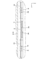
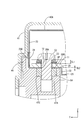
- FIG. AA cross section of FIG. The figure which expanded a part of FIG. BB cross section of FIG.
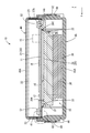
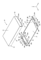
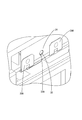
- Exploded perspective view of electrical junction box other than capacitor unit Perspective view showing the first shield case and the second shield case
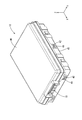
- the electric junction box 10 (FIG. 1) of the present embodiment is provided separately from a main power supply for supplying driving force of a vehicle in a vehicle such as an electric vehicle or a hybrid vehicle, and is used for a vehicle electric component or a motor of a device. It can be used as an auxiliary power source capable of supplying electric power.
- the X direction in FIG. 1 is the left side
- the Y direction is the front side
- the Z direction is the upper side.
- the electric junction box 10 includes a circuit board 11, a first shield case 20 arranged on the upper surface side (one surface side) of the circuit board 11, and a lower surface side (one side) of the circuit board 11. Second shield case 25 arranged on the opposite side), a capacitor unit 35 arranged below the second shield case 25, the circuit board 11, the first shield case 20, the second shield case 25, and the capacitor. A resin case 40, 45 made of synthetic resin in which the unit 35 is housed is provided.
- a printed circuit board in which a conductive path is formed on an insulating plate by a printed wiring technique is used, and as shown in FIG. 7, a plurality of terminal insertion holes 12 through which the lead terminals 36A are inserted and screws 52.
- a plurality of screw holes 13 through which the shaft portion is inserted and a plurality of positioning holes 14A and 14B for positioning the circuit board 11 are formed so as to penetrate therethrough.
- the plurality of screw holes 13 and the plurality of positioning holes 14A and 14B are provided in the peripheral portion of the circuit board 11 at intervals.
- a positioning pin 37A (positioning portion) of the capacitor unit 35 is inserted into the positioning hole 14A to relatively position the capacitor unit 35 and the circuit board 11.
- the positioning pin 14 (positioning portion) of the second resin case 45 is inserted into the positioning hole 14B to relatively position the second resin case 45 and the circuit board 11.
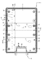
- a plurality of electronic components 15 to 17 are mounted on the conductive paths on both sides of the circuit board 11.
- the plurality of electronic components 15 to 17 are composed of FETs (Field effect transistors), resistors, diodes, coils, capacitors, microcomputers, etc., and their terminals are connected to the conductive paths of the circuit board 11.
- FETs Field effect transistors
- resistors diodes, coils, capacitors, microcomputers, etc.
- the electronic component 17 in which noise is hard to occur is mounted.
- the shield area A1 on the lower surface side of the circuit board 11 is mounted with an electronic component 16 that is shorter (smaller in height in the vertical direction) than the shield area A1 on the upper surface side of the circuit board 11.
- Examples of the short electronic component 16 include resistors, diodes, short capacitors, and the like.
- the circuit board 11 is not limited to the printed circuit board, and may be formed by stacking a bus bar made of a metal plate material such as copper or copper alloy on the printed circuit board.
- a connector 18 is fixed to the front end of the circuit board 11.
- the connector 18 includes a housing 18A having a hood-like opening and a connector terminal 18B fixed to the housing 18A.
- the connector terminal 18B is connected to the conductive path of the circuit board 11 by being soldered to the land portion of the circuit board 11.
- the first shield case 20 is made of a metal such as iron, stainless steel, or aluminum, has a size that covers the shield area A1 on the upper surface of the circuit board 11, and has a rectangular top plate portion 21 as shown in FIG. Side wall portions 22 and 22 extending downward from both end portions of the top plate portion 21 and end wall portions 23 and 23 extending downward from front and rear end portions of the top plate portion 21 are provided.
- the end wall portions 23, 23 extend longer than the side wall portions 22, 22, and a clearance CL1 is formed between the side wall portions 22, 22 and the upper surface of the circuit board 11, as shown in FIG. It
- the lower end side (tip end side) of the end wall portions 23, 23 is a locked portion 24, and as shown in FIG. 8, a circular locked hole 24A formed through the locked portion 24. Are lined up on the left and right.
- the second shield case 25 is made of a metal such as iron, stainless steel, or aluminum, and has a rectangular facing portion 26 facing the lower surface of the circuit board 11 with a space therebetween, and both side edge portions of the facing portion 26. , A pair of side wall portions 27, 27 extending upward from the front and rear portions, and a stacking portion 28 extending in the front-rear direction with respect to the facing portion 26 via a step portion 32 having a step-like shape and being stacked in close contact with the circuit board 11. 28, and a plurality of locking pieces 29A, 29B provided at the tip of the overlapping portions 28, 28 and standing upright (in a direction intersecting the plate surfaces of the overlapping portions 28, 28).
- a plurality of through holes 26 ⁇ /b>A through which the terminals can be inserted are formed side by side on the one overlapping portion 28 side of the facing portion 26.
- the side wall portions 27, 27 are smaller in height than the step portion 32. As shown in FIG. 6, when the second shield case 25 is attached to the circuit board 11, the side wall portions 27, 27 have a height dimension smaller than that of the step portion 32.
- a clearance CL2 is formed between the upper end (tip) and the lower surface of the circuit board 11.
- the overlapping portions 28, 28 are overlapped with the front end portion and the rear end portion in the middle portion of the circuit board 11 in the left-right direction, and include a fastening portion 28B that is screwed with a screw 52.
- the fastening portion 28B is formed with a plurality of screw holes 28A through which the shaft portion of the screw 52 is inserted.
- the overlapping portion 28 is provided with a relief recess 28C for escaping the head portion of the screw 52 when the capacitor unit 35 is screwed.
- the ground pattern GP is formed.
- the formed circuit board 11 and the fastening portion 28B are sandwiched between the head of the screw 52 and the nut 54.
- the second shield case 25 is connected to the ground potential via the ground pattern GP.
- the plurality of locking pieces 29A and 29B are provided with locking pieces 29A and locking pieces 29B alternately in the left-right direction, and the positions of the locking pieces 29A in the front-rear direction and the locking pieces 29B.
- a gap is formed between the position and the position of, and has a row of a plurality of first locking pieces 29A and a row of a plurality of second locking pieces 29B.
- the locked portion 24 of the first shield case 20 can be held between the row of the plurality of first locking pieces 29A and the row of the plurality of second locking pieces 29B.
- Each of the first locking piece 29A and the second locking piece 29B has a protrusion 30 that protrudes toward the locked portion 24 (inward of each other).
- a recess corresponding to the shape of the protrusion 30 is formed on the surface of the locking pieces 29A, 29B opposite to the protrusion 30.
- the second shield case 25 and the second shield case 25 are held in the assembled state.
- the locked portion 24 is in contact with the first locking piece 29A and the second locking piece 29B, so that the first shield case 20 is grounded via the second shield case 25.
- the protrusion 30 is fitted into the locked hole 24A while being electrically connected to the electric potential, so that the detachment of the first shield case 20 and the second shield case 25 is restricted.
- the first shield case 20 and the second shield case 25 can be formed by punching a thin metal plate material into a developed shape by a pressing machine and then performing bending work.
- the protrusion 30 can be formed, for example, when the metal plate material is punched out by a pressing machine.
- the capacitor unit 35 includes a plurality of capacitors 36 such as electric double layer capacitors and lithium ion capacitors, and a synthetic resin capacitor holder 37 that holds the plurality of capacitors 36 side by side.
- the capacitor 36 has, for example, a cylindrical shape and has a pair of positive and negative lead terminals 36A.
- the capacitor holder 37 includes a plurality of concave portions (not shown) into which the plurality of capacitors 36 are fitted in a lined state, and is covered with a capacitor cover 38 that restricts the separation of the plurality of capacitors 36.
- the capacitor holder 37 is provided with a positioning pin 37A that enters the escape recess 28C of the second shield case 25 and is inserted into the positioning hole 14A to position the relative positions of the circuit board 11 and the capacitor unit 35.
- the resin cases 40 and 45 include a first resin case 40 and a second resin case 45 that fits into the first resin case 40, as shown in FIG. 7.
- the first resin case 40 has a box shape with an open lower side, and includes a rectangular tubular peripheral wall portion 41 extending downward from a peripheral edge of a rectangular plate-shaped ceiling wall 40A. At the lower end of the peripheral wall portion 41, a plurality of flexurally deformable frame-shaped locking frames 42 are provided at intervals over the entire circumference.
- the peripheral wall portion 41 of the first resin case 40 has a lead-out recess 43 in which the connector 18 is led out.
- the second resin case 45 includes a rectangular plate-shaped bottom wall 45A and an upright wall 46 in the shape of a rectangular tube that is erected upward from the peripheral edge of the bottom wall 45A over the entire circumference.
- a plurality of boss portions 47A and 47B and a positioning pin 48 are provided inside the standing wall 46.
- the plurality of boss portions 47A, 47B and the positioning pin 48 are provided at intervals in the circumferential direction, and are formed at positions adjacent to the standing wall 46.
- a recess 47C that accommodates the nut 54 while the rotation of the nut 54 is restricted and a recess 47D that allows the shaft of the screw 52 to escape are formed in the upper portion of the plurality of bosses 47A and 47B.
- the positioning pin 48 has a rod shape and is inserted into the positioning holes 14A and 14B of the circuit board 11 to position the circuit board 11.
- a locking projection 49 that locks the locking frame 42 and restricts the separation of the first resin case 40 is formed.
- the overlapping portions 28, 28 of the second shield case 25 are mounted on the plurality of boss portions 47A. Place.
- the circuit board 11 on which the connector 18 is mounted and the plurality of electronic components 15 to 17 are mounted is placed on the second shield case 25 so that the positioning pins 37A and 48 pass through the positioning holes 14A and 14B (FIG. 7). reference).
- the shaft portion of the screw 52 is passed through the screw hole 13 and the screw hole 28A, and the circuit board 11 and the overlapping portions 28, 28 are fastened to the plurality of boss portions 47A with the screw 52.
- the circuit board 11 is fixed to the second resin case 45 by fastening the boss portion 47B and the like with the screw 52.
- the locked portion 24 of the first shield case 20 becomes the first locking piece 29A of the second shield case 25.
- the protrusion 30 of the first locking piece 29A and the second locking piece 29B is sandwiched between the second locking piece 29B and the second locking piece 29B, and is fitted into the locked hole 24A.
- the locked portion 24 is locked between the first locking piece 29A and the second locking piece 29B, and the shield cases 20 and 25 are connected to the ground potential.
- the electrical junction box 10 has a circuit board 11 on which electronic components 15 to 17 are mounted, a conductive first shield case 20 that covers one surface of the circuit board 11, and a circuit board 11 among the circuit board 11.
- a conductive second shield case 25 covering the side opposite to the one surface side, a resin first resin case 40 covering the first shield case 20, and a resin second resin case 45 covering the second shield case 25.
- both surface sides of the circuit board 11 are covered with the first shield case 20 and the second shield case 25, and the outer sides of the first shield case 20 and the second shield case 25 are covered with the resin cases 40 and 45.
- the shield function can be generated in the shield areas A1 on both sides of the circuit board 11, and the weight of the electrical junction box 10 can be reduced as compared with the configuration in which the exterior of the electrical junction box 10 is a metal case. It will be possible. Further, as compared with a configuration in which a metal casing is used as the exterior of the electrical junction box 10, it is possible to use a thin metal plate material for the shield cases 20 and 25, so that the shield cases 20 and 25 can be easily formed. Therefore, the manufacturing cost can be reduced.
- the electronic components 15 to 17 are plural, and are provided with a FET or the like (high noise component) and a coil or the like (low noise component) having less noise than the FET or the like, and the first shield case 20 and the second shield case.
- At least one of the areas 25 is smaller than the entire area of the circuit board 11 and covers the plate surface of the circuit board 11 so as to include the shield area A1 on which the FET and the like are mounted. This makes it possible to further reduce the weight and manufacturing cost of the electrical junction box 10 as compared with the configuration in which the entire area of the circuit board 11 is covered with the shield case.
- the first shield case 20 (and one of the second shield cases 25) includes a plate-shaped locked portion 24, and the second shield case 25 (and the other of the first shield case 20) is locked.
- a first locking piece 29A and a second locking piece 29B sandwiching the portion 24 are provided, and the first locking piece 29A and the second locking piece 29B are provided side by side along the locked portion 24. .
- the conductive path includes a ground pattern GP connected to the ground potential, and the second shield case 25 (and at least one of the first shield case 20) is screwed to the circuit board 11 and connected to the ground pattern GP. And a retaining portion 28B.
- the shield cases 20 and 25 can be connected to the ground potential by using the configuration for fixing the second shield case 25 (and at least one of the first shield case 20) to the circuit board 11. .
- the second shield case 25 (and at least one of the first shield case 20) includes a retaining portion 28B and a facing portion 26 that faces the circuit board 11 with a space therebetween.
- a step 32 is formed between the step 26 and the step 26. With this configuration, the step portion 32 can form a space between the circuit board 11 and the facing portion 26 in which the electronic component 16 is housed.
- first shield case 20 and the second shield case 25 includes a side wall portion 22 (27) having a plate surface in a direction intersecting the plate surface of the circuit board 11, and the side wall portion 22 ( In the end portion 27) on the circuit board 11 side, clearances CL1 and CL2 are formed with the surface of the circuit board 11. By doing so, it is possible to suppress a short circuit due to the contact between the conductive path having a potential higher than the glide potential on the upper surface and the lower surface of the circuit board 11 and the tip of the side wall portion 22 (27) in the shield cases 20 and 25. ..
- a capacitor 36 is housed between the second shield case 25 and the second resin case 45. With this configuration, the second shield case 25 and the electronic component 16 can be arranged in the gap between the circuit board 11 and the capacitor 36.
- the electronic component 16 is mounted on the back surface of the circuit board 11 (the shield area A1 covered by the second shield case 25), but the invention is not limited to this.
- the shield area A1 on the back surface of the circuit board 11 is not limited to this. It is also possible to adopt a configuration in which only the conductive path is arranged without mounting the electronic component on the.
- the range of the shield area A1 of the circuit board 11 covered by the first shield case 20 and the second shield case 25 is not limited to the configuration of the above embodiment.
- one or both of the first shield case 20 and the second shield case 25 may cover the entire circuit board 11.
- the locked hole 24A of the first shield case 20 is a through hole, but is not limited to this, and the protrusion 30 may be locked in a locking recess that does not penetrate.
- the locked hole 24A is provided in the first shield case 20 and the locking pieces 29A and 29B are provided in the second shield case 25, the invention is not limited to this, and the locking piece is provided in the first shield case 20.
- the second shield case 25 may be provided with a locked hole for locking the locking piece.
- the second shield case 25 is provided with the retaining portion 28B connected to the ground potential
- the invention is not limited to this, and the first shield case 20 may be provided with the retaining portion connected to the ground potential.
- the step portion 32 is provided on the second shield case 25, the step portion may be provided on the first shield case 20.
Abstract
This electrical junction box 10 comprises: a circuit board 11 having an electroconductive path, electronic components 15-17 being mounted on the circuit board 11; an electroconductive first shield case 20 that covers one surface side of the circuit board 11; an electroconductive second shield case 25 that covers the side of the circuit board 11 opposite the one surface side; a first resin case 40 made of resin, the first resin case 40 covering the first shield case 20; and a second resin case 45 made of resin, the second resin case 45 covering the second shield case 25.
Description
本明細書では、電気接続箱に関する技術を開示する。
In this specification, the technology related to the electrical junction box is disclosed.
従来、回路基板がケースに収容された電気接続箱が知られている。特許文献1の電気接続箱は、リレー等の電子部品が実装された回路基板と、回路基板の下に重ねられる金属製の放熱部材と、回路基板が重ねられた放熱部材の上方側を覆う金属製のケースとを備えている。電気接続箱のケースと放熱部材とが回路基板を覆うことにより、電気接続箱にシールド機能を生じさせている。
Conventionally, an electric junction box in which a circuit board is housed in a case is known. The electric junction box of Patent Document 1 includes a circuit board on which electronic components such as a relay are mounted, a metal heat dissipation member stacked under the circuit board, and a metal covering an upper side of the heat dissipation member on which the circuit board is stacked. It is equipped with a case. By covering the circuit board with the case of the electric connection box and the heat dissipation member, the electric connection box has a shielding function.
ところで、電気接続箱にシールド機能を生じさせるために、電気接続箱の外装を金属製のケースとすると、金属の重量により電気接続箱の軽量化の障害となるとともに、合成樹脂製のケースと比較して製造時の金型の耐久性が低いため、製造コストが高くなりやすいという問題がある。
By the way, if a metal case is used as the exterior of the electric junction box in order to create a shielding function for the electric junction box, the weight of the metal will hinder the weight reduction of the electric junction box, and compared with the case made of synthetic resin. Then, since the durability of the mold during manufacturing is low, there is a problem that the manufacturing cost tends to increase.
本明細書に記載された技術は、上記のような事情に基づいて完成されたものであって、電気接続箱を軽量化しつつ製造コストを低減することを目的とする。
The technology described in this specification has been completed based on the above circumstances, and its purpose is to reduce the manufacturing cost while reducing the weight of the electrical junction box.
本明細書に記載された電気接続箱は、導電路を有し、電子部品が実装される回路基板と、前記回路基板の一面側を覆う導電性の第1シールドケースと、前記回路基板のうち、前記一面側とは反対側を覆う導電性の第2シールドケースと、前記第1シールドケースを覆う樹脂製の第1樹脂ケースと、前記第2シールドケースを覆う樹脂製の第2樹脂ケースと、を備える。
上記構成によれば、回路基板の両面側が第1シールドケース及び第2シールドケースで覆われ、第1シールドケース及び第2シールドケースの外側が樹脂ケースにより覆われるため、回路基板の両面に対してシールド機能を生じさせつつ、電気接続箱の外装を金属ケースとする構成と比較して、電気接続箱の軽量化が可能になる。また、電気接続箱の外装にシールドケースを用いる構成と比較してシールドケースに薄肉の金属板材を使うことが可能になるため、シールドケースの成形が容易になり、製造コストの低減が可能になる。 The electrical junction box described in this specification has a circuit board on which an electronic component is mounted, a conductive first shield case that covers one surface side of the circuit board, and A conductive second shield case covering the side opposite to the one surface side, a resin first resin case covering the first shield case, and a resin second resin case covering the second shield case. , Is provided.
According to the above configuration, both sides of the circuit board are covered with the first shield case and the second shield case, and the outer sides of the first shield case and the second shield case are covered with the resin case. It is possible to reduce the weight of the electrical junction box as compared with the configuration in which the exterior of the electrical junction box is a metal case while generating the shield function. Further, as compared to a configuration in which a shield case is used as the exterior of the electrical junction box, it is possible to use a thin metal plate material for the shield case, so that the shield case can be easily molded and the manufacturing cost can be reduced. ..
本明細書に記載された技術の実施態様としては以下の態様が好ましい。
前記電子部品は、複数であり、高ノイズ部品と、前記高ノイズ部品よりもノイズの小さい低ノイズ部品とを備え、前記第1シールドケース及び前記第2シールドケースの少なくとも一方は、前記回路基板の全体の領域よりも小さい領域で、前記高ノイズ部品が実装された領域を含むように前記回路基板の面を覆っている。 The following aspects are preferable as the embodiments of the technology described in the present specification.
The electronic components are plural and include a high-noise component and a low-noise component whose noise is smaller than that of the high-noise component, and at least one of the first shield case and the second shield case is provided on the circuit board. An area smaller than the entire area covers the surface of the circuit board so as to include an area in which the high noise component is mounted.
前記第1シールドケース及び前記第2シールドケースの一方は、板状の被係止部を備え、前記第1シールドケース及び前記第2シールドケースの他方は、前記被係止部を挟む第1係止片と第2係止片とを備え、前記第1係止片と前記第2係止片とは前記被係止部に沿って並んで設けられている。
One of the first shield case and the second shield case includes a plate-shaped locked portion, and the other of the first shield case and the second shield case is a first member that sandwiches the locked portion. A stop piece and a second engagement piece are provided, and the first engagement piece and the second engagement piece are provided side by side along the engaged portion.
前記導電路は、グランド電位に接続されたグランドパターンを備え、前記第1シールドケース及び前記第2シールドケースの少なくとも一方は、前記回路基板にネジ留めされて前記グランドパターンに接続される留め部を備える。
The conductive path includes a ground pattern connected to a ground potential, and at least one of the first shield case and the second shield case has a fastening portion screwed to the circuit board and connected to the ground pattern. Prepare
前記第1シールドケース及び前記第2シールドケースの少なくとも一方は、前記留め部と、前記回路基板に対して間隔を空けて対向する対向部とを備え、前記留め部と前記対向部との間には、段差部が形成されている。
At least one of the first shield case and the second shield case includes the retaining portion and a facing portion that faces the circuit board with a gap, and is disposed between the retaining portion and the facing portion. Has a stepped portion.
前記第1シールドケース及び前記第2シールドケースの少なくとも一方は、前記回路基板の板面に対して交差する方向の板面を有する側壁部を備え、前記側壁部における前記回路基板側の端部は、前記回路基板の面との間にクリアランスが形成されている。
At least one of the first shield case and the second shield case includes a side wall portion having a plate surface in a direction intersecting with the plate surface of the circuit board, and an end portion of the side wall portion on the circuit board side is provided. A clearance is formed between the circuit board and the surface of the circuit board.
前記第2シールドケースと、前記第2樹脂ケースとの間には、キャパシタが収容されている。
A capacitor is housed between the second shield case and the second resin case.
本明細書に記載された技術によれば、電気接続箱を軽量化しつつ製造コストを低減することが可能になる。
According to the technology described in this specification, it is possible to reduce the manufacturing cost while reducing the weight of the electrical junction box.
実施形態1について図1~図9を参照しつつ説明する。
本実施形態の電気接続箱10(図1)は、例えば、電気自動車やハイブリッド自動車等の車両において、車両の駆動力を供給する主電源とは別に設けられ、車載電装品や機器のモータ等へ電力を供給可能な補助電源として使用することができる。以下では、図1のX方向を左方、Y方向を前方、Z方向を上方として説明する。 The first embodiment will be described with reference to FIGS. 1 to 9.
The electric junction box 10 (FIG. 1) of the present embodiment is provided separately from a main power supply for supplying driving force of a vehicle in a vehicle such as an electric vehicle or a hybrid vehicle, and is used for a vehicle electric component or a motor of a device. It can be used as an auxiliary power source capable of supplying electric power. In the following description, the X direction in FIG. 1 is the left side, the Y direction is the front side, and the Z direction is the upper side.
電気接続箱10は、図4に示すように、回路基板11と、回路基板11の上面側(一方の面側)に配される第1シールドケース20と、回路基板11の下面側(一方側とは反対側)に配される第2シールドケース25と、第2シールドケース25の下側に配されるキャパシタユニット35と、回路基板11、第1シールドケース20、第2シールドケース25及びキャパシタユニット35が収容される合成樹脂製の樹脂ケース40,45と、を備える。
As shown in FIG. 4, the electric junction box 10 includes a circuit board 11, a first shield case 20 arranged on the upper surface side (one surface side) of the circuit board 11, and a lower surface side (one side) of the circuit board 11. Second shield case 25 arranged on the opposite side), a capacitor unit 35 arranged below the second shield case 25, the circuit board 11, the first shield case 20, the second shield case 25, and the capacitor. A resin case 40, 45 made of synthetic resin in which the unit 35 is housed is provided.
回路基板11は、プリント配線技術により絶縁板に導電路が形成されたプリント基板が用いられており、図7に示すように、リード端子36Aが挿通される複数の端子挿通孔12と、ネジ52の軸部が挿通される複数のネジ孔13と、回路基板11を位置決めする複数の位置決め孔14A,14Bとが貫通形成されている。複数のネジ孔13及び複数の位置決め孔14A,14Bは、回路基板11の周縁部に間隔を空けて設けられている。位置決め孔14Aは、キャパシタユニット35の位置決めピン37A(位置決め部)が挿通され、キャパシタユニット35と回路基板11とを相対的に位置決めする。位置決め孔14Bは、第2樹脂ケース45の位置決めピン48(位置決め部)が挿通され、第2樹脂ケース45と回路基板11とを相対的に位置決めする。回路基板11の両面の導電路には、図2,図4に示すように、複数の電子部品15~17が実装されている。複数の電子部品15~17は、FET(Field effect transistor)、抵抗、ダイオード、コイル、コンデンサ、マイコン等から構成されており、それらの端子が回路基板11の導電路に接続されている。図2に示すように、回路基板11のうち、第1シールドケース20及び第2シールドケース25で覆われるシールド領域A1には、スイッチングによるノイズが発生しやすいFET等の電子部品15が実装され、シールド領域A1以外の非シールド領域A2,A3には、ノイズが発生しにくい電子部品17が実装される。回路基板11の下面側のシールド領域A1は、回路基板11の上面側のシールド領域A1と比較して、背の低い(上下方向の高さ寸法の小さい)電子部品16が実装されている。背の低い電子部品16としては、例えば、抵抗、ダイオード、背の低いコンデンサ等がある。なお、回路基板11は、プリント基板のみに限られず、例えば、プリント基板に銅、銅合金等の金属板材からなるバスバーを重ねて回路基板を構成してもよい。
As the circuit board 11, a printed circuit board in which a conductive path is formed on an insulating plate by a printed wiring technique is used, and as shown in FIG. 7, a plurality of terminal insertion holes 12 through which the lead terminals 36A are inserted and screws 52. A plurality of screw holes 13 through which the shaft portion is inserted and a plurality of positioning holes 14A and 14B for positioning the circuit board 11 are formed so as to penetrate therethrough. The plurality of screw holes 13 and the plurality of positioning holes 14A and 14B are provided in the peripheral portion of the circuit board 11 at intervals. A positioning pin 37A (positioning portion) of the capacitor unit 35 is inserted into the positioning hole 14A to relatively position the capacitor unit 35 and the circuit board 11. The positioning pin 14 (positioning portion) of the second resin case 45 is inserted into the positioning hole 14B to relatively position the second resin case 45 and the circuit board 11. As shown in FIGS. 2 and 4, a plurality of electronic components 15 to 17 are mounted on the conductive paths on both sides of the circuit board 11. The plurality of electronic components 15 to 17 are composed of FETs (Field effect transistors), resistors, diodes, coils, capacitors, microcomputers, etc., and their terminals are connected to the conductive paths of the circuit board 11. As shown in FIG. 2, in the circuit board 11, in the shield area A1 covered by the first shield case 20 and the second shield case 25, an electronic component 15 such as an FET that is apt to generate noise due to switching is mounted. In the non-shielded areas A2 and A3 other than the shielded area A1, the electronic component 17 in which noise is hard to occur is mounted. The shield area A1 on the lower surface side of the circuit board 11 is mounted with an electronic component 16 that is shorter (smaller in height in the vertical direction) than the shield area A1 on the upper surface side of the circuit board 11. Examples of the short electronic component 16 include resistors, diodes, short capacitors, and the like. The circuit board 11 is not limited to the printed circuit board, and may be formed by stacking a bus bar made of a metal plate material such as copper or copper alloy on the printed circuit board.
回路基板11の前端部には、コネクタ18が固定されている。コネクタ18は、フード状に開口するハウジング18Aと、ハウジング18Aに固定されるコネクタ端子18Bとを備える。コネクタ端子18Bは、回路基板11のランド部に半田付けされることにより、回路基板11の導電路に接続されている。
A connector 18 is fixed to the front end of the circuit board 11. The connector 18 includes a housing 18A having a hood-like opening and a connector terminal 18B fixed to the housing 18A. The connector terminal 18B is connected to the conductive path of the circuit board 11 by being soldered to the land portion of the circuit board 11.
第1シールドケース20は、鉄、ステンレス鋼、アルミニウム等の金属からなり、回路基板11の上面のシールド領域A1を覆う大きさとされ、図8に示すように、長方形状の天板部21と、天板部21の両側端部から下方に延びる側壁部22,22と、天板部21の前後の端部から下方に延びる端壁部23,23とを備える。端壁部23,23は、側壁部22,22よりも下方に長く延びており、図6に示すように、側壁部22,22と回路基板11の上面との間にはクリアランスCL1が形成される。端壁部23,23の下端部側(先端部側)は、被係止部24とされ、図8に示すように、被係止部24に貫通形成された円形状の被係止孔24Aが左右に並んでいる。
The first shield case 20 is made of a metal such as iron, stainless steel, or aluminum, has a size that covers the shield area A1 on the upper surface of the circuit board 11, and has a rectangular top plate portion 21 as shown in FIG. Side wall portions 22 and 22 extending downward from both end portions of the top plate portion 21 and end wall portions 23 and 23 extending downward from front and rear end portions of the top plate portion 21 are provided. The end wall portions 23, 23 extend longer than the side wall portions 22, 22, and a clearance CL1 is formed between the side wall portions 22, 22 and the upper surface of the circuit board 11, as shown in FIG. It The lower end side (tip end side) of the end wall portions 23, 23 is a locked portion 24, and as shown in FIG. 8, a circular locked hole 24A formed through the locked portion 24. Are lined up on the left and right.
第2シールドケース25は、鉄、ステンレス鋼、アルミニウム等の金属からなり、回路基板11の下面に対して間隔を空けて対向配置される長方形状の対向部26と、対向部26の両側縁部から上方に延びる一対の側壁部27,27と、対向部26に対して段差状の段差部32を介して前後方向に延出され、回路基板11に対して密着状態で重ねられる重ね部28,28と、重ね部28,28の先端部に設けられ、上方(重ね部28,28の板面と交差する方向)に起立した複数の係止片29A,29Bとを備える。対向部26における一方の重ね部28側には、端子を挿通可能な複数の貫通孔26Aが並んで形成されている。側壁部27,27は、段差部32よりも高さ寸法が小さくされており、図6に示すように、第2シールドケース25が回路基板11に取り付けられた状態では、側壁部27,27の上端(先端)と回路基板11の下面との間にはクリアランスCL2が形成される。
The second shield case 25 is made of a metal such as iron, stainless steel, or aluminum, and has a rectangular facing portion 26 facing the lower surface of the circuit board 11 with a space therebetween, and both side edge portions of the facing portion 26. , A pair of side wall portions 27, 27 extending upward from the front and rear portions, and a stacking portion 28 extending in the front-rear direction with respect to the facing portion 26 via a step portion 32 having a step-like shape and being stacked in close contact with the circuit board 11. 28, and a plurality of locking pieces 29A, 29B provided at the tip of the overlapping portions 28, 28 and standing upright (in a direction intersecting the plate surfaces of the overlapping portions 28, 28). A plurality of through holes 26</b>A through which the terminals can be inserted are formed side by side on the one overlapping portion 28 side of the facing portion 26. The side wall portions 27, 27 are smaller in height than the step portion 32. As shown in FIG. 6, when the second shield case 25 is attached to the circuit board 11, the side wall portions 27, 27 have a height dimension smaller than that of the step portion 32. A clearance CL2 is formed between the upper end (tip) and the lower surface of the circuit board 11.
重ね部28,28は、回路基板11の左右方向の中間部における前端部及び後端部に重ねられており、ネジ52でネジ留めされる留め部28Bを備える。留め部28Bは、ネジ52の軸部が挿通される複数のネジ孔28Aが貫通形成されている。一方の重ね部28には、図8に示すように、キャパシタユニット35のネジ留めの際のネジ52の頭部を逃がす逃がし凹部28Cが切り欠かれている。図6に示すように、ネジ52の軸部にワッシャー53を通した状態で回路基板11及び重ね部28,28のネジ孔13,28Aに通し、ナット54で締結することにより、グランドパターンGPが形成された回路基板11と、留め部28Bとがネジ52の頭部とナット54との間に挟持される。これにより、第2シールドケース25がグランドパターンGPを介してグランド電位に接続される。
The overlapping portions 28, 28 are overlapped with the front end portion and the rear end portion in the middle portion of the circuit board 11 in the left-right direction, and include a fastening portion 28B that is screwed with a screw 52. The fastening portion 28B is formed with a plurality of screw holes 28A through which the shaft portion of the screw 52 is inserted. As shown in FIG. 8, the overlapping portion 28 is provided with a relief recess 28C for escaping the head portion of the screw 52 when the capacitor unit 35 is screwed. As shown in FIG. 6, by passing the washer 53 through the shaft portion of the screw 52 through the screw holes 13 and 28A of the circuit board 11 and the overlapping portions 28 and 28, and fastening with the nut 54, the ground pattern GP is formed. The formed circuit board 11 and the fastening portion 28B are sandwiched between the head of the screw 52 and the nut 54. As a result, the second shield case 25 is connected to the ground potential via the ground pattern GP.
複数の係止片29A,29Bは、図8に示すように、係止片29Aと係止片29Bとが左右方向に交互に設けられ、前後方向における係止片29Aの位置と係止片29Bの位置との間には隙間が形成されており、複数の第1係止片29Aの列と、複数の第2係止片29Bの列とを有する。複数の第1係止片29Aの列と複数の第2係止片29Bの列との間には、第1シールドケース20の被係止部24を挟持可能とされている。第1係止片29Aと第2係止片29Bとは、共に、被係止部24側(互いの内方側)に突出する突部30を有する。係止片29A,29Bにおける突部30とは反対側の面には、突部30の形状に応じた凹みが形成されている。第1係止片29Aと第2係止片29Bとの間の隙間に第1シールドケース20の端壁部23,23が挿通されると、端壁部23,23に突部30が当接し、第1係止片29Aと第2係止片29Bとをわずかに弾性変形させつつ、第1係止片29Aと第2係止片29Bとの間に被係止部24が差し込まれる。また、被係止部24の複数の被係止孔24Aに各突部30が嵌合することにより第1係止片29Aと第2係止片29Bとが弾性復元し、第1シールドケース20と第2シールドケース25とが組み付けられた状態に保持される。この状態では、被係止部24は、第1係止片29A及び第2係止片29Bに対して接触した状態となるため、第1シールドケース20は、第2シールドケース25を介してグランド電位に電気的に接続されるとともに、被係止孔24Aに各突部30が嵌合することにより、第1シールドケース20と第2シールドケース25との離脱が規制される。第1シールドケース20及び第2シールドケース25は、薄肉の金属板材をプレス機により展開形状に打ち抜き、その後、曲げ加工を施すことにより形成することができる。なお、突部30は、例えば、プレス機により金属板材を打ち抜いた際に形成することができる。
As shown in FIG. 8, the plurality of locking pieces 29A and 29B are provided with locking pieces 29A and locking pieces 29B alternately in the left-right direction, and the positions of the locking pieces 29A in the front-rear direction and the locking pieces 29B. A gap is formed between the position and the position of, and has a row of a plurality of first locking pieces 29A and a row of a plurality of second locking pieces 29B. The locked portion 24 of the first shield case 20 can be held between the row of the plurality of first locking pieces 29A and the row of the plurality of second locking pieces 29B. Each of the first locking piece 29A and the second locking piece 29B has a protrusion 30 that protrudes toward the locked portion 24 (inward of each other). A recess corresponding to the shape of the protrusion 30 is formed on the surface of the locking pieces 29A, 29B opposite to the protrusion 30. When the end wall portions 23, 23 of the first shield case 20 are inserted into the gap between the first locking piece 29A and the second locking piece 29B, the projection 30 comes into contact with the end wall portions 23, 23. The locked portion 24 is inserted between the first locking piece 29A and the second locking piece 29B while slightly elastically deforming the first locking piece 29A and the second locking piece 29B. Further, by fitting the protrusions 30 into the plurality of locked holes 24A of the locked portion 24, the first locking piece 29A and the second locking piece 29B are elastically restored, and the first shield case 20. The second shield case 25 and the second shield case 25 are held in the assembled state. In this state, the locked portion 24 is in contact with the first locking piece 29A and the second locking piece 29B, so that the first shield case 20 is grounded via the second shield case 25. The protrusion 30 is fitted into the locked hole 24A while being electrically connected to the electric potential, so that the detachment of the first shield case 20 and the second shield case 25 is restricted. The first shield case 20 and the second shield case 25 can be formed by punching a thin metal plate material into a developed shape by a pressing machine and then performing bending work. The protrusion 30 can be formed, for example, when the metal plate material is punched out by a pressing machine.
キャパシタユニット35は、図4に示すように、例えば電気二重層キャパシタ、リチウムイオンキャパシタ等の複数のキャパシタ36と、複数のキャパシタ36を並べて保持する合成樹脂製のキャパシタホルダ37とを備える。キャパシタ36は、例えば円柱状とされ、正負一対のリード端子36Aを有する。キャパシタホルダ37は、複数のキャパシタ36が並べられた状態で嵌合する複数の凹状部(不図示)を備え、複数のキャパシタ36の離脱を規制するキャパシタカバー38で覆われている。キャパシタホルダ37には、第2シールドケース25の逃げ凹部28Cに進入し、位置決め孔14Aに挿通されて回路基板11とキャパシタユニット35との相対的位置を位置決めする位置決めピン37Aが設けられている。
As shown in FIG. 4, the capacitor unit 35 includes a plurality of capacitors 36 such as electric double layer capacitors and lithium ion capacitors, and a synthetic resin capacitor holder 37 that holds the plurality of capacitors 36 side by side. The capacitor 36 has, for example, a cylindrical shape and has a pair of positive and negative lead terminals 36A. The capacitor holder 37 includes a plurality of concave portions (not shown) into which the plurality of capacitors 36 are fitted in a lined state, and is covered with a capacitor cover 38 that restricts the separation of the plurality of capacitors 36. The capacitor holder 37 is provided with a positioning pin 37A that enters the escape recess 28C of the second shield case 25 and is inserted into the positioning hole 14A to position the relative positions of the circuit board 11 and the capacitor unit 35.
樹脂ケース40,45は、図7に示すように、第1樹脂ケース40と、第1樹脂ケース40に嵌合する第2樹脂ケース45とを備える。第1樹脂ケース40は、下方側が開放された箱形であって、長方形の板状の天井壁40Aの周縁から下方に延びる角筒状の周壁部41を備える。周壁部41の下端部には、撓み変形可能な複数の枠状の係止枠42が全周に亘って間隔を空けて設けられている。第1樹脂ケース40の周壁部41には、コネクタ18が導出される導出凹部43が切り欠かれている。
The resin cases 40 and 45 include a first resin case 40 and a second resin case 45 that fits into the first resin case 40, as shown in FIG. 7. The first resin case 40 has a box shape with an open lower side, and includes a rectangular tubular peripheral wall portion 41 extending downward from a peripheral edge of a rectangular plate-shaped ceiling wall 40A. At the lower end of the peripheral wall portion 41, a plurality of flexurally deformable frame-shaped locking frames 42 are provided at intervals over the entire circumference. The peripheral wall portion 41 of the first resin case 40 has a lead-out recess 43 in which the connector 18 is led out.
第2樹脂ケース45は、長方形の板状の底壁45Aと、底壁45Aの周縁から全周に亘って上方側に起立する角筒状の起立壁46とを備える。起立壁46の内側には、複数のボス部47A,47Bと、位置決めピン48とが設けられている。複数のボス部47A,47B及び位置決めピン48は、周方向に間隔を空けて設けられ、起立壁46に隣接する位置に形成されている。複数のボス部47A,47Bの上部には、ナット54の回転を規制した状態でナット54を収容する凹部47Cと、ネジ52の軸部を逃がす逃がし凹部47Dとが形成されている。位置決めピン48は、棒状であって、回路基板11の位置決め孔14A,14Bに挿通されて回路基板11を位置決めする。第2樹脂ケース45の起立壁46の外周には、係止枠42を係止して、第1樹脂ケース40の離脱を規制する係止凸部49が形成されている。
The second resin case 45 includes a rectangular plate-shaped bottom wall 45A and an upright wall 46 in the shape of a rectangular tube that is erected upward from the peripheral edge of the bottom wall 45A over the entire circumference. Inside the standing wall 46, a plurality of boss portions 47A and 47B and a positioning pin 48 are provided. The plurality of boss portions 47A, 47B and the positioning pin 48 are provided at intervals in the circumferential direction, and are formed at positions adjacent to the standing wall 46. A recess 47C that accommodates the nut 54 while the rotation of the nut 54 is restricted and a recess 47D that allows the shaft of the screw 52 to escape are formed in the upper portion of the plurality of bosses 47A and 47B. The positioning pin 48 has a rod shape and is inserted into the positioning holes 14A and 14B of the circuit board 11 to position the circuit board 11. On the outer periphery of the standing wall 46 of the second resin case 45, a locking projection 49 that locks the locking frame 42 and restricts the separation of the first resin case 40 is formed.
電気接続箱10の組み付けについて説明する。
第2樹脂ケース45にキャパシタユニット35を収容し、第2樹脂ケース45の各凹部47Cにナット54を収容した状態で、第2シールドケース25の重ね部28,28を複数のボス部47Aに載置する。次に、コネクタ18が装着され、複数の電子部品15~17が実装された回路基板11を、位置決めピン37A,48が位置決め孔14A,14Bを通るように第2シールドケース25に重ねる(図7参照)。そして、ネジ52の軸部をネジ孔13,ネジ孔28Aに通して回路基板11及び重ね部28,28を複数のボス部47Aにネジ52で締結する。また、ボス部47B等についてもネジ52で締結し、回路基板11を第2樹脂ケース45に固定する。 Assembly of theelectrical junction box 10 will be described.
With thecapacitor unit 35 accommodated in the second resin case 45 and the nut 54 accommodated in each recess 47C of the second resin case 45, the overlapping portions 28, 28 of the second shield case 25 are mounted on the plurality of boss portions 47A. Place. Next, the circuit board 11 on which the connector 18 is mounted and the plurality of electronic components 15 to 17 are mounted is placed on the second shield case 25 so that the positioning pins 37A and 48 pass through the positioning holes 14A and 14B (FIG. 7). reference). Then, the shaft portion of the screw 52 is passed through the screw hole 13 and the screw hole 28A, and the circuit board 11 and the overlapping portions 28, 28 are fastened to the plurality of boss portions 47A with the screw 52. The circuit board 11 is fixed to the second resin case 45 by fastening the boss portion 47B and the like with the screw 52.
第2樹脂ケース45にキャパシタユニット35を収容し、第2樹脂ケース45の各凹部47Cにナット54を収容した状態で、第2シールドケース25の重ね部28,28を複数のボス部47Aに載置する。次に、コネクタ18が装着され、複数の電子部品15~17が実装された回路基板11を、位置決めピン37A,48が位置決め孔14A,14Bを通るように第2シールドケース25に重ねる(図7参照)。そして、ネジ52の軸部をネジ孔13,ネジ孔28Aに通して回路基板11及び重ね部28,28を複数のボス部47Aにネジ52で締結する。また、ボス部47B等についてもネジ52で締結し、回路基板11を第2樹脂ケース45に固定する。 Assembly of the
With the
次に、回路基板11の上側から第1シールドケース20を第2シールドケース25に嵌め合わせると、第1シールドケース20の被係止部24が第2シールドケース25における第1係止片29Aと第2係止片29Bとの間に挟まれ、第1係止片29A及び第2係止片29Bの突部30が被係止孔24Aに嵌合する。これにより、被係止部24が第1係止片29Aと第2係止片29Bとの間に係止された状態となり、シールドケース20,25がグランド電位に接続された状態となる。そして、第2樹脂ケース45に第1樹脂ケース40を被せ、第1樹脂ケース40の係止枠42の孔縁を第2樹脂ケース45の係止凸部49に係止させることにより、電気接続箱10が形成される(図1)。
Next, when the first shield case 20 is fitted to the second shield case 25 from the upper side of the circuit board 11, the locked portion 24 of the first shield case 20 becomes the first locking piece 29A of the second shield case 25. The protrusion 30 of the first locking piece 29A and the second locking piece 29B is sandwiched between the second locking piece 29B and the second locking piece 29B, and is fitted into the locked hole 24A. As a result, the locked portion 24 is locked between the first locking piece 29A and the second locking piece 29B, and the shield cases 20 and 25 are connected to the ground potential. Then, the second resin case 45 is covered with the first resin case 40, and the hole edge of the locking frame 42 of the first resin case 40 is locked to the locking convex portion 49 of the second resin case 45, whereby electrical connection is achieved. A box 10 is formed (Fig. 1).
本実施形態によれば、以下の作用・効果を奏する。
電気接続箱10は、導電路を有し、電子部品15~17が実装される回路基板11と、回路基板11の一面側を覆う導電性の第1シールドケース20と、回路基板11のうち、一面側とは反対側を覆う導電性の第2シールドケース25と、第1シールドケース20を覆う樹脂製の第1樹脂ケース40と、第2シールドケース25を覆う樹脂製の第2樹脂ケース45と、を備える。
本実施形態によれば、回路基板11の両面側が第1シールドケース20及び第2シールドケース25で覆われ、第1シールドケース20及び第2シールドケース25の外側が樹脂ケース40,45により覆われるため、回路基板11の両面側のシールド領域A1に対してシールド機能を生じさせることができるとともに、電気接続箱10の外装を金属ケースとする構成と比較して、電気接続箱10の軽量化が可能になる。また、電気接続箱10の外装に金属製の筐体を用いる構成と比較してシールドケース20,25に薄肉の金属板材を使うことが可能になるため、シールドケース20,25の成形が容易になり、製造コストの低減が可能になる。 According to this embodiment, the following actions and effects are exhibited.
Theelectrical junction box 10 has a circuit board 11 on which electronic components 15 to 17 are mounted, a conductive first shield case 20 that covers one surface of the circuit board 11, and a circuit board 11 among the circuit board 11. A conductive second shield case 25 covering the side opposite to the one surface side, a resin first resin case 40 covering the first shield case 20, and a resin second resin case 45 covering the second shield case 25. And
According to this embodiment, both surface sides of thecircuit board 11 are covered with the first shield case 20 and the second shield case 25, and the outer sides of the first shield case 20 and the second shield case 25 are covered with the resin cases 40 and 45. Therefore, the shield function can be generated in the shield areas A1 on both sides of the circuit board 11, and the weight of the electrical junction box 10 can be reduced as compared with the configuration in which the exterior of the electrical junction box 10 is a metal case. It will be possible. Further, as compared with a configuration in which a metal casing is used as the exterior of the electrical junction box 10, it is possible to use a thin metal plate material for the shield cases 20 and 25, so that the shield cases 20 and 25 can be easily formed. Therefore, the manufacturing cost can be reduced.
電気接続箱10は、導電路を有し、電子部品15~17が実装される回路基板11と、回路基板11の一面側を覆う導電性の第1シールドケース20と、回路基板11のうち、一面側とは反対側を覆う導電性の第2シールドケース25と、第1シールドケース20を覆う樹脂製の第1樹脂ケース40と、第2シールドケース25を覆う樹脂製の第2樹脂ケース45と、を備える。
本実施形態によれば、回路基板11の両面側が第1シールドケース20及び第2シールドケース25で覆われ、第1シールドケース20及び第2シールドケース25の外側が樹脂ケース40,45により覆われるため、回路基板11の両面側のシールド領域A1に対してシールド機能を生じさせることができるとともに、電気接続箱10の外装を金属ケースとする構成と比較して、電気接続箱10の軽量化が可能になる。また、電気接続箱10の外装に金属製の筐体を用いる構成と比較してシールドケース20,25に薄肉の金属板材を使うことが可能になるため、シールドケース20,25の成形が容易になり、製造コストの低減が可能になる。 According to this embodiment, the following actions and effects are exhibited.
The
According to this embodiment, both surface sides of the
また、電子部品15~17は、複数であり、FET等(高ノイズ部品)と、FET等よりもノイズの小さいコイル等(低ノイズ部品)とを備え、第1シールドケース20及び第2シールドケース25の少なくとも一方は、回路基板11の全体の領域よりも小さい領域で、FET等が実装されたシールド領域A1を含むように回路基板11の板面を覆っている。
このようにすれば、回路基板11の全体の領域をシールドケースで覆う構成と比較して、より一層、電気接続箱10の軽量化や製造コストの低減が可能になる。 Further, theelectronic components 15 to 17 are plural, and are provided with a FET or the like (high noise component) and a coil or the like (low noise component) having less noise than the FET or the like, and the first shield case 20 and the second shield case. At least one of the areas 25 is smaller than the entire area of the circuit board 11 and covers the plate surface of the circuit board 11 so as to include the shield area A1 on which the FET and the like are mounted.
This makes it possible to further reduce the weight and manufacturing cost of theelectrical junction box 10 as compared with the configuration in which the entire area of the circuit board 11 is covered with the shield case.
このようにすれば、回路基板11の全体の領域をシールドケースで覆う構成と比較して、より一層、電気接続箱10の軽量化や製造コストの低減が可能になる。 Further, the
This makes it possible to further reduce the weight and manufacturing cost of the
また、第1シールドケース20(及び第2シールドケース25の一方)は、板状の被係止部24を備え、第2シールドケース25(及び第1シールドケース20の他方)は、被係止部24を挟む第1係止片29Aと第2係止片29Bとを備え、第1係止片29Aと第2係止片29Bとは被係止部24に沿って並んで設けられている。
このようにすれば、第1シールドケース20と第2シールドケース25との組付作業を簡素化しつつ、第1シールドケース20と第2シールドケース25とが嵌合した状態を保持することができる。 The first shield case 20 (and one of the second shield cases 25) includes a plate-shaped lockedportion 24, and the second shield case 25 (and the other of the first shield case 20) is locked. A first locking piece 29A and a second locking piece 29B sandwiching the portion 24 are provided, and the first locking piece 29A and the second locking piece 29B are provided side by side along the locked portion 24. .
With this configuration, it is possible to maintain the fitted state of thefirst shield case 20 and the second shield case 25 while simplifying the assembling work of the first shield case 20 and the second shield case 25. .
このようにすれば、第1シールドケース20と第2シールドケース25との組付作業を簡素化しつつ、第1シールドケース20と第2シールドケース25とが嵌合した状態を保持することができる。 The first shield case 20 (and one of the second shield cases 25) includes a plate-shaped locked
With this configuration, it is possible to maintain the fitted state of the
また、導電路は、グランド電位に接続されたグランドパターンGPを備え、第2シールドケース25(及び第1シールドケース20の少なくとも一方)は、回路基板11にネジ留めされてグランドパターンGPに接続される留め部28Bを備える。
このようにすれば、第2シールドケース25(及び第1シールドケース20の少なくとも一方)を回路基板11に固定するための構成を利用してシールドケース20,25をグランド電位に接続することができる。 The conductive path includes a ground pattern GP connected to the ground potential, and the second shield case 25 (and at least one of the first shield case 20) is screwed to thecircuit board 11 and connected to the ground pattern GP. And a retaining portion 28B.
With this configuration, the shield cases 20 and 25 can be connected to the ground potential by using the configuration for fixing the second shield case 25 (and at least one of the first shield case 20) to the circuit board 11. .
このようにすれば、第2シールドケース25(及び第1シールドケース20の少なくとも一方)を回路基板11に固定するための構成を利用してシールドケース20,25をグランド電位に接続することができる。 The conductive path includes a ground pattern GP connected to the ground potential, and the second shield case 25 (and at least one of the first shield case 20) is screwed to the
With this configuration, the
また、第2シールドケース25(及び第1シールドケース20の少なくとも一方)は、留め部28Bと、回路基板11に対して間隔を空けて対向する対向部26とを備え、留め部28Bと対向部26との間には、段差部32が形成されている。
このようにすれば、段差部32により、回路基板11と対向部26との間に電子部品16が収容される空間を形成することができる。 The second shield case 25 (and at least one of the first shield case 20) includes a retainingportion 28B and a facing portion 26 that faces the circuit board 11 with a space therebetween. A step 32 is formed between the step 26 and the step 26.
With this configuration, thestep portion 32 can form a space between the circuit board 11 and the facing portion 26 in which the electronic component 16 is housed.
このようにすれば、段差部32により、回路基板11と対向部26との間に電子部品16が収容される空間を形成することができる。 The second shield case 25 (and at least one of the first shield case 20) includes a retaining
With this configuration, the
また、第1シールドケース20及び第2シールドケース25(の少なくとも一方)は、回路基板11の板面に対して交差する方向の板面を有する側壁部22(27)を備え、側壁部22(27)における回路基板11側の端部は、回路基板11の面との間にクリアランスCL1,CL2が形成されている。
このようにすれば、回路基板11の上面及び下面におけるグライド電位よりも高い電位の導電路とシールドケース20,25における側壁部22(27)の先端部との接触による短絡を抑制することができる。 Further, (at least one of) thefirst shield case 20 and the second shield case 25 includes a side wall portion 22 (27) having a plate surface in a direction intersecting the plate surface of the circuit board 11, and the side wall portion 22 ( In the end portion 27) on the circuit board 11 side, clearances CL1 and CL2 are formed with the surface of the circuit board 11.
By doing so, it is possible to suppress a short circuit due to the contact between the conductive path having a potential higher than the glide potential on the upper surface and the lower surface of thecircuit board 11 and the tip of the side wall portion 22 (27) in the shield cases 20 and 25. ..
このようにすれば、回路基板11の上面及び下面におけるグライド電位よりも高い電位の導電路とシールドケース20,25における側壁部22(27)の先端部との接触による短絡を抑制することができる。 Further, (at least one of) the
By doing so, it is possible to suppress a short circuit due to the contact between the conductive path having a potential higher than the glide potential on the upper surface and the lower surface of the
また、第2シールドケース25と、第2樹脂ケース45との間には、キャパシタ36が収容されている。
このようにすれば、回路基板11とキャパシタ36との間の隙間に第2シールドケース25及び電子部品16を配置することが可能になる。 Acapacitor 36 is housed between the second shield case 25 and the second resin case 45.
With this configuration, thesecond shield case 25 and the electronic component 16 can be arranged in the gap between the circuit board 11 and the capacitor 36.
このようにすれば、回路基板11とキャパシタ36との間の隙間に第2シールドケース25及び電子部品16を配置することが可能になる。 A
With this configuration, the
<他の実施形態>
本明細書に記載された技術は上記記述及び図面によって説明した実施形態に限定されるものではなく、例えば次のような実施形態も本明細書に記載された技術の技術的範囲に含まれる。 <Other Embodiments>
The technology described in this specification is not limited to the embodiments described by the above description and drawings, and the following embodiments are also included in the technical scope of the technology described in this specification.
(1)回路基板11の裏面(第2シールドケース25で覆われるシールド領域A1)には、電子部品16が実装される構成としたが、これに限られず、回路基板11の裏面のシールド領域A1に電子部品を実装せず、導電路のみが配されている構成としてもよい。
(1) The electronic component 16 is mounted on the back surface of the circuit board 11 (the shield area A1 covered by the second shield case 25), but the invention is not limited to this. The shield area A1 on the back surface of the circuit board 11 is not limited to this. It is also possible to adopt a configuration in which only the conductive path is arranged without mounting the electronic component on the.
(2)第1シールドケース20及び第2シールドケース25が覆う回路基板11のシールド領域A1の範囲は、上記実施形態の構成に限らない。例えば、第1シールドケース20及び第2シールドケース25の一方又は両方が回路基板11の全体を覆う構成としてもよい。
(2) The range of the shield area A1 of the circuit board 11 covered by the first shield case 20 and the second shield case 25 is not limited to the configuration of the above embodiment. For example, one or both of the first shield case 20 and the second shield case 25 may cover the entire circuit board 11.
(3)第1シールドケース20の被係止孔24Aは、貫通孔としたが、これに限られず、貫通していない係止凹部に突部30が係止される構成としてもよい。
(3) The locked hole 24A of the first shield case 20 is a through hole, but is not limited to this, and the protrusion 30 may be locked in a locking recess that does not penetrate.
(4)第1シールドケース20に被係止孔24Aを設け、第2シールドケース25に係止片29A,29Bを設けたが、これに限られず、第1シールドケース20に係止片を設け、第2シールドケース25に係止片に係止する被係止孔を設けてもよい。
(4) Although the locked hole 24A is provided in the first shield case 20 and the locking pieces 29A and 29B are provided in the second shield case 25, the invention is not limited to this, and the locking piece is provided in the first shield case 20. The second shield case 25 may be provided with a locked hole for locking the locking piece.
(5)第2シールドケース25にグランド電位に接続される留め部28Bを設けたが、これに限られず、第1シールドケース20にグランド電位に接続される留め部を設けてもよい。また、第2シールドケース25に段差部32を設けたが、第1シールドケース20に段差部を設けてもよい。
(5) Although the second shield case 25 is provided with the retaining portion 28B connected to the ground potential, the invention is not limited to this, and the first shield case 20 may be provided with the retaining portion connected to the ground potential. Further, although the step portion 32 is provided on the second shield case 25, the step portion may be provided on the first shield case 20.
10: 電気接続箱
11: 回路基板
15~17: 電子部品
20: 第1シールドケース
22,22: 側壁部
24: 被係止部
25: 第2シールドケース
26: 対向部
27,27: 側壁部
28B: 留め部
29A: 第1係止片
29B: 第2係止片
30: 突部
32: 段差部
36: キャパシタ
40: 第1樹脂ケース
45: 第2樹脂ケース
47A,47B: ボス部
52: ネジ
A1: シールド領域(領域)
GP: グランドパターン 10: Electric connection box 11:Circuit boards 15 to 17: Electronic component 20: First shield case 22, 22: Side wall part 24: Locked part 25: Second shield case 26: Opposing part 27, 27: Side wall part 28B : Fastening portion 29A: First locking piece 29B: Second locking piece 30: Projection 32: Step portion 36: Capacitor 40: First resin case 45: Second resin case 47A, 47B: Boss portion 52: Screw A1 : Shield area (area)
GP: Ground pattern
11: 回路基板
15~17: 電子部品
20: 第1シールドケース
22,22: 側壁部
24: 被係止部
25: 第2シールドケース
26: 対向部
27,27: 側壁部
28B: 留め部
29A: 第1係止片
29B: 第2係止片
30: 突部
32: 段差部
36: キャパシタ
40: 第1樹脂ケース
45: 第2樹脂ケース
47A,47B: ボス部
52: ネジ
A1: シールド領域(領域)
GP: グランドパターン 10: Electric connection box 11:
GP: Ground pattern
Claims (7)
- 導電路を有し、電子部品が実装される回路基板と、
前記回路基板の一面側を覆う導電性の第1シールドケースと、
前記回路基板のうち、前記一面側とは反対側を覆う導電性の第2シールドケースと、
前記第1シールドケースを覆う樹脂製の第1樹脂ケースと、
前記第2シールドケースを覆う樹脂製の第2樹脂ケースと、を備える電気接続箱。 A circuit board having a conductive path and on which electronic components are mounted,
A conductive first shield case covering one surface side of the circuit board;
A conductive second shield case covering the side of the circuit board opposite to the one surface side;
A first resin case made of resin that covers the first shield case;
An electrical junction box comprising: a second resin case made of resin, which covers the second shield case. - 前記電子部品は、複数であり、高ノイズ部品と、前記高ノイズ部品よりもノイズの小さい低ノイズ部品とを備え、前記第1シールドケース及び前記第2シールドケースの少なくとも一方は、前記回路基板の全体の領域よりも小さい領域で、前記高ノイズ部品が実装された領域を含むように前記回路基板の面を覆っている請求項1に記載の電気接続箱。 The electronic components are plural and include a high-noise component and a low-noise component whose noise is smaller than that of the high-noise component, and at least one of the first shield case and the second shield case is provided on the circuit board. The electrical junction box according to claim 1, wherein the surface of the circuit board is covered so as to include a region where the high-noise component is mounted in a region smaller than the entire region.
- 前記第1シールドケース及び前記第2シールドケースの一方は、板状の被係止部を備え、前記第1シールドケース及び前記第2シールドケースの他方は、前記被係止部を挟む第1係止片と第2係止片とを備え、前記第1係止片と前記第2係止片とは前記被係止部に沿って並んで設けられている請求項1又は請求項2に記載の電気接続箱。 One of the first shield case and the second shield case includes a plate-shaped locked portion, and the other of the first shield case and the second shield case is a first member that sandwiches the locked portion. The stop piece and the 2nd locking piece are provided, The said 1st locking piece and the said 2nd locking piece are provided along with the said to-be-locked part, and are provided. Electrical junction box.
- 前記導電路は、グランド電位に接続されたグランドパターンを備え、
前記第1シールドケース及び前記第2シールドケースの少なくとも一方は、前記回路基板にネジ留めされて前記グランドパターンに接続される留め部を備える請求項1から請求項3のいずれか一項に記載の電気接続箱。 The conductive path includes a ground pattern connected to a ground potential,
The at least 1 side of the said 1st shield case and the said 2nd shield case is equipped with the fastening part screwed to the said circuit board and connected to the said ground pattern. Electrical junction box. - 前記第1シールドケース及び前記第2シールドケースの少なくとも一方は、前記留め部と、前記回路基板に対して間隔を空けて対向する対向部とを備え、前記留め部と前記対向部との間には、段差部が形成されている請求項4に記載の電気接続箱。 At least one of the first shield case and the second shield case includes the retaining portion and a facing portion that faces the circuit board with a gap, and is disposed between the retaining portion and the facing portion. The electric junction box according to claim 4, wherein the step portion is formed.
- 前記第1シールドケース及び前記第2シールドケースの少なくとも一方は、前記回路基板の板面に対して交差する方向の板面を有する側壁部を備え、前記側壁部における前記回路基板側の端部は、前記回路基板の面との間にクリアランスが形成されている請求項1から請求項5のいずれか一項に記載の電気接続箱。 At least one of the first shield case and the second shield case includes a side wall portion having a plate surface in a direction intersecting with the plate surface of the circuit board, and an end portion of the side wall portion on the circuit board side is provided. The electrical connection box according to any one of claims 1 to 5, wherein a clearance is formed between the electric connection box and the surface of the circuit board.
- 前記第2シールドケースと前記第2樹脂ケースとの間には、キャパシタが収容されている請求項1から請求項6のいずれか一項に記載の電気接続箱。 The electrical junction box according to claim 1, wherein a capacitor is housed between the second shield case and the second resin case.
Priority Applications (2)
| Application Number | Priority Date | Filing Date | Title |
|---|---|---|---|
| CN201980074971.1A CN113015658A (en) | 2018-11-30 | 2019-11-18 | Electric connection box |
| US17/295,846 US20220009428A1 (en) | 2018-11-30 | 2019-11-18 | Electrical junction box |
Applications Claiming Priority (2)
| Application Number | Priority Date | Filing Date | Title |
|---|---|---|---|
| JP2018224321A JP7081463B2 (en) | 2018-11-30 | 2018-11-30 | Electrical junction box |
| JP2018-224321 | 2018-11-30 |
Publications (1)
| Publication Number | Publication Date |
|---|---|
| WO2020110794A1 true WO2020110794A1 (en) | 2020-06-04 |
Family
ID=70851964
Family Applications (1)
| Application Number | Title | Priority Date | Filing Date |
|---|---|---|---|
| PCT/JP2019/045014 WO2020110794A1 (en) | 2018-11-30 | 2019-11-18 | Electrical junction box |
Country Status (4)
| Country | Link |
|---|---|
| US (1) | US20220009428A1 (en) |
| JP (1) | JP7081463B2 (en) |
| CN (1) | CN113015658A (en) |
| WO (1) | WO2020110794A1 (en) |
Families Citing this family (4)
| Publication number | Priority date | Publication date | Assignee | Title |
|---|---|---|---|---|
| JP7081506B2 (en) * | 2019-01-11 | 2022-06-07 | 株式会社オートネットワーク技術研究所 | Electrical junction box |
| US20230282473A1 (en) | 2020-05-21 | 2023-09-07 | Central Glass Company, Limited | Surface treatment method for semiconductor substrates and surface treatment agent composition |
| JP7180704B2 (en) * | 2021-02-05 | 2022-11-30 | 株式会社明電舎 | electrical equipment |
| JP2023155812A (en) * | 2022-04-11 | 2023-10-23 | 株式会社ソニー・インタラクティブエンタテインメント | Electronic apparatus |
Citations (3)
| Publication number | Priority date | Publication date | Assignee | Title |
|---|---|---|---|---|
| JPS5615835Y2 (en) * | 1976-09-18 | 1981-04-14 | ||
| JPS58111991U (en) * | 1982-01-25 | 1983-07-30 | ミツミ電機株式会社 | circuit board equipment |
| JP2014166089A (en) * | 2013-02-27 | 2014-09-08 | Auto Network Gijutsu Kenkyusho:Kk | Electrical junction box |
Family Cites Families (10)
| Publication number | Priority date | Publication date | Assignee | Title |
|---|---|---|---|---|
| EP1409317A1 (en) * | 2001-07-19 | 2004-04-21 | Kelsey-Hayes Company | Motion sensors integrated within an electro-hydraulic control unit |
| CN2641953Y (en) * | 2003-04-16 | 2004-09-15 | Ut斯达康(中国)有限公司 | Electromagnetic shielding device of mobile communication base station |
| TWM257529U (en) * | 2004-05-14 | 2005-02-21 | Molex Taiwan Ltd | Electronic card connector |
| TWM265786U (en) * | 2004-07-16 | 2005-05-21 | Molex Taiwan Ltd | Electronic card connector |
| CN2733659Y (en) * | 2004-07-27 | 2005-10-12 | 美国莫列斯股份有限公司 | Electronic card connector |
| JP2008294556A (en) * | 2007-05-22 | 2008-12-04 | Citizen Electronics Co Ltd | Capacitor microphone |
| US7720216B1 (en) * | 2008-11-20 | 2010-05-18 | Microsoft Corporation | Acoustic pass through for handsets |
| CN202712560U (en) * | 2012-06-29 | 2013-01-30 | 弘邺科技有限公司 | Expansion structure of electric connector |
| JP2014103747A (en) * | 2012-11-19 | 2014-06-05 | Auto Network Gijutsu Kenkyusho:Kk | Electric connection box |
| CN205752630U (en) * | 2016-05-06 | 2016-11-30 | 立讯精密工业股份有限公司 | Electric connector |
-
2018
- 2018-11-30 JP JP2018224321A patent/JP7081463B2/en active Active
-
2019
- 2019-11-18 WO PCT/JP2019/045014 patent/WO2020110794A1/en active Application Filing
- 2019-11-18 CN CN201980074971.1A patent/CN113015658A/en active Pending
- 2019-11-18 US US17/295,846 patent/US20220009428A1/en active Pending
Patent Citations (3)
| Publication number | Priority date | Publication date | Assignee | Title |
|---|---|---|---|---|
| JPS5615835Y2 (en) * | 1976-09-18 | 1981-04-14 | ||
| JPS58111991U (en) * | 1982-01-25 | 1983-07-30 | ミツミ電機株式会社 | circuit board equipment |
| JP2014166089A (en) * | 2013-02-27 | 2014-09-08 | Auto Network Gijutsu Kenkyusho:Kk | Electrical junction box |
Also Published As
| Publication number | Publication date |
|---|---|
| US20220009428A1 (en) | 2022-01-13 |
| JP2020089201A (en) | 2020-06-04 |
| CN113015658A (en) | 2021-06-22 |
| JP7081463B2 (en) | 2022-06-07 |
Similar Documents
| Publication | Publication Date | Title |
|---|---|---|
| WO2020110794A1 (en) | Electrical junction box | |
| US10286860B2 (en) | Electricity storage unit | |
| US7244141B2 (en) | Electric connector box | |
| JP5995113B2 (en) | Electrical junction box | |
| CN107531195B (en) | Electricity storage unit | |
| JP6501116B2 (en) | Electrical connection box | |
| JP5811986B2 (en) | Electrical junction box | |
| JP2011249520A (en) | Electronic control device | |
| US7618148B2 (en) | Projector apparatus having grounding components for protection against electromagnetic interference | |
| JP2014103747A (en) | Electric connection box | |
| CN113228440A (en) | Electrical connection box | |
| JP2007335254A (en) | Electronic control device | |
| CN111656468B (en) | Inductor, inductor with substrate and electric connection box | |
| CN106535544B (en) | Electrical device and power conversion device | |
| WO2018037905A1 (en) | Electrical junction box | |
| JP5799813B2 (en) | Circuit unit and electrical junction box | |
| JP7180704B2 (en) | electrical equipment | |
| JP7046146B1 (en) | Power converter | |
| JP2021093851A (en) | Electric power conversion apparatus | |
| JP2013206951A (en) | Electronic device | |
| JP2800762B2 (en) | Printed circuit board shield structure |
Legal Events
| Date | Code | Title | Description |
|---|---|---|---|
| 121 | Ep: the epo has been informed by wipo that ep was designated in this application |
Ref document number: 19889268 Country of ref document: EP Kind code of ref document: A1 |
|
| NENP | Non-entry into the national phase |
Ref country code: DE |
|
| 122 | Ep: pct application non-entry in european phase |
Ref document number: 19889268 Country of ref document: EP Kind code of ref document: A1 |