WO2020110422A1 - フレキシブル基板 - Google Patents
フレキシブル基板 Download PDFInfo
- Publication number
- WO2020110422A1 WO2020110422A1 PCT/JP2019/035582 JP2019035582W WO2020110422A1 WO 2020110422 A1 WO2020110422 A1 WO 2020110422A1 JP 2019035582 W JP2019035582 W JP 2019035582W WO 2020110422 A1 WO2020110422 A1 WO 2020110422A1
- Authority
- WO
- WIPO (PCT)
- Prior art keywords
- base material
- flexible substrate
- insulating base
- line portion
- line
- Prior art date
- Legal status (The legal status is an assumption and is not a legal conclusion. Google has not performed a legal analysis and makes no representation as to the accuracy of the status listed.)
- Ceased
Links
Images






Classifications
-
- H—ELECTRICITY
- H05—ELECTRIC TECHNIQUES NOT OTHERWISE PROVIDED FOR
- H05K—PRINTED CIRCUITS; CASINGS OR CONSTRUCTIONAL DETAILS OF ELECTRIC APPARATUS; MANUFACTURE OF ASSEMBLAGES OF ELECTRICAL COMPONENTS
- H05K1/00—Printed circuits
- H05K1/02—Details
- H05K1/0277—Bendability or stretchability details
- H05K1/0283—Stretchable printed circuits
-
- H—ELECTRICITY
- H05—ELECTRIC TECHNIQUES NOT OTHERWISE PROVIDED FOR
- H05K—PRINTED CIRCUITS; CASINGS OR CONSTRUCTIONAL DETAILS OF ELECTRIC APPARATUS; MANUFACTURE OF ASSEMBLAGES OF ELECTRICAL COMPONENTS
- H05K1/00—Printed circuits
- H05K1/18—Printed circuits structurally associated with non-printed electric components
- H05K1/189—Printed circuits structurally associated with non-printed electric components characterised by the use of flexible or folded printed circuits
-
- H—ELECTRICITY
- H05—ELECTRIC TECHNIQUES NOT OTHERWISE PROVIDED FOR
- H05K—PRINTED CIRCUITS; CASINGS OR CONSTRUCTIONAL DETAILS OF ELECTRIC APPARATUS; MANUFACTURE OF ASSEMBLAGES OF ELECTRICAL COMPONENTS
- H05K1/00—Printed circuits
- H05K1/02—Details
- H05K1/0286—Programmable, customizable or modifiable circuits
- H05K1/0287—Programmable, customizable or modifiable circuits having an universal lay-out, e.g. pad or land grid patterns or mesh patterns
- H05K1/0289—Programmable, customizable or modifiable circuits having an universal lay-out, e.g. pad or land grid patterns or mesh patterns having a matrix lay-out, i.e. having selectively interconnectable sets of X-conductors and Y-conductors in different planes
-
- H—ELECTRICITY
- H05—ELECTRIC TECHNIQUES NOT OTHERWISE PROVIDED FOR
- H05K—PRINTED CIRCUITS; CASINGS OR CONSTRUCTIONAL DETAILS OF ELECTRIC APPARATUS; MANUFACTURE OF ASSEMBLAGES OF ELECTRICAL COMPONENTS
- H05K1/00—Printed circuits
- H05K1/02—Details
- H05K1/03—Use of materials for the substrate
- H05K1/0313—Organic insulating material
- H05K1/0353—Organic insulating material consisting of two or more materials, e.g. two or more polymers, polymer + filler, + reinforcement
- H05K1/036—Multilayers with layers of different types
-
- H—ELECTRICITY
- H05—ELECTRIC TECHNIQUES NOT OTHERWISE PROVIDED FOR
- H05K—PRINTED CIRCUITS; CASINGS OR CONSTRUCTIONAL DETAILS OF ELECTRIC APPARATUS; MANUFACTURE OF ASSEMBLAGES OF ELECTRICAL COMPONENTS
- H05K1/00—Printed circuits
- H05K1/18—Printed circuits structurally associated with non-printed electric components
- H05K1/182—Printed circuits structurally associated with non-printed electric components associated with components mounted in printed circuit boards [PCB], e.g. insert-mounted components [IMC]
- H05K1/185—Printed circuits structurally associated with non-printed electric components associated with components mounted in printed circuit boards [PCB], e.g. insert-mounted components [IMC] associated with components encapsulated in the insulating substrate of the PCBs; associated with components incorporated in internal layers of multilayer circuit boards
-
- H—ELECTRICITY
- H05—ELECTRIC TECHNIQUES NOT OTHERWISE PROVIDED FOR
- H05K—PRINTED CIRCUITS; CASINGS OR CONSTRUCTIONAL DETAILS OF ELECTRIC APPARATUS; MANUFACTURE OF ASSEMBLAGES OF ELECTRICAL COMPONENTS
- H05K2201/00—Indexing scheme relating to printed circuits covered by H05K1/00
- H05K2201/09—Shape and layout
- H05K2201/09009—Substrate related
- H05K2201/09063—Holes or slots in insulating substrate not used for electrical connections
-
- H—ELECTRICITY
- H05—ELECTRIC TECHNIQUES NOT OTHERWISE PROVIDED FOR
- H05K—PRINTED CIRCUITS; CASINGS OR CONSTRUCTIONAL DETAILS OF ELECTRIC APPARATUS; MANUFACTURE OF ASSEMBLAGES OF ELECTRICAL COMPONENTS
- H05K2201/00—Indexing scheme relating to printed circuits covered by H05K1/00
- H05K2201/09—Shape and layout
- H05K2201/09145—Edge details
- H05K2201/09154—Bevelled, chamferred or tapered edge
-
- H—ELECTRICITY
- H05—ELECTRIC TECHNIQUES NOT OTHERWISE PROVIDED FOR
- H05K—PRINTED CIRCUITS; CASINGS OR CONSTRUCTIONAL DETAILS OF ELECTRIC APPARATUS; MANUFACTURE OF ASSEMBLAGES OF ELECTRICAL COMPONENTS
- H05K2201/00—Indexing scheme relating to printed circuits covered by H05K1/00
- H05K2201/09—Shape and layout
- H05K2201/09209—Shape and layout details of conductors
- H05K2201/09218—Conductive traces
- H05K2201/09227—Layout details of a plurality of traces, e.g. escape layout for Ball Grid Array [BGA] mounting
-
- H—ELECTRICITY
- H05—ELECTRIC TECHNIQUES NOT OTHERWISE PROVIDED FOR
- H05K—PRINTED CIRCUITS; CASINGS OR CONSTRUCTIONAL DETAILS OF ELECTRIC APPARATUS; MANUFACTURE OF ASSEMBLAGES OF ELECTRICAL COMPONENTS
- H05K2201/00—Indexing scheme relating to printed circuits covered by H05K1/00
- H05K2201/09—Shape and layout
- H05K2201/09209—Shape and layout details of conductors
- H05K2201/09218—Conductive traces
- H05K2201/09263—Meander
-
- H—ELECTRICITY
- H05—ELECTRIC TECHNIQUES NOT OTHERWISE PROVIDED FOR
- H05K—PRINTED CIRCUITS; CASINGS OR CONSTRUCTIONAL DETAILS OF ELECTRIC APPARATUS; MANUFACTURE OF ASSEMBLAGES OF ELECTRICAL COMPONENTS
- H05K2201/00—Indexing scheme relating to printed circuits covered by H05K1/00
- H05K2201/09—Shape and layout
- H05K2201/09209—Shape and layout details of conductors
- H05K2201/09654—Shape and layout details of conductors covering at least two types of conductors provided for in H05K2201/09218 - H05K2201/095
- H05K2201/09672—Superposed layout, i.e. in different planes
-
- H—ELECTRICITY
- H05—ELECTRIC TECHNIQUES NOT OTHERWISE PROVIDED FOR
- H05K—PRINTED CIRCUITS; CASINGS OR CONSTRUCTIONAL DETAILS OF ELECTRIC APPARATUS; MANUFACTURE OF ASSEMBLAGES OF ELECTRICAL COMPONENTS
- H05K2201/00—Indexing scheme relating to printed circuits covered by H05K1/00
- H05K2201/10—Details of components or other objects attached to or integrated in a printed circuit board
- H05K2201/10007—Types of components
- H05K2201/10015—Non-printed capacitor
-
- H—ELECTRICITY
- H05—ELECTRIC TECHNIQUES NOT OTHERWISE PROVIDED FOR
- H05K—PRINTED CIRCUITS; CASINGS OR CONSTRUCTIONAL DETAILS OF ELECTRIC APPARATUS; MANUFACTURE OF ASSEMBLAGES OF ELECTRICAL COMPONENTS
- H05K2201/00—Indexing scheme relating to printed circuits covered by H05K1/00
- H05K2201/10—Details of components or other objects attached to or integrated in a printed circuit board
- H05K2201/10007—Types of components
- H05K2201/10022—Non-printed resistor
-
- H—ELECTRICITY
- H05—ELECTRIC TECHNIQUES NOT OTHERWISE PROVIDED FOR
- H05K—PRINTED CIRCUITS; CASINGS OR CONSTRUCTIONAL DETAILS OF ELECTRIC APPARATUS; MANUFACTURE OF ASSEMBLAGES OF ELECTRICAL COMPONENTS
- H05K2201/00—Indexing scheme relating to printed circuits covered by H05K1/00
- H05K2201/10—Details of components or other objects attached to or integrated in a printed circuit board
- H05K2201/10007—Types of components
- H05K2201/10083—Electromechanical or electro-acoustic component, e.g. microphone
-
- H—ELECTRICITY
- H05—ELECTRIC TECHNIQUES NOT OTHERWISE PROVIDED FOR
- H05K—PRINTED CIRCUITS; CASINGS OR CONSTRUCTIONAL DETAILS OF ELECTRIC APPARATUS; MANUFACTURE OF ASSEMBLAGES OF ELECTRICAL COMPONENTS
- H05K2201/00—Indexing scheme relating to printed circuits covered by H05K1/00
- H05K2201/10—Details of components or other objects attached to or integrated in a printed circuit board
- H05K2201/10007—Types of components
- H05K2201/10106—Light emitting diode [LED]
-
- H—ELECTRICITY
- H05—ELECTRIC TECHNIQUES NOT OTHERWISE PROVIDED FOR
- H05K—PRINTED CIRCUITS; CASINGS OR CONSTRUCTIONAL DETAILS OF ELECTRIC APPARATUS; MANUFACTURE OF ASSEMBLAGES OF ELECTRICAL COMPONENTS
- H05K2201/00—Indexing scheme relating to printed circuits covered by H05K1/00
- H05K2201/10—Details of components or other objects attached to or integrated in a printed circuit board
- H05K2201/10007—Types of components
- H05K2201/10151—Sensor
-
- H—ELECTRICITY
- H05—ELECTRIC TECHNIQUES NOT OTHERWISE PROVIDED FOR
- H05K—PRINTED CIRCUITS; CASINGS OR CONSTRUCTIONAL DETAILS OF ELECTRIC APPARATUS; MANUFACTURE OF ASSEMBLAGES OF ELECTRICAL COMPONENTS
- H05K2201/00—Indexing scheme relating to printed circuits covered by H05K1/00
- H05K2201/10—Details of components or other objects attached to or integrated in a printed circuit board
- H05K2201/10007—Types of components
- H05K2201/10166—Transistor
-
- H—ELECTRICITY
- H05—ELECTRIC TECHNIQUES NOT OTHERWISE PROVIDED FOR
- H05K—PRINTED CIRCUITS; CASINGS OR CONSTRUCTIONAL DETAILS OF ELECTRIC APPARATUS; MANUFACTURE OF ASSEMBLAGES OF ELECTRICAL COMPONENTS
- H05K2201/00—Indexing scheme relating to printed circuits covered by H05K1/00
- H05K2201/10—Details of components or other objects attached to or integrated in a printed circuit board
- H05K2201/10007—Types of components
- H05K2201/10174—Diode
-
- H—ELECTRICITY
- H05—ELECTRIC TECHNIQUES NOT OTHERWISE PROVIDED FOR
- H05K—PRINTED CIRCUITS; CASINGS OR CONSTRUCTIONAL DETAILS OF ELECTRIC APPARATUS; MANUFACTURE OF ASSEMBLAGES OF ELECTRICAL COMPONENTS
- H05K3/00—Apparatus or processes for manufacturing printed circuits
- H05K3/22—Secondary treatment of printed circuits
- H05K3/28—Applying non-metallic protective coatings
- H05K3/284—Applying non-metallic protective coatings for encapsulating mounted components
Definitions
- Embodiments of the present invention relate to a flexible substrate.
- a usage pattern in which a flexible substrate in which electric elements are arranged in a matrix is attached to a curved surface of a housing of an electronic device, a human body, or the like can be considered.
- the electric element for example, various sensors such as a touch sensor or a temperature sensor or a display element can be applied.
- the purpose of this embodiment is to provide a flexible substrate capable of improving the elongation rate and suppressing the occurrence of cracks.
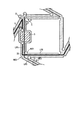
- a flexible insulating base material and a plurality of wirings provided on one surface side of the insulating base material are provided, and the insulating base material is a thinned first region. And a second region having a larger film thickness than the first region, the first region having a first lower surface, the second region having a second lower surface, the first lower surface and the first lower surface, A flexible substrate is provided, wherein the second lower surface is formed on a surface side of the insulating base material opposite to the surface side on which the wiring is provided, and the first lower surface has an inclined portion that is inclined toward the second lower surface.
- a flexible insulating base material and a plurality of wirings provided on the insulating base material are provided, and the insulating base material has an upper surface, a lower surface, and the upper surface in a sectional shape.
- a flexible substrate having a first side surface and a second side surface connecting the lower surface and one of the first side surface and the second side surface is tapered.
- a flexible insulating base material and a plurality of wirings provided on the insulating base material are provided, and the insulating base material has a first line portion and the first wiring portion in plan view.
- a first cutout portion is provided inside, a second cutout portion is provided outside the intersection portion, and a third cutout portion is provided inside the intersection portion where the second portion and the third portion intersect.
- a flexible substrate is provided.
- FIG. 1 is a schematic plan view of a flexible substrate according to the first embodiment.
- FIG. 2 is a schematic plan view in which a part of the flexible substrate is enlarged.
- FIG. 3 is a schematic sectional view of a part of the flexible substrate indicated by F3A-F3B in FIG.
- FIG. 4 is a schematic cross-sectional view of a part of the flexible substrate indicated by F4A-F4B in FIG.
- FIG. 5 is a graph showing the characteristics of deformation when the flexible substrate is expanded.
- FIG. 6 is a plan view showing a portion of the flexible substrate where cracks are likely to occur.
- FIG. 7 is a plan view showing another shape of the insulating base material.
- FIG. 8 is a plan view showing a part of the insulating base material shown in FIG. 7.
- FIG. 9 is a cross-sectional view showing the shape of the insulating base material in the second embodiment.
- FIG. 10 is a figure which shows the insulation base material of 2nd Embodiment in a meander structure.
- FIG. 11 is a plan view showing the shape of the insulating base material in the third embodiment.
- FIG. 1 is a schematic plan view of a flexible substrate 100 according to the first embodiment.
- the first direction D1, the second direction D2, the third direction D3, the fourth direction D4, and the fifth direction D5 are defined.
- the first direction D1, the second direction D2, the third direction D3, and the fourth direction D4 are all parallel to the main surface of the flexible substrate 100 and intersect with each other.
- the fifth direction D5 is a direction perpendicular to the first direction D1, the second direction D2, the third direction D3, and the fourth direction D4, and corresponds to the thickness direction of the flexible substrate 100.
- the first direction D1 and the second direction D2 intersect perpendicularly in the present embodiment, but may intersect at an angle other than vertical.
- the third direction D3 and the fourth direction D4 intersect perpendicularly in the present embodiment, but may intersect at an angle other than vertical.
- the flexible substrate 100 includes a plurality of scanning lines 1, a plurality of signal lines 2, and a plurality of electrical elements 3.
- the scanning line 1 and the signal line 2 are an example of wiring included in the flexible substrate 100.
- the scanning line 1 and the signal line 2 can be formed of, for example, a metal material or a transparent conductive material, and may have a single layer structure or a laminated structure.
- the flexible substrate 100 may include, in addition to the scanning line 1 and the signal line 2, another type of wiring such as a power supply line that supplies power to the electrical element 3.
- the plurality of scanning lines 1 extend in the first direction D1 as a whole and are arranged in the second direction D2.
- the plurality of signal lines 2 extend in the second direction D2 as a whole and are arranged in the first direction D1.
- the scanning line 1 has a wavy shape in which a straight line portion parallel to the first direction D1, a straight line portion parallel to the third direction D3, and a straight line portion parallel to the second direction D2 are sequentially repeated.
- the signal line 2 has a wavy shape in which a straight line portion parallel to the second direction D2, a straight line portion parallel to the fourth direction D4, and a straight line portion parallel to the first direction D1 are sequentially repeated.
- a polygonal area A is formed by two adjacent scanning lines 1 and two adjacent signal lines 2.
- the region A having the same shape is repeated in the first direction D1 and the second direction D2.
- the electric element 3 is electrically connected to the scanning line 1 and the signal line 2.
- the electrical element 3 is arranged in a portion where the scanning line 1 and the signal line 2 are parallel to the second direction D2.
- the arrangement position of the electrical element 3 is not limited to this example.
- the electric element 3 is a sensor, a semiconductor element, an actuator, or the like.
- the sensor an optical sensor that receives visible light or near infrared light, a temperature sensor, a pressure sensor, a touch sensor, or the like can be applied.
- a light emitting element, a light receiving element, a diode, a transistor, or the like can be used as the semiconductor element.
- the electric element 3 is a light emitting element, a flexible display having flexibility and stretchability can be realized.
- the light emitting element for example, a light emitting diode having a size of about 100 ⁇ m such as a mini LED or a micro LED, or an organic electroluminescence element can be applied.
- the electric element 3 is an actuator, for example, a piezo element can be applied.
- the electrical element 3 is not limited to the one illustrated here, and other elements having various functions can be applied.
- the electric element 3 may be a capacitor or a resistor.
- the scanning line 1 supplies a scanning signal to the electric element 3.
- the signal line 2 is supplied with the output signal from the electric element 3.
- a drive signal is supplied to the signal line 2.
- a controller including a scan signal supply source, a drive signal supply source, a processor that processes an output signal, or the like may be provided in the flexible substrate 100 or in a device connected to the flexible substrate 100.
- FIG. 2 is a schematic plan view in which a part of the flexible substrate 100 is enlarged.
- the scanning line 1 and the signal line 2 are shown in a state of being close to each other and extending in parallel, but actually, as will be described later with reference to FIG. 3, the scanning line 1 and the signal line 2 are shown.
- the flexible substrate 100 includes a flexible insulating base material 4 that supports the scanning lines 1 and the signal lines 2.
- the insulating base material 4 can be formed of, for example, polyimide, but is not limited to this example.
- the insulating base material 4 includes a plurality of line portions 41, a plurality of line portions 42 (dummy line portions), and a plurality of island-shaped portions 43.
- the line portion 41 overlaps at least one of the scanning line 1 and the signal line 2.
- the line portion 42 does not overlap with the scanning line 1 or the signal line 2.
- the line portion 41 and the line portion 42 are both linear.
- the island portion 43 overlaps with the electrical element 3 and is connected to the line portion 41.
- the line portion 41 and the line portion 42 form a polygonal first opening AP1 and a polygonal second opening AP2 different from the first opening AP1.
- the first opening AP1 is a star-shaped octagon having eight corners C1 to C8.
- the second opening AP2 is a rectangle having four corners C7 to C10.
- the corner portions C1 to C10 are portions in which two or more line portions 41 or line portions 41 and 42 are connected at different angles.
- the shapes of the first opening AP1 and the second opening AP2 are not limited to these examples, and various shapes can be adopted.
- the line 41 between the corners C2 and C3 and the line 41 between the corners C6 and C7 overlap the scanning line 1 and are parallel to the third direction D3.
- the line portion 41 between the corner portions C1 and C8 and the line portion 41 between the corner portions C4 and C5 overlap the signal line 2 and are parallel to the fourth direction D4.
- the first opening AP1 and the second opening AP2 are composed of the plurality of line portions 41 and 42 extending in the four different directions.
- the first opening AP1 and the second opening AP2 are included in one area A.
- the first opening AP1 and the second opening AP2 correspond to two areas obtained by dividing the area A by the line portion 42.
- the line portion 42 is arranged at the boundary between the first opening AP1 and the second opening AP2.
- the internal angle ⁇ 1 of the first opening AP1 at the corners C1, C3, C5, C7 is smaller than the internal angle ⁇ 2 of the first opening AP1 at the corners C2, C4, C6, C8 ( ⁇ 1 ⁇ 2).
- the interior angle ⁇ 1 is an acute angle ( ⁇ 1 ⁇ 90°) and the interior angle ⁇ 2 is an angle exceeding 180° ( ⁇ 2>180°).
- the shape of the first opening AP1 is 4-fold symmetry, which is the same shape when rotated by 90°.
- the first aperture AP1 may have rotational symmetry of four times or more, such as five-fold symmetry and six-fold symmetry. Further, the first opening AP1 may have a symmetry of three times or less.
- the island-shaped portion 43 is arranged near the center of the line portion 41 that overlaps the scanning line 1 and the signal line 2.
- the electrical element 3 is arranged above the island portion 43.
- the island-shaped portion 43 is larger than the electric element 3, and in FIG. 2, the island-shaped portion 43 protrudes from the edge of the electric element 3.
- the lengths L2 up to 43 are equal to each other. However, the length L1 and the length L2 may be different.
- the scanning line 1 has a first portion 11 shown by a solid line and a second portion 12 shown by a broken line.
- the second portion 12 overlaps the electrical element 3.
- the first portion 11 and the second portion 12 are arranged in different layers, and are electrically connected to each other through the contact holes CH1 and CH2.
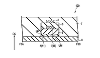
- FIG. 3 is a schematic cross-sectional view of a part of the flexible substrate 100 indicated by F3A-F3B in FIG.
- the flexible substrate 100 further includes a first organic insulating layer 5, a second organic insulating layer 6, a coating layer 7, and a support film 8 in addition to the above elements.
- the insulating base material 4 has an upper surface UP and a lower surface UN opposite to the upper surface UP.
- the scanning line 1 and the signal line 2 are provided on the upper surface UP side of the insulating base material 4.
- the first organic insulating layer 5 covers the upper surface UP of the insulating base material 4.
- the scanning line 1 (first portion 11) is arranged on the first organic insulating layer 5.
- the second organic insulating layer 6 covers the scan line 1 and the first organic insulating layer 5.
- the signal line 2 is arranged on the second organic insulating layer 6.
- the coating layer 7 covers the signal line 2, the insulating base material 4, the first organic insulating layer 5, and the second organic insulating layer 6.
- the support film 8 is in contact with the lower surface UN, and is in contact with the coating layer 7 in the region where the insulating base material 4 is not present. That is, the support film 8 overlaps with the plurality of line portions 41, 42, the first opening AP1 and the second opening AP2 in a plan view.
- first organic insulating layer 5 and the second organic insulating layer 6 may also be provided in regions (the first opening AP1 and the second opening AP2) without the insulating base material 4.
- the arrangement mode as shown in FIG. 3 is preferable.
- Both the first organic insulating layer 5 and the second organic insulating layer 6 are made of an organic material.
- the coating layer 7 is formed of parylene (polyparaxylylene), for example.
- the support film 8 may be formed by applying a resin material to the lower surfaces of the insulating base material 4 and the coating layer 7, or may be attached via an adhesive layer.
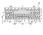
- FIG. 4 is a schematic cross-sectional view of a part of the flexible substrate 100 indicated by F4A-F4B in FIG. Below the electrical element 3, the island-shaped portion 43 of the insulating base material 4 is arranged. Thereby, the electric element 3 can be favorably supported.
- the insulating base material 4 has a partially thinned first region AR1.
- the formation position of the first region AR1 is a position where the flexible substrate 100 cannot withstand the expansion when the flexible substrate 100 is deformed by expansion and contraction, and the insulating base material 4 is apt to crack (break). Details will be described later.
- a region of the insulating base material 4 other than the first region AR1 is referred to as a second region AR2.
- the first area AR1 has a thickness T1 and the second area AR2 has a thickness T2 larger than the thickness T1. That is, the film thickness of the first region AR1 is smaller than that of the second region AR2.
- the thickness T1 is, for example, about 5 ⁇ m
- the thickness T2 is, for example, about 20 ⁇ m.
- the first region AR1 may have a thickness that can maintain the supporting function of the insulating base material 4.
- the first area AR1 has a first lower surface UN1 and the second area AR2 has a second lower surface UN2.
- the first lower surface UN1 is located closer to the wiring side such as the signal line 1 and the scanning line 2 than the second lower surface UN2. Further, the film thickness of the first region AR1 gradually increases toward the second region AR2 side. That is, the first lower surface UN1 has the inclined portion IP that is inclined toward the second lower surface UN2.
- the thinned first region AR1 is formed in a region where cracks are likely to occur.
- the first region AR1 is formed by, for example, laser ashing. As the laser, a KrF laser, an excimer laser or the like is used. A wavelength that does not react with a resin other than the insulating base material 4 is used for the laser.
- the support film 8 is in contact with the first lower surface UN1 and the second lower surface UN2.
- An inorganic insulating layer 9 (passivation layer) is formed between the electrical element 3 and the island portion 43.
- the inorganic insulating layer 9 has an island shape that overlaps with the electrical element 3 in a plan view.
- the first portion 11 of the scanning line 1 is arranged on the first organic insulating layer 5.
- the second portion 12 of the scan line 1 is arranged on the inorganic insulating layer 9 (that is, below the first organic insulating layer 5).
- the second portion 12 is electrically connected to the electric element 3. In the example of FIG. 4, the end of the second portion 12 is covered with the first organic insulating layer 5.
- the above-mentioned contact holes CH1 and CH2 are provided in the first organic insulating layer 5 in a region overlapping the island-shaped portion 43 and the inorganic insulating layer 9 in a plan view.
- the first portion 11 of the scanning line 1 is electrically connected to the second portion 12 via connecting members CM1 and CM2 arranged in the contact holes CH1 and CH2, respectively.
- the connecting members CM1 and CM2 may be a part of the first portion 11 or may be provided separately from the first portion 11.
- the insulating base material 4 has the thinned first region AR1 at a location where a crack is likely to occur.
- the flexible substrate 100 is stretched and reaches a predetermined elongation, cracks may occur in the insulating base material 4 and the wiring, but the thinning of the insulating base material 4 improves the elongation up to the cracking. can do. Therefore, the expansion rate of the flexible substrate 100 can be improved. Moreover, the generation of cracks can be suppressed.
- the insulating base material 4 has the first opening AP1 and the second opening AP2.
- the line portion 41 and the line portion 42 forming the first opening AP1 and the second opening AP2 are linear shapes that are the basis of general array design. Therefore, the pitch of the scanning lines 1 and the signal lines 2 can be made narrower and the density of the electrical elements 3 can be made much easier than when a curved pattern such as a meander shape is used.
- the line part 42 does not overlap with the scanning line 1 or the signal line 2. In this way, by providing the line portion 42 that does not support the wiring, it is possible to realize the preferable shapes of the first opening AP1 and the second opening AP2 regardless of the shapes of the scanning line 1 and the signal line 2.
- the first opening AP1 and the second opening AP2 are included in a region A defined by two adjacent scanning lines 1 and two adjacent signal lines 2. Since the regions A are arranged in a matrix on the entire flexible substrate 100, the first openings AP1 and the second openings AP2 are also dispersed and arranged on the entire flexible substrate 100. As a result, it is possible to impart good stretchability and flexibility to the wide range of the flexible substrate 100.
- the first opening AP1 has a 4-fold symmetrical shape.
- the elasticity and the direction dependency of flexibility of the flexible substrate 100 can be reduced as compared with the case where the first opening AP1 has a two-fold symmetrical shape.
- the first opening AP1 includes an interior angle ⁇ 2 of 180° or more. With such a shape including a large internal angle, the area of the first opening AP1 can be reduced as compared with the case where the first opening AP1 is formed only by the internal angle less than 180°. As a result, the scanning lines 1, the signal lines 2 and the electrical elements 3 can be formed with high density.
- an island-shaped inorganic insulating layer 9 is arranged between the electric element 3 and the insulating base material 4. Since the electrical element 3 and the second portion 12 of the scanning line 1 are protected by the inorganic insulating layer 9, the reliability of the flexible substrate 100 can be improved. On the other hand, the inorganic film is more likely to be cracked than the organic film. Therefore, when wiring is formed on the inorganic film, disconnection due to the crack may occur. However, in FIG. 4, the inorganic insulating layer 9 is not provided below the first portion 11 of the scanning line 1 or the signal line 2. Therefore, disconnection of the scanning line 1 and the signal line 2 is unlikely to occur. Further, if the inorganic insulating layer 9 is provided over the entire flexible substrate 100, the stretchability and flexibility of the flexible substrate 100 may be impaired. However, if the inorganic insulating layer 9 is formed in an island shape, Problem does not occur.
- the degree of freedom of design in the vicinity of the electric element 3 is improved. .. Since these contact holes CH1 and CH2 are provided above the inorganic insulating layer 9, the reliability at the connection position of the first portion 11 and the second portion 12 is also increased.
- the electric element 3 is arranged in the line portion 41, and is located at a position apart from the connection point between the line portions 41. As a result, even when the flexible substrate 100 is expanded or contracted or bent, stress is unlikely to be transmitted to the vicinity of the electrical element 3. Therefore, the reliability of the electric element 3 is improved. As described above, if the lengths L1 and L2 from both ends of the line portion 41 to the island-shaped portion 43 are equal, the stress applied to the electrical element 3 can be reduced extremely well. In addition to the above, various suitable effects can be obtained from this embodiment.
- FIG. 5 is a graph showing the characteristic of deformation when the flexible substrate 100 is expanded.
- the vertical axis of the graph indicates the tensile force F[N].
- the horizontal axis of the graph indicates the extension width X [mm].
- the in-plane deformation means deformation in a direction parallel to the D1-D2 plane defined by the first direction D1 and the second direction D2.
- the flexible substrate 100 switches from a certain extension or more to an out-of-plane deformation.
- the out-of-plane deformation corresponds to the case of being deformed in the direction twisted with respect to the D1-D2 plane, that is, the fifth direction D5.
- the expansion rate of the flexible substrate 100 can be increased.
- the shape of the opening of the insulating base material 4 and the shape of the region formed by the scanning line 1 and the signal line 2 are not limited to those disclosed in the above embodiment.
- the insulating base material 4 may not have the line portion 42 that does not overlap with the scanning line 1 or the signal line 2.
- the insulating base material 4 may include a curved line portion in at least a part thereof in addition to the linear line portion.
- the insulating base material 4 may have a corrugated shape as shown in FIG. 7 or may have various shapes such as a spiral shape.
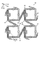
- FIG. 6 is a plan view showing a portion of the flexible substrate 100 where cracks are likely to occur.
- a portion surrounded by a circle in the drawing is likely to be cracked, and thus corresponds to the first region AR1 in which the insulating base material 4 is thinned.
- the first region AR1 is, for example, in the center of the line portion 41 extending in the first direction D1, in the center of the line portion 41 extending in the second direction D2, or in the center of the line portion 42 extending in the second direction D2. positioned. Further, the first region AR1 is located in the vicinity of the corners C2, C3, C6, C7 of the line portion 42 extending in the third direction D3, and of the line portion 42 extending in the fourth direction D4.
- the flexible substrate 100 has the same layer structure as that of the first region AR1 of the insulating base material 4 shown in FIG. As a result, the out-of-plane deformation can be promoted only at the places where cracks are likely to occur, and a margin for fracture elongation can be secured.
- FIG. 7 is a plan view showing another shape of the insulating base material 4.
- the insulating base material 4 includes a plurality of first portions PT1 extending in the first direction D1 and arranged side by side in the second direction D2 and a plurality of first portions PT1 extending in the second direction D2 and arranged side by side in the first direction D1. And a second portion PT2.
- the first portion PT1 and the second portion PT2 are each wave-shaped.
- the insulating base material 4 has an intersection portion IT between the first portion PT1 and the second portion PT2.
- the scanning line 1 is located on the first portion PT1, extends in the first direction D1, and is arranged in the second direction D2.
- the signal line 2 is located on the second portion PT2, extends in the second direction D2, and is arranged in the first direction D1.
- the electrical element 3 is located on the intersection IT.
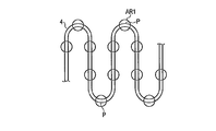
- FIG. 8 is a plan view showing a part of the insulating base material 4 shown in FIG.
- the portion surrounded by a circle in the drawing corresponds to the first area AR1 where cracks are likely to occur.
- the first area AR1 is located near the top P of the waveform. Further, the first region AR1 is located between the tops P at a position where the bending is maximized when the flexible substrate 100 extends.
- the insulating base material 4 is thinned as in the first region AR1 shown in FIG. Even with such a pattern of the insulating base material 4, the same effect as that of the pattern shown in FIG. 6 can be obtained.
- FIG. 9 is a sectional view showing the shape of the insulating base material 4 in the second embodiment.
- the support film 8 and the coating layer 7 are omitted from the cross section shown in FIG.
- the insulating base material 4 has an upper surface UP, a lower surface UN, and a first side surface SD1 and a second side surface SD2 connecting the upper surface UP and the lower surface UN in a sectional shape.
- the upper surface UP is in contact with the first organic insulating layer 5.
- the width W1 of the upper surface UP is smaller than the width W2 of the lower surface UN.
- the first side surface SD1 is tapered and the second side surface SD2 is not tapered.
- the second side surface SD2 is tapered and the first side surface SD1 is not tapered.
- the width W1 of the upper surface UP is 10 ⁇ m or more, and the width W2 of the lower surface UN is 50 ⁇ m or less.
- the width W2 of the lower surface UN is smaller than the width W1 of the upper surface UP.
- the first side surface SD1 is tapered and the second side surface SD2 is not tapered.
- the second side surface SD2 is tapered and the first side surface SD1 is not tapered.
- the width W2 of the lower surface UN is 10 ⁇ m or more, and the width W1 of the upper surface UP is 50 ⁇ m or less.
- the tapered shape as shown in FIGS. 9A to 9D is formed by, for example, laser ashing.
- the insulating base material 4 may be formed by irradiating the insulating base material 4 with a laser in a direction oblique to the normal line of the main surface of the substrate.
- the laser a KrF laser, an excimer laser or the like is used.
- a wavelength that does not react with a resin other than the insulating base material 4 is used for the laser.
- one of the first side surface SD1 and the second side surface SD2 is formed in a tapered shape, so that the insulating base material 4 is easily twisted. That is, the insulating base material 4 is configured to promote the out-of-plane deformation, and the elongation of the flexible substrate 100 until the flexible substrate 100 expands and breaks can be improved. Therefore, the expansion rate of the flexible substrate 100 can be improved. Moreover, the generation of cracks can be suppressed.
- FIG. 10 is a figure which shows the insulating base material 4 of 2nd Embodiment in a meander structure.
- FIG. 10A is a plan view of a part of the meander structure.
- 10(2) and 10(3) are cross-sectional views of the insulating base material 4 in the regions a to f shown in FIG. 10(1).
- the regions a, c, and e are easily twisted counterclockwise, and the regions b, d, and f are easily twisted clockwise.
- the direction of twist is determined by the taper of the insulating base material 4.
- the width of the upper surface UP is smaller than the width of the lower surface UN.
- the second side surface SD2 is tapered, and it is easy to twist counterclockwise.
- the first side surface SD1 has a tapered shape, and tends to be twisted clockwise.
- the width of the upper surface UP is larger than the width of the lower surface UN.
- the first side surface SD1 is tapered, and it is easy to twist counterclockwise.
- the second side surface SD2 is tapered, and it is easy to twist clockwise.
- the force in the direction of repulsing the twist can be suppressed, and the twist of the insulating base material 4 can be promoted.
- the combination of the tapers be such that the clockwise and counterclockwise forces are equal.
- the insulating base material 4 may be formed in a tapered shape only in a portion where a crack is likely to occur, or may be tapered in its entirety.
- FIG. 11 is a plan view showing the shape of the insulating base material 4 in the third embodiment.
- the insulating base material 4 has a first line portion LP1, a second line portion LP2, and a third line portion LP3 in a plan view.
- the first line portion LP1, the second line portion LP2, and the third line portion LP3 intersect each other at an intersection IS.
- the first line portion LP1 and the second line portion LP2 intersect at a substantially right angle.
- the second portion LP2 and the third portion LP3 intersect at an acute internal angle ⁇ 1.
- the insulating base material 4 has a first cutout portion NT1 on the inner side where the first line portion LP1 and the second line portion LP2 intersect at the intersecting portion IS, and a second cutout portion NT2 on the outer side. There is. Similarly, in the intersecting portion IS, a third cutout portion is provided inside the intersecting portion of the second portion LP2 and the third portion LP3.
- the notch is formed, for example, by adjusting the resist mask and laser ashing conditions.
- the laser a KrF laser, an excimer laser or the like is used.
- stress is applied to the inside as shown by arrow g on the outside where the first line LP1 and the second line LP2 intersect.
- stress is applied to the outer side as shown by the arrow h.
- stress is applied to the outer side as shown by the arrow i.
- these stresses can be released by forming the first cutout portion NT1, the second cutout portion NT2, and the third cutout portion NT3. Therefore, it is possible to improve the elongation until the flexible substrate 100 expands and breaks. Therefore, the expansion rate of the flexible substrate 100 can be improved. Moreover, the generation of cracks can be suppressed.
Landscapes
- Engineering & Computer Science (AREA)
- Microelectronics & Electronic Packaging (AREA)
- Structure Of Printed Boards (AREA)
Abstract
本実施形態に係るフレキシブル基板は、可撓性の絶縁基材と、前記絶縁基材の一方の面側に設けられた複数の配線と、を備え、前記絶縁基材は、薄膜化された第1領域と、前記第1領域より膜厚が大きい第2領域と、を有し、前記第1領域は第1下面を有し、前記第2領域は第2下面を有し、前記第1下面と前記第2下面は、前記絶縁基材の配線が設けられた面側と反対側の面側に形成され、前記第1下面は、前記第2下面にかけて傾斜した傾斜部を有する。
Description
本発明の実施形態は、フレキシブル基板に関する。
近年、可撓性及び伸縮性を有したフレキシブル基板の利用が種々の分野で検討されている。一例を挙げると、マトリクス状に電気的素子が配列されたフレキシブル基板を電子機器の筐体や人体等の曲面に貼り付ける利用形態が考えられる。電気的素子としては、例えばタッチセンサや温度センサ等の各種センサや表示素子が適用され得る。
フレキシブル基板においては、屈曲や伸縮による応力で配線が損傷しないように対策を講じる必要がある。このような対策としては、例えば、配線を支持する基材にハニカム形状の開口を設けることや、配線を蛇行した形状(ミアンダ形状)とすることが提案されている。
本実施形態の目的は、伸長率を向上することが可能、及び、クラックの発生を抑制することが可能なフレキシブル基板を提供することにある。
本実施形態によれば、可撓性の絶縁基材と、前記絶縁基材の一方の面側に設けられた複数の配線と、を備え、前記絶縁基材は、薄膜化された第1領域と、前記第1領域より膜厚が大きい第2領域と、を有し、前記第1領域は第1下面を有し、前記第2領域は第2下面を有し、前記第1下面と前記第2下面は、前記絶縁基材の配線が設けられた面側と反対側の面側に形成され、前記第1下面は、前記第2下面にかけて傾斜した傾斜部を有する、フレキシブル基板が提供される。
本実施形態によれば、可撓性の絶縁基材と、前記絶縁基材に設けられた複数の配線と、を備え、前記絶縁基材は、断面形状において上面と、下面と、前記上面と前記下面とをつなぐ第1側面及び第2側面と、を有し、前記第1側面及び前記第2側面の一方がテーパー状である、フレキシブル基板が提供される。
本実施形態によれば、可撓性の絶縁基材と、前記絶縁基材に設けられた複数の配線と、を備え、前記絶縁基材は、平面視で、第1線部と、前記第1線部と交差する第2線部と、前記第1線部及び前記第2線部と交差する第3線部と、前記第1線部と前記第2線部とが交差する交差部の内側に第1切り欠き部と、前記交差部の外側に第2切り欠き部と、前記第2部分と前記第3部分とが交差する前記交差部の内側に第3切り欠き部と、を有する、フレキシブル基板が提供される。
以下、本実施形態について、図面を参照しながら説明する。なお、開示はあくまで一例に過ぎず、当業者において、発明の主旨を保っての適宜変更について容易に想到し得るものについては、当然に本発明の範囲に含有されるものである。また、図面は、説明をより明確にするため、実際の態様に比べて、各部の幅、厚さ、形状等について模式的に表される場合があるが、あくまで一例であって、本発明の解釈を限定するものではない。また、本明細書と各図において、既出の図に関して前述したものと同一又は類似した機能を発揮する構成要素には同一の参照符号を付し、重複する詳細な説明を適宜省略することがある。
[第1実施形態]
図1は、第1実施形態に係るフレキシブル基板100の概略的な平面図である。
本実施形態においては、図示したように第1方向D1、第2方向D2、第3方向D3、第4方向D4、及び、第5方向D5を定義する。第1方向D1、第2方向D2、第3方向D3、及び、第4方向D4は、何れもフレキシブル基板100の主面と平行であり、互いに交わる方向である。また、第5方向D5は、第1方向D1、第2方向D2、第3方向D3、第4方向D4に対して垂直な方向であり、フレキシブル基板100の厚さ方向に相当する。第1方向D1と第2方向D2は、本実施形態では垂直に交わるが、垂直以外の角度で交わってもよい。また、第3方向D3と第4方向D4は、本実施形態では垂直に交わるが、垂直以外の角度で交わってもよい。
図1は、第1実施形態に係るフレキシブル基板100の概略的な平面図である。
本実施形態においては、図示したように第1方向D1、第2方向D2、第3方向D3、第4方向D4、及び、第5方向D5を定義する。第1方向D1、第2方向D2、第3方向D3、及び、第4方向D4は、何れもフレキシブル基板100の主面と平行であり、互いに交わる方向である。また、第5方向D5は、第1方向D1、第2方向D2、第3方向D3、第4方向D4に対して垂直な方向であり、フレキシブル基板100の厚さ方向に相当する。第1方向D1と第2方向D2は、本実施形態では垂直に交わるが、垂直以外の角度で交わってもよい。また、第3方向D3と第4方向D4は、本実施形態では垂直に交わるが、垂直以外の角度で交わってもよい。
フレキシブル基板100は、複数の走査線1と、複数の信号線2と、複数の電気的素子3と、を備えている。走査線1及び信号線2は、フレキシブル基板100が備える配線の一例である。走査線1及び信号線2は、例えば金属材料や透明導電材料で形成することができ、単層構造であってもよいし積層構造であってもよい。フレキシブル基板100は、走査線1及び信号線2の他に、電気的素子3に給電する電源線などの他種の配線を備えてもよい。
複数の走査線1は、全体的に第1方向D1に延びるとともに、第2方向D2に並んでいる。複数の信号線2は、全体的に第2方向D2に延びるとともに、第1方向D1に並んでいる。具体的には、走査線1は、第1方向D1と平行な直線部分、第3方向D3と平行な直線部分、第2方向D2と平行な直線部分が順に繰り返す波型の形状を有している。同様に、信号線2は、第2方向D2と平行な直線部分、第4方向D4と平行な直線部分、第1方向D1と平行な直線部分が順に繰り返す波型の形状を有している。
隣り合う2本の走査線1と隣り合う2本の信号線2とにより、多角形状の領域Aが形成されている。図1の例においては、同じ形状の領域Aが第1方向D1及び第2方向D2に繰り返されている。
電気的素子3は、走査線1及び信号線2と電気的に接続されている。図示した例においては、走査線1及び信号線2が第2方向D2と平行な部分に電気的素子3が配置されている。ただし、電気的素子3の配置位置はこの例に限られない。
例えば電気的素子3は、センサ、半導体素子、又はアクチュエータなどである。例えばセンサとしては、可視光や近赤外光を受光する光学センサ、温度センサ、圧力センサ、又はタッチセンサなどを適用できる。例えば半導体素子としては、発光素子、受光素子、ダイオード、又はトランジスタなどを適用できる。電気的素子3が発光素子である場合、可撓性及び伸縮性を有したフレキシブルディスプレイを実現できる。発光素子としては、例えばミニLEDやマイクロLEDといった100μm前後の大きさを有する発光ダイオードや有機エレクトロルミネッセンス素子を適用できる。電気的素子3がアクチュエータである場合、例えばピエゾ素子を適用できる。なお、電気的素子3は、ここで例示したものに限られず、その他にも種々の機能を有した素子を適用し得る。電気的素子3は、コンデンサや抵抗などであってもよい。
走査線1は、電気的素子3に走査信号を供給する。例えば電気的素子3がセンサのような信号の出力を伴うものである場合、信号線2には電気的素子3からの出力信号が供給される。また、例えば電気的素子3が発光素子やアクチュエータのように入力される信号に応じて作動するものである場合、信号線2には駆動信号が供給される。走査信号の供給源、駆動信号の供給源又は出力信号を処理するプロセッサなどを含むコントローラは、フレキシブル基板100に設けられてもよいし、フレキシブル基板100に接続される機器に設けられてもよい。
図2は、フレキシブル基板100の一部を拡大した概略的な平面図である。
電気的素子3の近傍において、走査線1及び信号線2が近接して平行に延在する状態を示しているが、実際には図3を用いて後述するように走査線1と信号線2がフレキシブル基板100の厚さ方向に積層されている。
電気的素子3の近傍において、走査線1及び信号線2が近接して平行に延在する状態を示しているが、実際には図3を用いて後述するように走査線1と信号線2がフレキシブル基板100の厚さ方向に積層されている。
フレキシブル基板100は、走査線1及び信号線2を支持する可撓性の絶縁基材4を備えている。絶縁基材4は、例えばポリイミドで形成することができるが、この例に限られない。
絶縁基材4は、複数の線部41と、複数の線部42(ダミー線部)と、複数の島状部43と、を含む。線部41は、走査線1及び信号線2の少なくとも一方と重畳している。線部42は、走査線1及び信号線2の何れとも重畳していない。線部41及び線部42は、何れも直線状である。島状部43は、電気的素子3と重畳し、線部41と接続されている。
線部41及び線部42により、多角形状の第1開口AP1と、第1開口AP1とは異なる多角形状の第2開口AP2とが形成される。図2の例において、第1開口AP1は8つの角部C1乃至C8を有する星型の8角形である。第2開口AP2は、4つの角部C7乃至C10を有する矩形である。角部C1乃至C10は、2つ以上の線部41、又は、線部41と線部42が互いに異なる角度で接続される部分である。第1開口AP1及び第2開口AP2の形状はこれらの例に限られず、種々の形状を採用し得る。
角部C1と角部C2の間の線部41、及び、角部C7と角部C10の間の線部41は、走査線1と重畳しており、第1方向D1と平行である。角部C5と角部C6の間の線部41、及び、角部C8と角部C9の間の線部41は、信号線2と重畳しており、第1方向D1と平行である。
角部C3と角部C4の間の線部41、及び、角部C9と角部C10の間の線部41は、走査線1及び信号線2と重畳しており、第2方向D2と平行である。角部C7と角部C8の間の線部42は、走査線1及び信号線2の何れとも重畳しておらず、第2方向D2と平行である。
角部C2と角部C3の間の線部41、及び、角部C6と角部C7の間の線部41は、走査線1と重畳しており、第3方向D3と平行である。角部C1と角部C8の間の線部41、及び、角部C4と角部C5の間の線部41は、信号線2と重畳しており、第4方向D4と平行である。
このように、第1開口AP1及び第2開口AP2は、4方向の異なる方向にそれぞれ延びる複数の線部41、42によって構成されている。第1開口AP1及び第2開口AP2は、1つの領域Aに含まれる。第1開口AP1及び第2開口AP2は、領域Aを線部42で分けた2つの領域に相当する。他の観点からいえば、線部42は、第1開口AP1及び第2開口AP2の境界に配置されている。2つ以上の線部42を領域Aに設けることで、3つ以上の開口を領域A内に形成してもよい。
角部C1、C3、C5、C7における第1開口AP1の内角θ1は、角部C2、C4、C6、C8における第1開口AP1の内角θ2よりも小さい(θ1<θ2)。図2の例において、内角θ1は鋭角であり(θ1<90°)、内角θ2は180°を超える角度である(θ2>180°)。
第1開口AP1の形状は、90°回転させると同じ形状となる4回対称である。この例に限られず、第1開口AP1は、5回対称や6回対称などの4回以上の回転対称性を有してもよい。また、第1開口AP1は、3回以下の対称性を有してもよい。
島状部43は、走査線1及び信号線2と重畳する線部41の中央付近に配置されている。電気的素子3は、島状部43の上方に配置されている。島状部43は電気的素子3よりも大きく、図2においては電気的素子3の縁から島状部43がはみ出ている。例えば角部C3、C4の間の線部41に着目すると、この線部41の図中上側の端部から島状部43までの長さL1と、図中下側の端部から島状部43までの長さL2とは、互いに等しい。ただし、長さL1と長さL2が異なってもよい。
走査線1は、実線で示す第1部分11と、破線で示す第2部分12とを有している。第2部分12は、電気的素子3と重畳している。第1部分11と第2部分12は、互いに異なる層に配置されており、コンタクトホールCH1、CH2を通じて電気的に接続されている。
図3は、図2においてF3A-F3Bで示すフレキシブル基板100の一部の概略的な断面図である。
フレキシブル基板100は、上述の要素の他に、第1有機絶縁層5と、第2有機絶縁層6と、コーティング層7と、支持フィルム8と、をさらに備えている。
フレキシブル基板100は、上述の要素の他に、第1有機絶縁層5と、第2有機絶縁層6と、コーティング層7と、支持フィルム8と、をさらに備えている。
絶縁基材4は、上面UPと、上面UPの反対側の下面UNと、を有している。走査線1及び信号線2は、絶縁基材4の上面UP側に設けられている。第1有機絶縁層5は、絶縁基材4の上面UPを覆っている。走査線1(第1部分11)は、第1有機絶縁層5の上に配置されている。第2有機絶縁層6は、走査線1及び第1有機絶縁層5を覆っている。信号線2は、第2有機絶縁層6の上に配置されている。コーティング層7は、信号線2、絶縁基材4、第1有機絶縁層5及び第2有機絶縁層6を覆っている。支持フィルム8は、下面UNに接し、絶縁基材4が無い領域においては、コーティング層7に接している。すなわち、支持フィルム8は、平面視において複数の線部41、42、第1開口AP1及び第2開口AP2と重畳している。
なお、第1有機絶縁層5及び第2有機絶縁層6は、絶縁基材4が無い領域(第1開口AP1及び第2開口AP2)にも設けられてもよい。ただし、フレキシブル基板100の可撓性及び伸縮性の観点からは、図3に示すような配置態様が好ましい。
第1有機絶縁層5及び第2有機絶縁層6は、何れも有機材料で形成されている。コーティング層7は、例えばパリレン(ポリパラキシリレン)で形成されている。支持フィルム8は、絶縁基材4およびコーティング層7の下面に樹脂材料を塗布して形成されてもよいし、接着層を介して貼り付けられてもよい。
図4は、図2においてF4A-F4Bで示すフレキシブル基板100の一部の概略的な断面図である。
電気的素子3の下方には、絶縁基材4の島状部43が配置されている。これにより、電気的素子3を良好に支持できる。絶縁基材4は、部分的に薄膜化された第1領域AR1を有している。第1領域AR1の形成位置は、フレキシブル基板100が伸縮によって変形した際、伸長に耐えられず絶縁基材4にクラック(破断)が生じやすい位置となる。詳しくは後述する。また、絶縁基材4のうち、第1領域AR1以外の領域を第2領域AR2とする。第1領域AR1は厚さT1を有し、第2領域AR2は厚さT1より大きい厚さT2を有している。すなわち、第1領域AR1の膜厚は、第2領域AR2の膜厚より小さく形成されている。厚さT1は、例えば、約5μmであり、厚さT2は、例えば、約20μmである。なお、第1領域AR1は、絶縁基材4の支持機能を保つことができる厚さであればよい。
電気的素子3の下方には、絶縁基材4の島状部43が配置されている。これにより、電気的素子3を良好に支持できる。絶縁基材4は、部分的に薄膜化された第1領域AR1を有している。第1領域AR1の形成位置は、フレキシブル基板100が伸縮によって変形した際、伸長に耐えられず絶縁基材4にクラック(破断)が生じやすい位置となる。詳しくは後述する。また、絶縁基材4のうち、第1領域AR1以外の領域を第2領域AR2とする。第1領域AR1は厚さT1を有し、第2領域AR2は厚さT1より大きい厚さT2を有している。すなわち、第1領域AR1の膜厚は、第2領域AR2の膜厚より小さく形成されている。厚さT1は、例えば、約5μmであり、厚さT2は、例えば、約20μmである。なお、第1領域AR1は、絶縁基材4の支持機能を保つことができる厚さであればよい。
また、第1領域AR1は、第1下面UN1を有し、第2領域AR2は、第2下面UN2を有している。第1下面UN1は、第2下面UN2よりも信号線1や走査線2などの配線側に位置している。また、第1領域AR1は、第2領域AR2側に向かって膜厚が段々と厚くなっている。すなわち、第1下面UN1は、第2下面UN2にかけて傾斜した傾斜部IPを有している。このように薄膜化された第1領域AR1は、クラックが発生しやすい領域に形成されている。第1領域AR1は、例えば、レーザーアッシングによって形成されている。レーザーとしては、KrFレーザー、エキシマレーザーなどが用いられる。また、レーザーには、絶縁基材4以外の樹脂と反応しない波長が用いられる。
支持フィルム8は、第1下面UN1及び第2下面UN2に接している。電気的素子3と島状部43の間には、無機絶縁層9(パッシベーション層)が形成されている。無機絶縁層9は、平面視においては電気的素子3と重畳する島状である。走査線1の第1部分11は、第1有機絶縁層5の上に配置されている。走査線1の第2部分12は、無機絶縁層9の上(すなわち第1有機絶縁層5の下)に配置されている。第2部分12は、電気的素子3と電気的に接続されている。図4の例においては、第2部分12の端部が第1有機絶縁層5に覆われている。
上述のコンタクトホールCH1、CH2は、島状部43及び無機絶縁層9と平面視で重畳する領域において、第1有機絶縁層5に設けられている。走査線1の第1部分11は、コンタクトホールCH1、CH2にそれぞれ配置された接続部材CM1、CM2を介して第2部分12と電気的に接続されている。接続部材CM1、CM2は、第1部分11の一部であってもよいし、第1部分11とは別途に設けられてもよい。
本実施形態によれば、絶縁基材4は、クラックが生じやすい箇所において、薄膜化された第1領域AR1を有している。フレキシブル基板100が伸長され所定の伸度に達すると絶縁基材4や配線にクラックが発生する恐れがあるが、絶縁基材4が薄膜化されることで、クラックに至るまでの伸度を向上することができる。よって、フレキシブル基板100の伸長率を向上することができる。また、クラックの発生を抑制することができる。
また、本実施形態によれば、絶縁基材4が第1開口AP1と第2開口AP2を有している。このように、異なる形状の第1開口AP1及び第2開口AP2を設けることで、様々な方向への伸縮性及び可撓性をフレキシブル基板100に与えることができる。また、第1開口AP1及び第2開口AP2を構成する線部41及び線部42は、一般的なアレイ設計の基本となる直線状である。したがって、ミアンダ形状などの曲線状のパターンを用いる場合に比べて、走査線1及び信号線2の狭ピッチ化や電気的素子3の高密度化が極めて容易となる。
線部42は、走査線1及び信号線2の何れとも重畳しない。このように、配線を支持しない線部42を設けることで、走査線1及び信号線2の形状によらずに好適な第1開口AP1及び第2開口AP2の形状を実現できる。
第1開口AP1及び第2開口AP2は、隣り合う2本の走査線1と隣り合う2本の信号線2とで区画される領域Aに含まれる。この領域Aは、フレキシブル基板100の全体にマトリクス状に並ぶため、第1開口AP1及び第2開口AP2もフレキシブル基板100の全体に分散して配置される。これにより、フレキシブル基板100の広範囲に良好な伸縮性及び可撓性を付与することができる。
また、図2に示した例においては、第1開口AP1が4回対称の形状である。これにより、例えば第1開口AP1が2回対称な形状である場合に比べ、フレキシブル基板100の伸縮性及び可撓性の方向依存度を低減できる。
さらに、図2に示した例においては、第1開口AP1が180°以上の内角θ2を含む。このような大きな内角を含む形状であれば、180°未満の内角のみで第1開口AP1を形成する場合に比べ、第1開口AP1の面積を低減できる。これにより、走査線1、信号線2及び電気的素子3を高密度で形成することが可能となる。
図4に示したように、電気的素子3と絶縁基材4の間には島状の無機絶縁層9が配置されている。この無機絶縁層9により電気的素子3や走査線1の第2部分12が保護されるので、フレキシブル基板100の信頼性を高めることができる。一方、無機膜は有機膜に比べてクラックが生じやすいため、無機膜の上に配線を形成した場合にはクラックに伴う断線が生じ得る。しかしながら、図4においては走査線1の第1部分11や信号線2の下方には無機絶縁層9が設けられていない。したがって、走査線1及び信号線2の断線が生じにくい。さらに、無機絶縁層9が仮にフレキシブル基板100の全体に設けられている場合にはフレキシブル基板100の伸縮性及び可撓性を阻害し得るが、島状に無機絶縁層9を形成すればこのような問題が生じない。
また、異なる層に配置された走査線1の第1部分11と第2部分12をコンタクトホールCH1、CH2で接続する構成としたことにより、電気的素子3の近傍における設計の自由度が向上する。これらのコンタクトホールCH1、CH2は、無機絶縁層9の上方に設けられているため、第1部分11と第2部分12の接続位置での信頼性も高まる。
電気的素子3は、図2に示したように、線部41に配置されており、しかも線部41同士の接続点から離れた位置にある。これにより、フレキシブル基板100が伸縮した場合や曲げられた場合でも、電気的素子3の近傍に応力が伝わりにくい。したがって、電気的素子3の信頼性が向上する。上述したように、線部41の両端部から島状部43までの長さL1、L2が等しければ、電気的素子3に加わる応力を極めて良好に低減できる。
以上の他にも、本実施形態からは種々の好適な効果を得ることができる。
以上の他にも、本実施形態からは種々の好適な効果を得ることができる。
図5は、フレキシブル基板100が伸長した際の変形の特性を示すグラフである。
グラフの縦軸は、引っ張り力F[N]を示している。グラフの横軸は、伸び幅X[mm]を示している。フレキシブル基板100を伸長させると、初期段階では、平面内変形する。ここで、平面内変形とは、第1方向D1及び第2方向D2で規定されるD1-D2平面と平行な方向に変形することである。フレキシブル基板100は、ある一定以上の伸び幅から平面外変形に切り替わる。ここで、平面外変形とは、D1-D2平面に対してねじれる方向、すなわち、第5方向D5にも変形する場合に相当する。上記した実施形態では、絶縁基材4を薄膜化することで、引っ張り力に対して平面外変形できる伸び幅を増やすことができる。そのため、フレキシブル基板100の伸長率を増やすことができる。
グラフの縦軸は、引っ張り力F[N]を示している。グラフの横軸は、伸び幅X[mm]を示している。フレキシブル基板100を伸長させると、初期段階では、平面内変形する。ここで、平面内変形とは、第1方向D1及び第2方向D2で規定されるD1-D2平面と平行な方向に変形することである。フレキシブル基板100は、ある一定以上の伸び幅から平面外変形に切り替わる。ここで、平面外変形とは、D1-D2平面に対してねじれる方向、すなわち、第5方向D5にも変形する場合に相当する。上記した実施形態では、絶縁基材4を薄膜化することで、引っ張り力に対して平面外変形できる伸び幅を増やすことができる。そのため、フレキシブル基板100の伸長率を増やすことができる。
なお、絶縁基材4が有する開口の形状や、走査線1及び信号線2で形成される領域の形状は、上記実施形態に開示したものに限られない。例えば、絶縁基材4は、走査線1及び信号線2の何れとも重畳しない線部42を有さなくてもよい。また、絶縁基材4は、直線状の線部に加え、曲線状の線部を少なくとも一部に含んでもよい。例えば、絶縁基材4は、図7に示すような波形状であっても良いし、渦巻き状など種々の形態をとることができる。
図6は、フレキシブル基板100のクラックが発生しやすい箇所を示す平面図である。
図中の丸で囲まれた部分は、クラックが発生しやすいため、絶縁基材4が薄膜化された第1領域AR1に相当する。第1領域AR1は、例えば、第1方向D1に延出する線部41の真ん中、第2方向D2に延出する線部41の真ん中、第2方向D2に延出する線部42の真ん中に位置している。また、第1領域AR1は、第3方向D3に延出する線部42のうち、角部C2、C3、C6、C7付近に位置し、第4方向D4に延出する線部42のうち、角部C1、C8、C4、C5付近に位置している。これらの第1領域AR1においては、フレキシブル基板100は、図4に示した絶縁基材4の第1領域AR1と同等の層構造を有している。これにより、クラックが発生しやすい個所のみ平面外変形を助長させ、破断伸度のマージンを確保することができる。
図中の丸で囲まれた部分は、クラックが発生しやすいため、絶縁基材4が薄膜化された第1領域AR1に相当する。第1領域AR1は、例えば、第1方向D1に延出する線部41の真ん中、第2方向D2に延出する線部41の真ん中、第2方向D2に延出する線部42の真ん中に位置している。また、第1領域AR1は、第3方向D3に延出する線部42のうち、角部C2、C3、C6、C7付近に位置し、第4方向D4に延出する線部42のうち、角部C1、C8、C4、C5付近に位置している。これらの第1領域AR1においては、フレキシブル基板100は、図4に示した絶縁基材4の第1領域AR1と同等の層構造を有している。これにより、クラックが発生しやすい個所のみ平面外変形を助長させ、破断伸度のマージンを確保することができる。
図7は、絶縁基材4の他の形状を示す平面図である。
絶縁基材4は、第1方向D1に延出し第2方向D2に並んで配置された複数の第1部分PT1と、第2方向D2に延出し第1方向D1に並んで配置された複数の第2部分PT2と、を有している。第1部分PT1及び第2部分PT2は、それぞれ波型である。また、絶縁基材4は、第1部分PT1と第2部分PT2との交差部ITを有している。走査線1は、第1部分PT1上に位置し、第1方向D1に延出し第2方向D2に並んでいる。信号線2は、第2部分PT2上に位置し、第2方向D2に延出し第1方向D1に並んでいる。電気的素子3は、交差部IT上に位置している。
絶縁基材4は、第1方向D1に延出し第2方向D2に並んで配置された複数の第1部分PT1と、第2方向D2に延出し第1方向D1に並んで配置された複数の第2部分PT2と、を有している。第1部分PT1及び第2部分PT2は、それぞれ波型である。また、絶縁基材4は、第1部分PT1と第2部分PT2との交差部ITを有している。走査線1は、第1部分PT1上に位置し、第1方向D1に延出し第2方向D2に並んでいる。信号線2は、第2部分PT2上に位置し、第2方向D2に延出し第1方向D1に並んでいる。電気的素子3は、交差部IT上に位置している。
図8は、図7に示した絶縁基材4の一部を示す平面図である。
図中の丸で囲まれた部分は、クラックが発生しやすい第1領域AR1に相当する。第1領域AR1は、波形の頂部P付近に位置している。また、第1領域AR1は、頂部P間において、フレキシブル基板100が伸長した際に曲がりが最大となる個所に位置している。これらの第1領域AR1においては、フレキシブル基板100は、図4に示した第1領域AR1と同様に絶縁基材4が薄膜化されている。このような絶縁基材4のパターンにおいても、図6に示したパターンと同様の効果を得ることができる。
図中の丸で囲まれた部分は、クラックが発生しやすい第1領域AR1に相当する。第1領域AR1は、波形の頂部P付近に位置している。また、第1領域AR1は、頂部P間において、フレキシブル基板100が伸長した際に曲がりが最大となる個所に位置している。これらの第1領域AR1においては、フレキシブル基板100は、図4に示した第1領域AR1と同様に絶縁基材4が薄膜化されている。このような絶縁基材4のパターンにおいても、図6に示したパターンと同様の効果を得ることができる。
[第2実施形態]
図9は、第2実施形態における絶縁基材4の形状を示す断面図である。
図9は、図3に示した断面から支持フィルム8及びコーティング層7を省略して示している。絶縁基材4は、断面形状において、上面UPと、下面UNと、上面UPと下面UNとをつなぐ第1側面SD1及び第2側面SD2と、を有している。上面UPは、第1有機絶縁層5に接している。
図9は、第2実施形態における絶縁基材4の形状を示す断面図である。
図9は、図3に示した断面から支持フィルム8及びコーティング層7を省略して示している。絶縁基材4は、断面形状において、上面UPと、下面UNと、上面UPと下面UNとをつなぐ第1側面SD1及び第2側面SD2と、を有している。上面UPは、第1有機絶縁層5に接している。
図9(A)及び(B)に示す例では、上面UPの幅W1は、下面UNの幅W2より小さい。図9(A)では、第1側面SD1がテーパー状であり、第2側面SD2がテーパー状ではない。図9(B)では、第2側面SD2がテーパー状であり、第1側面SD1がテーパー状ではない。図9(A)及び(B)に示す例では、上面UPの幅W1は、10μm以上であり、下面UNの幅W2は、50μm以下である。
図9(C)及び(D)に示す例では、下面UNの幅W2は、上面UPの幅W1より小さい。図9(C)では、第1側面SD1がテーパー状であり、第2側面SD2がテーパー状ではない。図9(D)では、第2側面SD2がテーパー状であり、第1側面SD1がテーパー状ではない。図9(C)及び(D)に示す例では、下面UNの幅W2は、10μm以上であり、上面UPの幅W1は、50μm以下である。図9(C)及び(D)においては、配線側の上面UPが幅広であるため、配線の位置ずれに対応することができる。
図9(A)乃至(D)に示すようなテーパー形状は、例えば、レーザーアッシングによって形成されている。また、基板主面の法線に対して斜めの方向から絶縁基材4にレーザーを照射することによって形成されても良い。レーザーとしては、KrFレーザー、エキシマレーザーなどが用いられる。また、レーザーには、絶縁基材4以外の樹脂と反応しない波長が用いられる。
第2実施形態によれば、第1側面SD1及び第2側面SD2の一方がテーパー状に形成されることによって、絶縁基材4がねじれやすくなる。すなわち、絶縁基材4の平面外変形を助長させる構成となり、フレキシブル基板100が伸長して破断に至るまでの伸度を向上することができる。よって、フレキシブル基板100の伸長率を向上することができる。また、クラックの発生を抑制することができる。
図10は、ミアンダ構造における第2実施形態の絶縁基材4を示す図である。
図10(1)は、ミアンダ構造の一部の平面図である。図10(2)及び(3)は、図10(1)に示す領域a乃至fにおける絶縁基材4の断面図である。
図10(1)は、ミアンダ構造の一部の平面図である。図10(2)及び(3)は、図10(1)に示す領域a乃至fにおける絶縁基材4の断面図である。
フレキシブル基板が伸長された際に、領域a、c、eは、半時計周りにねじれやすく、領域b、d、fは、時計周りにねじれやすい。さらに、絶縁基材4のテーパーによって、ねじれの方向が決められる。例えば、図10(2)に示す例では、(a)乃至(f)は、上面UPの幅が下面UNの幅より小さい。また、(a)(c)(e)は、第2側面SD2がテーパー状であり、半時計周りにねじれやすくなる。(b)(d)(f)は、第1側面SD1がテーパー状であり、時計周りにねじれやすくなる。すなわち、領域a、c、eは、もともと半時計周りに力がかかり、領域b、d、fは、もともと時計回りに力がかかるため、テーパー形状を形成することで、もともとの力がかかる方向にさらに力がかかりやすくなる。よって、ねじれに反発する方向の力を抑制し、絶縁基材4のねじれを助長することができる。
例えば、図10(3)に示す例では、(a)乃至(f)は、上面UPの幅が下面UNの幅より大きい。また、(a)(c)(e)は、第1側面SD1がテーパー状であり、半時計周りにねじれやすくなる。(b)(d)(f)は、第2側面SD2がテーパー状であり、時計周りにねじれやすくなる。これにより図10(2)と同様に、ねじれに反発する方向の力を抑制し、絶縁基材4のねじれを助長することができる。なお、テーパーの組み合わせは時計回りと半時計周りの力が均等になるようにすることが望ましい。また、クラックが生じやすい箇所のみ絶縁基材4をテーパー状に形成しても良いし、全体がテーパー状であっても良い。
[第3実施形態]
図11は、第3実施形態における絶縁基材4の形状を示す平面図である。
絶縁基材4は、平面視で、第1線部LP1、第2線部LP2と、第3線部LP3と、を有している。第1線部LP1、第2線部LP2、第3線部LP3は、交差部ISで互いに交差している。第1線部LP1及び第2線部LP2は、略直角に交差している。第2部分LP2及び第3部分LP3は、鋭角の内角θ1で交差している。絶縁基材4は、交差部ISにおいて、第1線部LP1と第2線部LP2とが交差する内側に第1切り欠き部NT1と、外側に第2切り欠き部NT2と、を有している。また、同じく交差部ISにおいて、第2部分LP2と第3部分LP3とが交差する内側に第3切り欠き部を有している。切り欠き部は、例えば、レジストマスクとレーザーアッシングの条件を調整することによって形成されている。レーザーとしては、KrFレーザー、エキシマレーザーなどが用いられる。
図11は、第3実施形態における絶縁基材4の形状を示す平面図である。
絶縁基材4は、平面視で、第1線部LP1、第2線部LP2と、第3線部LP3と、を有している。第1線部LP1、第2線部LP2、第3線部LP3は、交差部ISで互いに交差している。第1線部LP1及び第2線部LP2は、略直角に交差している。第2部分LP2及び第3部分LP3は、鋭角の内角θ1で交差している。絶縁基材4は、交差部ISにおいて、第1線部LP1と第2線部LP2とが交差する内側に第1切り欠き部NT1と、外側に第2切り欠き部NT2と、を有している。また、同じく交差部ISにおいて、第2部分LP2と第3部分LP3とが交差する内側に第3切り欠き部を有している。切り欠き部は、例えば、レジストマスクとレーザーアッシングの条件を調整することによって形成されている。レーザーとしては、KrFレーザー、エキシマレーザーなどが用いられる。
交差部ISにおいては、第1線部LP1と第2線部LP2とが交差する外側では、矢印gで示すように内側に応力がかかる。第1線部LP1と第2線部LP2とが交差する内側では、矢印hに示すように外側に応力がかかる。第2線部LP2と第3線部LP3とが交差する内側では、矢印iに示すように外側に応力がかかる。第3実施形態に示すように、第1切り欠き部NT1、第2切り欠き部NT2、第3切り欠き部NT3を形成することで、これら応力を逃がすことができる。したがって、フレキシブル基板100が伸長して破断に至るまでの伸度を向上することができる。よって、フレキシブル基板100の伸長率を向上することができる。また、クラックの発生を抑制することができる。
以上説明したように、本実施形態によれば、伸長率を向上することが可能、及び、クラックの発生を抑制することが可能なフレキシブル基板を得ることができる。
なお、本発明のいくつかの実施形態を説明したが、これらの実施形態は、例として提示したものであり、発明の範囲を限定することは意図していない。これらの新規な実施形態は、その他の様々な形態で実施されることが可能であり、発明の要旨を逸脱しない範囲で、種々の省略、置き換え、変更を行うことができる。これらの実施形態やその変形は、発明の範囲や要旨に含まれるとともに、特許請求の範囲に記載された発明とその均等の範囲に含まれる。
Claims (12)
- 可撓性の絶縁基材と、
前記絶縁基材の一方の面側に設けられた複数の配線と、を備え、
前記絶縁基材は、薄膜化された第1領域と、前記第1領域より膜厚が大きい第2領域と、を有し、
前記第1領域は第1下面を有し、
前記第2領域は第2下面を有し、
前記第1下面と前記第2下面は、前記絶縁基材の配線が設けられた面側と反対側の面側に形成され、
前記第1下面は、前記第2下面にかけて傾斜した傾斜部を有する、フレキシブル基板。 - 前記第1領域の膜厚は、約5μmである、請求項1に記載のフレキシブル基板。
- さらに、前記第1下面及び前記第2下面に接する支持フィルムを備える、請求項1に記載のフレキシブル基板。
- 前記絶縁基材は、第1開口と、前記第1開口と異なる形状を有する第2開口と、前記第1開口と前記第2開口との間に線部と、を含み、
平面視において、前記線部は、前記複数の配線と重畳しない、請求項1に記載のフレキシブル基板。 - 前記絶縁基材は、第1方向に延出し前記第1方向と交差する第2方向に並んで配置された複数の波型の第1部分と、前記第2方向に延出し前記第1方向に並んで配置された複数の波型の第2部分と、を含む、請求項1に記載のフレキシブル基板。
- 可撓性の絶縁基材と、
前記絶縁基材に設けられた複数の配線と、を備え、
前記絶縁基材は、断面形状において上面と、下面と、前記上面と前記下面とをつなぐ第1側面及び第2側面と、を有し、
前記第1側面及び前記第2側面の一方がテーパー状である、フレキシブル基板。 - 前記上面の幅は、前記下面の幅より小さい、請求項6に記載のフレキシブル基板。
- 前記下面の幅は、前記上面の幅より小さい、請求項6に記載のフレキシブル基板。
- 前記絶縁基材は、第1方向に延出し前記第1方向と交差する第2方向に並んで配置された複数の波型の第1部分と、前記第2方向に延出し前記第1方向に並んで配置された複数の波型の第2部分と、を含む、請求項6に記載のフレキシブル基板。
- 可撓性の絶縁基材と、
前記絶縁基材に設けられた複数の配線と、を備え、
前記絶縁基材は、平面視で、第1線部と、前記第1線部と交差する第2線部と、前記第1線部及び前記第2線部と交差する第3線部と、前記第1線部と前記第2線部とが交差する交差部の内側に第1切り欠き部と、前記交差部の外側に第2切り欠き部と、前記第2線部と前記第3線部とが交差する前記交差部の内側に第3切り欠き部と、を有する、フレキシブル基板。 - 前記第1線部及び前記第2線部は、略直角に交差し、
前記第2線部及び前記第3線部は、鋭角で交差する、請求項10に記載のフレキシブル基板。 - 前記絶縁基材は、第1開口と、前記第1開口と異なる形状を有する第2開口と、前記第1開口と前記第2開口との間に第4線部と、を含み、
平面視において、前記第4線部は、前記複数の配線と重畳しない、請求項10に記載のフレキシブル基板。
Priority Applications (1)
| Application Number | Priority Date | Filing Date | Title |
|---|---|---|---|
| US17/333,165 US11388816B2 (en) | 2018-11-30 | 2021-05-28 | Flexible substrate |
Applications Claiming Priority (2)
| Application Number | Priority Date | Filing Date | Title |
|---|---|---|---|
| JP2018-225239 | 2018-11-30 | ||
| JP2018225239A JP2020088331A (ja) | 2018-11-30 | 2018-11-30 | フレキシブル基板 |
Related Child Applications (1)
| Application Number | Title | Priority Date | Filing Date |
|---|---|---|---|
| US17/333,165 Continuation US11388816B2 (en) | 2018-11-30 | 2021-05-28 | Flexible substrate |
Publications (1)
| Publication Number | Publication Date |
|---|---|
| WO2020110422A1 true WO2020110422A1 (ja) | 2020-06-04 |
Family
ID=70852774
Family Applications (1)
| Application Number | Title | Priority Date | Filing Date |
|---|---|---|---|
| PCT/JP2019/035582 Ceased WO2020110422A1 (ja) | 2018-11-30 | 2019-09-10 | フレキシブル基板 |
Country Status (3)
| Country | Link |
|---|---|
| US (1) | US11388816B2 (ja) |
| JP (1) | JP2020088331A (ja) |
| WO (1) | WO2020110422A1 (ja) |
Families Citing this family (4)
| Publication number | Priority date | Publication date | Assignee | Title |
|---|---|---|---|---|
| JP7134665B2 (ja) * | 2018-03-27 | 2022-09-12 | 株式会社ジャパンディスプレイ | フレキシブル基板 |
| JP7837542B2 (ja) * | 2022-04-06 | 2026-03-31 | 株式会社Magnolia White | フレキシブル基板 |
| JP7851596B2 (ja) * | 2022-07-13 | 2026-04-27 | 株式会社Magnolia White | 電子機器 |
| JP2024108487A (ja) * | 2023-01-31 | 2024-08-13 | 株式会社ジャパンディスプレイ | ストレッチャブルデバイス |
Citations (5)
| Publication number | Priority date | Publication date | Assignee | Title |
|---|---|---|---|---|
| JP2009076663A (ja) * | 2007-09-20 | 2009-04-09 | Three M Innovative Properties Co | 可撓性回路基板、その製造方法およびそれを使用した電子機器 |
| US8207473B2 (en) * | 2008-06-24 | 2012-06-26 | Imec | Method for manufacturing a stretchable electronic device |
| JP2016027627A (ja) * | 2014-06-30 | 2016-02-18 | パナソニックIpマネジメント株式会社 | フレキシブル基板 |
| US9391286B1 (en) * | 2015-01-15 | 2016-07-12 | Samsung Display Co., Ltd. | Stretchable display device |
| US20160293571A1 (en) * | 2015-04-01 | 2016-10-06 | Samsung Display Co., Ltd. | Stretchable display |
Family Cites Families (4)
| Publication number | Priority date | Publication date | Assignee | Title |
|---|---|---|---|---|
| JP6331130B2 (ja) | 2014-03-31 | 2018-05-30 | パナソニックIpマネジメント株式会社 | 伸縮性フレキシブル基板およびその製造方法 |
| JP6300156B2 (ja) | 2014-03-31 | 2018-03-28 | パナソニックIpマネジメント株式会社 | 伸縮性フレキシブル基板およびその製造方法 |
| JP2017113088A (ja) | 2015-12-21 | 2017-06-29 | パナソニックIpマネジメント株式会社 | 生体センサー・デバイス |
| US20170181276A1 (en) | 2015-12-21 | 2017-06-22 | Panasonic Intellectual Property Management Co., Ltd. | Substrate including stretchable sheet |
-
2018
- 2018-11-30 JP JP2018225239A patent/JP2020088331A/ja active Pending
-
2019
- 2019-09-10 WO PCT/JP2019/035582 patent/WO2020110422A1/ja not_active Ceased
-
2021
- 2021-05-28 US US17/333,165 patent/US11388816B2/en active Active
Patent Citations (5)
| Publication number | Priority date | Publication date | Assignee | Title |
|---|---|---|---|---|
| JP2009076663A (ja) * | 2007-09-20 | 2009-04-09 | Three M Innovative Properties Co | 可撓性回路基板、その製造方法およびそれを使用した電子機器 |
| US8207473B2 (en) * | 2008-06-24 | 2012-06-26 | Imec | Method for manufacturing a stretchable electronic device |
| JP2016027627A (ja) * | 2014-06-30 | 2016-02-18 | パナソニックIpマネジメント株式会社 | フレキシブル基板 |
| US9391286B1 (en) * | 2015-01-15 | 2016-07-12 | Samsung Display Co., Ltd. | Stretchable display device |
| US20160293571A1 (en) * | 2015-04-01 | 2016-10-06 | Samsung Display Co., Ltd. | Stretchable display |
Also Published As
| Publication number | Publication date |
|---|---|
| US11388816B2 (en) | 2022-07-12 |
| US20210289621A1 (en) | 2021-09-16 |
| JP2020088331A (ja) | 2020-06-04 |
Similar Documents
| Publication | Publication Date | Title |
|---|---|---|
| US11388816B2 (en) | Flexible substrate | |
| JP7134665B2 (ja) | フレキシブル基板 | |
| WO2020217784A1 (ja) | フレキシブル基板 | |
| US11930591B2 (en) | Flexible substrate | |
| WO2020110421A1 (ja) | フレキシブル基板 | |
| US11765821B2 (en) | Flexible substrate | |
| JP7573968B2 (ja) | フレキシブル基板 | |
| TWM541027U (zh) | 可撓式電子裝置 | |
| JP7523915B2 (ja) | フレキシブル基板 | |
| US12177981B2 (en) | Electronic device including lines provided on elastic base | |
| JP7430522B2 (ja) | フレキシブル基板 | |
| JP7341728B2 (ja) | フレキシブル基板 | |
| US12362249B2 (en) | Flexible electronic device | |
| US12593505B2 (en) | Flexible electronic device | |
| TW201808059A (zh) | 可撓式電子裝置 | |
| US12593401B2 (en) | Electronic device | |
| JP2021150583A (ja) | 電子機器 | |
| TWI624201B (zh) | 可撓式電子裝置 | |
| TWI634819B (zh) | 可撓式電子裝置 | |
| JP2023161706A (ja) | 電子装置 | |
| TWM541026U (zh) | 可撓式電子裝置 |
Legal Events
| Date | Code | Title | Description |
|---|---|---|---|
| 121 | Ep: the epo has been informed by wipo that ep was designated in this application |
Ref document number: 19890429 Country of ref document: EP Kind code of ref document: A1 |
|
| NENP | Non-entry into the national phase |
Ref country code: DE |
|
| 122 | Ep: pct application non-entry in european phase |
Ref document number: 19890429 Country of ref document: EP Kind code of ref document: A1 |