WO2020110360A1 - 磁気抵抗効果素子、磁気センサ、再生ヘッドおよび磁気記録再生装置 - Google Patents
磁気抵抗効果素子、磁気センサ、再生ヘッドおよび磁気記録再生装置 Download PDFInfo
- Publication number
- WO2020110360A1 WO2020110360A1 PCT/JP2019/025635 JP2019025635W WO2020110360A1 WO 2020110360 A1 WO2020110360 A1 WO 2020110360A1 JP 2019025635 W JP2019025635 W JP 2019025635W WO 2020110360 A1 WO2020110360 A1 WO 2020110360A1
- Authority
- WO
- WIPO (PCT)
- Prior art keywords
- layer
- magnetoresistive effect
- effect element
- magnetic
- ferromagnetic layers
- Prior art date
- Legal status (The legal status is an assumption and is not a legal conclusion. Google has not performed a legal analysis and makes no representation as to the accuracy of the status listed.)
- Ceased
Links
Images







Classifications
-
- G—PHYSICS
- G01—MEASURING; TESTING
- G01R—MEASURING ELECTRIC VARIABLES; MEASURING MAGNETIC VARIABLES
- G01R33/00—Arrangements or instruments for measuring magnetic variables
- G01R33/02—Measuring direction or magnitude of magnetic fields or magnetic flux
- G01R33/06—Measuring direction or magnitude of magnetic fields or magnetic flux using galvano-magnetic devices
- G01R33/09—Magnetoresistive devices
- G01R33/093—Magnetoresistive devices using multilayer structures, e.g. giant magnetoresistance sensors
-
- G—PHYSICS
- G01—MEASURING; TESTING
- G01R—MEASURING ELECTRIC VARIABLES; MEASURING MAGNETIC VARIABLES
- G01R33/00—Arrangements or instruments for measuring magnetic variables
- G01R33/0052—Manufacturing aspects; Manufacturing of single devices, i.e. of semiconductor magnetic sensor chips
-
- G—PHYSICS
- G01—MEASURING; TESTING
- G01R—MEASURING ELECTRIC VARIABLES; MEASURING MAGNETIC VARIABLES
- G01R33/00—Arrangements or instruments for measuring magnetic variables
- G01R33/007—Environmental aspects, e.g. temperature variations, radiation, stray fields
- G01R33/0082—Compensation, e.g. compensating for temperature changes
-
- G—PHYSICS
- G11—INFORMATION STORAGE
- G11B—INFORMATION STORAGE BASED ON RELATIVE MOVEMENT BETWEEN RECORD CARRIER AND TRANSDUCER
- G11B5/00—Recording by magnetisation or demagnetisation of a record carrier; Reproducing by magnetic means; Record carriers therefor
- G11B5/127—Structure or manufacture of heads, e.g. inductive
- G11B5/33—Structure or manufacture of flux-sensitive heads, i.e. for reproduction only; Combination of such heads with means for recording or erasing only
- G11B5/39—Structure or manufacture of flux-sensitive heads, i.e. for reproduction only; Combination of such heads with means for recording or erasing only using magneto-resistive devices or effects
- G11B5/3903—Structure or manufacture of flux-sensitive heads, i.e. for reproduction only; Combination of such heads with means for recording or erasing only using magneto-resistive devices or effects using magnetic thin film layers or their effects, the films being part of integrated structures
- G11B5/3906—Details related to the use of magnetic thin film layers or to their effects
- G11B5/3929—Disposition of magnetic thin films not used for directly coupling magnetic flux from the track to the MR film or for shielding
- G11B5/3932—Magnetic biasing films
-
- H—ELECTRICITY
- H01—ELECTRIC ELEMENTS
- H01F—MAGNETS; INDUCTANCES; TRANSFORMERS; SELECTION OF MATERIALS FOR THEIR MAGNETIC PROPERTIES
- H01F10/00—Thin magnetic films, e.g. of one-domain structure
- H01F10/32—Spin-exchange-coupled multilayers, e.g. nanostructured superlattices
- H01F10/324—Exchange coupling of magnetic film pairs via a very thin non-magnetic spacer, e.g. by exchange with conduction electrons of the spacer
- H01F10/325—Exchange coupling of magnetic film pairs via a very thin non-magnetic spacer, e.g. by exchange with conduction electrons of the spacer the spacer being noble metal
-
- H—ELECTRICITY
- H10—SEMICONDUCTOR DEVICES; ELECTRIC SOLID-STATE DEVICES NOT OTHERWISE PROVIDED FOR
- H10N—ELECTRIC SOLID-STATE DEVICES NOT OTHERWISE PROVIDED FOR
- H10N50/00—Galvanomagnetic devices
- H10N50/10—Magnetoresistive devices
-
- H—ELECTRICITY
- H10—SEMICONDUCTOR DEVICES; ELECTRIC SOLID-STATE DEVICES NOT OTHERWISE PROVIDED FOR
- H10N—ELECTRIC SOLID-STATE DEVICES NOT OTHERWISE PROVIDED FOR
- H10N50/00—Galvanomagnetic devices
- H10N50/80—Constructional details
-
- H—ELECTRICITY
- H10—SEMICONDUCTOR DEVICES; ELECTRIC SOLID-STATE DEVICES NOT OTHERWISE PROVIDED FOR
- H10N—ELECTRIC SOLID-STATE DEVICES NOT OTHERWISE PROVIDED FOR
- H10N50/00—Galvanomagnetic devices
- H10N50/80—Constructional details
- H10N50/85—Materials of the active region
-
- G—PHYSICS
- G11—INFORMATION STORAGE
- G11B—INFORMATION STORAGE BASED ON RELATIVE MOVEMENT BETWEEN RECORD CARRIER AND TRANSDUCER
- G11B5/00—Recording by magnetisation or demagnetisation of a record carrier; Reproducing by magnetic means; Record carriers therefor
- G11B5/127—Structure or manufacture of heads, e.g. inductive
- G11B5/33—Structure or manufacture of flux-sensitive heads, i.e. for reproduction only; Combination of such heads with means for recording or erasing only
- G11B5/39—Structure or manufacture of flux-sensitive heads, i.e. for reproduction only; Combination of such heads with means for recording or erasing only using magneto-resistive devices or effects
- G11B2005/3996—Structure or manufacture of flux-sensitive heads, i.e. for reproduction only; Combination of such heads with means for recording or erasing only using magneto-resistive devices or effects large or giant magnetoresistive effects [GMR], e.g. as generated in spin-valve [SV] devices
Definitions
- the present invention relates to a magnetoresistive effect element, a magnetic sensor, a reproducing head and a magnetic recording/reproducing device.
- a magnetoresistive effect element having a multilayer film including a pair of ferromagnetic layers and a nonmagnetic layer sandwiched between them is known.
- Such a magnetoresistive element is used as a CIP (Current in Plane) type in which a current flows in the in-plane direction of the multilayer film, or as a CPP (Current Perpendicular to Plane) type in which a current flows in the stacking direction of the multilayer film. It
- the CIP type magnetoresistive effect element has an advantage that the noise is smaller than that of the tunnel magnetoresistive effect element, but the magnetoresistance change rate (MR ratio) is small, and the MR ratio increases because of high sensitivity as a magnetic sensor. Desired.
- a magnetoresistive effect element using Co 90 Fe 10 for the ferromagnetic layer and Cu for the nonmagnetic layer is known (for example, refer to Patent Document 1).
- a Co 90 Fe 10 film, a Cu film, a Co 90 Fe 10 film, a FeMn film, and a Ti film are sequentially formed on the C surface of a sapphire substrate, and thus a Co 90 Fe 10 /Cu/Co film is formed.
- the Co 90 Fe 10 layer is oriented in the fcc phase (111) plane and exhibits a magnetoresistance change rate (MR ratio) of 10%. It was However, in order to improve the sensitivity as a magnetic sensor, further improvement of the MR ratio is required.
- Non-Patent Document 1 a CIP type magnetoresistive effect element having an MR ratio of 25% has been developed (for example, see Non-Patent Document 1).
- the CIP type magnetoresistive effect element of SiO x /NiFeCr/CoFeO x /Co 90 Fe 10 /Cu/Co 90 Fe 10 /AlO using a silicon thermal oxide film as a substrate exceeds 25%.
- the MR ratio is shown.
- the MR ratio cannot be improved by the above method.
- Non-Patent Document 2 “Chapter 2, 2.3.3 CIP transport properties” of Non-Patent Document 2 is based on a good matching between the band structure of electrons having a majority spin of a ferromagnetic layer and the band structure of electrons of a non-magnetic layer. , Increasing the transmittance of majority spin electrons and improving the MR ratio.
- Patent Document 1 there is no report on matching of the band structure of electrons between the ferromagnetic layer of the binary alloy composed of Co and Fe and the nonmagnetic layer composed of Cu. There is no.
- the magnetoresistive effect element that uses the ferromagnetic layer of a binary alloy of Co and Fe and the nonmagnetic layer of Cu and obtains a large MR ratio especially when a current is applied in the plane direction Is desired to be developed.
- an object of the present invention is to provide a magnetoresistive effect element having a large magnetoresistance change rate (MR ratio), a magnetic sensor having a high sensitivity to a magnetic field due to the large MR ratio, a reproducing head and a magnetic recording/reproducing apparatus. It is to be.
- the magnetoresistive effect film includes at least a pair of ferromagnetic layers and a non-magnetic layer located between the pair of ferromagnetic layers,
- Each of the pair of ferromagnetic layers has a body-centered cubic (bcc) crystal structure and is represented by the general formula Co 100-p Fe p (the parameter p satisfies 0 ⁇ p ⁇ 75, and P in each of the pair of ferromagnetic layers is the same or different)
- the non-magnetic layer has a body-centered cubic (bcc) crystal structure, and is a layer made of Cu.
- Each of the ferromagnetic layer and the non-magnetic layer is a single crystal (001) layer or preferentially oriented to the (001) crystal plane, which solves the above problem.
- the parameter p may satisfy 0 ⁇ p ⁇ 70.
- the parameter p may satisfy 0 ⁇ p ⁇ 65.
- the nonmagnetic layer may have a thickness in the range of 1.5 nm to 5 nm.
- Each of the pair of ferromagnetic layers may have a thickness in the range of 1.5 nm to 15 nm.
- the magnetoresistive film may further include an antiferromagnetic layer magnetically coupled to one of the pair of ferromagnetic layers.
- the antiferromagnetic layer may be selected from the group consisting of IrMn layer, FeMn layer, PtMn layer and CoO layer.
- the magnetoresistive effect film has two or more multilayer structures each including the pair of ferromagnetic layers and the non-magnetic layer located between the pair of ferromagnetic layers, and each of the two or more multilayer structures is It may be separated by an insulating layer.
- the magnetoresistive effect film may have an artificial lattice structure in which the ferromagnetic layer and the nonmagnetic layer are repeatedly stacked.
- the magnetoresistive film is located on a substrate, and the substrate is a glass substrate, an alumina substrate, Si single crystal with/without a thermal oxide film, MgO single crystal, sapphire single crystal, SrTiO 3 single crystal, MgAl 2 It may be selected from the group consisting of O 4 single crystals and TiO 2 single crystals.
- the substrate may further include a buffer layer.
- the magnetoresistive film may further include a cap layer.
- the magnetoresistive effect element is a CIP (Current Inn Plane) type that allows a current to flow in the in-plane direction of the magnetoresistive film, or a CPP (Cuttent Perpendicular to Plane) type that allows a current to flow in the stacking direction of the magnetoresistive effect film.
- CIP Current Inn Plane
- CPP Copper Perpendicular to Plane
- the magnetoresistive effect element is the above-described magnetoresistive effect element, and thereby the above-mentioned problem is solved.
- the reproducing head is the reproducing head described above, which solves the above problem.
- the magnetic recording/reproducing apparatus may further include a recording head.
- the magnetoresistive effect element of the present invention includes a magnetoresistive effect film including at least a pair of ferromagnetic layers and a nonmagnetic layer located between the pair of ferromagnetic layers, a giant magnetoresistive effect is expected.
- each of the pair of ferromagnetic layers has a body-centered cubic (bcc) crystal structure and is represented by the general formula Co 100-p Fe p (parameter p satisfies 0 ⁇ p ⁇ 75, P in each of the pair of ferromagnetic layers is the same or different), and the non-magnetic layer has a body-centered cubic (bcc) crystal structure and is a layer made of Cu.
- each of these ferromagnetic layer and nonmagnetic layer is a single crystal (001) layer or is preferentially oriented in the (001) crystal plane.
- the interface between the ferromagnetic layer and the nonmagnetic layer is well matched, so that the transmittance of spin electrons at the interface is increased and the MR ratio is significantly improved.
- the magnetoresistive effect element of the present invention is applied to a magnetic sensor, a reproducing head and a magnetic recording/reproducing apparatus.
- the figure which shows the magnetic sensor of this invention The figure which shows the magnetic head which combined the reproducing head and recording head of this invention. Sectional view taken along the line AA shown in FIG. 6A
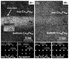
- FIG. 7 The figure which shows the HAADF-STEM image and the electron diffraction pattern of the sample of Example 7 and Example 3
- (a) and (b) in a figure are figures which show the HAADF-STEM image of Example 7 and Example 3, respectively.
- ((C), (d) and (e), (f) in the figure are diagrams showing electron diffraction patterns of Example 7 and Example 3, respectively.) Shows a HAADF-STEM images taken from different crystallization zone axis for the samples of Example 3 (in Fig. (A) is, Co 50 Fe 50 when rotated to 45 ° clockwise from FIG.
- FIG 9 (b) [100] is a diagram illustrating a HAADF-STEM images taken from the zone axis, (b) in the figure, Co 50 Fe 50 when rotated in 45 ° counterclockwise from FIG 9 (b) [010] zone axis It is a figure showing a HAADF-STEM image taken from the above.)
- the HAADF-STEM image, the inverse Fourier transform (IFFT) image, and the electron diffraction pattern of Cu layers having different thicknesses in the sample of Example 3 ((a) and (c) and (d) in the figure are respectively, It is a figure which shows a HAADF-STEM image with a thickness of 2.1 nm, and an electron diffraction pattern, and (b), (e), and (f) in the figure respectively are HAADF-STEM images with a thickness of 4.3 nm.
- FIG. 7 is a diagram showing an electron diffraction pattern.
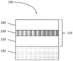
- FIG. 1 is a diagram showing a magnetoresistive effect element of the present invention.
- the magnetoresistive effect element 100 of the present invention includes a magnetoresistive effect film 110.
- a magnetoresistive effect film 110 includes at least a pair of ferromagnetic layers 120 and 140 and a nonmagnetic layer 130 located therebetween. Equipped with. With such a structure, the magnetoresistive effect element 100 of the present invention exhibits a giant magnetoresistive effect (GMR).
- FIG. 1 shows a magnetoresistive effect element 100 including a substrate 150 and a magnetoresistive effect film 110 formed thereon.
- each of the ferromagnetic layers 120 and 140 has a body-centered cubic (bcc) crystal structure and is represented by the general formula Co 100-p Fe p (where the parameter p is 0 ⁇ p ⁇ 75 is satisfied, and p in each of the ferroelectric layers 120 and 140 may be the same or different). Since, for the sake of simplicity, it referred to "the layer represented by Co 100-p Fe p" and "Co 100-p Fe p layer".
- the fcc crystal structure usually becomes a bcc crystal structure and can be stabilized.
- the ferromagnetic layers 120 and 140 may be Co 100-p Fe p layers having the same composition, or may have different compositions. If the composition is the same, the target does not need to be replaced and the manufacturing process is simplified, which is preferable. If the composition is different, a magnetization antiparallel state due to a difference in coercive force may be obtained, which is preferable.
- the parameter p preferably satisfies 0 ⁇ p ⁇ 70, and more preferably 0 ⁇ p ⁇ 65. As a result, the band structure is further matched, and the MR ratio can be further improved.
- the thickness of the ferromagnetic layers 120 and 140 is not particularly limited, but illustratively has a thickness in the range of 1.5 nm to 15 nm. If the thickness is in this range, the ferromagnetic layers 120 and 140 can be manufactured with good control by physical vapor deposition or chemical vapor deposition.
- the nonmagnetic layer 130 is a layer made of Cu having a body-centered cubic (bcc) crystal structure (hereinafter, referred to as a Cu layer for simplicity).
- bcc body-centered cubic
- fcc face-centered cubic
- the inventors of the present invention have found that a Co 100-p Fe p layer (0 ⁇ 0) having the above-described bcc crystal structure is obtained. It was found that the crystal structure of the Cu layer sandwiched between the ferromagnetic layers is p.ltoreq.75) and has a bcc crystal structure. Even more surprisingly, the present inventors have found that the use of a Cu layer having a bcc crystal structure as the nonmagnetic layer 130 causes the band structure to match the ferromagnetic layers 120 and 140 described above. ..
- the thickness of the nonmagnetic layer 130 is not particularly limited as long as it has a bcc crystal structure, but preferably has a range of 1.5 nm or more and 5 nm or less. Within this range, the nonmagnetic layer 130 can be manufactured with good controllability by physical vapor deposition or chemical vapor deposition while maintaining the bcc crystal structure, and at the same time, it becomes a continuous film, so that it is a ferromagnetic layer. The magnetic coupling that aligns the magnetizations between 120 and 140 in the parallel direction does not appear. More preferably, the thickness of the nonmagnetic layer 130 is in the range of 1.8 nm or more and 3 nm or less.
- the thickness of the nonmagnetic layer 130 is in the range of 1.8 nm or more and 2.5 nm or less. Within this range, the bcc crystal structure of the nonmagnetic layer 130 is stabilized, and the interface between the nonmagnetic layer 130 and the ferromagnetic layers 120 and 140 is well lattice-matched, so that the MR ratio can be improved.
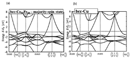
- FIG. 2 shows the band structure obtained from the first principle calculation.
- Bcc-Cu are very similar to the electron band structure. That is, since bcc-Co 100-p Fe p and bcc-Cu have the same band structure of electrons, they transport majority spin electrons at the interface like different substances though they are different substances. be able to.
- each of the ferromagnetic layers 120, 140 and the non-magnetic layer 130 is a single crystal (001) layer or is preferentially oriented in the (001) crystal plane.
- the interfaces of the ferromagnetic layers 120, 140 and the non-magnetic layer 130 are favorably lattice-matched, which promotes the matching effect of the band structure and allows the spin electrons to pass through without being scattered at the interfaces. The ratio can be improved.
- each of the ferromagnetic layers 120 and 140 and the nonmagnetic layer 130 is aligned with the crystal plane of the substrate 150 and is a single crystal-like (epitaxial film).
- a single crystal-like (epitaxial film) Is intended to be. Whether or not it is such an epitaxial film can be determined by X-ray diffraction, a transmission electron microscope (TEM), or the like.
- the preferential orientation to the (001) crystal plane means that a diffraction peak from a (001) plane of a body-centered cubic (bcc) crystal structure in a ⁇ -2 ⁇ scan of an X-ray diffraction method. It is intended that the intensity is higher than the diffraction peaks from other crystal planes, or that only the diffraction peaks from the (001) plane are observed.
- the magnetoresistive film 110 may be located on the substrate 150, in which case the substrate is preferably a glass substrate, an alumina substrate, a Si single crystal with or without a thermal oxide film, It is selected from the group consisting of MgO single crystal, sapphire single crystal, SrTiO 3 single crystal, MgAl 2 O 4 single crystal and TiO 2 single crystal.
- the substrate is preferably a glass substrate, an alumina substrate, a Si single crystal with or without a thermal oxide film, It is selected from the group consisting of MgO single crystal, sapphire single crystal, SrTiO 3 single crystal, MgAl 2 O 4 single crystal and TiO 2 single crystal.
- each of the ferromagnetic layers 120 and 140 and the nonmagnetic layer 130 grows epitaxially (is a single crystal (001) layer) or has priority over the (001) crystal plane.
- a crystal plane that is oriented may be selected. For example, when MgO single crystal is selected, the MgO(001) plane
- the substrate 150 having a bcc crystal structure may be positively adopted.
- the Co 100-p Fe p layer (0 ⁇ p ⁇ 20) changes from the fcc or hcp crystal structure to the bcc crystal structure and is stabilized.
- the substrate 150 may further include a buffer layer (not shown).
- a buffer layer (not shown).
- the substrate 150 is epitaxially grown (single crystal (001) layer) or preferentially oriented to the (001) crystal plane.
- Examples of such a buffer layer include Mg 1-x Ti x O (0 ⁇ x ⁇ 0.8), Cr, and TiN.
- the bcc crystal structure is used. It is preferable to positively adopt a buffer layer having for such a buffer layer, Co 100-p Fe p (20 ⁇ p ⁇ 100), Ni 100-p Fe p (70 ⁇ p ⁇ 100), or the like can be adopted. According to the state diagram, Co 100-p Fe p (20 ⁇ p ⁇ 100) has a bcc crystal structure, so that a Co 100-p Fe p layer (0 ⁇ p ⁇ 20) should be formed on it. For example, the crystal structure of fcc or hcp changes to the crystal structure of bcc and is stabilized.
- the ferromagnetic layer 140 is located on the nonmagnetic layer 130 which is a layer made of Cu having a bcc crystal structure, as will be described later, the nonmagnetic layer 130 serves as a buffer layer and has a bcc crystal structure.
- the Co 100-p Fe p layer (0 ⁇ p ⁇ 75) is stabilized.
- the magnetizations of the ferromagnetic layers 120 and 140 need to be oriented in a completely antiparallel state in a certain magnetic field region. Therefore, materials having different coercive forces may be used for the ferromagnetic layers 120 and 140, an exchange bias may be applied to the structure including the antiferromagnetic layer 320 shown in FIG. 140 may obtain an antiferromagnetic interlayer exchange interaction through the nonmagnetic layer 130.
- the magnetoresistive effect film 110 of the present invention is adopted, interlayer exchange interaction can be obtained. If the laminated structure shown in FIG. 1 is repeated and the artificial lattice structure shown in FIG. 4 is used, antiparallel coupling continues in the stacking direction indefinitely, and the magnetizations of the adjacent ferromagnetic layers are always antiparallel. Therefore, a large MR ratio can be expected.
- the composition of the Co 100-p Fe p layers forming the respective ferromagnetic layers may be controlled (that is, the value of the parameter p).
- the magnetoresistive film 110 has a set of multilayer structure including a pair of ferromagnetic layers 120 and 140 and a non-magnetic layer 130 located between them. Good.
- each of the two or more multilayer structures is separated by an insulating layer (barrier layer).
- the insulating layer include MgO and AlO.
- the thickness of the insulating layer is preferably 0.2 nm or more and 3 nm or less.
- the magnetoresistive effect film 110 may further include a cap layer (not shown) on the ferromagnetic layer 140.
- the cap layer may function as a protective layer on the surface of the magnetoresistive effect film 110.
- examples of such a cap layer include tantalum (Ta), gold (Au), aluminum (Al), ruthenium (Ru), platinum (Pt), and the like.
- the thickness of the cap layer is preferably 0.5 nm or more and 2 nm or less.
- FIG. 3 is a diagram showing a magnetoresistive effect element 300 which is another embodiment of the present invention.
- the magnetoresistive effect film 310 includes an antiferromagnetic layer 320 magnetically coupled to one of the pair of ferromagnetic layers 120 and 140, that is, the antiferromagnetic layer 320 of FIG. Different from the magnetoresistive effect element 100.
- the same elements as those in FIG. 1 are denoted by the same reference numerals and the description thereof will be omitted.
- the magnetoresistive film 310 is called a spin valve
- the ferromagnetic layer 120 serves as a free layer
- the ferromagnetic layer 140 and the antiferromagnetic layer 320 function as a pinned layer
- the giant magnetoresistive effect can be exhibited by changing the direction of.
- an antiferromagnetic layer 320 an antiferromagnetic layer generally used in the art is adopted, but it is illustratively selected from the group consisting of an IrMn layer, a FeMn layer, a PtMn layer and a CoO layer. To be done.
- the thickness of the antiferromagnetic layer 320 is preferably 1 nm or more and 10 nm or less.
- the magnetoresistive effect film 310 has a multilayer structure of one set of the ferromagnetic layer 120, the nonmagnetic layer 130, the ferromagnetic layer 140, and the antiferromagnetic layer 320, but like the magnetoresistive effect film 110, Two or more such multilayer structures may be provided. In this case, each of the two or more multi-layer structures is separated by an insulating layer. With such a structure, the MR ratio can be increased.
- the insulating layer is as described above.
- the magnetoresistive effect film 310 has two or more multilayer structures of the ferromagnetic layer 120, the nonmagnetic layer 130, the ferromagnetic layer 140, and the antiferromagnetic layer 320 so as to share the ferromagnetic layer 120 that is a free layer. You may. Such a structure is called a dual spin valve type magnetoresistive effect element.
- the magnetoresistive effect film 310 of FIG. 3 may include a cap layer (not shown) on the antiferromagnetic layer 320, like the magnetoresistive effect film 110 of FIG.
- the cap layer is as described above.
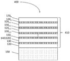
- FIG. 4 is a diagram showing a magnetoresistive effect element 400 which is still another embodiment of the present invention.
- the magnetoresistive effect film 410 has a multi-layered structure including a pair of ferromagnetic layers 120 and 140 and a non-magnetic layer 130 located therebetween, as well as the ferromagnetic layers 120 1 to n. It differs from the magnetoresistive effect element 100 of FIG. 1 and the magnetoresistive effect element 300 of FIG. 3 in that it has an artificial lattice structure in which layers 130 1 to n are alternately and repeatedly laminated.
- elements similar to those in FIG. 1 are assigned the same reference numerals and explanations thereof are omitted.
- the magnetoresistive effect film 410 can exhibit a giant magnetoresistive effect.
- the number of repetitions n in this case is not particularly limited, but is illustratively in the range of 2 or more and 100 or less.
- the magnetoresistive effect film 410 of FIG. 4 is similar to the magnetoresistive effect film 110 of FIG. 1 and the magnetoresistive effect film 310 of FIG. 3, and a cap layer (not shown) or an antiferromagnetic layer on the ferromagnetic layer 120 n. (Not shown) may be provided.
- the cap layer and the antiferromagnetic layer are as described above.
- the ferromagnetic layers 120 1 to 120 n are coupled to the magnetizations of the ferromagnetic layers adjacent to each other with the nonmagnetic layer 130 in between, and antiparallel interlayer magnetic coupling (interlayer exchange) is performed. (Interaction), and the antiparallel state of the magnetization is obtained by this, so that the MR ratio can be increased.
- the magnetoresistive effect elements 100, 300, 400 of the present invention are used as a CIP (Current in Plane) type magnetoresistive effect element, in which a current flows in the in-plane direction of the magnetoresistive effect films 110, 310, 410, It is preferable because it exhibits a large MR ratio. However, even if the magnetic effect elements 100, 300, 400 of the present invention are used as a CPP (Current Perpendicular to Plane) type magnetoresistive effect element in which a current is passed in the stacking direction of the magnetoresistive effect films 110, 310, 410, no problem.
- CIP Current in Plane
- CPP Current Perpendicular to Plane
- the magnetoresistive effect films 110, 310, 410 may include a buffer layer, a reference layer, a barrier layer, etc., if necessary.
- An exemplary method of manufacturing the magnetoresistive effect element 100 of the present invention is as follows.
- the ferromagnetic layer 120, the nonmagnetic layer 130, and the ferromagnetic layer 140 are sequentially formed on the substrate 150.
- a buffer layer, a cap layer, a shield layer, a reference layer, a barrier layer, etc. may be formed.
- the antiferromagnetic layer 320 FIG. 3
- the magnetoresistive effect element 300 is manufactured, and if the ferromagnetic layer and the nonmagnetic layer are repeatedly laminated, the magnetoresistive effect element 400 is manufactured.
- these layers can be formed by a physical vapor deposition method or a chemical vapor deposition method, and a physical vapor deposition method typified by a sputtering method is preferably adopted. .. Further, after the film formation, physical or chemical etching or photolithography is performed and fine processing is performed to obtain a magnetoresistive effect element. See the examples below for exemplary manufacturing methods.
- FIG. 5 is a diagram showing a magnetic sensor of the present invention.
- the magnetic sensor 500 of the present invention includes a magneto-resistance effect element 100 A, 100 B as the magnetoresistive effect element 100 described in FIG. In FIG. 5, two magnetoresistive elements 100 A, 100 B are connected, the number of elements is not limited to two.
- the magnetic sensor 500 uses the magnetoresistive effect element 100 shown in FIG. 1, but instead of the magnetoresistive effect element 100 of FIG. 1, the magnetoresistive effect element 300 of FIG. 3 and the magnetoresistive effect element 400 of FIG. Alternatively, a combination of these may be used.
- a magnetic detection device may be realized.
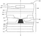
- FIG. 6A is a diagram showing a magnetic head in which the reproducing head and the recording head of the present invention are combined.
- 6B is a cross-sectional view taken along the line AA shown in FIG. 6A.
- the magnetic head 600 includes the reproducing head 610 and the recording head 620 of the present invention, and the structure of the air bearing surface is shown.
- the vertical direction of the paper surface is the moving direction of the magnetic recording medium (not shown), and the horizontal direction of the paper surface corresponds to the width direction of the tracks formed on the magnetic recording medium.
- the magnetic head 600 of FIG. 6B is in a state of a cross section in a plane direction perpendicular to the line AA.
- the reproducing head 610 of the present invention only needs to include at least the magnetoresistive effect element 100.
- the insulating layer 612, the lower shield layer 613, the lower gap insulating layer 614, and the magnetoresistive effect element are provided on the flat slider 611.
- the recording head 620 is provided on the reproducing head 610 via an insulating layer 621, and normally, on the side facing the lower magnetic pole 622 with the lower magnetic pole 622 and the recording gap layer 624 interposed therebetween, a track of a magnetic recording medium is usually formed. Is provided with an upper magnetic pole 625, which is covered with an insulating layer 623. Further, as shown in FIG. 6B, the recording head 620 includes a yoke that connects the lower magnetic pole 622 and the upper magnetic pole 625, and a coil 626 that winds the yoke.
- Materials such as an insulating layer, a shield layer, a yoke, a coil, a magnetic pole, a terminal, and a magnetic domain control layer, which are exemplarily shown in FIGS. 6A and 6B, are not particularly limited as long as they are commonly used in the field. Good.
- the magnetic head 600 records information on the opposing magnetic recording medium by the recording magnetic field leaking from the lower magnetic pole 622 and the upper magnetic pole 625 of the recording head 620, and the magnetic recording medium corresponding to the recorded information.
- the leakage magnetic field is detected by the magnetoresistive effect element 100 of the reproducing head 610 as a resistance change.
- a sense current for detecting a resistance change flows from the pair of terminal layers 616 in the in-plane direction of the magnetoresistive effect film of the magnetoresistive effect element 100, and is drawn out from the other terminal layer 616.
- the change in the leakage magnetic field from the magnetic recording medium is detected by the change in the electric resistance value of the magnetoresistive effect element 100 by the voltage across the magnetoresistive effect element 100 generated when the sense current is passed.
- FIG. 6A and FIG. 6B show the composite type magnetic head 600 including the reproducing head 610 and the recording head 620, it may be configured as a magnetic head including only the reproducing head 610.
- the magnetoresistive effect element 100 may of course use the magnetoresistive effect elements 300 and 400.
- FIG. 7 is a diagram showing a magnetic recording/reproducing apparatus of the present invention.
- the magnetic recording/reproducing apparatus 700 includes an actuator 720, an actuator arm 730 attached to the actuator 720, a head slider 740 attached to the tip of the actuator arm 730, and a magnetic recording medium 750 in a rectangular housing 710. ..
- At least the reproducing head 610 of the present invention described with reference to FIGS. 6A and 6B is attached to the head slider 740 that records and reproduces information stored in the magnetic recording medium 750.
- the magnetic recording medium 750 is rotated in the direction of the arrow by a motor that responds to a control signal from a control unit (not shown) of the drive device.
- a control unit not shown
- the magnetic recording medium 750 rotates, the medium facing surface of the head slider 740 is maintained at a predetermined flying height from the surface of the magnetic recording medium 750 or comes into contact with the surface.
- the reproducing head 610 using the above-described magnetoresistive effect element of the present invention since the reproducing head 610 using the above-described magnetoresistive effect element of the present invention is adopted, noise can be reduced and stable signal recording/reproducing can be performed.
- the magnetic recording medium 750 is not limited to the magnetic disk.
- Examples 1 to 9 In Examples 1 to 9, a Co 100-p Fe p layer was used as a ferromagnetic layer on a MgO(001) single crystal substrate or a c-Si(001) single crystal substrate with a thermal oxide film (SiOx). A Cu layer or an Ag layer was used as the magnetic layer to manufacture a magnetoresistive effect element.
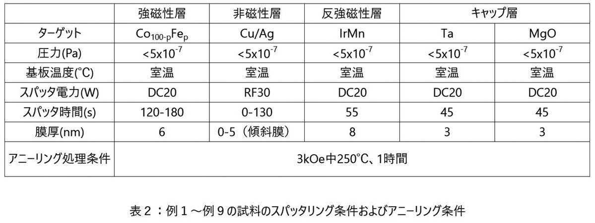
- Targets of various compositions of Co 100-p Fe p , Cu, Ag, IrMn, and Ta were set on a DC-RF magnetron sputter (Eiko Engineering Co., Ltd., model number ESA-0788), and the sputtering conditions shown in Table 2 were used. Sputtering was performed. Then, under the annealing conditions shown in Table 2, the samples of Examples 1 to 9 were heat-treated in a magnetic field to impart unidirectional magnetic anisotropy. The samples of Examples 1 to 9 were processed into a wire shape by photolithography. In addition, in preliminary experiments, it was confirmed from composition analysis that the composition of the target and the composition of the ferromagnetic layer were substantially the same, so in the present specification, the composition used for the target was obtained. It is treated as the composition of the ferromagnetic layer.
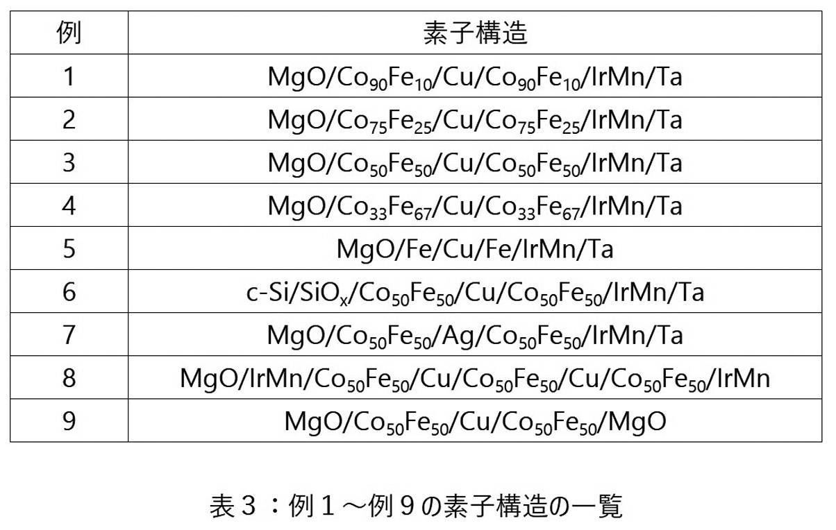
- Table 3 shows the structures of the samples of Examples 1 to 9 thus obtained.
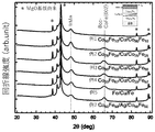
- X-ray diffraction was performed on the samples of Examples 1 to 9. The results are shown in Fig. 8. High-resolution observation of the samples of Examples 1 to 9 by high-angle scattering dark-field scanning transmission electron microscopy (HAADF-STEM method) using a transmission electron microscope (TEM, FEI, model number TITAN G2-200). Then, an electron diffraction pattern was obtained. The results are shown in FIGS. 9 to 11.
- the magnetic properties of the samples of Examples 1 to 9 were measured using the 4-probe method. Specifically, at room temperature (25° C.), an electric current is applied in the in-plane direction of the film, an external magnetic field is applied in a direction parallel to that direction, the change in resistance value at that time is measured, and the MR ratio is determined. It was Further, the samples of Examples 3 and 7 were examined for temperature dependence of MR ratio, resistance (R) and resistance change (dR). The bias voltage dependence of the MR ratio of the sample of Example 8 and the dependence of the resistance value on the external magnetic field of the sample of Example 9 were examined. The results are shown in FIGS. 12 to 19.
- FIG. 8 is a diagram showing XRD patterns of the samples of Examples 1 to 5 and 7.
- FIG. 9 is a diagram showing HAADF-STEM images and electron diffraction patterns of the samples of Examples 7 and 3.
- FIG. 10 is a diagram showing a HAADF-STEM image of the sample of Example 3 taken from a zone axis different from that of FIG. 9.
- FIG. 11 is a diagram showing a HAADF-STEM image, an inverse Fourier transform (IFFT) image, and an electron diffraction pattern of Cu layers having different thicknesses in the sample of Example 3.
- IFFT inverse Fourier transform
- FIGS. 10(a) and 10(b) are HAADF images taken from Co 50 Fe 50 [100] and [010] crystal band axes when rotated clockwise and counterclockwise by 45° from FIG. 9(b), respectively.
- FIG. 7 is a view showing a STEM image. According to FIGS. 10( a) and 10 (b ), both images are similar to each other, and there is no visible lattice strain at the interface between the Co 50 Fe 50 layer and the Cu layer.
- Cu has a crystal structure of fcc
- the 45° clockwise image and the 45° counterclockwise image are different from each other, and lattice distortion occurs at the interface between the Co 50 Fe 50 layer and the Cu layer.
- the 45° clockwise image and the 45° counterclockwise image are similar to each other, and lattice strain cannot be confirmed at the interface. Therefore, Cu is a crystalline structure of Co 50 Fe 50 .
- it has a bcc crystal structure, and it can be said that the Co 50 Fe 50 layer and the Cu layer are both single crystal (001) layers.
- Example 5 The sample of Example 5 is B. Heinrich et al., Phys. Rev. Lett. , Vol. 64, No. Similar to the report of 6, 1990, both the Fe layer and the Cu layer had a bcc crystal structure and were single crystal (001) layers, but the Co 100-p Fe p layer and the Cu layer were also the same. It should be noted that the inventors of the present application first confirmed from experiments that the relationship of
- FIGS. 11A and 11B show atomic resolution HAADF-STEM images of the cross section of the sample of Example 3 in which the Cu layer thicknesses are 2.1 nm and 4.3 nm, respectively.
- 11(c), (d) and (e), (f) show the electron diffraction patterns of the sample of Example 3 in which the Cu layer thicknesses are 2.1 nm and 4.3 nm, respectively.
- FIGS. 11A, 11C and 11D are the same as FIGS. 9B, 9E and 9F.
- the thickness of the Cu layer when the thickness of the Cu layer was increased, a slight lattice strain was confirmed at the interface between the Cu layer and the Co 50 Fe 50 layer, but according to FIGS. 11(e) and 11(f).
- the Cu layer maintained the bcc crystal structure.
- the upper limit of the thickness of the Cu layer is preferably 5 nm in order that the Cu layer maintains the bcc crystal structure and has a good lattice matching at the interface.
- the lower limit if the Cu layer can be formed flat and uniform even if the thickness is 1 nm or less, there is no particular limitation to maintain the bcc crystal structure.
- the thickness is preferably 1.5 nm or more.
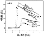
- FIG. 12 is a diagram showing the dependence of the MR ratio of the samples of Examples 1 to 5 on the thickness of the Cu layer.
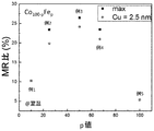
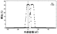
- FIG. 13 is a diagram showing the p-value dependence of the MR ratio of Co 100-p Fe p .
- the MR ratio increases as the thickness of the Cu layer decreases, and the thickness of the Cu layer further decreases. The ratio disappeared.
- the MR ratios of the samples of Examples 2 to 4 are significantly higher than those of the samples of Examples 1 and 5.
- the sample of Example 3 showed a maximum MR ratio of greater than 25%.
- the Cu layer when the Cu layer was 1.5 nm or less, the ferromagnetic layers were magnetically coupled and the MR ratio disappeared. This is because the Cu layer has a high MR ratio by improving the film quality and flatness. Think that you can maintain.
- the Cu layer depending on the p-value of the Co 100-p Fe p layer, the Cu layer preferably has a remarkable improvement in thickness of 1.5 nm or more, and has a special film quality control (eg Cu It was shown that a high MR ratio can be maintained without the need of optimizing the film formation rate and the substrate temperature at the time of forming the layer.
- Example 1 exhibited the fcc crystal structure as described with reference to FIG. 8.
- Co 100-p Fe p (20 ⁇ p ⁇ 100) having the bcc crystal structure on the substrate was used.
- a buffer layer such as the above is provided, both the ferromagnetic layer and the nonmagnetic layer have a bcc crystal structure, and the magnetoresistive effect element preferentially oriented to the single crystal (001) layer or the (001) crystal plane (for example, It is suggested that MgO/Co 100-p Fe p /Co 90 Fe 10 /Cu/Co 90 Fe 10 /IrMn/Ta etc.) can be provided.
- FIG. 13 shows the MR ratio values (indicated by circles) of the samples of Examples 1 to 5 in which the thickness of the Cu layer is 2.5 nm and the maximum values of the MR ratios of the samples of Examples 1 to 5 (squares). Are shown).
- the samples of Examples 2 to 4 all had a high MR ratio of more than 20% or about 20%.
- the samples of Examples 1 and 5 had a small MR ratio of 10% or less as in the conventional case.
- the p value of the Co 100-p Fe p layer that is a binary alloy is 20 or more and 75 or less, preferably 22 or more and 70 or less, more preferably 25 or more and 65 or less, and still more preferably 40 or more. It was shown to be 60 or less.
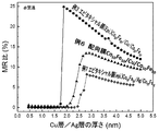
- FIG. 14 is a diagram showing the dependence of the MR ratios of the samples of Examples 3, 6 and 7 on the thickness of the Cu layer/Ag layer.
- the dependence of the MR ratio of the sample of Example 3 on the thickness of the Cu layer is the same as that of FIG. According to FIG. 14, the MR ratio of the sample of Example 6 was smaller than that of the sample of Example 3, but was larger than that of the sample of Example 7. From this, in the sample of Example 6, the Co 100-p Fe p layer and the Cu layer are preferentially oriented in the (001) crystal plane, and as a result, function as a magnetoresistive film capable of obtaining a large MR ratio. Is suggested.
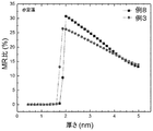
- FIG. 15 is a diagram showing the dependence of the MR ratios of the samples of Examples 3 and 8 on the thickness of the Cu layer.
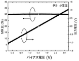
- FIG. 16 is a diagram showing the MR ratio of the sample of Example 8 and the bias voltage dependence of the output voltage.
- the MR ratio of the sample of Example 8 was larger than that of the sample of Example 3. From this, the magnetoresistance obtained by repeating two or more of the ferromagnetic layer (bcc-Co 100-p Fe p ) and the non-magnetic layer (bcc-Cu) preferentially oriented to the single crystal (001) layer or the (001) plane.
- a magnetoresistive effect element having an effect film has a larger MR ratio and has been found to be advantageous.
- the magnetoresistive effect element of the present invention is advantageous in obtaining a high voltage output due to the magnetoresistive effect.
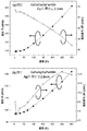
- FIG. 17 is a diagram showing the temperature dependence of the MR ratio of the samples of Examples 3 and 7.
- FIG. 18 is a diagram showing the temperature dependence of resistance (R) and resistance change (dR) of the samples of Examples 3 and 7.
- the MR ratio of the sample of Example 3 further increased as the temperature decreased, and a maximum MR ratio of 40% was obtained at 10K.
- the sample of Example 7 maintained a small MR ratio of about 10% and did not change even when the temperature was lowered.
- FIG. 18 the temperature dependence of the MR ratio obtained in FIG. 17 is shown separately for the resistance R and the resistance change dR. Focusing on the temperature dependence of the resistance R, both the sample of Example 3 and the sample of Example 7 showed similar temperature dependence. However, focusing on the resistance change dR, the resistance change dR of the sample of Example 3 increased as the temperature decreased, whereas that of the sample of Example 7 decreased as the temperature decreased. This indicates that the spin asymmetry of the interface scattering increased and the MR ratio improved when the mean free path of the electrons became longer at low temperature, and the Co 100-p Fe p in the sample of Example 3 was improved. It is suggested that the band matching at the interface of the majority spin electrons between the layer and the Cu layer is higher than that between the Co 100-p Fe p layer and the Ag layer in the sample of Example 7.
- FIG. 19 is a diagram showing the external magnetic field dependence of the MR ratio of the sample of Example 9.
- Example 9 since the sample of Example 9 uses Co 50 Fe 50 having the same film thickness and the same composition on the upper and lower sides, a coercive force difference does not occur, and even if an exchange bias due to an antiferromagnetic material is applied. However, a clear antiparallel state was realized with zero external magnetic field, and the MR ratio was as large as 31%. This indicates that in the sample of Example 9, the magnetization of the Co 50 Fe 50 layer was in the antiparallel state due to the interlayer exchange interaction via Cu.
- an artificial lattice in which a plurality of these layers are stacked, a magnetized state in which adjacent Co 50 Fe 50 layers are alternately oriented in antiparallel is realized, and a magnetoresistive effect element having a larger MR ratio is expected. it can.
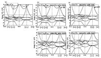
- FIG. 20 is a diagram showing band structures of bcc-Cu, bcc-Co 50 Fe 50, and bcc-Fe by first-principles calculation.
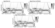
- FIG. 21 is a diagram showing band structures of (a) bcc-Co, (b) bcc-Co 75 Fe 25, and (c) bcc-Co 25 Fe 75 by first-principles calculation.
- FIGS. 20B and 20C show a band structure of bcc-Co 50 Fe 50 in a majority spin state and a minority spin state, respectively.
- 20(d) and 20(e) show band structures of bcc-Fe in the majority spin state and the minority spin state, respectively.
- the band dispersion of bcc-Cu is very similar to the majority spin state of bcc-Co 50 Fe 50. And the band structure matches well. 20A and 20C are compared, the band dispersion of bcc-Cu is different from the minority spin state of bcc-Co 50 Fe 50 . Further, comparing FIG. 20(a) with FIGS. 21(a) to 21(c), the band dispersions of bcc-Cu are bcc-Co, bcc-Co 75 Fe 25 , and bcc-Co 25 Fe 75 . It is very similar to the majority spin state, and the band structure is well matched.
- the up-spin electrons can move more easily between the bcc-Co 100-p Fe p layer (where 0 ⁇ p ⁇ 75) and the bcc-Cu layer than the down-spin electrons. .. Due to such a high spin asymmetry, a large MR ratio can be obtained.
- the present inventors have proposed a ferromagnetic layer having a body-centered cubic (bcc) crystal structure, which is a layer represented by the general formula Co 100-p Fe p (the parameter p satisfies 0 ⁇ p ⁇ 75), and It has been found that a nonmagnetic layer, which is a layer made of Cu and has a body-centered cubic (bcc) crystal structure, shows good band structure matching as shown in FIGS.
- bcc body-centered cubic
- the magnetoresistive effect element of the present invention exhibits a high MR ratio even when used in a CIP type, it is applied to a magnetic sensor, a reproducing head and a magnetic recording/reproducing apparatus having high sensitivity to a magnetic field due to such a high MR ratio. ..
- Magnetic sensor 600 magnetic head 610 reproducing head 620 recording head 611 sliders 612, 621, 623 insulating layer 613 lower shield layer 614 lower gap insulating layer 615 magnetic domain control layer 616 pair of terminal layers 617 upper gap insulating layer 618 upper shield layer 622 lower magnetic pole 624 recording Gap layer 625 Upper magnetic pole 626 Coil 700 Magnetic recording/reproducing device 710 Housing 720 Actuator 730 Actuator arm 740 Head slider 750 Magnetic recording medium
Landscapes
- Physics & Mathematics (AREA)
- Engineering & Computer Science (AREA)
- Manufacturing & Machinery (AREA)
- General Physics & Mathematics (AREA)
- Condensed Matter Physics & Semiconductors (AREA)
- Power Engineering (AREA)
- Environmental & Geological Engineering (AREA)
- Toxicology (AREA)
- Health & Medical Sciences (AREA)
- Chemical & Material Sciences (AREA)
- Crystallography & Structural Chemistry (AREA)
- Hall/Mr Elements (AREA)
- Magnetic Heads (AREA)
- Thin Magnetic Films (AREA)
Abstract
大きな磁気抵抗変化率(MR比)を有する磁気抵抗効果素子、ならびに、その大きなMR比による磁場に対する高い感度を有する磁気センサ、再生ヘッドおよび磁気記録再生装置を提供することを目的とする。 本発明の磁気抵抗効果膜を備えた磁気抵抗効果素子は、磁気抵抗効果膜は、少なくとも、一対の強磁性層と、一対の強磁性層の間に位置する非磁性層とを備え、一対の強磁性層のそれぞれは、体心立方(bcc)の結晶構造を有し、一般式Co100-pFepで表される層(パラメータpは、0≦p≦75を満たし、一対の強磁性層のそれぞれにおけるpは、同一または別異である)であり、非磁性層は、体心立方(bcc)の結晶構造を有し、Cuからなる層であり、強磁性層、および、非磁性層のそれぞれは、単結晶(001)層であるか、または、(001)結晶面が優先配向している。
Description
本発明は、磁気抵抗効果素子、磁気センサ、再生ヘッドおよび磁気記録再生装置に関する。
一対の強磁性層と、それに挟まれた非磁性層との多層膜を有する磁気抵抗効果素子が知られている。このような磁気抵抗効果素子は、多層膜の面内方向に電流を流すCIP(Current in Plane)型として、あるいは、多層膜の積層方向に電流を流すCPP(Current Perpendicular to Plane)型として使用される。
CIP型磁気抵抗効果素子は、トンネル磁気抵抗効果素子に比べてノイズが小さいという利点があるが、磁気抵抗変化率(MR比)が小さく、磁気センサとしての高感度ためにはMR比の増大が求められる。
このようなCIP型磁気抵抗効果素子として、強磁性層にCo90Fe10を、非磁性層にCuを用いた磁気抵抗効果素子が知られている(例えば、特許文献1を参照)。特許文献1の実施例1によれば、サファイア基板C面上にCo90Fe10膜、Cu膜、Co90Fe10膜、FeMn膜、Ti膜を順次成膜したCo90Fe10/Cu/Co90Fe10/FeMn/Tiなるスピンバルブ構造を有する磁気抵抗効果素子において、Co90Fe10層がfcc相(111)面配向をしており、10%の磁気抵抗変化率(MR比)を示した。しかしながら、磁気センサとしての感度向上のためには、さらなるMR比の向上が求められている。
近年、MR比が25%となるCIP型磁気抵抗効果素子が開発された(例えば、非特許文献1を参照)。非特許文献1によれば、シリコン熱酸化膜を基板としたSiOx/NiFeCr/CoFeOx/Co90Fe10/Cu/Co90Fe10/AlOのCIP型磁気抵抗効果素子は、25%を超えるMR比を示す。しかしながら、強磁性層以外にNiFeCrやCoFeOx等の層を設ける必要があり、プロセスが煩雑になるのに加え、CoFeOx層におけるスペキュラー反射を利用しMR比を向上させているため、多層膜化によるMR比の向上は得られないという問題がある。
また、このような磁気抵抗効果素子において、層の界面におけるスピン電子の透過率がMR比に影響することが報告されている(例えば、非特許文献2を参照)。非特許文献2の「Chapter 2、2.3.3 CIP transport properties」は、強磁性層のマジョリティスピンを有する電子のバンド構造と、非磁性層の電子のバンド構造との間の良好なマッチングにより、マジョリティスピン電子の透過率が増大し、MR比が向上することを報告する。しかしながら、上述の特許文献1や非特許文献1において、CoとFeとからなる二元系合金の強磁性層と、Cuからなる非磁性層との間の電子のバンド構造のマッチングについては何ら報告がない。
このように、CoとFeとからなる二元系合金の強磁性層およびCuからなる非磁性層を用い、とりわけ、面方向に電流を流した際に、大きなMR比が得られる磁気抵抗効果素子が開発されることが望まれる。
M.Seigler,IEEE Transaction on Magnetics,Vol.43,No.2,651-656,2007
M.Johnson編集,12月2日2004年,「Magnetoelectronics」1stEdition,Chapter 2、2.3.3 CIP transport properties
以上から、本発明の課題は、大きな磁気抵抗変化率(MR比)を有する磁気抵抗効果素子、ならびに、その大きなMR比による磁場に対する高い感度を有する磁気センサ、再生ヘッドおよび磁気記録再生装置を提供することである。
本発明による磁気抵抗効果膜を備えた磁気抵抗効果素子は、前記磁気抵抗効果膜は、少なくとも、一対の強磁性層と、前記一対の強磁性層の間に位置する非磁性層とを備え、前記一対の強磁性層のそれぞれは、体心立方(bcc)の結晶構造を有し、一般式Co100-pFepで表される層(パラメータpは、0≦p≦75を満たし、前記一対の強磁性層のそれぞれにおけるpは、同一または別異である)であり、前記非磁性層は、体心立方(bcc)の結晶構造を有し、Cuからなる層であり、前記一対の強磁性層、および、前記非磁性層のそれぞれは、単結晶(001)層であるか、または、(001)結晶面に優先配向しており、これにより上記課題を解決する。
前記パラメータpは、0≦p≦70を満たしてもよい。
前記パラメータpは、p=0または20≦p≦75を満たしてもよい。
前記パラメータpは、p=0または22≦p≦70を満たしてもよい。
前記パラメータpは、0≦p≦65を満たしてもよい。
前記パラメータpは、p=0または25≦p≦65を満たしてもよい。
前記非磁性層は、1.5nm以上5nm以下の範囲の厚さを有してもよい。
前記一対の強磁性層のそれぞれは、1.5nm以上15nm以下の範囲の厚さを有してもよい。
前記磁気抵抗効果膜は、前記一対の強磁性層のうち一方と磁気的に結合する反強磁性層をさらに備えてもよい。
前記反強磁性層は、IrMn層、FeMn層、PtMn層およびCoO層からなる群から選択されてもよい。
前記磁気抵抗効果膜は、前記一対の強磁性層と、前記一対の強磁性層の間に位置する前記非磁性層とからなる多層構造を2以上有し、前記2以上の多層構造のそれぞれは絶縁層によって分離していてもよい。
前記磁気抵抗効果膜は、前記強磁性層と前記非磁性層とが繰り返し積層された人工格子構造であってもよい。
前記強磁性層のそれぞれは、異なる保磁力を有してもよい。
前記前記磁気抵抗効果膜は基板上に位置し、前記基板は、ガラス基板、アルミナ基板、熱酸化膜を有する/有しないSi単結晶、MgO単結晶、サファイア単結晶、SrTiO3単結晶、MgAl2O4単結晶およびTiO2単結晶からなる群から選択されてもよい。
前記基板は、バッファ層をさらに備えてもよい。
前記磁気抵抗効果膜は、キャップ層をさらに備えてもよい。
前記磁気抵抗効果素子は、前記磁気抵抗効果膜の面内方向に電流を流すCIP(Current in Plane)型、または、前記磁気抵抗効果膜の積層方向に電流を流すCPP(Cuttent Perpendicular to Plane)型であってもよい。
本発明による磁気抵抗効果素子を備えた磁気センサは、前記磁気抵抗効果素子が上述の磁気抵抗効果素子であり、これにより上記課題を解決する。
本発明による磁気抵抗効果素子を備えた磁気記録再生装置用の再生ヘッドは、前記磁気抵抗効果素子が上述の磁気抵抗効果素子であり、これにより上記課題を解決する。
本発明による再生ヘッドを備えた磁気記録再生装置は、前記再生ヘッドが上述の再生ヘッドであり、これにより上記課題を解決する。
前記磁気記録再生装置は記録ヘッドをさらに備えてもよい。
本発明の磁気抵抗効果素子は、少なくとも、一対の強磁性層と、一対の強磁性層の間に位置する非磁性層とを備えた磁気抵抗効果膜を備えるので、巨大磁気抵抗効果が期待される。また、一対の強磁性層のそれぞれは、体心立方(bcc)の結晶構造を有し、一般式Co100-pFepで表される層(パラメータpは、0≦p≦75を満たし、一対の強磁性層のそれぞれにおけるpは、同一または別異である)であり、非磁性層は、体心立方(bcc)の結晶構造を有し、Cuからなる層である。これにより、強磁性層のマジョリティスピンを有する電子のバンド構造と、非磁性層の電子のバンド構造とは、フェルミ準位(E-EF=0)において、良好にマッチングする。また、これらの強磁性層、および、非磁性層のそれぞれは、単結晶(001)層であるか、または、(001)結晶面に優先配向している。これにより、強磁性層と非磁性層との間の界面は良好に整合するため、界面においてスピン電子の透過率が増大し、MR比が顕著に向上する。
このような効果は、CIP型磁気抵抗効果素子に特に有効であるが、CIP型以外にもCPP型でも同様の効果が期待される。また、本発明の磁気抵抗効果素子は、磁気センサ、再生ヘッドおよび磁気記録再生装置に適用される。
以下、図面を参照しながら本発明の実施の形態を説明する。なお、同様の要素には同様の番号を付し、その説明を省略する。
(実施の形態1)
実施の形態1では、本発明の磁気抵抗効果素子およびその製造方法について説明する。
(実施の形態1)
実施の形態1では、本発明の磁気抵抗効果素子およびその製造方法について説明する。
図1は、本発明の磁気抵抗効果素子を示す図である。
本発明の磁気抵抗効果素子100は、磁気抵抗効果膜110を備えるが、このような磁気抵抗効果膜110は、少なくとも、一対の強磁性層120、140と、その間に位置する非磁性層130とを備える。このような構造により、本発明の磁気抵抗効果素子100は巨大磁気抵抗効果(GMR)を示す。図1では、基板150と、その上に形成された磁気抵抗効果膜110とを備える磁気抵抗効果素子100を示す。
ここで、強磁性層120、140のそれぞれは、体心立方(bcc)の結晶構造を有し、一般式Co100-pFepで表される層(ここで、パラメータpは、0≦p≦75を満たし、強誘電層120、140のそれぞれにおけるpは、同一であってもよいし、別異であってもよい)である。以降では、簡単のため、「Co100-pFepで表される層」を「Co100-pFep層」と称する。
CoとFeとの二元系合金において、Co100-pFep層(20≦p≦75)であれば、状態図からbccの結晶構造を取ることが知られている。
一方、Co100-pFep層(0<p<20)においては、状態図からbccの結晶構造を維持できない場合があるが、bccの結晶構造を有するバッファ層(下地層)あるいはbccの結晶構造を有する基板上にこれらの層を成長させた場合、通常fccの結晶構造が、bccの結晶構造となり安定化し得る。
また、pが0の場合、Co100-pFep層はCo層となるが、Shinji Yuasaら,Applied Physics Letters 89,04505(2006)によると、bccの結晶構造を有するバッファ層(下地層)あるいはbccの結晶構造を有する基板上に成長させた場合、通常、六方最密充填構造(hcp)が安定なCoが、bccの結晶構造となることが示されている。
さらに、本願発明者らは、p=0のCo、ならびに、0<p≦75を満たすCo100-pFepのバンド構造が、bccの結晶構造を有せば、後述するbccの結晶構造を有するCuのバンド構造と、フェルミ準位(E-EF=0)において良好にマッチングすることを見出し、bccの結晶構造を有するCo100-pFep層(0≦p≦75)を強磁性層120、140に、bccの結晶構造を有するCuからなる層を非磁性層130に採用し、MR比が向上した磁気抵抗効果素子を提供できる。後述するように、pが75を超えると、バンド構造がマッチングしない場合があるため、pの上限は75が妥当である。
また、上述したように、強磁性層120、140は、それぞれ、同じ組成を有するCo100-pFep層であってもよいし、別の組成を有していてもよい。同じ組成であれば、ターゲットの交換が不要であるため、製造プロセスが簡略化されるので好ましい。異なる組成であれば、保磁力差による磁化反平行状態が得られる可能性があるため、好ましい。
バンド構造のマッチングの観点から、パラメータpは、好ましくは、0≦p≦70、なお好ましくは、0≦p≦65を満たす。これにより、バンド構造がさらにマッチングするため、MR比がさらに向上し得る。一方で、製造効率の観点から、パラメータpは、好ましくは、p=0または20≦p≦75、なお好ましくは、p=0または22≦p≦70、なお好ましくは、p=0または25≦p≦65を満たす。なおさらに好ましくは、パラメータpは、p=0または40≦p≦60を満たす。
強磁性層120、140の厚さは、特に制限はないが、例示的には、1.5nm以上15nm以下の範囲の厚さを有する。この範囲の厚さであれば、強磁性層120、140を、物理的気相成長法や化学的気相成長法により制御よく製造できる。
非磁性層130は、体心立方(bcc)の結晶構造を有するCuからなる層(以降では簡単のため、Cu層と称する)である。通常、Cuは、面心立方(fcc)の結晶構造を有するが、本願発明者らは、種々の実験を繰り返した結果、上述のbccの結晶構造を有するCo100-pFep層(0≦p≦75)を強磁性層とし、これらの間に挟まれるCu層の結晶構造が、bccの結晶構造となることを見出した。さらに驚くべきことに、本願発明者らは、非磁性層130として、bccの結晶構造を有するCu層を採用することにより、上述の強磁性層120、140とバンド構造がマッチングすることを見出した。
非磁性層130の厚さは、bccの結晶構造を有する限り特に制限はないが、好ましくは、1.5nm以上5nm以下の範囲を有する。この範囲であれば、非磁性層130を、bccの結晶構造を維持しつつ、物理的気相成長法や化学的気相成長法により制御よく製造できるとともに、連続膜となるために強磁性層120、140間の磁化を平行方向に揃える磁気的結合が現れない。より好ましくは、非磁性層130の厚さは、1.8nm以上3nm以下の範囲を有する。この範囲であれば、非磁性層130の内部に流れる磁気抵抗効果に寄与しない電流量を低減できるためMR比が向上し得る。さらに好ましくは、非磁性層130の厚さは、1.8nm以上2.5nm以下の範囲を有する。この範囲であれば、非磁性層130のbccの結晶構造が安定化し、非磁性層130と強磁性層120、140との間の界面が良好に格子整合するため、MR比が向上し得る。
図2は、bcc-Co100-pFep(p=50)のマジョリティスピンの電子のバンド構造(a)と、bcc-Cuの電子のバンド構造(b)とを示す図である。
図2には、第一原理計算から求めたバンド構造を示す。図2(a)および図2(b)によれば、bcc-Co100-pFepのマジョリティスピン(上向き)スピンを有する電子のバンド構造は、フェルミ準位(E-EF=0)において、bcc-Cuの電子のバンド構造とは極めて類似していることが分かる。すなわち、bcc-Co100-pFepとbcc-Cuとは、電子のバンド構造が同じであるため、違う物質であるにも関わらず互いに同じ物質のようにマジョリティスピン電子を界面にて輸送することができる。
さらに、強磁性層120、140、および、非磁性層130のそれぞれは、単結晶(001)層であるか、または、(001)結晶面に優先配向している。これにより、強磁性層120、140、および、非磁性層130の界面が良好に格子整合するため、バンド構造のマッチングの効果を促進し、スピン電子が界面にて散乱することなく透過し、MR比が向上し得る。
なお、本願明細書において、単結晶(001)層である場合、強磁性層120、140、および、非磁性層130のそれぞれは、基板150の結晶面に揃い、単結晶様(エピタキシャル膜である)であることを意図する。このようなエピタキシャル膜であるか否かは、X線回折や透過型電子顕微鏡(TEM)等により判定できる。また、本願明細書において、(001)結晶面に優先配向しているとは、X線回折法のθ-2θスキャンにおいて、体心立方(bcc)の結晶構造の(001)面からの回折ピーク強度が、他の結晶面からの回折ピークよりも大きい状態、あるいは、その(001)面からの回折ピークのみが観察される状態を意図する。
図1に示すように、磁気抵抗効果膜110が基板150上に位置してもよく、この場合、基板は、好ましくは、ガラス基板、アルミナ基板、熱酸化膜を有する/有しないSi単結晶、MgO単結晶、サファイア単結晶、SrTiO3単結晶、MgAl2O4単結晶およびTiO2単結晶からなる群から選択される。単結晶基板を用いた場合には、強磁性層120、140、および、非磁性層130のそれぞれが、エピタキシャル成長する(単結晶(001)層である)か、または、(001)結晶面に優先配向するような、結晶面を選べばよい。例えば、MgO単結晶を選んだ場合、MgO(001)面が採用される。
特に、強磁性層120として通常fccの結晶構造が安定なCo100-pFep層(0≦p<20)を採用する場合、bccの結晶構造を有する基板150を積極的に採用することが好ましい。これにより、Co100-pFep層(0≦p<20)は、fcc又はhcpの結晶構造からbccの結晶構造へと変化し、安定化する。
基板150は、さらに、バッファ層(図示せず)を備えてもよい。これにより、基板150と強磁性層120、140、および、非磁性層130とのミスマッチが大きい場合、あるいは、基板150が単結晶基板でない場合であっても、これら強磁性層120、140、および、非磁性層130は、エピタキシャル成長する(単結晶(001)層である)か、または、(001)結晶面に優先配向する。例えば、このようなバッファ層は、Mg1-xTixO(0≦x≦0.8)、Cr、TiN等が挙げられる。
あるいは、強磁性層120として通常fccの結晶構造をとるCo100-pFep層(0<p<20)もしくはhcpの結晶構造をとるCo(p=0)を採用する場合、bccの結晶構造を有するバッファ層を積極的に採用することが好ましい。このようなバッファ層には、Co100-pFep(20≦p≦100)、Ni100-pFep(70≦p≦100)等を採用できる。状態図によれば、Co100-pFep(20≦p≦100)は、bccの結晶構造を有するため、その上にCo100-pFep層(0≦p<20)を成膜すれば、fcc又はhcpの結晶構造からbccの結晶構造へと変化し、安定化する。
なお、強磁性層140は、後述するように、bccの結晶構造を有するCuからなる層である非磁性層130上に位置するため、非磁性層130をバッファ層として、bccの結晶構造を有するCo100-pFep層(0≦p≦75)が安定化することは当業者であれば理解する。
大きなMR比を得るために、強磁性層120、140の磁化はある磁場領域で完全な反平行状態を向くことが必要である。そのために強磁性層120、140に異なる保磁力を有する材料を用いてもよいし、図3に示す反強磁性層320を備える構造にして交換バイアスを加えてもよいし、強磁性層120、140が、非磁性層130を介した反強磁性的な層間交換相互作用を得てもよい。ここで、本発明の磁気抵抗効果膜110を採用すれば、層間交換相互作用を得ることができる。また、図1に示す積層構造を繰り返し、図4に示す人工格子構造とすれば、反平行結合が積層方向にどこまでも続き、隣接する強磁性層の磁化が常に反平行となった状態を作りだせるので、大きなMR比が期待できる。
なお、強磁性層120、140に保磁力差を設ける場合、例えば、それぞれの強磁性層を構成するCo100-pFep層の組成を制御(すなわち、パラメータpの値)すればよい。
図1では、磁気抵抗効果膜110は、一対の強磁性層120、140と、その間に位置する非磁性層130との1組の多層構造を有するが、このような多層構造を2以上備えてもよい。この場合、2以上の多層構造のそれぞれは絶縁層(バリア層)によって分離している。このような構造とすることにより、MR比を大きくできる。この場合、絶縁層には、MgO、AlO等が挙げられる。また、絶縁層の厚さは、0.2nm以上3nm以下が好ましい。
磁気抵抗効果素子100において、磁気抵抗効果膜110が強磁性層140上にキャップ層(図示せず)をさらに備えてもよい。キャップ層は磁気抵抗効果膜110の表面の保護層として機能し得る。このようなキャップ層には、例えば、タンタル(Ta)、金(Au)、アルミニウム(Al)、ルテニウム(Ru)、白金(Pt)等が挙げられる。また、キャップ層の厚さは、0.5nm以上2nm以下が好ましい。
図3は、本発明の別の一実施態様である磁気抵抗効果素子300を示す図である。
磁気抵抗効果素子300は、磁気抵抗効果膜310が、一対の強磁性層120、140のうちの一方の強磁性層140と磁気的に結合する反強磁性層320を備える点が、図1の磁気抵抗効果素子100と異なる。図1と同様の要素には同様の番号を付し、説明を省略する。このような構造により、磁気抵抗効果膜310は、スピンバルブと呼ばれ、強磁性層120がフリー層となり、強磁性層140と反強磁性層320とがピン層として機能し、フリー層の磁化の向きを変えることにより巨大磁気抵抗効果を示すことができる。
このような反強磁性層320は、当該分野で一般的に使用される反強磁性層が採用されるが、例示的には、IrMn層、FeMn層、PtMn層およびCoO層からなる群から選択される。また、反強磁性層320の厚さは、1nm以上10nm以下が好ましい。
図3では、磁気抵抗効果膜310は、強磁性層120、非磁性層130、強磁性層140、反強磁性層320の1組の多層構造を有するが、磁気抵抗効果膜110と同様に、このような多層構造を2以上備えてもよい。この場合、2以上の多層構造のそれぞれは絶縁層によって分離している。このような構造とすることにより、MR比を大きくできる。絶縁層は上述したとおりである。
あるいは、磁気抵抗効果膜310は、フリー層である強磁性層120を共有するように、強磁性層120、非磁性層130、強磁性層140、反強磁性層320の多層構造を2以上有してもよい。このような構造は、デュアルスピンバルブ型磁気抵抗効果素子と呼ばれる。
図3の磁気抵抗効果膜310は、図1の磁気抵抗効果膜110と同様に、反強磁性層320上にキャップ層(図示せず)を備えてもよい。キャップ層は上述したとおりである。
図4は、本発明のさらに別の一実施態様である磁気抵抗効果素子400を示す図である。
磁気抵抗効果素子400は、磁気抵抗効果膜410が、一対の強磁性層120、140と、その間に位置する非磁性層130との多層構造に加えて、強磁性層1201~nと非磁性層1301~nとが交互に繰り返し積層された人工格子構造を有する点が、図1の磁気抵抗効果素子100および図3の磁気抵抗効果素子300と異なる。ここでも、図1と同様の要素には同様の番号を付し、説明を省略する。このような構造により、磁気抵抗効果膜410は、巨大磁気抵抗効果を示すことができる。この場合の繰り返し数nは、特に制限はないが、例示的には、2以上100以下の範囲である。
図4の磁気抵抗効果膜410は、図1の磁気抵抗効果膜110、図3の磁気抵抗効果膜310と同様に、強磁性層120n上にキャップ層(図示せず)や反強磁性層(図示せず)を備えてもよい。キャップ層や反強磁性層は上述したとおりである。
また、磁気抵抗効果膜410が人工格子構造を有する場合、強磁性層1201~nは、非磁性層130を隔てて隣接する強磁性層の磁化との間に反平行層間磁気結合(層間交換相互作用)を実現し、これにより、磁化の反平行状態が得られるため、MR比を大きくすることができる。
本発明の磁気抵抗効果素子100、300、400は、特に、磁気抵抗効果膜110、310、410の面内方向に電流を流すCIP(Current in Plane)型の磁気抵抗効果素子として使用すれば、大きなMR比を示すため好ましい。しかしながら、本発明の磁気効果素子100、300、400は、磁気抵抗効果膜110、310、410の積層方向に電流を流すCPP(Current Perpendicular to Plane)型の磁気抵抗効果素子として使用しても、問題ない。
また、本発明の磁気抵抗効果素子100、300、400において、磁気抵抗効果膜110、310、410が、必要に応じて、バッファ層、リファレンス層、バリア層等を備えてもよい。
本発明の磁気抵抗効果素子100の例示的な製造方法は以下のとおりである。基本的な製造プロセスは、基板150上に、強磁性層120、非磁性層130、強磁性層140を順に形成する。必要に応じて、バッファ層、キャップ層、シールド層、リファレンス層、バリア層等を形成してもよい。例えば、反強磁性層320(図3)を形成すれば、磁気抵抗効果素子300が製造され、強磁性層および非磁性層を繰り返し積層すれば、磁気抵抗効果素子400が製造される。これらの層は、物理的気相成長法、化学的気相成長法によって成膜できることが当該分野で知られており、好ましくは、スパッタ法に代表される物理的気相成長法が採用される。また、成膜に続いて、物理的または化学的エッチングやフォトリソグラフィを行い、微細加工することにより、磁気抵抗効果素子が得られる。例示的な製造方法は、後述する実施例を参照されたい。
(実施の形態2)
実施の形態2では、実施の形態1で説明した本発明の磁気抵抗効果素子を用いた用途について説明する。
実施の形態2では、実施の形態1で説明した本発明の磁気抵抗効果素子を用いた用途について説明する。
図5は、本発明の磁気センサを示す図である。
本発明の磁気センサ500は、図1で説明した磁気抵抗効果素子100として磁気抵抗効果素子100A、100Bを備える。なお、図5では、2つの磁気抵抗効果素子100A、100Bが接続されているが、素子の数は2つに限らない。磁気抵抗効果素子100Aの強磁性層140と、磁気抵抗効果素子100Bの強磁性層120との間に電圧Vccが印加され、磁気抵抗効果素子100Aの強磁性層120と、磁気抵抗効果素子100Bの強磁性層140との間の電圧が計測される。また、磁気センサ500は、図1に示す磁気抵抗効果素子100を用いたが、図1の磁気抵抗効果素子100に代えて、図3の磁気抵抗効果素子300、図4の磁気抵抗効果素子400、または、これらの組み合わせを用いてもよい。
また、磁気センサ500の出力電圧に基づいて所定の演算を行い、磁気情報を取得する演算回路(図示せず)や得られた磁気情報を表示する表示部(図示せず)を設けることにより、磁気検出装置を実現してもよい。
図6Aは、本発明の再生ヘッドと記録ヘッドとを組み合わせた磁気ヘッドを示す図である。
図6Bは、図6Aに示すA-A線断面図である。
図6Bは、図6Aに示すA-A線断面図である。
図6Aに示すように、磁気ヘッド600は、本発明の再生ヘッド610と記録ヘッド620とを備え、浮上面の構造が示される。図6Aにおいて、紙面の上下方向は、磁気記録媒体(図示せず)の移動方向であり、紙面の水平方向は、磁気記録媒体に形成されるトラックの幅方向に相当する。図6Bの磁気ヘッド600は、A-A線に対して垂直な面方向の断面の様子である。
本発明の再生ヘッド610は、少なくとも磁気抵抗効果素子100を備えればよいが、図6Aでは、平坦なスライダ611上に絶縁層612、下部シールド層613、下部ギャップ絶縁層614、磁気抵抗効果素子100、一対の端子層616、磁気抵抗効果素子100の両側に磁区制御層615、上部ギャップ絶縁層617および上部シールド層618をさらに備える。
また、記録ヘッド620は、再生ヘッド610上に絶縁層621を介して設けられており、下部磁極622、記録ギャップ層624を挟んで下部磁極622に対向する側に、通常、磁気記録媒体のトラックに相当する幅を有する上部磁極625を備え、これらが絶縁層623で覆われている。また、記録ヘッド620は、図6Bに示すように、下部磁極622と上部磁極625とを接続するヨークと、ヨークを巻回するコイル626とを備える。図6A、図6Bで例示的に示す絶縁層、シールド層、ヨーク、コイル、磁極、端子、磁区制御層等の材料は、特に制限はなく、いずれも当該分野で通常使用されるものであればよい。
このような構成により、磁気ヘッド600は、記録ヘッド620の下部磁極622と上部磁極625とから漏洩する記録磁界により対向する磁気記録媒体に情報が記録され、記録された情報に対応する磁気記録媒体の漏洩磁界を、再生ヘッド610の磁気抵抗効果素子100が抵抗変化として検知する。詳細には、再生ヘッド610は、抵抗変化を検知するセンス電流が一対の端子層616から磁気抵抗効果素子100の磁気抵抗効果膜の面内方向に流れ込み、他方の端子層616から引き出される。センス電流を流した際に生じる磁気抵抗効果素子100の両端の電圧により、磁気記録媒体からの漏洩磁界の変化を磁気抵抗効果素子100の幅方向の電気抵抗値の変化を介して検出する。
なお、図6Aおよび図6Bでは、再生ヘッド610と記録ヘッド620とを備える複合型の磁気ヘッド600を示したが、再生ヘッド610のみを備える磁気ヘッドとして構成してもよい。磁気抵抗効果素子100は、当然ながら、磁気抵抗効果素子300、400を用いてもよい。
図7は、本発明の磁気記録再生装置を示す図である。
磁気記録再生装置700は、矩形形状のハウジング710内に、アクチュエータ720、これに取り付けられたアクチュエータアーム730、および、アクチュエータアーム730の先端に取り付けられたヘッドスライダ740、および、磁気記録媒体750を備える。
磁気記録媒体750に格納する情報の記録再生を行うヘッドスライダ740には、少なくとも、図6A、図6Bを参照して説明した本発明の再生ヘッド610が取り付けられている。
磁気記録媒体750は、駆動装置の制御部(図示せず)からの制御信号に応答するモータにより矢印の方向に回転する。磁気記録媒体750が回転すると、ヘッドスライダ740の媒体対向面は磁気記録媒体750の表面から所定の浮上量に維持されるか、または、表面と接触する。
本発明では、上述した本発明の磁気抵抗効果素子を用いた再生ヘッド610が採用されるので、ノイズを低減し、安定した信号の記録再生が可能となる。
当然ながら、再生ヘッド610に代えて、記録ヘッド620を備えた複合型の磁気ヘッド600を用いてもよい。また、磁気記録媒体750は磁気ディスクに限定されるものではない。
次に具体的な実施例を用いて本発明を詳述するが、本発明がこれら実施例に限定されないことに留意されたい。
[例1~例9]
例1~例9では、MgO(001)単結晶基板、または、熱酸化膜(SiOx)付c-Si(001)単結晶基板上に、強磁性層としてCo100-pFep層を、非磁性層としてCu層またはAg層を用い、磁気抵抗効果素子を製造した。
例1~例9では、MgO(001)単結晶基板、または、熱酸化膜(SiOx)付c-Si(001)単結晶基板上に、強磁性層としてCo100-pFep層を、非磁性層としてCu層またはAg層を用い、磁気抵抗効果素子を製造した。
詳細には、表1に示す条件で、例1~例7では、基板上にCo100-pFep(6nm)/CuまたはAg(0~5nmの傾斜膜)/Co100-pFep(6nm)/IrMn(8nm)/Ta(3nm)のスピンバルブ型の磁気抵抗効果素子を、例8では、基板上にIrMn(8nm)/Co100-pFep(6nm)/Cu(0~5nmの傾斜膜)/Co100-pFep(6nm)/Cu(0~5nmの傾斜膜)/Co100-pFep(6nm)/IrMn(8nm)のデュアルスピンバルブ型の磁気抵抗効果素子を、例9では、基板上にCo100-pFep(6nm)/Cu(1.87nm)/Co100-pFep(6nm)/MgO(3nm)の層間交換相互作用型の磁気抵抗効果素子を製造した。なお、例1~例8の非磁性層は、0nm~5nmの傾斜膜のウェッジ構造とし、膜厚依存性を調べた。
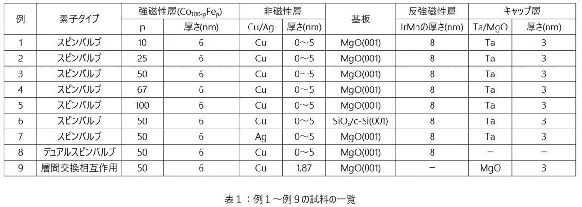
種々の組成のCo100-pFep、Cu、Ag、IrMn、Taの各ターゲットを、DC-RFマグネトロンスパッタ(エイコーエンジニアリング社製、型番ESA-0788)にセットし、表2に示すスパッタリング条件によりスパッタを行った。その後、表2に示すアニーリング条件にて、例1~例9の試料を磁場中で熱処理し、一方向磁気異方性を付与した。なお、例1~例9の試料は、フォトリソグラフィによりワイヤ状に加工した。また、予備実験において、ターゲットの組成と、強磁性層の組成とは、実質的に同一となることを組成分析から確認しているため、本願明細書では、ターゲットに用いた組成が、得られた強磁性層の組成であるものとして取り扱う。
このようにして得られた例1~例9の試料の構造を簡単のため表3にまとめて示す。
例1~例9の試料についてX線回折を行った。結果を図8に示す。例1~例9の試料について透過型電子顕微鏡(TEM、FEI社製、型番TITAN G2-200)を用いた高角度散乱暗視野走査透過型電子顕微鏡法(HAADF-STEM法)により高分解能観察を行い、電子回折パターンを得た。結果を図9~図11に示す。
例1~例9の試料に磁気特性を、4探針法を用いて測定した。詳細には、室温(25℃)にて、膜の面内方向に電流を流し、その方向と平行な方向に外部磁場を印加し、その際の抵抗値の変化を測定し、MR比を求めた。また、例3および例7の試料について、MR比、抵抗(R)および抵抗変化(dR)の温度依存性を調べた。例8の試料についてMR比のバイアス電圧依存性、ならびに、例9の試料について外部磁場に対する抵抗値の依存性を調べた。これらの結果を図12~図19に示す。
bcc-CuおよびCo100-pFep(p=0、25、50、75、100)について第一原理計算を行い、バンド構造を求めた。結果を図20および図21に示す。
以上の結果をまとめて説明する。
図8は、例1~例5および例7の試料のXRDパターンを示す図である。
図8は、例1~例5および例7の試料のXRDパターンを示す図である。
いずれの試料においても、約48°近傍にピークが現れ、これはIrMnの(002)ピークと同定され、すべての試料はエピタキシャル膜であった。例2~例5および例7の試料では、約66°にピークが現れ、これは、(002)bccの結晶構造によるピークと同定された。一方、例1の試料では、このピークが観察されなかった。このことから、例1の試料におけるCo90Fe10は、fccの結晶構造を有し、例2~例5および例7の試料におけるCo100-pFep(p=25、50、67、100)は、bccの結晶構造を有することが分かった。図示しないが、例8および例9の試料も例3と同様のXRDパターンを示すことを確認した。
図9は、例7および例3の試料のHAADF-STEM像および電子回折パターンを示す図である。
図10は、例3の試料について図9とは異なる晶帯軸から撮影したHAADF-STEM像を示す図である。
図11は、例3の試料において厚さの異なるCu層のHAADF-STEM像、逆フーリエ変換(IFFT)像および電子回折パターンを示す図である。
図10は、例3の試料について図9とは異なる晶帯軸から撮影したHAADF-STEM像を示す図である。
図11は、例3の試料において厚さの異なるCu層のHAADF-STEM像、逆フーリエ変換(IFFT)像および電子回折パターンを示す図である。
図9(a)および(b)は、それぞれ、例7および例3の試料の断面の原子分解能HAADF-STEM像を示す。像は、いずれも、Co50Fe50層の[110]晶帯軸から撮影され、Ag層およびCu層の厚さは、それぞれ、2.8nmおよび2.1nmであった。いずれの像も、エピタキシャル成長していることが示唆されるが、図9(a)のAg層とCo50Fe50層との界面に着目すると、転位(dislocation)が存在し、界面近傍では結晶に歪みが生じていることが分かる。しかしながら、図9(b)のCu層とCo50Fe50層と界面に着目すると、驚くべきことに、転位等の欠陥は、原子解像度レベルにおいて確認されず、Cu層とCo50Fe50層とがあたかも単一の材料であるかのようであった。図示しないが、例えば、Cu層の厚さが約2nmである例2、例4~例6、例8および例9の試料においても図9(b)と同様の様態であった。
図9(c)、(d)および(e)、(f)は、それぞれ、例7および例3の試料の電子回折パターンを示す。図9(c)、(d)によれば、例7の試料では、bcc-Co50Fe50(001)[110]//fcc-Ag(001)[100]の関係となっていることが分かる。一方、図9(e)、(f)によれば、例3の試料では、bcc-Co50Fe50の回折パターンと、Cuの回折パターンとは、互いに極めて類似しており、図9(c)、(d)の回折パターンの関係とは異なっていた。このことは、Cuは、bcc-Co50Fe50と同様に、bccの結晶構造を有していることを示唆する。図示しないが、例えば、Cu層の厚さが約2nmである例2、例4~例6、例8および例9の試料においても図9(e)、(f)と同様の回折パターンであった。
図10(a)および(b)は、それぞれ、図9(b)から45°時計回りおよび反時計回りに回転した際のCo50Fe50[100]および[010]晶帯軸から撮影したHAADF-STEM像を示す図である。図10(a)および(b)によれば、いずれの像も互いに類似しており、Co50Fe50層とCu層との間の界面に視認できる格子歪はない。
Cuがfccの結晶構造である場合、45°時計回りの像と、45°反時計回りの像とは、互いに異なり、Co50Fe50層とCu層との間の界面には格子歪が生じるはずである。しかしながら、上述したとおり、45°時計回りの像と、45°反時計回りの像とが、互いに類似しており、界面に格子歪が確認できないことから、Cuは、Co50Fe50の結晶構造と同様に、bccの結晶構造を有しており、Co50Fe50層およびCu層はいずれも単結晶(001)層であるといえる。
例5の試料は、B.Heinrichら,Phys.Rev.Lett.,Vol.64,No.6,1990の報告と同様に、Fe層もCu層もbccの結晶構造を有しており、単結晶(001)層であったが、Co100-pFep層およびCu層についても、同様の関係が成り立つことは本願発明者らが実験から初めて確認したことに留意されたい。
図11(a)および(b)は、それぞれ、Cu層の厚さが2.1nmおよび4.3nmである例3の試料の断面の原子分解能HAADF-STEM像を示す。図11(c)、(d)および(e)、(f)は、それぞれ、Cu層の厚さが2.1nmおよび4.3nmである例3の試料の電子回折パターンを示す。ここで、図11(a)、(c)および(d)は、図9(b)、(e)および(f)と同一である。
図11(b)によれば、Cu層の厚さが厚くなると、Cu層とCo50Fe50層と界面にわずかながら格子歪が確認されたが、図11(e)および(f)によれば、Cu層は、bccの結晶構造を維持していることが分かった。このことから、Cu層がbccの結晶構造を維持し、界面において良好な格子整合となるためには、Cu層の厚さの上限は、5nmとすることが好ましいといえる。なお、下限については、1nm以下の厚さであっても、Cu層を平坦かつ均一に成膜できる場合には、bccの結晶構造を維持するため、特に制限を設けないが、スパッタ等の汎用的な手法によって効率よく成膜することを考慮すれば、1.5nm以上とすることが好ましい。
図12は、例1~例5の試料のMR比のCu層の厚さ依存性を示す図である。
図13は、MR比のCo100-pFepのp値依存性を示す図である。
図13は、MR比のCo100-pFepのp値依存性を示す図である。
図12によれば、いずれの試料もCu層の厚さが減少するにともない、MR比が増大し、また、Cu層の厚さがさらに減少し、強磁性層が磁気的に結合すると、MR比が消失した。しかしながら、例2~例4の試料のMR比は、例1および例5の試料のそれよりも全体的に顕著に大きいことが分かる。例えば、例3の試料は、最大で25%を超えるMR比を示した。
このことから、一対のbccの結晶構造を有するCo100-pFep層と、その間に位置するbccの結晶構造を有するCu層との積層構造であって、Co100-pFep層およびCu層がいずれも単結晶(001)層である場合、このような積層構造は、高いMR比を有する磁気抵抗効果膜として機能することが示された。
また、例2~例4の試料のMR比の消失の程度は、例1および例5の試料のそれに比べて急峻であった。このことは、例2~例4の試料におけるCo100-pFep層とCu層との間の界面は、例1および例5のそれと比べて、格子歪がなく、平滑であることを示唆し、上述の図9の結果に良好に一致した。
いずれの試料においても、Cu層が1.5nm以下において強磁性層が磁気的に結合し、MR比が消失したが、これは、Cu層の膜質や平坦性を向上させることによって、高いMR比を維持できると考える。しかしながら、Co100-pFep層のp値にも依存するが、Cu層の厚さが好ましくは1.5nm以上で顕著に向上し、5nm以下までは、特別な膜質制御等(例えば、Cu層の成膜時の成膜レートや基板温度の最適化)を要することなく、高いMR比を維持することが示された。
例1の試料は、図8を参照して述べたように、fccの結晶構造を示したが、例えば、基板上にbccの結晶構造を有するCo100-pFep(20≦p≦100)などのバッファ層を設ければ、強磁性層および非磁性層のいずれもbccの結晶構造を有し、単結晶(001)層または(001)結晶面に優先配向した磁気抵抗効果素子(例えば、MgO/Co100-pFep/Co90Fe10/Cu/Co90Fe10/IrMn/Ta等)を提供できることが示唆される。
図13には、Cu層の厚さが2.5nmである例1~例5の試料のMR比の値(丸で示す)と、例1~例5の試料のMR比の最大値(四角で示す)とが示される。例2~例4の試料は、いずれも20%を超える、または、20%程度の大きなMR比を有した。一方、例1や例5の試料は、従来どおりの10%以下の小さなMR比であった。
このことから、二元系合金となるCo100-pFep層のp値は、20以上75以下、好ましくは22以上70以下、より好ましくは25以上65以下であり、なおさらに好ましくは40以上60以下であることが示された。
図14は、例3、例6および例7の試料のMR比のCu層/Ag層の厚さ依存性を示す図である。
図14において、例3の試料のMR比のCu層の厚さ依存性は、図12のそれと同一である。図14によれば、例6の試料のMR比は、例3の試料のそれよりも小さいものの、例7の試料のMR比よりも大きかった。このことから、例6の試料において、Co100-pFep層およびCu層は、(001)結晶面に優先配向しており、これにより大きなMR比が得られる磁気抵抗効果膜として機能することが示唆される。
図15は、例3および例8の試料のMR比のCu層の厚さ依存性を示す図である。
図16は、例8の試料のMR比および出力電圧のバイアス電圧依存性を示す図である。
図16は、例8の試料のMR比および出力電圧のバイアス電圧依存性を示す図である。
図15によれば、例8の試料のMR比は、例3の試料のそれよりも大きいことが分かった。このことから、単結晶(001)層または(001)面に優先配向した、強磁性層(bcc-Co100-pFep)と非磁性層(bcc-Cu)とを2以上繰り返した磁気抵抗効果膜を有する磁気抵抗効果素子は、より大きなMR比を示し、有利であることが分かった。
図16によれば、最大3.0Vまでバイアス電圧を変化させても、例8の試料のMR比は変化せず、出力電圧は線形に変化した。このことから、本発明の磁気抵抗効果素子は、磁気抵抗効果による高い電圧出力を得るのに有利であることが示された。
図17は、例3および例7の試料のMR比の温度依存性を示す図である。
図18は、例3および例7の試料の抵抗(R)および抵抗変化(dR)の温度依存性を示す図である。
図18は、例3および例7の試料の抵抗(R)および抵抗変化(dR)の温度依存性を示す図である。
図17によれば、例3の試料は、温度の低下に伴い、さらにMR比が増大し、10Kにおいて最大40%のMR比が得られた。一方、例7の試料は、温度を低下させてもMR比は10%程度の小さな値を維持し、変化しなかった。
図18では、図17で得られたMR比の温度依存性を抵抗Rと抵抗変化dRとに分けて示す。抵抗Rの温度依存性に着目すると、例3の試料および例7の試料は、いずれも、同様の温度依存性を示した。しかしながら、抵抗変化dRに着目すると、例3の試料の抵抗変化dRは、温度の低下に伴い上昇したが、例7の試料のそれは、温度の低下に伴い減少した。このことは、低温で電子の平均自由行程が長くなった際に、界面散乱のスピン非対称性の影響が大きくなり、MR比が向上したことを示し、例3の試料におけるCo100-pFep層とCu層とのマジョリティスピン電子の界面のバンド整合は、例7の試料におけるCo100-pFep層とAg層とのそれに比べて高いことを示唆する。
図19は、例9の試料のMR比の外部磁場依存性を示す図である。
図19によれば、例9の試料は、上下に同じ膜厚と同じ組成のCo50Fe50を用いているため、保磁力差が生じず、また反強磁性体による交換バイアスを加えるわけでもないが、外部磁場ゼロで明確な反平行状態が実現されており、31%もの大きなMR比を示した。このことは、例9の試料において、Co50Fe50層の磁化は、Cuを介した層間交換相互作用によって反平行状態となったことを示す。従って、これを複数積層させた人工格子を形成すれば、隣接するCo50Fe50層が交互に反平行を向いた磁化状態が実現されるため、さらに大きなMR比を示す磁気抵抗効果素子が期待できる。
図20は、bcc-Cu、bcc-Co50Fe50およびbcc-Feの第一原理計算によるバンド構造を示す図である。
図21は、(a)bcc-Co、(b)bcc-Co75Fe25および(c)bcc-Co25Fe75の第一原理計算によるバンド構造を示す図である。
図21は、(a)bcc-Co、(b)bcc-Co75Fe25および(c)bcc-Co25Fe75の第一原理計算によるバンド構造を示す図である。
図20(a)は、bcc-Cuのバンド構造であり、図20(b)および図20(c)は、それぞれ、bcc-Co50Fe50のマジョリティスピン状態およびマイノリティスピン状態のバンド構造であり、図20(d)および図20(e)は、それぞれ、bcc-Feのマジョリティスピン状態およびマイノリティスピン状態のバンド構造である。
図20(a)と図20(b)とを比較する(例えば、フェルミレベル近傍に着目する)と、bcc-Cuのバンド分散は、bcc-Co50Fe50のマジョリティスピン状態と極めて類似しており、バンド構造が良好にマッチングしている。なお、図20(a)と図20(c)とを比較すれば、bcc-Cuのバンド分散は、bcc-Co50Fe50のマイノリティスピン状態とは異なる。また、図20(a)と、図21(a)~(c)とをそれぞれ比較すると、bcc-Cuのバンド分散は、bcc-Co、bcc-Co75Fe25、bcc-Co25Fe75のマジョリティスピン状態と極めて類似しており、バンド構造が良好にマッチングしている。
この結果、アップスピン電子は、ダウンスピン電子に比べて、bcc-Co100-pFep層(ただし、0≦p≦75を満たす)とbcc-Cu層との間を容易に移動できることになる。このような高いスピンの非対称性により、大きなMR比が得られる。
一方、bcc-Co50Fe50層と同様のbcc-Feは、bcc-Cuとの格子不整合も小さいものの、図12の例5の試料に示すように、MR比は小さかった。これは、図20(a)と図20(d)および図20(e)との比較から、bcc-Cuのバンド分散は、bcc-Feのマジョリティスピン状態ともマイノリティスピン状態とも異なり、フェルミ準位(E-EF=0)におけるバンド構造の整合性がないためと考えられる。
これらから、MR比の向上には、強磁性層と非磁性層との格子整合のみならず、強磁性層と非磁性層との間のバンド構造のマッチングも重要であることが示された。本願発明者らは、体心立方(bcc)の結晶構造を有する、一般式Co100-pFepで表される層(パラメータpは、0≦p≦75を満たす)である強磁性層と、体心立方(bcc)の結晶構造を有する、Cuからなる層である非磁性層とが、図20、図21に示すように、良好なバンド構造のマッチングを示すことを見出し、さらに、これらが、単結晶(001)層であるか、または、(001)結晶面に優先配向とすることにより、界面にて格子が歪むことなく良好に格子整合し、高いMR比を達成する磁気抵抗効果素子の開発に成功した。
本発明の磁気抵抗効果素子は、CIP型で使用しても高いMR比を示すので、このような高いMR比による磁場に対する高い感度を有する磁気センサ、再生ヘッドおよび磁気記録再生装置に適用される。
100、100A、100B、300、400 磁気抵抗効果素子
110、310、410 磁気抵抗効果膜
120、120n、140 強磁性層
130、130n 非磁性層
150 基板
320 反強磁性層
500 磁気センサ
600 磁気ヘッド
610 再生ヘッド
620 記録ヘッド
611 スライダ
612、621、623 絶縁層
613 下部シールド層
614 下部ギャップ絶縁層
615 磁区制御層
616 一対の端子層
617 上部ギャップ絶縁層
618 上部シールド層
622 下部磁極
624 記録ギャップ層
625 上部磁極
626 コイル
700 磁気記録再生装置
710 ハウジング
720 アクチュエータ
730 アクチュエータアーム
740 ヘッドスライダ
750 磁気記録媒体
Claims (20)
- 磁気抵抗効果膜を備えた磁気抵抗効果素子であって、
前記磁気抵抗効果膜は、少なくとも、一対の強磁性層と、前記一対の強磁性層の間に位置する非磁性層とを備え、
前記一対の強磁性層のそれぞれは、体心立方(bcc)の結晶構造を有し、一般式Co100-pFepで表される層(パラメータpは、0≦p≦75を満たし、前記一対の強磁性層のそれぞれにおけるpは、同一または別異である)であり、
前記非磁性層は、体心立方(bcc)の結晶構造を有し、Cuからなる層であり、
前記一対の強磁性層、および、前記非磁性層のそれぞれは、単結晶(001)層であるか、または、(001)結晶面に優先配向している、磁気抵抗効果素子。 - 前記パラメータpは、0≦p≦70を満たす、請求項1に記載の磁気抵抗効果素子。
- 前記パラメータpは、p=0または22≦p≦70を満たす、請求項2に記載の磁気抵抗素子。
- 前記パラメータpは、0≦p≦65を満たす、請求項2に記載の磁気抵抗効果素子。
- 前記パラメータpは、p=0、または、25≦p≦65を満たす、請求項4に記載の磁気抵抗効果素子。
- 前記非磁性層は、1.5nm以上5nm以下の範囲の厚さを有する、請求項1~5のいずれかに記載の磁気抵抗効果素子。
- 前記一対の強磁性層のそれぞれは、1.5nm以上15nm以下の範囲の厚さを有する、請求項1~6のいずれかに記載の磁気抵抗効果素子。
- 前記磁気抵抗効果膜は、前記一対の強磁性層のうち一方と磁気的に結合する反強磁性層をさらに備える、請求項1~7のいずれかに記載の磁気抵抗効果素子。
- 前記反強磁性層は、IrMn層、FeMn層、PtMn層およびCoO層からなる群から選択される、請求項8に記載の磁気抵抗効果素子。
- 前記磁気抵抗効果膜は、前記一対の強磁性層と、前記一対の強磁性層の間に位置する前記非磁性層とからなる多層構造を2以上有し、前記2以上の多層構造のそれぞれは絶縁層によって分離している、請求項1~9のいずれかに記載の磁気抵抗効果素子。
- 前記磁気抵抗効果膜は、前記強磁性層と前記非磁性層とが繰り返し積層された人工格子構造である、請求項1~9のいずれかに記載の磁気抵抗効果素子。
- 前記強磁性層のそれぞれは、異なる保磁力を有する、請求項1~7のいずれかに記載の磁気抵抗効果素子。
- 前記磁気抵抗効果膜は基板上に位置し、
前記基板は、ガラス基板、アルミナ基板、熱酸化膜を有する/有しないSi単結晶、MgO単結晶、サファイア単結晶、SrTiO3単結晶、MgAl2O4単結晶およびTiO2単結晶からなる群から選択される、請求項1~12のいずれかに記載の磁気抵抗効果素子。 - 前記基板は、バッファ層をさらに備える、請求項13に記載の磁気抵抗効果素子。
- 前記磁気抵抗効果膜は、キャップ層をさらに備える、請求項1~14のいずれかに記載の磁気抵抗効果素子。
- 前記磁気抵抗効果素子は、前記磁気抵抗効果膜の面内方向に電流を流すCIP型、または、前記磁気抵抗効果膜の積層方向に電流を流すCPP型である、請求項1~15のいずれかに記載の磁気抵抗効果素子。
- 磁気抵抗効果素子を備えた磁気センサであって、
前記磁気抵抗効果素子は、請求項1~16のいずれかに記載の磁気抵抗効果素子である、磁気センサ。 - 磁気抵抗効果素子を備えた磁気記録再生装置用の再生ヘッドであり、
前記磁気抵抗効果素子は、請求項1~16のいずれかに記載の磁気抵抗効果素子である、再生ヘッド。 - 再生ヘッドを備えた磁気記録再生装置であって、
前記再生ヘッドは、請求項18に記載の再生ヘッドである、磁気記録再生装置。 - 記録ヘッドをさらに備える、請求項19に記載の磁気記録再生装置。
Priority Applications (2)
| Application Number | Priority Date | Filing Date | Title |
|---|---|---|---|
| US17/295,124 US11521645B2 (en) | 2018-11-29 | 2019-06-27 | Magnetoresistive element, magnetic sensor, reproducing head, and magnetic recording and reproducing device |
| JP2020558074A JP7136492B2 (ja) | 2018-11-29 | 2019-06-27 | 磁気抵抗効果素子、磁気センサ、再生ヘッドおよび磁気記録再生装置 |
Applications Claiming Priority (2)
| Application Number | Priority Date | Filing Date | Title |
|---|---|---|---|
| JP2018-223592 | 2018-11-29 | ||
| JP2018223592 | 2018-11-29 |
Publications (1)
| Publication Number | Publication Date |
|---|---|
| WO2020110360A1 true WO2020110360A1 (ja) | 2020-06-04 |
Family
ID=70852730
Family Applications (1)
| Application Number | Title | Priority Date | Filing Date |
|---|---|---|---|
| PCT/JP2019/025635 Ceased WO2020110360A1 (ja) | 2018-11-29 | 2019-06-27 | 磁気抵抗効果素子、磁気センサ、再生ヘッドおよび磁気記録再生装置 |
Country Status (3)
| Country | Link |
|---|---|
| US (1) | US11521645B2 (ja) |
| JP (1) | JP7136492B2 (ja) |
| WO (1) | WO2020110360A1 (ja) |
Citations (4)
| Publication number | Priority date | Publication date | Assignee | Title |
|---|---|---|---|---|
| JPH06325934A (ja) * | 1992-10-30 | 1994-11-25 | Toshiba Corp | 磁気抵抗効果素子 |
| US20110007420A1 (en) * | 2009-07-10 | 2011-01-13 | Tdk Corporation | Magnetoresistive effect element in cpp-type structure and magnetic disk device |
| JP2015049927A (ja) * | 2013-08-30 | 2015-03-16 | シーゲイト テクノロジー エルエルシー | 二重リーダー構造 |
| JP2015212996A (ja) * | 2015-06-30 | 2015-11-26 | 株式会社東芝 | 磁気抵抗効果素子、磁気抵抗効果素子の製造方法、磁気ヘッド、磁気記録再生装置、磁気メモリ |
Family Cites Families (13)
| Publication number | Priority date | Publication date | Assignee | Title |
|---|---|---|---|---|
| US5549978A (en) | 1992-10-30 | 1996-08-27 | Kabushiki Kaisha Toshiba | Magnetoresistance effect element |
| US6111784A (en) * | 1997-09-18 | 2000-08-29 | Canon Kabushiki Kaisha | Magnetic thin film memory element utilizing GMR effect, and recording/reproduction method using such memory element |
| JP4382333B2 (ja) * | 2002-03-28 | 2009-12-09 | 株式会社東芝 | 磁気抵抗効果素子、磁気ヘッド及び磁気再生装置 |
| JP2005347418A (ja) * | 2004-06-01 | 2005-12-15 | Alps Electric Co Ltd | 磁気検出素子 |
| US20080016653A1 (en) * | 2006-07-19 | 2008-01-24 | Amelia Baradzi | Ergonomic handle for push tools |
| JP4550777B2 (ja) * | 2006-07-07 | 2010-09-22 | 株式会社東芝 | 磁気抵抗効果素子の製造方法、磁気抵抗効果素子、磁気ヘッド、磁気記録再生装置及び磁気メモリ |
| JP2008252008A (ja) * | 2007-03-30 | 2008-10-16 | Toshiba Corp | 磁気抵抗効果素子、およびその製造方法 |
| US8780507B2 (en) * | 2007-12-28 | 2014-07-15 | HGST Netherlands B.V. | Read transducer and magnetic storage system implementing same |
| WO2011064822A1 (ja) * | 2009-11-27 | 2011-06-03 | 株式会社 東芝 | 磁気抵抗効果素子、及び磁気記録再生装置 |
| US9082888B2 (en) * | 2012-10-17 | 2015-07-14 | New York University | Inverted orthogonal spin transfer layer stack |
| JP6444276B2 (ja) * | 2015-07-28 | 2018-12-26 | 国立研究開発法人物質・材料研究機構 | 磁気抵抗素子、その用途及び製造方法、並びにホイスラー合金の製造方法 |
| KR20170074255A (ko) * | 2015-12-21 | 2017-06-30 | 에스케이하이닉스 주식회사 | 전자 장치 |
| US10097435B2 (en) * | 2016-11-02 | 2018-10-09 | Johnson Controls Technology Company | Systems and methods for real-time detection and communication of health and performance degradation in a distributed building automation network |
-
2019
- 2019-06-27 JP JP2020558074A patent/JP7136492B2/ja active Active
- 2019-06-27 US US17/295,124 patent/US11521645B2/en active Active
- 2019-06-27 WO PCT/JP2019/025635 patent/WO2020110360A1/ja not_active Ceased
Patent Citations (4)
| Publication number | Priority date | Publication date | Assignee | Title |
|---|---|---|---|---|
| JPH06325934A (ja) * | 1992-10-30 | 1994-11-25 | Toshiba Corp | 磁気抵抗効果素子 |
| US20110007420A1 (en) * | 2009-07-10 | 2011-01-13 | Tdk Corporation | Magnetoresistive effect element in cpp-type structure and magnetic disk device |
| JP2015049927A (ja) * | 2013-08-30 | 2015-03-16 | シーゲイト テクノロジー エルエルシー | 二重リーダー構造 |
| JP2015212996A (ja) * | 2015-06-30 | 2015-11-26 | 株式会社東芝 | 磁気抵抗効果素子、磁気抵抗効果素子の製造方法、磁気ヘッド、磁気記録再生装置、磁気メモリ |
Also Published As
| Publication number | Publication date |
|---|---|
| JPWO2020110360A1 (ja) | 2021-10-21 |
| US20220005499A1 (en) | 2022-01-06 |
| US11521645B2 (en) | 2022-12-06 |
| JP7136492B2 (ja) | 2022-09-13 |
Similar Documents
| Publication | Publication Date | Title |
|---|---|---|
| JP5988019B2 (ja) | 強磁性トンネル接合体とそれを用いた磁気抵抗効果素子及びスピントロニクスデバイス | |
| US20080068767A1 (en) | Exchange-coupled film, method for making exchange-coupled film, and magnetic sensing element including exchange-coupled film | |
| US7446987B2 (en) | Composite hard bias design with a soft magnetic underlayer for sensor applications | |
| US11871681B2 (en) | Magnetoresistance effect element | |
| JP5763892B2 (ja) | ハードバイアス構造の形成方法 | |
| JP3756758B2 (ja) | 交換結合膜と、この交換結合膜を用いた磁気抵抗効果素子、ならびに前記磁気抵抗効果素子を用いた薄膜磁気ヘッド | |
| JP3839644B2 (ja) | 交換結合膜と、この交換結合膜を用いた磁気抵抗効果素子、ならびに前記磁気抵抗効果素子を用いた薄膜磁気ヘッド | |
| US7760473B2 (en) | Magnetoresistance element employing Heusler alloy as magnetic layer | |
| JP2637360B2 (ja) | 磁気抵抗効果素子 | |
| CN107408625A (zh) | 磁阻效应元件 | |
| US7515388B2 (en) | Composite hard bias design with a soft magnetic underlayer for sensor applications | |
| US9183857B2 (en) | Magnetic devices having shields including a nickel alloy | |
| JPH10188235A (ja) | 磁気抵抗効果膜及びその製造方法 | |
| JP2000022239A (ja) | 磁気抵抗効果膜および磁気抵抗効果型ヘッド | |
| JP2002171010A (ja) | 交換結合膜と、この交換結合膜を用いた磁気抵抗効果素子、ならびに前記磁気抵抗効果素子を用いた薄膜磁気ヘッド | |
| US7876536B2 (en) | Multilayered film having crystal grains grown at an inclination to a substrate, and magnetoresistive head using the film | |
| US20060215330A1 (en) | Magnetic sensing element containing quaternary Heusler alloy Co2Mn (Ge1-xSnx) which constitutes a free magnetic layer or pinned magnetic layer | |
| JP2018098305A (ja) | 高感度面直通電巨大磁気抵抗素子用積層膜、高感度面直通電巨大磁気抵抗素子、及びその用途 | |
| US11521645B2 (en) | Magnetoresistive element, magnetic sensor, reproducing head, and magnetic recording and reproducing device | |
| Huai et al. | IrMn based spin-filter spin-valves | |
| JP3488545B2 (ja) | 磁気抵抗効果素子、磁気抵抗効果ヘッドおよび磁気再生装置 | |
| JPH0887722A (ja) | 磁気抵抗効果素子および磁気変換素子 | |
| KR0136073B1 (ko) | 자기 저항 효과 소자 | |
| JPH10321435A (ja) | 磁気抵抗効果素子及びその製造方法 | |
| JP2025011895A (ja) | トンネル磁気抵抗センサおよびその製造方法 |
Legal Events
| Date | Code | Title | Description |
|---|---|---|---|
| 121 | Ep: the epo has been informed by wipo that ep was designated in this application |
Ref document number: 19889665 Country of ref document: EP Kind code of ref document: A1 |
|
| ENP | Entry into the national phase |
Ref document number: 2020558074 Country of ref document: JP Kind code of ref document: A |
|
| NENP | Non-entry into the national phase |
Ref country code: DE |
|
| 122 | Ep: pct application non-entry in european phase |
Ref document number: 19889665 Country of ref document: EP Kind code of ref document: A1 |