WO2020105627A1 - 高出力テラヘルツ発振器 - Google Patents
高出力テラヘルツ発振器Info
- Publication number
- WO2020105627A1 WO2020105627A1 PCT/JP2019/045251 JP2019045251W WO2020105627A1 WO 2020105627 A1 WO2020105627 A1 WO 2020105627A1 JP 2019045251 W JP2019045251 W JP 2019045251W WO 2020105627 A1 WO2020105627 A1 WO 2020105627A1
- Authority
- WO
- WIPO (PCT)
- Prior art keywords
- cavity resonator
- conductor piece
- bow
- rtd
- conductor
- Prior art date
- Legal status (The legal status is an assumption and is not a legal conclusion. Google has not performed a legal analysis and makes no representation as to the accuracy of the status listed.)
- Ceased
Links
Images




Classifications
-
- H—ELECTRICITY
- H03—ELECTRONIC CIRCUITRY
- H03B—GENERATION OF OSCILLATIONS, DIRECTLY OR BY FREQUENCY-CHANGING, BY CIRCUITS EMPLOYING ACTIVE ELEMENTS WHICH OPERATE IN A NON-SWITCHING MANNER; GENERATION OF NOISE BY SUCH CIRCUITS
- H03B5/00—Generation of oscillations using amplifier with regenerative feedback from output to input
- H03B5/18—Generation of oscillations using amplifier with regenerative feedback from output to input with frequency-determining element comprising distributed inductance and capacitance
- H03B5/1817—Generation of oscillations using amplifier with regenerative feedback from output to input with frequency-determining element comprising distributed inductance and capacitance the frequency-determining element being a cavity resonator
-
- H—ELECTRICITY
- H01—ELECTRIC ELEMENTS
- H01Q—ANTENNAS, i.e. RADIO AERIALS
- H01Q23/00—Antennas with active circuits or circuit elements integrated within them or attached to them
-
- H—ELECTRICITY
- H01—ELECTRIC ELEMENTS
- H01Q—ANTENNAS, i.e. RADIO AERIALS
- H01Q1/00—Details of, or arrangements associated with, antennas
- H01Q1/36—Structural form of radiating elements, e.g. cone, spiral, umbrella; Particular materials used therewith
- H01Q1/38—Structural form of radiating elements, e.g. cone, spiral, umbrella; Particular materials used therewith formed by a conductive layer on an insulating support
-
- H—ELECTRICITY
- H01—ELECTRIC ELEMENTS
- H01Q—ANTENNAS, i.e. RADIO AERIALS
- H01Q9/00—Electrically-short antennas having dimensions not more than twice the operating wavelength and consisting of conductive active radiating elements
- H01Q9/04—Resonant antennas
- H01Q9/16—Resonant antennas with feed intermediate between the extremities of the antenna, e.g. centre-fed dipole
- H01Q9/28—Conical, cylindrical, cage, strip, gauze, or like elements having an extended radiating surface; Elements comprising two conical surfaces having collinear axes and adjacent apices and fed by two-conductor transmission lines
-
- H—ELECTRICITY
- H03—ELECTRONIC CIRCUITRY
- H03B—GENERATION OF OSCILLATIONS, DIRECTLY OR BY FREQUENCY-CHANGING, BY CIRCUITS EMPLOYING ACTIVE ELEMENTS WHICH OPERATE IN A NON-SWITCHING MANNER; GENERATION OF NOISE BY SUCH CIRCUITS
- H03B7/00—Generation of oscillations using active element having a negative resistance between two of its electrodes
- H03B7/02—Generation of oscillations using active element having a negative resistance between two of its electrodes with frequency-determining element comprising lumped inductance and capacitance
- H03B7/06—Generation of oscillations using active element having a negative resistance between two of its electrodes with frequency-determining element comprising lumped inductance and capacitance active element being semiconductor device
- H03B7/08—Generation of oscillations using active element having a negative resistance between two of its electrodes with frequency-determining element comprising lumped inductance and capacitance active element being semiconductor device being a tunnel diode
-
- H—ELECTRICITY
- H03—ELECTRONIC CIRCUITRY
- H03B—GENERATION OF OSCILLATIONS, DIRECTLY OR BY FREQUENCY-CHANGING, BY CIRCUITS EMPLOYING ACTIVE ELEMENTS WHICH OPERATE IN A NON-SWITCHING MANNER; GENERATION OF NOISE BY SUCH CIRCUITS
- H03B7/00—Generation of oscillations using active element having a negative resistance between two of its electrodes
- H03B7/12—Generation of oscillations using active element having a negative resistance between two of its electrodes with frequency-determining element comprising distributed inductance and capacitance
- H03B7/14—Generation of oscillations using active element having a negative resistance between two of its electrodes with frequency-determining element comprising distributed inductance and capacitance active element being semiconductor device
-
- H—ELECTRICITY
- H10—SEMICONDUCTOR DEVICES; ELECTRIC SOLID-STATE DEVICES NOT OTHERWISE PROVIDED FOR
- H10D—INORGANIC ELECTRIC SEMICONDUCTOR DEVICES
- H10D8/00—Diodes
- H10D8/70—Tunnel-effect diodes
-
- H—ELECTRICITY
- H03—ELECTRONIC CIRCUITRY
- H03B—GENERATION OF OSCILLATIONS, DIRECTLY OR BY FREQUENCY-CHANGING, BY CIRCUITS EMPLOYING ACTIVE ELEMENTS WHICH OPERATE IN A NON-SWITCHING MANNER; GENERATION OF NOISE BY SUCH CIRCUITS
- H03B2200/00—Indexing scheme relating to details of oscillators covered by H03B
- H03B2200/006—Functional aspects of oscillators
- H03B2200/0084—Functional aspects of oscillators dedicated to Terahertz frequencies
Definitions
- the present invention oscillates a frequency in a terahertz (THz) frequency band (about 0.1 THz to 10 THz) located between an electric wave and a light wave, and is capable of stably outputting a high oscillation frequency at room temperature.
- a terahertz oscillator capable of high output in which a resonant tunneling diode (RTD (Resonant Tunneling Diode)) element having a semiconductor nanostructure is integrated with a cavity resonator having two cavities and a bowtie antenna composed of two conductor pieces. It is about.
- RTD Resonant Tunneling Diode
- the terahertz (THz) frequency band (about 0.1 THz to 10 THz) located between radio waves and light waves is an undeveloped frequency band, but if put to practical use, it is expected to have various applications such as imaging and high-speed communication. ..
- THz terahertz
- development of a small terahertz oscillator is indispensable.
- a terahertz oscillator using a resonant tunnel diode (RTD) element having a semiconductor nanostructure has been studied.
- This terahertz oscillator is currently the only electronic device that can oscillate a frequency of 1 to 2 THz at room temperature even if it is used alone.
- this terahertz oscillator has a problem that its output is very small, about 10 ⁇ W, and therefore its application is limited to a narrow range.
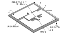
- FIG. 1 shows a conventional terahertz oscillator, in which a lower electrode 4 is layered on an InP substrate 3 having a side of about 1 mm, and a slot having a long (10 to 20 ⁇ m) concave portion is formed substantially in the center of the lower electrode 4.
- the antenna 2 is provided.
- an upper electrode 5 and a stabilizing resistor 6 are provided on the InP substrate 3, and a negative V (as shown in FIG. 3) via a MIM (Metal Insulator Metal) capacitor 7 at the tip of the upper electrode 5.
- a resonant tunneling diode (RTD) 1 having a voltage-I (current) characteristic is provided.
- the stabilizing resistor 6 is connected between the lower electrode 4 and the upper electrode 5 for stabilizing the oscillation operation, and the stabilizing resistor 6 is composed of, for example, an InGaAs sheet.
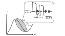
- the resonant tunnel diode 1 when a bias voltage is applied with a DC bias, electrons tunnel through the quantum level in the well, a tunnel current flows, and when a bias voltage is further applied, the quantum level in the well is increased. When becomes below the bottom of the conduction band of the emitter, electrons cannot tunnel and the current decreases, resulting in the VI characteristic as shown in FIG.
- An electromagnetic wave can be oscillated and amplified by using the differential negative resistance characteristic "-G RTD " in which the current decreases.
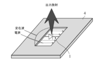
- the resonant tunnel diode 1 has a parasitic capacitance C RTD in parallel with the differential negative resistance “ ⁇ G RTD ”, and is radiated in a direction perpendicular to the standing wave of the electric field, as shown in FIG.
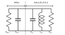
- the output is determined by the radiation resistance of the slot antenna 2. Since the slot antenna 2 is represented by the LC resonance circuit and the radiation loss G ant , the equivalent circuit of this oscillator is the equivalent circuit shown in FIG.
- the oscillation start condition is when the positive value G RTD of the differential negative resistance characteristic is equal to or higher than the radiation loss G ant as shown in the following formula 1, and the oscillation is performed at the frequency f OSC shown in the following formula 2.
- the slot antenna 2 Since the slot antenna 2 has a large inductance, it is necessary to reduce the capacitance of the RTD1 in order to increase the oscillation frequency f OSC up to the terahertz band. For that purpose, it is necessary to reduce the mesa area (the area of the upper surface) of the RTD1. was there. Therefore, there is a trade-off problem that the current flowing through the RTD 1 decreases and the output decreases as the frequency increases. If the slot antenna 2 is made as short as possible and the inductance is made small, the oscillation frequency becomes high. However, in this case, the radiation resistance of the slot antenna 2 becomes large, which also causes a decrease in output, which is a trade-off problem. Occurs.
- Patent Document 2 a terahertz oscillator using an intrinsic Josephson junction between a superconducting layer and an insulating layer has been proposed, and an oscillator using this superconducting element. Allows the frequency to be changed.
- the terahertz oscillator of Patent Document 2 has a problem that the operation is limited only at an extremely low temperature, and the superconducting layer must be held and managed at an extremely low temperature. Therefore, a terahertz oscillator capable of high output even at room temperature appears. Is desired.
- Patent Document 3 proposes a terahertz oscillator having a structure in which varactor diodes are arranged in parallel in an RTD and a DC voltage is separately applied to oscillate.
- the terahertz frequency can be continuously varied at room temperature, but the output is small at about 0.3 to 10 ⁇ W, and the appearance of a terahertz oscillator capable of high output is desired.
- the present invention has been made under the circumstances as described above, and an object of the present invention is to provide a high-output terahertz oscillator that is small in size and can stably oscillate in the terahertz frequency band even at room temperature. ..
- the present invention relates to a high power terahertz oscillator, and the above object of the present invention is to dispose a bowtie antenna composed of a first conductor piece and a second conductor piece on a substrate, and to have two cavities in a resonance part of the bowtie antenna.
- the above object of the present invention is that the bottom surface of the resonant tunnel diode is in contact with the top surface of the second conductor piece, or the first conductor piece of the bow-tie antenna and the cavity resonator are integrated.
- the first conductor piece and the second conductor piece, the cavity resonator are good conductors
- the substrate is semi-insulating, or
- An insulator thin film is provided between the first conductor piece and the second conductor piece of the bow-tie antenna, between the bottom of the cavity resonator and the second conductor piece, or
- a recess is formed in the second conductor piece of the bow tie antenna, a conductor bridge extending from the cavity resonator is connected to the upper surface of the substrate in the recess, and the conductor bridge and the second conductor piece are connected to each other. This is achieved more effectively by connecting the stabilizing resistor to the side surface.
- the output was about 10 ⁇ W at an oscillation frequency of about 1 THz, but according to the high-output terahertz oscillator of the present invention, about 7 mW at an oscillation frequency of about 1 THz, about 700 times Improved output was obtained. Moreover, it stably oscillates at room temperature.
- FIG. 10 is an equivalent circuit diagram of a terahertz oscillator using a conventional RTD. It is a perspective view which shows the structural example of the high output terahertz oscillator which concerns on this invention.
- FIG. 3 is a partial detailed view of a high power terahertz oscillator according to the present invention.
- FIG. 7 is a sectional view showing an example of a sectional structure of a terahertz oscillator according to the present invention (YY ′ in FIG. 6).
- FIG. 7 is a sectional view showing an example of a sectional structure of a terahertz oscillator according to the present invention (ZZ ′ in FIG. 6).
- FIG. 9 is a cross-sectional view showing a cross-sectional structure example (X-X ′ in FIG. 6) and another modification example of the terahertz oscillator according to the present invention.
- It is a schematic diagram which shows the cross-section example of RTD. It is an equivalent circuit diagram of a terahertz oscillator according to the present invention.
- FIG. 6 is a cross-sectional view showing another structural example of the cavity oscillator. It is a perspective view which shows the structural example of the high output terahertz oscillator which concerns on this invention. It is a characteristic view which shows the characteristic example of the oscillator of FIG.
- the present invention investigates the cause of the small output of a conventional slot antenna integrated RTD oscillator in a terahertz oscillator using a resonant tunnel diode element (hereinafter, simply referred to as “RTD”) having a semiconductor nanostructure, and causes the small output.
- RTD resonant tunnel diode element
- a small size about 1 mm square, height about several ⁇ m
- a cavity resonator having two elongated cavities and a bow tie antenna (bow tie angle ⁇ ) consisting of two conductor pieces are integrated in an RTD.
- a cavity resonator having two long cavities having a rectangular cross section or a trapezoidal cross section is arranged in the resonance portion of the bow-tie antenna that determines the oscillation frequency.
- the two cavities of the cavity resonator are partitioned by a wall member that hangs from the ceiling.
- the oscillator output is radiated by a bowtie antenna that is spatially separated from the cavity resonator.
- a rectangular cross section is provided between the bottom surface of the wall member of the cavity resonator and the conductor piece of the bowtie antenna.
- a long RTD is arranged, and the RTD is biased by an upper electrode connected to the cavity resonator and a lower electrode connected to the conductor piece of the bow-tie antenna. That is, the upper electrode of the RTD serves as the bottom surface of the wall member, and the upper surface of the bowtie antenna serves as the lower electrode of the RTD. Further, one of the bow tie antennas (one conductor piece) and a part (the side surface or the top surface) of the cavity resonator connected to the other conductor piece facing the bow tie antenna are feeding portions.
- the cavity resonator is made of good conductors such as gold (Au), copper (Cu), silver (Ag), platinum (Pt) including the ceiling and wall members, and the bow tie antenna (two conductor pieces) is also made of gold. It is made of a good conductor such as (Au), copper (Cu), silver (Ag), platinum (Pt).
- the cavity resonator can widen the surface through which the high-frequency current flows, the inductance can be significantly reduced compared to the slot antenna, and the oscillation frequency can be increased without reducing the RTD capacitance. Further, since the differential negative resistance can be increased by increasing the RTD mesa area, it is possible to increase the output.
- FIG. 5 is an external perspective view of a high-power terahertz oscillator 10 according to the present invention, which is formed on the upper surface of a semi-insulating (SI) substrate 11 (about 1 mm square and about several ⁇ m in height) made of InP.
- a bow tie antenna 20 is provided which is made of a good conductor such as gold (Au) and has conductor bows 21 and 22 having a bow tie angle ⁇ .
- the conductor pieces 21 and 22 of the bow-tie antenna 20 are line-symmetrical and are rectangular in shape as a whole, and the opposing resonance parts are inclined toward both sides, respectively. The angles form a bow tie angle ⁇ .
- the conductor pieces 21 and 22 are made of a good conductor such as gold (Au).
- An RTD 40 and a cavity resonator 30 are arranged in a resonance part where the two conductor pieces 21 and 22 of the bow tie antenna 20 face each other.
- a detailed perspective view of the RTD 40 and the cavity resonator 30 is shown in FIG.
- the -Y 'section is shown in FIG. 7, the ZZ' section is shown in FIG. 8, and the XX 'section is shown in FIG. 9 (A).
- the cavity resonator 30 is also made of a good conductor such as gold (Au). 7 and 8, the conductor piece 21 of the bow tie antenna 20 and the cavity resonator 30 are separate bodies so that the conductor piece 21 of the bow tie antenna 20 and the cavity resonator 30 can be easily identified. However, it is actually an integral structure of a good conductor such as gold (Au). Since they are all good conductors, they may be in contact with each other as separate bodies.
- two conductor pieces 21 and 22 forming the bow tie antenna 20 are arranged at a bow tie angle ⁇ on the upper surface of a semi-insulating (SI) substrate 11 made of InP.
- SI semi-insulating
- a cavity resonator 30 having two long cavities 31 and 32 having a rectangular cross section is arranged.
- a part of the conductor piece 22 of the bow-tie antenna 20 serves as a power feeding portion 22A for applying a bias (DC voltage), and a part (side surface or upper surface) of the cavity resonator 30 facing this is applied for bias (DC voltage).
- Power supply unit 33 is provided to supply unit 33.
- the two cavities 31 and 32 of the cavity resonator 30 are partitioned by a plate-shaped wall member 34 that hangs down from the central portion of the ceiling, and the front and back surfaces of the cavities 31 and 32 are separated.
- both are open (open) as shown in FIG.
- An elongated RTD 40 having a rectangular cross section is arranged between the bottom of the wall member 34 of the cavity resonator 30 and the upper surface of the conductor piece 22 of the bow tie antenna 20, and the RTD 40 is shown in FIG.
- the cavities 31 and 32 extend from the front surface (open) to the back surface (open).
- the bottom surface of the cavity resonator 30 and the conductor piece 22 of the bow tie antenna 20 are separated by the insulator thin film 12 having the same thickness as the RTD 40 (about 2 ⁇ m).
- the insulator thin film 12 extends to the outside of the cavity 31 and bends downward to electrically insulate the conductor pieces 21 and 22.
- the insulating thin film 12 having an L-shaped cross section is an insulating material such as SiO 2 .
- a rectangular recess 22B is provided in a portion of the conductor piece 22 of the bow-tie antenna 20 near the cavity resonator 30, and the cavity resonator 30 is provided in the recess 22B.
- An L-shaped conductor bridge 35 extending from the side surface is provided.
- the stabilizing resistor 50 suppresses parasitic oscillation of several gigahertz and causes stable terahertz oscillation, and the conductor bridge 35 has a function of inductance (Ls).
- Ls inductance
- the opening surface of the cavity resonator 30 and the stabilizing resistor 50 are not coupled to each other to cause a loss, and the output is not limited by this.
- the shape of the recess 22B is not limited to a rectangle, but may be an ellipse or a circle.
- One of the feeding parts (22A) to which the bias is applied is applied to the conductor piece 22 of the bow-tie antenna 20, becomes the lower electrode 40ED of the RTD 40 through the conductor piece 22, and the other feeding part (33) is a side surface of the cavity resonator 30.
- it is applied to the upper surface and becomes the upper electrode 40EU of the RTD 40 through the wall member 34 of the cavity resonator 30.
- the output from the oscillator circuit passes through the insulator thin film 12 between the side surface and the bottom surface and is radiated from between the electrodes (conductor pieces 21 and 22) of the bow tie antenna 20. Since the insulator thin film 12 is sufficiently thin (about 2 ⁇ m), the coupling between the cavity resonator 30 and the bow tie antenna 20 is small, so that the radiation resistance Ra of the bow tie antenna 20 is hardly affected by the cavity resonator 30.
- the cavity resonator 30 and the RTD 40 form an oscillation circuit.
- the oscillation frequency is determined by the inductance of the cavity resonator 30 and the capacitance of the RTD 40.
- the inductance of the cavity resonator 30 is small, it is possible to use an RTD with a large mesa area, and by using the RTD 40 with a large mesa area, it is possible to increase the oscillation frequency. Output can be realized.
- n is provided between two upper electrodes 40EU and a lower electrode 40ED each having a three-layer structure (Au / Pd / Ti) of gold (Au), palladium (Pd), and titanium (Ti).
- + -GaInAs (50nm), n-GaInAs (50nm), u-GaInAs (5nm), AlAs (1.5nm), GaInAs (4.5nm), AlAs (1.5nm), u-GaInAs (5nm), n-GaInAs ( 50 nm) and n + -GaInAs (400 nm) are arranged. As shown in FIGS.
- the upper electrode 40EU corresponds to the bottom of the wall member 34 of the cavity resonator 30, and the lower electrode 40ED corresponds to the upper surface of the conductor piece 22 of the bow-tie antenna 20.
- the bottom layer of FIG. 10 is a semi-insulating substrate 11 (SI-InP).
- FIG. 11 shows an equivalent circuit of the terahertz oscillator 10 of the present invention.
- the radiation resistance Ra of the bow-tie antenna 20 and the inductance Lr of the cavity resonator 30 are independent of each other, and the oscillation frequency of the terahertz oscillator and the output trade-off relationship are shown. It can be resolved.
- the cavity resonator 30 can significantly reduce the inductance Lr as compared with the slot antenna, and can increase the oscillation frequency without reducing the capacitance of the RTD 40, and thus the large-area RTD having a large mesa area.
- the element enables high output.
- the radiation resistance Ra of the bow tie antenna 20 becomes independent of the inductance Lr of the cavity resonator.
- the terahertz oscillator 10 of the present invention is simulated when the mesa area of the RTD 40 is changed.
- the characteristics are shown in FIG. 12, and in this example, the width W and the depth L of the cavity resonator 30 are 32 ⁇ m, and the height H is 2 ⁇ m.
- the frequency band is 1.0 to 2.0 THz, and the maximum output power is about 8 mW.
- the bow tie antenna 20 can change the radiation impedance according to the bow tie angle ⁇ , and the output can be maximized by matching with the RTD 40.
- both ends of the cavities 31 and 32 of the cavity resonator 30 are open (short circuit), but in the example of FIG. 9B, one of the cavity resonators 30 is closed (short circuit) structure. Is.
- a standing wave having an electric field of 0 on the closed side (short-circuit side) is distributed inside the cavity resonator 30, and at a frequency higher than that of the cavity resonator with both ends open (FIG. 9A). It resonates and the oscillation frequency increases.
- both ends of the cavity resonator 30 may be closed (short-circuited), which is not open.
- a standing wave in which the electric field is 0 is distributed at both ends inside the cavity resonator 30 and resonates at a higher frequency than when only one side is blocked (FIG. 9B). The oscillation frequency becomes higher.
- cavities 31 and 32 of the cavity resonator 30 have a rectangular cross-sectional shape in the above description, they may have a trapezoidal shape as shown in FIG.
- the cavities 31 and 32 of the cavity resonator 30 are arranged in parallel to the bow tie angle ⁇ of the bow tie antenna 20, that is, parallel to the conductor pieces 21 and 22, but as shown in FIG.
- the cavities 31 and 32 of 30 may be arranged at right angles to the resonance parts of the conductor pieces 21 and 22.
- a long RTD 40 is arranged in the center of the cavity resonator 30 perpendicularly to the opening surface from one opening surface to the other opening surface.
- the upper part and the lower part of the RTD 40 are connected to the inside of the top surface and the inside of the bottom surface of the cavity resonator 30, respectively, and the bottom surface of the cavity resonator 30 and other parts are separated by an insulator thin film inserted between the bottom surface and the side surface.
- the admittance of the cavity resonator 30 and the bowtie antenna 20 was obtained by an electromagnetic field simulator (HFSS, Ansys), and the oscillation characteristics were analyzed together with the characteristics of the RTD 40. As a result, the characteristics shown in FIG. 15 were obtained. .. In FIG. 15, the output power [mW] is obtained using the bow tie angle [deg] and the RTD mesa area as parameters, and the output power of 2 mW or more can be expected at the oscillation frequency of 1.5 THz by optimizing the bow tie angle.
- HFSS electromagnetic field simulator
- the high-power terahertz oscillator of the present invention By using the high-power terahertz oscillator of the present invention, it becomes possible to realize a compact chip for measuring the absorption spectrum of a substance existing in the terahertz frequency band, the fields of imaging and analysis in chemistry and medicine, and large-capacity radio waves using terahertz waves. It is thought that it can promote the further development of the field of communication.
- Resonant tunnel diode 2 slot antenna 3 substrate 4 lower electrode 5 upper electrode 6 stabilizing resistor 10 high power terahertz oscillator 11 substrate (InP) 12 Insulator Thin Film 20 Bowtie Antenna 21, 22 Conductor Piece 30 Cavity Resonator 31, 32 Cavity 34 Wall Member 35 Conductor Bridge 40 Resonant Tunnel Diode (RTD) 50 Stabilizing resistance
Landscapes
- Waveguide Aerials (AREA)
- Inductance-Capacitance Distribution Constants And Capacitance-Resistance Oscillators (AREA)
Abstract
【課題】小型であり、室温においてもテラヘルツ周波数帯での発振が安定的に可能な高出力のテラヘルツ発振器を提供する。 【解決手段】基板上にボウタイアンテナが配置され、ボウタイアンテナの給電部に2つの空洞を有する空洞共振器が配設され、空洞を区画する底部に沿って長形状の共鳴トンネルダイオード(RTD)が配設された構造で、共鳴トンネルダイオード、ボウタイアンテナ及び空洞共振器により、室温において、テラヘルツ周波数帯で安定的に発振する。
Description
本発明は、電波と光波の中間に位置するテラヘルツ(THz)周波数帯(約0.1THz~10THz)の周波数を発振すると共に、発振周波数を室温で安定的に高出力することが可能なテラヘルツ発振器に関し、特に半導体ナノ構造による共鳴トンネルダイオード(RTD(Resonant Tunneling Diode))素子に、2つの空洞を有する空洞共振器と、2枚の導体片で成るボウタイアンテナとを集積した高出力可能なテラヘルツ発振器に関するものである。
電波と光波の中間に位置するテラヘルツ(THz)周波数帯(約0.1THz~10THz)は未開発の周波数帯であるが、実用化されればイメージングや高速通信など様々な応用が期待されている。そのためには、小型のテラヘルツ発振器の開発が必要不可欠となる。その1つとして、半導体ナノ構造による共鳴トンネルダイオード(RTD)素子を用いたテラヘルツ発振器が研究されてきた。このテラヘルツ発振器は、現在、単体でも室温で1~2THzの周波数を発振できる唯一の電子デバイスである。しかしながら、このテラヘルツ発振器は出力が10μW程度と非常に小さいことが問題となっており、そのため応用が狭い範囲に制限されている。
図1は従来のテラヘルツ発振器を示しており、約1mm四方のInP基板3の上部に下部電極4が層設され、下部電極4のほぼ中央部に長形状(10~20μm)の凹部で成るスロットアンテナ2が配設されている。また、InP基板3上には上部電極5及び安定化抵抗6が配設され、上部電極5の先端部にMIM(Metal Insulator Metal)キャパシタ7を経て、図3に示すような負性のV(電圧)-I(電流)特性を有する共鳴トンネルダイード(RTD)1が配設されている。安定化抵抗6は下部電極4及び上部電極5の間に発振動作安定化のために接続され、安定化抵抗6は例えばInGaAsシートで構成されている。共鳴トンネルダイード1はDCバイアスでバイアス電圧を印加すると、井戸内の量子準位を介して電子がトンネルし、トンネル電流が流れ、さらにバイアス電圧を印加していくと、井戸内の量子準位がエミッタの伝導帯の底よりも下になったところで、電子がトンネルすることが出来なくなって電流が減少するため、図3に示すようなV-I特性となる。電流の減少する微分負性抵抗特性“-GRTD”を用いることによって、電磁波を発振・増幅させることが出来る。また、共鳴トンネルダイオード1は微分負性抵抗“-GRTD”と並列に寄生容量CRTDを持っており、図2に示すように、電界の定在波に対して垂直方向に放射される。出力はスロットアンテナ2の放射抵抗により決まる。スロットアンテナ2はLCの共振回路と放射損失Gantで表されるため、この発振器の等価回路は図4に示す等価回路となる。発振開始条件は、下記数1に示すように微分負性抵抗特性の正値GRTDが放射損失Gant以上になったときであり、また、下記数2で示される周波数fOSCで発振する。


スロットアンテナ2のインダクタンスが大きいために、発振周波数fOSCをテラヘルツ帯まで高くするには、RTD1のキャパシタンスを小さくする必要があり、そのためにはRTD1のメサ面積(上表面の面積)を小さくする必要があった。このため、RTD1を流れる電流が減少し、周波数が高いほど出力が減少してしまうというトレードオフの問題がある。スロットアンテナ2をできるだけ短くして、インダクタンスを小さくすれば発振周波数は高くなるが、この場合はスロットアンテナ2の放射抵抗が大きくなり、これによって、やはり出力が低下してしまうというトレードオフの問題が生じる。
M. Asada, S. Suzuki, and N. Kishimoto,"Resonant tunneling diodes for sub-terahertz and terahertz oscillators", Japanese Journal of Applied Physics, vol. 47, no. 6, pp. 4375-4384, 2008.
M. Asada and S. Suzuki, "Room-temperature oscillation of resonant tunneling diodes close to 2THz and their functions for various applications", Journal of Infrared, Millimeter, and Terahertz Waves, vol. 37, pp. 1185-1198, 2016.
また、特開2006-210585号公報(特許文献2)に示されるように、超電導層と絶縁層との固有ジョセフソン接合を用いたテラヘルツ発振器が提案されており、この超伝導素子を用いた発振器では周波数の可変が可能である。しかしながら、特許文献2のテラヘルツ発振器では極低温でのみ動作が限定されると共に、超電導層を極低温で保持し、管理しなければならない問題があり、室温においても高出力が可能なテラヘルツ発振器の出現が望まれている。
更に、WO2015/170425(特許文献3)ではRTDにバラクタダイオードを並設し、別々にDC電圧を印加して発振させる構造のテラヘルツ発振器を提案している。このテラヘルツ発振器によれば、常温で連続的にテラヘルツ周波数を可変できるが、出力は0.3~10μW程度と小さく、高出力が可能なテラヘルツ発振器の出現が望まれている。
本発明は上述のような事情からなされたものであり、本発明の目的は、小型であり、室温においてもテラヘルツ周波数帯での発振が安定的に可能な高出力テラヘルツ発振器を提供することにある。
本発明は高出力テラヘルツ発振器に関し、本発明の上記目的は、第1の導体片及び第2の導体片で成るボウタイアンテナが基板上に配置され、前記ボウタイアンテナの共振部に2つの空洞を有する空洞共振器が配設され、前記空洞を区画する壁部材の底部に沿って長形状の共鳴トンネルダイオードが配設された構造であり、前記ボウタイアンテナの前記第2の導体片と、前記第1の導体片に連接された前記空洞共振器の側面若しくは上面との間にバイアスをかけることにより、前記共鳴トンネルダイオード、前記ボウタイアンテナ及び前記空洞共振器によりテラヘルツ周波数帯で発振することにより達成される。
また、本発明の上記目的は、前記共鳴トンネルダイオードの底面が前記第2の導体片の上面に接していることにより、或いは前記ボウタイアンテナの前記第1の導体片と前記空洞共振器とが一体的に構成されていることにより、或いは前記ボウタイアンテナの前記第1の導体片及び前記第2の導体片、前記空洞共振器が良導体であり、前記基板が半絶縁性であることにより、或いは前記ボウタイアンテナの前記第1の導体片及び前記第2の導体片の間、前記空洞共振器の底部と前記第2の導体片との間に絶縁体薄膜が配設されていることにより、或いは前記ボウタイアンテナの前記第2の導体片に凹部が形成され、前記空洞共振器から延びた導体橋が前記凹部内の前記基板の上面に接続されると共に、前記導体橋と前記第2の導体片の側面との間に安定化抵抗が接続されていることにより、より効果的に達成される。
従来のスロットアンテナ集積型RTD発振器では、発振周波数1THz前後において、出力が10μW程度であったのが、本発明による高出力テラヘルツ発振器によれば、発振周波数1THz前後において7mW程度となり、約700倍の出力の改善が得られた。しかも、室温において、安定して発振する。
本発明は、半導体ナノ構造による共鳴トンネルダイオード素子(以下、単に「RTD」とする)を用いたテラヘルツ発振器において、従来のスロットアンテナ集積型RTD発振器の小出力の原因を究明し、小出力の原因を解決する手法として、2つの長形状の空洞を有する空洞共振器と、2枚の導体片で成るボウタイアンテナ(ボウタイ角θ)とをRTDに集積した小型(1mm四方程度、高さ数μm程度)で、新規な構造のテラヘルツ発振器を提案する。即ち、従来のスロットアンテナに代えて、発振周波数を決定するボウタイアンテナの共振部に、断面矩形若しくは台形の長形状の2つの空洞を有する空洞共振器を配置する。空洞共振器の2つの空洞は、天井から垂下する壁部材で区画されている。また、発振器出力の放射は、空洞共振器と空間的に分離されたボウタイアンテナで行う構造としており、空洞共振器の壁部材の底面部とボウタイアンテナの導体片との間に、断面が矩形で長形状のRTDが配置され、RTDは空洞共振器に連なる上部電極と、ボウタイアンテナの導体片に連なる下部電極とでバイアスされる。つまり、RTDの上部電極が壁部材の底面部となり、ボウタイアンテナの上面がRTDの下部電極となる。また、ボウタイアンテナの一方(一方の導体片)と、これに対向する他方の導体片に連なる空洞共振器の一部(側面若しくは上面)と、が給電部となっている。
空洞共振器は天井、壁部材を含めて全て金(Au),銅(Cu),銀(Ag),プラチナ(Pt)などの良導体で成っており、ボウタイアンテナ(2枚の導体片)も金(Au),銅(Cu),銀(Ag),プラチナ(Pt)などの良導体で成っている。
空洞共振器は高周波電流の流れる面を広くすることができるので、インダクタンスをスロットアンテナに比べて大幅に低減することができ、RTDのキャパシタンスを小さくすることなく、発振周波数を高くすることができる。また、RTDのメサ面積を大きくすることにより、微分負性抵抗を大きくすることができるので、高出力化が可能になる。
このような本発明の発振器構造により、室温のテラヘルツ周波数帯の1THzにおいて、従来構造のものと比較して、2桁以上も大きな出力(2~7mW)が得られることをシミュレーションで確認した。
以下に、本発明の実施の形態を、図面を参照して説明する。
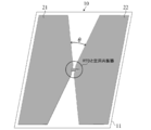
図5は、本発明に係る高出力テラヘルツ発振器10の外観斜視図であり、InPで成る半絶縁性(Semi-Insulating:SI)の基板11(1mm四方程度、高さ数μm程度)の上面に、金(Au)等の良導体で成り、ボウタイ角θの導体片21及び22で構成されるボウタイアンテナ20が配設される。ボウタイアンテナ20の導体片21及び22は線対称形であり、全体的に矩形状であり、対向する共振部に、両側に向かってそれぞれ傾斜が付けられており、導体片21及び22両者の傾斜角でボウタイ角θを形成している。また、導体片21及び22は金(Au)等の良導体で成っている。
ボウタイアンテナ20の2枚の導体片21及び22が対向する共振部には、RTD40と空洞共振器30とが配設されており、その詳細な斜視図は図6に示され、図6のY-Y’断面は図7に、Z-Z’断面は図8に、X-X’断面は図9(A)にそれぞれ示されている。空洞共振器30も金(Au)等の良導体で成っている。なお、図7及び図8では、ボウタイアンテナ20の導体片21と空洞共振器30とは、ボウタイアンテナ20の導体片21と空洞共振器30とを分かり易く識別できるように別体となっているが、実際には金(Au)等の良導体の一体構造である。いずれも同じ良導体なので、別体で接触した構造であっても良い。
図5~図8に示すように、InPで成る半絶縁性(SI)の基板11の上面に、ボウタイアンテナ20を構成する2枚の導体片21及び22がボウタイ角θで配設され、ボウタイアンテナ20の2枚の導体片21及び22の各面上に、断面矩形で長形状の2つの空洞31及び32を有する空洞共振器30が配設されている。ボウタイアンテナ20の導体片22の一部がバイアス(DC電圧)印加のための給電部22Aとなり、これに対向する空洞共振器30の一部(側面若しくは上面)がバイアス(DC電圧)印加のための給電部33となる。
図6~図8に示すように、空洞共振器30の2つの空洞31及び32は、天井の中央部から垂下する板状の壁部材34で区画されており、空洞31及び32の前面及び裏面は、本例では図9(A)に示すように両方共に開放(開口)された構造になっている。空洞共振器30の壁部材34の底部と、ボウタイアンテナ20の導体片22の上面との間には、断面矩形で長形状のRTD40が配設されており、RTD40は図9(A)に示すように空洞31及び32の前面(開放)から裏面(開放)まで延びている。また、空洞共振器30の底面と、ボウタイアンテナ20の導体片22とは、RTD40と同一の厚さ(2μm程度)の絶縁体薄膜12により分離されている。絶縁体薄膜12は空洞31の外側まで延びており、下方に屈曲して導体片21及び22を電気的に絶縁している。なお、断面L字状の絶縁体薄膜12は、SiO2などの絶縁材である。
図6及び図8に示すように、例えばボウタイアンテナ20の導体片22の空洞共振器30に近い部分には、矩形状の凹部22Bが設けられており、この凹部22B内に空洞共振器30の側面から延びたL字状の導体橋35が設けられている。導体橋35には、凹部22Bの底部に配置された、例えばInGaAsで成る安定化抵抗50(抵抗値=Rs)が接続され、安定化抵抗50は導体片22の対向する側面に接続されている。安定化抵抗50は、数ギガヘルツの寄生発振を抑圧し、安定なテラヘルツ発振を起こさせるためのものであり、導体橋35はインダクタンス(Ls)の機能を有している。この構造では、空洞共振器30の開口面と安定化抵抗50は結合して損失を生ずることはなく、このことによる出力の制限もない。
なお、凹部22Bの形状は矩形に限定されるものではなく、楕円や円形であっても良い。
バイアスが印加される給電部の1つ(22A)はボウタイアンテナ20の導体片22に印加され、導体片22を通じてRTD40の下部電極40EDとなり、他の給電部(33)は空洞共振器30の側面若しくは上面に印加され、空洞共振器30の壁部材34を通じてRTD40の上部電極40EUとなる。発振回路からの出力は、側面と底面の間の絶縁体薄膜12を通って、ボウタイアンテナ20の電極(導体片21及び22)間から放射される。絶縁体薄膜12が十分薄い(2μm程度)ので、空洞共振器30とボウタイアンテナ20の結合が小さいため、ボウタイアンテナ20の放射抵抗Raは空洞共振器30の影響を殆ど受けない。
このような構造によって、空洞共振器30とRTD40で発振回路が構成される。発振周波数は空洞共振器30のインダクタンスとRTD40のキャパシタンスで決まるが、空洞共振器30のインダクタンスが小さいため、キャパシタンスの大きなメサ面積のRTDを用いることができ、メサ面積の大きなRTD40を用いることによって高出力を実現できる。
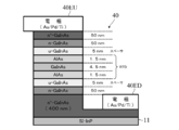
RTD40の構成例は図10であり、金(Au)、パラジウム(Pd)、チタン(Ti)の3層構造(Au/Pd/Ti)で成る2つの上部電極40EU及び下部電極40EDの間にn+-GaInAs(50nm)、n-GaInAs(50nm)、u-GaInAs(5nm)、AlAs(1.5nm)、GaInAs(4.5nm)、AlAs(1.5nm)、u-GaInAs(5nm)、n-GaInAs(50nm)、n+-GaInAs(400nm)が配設された構造である。図7及び図8に示すように、上部電極40EUは空洞共振器30の壁部材34の底部に相当し、下部電極40EDはボウタイアンテナ20の導体片22の上面に相当している。図10の最下層は、半絶縁性の基板11(SI-InP)である。
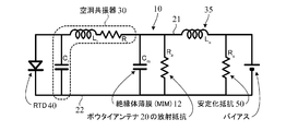
図11は本発明のテラヘルツ発振器10の等価回路を示しており、ボウタイアンテナ20の放射抵抗Raと空洞共振器30のインダクタンスLrとは独立となり、テラヘルツ発振器の発振周波数と出力のトレードオフの関係を解消することができる。
これにより、空洞共振器30はインダクタンスLrをスロットアンテナに比べて大幅に低減することができ、RTD40のキャパシタンスを小さくすることなく、発振周波数を高くすることができ、従ってメサ面積の大きな大面積RTD素子により、高出力化が可能になる。また、ボウタイアンテナ20の放射抵抗Raは空洞共振器のインダクタンスLrとは無関係になる。
これにより、空洞共振器30はインダクタンスLrをスロットアンテナに比べて大幅に低減することができ、RTD40のキャパシタンスを小さくすることなく、発振周波数を高くすることができ、従ってメサ面積の大きな大面積RTD素子により、高出力化が可能になる。また、ボウタイアンテナ20の放射抵抗Raは空洞共振器のインダクタンスLrとは無関係になる。
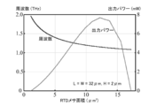
実際の構造と材料を、RTD40をInP基板11上のGaInAs/AlAsとし、電極をAu、絶縁体薄膜をSiO2と想定し、RTD40のメサ面積を可変したときの本発明のテラヘルツ発振器10のシミュレーション特性は図12であり、本例では空洞共振器30の横幅W及び奥行きLは32μmで、高さHは2μmとなっている。このシミュレーション結果からも明らかなように、周波数帯域は1.0~2.0THzであり、出力パワーは最大8mW程度が可能となっている。ボウタイアンテナ20はボウタイ角度θにより放射インピーダンスを変化させることができ、RTD40とのマッチングにより出力最大化が可能である。
上述の例では、空洞共振器30の空洞31及び32の両端が開放(短絡)であるが、図9(B)の例では、空洞共振器30の一方が塞がれている(短絡)構造である。これにより、空洞共振器30の内部には、塞いだ側(短絡側)で電界が0となる定在波が分布し、両端開放の空洞共振器(図9(A))よりも高い周波数で共振し、発振周波数が高くなる。
また、図9(C)に示すように、空洞共振器30の両端とも開放されていない両端が塞がれた(短絡)構造でも良い。この場合には、空洞共振器30の内部では、両端部で電界が0となる定在波が分布し、一方のみを塞いだ場合(図9(B))よりも一層高い周波数で共振し、発振周波数が一層高くなる。
また、上述では空洞共振器30の空洞31及び32の断面形状を矩形としているが、図13に示すような台形状としても良い。
更に上述ではボウタイアンテナ20のボウタイ角θに対して並行に、即ち導体片21及び22に平行に空洞共振器30の空洞31及び32を配置しているが、図14に示すように空洞共振器30の空洞31及び32を導体片21及び22の共振部に対して直角方向に配置しても良い。両端が開口になっている空洞共振器30の内部に、開口面と垂直に、空洞共振器30の中央部に長形状のRTD40を、一方の開口面から他方の開口面まで配置する。RTD40の上部と下部は空洞共振器30の上面内側及び底面内側にそれぞれ接続され、空洞共振器30の底面とそれ以外は、底面と側面の間に挿入された絶縁体薄膜により分離されている。
図14の構造において、電磁界シミュレータ(HFSS,Ansys)により空洞共振器30とボウタイアンテナ20のアドミタンスを求め、RTD40の特性と併せて発振特性を解析した結果、図15のような特性を得た。図15では、ボウタイ角[deg]とRTDメサ面積をパラメータとして出力パワー[mW]を得ており、ボウタイ角の最適化により、発振周波数1.5THzにおいて2mW以上の出力パワーを期待できる。
本発明の大出力テラヘルツ発振器を用いれば、テラヘルツ周波数帯に存在する物質の吸収スペクトルを測定するコンパクトなチップが実現可能になり、化学・医療におけるイメージングや分析の分野、及びテラヘルツ波による大容量無線通信の分野の一層の発展を促すことが出来ると考えられる。
1 共鳴トンネルダイオード(RTD)
2 スロットアンテナ
3 基板
4 下部電極
5 上部電極
6 安定化抵抗
10 高出力テラヘルツ発振器
11 基板(InP)
12 絶縁体薄膜
20 ボウタイアンテナ
21,22 導体片
30 空洞共振器
31,32 空洞
34 壁部材
35 導体橋
40 共鳴トンネルダイオード(RTD)
50 安定化抵抗
2 スロットアンテナ
3 基板
4 下部電極
5 上部電極
6 安定化抵抗
10 高出力テラヘルツ発振器
11 基板(InP)
12 絶縁体薄膜
20 ボウタイアンテナ
21,22 導体片
30 空洞共振器
31,32 空洞
34 壁部材
35 導体橋
40 共鳴トンネルダイオード(RTD)
50 安定化抵抗
Claims (6)
- 第1の導体片及び第2の導体片で成るボウタイアンテナが基板上に配置され、前記ボウタイアンテナの共振部に2つの空洞を有する空洞共振器が配設され、前記空洞を区画する壁部材の底部に沿って長形状の共鳴トンネルダイオードが配設された構造であり、
前記ボウタイアンテナの前記第2の導体片と、前記第1の導体片に連接された前記空洞共振器の側面若しくは上面との間にバイアスをかけることにより、前記共鳴トンネルダイオード、前記ボウタイアンテナ及び前記空洞共振器によりテラヘルツ周波数帯で発振することを特徴とする高出力テラヘルツ発振器。 - 前記共鳴トンネルダイオードの底面が前記第2の導体片の上面に接している請求項1に記載の高出力テラヘルツ発振器。
- 前記ボウタイアンテナの前記第1の導体片と前記空洞共振器とが一体的に構成されている請求項1又は2に記載の高出力テラヘルツ発振器。
- 前記ボウタイアンテナの前記第1の導体片及び前記第2の導体片、前記空洞共振器が良導体であり、前記基板が半絶縁性である請求項1乃至3のいずれかに記載の高出力テラヘルツ発振器。
- 前記ボウタイアンテナの前記第1の導体片及び前記第2の導体片の間、前記空洞共振器の底部と前記第2の導体片との間に絶縁体薄膜が配設されている請求項1乃至4のいずれかに記載の高出力テラヘルツ発振器。
- 前記ボウタイアンテナの前記第2の導体片に凹部が形成され、前記空洞共振器から延びた導体橋が前記凹部内の前記基板の上面に接続されると共に、前記導体橋と前記第2の導体片の側面との間に安定化抵抗が接続されている請求項1乃至5のいずれかに記載の高出力テラヘルツ発振器。
Priority Applications (1)
| Application Number | Priority Date | Filing Date | Title |
|---|---|---|---|
| US17/290,811 US11309834B2 (en) | 2018-11-19 | 2019-11-19 | High-power terahertz oscillator |
Applications Claiming Priority (2)
| Application Number | Priority Date | Filing Date | Title |
|---|---|---|---|
| JP2018-216285 | 2018-11-19 | ||
| JP2018216285A JP7088549B2 (ja) | 2018-11-19 | 2018-11-19 | 高出力テラヘルツ発振器 |
Publications (1)
| Publication Number | Publication Date |
|---|---|
| WO2020105627A1 true WO2020105627A1 (ja) | 2020-05-28 |
Family
ID=70774016
Family Applications (1)
| Application Number | Title | Priority Date | Filing Date |
|---|---|---|---|
| PCT/JP2019/045251 Ceased WO2020105627A1 (ja) | 2018-11-19 | 2019-11-19 | 高出力テラヘルツ発振器 |
Country Status (3)
| Country | Link |
|---|---|
| US (1) | US11309834B2 (ja) |
| JP (1) | JP7088549B2 (ja) |
| WO (1) | WO2020105627A1 (ja) |
Cited By (1)
| Publication number | Priority date | Publication date | Assignee | Title |
|---|---|---|---|---|
| CN113571998A (zh) * | 2021-06-24 | 2021-10-29 | 深圳市时代速信科技有限公司 | 一种共振隧穿二极管太赫兹振荡源 |
Families Citing this family (10)
| Publication number | Priority date | Publication date | Assignee | Title |
|---|---|---|---|---|
| CN114039201B (zh) * | 2021-11-10 | 2023-11-07 | 中国科学院上海技术物理研究所 | 一种分形蝶形太赫兹天线 |
| CN118318400A (zh) * | 2022-02-23 | 2024-07-09 | 王威智 | 太赫兹收发器及其制造方法 |
| US20230284925A1 (en) * | 2022-03-09 | 2023-09-14 | National Tsing Hua University | SCANNING BASED THz NEARFIELD IMAGING DEVICE |
| EP4475750A4 (en) * | 2022-03-10 | 2025-08-06 | Univ Nat Tsing Hua | THZ SCANNING NEAR-FIELD IMAGING DEVICE |
| US12251193B2 (en) * | 2022-03-10 | 2025-03-18 | National Tsing Hua University | Scanning based THz nearfield imaging device |
| CN118974950A (zh) | 2022-03-31 | 2024-11-15 | 索尼集团公司 | 谐振隧穿二极管和太赫兹振荡器 |
| US12273146B1 (en) * | 2023-06-01 | 2025-04-08 | Darwin Hu | Apparatus embedded with terahertz transceivers using Gunn diodes |
| US12160270B1 (en) * | 2023-06-01 | 2024-12-03 | Darwin Hu | Apparatus embedded with terahertz transceivers using resonant tunnelling diodes |
| US12308888B1 (en) * | 2023-06-01 | 2025-05-20 | Darwin Hu | Display glasses with wireless THz transceiver for bio-sensing |
| CN116878666B (zh) * | 2023-06-26 | 2025-09-05 | 之江实验室 | 太赫兹动态电感热辐射计及其制备方法及太赫兹探测系统 |
Citations (3)
| Publication number | Priority date | Publication date | Assignee | Title |
|---|---|---|---|---|
| JP2007124250A (ja) * | 2005-10-27 | 2007-05-17 | Tokyo Institute Of Technology | テラヘルツ発振素子 |
| JP2014200065A (ja) * | 2013-03-12 | 2014-10-23 | キヤノン株式会社 | 発振素子 |
| JP2017157907A (ja) * | 2016-02-29 | 2017-09-07 | 国立大学法人大阪大学 | テラヘルツ素子およびテラヘルツ集積回路 |
Family Cites Families (6)
| Publication number | Priority date | Publication date | Assignee | Title |
|---|---|---|---|---|
| US7177515B2 (en) * | 2002-03-20 | 2007-02-13 | The Regents Of The University Of Colorado | Surface plasmon devices |
| JP2006210585A (ja) | 2005-01-27 | 2006-08-10 | National Institute For Materials Science | 積層ジョセフソン接合を用いた新型テラヘルツ発振器 |
| JP2008301374A (ja) | 2007-06-01 | 2008-12-11 | Canon Inc | 発振器の製造方法、及び発振器 |
| JP5836691B2 (ja) * | 2010-09-22 | 2015-12-24 | キヤノン株式会社 | 発振器 |
| JP5686415B2 (ja) | 2012-02-21 | 2015-03-18 | 日本電信電話株式会社 | 共鳴トンネルダイオードおよびテラヘルツ発振器 |
| WO2015170425A1 (ja) | 2014-05-08 | 2015-11-12 | 国立大学法人東京工業大学 | 周波数可変テラへルツ発振器及びその製造方法 |
-
2018
- 2018-11-19 JP JP2018216285A patent/JP7088549B2/ja active Active
-
2019
- 2019-11-19 US US17/290,811 patent/US11309834B2/en active Active
- 2019-11-19 WO PCT/JP2019/045251 patent/WO2020105627A1/ja not_active Ceased
Patent Citations (3)
| Publication number | Priority date | Publication date | Assignee | Title |
|---|---|---|---|---|
| JP2007124250A (ja) * | 2005-10-27 | 2007-05-17 | Tokyo Institute Of Technology | テラヘルツ発振素子 |
| JP2014200065A (ja) * | 2013-03-12 | 2014-10-23 | キヤノン株式会社 | 発振素子 |
| JP2017157907A (ja) * | 2016-02-29 | 2017-09-07 | 国立大学法人大阪大学 | テラヘルツ素子およびテラヘルツ集積回路 |
Cited By (2)
| Publication number | Priority date | Publication date | Assignee | Title |
|---|---|---|---|---|
| CN113571998A (zh) * | 2021-06-24 | 2021-10-29 | 深圳市时代速信科技有限公司 | 一种共振隧穿二极管太赫兹振荡源 |
| CN113571998B (zh) * | 2021-06-24 | 2023-02-14 | 深圳市时代速信科技有限公司 | 一种共振隧穿二极管太赫兹振荡源 |
Also Published As
| Publication number | Publication date |
|---|---|
| JP2020088466A (ja) | 2020-06-04 |
| JP7088549B2 (ja) | 2022-06-21 |
| US20210328550A1 (en) | 2021-10-21 |
| US11309834B2 (en) | 2022-04-19 |
Similar Documents
| Publication | Publication Date | Title |
|---|---|---|
| JP7088549B2 (ja) | 高出力テラヘルツ発振器 | |
| Kasagi et al. | Large-scale array of resonant-tunneling-diode terahertz oscillators for high output power at 1 THz | |
| EP2476205B1 (en) | Oscillator having negative resistance element | |
| JP6570187B2 (ja) | 周波数可変テラヘルツ発振器及びその製造方法 | |
| JP5366663B2 (ja) | テラヘルツ発振素子 | |
| US8981859B2 (en) | Oscillator | |
| JP5808560B2 (ja) | テラヘルツ発振検出素子 | |
| Van Ta et al. | Structure dependence of oscillation characteristics of structure-simplified resonant-tunneling-diode terahertz oscillator | |
| JP2007124250A (ja) | テラヘルツ発振素子 | |
| JP5958890B2 (ja) | テラヘルツ検出素子 | |
| JP5746526B2 (ja) | テラヘルツ無線通信方式 | |
| US9899959B2 (en) | Element, and oscillator and information acquiring device including the element | |
| JP7668001B2 (ja) | テラヘルツ発振器 | |
| CN108566164B (zh) | 一种基于共振遂穿二极管的太赫兹振荡电路及振荡器 | |
| JP5648915B2 (ja) | 共鳴トンネルダイオードおよびテラヘルツ発振器 | |
| Suzuki et al. | Proposal of resonant tunneling diode oscillators with offset-fed slot antennas in terahertz and sub-terahertz range | |
| JP5417199B2 (ja) | 発振素子 | |
| Han et al. | Impedance matching method in high-power RTD THz oscillator integrated with rectangular-cavity resonator | |
| US20160036200A1 (en) | Oscillation device | |
| US9438168B2 (en) | Oscillator | |
| JP2016219796A (ja) | 素子、これを有する発振器及び情報取得装置 |
Legal Events
| Date | Code | Title | Description |
|---|---|---|---|
| 121 | Ep: the epo has been informed by wipo that ep was designated in this application |
Ref document number: 19886248 Country of ref document: EP Kind code of ref document: A1 |
|
| NENP | Non-entry into the national phase |
Ref country code: DE |
|
| 122 | Ep: pct application non-entry in european phase |
Ref document number: 19886248 Country of ref document: EP Kind code of ref document: A1 |