WO2020105145A1 - 光モジュール - Google Patents
光モジュールInfo
- Publication number
- WO2020105145A1 WO2020105145A1 PCT/JP2018/043002 JP2018043002W WO2020105145A1 WO 2020105145 A1 WO2020105145 A1 WO 2020105145A1 JP 2018043002 W JP2018043002 W JP 2018043002W WO 2020105145 A1 WO2020105145 A1 WO 2020105145A1
- Authority
- WO
- WIPO (PCT)
- Prior art keywords
- dielectric substrate
- optical module
- metal stem
- integrated device
- optical
- Prior art date
- Legal status (The legal status is an assumption and is not a legal conclusion. Google has not performed a legal analysis and makes no representation as to the accuracy of the status listed.)
- Ceased
Links
Images






Classifications
-
- H—ELECTRICITY
- H01—ELECTRIC ELEMENTS
- H01S—DEVICES USING THE PROCESS OF LIGHT AMPLIFICATION BY STIMULATED EMISSION OF RADIATION [LASER] TO AMPLIFY OR GENERATE LIGHT; DEVICES USING STIMULATED EMISSION OF ELECTROMAGNETIC RADIATION IN WAVE RANGES OTHER THAN OPTICAL
- H01S5/00—Semiconductor lasers
- H01S5/02—Structural details or components not essential to laser action
- H01S5/026—Monolithically integrated components, e.g. waveguides, monitoring photo-detectors, drivers
-
- H—ELECTRICITY
- H01—ELECTRIC ELEMENTS
- H01S—DEVICES USING THE PROCESS OF LIGHT AMPLIFICATION BY STIMULATED EMISSION OF RADIATION [LASER] TO AMPLIFY OR GENERATE LIGHT; DEVICES USING STIMULATED EMISSION OF ELECTROMAGNETIC RADIATION IN WAVE RANGES OTHER THAN OPTICAL
- H01S5/00—Semiconductor lasers
- H01S5/02—Structural details or components not essential to laser action
- H01S5/022—Mountings; Housings
- H01S5/0233—Mounting configuration of laser chips
- H01S5/02345—Wire-bonding
-
- H—ELECTRICITY
- H01—ELECTRIC ELEMENTS
- H01S—DEVICES USING THE PROCESS OF LIGHT AMPLIFICATION BY STIMULATED EMISSION OF RADIATION [LASER] TO AMPLIFY OR GENERATE LIGHT; DEVICES USING STIMULATED EMISSION OF ELECTROMAGNETIC RADIATION IN WAVE RANGES OTHER THAN OPTICAL
- H01S5/00—Semiconductor lasers
- H01S5/0014—Measuring characteristics or properties thereof
-
- H—ELECTRICITY
- H01—ELECTRIC ELEMENTS
- H01S—DEVICES USING THE PROCESS OF LIGHT AMPLIFICATION BY STIMULATED EMISSION OF RADIATION [LASER] TO AMPLIFY OR GENERATE LIGHT; DEVICES USING STIMULATED EMISSION OF ELECTROMAGNETIC RADIATION IN WAVE RANGES OTHER THAN OPTICAL
- H01S5/00—Semiconductor lasers
- H01S5/02—Structural details or components not essential to laser action
- H01S5/022—Mountings; Housings
- H01S5/023—Mount members, e.g. sub-mount members
- H01S5/0231—Stems
-
- H—ELECTRICITY
- H01—ELECTRIC ELEMENTS
- H01S—DEVICES USING THE PROCESS OF LIGHT AMPLIFICATION BY STIMULATED EMISSION OF RADIATION [LASER] TO AMPLIFY OR GENERATE LIGHT; DEVICES USING STIMULATED EMISSION OF ELECTROMAGNETIC RADIATION IN WAVE RANGES OTHER THAN OPTICAL
- H01S5/00—Semiconductor lasers
- H01S5/02—Structural details or components not essential to laser action
- H01S5/022—Mountings; Housings
- H01S5/0239—Combinations of electrical or optical elements
-
- H—ELECTRICITY
- H01—ELECTRIC ELEMENTS
- H01S—DEVICES USING THE PROCESS OF LIGHT AMPLIFICATION BY STIMULATED EMISSION OF RADIATION [LASER] TO AMPLIFY OR GENERATE LIGHT; DEVICES USING STIMULATED EMISSION OF ELECTROMAGNETIC RADIATION IN WAVE RANGES OTHER THAN OPTICAL
- H01S5/00—Semiconductor lasers
- H01S5/04—Processes or apparatus for excitation, e.g. pumping, e.g. by electron beams
- H01S5/042—Electrical excitation ; Circuits therefor
- H01S5/0425—Electrodes, e.g. characterised by the structure
- H01S5/04254—Electrodes, e.g. characterised by the structure characterised by the shape
-
- H—ELECTRICITY
- H01—ELECTRIC ELEMENTS
- H01S—DEVICES USING THE PROCESS OF LIGHT AMPLIFICATION BY STIMULATED EMISSION OF RADIATION [LASER] TO AMPLIFY OR GENERATE LIGHT; DEVICES USING STIMULATED EMISSION OF ELECTROMAGNETIC RADIATION IN WAVE RANGES OTHER THAN OPTICAL
- H01S5/00—Semiconductor lasers
- H01S5/02—Structural details or components not essential to laser action
- H01S5/024—Arrangements for thermal management
- H01S5/02469—Passive cooling, e.g. where heat is removed by the housing as a whole or by a heat pipe without any active cooling element like a TEC
-
- H—ELECTRICITY
- H01—ELECTRIC ELEMENTS
- H01S—DEVICES USING THE PROCESS OF LIGHT AMPLIFICATION BY STIMULATED EMISSION OF RADIATION [LASER] TO AMPLIFY OR GENERATE LIGHT; DEVICES USING STIMULATED EMISSION OF ELECTROMAGNETIC RADIATION IN WAVE RANGES OTHER THAN OPTICAL
- H01S5/00—Semiconductor lasers
- H01S5/02—Structural details or components not essential to laser action
- H01S5/026—Monolithically integrated components, e.g. waveguides, monitoring photo-detectors, drivers
- H01S5/0265—Intensity modulators
-
- H—ELECTRICITY
- H01—ELECTRIC ELEMENTS
- H01S—DEVICES USING THE PROCESS OF LIGHT AMPLIFICATION BY STIMULATED EMISSION OF RADIATION [LASER] TO AMPLIFY OR GENERATE LIGHT; DEVICES USING STIMULATED EMISSION OF ELECTROMAGNETIC RADIATION IN WAVE RANGES OTHER THAN OPTICAL
- H01S5/00—Semiconductor lasers
- H01S5/06—Arrangements for controlling the laser output parameters, e.g. by operating on the active medium
- H01S5/062—Arrangements for controlling the laser output parameters, e.g. by operating on the active medium by varying the potential of the electrodes
- H01S5/06226—Modulation at ultra-high frequencies
Definitions
- This application relates to an optical module.
- an optical module equipped with an EAM-LD (Electro Absorption Modulated-Laser) that integrates an electro-absorption modulator (EAM) and a semiconductor laser is used for high-speed optical communication.
- This optical module has a structure in which cooling is performed using a cooling means such as a Peltier element in order to control the temperatures of the semiconductor laser and the EAM to be constant (for example, refer to Patent Document 1 and Patent Document 2).
- a high frequency signal for modulation is applied to EAM which is an optical modulator to modulate light.
- a high frequency signal may be applied to the EAM via a bonding wire.
- impedance matching cannot be achieved at the connection point to the EAM as the frequency becomes higher.
- Patent Document 1 or Patent Document 2 which is mounted on a metal stem and uses a lead pin that coaxially penetrates the metal stem in a high frequency input portion, a line of the lead pin penetrating portion of the metal stem is used.
- the impedance becomes about 20 ⁇ to 30 ⁇ due to the restriction of the diameter of the glass holding the lead pin and the diameter of the lead pin, and it cannot match with 50 ⁇ which is a general matching resistance.
- the board on which the EAM-LD is mounted and the board for transmitting a high-frequency signal are separated, and the two are connected by a wiring member such as a wire. There is a problem of impedance mismatch even in the wire portion between the substrates.
- the high frequency signal is reflected by the EAM-LD, is reflected by the wire portion between the substrates, and is also reflected by the portion penetrating the metal stem. If the phase of the high frequency signal is rotated by 180 degrees when returning to the EAM-LD again, the gain is canceled and the band is deteriorated.
- the power for cooling is not indispensable for the generation of optical signals, so it is desired to realize a so-called uncooled optical module that can operate without cooling. It is rare. Even in the non-cooled optical module, the cooling means for controlling the temperature is not necessary, and the problem of band deterioration cannot be solved only by the non-cooled configuration.
- the substrate on which the semiconductor optical integrated device is mounted and the substrate for transmitting a high frequency signal are separated in order to minimize the heat capacity of the cooling portion. It is configured to connect between them with a wiring member such as a wire. Impedance matching is difficult in this wire portion, and this portion also serves as a reflection point, which causes deterioration of the high-frequency signal band.
- the present application discloses a technique for solving the above problems, and an object thereof is to provide a configuration that can be applied to an uncooled optical module and that suppresses band deterioration of a high-frequency signal.
- the optical module disclosed in the present application integrates a plate-shaped metal stem in which a metal lead pin is inserted into a through hole coaxially with the through hole, a high-frequency signal line connected to the lead pin, a semiconductor laser and an optical modulator. And a single dielectric substrate provided with the semiconductor optical integrated device connected to the high-frequency signal line and a bonding wire. One side surface of the dielectric substrate is perpendicular to the optical axis direction of the semiconductor optical integrated device. And the one side surface of the dielectric substrate is arranged in contact with the surface of the metal stem.
- optical module disclosed in the present application there is an effect that it can be applied to an uncooled optical module and can provide a configuration that suppresses band deterioration of high frequency signals.
- FIG. 3 is a perspective view showing the configuration of the optical module according to the first embodiment.
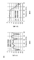
- FIG. FIG. 6 is a diagram showing characteristics of the optical module according to the first embodiment in comparison with a conventional one.
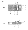
- 3A and 3B are a plan view and a side view showing a configuration of a dielectric substrate of the optical module according to the first embodiment.
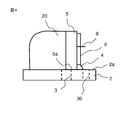
- FIG. 3 is a side view showing a main part of the optical module according to the first embodiment. It is a side view which shows the principal part of the optical module as a comparative example.
- FIG. 5 is a diagram showing characteristics of the optical module according to the first embodiment in comparison with a comparative example.
- 7A and 7B are a plan view and a side view showing a configuration of a dielectric substrate of an optical module according to a second embodiment.
- FIG. 7 is a diagram showing characteristics of the optical module according to the second embodiment in comparison with the first embodiment.
- FIG. 9 is a perspective view showing a configuration of an optical module according to a third embodiment.
- FIG. 16 is a perspective view showing the configuration of the optical module according to the fourth embodiment.
- FIG. 1 is a perspective view showing the configuration of the optical module according to the first embodiment.
- the metal stem 2 is provided with a lead pin 3 which is inserted into the through hole 30 provided in the metal stem 2 so as to be coaxial with the through hole 30.
- the lead pin 3 is fixed to the metal stem 2 via a glass material 11 provided so as to fill the through hole 30.
- the material of the metal stem 2 and the lead pin 3 may be, for example, a metal such as copper, iron, aluminum or stainless steel, and may be gold-plated or nickel-plated on the surface.
- a dielectric substrate 5 is mounted on the metal stem 2, and a semiconductor optical integrated device in which a semiconductor laser that oscillates laser light and an optical modulator that modulates the light from this semiconductor laser are integrated on the dielectric substrate 5.
- a semiconductor optical integrated device in which a semiconductor laser that oscillates laser light and an optical modulator that modulates the light from this semiconductor laser are integrated on the dielectric substrate 5.
- 9 has been implemented.
- the semiconductor optical integrated device 9 for example, an EAM-LD in which an electroabsorption type optical modulator using an InGaAsP type or AlInGaAs type quantum well absorption layer and a distributed feedback type laser diode are monolithically integrated is used.
- the semiconductor laser is not limited to the distributed feedback laser diode, and a semiconductor MZ optical modulator or the like may be used as the optical modulator.
- a substrate support portion 20 having a surface 20a perpendicular to the surface 2a of the metal stem is provided on the metal stem 2, and the dielectric substrate 5 has, for example, a back surface joined to the substrate support member 20. It is mounted along the board supporting portion 20.
- the side of the metal stem 2 on which the dielectric substrate 5 is mounted is sealed with, for example, nitrogen, but in FIG. 1, the sealing structure other than the penetrating portion of the lead pin 3 of the metal stem 2 is omitted. There is.
- the metal stem 2 is provided with a wiring introducing mechanism similar to the introduction of the lead pin 3 for introducing other signal wiring or power supply wiring. Are not directly related and are not shown.
- the semiconductor optical integrated device is mounted to minimize the heat capacity of the cooling part in order to reduce the power consumption for cooling the semiconductor optical integrated device and improve the responsiveness of temperature control.
- the circuit board and the circuit board for transmitting the high frequency signal from the lead pin were separated.
- the substrate supporting section 20 is not provided with a temperature control member for cooling the semiconductor optical integrated device 9 to control the temperature.
- a signal line for transmitting a high frequency signal from the lead pin 3 to the semiconductor optical integrated device 9 is arranged on the dielectric substrate 5 constituted by one sheet.
- the lead pin 3 is provided for inputting a high frequency signal for modulation from the flexible printed board 1 arranged on the back surface of the metal stem 2 to the side on which the dielectric substrate 5 is mounted.
- an anode electrode 6 and a cathode electrode 7 are formed on the dielectric substrate 5 as a high frequency signal line 60 on the dielectric substrate 5.
- a high frequency signal line 60 can be formed by forming a coplanar line on the entire surface of the dielectric substrate 5 while keeping the distance between the anode electrode 6 and the cathode electrode 7 constant.
- the cathode electrode 7 is electrically connected to the metal stem 2 by some method such as through holes formed in the dielectric substrate 5, castellation, or metal on the side surface of the dielectric substrate 5.
- the material of the dielectric substrate 5 for example, ceramic such as ALN or alumina may be used, or resin such as epoxy may be used.
- the dielectric substrate 5 is preferably arranged near the lead pins 3.
- One end of the lead pin 3 and one end of the anode electrode 6 on the dielectric substrate 5 are connected to each other via an adhesive 4.
- the other end of the lead pin 3 is connected to the wiring pattern of the flexible printed board 1.
- the other end of the anode electrode 6 and the semiconductor optical integrated device 9 are connected via a bonding wire 8, and the bonding wire 8 is further connected to a conductor 12 formed on the dielectric substrate 5.
- the conductor 12 is formed on the dielectric substrate 5 so as to be insulated from the cathode electrode 7, and the resistor 10 is connected between the conductor 12 and the cathode electrode 7.
- a semiconductor optical integrated device in which a semiconductor laser and an optical modulator such as an EAM-LD are integrated has a parasitic capacitance component, a parasitic resistance component, and a parasitic inductance component of a bonding wire connected to an electrode, which increases the frequency of an input signal. Therefore, impedance matching cannot be obtained.
- the matching resistance is adjusted to about 50 ⁇ in order to efficiently secure the voltage amplitude, but with this, as the frequency of the signal becomes higher, impedance matching with the lead pin penetration becomes impossible. Therefore, a part of the high frequency component of the electric signal is reflected by the semiconductor optical integrated device and returns to the driving side, and a part of the high frequency component is reflected and returned by the penetrating portion of the lead pin.
- the dielectric substrate includes a first dielectric substrate on which a high-frequency signal line for transmitting a high-frequency signal to the semiconductor optical integrated device is formed, and a second dielectric substrate on which the semiconductor optical integrated device is mounted.
- the high-frequency transmission in the configured optical module having the conventional configuration is considered as follows.
- the amplitude A of the composite wave largely depends on the reflectance and the effective electrical length of the penetrating portion of the semiconductor optical integrated device and the lead pin, and has frequency dependency.
- the lead pin 3 and the semiconductor optical integrated device 9 which is an EAM-LD are electrically connected by the anode electrode 6 and the bonding wire 8 formed on one dielectric substrate 5.
- the line impedance of the anode electrode 6 and the resistance value of the resistor 10 are values close to the characteristic impedance of the lead pin penetration portion in order to suppress multiple reflection that occurs between the semiconductor optical integrated device 9 and the lead pin penetration portion. Is preferred.
- a photodetector such as a photodiode (PD) for detecting laser light leaking from the back surface of the semiconductor optical integrated device 9 between the semiconductor optical integrated device 9 and the metal stem 2. It is configured to arrange vessels.
- the photodetector is not arranged as shown in FIG. 1, but the rear surface of the semiconductor optical integrated device 9 and the surface 2a of the metal stem are arranged as close as possible, The height of the dielectric substrate 5 is lowered and the length of the anode electrode 6 is shortened. This also makes it possible to suppress the gain deterioration in the high frequency band.
- the optical module may be controlled by ACC (Auto Current Control) by controlling the driving current of the semiconductor laser, or the optical modulator may be an electroabsorption type optical modulator ( In the case of EAM), the photocurrent generated at the time of modulation may be monitored, and the photocurrent may be used as a feedback control signal, for example, and may be driven by APC (Auto Power Control).
- ACC Auto Current Control
- the optical modulator may be an electroabsorption type optical modulator ( In the case of EAM)
- the photocurrent generated at the time of modulation may be monitored, and the photocurrent may be used as a feedback control signal, for example, and may be driven by APC (Auto Power Control).
- a dielectric substrate is divided into a first dielectric substrate and a second dielectric substrate, and the frequency characteristics of an optical module having a conventional configuration in which the dielectric substrates are connected by wires.
- An example (broken line) and a frequency characteristic example (solid line) of the optical module according to the first embodiment having a configuration in which one dielectric substrate is used and there is no wire connection between the dielectric substrates are shown. It can be seen that both the S parameter S11 (FIG. 2A), which is the reflection characteristic of high-frequency transmission, and the S21 (FIG. 2B), which is the transmission characteristic, are improved in the optical module according to the first embodiment.
- FIG. 3A is a plan view of the dielectric substrate 5 shown in FIG. 1 viewed from the substrate surface side
- FIG. 3B shows one side surface 5a of the dielectric substrate 5 in contact with the surface 2a of the metal stem.
- 6 is a side view of the substrate 5.
- FIG. One side surface 5a of the dielectric substrate 5 extends in a direction perpendicular to the optical axis direction La of the semiconductor optical integrated device 9. Therefore, by arranging the dielectric substrate 5 along the substrate supporting portion 20 and arranging the one side surface 5a of the dielectric substrate 5 so as to be in contact with the surface 2a of the metal stem, the optical axis direction La of the semiconductor optical integrated device 9 can be adjusted. Since it is set in the direction perpendicular to the surface 2a of the metal stem, it becomes easy to adjust the optical axis direction.
- FIG. 4 is an enlarged side view showing a portion where the dielectric substrate 5 is mounted.
- a cathode electrode 7 is formed except for a portion corresponding to a portion where the anode electrode 6 is formed on the surface.
- the cathode electrode 7 formed on the one side surface 5a of the dielectric substrate 5 on the metal stem surface 2a. And the cathode electrode 7 can be directly grounded to the metal stem 2.
- the high-frequency signal line connected to the lead pin 3 penetrating the metal stem 2 and the semiconductor optical integrated device 9 in which the semiconductor laser and the optical modulator are integrated are provided as one sheet. Since it is arranged on the dielectric substrate 5 and one side surface 5a of the dielectric substrate 5 is arranged so as to be in contact with the surface 2a of the metal stem, it can be applied to an uncooled optical module and has a wide range of high frequency characteristics.
- the optical module can easily adjust the optical axis.
- FIG. 7A is a plan view showing the structure of the dielectric substrate 5 of the optical module according to the second embodiment, as seen from the surface of the dielectric substrate 5, and FIG. 7B is a side view as seen from the side of the metal stem 2 of the dielectric substrate 5.
- a groove 13 is provided on the surface of the dielectric substrate 5, and the semiconductor optical integrated device 9 is mounted in this groove 13.
- FIG. 9 is a perspective view showing the configuration of the optical module according to the third embodiment.
- the photodetector is not provided in the first embodiment, the provision of the photodetector facilitates stabilization of the optical output.
- the third embodiment is an embodiment in which the photodetector 15 is provided.
- a photodetector is not provided on the dielectric substrate 5, but a groove 14 is provided on the surface 2a of the metal stem 2, and the photodetector 15 which is a photodetector 15 is provided on the groove 14.
- the diode is mounted.
- the dielectric substrate 5 does not increase in size, and therefore, the length of the anode electrode does not increase, and leaks to the back surface of the semiconductor optical integrated device 9 while suppressing band degradation. It becomes possible to detect the back light.
- the APC Auto Power Control
- the bottom surface of the groove 14 in which the photodetector 15 such as a photodiode is installed is inclined with respect to the surface 2a of the metal stem because the back light reflected by the photodetector 15 is again in the semiconductor optical integrated device 9. This is to prevent the reflected light from returning to the semiconductor optical integrated device 9 so as not to affect the operation of the semiconductor optical integrated device 9 by returning to the above.
- FIG. 10 is a perspective view showing the configuration of the optical module according to the fourth embodiment.
- the groove 14 is provided in the surface 2a of the metal stem 2 so that the dimension of the dielectric substrate 5 in the optical axis direction does not become large, and the photodetector 15 such as a photodiode is mounted in the groove 14.
- the dimension of the dielectric substrate 5 in the optical axis direction is slightly larger, but as shown in FIG. 10, a little space is provided in the portion of the dielectric substrate 5 which is the back surface of the semiconductor optical integrated device 9. Then, the photodetector 15 is mounted on the dielectric substrate 5.
- the fourth embodiment similarly to the third embodiment, it is desirable to install the light detector 15 in any direction so that the reflected light from the photodetector 15 does not return to the semiconductor optical integrated device 9. Also with this configuration, by using the output of the photodetector 15 that detects the back light of the semiconductor optical integrated device 9, the APC driving of the optical module becomes easy.
Landscapes
- Physics & Mathematics (AREA)
- Condensed Matter Physics & Semiconductors (AREA)
- General Physics & Mathematics (AREA)
- Electromagnetism (AREA)
- Optics & Photonics (AREA)
- Semiconductor Lasers (AREA)
Abstract
本願に開示される光モジュールは、貫通孔(30)に金属製のリードピン(3)が貫通孔(30)と同軸に挿入された板状の金属ステム(2)と、リードピン(2)に接続される高周波信号線路(60)と、半導体レーザーと光変調器が集積され、高周波信号線路(60)とボンディングワイヤ(8)で接続された半導体光集積素子(9)とが備えられた一枚の誘電体基板(5)とを備え、誘電体基板(5)の一側面(5a)は半導体光集積素子(9)の光軸方向(La)と垂直な方向に延在しており、誘電体基板(5)は一側面(5a)が金属ステム(2)の表面(2a)に接して配置されている。
Description
本願は、光モジュールに関する。
現在、電界吸収型光変調器(Electro-absorption Modulator:EAM)と半導体レーザーが集積されたEAM-LD(Electro Absorption Modulated-Laser)を搭載する光モジュールが、高速の光通信に用いられている。この光モジュールは、半導体レーザーおよびEAMの温度が一定となるよう制御するため、ペルチェ素子などの冷却手段を用いて冷却する構造になっている(例えば特許文献1および特許文献2参照)。
EAM-LDの場合、光変調器であるEAMに変調用の高周波信号を印加して光を変調する。EAMへは高周波信号がボンディングワイヤを介して印加される場合がある。この場合、EAMにおける寄生容量あるいは寄生抵抗、ボンディングワイヤのインダクタンス等の影響により、周波数が高くなるにつれ、EAMへの接続点においてインピーダンス整合が取れなくなる。
特許文献1あるいは特許文献2に開示されている、金属ステムに搭載され、高周波の入力部に金属ステムを同軸状に貫通するリードピンを用いた構成にあっては、金属ステムのリードピン貫通部の線路インピーダンスが、リードピンを保持するガラス径とリードピン径の制約により、20Ω~30Ω程度になり、整合抵抗として一般的な50Ωとは整合が取れない。また、EAM-LDを搭載する基板と、高周波の信号を伝送するための基板とが分かれており、その間をワイヤなどの配線部材で接続する構成となっている。この、基板間のワイヤの部分でもインピーダンス不整合の問題がある。以上のように、信号の周波数が高くなるに従い、インピーダンスの不整合のため、高周波信号がEAM-LDで反射し、基板間のワイヤ部分でも反射し、さらに金属ステムを貫通する部分でも反射して再びEAM-LDに戻ってきたときに高周波信号の位相が180度回っていると利得を打ち消してしまい、帯域劣化を起こす。
一方、従来の冷却手段を用いた光モジュールにおいて、冷却するための電力は、光信号発生にとって必須の電力ではないため、冷却せずに動作が可能な、いわゆる非冷却の光モジュールの実現が望まれている。非冷却の光モジュールにおいても、温度制御のための冷却手段が不要なだけであり、非冷却の構成であるというだけでは、帯域劣化の問題が解消されるものではない。
従来の、冷却手段を用いた光モジュールにおいては、以上のように、冷却部分の熱容量をできるだけ小さくするため、半導体光集積素子を搭載する基板と、高周波の信号を伝送するための基板とが分かれており、その間をワイヤなどの配線部材で接続する構成がとられている。このワイヤの部分におけるインピーダンス整合が難しく、この部分も反射点となり、高周波信号の帯域劣化の原因となる。
本願は、上記のような課題を解決するための技術を開示するものであり、非冷却の光モジュールに適用可能な、高周波信号の帯域劣化を抑える構成を提供することを目的とする。
本願に開示される光モジュールは、貫通孔に金属製のリードピンが貫通孔と同軸に挿入された板状の金属ステムと、リードピンに接続される高周波信号線路と、半導体レーザーと光変調器が集積され、高周波信号線路とボンディングワイヤで接続された半導体光集積素子とが備えられた一枚の誘電体基板とを備え、誘電体基板の一側面は半導体光集積素子の光軸方向と垂直な方向に延在しており、誘電体基板は一側面が前記金属ステムの表面に接して配置されているものである。
本願に開示される光モジュールによれば、非冷却の光モジュールに適用可能で、高周波信号の帯域劣化を抑える構成を提供することができる効果がある。
図1は実施の形態1による光モジュールの構成を示す斜視図である。図1において、金属ステム2には、金属ステム2に設けられた貫通孔30に、貫通孔30と同軸に挿入されたリードピン3が設けられている。リードピン3は貫通孔30を埋めるように設けられたガラス材11を介して金属ステム2に固定されている。金属ステム2およびリードピン3の材料は、例えば、銅、鉄、アルミニウムまたはステンレスなどの金属を用いることができ、金メッキまたはニッケルメッキなどを表面に施すようにしてもよい。
金属ステム2には、誘電体基板5が実装され、誘電体基板5上には、レーザー光を発振する半導体レーザーとこの半導体レーザーからの光を変調する光変調器が集積された半導体光集積素子9が実装されている。半導体光集積素子9としては、例えば、InGaAsP系あるいはAlInGaAs系量子井戸吸収層を用いた電界吸収型光変調器と分布帰還型レーザーダイオードとをモノリシックに集積したEAM-LDを用いる。半導体レーザーは分布帰還型レーザーダイオードに限らず、また光変調器としては、半導体MZ光変調器などを用いるようにしてもよい。金属ステム2上には、金属ステムの表面2aに対して垂直な面20aを有する基板支持部20が設けられており、誘電体基板5は、例えば裏面が基板支持部材20に接合されるなど、この基板支持部20に沿って実装されている。なお、金属ステム2の誘電体基板5が実装されている側は、例えば窒素などで封止されるが、図1では金属ステム2のリードピン3の貫通部以外の封止の構造は省略している。また、金属ステム2には、高周波信号を導入するリードピン3以外にも、他の信号配線あるいは電源供給配線などを導入するため、リードピン3の導入と類似の配線導入機構が設けられるが、本願とは直接関係ないため図示を省略している。
従来の冷却型の光モジュールでは、半導体光集積素子を冷却するための消費電力を少なくし、温度制御の応答性を良くするため、冷却部分の熱容量をできるだけ小さくするよう、半導体光集積素子を搭載する基板と、リードピンからの高周波の信号を伝送するための基板とが分かれていた。しかし、温度制御をしない、非冷却の光モジュールでは、冷却部分の熱容量をできるだけ小さくするという制約条件がない。図1の光モジュールにおいては、基板支持部20には、半導体光集積素子9を冷却して温度制御する温度制御部材を設けていない。一枚で構成される誘電体基板5上には、半導体光集積素子9だけではなく、リードピン3から、半導体光集積素子9に高周波信号を伝送する信号線路も配置されている。リードピン3は、変調のための高周波信号を、金属ステム2の裏面に配置されているフレキシブルプリント基板1から誘電体基板5が実装されている側に入力するために設けられている。リードピン3から高周波信号を伝送するため、誘電体基板5上の高周波信号線路60として、誘電体基板5上にアノード電極6とカソード電極7が形成されている。アノード電極6とカソード電極7との間隔を一定に保った状態で誘電体基板5上の全面に形成してコプレナ線路を構成し、高周波信号線路60とすることができる。また、カソード電極7は、誘電体基板5に形成されたスルーホール、キャスタレーションあるいは、誘電体基板5の側面のメタルを介するなど、なんらかの方法により金属ステム2と電気的に接続する。
誘電体基板5の材料は、例えば、ALNあるいはアルミナなどのセラミックを用いるようにしてもよいし、エポキシなどの樹脂を用いるようにしてもよい。なお、誘電体基板5は、リードピン3の近傍に配置することが好ましい。
リードピン3の一端と誘電体基板5上のアノード電極6の一端とは接着剤4を介して互いに接続されている。リードピン3の他端はフレキシブルプリント基板1の配線パターンと接続されている。アノード電極6の他端と半導体光集積素子9はボンディングワイヤ8を介し接続され、ボンディングワイヤ8は、さらに誘電体基板5上に形成されている導体12に接続されている。導体12は、誘電体基板5上にカソード電極7とは絶縁されて形成されており、導体12とカソード電極7との間には抵抗体10が接続されている。
次に動作について説明する。EAM-LDなど半導体レーザーと光変調器が集積された半導体光集積素子には寄生容量成分、寄生抵抗成分、電極と接続するボンディングワイヤの寄生インダクタンス成分が存在し、入力信号の周波数が高くなるにしたがって、インピーダンス整合が取れなくなる。一方、リードピンの貫通部は、気密性および信頼性の観点からリード径がΦ0.3~0.4mm、ガラス径がΦ0.7~0.8mm程度、ガラスの比誘電率εr=5.5~7.0程度であり、インピーダンスにすると、20~30Ωとなる。
一般的に、整合抵抗は電圧振幅を効率的に確保するために50Ω程度に合わせるが、これでは、信号の周波数が高くなるにつれ、リードピンの貫通部とのインピーダンス整合が取れなくなる。そのため、電気信号の高周波成分は半導体光集積素子で一部が反射して駆動側に戻り、リードピンの貫通部でまた一部が反射して戻ってくる。
進行波をY0として振幅を規格化すると次式であらわされる。
Y0=sin(ωt)
誘電体基板が、半導体光集積素子に高周波信号を伝送するための高周波信号線路が形成されている第1の誘電体基板と、半導体光集積素子が搭載されている第2の誘電体基板とで構成されている、従来の構成の光モジュールにおける高周波伝送は以下のように考えられる。半導体光集積素子、半導体光集積素子と第2の誘電体基板を接続するボンディングワイヤ、第1の誘電体基板と第2の誘電体基板を接続するボンディングワイヤ、リードピンの貫通部での反射率をそれぞれρ1、ρ2、ρ3、ρ4とすると、反射波Y1は、
Y1=ρ1xρ2xρ3xρ4xsin(ωt-Φ)
とあらわせ、合成波Y2は
Y2=Y0+Y1
=sin(ωt)+ρ1xρ2xρ3xρ4xsin(ωt-Φ)
=Axsin(ωt+Θ)
とあらわせる。ただし、
A=[{1+ρ1xρ2xρ3xρ4xcos(Φ)}2+
{ρ1xρ2xρ3xρ4xsin(Φ)}2]1/2
TanΘ=-{ρ1xρ2xρ3xρ4xsin(Φ)}/
{1+ρ1xρ2xρ3xρ4xcos(Φ)}
となる。
Y0=sin(ωt)
誘電体基板が、半導体光集積素子に高周波信号を伝送するための高周波信号線路が形成されている第1の誘電体基板と、半導体光集積素子が搭載されている第2の誘電体基板とで構成されている、従来の構成の光モジュールにおける高周波伝送は以下のように考えられる。半導体光集積素子、半導体光集積素子と第2の誘電体基板を接続するボンディングワイヤ、第1の誘電体基板と第2の誘電体基板を接続するボンディングワイヤ、リードピンの貫通部での反射率をそれぞれρ1、ρ2、ρ3、ρ4とすると、反射波Y1は、
Y1=ρ1xρ2xρ3xρ4xsin(ωt-Φ)
とあらわせ、合成波Y2は
Y2=Y0+Y1
=sin(ωt)+ρ1xρ2xρ3xρ4xsin(ωt-Φ)
=Axsin(ωt+Θ)
とあらわせる。ただし、
A=[{1+ρ1xρ2xρ3xρ4xcos(Φ)}2+
{ρ1xρ2xρ3xρ4xsin(Φ)}2]1/2
TanΘ=-{ρ1xρ2xρ3xρ4xsin(Φ)}/
{1+ρ1xρ2xρ3xρ4xcos(Φ)}
となる。
また、反射波の位相Φは、半導体光集積素子からリードピンの貫通部までの長さをL、周波数をf、伝送路中の信号速度をc'とすると、
Φ=2Lx(f/c' )x 2π
とあらわせる。
Φ=2Lx(f/c' )x 2π
とあらわせる。
上記の式から、合成波の振幅Aは、反射率と、半導体光集積素子とリードピンの貫通部の実効的な電気長に大きく依存し、周波数依存性を持つことが分かる。
単に遮断周波数を広帯域化させるという観点では、リードピンの貫通部の特性インピーダンスに整合回路および線路のインピーダンスを整合させるのが好ましい。リードピンの貫通部の特性インピーダンスを50Ωに整合させるためには、一般的にリード-金属ステム間の充填材料を、比誘電率が1.8~2.8の誘電体とするか、あるいは、充填材料が、一般的に用いられているガラス材(εr=5.5~7.0)であれば、リード径とガラス径の比を7.2~9.2とする必要がある。
実施の形態1の光モジュールでは、1枚の誘電体基板5上に形成したアノード電極6とボンディングワイヤ8にて、リードピン3とEAM-LDである半導体光集積素子9を電気的に接続し、従来存在していた第1の誘電体基板と第2の誘電体基板を接続するボンディングワイヤが存在しない。したがって、第1の誘電体基板と第2の誘電体基板を接続するボンディングワイヤでの反射率ρ3の影響を無効化することができ、高い周波数帯域での利得の劣化を従来よりも抑制することができる。
このとき、アノード電極6の線路インピーダンス、および抵抗体10の抵抗値は、半導体光集積素子9とリードピンの貫通部の間で生じる多重反射を抑制するため、リードピンの貫通部の特性インピーダンスに近い値にするのが好ましい。
一般的に、光モジュールでは、光出力をモニタするため、半導体光集積素子9と金属ステム2の間に半導体光集積素子9の背面から漏れるレーザー光を検知するフォトダイオード(PD)などの光検出器を配置する構成がとられる。本実施の形態1による光モジュールでは、図1に示すように光検出器を配置せず、半導体光集積素子9の背面と金属ステムの表面2aとの間隔をできるだけ近くなるよう配置することで、誘電体基板5の高さを低くし、アノード電極6の長さを短くしている。これによっても、高い周波数帯域での利得の劣化を抑制することができる。
なお、光検出器を設けない場合、光モジュールの制御方法としては、半導体レーザーの駆動電流制御によるACC(Auto Current Control)で駆動してもよいし、光変調器が電界吸収型光変調器(EAM)である場合、変調時に生じる光電流をモニタリングし、例えば光電流をフィードバック制御の信号に用いるなど、APC(Auto Power Control)で駆動してもよい。
図2Aおよび図2Bに、誘電体基板が第1の誘電体基板と第2の誘電体基板の2枚に分かれており、誘電体基板間をワイヤで接続する従来の構成の光モジュールの周波数特性例(破線)と、誘電体基板を1枚として、誘電体基板間のワイヤ接続が無い構成である実施の形態1による光モジュールの周波数特性例(実線)を示す。高周波伝送の反射特性であるSパラメータS11(図2A)、および透過特性であるS21(図2B)共に実施の形態1による光モジュールにおいて特性が改善されていることがわかる。
図3Aは、図1に示す誘電体基板5を基板表面側から見た平面図、図3Bは、金属ステムの表面2aに接している誘電体基板5の一側面5aの側を示す、誘電体基板5の側面図である。誘電体基板5の一側面5aは、半導体光集積素子9の光軸方向Laに垂直な方向に延在している。したがって、誘電体基板5を基板支持部20に沿わせるとともに、誘電体基板5の一側面5aを金属ステムの表面2aに接するように配置することで、半導体光集積素子9の光軸方向Laが金属ステムの表面2aに対して垂直な方向に設定されるため、光軸方向の調整が容易となる。
図4は、誘電体基板5が実装されている部分を拡大して示す側面図である。図3に示すように、誘電体基板5の一側面5aには、表面にアノード電極6が形成されている部分に対応する部分を除いて、カソード電極7が形成されている。図4に示すように、一側面5aを金属ステムの表面2aに接するよう誘電体基板5を配置することにより、金属ステム表面2aに誘電体基板5の一側面5aに形成されているカソード電極7を接合して、カソード電極7を金属ステム2に直接接地することができる。この構成により、信号線路となるリード部に対しAC-GNDが近くなるため、リード部のインダクタンス成分が低減され、光モジュールの広帯域化が可能となる。図6Aおよび図6Bに、図4に示す、誘電体基板5の一側面5aに形成されたカソード電極7が金属ステムの表面2aに直接接地された場合(実線)と、図5に示す側面図のように、誘電体基板5の一側面5aと金属ステムの表面2aが離れて配置され、カソード電極7が金属ステムの表面2aに直接接地されない場合(破線)の周波数特性を示す。直接接地された場合、若干ではあるが周波数特性が改善されていることがわかる。
以上のように、実施の形態1による光モジュールでは、金属ステム2を貫通するリードピン3に接続される高周波信号線路と、半導体レーザーと光変調器が集積された半導体光集積素子9を一枚の誘電体基板5に配置し、誘電体基板5の一側面5aが金属ステムの表面2aに接して配置するようにしたので、非冷却の光モジュールに適用可能で、高周波特性が広帯域であるとともに、光軸の調整が容易な光モジュールとすることができる。
実施の形態2.
図7Aは、実施の形態2による光モジュールの誘電体基板5の構成を示す、誘電体基板5を表面から見た平面図、図7Bは誘電体基板5の金属ステム2側から見た側面図である。図7Aおよび図7Bに示すように、誘電体基板5表面に溝13を設け、この溝13に半導体光集積素子9を実装している。この構成により、アノード電極6-半導体光集積素子9-導体12間のボンディングワイヤ8を短尺化でき、ワイヤインダクタンスが低減され、光モジュールの広帯域化が可能となる。図8Aおよび図8Bに、溝13を設けない実施の形態1による光モジュールと、溝13を設けてボンディングワイヤ8を短尺化した光モジュールの周波数特性を示す。溝13を設けてボンディングワイヤ8を短尺化することにより、Sパラメータのうち、特に透過特性であるS21がより高周波まで伸び、広帯域化されているのがわかる。
図7Aは、実施の形態2による光モジュールの誘電体基板5の構成を示す、誘電体基板5を表面から見た平面図、図7Bは誘電体基板5の金属ステム2側から見た側面図である。図7Aおよび図7Bに示すように、誘電体基板5表面に溝13を設け、この溝13に半導体光集積素子9を実装している。この構成により、アノード電極6-半導体光集積素子9-導体12間のボンディングワイヤ8を短尺化でき、ワイヤインダクタンスが低減され、光モジュールの広帯域化が可能となる。図8Aおよび図8Bに、溝13を設けない実施の形態1による光モジュールと、溝13を設けてボンディングワイヤ8を短尺化した光モジュールの周波数特性を示す。溝13を設けてボンディングワイヤ8を短尺化することにより、Sパラメータのうち、特に透過特性であるS21がより高周波まで伸び、広帯域化されているのがわかる。
実施の形態3.
図9は、実施の形態3による光モジュールの構成を示す斜視図である。実施の形態1では、光検出器を設けなかったが、光検出器を設けることにより光出力の安定化が容易となる。本実施の形態3は、光検出器15を設ける実施の形態である。誘電体基板5の光軸方向の寸法を小さくするため、光検出器を誘電体基板5に設けず、金属ステム2の表面2aに溝14を設け、この溝14に光検出器15であるフォトダイオードを実装している。溝14に光検出器15を設けることにより、誘電体基板5を大きくすること無く、したがってアノード電極の長さも長くすること無く、帯域劣化を抑えたまま、半導体光集積素子9の背面に漏れ出る背面光を検知することが可能となる。背面光を検知した光検出器15の出力を用いることで、光モジュールのAPC(Auto Power Control)駆動が容易となる。なお、フォトダイオードなどの光検出器15を設置する溝14の底面を、金属ステムの表面2aに対して傾けているのは、光検出器15で反射された背面光が再び半導体光集積素子9に戻って半導体光集積素子9の動作に影響することがないよう、反射光が半導体光集積素子9に戻らないようにするためである。
図9は、実施の形態3による光モジュールの構成を示す斜視図である。実施の形態1では、光検出器を設けなかったが、光検出器を設けることにより光出力の安定化が容易となる。本実施の形態3は、光検出器15を設ける実施の形態である。誘電体基板5の光軸方向の寸法を小さくするため、光検出器を誘電体基板5に設けず、金属ステム2の表面2aに溝14を設け、この溝14に光検出器15であるフォトダイオードを実装している。溝14に光検出器15を設けることにより、誘電体基板5を大きくすること無く、したがってアノード電極の長さも長くすること無く、帯域劣化を抑えたまま、半導体光集積素子9の背面に漏れ出る背面光を検知することが可能となる。背面光を検知した光検出器15の出力を用いることで、光モジュールのAPC(Auto Power Control)駆動が容易となる。なお、フォトダイオードなどの光検出器15を設置する溝14の底面を、金属ステムの表面2aに対して傾けているのは、光検出器15で反射された背面光が再び半導体光集積素子9に戻って半導体光集積素子9の動作に影響することがないよう、反射光が半導体光集積素子9に戻らないようにするためである。
実施の形態4.
図10は、実施の形態4による光モジュールの構成を示す斜視図である。実施の形態3では、誘電体基板5の光軸方向の寸法が大きくならないよう、金属ステム2の表面2aに溝14を設け、この溝14にフォトダイオードなどの光検出器15を実装した。本実施の形態4では、誘電体基板5の光軸方向の寸法は若干大きくなるが、図10に示すように、誘電体基板5の半導体光集積素子9の背面となる部分に少しスペースを設けて、光検出器15を誘電体基板5上に実装している。本実施の形態4においても、実施の形態3と同様、光検出器15からの反射光が半導体光集積素子9に戻らないよう、いずれかの方向に傾けて設置することが望ましい。この構成によっても、半導体光集積素子9の背面光を検知する光検出器15の出力を用いることで、光モジュールのAPC駆動が容易となる。
図10は、実施の形態4による光モジュールの構成を示す斜視図である。実施の形態3では、誘電体基板5の光軸方向の寸法が大きくならないよう、金属ステム2の表面2aに溝14を設け、この溝14にフォトダイオードなどの光検出器15を実装した。本実施の形態4では、誘電体基板5の光軸方向の寸法は若干大きくなるが、図10に示すように、誘電体基板5の半導体光集積素子9の背面となる部分に少しスペースを設けて、光検出器15を誘電体基板5上に実装している。本実施の形態4においても、実施の形態3と同様、光検出器15からの反射光が半導体光集積素子9に戻らないよう、いずれかの方向に傾けて設置することが望ましい。この構成によっても、半導体光集積素子9の背面光を検知する光検出器15の出力を用いることで、光モジュールのAPC駆動が容易となる。
本願には、様々な例示的な実施の形態及び実施例が記載されているが、1つ、または複数の実施の形態に記載された様々な特徴、態様、及び機能は特定の実施の形態の適用に限られるのではなく、単独で、または様々な組み合わせで実施の形態に適用可能である。従って、例示されていない無数の変形例が、本願明細書に開示される技術の範囲内において想定される。例えば、少なくとも1つの構成要素を変形する場合、追加する場合または省略する場合、さらには、少なくとも1つの構成要素を抽出し、他の実施の形態の構成要素と組み合わせる場合が含まれるものとする。
2 金属ステム、2a 金属ステムの表面、3 リードピン、5 誘電体基板、7 カソード電極、8 ボンディングワイヤ、9 半導体光集積素子、13 (誘電体基板の)溝、14 (金属ステムの表面の)溝、15 光検出器、20 基板支持部、30 貫通孔、60 高周波信号線路
Claims (6)
- 貫通孔に金属製のリードピンが前記貫通孔と同軸に挿入された板状の金属ステムと、
前記リードピンに接続される高周波信号線路と、半導体レーザーと光変調器が集積され、前記高周波信号線路とボンディングワイヤで接続された半導体光集積素子とが備えられた一枚の誘電体基板と、
を備え、
前記誘電体基板の一側面は前記半導体光集積素子の光軸方向と垂直な方向に延在しており、前記誘電体基板は前記一側面が前記金属ステムの表面に接して配置されていることを特徴とする光モジュール。 - 前記一側面の少なくとも一部には、前記高周波信号線路のカソード電極と共通の電極が形成されており、当該電極と前記金属ステムの表面とが電気接続されていることを特徴とする請求項1に記載の光モジュール。
- 前記金属ステムの表面に、前記金属ステムの表面に対して垂直となる垂直面を有し、温度制御部材を設けない基板支持部を備え、前記誘電体基板は、裏面が前記基板支持部の前記垂直面に沿って配置されていることを特徴とする請求項1または2に記載の光モジュール。
- 前記半導体光集積素子は、前記誘電体基板の表面に設けられた溝内に配置されていることを特徴とする請求項1から3のいずれか1項に記載の光モジュール。
- 前記半導体光集積素子は、光出力の背面が前記金属ステムの側であり、前記半導体光集積素子の背面に漏れる光を検出する光検出器が、前記金属ステムの表面に設けられた溝に配置されていることを特徴とする請求項1から4のいずれか1項に記載の光モジュール。
- 前記半導体光集積素子は、光出力の背面が前記金属ステムの側であり、前記半導体光集積素子の背面に漏れる光を検出する光検出器が、前記誘電体基板に配置されていることを特徴とする請求項1から4のいずれか1項に記載の光モジュール。
Priority Applications (5)
| Application Number | Priority Date | Filing Date | Title |
|---|---|---|---|
| PCT/JP2018/043002 WO2020105145A1 (ja) | 2018-11-21 | 2018-11-21 | 光モジュール |
| US17/275,048 US12015242B2 (en) | 2018-11-21 | 2018-11-21 | Optical module |
| CN201880098516.0A CN112997371B (zh) | 2018-11-21 | 2018-11-21 | 光模块 |
| JP2020557083A JP7019838B2 (ja) | 2018-11-21 | 2018-11-21 | 光モジュール |
| TW108139218A TWI735995B (zh) | 2018-11-21 | 2019-10-30 | 光模組 |
Applications Claiming Priority (1)
| Application Number | Priority Date | Filing Date | Title |
|---|---|---|---|
| PCT/JP2018/043002 WO2020105145A1 (ja) | 2018-11-21 | 2018-11-21 | 光モジュール |
Publications (1)
| Publication Number | Publication Date |
|---|---|
| WO2020105145A1 true WO2020105145A1 (ja) | 2020-05-28 |
Family
ID=70774703
Family Applications (1)
| Application Number | Title | Priority Date | Filing Date |
|---|---|---|---|
| PCT/JP2018/043002 Ceased WO2020105145A1 (ja) | 2018-11-21 | 2018-11-21 | 光モジュール |
Country Status (5)
| Country | Link |
|---|---|
| US (1) | US12015242B2 (ja) |
| JP (1) | JP7019838B2 (ja) |
| CN (1) | CN112997371B (ja) |
| TW (1) | TWI735995B (ja) |
| WO (1) | WO2020105145A1 (ja) |
Families Citing this family (3)
| Publication number | Priority date | Publication date | Assignee | Title |
|---|---|---|---|---|
| US12126138B2 (en) * | 2020-10-13 | 2024-10-22 | Lumentum Japan, Inc. | Optical semiconductor device and semiconductor light-emitting device |
| JP7571975B2 (ja) | 2021-06-29 | 2024-10-23 | 新光電気工業株式会社 | 半導体パッケージ用ステム、半導体パッケージ |
| CN119487713A (zh) * | 2022-07-19 | 2025-02-18 | 三菱电机株式会社 | 半导体激光光源装置 |
Citations (6)
| Publication number | Priority date | Publication date | Assignee | Title |
|---|---|---|---|---|
| US20050105911A1 (en) * | 2003-11-14 | 2005-05-19 | Yong-Chan Keh | TO-can type optical module |
| JP2007059692A (ja) * | 2005-08-25 | 2007-03-08 | Sumitomo Electric Ind Ltd | 光モジュール |
| JP2010135687A (ja) * | 2008-12-08 | 2010-06-17 | Sumitomo Electric Ind Ltd | 光モジュール |
| WO2010140473A1 (ja) * | 2009-06-02 | 2010-12-09 | 三菱電機株式会社 | 半導体光変調装置 |
| JP2011197360A (ja) * | 2010-03-19 | 2011-10-06 | Mitsubishi Electric Corp | 半導体光変調装置 |
| JP2016225457A (ja) * | 2015-05-29 | 2016-12-28 | 新光電気工業株式会社 | 半導体装置用ステム及び半導体装置 |
Family Cites Families (16)
| Publication number | Priority date | Publication date | Assignee | Title |
|---|---|---|---|---|
| JP2001135748A (ja) * | 1999-11-10 | 2001-05-18 | Hitachi Ltd | 高周波用光半導体実装基板 |
| JP4617636B2 (ja) * | 2003-03-19 | 2011-01-26 | 住友電気工業株式会社 | 光モジュール |
| JP2004363242A (ja) * | 2003-06-03 | 2004-12-24 | Sumitomo Electric Ind Ltd | 光モジュール |
| JP4058764B2 (ja) * | 2003-06-26 | 2008-03-12 | 住友電気工業株式会社 | 通信モジュール |
| JP4393187B2 (ja) | 2003-12-26 | 2010-01-06 | 日本オプネクスト株式会社 | 半導体光素子用チップキャリア、光モジュール、及び光送受信器 |
| JP3990674B2 (ja) * | 2004-02-10 | 2007-10-17 | 日本オプネクスト株式会社 | 光送信機 |
| JP4815814B2 (ja) * | 2005-02-04 | 2011-11-16 | 三菱電機株式会社 | 光モジュール |
| JP4856465B2 (ja) * | 2006-04-19 | 2012-01-18 | 日本オプネクスト株式会社 | 光半導体素子搭載基板、および光送信モジュール |
| JP5104251B2 (ja) * | 2007-11-27 | 2012-12-19 | 三菱電機株式会社 | 光モジュール |
| CA2718903C (en) | 2008-03-18 | 2013-11-19 | Motoaki Tamaya | Laser light source module |
| JP2015088641A (ja) | 2013-10-31 | 2015-05-07 | 三菱電機株式会社 | 光モジュール |
| US9859680B2 (en) * | 2013-12-17 | 2018-01-02 | Lasermax, Inc. | Shock resistant laser module |
| JP6502797B2 (ja) * | 2015-08-31 | 2019-04-17 | 日本オクラロ株式会社 | 光モジュール |
| US10422862B2 (en) * | 2016-12-13 | 2019-09-24 | Sensl Technologies Ltd. | LiDAR apparatus |
| US10673204B2 (en) * | 2017-03-07 | 2020-06-02 | Sensl Technologies Ltd. | Laser driver |
| US10852493B2 (en) * | 2018-08-03 | 2020-12-01 | Lumentum Japan, Inc. | Optical subassembly and optical module |
-
2018
- 2018-11-21 US US17/275,048 patent/US12015242B2/en active Active
- 2018-11-21 CN CN201880098516.0A patent/CN112997371B/zh active Active
- 2018-11-21 WO PCT/JP2018/043002 patent/WO2020105145A1/ja not_active Ceased
- 2018-11-21 JP JP2020557083A patent/JP7019838B2/ja active Active
-
2019
- 2019-10-30 TW TW108139218A patent/TWI735995B/zh active
Patent Citations (6)
| Publication number | Priority date | Publication date | Assignee | Title |
|---|---|---|---|---|
| US20050105911A1 (en) * | 2003-11-14 | 2005-05-19 | Yong-Chan Keh | TO-can type optical module |
| JP2007059692A (ja) * | 2005-08-25 | 2007-03-08 | Sumitomo Electric Ind Ltd | 光モジュール |
| JP2010135687A (ja) * | 2008-12-08 | 2010-06-17 | Sumitomo Electric Ind Ltd | 光モジュール |
| WO2010140473A1 (ja) * | 2009-06-02 | 2010-12-09 | 三菱電機株式会社 | 半導体光変調装置 |
| JP2011197360A (ja) * | 2010-03-19 | 2011-10-06 | Mitsubishi Electric Corp | 半導体光変調装置 |
| JP2016225457A (ja) * | 2015-05-29 | 2016-12-28 | 新光電気工業株式会社 | 半導体装置用ステム及び半導体装置 |
Also Published As
| Publication number | Publication date |
|---|---|
| TWI735995B (zh) | 2021-08-11 |
| JP7019838B2 (ja) | 2022-02-15 |
| US12015242B2 (en) | 2024-06-18 |
| US20210257808A1 (en) | 2021-08-19 |
| CN112997371B (zh) | 2024-05-03 |
| JPWO2020105145A1 (ja) | 2021-09-27 |
| CN112997371A (zh) | 2021-06-18 |
| TW202021218A (zh) | 2020-06-01 |
Similar Documents
| Publication | Publication Date | Title |
|---|---|---|
| US11703378B2 (en) | Optical module | |
| US8218973B2 (en) | Optical transmitter device and optical transmitter module | |
| JP6928174B2 (ja) | 光モジュール、および光送信器 | |
| US12265286B2 (en) | Broadband electro-absorption optical modulator using on-chip RF input signal termination | |
| CN104600559A (zh) | 光模块 | |
| US20250210932A1 (en) | Semiconductor laser light source device | |
| JP7019838B2 (ja) | 光モジュール | |
| US6876682B2 (en) | Light generating module | |
| JP7734768B2 (ja) | 光モジュール | |
| JP7020590B1 (ja) | レーザ光源装置 | |
| US20240213740A1 (en) | Electro-absorption modulated distributed feedback laser chip and laser chip encapsulation structure | |
| US20240097399A1 (en) | Semiconductor laser light source device | |
| JP4587218B2 (ja) | パッケージ型半導体装置 | |
| JP5318913B2 (ja) | 光モジュール | |
| US20250096524A1 (en) | Semiconductor laser light source device | |
| JP2010123775A (ja) | 光送信モジュール用の熱電モジュールおよび光送信モジュール | |
| US20210376931A1 (en) | Optical module | |
| JP7246590B1 (ja) | 半導体レーザ光源装置 | |
| JP2007036046A (ja) | 光送信デバイス |
Legal Events
| Date | Code | Title | Description |
|---|---|---|---|
| 121 | Ep: the epo has been informed by wipo that ep was designated in this application |
Ref document number: 18941095 Country of ref document: EP Kind code of ref document: A1 |
|
| ENP | Entry into the national phase |
Ref document number: 2020557083 Country of ref document: JP Kind code of ref document: A |
|
| NENP | Non-entry into the national phase |
Ref country code: DE |
|
| 122 | Ep: pct application non-entry in european phase |
Ref document number: 18941095 Country of ref document: EP Kind code of ref document: A1 |