WO2020100850A1 - 試験装置 - Google Patents
試験装置 Download PDFInfo
- Publication number
- WO2020100850A1 WO2020100850A1 PCT/JP2019/044231 JP2019044231W WO2020100850A1 WO 2020100850 A1 WO2020100850 A1 WO 2020100850A1 JP 2019044231 W JP2019044231 W JP 2019044231W WO 2020100850 A1 WO2020100850 A1 WO 2020100850A1
- Authority
- WO
- WIPO (PCT)
- Prior art keywords
- guide groove
- terminal
- connection terminal
- circuit board
- board
- Prior art date
- Legal status (The legal status is an assumption and is not a legal conclusion. Google has not performed a legal analysis and makes no representation as to the accuracy of the status listed.)
- Ceased
Links
Images




Classifications
-
- G—PHYSICS
- G01—MEASURING; TESTING
- G01R—MEASURING ELECTRIC VARIABLES; MEASURING MAGNETIC VARIABLES
- G01R31/00—Arrangements for testing electric properties; Arrangements for locating electric faults; Arrangements for electrical testing characterised by what is being tested not provided for elsewhere
-
- G—PHYSICS
- G02—OPTICS
- G02F—OPTICAL DEVICES OR ARRANGEMENTS FOR THE CONTROL OF LIGHT BY MODIFICATION OF THE OPTICAL PROPERTIES OF THE MEDIA OF THE ELEMENTS INVOLVED THEREIN; NON-LINEAR OPTICS; FREQUENCY-CHANGING OF LIGHT; OPTICAL LOGIC ELEMENTS; OPTICAL ANALOGUE/DIGITAL CONVERTERS
- G02F1/00—Devices or arrangements for the control of the intensity, colour, phase, polarisation or direction of light arriving from an independent light source, e.g. switching, gating or modulating; Non-linear optics
- G02F1/01—Devices or arrangements for the control of the intensity, colour, phase, polarisation or direction of light arriving from an independent light source, e.g. switching, gating or modulating; Non-linear optics for the control of the intensity, phase, polarisation or colour
- G02F1/13—Devices or arrangements for the control of the intensity, colour, phase, polarisation or direction of light arriving from an independent light source, e.g. switching, gating or modulating; Non-linear optics for the control of the intensity, phase, polarisation or colour based on liquid crystals, e.g. single liquid crystal display cells
Definitions
- the present disclosure relates to a test device.
- test device for performing an electrical test (that is, a performance test) of a circuit board such as a display panel or an IC chip has been known (for example, see Patent Document 1).
- the present disclosure has been made in view of the above problems, and an object of the present disclosure is to provide a test device that enables an electrical test of a circuit board to be performed more easily.
- the main present disclosure for solving the above-mentioned problems is A flexible board pulled out from the surface on one side, and a circuit board having a connection terminal arranged at an end of the flexible board, a test device for performing an electrical test, A board guide that guides the circuit board to a mounting position along the extending direction of the board surface of the circuit board, and when the circuit board is guided by the board guide, the connection terminal is placed at a predetermined position.
- a main body portion having a terminal guide groove for guiding,
- a guide portion that guides the connection terminal to the terminal guide groove side
- the connection terminal is arranged so as to project into the terminal guide groove and retractable to the outside of the terminal guide groove, and when projecting into the terminal guide groove, the connection terminal guided to the predetermined position is positioned.
- a fixed part to fix At the predetermined position, the connection terminal is arranged so as to project into the terminal guide groove and retractable to the outside of the terminal guide groove.
- a conductive contact to connect It is a test device equipped with.
- test apparatus it is possible to easily perform an electrical test on a circuit board.
- FIG. 3 is an external perspective view showing the overall configuration of the test apparatus according to the first embodiment.
- the figure which shows the structure of the circuit board which concerns on 1st Embodiment.
- FIG. 5 is a cross-sectional view of the main body portion at the position T1-T1 'in FIG.
- FIG. 5 is a cross-sectional view of the main body portion at the T2-T2 'position in FIG.
- the enlarged view which shows the structure of the fixing
- FIG. 11 is a cross-sectional view of the main body portion at the T3-T3 'position in FIG.
- a common Cartesian coordinate system (X, Y, Z) is shown to clarify the positional relationship of each configuration.
- the plus direction of the Z axis represents the vertically upward direction.
- FIG. 1 is an external perspective view showing the overall configuration of the test apparatus 1 according to this embodiment.
- connection position predetermined positions in the test apparatus 1 (hereinafter, (Referred to as "connection position"). This allows the test apparatus 1 to easily electrically connect the connection terminal 23 to the connection relay board 15 (which will be described later with reference to FIG. 5) provided inside the test terminal 1 and to electrically test the circuit board 20. It is possible to carry out.
- FIG. 2 is a diagram showing a configuration of the circuit board 20 according to the present embodiment.
- FIG. 3 is an enlarged view of the connection terminal 23 drawn out from the circuit board 20 according to this embodiment.
- the circuit board 20 is, for example, a display panel such as a liquid crystal panel or an organic EL panel.
- the circuit board 20 includes a board portion 21, a flexible board 22, connection terminals 23, and electronic components 24 such as IC chips and capacitors.
- the substrate unit 21 is, for example, a glass substrate, and is configured to include liquid crystal elements arranged in a matrix on the glass substrate and switch elements (for example, TFTs) that drive the liquid crystal elements.
- the electronic component 24 is mounted on the lower surface side of the board portion 21 and drives the liquid crystal element in the board portion 21.
- the flexible board 22 is a wiring that is pulled out in a tongue shape from the electronic component 24 on the lower surface of the substrate portion 21 in order to electrically connect the electronic component 24 and an external device.
- One end of the flexible substrate 22 is connected to the electronic component 24, and the other end of the flexible substrate 22 is raised from the lower surface of the substrate portion 21.
- the wiring length of the flexible substrate 22 is typically designed to be shorter than the distance of the long side of the substrate portion 21 from the viewpoint of suppressing signal deterioration.
- connection terminal 23 is provided at the tip of the flexible substrate 22 and is electrically connected to the terminal of the external device to electrically connect the circuit board 20 and the external device.
- the connection terminal 23 is, for example, a vertical pin-type terminal, and is composed of 32 pin-type terminals here.
- FIG. 4 is a plan view of the upper surface of the main body 10 according to the present embodiment.
- FIG. 5 is a sectional view of the main body portion 10 at the position T1-T1 'in FIG.
- FIG. 6 is a cross-sectional view of the main body portion 10 at the T2-T2 'position in FIG.
- FIG. 7 is an enlarged view showing the configuration of the fixing portion 14 according to this embodiment. Note that in FIG. 7, the side wall of the terminal guide groove 11 is not shown for convenience of description.
- FIG. 8 is a figure which shows the structure of the electroconductive contactor 17 which concerns on this embodiment.
- the test apparatus 1 includes a support base 100, a main body portion 10, a terminal guide groove 11, a board guide groove 12, a guide portion 13, a fixed portion 14, a connection relay board 15, a movable unit 16, and a conductive contact 17.
- the operating member 18 and the driving means 19 are provided.
- the main body 10 is a mounting table for the circuit board 20.
- the main body 10 receives the connection terminals 23 of the circuit board 20 inside itself when the circuit board 20 is mounted on the upper surface of the main body 10 (which represents the surface on which the circuit board 20 is mounted. The same applies hereinafter).
- the main body 10 is attached to the support base 100 such that the upper surface thereof is inclined by about 30 to 70 degrees with respect to the ground.
- the board guide groove 12 (corresponding to the “board guide” of the present invention) is formed in the main body portion 10 along the outer shape of the circuit board 20, so that the circuit board 20 extends in the extending direction of the board surface of the circuit board 20. Guide along the placement position (see FIG. 1). Specifically, the board guide groove 12 extends from the upper side to the lower side along the upper surface of the main body section 10 and moves the circuit board 20 from the upper side to the lower side to guide the circuit board 20 to the mounting position.
- the placement position defined by the board guide groove 12 is, for example, the lower end portion of the board guide groove 12, and the movement of the circuit board 20 is restricted when the lower end portion of the board guide groove 12 is reached. It will be placed at the placement position in the substrate guide groove 12.
- the terminal guide groove 11 is formed along the outer shape of the connection terminal 23 (or the flexible board 22) of the circuit board 20 in the board guide groove 12, and when the circuit board 20 moves in the board guide groove 12, The connection terminal 23 is guided to the connection position P (see the dotted area P in FIG. 5) in the main body portion 10 which is defined by itself.
- the terminal guide groove 11 is arranged in the substrate guide groove 12 and extends in substantially the same direction as the substrate guide groove 12 (that is, from the upper side to the lower side).
- the terminal guide groove 11 connects the first groove portion 11 a exposed on the upper surface side of the main body portion 10, the second groove portion 11 b extending from the first groove portion 11 a to the connection position P in the main body portion 10, and the connection terminal 23. And a stopper 11c that restricts the movement of the connection terminal 23 when the position P is reached.
- the extending direction of the first groove portion 11a is 10 degrees or more toward the inner side of the main body portion 10 with respect to the extending direction of the substrate guide groove 12 (meaning the longitudinal direction of the groove. The same hereinafter). And 60 degrees or less, and more preferably 20 degrees or more and 40 degrees or less (see ⁇ 1 in FIG. 5).
- the first groove portion 11a has a mode in which the inclination angle is gradually increased from the upper side to the lower side from the viewpoint of easily guiding the connection terminal 23 to the second groove portion 11b.
- the extending direction of the second groove portion 11b be further inclined toward the inner side of the main body portion 10 with respect to the extending direction of the first groove portion 11a.
- the inclination angle (see ⁇ 2 of FIG. 5) with respect to the extending direction of the substrate guide groove 12 is larger than the inclination angle of the first groove portion 11a (see ⁇ 1 of FIG. 5).
- the inside of the main body 10 has a tilt angle of 30 degrees or more and 90 degrees or less.
- the extending direction of the second groove portion 11b may be the same straight line as the extending direction of the first groove portion 11a.
- the stopper 11c stops the movement of the connection terminal 23 when the connection terminal 23 reaches the connection position P in the second groove portion 11b.
- the stopper 11c is, for example, a stepped portion formed at the end position of the second groove portion 11b, contacts the connection terminal 23 reaching the connection position P, and restricts the movement of the connection terminal 23. By restricting the movement of the stopper 11c, the connection terminal 23 is roughly positioned at the connection position P.
- the terminal guide groove 11 regulates the moving direction of the flexible board 22 and the connection terminal 23 when the circuit board 20 moves from the upper side to the lower side along the board guide groove 12, and the connection terminal 23 is connected to the main body portion. It guides to the connection position P in 10.
- the guide portion 13 is disposed in the first groove portion 11a of the terminal guide groove 11, and guides the connection terminal 23 to the terminal guide groove 11 side when the connection terminal 23 moves in the board guide groove 12 (FIG. 4, see FIG. 5).
- the guide portion 13 is, for example, a magnet embedded in the first groove portion 11 a of the terminal guide groove 11.
- the guide portion 13 (magnet) is embedded in the first groove portion 11a so as not to project from the bottom surface of the first groove portion 11a, and the first groove portion 11a and the second groove portion 11b are inserted from the intermediate position of the first groove portion 11a. Extends to the break position.
- connection terminal 23 normally contains an iron material (for example, SUS) to attract the connection terminal 23 to the terminal guide groove 11 side by magnetic force.
- the connection terminal 23 is smoothly moved from the first groove portion 11a to the second groove portion 11b as the circuit board 20 moves from the upper side to the lower side by the suction of the connection terminal 23 by the guiding section 13.
- the fixing portion 14 is arranged on the connection position P of the terminal guide groove 11 so as to be movable vertically (that is, in the approaching direction or the separating direction) with respect to the terminal guide groove 11 (see FIG. 5).
- the fixing portion 14 is disposed on the connection position P so as to be able to project into the terminal guide groove 11 and retract outside the terminal guide groove 11.
- the fixing portion 14 has, for example, a recessed shape along the outer shape of the connection terminal 23, and when the fixing portion 14 descends with respect to the second groove portion 11b of the terminal guide groove 11, the fixing portion 14 and the connection terminal 23 guided to the connection position P are provided. By fitting, the connection terminal 23 is positioned and fixed.
- connection terminal 23 when the connection terminal 23 is positioned and fixed, the fixing portion 14 descends so as to cover the connection terminal 23 guided to the connection position P from above the terminal guide groove 11, and the connection terminal 23. Abut the side surface around. As a result, the connection terminal 23 is fitted into the fixing portion 14 so that the four side surfaces of the connection terminal 23 are surrounded by the fixing portion 14 and the stopper 11c, and thereby the positioning and fixing is performed.
- the conductive contact 17 forms a signal path between the connection terminal 23 and the connection relay board 15.
- the conductive contact 17 is arranged on the connection position P of the terminal guide groove 11 so as to be movable up and down (that is, in the approaching direction or the separating direction) with respect to the terminal guide groove 11 (see FIG. 5). ..
- the conductive contact 17 is disposed on the connection position P so as to be able to project into the terminal guide groove 11 and retract from the terminal guide groove 11.
- the conductive contact 17 descends with respect to the second groove portion 11b of the terminal guide groove 11, the conductive contact 17 makes point contact with the connection terminal 23 positioned and fixed at the connection position P at its tips. Further, the conductive contact 17 comes into contact with the pad provided on the connection relay board 15 at the end opposite to the side facing the terminal guide groove 11.
- the conductive contact 17 is, for example, 32 contact pins provided at positions corresponding to the 32 pin-type terminals of the connection terminal 23 (see FIG. 8).
- Each conductive contact 17 is vertically slidable on a cylindrical pin barrel 17a, a first plunger 17b connected to the upper end of the pin barrel 17a in a vertically slidable state, and a lower end of the pin barrel 17a. It is configured to include a second plunger 17c connected in a state, and a spring 17d disposed between the first plunger 17b and the second plunger 17c in the pin barrel 17a.
- the spring 17d biases the second plunger 17c upward and the first plunger 17b downward, so that the upper end portion of the first plunger 17b and the connection terminal 23 are connected to each other. And the contact pressure between the lower end of the second plunger 17c and the pad of the connection relay board 15 are secured. ..
- Each conductive contact 17 is arranged in a through hole formed in the movable unit 16 so that the first plunger 17b and the second plunger 17c are exposed.
- connection relay board 15 sends an electrical signal to the circuit board 20 to perform an electrical test on the circuit board 20.
- the connection relay board 15 has a solder ball on the lower surface, and the solder ball makes contact with the first plunger 17b of the conductive contactor 17. Then, when the connection terminal 23 of the circuit board 20 is guided to the connection position P, the connection relay board 15 electrically connects to the connection terminal 23 via the conductive contact 17, and thereby the electric connection of the circuit board 20 is made. A physical exam.
- the fixed portion 14 and the conductive contact 17 can move vertically (that is, in the approaching direction or the separating direction) with respect to the terminal guide groove 11 at the connection position P of the terminal guide groove 11.
- the fixed portion 14 and the conductive contact 17 are supported. That is, the fixed portion 14 and the conductive contact 17 move integrally with the movable unit 16.
- the operation member 18 is, for example, a rotary lever operated by an operator.
- the operation member 18 is attached to the cam shaft 19b of the drive unit 19 outside the main body 10, for example, and applies a driving force against the urging force of the spring 19d to the cam shaft 19b according to the operation of the operator. To do.
- the driving means 19 moves the movable unit 16 up and down (that is, in the approaching direction or the separating direction) to bring the connection terminal 23 and the conductive contact 17 close to the terminal guide groove 11 side, and from the terminal guide groove 11 side. Evacuate.
- the drive means 19 has a cam shaft 19b, a cam receiving member 19c, a spring 19d, and a bolt 19e.
- the spring 19d applies a biasing force to the movable unit 16 in a direction away from the terminal guide groove 11.
- the cam shaft 19b is rotatably supported by the main body 10 and rotates in accordance with the rotation operation of the operation member 18 (rotary lever) to lower the cam receiving member 19c, and the cam receiving member 19c causes the spring to move.
- the movable unit 16 is lowered toward the terminal guide groove 11 side against the biasing force of 19d.
- connection relay board 15 integrally fixes the connection relay board 15, the movable unit 16, and the cam receiving member 19c.
- connection relay board 15, the movable unit 16, and the cam receiving member 19c are integrally moved up and down by the operation of the driving means 19.
- 9A, 9B, and 9C are diagrams illustrating a method of mounting the circuit board 20 on the test apparatus 1 according to the present embodiment.
- 9A, 9B, and 9C show the states of the respective parts when the circuit board 20 is attached to the test apparatus 1 in time series.
- circuit board 20 is manually moved by the operator, but the circuit board 20 may be moved by an automatic carrier.
- the operator When attaching the circuit board 20 to the test apparatus 1, the operator first attaches the circuit board 20 in the vertical direction of the main body 10 so that the lower surface of the circuit board 20 is parallel to the upper surface of the main body 10. Place it on the upper side (see Figure 1). At this time, the fixing portion 14 and the conductive contact 17 are in a state of being separated from the terminal guide groove 11.
- the operator moves the circuit board 20 from the upper side to the lower side of the main body 10 along the board guide groove 12 on the upper surface of the main body 10 (see FIG. 9A).
- the circuit board 20 is guided by the board guide groove 12 formed on the upper surface of the main body 10 and moves downward from above the main body 10.
- the connection terminal 23 of the circuit board 20 is attracted to the first groove portion 11a of the terminal guide groove 11 formed on the upper surface of the main body portion 10 by the guide portion 13, and the first groove portion 11a to the second groove portion 11a. 11b (that is, inside the main body 10) (see the arrow in FIG. 9A).
- connection terminal 23 of the circuit board 20 moves so that the second groove portion 11b of the terminal guide groove 11 is directed toward the inside of the main body portion 10. Then, when the connection terminal 23 reaches the connection position P of the terminal guide groove 11, the connection terminal 23 comes into contact with the stopper 11c and its movement is restricted (see the arrow in FIG. 9B). It will be positioned at the connection position P of the guide groove 11. At this time, the movement of the circuit board 20 is restricted when it reaches the lower end of the board guide groove 12, and the circuit board 20 is placed in the board guide groove 12.
- the operator operates the operating member 18 with the circuit board 20 placed in the board guide groove 12 to move the movable unit 16 downward (see FIG. 9C).
- the fixed portion 14 and the conductive contact 17 supported by the movable unit 16 move downward (see the arrow in FIG. 9C).
- the fixing portion 14 positions and fixes the connection terminal 23 at the connection position P so as to be fitted to the connection terminal 23 of the circuit board 20.
- the conductive contact 17 comes into contact with the connection terminal 23 of the circuit board 20 which is positioned and fixed at the connection position P, and is electrically connected to the connection terminal 23 of the circuit board 20.
- each of the 32 contact pins 17 of the conductive contact 17 comes into contact with each of the 32 pin-type terminals of the circuit board 20 in such a manner that the tips thereof abut each other.
- connection relay board 15 electrically connects to the connection terminal 23 of the circuit board 20 via the conductive contact 17. Connecting. Then, the connection relay board 15 transmits an electric signal (that is, a test signal) to the electronic component 24 of the circuit board 20 via the conductive contact 17 and the connection terminal 23 of the circuit board 20, and the circuit board 20. Conduct a test against.
- an electric signal that is, a test signal
- connection terminal 23 can be guided to the connection position P simply by moving the circuit board 20 along the board guide groove 12. After that, the connection terminal 23 and the conductive contact 17 can be surely electrically connected only by the operation of lowering the fixing portion 14 and the conductive contact 17. As a result, the electrical test of the circuit board 20 can be easily performed.
- test apparatus 1 can easily be electrically connected to the connection terminal 23 provided on the circuit board 20 even if the position of the connection terminal 23 cannot be visually recognized due to the shadow of the circuit board 20. This is useful in that it can be electrically connected to the sexual contactor 17.
- test apparatus 1 Next, the configuration of the test apparatus 1 according to the second embodiment will be described with reference to FIGS. 10 to 11.
- the test apparatus 1 according to the present embodiment is different from the first embodiment in that it has a guide roller 10T that regulates the movement path of the flexible substrate 22. Note that the description of the configuration common to the first embodiment will be omitted.
- FIG. 10 is a plan view of the upper surface of the main body 10 according to the present embodiment.
- FIG. 11 is a cross-sectional view of the main body portion 10 at the T3-T3 'position in FIG.
- the test apparatus 1 solves the problem particularly when the wiring length of the flexible substrate 22 is long. Specifically, when the wiring length of the flexible substrate 22 is long, the flexible substrate 22 is easily elastically deformed into a curved shape along the longitudinal direction. Therefore, the circuit board 20 is guided along the board guide groove 12, reaches the position where the connection terminal 23 enters into the second groove portion 11b of the terminal guide groove 11, and reaches the groove wall portion near the entrance of the second groove portion 11b. When it collides with the flexible substrate 22, the flexible substrate 22 may be elastically deformed into a curved shape. As a result, the connection terminal 23 may not enter the terminal guide groove 11 (second groove portion 11b).
- the guide roller 10T is provided to suppress the above situation, and when the circuit board 20 is guided by the board guide groove 12, the flexible terminal 22 is guided so that the connection terminal 23 is guided into the terminal guide groove 11. Regulate the route of travel.
- the guide roller 10T is embedded in the substrate guide groove 12 while being exposed from the bottom surface of the substrate guide groove 12, for example.
- the guide roller 10T is fixed inside the main body 10 via a spring 10Ta arranged at the lower end of the guide roller 10T. Then, the guide roller 10T can protrude outward from the bottom surface of the substrate guide groove 12 in the substrate guide groove 12 by the vertical movement of the spring 10Ta, and is retracted to be substantially flush with the bottom surface of the substrate guide groove 12. It is arranged as possible.
- the guide roller 10T is rotatably supported along the direction in which the circuit board 20 is guided by the board guide groove 12.
- the guide roller 10T abuts on the lower surface of the flexible board 22, and the repulsive force of the spring 10Ta causes a part of the flexible board 22 to move toward the circuit board 20. Press on the bottom surface.
- the guide roller 10T guides the flexible substrate 22 downward while rotating as the circuit board 20 moves downward along the substrate guide groove 12.
- the flexible board 22 moves starting from the position where the flexible board 22 is pressed against the lower surface of the circuit board 20 by the guide roller 10T. That is, as a result, when the connection terminal 23 collides with the groove wall portion near the entrance of the second groove portion 11b, the bending moment acting on the flexible substrate 22 is the lower surface of the circuit substrate 20 when the flexible substrate 22 is guided by the guide roller 10T. It will occur starting from the position pressed against. Therefore, the bending moment acting on the flexible substrate 22 in this embodiment is smaller than that in the case where the guide roller 10T is not provided.
- connection terminal 23 can be guided into the terminal guide groove 11 more smoothly.
- the mode in which the circuit board 20 is placed on the test apparatus 1 and the operation member 18 is operated by the manual operation of the operator has been shown.
- these may be implemented by an automatic transport device or the like.
- the magnet is shown as an example of the guiding unit 13.
- the guide portion 13 instead of a magnet, an intake hole or the like that sucks the connection terminal 23 of the circuit board 20 toward the terminal guide groove 11 by suction may be used.
- the mode in which the guide portion 13 is provided in the first groove portion 11a is shown, but by supplying air from the second groove portion 11b side toward the circuit board 20, the connection terminal 23 is moved to the first groove portion 11a.
- An air supply hole for drawing may be provided in the second groove portion 11b.
- the board guide groove 12 may be provided inside the main body 10 as long as the board guide groove 12 has an opening into which the circuit board 20 can be inserted.
- test apparatus 1 of the present invention uses a guide roller or the like instead of the board guide groove 12 to guide the circuit board 20 to the placement position along the extending direction of the board surface of the circuit board 20. May be
- the display panel is used as the circuit board 20 to be tested.
- an IC chip or the like may be used as the circuit board 20 to be tested.
- test apparatus it is possible to easily perform an electrical test on a circuit board.
- Test Equipment 10 Main Body 10T Guide Roller 10Ta Spring 11 Terminal Guide Groove 11a First Groove 11b Second Groove 11c Stopper 12 Board Guide Groove 13 Guide Part 14 Fixed Part 15 Connection Relay Board 16 Movable Unit 17 Conductive Contact 17a Pin Barrel 17b 1st plunger 17c 2nd plunger 17d Spring 18 Operating member 19 Driving means 19b Camshaft 19c Cam receiving member 19d Spring 19e Bolt 100 Support base P connection position 20 Circuit board 21 Board part 22 Flexible board 23 Connection terminal 24 Electronic component
Landscapes
- Physics & Mathematics (AREA)
- General Physics & Mathematics (AREA)
- Tests Of Electronic Circuits (AREA)
Abstract
より簡易に、回路基板の電気的試験を行うことを可能とする試験装置を提供する。試験装置は、回路基板(20)を、当該回路基板(20)の基板面の延在方向に沿って載置位置に案内する基板ガイド(12)、及び、回路基板(20)が基板ガイド(12)によって案内されるときに、接続端子(23)を所定位置に案内する端子ガイド溝(11)を有する本体部(10)と、接続端子(23)が基板ガイド(12)内を案内されるときに、接続端子(23)を端子ガイド溝(11)側に誘導する誘導部(13)と、所定位置に案内された接続端子(23)を位置決め固定する固定部(14)と、所定位置に案内された接続端子(23)と電気接続する導電性接触子(15)と、を備える。
Description
本開示は、試験装置に関する。
従来、ディスプレイパネルやICチップ等の回路基板の電気的試験(即ち、性能試験)を行うための試験装置が知られている(例えば、特許文献1を参照)。
一般に、この種の試験装置においては、当該試験装置のコネクタを、試験対象の回路基板が有する接続端子に対して、手作業で接続することによって、電気的試験を実施するための準備が行われている。しかしながら、かかる作業は、煩雑であり、効率性の点で改善の余地がある。
本開示は、上記問題点に鑑みてなされたもので、より簡易に、回路基板の電気的試験を行うことを可能とする試験装置を提供することを目的とする。
前述した課題を解決する主たる本開示は、
一方側の面から引き出されたフレキシブル基板、及び、前記フレキシブル基板の端部に配された接続端子を有する回路基板に対して、電気的試験を実施する試験装置であって、
前記回路基板を、前記回路基板の基板面の延在方向に沿って載置位置に案内する基板ガイド、及び、前記回路基板が前記基板ガイドによって案内されるときに、前記接続端子を所定位置に案内する端子ガイド溝を有する本体部と、
前記接続端子が前記基板ガイドによって案内されるときに、前記接続端子を前記端子ガイド溝側に誘導する誘導部と、
前記所定位置において、前記端子ガイド溝内に突出可能且つ前記端子ガイド溝外に退避可能に配設され、前記端子ガイド溝内に突出した際に、前記所定位置に案内された前記接続端子を位置決め固定する固定部と、
前記所定位置において、前記端子ガイド溝内に突出可能且つ前記端子ガイド溝外に退避可能に配設され、前記端子ガイド溝内に突出した際に、前記所定位置に案内された前記接続端子と電気接続する導電性接触子と、
を備える試験装置である。
一方側の面から引き出されたフレキシブル基板、及び、前記フレキシブル基板の端部に配された接続端子を有する回路基板に対して、電気的試験を実施する試験装置であって、
前記回路基板を、前記回路基板の基板面の延在方向に沿って載置位置に案内する基板ガイド、及び、前記回路基板が前記基板ガイドによって案内されるときに、前記接続端子を所定位置に案内する端子ガイド溝を有する本体部と、
前記接続端子が前記基板ガイドによって案内されるときに、前記接続端子を前記端子ガイド溝側に誘導する誘導部と、
前記所定位置において、前記端子ガイド溝内に突出可能且つ前記端子ガイド溝外に退避可能に配設され、前記端子ガイド溝内に突出した際に、前記所定位置に案内された前記接続端子を位置決め固定する固定部と、
前記所定位置において、前記端子ガイド溝内に突出可能且つ前記端子ガイド溝外に退避可能に配設され、前記端子ガイド溝内に突出した際に、前記所定位置に案内された前記接続端子と電気接続する導電性接触子と、
を備える試験装置である。
本開示に係る試験装置によれば、簡易に、回路基板の電気的試験を行うことが可能となる。
以下に添付図面を参照しながら、本開示の好適な実施形態について詳細に説明する。尚、本明細書及び図面において、実質的に同一の機能を有する構成要素については、同一の符号を付することにより重複説明を省略する。
各図には、各構成の位置関係を明確にするため、共通の直交座標系(X、Y、Z)を示している。尚、図中では、Z軸のプラス方向が鉛直上方向を表している。
(第1の実施形態)
[試験装置の構成]
以下、図1~図8を参照して、第1の実施形態に係る試験装置の構成の一例について説明する。
[試験装置の構成]
以下、図1~図8を参照して、第1の実施形態に係る試験装置の構成の一例について説明する。
図1は、本実施形態に係る試験装置1の全体構成を示す外観斜視図である。
試験装置1は、回路基板20を自身の上面(後述する本体部10の上面)に載置させ、その際に回路基板20が有する接続端子23を、当該試験装置1内の所定位置(以下、「接続位置」と称する)に案内する。試験装置1は、これにより、簡易に、接続端子23を自身の内部に設けられた接続中継基板15(図5を参照して後述)と電気接続し、回路基板20に対して電気的試験を実施することを可能とする。
まず、本実施形態に係る試験装置1が試験対象とする回路基板20の構成について、説明する。
図2は、本実施形態に係る回路基板20の構成を示す図である。図3は、本実施形態に係る回路基板20から引き出された接続端子23の拡大図である。
回路基板20は、例えば、液晶パネル又は有機ELパネル等のディスプレイパネルである。
回路基板20は、基板部21、フレキシブル基板22、接続端子23、及び、ICチップやコンデンサなどの電子部品24を備えている。
基板部21は、例えば、ガラス基板であって、当該ガラス基板上にマトリクス状に配された液晶素子、及び当該液晶素子を駆動するスイッチ素子(例えば、TFT)を含んで構成される。電子部品24は、基板部21の下面側に実装され、基板部21内の液晶素子を駆動する。
フレキシブル基板22は、電子部品24と外部機器とを電気的に接続するために、基板部21の下面の電子部品24から舌状に引き出された配線である。フレキシブル基板22は、一端が電子部品24に接続され、他端が基板部21の下面から浮き上がった状態とされている。尚、フレキシブル基板22の配線長は、信号劣化を抑制する観点から、典型的には、基板部21の長辺の距離よりも短く設計されている。
接続端子23は、フレキシブル基板22の先端に設けられ、外部機器の端子と接続されることで、回路基板20と外部機器とを電気的に接続する。接続端子23は、例えば、垂直型のピン型端子であり、ここでは、32本のピン型端子によって、構成される。
次に、本実施形態に係る試験装置1の構成の詳細について、説明する。
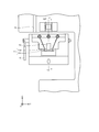
図4は、本実施形態に係る本体部10の上面を平面視した図である。図5は、図4のT1-T1’位置における本体部10の断面図である。図6は、図4のT2-T2’位置における本体部10の断面図である。
図7は、本実施形態に係る固定部14の構成を示す拡大図である。尚、図7では、説明の便宜として、端子ガイド溝11の側壁の図示を省略している。図8は、本実施形態に係る導電性接触子17の構成を示す図である。
本実施形態に係る試験装置1は、支持台100、本体部10、端子ガイド溝11、基板ガイド溝12、誘導部13、固定部14、接続中継基板15、可動ユニット16、導電性接触子17、操作部材18、及び、駆動手段19を備えている。
本体部10は、回路基板20の載置台である。本体部10は、自身の上面(回路基板20が載置される面を表す。以下同じ)に回路基板20が載置された際に、当該回路基板20の接続端子23を自身の内部に受け入れ、本体部10内に配設された接続中継基板15と電気接続させる。本体部10は、例えば、上面が地面に対して30度~70度程度傾斜するように、支持台100に取り付けられている。
基板ガイド溝12(本発明の「基板ガイド」に相当)は、本体部10において、回路基板20の外形に沿うように形成され、回路基板20を当該回路基板20の基板面の延在方向に沿って載置位置に案内する(図1を参照)。具体的には、基板ガイド溝12は、本体部10の上面に沿って上方から下方に延在し、回路基板20を上方から下方に移動させるようにして、載置位置に案内する。尚、基板ガイド溝12が規定する載置位置は、例えば、当該基板ガイド溝12の下端部であり、回路基板20は、基板ガイド溝12の下端部に到達した時点で移動が規制され、当該基板ガイド溝12内の載置位置に載置されることになる。
端子ガイド溝11は、基板ガイド溝12内において、回路基板20の接続端子23(又はフレキシブル基板22)の外形に沿うように形成され、回路基板20が基板ガイド溝12内を移動するときに、接続端子23を自身が規定する本体部10内の接続位置P(図5の点線領域Pを参照)に案内する。尚、端子ガイド溝11は、基板ガイド溝12内に配設され、当該基板ガイド溝12と略同一の方向(即ち、上方側から下方側)に向かって延在する。
端子ガイド溝11は、本体部10の上面側に露出した第1溝部11aと、当該第1溝部11aから本体部10内の接続位置Pに延在する第2溝部11bと、接続端子23が接続位置Pに到達したときに接続端子23の移動を規制するストッパ11cと、を有する。
第1溝部11aの延在方向(図5を参照)は、基板ガイド溝12の延在方向(溝の長手方向を意味する。以下同じ)に対して、本体部10の内部側に10度以上で且つ60度以下、より好適には、20度以上で且つ40度以下の傾斜角度(図5のθ1を参照)を有する。尚、本実施形態では、第1溝部11aは、接続端子23を第2溝部11bに案内しやすくする観点から、上方から下方に向かって段階的に傾斜角度を大きくした態様を示している。
第2溝部11bの延在方向は、第1溝部11aの延在方向に対して、更に本体部10の内部側に傾斜するのが望ましい。第2溝部11bの延在方向は、例えば、基板ガイド溝12の延在方向に対する傾斜角度(図5のθ2を参照)が、第1溝部11aの傾斜角度(図5のθ1を参照)よりも大きくなるように、本体部10の内部側に30度以上で且つ90度以下の傾斜角度を有する構成とする。但し、第2溝部11bの延在方向は、第1溝部11aの延在方向と同一直線状であってもよい。
ストッパ11cは、接続端子23が第2溝部11b内の接続位置Pに到達したときに、接続端子23の移動をストップさせる。ストッパ11cは、例えば、第2溝部11bの終端位置に形成された段付き部であって、接続位置Pに到達した接続端子23と当接して、接続端子23の移動を規制する。ストッパ11cにて移動が規制されることにより、接続端子23は、おおまかに接続位置Pに位置決めされることになる。
端子ガイド溝11は、かかる構成によって、回路基板20が基板ガイド溝12に沿って上方から下方に移動するときに、フレキシブル基板22及び接続端子23の移動方向を規制し、接続端子23を本体部10内の接続位置Pまで案内する。
誘導部13は、端子ガイド溝11の第1溝部11a内に配設され、接続端子23が基板ガイド溝12内を移動するときに、当該接続端子23を端子ガイド溝11側に誘導する(図4、図5を参照)。誘導部13は、例えば、端子ガイド溝11の第1溝部11a内に埋設されたマグネットである。ここでは、誘導部13(マグネット)は、第1溝部11aの底面から突出しないように第1溝部11a内に埋設され、第1溝部11aの中間位置から、第1溝部11aと第2溝部11bとの区切り位置まで延在する。そして、誘導部13は、接続端子23が、通常、鉄材(例えば、SUS)を含んでいることを利用して、磁力により接続端子23を端子ガイド溝11側に吸引する。接続端子23は、誘導部13にて接続端子23を吸引されることによって、回路基板20が上方から下方に移動するに伴って、第1溝部11aから第2溝部11bに円滑に移動する。
固定部14は、端子ガイド溝11の接続位置P上において、端子ガイド溝11に対して上下(即ち、近接方向又は離間方向)に移動可能に配設されている(図5を参照)。換言すると、固定部14は、接続位置P上において、端子ガイド溝11内に突出可能且つ端子ガイド溝11外に退避可能に配設されている。そして、固定部14は、例えば、接続端子23の外形に沿った窪み形状を呈し、端子ガイド溝11の第2溝部11bに対して下降したときに、接続位置Pに案内された接続端子23と嵌合することにより、接続端子23を位置決め固定する。
より詳細には、固定部14は、接続端子23を位置決め固定する際には、接続位置Pに案内された接続端子23を、端子ガイド溝11の上方から覆うように下降して、接続端子23の周囲の側面と当接する。これによって、接続端子23は、当該接続端子23の四方向の側面が固定部14とストッパ11cとによって囲繞されるように、固定部14に嵌合し、これによって位置決め固定される。
導電性接触子17は、接続端子23と接続中継基板15との間の信号路を形成する。導電性接触子17は、端子ガイド溝11の接続位置P上において、端子ガイド溝11に対して上下(即ち、近接方向又は離間方向)に移動可能に配設されている(図5を参照)。換言すると、導電性接触子17は、接続位置P上において、端子ガイド溝11内に突出可能且つ端子ガイド溝11外に退避可能に配設されている。そして、導電性接触子17は、端子ガイド溝11の第2溝部11bに対して下降したときに、接続位置Pに位置決め固定された接続端子23と先端同士で点接触する。又、導電性接触子17は、端子ガイド溝11に向き合う側と反対側の端部において、接続中継基板15に設けられたパッドと接触する。
導電性接触子17は、例えば、接続端子23が有する32本のピン型端子それぞれに対応する位置に設けられた32本のコンタクトピンである(図8を参照)。各導電性接触子17は、筒状のピンバレル17a、ピンバレル17aの上端部に上下方向に摺動可能な状態で連結された第1プランジャ17b、ピンバレル17aの下端部に上下方向に摺動可能な状態で連結された第2プランジャ17c、及び、ピンバレル17a内において第1プランジャ17bと第2プランジャ17cとの間に配設されたスプリング17dを含んで構成される。そして、導電性接触子17は、スプリング17dが第2プランジャ17cを上方向に付勢すると共に第1プランジャ17bを下方向に付勢することにより、第1プランジャ17bの上端部と接続端子23との接触圧力、及び、第2プランジャ17cの下端部と接続中継基板15のパッドとの接触圧力を確保する。
尚、各導電性接触子17は、第1プランジャ17bと第2プランジャ17cとが露出するように、可動ユニット16に形成された貫通孔内に配設されている。
接続中継基板15は、回路基板20に対して電気信号を送出して、当該回路基板20の電気的試験を実施する。接続中継基板15は、下面に半田ボールを有し、当該半田ボールにて、導電性接触子17の第1プランジャ17bと接触する。そして、接続中継基板15は、回路基板20の接続端子23が接続位置Pに案内されたときに、導電性接触子17を介して接続端子23と電気接続し、これにより、回路基板20の電気的試験を実施する。
可動ユニット16は、固定部14及び導電性接触子17が、端子ガイド溝11の接続位置Pにおいて、端子ガイド溝11に対して上下(即ち、近接方向又は離間方向)に移動し得るように、固定部14及び導電性接触子17を支持する。つまり、固定部14及び導電性接触子17は、可動ユニット16と共に一体的に移動する。
操作部材18は、例えば、操作者が操作を行う回転レバーである。操作部材18は、例えば、本体部10の外側で駆動手段19のカムシャフト19bに取り付けられ、操作者の操作に応じて、カムシャフト19bに対してスプリング19dの付勢力に抗する駆動力を付与する。
駆動手段19は、可動ユニット16を上下(即ち、近接方向又は離間方向)に移動させ、接続端子23及び導電性接触子17を、端子ガイド溝11側に近づけ、又、端子ガイド溝11側から退避させる。
駆動手段19は、カムシャフト19b、カム受け部材19c、スプリング19d、及び、ボルト19eを有している。
ここで、スプリング19dは、可動ユニット16に端子ガイド溝11から離れる方向に付勢力を与える。カムシャフト19bは、本体部10に回転自在に軸支され、操作部材18(回転レバー)の回転操作に応じて回転し、カム受け部材19cを下降させ、当該カム受け部材19cを介して、スプリング19dの付勢力に抗して、可動ユニット16を端子ガイド溝11側に向けて下降させる。
ボルト19eは、接続中継基板15、可動ユニット16、及び、カム受け部材19cを一体的に固定する。これにより、接続中継基板15、可動ユニット16、及び、カム受け部材19cは、駆動手段19の動作によって、一体的に上下することになる。
[試験装置に対する回路基板の取り付け方法]
次に、図1、図9A、図9B、図9Cを参照して、試験装置1に対する回路基板20の取り付け方法について説明する。
次に、図1、図9A、図9B、図9Cを参照して、試験装置1に対する回路基板20の取り付け方法について説明する。
図9A、図9B、図9Cは、本実施形態に係る試験装置1に対する回路基板20の取り付け方法を説明する図である。図9A、図9B、図9Cは、試験装置1に対して回路基板20を取り付ける際の各部の状態を時系列に示している。
尚、本実施形態では、操作者の手作業により、回路基板20を移動させるものとするが、自動搬送装置によって回路基板20を移動させる態様としてもよい。
試験装置1に対して、回路基板20を取り付ける際には、操作者は、まず、回路基板20の下面が本体部10の上面と平行になるように、回路基板20を本体部10の鉛直方向上方側に配する(図1を参照)。尚、この際には、固定部14及び導電性接触子17は、端子ガイド溝11から離間した状態とされる。
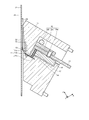
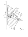
次に、操作者は、回路基板20を、本体部10の上面の基板ガイド溝12に沿って本体部10の上方から下方に向けて移動させる(図9Aを参照)。このとき、回路基板20は、本体部10の上面に形成された基板ガイド溝12に案内されて、本体部10の上方から下方に向けて移動する。そうすると、回路基板20の接続端子23は、誘導部13によって、本体部10の上面に形成された端子ガイド溝11の第1溝部11aに引き寄せられるようにして、当該第1溝部11aから第2溝部11b(即ち、本体部10の内部)に向けて移動する(図9Aの矢印を参照)。
更に、操作者は、回路基板20を、本体部10の上面の基板ガイド溝12に沿って本体部10の上方から下方に向けて移動させる(図9Bを参照)。そうすると、回路基板20の接続端子23は、端子ガイド溝11の第2溝部11bを本体部10の内部側に向けて移動する。そして、接続端子23は、端子ガイド溝11の接続位置Pまで到達した際に、ストッパ11cに当接して、移動が規制される(図9Bの矢印を参照)ため、当該接続端子23は、端子ガイド溝11の接続位置Pに位置決めされることになる。尚、このとき、回路基板20は、基板ガイド溝12の下端に到達した時点で移動が規制され、当該基板ガイド溝12内に載置される。
次に、操作者は、回路基板20を基板ガイド溝12内に載置した状態で、操作部材18を操作して、可動ユニット16を下方側に向けて移動させる(図9Cを参照)。これにより、可動ユニット16に支持された固定部14及び導電性接触子17は、下方側に向けて移動する(図9Cの矢印を参照)。このとき、固定部14は、回路基板20の接続端子23と嵌合するように、当該接続端子23を接続位置Pに位置決め固定する。又、このとき、導電性接触子17は、接続位置Pに位置決め固定された回路基板20の接続端子23と接触し、回路基板20の接続端子23との間で電気接続する。尚、このとき、導電性接触子17の32本のコンタクトピン17それぞれが、回路基板20の32本のピン型端子それぞれと、先端同士を突き合わせるようにして、接触することになる。
このようにして、導電性接触子17と回路基板20の接続端子23とが電気接続することによって、接続中継基板15は、導電性接触子17を介して、回路基板20の接続端子23と電気接続する。そして、接続中継基板15は、導電性接触子17及び回路基板20の接続端子23を介して、回路基板20の電子部品24に対して電気信号(即ち、試験信号)を送信し、回路基板20に対する試験を実施する。
[効果]
以上のように、本実施形態に係る試験装置1によれば、回路基板20を基板ガイド溝12に沿って移動させるだけで、当該接続端子23を接続位置Pに案内することができ、加えて、その後、固定部14及び導電性接触子17を下降させる操作のみで、当該接続端子23と導電性接触子17とを確実に電気的に接続することができる。これによって、容易に、回路基板20の電気的試験を実施することができる。
以上のように、本実施形態に係る試験装置1によれば、回路基板20を基板ガイド溝12に沿って移動させるだけで、当該接続端子23を接続位置Pに案内することができ、加えて、その後、固定部14及び導電性接触子17を下降させる操作のみで、当該接続端子23と導電性接触子17とを確実に電気的に接続することができる。これによって、容易に、回路基板20の電気的試験を実施することができる。
特に、本実施形態に係る試験装置1は、回路基板20の陰になって、接続端子23の位置が視認できない状態であっても、容易に、回路基板20に設けられた接続端子23と導電性接触子17とを電気的に接続することができる点で、有用である。
(第2の実施形態)
次に、図10~図11を参照して、第2の実施形態に係る試験装置1の構成について説明する。本実施形態に係る試験装置1は、フレキシブル基板22の移動経路を規制するガイドローラ10Tを有する点で、第1の実施形態と相違する。尚、第1の実施形態と共通する構成については、説明を省略する。
次に、図10~図11を参照して、第2の実施形態に係る試験装置1の構成について説明する。本実施形態に係る試験装置1は、フレキシブル基板22の移動経路を規制するガイドローラ10Tを有する点で、第1の実施形態と相違する。尚、第1の実施形態と共通する構成については、説明を省略する。
図10は、本実施形態に係る本体部10の上面を平面視した図である。図11は、図10のT3-T3’位置における本体部10の断面図である。
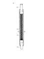
本実施形態に係る試験装置1は、特に、フレキシブル基板22の配線長が長い場合に生じる問題を解消する。具体的には、フレキシブル基板22の配線長が長い場合には、当該フレキシブル基板22は、長手方向に沿って湾曲状に弾性変形しやすい状態となる。そのため、回路基板20を基板ガイド溝12に沿って案内して、接続端子23が端子ガイド溝11の第2溝部11b内に入り込む位置に到達して、第2溝部11bの入り口付近の溝壁部に衝突した際に、当該フレキシブル基板22は、湾曲状に弾性変形してしまうおそれがある。その結果、接続端子23が端子ガイド溝11(第2溝部11b)内に入り込まない場合がある。
ガイドローラ10Tは、上記事態を抑制するべく設けられており、回路基板20が基板ガイド溝12によって案内されるときに、接続端子23が端子ガイド溝11内に案内されるように、フレキシブル基板22の移動経路を規制する。
ガイドローラ10Tは、例えば、基板ガイド溝12の溝底面から露出した状態で、基板ガイド溝12内に埋設されている。又、ガイドローラ10Tは、自身の下端に配設されたスプリング10Taを介して、本体部10内に固定されている。そして、ガイドローラ10Tは、スプリング10Taの上下動により、基板ガイド溝12内において、当該基板ガイド溝12の底面から外側に突出可能に、且つ、当該基板ガイド溝12の底面と略面一まで退避可能に配設されている。
又、ガイドローラ10Tは、回路基板20が基板ガイド溝12によって案内される方向に沿って回転可能に軸支されている。
かかる構成により、回路基板20が基板ガイド溝12によって案内されるとき、ガイドローラ10Tは、フレキシブル基板22の下面と当接し、スプリング10Taの反発力によって、フレキシブル基板22の一部を回路基板20の下面に押し付ける。そして、ガイドローラ10Tは、回路基板20が基板ガイド溝12に沿って下方側に移動するに伴って、回転しながらフレキシブル基板22を下方側に案内する。
これにより、フレキシブル基板22は、回路基板20が基板ガイド溝12によって案内されるとき、フレキシブル基板22がガイドローラ10Tにて回路基板20の下面に押し付けられた位置を起点として移動することになる。つまり、これにより、接続端子23が第2溝部11bの入り口付近の溝壁部に衝突したときに、フレキシブル基板22に作用する曲げモーメントは、フレキシブル基板22がガイドローラ10Tにて回路基板20の下面に押し付けられた位置を起点として生ずることになる。従って、本実施形態においてフレキシブル基板22に作用する曲げモーメントは、ガイドローラ10Tが設けられない場合と比較して小さくなる。
これによって、フレキシブル基板22が湾曲状に変形することを抑制することができる。又、このように、フレキシブル基板22の変形が抑制されることによって、フレキシブル基板22の先端部が端子ガイド溝11から横方向にずれることも抑制できる。
以上のように、本実施形態に係る試験装置1によれば、より円滑に、接続端子23を端子ガイド溝11内に案内することが可能である。
(その他の実施形態)
本発明は、上記実施形態に限らず、種々に変形態様が考えられる。
本発明は、上記実施形態に限らず、種々に変形態様が考えられる。
例えば、上記実施形態では、操作者の手作業により、回路基板20を試験装置1に載置させたり、操作部材18を操作したりする態様を示した。しかしながら、これらは、自動搬送装置等によって実施される構成としてもよい。
又、上記実施形態では、誘導部13の一例として、マグネットを示した。しかしながら、誘導部13としては、マグネットに代えて、吸気によって、回路基板20の接続端子23を端子ガイド溝11側に吸引する吸気孔等が用いられてもよい。
又、上記実施形態では、第1溝部11aに誘導部13を有する態様を示したが、第2溝部11b側から回路基板20へ向けて送気することで、接続端子23を第1溝部11aに引き寄せるための送気孔が第2溝部11bに設けられていてもよい。
又、上記実施形態では、基板ガイド溝12の一例として、本体部10の上面に露出した溝形状の態様を示した。しかしながら、基板ガイド溝12は、一端に回路基板20を挿入可能な開口を有していれば、本体部10の内部に設けられてもよい。
又、上記実施形態では、回路基板20を載置位置に案内する構成を、基板ガイド溝12によって行う態様を示した。しかしながら、本発明の試験装置1は、基板ガイド溝12に代えて、ガイドローラ等を用いて、回路基板20を、回路基板20の基板面の延在方向に沿って載置位置に案内する態様とされてもよい。
又、上記実施形態では、試験対象の回路基板20として、ディスプレイパネルを用いる態様を示した。しかしながら、試験対象の回路基板20としては、ICチップ等が用いられてもよい。
以上、本発明の具体例を詳細に説明したが、これらは例示にすぎず、請求の範囲を限定するものではない。請求の範囲に記載の技術には、以上に例示した具体例を様々に変形、変更したものが含まれる。
本出願は、2018年11月12日出願の特願2018-212011及び2018年12月10日出願の特願2018-230913に基づく優先権を主張する。これらの出願明細書および図面に記載された内容は、すべて本願明細書に援用される。
本開示に係る試験装置によれば、簡易に、回路基板の電気的試験を行うことが可能となる。
1 試験装置
10 本体部
10T ガイドローラ
10Ta スプリング
11 端子ガイド溝
11a 第1溝部
11b 第2溝部
11c ストッパ
12 基板ガイド溝
13 誘導部
14 固定部
15 接続中継基板
16 可動ユニット
17 導電性接触子
17a ピンバレル
17b 第1プランジャ
17c 第2プランジャ
17d スプリング
18 操作部材
19 駆動手段
19b カムシャフト
19c カム受け部材
19d スプリング
19e ボルト
100 支持台
P 接続位置
20 回路基板
21 基板部
22 フレキシブル基板
23 接続端子
24 電子部品
10 本体部
10T ガイドローラ
10Ta スプリング
11 端子ガイド溝
11a 第1溝部
11b 第2溝部
11c ストッパ
12 基板ガイド溝
13 誘導部
14 固定部
15 接続中継基板
16 可動ユニット
17 導電性接触子
17a ピンバレル
17b 第1プランジャ
17c 第2プランジャ
17d スプリング
18 操作部材
19 駆動手段
19b カムシャフト
19c カム受け部材
19d スプリング
19e ボルト
100 支持台
P 接続位置
20 回路基板
21 基板部
22 フレキシブル基板
23 接続端子
24 電子部品
Claims (10)
- 一方側の面から引き出されたフレキシブル基板、及び、前記フレキシブル基板の端部に配された接続端子を有する回路基板に対して、電気的試験を実施する試験装置であって、
前記回路基板を、前記回路基板の基板面の延在方向に沿って載置位置に案内する基板ガイド、及び、前記回路基板が前記基板ガイドによって案内されるときに、前記接続端子を所定位置に案内する端子ガイド溝を有する本体部と、
前記接続端子が前記基板ガイドによって案内されるときに、前記接続端子を前記端子ガイド溝側に誘導する誘導部と、
前記所定位置において、前記端子ガイド溝内に突出可能且つ前記端子ガイド溝外に退避可能に配設され、前記端子ガイド溝内に突出した際に、前記所定位置に案内された前記接続端子を位置決め固定する固定部と、
前記所定位置において、前記端子ガイド溝内に突出可能且つ前記端子ガイド溝外に退避可能に配設され、前記端子ガイド溝内に突出した際に、前記所定位置に案内された前記接続端子と電気接続する導電性接触子と、
を備える試験装置。 - 前記誘導部は、マグネットである、
請求項1に記載の試験装置。 - 前記端子ガイド溝の延在方向は、前記基板ガイドの延在方向に対して、10度以上で且つ60度以下の傾斜角度を有する、
請求項1又は2に記載の試験装置。 - 前記端子ガイド溝は、前記本体部の上面側に露出した第1溝部と、前記第1溝部から前記所定位置まで延在する第2溝部と、前記接続端子が前記所定位置に到達したときに前記接続端子の移動を規制するストッパと、を有する、
請求項1乃至3のいずれか一項に記載の試験装置。 - 前記接続端子は、複数本のピン型接続端子を含んで構成され、
前記導電性接触子は、前記接続端子の複数本のピン型接続端子それぞれに対応する複数のコンタクトピンを含んで構成される、
請求項1乃至4のいずれか一項に記載の試験装置。 - 前記回路基板は、ディスプレイパネルである、
請求項1乃至5のいずれか一項に記載の試験装置。 - 前記固定部及び前記導電性接触子は、前記所定位置において、駆動手段により、前記端子ガイド溝に対して上下に移動する可動ユニットに支持されている、
請求項1乃至6のいずれか一項に記載の試験装置。 - 前記駆動手段は、
前記可動ユニットに対して、前記端子ガイド溝から離れる方向に付勢力を与える弾性部材と、
前記本体部に回転自在に軸支され、前記弾性部材の付勢力に抗する駆動力が付与された際に、前記可動ユニットを前記端子ガイド溝側に向けて近接させるカムシャフトと、
前記本体部の外側で前記カムシャフトに取り付けられ、外部からの外力により、前記カムシャフトに対して前記駆動力を付与する操作部材と、を有する、
請求項7に記載の試験装置。 - 前記回路基板が前記基板ガイドによって案内されるときに、前記接続端子が前記端子ガイド溝内に案内されるように、前記フレキシブル基板の移動経路を規制するガイドローラを有する、
請求項1乃至8のいずれか一項に記載の試験装置。 - 前記ガイドローラは、前記フレキシブル基板の一部を前記回路基板の下面に押し付けるようにして、前記フレキシブル基板の移動経路を規制する、
請求項9に記載の試験装置。
Applications Claiming Priority (4)
| Application Number | Priority Date | Filing Date | Title |
|---|---|---|---|
| JP2018212011 | 2018-11-12 | ||
| JP2018-212011 | 2018-11-12 | ||
| JP2018-230913 | 2018-12-10 | ||
| JP2018230913A JP2020079779A (ja) | 2018-11-12 | 2018-12-10 | 試験装置 |
Publications (1)
| Publication Number | Publication Date |
|---|---|
| WO2020100850A1 true WO2020100850A1 (ja) | 2020-05-22 |
Family
ID=70731222
Family Applications (1)
| Application Number | Title | Priority Date | Filing Date |
|---|---|---|---|
| PCT/JP2019/044231 Ceased WO2020100850A1 (ja) | 2018-11-12 | 2019-11-12 | 試験装置 |
Country Status (1)
| Country | Link |
|---|---|
| WO (1) | WO2020100850A1 (ja) |
Citations (6)
| Publication number | Priority date | Publication date | Assignee | Title |
|---|---|---|---|---|
| JPS5842672U (ja) * | 1981-09-14 | 1983-03-22 | 富士通株式会社 | プリント板試験用接続具の構造 |
| JP2557067Y2 (ja) * | 1992-06-05 | 1997-12-08 | 株式会社ヨコオ | クリップ式中継コネクタ |
| JPH1186993A (ja) * | 1997-09-12 | 1999-03-30 | Fujitsu Denso Ltd | プリント配線板用試験接続器 |
| JP2005025965A (ja) * | 2003-06-30 | 2005-01-27 | Enplas Corp | 電気部品用ソケット |
| JP2008135209A (ja) * | 2006-11-27 | 2008-06-12 | Fujifilm Corp | クリップ式コネクタ |
| JP2010015894A (ja) * | 2008-07-04 | 2010-01-21 | Asuka Denki Seisakusho:Kk | 検査用コネクター |
-
2019
- 2019-11-12 WO PCT/JP2019/044231 patent/WO2020100850A1/ja not_active Ceased
Patent Citations (6)
| Publication number | Priority date | Publication date | Assignee | Title |
|---|---|---|---|---|
| JPS5842672U (ja) * | 1981-09-14 | 1983-03-22 | 富士通株式会社 | プリント板試験用接続具の構造 |
| JP2557067Y2 (ja) * | 1992-06-05 | 1997-12-08 | 株式会社ヨコオ | クリップ式中継コネクタ |
| JPH1186993A (ja) * | 1997-09-12 | 1999-03-30 | Fujitsu Denso Ltd | プリント配線板用試験接続器 |
| JP2005025965A (ja) * | 2003-06-30 | 2005-01-27 | Enplas Corp | 電気部品用ソケット |
| JP2008135209A (ja) * | 2006-11-27 | 2008-06-12 | Fujifilm Corp | クリップ式コネクタ |
| JP2010015894A (ja) * | 2008-07-04 | 2010-01-21 | Asuka Denki Seisakusho:Kk | 検査用コネクター |
Similar Documents
| Publication | Publication Date | Title |
|---|---|---|
| US4841241A (en) | Testing device for both-sided contacting of component-equipped printed circuit boards | |
| US5754057A (en) | Contact mechanism for test head of semiconductor test system | |
| US8438722B2 (en) | Apparatus and method for detecting component attachment | |
| JP2000074994A (ja) | テストソケット | |
| CN108663546A (zh) | 测试插座 | |
| KR101574486B1 (ko) | 테스트 소켓 | |
| KR20190027923A (ko) | 전기적 접속 장치 | |
| CN101162298A (zh) | 面板检查装置及方法 | |
| JP6027778B2 (ja) | 部品取付装置、部品取付方法 | |
| KR101246105B1 (ko) | 반도체 패키지 테스트용 소켓 | |
| TWI429148B (zh) | A substrate mounting device, a test head, and an electronic component testing device | |
| JP2019021554A (ja) | 電子機器組立装置及び電子機器組立方法 | |
| KR100774914B1 (ko) | 평판 디스플레이 모듈의 테스트용 지그 | |
| KR100586786B1 (ko) | 전기 부품용 소켓 | |
| WO2020100850A1 (ja) | 試験装置 | |
| KR102037446B1 (ko) | 하부접속방식의 평판 디스플레이 패널용 검사장치 | |
| KR101466739B1 (ko) | 인쇄회로기판 검사장치 | |
| KR100751508B1 (ko) | 인쇄회로기판 검사장치 | |
| JP2020079779A (ja) | 試験装置 | |
| KR20210101357A (ko) | 볼 배치 시스템 및 기판 상에 볼을 배치하는 방법 | |
| KR100488891B1 (ko) | 전기부품용 소켓 및 그 조립방법 | |
| US8113084B2 (en) | Mounting device | |
| CN108200262A (zh) | 一种手机天线测试装置 | |
| KR100610778B1 (ko) | 반도체 소자 테스트 핸들러용 캐리어 모듈 | |
| CN112363088B (zh) | 一种定位结构及测试装置 |
Legal Events
| Date | Code | Title | Description |
|---|---|---|---|
| 121 | Ep: the epo has been informed by wipo that ep was designated in this application |
Ref document number: 19884581 Country of ref document: EP Kind code of ref document: A1 |
|
| NENP | Non-entry into the national phase |
Ref country code: DE |
|
| 122 | Ep: pct application non-entry in european phase |
Ref document number: 19884581 Country of ref document: EP Kind code of ref document: A1 |