WO2020100614A1 - はんだ接合部及びその製造方法 - Google Patents
はんだ接合部及びその製造方法 Download PDFInfo
- Publication number
- WO2020100614A1 WO2020100614A1 PCT/JP2019/042814 JP2019042814W WO2020100614A1 WO 2020100614 A1 WO2020100614 A1 WO 2020100614A1 JP 2019042814 W JP2019042814 W JP 2019042814W WO 2020100614 A1 WO2020100614 A1 WO 2020100614A1
- Authority
- WO
- WIPO (PCT)
- Prior art keywords
- solder
- metal base
- base material
- substrate
- weight
- Prior art date
- Legal status (The legal status is an assumption and is not a legal conclusion. Google has not performed a legal analysis and makes no representation as to the accuracy of the status listed.)
- Ceased
Links
Images






Classifications
-
- B—PERFORMING OPERATIONS; TRANSPORTING
- B23—MACHINE TOOLS; METAL-WORKING NOT OTHERWISE PROVIDED FOR
- B23K—SOLDERING OR UNSOLDERING; WELDING; CLADDING OR PLATING BY SOLDERING OR WELDING; CUTTING BY APPLYING HEAT LOCALLY, e.g. FLAME CUTTING; WORKING BY LASER BEAM
- B23K1/00—Soldering, e.g. brazing, or unsoldering
- B23K1/0008—Soldering, e.g. brazing, or unsoldering specially adapted for particular articles or work
- B23K1/0016—Soldering of electronic components
-
- B—PERFORMING OPERATIONS; TRANSPORTING
- B23—MACHINE TOOLS; METAL-WORKING NOT OTHERWISE PROVIDED FOR
- B23K—SOLDERING OR UNSOLDERING; WELDING; CLADDING OR PLATING BY SOLDERING OR WELDING; CUTTING BY APPLYING HEAT LOCALLY, e.g. FLAME CUTTING; WORKING BY LASER BEAM
- B23K1/00—Soldering, e.g. brazing, or unsoldering
- B23K1/19—Soldering, e.g. brazing, or unsoldering taking account of the properties of the materials to be soldered
-
- B—PERFORMING OPERATIONS; TRANSPORTING
- B23—MACHINE TOOLS; METAL-WORKING NOT OTHERWISE PROVIDED FOR
- B23K—SOLDERING OR UNSOLDERING; WELDING; CLADDING OR PLATING BY SOLDERING OR WELDING; CUTTING BY APPLYING HEAT LOCALLY, e.g. FLAME CUTTING; WORKING BY LASER BEAM
- B23K1/00—Soldering, e.g. brazing, or unsoldering
- B23K1/20—Preliminary treatment of work or areas to be soldered, e.g. in respect of a galvanic coating
-
- B—PERFORMING OPERATIONS; TRANSPORTING
- B23—MACHINE TOOLS; METAL-WORKING NOT OTHERWISE PROVIDED FOR
- B23K—SOLDERING OR UNSOLDERING; WELDING; CLADDING OR PLATING BY SOLDERING OR WELDING; CUTTING BY APPLYING HEAT LOCALLY, e.g. FLAME CUTTING; WORKING BY LASER BEAM
- B23K35/00—Rods, electrodes, materials, or media, for use in soldering, welding, or cutting
- B23K35/22—Rods, electrodes, materials, or media, for use in soldering, welding, or cutting characterised by the composition or nature of the material
- B23K35/24—Selection of soldering or welding materials proper
- B23K35/26—Selection of soldering or welding materials proper with the principal constituent melting at less than 400°C
-
- C—CHEMISTRY; METALLURGY
- C22—METALLURGY; FERROUS OR NON-FERROUS ALLOYS; TREATMENT OF ALLOYS OR NON-FERROUS METALS
- C22C—ALLOYS
- C22C28/00—Alloys based on a metal not provided for in groups C22C5/00 - C22C27/00
-
- C—CHEMISTRY; METALLURGY
- C22—METALLURGY; FERROUS OR NON-FERROUS ALLOYS; TREATMENT OF ALLOYS OR NON-FERROUS METALS
- C22C—ALLOYS
- C22C9/00—Alloys based on copper
- C22C9/06—Alloys based on copper with nickel or cobalt as the next major constituent
-
- B—PERFORMING OPERATIONS; TRANSPORTING
- B23—MACHINE TOOLS; METAL-WORKING NOT OTHERWISE PROVIDED FOR
- B23K—SOLDERING OR UNSOLDERING; WELDING; CLADDING OR PLATING BY SOLDERING OR WELDING; CUTTING BY APPLYING HEAT LOCALLY, e.g. FLAME CUTTING; WORKING BY LASER BEAM
- B23K2101/00—Articles made by soldering, welding or cutting
- B23K2101/36—Electric or electronic devices
- B23K2101/42—Printed circuits
-
- B—PERFORMING OPERATIONS; TRANSPORTING
- B23—MACHINE TOOLS; METAL-WORKING NOT OTHERWISE PROVIDED FOR
- B23K—SOLDERING OR UNSOLDERING; WELDING; CLADDING OR PLATING BY SOLDERING OR WELDING; CUTTING BY APPLYING HEAT LOCALLY, e.g. FLAME CUTTING; WORKING BY LASER BEAM
- B23K2103/00—Materials to be soldered, welded or cut
- B23K2103/08—Non-ferrous metals or alloys
- B23K2103/12—Copper or alloys thereof
-
- B—PERFORMING OPERATIONS; TRANSPORTING
- B23—MACHINE TOOLS; METAL-WORKING NOT OTHERWISE PROVIDED FOR
- B23K—SOLDERING OR UNSOLDERING; WELDING; CLADDING OR PLATING BY SOLDERING OR WELDING; CUTTING BY APPLYING HEAT LOCALLY, e.g. FLAME CUTTING; WORKING BY LASER BEAM
- B23K2103/00—Materials to be soldered, welded or cut
- B23K2103/18—Dissimilar materials
- B23K2103/26—Alloys of Nickel and Cobalt and Chromium
Definitions
- the present invention relates to a solder joint and a method for manufacturing the same. More specifically, the present invention relates to a solder joint that enables soldering at a low temperature and a method for manufacturing the same.
- Low-temperature solders are drawing attention because they can be processed at low temperatures and can use substrates made of materials with low heat resistance.
- the low-temperature solder for example, In is 50 to 83 atomic% (35.4 to 72.8 mass%), the low temperature solder having a composition of the remaining Bi (Patent Document 1), In is 48 to 52.5 mass%, the balance Bi A lead-free low-temperature solder, which has a solidus temperature of 85 ° C. or higher and a liquidus temperature of 110 ° C. or lower, and the intermetallic compound of BiIn 2 is present in the structure of the lead-free low-temperature solder.
- lead-free low-temperature solders for joining electronic components, etc. Patent Document 2.
- liquidus temperature of the low-temperature solder is around 100 ° C., that is, 90 to 110 ° C.
- the flexibility is required so that the joint portion does not break even when the substrate is deformed, and further technical development has been required.
- An object of the present invention is to manufacture a solder joint part capable of joining metal members on a substrate even at 90 ° C. or lower, and having flexibility such that a deformable substrate such as a flexible substrate is hard to break. It is to provide a solder joint obtained by a manufacturing method.
- the inventors of the present invention have been studying a technique capable of joining an electronic circuit on a flexible substrate, and have adopted copper or a copper-nickel alloy as a metal base material provided on the substrate, In addition, it was found that the use of a gallium alloy as the bonding material enables bonding at a low temperature of 90 ° C. or less, and that the intermetallic compound generated between the metal members has flexibility, and the present invention was completed.
- the gist of the present invention is (1) A method for manufacturing a solder joint part in which a first metal base material and a second metal base material are bonded by soldering, At least one of the first metal base material and the second metal base material is an alloy having a Ni content of 0% by weight or more and less than 44% by weight and a Cu content of more than 56% by weight,
- the solder is a solder alloy consisting of Ga and unavoidable impurities or a solder alloy containing Ga as a main component and having a melting point of 30 ° C. or lower,
- a step of applying solder to the surface of the first metal base material, and then placing a second metal base material on the applied solder By heating to a temperature of 90 ° C.
- a method for manufacturing a solder joint including a step of joining a second metal material, (2) The method including the step of applying solder to the surface of the second metal base material and bringing the solder-applied surface of the first metal base material and the solder-applied surface of the second metal base material into contact with each other face to face.
- a method for manufacturing a solder joint part according to (3) The method for manufacturing a solder joint according to (1) or (2), wherein the solder is directly placed on the surface of the first or second metal base material.
- the first and second metal base materials are Cu—Ni alloys having a Ni content of more than 0% by weight, less than 44% by weight and a Cu content of more than 56% by weight.
- a method for manufacturing a solder joint according to any one of (5) The method for manufacturing a solder joint according to any one of (1) to (4) above, wherein the rare gas is argon gas or nitrogen gas.
- (6) The method for manufacturing a solder joint according to any one of (1) to (4), wherein the liquid is warm water or an aqueous solution of an inorganic acid.
- One of the (1) to (6), wherein one of the first and second metal base materials is a wiring formed on the electronic circuit board and the other is a terminal of an electronic component.
- a method for manufacturing a solder joint part according to (8) A solder joint part in which the first metal base material and the second metal base material are bonded via a solder layer, At least one of the first metal base material and the second metal base material is an alloy having a Ni content of 0% by weight or more and less than 44% by weight and a Cu content of more than 56% by weight, A solder joint in which the solder layer is composed of a continuous phase of an intermetallic compound of Cu, Ni and Ga and contains CuGa2 or (Cu, Ni) Ga2; Regarding
- solder joining method of the present invention joining can be performed even at a heating temperature of 90 ° C or lower. Therefore, in addition to reducing the load on the base material due to the temperature at the time of joining, it becomes possible to manufacture an electronic circuit using a substrate made of a resin, which has been difficult to carry out in the past.
- electronic components having low heat resistance such as LEDs and pressure sensors, and liquid solder are used in the present invention, for example, dispensers, jet printers, and the like are used and applied to fine parts and 3D. Is possible.
- the solder joint portion of the present invention has flexibility that does not easily break even when deformed, it can be suitably used in the field of microelectronics such as electronic circuits in flexible substrates.
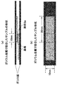
- FIG. 1 shows a schematic view of a solder joint part manufactured in Example 1.
- FIG. 1 (a) is a cross-sectional view from the lateral direction
- FIG. 1 (b) is a schematic view from the above.
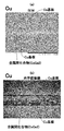
- Sectional drawing with the SEM (scanning electron microscope) (FIG. 2A) and the optical microscope (FIG. 2B) of the solder joint part in a Cu substrate is shown.
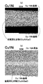
- FIG. 3 shows a cross-sectional view of a solder joint portion of a Cu-1% Ni substrate with an SEM (FIGS. 3 (a) and 3 (b)).
- FIG. 4 is a cross-sectional view of a solder joint portion of a Cu-10% Ni substrate with an SEM (FIG. 4A) and an optical microscope (FIG. 4B).
- FIG. 5A shows an SEM image of the Ga—Cu IMC (intermetallic compound) layer on the Cu substrate in Test Example 1.
- FIGS. 5B and 5C show the results of energy dispersive X-ray spectroscopy (EDS) elemental mapping of the cross section of the Ga—Cu IMC / Cu bond interface.
- FIG. 6 shows the indexed results of the synchrotron XRD pattern of Ga—Cu IMC powder in Test Example 2.
- FIG. 7A shows the average coefficient of thermal expansion (CTE) at 100 ° C. in Test Example 3.
- FIG. 7 (b) shows the maximum CTE mismatch, and
- FIG. 7 (c) shows the CTE anisotropy of CuGa 2, ⁇ Sn and the main solder IMC at 100 ° C.
- FIG. 8 is an SEM image (a) showing the position of the sample on which the nanoindentation measurement was performed and EBSD (Electron Back Scatter Diffraction Patterns) Kikuchi patterns (b) and (c) of CuGa2 at the indentation measurement position of each name. Indicates.
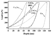
- FIG. 9 shows the result of the nanoindentation load-displacement curve of Ga-Cu IMC in Test Example 4.
- 10A and 10B show hardness (a) and Young's modulus (b) of CuGa2, Cu, Sn, and main solder IMC in Test Example 4.
- the data of Cu, ⁇ Sn, and main solder IMC are publicly known.
- FIG. 8 is an SEM image (a) showing the position of the sample on which the nanoindentation measurement was performed and EBSD (Electron Back Scatter Diffraction Patterns) Kikuchi patterns (b) and (c) of CuGa2 at the indentation measurement position of each name. Indicates.
- FIG. 9 shows the result
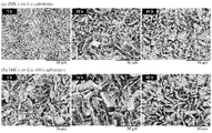
- FIG. 11 shows a top-view backscattered electron (BSE) image of IMC on a metal substrate after being contacted with Ga at 30 ° C. for 5 to 40 hours in Test Example 6, and FIG. 11 (b) shows the results with the Cu-10Ni substrate.
- FIG. 12 shows a backscattered electron (BSE) image of a cross-section sample in Test Example 6, where FIG. 12 (a) shows the IMC on the Cu substrate after contact with Ga at 30 ° C. for 5 to 40 hours and FIG. ) Indicates IMC on Cu-10Ni substrate.
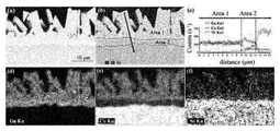
- FIG. 13 (a) shows an SEM backscattering image of IMC on a Cu-10Ni substrate, and FIGS.
- FIG. 14A shows a SEM image of the Ga / Cu interface at a reaction time of 70 hours in Test Example 6, and the rectangle in the figure shows the TEM observation region of FIG. 14B.
- FIG. 14C shows an SEM image of the Ga / Cu interface at a reaction time of 142 hours, and the rectangle in the figure shows the TEM observation region of FIG. 14D.
- FIG. 15 shows a synchrotron transmission XRD pattern of Ga / substrate IMC on a Cu substrate (bottom) and a Cu-10Ni substrate (top) in Test Example 6 at 25 ° C.
- FIG. 14A shows a SEM image of the Ga / Cu interface at a reaction time of 70 hours in Test Example 6, and the rectangle in the figure shows the TEM observation region of FIG. 14B.
- FIG. 14C shows an SEM image of the Ga / Cu interface at a reaction time of 142 hours, and the rectangle in the figure shows the TEM observation region of FIG. 14D.
- FIG. 15 shows a synchrotron transmission X
- FIG. 16A shows a backscattering SEM image of the IMC / Cu-10Ni couple sample in Test Example 6.
- the FIB sample was obtained from the interface region.
- FIG. 16 (b) shows a transmitted bright field at low magnification of the FIB device, and red circles show selected regions of the diffraction pattern.
- FIGS. 16 (c) and 16 (d) show high-resolution HAADF images of area 1 having FFT patterns on the zone axes [100] and [001] after tilting, respectively.
- FIG. 16E shows a high resolution HAADF image of area 2.
- FIG. 16F shows SADP in area 2 and its strength.
- FIG. 17 is a graph showing the results of the 25 ° C.
- FIG. 18 (a), 18 (b) and 18 (c) show the lattice constants of CuGa2 obtained at 25 ° C. to 200 ° C. in Test Example 6.
- 18 (a) shows the a-axis
- FIG. 18 (b) shows the c-axis
- FIG. 18 (c) shows the unit cell volume.
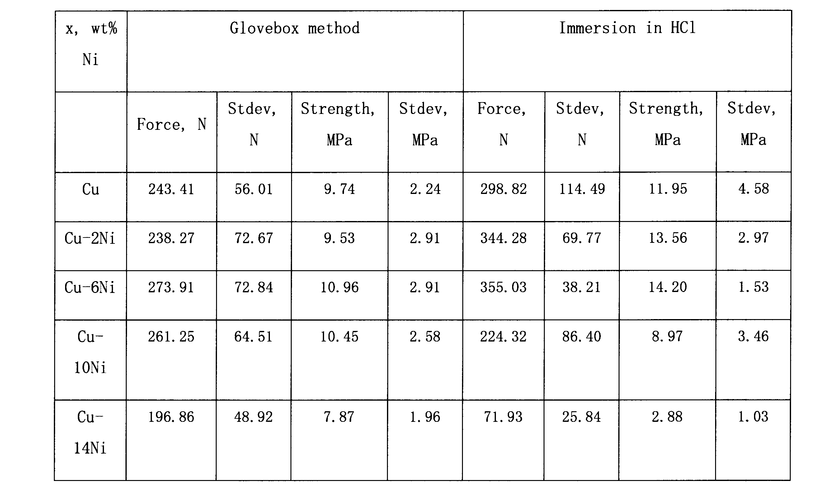
- FIG. 19 is a graph showing the results of the shear strength of the samples of the solder joints obtained in Examples 2 and 3 in Test Example 7.
- the method for manufacturing a solder joint of the present invention is A method for manufacturing a solder joint, in which a first metal base material and a second metal base material are bonded by soldering, At least one of the first metal substrate and the second metal substrate is an alloy having a Ni content of 0% by weight or more and less than 44% by weight and a Cu content of more than 56% by weight.
- the solder is a solder alloy composed of Ga and unavoidable impurities or a solder alloy containing Ga as a main component and having a melting point of 30 ° C.
- the first metal base material and the second metal base material are both base materials that form an electronic circuit, and the two are electrically connected by being joined by solder.
- one of the first and second metal base materials may be a wiring formed on the electronic circuit board, and the other may be a terminal of an electronic component.
- at least one of the first metal substrate and the second metal substrate is an alloy having a Ni content of 0% by weight or more and less than 44% by weight and a Cu content of more than 56% by weight. There is one characteristic in the point.
- At least one of the first metal base material and the second metal base material is made of an alloy adjusted to have a specific Ni content and Cu content as described above, so that a solder alloy composed of Ga and inevitable impurities or Ga is a main component.
- solder alloy having a melting point of 30 ° C. or less
- Cu and Ga or Cu or Ni and Ga derived from the first metal base material and / or the second metal base material generate an intermetallic compound.
- the first metal base material and the second metal base material can be electrically joined (soldered).
- both the first metal base material and the second metal base material are made of the alloys adjusted to the specific Ni content and Cu content as described above, the first metal base material and the second metal base material are derived.
- Cu, Ni, and Ga are preferable because they easily form an intermetallic compound.
- the Ni content of both the first metal base material and the second metal base material is 44% by weight or more, voids crossing the solder layer are likely to occur, or needle-like CuGa2 or (Cu, Ni) Ga2 is generated, the bonding strength is insufficient, and the flexibility cannot be exhibited.
- the first and second metal base materials are Cu—Ni alloys having a Ni content of more than 0% by weight, less than 44% by weight and a Cu content of more than 56% by weight, it is described in Examples described later.
- the lower limit of the Ni content is preferably 0.1% by weight or more, and the upper limit thereof is preferably 20% by weight or less.
- the solder is a solder alloy composed of Ga and unavoidable impurities or a solder alloy mainly composed of Ga and having a melting point of 30 ° C. or lower.
- an alloy containing lead and tin as main components is generally used as the "solder”, but in the present invention, an alloy containing Ga as the main component is used, and the first metal base material and / or Alternatively, by using an alloy adjusted to have a specific Ni content and Cu content as described above for the second metal base material, an intermetallic compound containing Cu, Ni, Ga, which is not used in conventional low-temperature soldering, can be used as a joint portion. It is possible to generate and electrically bond (solder) the first metal base material and the second metal base material.
- the "melting point" of the solder alloy means the solidus temperature.
- the solder alloy consisting of Ga and unavoidable impurities includes an alloy consisting essentially of Ga.
- Ga (gallium) is a metal having a melting point of 29.8 ° C. Since the solder alloy used in the present invention contains Ga as a main component, it is 90 ° C. or lower, preferably 50 ° C. or lower, and further 30 to ⁇ 19. It enables bonding at a low temperature of °C.
- the content of the unavoidable impurities may be 0.1% by weight or less.
- the solder alloy containing Ga as a main component and having a melting point of 30 ° C. or lower refers to an alloy in which In or Sn is added to Ga.
- the second metal base material is placed on the applied solder.
- the method of applying the solder to the surface of the first metal substrate may be any known method and is not particularly limited.
- the solder may be mounted on the soldering nozzle, the heating temperature may be set low, and the solution solder may be dropped and applied onto the surface of the first metal substrate.
- the second metal base material is placed on the solder applied as described above, and the state of the solder may be in the form of a solution, for example, if the second metal base material is placed in an atmosphere of 30 ° C. or higher. Good.
- solder is applied to the surface of the second metal base material as in the case of the first metal base material, and the solder application surface of the first metal base material and the solder application surface of the second metal base material are applied. And may be brought into contact with each other. In this case, since the solder can be applied to the desired surface of the second metal base material, it is possible to form a more precise and reliable solder joint.
- Ga contained in the solder facilitates formation of Cu and Ni and intermetallic compounds derived from the first and / or second metal base material from the viewpoint of the first and / or second metal base material. Solder can be directly placed on the surface of the substrate without applying flux.
- CuGa2 or (Cu, Ni) is added between the first metal base material and the second metal base material by heating to a temperature of 90 ° C. or lower in a rare gas atmosphere, an air atmosphere or a liquid.
- Ga2 is generated as an intermetallic compound to bond the first and second metal materials.
- the rare gas examples include argon gas and nitrogen gas.
- the oxygen concentration is adjusted to be less than 0.1 ppm.
- the liquid examples include warm water or an aqueous solution of an inorganic acid.
- the temperature is low in the liquid, and the temperature is easy to control because it is in the liquid, and atmosphere control (especially oxygen concentration management) is not difficult as in the case of using a rare gas. ..
- the hot water refers to water heated to room temperature or higher and lower than 100 ° C.
- the inorganic acid include hydrochloric acid, acetic acid, formic acid and the like.
- the concentration of the inorganic acid in the aqueous solution of the inorganic acid is not particularly limited as long as it does not excessively oxidize the solder joint, but is preferably 10% by weight or less.
- liquid means that the surface on which the solder is to be applied on the first metal base material or the second metal base material is in a wet state with the liquid, and the first and second metal base materials are liquid. Not only the state of being dipped therein, but also the state of being wet with a liquid deposited on the surface of the first metal base material or the second metal base material on which the solder is to be applied by dropping, spraying, applying, etc. Be done.
- an inorganic acid is used, the whole of the first metal substrate and the second metal substrate and the solder are soaked in water, and the inorganic acid is locally distributed / injected into the joining area, so that the inorganic acid is locally dispersed. May be introduced into.
- solder joints thus joined in the liquid have a higher joint strength than the solder joints joined in a rare gas atmosphere or an air atmosphere, although it cannot be generally stated depending on the composition of the metal base material. Tend.
- the solder joint part joined in the liquid can be removed by washing it with ethanol, warm water or the like after taking it out from the liquid.
- the heating temperature may be 90 ° C. or lower, but since the solder used in the method of the present invention uses a low melting point alloy that uses Ga, it is 50 ° C. or lower, more preferably 30 ° C. A low temperature such as ⁇ 19 ° C. may be used. When heating in a liquid, the temperature is preferably 30 to 40 ° C. from the viewpoint of good handleability and efficient production.
- the heating method may be any method capable of heating the solder between the first metal base material and the second metal base material, and may be a reflow furnace or a hot plate, but is not particularly limited.
- pressure may be applied from the outside of the first metal base material and the second metal base material.
- the pressurization in this case may be carried out at an appropriate pressure based on the materials of the first / second metal base material and the substrate.
- the heating time may be appropriately adjusted depending on the area to be joined, the Ni concentration of the Cu—Ni metal, etc., and is not particularly limited. Note that after heating, cooling may be performed until it reaches room temperature.
- the cooling method may be performed based on a known method in soldering and is not particularly limited.
- Cu and Ni derived from the first metal base material and the second metal base material react with Ga contained in the solder, and an intermetallic compound Cu and Ga of Cu and Ga or an intermetallic compound of Cu, Ni and Ga
- the compound (Cu, Ni) Ga2 is generated, and the solder layer containing the intermetallic compound forms a solder joint in which the first metal base material and the second metal base material are bonded.
- the solder layer is composed of a continuous phase of an intermetallic compound such as CuGa2 or (Cu, Ni) Ga2, and this state can be confirmed by observing with an SEM or an optical microscope.
- the state of the continuous phase includes a state where the intermetallic compound is densely packed and a state where the intermetallic compound has voids.
- the CuGa2 and (Cu, Ni) Ga2 are a type of intermetallic compound, and in the solder joint portion of the present invention, since the CuGa2 and (Cu, Ni) Ga2 are contained in the solder layer, only the joint strength can be obtained. Since it does not have flexibility, for example, even when the solder joint portion is formed on the flexible substrate, the solder joint portion is not broken by the deformation of the substrate and the electrical connection state is maintained. be able to. The inclusion of the intermetallic compound in the solder layer can be confirmed using SEM, EDS, or the like.
- the (Cu, Ni) Ga2 also includes Ga—Ni—Cu, Ga4 (Ni, Cu) and ⁇ 3-Cu9Ga4 (Cu7.15Ga5.85).
- solder joint portion of the present invention having the above-mentioned characteristics can be used not only for the usual manufacture of electronic circuit boards but also for the manufacture of flexible boards. Further, in the present invention, when a solder alloy containing Ga as a main component having a melting point lower than room temperature is used, a heat source is obtained in an environment where soldering must be performed at a low temperature of room temperature or lower, for example, an environment below freezing. It also enables soldering repairs and rework in places where it is not possible (outdoors in winter or outer space).
- Example 1 As a substrate containing Cu (thickness 0.03 mm), there are three types of Ni content: 0 wt% (Cu substrate), 1 wt% (Cu-1% Ni substrate), 10 wt% (Cu-10% Ni substrate). I prepared. The substrate was cut into a size of 10 mm in width and 30 mm in length, and Cu substrates, Cu-1% Ni substrates, and Cu-10% Ni substrates were set as a set. Liquid Ga (Ga content 100% by weight) heated to 30 ° C. was applied as solder onto one substrate over a length of 10 mm on one end side.
- Liquid Ga Ga content 100% by weight
- FIGS. 1 (a) and 1 (b) a 10 mm portion on one end side of the other substrate is placed on the liquid Ga alloy, and the outer sides of the two substrates are respectively placed as shown in FIGS. 1 (a) and 1 (b). It was sandwiched between two glass plates and pressed (pressing force was obtained by sandwiching two places at both ends with clips). Then, the member sandwiched between the two Cu—Ni substrates was left at 30 ° C. for 7 days in an argon gas atmosphere (oxygen concentration less than 0.1 ppm, moisture value less than 1.0 ppm) to obtain a solder joint.
- argon gas atmosphere oxygen concentration less than 0.1 ppm, moisture value less than 1.0 ppm
- solder joints thus obtained were observed with an SEM and an optical microscope.
- the solder layer of the solder joint portion joined to the Cu substrate was a continuous phase including a large number of voids crossing the intermetallic compounds.
- the intermetallic compound in the solder layer of the solder joint portion joined to the Cu-1% Ni substrate, the intermetallic compound was in a continuous phase although there were voids.
- the solder layer of the solder joint portion joined to the Cu-10% Ni substrate was a continuous phase with almost no voids.
- the solder joint portion has not only mechanical characteristics but also excellent electrical conductivity. You can see that
- a Ga / Cu substrate sample was prepared by the following procedure in Ar atmosphere (O 2 ⁇ 0.10 ppm, H 2 O ⁇ 0.10 ppm, pressure 4.40 Mbar, 25 to 26 ° C.) in a glove box. did.
- the Cu substrate 99.9% purity, 30 ⁇ 10 ⁇ 3 mm, 0.875 g
- Liquid Ga was prepared by heating solid Ga (99.9%, 20 g) to a liquid state at about 40 ° C. using a hot plate.
- a liquid Ga alloy (1.5 g) was dropped on each Cu substrate using a pipette.
- the mixture was allowed to stand in an atmosphere of Ar in a glove box at 25 ° C. for 72 hours to allow the interfacial reaction between the liquid Ga droplets and the Cu substrate to proceed.
- the intermetallic compound (Ga-Cu IMC ) was formed.
- the substrate was washed with a 10 wt% dilute HCl solution to remove unreacted Ga.
- the state of Ga—Cu IMC on the Cu substrate was observed using SEM. Specifically, in order to observe the reaction interface between the Ga—Cu IMC and the Cu substrate, a sample was embedded with an epoxy resin and polished. Then, the cross-sectional microstructure was observed by SEM. In addition, "Hitachi TM 3030 SEM” was used as the SEM. In addition, electron probe microanalysis (EPMA) was performed with "JEOL JXA-8200".
- the Cu substrate was covered with a continuous Ga—Cu IMC layer (hereinafter, also referred to as IMC layer), and a nonuniform Cu interface was observed.
- 5 (b) and 5 (c) show the results of EDS elemental mapping of the Ga-Cu IMC / Cu bond interface cross section. According to the results of EDS point analysis, Ga-Cu IMC is composed of Cu and Ga having a Cu / Ga atomic ratio of 2/1, and it is most likely that its constituent component is "CuGa2".
- Test Example 2 X-ray diffraction (XRD) measurement of Ga-Cu IMC powder
- the measurement of the lattice constant of CuGa2 by synchrotron X-ray diffraction was performed on the powder diffraction beam line of the synchrotron in Australia.
- the Ga—Cu IMC on the Cu substrate prepared in Test Example 1 was scraped off with a sharp blade, and the powder was collected and put into a quartz capillary having an inner diameter of 100 ⁇ m and a wall thickness of 10 ⁇ m. Then, the quartz capillary filled with the sample powder was placed on the rotary sample stage and aligned with the goniometer. Measurements were performed every 10 ° C. under atmospheric pressure over a temperature range of ⁇ 100 ° C.
- Figure 6 shows the indexed results of the pure Ga-Cu IMC powder synchrotron XRD pattern obtained at 25 ° C. Phase analysis showed that the only Ga-Cu IMC formed between pure Ga prepared at room temperature and the Cu substrate was CuGa2.
- Test Example 3 Using the sample prepared in Test Example 2, the average thermal expansion coefficient (CTE), CTE anisotropy (E1 / E3), and maximum CTE mismatch (E1-E3) of CuGa2 present in the solder joint were made known methods. Based on the measurement results shown in FIG. 7, the results are compared with ⁇ Sn and the important IMC phase. Known data were used for ⁇ Sn and important IMC phase data. Although CuGa2 and ⁇ Sn both have a tetragonal structure, CuGa2 is characterized by CTE and significantly less anisotropy of mismatch.
- CTE average thermal expansion coefficient
- E1 / E3 CTE anisotropy
- E1-E3 maximum CTE mismatch
- Cu, Au, Ag, Ni and Al have a cubic crystal structure, and exhibit isotropic elasticity and thermal properties. ing.
- CuGa2 which has a substantially isotropic crystal structure, is more in agreement with the thermal expansion characteristics of these substrate materials than ⁇ Sn which is an IMC formed when lead-free solder is used and other IMCs. It turns out that the CuGa2 / Cu joint may have better thermomechanical reliability than joints made with conventional lead-free solder.
- the hardness of the IMC is one of the factors that affect the reliability of the solder joint in use.
- the nanoindentation method was used to characterize the hardness of CuGa2 in different directions as shown in Figures 8 (a), 8 (b) and 8 (c). As shown in FIGS. 8B and 8C, indentation was performed along the [001] and [100] zone axes, respectively.
- Typical nanoindentation load-displacement curves of CuGa2 and Cu6Sn5 are shown in FIG. A Cu load-displacement curve is also included for comparison.
- Hardness (H) and Young's modulus (Er) are shown in FIGS. 10 (a) and 10 (b). It can be seen that this IMC phase is softer and more flexible because both the Young's modulus and the hardness of CuGa2 are smaller than those of other IMCs generated in the solder joint.
- the IMC phase formed using lead-free solder is usually fragile in many cases, but since the solder joint made of CuGa2 is soft and flexible, it is against the stress that the joint may receive during use. It is believed that some buffering is possible.
- At least one of the first metal base material and the second metal base material has a Ni content of 0% by weight or more and less than 44% by weight and a Cu content of more than 56% by weight.
- the solder is a solder alloy consisting of Ga and unavoidable impurities or a solder alloy mainly composed of Ga and having a melting point of 30 ° C. or lower. It is found that CuGa2 or (Cu, Ni) Ga2, which is the IMC generated in the above step, is suitable as the main IMC for a very small solder joint. Therefore, Ga and Ga-based alloys that form IMC at the interface with Cu can be a promising alternative to conventional solder alloys that form Cu6Sn5 and Cu3Sn intermetallics.
- Test example 5 A Cu-xNi substrate (where x is 0, 2, 6, 10, 14% by weight, width 5 mm, length 25 mm, thickness 1 mm) is used as the first metal substrate and the second metal substrate.
- a joint sample (joint area: 5 ⁇ 5 mm) was obtained by joining portions of the length direction of 5 mm to each other at 40 ° C. using Ga (12 pieces for each sample, 60 pieces in total). Next, of the obtained joint samples, joint samples that were successfully joined were extracted and the tensile strength was measured.
- An Shimadzu AG-IS tensile tester strain rate 0.5 mm / min, maximum load 1000 N) was used to measure the tensile strength. The results obtained are shown in Table 1.
- the tensile strength of the joint sample made of pure Cu was slightly lower at 9.8 MPa.
- the joint strengths of the joint samples obtained above were all shown to have sufficient strength at the practical level. The standard deviation of each sample was very large, which could be due to uncontrolled pore formation.
- Test example 6 The intermetallic compound (IMC) formed at the interface between Ga and the Cu substrate or the Cu-10Ni substrate was examined by the following procedure. Samples were prepared in a glove box (O 2 ⁇ 0.10 ppm, H 2 O ⁇ 0.10 ppm, pressure 4.40 Mbar, 25-26 ° C.) under argon atmosphere to prevent oxidation. Cu foil and Cu-10 wt% Ni foil (each length 30 ⁇ width 10 ⁇ thickness 0.03 mm) were used as metal substrates. After cleaning the metal substrate with a commercially available zinc chloride / hydrochloric acid based flux, ethanol was used to remove oxides and other contaminants before making samples.
- IMC intermetallic compound
- a sample of Ga / substrate (Cu or Cu-10Ni) was prepared by heating a Ga ingot (99.9%, 20g) to a liquid state at about 40 ° C. Next, liquid Ga (0.3 g) was dropped on each substrate with a transfer pipette. The sample was then stored in an annealing oven at 30 ⁇ 3 ° C. for 5 to 142 hours so that the interfacial reaction between the liquid Ga drops and the clean Cu substrate proceeded. After this reaction, the two samples were washed with 10 wt% dilute HCl solution to remove excess Ga while leaving the formed IMC attached to the substrate.
- the test methods used are summarized below.
- the IMC microstructure was observed by SEM and EDS using a Hitachi TM3030 machine from both the top view etched and the cross section of the IMC / substrate interface.
- Electron probe microanalysis (EPMA) was performed on a JEOL JXA-8200 machine.
- Synchrotron X-ray diffraction (XRD) was performed on a powder diffracted beamline of a synchrotron in Australia using a 15 keV incident beam. XRD observations were made on both IMC powder using capillaries and IMC / substrate using transmission mode.
- the IMC on the substrate was scraped off with a sharp blade and the powder was collected and placed in a quartz capillary with an inner diameter of 300 ⁇ m.
- the capillary sample was then placed on the rotating sample stage and aligned with the goniometer.
- the measurements were performed every 20 ° C. under atmospheric pressure over a temperature range of 25 ° C. to 300 ° C. at a heating rate of 6 ° C./min.
- the temperature during the measurement was controlled using a hot air blower.
- Rietveld analysis was refined using TOPAS 4.2 (Bruker-AXS, Germany) on both standard LaB6 and IMC powder samples. Phase identification of the IMC powder was carried out with the support of the Inorganic Crystal Structure Database (ICSD). Synchrotron emission wavelength calibration, 2 ⁇ zero error, and instrumentation features were modified based on standard sample patterns. The peak shape of the XRD pattern was described using the fundamental parameter (FP) approach, and background, sample displacement correction, and scale factor were adjusted individually for each pattern. Temperature dependent d-spacings and lattice constants were obtained by improving the diffraction pattern. A more detailed examination on the fine structure analysis of the interface was performed by a transmission electron microscope (TEM).
- TEM transmission electron microscope
- a focused ion beam (FIB, FEI Scios) method was used to prepare a thin film sample with a thickness of about 100 nm on a Si grid.
- FIB focused ion beam
- the damaged layer formed on the sample surface was removed by argon ion milling at a voltage of 900 eV (Fischione Nano Mill Model 1040).
- a scanning transmission electron microscope (STEM, JEM ARM200F) was operated at an accelerating voltage of 200 kV.
- Bright field (BF) and high angle annular dark field (HAADF) imaging was performed.
- Atomic resolution EDS maps were acquired with a size of 256 x 256 pixels.
- SADP Selected area electron diffraction patterns
- FIGS. 11 (a) and 11 (b) The top view morphologies of IMCs on Cu and Cu-10Ni substrates after contacting with Ga at room temperature for 5-40 hours are shown in FIGS. 11 (a) and 11 (b), respectively. From the results shown in FIGS. 11A and 11B, highly faceted IMC particles were grown on both the Cu substrate and the Cu-10Ni substrate. The IMC particles on the Cu substrate were smaller than the IMC particles on the Cu-10Ni substrate. Therefore, it can be seen that in the production method of the present invention, the size of the IMC particles can be adjusted to be larger in proportion to the content of Ni in the Cu substrate.
- the difference in IMC particle size could also be clarified from the cross-sectional observations shown in FIGS. 12 (a) and 12 (b).
- a non-uniform boundary was formed between the IMC / Cu-10Ni substrates shown in FIG.
- a relatively smooth line indicating the original liquid Ga / substrate interface was found in the IMC region. Since the atomic numbers of Ga (31), Cu (29), and Ni (28) are very close, the contrast in the IMC region of the backscatter image is very low. As shown in FIG. 13, the contrast was more easily distinguished by EDS mapping and line scanning.
- the IMC area could be distinguished as area 1 (Area1) mainly containing Ga and Cu, and area 2 (Area2, the area between the original interface and the IMC / substrate interface). (FIG.13 (c)).
- area 1 Area1 mainly containing Ga and Cu
- area 2 Area2, the area between the original interface and the IMC / substrate interface.
- the main IMC formed in the Ga / Cu system is CuGa2, but between CuGa2 and Cu, as shown in FIGS. 14 (a), 14 (b), 14 (c) and 14 (d), ⁇ 3 -A thin layer of Cu9Ga4 (Cu7.15Ga5.85) was growing.
- the thickness of this layer (30 ° C.) in this experiment was much smaller than the size of the CuGa2 particles.
- the thickness of the ⁇ 3-Cu9Ga4 layer is about 0.1 ⁇ m (FIG. 14 (b)) and about 0.25 ⁇ m (FIG. 14 (d) after the liquid Ga has been in contact with Cu for 70 and 142 hours. ))Met.
- For the CuGa2 particles it was about 10 ⁇ m (FIG. 14 (a)) and about 30 ⁇ m (FIG. 14 (c)), respectively.
- FIG. 15 shows a transmission XRD pattern through IMC on a Cu substrate. Only Cu and CuGa2 were detected. Therefore, it was found that the growth of most of the intermetallic compounds was Ga / Cu-based CuGa2. The reaction between the above metals is Ga + Cu ⁇ CuGa2 It can be seen that it is based on the reaction formula of.
- the thickness of the area 2 is not negligible as compared with the thickness of the CuGa 2 in the area 1. This is also supported by transmission XRD analysis via IMC on Cu-10Cu substrate as shown in FIG. In this figure, extra peaks (red squares) other than Cu and CuGa2 were detected.
- FIG. 16A a TEM sample from the IMC / Cu-10Ni interface including area 1, area 2 and substrate was prepared by FIB.
- the BF image of the FIB lamella in FIG. 16 (b) clearly shows the IMC area 1, the IMC area 2, and the Cu-10Ni substrate area.
- the CuGa2 particles showed a flaky morphology on the micrometer scale.
- the fast Fourier transform (FFT) patterns corresponding to the high resolution HAADF image of area 1 after tilting are shown in FIGS. 16 (c) and 16 (d). The particles are in the same direction, and the zone axes [100] and [001] of CuGa2 are aligned along the incident electron beam direction.
- FFT fast Fourier transform
- FIG. 17 shows the index results of the Ga / Cu-10Ni IMC powder synchrotron XRD pattern obtained at 25 ° C. Analysis showed that CuGa2 was the only IMC collected from Cu-10Ni substrate by scratch method at room temperature. Ga / Cu IMC powder was also observed. In the enlarged insert, it was clear that the peak of CuGa2 in the Ga / Cu-10Ni system was shifted compared to CuGa2 in the Ga / Cu system. This indicated a difference in crystal lattice parameters due to Ni doping.
- Figures 18 (a), 18 (b) and 18 (c) show a comparison of the CuGa2 patterns from the Ga / Cu-10Ni reaction during heating. From the comparison of these patterns, CuGa2 formed on the Cu-10Ni substrate was stable over the temperature range of 25 ° C to 300 ° C. Further, CuGa2 formed on the Cu substrate caused a reaction to form Ga with ⁇ 3-Cu9Ga4 when the temperature was raised from 260 ° C to 300 ° C. Therefore, it can be seen that when Ni is contained in the Cu substrate, the state of the formed IMC is maintained even when exposed to high temperature.
- solder joint (Cu-xNi / Ga / Cu-xNi) was obtained.
- the solder joint was removed from the HCl solution and rinsed with ethanol at room temperature. When the ethanol vaporized and the temperature dropped, Ga in the solder joint immediately solidified.
- Samples of the solder joint were placed in an annealing oven at 30 ⁇ 3 ° C. for 7 days to promote IMC growth at the solder joint. A stationary clip was also used to apply pressure to the solder joint during annealing.
- a flux from Baker commercial zinc chloride / hydrochloric acid based flux
- Liquid Ga and cleaned Cu-xNi sheets were transferred to an argon filled glove box (O2 ⁇ 0.1ppm, H2O ⁇ 1ppm, 27-30 ° C).
- Liquid Ga is dropped onto the first Cu-xNi sheet and applied, and after wetting the joint area of 5 mm x 5 mm, excess liquid Ga is sucked back with a pipette, and then the surface of the first Cu-xNi sheet is absorbed. A thin layer of Ga was left behind.
- Solder joints (Cu-xNi / Ga / Cu-xNi) by using a pair of tweezers to bond the second coated area face-to-face with the Ga-coated area of the first Cu-xNi sheet.
- solder joint thus obtained was taken out of the glove box.
- the solder joint was placed in an annealing oven at 30 ⁇ 3 ° C. for 7 days. Also, stationery clips were used to apply pressure to the joint during annealing.
- Test Example 7 The shear strengths of the solder joint samples obtained in Examples 2 and 3 were measured using an Instron 5584 tensile tester and a 10 kN load cell. The test conditions are as follows. Strain rate: 0.5 mm / min, maximum load: 1000 N, bonded area: 5 x 5 mm
- the fine structure of the solder joints obtained in Examples 2 and 3 was observed using a Hitachi 3030 scanning electron microscope. At that time, when the non-wetting Cu substrate region was confirmed using the EDS method, the microstructure of the solder joint obtained in Example 2 was more than that in the case where the glove box method of Example 3 was used. It was found that the unwetted area tends to be smaller.
Landscapes
- Engineering & Computer Science (AREA)
- Mechanical Engineering (AREA)
- Chemical & Material Sciences (AREA)
- Materials Engineering (AREA)
- Metallurgy (AREA)
- Organic Chemistry (AREA)
- Electric Connection Of Electric Components To Printed Circuits (AREA)
Abstract
本発明は、第1金属基材及び第2金属基材のうち少なくとも一方の金属基材が、Ni含量が0重量%以上、44重量%未満、Cu含量が56重量%超である合金であり、はんだが、Ga及び不可避不純物からなるはんだ合金又はGaを主成分とする融点が30℃以下のはんだ合金であり、第1金属基材の表面に、はんだを塗布した後、塗布したはんだ上に第2金属基材を載せる工程、希ガス雰囲気下もしくは大気雰囲気下もしくは液体中で90℃以下の温度に加熱して第1金属基材と第2金属基材の間にCuGa2もしくは(Cu、Ni)Ga2を生成させて、第1及び第2金属材料を接合する工程を含む、はんだ接合部の製造方法に関する。本発明では、90℃以下でも基板における金属部材同士の接合が可能であり、また、フレキシブル基板のような変形可能な基板でも破断し難い柔軟性も備えたはんだ接合部の製造方法、該製造方法で得られるはんだ接合部を提供することができる。
Description
本発明は、はんだ接合部及びその製造方法に関する。さらに詳しくは、低温でのはんだ付けを可能とするはんだ接合部及びその製造方法に関する。
低温はんだは、低温でのプロセスが可能で、耐熱性の低い素材でできた基板を利用することができることから、注目が集まっている。
低温はんだとしては、例えば、Inが50~83原子%(35.4~72.8質量%)、残Biの範囲の組成を有する低温はんだ(特許文献1)、Inが48~52.5質量%、残部Biからなる鉛フリー低温はんだであって、固相線温度85℃以上、液相線温度110℃以下であり、該鉛フリー低温はんだの組織中にBiIn2の金属間化合物が存在していることを特徴とする電子部品接合用鉛フリー低温はんだなどが知られている(特許文献2)。
低温はんだとしては、例えば、Inが50~83原子%(35.4~72.8質量%)、残Biの範囲の組成を有する低温はんだ(特許文献1)、Inが48~52.5質量%、残部Biからなる鉛フリー低温はんだであって、固相線温度85℃以上、液相線温度110℃以下であり、該鉛フリー低温はんだの組織中にBiIn2の金属間化合物が存在していることを特徴とする電子部品接合用鉛フリー低温はんだなどが知られている(特許文献2)。
しかしながら、前記低温はんだの液相線温度は、100℃近辺、即ち90~110℃になっているが、近年急速に注目が高まっているフレキシブル基板に用いるには、接合に必要な温度を低減することに加えて、基板が変形した際でも接合部が破断しないような柔軟性も必要であり、さらなる技術開発が必要とされていた。
本発明の目的は、90℃以下でも基板における金属部材同士の接合が可能であり、また、フレキシブル基板のような変形可能な基板でも破断し難い柔軟性も備えたはんだ接合部の製造方法、該製造方法で得られるはんだ接合部を提供することにある。
本件発明者らは、前記課題を解決すべく、フレキシブル基板上の電子回路の接合が可能な技術の検討を進めていたところ、基板に設ける金属基材として銅又は銅-ニッケル合金を採用し、かつ、接合材としてガリウム合金を採用することで、90℃以下という低温で接合が可能となること、さらに金属部材同士の間に生成した金属間化合物が柔軟性を有することを見出して、本発明を完成させた。
即ち、本発明の要旨は、
(1)第1金属基材と第2金属基材とをはんだにより接合するはんだ接合部の製造方法であって、
第1金属基材及び第2金属基材のうち少なくとも一方の金属基材が、Ni含量が0重量%以上、44重量%未満、Cu含量が56重量%超である合金であり、
はんだが、Ga及び不可避不純物からなるはんだ合金又はGaを主成分とする融点が30℃以下のはんだ合金であり、
第1金属基材の表面に、はんだを塗布した後、塗布したはんだ上に第2金属基材を載せる工程、
希ガス雰囲気下もしくは大気雰囲気下もしくは液体中で90℃以下の温度に加熱して第1金属基材と第2金属基材の間にCuGa2又は(Cu、Ni)Ga2を生成させて、第1及び第2金属材料を接合する工程を含む、はんだ接合部の製造方法、
(2)第2金属基材の表面にもはんだを塗布し、第1金属基材のはんだ塗布面と第2金属基材のはんだ塗布面とを向かい合わせて接触させる工程を有する前記(1)に記載のはんだ接合部の製造方法、
(3)第1又は第2金属基材の表面に、はんだを直接載置する前記(1)または(2)に記載のはんだ接合部の製造方法、
(4)第1及び第2金属基材が、Ni含量が0重量%超、44重量%未満、Cu含量が56重量%超であるCu-Ni合金である前記(1)~(3)の何れかに記載のはんだ接合部の製造方法、
(5)希ガスがアルゴンガスあるいは窒素ガスである前記(1)~(4)の何れか1項に記載のはんだ接合部の製造方法、
(6)前記液体が、温水または無機酸の水溶液である、前記(1)~(4)の何れか1項に記載のはんだ接合部の製造方法、
(7)第1及び第2金属基材のうち、一方が電子回路基板に形成されている配線であり、他方が電子部品の端子である、前記(1)~(6)の何れか1項に記載のはんだ接合部の製造方法、
(8)第1金属基材と第2金属基材がはんだ層を介して接合されているはんだ接合部であって、
第1金属基材及び第2金属基材のうち少なくとも一方の金属基材が、Ni含量が0重量%以上、44重量%未満、Cu含量が56重量%超である合金であり、
はんだ層が、Cu、Ni及びGaの金属間化合物の連続相からなり、かつ、CuGa2又は(Cu、Ni)Ga2を含む、はんだ接合部、
に関する。
(1)第1金属基材と第2金属基材とをはんだにより接合するはんだ接合部の製造方法であって、
第1金属基材及び第2金属基材のうち少なくとも一方の金属基材が、Ni含量が0重量%以上、44重量%未満、Cu含量が56重量%超である合金であり、
はんだが、Ga及び不可避不純物からなるはんだ合金又はGaを主成分とする融点が30℃以下のはんだ合金であり、
第1金属基材の表面に、はんだを塗布した後、塗布したはんだ上に第2金属基材を載せる工程、
希ガス雰囲気下もしくは大気雰囲気下もしくは液体中で90℃以下の温度に加熱して第1金属基材と第2金属基材の間にCuGa2又は(Cu、Ni)Ga2を生成させて、第1及び第2金属材料を接合する工程を含む、はんだ接合部の製造方法、
(2)第2金属基材の表面にもはんだを塗布し、第1金属基材のはんだ塗布面と第2金属基材のはんだ塗布面とを向かい合わせて接触させる工程を有する前記(1)に記載のはんだ接合部の製造方法、
(3)第1又は第2金属基材の表面に、はんだを直接載置する前記(1)または(2)に記載のはんだ接合部の製造方法、
(4)第1及び第2金属基材が、Ni含量が0重量%超、44重量%未満、Cu含量が56重量%超であるCu-Ni合金である前記(1)~(3)の何れかに記載のはんだ接合部の製造方法、
(5)希ガスがアルゴンガスあるいは窒素ガスである前記(1)~(4)の何れか1項に記載のはんだ接合部の製造方法、
(6)前記液体が、温水または無機酸の水溶液である、前記(1)~(4)の何れか1項に記載のはんだ接合部の製造方法、
(7)第1及び第2金属基材のうち、一方が電子回路基板に形成されている配線であり、他方が電子部品の端子である、前記(1)~(6)の何れか1項に記載のはんだ接合部の製造方法、
(8)第1金属基材と第2金属基材がはんだ層を介して接合されているはんだ接合部であって、
第1金属基材及び第2金属基材のうち少なくとも一方の金属基材が、Ni含量が0重量%以上、44重量%未満、Cu含量が56重量%超である合金であり、
はんだ層が、Cu、Ni及びGaの金属間化合物の連続相からなり、かつ、CuGa2又は(Cu、Ni)Ga2を含む、はんだ接合部、
に関する。
本発明のはんだ接合方法によれば、90℃以下の加熱温度でも接合を行うことができる。従って、接合時の温度による基材への負荷を低減させることに加えて、従来実施困難であった樹脂からなる基板を用いた電子回路の製造が可能になる。また、耐熱性の低い電子部品、例えば、LEDや圧力センサー等、さらには本発明では、液体状のはんだを用いることから、例えば、ディスペンサーやジェットプリンター等を用い、微細な箇所や3Dにも適用が可能である。
また、本発明のはんだ接合部は、変形した場合でも破断し難い柔軟性も備えているため、例えば、フレキシブル基板における電子回路などのマイクロエレクトロニクス分野に好適に使用することができる。
また、本発明のはんだ接合部は、変形した場合でも破断し難い柔軟性も備えているため、例えば、フレキシブル基板における電子回路などのマイクロエレクトロニクス分野に好適に使用することができる。
本発明のはんだ接合部の製造方法(以下、本発明の方法ともいう)は、
第1金属基材と第2金属基材とをはんだにより接合するはんだ接合部の製造方法であって、
第1金属基材及び第2金属基材のうち少なくとも一方の金属基材が、Ni含量が0重量%以上、44重量%未満、Cu含量が56重量%超である合金であり、
はんだが、Ga及び不可避不純物からなるはんだ合金又はGaを主成分とする融点が30℃以下のはんだ合金であり、
第1金属基材の表面に、はんだを塗布した後、塗布したはんだ上に第2金属基材を載せる工程、
希ガス雰囲気下もしくは大気雰囲気下もしくは液体中で90℃以下の温度に加熱して第1金属基材と第2金属基材の間にCuGa2又は(Cu、Ni)Ga2を生成させて、第1及び第2金属材料を接合する工程を含む。
第1金属基材と第2金属基材とをはんだにより接合するはんだ接合部の製造方法であって、
第1金属基材及び第2金属基材のうち少なくとも一方の金属基材が、Ni含量が0重量%以上、44重量%未満、Cu含量が56重量%超である合金であり、
はんだが、Ga及び不可避不純物からなるはんだ合金又はGaを主成分とする融点が30℃以下のはんだ合金であり、
第1金属基材の表面に、はんだを塗布した後、塗布したはんだ上に第2金属基材を載せる工程、
希ガス雰囲気下もしくは大気雰囲気下もしくは液体中で90℃以下の温度に加熱して第1金属基材と第2金属基材の間にCuGa2又は(Cu、Ni)Ga2を生成させて、第1及び第2金属材料を接合する工程を含む。
前記第1金属基材及び第2金属基材とは、いずれも電子回路を構成する基材であり、両者は、はんだにより接合されることで電気的に接続される。具体的には、第1及び第2金属基材のうち、一方が電子回路基板に形成されている配線であり、他方が電子部品の端子であればよい。
本発明では、第1金属基材及び第2金属基材のうち少なくとも一方の金属基材が、Ni含量が0重量%以上、44重量%未満、Cu含量が56重量%超である合金である点に一つの特徴がある。
第1金属基材及び第2金属基材の少なくとも一方が、前記のように特定のNi含量及びCu含量に調整された合金からなることで、Ga及び不可避不純物からなるはんだ合金又はGaを主成分とする融点が30℃以下のはんだ合金をはんだとして接合した場合に、第1金属基材及び/又は第2金属基材由来のCuとGa又はCu、NiとGaとが金属間化合物を生成させて、第1金属基材及び第2金属基材を電気的に接合(はんだ付け)することができる。
また、第1金属基材及び第2金属基材のいずれもが前記のように特定のNi含量及びCu含量に調整された合金からなることで、第1金属基材及び第2金属基材由来のCu、Niと、Gaが金属間化合物をより生成し易くなるため、好ましい。
なお、第1金属基材及び第2金属基材の両方が、Ni含量が44重量%以上であると、はんだ層を横断する空隙が生じやすくなったり、針状のCuGa2又は(Cu,Ni)Ga2が生成されたりして、接合強度が不足して、柔軟性が発揮できなくなる。
また、第1及び第2金属基材が、Ni含量が0重量%超、44重量%未満、Cu含量が56重量%超であるCu-Ni合金である場合には、後述の実施例に記載のように、はんだ層中に空隙が少なくなることから、機械的特性及び電気伝導性がより優れたはんだ接合部を形成することができる。前記Ni含量として、下限は0.1重量%以上が好ましく、また上限は20重量%以下が好ましい。
本発明では、第1金属基材及び第2金属基材のうち少なくとも一方の金属基材が、Ni含量が0重量%以上、44重量%未満、Cu含量が56重量%超である合金である点に一つの特徴がある。
第1金属基材及び第2金属基材の少なくとも一方が、前記のように特定のNi含量及びCu含量に調整された合金からなることで、Ga及び不可避不純物からなるはんだ合金又はGaを主成分とする融点が30℃以下のはんだ合金をはんだとして接合した場合に、第1金属基材及び/又は第2金属基材由来のCuとGa又はCu、NiとGaとが金属間化合物を生成させて、第1金属基材及び第2金属基材を電気的に接合(はんだ付け)することができる。
また、第1金属基材及び第2金属基材のいずれもが前記のように特定のNi含量及びCu含量に調整された合金からなることで、第1金属基材及び第2金属基材由来のCu、Niと、Gaが金属間化合物をより生成し易くなるため、好ましい。
なお、第1金属基材及び第2金属基材の両方が、Ni含量が44重量%以上であると、はんだ層を横断する空隙が生じやすくなったり、針状のCuGa2又は(Cu,Ni)Ga2が生成されたりして、接合強度が不足して、柔軟性が発揮できなくなる。
また、第1及び第2金属基材が、Ni含量が0重量%超、44重量%未満、Cu含量が56重量%超であるCu-Ni合金である場合には、後述の実施例に記載のように、はんだ層中に空隙が少なくなることから、機械的特性及び電気伝導性がより優れたはんだ接合部を形成することができる。前記Ni含量として、下限は0.1重量%以上が好ましく、また上限は20重量%以下が好ましい。
本発明では、はんだが、Ga及び不可避不純物からなるはんだ合金又はGaを主成分とする融点が30℃以下のはんだ合金である点にもう一つの特徴がある。
「はんだ」は、従来法では、鉛とスズを主成分とした合金を用いるのが一般的であるが、本発明ではGaを主成分とする合金を用い、かつ、第1金属基材及び/又は第2金属基材に前記のように特定のNi含量及びCu含量に調整された合金を用いることで、従来の低温はんだ付けにはないCu、Ni、Gaを含む金属間化合物を接合部に生成させて、第1金属基材及び第2金属基材を電気的に接合(はんだ付け)することができる。
なお、前記はんだ合金の「融点」とは、固相線温度を意味する。
「はんだ」は、従来法では、鉛とスズを主成分とした合金を用いるのが一般的であるが、本発明ではGaを主成分とする合金を用い、かつ、第1金属基材及び/又は第2金属基材に前記のように特定のNi含量及びCu含量に調整された合金を用いることで、従来の低温はんだ付けにはないCu、Ni、Gaを含む金属間化合物を接合部に生成させて、第1金属基材及び第2金属基材を電気的に接合(はんだ付け)することができる。
なお、前記はんだ合金の「融点」とは、固相線温度を意味する。
前記Ga及び不可避不純物からなるはんだ合金としては、実質的にGaからなる合金が含まれる。
Ga(ガリウム)は、融点が29.8℃である金属であり、本発明で用いるはんだ合金はこのGaを主成分としているため、90℃以下、好ましくは50℃以下、さらには30~-19℃という低温での接合を可能にしている。
前記不可避不純物の含有量としては、0.1重量%以下であればよい。
前記Gaを主成分とする融点が30℃以下のはんだ合金としては、GaにIn又はSnを加えた合金をいう。例えば、前記合金の例としては、Ga含量が78.6重量%、In含量が21.4重量t%であり、融点が15.3℃である合金、Ga含量が75.5重量%、In含量が24.5重量%、融点約15.5~30℃である合金、GaとInとSnの3成分組成のガリンスタン合金(Ga含量68.5重量%、In含量21.5重量%、Sn含量10重量%、融点-19℃)が挙げられる。
Ga(ガリウム)は、融点が29.8℃である金属であり、本発明で用いるはんだ合金はこのGaを主成分としているため、90℃以下、好ましくは50℃以下、さらには30~-19℃という低温での接合を可能にしている。
前記不可避不純物の含有量としては、0.1重量%以下であればよい。
前記Gaを主成分とする融点が30℃以下のはんだ合金としては、GaにIn又はSnを加えた合金をいう。例えば、前記合金の例としては、Ga含量が78.6重量%、In含量が21.4重量t%であり、融点が15.3℃である合金、Ga含量が75.5重量%、In含量が24.5重量%、融点約15.5~30℃である合金、GaとInとSnの3成分組成のガリンスタン合金(Ga含量68.5重量%、In含量21.5重量%、Sn含量10重量%、融点-19℃)が挙げられる。
本発明の方法では、第1金属基材の表面に、前記はんだを塗布した後、塗布したはんだ上に第2金属基材を載せる。
第1金属基材の表面にはんだを塗布する方法としては、公知の方法であればよく、特に限定はない。例えば、はんだ付け用ノズルに前記はんだを装着し、加熱温度を低く設定して、溶液状になったはんだを、第1金属基板の表面にドロップして塗布すればよい。
前記のように塗布したはんだ上に第2金属基材を載せるが、はんだの状態としては、溶液状であればよく、例えば、30℃以上の雰囲気下で第2金属基材を載置すればよい。
第1金属基材の表面にはんだを塗布する方法としては、公知の方法であればよく、特に限定はない。例えば、はんだ付け用ノズルに前記はんだを装着し、加熱温度を低く設定して、溶液状になったはんだを、第1金属基板の表面にドロップして塗布すればよい。
前記のように塗布したはんだ上に第2金属基材を載せるが、はんだの状態としては、溶液状であればよく、例えば、30℃以上の雰囲気下で第2金属基材を載置すればよい。
また、本発明の方法では、第1金属基材と同様に、第2金属基材の表面にもはんだを塗布し、第1金属基材のはんだ塗布面と第2金属基材のはんだ塗布面とを向かい合わせて接触させてもよい。この場合、第2金属基材の所望の表面にはんだを塗布することができるため、より精密で確実なはんだ接合部の形成も可能になる。
また、前記はんだに含まれるGaが、前記第1及び/又は第2金属基材に由来するCu、Niと金属間化合物を生成し易くする観点から、前記第1及び/又は第2金属基材の表面にはフラックスを塗布せずにはんだを直接載置することができる。
本発明の方法では、次いで、希ガス雰囲気下もしくは大気雰囲気下もしくは液体中で90℃以下の温度に加熱して第1金属基材と第2金属基材の間にCuGa2又は(Cu、Ni)Ga2を金属間化合物として生成させて、第1及び第2金属材料を接合する。
前記希ガスとしては、アルゴンガス、窒素ガスなどが挙げられる。また、希ガス雰囲気の場合、酸素濃度は0.1ppm未満の状態に調製されていることが好ましい。
前記液体としては、温水または無機酸の水溶液が挙げられる。
本発明では、前記液体中であれば、温度が低く、しかも液体中なので温度制御もしやすく、希ガスを用いる場合のように、雰囲気制御(特に酸素濃度の管理)が難しくないという利点が挙げられる。
前記温水とは、室温以上から100℃未満に加熱された水をいう。
前記無機酸としては、塩酸、酢酸、ギ酸などが挙げられる。
なお、無機酸の水溶液における無機酸の濃度については、はんだ接合部を過度に酸化しない条件であれば特に限定はないが、例えば、10重量%以下であれば好ましい。
また、前記液体中とは、第1金属基材または第2金属基材ではんだを塗布する予定の表面が液体でぬれた状態になっていればよく、第1および第2金属基材を液体中に浸漬された状態だけでなく、例えば、第1金属基材または第2金属基材のはんだを塗布する予定の表面に、滴下、吹き付け、塗布などによって液体を付着させてぬれた状態も含まれる。
また、無機酸を用いる場合には、第1金属基板および第2金属基材全体とはんだを水に浸し、接合する領域に局所的に無機酸を分配/注入することにより、無機酸を局所的に導入してもよい。
このように液体中で接合させたはんだ接合部は、金属基材の組成などにより一概にいえないが、希ガス雰囲気下もしくは大気雰囲気下で接合させたはんだ接合部に比べて接合強度が大きくなる傾向がある。
また、前記液体中で接合されたはんだ接合部は、液体から取り出した後、エタノール、温水などで洗浄することで、前記液体を除去することができる。
本発明では、前記液体中であれば、温度が低く、しかも液体中なので温度制御もしやすく、希ガスを用いる場合のように、雰囲気制御(特に酸素濃度の管理)が難しくないという利点が挙げられる。
前記温水とは、室温以上から100℃未満に加熱された水をいう。
前記無機酸としては、塩酸、酢酸、ギ酸などが挙げられる。
なお、無機酸の水溶液における無機酸の濃度については、はんだ接合部を過度に酸化しない条件であれば特に限定はないが、例えば、10重量%以下であれば好ましい。
また、前記液体中とは、第1金属基材または第2金属基材ではんだを塗布する予定の表面が液体でぬれた状態になっていればよく、第1および第2金属基材を液体中に浸漬された状態だけでなく、例えば、第1金属基材または第2金属基材のはんだを塗布する予定の表面に、滴下、吹き付け、塗布などによって液体を付着させてぬれた状態も含まれる。
また、無機酸を用いる場合には、第1金属基板および第2金属基材全体とはんだを水に浸し、接合する領域に局所的に無機酸を分配/注入することにより、無機酸を局所的に導入してもよい。
このように液体中で接合させたはんだ接合部は、金属基材の組成などにより一概にいえないが、希ガス雰囲気下もしくは大気雰囲気下で接合させたはんだ接合部に比べて接合強度が大きくなる傾向がある。
また、前記液体中で接合されたはんだ接合部は、液体から取り出した後、エタノール、温水などで洗浄することで、前記液体を除去することができる。
前記加熱の温度としては、90℃以下であればよいが、本発明の方法で使用するはんだは、Gaを用いる低融点の合金を使用していることから、50℃以下、さらには30℃~-19℃のような低温でもよい。
また、液体中で加熱を行う場合、30~40℃であることが取扱い性を良くして効率よく製造を行う観点から好ましい。
また、液体中で加熱を行う場合、30~40℃であることが取扱い性を良くして効率よく製造を行う観点から好ましい。
前記加熱の方法としては、第1金属基材及び第2金属基材の間のはんだを加熱できる方法であればよく、リフロー炉やホットプレートなどが挙げられるが、特に限定はない。
また、前記加熱を行う際には、第1金属基材及び第2金属基材の外側から圧力を加えてもよい。この場合の加圧としては、第1/第2金属基材及び基板の材料に基づいて適度な圧力となるようにして行えばよい。
また、前記加熱を行う時間としては、接合を行う面積、Cu-Ni金属のNi濃度などにより適宜調整すればよく、特に限定はない。
なお、加熱後は、冷却を常温になるまで冷却すればよい。冷却方法としては、はんだ付けにおける公知の手法に基づいて行えばよく、特に限定はない。
なお、加熱後は、冷却を常温になるまで冷却すればよい。冷却方法としては、はんだ付けにおける公知の手法に基づいて行えばよく、特に限定はない。
前記加熱により、第1金属基材及び第2金属基材に由来するCu、Niとはんだに含まれるGaとが反応して、Cu及びGaの金属間化合物CuGa2又はCu、Ni及びGaの金属間化合物(Cu、Ni)Ga2が生成し、この金属間化合物を含むはんだ層で第1金属基材と第2金属基材とが接合したはんだ接合部が形成される。
前記はんだ層としては、CuGa2又は(Cu、Ni)Ga2などの金属間化合物の連続相からなっており、この状態は、SEMや光学顕微鏡などで観察することで確認することができる。
なお、連続相の状態としては、金属間化合物が密に詰まった状態、金属間化合物の中に空隙がある状態が含まれる。
なお、連続相の状態としては、金属間化合物が密に詰まった状態、金属間化合物の中に空隙がある状態が含まれる。
前記CuGa2及び(Cu、Ni)Ga2は、金属間化合物の一種であり、本発明のはんだ接合部では、はんだ層にCuGa2及び(Cu、Ni)Ga2が含まれていることで、接合強度だけでなく、柔軟性も有するため、例えば、はんだ接合部がフレキシブル基板上に形成されていた場合であっても、基板の変形によりはんだ接合部が破断することがなく、電気的な接続状態を維持することができる。
前記金属間化合物がはんだ層中の含まれることについては、SEM及びEDSなどを用いて確認することができる。
なお、前記(Cu、Ni)Ga2としては、Ga-Ni-Cu、Ga4(Ni、Cu)、γ3-Cu9Ga4(Cu7.15Ga5.85)も含まれる。
前記金属間化合物がはんだ層中の含まれることについては、SEM及びEDSなどを用いて確認することができる。
なお、前記(Cu、Ni)Ga2としては、Ga-Ni-Cu、Ga4(Ni、Cu)、γ3-Cu9Ga4(Cu7.15Ga5.85)も含まれる。
前記のような特徴を有する本発明のはんだ接合部は、通常の電子回路基板の製造に使用できるだけでなく、フレキシブル基板の製造にも好適に使用することができる。
さらに、本発明では、室温より低い融点を有するGaを主成分とするはんだ合金を使用した場合には、室温以下の低温度ではんだ付けをしなければならない環境、例えば氷点下の環境で熱源を得られない場所(冬の野外や宇宙空間)でのはんだ付け修理、リワークも実施可能となる。
さらに、本発明では、室温より低い融点を有するGaを主成分とするはんだ合金を使用した場合には、室温以下の低温度ではんだ付けをしなければならない環境、例えば氷点下の環境で熱源を得られない場所(冬の野外や宇宙空間)でのはんだ付け修理、リワークも実施可能となる。
(実施例1)
Cuを含む基板(厚み0.03mm)として、Ni含量が0重量%(Cu基板)、1重量%(Cu-1%Ni基板)、10重量%(Cu-10%Ni基板)の3種類を用意した。
前記基板を幅10mm、長さ30mmのサイズにカットし、Cu基板どうし、Cu-1%Ni基板どうし、Cu-10%Ni基板どうしをそれぞれセットにした。
一方の基板上に一方端側の10mmの長さにわたって、30℃に加温した液状のGa(Ga含量100重量%)をはんだとして塗布した。
次いで、前記液状のGa合金の上に、他方の基板の一方端側の10mmの部分を載せ、さらに2枚の基板の外側を図1(a)、図1(b)に示すように、それぞれ2枚のガラス板で挟んで加圧した(加圧力はクリップで両端の二箇所を挟むことで得られた)。
次いで、二枚のCu-Ni基板で挟んだ部材をアルゴンガス雰囲気下(酸素濃度0.1ppm未満、水分値1.0ppm未満)、30℃で7日間放置して、はんだ接合部を得た。
得られたCu-1%Ni基板のはんだ層中には(Cu、Ni)Ga2が0.03重量%、Cu-10%Ni基板のはんだ層中には(Cu、Ni)Ga2が0.3重量%含有されていることをSEM及びEDSを用いて確認した。
Cuを含む基板(厚み0.03mm)として、Ni含量が0重量%(Cu基板)、1重量%(Cu-1%Ni基板)、10重量%(Cu-10%Ni基板)の3種類を用意した。
前記基板を幅10mm、長さ30mmのサイズにカットし、Cu基板どうし、Cu-1%Ni基板どうし、Cu-10%Ni基板どうしをそれぞれセットにした。
一方の基板上に一方端側の10mmの長さにわたって、30℃に加温した液状のGa(Ga含量100重量%)をはんだとして塗布した。
次いで、前記液状のGa合金の上に、他方の基板の一方端側の10mmの部分を載せ、さらに2枚の基板の外側を図1(a)、図1(b)に示すように、それぞれ2枚のガラス板で挟んで加圧した(加圧力はクリップで両端の二箇所を挟むことで得られた)。
次いで、二枚のCu-Ni基板で挟んだ部材をアルゴンガス雰囲気下(酸素濃度0.1ppm未満、水分値1.0ppm未満)、30℃で7日間放置して、はんだ接合部を得た。
得られたCu-1%Ni基板のはんだ層中には(Cu、Ni)Ga2が0.03重量%、Cu-10%Ni基板のはんだ層中には(Cu、Ni)Ga2が0.3重量%含有されていることをSEM及びEDSを用いて確認した。
得られた3種のはんだ接合部をSEM及び光学顕微鏡で観察した。
Cu基板に接合したはんだ接合部のはんだ層は、図2(a)、図2(b)に示すように、金属間化合物同士を横断するような空隙を多数含む連続相になっていた。
Cu-1%Ni基板に接合したはんだ接合部のはんだ層では、図3(a)、図3(b)に示すように、空隙はあるものの金属間化合物が連続相になっていた。
Cu-10%Ni基板に接合したはんだ接合部のはんだ層は、図4(a)、図4(b)に示すように、空隙はほとんどない連続相となっていた。
また、前記の3種のはんだ接合部の柔軟性を確認するために、前記基板のはんだ接合部付近を手で折り曲げたりしたところ、Cu基板どうし、Cu-1%Ni基板及びCu-10%Ni基板全てにおいて剥離せず接合状態は維持された。
以上の結果から、Cu基板、Cu-1%Ni基板及びCu-10%Ni基板に接合したはんだ接合部のはんだ層では金属間化合物のCuGa2もしくは(Cu,Ni)Ga2が形成されていることから、柔軟性も有しており基板が変形しても電気的な接続が維持されることがわかる。
また、Cu-1%Ni基板及びCu-10%Ni基板に接合したはんだ接合部のはんだ層では空隙が少ないことから、機械的特性に加えて、電気伝導性もより優れたはんだ接合部になっていることがわかる。
Cu基板に接合したはんだ接合部のはんだ層は、図2(a)、図2(b)に示すように、金属間化合物同士を横断するような空隙を多数含む連続相になっていた。
Cu-1%Ni基板に接合したはんだ接合部のはんだ層では、図3(a)、図3(b)に示すように、空隙はあるものの金属間化合物が連続相になっていた。
Cu-10%Ni基板に接合したはんだ接合部のはんだ層は、図4(a)、図4(b)に示すように、空隙はほとんどない連続相となっていた。
また、前記の3種のはんだ接合部の柔軟性を確認するために、前記基板のはんだ接合部付近を手で折り曲げたりしたところ、Cu基板どうし、Cu-1%Ni基板及びCu-10%Ni基板全てにおいて剥離せず接合状態は維持された。
以上の結果から、Cu基板、Cu-1%Ni基板及びCu-10%Ni基板に接合したはんだ接合部のはんだ層では金属間化合物のCuGa2もしくは(Cu,Ni)Ga2が形成されていることから、柔軟性も有しており基板が変形しても電気的な接続が維持されることがわかる。
また、Cu-1%Ni基板及びCu-10%Ni基板に接合したはんだ接合部のはんだ層では空隙が少ないことから、機械的特性に加えて、電気伝導性もより優れたはんだ接合部になっていることがわかる。
(試験例1:Cu基板上に形成された金属間化合物のSEM観察)
酸化を防ぐために、グローブボックス内でAr雰囲気中(O2<0.10ppm、H2O<0.10ppm、圧力4.40Mbar、25~26℃)でGa/Cu基板試料を以下の手順で調製した。
まず、Cu基板(純度99.9%、30×10×3mm、0.875g)は、酸化物および他の汚染物を除去するために市販の塩化亜鉛/塩酸ベースのフラックスで洗浄し、次いでエタノールですすいで調製した。
液体Gaは、ホットプレートを用いて固体Ga(99.9%、20g)を約40℃で液体状態に加熱することによって調製した。
次に、ピペットを用いて液体Ga合金(1.5g)をそれぞれ別々のCu基板上に滴下した。
次いで、グローブボックス内でAr雰囲気中、25℃で72時間静置して、液体Ga液滴とCu基板との間の界面反応を進行させたところ、接触界面に金属間化合物(Ga-Cu IMC)が形成された。この静置期間の後、Cu基板上にGa-Cu IMCを残したまま、未反応Gaを除去するために10重量%HCl希溶液で洗浄した。
酸化を防ぐために、グローブボックス内でAr雰囲気中(O2<0.10ppm、H2O<0.10ppm、圧力4.40Mbar、25~26℃)でGa/Cu基板試料を以下の手順で調製した。
まず、Cu基板(純度99.9%、30×10×3mm、0.875g)は、酸化物および他の汚染物を除去するために市販の塩化亜鉛/塩酸ベースのフラックスで洗浄し、次いでエタノールですすいで調製した。
液体Gaは、ホットプレートを用いて固体Ga(99.9%、20g)を約40℃で液体状態に加熱することによって調製した。
次に、ピペットを用いて液体Ga合金(1.5g)をそれぞれ別々のCu基板上に滴下した。
次いで、グローブボックス内でAr雰囲気中、25℃で72時間静置して、液体Ga液滴とCu基板との間の界面反応を進行させたところ、接触界面に金属間化合物(Ga-Cu IMC)が形成された。この静置期間の後、Cu基板上にGa-Cu IMCを残したまま、未反応Gaを除去するために10重量%HCl希溶液で洗浄した。
SEMを用いて前記Cu基板上のGa-Cu IMCの状態を観察した。
具体的には、前記Ga-Cu IMCとCu基板との反応界面を観察するために、エポキシ樹脂で試料を埋め込み、研磨した。次いで、断面微細構造をSEMによって観察した。
なお、SEMには「Hitachi TM 3030 SEM」を用いた。また、電子プローブマイクロ分析(EPMA)は「JEOL JXA-8200」で実施した。
具体的には、前記Ga-Cu IMCとCu基板との反応界面を観察するために、エポキシ樹脂で試料を埋め込み、研磨した。次いで、断面微細構造をSEMによって観察した。
なお、SEMには「Hitachi TM 3030 SEM」を用いた。また、電子プローブマイクロ分析(EPMA)は「JEOL JXA-8200」で実施した。
図5(a)に示すように、SEM像では、Cu基板は連続したGa-Cu IMCの層(以下、IMC層ともいう)で覆われており、不均一なCu界面が見られた。
図5(b)および図5(c)は、Ga-Cu IMC/Cu結合界面断面のEDS元素マッピングの結果を示す。
EDS点分析の結果によると、Ga-Cu IMCは、Cu/Ga原子比2/1のCuとGaからなり、その構成成分が「CuGa2」である可能性が最も高いことを示している。
図5(b)および図5(c)は、Ga-Cu IMC/Cu結合界面断面のEDS元素マッピングの結果を示す。
EDS点分析の結果によると、Ga-Cu IMCは、Cu/Ga原子比2/1のCuとGaからなり、その構成成分が「CuGa2」である可能性が最も高いことを示している。
(試験例2:Ga-Cu IMC粉末のX線回折(XRD)測定)
シンクロトロンX線回折によるCuGa2の格子定数の測定を、オーストラリアのシンクロトロンの粉末回折ビームラインで行った。
試験例1で作製した前記Cu基板上のGa-Cu IMCを鋭利な刃物でかき取り、その粉末を集めて内径100μm、壁厚10μmの石英キャピラリーに入れた。
次いで、試料粉末を充填した石英キャピラリーを回転式サンプルステージに置き、ゴニオメーターと整列させた。
16keVの単色入射ビームを用いて-100℃~200℃の温度範囲にわたって大気圧下で10℃毎に測定を実施した。
シンクロトロンX線回折用の光学系は、標準LaB6試料(NIST660b、a=4.15689Å、Pm 3μm、粒径2~40μm)を室温で100μmキャピラリー内で測定することによって較正した。
シンクロトロンX線回折によるCuGa2の格子定数の測定を、オーストラリアのシンクロトロンの粉末回折ビームラインで行った。
試験例1で作製した前記Cu基板上のGa-Cu IMCを鋭利な刃物でかき取り、その粉末を集めて内径100μm、壁厚10μmの石英キャピラリーに入れた。
次いで、試料粉末を充填した石英キャピラリーを回転式サンプルステージに置き、ゴニオメーターと整列させた。
16keVの単色入射ビームを用いて-100℃~200℃の温度範囲にわたって大気圧下で10℃毎に測定を実施した。
シンクロトロンX線回折用の光学系は、標準LaB6試料(NIST660b、a=4.15689Å、Pm 3μm、粒径2~40μm)を室温で100μmキャピラリー内で測定することによって較正した。
図6に、25℃で得られた純粋なGa-Cu IMC粉末シンクロトロンXRDパターンの指数付けされた結果を表す。相分析により、室温で調製された純GaとCu基板との間に形成された唯一のGa-Cu IMCがCuGa2であることが示された。
(試験例3)
試験例2で用意したサンプルを用いてはんだ接合部に存在するCuGa2の平均の熱膨張係数(CTE)、CTE異方性(E1/E3)および最大CTEミスマッチ(E1-E3)を公知の手法に基づいて測定して、βSnおよび重要なIMC相と比較した結果を図7に示す。
なお、βSnおよび重要なIMC相のデータは、公知のものを用いた。
CuGa2およびβSnは両方とも正方晶構造を有するが、CuGa2は、CTEおよびミスマッチの著しく小さい異方性によって特徴付けられる。
また、Cu、Au、Ag、NiおよびAlを含む一般的に使用される基板材料の多くは立方晶系の結晶構造を有し、それらの弾性および熱特性において等方性を示すことが知られている。一方、結晶構造がほぼ等方性であるCuGa2は、鉛フリーはんだを用いた場合に形成されるIMCであるβSnや他のIMCよりもこれらの基板材料の熱膨張特性によく一致することから、CuGa2/Cu接合部が、従来の鉛フリーはんだで作られた接合部よりも優れた熱機械的信頼性がある可能性があることがわかる。
試験例2で用意したサンプルを用いてはんだ接合部に存在するCuGa2の平均の熱膨張係数(CTE)、CTE異方性(E1/E3)および最大CTEミスマッチ(E1-E3)を公知の手法に基づいて測定して、βSnおよび重要なIMC相と比較した結果を図7に示す。
なお、βSnおよび重要なIMC相のデータは、公知のものを用いた。
CuGa2およびβSnは両方とも正方晶構造を有するが、CuGa2は、CTEおよびミスマッチの著しく小さい異方性によって特徴付けられる。
また、Cu、Au、Ag、NiおよびAlを含む一般的に使用される基板材料の多くは立方晶系の結晶構造を有し、それらの弾性および熱特性において等方性を示すことが知られている。一方、結晶構造がほぼ等方性であるCuGa2は、鉛フリーはんだを用いた場合に形成されるIMCであるβSnや他のIMCよりもこれらの基板材料の熱膨張特性によく一致することから、CuGa2/Cu接合部が、従来の鉛フリーはんだで作られた接合部よりも優れた熱機械的信頼性がある可能性があることがわかる。
(試験例4:ナノインデンテーション硬度)
ナノインデンテーション試験は、名目上の先端半径が100nmで、総夾角が142.3°の三面ベルコビッチ圧子を備えたTriboindenter(Hysitron Inc.、Minneapolis、MN)で実施した。
試験の前に、圧子は標準試料(石英)を用いて較正された。
押し込みの間、負荷、保持および取り出し時間は、すべての試験についてそれぞれ10、10および15秒に保たれた。
荷重-変位(P-h)曲線を記録した。
インデンテーションの痕跡の形態は、その場観察原子間力顕微鏡(AFM)を用いて特徴付けられた。
ナノインデンテーション試験は、名目上の先端半径が100nmで、総夾角が142.3°の三面ベルコビッチ圧子を備えたTriboindenter(Hysitron Inc.、Minneapolis、MN)で実施した。
試験の前に、圧子は標準試料(石英)を用いて較正された。
押し込みの間、負荷、保持および取り出し時間は、すべての試験についてそれぞれ10、10および15秒に保たれた。
荷重-変位(P-h)曲線を記録した。
インデンテーションの痕跡の形態は、その場観察原子間力顕微鏡(AFM)を用いて特徴付けられた。
接合部内の応力分布に応じて、IMCの硬さは使用中のはんだ接合部の信頼性に影響を与える要因の1つである。ナノインデンテーション法を用いて、図8(a)、8(b)、8(c)に示すように異なる方向におけるCuGa2の硬度を特徴付けた。図8(b)および図8(c)に示すように、それぞれ[001]および[100]ゾーン軸に沿ってインデントを行った。
CuGa2とCu6Sn5の代表的なナノインデンテーション荷重-変位曲線を図9に示す。Cuの荷重-変位曲線も比較のために含まれている。
硬度(H)とヤング率(Er)を図10(a)、10(b)に示す。はんだ接合部に発生する他のIMCと比較して、CuGa2のヤング率と硬度はどちらも小さいため、このIMC相はより柔らかく柔軟性があることがわかる。
鉛フリーはんだを用いて形成されるIMC相は、通常脆いケースが多いが、前記CuGa2からなるはんだ接合部では柔らかく柔軟性があるため、接合部が使用中に受ける可能性がある応力に対してある程度緩衝することができると考えられる。
したがって、IMC相が接合体積の大部分を占める場合の集積回路層では、脆さの傾向が問題になるが、そのような状況でも、CuGa2からなるはんだ接合部が形成されていると、大きな利点が得られる。
また、CuGa2は、Cu6Sn5と比較してより小さい異方性を示し、弾性特性に関しても、CuGa2は、従来のはんだ合金で作られた接合部に見られるIMCよりも潜在的な利点を示した。
硬度(H)とヤング率(Er)を図10(a)、10(b)に示す。はんだ接合部に発生する他のIMCと比較して、CuGa2のヤング率と硬度はどちらも小さいため、このIMC相はより柔らかく柔軟性があることがわかる。
鉛フリーはんだを用いて形成されるIMC相は、通常脆いケースが多いが、前記CuGa2からなるはんだ接合部では柔らかく柔軟性があるため、接合部が使用中に受ける可能性がある応力に対してある程度緩衝することができると考えられる。
したがって、IMC相が接合体積の大部分を占める場合の集積回路層では、脆さの傾向が問題になるが、そのような状況でも、CuGa2からなるはんだ接合部が形成されていると、大きな利点が得られる。
また、CuGa2は、Cu6Sn5と比較してより小さい異方性を示し、弾性特性に関しても、CuGa2は、従来のはんだ合金で作られた接合部に見られるIMCよりも潜在的な利点を示した。
試験例1~4の結果より、第1金属基材及び第2金属基材のうち少なくとも一方の金属基材が、Ni含量が0重量%以上、44重量%未満、Cu含量が56重量%超である合金であり、はんだが、Ga及び不可避不純物からなるはんだ合金又はGaを主成分とする融点が30℃以下のはんだ合金である場合に、第1金属基材と第2金属基材の間に生成されるIMCであるCuGa2又は(Cu、Ni)Ga2は、非常に小さなはんだ接合部の主要なIMCとして好適であることがわかる。
したがって、Cuとの界面でIMCを形成するGaおよびGa系合金は、Cu6Sn5およびCu3Sn金属間化合物を形成する従来のはんだ合金に対する有望な代替物となり得る。
したがって、Cuとの界面でIMCを形成するGaおよびGa系合金は、Cu6Sn5およびCu3Sn金属間化合物を形成する従来のはんだ合金に対する有望な代替物となり得る。
試験例5
第1金属基材及び第2金属基材として、Cu-xNi基板(xは0、2、6、10、14重量%に変えたもの、幅5mm、長さ25mm、厚さ1mmm)を用い、その長さ方向5mmの部分同士をGaを用い、40℃で接合させて継手サンプル(接合面積:5×5mm)を得た(各サンプル12個、合計60個)。
次いで、得られた継手サンプルのうち、接合が成功した継手サンプルを抽出して引張り強度を測定した。
引張強度の測定には、島津製作所製AG-ISテンシルテスター(ひずみ速度0.5mm/min、最大荷重1000N)を用いた。
得られた結果を表1に示す。
第1金属基材及び第2金属基材として、Cu-xNi基板(xは0、2、6、10、14重量%に変えたもの、幅5mm、長さ25mm、厚さ1mmm)を用い、その長さ方向5mmの部分同士をGaを用い、40℃で接合させて継手サンプル(接合面積:5×5mm)を得た(各サンプル12個、合計60個)。
次いで、得られた継手サンプルのうち、接合が成功した継手サンプルを抽出して引張り強度を測定した。
引張強度の測定には、島津製作所製AG-ISテンシルテスター(ひずみ速度0.5mm/min、最大荷重1000N)を用いた。
得られた結果を表1に示す。

表1の結果より、Cu-xNi基板(x=2、6、10、14)で製造された継手サンプルの引張強度は類似しており、11.3~12.4MPaの範囲であった。一方、純Cuで製造された継手サンプルの引張強度は9.8MPaでわずかに低くなった。
上記で得られた継手サンプルの接合強度は、いずれも実施レベルで十分な強度があることが示された。
なお、各サンプルとも標準偏差は非常に大きく、これは無制御の細孔形成による可能性があった。
上記で得られた継手サンプルの接合強度は、いずれも実施レベルで十分な強度があることが示された。
なお、各サンプルとも標準偏差は非常に大きく、これは無制御の細孔形成による可能性があった。
試験例6
GaとCu基板またはCu-10Ni基板との間の界面で形成される金属間化合物(IMC)について以下の手順で調べた。
酸化を防ぐために、グローブボックス(O2 <0.10ppm、H2O<0.10ppm、圧力4.40Mbar、25-26℃)でアルゴン雰囲気下でサンプルを作製した。
Cu箔およびCu-10重量%Ni箔(いずれも長さ30×幅10×厚み0.03mm)を金属基板として使用した。
市販の塩化亜鉛/塩酸ベースのフラックスを使用して前記金属基板を洗浄した後、エタノールを使用して酸化物やその他の汚染物を除去してから、サンプルを作成した。
GaとCu基板またはCu-10Ni基板との間の界面で形成される金属間化合物(IMC)について以下の手順で調べた。
酸化を防ぐために、グローブボックス(O2 <0.10ppm、H2O<0.10ppm、圧力4.40Mbar、25-26℃)でアルゴン雰囲気下でサンプルを作製した。
Cu箔およびCu-10重量%Ni箔(いずれも長さ30×幅10×厚み0.03mm)を金属基板として使用した。
市販の塩化亜鉛/塩酸ベースのフラックスを使用して前記金属基板を洗浄した後、エタノールを使用して酸化物やその他の汚染物を除去してから、サンプルを作成した。
Ga/基板(CuまたはCu-10Ni)のサンプルは、Gaインゴット(99.9%、20g)を約40℃で液体状態に加熱することで調製した。
次に、液体Ga(0.3g)をトランスファーピペットで各基板に滴下した。
次に、液体Ga滴と清浄なCu基板との間の界面反応が進行するように、サンプルを30±3℃のアニールオーブンに5~142時間保管した。
この反応の後、形成されたIMCを基板に付着させたままで、2つのサンプルを10重量%HCl希釈溶液で洗浄して過剰なGaを除去した。
次に、液体Ga(0.3g)をトランスファーピペットで各基板に滴下した。
次に、液体Ga滴と清浄なCu基板との間の界面反応が進行するように、サンプルを30±3℃のアニールオーブンに5~142時間保管した。
この反応の後、形成されたIMCを基板に付着させたままで、2つのサンプルを10重量%HCl希釈溶液で洗浄して過剰なGaを除去した。
以下に実施した試験手法をまとめる。
IMCの微細構造は、日立TM3030マシンを使用したSEMおよびEDSにより、エッチングされた上面図とIMC/基板界面の断面の両方から観察した。
電子プローブ微量分析(EPMA)は、JEOL JXA-8200マシンで行った。
シンクロトロンX線回折(XRD)は、オーストラリアのシンクロトロンの粉末回折ビームラインで、15keVの入射ビームを使用して行った。
XRD観察は、キャピラリーを使用したIMC粉末と、透過モードを使用したIMC/基質の両方について行った。粉末サンプルを観察するために、基板上のIMCを鋭利な刃で削り取り、粉末を収集して内径300μmの石英キャピラリーに入れた。次に、キャピラリーサンプルを回転式サンプルステージに置き、ゴニオメーターと位置合わせた。
測定は、6℃/minの加熱速度で25℃から300℃の温度範囲にわたって、大気圧下で20℃ごとに実行した。
測定中の温度は、熱風送風機を使用して制御した。
シンクロトロンXRDの光学システムは、標準のLaB6サンプル(NIST660b、a=4.15689Å、Pm3m、粒子サイズ2-40μm)を室温で測定することにより較正した。
リートベルト解析は、TOPAS 4.2(Bruker-AXS、ドイツ)を使用して、標準のLaB6サンプルとIMC粉末サンプルの両方で精密化を行った。
IMC粉末の相同定は、無機結晶構造データベース(ICSD)の支援を受けて行った。シンクロトロン放射波長キャリブレーション、2θゼロ誤差、および機器構成機能は、標準サンプルパターンに基づいて修正した。
XRDパターンのピーク形状は、基本パラメーター(FP)アプローチを使用して記述し、バックグラウンド、サンプル変位補正、およびスケールファクターは各パターンに対して個別に調整した。
温度依存のd間隔と格子定数は、回折パターンを改良することで得た。
界面の微細構造解析に関するより詳細な検討は、透過型電子顕微鏡(TEM)によって行った。
集束イオンビーム(FIB、FEI Scios)法を使用して、Siグリッド上に厚さ約100nmの薄膜サンプルを準備した。
TEM観察の前に、試料表面に形成された損傷層は、電圧900eVのアルゴンイオンミリングによって除去した(Fischione Nano Mill Model 1040)。
走査透過電子顕微鏡(STEM、JEM ARM200F)を200kVの加速電圧で操作した。
明視野(BF)および高角環状暗視野(HAADF)イメージングを行った。
画像ドリフトを抑制するために、複数の高速取得と画像の重ね合わせを行った。
原子分解能EDSマップは、256×256ピクセルのサイズで取得した。
選択領域電子回折パターン(SADP)は、TEMモードで取得した。
IMCの微細構造は、日立TM3030マシンを使用したSEMおよびEDSにより、エッチングされた上面図とIMC/基板界面の断面の両方から観察した。
電子プローブ微量分析(EPMA)は、JEOL JXA-8200マシンで行った。
シンクロトロンX線回折(XRD)は、オーストラリアのシンクロトロンの粉末回折ビームラインで、15keVの入射ビームを使用して行った。
XRD観察は、キャピラリーを使用したIMC粉末と、透過モードを使用したIMC/基質の両方について行った。粉末サンプルを観察するために、基板上のIMCを鋭利な刃で削り取り、粉末を収集して内径300μmの石英キャピラリーに入れた。次に、キャピラリーサンプルを回転式サンプルステージに置き、ゴニオメーターと位置合わせた。
測定は、6℃/minの加熱速度で25℃から300℃の温度範囲にわたって、大気圧下で20℃ごとに実行した。
測定中の温度は、熱風送風機を使用して制御した。
シンクロトロンXRDの光学システムは、標準のLaB6サンプル(NIST660b、a=4.15689Å、Pm3m、粒子サイズ2-40μm)を室温で測定することにより較正した。
リートベルト解析は、TOPAS 4.2(Bruker-AXS、ドイツ)を使用して、標準のLaB6サンプルとIMC粉末サンプルの両方で精密化を行った。
IMC粉末の相同定は、無機結晶構造データベース(ICSD)の支援を受けて行った。シンクロトロン放射波長キャリブレーション、2θゼロ誤差、および機器構成機能は、標準サンプルパターンに基づいて修正した。
XRDパターンのピーク形状は、基本パラメーター(FP)アプローチを使用して記述し、バックグラウンド、サンプル変位補正、およびスケールファクターは各パターンに対して個別に調整した。
温度依存のd間隔と格子定数は、回折パターンを改良することで得た。
界面の微細構造解析に関するより詳細な検討は、透過型電子顕微鏡(TEM)によって行った。
集束イオンビーム(FIB、FEI Scios)法を使用して、Siグリッド上に厚さ約100nmの薄膜サンプルを準備した。
TEM観察の前に、試料表面に形成された損傷層は、電圧900eVのアルゴンイオンミリングによって除去した(Fischione Nano Mill Model 1040)。
走査透過電子顕微鏡(STEM、JEM ARM200F)を200kVの加速電圧で操作した。
明視野(BF)および高角環状暗視野(HAADF)イメージングを行った。
画像ドリフトを抑制するために、複数の高速取得と画像の重ね合わせを行った。
原子分解能EDSマップは、256×256ピクセルのサイズで取得した。
選択領域電子回折パターン(SADP)は、TEMモードで取得した。
室温で5~40時間Gaと接触させた後のCuおよびCu-10Ni基板上のIMCの上面図の形態を、それぞれ図11(a)および図11(b)に示す。
図11(a)および図11(b)に示す結果より、高度にファセット化されたIMC粒子が、Cu基板、Cu-10Ni基板の両方の基板で成長していた。Cu基板上のIMC粒子は、Cu-10Ni基板上のIMC粒子よりも小さかった。
したがって、本発明の製造方法では、Cu基板中のNiの含有量に比例して、IMC粒子のサイズをより大きくなるように調整することができることがわかる。
図11(a)および図11(b)に示す結果より、高度にファセット化されたIMC粒子が、Cu基板、Cu-10Ni基板の両方の基板で成長していた。Cu基板上のIMC粒子は、Cu-10Ni基板上のIMC粒子よりも小さかった。
したがって、本発明の製造方法では、Cu基板中のNiの含有量に比例して、IMC粒子のサイズをより大きくなるように調整することができることがわかる。
IMC粒子サイズの違いは、図12(a)および図12(b)に示されている断面観察からも明らかにすることができた。
また、図12(b)のIMC/Cu-10Ni基板間に不均一な境界が形成された。
一方、元の液体Ga/基板界面を示す比較的滑らかな線がIMC領域内に見つかった。
Ga(31)、Cu(29)、およびNi(28)の原子番号が非常に近いため、後方散乱画像のIMC領域のコントラストは非常に低くなる。
図13に示すように、EDSマッピングとラインスキャンではコントラストがより簡単に区別された。
IMCエリアは、主にGaとCuを含むエリア1(Area1)、およびエリア2(Area2、元のインターフェースとIMC/基板インターフェースの間のエリア)として区別できた。(図13(c))。
IMCに関するより正確な組成情報を取得するために、EPMAを使用した分析を採用し、その結果を表2にまとめた。
また、図12(b)のIMC/Cu-10Ni基板間に不均一な境界が形成された。
一方、元の液体Ga/基板界面を示す比較的滑らかな線がIMC領域内に見つかった。
Ga(31)、Cu(29)、およびNi(28)の原子番号が非常に近いため、後方散乱画像のIMC領域のコントラストは非常に低くなる。
図13に示すように、EDSマッピングとラインスキャンではコントラストがより簡単に区別された。
IMCエリアは、主にGaとCuを含むエリア1(Area1)、およびエリア2(Area2、元のインターフェースとIMC/基板インターフェースの間のエリア)として区別できた。(図13(c))。
IMCに関するより正確な組成情報を取得するために、EPMAを使用した分析を採用し、その結果を表2にまとめた。

表2に示す結果より、エリア1のIMCと、エリア2のIMCとは、Cu,Niの比率が大きく相違していることから、異なる金属間化合物が形成されていることがわかる。
Ga/Cu系で形成される主なIMCはCuGa2であるが、CuGa2とCuの間では、図14(a)、14(b)、14(c)、14(d)に示すように、γ3-Cu9Ga4(Cu7.15Ga5.85)の薄い層が成長していた。
ただし、この実験でのこの層の厚さ(30℃)は、CuGa2粒子のサイズよりもはるかに小さくなっていた。
γ3-Cu9Ga4層の厚さは、液体Gaが70時間および142時間Cuと接触した後、厚さと比較して、約0.1μm(図14(b))および約0.25μm(図14(d))であった。
CuGa2粒子については、それぞれ約10μm(図14(a))および約30μm(図14(c))であった。
ただし、この実験でのこの層の厚さ(30℃)は、CuGa2粒子のサイズよりもはるかに小さくなっていた。
γ3-Cu9Ga4層の厚さは、液体Gaが70時間および142時間Cuと接触した後、厚さと比較して、約0.1μm(図14(b))および約0.25μm(図14(d))であった。
CuGa2粒子については、それぞれ約10μm(図14(a))および約30μm(図14(c))であった。
図15は、Cu基板上のIMCを通る透過XRDパターンを示す。
CuとCuGa2のみが検出された。
したがって、大部分の金属間化合物の成長は、Ga/Cu系のCuGa2であることがわかった。なお、上記の金属間での反応は、
Ga + Cu →CuGa2
の反応式に基づくものであることがわかる。
CuとCuGa2のみが検出された。
したがって、大部分の金属間化合物の成長は、Ga/Cu系のCuGa2であることがわかった。なお、上記の金属間での反応は、
Ga + Cu →CuGa2
の反応式に基づくものであることがわかる。
図13に示すように、エリア2の厚さは、エリア1のCuGa2の厚さと比較して無視できないものである。
これは、図15に示すように、Cu-10Cu基板上のIMCを介した透過XRD分析でもサポートされている。この図では、CuとCuGa2以外の余分なピーク(赤い四角)が検出された。
これは、図15に示すように、Cu-10Cu基板上のIMCを介した透過XRD分析でもサポートされている。この図では、CuとCuGa2以外の余分なピーク(赤い四角)が検出された。
図16(a)に示すように、エリア1、エリア2および基板を含むIMC/Cu-10Ni界面からのTEMサンプルをFIBで作成した。図16(b)のFIBラメラのBF画像は、IMCエリア1、IMCエリア2、およびCu-10Ni基板領域を明確に示している。
図16(b)のエリア1に見られるように、CuGa2粒子はマイクロメートルスケールでフレーク状の形態を示した。
傾斜後のエリア1の高解像度HAADF画像と対応する高速フーリエ変換(FFT)パターンを図16(c)および(d)に示す。
粒子は同じ方向にあり、CuGa2のゾーン軸[100]と[001]はそれぞれ入射電子ビーム方向に沿って整列している。
FFTパターンに示すように、超格子反射があった。
IMCエリア2では、図16(e)に示すように、粒子はナノスケールであった。
SADPは、図16(b)の赤い円で示された場所で撮影された。
この多結晶領域のSADPとその回折強度を図16(f)に示す。
表2に示すように、EPMAの結果によると、エリア2には11.71at%のNiが含まれている。この3成分系で形成される可能性のあるCu‐GaおよびGa-Ni IMC相がいくつか考えられ、上記のGaの濃度は、報告されているGa4Ni(Ga3.62Ni0.97)相に近かった。 SADPの回転平均強度、XRD結果、EPMA分析を考慮すると、Ga4(Ni、Cu)は有望な相である可能性がある。
Ga/Cu-10Niの反応式は次のとおりであった。
Ga+Cu-10Ni→CuGa2+Ga-Ni-Cu
図16(b)のエリア1に見られるように、CuGa2粒子はマイクロメートルスケールでフレーク状の形態を示した。
傾斜後のエリア1の高解像度HAADF画像と対応する高速フーリエ変換(FFT)パターンを図16(c)および(d)に示す。
粒子は同じ方向にあり、CuGa2のゾーン軸[100]と[001]はそれぞれ入射電子ビーム方向に沿って整列している。
FFTパターンに示すように、超格子反射があった。
IMCエリア2では、図16(e)に示すように、粒子はナノスケールであった。
SADPは、図16(b)の赤い円で示された場所で撮影された。
この多結晶領域のSADPとその回折強度を図16(f)に示す。
表2に示すように、EPMAの結果によると、エリア2には11.71at%のNiが含まれている。この3成分系で形成される可能性のあるCu‐GaおよびGa-Ni IMC相がいくつか考えられ、上記のGaの濃度は、報告されているGa4Ni(Ga3.62Ni0.97)相に近かった。 SADPの回転平均強度、XRD結果、EPMA分析を考慮すると、Ga4(Ni、Cu)は有望な相である可能性がある。
Ga/Cu-10Niの反応式は次のとおりであった。
Ga+Cu-10Ni→CuGa2+Ga-Ni-Cu
図17は、25℃で得られたGa / Cu-10Ni IMC粉末シンクロトロンXRDパターンのインデックス結果を示す。
分析により、CuGa2が室温でスクラッチ法によってCu-10Ni基板から収集された唯一のIMCであることが示された。Ga/Cu IMC粉末も観察された。 拡大されたインサートでは、Ga/CuシステムのCuGa2と比較して、Ga/Cu-10NiシステムのCuGa2のピークがシフトしていることが明らかであった。 これは、Niドーピングによる結晶格子パラメーターの違いを示していた。
分析により、CuGa2が室温でスクラッチ法によってCu-10Ni基板から収集された唯一のIMCであることが示された。Ga/Cu IMC粉末も観察された。 拡大されたインサートでは、Ga/CuシステムのCuGa2と比較して、Ga/Cu-10NiシステムのCuGa2のピークがシフトしていることが明らかであった。 これは、Niドーピングによる結晶格子パラメーターの違いを示していた。
また、25℃の2θ範囲0~80°でのCuGa2の完全なパターンRietveld精密化を行ったところ、精密化によって得られた格子定数の精度は、精密化および測定されたプロファイルが、拡大されたインサートに示されているピークの大きさでのみ変化するという事実によって明確に反映できた。
表3は、25℃で得られた結晶学的パラメーターと加重プロファイルRファクターRwpをまとめたものであり、室温で形成されたCuGa2は、空間群P4/mmmの正方晶構造を持っていることがわかる。また、Cu基板で形成されたCuGa2と比較して、Cu-10Ni基板で形成されたCuGa2ではa軸とc軸の両方が小さかった。
表3は、25℃で得られた結晶学的パラメーターと加重プロファイルRファクターRwpをまとめたものであり、室温で形成されたCuGa2は、空間群P4/mmmの正方晶構造を持っていることがわかる。また、Cu基板で形成されたCuGa2と比較して、Cu-10Ni基板で形成されたCuGa2ではa軸とc軸の両方が小さかった。
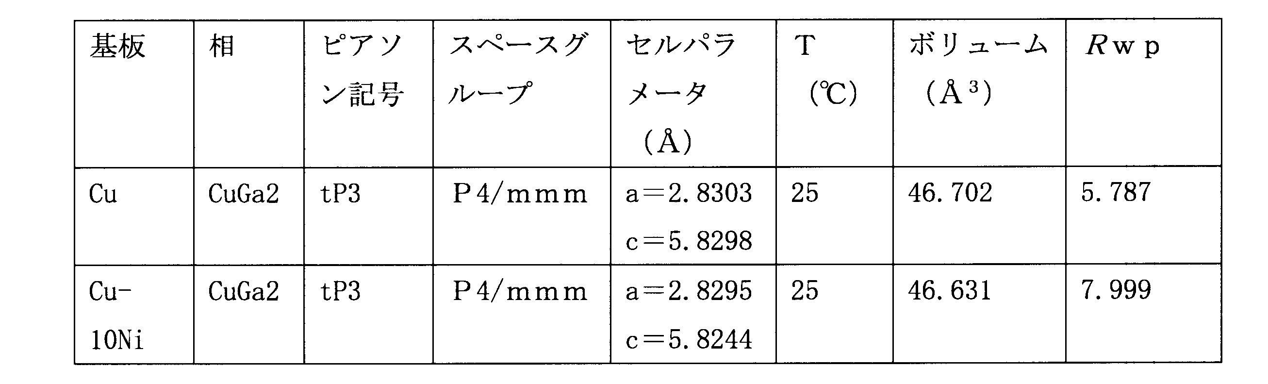
図18(a)、図(b)、図(c)に加熱中のGa/Cu-10Ni反応からのCuGa2のパターンの比較を示す。おれらのパターンの比較から、Cu-10Ni基板で形成されたCuGa2は25℃~300℃の温度範囲にわたって安定していた。
また、Cu基板で形成されたCuGa2は、温度が260℃から300℃に上昇すると、γ3-Cu9Ga4とGaを形成する反応を起こした。
したがって、Cu基板中にNiが含有されている場合には、形成されるIMCは高温にさらされても状態が維持されたものであることがわかる。
また、Cu基板で形成されたCuGa2は、温度が260℃から300℃に上昇すると、γ3-Cu9Ga4とGaを形成する反応を起こした。
したがって、Cu基板中にNiが含有されている場合には、形成されるIMCは高温にさらされても状態が維持されたものであることがわかる。
(実施例2)
以下の手順で、HCl水溶液を用いたはんだ接合を行った。
1)Gaインゴットと5%HCl水溶液を、水浴を使用して35~40℃に加熱した。
Gaインゴットは溶解して液体Gaとなった。
2)各Cu-xNiシート(x=0、2、6、10、14%、長さ25mm、幅5mm、厚み1mm)上に永久マーカーを使用して線を引き、端部から5mmの領域(5mm×5mm)を接合領域として区別した。
3)Cu-xNiシートを5%HCl水溶液に浸漬した。
4)第1のCu-xNiシートに液体Gaを滴下して、5×5mmの接合領域を濡らした後、余分なGaをピペットで吸い戻し、第1のCu-xNiシートの表面に付着したGaの薄い層を残した。なお、Gaは、永久マーカーで作成された線を超えて、または第1のCu-xNiシートの端を超えて、自然に濡れなかった。
上記のプロセスを第2のCu-xNiシートで繰り返し、第1および第2のCu-xNiシートをHCl溶液に浸したままにした。
5)第1および第2のCu-xNiシート基板をHCl溶液中に浸漬している間に、ピンセットを用いて、2枚のCu-xNiシートのGaが塗布された領域どうしを向かい合わせに結合することにより、はんだ接合部(Cu-xNi/Ga/Cu-xNi)を得た。
6)はんだ接合部をHCl溶液から取り出し、室温のエタノールですすいだ。エタノールが気化して、温度が下がると、はんだ接合部のGaはすぐに固化した。
7)はんだ接合部においてIMCの成長を促すために、はんだ接合部のサンプルを30±3℃のアニーリングオーブンに7日間入れた。また、ステーショナリークリップを使用して、焼きなまし中にはんだ接合部に圧力をかけた。
以下の手順で、HCl水溶液を用いたはんだ接合を行った。
1)Gaインゴットと5%HCl水溶液を、水浴を使用して35~40℃に加熱した。
Gaインゴットは溶解して液体Gaとなった。
2)各Cu-xNiシート(x=0、2、6、10、14%、長さ25mm、幅5mm、厚み1mm)上に永久マーカーを使用して線を引き、端部から5mmの領域(5mm×5mm)を接合領域として区別した。
3)Cu-xNiシートを5%HCl水溶液に浸漬した。
4)第1のCu-xNiシートに液体Gaを滴下して、5×5mmの接合領域を濡らした後、余分なGaをピペットで吸い戻し、第1のCu-xNiシートの表面に付着したGaの薄い層を残した。なお、Gaは、永久マーカーで作成された線を超えて、または第1のCu-xNiシートの端を超えて、自然に濡れなかった。
上記のプロセスを第2のCu-xNiシートで繰り返し、第1および第2のCu-xNiシートをHCl溶液に浸したままにした。
5)第1および第2のCu-xNiシート基板をHCl溶液中に浸漬している間に、ピンセットを用いて、2枚のCu-xNiシートのGaが塗布された領域どうしを向かい合わせに結合することにより、はんだ接合部(Cu-xNi/Ga/Cu-xNi)を得た。
6)はんだ接合部をHCl溶液から取り出し、室温のエタノールですすいだ。エタノールが気化して、温度が下がると、はんだ接合部のGaはすぐに固化した。
7)はんだ接合部においてIMCの成長を促すために、はんだ接合部のサンプルを30±3℃のアニーリングオーブンに7日間入れた。また、ステーショナリークリップを使用して、焼きなまし中にはんだ接合部に圧力をかけた。
(実施例3)
以下の手順で、アルゴン雰囲気下ではんだ接合を行った。
1)Gaインゴットと5%HCl水溶液を、水浴を使用して35~40℃に加熱した。
Gaインゴットは溶解して液体Gaとなった。
2)各Cu-xNiシート(x=0、2、6、10、14%、長さ25mm、幅5mm、厚み1mm)上に永久マーカーを使用して線を引き、端部から5mmの領域(5mm×5mm)を接合領域として区別した。
3)Cu-xNiシートをBaker社のフラックス(市販の塩化亜鉛/塩酸ベースのフラックス)に入れ、エタノールで洗浄して酸化物やその他の汚染物を除去した。
4)液体Gaおよび洗浄済みCu-xNiシートをアルゴン充填グローブボックス(O2<0.1ppm、H2O<1ppm、27‐30℃)に移した。
5)液体Gaを第1のCu-xNiシートに滴下して塗布し、5mm×5mmの接合領域を濡らした後、余分な液体Gaをピペットで吸い戻し、第1のCu-xNiシートの表面に付着したGaの薄い層を残した。
6)ピンセットを用いて、第1のCu-xNiシートのGaが塗布された領域に第2の塗布領域を向かい合わせに結合することにより、はんだ接合部(Cu-xNi/Ga/Cu-xNi)を得た。
7)得られたはんだ接合部をグローブボックスから取り出した。
8)IMCの成長を考慮して、はんだ接合部を30±3℃のアニーリングオーブンに7日間入れた。また、ステーショナリークリップを使用して、焼きなまし中にジョイントに圧力をかけた。
以下の手順で、アルゴン雰囲気下ではんだ接合を行った。
1)Gaインゴットと5%HCl水溶液を、水浴を使用して35~40℃に加熱した。
Gaインゴットは溶解して液体Gaとなった。
2)各Cu-xNiシート(x=0、2、6、10、14%、長さ25mm、幅5mm、厚み1mm)上に永久マーカーを使用して線を引き、端部から5mmの領域(5mm×5mm)を接合領域として区別した。
3)Cu-xNiシートをBaker社のフラックス(市販の塩化亜鉛/塩酸ベースのフラックス)に入れ、エタノールで洗浄して酸化物やその他の汚染物を除去した。
4)液体Gaおよび洗浄済みCu-xNiシートをアルゴン充填グローブボックス(O2<0.1ppm、H2O<1ppm、27‐30℃)に移した。
5)液体Gaを第1のCu-xNiシートに滴下して塗布し、5mm×5mmの接合領域を濡らした後、余分な液体Gaをピペットで吸い戻し、第1のCu-xNiシートの表面に付着したGaの薄い層を残した。
6)ピンセットを用いて、第1のCu-xNiシートのGaが塗布された領域に第2の塗布領域を向かい合わせに結合することにより、はんだ接合部(Cu-xNi/Ga/Cu-xNi)を得た。
7)得られたはんだ接合部をグローブボックスから取り出した。
8)IMCの成長を考慮して、はんだ接合部を30±3℃のアニーリングオーブンに7日間入れた。また、ステーショナリークリップを使用して、焼きなまし中にジョイントに圧力をかけた。
(試験例7)
実施例2、3で得られたはんだ接合部のサンプルのせん断強度をインストロン5584引張試験機、10kNロードセルを用いて測定した。
試験条件は、以下のとおり。
ひずみ速度:0.5mm/min、最大荷重:1000N、接着面積:5×5mm
実施例2、3で得られたはんだ接合部のサンプルのせん断強度をインストロン5584引張試験機、10kNロードセルを用いて測定した。
試験条件は、以下のとおり。
ひずみ速度:0.5mm/min、最大荷重:1000N、接着面積:5×5mm
得られた試験結果を表4および図19に示す。
表4および図19の結果より、Cu、Cu-2Ni、Cu-6Niの金属基材同士を用いたはんだ接合部については、HCl法を使用した場合のせん断強度が、グローブボックス法を使用して得られたものよりも高くなっていた。
また、Cu-10Ni、Cu-14Niの金属基材同士を用いたはんだ接合部では、HCl法、グローブボックス法いずれもせん断強度は実施品として合格レベルのものであった。なお、表中、「Force」はフォース、「Stdev」は標準偏差、「Strength」は強度を示す。
表4および図19の結果より、Cu、Cu-2Ni、Cu-6Niの金属基材同士を用いたはんだ接合部については、HCl法を使用した場合のせん断強度が、グローブボックス法を使用して得られたものよりも高くなっていた。
また、Cu-10Ni、Cu-14Niの金属基材同士を用いたはんだ接合部では、HCl法、グローブボックス法いずれもせん断強度は実施品として合格レベルのものであった。なお、表中、「Force」はフォース、「Stdev」は標準偏差、「Strength」は強度を示す。
また、実施例2、3で得られたはんだ接合部の微細構造を、日立3030走査型電子顕微鏡を使用して観察した。その際に、EDSメソッドを使用して、未湿潤のCu基板領域を確認したところ、実施例2で得られたはんだ接合部の微細構造では、実施例3のグローブボックス法を使用した場合よりも、未湿潤領域は小さくなる傾向があることがわかった。
Claims (8)
- 第1金属基材と第2金属基材とをはんだにより接合するはんだ接合部の製造方法であって、
第1金属基材及び第2金属基材のうち少なくとも一方の金属基材が、Ni含量が0重量%以上、44重量%未満、Cu含量が56重量%超である合金であり、
はんだが、Ga及び不可避不純物からなるはんだ合金又はGaを主成分とする融点が30℃以下のはんだ合金であり、
第1金属基材の表面に、はんだを塗布した後、塗布したはんだ上に第2金属基材を載せる工程、
希ガス雰囲気下もしくは大気雰囲気下もしくは液体中で、90℃以下の温度に加熱して第1金属基材と第2金属基材の間にCuGa2又は(Cu、Ni)Ga2を生成させて、第1及び第2金属材料を接合する工程を含む、はんだ接合部の製造方法。 - 第2金属基材の表面にもはんだを塗布し、第1金属基材のはんだ塗布面と第2金属基材のはんだ塗布面とを向かい合わせて接触させる工程を有する請求項1に記載のはんだ接合部の製造方法。
- 第1又は第2金属基材の表面に、はんだを直接載置する請求項1または2に記載のはんだ接合部の製造方法。
- 第1及び第2金属基材が、Ni含量が0重量%超、44重量%未満、Cu含量が56重量%超であるCu-Ni合金である請求項1~3の何れかに記載のはんだ接合部の製造方法。
- 希ガスがアルゴンガスあるいは窒素ガスである請求項1~4の何れか1項に記載のはんだ接合部の製造方法。
- 前記液体が、温水または無機酸の水溶液である、請求項1~4の何れか1項に記載のはんだ接合部の製造方法。
- 第1及び第2金属基材のうち、一方が電子回路基板に形成されている配線であり、他方が電子部品の端子である、請求項1~5の何れか1項に記載のはんだ接合部の製造方法。
- 第1金属基材と第2金属基材がはんだ層を介して接合されているはんだ接合部であって、
第1金属基材及び第2金属基材のうち少なくとも一方の金属基材が、Ni含量が0重量%以上、44重量%未満、Cu含量が56重量%超である合金であり、
はんだ層が、Cu、Ni及びGaの金属間化合物の連続相からなり、かつ、CuGa2又は(Cu、Ni)Ga2を含む、はんだ接合部。
Priority Applications (2)
| Application Number | Priority Date | Filing Date | Title |
|---|---|---|---|
| JP2020556023A JP7482415B2 (ja) | 2018-11-16 | 2019-10-31 | はんだ接合部及びその製造方法 |
| US17/294,379 US11980974B2 (en) | 2018-11-16 | 2019-10-31 | Solder joint part and method for manufacturing the same |
Applications Claiming Priority (4)
| Application Number | Priority Date | Filing Date | Title |
|---|---|---|---|
| JP2018215247 | 2018-11-16 | ||
| JP2018-215247 | 2018-11-16 | ||
| JP2019045284 | 2019-03-12 | ||
| JP2019-045284 | 2019-03-12 |
Publications (1)
| Publication Number | Publication Date |
|---|---|
| WO2020100614A1 true WO2020100614A1 (ja) | 2020-05-22 |
Family
ID=70731501
Family Applications (1)
| Application Number | Title | Priority Date | Filing Date |
|---|---|---|---|
| PCT/JP2019/042814 Ceased WO2020100614A1 (ja) | 2018-11-16 | 2019-10-31 | はんだ接合部及びその製造方法 |
Country Status (3)
| Country | Link |
|---|---|
| US (1) | US11980974B2 (ja) |
| JP (1) | JP7482415B2 (ja) |
| WO (1) | WO2020100614A1 (ja) |
Cited By (1)
| Publication number | Priority date | Publication date | Assignee | Title |
|---|---|---|---|---|
| JP2023108672A (ja) * | 2022-01-26 | 2023-08-07 | パナソニックIpマネジメント株式会社 | 接合材料及び該接合材料を用いた接合構造体 |
Citations (5)
| Publication number | Priority date | Publication date | Assignee | Title |
|---|---|---|---|---|
| JP2007179922A (ja) * | 2005-12-28 | 2007-07-12 | Nikko Fuji Electronics Co Ltd | 半田吸い上がりバリア部を持つ端子及びその製造方法 |
| JP2016051810A (ja) * | 2014-08-29 | 2016-04-11 | 株式会社日本スペリア社 | 導電性接合体 |
| JP2016050324A (ja) * | 2014-08-29 | 2016-04-11 | Jx金属株式会社 | キャリア付銅箔の製造方法、銅張積層板の製造方法、プリント配線板の製造方法、及び、電子機器及びキャリア付銅箔 |
| US20160366760A1 (en) * | 2015-06-10 | 2016-12-15 | Industry Foundation Of Chonnam National University | Stretchable circuit board and method of manufacturing the same |
| US9704964B1 (en) * | 2016-05-26 | 2017-07-11 | The United States Of America As Represented By The Secretary Of The Navy | Graphene-based device with liquid metal contacts |
Family Cites Families (3)
| Publication number | Priority date | Publication date | Assignee | Title |
|---|---|---|---|---|
| US6343647B2 (en) * | 2000-01-11 | 2002-02-05 | Thermax International, Ll.C. | Thermal joint and method of use |
| JP2001198692A (ja) | 2000-01-12 | 2001-07-24 | Matsushita Electric Ind Co Ltd | 光モジュールの接合材料およびこれを用いる光学ヘッド |
| CN101934438A (zh) | 2005-08-18 | 2011-01-05 | 千住金属工业株式会社 | 无铅低温焊料 |
-
2019
- 2019-10-31 JP JP2020556023A patent/JP7482415B2/ja active Active
- 2019-10-31 US US17/294,379 patent/US11980974B2/en active Active
- 2019-10-31 WO PCT/JP2019/042814 patent/WO2020100614A1/ja not_active Ceased
Patent Citations (5)
| Publication number | Priority date | Publication date | Assignee | Title |
|---|---|---|---|---|
| JP2007179922A (ja) * | 2005-12-28 | 2007-07-12 | Nikko Fuji Electronics Co Ltd | 半田吸い上がりバリア部を持つ端子及びその製造方法 |
| JP2016051810A (ja) * | 2014-08-29 | 2016-04-11 | 株式会社日本スペリア社 | 導電性接合体 |
| JP2016050324A (ja) * | 2014-08-29 | 2016-04-11 | Jx金属株式会社 | キャリア付銅箔の製造方法、銅張積層板の製造方法、プリント配線板の製造方法、及び、電子機器及びキャリア付銅箔 |
| US20160366760A1 (en) * | 2015-06-10 | 2016-12-15 | Industry Foundation Of Chonnam National University | Stretchable circuit board and method of manufacturing the same |
| US9704964B1 (en) * | 2016-05-26 | 2017-07-11 | The United States Of America As Represented By The Secretary Of The Navy | Graphene-based device with liquid metal contacts |
Non-Patent Citations (1)
| Title |
|---|
| SHIQIAN LIU ET AL: "Ga-Based Alloys in Microelectronic Interconnects: A Review", MATERIALS, vol. 11, no. 8, 1384, 8 August 2018 (2018-08-08), pages 1 - 20, XP055608383, DOI: 10.3390/ma11081384 * |
Cited By (2)
| Publication number | Priority date | Publication date | Assignee | Title |
|---|---|---|---|---|
| JP2023108672A (ja) * | 2022-01-26 | 2023-08-07 | パナソニックIpマネジメント株式会社 | 接合材料及び該接合材料を用いた接合構造体 |
| JP7847302B2 (ja) | 2022-01-26 | 2026-04-17 | パナソニックIpマネジメント株式会社 | 接合材料及び該接合材料を用いた接合構造体 |
Also Published As
| Publication number | Publication date |
|---|---|
| JPWO2020100614A1 (ja) | 2021-10-14 |
| US20220009040A1 (en) | 2022-01-13 |
| US11980974B2 (en) | 2024-05-14 |
| JP7482415B2 (ja) | 2024-05-14 |
Similar Documents
| Publication | Publication Date | Title |
|---|---|---|
| Zribi et al. | The growth of intermetallic compounds at Sn-Ag-Cu solder/Cu and Sn-Ag-Cu solder/Ni interfaces and the associated evolution of the solder microstructure | |
| Liu et al. | Properties of CuGa2 Formed Between Liquid Ga and Cu Substrates at Room Temperature: Liu, McDonald, Gu, Matsumura, Qu, Sweatman, Nishimura, and Nogita | |
| Pang et al. | Intermetallic growth studies on Sn-Ag-Cu lead-free solder joints | |
| Takaku et al. | Interfacial reaction between Cu substrates and Zn-Al base high-temperature Pb-free solders | |
| TWI638366B (zh) | 半導體裝置用接合導線 | |
| US9101065B2 (en) | Ceramic circuit board and process for producing same | |
| US9263166B2 (en) | Shell activated sintering of core-shell particles | |
| US10399186B2 (en) | Lead-free eutectic solder alloy comprising zinc as the main component and aluminum as an alloying metal | |
| Lee et al. | Influence of Pd (P) thickness on the Pd-free solder reaction between eutectic Sn-Ag alloy and Au/Pd (P)/Ni (P)/Cu multilayer | |
| JP7482415B2 (ja) | はんだ接合部及びその製造方法 | |
| KR102040278B1 (ko) | 무연솔더 합금 조성물 및 그 제조방법, 무연솔더 합금 조성물을 이용한 부재 간의 접합방법 | |
| Wang et al. | Kinetics of intermetallic compound formation at 91Sn–8.55 Zn–0.45 Al lead-free solder alloy/Cu interface | |
| Wu et al. | Bonding silicon chips to aluminum substrates using Ag–In system without flux | |
| Wei et al. | Effect of thermal ageing on (Sn-Ag, Sn-Ag-Zn)/PtAg, Cu/Al2O3 solder joints | |
| KR20180066268A (ko) | 도금용 땜납 합금 및 전자부품 | |
| Pinizzotto et al. | The dependence of the activation energies of intermetallic formation on the composition of composite Sn/Pb solders | |
| Zhu et al. | Active brazing alloy paste as a totally metal thick film conductor material | |
| Dybeł et al. | Graphene-covered copper substrates for soldering applications: Experimental and atomistic insights into interfacial reactions and wetting with SAC305 | |
| Zhang et al. | Growth Behavior of Meta-Stable ${\rm NiSn} _ {3} $ Intermetallic Compound and Its Potential Influence on the Reliability of Electronic Components | |
| Mahmudi et al. | Effects of Ag and Al additions on the structure and creep properties of Sn-9Zn solder alloy | |
| Natzke et al. | Thin layer Ag-Sn transient liquid phase bonding using magnetron sputtering for chip to baseplate bonding | |
| Hlina et al. | Comparison of copper and silver thick film on alumina substrates properties | |
| Young et al. | Microstructural evolution in the Sn-Cu-Ni and Pb-Sn solder joints with Cu and Pt-Ag metallized Al2O3 substrate | |
| Frear et al. | Analysis of the reaction between 60Sn-40Pb solder with a Pd-Pt-Ag-Cu-Au alloy | |
| JP7196706B2 (ja) | 接合用シート及びこの接合用シートを用いて電子部品を基板に接合する方法 |
Legal Events
| Date | Code | Title | Description |
|---|---|---|---|
| 121 | Ep: the epo has been informed by wipo that ep was designated in this application |
Ref document number: 19883939 Country of ref document: EP Kind code of ref document: A1 |
|
| ENP | Entry into the national phase |
Ref document number: 2020556023 Country of ref document: JP Kind code of ref document: A |
|
| NENP | Non-entry into the national phase |
Ref country code: DE |
|
| 122 | Ep: pct application non-entry in european phase |
Ref document number: 19883939 Country of ref document: EP Kind code of ref document: A1 |