WO2020084811A1 - 赤外線センサ - Google Patents
赤外線センサ Download PDFInfo
- Publication number
- WO2020084811A1 WO2020084811A1 PCT/JP2019/013012 JP2019013012W WO2020084811A1 WO 2020084811 A1 WO2020084811 A1 WO 2020084811A1 JP 2019013012 W JP2019013012 W JP 2019013012W WO 2020084811 A1 WO2020084811 A1 WO 2020084811A1
- Authority
- WO
- WIPO (PCT)
- Prior art keywords
- infrared sensor
- infrared
- light guide
- guide member
- opening
- Prior art date
- Legal status (The legal status is an assumption and is not a legal conclusion. Google has not performed a legal analysis and makes no representation as to the accuracy of the status listed.)
- Ceased
Links
Images




Classifications
-
- G—PHYSICS
- G01—MEASURING; TESTING
- G01J—MEASUREMENT OF INTENSITY, VELOCITY, SPECTRAL CONTENT, POLARISATION, PHASE OR PULSE CHARACTERISTICS OF INFRARED, VISIBLE OR ULTRAVIOLET LIGHT; COLORIMETRY; RADIATION PYROMETRY
- G01J1/00—Photometry, e.g. photographic exposure meter
- G01J1/02—Details
-
- G—PHYSICS
- G01—MEASURING; TESTING
- G01J—MEASUREMENT OF INTENSITY, VELOCITY, SPECTRAL CONTENT, POLARISATION, PHASE OR PULSE CHARACTERISTICS OF INFRARED, VISIBLE OR ULTRAVIOLET LIGHT; COLORIMETRY; RADIATION PYROMETRY
- G01J1/00—Photometry, e.g. photographic exposure meter
- G01J1/02—Details
- G01J1/04—Optical or mechanical part supplementary adjustable parts
Definitions
- the present invention relates to an infrared sensor that detects infrared rays from a measurement target and measures the temperature of the measurement target.
- an infrared sensor is placed facing the object to be measured and receives the radiant heat to measure the temperature.
- an infrared sensor is placed facing the object to be measured and receives the radiant heat to measure the temperature.
- a resin film provided on a holder having a light guide portion, an infrared detecting heat sensitive element provided on the resin film for detecting infrared rays through the light guide portion, and a resin film are provided.
- an infrared temperature sensor provided with a temperature-compensating thermosensitive element that is provided in a light-shielded state and detects the temperature of a holder.
- Patent Document 2 proposes an infrared sensor device that includes an infrared sensor element and a visual field control unit that has an opening and covers a part of the visual field of the infrared sensor element.
- a light guide path member is installed as a light guide section or a view control section in order to limit the incidence of radiant heat from the outside at a constant viewing angle.
- Patent Document 3 describes an infrared sensor in which a sensor body having a heat-sensitive element for detection and compensation is installed in a light guide member having a rectangular tube shape.
- the above-mentioned conventional technique has the following problems.
- the sensor body having the detecting heat sensitive element and the compensating heat sensitive element is installed in the light guide member, but the detecting heat sensitive element and the compensating member arranged in the light guide member are provided.
- the detecting heat sensitive element and the compensating member arranged in the light guide member are provided.
- the present invention has been made in view of the above-described problems, and an infrared sensor capable of improving the sensitivity by easily making a temperature difference between the detection heat-sensitive element and the compensation heat-sensitive element in the light guide member.
- the purpose is to provide.
- the infrared sensor according to the first aspect of the present invention includes a mounting substrate having an upper surface disposed on the infrared light receiving side, an infrared sensor main body provided on the upper surface of the mounting substrate, and the infrared sensor installed on the upper surface of the mounting substrate.
- a cylindrical light guide member having an opening above the sensor body and covering the periphery of the infrared sensor body, wherein the infrared sensor body is an insulating substrate and a detecting member provided on the insulating substrate.
- the heat-sensitive element for detection is arranged in the light-receiving region or directly below it, and the heat-sensitive element for compensation is arranged directly under the infrared shielding part
- the light guide member has a rectangular front shape. It is a rectangular tube shape having an opening, the light receiving region is arranged in the center of the light guide member, and the infrared shielding portion is arranged on one side in the long side direction of the opening, and the mounting is performed.
- the upper surface of the substrate is exposed to a wider side than the one side in the long side direction of the opening.
- the light receiving region is arranged in the center of the light guide member, the infrared shielding portion is arranged on one side in the long side direction of the opening, and the upper surface of the mounting substrate is opened in the light guide member. Since it is exposed more widely on one side than on the other side in the direction of the long side of the portion, a temperature difference between the detection heat-sensitive element and the compensation heat-sensitive element in the light guide member is likely to occur. That is, although one side in the long side direction of the opening in the light guide member is covered with an infrared shielding portion, a large part of the upper surface of the mounting board is covered and the temperature is lowered without absorbing infrared rays.
- the upper surface of the mounting board is widely exposed together with the light receiving area, and a large amount of infrared rays are absorbed, so that the temperature becomes high. Therefore, the temperature difference between the infrared ray shielding portion side (compensation side) and the light receiving area side (detection side) is likely to occur, and the sensitivity can be improved.
- An infrared sensor is the infrared sensor according to the first aspect, wherein the mounting substrate includes a plurality of board-side wirings on an upper surface thereof, and the board-side wirings are in the long side direction of the opening in the light guide member. And is disposed on the upper surface of the mounting board so as to be longer on one side than on the other side.
- the board-side wiring is arranged on the upper surface of the mounting board longer than one side in the long side direction of the opening in the light guide member, the long side of the opening.
- the board-side wiring that extends long on one side in the direction absorbs more infrared rays than the other side, and the upper surface of the mounting board exposed on one side in the long side direction of the opening is further warmed and compensated. It becomes easier to make a temperature difference between the detection side and the detection side.
- An infrared sensor according to a third invention is the infrared sensor according to the first or second invention, wherein the infrared sensor body is mounted on the mounting substrate via a base member, and the base member is wider than the insulating substrate. It is characterized in that it has an upper surface and is mounted near the one side in the long side direction of the opening in the light guide member. That is, in this infrared sensor, since the base member has the upper surface wider than the insulating substrate and is mounted near the one side in the long side direction of the opening in the light guide member, the base member is mounted. As a result, the number of mounting substrates exposed on one side in the long side direction of the opening in the light guide member is further reduced, and a temperature difference is more likely to occur.
- the present invention has the following effects. That is, according to the infrared sensor of the present invention, the light receiving area is arranged in the center of the light guide member, the infrared shielding portion is arranged on one side in the long side direction of the opening, and the upper surface of the mounting substrate is In the light guide member, since it is exposed to the other side more than the one side in the long side direction of the opening in the light guide member, the temperature difference between the detection heat-sensitive element and the compensation heat-sensitive element in the light guide member is likely to occur. Become. That is, one side in the long side direction of the opening in the light guide member has a lower temperature, while the light receiving region in the light guide member and the other side have a higher temperature because they absorb much infrared light. Therefore, in the infrared sensor of the present invention, the temperature difference between the infrared shielding portion side (compensation side) and the light receiving region side (detection side) in the light guide member is easily caused, and the sensitivity can be improved.
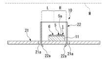
- FIG. 2 is a sectional view taken along the line AA of FIG. 1.
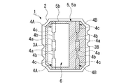
- FIG. 3 is a plan view showing an infrared sensor main body mounted on a base member in the present embodiment.
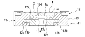
- FIG. 5 is a sectional view taken along line BB of FIG. 4.
- FIG. 3 is a plan view showing an infrared sensor main body in the present embodiment. It is a top view which shows a base member in this embodiment.
- the infrared sensor 10 includes a mounting board 21, an infrared sensor body 1 provided on the upper surface of the mounting board 21 via a base member 11, and an upper surface of the mounting board 21. And a cylindrical light guide member 22 having an opening 22b above the infrared sensor body 1 and covering the periphery of the infrared sensor body 1.
- the infrared sensor main body 1 is provided on the insulating substrate 2, the detecting thermal element 3A and the compensating thermal element 3B provided on the insulating substrate 2, and the insulating substrate 2.
- the upper surface of the insulating substrate 2 is provided with an infrared ray receiving region 6 in which the infrared ray is not blocked by the infrared ray shielding portion 5.
- the detecting heat-sensitive element 3A is arranged directly below the light receiving region 6, and the compensating heat-sensitive element 3B is arranged directly below the infrared shielding portion 5.
- the thermosensitive element for detection 3A and the thermosensitive element for compensation 3B are mounted on the lower surface of the insulating substrate 2.
- the light guide member 22 is in the shape of a rectangular tube having a rectangular opening 22b.
- the light receiving region 6 is arranged in the center of the light guide member 22 in the long side direction of the opening 22b and has a substantially rectangular shape having a long side in the short side direction of the opening 22b. Note that, as shown in FIG. 3, the direction of arrow x is the long side direction of the opening 22b, and the direction of arrow y is the short side direction of the opening 22b.
- the infrared shielding part 5 includes a main shielding part 5a having a compensation heat-sensitive element 3B disposed directly thereunder, and an outer peripheral shielding part 5b extending along the outer edge of the insulating substrate 2 and surrounding the light receiving region 6.
- the main shielding portion 5a is arranged on one side in the long side direction of the opening 22b, and the upper surface of the mounting substrate 21 in the light guide member 22 is located on the other side in the long side direction of the opening 22b. Widely exposed to the side.
- one side in the long side direction of the opening 22b is a right side portion (a portion denoted by reference symbol R) in the opening 22b in FIG. 2, and the other side in the long side direction of the opening 22b is shown in FIG. Is a left side portion (a portion indicated by reference symbol L) in the opening 22b.
- a pair of adhesive electrodes 4a formed on the insulating substrate 2 are connected to one ends of the detection-side wiring 4A and the compensation-side wiring 4B, respectively, and are formed on the insulating substrate 2 at the other ends.
- the terminal electrode 4c is connected.
- the detection-side wiring 4A and the compensation-side wiring 4B each have a connection wiring portion 4b that extends by connecting the adhesive electrode 4a and the terminal electrode 4c.
- the two pairs of terminal electrodes 4c are arranged near the four corners of the insulating substrate 2.
- the terminal portions of the corresponding thermosensitive element for detection 3A and the thermosensitive element for compensation 3B are bonded to the adhesive electrode 4a with a conductive adhesive such as solder.
- the insulating substrate 2 is formed of an insulating film such as a polyimide resin sheet into a substantially rectangular shape or a substantially square shape, and the infrared shielding portion 5, the detection side wiring 4A and the compensation side wiring 4B are formed of copper foil. That is, these are manufactured by a double-sided flexible substrate in which the infrared shielding portion 5, the copper foils as the detection side wiring 4A and the compensation side wiring 4B are pattern-formed on both sides of the polyimide substrate which is the insulating substrate 2. Is.
- the infrared shielding portion 5 is an infrared reflective film formed of a material having an infrared reflectance higher than that of the insulating substrate 2.
- a copper plating is applied with a gold plating film to form a pattern.
- a mirror-finished aluminum vapor deposition film or an aluminum foil may be used. 1 and 3, the infrared shielding portion 5 is hatched.
- thermosensitive element for detection 3A and the thermosensitive element for compensation 3B are chip thermistors having terminals formed on both ends.
- the thermistor there are NTC type, PTC type, CTR type thermistors, etc., but in the present embodiment, for example, an NTC type thermistor is adopted as the detection heat sensitive element 3A and the compensation heat sensitive element 3B.
- This thermistor is made of a thermistor material such as Mn—Co—Cu based material or Mn—Co—Fe based material.
- the mounting board 21 has a plurality of board-side wirings 23 connected to the detection heat-sensitive element 3A or the compensation heat-sensitive element 3B via the terminal member 13 and the detection-side wiring 4A on the upper surface.
- the board-side wiring 23 is arranged on the upper surface of the mounting board 21 in the light guide member 22 longer than one side (right side in FIG. 1) in the long side direction of the opening 22b to the other side (left side in FIG. 1). Has been done.
- a pad portion 23a is formed at an end of the board-side wiring 23 for connection with an external wiring.
- a plurality of through holes 21 a for mounting the light guide member 22 are formed in the mounting substrate 21.
- the mounting board 21 is, for example, a printed circuit board (PCB) and is formed in a rectangular shape.
- the light guide member 22 has a plurality of fixing claw portions 22a inserted through a plurality of through holes 21a in the lower portion, and a portion of the fixing claw portion 22a protruding from the lower surface of the mounting substrate 21 is bent.
- the fixing claw portions 22a are formed on the lower portions of both side surfaces of the light guide member 22, and the mounting substrate 21 has two through holes 21a corresponding to the two fixing claw portions 22a. Are formed.
- the light guide member 22 has a rectangular tubular shape and is integrally formed of metal or resin together with the fixing claw portion 22a.
- a material for forming the light guide member 22 for example, in the case of metal, a thin metal plate such as stainless steel is adopted, and in the case of resin, polyphenylene sulfide, polyether ether ketone, polycarbonate, polypropylene, vinyl chloride, etc. are adopted.
- the infrared sensor 10 of the present embodiment is arranged so as to face a measurement object M that has a constant width and is long in a constant direction.
- the opening 22b of the light guide member 22 is arranged with its long side direction along the length direction of the measuring object M.
- the measuring object M of this embodiment is a fixing roller used in the image forming apparatus.
- the base member 11 has a substantially rectangular shape or a substantially square shape in plan view, is mounted on the mounting substrate 21, and has the infrared sensor main body 1 mounted on the upper portion thereof.
- the base member 11 has an upper surface wider than that of the insulating substrate 2 and is mounted inside the light guide member 22 toward one side in the long side direction of the opening 22b. That is, like the insulating substrate 2, the base member 11 is also arranged so as to be biased to one side (compensation side) in the long side direction of the opening 22b from the center of the light guide member 22.
- the base member 11 has an insulating base main body 12 formed of resin or the like, and an upper end portion attached to the base main body 12 and a conductive material such as solder on the terminal electrode 4c.
- a plurality of conductive terminal members 13 which are connected by an adhesive material and whose lower surface is connected to the detection side wiring 4A or the compensation side wiring 4B of the mounting substrate 21 by a conductive adhesive material such as solder are provided.
- the terminal member 13 is formed of a material such as a metal having a higher thermal conductivity than the base body 12, and has a terminal pin portion 13a protruding laterally.
- the base body 12 has a terminal member hole 12a formed in a side portion and into which a terminal pin portion 13a is inserted and fixed, and an element housing hole 12c formed in an upper portion and directly below the heat sensitive elements 3A and 3B.
- And has a groove portion 12d penetrating in the lateral direction and communicating with the space directly below the detection heat-sensitive element 3A and the space directly below the compensation heat-sensitive element 3B.
- the base member 11 has an intermediate hole 12e formed in the upper portion between the detection heat-sensitive element 3A and the compensation heat-sensitive element 3B and deeper than the groove 12d.
- the long protruding terminal pin portion 13a is fixed by being inserted and fitted into the long hole-shaped terminal member hole portion 12a.
- the base body 12 has a thin plate-like block shape formed in a substantially rectangular shape or a substantially square shape in a plan view, and the four terminal members 13 are fitted in the vicinity of the four corners, and both sides facing each other. Two terminal members 13 are arranged in each. That is, two portions that support the infrared sensor body 1 are provided on both sides of the base body 12 with a space between each other, and the infrared sensor body 1 is supported and fixed at a total of four locations.
- the infrared sensor body 1 is supported with a gap provided between the infrared sensor body 1 and the base body 12. That is, the terminal member 13 has an upper portion protruding from the upper surface of the base body 12 by a certain amount, and the infrared sensor body 1 connected to the upper end portion by a conductive adhesive such as soldering is floated from the base body 12. Support in the state.
- the terminal member 13 has a terminal slit portion 13b extending under the terminal pin portion 13a in the direction opposite to the protruding direction of the terminal pin portion 13a, and the base body 12 is a terminal insertion portion to be inserted into the terminal slit portion 13b. It has 12b.
- the upper end and the lower end of the terminal member 13 are flat parts for soldering.
- the terminal member 13 has a plate shape formed by stamping, etching, or laser processing a metal plate.
- the light receiving region 6 is arranged in the center of the light guide member 22, and the main shielding portion 5a of the infrared shielding portion 5 is located on one side in the long side direction of the opening 22b. Since the upper surface of the mounting substrate 21 is exposed more widely in the light guide member 22 to the other side than the one side in the long side direction of the opening 22b in the light guide member 22, the detection heat-sensitive member in the light guide member 22. A temperature difference between the element 3A and the compensating thermosensitive element 3B is likely to occur.
- the main shield 5a covers most of the upper surface of the mounting substrate 21 and does not absorb infrared rays.
- the temperature becomes low, the upper surface of the mounting substrate 21 is widely exposed together with the light receiving area 6 in the light receiving area 6 in the light guide member 22 and the other side (the side opposite to the main shielding portion), and a large amount of infrared rays are absorbed.
- the temperature rises. Therefore, the temperature difference between the main shielding portion 5a side (compensation side) and the light receiving region 6 side (detection side) is likely to occur, and the sensitivity can be improved.
- the board-side wiring 23 is arranged on the upper surface of the mounting board 21 in the light guide member 22 longer than one side in the long side direction of the opening 22b, the long side of the opening 22b.
- the board-side wiring 23 extending on one side in the direction absorbs more infrared rays than the other side, so that the upper surface of the mounting board 21 exposed on one side in the long side direction of the opening 22b is further warmed. As a result, the temperature difference between the compensating side and the detecting side can be made easier.
- the base member 11 has an upper surface wider than the insulating substrate 2 and is mounted in the light guide member 22 toward one side in the long side direction of the opening 22b, the base member 11 is mounted. As a result, the mounting substrate 21 exposed on one side in the long side direction of the opening 22b in the light guide member 22 becomes smaller, and the temperature difference is more likely to occur.
- thermosensitive element of the chip thermistor is adopted, but a thermosensitive element formed of a thin film thermistor may be adopted.
- a thermosensitive element formed of a thin film thermistor may be adopted.
- the heat sensitive element a thin film thermistor or a chip thermistor is used as described above, but a pyroelectric element or the like can be adopted in addition to the thermistor.
- the infrared shielding portion is provided on the upper surface of the insulating substrate with copper foil or the like, but the infrared shielding portion may be provided with a plate member or the like on or just above the insulating substrate.
- the detection heat-sensitive element is arranged immediately below the light receiving area, that is, on the lower surface of the insulating substrate, but it may be arranged above the light receiving area. That is, the detection heat sensitive element may be directly mounted on the light receiving region on the upper surface of the insulating substrate.
- SYMBOLS 1 ... Infrared sensor main body, 2 ... Insulating substrate, 3A ... Detection thermal element, 3B ... Compensation thermal element, 4A ... Detection side wiring, 4B ... Compensation side wiring, 5 ... Infrared shielding part, 5a ... Main shielding part, 6 ... Light receiving area, 10 ... Infrared sensor, 11 ... Base member, 21 ... Mounting board, 22 ... Light guide member, 23 ... Board side wiring, M ... Measurement object
Landscapes
- Physics & Mathematics (AREA)
- General Physics & Mathematics (AREA)
- Spectroscopy & Molecular Physics (AREA)
- Photometry And Measurement Of Optical Pulse Characteristics (AREA)
- Radiation Pyrometers (AREA)
Abstract
導光路部材内の検出用感熱素子と補償用感熱素子との温度差をつき易くして、感度を向上させることが可能な赤外線センサを提供する。本発明に係る赤外線センサは、実装基板21と、実装基板に設けられた赤外線センサ本体1と、実装基板上に設置され赤外線センサ本体の上方に開口部22bを有した導光路部材22とを備え、赤外線センサ本体が、絶縁性基板と、絶縁性基板に設けられた検出用感熱素子及び補償用感熱素子と、絶縁性基板の上面に設けられた赤外線遮蔽部5と、絶縁性基板上の赤外線の受光領域6とを備え、導光路部材が、長方形状の開口部を有した角筒状であり、受光領域が導光路部材の中央に配されていると共に、赤外線遮蔽部が開口部の長辺方向で一方の側に配され、実装基板の上面が、導光路部材内において開口部の長辺方向で一方の側よりも他方の側に広く露出している。
Description
本発明は、測定対象物からの赤外線を検出して該測定対象物の温度を測定する赤外線センサに関する。
一般に、複写機やプリンタ等の画像形成装置に使用されている定着ローラ等の測定対象物の温度を測定するために、測定対象物に対向配置させ、その輻射熱を受けて温度を測定する赤外線センサが設置されている。
例えば、特許文献1には、導光部を有した保持体に設置された樹脂フィルムと、該樹脂フィルムに設けられ導光部を介して赤外線を検出する赤外線検出用感熱素子と、樹脂フィルムに遮光状態に設けられ保持体の温度を検出する温度補償用感熱素子とを備えた赤外線温度センサが提案されている。
例えば、特許文献1には、導光部を有した保持体に設置された樹脂フィルムと、該樹脂フィルムに設けられ導光部を介して赤外線を検出する赤外線検出用感熱素子と、樹脂フィルムに遮光状態に設けられ保持体の温度を検出する温度補償用感熱素子とを備えた赤外線温度センサが提案されている。
また、特許文献2には、赤外線センサ素子と、開口部を有し、かつ、赤外線センサ素子の視野の一部を覆う視野制御部とを備えた赤外線センサ装置が提案されている。
これらの赤外線センサでは、外部からの輻射熱の入射を一定の視野角で制限するため、導光部や視野制御部として導光路部材が設置されている。
また、特許文献3には、検出用及び補償用の感熱素子を有したセンサ本体が角筒状の導光路部材内に設置された赤外線センサが記載されている。
これらの赤外線センサでは、外部からの輻射熱の入射を一定の視野角で制限するため、導光部や視野制御部として導光路部材が設置されている。
また、特許文献3には、検出用及び補償用の感熱素子を有したセンサ本体が角筒状の導光路部材内に設置された赤外線センサが記載されている。
上記従来の技術には、以下の課題が残されている。
特許文献3の赤外線センサでは、検出用感熱素子と補償用感熱素子とを有したセンサ本体が導光路部材内に設置されているが、導光路部材内に配された検出用感熱素子と補償用感熱素子との温度差がつき難く、感度をさらに向上させることが難しいという不都合があった。
特許文献3の赤外線センサでは、検出用感熱素子と補償用感熱素子とを有したセンサ本体が導光路部材内に設置されているが、導光路部材内に配された検出用感熱素子と補償用感熱素子との温度差がつき難く、感度をさらに向上させることが難しいという不都合があった。
本発明は、前述の課題に鑑みてなされたもので、導光路部材内の検出用感熱素子と補償用感熱素子との温度差をつき易くして、感度を向上させることが可能な赤外線センサを提供することを目的とする。
本発明は、前記課題を解決するために以下の構成を採用した。すなわち、第1の発明に係る赤外線センサは、赤外線の受光側に上面が配される実装基板と、前記実装基板の上面に設けられた赤外線センサ本体と、前記実装基板の上面に設置され前記赤外線センサ本体の上方に開口部を有して前記赤外線センサ本体の周囲を覆う筒状の導光路部材とを備え、前記赤外線センサ本体が、絶縁性基板と、前記絶縁性基板に設けられた検出用感熱素子及び補償用感熱素子と、前記絶縁性基板の上面又は直上に設けられた赤外線遮蔽部と、前記絶縁性基板の上面で前記赤外線遮蔽部によって赤外線の入射が遮られていない赤外線の受光領域とを備え、前記検出用感熱素子が前記受光領域又はその直下に配されていると共に、前記補償用感熱素子が前記赤外線遮蔽部の直下に配され、前記導光路部材が、長方形状の前記開口部を有した角筒状であり、前記受光領域が前記導光路部材の中央に配されていると共に、前記赤外線遮蔽部が前記開口部の長辺方向で一方の側に配され、前記実装基板の上面が、前記導光路部材内において前記開口部の長辺方向で一方の側よりも他方の側に広く露出していることを特徴とする。
この赤外線センサでは、受光領域が導光路部材の中央に配されていると共に、赤外線遮蔽部が開口部の長辺方向で一方の側に配され、実装基板の上面が、導光路部材内において開口部の長辺方向で一方の側よりも他方の側に広く露出しているので、導光路部材内の検出用感熱素子と補償用感熱素子との温度差がつき易くなる。すなわち、導光路部材内の開口部の長辺方向で一方の側は赤外線遮蔽部で実装基板の上面の多くの部分が覆われて赤外線を吸収せずに温度が低くなるが、導光路部材内の受光領域及びその他方の側(赤外線遮蔽部の反対側)では受光領域と共に実装基板の上面が広く露出して赤外線を多く吸収するために温度が高くなる。したがって、赤外線遮蔽部側(補償側)と受光領域側(検出側)との温度差が付き易くなって感度を向上させることができる。
第2の発明に係る赤外線センサは、第1の発明において、前記実装基板が、上面に複数の基板側配線を備え、前記基板側配線が、前記導光路部材内において前記開口部の長辺方向で一方の側よりも他方の側に長く前記実装基板の上面に配されていることを特徴とする。
すなわち、この赤外線センサでは、基板側配線が、導光路部材内において開口部の長辺方向で一方の側よりも他方の側に長く実装基板の上面に配されているので、開口部の長辺方向で一方の側で長く延在した基板側配線が他方の側よりも多く赤外線を吸収することで、開口部の長辺方向で一方の側に露出する実装基板の上面がさらに暖められて補償側と検出側との温度差をよりつけ易くなる。
すなわち、この赤外線センサでは、基板側配線が、導光路部材内において開口部の長辺方向で一方の側よりも他方の側に長く実装基板の上面に配されているので、開口部の長辺方向で一方の側で長く延在した基板側配線が他方の側よりも多く赤外線を吸収することで、開口部の長辺方向で一方の側に露出する実装基板の上面がさらに暖められて補償側と検出側との温度差をよりつけ易くなる。
第3の発明に係る赤外線センサは、第1又は第2の発明において、前記赤外線センサ本体が、ベース部材を介して前記実装基板上に実装され、前記ベース部材が、前記絶縁性基板よりも広い上面を有していると共に前記導光路部材内において前記開口部の長辺方向で一方の側に寄って実装されていることを特徴とする。
すなわち、この赤外線センサでは、ベース部材が、絶縁性基板よりも広い上面を有していると共に導光路部材内において開口部の長辺方向で一方の側に寄って実装されているので、ベース部材により導光路部材内において開口部の長辺方向で一方の側に露出している実装基板がより少なくなり、さらに温度差がつき易くなる。
すなわち、この赤外線センサでは、ベース部材が、絶縁性基板よりも広い上面を有していると共に導光路部材内において開口部の長辺方向で一方の側に寄って実装されているので、ベース部材により導光路部材内において開口部の長辺方向で一方の側に露出している実装基板がより少なくなり、さらに温度差がつき易くなる。
本発明によれば、以下の効果を奏する。
すなわち、本発明に係る赤外線センサによれば、受光領域が導光路部材の中央に配されていると共に、赤外線遮蔽部が開口部の長辺方向で一方の側に配され、実装基板の上面が、導光路部材内において開口部の長辺方向で一方の側よりも他方の側に広く露出しているので、導光路部材内の検出用感熱素子と補償用感熱素子との温度差がつき易くなる。すなわち、導光路部材内の開口部の長辺方向で一方の側は温度が低くなるが、導光路部材内の受光領域及びその他方の側では赤外線を多く吸収するために温度が高くなる。
したがって、本発明の赤外線センサでは、導光路部材内において赤外線遮蔽部側(補償側)と受光領域側(検出側)との温度差が付き易くなって感度を向上させることができる。
すなわち、本発明に係る赤外線センサによれば、受光領域が導光路部材の中央に配されていると共に、赤外線遮蔽部が開口部の長辺方向で一方の側に配され、実装基板の上面が、導光路部材内において開口部の長辺方向で一方の側よりも他方の側に広く露出しているので、導光路部材内の検出用感熱素子と補償用感熱素子との温度差がつき易くなる。すなわち、導光路部材内の開口部の長辺方向で一方の側は温度が低くなるが、導光路部材内の受光領域及びその他方の側では赤外線を多く吸収するために温度が高くなる。
したがって、本発明の赤外線センサでは、導光路部材内において赤外線遮蔽部側(補償側)と受光領域側(検出側)との温度差が付き易くなって感度を向上させることができる。
以下、本発明に係る赤外線センサの一実施形態を、図1から図7を参照しながら説明する。なお、以下の説明に用いる各図面では、各部材を認識可能又は認識容易な大きさとするために縮尺を適宜変更している。
本実施形態の赤外線センサ10は、図1から図3に示すように、実装基板21と、実装基板21の上面にベース部材11を介して設けられた赤外線センサ本体1と、実装基板21の上面に設置され赤外線センサ本体1の上方に開口部22bを有して赤外線センサ本体1の周囲を覆う筒状の導光路部材22とを備えている。
本実施形態の赤外線センサ10は、図1から図3に示すように、実装基板21と、実装基板21の上面にベース部材11を介して設けられた赤外線センサ本体1と、実装基板21の上面に設置され赤外線センサ本体1の上方に開口部22bを有して赤外線センサ本体1の周囲を覆う筒状の導光路部材22とを備えている。
上記赤外線センサ本体1は、図4及び図6に示すように、絶縁性基板2と、絶縁性基板2に設けられた検出用感熱素子3A及び補償用感熱素子3Bと、絶縁性基板2に設けられ検出用感熱素子3Aに接続された一対の検出側配線4A及び補償用感熱素子3Bに接続された一対の補償側配線4Bと、絶縁性基板2の上面に設けられた赤外線遮蔽部5と、絶縁性基板2の上面で赤外線遮蔽部5によって赤外線の入射が遮られていない赤外線の受光領域6とを備えている。
上記検出用感熱素子3Aは受光領域6の直下に配されていると共に、補償用感熱素子3Bは赤外線遮蔽部5の直下に配されている。本実施形態では、絶縁性基板2の下面に検出用感熱素子3A及び補償用感熱素子3Bが実装されている。
上記導光路部材22は、長方形状の開口部22bを有した角筒状である。
上記受光領域6は、開口部22bの長辺方向において導光路部材22の中央に配されていると共に開口部22bの短辺方向に長辺を有する略長方形状とされている。
なお、図3に示すように、矢印xの方向が開口部22bの長辺方向であり、矢印yの方向が開口部22bの短辺方向である。
上記導光路部材22は、長方形状の開口部22bを有した角筒状である。
上記受光領域6は、開口部22bの長辺方向において導光路部材22の中央に配されていると共に開口部22bの短辺方向に長辺を有する略長方形状とされている。
なお、図3に示すように、矢印xの方向が開口部22bの長辺方向であり、矢印yの方向が開口部22bの短辺方向である。
上記赤外線遮蔽部5は、補償用感熱素子3Bを直下に配した主遮蔽部5aと、絶縁性基板2の外縁に沿って延在し受光領域6を囲んで形成された外周遮蔽部5bとを有している。
上記主遮蔽部5aは、開口部22bの長辺方向で一方の側に配され、実装基板21の上面が、導光路部材22内において開口部22bの長辺方向で一方の側よりも他方の側に広く露出している。なお、開口部22bの長辺方向で一方の側は、図2において開口部22b内の右側の部分(符号Rの部分)であり、開口部22bの長辺方向で他方の側は、図2において開口部22b内の左側の部分(符号Lの部分)である。
上記主遮蔽部5aは、開口部22bの長辺方向で一方の側に配され、実装基板21の上面が、導光路部材22内において開口部22bの長辺方向で一方の側よりも他方の側に広く露出している。なお、開口部22bの長辺方向で一方の側は、図2において開口部22b内の右側の部分(符号Rの部分)であり、開口部22bの長辺方向で他方の側は、図2において開口部22b内の左側の部分(符号Lの部分)である。
上記検出側配線4A及び補償側配線4Bには、その一端部にそれぞれ絶縁性基板2に形成された一対の接着電極4aが接続されていると共に、他端部にそれぞれ絶縁性基板2に形成された端子電極4cが接続されている。また、検出側配線4A及び補償側配線4Bは、接着電極4aと端子電極4cとを接続して延在する接続配線部4bをそれぞれ有している。
二対の端子電極4cは、絶縁性基板2の四隅近傍に配されている。
なお、上記接着電極4aには、それぞれ対応する検出用感熱素子3A及び補償用感熱素子3Bの端子部が半田等の導電性接着材で接着されている。
二対の端子電極4cは、絶縁性基板2の四隅近傍に配されている。
なお、上記接着電極4aには、それぞれ対応する検出用感熱素子3A及び補償用感熱素子3Bの端子部が半田等の導電性接着材で接着されている。
上記絶縁性基板2は、ポリイミド樹脂シート等の絶縁性フィルムで略長方形状又は略正方形状に形成され、赤外線遮蔽部5,検出側配線4A及び補償側配線4Bが銅箔で形成されている。すなわち、これらは、絶縁性基板2とされるポリイミド基板の両面に、赤外線遮蔽部5,検出側配線4A及び補償側配線4Bとされる銅箔がパターン形成された両面フレキシブル基板によって作製されたものである。
上記赤外線遮蔽部5は、絶縁性基板2よりも高い赤外線反射率を有する材料で形成された赤外線反射膜であり、本実施形態では銅箔上に金メッキ膜が施されてパターン形成されている。なお、金メッキ膜の他に、例えば鏡面のアルミニウム蒸着膜やアルミニウム箔等で形成しても構わない。
なお、図1及び図3において赤外線遮蔽部5には、ハッチングを施している。
なお、図1及び図3において赤外線遮蔽部5には、ハッチングを施している。
上記検出用感熱素子3A及び補償用感熱素子3Bは、両端部に端子部が形成されたチップサーミスタである。このサーミスタとしては、NTC型、PTC型、CTR型等のサーミスタがあるが、本実施形態では、検出用感熱素子3A及び補償用感熱素子3Bとして、例えばNTC型サーミスタを採用している。このサーミスタは、Mn-Co-Cu系材料、Mn-Co-Fe系材料等のサーミスタ材料で形成されている。
上記実装基板21は、端子部材13及び検出側配線4Aを介して検出用感熱素子3A又は補償用感熱素子3Bに接続される複数の基板側配線23を上面に有している。
上記基板側配線23は、導光路部材22内において開口部22bの長辺方向で一方の側(図1の右側)よりも他方の側(図1の左側)に長く実装基板21の上面に配されている。
基板側配線23の端部には、外部配線との接続用にパッド部23aが形成されている。
実装基板21には、導光路部材22取り付け用に複数の貫通孔21aが形成されている。
この実装基板21は、例えばプリント基板(PCB)であり、長方形状に形成されている。
上記基板側配線23は、導光路部材22内において開口部22bの長辺方向で一方の側(図1の右側)よりも他方の側(図1の左側)に長く実装基板21の上面に配されている。
基板側配線23の端部には、外部配線との接続用にパッド部23aが形成されている。
実装基板21には、導光路部材22取り付け用に複数の貫通孔21aが形成されている。
この実装基板21は、例えばプリント基板(PCB)であり、長方形状に形成されている。
上記導光路部材22は、下部に複数の貫通孔21aに挿通された複数の固定用爪部22aを有し、固定用爪部22aの実装基板21の下面から突出した部分が折り曲げられている。
なお、本実施形態では、導光路部材22の両側面の下部に固定用爪部22aが形成されていると共に、実装基板21には、2つの固定用爪部22aに対応した2つの貫通孔21aが形成されている。
なお、本実施形態では、導光路部材22の両側面の下部に固定用爪部22aが形成されていると共に、実装基板21には、2つの固定用爪部22aに対応した2つの貫通孔21aが形成されている。
導光路部材22は、角筒状であり、固定用爪部22aと共に金属または樹脂で一体成形されている。導光路部材22を構成する材質としては、例えば金属の場合、ステンレス等の金属薄板などが採用され、樹脂の場合、ポリフェニレンサルファイド、ポリエーテルエーテルケトン、ポリカーボネート、ポリプロピレン、塩化ビニルなどが採用される。
本実施形態の赤外線センサ10は、図8に示すように、一定の幅で一定の方向に長い測定対象物Mに対向配置されている。
導光路部材22の開口部22bは、その長辺方向を測定対象物Mの長さ方向に沿って配される。
なお、本実施形態の測定対象物Mは、画像形成装置に使用される定着ローラである。
導光路部材22の開口部22bは、その長辺方向を測定対象物Mの長さ方向に沿って配される。
なお、本実施形態の測定対象物Mは、画像形成装置に使用される定着ローラである。
上記ベース部材11は、図7に示すように、平面視で略長方形状又は略正方形状とされ、実装基板21上に実装されていると共に、赤外線センサ本体1を上部に搭載している。
このベース部材11は、絶縁性基板2よりも広い上面を有していると共に導光路部材22内において開口部22bの長辺方向で一方の側に寄って実装されている。すなわち、ベース部材11も、絶縁性基板2と同様に、導光路部材22の中心から開口部22bの長辺方向で一方の側(補償側)に偏って配置されている。
このベース部材11は、絶縁性基板2よりも広い上面を有していると共に導光路部材22内において開口部22bの長辺方向で一方の側に寄って実装されている。すなわち、ベース部材11も、絶縁性基板2と同様に、導光路部材22の中心から開口部22bの長辺方向で一方の側(補償側)に偏って配置されている。
ベース部材11は、図4,図5及び図7に示すように、樹脂等で成形された絶縁性のベース本体12と、ベース本体12に取り付けられ上端部が端子電極4cにはんだ等の導電性接着材で接続されると共に下面が実装基板21の検出側配線4A又は補償側配線4Bにはんだ等の導電性接着材で接続される導電性の複数の端子部材13とを備えている。
上記端子部材13は、ベース本体12より熱伝導性の高い金属等の材料で形成されていると共に、側方に突出した端子ピン部13aを有している。
上記ベース本体12は、側部に形成され端子ピン部13aが差し込み固定される端子部材用穴部12aと、上部に形成され感熱素子3A,3Bの直下に配された素子収納用穴部12cと、横方向に貫通し、検出用感熱素子3Aの直下の空間と補償用感熱素子3Bの直下の空間とに連通している溝部12dとを有している。
また、ベース部材11は、上部に検出用感熱素子3Aと補償用感熱素子3Bとの間に溝部12dよりも深く形成された中間穴部12eを有している。
長く突出した端子ピン部13aは、長孔形状の端子部材用穴部12aに差し込まれて嵌め込まれることで固定される。
上記ベース本体12は、側部に形成され端子ピン部13aが差し込み固定される端子部材用穴部12aと、上部に形成され感熱素子3A,3Bの直下に配された素子収納用穴部12cと、横方向に貫通し、検出用感熱素子3Aの直下の空間と補償用感熱素子3Bの直下の空間とに連通している溝部12dとを有している。
また、ベース部材11は、上部に検出用感熱素子3Aと補償用感熱素子3Bとの間に溝部12dよりも深く形成された中間穴部12eを有している。
長く突出した端子ピン部13aは、長孔形状の端子部材用穴部12aに差し込まれて嵌め込まれることで固定される。
本実施形態では、ベース本体12が平面視で略長方形状又は略正方形状に形成された薄板状のブロック形状であり、4つの端子部材13が4つの角部の近傍に嵌め込まれ、対向する両側にそれぞれ2つずつ端子部材13が配されている。すなわち、ベース本体12の両側にそれぞれ赤外線センサ本体1を支持する部分が2つずつ互いに間隔を空けて設けられ、全部で4箇所で赤外線センサ本体1が支持、固定される。
なお、赤外線センサ本体1は、ベース本体12との間に隙間を設けて支持されている。すなわち、上記端子部材13は、その上部がベース本体12の上面から一定量だけ突出しており、上端部にはんだ付け等の導電性接着材で接続された赤外線センサ本体1をベース本体12から浮かせた状態で支持している。
端子部材13は、端子ピン部13aの下に該端子ピン部13aの突出方向と逆に延在した端子スリット部13bを有し、ベース本体12は、端子スリット部13bに差し込まれる端子用差し込み部12bを有している。
端子部材13の上端部及び下端部は、はんだ付け用に平坦部とされている。
なお、上記端子部材13は、金属板から型抜き加工、エッチング加工又はレーザ加工によって形成された板状である。
端子部材13の上端部及び下端部は、はんだ付け用に平坦部とされている。
なお、上記端子部材13は、金属板から型抜き加工、エッチング加工又はレーザ加工によって形成された板状である。
このように本実施形態の赤外線センサ10では、受光領域6が導光路部材22の中央に配されていると共に、赤外線遮蔽部5の主遮蔽部5aが開口部22bの長辺方向で一方の側に配され、実装基板21の上面が、導光路部材22内において開口部22bの長辺方向で一方の側よりも他方の側に広く露出しているので、導光路部材22内の検出用感熱素子3Aと補償用感熱素子3Bとの温度差がつき易くなる。
すなわち、導光路部材22内の主遮蔽部5a側(開口部22bの長辺方向で一方の側)は主遮蔽部5aで実装基板21の上面の多くの部分が覆われて赤外線を吸収せずに温度が低くなるが、導光路部材22内の受光領域6及びその他方の側(主遮蔽部の反対側)では受光領域6と共に実装基板21の上面が広く露出して赤外線を多く吸収するために温度が高くなる。したがって、主遮蔽部5a側(補償側)と受光領域6側(検出側)との温度差が付き易くなって感度を向上させることができる。
また、基板側配線23が、導光路部材22内において開口部22bの長辺方向で一方の側よりも他方の側に長く実装基板21の上面に配されているので、開口部22bの長辺方向で一方の側で長く延在した基板側配線23が他方の側よりも多く赤外線を吸収することで、開口部22bの長辺方向で一方の側に露出する実装基板21の上面がさらに暖められて補償側と検出側との温度差をよりつけ易くなる。
さらに、ベース部材11が、絶縁性基板2よりも広い上面を有していると共に導光路部材22内において開口部22bの長辺方向で一方の側に寄って実装されているので、ベース部材11により導光路部材22内において開口部22bの長辺方向で一方の側に露出している実装基板21がより少なくなり、さらに温度差がつき易くなる。
さらに、ベース部材11が、絶縁性基板2よりも広い上面を有していると共に導光路部材22内において開口部22bの長辺方向で一方の側に寄って実装されているので、ベース部材11により導光路部材22内において開口部22bの長辺方向で一方の側に露出している実装基板21がより少なくなり、さらに温度差がつき易くなる。
なお、本発明の技術範囲は上記実施形態に限定されるものではなく、本発明の趣旨を逸脱しない範囲において種々の変更を加えることが可能である。
例えば、上記実施形態では、チップサーミスタの感熱素子を採用しているが、薄膜サーミスタで形成された感熱素子を採用しても構わない。
なお、感熱素子としては、上述したように薄膜サーミスタやチップサーミスタが用いられるが、サーミスタ以外に焦電素子等も採用可能である。
また、上記実施形態では、絶縁性基板の上面に銅箔等で赤外線遮蔽部が設けられているが、絶縁性基板の上又は直上に板部材等で赤外線遮蔽部を設けても構わない。
また、上記実施形態では、検出用感熱素子が受光領域の直下、すなわち絶縁性基板の下面に配されているが、受光領域上に配されていても構わない。すなわち、絶縁性基板の上面の受光領域に検出用感熱素子を直接実装しても構わない。
なお、感熱素子としては、上述したように薄膜サーミスタやチップサーミスタが用いられるが、サーミスタ以外に焦電素子等も採用可能である。
また、上記実施形態では、絶縁性基板の上面に銅箔等で赤外線遮蔽部が設けられているが、絶縁性基板の上又は直上に板部材等で赤外線遮蔽部を設けても構わない。
また、上記実施形態では、検出用感熱素子が受光領域の直下、すなわち絶縁性基板の下面に配されているが、受光領域上に配されていても構わない。すなわち、絶縁性基板の上面の受光領域に検出用感熱素子を直接実装しても構わない。
1…赤外線センサ本体、2…絶縁性基板、3A…検出用感熱素子、3B…補償用感熱素子、4A…検出側配線、4B…補償側配線、5…赤外線遮蔽部、5a…主遮蔽部、6…受光領域、10…赤外線センサ、11…ベース部材、21…実装基板、22…導光路部材、23…基板側配線、M…測定対象物
Claims (3)
- 赤外線の受光側に上面が配される実装基板と、
前記実装基板の上面に設けられた赤外線センサ本体と、
前記実装基板の上面に設置され前記赤外線センサ本体の上方に開口部を有して前記赤外線センサ本体の周囲を覆う筒状の導光路部材とを備え、
前記赤外線センサ本体が、絶縁性基板と、前記絶縁性基板に設けられた検出用感熱素子及び補償用感熱素子と、前記絶縁性基板の上面又は直上に設けられた赤外線遮蔽部と、前記絶縁性基板の上面で前記赤外線遮蔽部によって赤外線の入射が遮られていない赤外線の受光領域とを備え、
前記検出用感熱素子が前記受光領域又はその直下に配されていると共に、前記補償用感熱素子が前記赤外線遮蔽部の直下に配され、
前記導光路部材が、長方形状の前記開口部を有した角筒状であり、
前記受光領域が前記導光路部材の中央に配されていると共に、前記赤外線遮蔽部が前記開口部の長辺方向で一方の側に配され、
前記実装基板の上面が、前記導光路部材内において前記開口部の長辺方向で一方の側よりも他方の側に広く露出していることを特徴とする赤外線センサ。 - 請求項1に記載の赤外線センサにおいて、
前記実装基板が、上面に複数の基板側配線を備え、
前記基板側配線が、前記導光路部材内において前記開口部の長辺方向で一方の側よりも他方の側に長く前記実装基板の上面に配されていることを特徴とする赤外線センサ。 - 請求項1に記載の赤外線センサにおいて、
前記赤外線センサ本体が、ベース部材を介して前記実装基板上に実装され、
前記ベース部材が、前記絶縁性基板よりも広い上面を有していると共に前記導光路部材内において前記開口部の長辺方向で一方の側に寄って実装されていることを特徴とする赤外線センサ。
Applications Claiming Priority (2)
| Application Number | Priority Date | Filing Date | Title |
|---|---|---|---|
| JP2018199681A JP2020067348A (ja) | 2018-10-24 | 2018-10-24 | 赤外線センサ |
| JP2018-199681 | 2018-10-24 |
Publications (1)
| Publication Number | Publication Date |
|---|---|
| WO2020084811A1 true WO2020084811A1 (ja) | 2020-04-30 |
Family
ID=70331516
Family Applications (1)
| Application Number | Title | Priority Date | Filing Date |
|---|---|---|---|
| PCT/JP2019/013012 Ceased WO2020084811A1 (ja) | 2018-10-24 | 2019-03-26 | 赤外線センサ |
Country Status (2)
| Country | Link |
|---|---|
| JP (1) | JP2020067348A (ja) |
| WO (1) | WO2020084811A1 (ja) |
Citations (9)
| Publication number | Priority date | Publication date | Assignee | Title |
|---|---|---|---|---|
| JPH11281481A (ja) * | 1998-03-27 | 1999-10-15 | Matsushita Electric Works Ltd | 放射温度検出素子 |
| JP2012068115A (ja) * | 2010-09-23 | 2012-04-05 | Mitsubishi Materials Corp | 赤外線センサ |
| CN102478432A (zh) * | 2010-11-30 | 2012-05-30 | 三菱综合材料株式会社 | 红外线传感器 |
| JP2013113732A (ja) * | 2011-11-29 | 2013-06-10 | Mitsubishi Materials Corp | 赤外線センサ及びこれを備えた誘導加熱調理器 |
| JP2013160635A (ja) * | 2012-02-06 | 2013-08-19 | Mitsubishi Materials Corp | 赤外線センサ及び赤外線センサ装置 |
| JP2013205063A (ja) * | 2012-03-27 | 2013-10-07 | Nec Tokin Corp | 視野角制限カバー及びそれを備えた赤外線センサ |
| JP2014071051A (ja) * | 2012-09-29 | 2014-04-21 | Mitsubishi Materials Corp | 赤外線センサ実装部材 |
| JP2014089108A (ja) * | 2012-10-30 | 2014-05-15 | Tdk Corp | 非接触温度センサ |
| JP2018162982A (ja) * | 2017-03-24 | 2018-10-18 | 三菱マテリアル株式会社 | 赤外線センサ |
-
2018
- 2018-10-24 JP JP2018199681A patent/JP2020067348A/ja active Pending
-
2019
- 2019-03-26 WO PCT/JP2019/013012 patent/WO2020084811A1/ja not_active Ceased
Patent Citations (9)
| Publication number | Priority date | Publication date | Assignee | Title |
|---|---|---|---|---|
| JPH11281481A (ja) * | 1998-03-27 | 1999-10-15 | Matsushita Electric Works Ltd | 放射温度検出素子 |
| JP2012068115A (ja) * | 2010-09-23 | 2012-04-05 | Mitsubishi Materials Corp | 赤外線センサ |
| CN102478432A (zh) * | 2010-11-30 | 2012-05-30 | 三菱综合材料株式会社 | 红外线传感器 |
| JP2013113732A (ja) * | 2011-11-29 | 2013-06-10 | Mitsubishi Materials Corp | 赤外線センサ及びこれを備えた誘導加熱調理器 |
| JP2013160635A (ja) * | 2012-02-06 | 2013-08-19 | Mitsubishi Materials Corp | 赤外線センサ及び赤外線センサ装置 |
| JP2013205063A (ja) * | 2012-03-27 | 2013-10-07 | Nec Tokin Corp | 視野角制限カバー及びそれを備えた赤外線センサ |
| JP2014071051A (ja) * | 2012-09-29 | 2014-04-21 | Mitsubishi Materials Corp | 赤外線センサ実装部材 |
| JP2014089108A (ja) * | 2012-10-30 | 2014-05-15 | Tdk Corp | 非接触温度センサ |
| JP2018162982A (ja) * | 2017-03-24 | 2018-10-18 | 三菱マテリアル株式会社 | 赤外線センサ |
Also Published As
| Publication number | Publication date |
|---|---|
| JP2020067348A (ja) | 2020-04-30 |
Similar Documents
| Publication | Publication Date | Title |
|---|---|---|
| JP5832007B2 (ja) | 赤外線センサ及びその製造方法 | |
| CN104011518B (zh) | 红外线传感器及红外线传感装置 | |
| KR101972196B1 (ko) | 적외선 센서 | |
| JP5736906B2 (ja) | 赤外線センサ | |
| KR20170129755A (ko) | 적외선 온도 센서, 회로 기판 및 적외선 온도 센서를 이용한 장치 | |
| KR20180114043A (ko) | 적외선 센서 장치 | |
| KR20140012697A (ko) | 적외선 센서 | |
| JP6319406B2 (ja) | 赤外線センサ装置 | |
| JP6477058B2 (ja) | 赤外線センサ | |
| WO2020084811A1 (ja) | 赤外線センサ | |
| JP5206484B2 (ja) | 温度センサ | |
| WO2020084809A1 (ja) | 赤外線センサ | |
| JP2017181031A (ja) | 赤外線センサ | |
| JP6741201B2 (ja) | 赤外線センサ | |
| JP2017181130A (ja) | 赤外線センサ装置 | |
| JP6620608B2 (ja) | 赤外線センサ | |
| EP3410084A1 (en) | Infrared sensor | |
| JP2019128178A (ja) | 赤外線センサ | |
| WO2019181717A1 (ja) | 赤外線センサ装置 | |
| JP6743741B2 (ja) | 赤外線センサ | |
| WO2018168663A1 (ja) | 赤外線センサ | |
| JP2020153667A (ja) | 導光路部材及びその製造方法 | |
| JP2018169191A (ja) | 赤外線センサ | |
| JP2018169192A (ja) | 赤外線センサ | |
| JPWO2021100312A1 (ja) | 赤外線温度センサ、温度検出装置、および画像形成装置 |
Legal Events
| Date | Code | Title | Description |
|---|---|---|---|
| 121 | Ep: the epo has been informed by wipo that ep was designated in this application |
Ref document number: 19876587 Country of ref document: EP Kind code of ref document: A1 |
|
| NENP | Non-entry into the national phase |
Ref country code: DE |
|
| 32PN | Ep: public notification in the ep bulletin as address of the adressee cannot be established |
Free format text: NOTING OF LOSS OF RIGHTS PURSUANT TO RULE 112(1) EPC (EPO FORM 1205A DATED 23/07/2021) |
|
| 122 | Ep: pct application non-entry in european phase |
Ref document number: 19876587 Country of ref document: EP Kind code of ref document: A1 |