WO2020084729A1 - 荷電粒子線装置、荷電粒子線装置のオートフォーカス処理方法、及び検出器 - Google Patents
荷電粒子線装置、荷電粒子線装置のオートフォーカス処理方法、及び検出器 Download PDFInfo
- Publication number
- WO2020084729A1 WO2020084729A1 PCT/JP2018/039624 JP2018039624W WO2020084729A1 WO 2020084729 A1 WO2020084729 A1 WO 2020084729A1 JP 2018039624 W JP2018039624 W JP 2018039624W WO 2020084729 A1 WO2020084729 A1 WO 2020084729A1
- Authority
- WO
- WIPO (PCT)
- Prior art keywords
- insulating layer
- conductive layer
- sample chamber
- sample
- signal
- Prior art date
- Legal status (The legal status is an assumption and is not a legal conclusion. Google has not performed a legal analysis and makes no representation as to the accuracy of the status listed.)
- Ceased
Links
Images









Classifications
-
- H—ELECTRICITY
- H01—ELECTRIC ELEMENTS
- H01J—ELECTRIC DISCHARGE TUBES OR DISCHARGE LAMPS
- H01J37/00—Discharge tubes with provision for introducing objects or material to be exposed to the discharge, e.g. for the purpose of examination or processing thereof
- H01J37/02—Details
- H01J37/21—Means for adjusting the focus
-
- H—ELECTRICITY
- H01—ELECTRIC ELEMENTS
- H01J—ELECTRIC DISCHARGE TUBES OR DISCHARGE LAMPS
- H01J37/00—Discharge tubes with provision for introducing objects or material to be exposed to the discharge, e.g. for the purpose of examination or processing thereof
- H01J37/02—Details
- H01J37/244—Detectors; Associated components or circuits therefor
-
- H—ELECTRICITY
- H01—ELECTRIC ELEMENTS
- H01J—ELECTRIC DISCHARGE TUBES OR DISCHARGE LAMPS
- H01J37/00—Discharge tubes with provision for introducing objects or material to be exposed to the discharge, e.g. for the purpose of examination or processing thereof
- H01J37/02—Details
- H01J37/20—Means for supporting or positioning the object or the material; Means for adjusting diaphragms or lenses associated with the support
-
- H—ELECTRICITY
- H01—ELECTRIC ELEMENTS
- H01J—ELECTRIC DISCHARGE TUBES OR DISCHARGE LAMPS
- H01J37/00—Discharge tubes with provision for introducing objects or material to be exposed to the discharge, e.g. for the purpose of examination or processing thereof
- H01J37/26—Electron or ion microscopes; Electron or ion diffraction tubes
- H01J37/261—Details
- H01J37/265—Controlling the tube; circuit arrangements adapted to a particular application not otherwise provided, e.g. bright-field-dark-field illumination
-
- H—ELECTRICITY
- H01—ELECTRIC ELEMENTS
- H01J—ELECTRIC DISCHARGE TUBES OR DISCHARGE LAMPS
- H01J2237/00—Discharge tubes exposing object to beam, e.g. for analysis treatment, etching, imaging
- H01J2237/26—Electron or ion microscopes
- H01J2237/2602—Details
- H01J2237/2605—Details operating at elevated pressures, e.g. atmosphere
- H01J2237/2608—Details operating at elevated pressures, e.g. atmosphere with environmental specimen chamber
Definitions
- the present invention relates to a charged particle beam device and a detector for observing the shape or material of a sample using a detection signal generated by irradiating a charged particle beam. More specifically, the present invention relates to a charged particle beam device and a detector capable of observing a biochemical sample or a liquid sample in a non-invasive state while suppressing changes in state and damage.
- the housing is evacuated, the sample is placed in a vacuum atmosphere, and the sample is imaged. Since the electron beam is scattered by gas molecules such as air and liquid molecules, it is preferable to keep the passage of the electron beam in a vacuum atmosphere.
- the biochemical sample and the liquid sample are damaged or change in state, and it has been considered difficult to observe in a non-invasive state.
- an electron microscope capable of observing a sample to be observed under an atmospheric pressure environment or an in-liquid environment has been developed.
- Patent Document 1 describes an SEM that can be observed while a sample is kept under an atmospheric pressure atmosphere.
- a diaphragm that can transmit an electron beam is provided between the electron optical system and the sample to separate the vacuum state from the atmospheric state.
- the SEM image is obtained by arranging the sample in the vicinity of the atmosphere side of the diaphragm, basically directly irradiating the sample with an electron beam in a state where the sample and the diaphragm are not in contact with each other, and detecting signal electrons generated from the sample.
- the diaphragm acts as a vacuum partition to prevent the electron beam from scattering by maintaining a high vacuum state until the electron beam reaches the diaphragm. Observation is possible by limiting the distance from the diaphragm to the sample.
- Patent Documents 2 and 3 disclose a sample holder and an observation system for observing a biological sample in an aqueous solution in a living state using a scanning electron microscope without performing a staining process or an immobilization process. ing.
- a biological sample with a scanning electron microscope, the interaction between the electron beam and the biological sample is extremely low, so it is common to perform various staining and immobilization treatments in order to improve the contrast of the observed image. there were.
- the biological sample to be observed is destroyed, and it becomes impossible to observe it in a living state.
- a high-energy electron beam is directly applied to the sample, the damage may destroy the biological sample.
- the observation system disclosed in Patent Documents 2 and 3 includes a first insulating film whose one main surface is a holding surface for an observation sample, and a conductive film laminated on the other main surface of the first insulating film.
- An in-liquid sample holder is used to irradiate an electron beam from the side of the conductive film while the conductive film is applied with a ground potential or a predetermined bias voltage. Due to the irradiated electron beam, a local potential change occurs on one main surface of the first insulating film. A signal based on this potential change is detected by a detection electrode provided below the second insulating film arranged on the opposite side of the observation sample.
- the signal based on the potential change generated in the first insulating film propagates through the observation sample and is detected by the detection electrode.
- the signal transmission force at this time differs depending on the observation sample. For example, since water has a high relative permittivity of about 80, it allows signals to propagate well, whereas biological samples have a low relative permittivity of about 2 to 3, which reduces the signal transmission power. Therefore, it is possible to observe the biological sample in the aqueous solution with a high contrast based on the intensity difference of the potential change signal propagated through the observation sample without the dyeing process. This method is suitable for damage-less observation of biological samples in liquid, because it is not necessary to directly apply a high-energy electron beam to the sample to be observed.
- JP 2012-221766 A JP, 2014-203733, A JP, 2016-072184, A
- Patent Document 1 requires a detector as a component for detecting signal electrons. Therefore, there is a possibility that the cost may increase.
- the detection electrode provided below the sample holder is used to detect the potential change signal.
- the sample holder only needs to have a laminated film of a first insulating film and a conductive film on the electron beam irradiation side and a second insulating film on the surfaces facing each other with the observation sample interposed therebetween.
- a layer serving as a frame for maintaining the strength of the sample holder is provided, and the layer serving as the frame is partially processed to form a desired laminated film or to form a second insulating film. It is necessary to expose the elastic membrane.
- the detection electrode provided below the sample holder is used for detecting the potential change signal, it is necessary to process both the upper surface and the lower surface of the sample holder, which may increase the cost.
- the present invention has been made in view of such a problem, and an object thereof is to easily and with a high observation throughput, a biochemical sample or a liquid sample without a staining process or an immobilization process. Another object of the present invention is to provide a charged particle beam device and a detector capable of observing in a non-invasive state while suppressing the above.
- a charged particle beam device includes an electron optical system, a stage, a first insulating layer that holds a sample and is in contact with the sample, and a conductive layer formed on the first insulating layer. And a signal detection circuit connected to the conductive layer for detecting a current flowing in the conductive layer, and a main control unit for controlling the electron optical system and the stage, and the main control unit is the electron optical system. To irradiate the electron beam on the conductive layer of the sample chamber mounted on the stage, and the detection signal from the signal detection circuit is input.
- the charged particle beam device makes it possible to observe a biochemical sample or liquid sample in a non-invasive state without changing the state or damaging it without dyeing or immobilizing treatment.
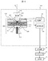
- FIG. 1 shows a block diagram of the scanning electron microscope according to the first embodiment.
- the column 610 incorporates an electron optical system that irradiates a sample to be observed with an electron beam.
- the electron optical system is arranged in the column 610 and focuses the electron gun 11 and the electron beam 12 emitted from the electron gun 11 to irradiate the sample 200 as a minute spot onto the sample lens 200, the objective lens 62, and the electron beam 12 non-contact.
- An astigmatism corrector 61 for correcting point aberration, a deflector 13 for two-dimensionally scanning the electron beam 12 on the sample 200, and an image shift for two-dimensionally shifting the scanning center position of the electron beam 12 on the sample 200.
- Column 610 is maintained in a high vacuum environment.
- a sample chamber 600 for storing the sample 200 is provided, and the sample chamber 600 is provided with a stage 64 that can be moved three-dimensionally.
- the sample chamber 600 is kept in an atmosphere having a vacuum degree lower than that of the column 610, such as an atmospheric pressure atmosphere.
- the sample 200 is held on the stage 64 in the sample chamber 600.
- the column 610 and the sample chamber 600 are connected via a vacuum diaphragm holder 601.
- the vacuum diaphragm holder 601 is connected to a signal detection circuit and constitutes a detector 602.
- the electronic optical system and the stage 64 are controlled by the main controller 14, and the main controller 14 receives a detection signal (voltage signal) from the detector 602.
- the voltage signal output from the signal detection unit 50 of the detector 602 for each irradiation position of the electron beam 12 onto the sample 200 is converted into pixel gradation data according to the intensity thereof.
- the image data is converted and output as image data to the computer 15 each time one frame scan is completed, one line scan is completed, or one pixel scan is completed, depending on the deflection speed.
- the image data is displayed on the display unit 16 by the computer 15.
- the configuration of the detector 602 will be described with reference to the configuration diagram of the detector 602 shown in FIG.
- the vacuum diaphragm holder 601 (the cross-sectional view of which is shown in the figure) is a laminated body of several mm to tens of mm square.
- the vacuum diaphragm holder 601 includes a diaphragm for isolating a low vacuum or an atmospheric pressure atmosphere in which the sample 200 is placed from the vacuum in the column on the irradiation surface side of the electron beam 12.
- the diaphragm has at least two layers of an insulating layer 603 on the sample 200 side and a conductive layer 604 on the side on which the electron beam 12 is incident.
- the insulating layer 603 is supported by the outer frame portion 605 provided for the purpose of maintaining strength, and the conductive layer 604 is uniformly formed on the outer frame portion 605 and the insulating layer 603.
- the sample 200 is placed on the stage 64 in the sample chamber 600.
- a silicon nitride (SiN) film can be used as the insulating layer 603, a metal thin film such as tungsten or tantalum can be used as the conductive layer 604, and a silicon (Si) substrate can be used as the outer frame portion 605.
- the stacked body forming the vacuum diaphragm holder 601 can be formed by using a semiconductor process (MEMS process). Both the insulating layer 603 and the conductive layer 604 have a uniform thickness and do not have a concavo-convex structure on the surface. The size of the surface irregularities at this time is preferably about 10 nm or less). This can be realized by using a semiconductor process for forming the stacked body and forming a metal thin film for forming the conductive layer 604 by sputtering film formation, for example.
- the detection principle of the detector 602 will be described with reference to FIG.
- the vacuum diaphragm holder 601 When the vacuum diaphragm holder 601 is irradiated with the electron beam 12, the electron beam 12 penetrates the conductive layer 604 and the insulating layer 603 and reaches the sample 200. Signal electrons such as SE (Secondary Electron) and BSE (Back-Scattered Electron) are emitted from the sample 200.
- SE Secondary Electron
- BSE Back-Scattered Electron
- the BSE 606 having the same energy as the electron beam 12 at the maximum value penetrates the insulating layer 603 and the conductive layer 604 and hits the column structure 607.
- the column structure 607 may be part of the objective lens.
- SE 608 is generated from the column structure 607.
- a positive voltage with respect to the potential of the column structure 607 is applied to the conductive layer 604 by the bias power supply unit 20. Due to this potential difference, the SE 608 having a negative charge is accelerated toward the conductive layer 604 and absorbed by the conductive layer 604 to flow into the bias power supply unit 20.
- the signal detection unit 50 detects the current flowing into the bias power supply unit 20 and outputs a voltage signal according to the amount of the current to the main control unit 14. Since the amount of SE 608 generated and the amount of detected current change corresponding to the amount of BSE 606 generated, a BSE image of the sample can be obtained.
- the penetrability of the vacuum diaphragm (insulating layer 603 and conductive layer 604) by the electron beam 12 depends on its acceleration voltage. From the above detection principle, in Example 1, it is preferable that the acceleration voltage of the electron beam 12 is set to a high acceleration voltage that passes through the insulating layer 603 and the conductive layer 604.
- a detailed configuration example of the bias power supply unit 20 and the signal detection unit 50 that form the signal detection circuit will be described in the second embodiment that can be similarly configured. Further, also in the configuration of the first embodiment, by irradiating the vacuum diaphragm holder 601 with the electron beam 12, the conductive layer origin carrier and the insulating layer origin carrier described later are generated. However, since the insulating layer 603 and the sample are arranged apart from each other, the electric field intensity in the insulating layer 603 becomes substantially uniform. Further, since both the insulating layer 603 and the conductive layer 604 have a uniform thickness and do not have an uneven structure on the surface, in the inner region 609 where the outer frame portion 605 is not provided, these conductive layer origin carriers and insulating layer origins are used. Since the carrier becomes uniform regardless of the scanning position, the BSE emitted from the sample mainly contributes to the image contrast.
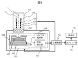
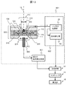
- FIG. 3 shows a configuration diagram of the scanning electron microscope according to the second embodiment.
- the housing 10 includes a column in which an electron optical system that irradiates an electron beam to a sample to be observed is built in, and a sample chamber in which the sample is placed.
- the electron optical system is arranged in a column and focuses the electron gun 11 and the electron beam 12 emitted from the electron gun 11 and irradiates the sample 200 as a minute spot onto the sample lens 200, the objective lens 62, and the astigmatism of the electron beam 12.
- a stage 64 that can move three-dimensionally is provided in the sample chamber.
- the sample 200 is held in the sample chamber 100, and the sample chamber 100 is connected to a signal detection circuit and constitutes a detector 101.
- the sample chamber 100 is mounted on the stage 64 via an insulator spacer 65. As a result, the sample chamber 100 is placed on the stage 64 while being electrically insulated from the stage 64.
- the electron optical system and the stage 64 are controlled by the main controller 14.
- the detection signal (voltage signal) from the detector 101 is input to the main control unit 14.
- the voltage signal output from the signal detection unit 50 of the detector 101 for each irradiation position of the electron beam 12 onto the sample chamber 100 is converted into pixel gradation data according to its intensity. And is output to the computer 15 as image data each time one frame scan is completed, one line scan is completed, or one pixel scan is completed depending on the deflection speed.
- the image data is displayed on the display unit 16 by the computer 15.
- the configuration of the detector 101 will be described with reference to the configuration diagram of the detector 101 shown in FIG. 4A.
- the sample chamber 100 (the cross-sectional view of which is shown in the figure) is a stack of several mm to several tens of mm square.
- the sample chamber 100 includes a diaphragm that isolates the sample 200 from the vacuum inside the sample chamber on the side of the irradiation surface of the electron beam 12.
- the diaphragm has at least two layers of the first insulating layer 110 on the sample 200 side and the conductive layer 120 on the side on which the electron beam 12 is incident.
- the first insulating layer 110 is supported by the outer frame portion 130 provided for the purpose of maintaining strength, and the conductive layer 120 is uniformly formed on the outer frame portion 130 and the first insulating layer 110.
- the sample 200 is held between the diaphragm and the sample holding layer facing the diaphragm.
- the sample holding layer has at least two layers of the second insulating layer 111 and the substrate 131 supporting the second insulating layer 111 on the sample 200 side.
- the second insulating layer 111 is provided to prevent corrosion of the substrate 131 by the sample 200.
- an intermediate layer 115 is provided to form a holding space for the sample 200 by providing a predetermined gap between the diaphragm (first insulating layer 110) and the sample holding layer (second insulating layer 111). There is.
- the intermediate layer 115 also plays a role of isolating the sample 200 from the vacuum in the sample chamber.
- the reference potential portion 140 is provided in contact with the sample holding layer (substrate 131). As will be described later, the potential of the reference potential portion 140 is the reference potential when the potential is applied to the conductive layer 120. As will be described later, the potential applied to the conductive layer 120 is supplied by the bias power supply unit 20.
- a silicon nitride (SiN) film can be used for the first insulating layer 110, a metal thin film such as tungsten or tantalum can be used for the conductive layer 120, and a silicon (Si) substrate can be used for the outer frame portion 130.
- a silicon nitride (SiN) film or a silicon oxide (SiO 2 ) film can be used as the second insulating layer 111, and a silicon substrate can be used as the substrate.
- an insulating film such as a silicon oxide (SiO 2 ) film can be used for the intermediate layer 115, and a metal layer such as aluminum or copper can be used for the reference potential portion 140.
- the stacked body forming the sample chamber 100 can be formed using a semiconductor process (MEMS process). Due to the detection principle of the detector described later, both the first insulating layer 110 and the conductive layer 120 have a uniform thickness and do not have a concavo-convex structure on the surface (more specifically, the surface when observed with a scanning electron microscope). Unevenness that does not show the contrast of unevenness is allowed, and the size of the unevenness on the surface at this time is preferably about 10 nm or less). This can be realized by using a semiconductor process for forming the laminated body and, for example, forming a metal thin film for forming the conductive layer 120 by sputtering film formation.
- MEMS process semiconductor process
- the intermediate layer 115 does not have to have a physical structure.
- the sample chamber 100 is arranged in a box-shaped vacuum partition as shown in FIG. 4B.
- the vacuum partition is composed of a vacuum partition lower part 520 and a vacuum partition upper part 521.
- the vacuum partition lower part 520 is an insulator such as acrylic, and the vacuum partition upper part 521 is a conductor such as aluminum.
- the lower part 520 of the vacuum partition and the upper part 521 of the vacuum partition are connected via a sealing material 523 for airtightness, and the space around the sample 200 is maintained at atmospheric pressure or at a vacuum degree lower than that of the sample chamber. In this case, the gap between the first insulating layer 110 and the second insulating layer 111 is held by the sandwiched sample 200.
- an opening 501 for passing an electron beam is provided on the upper surface of the vacuum partition upper part 521.
- the vacuum partition upper component 521 is electrically connected to the conductive layer 120, and a current signal is detected from the vacuum partition upper component 521.
- the vacuum partition lower part 520 is provided with a connector 524 for taking out a conducting wire 525 for keeping the reference potential part 140 at a predetermined potential.
- the detection principle of the detector 101 will be described with reference to FIG. 4A.
- the electron beam 12 is scattered in the conductive layer 120 and the first insulating layer 110.
- carriers (insulating layer-originating carriers) 300 are generated.
- the generation principle of the insulating layer origin carrier 300 will be described later with reference to FIG.
- the amount of the insulating layer-originating carriers 300 generated depends on the electric field strength generated in the first insulating layer 110 and the sample 200 immediately below the first insulating layer 110.
- the insulating layer origin carrier 300 flows into the bias power supply unit 20 through the conductive layer 120.
- signal electrons 301 such as SE and BSE are emitted from the electron beam scattering region 17 of the conductive layer 120 into the vacuum.
- carriers (conductive layer origin carriers) 302 corresponding to the balance of the number of incident electron beams 12 and the number of generated signal electrons 301 are generated.
- N the number of signal electrons N is generated with respect to the number of electrons 1 of the electron beam 12
- N ⁇ 1 conductive layer origin carriers 302 are generated.
- N is larger than 1
- the polarity of the conductive layer-originating carrier 302 is positive as shown in FIG. 4A.
- the conductive layer origin carrier 302 also flows into the bias power supply unit 20.
- the signal detection unit 50 detects carriers that have flowed into the bias power supply unit 20 and outputs a voltage signal according to the amount of carriers to the main control unit 14.
- the amount of the insulating layer-originating carrier 300 generated changes depending on the sample 200.
- the amount of carriers 302 originating from the conductive layer is constant. This is because, as described above, the conductive layer 120 has a uniform structure with no unevenness on the surface, so that the amount of signal electrons 301 generated is constant.
- the spread of the electron beam scattering region 17 due to the electron beam 12 depends on the acceleration voltage of the electron beam 12.
- the acceleration voltage of the electron beam 12 is preferably set to a low acceleration voltage that does not substantially penetrate the first insulating layer 110 in the internal region 310.
- a bias voltage is applied to the conductive layer 120 by the bias power source section 20 and the reference potential section 140 is grounded.
- the potentials of the bias power supply section 20 and the reference potential section 140 may be set so that a desired electric field strength is generated in the first insulating layer 110 and the sample 200 directly below the first insulating layer 110.
- the bias power supply unit 20 may be set to the ground potential
- the reference potential unit 140 may be applied with a voltage having a polarity opposite to that of the bias voltage in the example of FIG. 4A.
- the bias voltage and the voltage applied to the reference potential portion may be determined so that a predetermined voltage is generated between the conductive layer 120 and the reference potential portion 140 with a certain potential of the system as the ground potential.
- the insulating layer origin carrier 300 is not generated. This is because the electron beam 12 does not pass through the outer frame portion 130 and does not reach the first insulating layer 110.
- the conductive layer origin carrier 302 changes depending on the structure of the outer frame part 130. This is because, as is well known, the amounts of SE and BSE that are signal electrons are changed by reflecting the three-dimensional structure of the irradiated body. That is, when the scanning range of the electron beam 12 is in the outer frame region 311, only the carrier 302 originating from the conductive layer flows into the bias power supply unit 20, and the signal detection unit 50 detects the carriers flowing into the bias power supply unit 20.
- the voltage signal according to the amount of carriers is output to the main control unit 14.
- the contrast depending on the three-dimensional structure of the irradiated body appears in the image data, and an image equivalent to the absorption current image in SEM can be obtained.
- the scanning range of the electron beam 12 is a signal originating from the sample 200 in the inner region 310 of the sample chamber 100, and the scanning range of the electron beam 12 is outside in the outer frame region 311 of the sample chamber 100.
- a signal originating from the three-dimensional structure of the frame 130 can be acquired. Therefore, the electron beam 12 for irradiating the sample chamber 100 is optimized by performing focus adjustment and astigmatism correction of the electron beam 12 using the three-dimensional structure of the outer frame 130, and the sample 200 is observed by the optimized electron beam 12.
- Focus adjustment and astigmatism correction of the electron beam 12 can be performed using an SE detector or a BSE detector included in the scanning electron microscope. In this case, the detector is adjusted by adjusting the electron beam 12 and observing the sample. Must be switched.
- the electron beam can be adjusted and the sample can be observed without switching the detector, so that the convenience is improved and the observation throughput is improved.
- FIG. 5 shows the top shape (portion) of the sample chamber 100.
- the upper stage is a top view of the sample chamber 100
- the lower stage is a sectional view.
- the cross-sectional view in the lower row corresponds to the cross-sectional shape of the one-dot chain line portion indicated by AA in the top view.
- the outer frame portion 130 has a window portion 313 that is recessed in an inverted pyramid shape, and the inner region 310 that is the bottom surface of the window portion 313 has a rectangular shape.
- rectangular areas including the internal area 310 and the inclined surface in contact with the internal area 310 are referred to as outer frame edge portions 314 to 317.
- it is assumed that the sample is not enclosed in the sample chamber 100 and the sample holding space is in a vacuum.
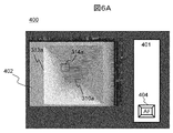
- FIG. 6A and 6B show an example of the display screen 400 displayed on the display 16.
- the display screen 400 includes an optical condition such as an accelerating voltage and an observation magnification, a condition display unit 401 indicating position information of an observation place, an SEM image display unit 402, and an autofocus button 404 described later.
- FIG. 6A is a display screen when the entire inverted pyramid-shaped window 313 of the outer frame 130 is in the field of view. An image 313a of the inverted pyramid-shaped window portion 313 and an image 310a of the internal region 310 are observed in the central portion.
- FIG. 6B is a display screen when an image 314a of one outer frame edge portion 314 of the inverted pyramid-shaped window portion 313 shown in FIG. 6A is enlarged and observed.
- the SEM image based on the voltage signal of the detector 101 detects the same signal electron-derived information as the detection target of the scanning electron microscope as the absorption current, and thus the outer frame portion 130
- the structure specifically the inverted pyramid shape, appears as contrast.
- the internal region 310 in this example, since the sample does not exist under the first insulating layer 110, no contrast appears.
- the internal region of the SEM images of FIGS. A contrast reflecting the sample 200 appears in the image 310a of 310.
- the user sets the conditions on the GUI or the operation tool at the user's hand (not shown). Specifically, first, as shown in FIG. 6A, the field of view and the observation magnification are set so that the entire inverted pyramid-shaped window 313 is in the field of view, and the focus condition is set so that an SEM image with high sharpness can be obtained at the observation magnification. Adjust astigmatism correction.
- the main controller 14 controls each part of the device according to the conditions set by the user. Specifically, when setting the observation magnification, the main control unit 14 controls the deflector 13 so that the electron beam 12 scans the observation magnification region desired by the user.
- the main control unit 14 controls the stage 64 or the image shifter 63 to move the observation visual field two-dimensionally so that the visual field desired by the user can be obtained.
- the main controller 14 controls the objective lens 62 and the astigmatism corrector 61, respectively, and adjusts the focusing state of the electron beam 12 so as to obtain the sharpness desired by the user. To do.
- the user After adjusting the focus condition and the astigmatism correction described above, the user sets a desired observation magnification and a desired field of view on the GUI or an operation tool at the user's hand (not shown), observes the internal region 310, and the target. An SEM image of the sample is obtained.
- the observation SEM image of the outer frame edge portion 314 as shown in FIG. 6B is used at the desired observation magnification.
- the procedure may be performed and each condition may be set so that the sharpness desired by the user is obtained.
- FIG. 7 shows an example of a flowchart of the autofocus function.
- the user decides the desired field of view and the observation magnification, and starts the autofocus process by pressing the autofocus button 404 (see FIGS. 6A and 6B) on the GUI or operating the operation tool at the user's hand (not shown).
- step S1 the computer 15 substitutes 0 for the number of trials N.
- step S2 the main controller 14 controls the deflector 13, the image shifter 63, and the stage 64 to acquire a low-magnification image as shown in FIG. 6A.
- step S3 the computer 15 performs image processing on the low-magnification image, determines the locations of the four outer frame edge portions 314 to 317 (see FIG. 5), and stores the coordinates.
- step S4 the main control unit 14 controls the image shifter 63 and the stage 64 to move the visual field so that the visual field center becomes the center of any of the four outer frame edge portions 314 to 317.
- the outer frame edge portion to be selected as the destination it is preferable to select the outer frame edge portion closest to the target observation target site.
- step S5 the main control unit 14 controls the deflector 13 to acquire a high-magnification image as shown in FIG. 6B at a desired observation magnification.
- step S6 the computer 15 performs image processing on the high-magnification image and calculates a sharpness evaluation value.
- step S7 the computer 15 compares the sharpness evaluation value with a threshold value stored in advance and determines success or failure. Specifically, the computer 15 makes a failure determination if the sharpness evaluation value exceeds the threshold value, adds 1 to the number of trials (step S10), and compares the number of trials N with a prestored number of trials upper limit. (Step S11). If the number of trials N is less than the upper limit of the number of trials, the main controller 14 controls the objective lens 62 and the astigmatism corrector 61 to change the focusing state of the electron beam 12 (step S12), and again to step S5. Process from.
- step S13 if the number of trials N is equal to or more than the upper limit of the number of trials, error processing is performed and the processing ends (step S13).
- the main control unit 14 controls the objective lens 62 and the astigmatism corrector 61 to return the focusing state of the electron beam 12 to the condition before the start of the autofocus processing, and the computer 15 displays The user is notified that the autofocus processing has failed on the copy screen 400.
- step S7 the computer 15 determines success if the sharpness evaluation value is less than or equal to the threshold value, and proceeds to step S8.
- step S8 the main control unit 14 controls the deflector 13, the image shifter 63, and the stage 64 so that the observation magnification and the observation visual field desired by the user are obtained.
- step S9 the main control unit 14 captures an image of a desired field of view at a desired magnification, the computer 15 displays the image information on the display unit screen 400, stores it in the internal storage, and ends the process.
- the focus adjustment and the astigmatism can be easily performed based on the detection signal from the detector 101 without switching to another detector image such as the SE detector of the scanning electron microscope. Aberration correction can be performed.
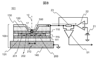
- the bias power supply unit 20 (see FIG. 4A) is configured by the constant voltage source 21 and the voltage follower circuit 22, and the signal detection unit 50 is configured by the resistor 23 and the amplifier 51.
- the constant voltage source 21 is connected to the positive input terminal of the voltage follower circuit 22, and the conductive layer 120 of the sample chamber 100 is connected to the negative input terminal of the voltage follower circuit 22.
- the output terminal of the voltage follower circuit 22 and the conductive layer 120 of the sample chamber 100 are connected via the resistor 23, and the potential difference between both ends of the resistor 23 is amplified by the amplifier 51 and output as a voltage signal.
- the sample 200 is, for example, water 201 in which cells 202 that can be regarded as a protein complex are dispersed. Since the permittivity of water is about 80, whereas the permittivity of protein is 2 to 3, the potential gradient of the water portion, that is, the electric field strength becomes gentle as compared with the electric field strength of the cell portion.
- the electric field strength inside the cells is high, and therefore the electric field strength inside the first insulating layer 110 directly above the interface is high. It becomes relatively low.
- the electric field strength in the first insulating layer 110 immediately above the interface in that region is relatively high.
- the two-dimensional electric field strength distribution inside the first insulating layer 110 along the interface between the first insulating layer 110 and the inside of the sample 200 in the internal region 310 reflects the distribution of the dielectric constant near the interface. It will be what you did.
- the electron beam 12 When the electron beam 12 is set to an accelerating voltage that does not substantially pass through the first insulating layer 110, the electron beam 12 does not reach the sample 200, but the electron beam scattering region 17 spreads in the first insulating layer 110. , And scattering of primary electrons having energy in that range occurs.
- the primary electrons scattered in the first insulating layer 110 impart energy with about three times the work function of the material of the first insulating layer 110, one electron-hole pair is generated.
- the first insulating layer 110 is a silicon nitride film
- its work function is about 3 eV, and therefore, a pair of electron-hole pairs are generated by applying energy of about 9 eV from the scattered primary electrons.
- the depth of the electron beam scattering region 17 of the incident electron beam 12 is uniform regardless of the scanning region, and the electron beam scattering region 17 has a uniform depth.
- the energy distribution of the primary electrons is uniform regardless of the scanning area. Therefore, the number of electron-hole pairs generated in the first insulating layer 110 is uniform regardless of the scanning region.
- the rate at which the generated electron-hole pairs are separated as carriers without recombination is determined by the two-dimensional electric field inside the first insulating layer 110 along the interface between the first insulating layer 110 and the sample 200.
- the amount of the insulating layer-originating carrier 300 detected at each irradiation position of the electron beam 12 onto the sample chamber 100 reflects the distribution of the dielectric constant in the sample 200. This is the principle of contrast generation of the sample to be observed in the scanning electron microscope according to this embodiment.
- the same negative voltage is applied to the conductive layer 120 as well, so that the electron-hole pairs generated as shown in FIG.
- the positive charges at are separated on the conductive layer 120 side and flow into the voltage follower circuit 22. Since the input impedance of the negative input terminal of the voltage follower circuit 22 is much higher than the output, the carriers that have flowed in via the conductive layer 120 will flow through the resistor 23. At this time, a potential difference according to the amount of carriers is generated at both ends of the resistor 23, and the potential difference can be detected by the amplifier 51.
- a specific form of the amplifier 51 may be an instrumentation amplifier.
- the electric field 12 is charged by the electron beam 12 generated in the first insulating layer 110 as described above. Since the charge of the electrons is negative, the charging potential becomes negative with respect to the reference potential part 140. Therefore, also in this case, when the output of the constant voltage source 21 is negative with respect to the potential of the reference potential part 140. A signal with the same polarity as is obtained.
- the potential of the conductive layer 120 becomes equal to the output of the constant voltage source 21 by the connection of the voltage follower circuit 22 shown in FIG. It is possible to maintain. That is, the potential difference between the conductive layer 120 and the reference potential portion 140 can be maintained constant regardless of the amount of electron-hole pairs generated in the first insulating layer 110. However, in actual use, the potential difference across the resistor 23 depending on the amount of carriers is sufficiently smaller than the voltage across the constant voltage source 21, and the resistor 23 is outside the negative feedback of the voltage follower circuit 22.
- the signal detection circuit shown in FIG. 8 is suitable for sample observation at a high frame rate because an amplifier can be connected to the conductive layer 120 directly above the carrier generation source to reduce the signal path impedance. Moreover, the impedance of the signal path until the electron-hole pairs generated in the electron beam scattering region 17 are separated by the electric field applied to the first insulating layer 110 and flow into the voltage follower circuit 22 as carriers becomes the sample 200. Do not depend. Therefore, even if the content of the sample 200 is changed, it is not necessary to newly search for the scanning speed of the electron beam 12 suitable for the sample, and observation with high throughput is realized using an image with a high frame rate. It becomes possible.
- the observation magnification is set so that the shape and material of the sample can be visually recognized on the observation image, that is, at least several pixels or more.
- the response frequency band of the signal detection circuit necessary for displaying a sample shape of several pixels or more with high image quality under a display condition of an image size of 640 pixels ⁇ 480 pixels and a frame rate of 12 fps is about 700 kHz. .
- FIG. 9 shows a circuit simulation result of the response frequency characteristic of the signal detection circuit of this example when the current-voltage conversion rate was set to 10 9 [V / A].
- the graph of FIG. 9 is standardized so that the current-voltage conversion rate of 10 9 [V / A] is 0 dB.
- the high cutoff frequency of the signal detection circuit is about 1.4 MHz, which exceeds the response frequency band of the detection circuit required for visualization of a series of images described above, that is, about 700 kHz (one-dot chain line in FIG. 9) required for moving image observation. . This makes it possible not only to acquire a still image of the sample, but also to acquire motion and morphological changes unique to a living biological sample as a moving image.
- the signal detection circuit can be realized not only in the example of FIG. 8 but also in another configuration.
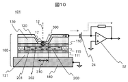
- the bias power supply unit 20 (see FIG. 4A) is configured by the constant voltage source 24, and the signal detection unit 50 is configured by the transimpedance amplifier 52.
- An easy form of the constant voltage source 24 is a battery. The return current corresponding to the carrier generated as described above and flowing into the constant voltage source 24 through the conductive layer 120 flows through the transimpedance amplifier 52, and thus the voltage signal corresponding to the amount of carriers is detected. Is possible.
- the bias power supply unit 20 (see FIG. 4A) is configured by the constant voltage source 24, and the signal detection unit 50 is configured by the resistor 25 and the voltage amplifier 53.
- the constant voltage source 24 has one terminal connected to the conductive layer 120 and the other terminal connected to one terminal of the voltage amplifier 53.
- the resistor 25 is connected between the other terminal of the constant voltage source 24 and the reference potential part.
- the return current corresponding to the carrier generated as described above and flowing into the constant voltage source 24 via the conductive layer 120 flows through the resistor 25, and the voltage amplifier 53 amplifies the potential difference across the resistor 25, It is possible to detect a voltage signal according to the amount of carriers.
- the potential of the conductive layer 120 in the example of FIG. 11 varies by the potential difference between both ends of the resistor 25, but in actual use, the amount of variation is sufficiently smaller than the voltage across the constant voltage source 24, and the conductive layer
- the potential of 120 can be considered constant.
- the sample holding layer includes a second insulating layer 111 on the sample 200 side and a second outer frame portion 911 that supports the second insulating layer 111.
- a window portion 912 is provided in the second outer frame portion 911, and the second insulating layer 111 is exposed to the outside atmosphere in the second inner region 913 corresponding to the bottom portion of the window portion 912.
- the second inner region 913 is preferably formed in the same region as the first inner region 310 or in a region covering the first inner region 310 when viewed from the upper surface of the sample chamber 900.
- a silicon nitride (SiN) film can be used as the material of the second insulating layer 111, and a silicon (Si) substrate can be used as the material of the second outer frame portion 911.
- a reference potential portion 910 that gives a reference potential to the conductive layer 120 has a rod shape and is arranged close to the second internal region 913. With such a configuration, the distance between the conductive layer 120 and the reference potential portion 910 can be reduced, so that the electric field strength can be increased compared to the configuration of the second embodiment even when the same potential is applied to the conductive layer 120. It will be possible.
- the sample chamber 900 is arranged in a box-shaped vacuum partition similar to that shown in FIG. 4B, and the space around the sample chamber 900 is maintained at atmospheric pressure or at a vacuum degree lower than that of the sample chamber. You may In this case, the configuration is the same as that of the fourth embodiment (FIG. 14), and the detection electrode 820 of the fourth embodiment may be read as the reference potential portion 910.
- the sample holding layer includes the second insulating layer 111 and the second outer frame portion 810 supporting the second insulating layer 111 on the sample 200 side, as in the third embodiment.
- a window portion 811 is provided in the second outer frame portion 810, and the second insulating layer 111 is exposed to the outside atmosphere in the second inner region 812 corresponding to the bottom portion of the window portion 811.
- the second inner region 812 is preferably formed in a region that is the same as the first inner region 310 or covers the first inner region 310 when viewed from the upper surface of the sample chamber 800.
- a silicon nitride (SiN) film can be used as the material of the second insulating layer 111, and a silicon (Si) substrate can be used as the material of the second outer frame portion 810.
- a detection electrode 820 is provided in the vicinity of the second internal region 812, and the detection electrode originates from the insulating layer origin carrier 300.
- a second signal detection circuit 821 for detecting an electric signal generated in 820 is included.
- the detection electrode 820 plays the role of a reference potential section that gives a reference potential to the conductive layer 120 in the configuration of the detector of FIG. 4A.
- the sample chamber 800 is mounted on the stage 64 with the detection electrode 820 and the second outer frame portion 810 electrically insulated from the stage 64. Specifically, as shown in FIG. 3, it is mounted on the stage 64 via an insulator spacer 65.
- the detection electrode 820 is connected to the second signal detection circuit 821, and the second signal detection circuit 821 outputs the electric signal detected by the detection electrode 820 to the main control unit 14 as a voltage signal according to its strength.
- the main control unit 14 converts the voltage signal output from the second signal detection circuit 821 for each deflection position of the electron beam 12 onto the sample chamber 800 into pixel gradation data according to the intensity, and the deflection speed.
- the image data is output to the computer 15 every time one frame scanning is completed, one line scanning is completed, or one pixel scanning is completed.
- the image data is displayed on the display unit 16 by the computer 15. With such a configuration, it is possible to simultaneously acquire two types of image data based on the signal obtained from the first signal detection circuit 802 and the signal obtained from the second signal detection circuit 821.
- the outside atmosphere of the sample chamber 800 may be the same vacuum atmosphere as the sample chamber.
- the sample chamber 800 may be arranged in a box-shaped vacuum partition similar to that shown in FIG. 4B, and the space around the sample chamber 800 may be maintained at atmospheric pressure or at a vacuum degree lower than that of the sample chamber.
- the state is shown in FIG.
- the vacuum partition is composed of a vacuum partition lower part 920 and a vacuum partition upper part 921.
- the vacuum partition lower part 920 is an insulator such as acrylic
- the vacuum partition upper part 921 is a conductor such as aluminum.
- the vacuum partition lower part 920 and the vacuum partition upper part 921 are connected via a sealing material 923 for airtightness, and maintain the space around the sample 200 at atmospheric pressure or at a vacuum degree lower than that of the sample chamber.
- the upper part 921 of the vacuum partition is electrically connected to the conductive layer 120, and an electric signal is detected from the upper part 921 of the vacuum partition.
- the detection electrode 820 is fixed to the vacuum partition lower part 920 so as to be close to the second internal region 812 of the sample chamber 800.
- two types of images based on the signal from the first signal detection circuit 802 and the signal from the second signal detection circuit 821 can be simultaneously acquired and compared. For example, when a specific contrast different from the image obtained by the second signal detection circuit 821 occurs at a specific portion of the image obtained by the first signal detection circuit 802, foreign matter is present on the vacuum side surface of the conductive layer 120. Is likely to.
- the signal obtained by the first signal detection circuit 802 is both the signal electron origin information (conductive layer origin carrier) and the information originating in the sample 200 ( (Insulating layer origin carrier), whereas the signal obtained by the second signal detection circuit 821 does not include information of signal electron origin, but only information of sample 200 origin. Therefore, for example, when minute metal particles are present as foreign matter on the vacuum side surface of the conductive layer 120, more signal electrons (mainly SE) are generated around the metal particles than on other surfaces. For this reason, the voltage signal detected by the first signal detection circuit 802 in the portion where the metal particles are present increases as the number of carriers 302 originating in the conductive layer increases.
- the presence of the metal particles causes the electron beam 12 to lose energy, and the probability of reaching the first insulating layer 110 around the metal particles decreases. For this reason, the number of insulating layer-originating carriers 300 generated in the first insulating layer 110 is reduced as compared with the surroundings. As a result, the voltage signal detected by the second signal detection circuit 821 in the portion where the metal particles are present becomes small due to the phenomenon of the insulating layer origin carrier 300. In this way, when there is a difference between the obtained two types of images, it can be determined that foreign matter is highly likely to be present on the vacuum side surface of the conductive layer 120 at the portion where the difference occurs.
- Reference numeral 10 housing, 11: electron gun, 12: electron beam, 13: deflector, 14: main control unit, 15: computer, 16: display unit, 17: electron beam scattering region, 20: bias power supply unit, 21: Constant voltage source, 22: voltage follower circuit, 23: resistor, 24: constant voltage source, 25: resistor, 50: signal detector, 51: amplifier, 52: transimpedance amplifier, 53: voltage amplifier, 60: capacitor Lens, 61: Astigmatism corrector, 62: Objective lens, 63: Image shifter, 64: Stage, 65: Insulator spacer, 100, 800, 900: Sample chamber, 101, 602, 801, 901: Detector , 110: first insulating layer, 111: second insulating layer, 115: intermediate layer, 120, 604: conductive layer, 130, 605, 810, 911: outer frame part, 131: substrate, 140.
Landscapes
- Chemical & Material Sciences (AREA)
- Analytical Chemistry (AREA)
- Analysing Materials By The Use Of Radiation (AREA)
Abstract
簡便かつ高い観察スループットで、染色処理や固定化処理なしに生物化学試料を非侵襲で観察することを可能とする荷電粒子線装置及び検出器を提供する。電子光学系と、ステージ(64)と、試料(200)を保持し、試料(200)に接する第1の絶縁層(110)と、第1の絶縁層(110)上に形成される導電層(120)とを有する試料チャンバ(100)と、導電層(120)に接続され、導電層(120)に流れる電流を検出する信号検出回路(20),(50)と、電子光学系とステージ(64)とを制御する主制御部(14)とを有し、主制御部(14)は、電子光学系からステージ(64)に載置された試料チャンバ(100)の導電層(120)に電子線(12)を照射し、信号検出回路(20),(50)からの検出信号が入力される。
Description
本発明は、荷電粒子線を照射して発生する検出信号を利用し、試料の形状または材質等を観察する荷電粒子線装置及び検出器に関する。より詳細には、生物化学試料や液体試料を、状態の変化やダメージを抑え、非侵襲の状態で観察することが可能な荷電粒子線装置及び検出器に関する。
荷電粒子線装置の一つである走査電子顕微鏡(SEM:Scanning Electron Microscope)は、金属やセラミックスなどの材料試料だけでなく、生物試料を高分解能で観察するツールとしても広く用いられている。
一般的に、これらの装置では筐体を真空排気し、試料を真空雰囲気中に配置して試料を撮像する。電子線は、大気などのガス分子や液体分子によって散乱されるため、電子線の通過経路は真空雰囲気に保つことが好ましい。一方、真空雰囲気中に置かれると、生物化学試料や液体試料はダメージを受け、または、状態が変化してしまうため、非侵襲の状態での観察は困難であるとされてきた。しかしながら、このような試料に対する非侵襲観察ニーズは大きく、近年、観察対象試料を、大気圧環境下や液中環境化で観察可能な電子顕微鏡が開発されている。
特許文献1には、試料を大気圧雰囲気下に保った状態で観察可能なSEMが記載されている。この装置では、電子光学系と試料の間に電子線が透過可能な隔膜を設けて真空状態と大気状態とを仕切る。隔膜の大気側近傍に試料を配置して、基本的に試料と隔膜とが非接触の状態で電子線を試料に直接当て、試料から発生する信号電子を検出することでSEM像を得る。この装置では、真空隔壁として働く隔膜によって電子線が隔膜に到達する直前までの経路を高真空状態に維持することで電子線の散乱を防ぎ、かつ電子線の散乱が生じる隔膜透過後の領域を隔膜から試料の間の非常に短い距離に限定することで観察が可能となっている。
また、特許文献2、3には染色処理や固定化処理を施すことなく、走査電子顕微鏡を用いて水溶液中の生物試料を生きたままの状態で観察するための試料ホルダ、観察システムが開示されている。走査電子顕微鏡で生物試料を観察する場合、電子線と生物試料との相互作用が極めて低いため、観察画像のコントラストを向上させるために、様々な染色処理や固定化処理を施すことが一般的であった。このような処理を施すと、観察対象である生物試料は死滅してしまい、生きている状態での観察はできなくなる。また、高エネルギーの電子線を直接試料に当てる場合、そのダメージによって生物試料が破壊される場合がある。
特許文献2、3開示の観察システムでは、一方主面が観察試料の保持面である第1の絶縁性膜と、第1の絶縁性膜の他方主面に積層された導電性膜を備えた液中試料ホルダを用い、導電性膜をグランド電位もしくは所定のバイアス電圧を印加した状態で導電性膜側から電子線を照射する。照射された電子線に起因して、第1の絶縁性膜の一方主面には局所的な電位変化が生じる。この電位変化に基づく信号を、観察試料を挟んで反対側に配置された第2の絶縁性膜の下方に設けた検出電極により検出する。第1の絶縁性膜に生じた電位変化に基づく信号は、観察試料を伝搬し、検出電極により検出される。このときの信号の伝搬力には観察試料に応じて違いがある。例えば、水は比誘電率が約80と高いため、信号を良く伝搬させる一方、生物試料は比誘電率が2~3程度と低く、信号の伝搬力が低下する。このため、観察試料を伝搬した電位変化信号の強度差に基づき、水溶液中の生物試料を染色処理なしに、高いコントラストで観察することが可能となる。この手法は、高エネルギーの電子線を直接観察対象試料に当てる必要がないため、液中生物試料のダメージレス観察に適している。
特許文献1の装置では、信号電子を検出するための構成物として検出器が必要となる。このため、コストの上昇につながるおそれもある。
特許文献2、3の観察システムでは、電位変化信号の検出に、試料ホルダの下方に設けた検出電極を用いる。観察の原理からは、試料ホルダは、電子線照射する側に第1の絶縁性膜と導電性膜の積層膜が、観察試料を挟んで対向する面に第2の絶縁性膜があればよいが、試料ホルダとして用いるためには、試料ホルダの強度を維持するフレームとなる層を設け、このフレームとなる層を部分的に加工して、所望の積層膜を形成したり、第2の絶縁性膜を露出させたりする必要がある。特に、電位変化信号の検出のために試料ホルダの下方に設けた検出電極を用いているために、試料ホルダの上面、下面ともに加工が必要であり、コストの上昇につながるおそれもある。
本発明はこのような問題に鑑みてなされたものであり、その目的とするところは、簡便かつ高い観察スループットで、染色処理や固定化処理なしに生物化学試料や液体試料を状態の変化やダメージを抑え、非侵襲の状態で観察することを可能とする荷電粒子線装置及び検出器を提供することにある。
本発明の一実施態様である荷電粒子線装置は、電子光学系と、ステージと、試料を保持し、試料に接する第1の絶縁層と、第1の絶縁層上に形成される導電層とを有する試料チャンバと、導電層に接続され、導電層に流れる電流を検出する信号検出回路と、電子光学系とステージとを制御する主制御部とを有し、主制御部は、電子光学系からステージに載置された試料チャンバの導電層に電子線を照射し、信号検出回路からの検出信号が入力される。
荷電粒子線装置により、染色処理や固定化処理なしに生物化学試料や液体試料を、状態の変化やダメージを抑え、非侵襲の状態で観察することが可能となる。
その他の課題と新規な特徴は、本明細書の記述および添付図面から明らかになるであろう。
以下、本発明の実施の形態を、図面を用いて説明する。
図1に実施例1にかかる走査電子顕微鏡の構成図を示す。カラム610には、観察対象である試料に対して電子線を照射する電子光学系が内蔵される。電子光学系はカラム610に配置され、電子銃11と、電子銃11から放出された電子線12を集束し、微小スポットとして試料200に照射するコンデンサレンズ60及び対物レンズ62、電子線12の非点収差を補正する非点収差補正器61、電子線12を試料200上で2次元的に走査する偏向器13、電子線12の走査中心位置を試料200上で2次元的にシフトさせるイメージシフト器63を含む。カラム610は高真空環境に保たれる。
また、試料200を格納する試料室600を備え、試料室600には、3次元的に移動可能なステージ64が設けられる。試料室600は、一例としては大気圧雰囲気のような、カラム610の真空度より低い真空度の雰囲気中に保たれる。試料200は試料室600内のステージ64に保持されている。
カラム610と試料室600とは、真空隔膜ホルダ601を介して接続されており、真空隔膜ホルダ601は信号検出回路と接続され、検出器602を構成している。
電子光学系及びステージ64は主制御部14によって制御されるとともに、主制御部14には検出器602からの検出信号(電圧信号)が入力される。
検出器602の構成については後述するが、試料200上への電子線12の照射位置ごとに検出器602の信号検出部50から出力された電圧信号を、その強度に応じた画素階調データに変換し、偏向速度によって1フレーム走査の完了ごと、あるいは1ライン走査の完了ごと、あるいは1画素走査の完了ごとに画像データとしてコンピュータ15に出力する。画像データはコンピュータ15によって表示部16に表示される。
図2に示す検出器602の構成図を用いて、検出器602の構成について説明する。真空隔膜ホルダ601(図ではその断面図を示している)は数mm~十数mm角の積層体である。真空隔膜ホルダ601は、電子線12の照射面側にカラム内真空から試料200が配置される低真空あるいは大気圧雰囲気を隔離する隔膜を備えている。隔膜は試料200側に絶縁層603、電子線12が入射する側に導電層604の少なくとも2層を有している。絶縁層603は強度維持の目的で設けられている外枠部605によって支持され、導電層604は、外枠部605及び絶縁層603上に均一に形成されている。試料200は、試料室600内のステージ64上に載置される。
各層の材料について例示する。絶縁層603は窒化シリコン(SiN)膜を、導電層604はタングステン、タンタルなどの金属薄膜を、外枠部605はシリコン(Si)基板を用いることができる。真空隔膜ホルダ601を構成する積層体は半導体プロセス(MEMSプロセス)を用いて形成することができる。絶縁層603及び導電層604は双方ともに厚みが均一で、表面に凹凸構造を持たない(より具体的には、走査電子顕微鏡で観察した場合に表面の凹凸のコントラストが表れない程度の凹凸は許容され、このときの表面の凹凸の大きさはおよそ10nm以下)ことが好ましい。これは、積層体の形成に半導体プロセスを用い、例えば、導電層604を形成する金属薄膜をスパッタ製膜により形成することで実現できる。
次に、図2を用いて検出器602の検出原理を説明する。電子線12は、真空隔膜ホルダ601に照射されると導電層604及び絶縁層603を貫通し試料200上に到達する。試料200からは、SE(二次電子:Secondary Electron)やBSE(後方散乱電子:Back-Scattered Electron)をはじめとする信号電子が放出される。
このうち、最大値では電子線12と同等のエネルギーをもつBSE606は、絶縁層603及び導電層604を貫通し、カラム構造物607に当たる。一例としては、カラム構造物607は対物レンズの一部であっても良い。カラム構造物607からは、SE608が発生する。実施例1においては、導電層604には、カラム構造物607の電位に対して正の電圧が、バイアス電源部20によって印加されている。この電位差によって、負の電荷を持つSE608は、導電層604に向かって加速され、導電層604で吸収されることによりバイアス電源部20に流入する。
信号検出部50はバイアス電源部20に流入した電流を検出し、電流の量に応じた電圧信号を主制御部14に出力する。SE608の発生量および検出される電流量はBSE606の発生量に対応して変化するため、試料のBSE像を得ることができる。
電子線12による真空隔膜(絶縁層603及び導電層604)の透過能はその加速電圧に依存する。以上の検出原理より、実施例1においては、電子線12の加速電圧は、絶縁層603及び導電層604を透過する高加速電圧に設定されることが好ましい。
信号検出回路を構成するバイアス電源部20及び信号検出部50の詳細な構成例は同様に構成可能な実施例2において説明する。また、実施例1の構成においても真空隔膜ホルダ601に電子線12が照射されることにより、後述する導電層起源キャリア、絶縁層起源キャリアは発生する。しかしながら、絶縁層603と試料とは距離を隔てて配置されることにより、絶縁層603内の電界強度はほぼ一様となる。また、絶縁層603及び導電層604は双方ともに厚みが均一で表面に凹凸構造を持たないことから、外枠部605の設けられていない内部領域609においては、これら導電層起源キャリア、絶縁層起源キャリアは走査位置に関わらず均一となることで、画像コントラストに支配的に寄与するのは試料から放出されるBSEとなる。
図3に実施例2にかかる走査電子顕微鏡の構成図を示す。筐体10は、観察対象である試料に対して電子線を照射する電子光学系が内蔵されるカラムと試料が載置される試料室とを含む。電子光学系はカラムに配置され、電子銃11と、電子銃11から放出された電子線12を集束し、微小スポットとして試料200に照射するコンデンサレンズ60及び対物レンズ62、電子線12の非点収差を補正する非点収差補正器61、電子線12を試料200上で2次元的に走査する偏向器13、電子線12の走査中心位置を試料200上で2次元的にシフトさせるイメージシフト器63を含む。試料室には、3次元的に移動可能なステージ64が設けられる。試料200は試料チャンバ100に保持されており、試料チャンバ100は信号検出回路と接続され、検出器101を構成している。試料チャンバ100は、絶縁体スペーサ65を介してステージ64に載置されている。これにより、試料チャンバ100は、ステージ64に対して電気的に絶縁された状態で、ステージ64に載置される。電子光学系及びステージ64は主制御部14によって制御される。
また、主制御部14には検出器101からの検出信号(電圧信号)が入力される。検出器101の構成については後述するが、試料チャンバ100上への電子線12の照射位置ごとに検出器101の信号検出部50から出力された電圧信号を、その強度に応じた画素階調データに変換し、偏向速度によって1フレーム走査の完了ごと、あるいは1ライン走査の完了ごと、あるいは1画素走査の完了ごとに画像データとしてコンピュータ15に出力する。画像データはコンピュータ15によって表示部16に表示される。
図4Aに示す検出器101の構成図を用いて、検出器101の構成について説明する。試料チャンバ100(図ではその断面図を示している)は数mm~十数mm角の積層体である。試料チャンバ100は、電子線12の照射面側に試料室内真空から試料200を隔離する隔膜を備えている。隔膜は試料200側に第1の絶縁層110、電子線12が入射する側に導電層120の少なくとも2層を有している。第1の絶縁層110は強度維持の目的で設けられている外枠部130によって支持され、導電層120は、外枠部130及び第1の絶縁層110上に均一に形成されている。試料200は、隔膜と隔膜に対向する試料保持層との間で保持される。試料保持層は、試料200側に第2の絶縁層111及び第2の絶縁層111を支持する基板131の少なくとも2層を有している。第2の絶縁層111は、試料200による基板131の腐食を防止するために設けられている。また、隔膜(第1の絶縁層110)と試料保持層(第2の絶縁層111)との間に所定の間隙を設けて試料200の保持スペースを形成するため、中間層115が設けられている。中間層115は、試料200を試料室内真空から隔離する役割も果たしている。試料保持層(基板131)に接して基準電位部140が設けられている。後述するように、基準電位部140の電位は、導電層120に電位を印加するときの基準電位とされる。後述するように、導電層120に印加する電位は、バイアス電源部20によって供給される。
各層の材料について例示する。第1の絶縁層110は窒化シリコン(SiN)膜を、導電層120はタングステン、タンタルなどの金属薄膜を、外枠部130はシリコン(Si)基板を用いることができる。また、第2の絶縁層111としては窒化シリコン(SiN)膜または酸化シリコン(SiO2)膜を、基板はシリコン基板を用いることができる。また、中間層115には酸化シリコン(SiO2)膜のような絶縁膜を、基準電位部140は、アルミニウム、銅などの金属層を用いることができる。試料チャンバ100を構成する積層体は半導体プロセス(MEMSプロセス)を用いて形成することができる。後述する検出器の検出原理より、第1の絶縁層110及び導電層120は双方ともに厚みが均一で、表面に凹凸構造を持たない(より具体的には、走査電子顕微鏡で観察した場合に表面の凹凸のコントラストが表れない程度の凹凸は許容され、このときの表面の凹凸の大きさはおよそ10nm以下)ことが好ましい。これは、積層体の形成に半導体プロセスを用い、例えば、導電層120を形成する金属薄膜をスパッタ製膜により形成することで実現できる。
なお、中間層115は物理的な構造を持たなくてもよい。この場合には試料200を試料室内真空から隔離する必要があるため、図4Bに示すように、箱状の真空隔壁の中に試料チャンバ100を配置する。真空隔壁は、真空隔壁下部品520、真空隔壁上部品521で構成される。真空隔壁下部品520は、例えばアクリル等の絶縁体であり、真空隔壁上部品521は、例えばアルミなどの導電体である。真空隔壁下部品520と真空隔壁上部品521は、気密のためのシール材523を介して接続され、試料200の周辺の空間を大気圧あるいは、試料室よりも低い真空度に保持する。この場合、第1の絶縁層110と第2の絶縁層111との間隙は、挟まれる試料200によって保持される。
試料チャンバ100の電子線照射面は試料室内真空に開放する必要があるため、真空隔壁上部品521の上面には電子線を通すための開口501が設けられている。真空隔壁上部品521は、導電層120と電気的に接続されており、電流信号は真空隔壁上部品521から検出する。真空隔壁下部品520は、基準電位部140を所定の電位に保つための導線525を外部に取り出すコネクタ524を備える。
次に、図4Aを用いて検出器101の検出原理を説明する。電子線12は、試料チャンバ100に照射されると導電層120及び第1の絶縁層110において散乱する。第1の絶縁層110の電子線散乱領域17において、キャリア(絶縁層起源キャリア)300が発生する。絶縁層起源キャリア300の発生原理は図8を用いて後述する。絶縁層起源キャリア300の発生量は、第1の絶縁層110及びその直下の試料200に生じる電界強度に依存する。絶縁層起源キャリア300は導電層120を介してバイアス電源部20に流入する。
一方、導電層120の電子線散乱領域17からは、SEやBSEをはじめとする信号電子301が真空中に放出される。これにより、導電層120内部では、入射する電子線12と発生する信号電子301の数の収支に対応したキャリア(導電層起源キャリア)302が発生する。例えば、電子線12の電子数1に対して信号電子数Nが発生する場合、(N-1)の導電層起源キャリア302が発生する。ここでNが1より大きい場合、図4Aに示したように導電層起源キャリア302の極性は正となる。導電層起源キャリア302もバイアス電源部20に流入する。
このように、バイアス電源部20には、絶縁層起源キャリア300と導電層起源キャリア302の総和が流入する。信号検出部50はバイアス電源部20に流入したキャリアを検出し、キャリアの量に応じた電圧信号を主制御部14に出力する。
電子線12の走査範囲が外枠部130の設けられていない内部領域310であるとき、絶縁層起源キャリア300は試料200に依存して発生量が変化する。一方、導電層起源キャリア302の発生量は一定である。これは、上述のように、導電層120が均一で表面に凹凸のない構造をしているため、信号電子301の発生量が一定となるためである。画像データのコントラストの大きさは信号検出部50からの電圧信号の大きさ(=キャリアの量)に依存するが、キャリアの量の変化に関与するのは絶縁層起源キャリア300のみである。したがって、試料200に依存したコントラストが画像データに表れることになる。
電子線12による電子線散乱領域17の広がりは電子線12の加速電圧に依存する。以上の検出原理より、本実施例においては、電子線12の加速電圧は、内部領域310において第1の絶縁層110をほぼ透過しない低加速電圧に設定されることが好ましい。
また、上述のように第1の絶縁層110及びその直下の試料200に電界を発生させるため、バイアス電源部20により導電層120にバイアス電圧を印加し、基準電位部140を接地している。ここで、バイアス電源部20及び基準電位部140の電位は、第1の絶縁層110及びその直下の試料200に所望の電界強度が発生するように定めれば足り、それぞれの電位の与え方は任意である。例えば、バイアス電源部20を接地電位とし、基準電位部140に図4Aの例におけるバイアス電圧とは逆極性の電圧を印加してもよい。あるいは、システムのある電位を接地電位として、導電層120と基準電位部140との間に所定の電圧が生じるよう、バイアス電圧、基準電位部に印加する電圧を定めてもよい。
なお、バイアス電圧(導電層120と基準電位部140との電位差)が大きいほど、信号検出部50における検出ゲインを大きくできる利点がある。しかしながら、導電層120と基準電位部140に与える電位が同電位であっても検出可能である。この場合であっても、導電層120を透過した電子線12によって第1の絶縁層110中で発生する帯電によって第1の絶縁層110とその直下の試料200に電界を発生させることができるためである。
ところで、電子線12の走査範囲が外枠部領域311にある場合、絶縁層起源キャリア300は発生しない。これは、電子線12が外枠部130を透過せず、第1の絶縁層110まで到達しないためである。これに対して、導電層起源キャリア302は外枠部130の構造に依存して変化する。これは、良く知られているように信号電子であるSEやBSEの発生量は、被照射体の立体構造を反映して変化するためである。すなわち、電子線12の走査範囲が外枠部領域311にある場合、バイアス電源部20には、導電層起源キャリア302のみが流入し、信号検出部50はバイアス電源部20に流入したキャリアを検出し、キャリアの量に応じた電圧信号を主制御部14に出力する。この結果、被照射体の立体構造に依存したコントラストが画像データに表れることになり、SEMにおける吸収電流像と同等の画像を得ることができる。
以上より、検出器101は、電子線12の走査範囲が試料チャンバ100の内部領域310においては試料200起源の信号を、電子線12の走査範囲が試料チャンバ100の外枠部領域311においては外枠部130の立体構造起源の信号を取得することができる。したがって、外枠部130の立体構造を利用して電子線12のフォーカス調整や非点補正を行って試料チャンバ100に照射する電子線12を最適化し、最適化した電子線12により試料200を観察するまでを、同じ検出器101の出力で行うことが可能となる。電子線12のフォーカス調整や非点補正は走査電子顕微鏡が備えるSE検出器やBSE検出器を用いて行うことも可能であるが、この場合は電子線12の調整と試料の観察とで検出器を切り換えなければならない。本実施例では検出器を切り換えることなく電子線の調整と試料の観察とを行うことができるため、利便性が向上し、観察スループットが向上する。
以降では、図5および図6A,Bを用いて電子線12のフォーカス調整や非点補正をユーザーがマニュアルにて行う手順について説明する。
図5に、試料チャンバ100の上面形状(部分)を示す。上段が試料チャンバ100の上面図であり、下段が断面図である。下段の断面図は、上面図中のA-Aで示した一点鎖線部の断面形状に相当する。外枠部130は、逆ピラミッド状にくぼんだ窓部313を有しており、窓部313の底面にあたる内部領域310は矩形をしている。ここで内部領域310の各頂点において、内部領域310とそれに接する傾斜面とを含む矩形領域を外枠エッジ部314~317と称する。また、簡単のため、この例では試料チャンバ100には試料を封入せず、試料の保持スペースは真空になっているものとする。
図6A,Bに、表示部16に表示される表示部画面400の一例を示す。表示部画面400は、加速電圧や観察倍率などの光学条件や観察場所の位置情報などを示す条件表示部401、SEM像表示部402、及び後述するオートフォーカスボタン404を備える。図6Aは外枠部130の逆ピラミッド形状の窓部313全体が視野に入っているときの表示部画面である。逆ピラミッド形状の窓部313の像313a、その中央部に内部領域310の像310aが観察されている。図6Bは、図6Aに示す逆ピラミッド形状の窓部313の1つの外枠エッジ部314の像314aを拡大して観察したときの表示部画面である。
図6A,Bに示されるように、検出器101の電圧信号に基づくSEM像は、走査電子顕微鏡の検出対象と同じ信号電子起因の情報を吸収電流として検出しているため、外枠部130の構造、具体的には逆ピラミッド形状がコントラストとなって現れる。一方、内部領域310では、この例では第1の絶縁層110下に試料が存在しないため、コントラストは現れていない。実際に試料の観察を行う場合、すなわち内部領域310の第1の絶縁層110下に図4Aに示したような試料200が保持されている場合には、図6A,BのSEM像の内部領域310の像310aには試料200を反映させたコントラストが現れる。
ユーザーは、観察開始後、GUI上もしくは図示しないユーザー手元の操作具によって条件を設定する。具体的には、まず図6Aのように逆ピラミッド形状の窓部313全体が視野に入るように視野および観察倍率を設定し、その観察倍率で高いシャープネスのSEM像が得られるようにフォーカス条件と非点補正の調整を行う。主制御部14は、ユーザーが設定した条件によって装置の各部位を制御する。具体的には、観察倍率を設定する場合、主制御部14は、偏向器13を制御し、電子線12がユーザー所望の観察倍率領域を走査するように制御する。また観察視野を設定する場合、主制御部14は、ステージ64もしくは、イメージシフト器63を制御し、ユーザー所望の視野が得られるように2次元的に観察視野を移動させる。フォーカス条件と非点補正の調整を行う場合、主制御部14は、それぞれ対物レンズ62と非点収差補正器61を制御し、ユーザー所望のシャープネスが得られるように電子線12の集束状態を調整する。
上述のフォーカス条件や非点補正の調整を行った後、ユーザーはGUI上もしくは図示しないユーザー手元の操作具によって、所望の観察倍率、所望の視野を設定し、内部領域310の観察を行い、ターゲットとなる試料のSEM像を得る。
高倍率観察時に、フォーカス条件や非点補正の調整を行う必要が発生した場合は、所望の観察倍率にて、図6Bに示したような外枠エッジ部314の観察SEM像を使って上記の手順を行い、ユーザー所望のシャープネスが得られるように各条件を設定しても良い。
以上のように、ユーザーがマニュアルでフォーカス条件や非点補正の調整を行っても良いが、自動で行っても良い。以降では、図6A,Bおよび図7を用いて電子線12のフォーカス条件や非点補正の調整を自動で行う手順について説明する。以降ではこの機能をオートフォーカス機能と呼ぶ。図7にオートフォーカス機能のフローチャートの一例を示す。
ユーザーは、観察する所望の視野と観察倍率を決め、GUI上のオートフォーカスボタン404(図6A,Bを参照)の押下もしくは図示しないユーザー手元の操作具の操作によって、オートフォーカス処理をスタートさせる。
ステップS1において、コンピュータ15は試行回数Nに0を代入する。
ステップS2において、主制御部14は、偏向器13、イメージシフト器63、ステージ64を制御し、図6Aに示したような低倍率像を取得する。
ステップS3において、コンピュータ15は低倍率像に対して画像処理を行い、4つある外枠エッジ部314~317(図5参照)の場所を判定し、その座標を記憶する。
ステップS4において、主制御部14は、イメージシフト器63、ステージ64を制御し、視野中心が4つの外枠エッジ部314~317のいずれかの中心となるように、視野を移動させる。このとき、移動先として選択する外枠エッジ部は、ターゲットとなる観察対象部位に最も近い外枠エッジ部を選択することが好ましい。
ステップS5において、主制御部14は、偏向器13を制御して、所望の観察倍率で図6Bに示したような高倍率像を取得する。
ステップS6において、コンピュータ15は高倍率像に画像処理を行い、シャープネス評価値を算出する。
ステップS7において、コンピュータ15はシャープネス評価値を予め記憶していた閾値と比較し、成否判定を行う。具体的には、コンピュータ15はシャープネス評価値が閾値を超過していれば失敗判定をし、試行回数に1を加え(ステップS10)、試行回数Nを予め記憶している試行回数上限と比較する(ステップS11)。試行回数Nが試行回数上限未満であれば、主制御部14は対物レンズ62、非点収差補正器61を制御し、電子線12の集束状態を変化させて(ステップS12)、再度、ステップS5からの処理を実行する。一方、試行回数Nが試行回数上限以上であれば、エラー処理を行い、処理を終了する(ステップS13)。エラー処理として具体的には、主制御部14は、対物レンズ62、非点収差補正器61を制御し、電子線12の集束状態をオートフォーカス処理開始前の条件に戻し、コンピュータ15は、表示部画面400にオートフォーカス処理に失敗したことをユーザーに通知する。
ステップS7において、コンピュータ15はシャープネス評価値が閾値以下であれば成功判定をし、ステップS8に進む。
ステップS8において、主制御部14は、ユーザー所望の観察倍率、観察視野になるように偏向器13、イメージシフト器63、ステージ64を制御する。
ステップS9において、主制御部14は所望倍率で所望視野の画像を撮像し、コンピュータ15は画像情報を表示部画面400に表示し、内部ストレージに記憶し、処理を終了する。
このように、本実施例に係る走査電子顕微鏡では、走査電子顕微鏡の保有するSE検出器などの他検出器画像へ切り替えることなく、検出器101からの検出信号に基づき簡便にフォーカス調整、非点収差補正を行うことが可能になる。
次に、図8を用いて、ターゲットとなる試料200のコントラストに寄与する絶縁層起源キャリア300の発生原理および、信号検出回路の構成例について詳述する。図8の例では、バイアス電源部20(図4A参照)を定電圧源21と電圧フォロワ回路22で構成し、信号検出部50を抵抗器23とアンプ51で構成する。具体的には、電圧フォロワ回路22のプラス入力端子に定電圧源21が接続され、電圧フォロワ回路22のマイナス入力端子に試料チャンバ100の導電層120が接続されている。電圧フォロワ回路22の出力端子と試料チャンバ100の導電層120は抵抗器23を介して接続され、抵抗器23の両端の電位差をアンプ51が増幅し、電圧信号として出力する。
定電圧源21と電圧フォロワ回路22によって導電層120にバイアス電圧を印加すると、試料チャンバ100が備える基準電位部140と導電層120との間に電界が生じる。すなわち、第1の絶縁層110とその直下の試料200に電界が発生する。試料200が、例えば水201にタンパク質複合体とみなせる細胞202を分散させたものであるとする。水の誘電率が約80であるのに対し、タンパク質の誘電率は2~3であるため、水の部分の電位勾配すなわち電界強度は細胞の部分の電界強度に比べて緩やかになる。
ここで、内部領域310における第1の絶縁層110と試料200との界面に沿った第1の絶縁層110内部の2次元の電界強度分布に着目する。試料200内において、細胞202が第1の絶縁層110との界面付近に付着している領域では、細胞内の電界強度が高くなる分、界面直上の第1の絶縁層110内の電界強度は相対的に低くなる。対して、試料200と第1の絶縁層110との界面付近に細胞がない領域では、その領域における界面直上の第1の絶縁層110内の電界強度は相対的に高くなる。このように、内部領域310における、第1の絶縁層110と試料200内との界面に沿った第1の絶縁層110内部の2次元の電界強度分布は、界面付近における誘電率の分布を反映したものとなる。
電子線12が第1の絶縁層110をほぼ透過しない加速電圧に設定した場合、電子線12は試料200に到達することはないものの、電子線散乱領域17は第1の絶縁層110内に広がりをもち、その範囲でエネルギーをもった一次電子の散乱が生じる。第1の絶縁層110内で散乱した一次電子が、第1の絶縁層110の材質が有する仕事関数の約3倍のエネルギーを付与するにつき、1対の電子正孔対が生成する。例えば、第1の絶縁層110を窒化シリコン膜とすると、その仕事関数は約3eVであるので、散乱した一次電子から約9eVのエネルギー付与されることにより、1対の電子正孔対が生成される。
第1の絶縁層110および導電層120の厚さを均一にすると、入射した電子線12の電子線散乱領域17の深さは走査領域によらず一様であり、電子線散乱領域17内の一次電子のエネルギー分布も走査領域によらず一様である。従って、第1の絶縁層110内で生成される電子正孔対の数も、走査領域によらず一様となる。
しかし、生成した電子正孔対が再結合せずにキャリアとして分離される割合は、第1の絶縁層110と試料200内との界面に沿った第1の絶縁層110内部における2次元の電界強度分布に依存する。これにより、試料チャンバ100上への電子線12の照射位置毎に検出される絶縁層起源キャリア300の量は、試料200内における誘電率の分布を反映したものとなる。これが、本実施例に係る走査電子顕微鏡における観察対象試料のコントラスト発生原理である。
基準電位部140の電位に対し、定電圧源21の出力が負極性であるときは、導電層120にも負極性の同電圧が印加されるため、図8に示すとおり生成した電子正孔対における正の電荷が導電層120側に分離され、電圧フォロワ回路22に流入する。電圧フォロワ回路22のマイナス入力端子の入力インピーダンスは出力に比べて非常に高いので、導電層120を介して流入したキャリアは、抵抗器23を流れることとなる。このとき、抵抗器23の両端にはキャリアの量に応じた電位差が発生し、その電位差をアンプ51で検出することが可能である。なお、アンプ51の具体的な形態としてはインスツルメンテーションアンプが挙げられる。
なお、基準電位部140の電位と定電圧源21の出力とが同電位である場合、前述のように電子線12が第1の絶縁層110で発生させる帯電が電界供給源となる。電子の電荷は負であるため帯電電位は基準電位部140に対して負となることから、この場合も、基準電位部140の電位に対して定電圧源21の出力が負極性であったときと同じ極性の信号が得られる。
また、抵抗器23の両端にはキャリアの量に応じた電位差が生じることになるが、図8に示す電圧フォロワ回路22の接続によって、導電層120の電位を定電圧源21の出力と等しくなるように維持することが可能である。つまり、第1の絶縁層110内で生成される電子正孔対の量によらず、導電層120と基準電位部140との間の電位差は一定に維持することが可能である。ただし、実使用においては、キャリアの量に応じて抵抗器23の両端に生じる電位差は、定電圧源21の両端電圧に比べて十分に小さく、抵抗器23が電圧フォロワ回路22の負帰還の外側、すなわち、抵抗器23を、導電層120と、電圧フォロワ回路22のマイナス入力端子と出力端子との接続ノードとの間に接続する場合でも、導電層120の電位は一定と見なすことができ、図8に示した信号検出回路と同様に信号の検出が可能である。
図8に示した信号検出回路は、キャリア発生源の直上の導電層120にアンプを接続し、信号経路インピーダンスを低くできることから、高フレームレートでの試料観察に適している。また、電子線散乱領域17で生成した電子正孔対が、第1の絶縁層110に印加された電界によって分離され、キャリアとして電圧フォロワ回路22に流入するまでの信号経路のインピーダンスは試料200に依存しない。このため、試料200の内容を変えた場合であっても、あらためてその試料に適した電子線12の走査速度を探索する必要はなく、高フレームレートの画像を用いてスループットの高い観察を実現することが可能となる。
一般に、1秒あたりのフレーム数(fps:frames per second)が12以上になると、人はそれら一連の画像を映像として認識できる。走査電子顕微鏡で試料を観察する場合には、観察画像上において試料の形状や材質が視認できる大きさ、すなわち少なくとも数画素以上の大きさを有するような観察倍率に設定される。例えば、画像サイズが640画素×480画素、フレームレートが12fpsの表示条件にて、数画素以上の試料形状を高画質で表示するために必要な信号検出回路の応答周波数帯域は、約700kHzとなる。
本実施例の信号検出回路について、電流-電圧変換率を109[V/A]としたときの応答周波数特性の回路シミュレーション結果を図9に示す。なお、図9のグラフは電流-電圧変換率109[V/A]が0dBとなるように規格化している。信号検出回路の高域遮断周波数は約1.4MHzであり、上述した一連画像の映像化、すなわち動画観察に必要な検出回路の応答周波数帯域である約700kHz(図9中の一点鎖線)を上回る。これによって、試料の静止画像の取得のみならず、生きたままの生物試料ならではの運動や形態変化を動画として取得することが可能である。
信号検出回路は、図8の例のみならず、別の構成でも実現することができる。図10の例では、バイアス電源部20(図4A参照)を定電圧源24で構成し、信号検出部50をトランスインピーダンスアンプ52で構成する。定電圧源24の容易な形態としては電池が挙げられる。上述のとおり発生し、導電層120を介して定電圧源24に流入したキャリアに対応するリターン電流は、トランスインピーダンスアンプ52を流れることとなり、これによってキャリアの量に応じた電圧信号を検出することが可能である。
図11の例では、バイアス電源部20(図4A参照)を定電圧源24で構成し、信号検出部50を抵抗器25と電圧アンプ53で構成する。定電圧源24は一方の端子が導電層120に接続され、他方の端子が電圧アンプ53の一方の端子に接続される。また、抵抗器25は、定電圧源24の他方の端子と基準電位部との間に接続される。上述のとおり発生し、導電層120を介して定電圧源24に流入したキャリアに対応するリターン電流は、抵抗器25を流れることとなり、抵抗器25の両端の電位差を電圧アンプ53が増幅し、キャリアの量に応じた電圧信号を検出することが可能である。図11の例における導電層120の電位は、抵抗器25の両端の電位差の分だけ変動するが、実使用においてはその変動量は定電圧源24の両端電圧に比べて十分に小さく、導電層120の電位は一定と見なすことができる。
図12を用いて、検出器の別の構成例について説明する。検出器901の試料チャンバ900は、電子線12の照射面側に設けられた隔壁は図4Aに示した検出器と同じ構造を有しているが、試料保持層の構造が異なる。試料保持層は、試料200側に第2の絶縁層111及び第2の絶縁層111を支持する第2の外枠部911を備えている。第2の外枠部911には窓部912が設けられており、窓部912の底部に相当する第2の内部領域913では第2の絶縁層111が外雰囲気に曝露されている。第2の内部領域913は、試料チャンバ900の上面から見て、第1の内部領域310と同じまたは第1の内部領域310を覆う領域に形成されていることが望ましい。なお、第2の絶縁層111の材料としては窒化シリコン(SiN)膜を、第2の外枠部911の材料としてはシリコン(Si)基板を用いることができる。
また、本実施例では基準電位部の構造が異なる。導電層120に対する基準電位を与える基準電位部910が、棒状となっており、第2の内部領域913に近接して配置されている。かかる構成によれば、導電層120と基準電位部910との間隔を小さくできることから、実施例2の構成と比較して、同電位を導電層120に印加した場合でも、電界強度を強めることが可能となる。
なお、実施例3の試料チャンバも図4Bと同様の箱状の真空隔壁内に試料チャンバ900を配置し、試料チャンバ900の周辺の空間を大気圧あるいは試料室よりも低い真空度に保持するようにしてもよい。この場合、実施例4と同様の構成(図14)となり、実施例4の検出電極820を基準電位部910に読み替えればよい。
図13を用いて、検出器の別の構成例について説明する。本実施例では、実施例3と同様に、試料保持層は、試料200側に第2の絶縁層111及び第2の絶縁層111を支持する第2の外枠部810を備えている。第2の外枠部810には窓部811が設けられており、窓部811の底部に相当する第2の内部領域812では第2の絶縁層111が外雰囲気に曝露されている。第2の内部領域812は、試料チャンバ800の上面から見て、第1の内部領域310と同じまたは第1の内部領域310を覆う領域に形成されていることが望ましい。なお、第2の絶縁層111の材料としては窒化シリコン(SiN)膜を、第2の外枠部810の材料としてはシリコン(Si)基板を用いることができる。
さらに、実施例2で説明した信号検出回路(第1の信号検出回路802)に加え、第2の内部領域812に近接して検出電極820を備え、絶縁層起源キャリア300に起因して検出電極820に発生する電気信号を検出する第2の信号検出回路821を有する。本実施例では、検出電極820が、図4Aの検出器の構成において導電層120に対する基準電位を与える基準電位部の役割を果たしている。試料チャンバ800は、ステージ64に対して検出電極820および第2の外枠部810が電気的に絶縁された状態でステージ64に載置される。具体的には、図3に示したように、絶縁体スペーサ65を介してステージ64に載置される。検出電極820は第2の信号検出回路821に接続され、第2の信号検出回路821は検出電極820が検出した電気信号を、その強度に応じた電圧信号にして主制御部14に出力する。
主制御部14は、試料チャンバ800上への電子線12の偏向位置毎に第2の信号検出回路821から出力された電圧信号を、その強度に応じた画素階調データに変換し、偏向速度によって1フレーム走査の完了毎、あるいは1ライン走査の完了毎、あるいは1画素走査の完了毎に画像データとしてコンピュータ15に出力する。画像データはコンピュータ15によって表示部16に表示される。係る構成により、第1の信号検出回路802から得られた信号と第2の信号検出回路821から得られた信号に基づき、2種類の画像データを同時に取得することが可能となる。
なお、試料チャンバ800の外雰囲気は、試料室と同一の真空雰囲気であっても良い。また、例えば、図4Bと同様の箱状の真空隔壁内に試料チャンバ800を配置し、試料チャンバ800の周辺の空間を大気圧あるいは試料室よりも低い真空度に保持するようにしてもよい。その状態を図14に示す。真空隔壁は、真空隔壁下部品920、真空隔壁上部品921で構成される。真空隔壁下部品920は、例えばアクリル等の絶縁体であり、真空隔壁上部品921は、例えばアルミなどの導体である。真空隔壁下部品920と真空隔壁上部品921は、気密のためのシール材923を介して接続され、試料200の周辺の空間を大気圧あるいは、試料室よりも低い真空度に保持する。
真空隔壁上部品921は、導電層120と電気的に接続されており、電気信号は、真空隔壁上部品921から検出する。検出電極820は、試料チャンバ800の第2の内部領域812に近接するように真空隔壁下部品920に固定されている。
本実施例では、第1の信号検出回路802からの信号と第2の信号検出回路821からの信号に基づく2種類の画像を同時に取得し、比較することができる。例えば、第1の信号検出回路802で得られる画像の特定部位に、第2の信号検出回路821で得られる画像とは異なる特異なコントラストが発生した場合、導電層120の真空側面に異物が存在する可能性が高い。
前述の通り、第1の信号検出回路802により得られる信号は、電子線12の照射により真空中に放出される信号電子起源の情報(導電層起源キャリア)と、試料200起源の情報の両者(絶縁層起源キャリア)とを含み、これに対して、第2の信号検出回路821により得られる信号は、信号電子起源の情報を含まず、試料200起源の情報のみを含む。このため、例えば、導電層120の真空側面に異物として微小な金属粒が存在していた場合、金属粒周囲から他の表面よりも多くの信号電子(主にSE)が発生する。このため、金属粒の存在部位において、第1の信号検出回路802で検出される電圧信号は導電層起源キャリア302の増大に伴い、大きくなる。一方、金属粒が存在することで、電子線12はエネルギーを失い、金属粒周囲では第1の絶縁層110に到達する確率が低下する。このため、周囲と比較して第1の絶縁層110で発生する絶縁層起源キャリア300が減少することになる。その結果、金属粒の存在部位において、第2の信号検出回路821で検出される電圧信号は絶縁層起源キャリア300の現象に伴い、小さくなる。このように、得られた2種類の画像に差異が生じた場合、差異の生じた部位の導電層120の真空側面には異物が存在する可能性が高いことが判定できる。
以上のように、係る構成により、2種類の画像データを同時取得し比較することで、得られたコントラストが被観察対象となる試料200によるものなのか、導電層120の真空側面に存在する異物によるものなのかの判定材料となる情報を得ることができ、観察の利便性を向上できる。
10:筐体、11:電子銃、12:電子線、13:偏向器、14:主制御部、15:コンピュータ、16:表示部、17:電子線散乱領域、20:バイアス電源部、21:定電圧源、22:電圧フォロワ回路、23:抵抗器、24:定電圧源、25:抵抗器、50:信号検出部、51:アンプ、52:トランスインピーダンスアンプ、53:電圧アンプ、60:コンデンサレンズ、61:非点収差補正器、62:対物レンズ、63:イメージシフト器、64:ステージ、65:絶縁体スペーサ、100,800,900:試料チャンバ、101,602,801,901:検出器、110:第1の絶縁層、111:第2の絶縁層、115:中間層、120,604:導電層、130,605,810,911:外枠部、131:基板、140,910:基準電位部、200:試料、300:絶縁層起源キャリア、301:信号電子、302:導電層起源キャリア、310,812,913:内部領域、311:外枠部領域、313,811,912:窓部、314~317:外枠エッジ部、400:表示部画面、401:条件表示部、402:SEM像表示部、404:オートフォーカスボタン、501:開口、520,920:真空隔壁下部品、521,921:真空隔壁上部品、523,923:シール材、524:コネクタ、525:導線、802,821:信号検出回路、820:検出電極、600:試料室、601:真空隔膜ホルダ、603:絶縁層、606:BSE、607:カラム構造物、608:SE、610:カラム。
Claims (29)
- 電子光学系と、
ステージと、
試料を保持し、前記試料に接する第1の絶縁層と、前記第1の絶縁層上に形成される導電層とを有する試料チャンバと、
前記導電層に接続され、前記導電層に流れる電流を検出する信号検出回路と、
前記電子光学系と前記ステージとを制御する主制御部とを有し、
前記主制御部は、前記電子光学系から前記ステージに載置された前記試料チャンバの前記導電層に電子線を照射し、前記信号検出回路からの検出信号が入力される荷電粒子線装置。 - 請求項1において、
前記主制御部は、前記試料チャンバへの電子線の偏向位置ごとに、前記信号検出回路からの検出信号をその強度に応じた画素階調データに変換する荷電粒子線装置。 - 請求項1において、
前記試料チャンバは、前記第1の絶縁層を支持する第1の外枠部を有し、
前記第1の外枠部は、前記ステージに載置された前記試料チャンバへの電子線の走査範囲において、逆ピラミッド状にくぼんだ第1の窓部を有しており、
前記導電層は、前記第1の窓部の底面である第1の内部領域において前記第1の絶縁層上に形成され、前記第1の内部領域以外では前記第1の外枠部上に形成される荷電粒子線装置。 - 請求項3において、
前記試料チャンバは、前記第1の絶縁層に対向して設けられ前記試料を保持する保持スペースを形成する第2の絶縁層と、前記第2の絶縁層を支持する基板と、前記基板と接して設けられ、基準電位を与える基準電位部とを有し、
前記試料チャンバは前記ステージに対して電気的に絶縁された状態で載置される荷電粒子線装置。 - 請求項3において、
前記試料チャンバは、前記第1の絶縁層に対向して設けられ前記試料を保持する保持スペースを形成する第2の絶縁層と、前記第2の絶縁層を支持する第2の外枠部と、基準電位を与える基準電位部とを有し、
前記試料チャンバの上面からみて前記第1の内部領域と同じまたは前記第1の内部領域を覆う領域において前記第2の外枠部に形成された第2の窓部の底面である第2の内部領域において、前記第2の絶縁層が外雰囲気に暴露され、前記基準電位部は前記第2の内部領域に近接して配置され、
前記試料チャンバは前記ステージに対して電気的に絶縁された状態で載置される荷電粒子線装置。 - 請求項4または請求項5において、
前記信号検出回路は、前記導電層に所定のバイアス電圧を印加するバイアス電源部と、前記導電層に電子線が照射されることにより生じ、前記バイアス電源部に流入するキャリアの量に応じた電圧信号を出力する信号検出部とを有する荷電粒子線装置。 - 請求項6において、
前記バイアス電源部は、定電圧源と、プラス入力端子に前記定電圧源が接続され、マイナス入力端子に前記導電層が接続される電圧フォロワ回路とを有し、
前記信号検出部は、前記電圧フォロワ回路の出力端子と前記導電層との間に接続される抵抗器と、前記抵抗器の両端の電位差を増幅し、前記電圧信号として出力するアンプとを有する荷電粒子線装置。 - 請求項6において、
前記バイアス電源部は、定電圧源と、プラス入力端子に前記定電圧源が接続され、マイナス入力端子に出力端子が接続される電圧フォロワ回路とを有し、
前記信号検出部は、前記電圧フォロワ回路の出力端子と前記導電層との間に接続される抵抗器と、前記抵抗器の両端の電位差を増幅し、前記電圧信号として出力するアンプとを有する荷電粒子線装置。 - 請求項6において、
前記バイアス電源部は、第1の端子及び第2の端子を有し、前記第1の端子が前記導電層に接続される定電圧源を有し、
前記信号検出部は、マイナス入力端子が前記定電圧源の前記第2の端子に接続されるトランスインピーダンスアンプを有する荷電粒子線装置。 - 請求項6において、
前記バイアス電源部は、第1の端子及び第2の端子を有し、前記第1の端子が前記導電層に接続される定電圧源を有し、
前記信号検出部は、前記定電圧源の前記第2の端子と前記基準電位部との間に接続される抵抗器と、前記抵抗器の両端の電位差を増幅し、前記電圧信号として出力するアンプとを有する荷電粒子線装置。 - 請求項4において、
前記試料チャンバは、前記試料の周辺の空間を前記ステージが配置される試料室よりも低い真空度に保持する真空隔壁の中に配置され、
前記真空隔壁は、導電体である真空隔壁上部品と、絶縁体である真空隔壁下部品と、前記真空隔壁上部品と前記真空隔壁下部品との間に配置され、前記真空隔壁の内部を気密化するシール材とを有し、
前記真空隔壁上部品は前記試料チャンバの前記導電層と電気的に接続され、前記真空隔壁上部品の開口を通して、前記試料チャンバの前記導電層に電子線が照射される荷電粒子線装置。 - 請求項5において、
前記試料チャンバは、前記試料の周辺の空間を前記ステージが配置される試料室よりも低い真空度に保持する真空隔壁の中に配置され、
前記真空隔壁は、導電体である真空隔壁上部品と、絶縁体である真空隔壁下部品と、前記真空隔壁上部品と前記真空隔壁下部品との間に配置され、前記真空隔壁の内部を気密化するシール材とを有し、
前記基準電位部は前記真空隔壁の前記真空隔壁下部品に固定され、
前記真空隔壁上部品は前記試料チャンバの前記導電層と電気的に接続され、前記真空隔壁上部品の開口を通して、前記試料チャンバの前記導電層に電子線が照射される荷電粒子線装置。 - 電子光学系と、
ステージと、
第1の絶縁層と対向する第2の絶縁層との間に試料を保持し、前記第1の絶縁層上に形成される導電層とを有する試料チャンバと、
前記導電層に接続され、前記導電層に流れる電流を検出する第1の信号検出回路と、
基準電位を与え、前記第2の絶縁層を挟んで前記試料と対向するように配置された検出電極を備え、前記検出電極に発生する電気信号を検出する第2の信号検出回路と、
前記電子光学系と前記ステージとを制御する主制御部とを有し、
前記主制御部は、前記電子光学系から前記ステージに載置された前記試料チャンバの前記導電層に電子線を照射し、前記第1の信号検出回路からの第1の検出信号及び前記第2の信号検出回路からの第2の検出信号が入力される荷電粒子線装置。 - 請求項13において、
前記主制御部は、前記試料チャンバへの電子線の偏向位置ごとに、前記第1の検出信号をその強度に応じた第1の画素階調データに変換し、前記第2の検出信号をその強度に応じた第2の画素階調データに変換する荷電粒子線装置。 - 請求項13において、
前記試料チャンバは、前記第1の絶縁層を支持する第1の外枠部と前記第2の絶縁層を支持する第2の外枠部とを有し、
前記第1の外枠部は、前記ステージに載置された前記試料チャンバへの電子線の走査範囲において、逆ピラミッド状にくぼんだ第1の窓部を有しており、
前記導電層は、前記第1の窓部の底面である第1の内部領域において前記第1の絶縁層上に形成され、前記第1の内部領域以外では前記外枠部上に形成され、
前記試料チャンバの上面からみて前記第1の内部領域と同じまたは前記第1の内部領域を覆う領域において前記第2の外枠部に形成された第2の窓部の底面である第2の内部領域において、前記第2の絶縁層が外雰囲気に曝露されており、
前記検出電極は、前記第2の内部領域に近接して配置される荷電粒子線装置。 - 請求項15において、
前記試料チャンバは、前記試料の周辺の空間を前記ステージが配置される試料室よりも低い真空度に保持する真空隔壁の中に配置され、
前記真空隔壁は、導電体である真空隔壁上部品と、絶縁体である真空隔壁下部品と、前記真空隔壁上部品と前記真空隔壁下部品との間に配置され、前記真空隔壁の内部を気密化するシール材とを有し、
前記検出電極は前記真空隔壁の前記真空隔壁下部品に固定され、
前記真空隔壁上部品は前記試料チャンバの前記導電層と電気的に接続され、前記真空隔壁上部品の開口を通して、前記試料チャンバの前記導電層に電子線が照射される荷電粒子線装置。 - カラムに配置される電子光学系と、
前記カラムよりも低い真空度とされる試料室内に配置されるステージと、
絶縁層と導電層とを有する隔膜を有する真空隔膜ホルダと、
前記導電層に接続され、前記導電層に流れる電流を検出する信号検出回路と、
前記電子光学系と前記ステージとを制御する主制御部とを有し、
前記真空隔膜ホルダを介して、前記カラムと前記試料室とが接続され、
前記主制御部は、前記電子光学系から前記ステージに載置された試料に前記隔膜を通過させて電子線を照射し、前記信号検出回路からの検出信号が入力される荷電粒子線装置。 - 請求項17において、
前記主制御部は、前記試料への電子線の偏向位置ごとに、前記信号検出回路からの検出信号をその強度に応じた画素階調データに変換する荷電粒子線装置。 - 請求項17において、
前記真空隔膜ホルダは、前記絶縁層を支持する外枠部を有し、
前記外枠部は、電子線の走査範囲において、逆ピラミッド状にくぼんだ窓部を有しており、
前記導電層は、前記窓部の底面である内部領域において前記絶縁層上に形成され、前記内部領域以外では前記外枠部上に形成される荷電粒子線装置。 - 請求項17において、
前記真空隔膜ホルダの前記導電層には、前記カラムの構造物の電位よりも高い電位が印加される荷電粒子線装置。 - 電子光学系と、ステージと、前記電子光学系と前記ステージとを制御する主制御部と、画像処理を行うコンピュータとを備えた荷電粒子線装置のオートフォーカス処理方法であって、
試料に接する第1の絶縁層と、前記第1の絶縁層を支持し、かつ逆ピラミッド状にくぼんだ窓部を有する外枠部と、導電層とを有し、前記導電層は、前記窓部の底面である内部領域において前記第1の絶縁層上に形成され、前記内部領域以外では前記外枠部上に形成されている試料チャンバが前記ステージに載置され、
前記導電層に接続され、前記導電層に流れる電流を検出する信号検出回路が前記主制御部に接続され、
前記主制御部は、前記電子光学系により前記窓部を含む領域に対して電子線を走査し、前記試料チャンバへの電子線の偏向位置ごとに、前記信号検出回路からの検出信号をその強度に応じた第1の画素階調データに変換し、
前記コンピュータは、前記第1の画素階調データから取得される低倍率像に対して画像処理を行い、前記内部領域の1頂点と前記内部領域の1頂点に接する前記窓部の傾斜面とを含む矩形領域の位置座標を取得し、
前記主制御部は、前記矩形領域が中心となるように視野を移動し、前記電子光学系により所定の観察倍率で電子線を走査し、前記試料チャンバへの電子線の偏向位置ごとに、前記信号検出回路からの検出信号をその強度に応じた第2の画素階調データに変換し、
前記コンピュータは、前記第2の画素階調データから取得される高倍率像に対して画像処理を行い、シャープネス評価値を算出し、前記シャープネス評価値に基づきオートフォーカス処理の成否判定を行うオートフォーカス処理方法。 - 請求項21において、
前記コンピュータが算出した前記シャープネス評価値が閾値を超えている場合には、前記主制御部は、前記電子光学系のフォーカス条件、非点補正条件を変更して、前記矩形領域が中心となるように視野を移動し、前記電子光学系により所定の観察倍率で電子線を走査し、前記試料チャンバへの電子線の偏向位置ごとに、前記信号検出回路からの検出信号をその強度に応じた第2の画素階調データに変換するオートフォーカス処理方法。 - 試料を保持する保持スペースを有し、前記保持スペースを形成する第1の絶縁層と、前記第1の絶縁層上に形成される導電層とを有する試料チャンバと、
前記導電層に接続され、前記導電層に電子線が照射されたときに前記導電層に流れる電流を検出する第1の信号検出回路とを有する検出器。 - 請求項23において、
前記試料チャンバは、前記第1の絶縁層を支持する第1の外枠部を有し、
前記第1の外枠部は、逆ピラミッド状にくぼんだ第1の窓部を有し、前記導電層は、前記第1の窓部の底面である第1の内部領域において前記第1の絶縁層上に形成され、前記第1の内部領域以外では前記第1の外枠部上に形成される検出器。 - 請求項24において、
前記試料チャンバは、前記第1の絶縁層に対向して設けられ前記保持スペースを形成する第2の絶縁層と、前記第2の絶縁層を支持する基板と、前記基板と接して設けられ、基準電位を与える基準電位部を有する検出器。 - 請求項24において、
前記試料チャンバは、前記第1の絶縁層に対向して設けられ前記保持スペースを形成する第2の絶縁層と、前記第2の絶縁層を支持する第2の外枠部と、基準電位を与える基準電位部を有し、
前記試料チャンバの上面からみて前記第1の内部領域と同じまたは前記第1の内部領域を覆う領域において前記第2の外枠部に形成された第2の窓部の底面である第2の内部領域において、前記第2の絶縁層が外雰囲気に暴露され、前記基準電位部は前記第2の内部領域に近接して配置される検出器。 - 請求項24において、
前記試料チャンバは、前記第1の絶縁層と対向して設けられ前記保持スペースを形成する第2の絶縁層と、前記第2の絶縁層を支持する第2の外枠部とを有し、
基準電位を与え、前記第2の絶縁層を挟んで前記試料と対向するように配置された検出電極を備え、前記検出電極に発生する電気信号を検出する第2の信号検出回路を有し、
前記試料チャンバの上面からみて前記第1の内部領域と同じまたは前記第1の内部領域を覆う領域において前記第2の外枠部に形成された第2の窓部の底面である第2の内部領域において、前記第2の絶縁層が外雰囲気に曝露されており、
前記検出電極は、前記第2の内部領域に近接して配置される検出器。 - 絶縁層と導電層とを有する隔膜を有する真空隔膜ホルダと、
前記導電層に接続され、前記導電層に電子線が照射されたときに前記導電層に流れる電流を検出する信号検出回路とを有し、
前記真空隔膜ホルダは前記電子線を照射する電子光学系が格納されるカラムと前記カラムよりも低い真空度とされる試料室との間に配置される検出器。 - 請求項28において、
前記真空隔膜ホルダは、前記絶縁層を支持する外枠部を有し、
前記外枠部は、前記電子線の走査範囲において、逆ピラミッド状にくぼんだ窓部を有しており、
前記導電層は、前記窓部の底面である内部領域において前記絶縁層上に形成され、前記内部領域以外では前記外枠部上に形成される検出器。
Priority Applications (3)
| Application Number | Priority Date | Filing Date | Title |
|---|---|---|---|
| JP2020552445A JP7218381B2 (ja) | 2018-10-25 | 2018-10-25 | 荷電粒子線装置、荷電粒子線装置のオートフォーカス処理方法、及び検出器 |
| PCT/JP2018/039624 WO2020084729A1 (ja) | 2018-10-25 | 2018-10-25 | 荷電粒子線装置、荷電粒子線装置のオートフォーカス処理方法、及び検出器 |
| US17/280,661 US11538659B2 (en) | 2018-10-25 | 2018-10-25 | Charged particle beam device, autofocus processing method of charged particle beam device, and detector |
Applications Claiming Priority (1)
| Application Number | Priority Date | Filing Date | Title |
|---|---|---|---|
| PCT/JP2018/039624 WO2020084729A1 (ja) | 2018-10-25 | 2018-10-25 | 荷電粒子線装置、荷電粒子線装置のオートフォーカス処理方法、及び検出器 |
Publications (1)
| Publication Number | Publication Date |
|---|---|
| WO2020084729A1 true WO2020084729A1 (ja) | 2020-04-30 |
Family
ID=70332015
Family Applications (1)
| Application Number | Title | Priority Date | Filing Date |
|---|---|---|---|
| PCT/JP2018/039624 Ceased WO2020084729A1 (ja) | 2018-10-25 | 2018-10-25 | 荷電粒子線装置、荷電粒子線装置のオートフォーカス処理方法、及び検出器 |
Country Status (3)
| Country | Link |
|---|---|
| US (1) | US11538659B2 (ja) |
| JP (1) | JP7218381B2 (ja) |
| WO (1) | WO2020084729A1 (ja) |
Cited By (2)
| Publication number | Priority date | Publication date | Assignee | Title |
|---|---|---|---|---|
| JPWO2021250879A1 (ja) * | 2020-06-12 | 2021-12-16 | ||
| CN115148568A (zh) * | 2021-03-30 | 2022-10-04 | 台湾积体电路制造股份有限公司 | 样品载台及修饰样品的系统及方法 |
Families Citing this family (3)
| Publication number | Priority date | Publication date | Assignee | Title |
|---|---|---|---|---|
| US11610754B2 (en) * | 2018-12-06 | 2023-03-21 | Hitachi High-Tech Corporation | Charged particle beam device |
| KR102204189B1 (ko) * | 2019-01-25 | 2021-01-18 | 한국과학기술원 | 팽창저항성이 우수한 전자현미경용 액상 칩 |
| WO2022185390A1 (ja) * | 2021-03-01 | 2022-09-09 | 株式会社日立ハイテク | 荷電粒子線装置 |
Citations (5)
| Publication number | Priority date | Publication date | Assignee | Title |
|---|---|---|---|---|
| JP2013134952A (ja) * | 2011-12-27 | 2013-07-08 | National Institute Of Advanced Industrial & Technology | 走査型電子顕微鏡像観察用の試料支持部材及び走査型電子顕微鏡像の観察方法 |
| JP2014022323A (ja) * | 2012-07-23 | 2014-02-03 | National Institute Of Advanced Industrial & Technology | 試料ホルダおよび電子顕微鏡像の観察方法 |
| JP2014203733A (ja) * | 2013-04-08 | 2014-10-27 | 独立行政法人産業技術総合研究所 | 走査電子顕微鏡用試料ホルダ、走査電子顕微鏡像の観察システム、および走査電子顕微鏡像の観察方法 |
| JP2016072184A (ja) * | 2014-10-01 | 2016-05-09 | 国立研究開発法人産業技術総合研究所 | 走査電子顕微鏡像の観察システム |
| WO2017183168A1 (ja) * | 2016-04-22 | 2017-10-26 | 株式会社 日立ハイテクノロジーズ | 荷電粒子顕微鏡および試料撮像方法 |
Family Cites Families (4)
| Publication number | Priority date | Publication date | Assignee | Title |
|---|---|---|---|---|
| AU2002221019B2 (en) * | 2000-12-01 | 2007-02-08 | El-Mul Technologies Ltd. | Device and method for the examination of samples in a non-vacuum environment using a scanning electron microscope |
| TWI334933B (en) * | 2006-04-03 | 2010-12-21 | Cebt Co Ltd | Hole inspection apparatus and hole inspection method using the same |
| US20080152461A1 (en) * | 2006-12-22 | 2008-06-26 | Dente Gerald A | System and Method for Fastener with Grooved Body |
| JP5699023B2 (ja) | 2011-04-11 | 2015-04-08 | 株式会社日立ハイテクノロジーズ | 荷電粒子線装置 |
-
2018
- 2018-10-25 WO PCT/JP2018/039624 patent/WO2020084729A1/ja not_active Ceased
- 2018-10-25 US US17/280,661 patent/US11538659B2/en active Active
- 2018-10-25 JP JP2020552445A patent/JP7218381B2/ja active Active
Patent Citations (5)
| Publication number | Priority date | Publication date | Assignee | Title |
|---|---|---|---|---|
| JP2013134952A (ja) * | 2011-12-27 | 2013-07-08 | National Institute Of Advanced Industrial & Technology | 走査型電子顕微鏡像観察用の試料支持部材及び走査型電子顕微鏡像の観察方法 |
| JP2014022323A (ja) * | 2012-07-23 | 2014-02-03 | National Institute Of Advanced Industrial & Technology | 試料ホルダおよび電子顕微鏡像の観察方法 |
| JP2014203733A (ja) * | 2013-04-08 | 2014-10-27 | 独立行政法人産業技術総合研究所 | 走査電子顕微鏡用試料ホルダ、走査電子顕微鏡像の観察システム、および走査電子顕微鏡像の観察方法 |
| JP2016072184A (ja) * | 2014-10-01 | 2016-05-09 | 国立研究開発法人産業技術総合研究所 | 走査電子顕微鏡像の観察システム |
| WO2017183168A1 (ja) * | 2016-04-22 | 2017-10-26 | 株式会社 日立ハイテクノロジーズ | 荷電粒子顕微鏡および試料撮像方法 |
Cited By (5)
| Publication number | Priority date | Publication date | Assignee | Title |
|---|---|---|---|---|
| JPWO2021250879A1 (ja) * | 2020-06-12 | 2021-12-16 | ||
| WO2021250879A1 (ja) * | 2020-06-12 | 2021-12-16 | 株式会社日立ハイテク | 荷電粒子線装置および試料観察方法 |
| JP7346739B2 (ja) | 2020-06-12 | 2023-09-19 | 株式会社日立ハイテク | 荷電粒子線装置および試料観察方法 |
| US12406824B2 (en) | 2020-06-12 | 2025-09-02 | Hitachi High-Tech Corporation | Charged particle beam device and sample observation method |
| CN115148568A (zh) * | 2021-03-30 | 2022-10-04 | 台湾积体电路制造股份有限公司 | 样品载台及修饰样品的系统及方法 |
Also Published As
| Publication number | Publication date |
|---|---|
| US11538659B2 (en) | 2022-12-27 |
| US20220044906A1 (en) | 2022-02-10 |
| JP7218381B2 (ja) | 2023-02-06 |
| JPWO2020084729A1 (ja) | 2021-09-09 |
Similar Documents
| Publication | Publication Date | Title |
|---|---|---|
| JP7218381B2 (ja) | 荷電粒子線装置、荷電粒子線装置のオートフォーカス処理方法、及び検出器 | |
| EP1029340B1 (en) | Apparatus and method for secondary electron emission microscope | |
| JP4093662B2 (ja) | 走査形電子顕微鏡 | |
| US5412209A (en) | Electron beam apparatus | |
| US6803572B2 (en) | Apparatus and methods for secondary electron emission microscope with dual beam | |
| US9287083B2 (en) | Charged particle beam device | |
| JP2004301863A (ja) | 電気的に絶縁された標本表面の分析装置 | |
| JPH11148905A (ja) | 電子ビーム検査方法及びその装置 | |
| JP2004031207A (ja) | 電子線照射装置および走査型電子顕微鏡装置 | |
| EP1183707B1 (en) | Apparatus and methods for secondary electron emission microscopy with dual beam | |
| CN109075002B (zh) | 带电粒子显微镜以及试样拍摄方法 | |
| JP6920539B2 (ja) | 走査電子顕微鏡及びその撮像方法 | |
| JP3244620B2 (ja) | 走査電子顕微鏡 | |
| JP7210762B2 (ja) | 薄膜破損検知機能、および荷電粒子線装置 | |
| JP2005135611A (ja) | 複合型荷電粒子ビーム装置 | |
| JP4658783B2 (ja) | 試料像形成方法 | |
| WO2021250879A1 (ja) | 荷電粒子線装置および試料観察方法 | |
| JP3494152B2 (ja) | 走査形電子顕微鏡 | |
| JP2000057987A (ja) | 形状観察用検出装置及び形状観察方法 | |
| KR20240176566A (ko) | 기판 검사 방법 | |
| JP2000340161A (ja) | 光電子顕微鏡装置 | |
| JP2002359271A (ja) | パターン検査装置およびパターン検査方法 | |
| JP2019061915A (ja) | 荷電粒子線装置 | |
| WO2021070338A1 (ja) | 荷電粒子線装置 | |
| JP2006228442A (ja) | 走査電子顕微鏡における像観察方法及び装置 |
Legal Events
| Date | Code | Title | Description |
|---|---|---|---|
| 121 | Ep: the epo has been informed by wipo that ep was designated in this application |
Ref document number: 18937588 Country of ref document: EP Kind code of ref document: A1 |
|
| ENP | Entry into the national phase |
Ref document number: 2020552445 Country of ref document: JP Kind code of ref document: A |
|
| NENP | Non-entry into the national phase |
Ref country code: DE |
|
| 122 | Ep: pct application non-entry in european phase |
Ref document number: 18937588 Country of ref document: EP Kind code of ref document: A1 |