WO2020080159A1 - Semiconductor light-emitting element - Google Patents
Semiconductor light-emitting element Download PDFInfo
- Publication number
- WO2020080159A1 WO2020080159A1 PCT/JP2019/039454 JP2019039454W WO2020080159A1 WO 2020080159 A1 WO2020080159 A1 WO 2020080159A1 JP 2019039454 W JP2019039454 W JP 2019039454W WO 2020080159 A1 WO2020080159 A1 WO 2020080159A1
- Authority
- WO
- WIPO (PCT)
- Prior art keywords
- layer
- electrode
- type semiconductor
- contact
- composition
- Prior art date
Links
Images


Classifications
-
- H—ELECTRICITY
- H01—ELECTRIC ELEMENTS
- H01L—SEMICONDUCTOR DEVICES NOT COVERED BY CLASS H10
- H01L33/00—Semiconductor devices with at least one potential-jump barrier or surface barrier specially adapted for light emission; Processes or apparatus specially adapted for the manufacture or treatment thereof or of parts thereof; Details thereof
- H01L33/02—Semiconductor devices with at least one potential-jump barrier or surface barrier specially adapted for light emission; Processes or apparatus specially adapted for the manufacture or treatment thereof or of parts thereof; Details thereof characterised by the semiconductor bodies
- H01L33/26—Materials of the light emitting region
- H01L33/30—Materials of the light emitting region containing only elements of group III and group V of the periodic system
- H01L33/32—Materials of the light emitting region containing only elements of group III and group V of the periodic system containing nitrogen
- H01L33/325—Materials of the light emitting region containing only elements of group III and group V of the periodic system containing nitrogen characterised by the doping materials
-
- H—ELECTRICITY
- H01—ELECTRIC ELEMENTS
- H01L—SEMICONDUCTOR DEVICES NOT COVERED BY CLASS H10
- H01L33/00—Semiconductor devices with at least one potential-jump barrier or surface barrier specially adapted for light emission; Processes or apparatus specially adapted for the manufacture or treatment thereof or of parts thereof; Details thereof
- H01L33/02—Semiconductor devices with at least one potential-jump barrier or surface barrier specially adapted for light emission; Processes or apparatus specially adapted for the manufacture or treatment thereof or of parts thereof; Details thereof characterised by the semiconductor bodies
- H01L33/04—Semiconductor devices with at least one potential-jump barrier or surface barrier specially adapted for light emission; Processes or apparatus specially adapted for the manufacture or treatment thereof or of parts thereof; Details thereof characterised by the semiconductor bodies with a quantum effect structure or superlattice, e.g. tunnel junction
- H01L33/06—Semiconductor devices with at least one potential-jump barrier or surface barrier specially adapted for light emission; Processes or apparatus specially adapted for the manufacture or treatment thereof or of parts thereof; Details thereof characterised by the semiconductor bodies with a quantum effect structure or superlattice, e.g. tunnel junction within the light emitting region, e.g. quantum confinement structure or tunnel barrier
-
- H—ELECTRICITY
- H01—ELECTRIC ELEMENTS
- H01L—SEMICONDUCTOR DEVICES NOT COVERED BY CLASS H10
- H01L33/00—Semiconductor devices with at least one potential-jump barrier or surface barrier specially adapted for light emission; Processes or apparatus specially adapted for the manufacture or treatment thereof or of parts thereof; Details thereof
- H01L33/02—Semiconductor devices with at least one potential-jump barrier or surface barrier specially adapted for light emission; Processes or apparatus specially adapted for the manufacture or treatment thereof or of parts thereof; Details thereof characterised by the semiconductor bodies
- H01L33/04—Semiconductor devices with at least one potential-jump barrier or surface barrier specially adapted for light emission; Processes or apparatus specially adapted for the manufacture or treatment thereof or of parts thereof; Details thereof characterised by the semiconductor bodies with a quantum effect structure or superlattice, e.g. tunnel junction
-
- H—ELECTRICITY
- H01—ELECTRIC ELEMENTS
- H01L—SEMICONDUCTOR DEVICES NOT COVERED BY CLASS H10
- H01L33/00—Semiconductor devices with at least one potential-jump barrier or surface barrier specially adapted for light emission; Processes or apparatus specially adapted for the manufacture or treatment thereof or of parts thereof; Details thereof
- H01L33/02—Semiconductor devices with at least one potential-jump barrier or surface barrier specially adapted for light emission; Processes or apparatus specially adapted for the manufacture or treatment thereof or of parts thereof; Details thereof characterised by the semiconductor bodies
- H01L33/26—Materials of the light emitting region
- H01L33/30—Materials of the light emitting region containing only elements of group III and group V of the periodic system
- H01L33/32—Materials of the light emitting region containing only elements of group III and group V of the periodic system containing nitrogen
-
- H—ELECTRICITY
- H01—ELECTRIC ELEMENTS
- H01L—SEMICONDUCTOR DEVICES NOT COVERED BY CLASS H10
- H01L33/00—Semiconductor devices with at least one potential-jump barrier or surface barrier specially adapted for light emission; Processes or apparatus specially adapted for the manufacture or treatment thereof or of parts thereof; Details thereof
- H01L33/36—Semiconductor devices with at least one potential-jump barrier or surface barrier specially adapted for light emission; Processes or apparatus specially adapted for the manufacture or treatment thereof or of parts thereof; Details thereof characterised by the electrodes
- H01L33/40—Materials therefor
- H01L33/405—Reflective materials
Definitions
- the present invention relates to a semiconductor light emitting device, particularly to a semiconductor light emitting device that emits light in the ultraviolet region.
- Patent Document 1 discloses a light emitting element having a p-type contact layer having a composition of AlGaN and having an emission wavelength in the deep ultraviolet region.
- the -Semiconductor light-emitting devices having an emission wavelength in the ultraviolet region have a problem in terms of high output.
- the ultraviolet light emitting device made of a nitride semiconductor one of the problems is that the light emitted from the active layer is difficult to be extracted to the outside, that is, the light extraction efficiency is low.
- the present invention has been made in view of the above points, and an object thereof is to provide a semiconductor light emitting device in the ultraviolet region with high output.
- a semiconductor light emitting device is formed on an n-type semiconductor layer having a composition of AlGaN or AlInGaN, an n-type semiconductor layer, an active layer made of an AlGaN-based semiconductor or an AlInGaN-based semiconductor, and an active layer, It has a p-type semiconductor layer having a composition of AlN, AlGaN, or AlInGaN, and a p-electrode formed on the p-type semiconductor layer, and the p-type semiconductor layer is formed on the p-electrode and has an interface with the p-electrode.
- FIG. 3 is a top view of the semiconductor light emitting element according to Example 1.
- FIG. 3 is a cross-sectional view of the semiconductor light emitting device according to Example 1.
- FIG. 5 is a band diagram of the semiconductor light emitting device according to Example 1.
- FIG. 3 is a diagram showing a band structure of a semiconductor light emitting device according to Example 1. It is a figure which shows the band structure of the semiconductor light emitting element which concerns on a comparative example. It is a figure which shows the measurement result of the contact resistance between the p-AlGaN layer which has a fixed composition in a layer, and the p electrode of a p-AlGaN layer which has a different composition in a layer.
- FIG. 6 is a diagram showing a configuration of a test structure including p-AlGaN layers having different compositions in the layers.
- FIG. 3 is a diagram showing a path of light in the semiconductor light emitting device according to Example 1.
- 5 is a band diagram of the semiconductor light emitting device according to Example 2.
- FIG. 6 is a band diagram of a semiconductor light emitting device according to Example 3.
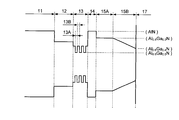
- FIG. 1 is a top view of a semiconductor light emitting device (hereinafter, simply referred to as a light emitting device) 10 according to a first embodiment.
- 2 is a cross-sectional view of the light emitting device 10, which is a cross-sectional view taken along the line WW of FIG.
- FIG. 3 is a band diagram of the light emitting element 10. The configuration of the light emitting element 10 will be described with reference to FIGS. 1 to 3.
- the light emitting device 10 is made of a nitride-based semiconductor having an emission wavelength band in the ultraviolet region (for example, within the range of 200 to 365 nm).
- the light emitting element 10 has an n-type semiconductor layer 12, an active layer 13, an electron block layer 14, and a p-type semiconductor layer 15 formed on a growth substrate 11.
- the n-type semiconductor layer 12 to the p-type semiconductor layer 15 function as a light emitting structure layer in the light emitting element 10.
- the light emitting element 10 has an n electrode 16 and ap electrode 17 which are connected to the n type semiconductor layer 12 and the p type semiconductor layer 15, respectively.
- the growth substrate 11 is made of, for example, an AlN substrate, a GaN substrate, a sapphire substrate, a SiC substrate, a Si substrate, or the like.
- the growth substrate 11 is a single crystal AlN substrate. That is, each of the n-type semiconductor layer 12 to the p-type semiconductor layer 15 is a semiconductor layer epitaxially grown on a single crystal AlN substrate as the growth substrate 11.
- the growth substrate 11 preferably has a relatively low dislocation density.
- the dislocation density of the growth substrate 11 is preferably 10 8 cm -2 or less, more preferably 10 7 cm -2 or less.
- the dislocation density can be measured using a known method such as measuring the number of dislocations from a transmission electron microscope image and measuring the number of etch pits measured after being immersed in a heated acid mixed solution. .
- the growth substrate 11 has the + C plane as a crystal growth plane. Therefore, in this embodiment, the n-type semiconductor layer 12 to the p-type semiconductor layer 15 are semiconductor layers grown on the C plane of the AlN substrate.
- the crystal growth surface of the growth substrate 11 is not limited to the + C surface, and a surface inclined (off) from the C surface may be used as the crystal growth surface.
- the inclination angle (off angle) is preferably within the range of 0.1 to 0.5 °, and within the range of 0.3 to 0.4 °. More preferably, The crystal growth surface of the growth substrate 11 may be the M surface or the A surface.
- the thickness of the growth substrate 11 can be determined in consideration of reducing the absorption coefficient of light and easiness of handling (yield).
- the thickness of the growth substrate 11 is preferably within the range of 50 to 1000 ⁇ m, for example.
- a buffer layer (not shown) may be provided between the growth substrate 11 and the n-type semiconductor layer 12.
- the buffer layer has, for example, a single-layer AlN layer, a superlattice structure of an AlN layer and an AlGaN layer, and a superlattice structure of AlGaN layers of different compositions, It is preferable to have a structure in which the composition is graded so that the Al composition decreases toward the n-type semiconductor layer 12, or a structure in which these are combined.
- the buffer layer is preferably made of, for example, an AlGaN layer having an Al composition higher than that of the n-type semiconductor layer 12.
- the buffer layer may have a composition that contributes to improving the yield of the crystal growth process of the n-type semiconductor layer 12 to the p-type semiconductor layer 15.
- the n-type semiconductor layer 12 is formed on the growth substrate 11.
- the n-type semiconductor layer 12 has a function of injecting electrons into the active layer 13.
- the n-type semiconductor layer 12 has a composition of Al s Ga 1 -s N (0 ⁇ s ⁇ 1, preferably x2 ⁇ s ⁇ 0.9, x2 is an Al composition of a barrier layer 13B of the active layer 13 described later). .
- the n-type semiconductor layer 12 has a composition of Al 0.7 Ga 0.3 N.
- the n-type semiconductor layer 12 preferably has a layer thickness of 100 nm or more, for example. Further, the n-type semiconductor layer 12 preferably has a low dislocation density.
- the n-type semiconductor layer 12 contains, for example, Si as an n-type dopant and has an n-type conductivity type.
- the dopant concentration of the n-type semiconductor layer 12 is not particularly limited and may be appropriately determined according to the purpose.
- the dopant concentration of the n-type semiconductor layer 12 is preferably in the range of 1 ⁇ 10 15 to 5 ⁇ 10 19 cm ⁇ 3 .
- the n-type semiconductor layer 12 may be composed of a plurality of semiconductor layers showing n-type conductivity.
- each of the semiconductor layers preferably has a dopant concentration in the range of 1 ⁇ 10 15 to 5 ⁇ 10 19 cm ⁇ 3 .
- the active layer 13 is formed on the n-type semiconductor layer 12 and has a band gap equal to or smaller than that of the n-type semiconductor layer 12.
- the active layer 13 functions as a light emitting layer.
- the active layer 13 has a crystal composition of AlGaN semiconductor.
- the active layer 13 has a composition of Al x Ga 1-x N (0 ⁇ x ⁇ 1).
- the active layer 13 emits light in the ultraviolet region.
- the active layer 13 is preferably formed directly on the n-type semiconductor layer 12, that is, in contact with the n-type semiconductor layer 12.
- the active layer 13 may contain In.
- the active layer 13 may have a composition of AlInGaN.
- the active layer 13 may have a band gap larger than that of GaN and smaller than that of AlN, for example. That is, the active layer 13 may have a crystal composition of an AlGaN semiconductor or an AlInGaN semiconductor.
- the active layer 13 has a multiple quantum well (MQW) structure.
- the active layer 13 includes a plurality of well layers 13A each having a composition of Al x1 Ga 1 -x1 N, and a well layer 13A each having a composition of Al x2 Ga 1 -x2 N. And a plurality of barrier layers 13B having a large band gap.
- each of the well layers 13A has a composition of Al 0.5 Ga 0.5 N
- each of the barrier layers 13B has a composition of Al 0.65 Ga 0.35 N.
- each of the well layers 13A has a layer thickness in the range of 3 to 6 nm
- each of the barrier layers 13B has a layer thickness in the range of 3 to 10 nm.
- the Al composition x2 of the barrier layer 13B is smaller than the Al composition s of the n-type semiconductor layer 12. Therefore, the barrier layer 13B has a smaller bandgap than the n-type semiconductor layer 12. Therefore, in this embodiment, a band gap step is provided between the n-type semiconductor layer 12 and the barrier layer 13B.
- the configuration of the active layer 13 is not limited to this.
- the active layer 13 is not limited to having a multiple quantum well structure.
- the active layer 13 may have a single quantum well structure or a single layer.
- the electron block layer 14 is formed on the active layer 13 and has a bandgap larger than that of the active layer 13.
- the electron block layer 14 has a composition of Al t Ga 1 -t N (s ⁇ t ⁇ 1).
- the electron block layer 14 functions as a layer for suppressing overflow of electrons injected into the active layer 13 to the p-type semiconductor layer 15.
- the electron block layer 14 contains, for example, Mg as a p-type dopant and has a p-type conductivity type.
- the electron block layer 14 may not include the p-type dopant, and may partially include the p-type dopant. Further, the electron block layer 14 may not be provided. That is, the p-type semiconductor layer 15 may be formed on the active layer 13.
- the p-type semiconductor layer 15 has a band gap equal to or smaller than that of the electron block layer 14.
- the p-type semiconductor layer 15 contains, for example, Mg as a p-type dopant and has a p-type conductivity type.
- the p-type semiconductor layer 15 functions as a clad layer together with the n-type semiconductor layer 12.
- the p-type semiconductor layer 15 is provided at the interface between the p-type clad layer 15A functioning as a clad layer and the p-electrode 17, and is in contact with the p-electrode 17 and electrically connected to the p-electrode 17.
- a contact layer 15B forming a contact.
- the p-type clad layer 15A has a composition of Al u Ga 1 -u N (x2 ⁇ u ⁇ 1, u ⁇ t). That is, the p-type clad layer 15A has a band gap equal to or smaller than the electron block layer 14.
- the p-type clad layer 15A has a composition of Al 0.8 Ga 0.2 N.
- the p-type cladding layer 15A has a layer thickness within the range of 1 to 100 nm.
- the band gap of the contact layer 15B monotonically decreases from the interface with the p-type cladding layer 15A toward the interface with the p-electrode 17 along the direction perpendicular to the p-type semiconductor layer 15 (the layer thickness direction of each layer). It has such a composition.
- the contact layer 15B has a composition within the range of Al y Ga 1-y N (0 ⁇ y ⁇ 1) so that the Al composition y decreases continuously toward the p-electrode 17. Is configured.
- the Al composition y of the contact layer 15B is configured to gradually decrease toward the p-electrode 17 within a range larger than the Al composition x1 of the well layer 13A in the active layer 13. That is, the Al composition y of the contact layer 15B is preferably changed within the range of x1 ⁇ y ⁇ 1.
- the contact layer 15B has a band gap larger than that of the well layer 13A as a whole.
- the contact layer 15B has a composition of Al 0.8 Ga 0.2 N (the same composition as the p-type cladding layer 15A) at the interface with the p-type cladding layer 15A. Further, the contact layer 15B has a composition of Al 0.6 Ga 0.4 N at the interface with the p electrode 17. That is, in the contact layer 15B, the Al composition y decreases from 0.8 to 0.6 toward the p electrode 17. Further, for example, the contact layer 15B has a layer thickness of 20 to 60 nm.
- the rate of change of Al composition y of dwell in the contact layer 15B is in the range of 0.0008nm -1 ⁇ 0.05nm -1.
- a preferable range of the rate of change of Al composition y in the contact layer 15B is 0.0008 nm -1 to 0.035 nm -1 , and a more preferable range is 0.003 nm -1.
- the range of up to 0.03 nm ⁇ 1 can be mentioned.
- the Al composition y of the contact layer 15B may be monotonically smaller toward the p-electrode 17.
- the Al composition y of the contact layer 15B is not limited to be continuously (linearly) reduced as shown in FIG. 3, and may be, for example, stepwise (stepwise) reduced. That is, for example, the contact layer 15B is an AlGaN layer having a composition such that the Al composition y decreases continuously or stepwise from the interface with the p-type cladding layer 15A toward the interface with the p-electrode 17.
- the band gaps of the n-type semiconductor layer 12, the active layer 13, the electron block layer 14, and the p-type semiconductor layer 15 are as shown in FIG. Have a relationship.
- the n-electrode 16 is formed on the n-type semiconductor layer 12, and the p-electrode 17 is formed on the p-type semiconductor layer 15 (contact layer 15B).
- the n electrode 16 is composed of a laminated body of a Ti layer, an Al layer and an Au layer.
- examples of the structure of the p electrode 17 include a laminated body of Ni layer and Au layer, a laminated body of Pt layer or Pd layer and Au layer.
- a metal oxide such as ITO is made extremely thin and then a material having reflectivity to ultraviolet light such as Al is laminated.
- a material such as a Rh layer or a Ru layer capable of forming a good ohmic contact with a p-type nitride semiconductor and having a high reflectance to ultraviolet light. It is preferable that
- the surface of the p-type semiconductor layer 15 penetrates the p-type semiconductor layer 15, the electron block layer 14, and the active layer 13 to reach the n-type semiconductor layer 12, and has a comb tooth shape in a top view.
- a concave portion (mesa structure portion) is formed.
- the n-electrode 16 is formed in a comb shape on the surface of the n-type semiconductor layer 12 exposed at the bottom of the recess.
- the p-electrode 17 is formed in a layered and comb-teeth shape on the surface of the p-type semiconductor layer 15 in which the recess is not formed, and the comb-teeth portion meshes with the comb-teeth portion of the n-electrode 16 in a top view.
- the light emitting element 10 has a support substrate (mounting substrate) 18 that supports the light emitting structure layer from the p-type semiconductor layer 15 side.
- the support substrate 18 has a base 18A and an n-side pad electrode 18B and a p-side pad electrode 18C formed on the base 18A and connected to the n-electrode 16 and the p-electrode 17, respectively.
- the light emitting element 10 has the connection electrode 19 that connects the n-side pad electrode 18B and the n-electrode 16. In other words, the light emitting element 10 is mounted by flip chip mounting.
- the above-described configurations of the n-type semiconductor layer 12 to the p-type semiconductor layer 15, and the configurations of the n-electrode 16 and the p-electrode 17 are merely examples.
- the n-electrode 16 may be in contact with the n-type semiconductor layer 12, and the p-electrode 17 may be in contact with the p-type semiconductor layer 15.
- the configuration (for example, electrode shape) of the light emitting element 10 illustrated in FIGS. 1 and 2 is merely an example.
- the support means and the mounting means of the light emitting element 10 are not limited to this.
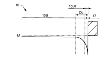
- FIG. 4 is a diagram schematically showing a band structure of a valence band in the vicinity of the contact layer 15B and the p electrode 17 of the light emitting element 10.
- the contact layer 15B will be described in detail with reference to FIG.
- the broken line in FIG. 4 indicates the Fermi level.
- the contact layer 15B is made of an AlGaN layer whose Al composition y gradually decreases toward the interface with the p-electrode 17.
- the inventor of the present application has found that forming the contact layer 15B as such a compositionally graded layer improves the electrode characteristics. It is considered that this is because the depletion layer DL formed in the contact layer 15B becomes extremely thin and a tunnel effect easily occurs at the interface with the p-electrode 17.
- AlGaN is a semiconductor material that has a larger bandgap as the Al composition is higher, and generally has a poor hole activation rate. Therefore, when AlGaN is formed as the contact layer 15B, a high energy barrier (Schottky barrier) is formed at the interface with the p electrode 17, and a thick depletion layer is easily formed. Therefore, ohmic contact with the p electrode 17 is difficult to be formed.
- a high energy barrier Schottky barrier
- the contact layer 15B has a composition in which the Al composition y decreases toward the p electrode 17. Therefore, the band gap of the contact layer 15B gradually decreases toward the p-electrode 17. As a result, the activation rate of holes in the contact layer 15B is significantly increased by the effect of the internal electric field, and the valence band and the Fermi level are close to each other. As a result, as shown in FIG. 4, it is considered that the energy band of the contact layer 15B largely bends near the interface with the p electrode 17.
- the depletion layer DL formed in the contact layer 15B becomes extremely thin, and holes easily cross the Schottky barrier due to the tunnel effect. Therefore, ohmic contact is formed between the contact layer 15B and the p electrode 17. That is, the contact layer 15B has a tunnel contact layer 15BT connected to the p electrode 17 by a tunnel junction near the interface with the p electrode 17.
- the tunnel contact layer 15BT is a region in the contact layer 15B where the tunnel effect occurs with a high probability, and its layer thickness changes depending on, for example, the material of the p-electrode P17, the composition of the contact layer 15B, and the applied current value. .
- the composition of the contact layer 15B as described above, it is possible to form the tunnel contact layer 15BT suitable for stably forming the ohmic contact.
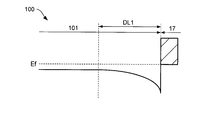
- FIG. 5 is a diagram showing a band structure of the light emitting device 100 according to the comparative example.
- the height of the energy barrier between the contact layer 101 and the p-electrode 17 is about the same as that of the contact layer 15B in this embodiment.
- the depletion layer DL1 formed in the contact layer 101 is much thicker than the depletion layer DL formed in the contact layer 15B. This is because the hole activation rate in the contact layer 101 is very low. Therefore, it can be expected that it is difficult to form a good ohmic contact between the contact layer 101 and the p electrode 17.
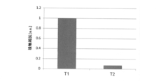
- FIG. 6A shows a p-AlGaN layer having a different composition in the layer like the contact layer 15B in the present example, and a p-AlGaN layer having a constant composition in the layer like the contact layer 101 in the comparative example.
- FIG. 6 is a diagram showing a measurement result of contact resistance between the p-electrode 17 and a metal layer made of the same material in FIG.
- FIG. 6 shows a p-AlGaN layer having a different composition in the layer and the metal having a contact resistance value of 1 between the p-AlGaN layer having a constant composition in the layer and the metal layer. It is a figure which shows the contact resistance value between layers.
- test structures T1 and T2 as shown in FIGS. 6B and 6C were prepared.
- FIG. 6B is a diagram showing the configuration of the test structure T1 including the p-AlGaN layer TL3 having the same composition as the contact layer 101 in the comparative example.
- FIG. 6C is a diagram showing the structure of the test structure T2 including the p-AlGaN layer TL4 having the same composition as the contact layer 15B in the example.
- the AlN buffer layer TL2 and the p-AlGaN layer TL3 are grown on the AlN substrate TL1, and the Ni layer and the Au layer are formed as the metal layer TE on the p-AlGaN layer TL3. It has a formed structure.
- the test structure T2 has a structure in which the AlN buffer layer TL2 and the p-AlGaN layer TL4 are grown on the AlN substrate TL1, and the metal layer TE is formed on the p-AlGaN layer TL4. .
- FIG. 6A shows the measurement results of the contact resistance between the p-AlGaN layer TL3 and the metal layer TE in the test structure T1 and the contact resistance between the p-AlGaN layer TL4 and the metal layer TE in the test structure T2.
- FIG. 6A shows the measurement results of the contact resistance between the p-AlGaN layer TL3 and the metal layer TE in the test structure T1 and the contact resistance between the p-AlGaN layer TL4 and the metal layer TE in the test structure T2.
- the contact resistance with the metal layer TE is significantly reduced as compared with the p-AlGaN layer TL3 having a constant composition.
- a good ohmic contact can be formed between the p-AlGaN layer TL4 and the metal layer TE having different compositions in the layer. That is, it can be seen that the contact layer 15B and the p electrode 17 can form a good ohmic contact. Therefore, by forming the contact layer 15B, it is possible to provide, for example, the light emitting element 10 having the contact layer 15B having a low driving voltage and high translucency.
- the contact layer 15B is preferably formed in a strained state. That is, it is preferable that the n-type semiconductor layer 12 to the p-type semiconductor layer 15 which are the light emitting structure layers are epitaxially grown in a pseudo lattice-matched state. Therefore, as in this embodiment, the n-type semiconductor layer 12, the active layer 13, the electron block layer 14, and the p-type semiconductor layer 15 are semiconductor layers epitaxially grown on a single crystal AlN substrate as the growth substrate 11. Preferably there is. Similarly, the contact layer 15B preferably has a composition of AlInGaN.
- the contact layer 15B (particularly in the vicinity of the interface in contact with the p electrode 17) preferably has a relatively high dopant concentration.
- the contact layer 15B preferably has a dopant concentration higher than that of the p-type cladding layer 15A.
- the contact layer 15B preferably has a higher dopant concentration than the p-type cladding layer 15A.
- the contact layer 15B preferably has the highest dopant concentration in the vicinity of the interface with the p electrode 17, that is, in the tunnel contact layer 15BT. In this case, the entire contact layer 15B need not have a higher dopant concentration than the p-type semiconductor layer 15A.
- the contact layer 15B may have a dopant concentration equal to or lower than or equal to the p-type cladding layer 15A in a region other than the tunnel contact layer 15BT, for example, in a region closer to the p-type cladding layer 15A than the tunnel contact layer 15BT. . That is, for example, the contact layer 15B preferably has a higher dopant concentration than the p-type cladding layer 15A in the vicinity of the interface with the p-electrode 17.
- FIG. 7 is a diagram schematically showing a path of light in the light emitting element 10. Note that, in FIG. 7, for the sake of explanation, only the path of light (reference numeral EL) emitted from the active layer 13 toward the p-type semiconductor layer 15 in the light emitting element 10 is shown.
- reference numeral EL reference numeral EL
- the contact layer 15B has a composition of AlGaN.
- the contact layer 15B has an Al composition larger than that of the well layer 13A of the active layer 13. Therefore, the contact layer 15B has a larger bandgap than the well layer 13A.
- the contact layer 15B receives almost no light emitted from the active layer 13 (reference numeral EL), that is, light having a wavelength corresponding to the band gap of the well layer 13A (light in the deep ultraviolet region in this embodiment). It has no absorbency. Therefore, most of the light (code EL) is transmitted through the contact layer 15B.
- the n-type semiconductor layer 12, the electron block layer 14, and the p-type semiconductor layer 15 are entirely transparent to the light emitted from the active layer 13.
- the p-electrode 17 has reflectivity for the light emitted from the active layer 13. Therefore, the light (reference numeral EL) transmitted through the p-type semiconductor layer 15 is reflected by the p-electrode 17 toward the n-type semiconductor layer 12 (growth substrate 11). Further, in this embodiment, the growth substrate 11 has a composition of AlN. Therefore, most of the light emitted from the active layer 13 is extracted outside through the growth substrate 11 without being absorbed in the light emitting element 10.
- the surface of the growth substrate 11 opposite to the n-type semiconductor layer 12 functions as a light extraction surface of the light emitting element 10. Then, light is emitted from this light extraction surface with high efficiency.
- the light emitting element 10 has the contact layer 15B whose composition gradually changes at the interface with the p-electrode 17. Therefore, a good ohmic contact can be formed between the light emitting structure layer and the electrode. Therefore, it is possible to suppress an increase in driving voltage and to form the contact layer 15B with less light absorption.
- the p-electrode 17 has reflectivity, the emitted light from the active layer 13 can be extracted from the light extraction surface with high efficiency. Therefore, it is possible to provide the light emitting element 10 having high luminous efficiency and high light extraction efficiency.
- the p-electrode 17 form a good ohmic contact and have high reflectivity. Therefore, for example, the material of the p electrode 17 may be selected in consideration of the relationship between the bandgap energy corresponding to the emission wavelength of the light emitting element 10 and the work function, and the reflectivity for the emission wavelength.
- examples of the material of the p-electrode 17 include Rh or Ru.
- the material of the p-electrode 17 is not limited to a material having reflectivity for the emission wavelength, but may be an electrode material capable of ensuring translucency by making it extremely thin.
- the p-electrode 17 may be a laminated body in which a metal oxide such as ITO and a metal such as Ni and Au are laminated with Al having a high reflectance.
- the light emitting element 10 has the emission wavelength band in the ultraviolet region, and the p-type semiconductor layer 15 has the contact layer 15B whose composition gradually changes at the interface with the p electrode 17. Further, the p electrode 17 has reflectivity for the light in the ultraviolet region. Therefore, it is possible to provide the light emitting device 10 with high output.
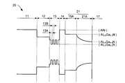
- FIG. 8 is a band diagram of the light emitting element 20 according to the second embodiment.
- the light emitting element 20 has the same configuration as the light emitting element 10 except for the configuration of the p-type semiconductor layer 21.
- the p-type semiconductor layer 21 has the same structure as the p-type semiconductor layer 15 except for the structure of the contact layer 21A.
- the reduction rate of Al composition y in the contact layer 21A gradually decreases from the interface with the p-type cladding layer 15A.
- the composition of the contact layer 21A on the p-type clad layer 15A side and the composition of the p-electrode 17 side are the same as those of the contact layer 15B. Therefore, the contact layer 21A exhibits a band gap as shown in FIG.
- the activation rate of holes in the contact layer 21A can also be increased by decreasing the Al composition y while gradually decreasing the reduction rate toward the interface with the p-electrode 17 as in the present embodiment. . Therefore, a good ohmic contact can be formed with the p electrode 17. Therefore, the light emitting element 20 with high output can be provided.
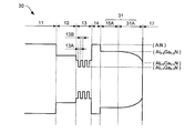
- FIG. 9 is a band diagram of the light emitting element 30 according to the third embodiment.
- the light emitting element 30 has the same configuration as the light emitting element 10 except for the configuration of the p-type semiconductor layer 31.
- the p-type semiconductor layer 31 has the same structure as the p-type semiconductor layer 15 except for the structure of the contact layer 31A.
- the decrease rate of Al composition y in the contact layer 31A gradually increases from the interface with the p-type cladding layer 15A.
- the composition of the contact layer 31A on the p-type clad layer 15A side and the composition of the p-electrode 17 side are the same as those of the contact layer 15B. Therefore, the contact layer 31A exhibits a band gap as shown in FIG.
- the activation rate of holes in the contact layer 31A can also be increased by decreasing the Al composition y while gradually increasing the decrease rate toward the interface with the p-electrode 17 as in the present embodiment. . Therefore, a good ohmic contact can be formed with the p electrode 17. Therefore, it is possible to provide the light emitting device 30 with high output.
- the contact layer 15A may be configured so that the Al composition y gradually decreases while the change rate changes. Even if the contact layer 15B is configured in this way, a tunnel contact layer similar to the tunnel contact layer 15BT is formed at the interface with the p electrode 17. Therefore, a good ohmic contact is formed between the p-type semiconductor layers 15, 21 and 31 and the p-electrode 17. Therefore, it is possible to provide the light emitting devices 10, 20 and 30 with high output.
- the contact layers 15B, 21A, and 31A have an Al composition y (that is, a band gap) larger than that of the well layer 13A of the active layer 13 as a whole.
- the contact layers 15B, 21A or 31A may partially have the Al composition y smaller than that of the well layer 13A.
- the contact layer 15B may have an Al composition y smaller than that of the well layer 13A in the vicinity of the interface with the p electrode 17. Even in this case, most of the light is transmitted through the contact layer 15B, and high light extraction efficiency can be obtained.
- each of the p-type semiconductor layers 15, 21 and 31 has an AlGaN layer having a constant Al composition u as the p-type cladding layer 15A has been described.
- the configuration of the p-type semiconductor layers 15, 21 and 31 is not limited to this.
- the p-type cladding layer 15A may be a composition gradient layer having a composition of AlGaN in which the Al composition u changes gradually.
- the entire p-type semiconductor layer 15 functions as a clad layer and a contact layer. That is, the p-type semiconductor layer 15 may not have the p-type clad layer 15A that functions only as a clad layer.
- the Al composition y of the contact layer 15B, 21A, or 31A has a larger rate of change than the Al composition u of the p-type cladding layer 15A in consideration of forming an ohmic contact. It is preferably changed.
- the p-type semiconductor layer 15, 21 or 31 is formed on the p-electrode 17, and the contact layer 15B, 21 or 21 is formed of an AlGaN layer whose Al composition y gradually decreases toward the interface with the p-electrode 17. It suffices to have 31A. Further, like the contact layer 15B, the contact layers 15B, 21A, and 31A may have the tunnel contact layer 15BT that is in contact with the p electrode 17 and is connected to the p electrode 17 by the tunnel junction.
- the p-type cladding layer 15A is provided in consideration of stably improving the light emission efficiency.
- the p-type semiconductor layer 15, 21 or 31 is formed closer to the active layer 13 than the contact layer 15B, 21A or 31A, and has a p-type cladding layer 15A having a higher dopant concentration than the contact layer 15B, 21A or 31A. It is preferable to have.
- the contact layers 15B, 21A, or 31A may have a higher dopant concentration than the p-type cladding layer 15A at the interface with the p-electrode 17.
- the dopant concentration of the contact layers 15B, 21A, or 31A changes, for example, in each layer (for example, toward the p-type clad layer 15A), and in the region other than the vicinity of the interface with the p-electrode 17, the p-type clad layer is formed. It may be smaller or smaller than the layer 15A.
- the p-type cladding layer 15A preferably has a higher dopant concentration than the contact layers 15B, 21A, or 31A.
- the electron block layer 14 that is, the semiconductor layer functioning as the electron block layer may not be provided, and the p-type semiconductor layer 15, 21 or 31 may be formed on the active layer 13.
- the p-type semiconductor layer 15, 21 or 31 may not contain Ga near the interface with the active layer 13. That is, the p-type semiconductor layer 15, 21 or 31 may partially have a composition of AlN.
- the contact layers 15B, 21A and 31A have the composition of AlGaN.
- the composition of the contact layers 15B, 21A and 31A is not limited to this.
- the contact layers 15B, 21A and 31A may have a composition such that the band gap gradually decreases toward the interface with the p-electrode 17.
- the contact layers 15B, 21A or 31A may have a composition of AlInGaN. That is, the contact layers 15B, 21A or 31A may contain In.
- the band gap in the contact layer 15B, 21A or 31A may be adjusted by adjusting the composition of Al and In.
- the contact layers 15B, 21A or 31A may be made of AlInGaN in which the Al composition gradually decreases toward the interface with the p-electrode 17 and the In composition gradually increases. Further, for example, the contact layers 15B, 21A or 31A may be made of AlInGaN whose Al composition gradually decreases toward the interface with the p-electrode 17.
- the p-type semiconductor layer 15, 21 or 31 may have a composition of AlN, AlGaN or AlInGaN.
- the contact layers 15A, 21A or 31A may have a composition of AlGaN or AlInGaN.
- the p-electrode 17 may be formed on the p-type semiconductor layer 15, 21 or 31.
- the p-type semiconductor layers 15, 21 and 31 may have the contact layers 15B, 21A and 31A in contact with the p-electrode 17.
- good ohmic contact is formed between the p-type semiconductor layers 15, 21 and 31 and the p-electrode 17, and the p-electrode 17 has reflectivity with respect to the light emitted from the active layer 13. High luminous efficiency can be obtained.
- the light emitting element 10 is formed on the n-type semiconductor layer 12 having the composition of AlGaN, the active layer 13 formed on the n-type semiconductor layer 12, and the active layer 13 made of an AlGaN-based semiconductor, and the active layer 13. And has a p-type semiconductor layer 15 having a composition of AlN, AlGaN, or AlInGaN, and a p-electrode 17 formed on the p-type semiconductor layer 15.
- the p-type semiconductor layer 15 has a contact layer 15B formed on the p-electrode 17 and made of an AlGaN layer or an AlInGaN layer having a band gap that decreases toward the interface with the p-electrode 17.
- the contact layer 15B has a tunnel contact layer 15BT which is in contact with the p electrode 17 and is connected to the p electrode 17 by a tunnel junction.
- the light emitting elements 20 and 30 have contact layers 21A and 31A similar to the contact layer 15. Therefore, it is possible to provide the light emitting devices 10, 20 and 30 in the ultraviolet region with high output.
Abstract
This semiconductor light-emitting element has: an n-type semiconductor layer that has an AlGaN or AlInGaN composition; an active layer that comprises an AlGaN-based semiconductor or an AlInGaN-based semiconductor and that is formed on an n-type semiconductor layer; a p-type semiconductor layer that has an AlN, AlGaN, or AlInGaN composition and that is formed on the active layer; and a p-electrode that is formed on the p-type semiconductor layer, wherein the p-type semiconductor layer has a contact layer that is formed on the p-electrode and that comprises an AlGaN layer or an AlInGaN layer with a band gap becoming smaller toward an interface with the p-electrode, and the contact layer has a tunnel contact layer that is in contact with the p-electrode and is connected to the p-electrode through a tunnel junction.
Description
本発明は、半導体発光素子、特に、紫外領域の光を放出する半導体発光素子に関する。
The present invention relates to a semiconductor light emitting device, particularly to a semiconductor light emitting device that emits light in the ultraviolet region.
近年、空気や水の殺菌作用を有する新しい光源として、紫外領域(例えばピーク波長が200nm~365nm)、特に深紫外領域(例えばピーク波長が200~300nm)に発光波長帯域を有する半導体発光素子が注目されている。例えば、特許文献1には、AlGaNの組成のp型コンタクト層を有し、深紫外領域に発光波長を有する発光素子が開示されている。
In recent years, as a new light source having a bactericidal action of air and water, a semiconductor light emitting element having an emission wavelength band in the ultraviolet region (for example, peak wavelength of 200 nm to 365 nm), particularly deep ultraviolet region (for example, peak wavelength of 200 to 300 nm) has attracted attention. Has been done. For example, Patent Document 1 discloses a light emitting element having a p-type contact layer having a composition of AlGaN and having an emission wavelength in the deep ultraviolet region.
紫外領域に発光波長を有する半導体発光素子は、高出力化の点で課題を有している。特に、窒化物系半導体からなる紫外発光素子においては、活性層から放出された光が外部に取り出されにくいこと、すなわち光取出し効率が低いことが課題の1つとして挙げられる。
-Semiconductor light-emitting devices having an emission wavelength in the ultraviolet region have a problem in terms of high output. Particularly, in the ultraviolet light emitting device made of a nitride semiconductor, one of the problems is that the light emitted from the active layer is difficult to be extracted to the outside, that is, the light extraction efficiency is low.
本発明は上記した点に鑑みてなされたものであり、高出力な紫外領域の半導体発光素子を提供することを目的としている。
The present invention has been made in view of the above points, and an object thereof is to provide a semiconductor light emitting device in the ultraviolet region with high output.
本発明による半導体発光素子は、AlGaN又はAlInGaNの組成を有するn型半導体層と、n型半導体層上に形成され、AlGaN系半導体又はAlInGaN系半導体からなる活性層と、活性層上に形成され、AlN、AlGaN又はAlInGaNの組成を有するp型半導体層と、p型半導体層上に形成されたp電極と、を有し、p型半導体層は、p電極上に形成され、p電極との界面に向かってバンドギャップが小さくなるAlGaN層又はAlInGaN層からなるコンタクト層を有し、コンタクト層は、p電極に接触し、トンネル接合によってp電極に接続されたトンネルコンタクト層を有することを特徴としている。
A semiconductor light emitting device according to the present invention is formed on an n-type semiconductor layer having a composition of AlGaN or AlInGaN, an n-type semiconductor layer, an active layer made of an AlGaN-based semiconductor or an AlInGaN-based semiconductor, and an active layer, It has a p-type semiconductor layer having a composition of AlN, AlGaN, or AlInGaN, and a p-electrode formed on the p-type semiconductor layer, and the p-type semiconductor layer is formed on the p-electrode and has an interface with the p-electrode. Is characterized by having a contact layer made of an AlGaN layer or an AlInGaN layer whose band gap becomes smaller toward the side, and the contact layer has a tunnel contact layer that is in contact with the p electrode and is connected to the p electrode by a tunnel junction. .
以下、本発明の実施例について詳細に説明する。
The embodiments of the present invention will be described in detail below.
図1は、実施例1に係る半導体発光素子(以下、単に発光素子と称する)10の上面図である。また、図2は、発光素子10の断面図であり、図1のW-W線に沿った断面図である。また、図3は、発光素子10のバンド図である。図1乃至図3を用いて、発光素子10の構成について説明する。
FIG. 1 is a top view of a semiconductor light emitting device (hereinafter, simply referred to as a light emitting device) 10 according to a first embodiment. 2 is a cross-sectional view of the light emitting device 10, which is a cross-sectional view taken along the line WW of FIG. Further, FIG. 3 is a band diagram of the light emitting element 10. The configuration of the light emitting element 10 will be described with reference to FIGS. 1 to 3.
まず、発光素子10の構造について説明する。本実施例においては、発光素子10は、紫外領域(例えば200~365nmの範囲内)に発光波長帯域を有する窒化物系半導体
からなる。 First, the structure of thelight emitting element 10 will be described. In the present embodiment, the light emitting device 10 is made of a nitride-based semiconductor having an emission wavelength band in the ultraviolet region (for example, within the range of 200 to 365 nm).
からなる。 First, the structure of the
発光素子10は、成長用基板11上に形成されたn型半導体層12、活性層13、電子ブロック層14及びp型半導体層15を有する。n型半導体層12乃至p型半導体層15は、発光素子10における発光構造層として機能する。また、発光素子10は、n型半導体層12及びp型半導体層15にそれぞれ接続されたn電極16及びp電極17を有する。
The light emitting element 10 has an n-type semiconductor layer 12, an active layer 13, an electron block layer 14, and a p-type semiconductor layer 15 formed on a growth substrate 11. The n-type semiconductor layer 12 to the p-type semiconductor layer 15 function as a light emitting structure layer in the light emitting element 10. Further, the light emitting element 10 has an n electrode 16 and ap electrode 17 which are connected to the n type semiconductor layer 12 and the p type semiconductor layer 15, respectively.
まず、本実施例においては、成長用基板11は、例えば、AlN基板、GaN基板、サファイア基板、SiC基板、Si基板などからなる。本実施例においては、成長用基板11は単結晶のAlN基板である。すなわち、n型半導体層12乃至p型半導体層15の各々は、成長用基板11としての単結晶のAlN基板上にエピタキシャル成長された半導体層である。
First, in this embodiment, the growth substrate 11 is made of, for example, an AlN substrate, a GaN substrate, a sapphire substrate, a SiC substrate, a Si substrate, or the like. In this embodiment, the growth substrate 11 is a single crystal AlN substrate. That is, each of the n-type semiconductor layer 12 to the p-type semiconductor layer 15 is a semiconductor layer epitaxially grown on a single crystal AlN substrate as the growth substrate 11.
なお、高い結晶品質のn型半導体層12乃至p型半導体層15を成長させることを考慮すると、成長用基板11は、比較的低い転位密度を有することが好ましい。例えば、成長用基板11の転位密度は、108cm-2以下であることが好ましく、107cm-2以下であることがさらに好ましい。なお、転位密度は、透過型電子顕微鏡像より転位数を測定すること、及び加熱酸混合溶液に浸漬した後に測定したエッチピット数を測定することなど、公知の方法を用いて測定することができる。
In consideration of growing the n-type semiconductor layer 12 to the p-type semiconductor layer 15 having high crystal quality, the growth substrate 11 preferably has a relatively low dislocation density. For example, the dislocation density of the growth substrate 11 is preferably 10 8 cm -2 or less, more preferably 10 7 cm -2 or less. The dislocation density can be measured using a known method such as measuring the number of dislocations from a transmission electron microscope image and measuring the number of etch pits measured after being immersed in a heated acid mixed solution. .
また、本実施例においては、成長用基板11は、+C面を結晶成長面として有する。従って、本実施例においては、n型半導体層12乃至p型半導体層15は、AlN基板のC面上に成長された半導体層である。しかし、成長用基板11の結晶成長面は+C面である場合に限定されず、例えばC面から傾斜(オフ)した面を結晶成長面として用いてもよい。+C面から傾斜した面を結晶成長面として用いる場合、その傾斜角(オフ角)は、0.1~0.5°の範囲内であることが好ましく、0.3~0.4°の範囲内であることがさらに好ましい。また、成長用基板11の結晶成長面は、M面又はA面であってもよい。
Further, in this embodiment, the growth substrate 11 has the + C plane as a crystal growth plane. Therefore, in this embodiment, the n-type semiconductor layer 12 to the p-type semiconductor layer 15 are semiconductor layers grown on the C plane of the AlN substrate. However, the crystal growth surface of the growth substrate 11 is not limited to the + C surface, and a surface inclined (off) from the C surface may be used as the crystal growth surface. When a plane inclined from the + C plane is used as a crystal growth plane, the inclination angle (off angle) is preferably within the range of 0.1 to 0.5 °, and within the range of 0.3 to 0.4 °. More preferably, The crystal growth surface of the growth substrate 11 may be the M surface or the A surface.
また、成長用基板11の厚さは、光の吸収係数を小さくすること、及び取り扱いの容易さ(歩留まり)などを考慮して定めることができる。成長用基板11の厚さは、例えば、50~1000μmの範囲内であることが好ましい。
Further, the thickness of the growth substrate 11 can be determined in consideration of reducing the absorption coefficient of light and easiness of handling (yield). The thickness of the growth substrate 11 is preferably within the range of 50 to 1000 μm, for example.
なお、成長用基板11とn型半導体層12との間には、バッファ層(図示せず)が設けられていてもよい。バッファ層を設ける場合、バッファ層は、例えば、単層のAlN層からなること、AlN層及びAlGaN層からなる超格子構造を有すること、互いに異なる組成のAlGaN層からなる超格子構造を有すること、n型半導体層12に向かってAl組成が減少するように組成が傾斜する構造を有すること、又はこれらの組み合わせた構造を有することが好ましい。また、バッファ層は、例えば、n型半導体層12よりも高いAl組成のAlGaN層からなることが好ましい。しかし、バッファ層は、n型半導体層12乃至p型半導体層15の結晶成長プロセスの歩留まり向上に寄与するような組成を有していればよい。
A buffer layer (not shown) may be provided between the growth substrate 11 and the n-type semiconductor layer 12. When the buffer layer is provided, the buffer layer has, for example, a single-layer AlN layer, a superlattice structure of an AlN layer and an AlGaN layer, and a superlattice structure of AlGaN layers of different compositions, It is preferable to have a structure in which the composition is graded so that the Al composition decreases toward the n-type semiconductor layer 12, or a structure in which these are combined. The buffer layer is preferably made of, for example, an AlGaN layer having an Al composition higher than that of the n-type semiconductor layer 12. However, the buffer layer may have a composition that contributes to improving the yield of the crystal growth process of the n-type semiconductor layer 12 to the p-type semiconductor layer 15.
また、バッファ層を設ける場合、バッファ層は、例えば生産性を考慮すると、1~10000nmの範囲内の層厚を有することが好ましく、10~5000nmの範囲内の層厚を有することがさらに好ましい。
When the buffer layer is provided, the buffer layer preferably has a layer thickness in the range of 1 to 10000 nm, more preferably 10 to 5000 nm in consideration of productivity, for example.
図2及び図3を参照すると、n型半導体層12は、成長用基板11上に形成されている。n型半導体層12は、活性層13に電子を注入する機能を有する。
Referring to FIGS. 2 and 3, the n-type semiconductor layer 12 is formed on the growth substrate 11. The n-type semiconductor layer 12 has a function of injecting electrons into the active layer 13.
n型半導体層12は、AlsGa1-sN(0<s<1、好ましくはx2≦s≦0.9、x2は後述する活性層13の障壁層13BのAl組成)の組成を有する。本実施例においては、n型半導体層12は、Al0.7Ga0.3Nの組成を有する。n型半導体層12は、例えば、100nm以上の層厚を有することが好ましい。また、n型半導体層12は、低い転位密度を有することが好ましい。
The n-type semiconductor layer 12 has a composition of Al s Ga 1 -s N (0 <s <1, preferably x2 ≦ s ≦ 0.9, x2 is an Al composition of a barrier layer 13B of the active layer 13 described later). . In this example, the n-type semiconductor layer 12 has a composition of Al 0.7 Ga 0.3 N. The n-type semiconductor layer 12 preferably has a layer thickness of 100 nm or more, for example. Further, the n-type semiconductor layer 12 preferably has a low dislocation density.
なお、n型半導体層12は、Inを含んでいてもよい。例えば、n型半導体層12は、AlInGaNの組成を有していてもよい。この場合であっても、n型半導体層12は、例えば、活性層13の障壁層13B以上であり、かつAl0.9Ga0.1N以下のバンドギャップを有していることが好ましい。すなわち、n型半導体層12は、AlGaN又はAlInGaNの組成を有していればよい。
The n-type semiconductor layer 12 may contain In. For example, the n-type semiconductor layer 12 may have a composition of AlInGaN. Even in this case, it is preferable that the n-type semiconductor layer 12 has a band gap that is, for example, not less than the barrier layer 13B of the active layer 13 and not more than Al 0.9 Ga 0.1 N. That is, the n-type semiconductor layer 12 may have a composition of AlGaN or AlInGaN.
n型半導体層12は、n型ドーパントとして例えばSiを含み、n型の導電型を有する。n型半導体層12のドーパント濃度は、特に制限されるものではなく、目的に応じて適宜決定すればよい。例えば、高い導電性を得ることを考慮すると、n型半導体層12のドーパント濃度は、1×10¹⁵~5×1019cm-3の範囲内であることが好ましい。
The n-type semiconductor layer 12 contains, for example, Si as an n-type dopant and has an n-type conductivity type. The dopant concentration of the n-type semiconductor layer 12 is not particularly limited and may be appropriately determined according to the purpose. For example, in consideration of obtaining high conductivity, the dopant concentration of the n-type semiconductor layer 12 is preferably in the range of 1 × 10 15 to 5 × 10 19 cm −3 .
なお、n型半導体層12は、複数のn型の導電型を示す半導体層から構成されていてもよい。この場合、そのそれぞれの半導体層は、1×10¹⁵~5×1019cm-3の範囲内のドーパント濃度を有することが好ましい。
The n-type semiconductor layer 12 may be composed of a plurality of semiconductor layers showing n-type conductivity. In this case, each of the semiconductor layers preferably has a dopant concentration in the range of 1 × 10 15 to 5 × 10 19 cm −3 .
活性層13は、n型半導体層12上に形成され、n型半導体層12以下のバンドギャップを有する。活性層13は、発光層として機能する。本実施例においては、活性層13は、AlGaN系半導体からなる結晶組成を有する。具体的には、活性層13は、AlxGa1-xN(0<x<1)の組成を有する。活性層13は、紫外領域の光を放出する。なお、活性層13は、n型半導体層12上に直接形成されていること、すなわちn型半導体層12に接していることが好ましい。
The active layer 13 is formed on the n-type semiconductor layer 12 and has a band gap equal to or smaller than that of the n-type semiconductor layer 12. The active layer 13 functions as a light emitting layer. In this embodiment, the active layer 13 has a crystal composition of AlGaN semiconductor. Specifically, the active layer 13 has a composition of Al x Ga 1-x N (0 <x <1). The active layer 13 emits light in the ultraviolet region. The active layer 13 is preferably formed directly on the n-type semiconductor layer 12, that is, in contact with the n-type semiconductor layer 12.
なお、活性層13は、Inを含んでいてもよい。例えば、活性層13は、AlInGaNの組成を有していてもよい。この場合であっても、活性層13は、例えば、GaNよりも大きく、かつAlNよりも小さなバンドギャップを有していればよい。すなわち、活性層13は、AlGaN系半導体又はAlInGaN系半導体からなる結晶組成を有していればよい。
The active layer 13 may contain In. For example, the active layer 13 may have a composition of AlInGaN. Even in this case, the active layer 13 may have a band gap larger than that of GaN and smaller than that of AlN, for example. That is, the active layer 13 may have a crystal composition of an AlGaN semiconductor or an AlInGaN semiconductor.
また、本実施例においては、図3に示すように、活性層13は、多重量子井戸(MQW)構造を有する。本実施例においては、活性層13は、各々がAlx1Ga1-x1Nの組成を有する複数の井戸層13Aと、各々がAlx2Ga1-x2Nの組成を有しかつ井戸層13Aよりも大きなバンドギャップを有する複数の障壁層13Bと、を含む。
Further, in the present embodiment, as shown in FIG. 3, the active layer 13 has a multiple quantum well (MQW) structure. In this embodiment, the active layer 13 includes a plurality of well layers 13A each having a composition of Al x1 Ga 1 -x1 N, and a well layer 13A each having a composition of Al x2 Ga 1 -x2 N. And a plurality of barrier layers 13B having a large band gap.
本実施例においては、井戸層13Aの各々はAl0.5Ga0.5Nの組成を有し、障壁層13Bの各々はAl0.65Ga0.35Nの組成を有する。また、例えば、井戸層13Aの各々は3~6nmの範囲内の層厚を有し、障壁層13Bの各々は3~10nmの範囲内の層厚を有する。
In this embodiment, each of the well layers 13A has a composition of Al 0.5 Ga 0.5 N, and each of the barrier layers 13B has a composition of Al 0.65 Ga 0.35 N. Further, for example, each of the well layers 13A has a layer thickness in the range of 3 to 6 nm, and each of the barrier layers 13B has a layer thickness in the range of 3 to 10 nm.
また、本実施例においては、障壁層13BのAl組成x2は、n型半導体層12のAl組成sよりも小さい。従って、障壁層13Bは、n型半導体層12よりも小さなバンドギャップを有する。従って、本実施例においては、n型半導体層12と障壁層13Bとの間にバンドギャップの段差が設けられている。
Further, in this embodiment, the Al composition x2 of the barrier layer 13B is smaller than the Al composition s of the n-type semiconductor layer 12. Therefore, the barrier layer 13B has a smaller bandgap than the n-type semiconductor layer 12. Therefore, in this embodiment, a band gap step is provided between the n-type semiconductor layer 12 and the barrier layer 13B.
なお、活性層13の構成はこれに限定されない。例えば、活性層13は、多重量子井戸構造を有する場合に限定されない。例えば、活性層13は、単一量子井戸構造を有していてもよく、また、単層からなっていてもよい。
The configuration of the active layer 13 is not limited to this. For example, the active layer 13 is not limited to having a multiple quantum well structure. For example, the active layer 13 may have a single quantum well structure or a single layer.
電子ブロック層14は、活性層13上に形成され、活性層13よりも大きなバンドギャップを有する。電子ブロック層14は、AltGa1-tN(s<t≦1)の組成を有する。電子ブロック層14は、活性層13内に注入された電子のp型半導体層15へのオーバーフローを抑制する層として機能する。
The electron block layer 14 is formed on the active layer 13 and has a bandgap larger than that of the active layer 13. The electron block layer 14 has a composition of Al t Ga 1 -t N (s <t ≦ 1). The electron block layer 14 functions as a layer for suppressing overflow of electrons injected into the active layer 13 to the p-type semiconductor layer 15.
本実施例においては、電子ブロック層14は、n型半導体層12よりも大きなバンドギャップを有する。また、本実施例においては、電子ブロック層14は、成長用基板11と同一の組成、すなわちAlNの組成を有する(t=1の場合に対応する)。また、例えば、電子ブロック層14は、1~50nmの範囲内の層厚を有する。
In this embodiment, the electron block layer 14 has a larger bandgap than the n-type semiconductor layer 12. Further, in this embodiment, the electron block layer 14 has the same composition as the growth substrate 11, that is, the composition of AlN (corresponding to the case of t = 1). Further, for example, the electron block layer 14 has a layer thickness within the range of 1 to 50 nm.
なお、本実施例においては、電子ブロック層14は、p型ドーパントとして例えばMgを含み、p型の導電型を有する。しかし、電子ブロック層14は、p型ドーパントを含んでいなくてもよく、また、その一部にp型ドーパントを含んでいてもよい。また、電子ブロック層14は、設けられていなくてもよい。すなわち、活性層13上にp型半導体層15が形成されていてもよい。
In the present embodiment, the electron block layer 14 contains, for example, Mg as a p-type dopant and has a p-type conductivity type. However, the electron block layer 14 may not include the p-type dopant, and may partially include the p-type dopant. Further, the electron block layer 14 may not be provided. That is, the p-type semiconductor layer 15 may be formed on the active layer 13.
p型半導体層15は、電子ブロック層14以下のバンドギャップを有する。p型半導体層15は、p型ドーパントとして例えばMgを含み、p型の導電型を有する。p型半導体層15は、n型半導体層12と共に、クラッド層として機能する。また、本実施例においては、p型半導体層15は、クラッド層として機能するp型クラッド層15Aと、p電極17との界面に設けられてp電極17に接し、p電極17との電気的接触を形成するコンタクト層15Bとを有する。
The p-type semiconductor layer 15 has a band gap equal to or smaller than that of the electron block layer 14. The p-type semiconductor layer 15 contains, for example, Mg as a p-type dopant and has a p-type conductivity type. The p-type semiconductor layer 15 functions as a clad layer together with the n-type semiconductor layer 12. In addition, in the present embodiment, the p-type semiconductor layer 15 is provided at the interface between the p-type clad layer 15A functioning as a clad layer and the p-electrode 17, and is in contact with the p-electrode 17 and electrically connected to the p-electrode 17. A contact layer 15B forming a contact.
p型クラッド層15Aは、AluGa1-uN(x2<u<1、u≦t)の組成を有する。すなわち、p型クラッド層15Aは、電子ブロック層14以下のバンドギャップを有する。例えば、p型クラッド層15Aは、Al0.8Ga0.2Nの組成を有する。また、例えば、p型クラッド層15Aは、1~100nmの範囲内の層厚を有する。
The p-type clad layer 15A has a composition of Al u Ga 1 -u N (x2 <u <1, u ≦ t). That is, the p-type clad layer 15A has a band gap equal to or smaller than the electron block layer 14. For example, the p-type clad layer 15A has a composition of Al 0.8 Ga 0.2 N. Further, for example, the p-type cladding layer 15A has a layer thickness within the range of 1 to 100 nm.
コンタクト層15Bは、p型クラッド層15Aとの界面からp電極17との界面に向かって、p型半導体層15に垂直な方向(各層の層厚方向)に沿ってバンドギャップが単調に小さくなるような組成を有する。本実施例においては、コンタクト層15Bは、AlyGa1-yN(0≦y≦1)の範囲内の組成を有し、p電極17に向かって連続的にAl組成yが小さくなるように構成されている。
The band gap of the contact layer 15B monotonically decreases from the interface with the p-type cladding layer 15A toward the interface with the p-electrode 17 along the direction perpendicular to the p-type semiconductor layer 15 (the layer thickness direction of each layer). It has such a composition. In this embodiment, the contact layer 15B has a composition within the range of Al y Ga 1-y N (0 ≦ y ≦ 1) so that the Al composition y decreases continuously toward the p-electrode 17. Is configured.
また、コンタクト層15BのAl組成yは、活性層13における井戸層13AのAl組成x1よりも大きい範囲内で、p電極17に向かって徐々に小さくなるように構成されていることが好ましい。すなわち、コンタクト層15BのAl組成yは、x1≦y≦1の範囲内で変化していることが好ましい。
Further, it is preferable that the Al composition y of the contact layer 15B is configured to gradually decrease toward the p-electrode 17 within a range larger than the Al composition x1 of the well layer 13A in the active layer 13. That is, the Al composition y of the contact layer 15B is preferably changed within the range of x1 ≦ y ≦ 1.
これによって、コンタクト層15Bは、全体として、井戸層13Aよりも大きなバンドギャップを有することとなる。コンタクト層15BのAl組成yをx1≦y≦1の範囲内で変化させることで、活性層13から放出された光の波長に対して透光性を持たせることができる。従って、発光素子10の光取り出し効率が向上する。
As a result, the contact layer 15B has a band gap larger than that of the well layer 13A as a whole. By changing the Al composition y of the contact layer 15B within the range of x1 ≦ y ≦ 1, it is possible to give a light transmitting property to the wavelength of the light emitted from the active layer 13. Therefore, the light extraction efficiency of the light emitting element 10 is improved.
本実施例においては、コンタクト層15Bは、p型クラッド層15Aとの界面においては、Al0.8Ga0.2Nの組成(p型クラッド層15Aと同一の組成)を有する。また、コンタクト層15Bは、p電極17との界面においては、Al0.6Ga0.4Nの組成を有する。すなわち、コンタクト層15B内において、Al組成yは、p電極17に向かって、0.8から0.6まで減少している。また、例えば、コンタクト層15Bは、20~60nmの層厚を有する。
In this embodiment, the contact layer 15B has a composition of Al 0.8 Ga 0.2 N (the same composition as the p-type cladding layer 15A) at the interface with the p-type cladding layer 15A. Further, the contact layer 15B has a composition of Al 0.6 Ga 0.4 N at the interface with the p electrode 17. That is, in the contact layer 15B, the Al composition y decreases from 0.8 to 0.6 toward the p electrode 17. Further, for example, the contact layer 15B has a layer thickness of 20 to 60 nm.
また、例えば、コンタクト層15B内におるAl組成yの変化率(減少率)は、0.0008nm-1~0.05nm-1の範囲内である。また、コンタクト層15BにおけるAl組成yの変化率の好ましい範囲としては、0.0008nm-1~0.035nm-1の範囲を挙げることができ、また、より好ましい範囲としては、0.003nm-1~0.03nm-1の範囲を挙げることができる。
Further, for example, the rate of change of Al composition y of dwell in the contact layer 15B (reduction rate) is in the range of 0.0008nm -1 ~ 0.05nm -1. A preferable range of the rate of change of Al composition y in the contact layer 15B is 0.0008 nm -1 to 0.035 nm -1 , and a more preferable range is 0.003 nm -1. The range of up to 0.03 nm −1 can be mentioned.
なお、コンタクト層15BのAl組成yは、p電極17に向かって単調に小さくなっていればよい。例えば、コンタクト層15BのAl組成yは、図3に示すように連続的(線形的)に小さくなっている場合に限定されず、例えば段階的(階段状)に小さくなっていてもよい。すなわち、例えば、コンタクト層15Bは、p型クラッド層15Aとの界面からp電極17との界面に向かって連続的又は段階的にAl組成yが小さくなるような組成を有するAlGaN層である。
The Al composition y of the contact layer 15B may be monotonically smaller toward the p-electrode 17. For example, the Al composition y of the contact layer 15B is not limited to be continuously (linearly) reduced as shown in FIG. 3, and may be, for example, stepwise (stepwise) reduced. That is, for example, the contact layer 15B is an AlGaN layer having a composition such that the Al composition y decreases continuously or stepwise from the interface with the p-type cladding layer 15A toward the interface with the p-electrode 17.
本実施例においては、n型半導体層12、活性層13、電子ブロック層14、及びp型半導体層15(p型クラッド層15A及びコンタクト層15B)の各々のバンドギャップは、図3に示すような関係を有する。
In this embodiment, the band gaps of the n-type semiconductor layer 12, the active layer 13, the electron block layer 14, and the p-type semiconductor layer 15 (p-type cladding layer 15A and contact layer 15B) are as shown in FIG. Have a relationship.
また、図1及び図2を参照すると、n電極16は、n型半導体層12上に形成され、p電極17はp型半導体層15(コンタクト層15B)上に形成されている。例えば、n電極16は、Ti層、Al層及びAu層の積層体からなる。
Further, referring to FIGS. 1 and 2, the n-electrode 16 is formed on the n-type semiconductor layer 12, and the p-electrode 17 is formed on the p-type semiconductor layer 15 (contact layer 15B). For example, the n electrode 16 is composed of a laminated body of a Ti layer, an Al layer and an Au layer.
また、p電極17の構成例としては、例えば、Ni層及びAu層の積層体、Pt層又はPd層とAu層との積層体が挙げられる。また、p電極17の他の構成例としては、ITOなどの金属酸化物を極めて薄くした後、Alなどの紫外光に対して反射性を有する材料を積層したものが挙げられる。なお、p電極17としては、Rh層又はRu層など、p型の窒化物半導体との間で良好なオーミックコンタクトを形成することが可能であり、かつ紫外光に対して高い反射率を有する材料で構成されることが好ましい。
Further, examples of the structure of the p electrode 17 include a laminated body of Ni layer and Au layer, a laminated body of Pt layer or Pd layer and Au layer. Further, as another configuration example of the p-electrode 17, there may be mentioned one in which a metal oxide such as ITO is made extremely thin and then a material having reflectivity to ultraviolet light such as Al is laminated. As the p electrode 17, a material such as a Rh layer or a Ru layer capable of forming a good ohmic contact with a p-type nitride semiconductor and having a high reflectance to ultraviolet light. It is preferable that
本実施例においては、p型半導体層15の表面には、p型半導体層15、電子ブロック層14、活性層13を貫通してn型半導体層12に至り、上面視において櫛歯形状を有する凹部(メサ構造部)が形成されている。n電極16は、当該凹部の底部において露出したn型半導体層12の表面上において櫛歯状に形成されている。
In the present embodiment, the surface of the p-type semiconductor layer 15 penetrates the p-type semiconductor layer 15, the electron block layer 14, and the active layer 13 to reach the n-type semiconductor layer 12, and has a comb tooth shape in a top view. A concave portion (mesa structure portion) is formed. The n-electrode 16 is formed in a comb shape on the surface of the n-type semiconductor layer 12 exposed at the bottom of the recess.
また、p電極17は、当該凹部が形成されていないp型半導体層15の表面上に層状にかつ櫛歯状に形成され、上面視においてその櫛歯部分がn電極16の櫛歯部分に噛み合うように配置されている。
The p-electrode 17 is formed in a layered and comb-teeth shape on the surface of the p-type semiconductor layer 15 in which the recess is not formed, and the comb-teeth portion meshes with the comb-teeth portion of the n-electrode 16 in a top view. Are arranged as follows.
また、本実施例においては、発光素子10は、p型半導体層15側から発光構造層を支持する支持基板(実装用基板)18を有する。支持基板18は、基体18Aと、基体18A上に形成され、それぞれn電極16及びp電極17に接続されたn側パッド電極18B及びp側パッド電極18Cを有する。また、本実施例においては、発光素子10は、n側パッド電極18Bとn電極16とを接続する接続電極19を有する。換言すれば、発光素子10は、フリップチップ実装によって実装されている。
In addition, in the present embodiment, the light emitting element 10 has a support substrate (mounting substrate) 18 that supports the light emitting structure layer from the p-type semiconductor layer 15 side. The support substrate 18 has a base 18A and an n-side pad electrode 18B and a p-side pad electrode 18C formed on the base 18A and connected to the n-electrode 16 and the p-electrode 17, respectively. In addition, in the present embodiment, the light emitting element 10 has the connection electrode 19 that connects the n-side pad electrode 18B and the n-electrode 16. In other words, the light emitting element 10 is mounted by flip chip mounting.
なお、上記したn型半導体層12乃至p型半導体層15の構成、並びにn電極16及びp電極17の構成は、一例に過ぎない。例えば、n電極16はn型半導体層12に接していればよく、p電極17はp型半導体層15に接していればよい。すなわち、例えば図1及び図2に示す発光素子10の構成(例えば電極形状など)は一例に過ぎない。また、発光素子10の支持手段及び実装手段はこれに限定されない。
The above-described configurations of the n-type semiconductor layer 12 to the p-type semiconductor layer 15, and the configurations of the n-electrode 16 and the p-electrode 17 are merely examples. For example, the n-electrode 16 may be in contact with the n-type semiconductor layer 12, and the p-electrode 17 may be in contact with the p-type semiconductor layer 15. That is, for example, the configuration (for example, electrode shape) of the light emitting element 10 illustrated in FIGS. 1 and 2 is merely an example. Further, the support means and the mounting means of the light emitting element 10 are not limited to this.
図4は、発光素子10のコンタクト層15B及びp電極17の近傍における価電子帯のバンド構造を模式的に示す図である。図4を用いて、コンタクト層15Bについて詳細に説明する。図4の破線は、フェルミ準位を示す。
FIG. 4 is a diagram schematically showing a band structure of a valence band in the vicinity of the contact layer 15B and the p electrode 17 of the light emitting element 10. The contact layer 15B will be described in detail with reference to FIG. The broken line in FIG. 4 indicates the Fermi level.
本実施例においては、コンタクト層15Bは、p電極17との界面に向かってAl組成yが徐々に小さくなるAlGaN層からなる。本願の発明者は、コンタクト層15Bをこのような組成傾斜層として形成すると、電極特性が良化することを見出した。これは、コンタクト層15Bに形成される空乏層DLが非常に薄くなり、p電極17との界面において容易にトンネル効果が発生することによると考えられる。
In this embodiment, the contact layer 15B is made of an AlGaN layer whose Al composition y gradually decreases toward the interface with the p-electrode 17. The inventor of the present application has found that forming the contact layer 15B as such a compositionally graded layer improves the electrode characteristics. It is considered that this is because the depletion layer DL formed in the contact layer 15B becomes extremely thin and a tunnel effect easily occurs at the interface with the p-electrode 17.
より具体的には、AlGaNは、Al組成が高いほど大きなバンドギャップを有し、かつ一般に、正孔の活性化率が悪い半導体材料である。従って、AlGaNをコンタクト層15Bとして形成すると、p電極17との界面において高いエネルギー障壁(ショットキー障壁)が形成され、また厚い空乏層が形成されやすい。従って、p電極17とのオーミックコンタクトが形成されにくい。
More specifically, AlGaN is a semiconductor material that has a larger bandgap as the Al composition is higher, and generally has a poor hole activation rate. Therefore, when AlGaN is formed as the contact layer 15B, a high energy barrier (Schottky barrier) is formed at the interface with the p electrode 17, and a thick depletion layer is easily formed. Therefore, ohmic contact with the p electrode 17 is difficult to be formed.
これに対し、コンタクト層15Bは、p電極17に向かってAl組成yが小さくなる組成を有する。従って、コンタクト層15Bのバンドギャップはp電極17に向かって徐々に小さくなる。これによって、内部電界の効果によって、コンタクト層15B内の正孔の活性化率が大幅に上昇し、価電子帯とフェルミレベルとが近づく。これによって、図4に示すように、コンタクト層15Bのエネルギーバンドは、p電極17との界面近傍で大きく曲がると考えられる。
In contrast, the contact layer 15B has a composition in which the Al composition y decreases toward the p electrode 17. Therefore, the band gap of the contact layer 15B gradually decreases toward the p-electrode 17. As a result, the activation rate of holes in the contact layer 15B is significantly increased by the effect of the internal electric field, and the valence band and the Fermi level are close to each other. As a result, as shown in FIG. 4, it is considered that the energy band of the contact layer 15B largely bends near the interface with the p electrode 17.
従って、コンタクト層15Bに形成される空乏層DLが非常に薄くなり、正孔がトンネル効果によってショットキー障壁を超えやすくなると考えられる。従って、コンタクト層15Bとp電極17との間にオーミックコンタクトが形成されることとなる。すなわち、コンタクト層15Bは、p電極17との界面近傍に、トンネル接合によってp電極17に接続されたトンネルコンタクト層15BTを有する。
Therefore, it is considered that the depletion layer DL formed in the contact layer 15B becomes extremely thin, and holes easily cross the Schottky barrier due to the tunnel effect. Therefore, ohmic contact is formed between the contact layer 15B and the p electrode 17. That is, the contact layer 15B has a tunnel contact layer 15BT connected to the p electrode 17 by a tunnel junction near the interface with the p electrode 17.
なお、トンネルコンタクト層15BTとは、トンネル効果が高い確率で起きるコンタクト層15B内の領域であり、その層厚は、例えばp電極P17の材料やコンタクト層15Bの組成、印加する電流値によって変化する。しかし、コンタクト層15Bの組成を上記したように傾斜させることで、オーミックコンタクトを安定して形成するのに適したトンネルコンタクト層15BTを形成することができる。
The tunnel contact layer 15BT is a region in the contact layer 15B where the tunnel effect occurs with a high probability, and its layer thickness changes depending on, for example, the material of the p-electrode P17, the composition of the contact layer 15B, and the applied current value. . However, by grading the composition of the contact layer 15B as described above, it is possible to form the tunnel contact layer 15BT suitable for stably forming the ohmic contact.
図5は、比較例に係る発光素子100のバンド構造を示す図である。比較例に係る発光素子100は、コンタクト層15Bに代えて、一定のAl組成y(例えばy=0.6)を有するAlGaN層からなるコンタクト層101を有する。
FIG. 5 is a diagram showing a band structure of the light emitting device 100 according to the comparative example. The light emitting device 100 according to the comparative example has a contact layer 101 made of an AlGaN layer having a constant Al composition y (for example, y = 0.6) instead of the contact layer 15B.
コンタクト層101に形成されるp電極17との間のエネルギー障壁の高さは、本実施例におけるコンタクト層15Bと同程度となる。一方、コンタクト層101に形成される空乏層DL1は、コンタクト層15Bに形成される空乏層DLに比べて非常に厚い。これは、コンタクト層101内における正孔の活性化率が非常に低いことに起因する。従って、コンタクト層101とp電極17との間で良好なオーミックコンタクトを形成することが困難であることが予想できる。
The height of the energy barrier between the contact layer 101 and the p-electrode 17 is about the same as that of the contact layer 15B in this embodiment. On the other hand, the depletion layer DL1 formed in the contact layer 101 is much thicker than the depletion layer DL formed in the contact layer 15B. This is because the hole activation rate in the contact layer 101 is very low. Therefore, it can be expected that it is difficult to form a good ohmic contact between the contact layer 101 and the p electrode 17.
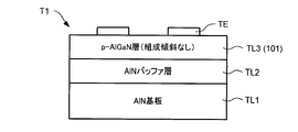
図6Aは、本実施例におけるコンタクト層15Bと同様に層内で異なる組成を有するp-AlGaN層と、比較例におけるコンタクト層101と同様に層内で一定の組成を有するp-AlGaN層と、におけるp電極17と同様の材料からなる金属層との間の接触抵抗の測定結果を示す図である。図6は、当該層内で一定の組成を有するp-AlGaN層と当該金属層との間の接触抵抗値を1とした場合の、当該層内で異なる組成を有するp-AlGaN層と当該金属層との間の接触抵抗値を示す図である。
FIG. 6A shows a p-AlGaN layer having a different composition in the layer like the contact layer 15B in the present example, and a p-AlGaN layer having a constant composition in the layer like the contact layer 101 in the comparative example. FIG. 6 is a diagram showing a measurement result of contact resistance between the p-electrode 17 and a metal layer made of the same material in FIG. FIG. 6 shows a p-AlGaN layer having a different composition in the layer and the metal having a contact resistance value of 1 between the p-AlGaN layer having a constant composition in the layer and the metal layer. It is a figure which shows the contact resistance value between layers.
なお、図6Aの結果を得るために、図6B及び図6Cに示すようなテスト構造T1及びT2を準備した。図6Bは、比較例におけるコンタクト層101と同様の組成を有するp-AlGaN層TL3を有するテスト構造T1の構成を示す図である。また、図6Cは、実施例におけるコンタクト層15Bと同様の組成を有するp-AlGaN層TL4を含むテスト構造T2の構成を示す図である。
Incidentally, in order to obtain the results of FIG. 6A, test structures T1 and T2 as shown in FIGS. 6B and 6C were prepared. FIG. 6B is a diagram showing the configuration of the test structure T1 including the p-AlGaN layer TL3 having the same composition as the contact layer 101 in the comparative example. FIG. 6C is a diagram showing the structure of the test structure T2 including the p-AlGaN layer TL4 having the same composition as the contact layer 15B in the example.
まず、図6Bに示すように、テスト構造T1は、AlN基板TL1上にAlNバッファ層TL2及びp-AlGaN層TL3が成長され、p-AlGaN層TL3上に金属層TEとしてNi層及びAu層が形成された構造を有する。また、図6Cに示すように、テスト構造T2は、AlN基板TL1上にAlNバッファ層TL2及びp-AlGaN層TL4が成長され、p-AlGaN層TL4上に金属層TEが形成された構造を有する。
First, as shown in FIG. 6B, in the test structure T1, the AlN buffer layer TL2 and the p-AlGaN layer TL3 are grown on the AlN substrate TL1, and the Ni layer and the Au layer are formed as the metal layer TE on the p-AlGaN layer TL3. It has a formed structure. Further, as shown in FIG. 6C, the test structure T2 has a structure in which the AlN buffer layer TL2 and the p-AlGaN layer TL4 are grown on the AlN substrate TL1, and the metal layer TE is formed on the p-AlGaN layer TL4. .
図6Aは、テスト構造T1におけるp-AlGaN層TL3と金属層TEとの間の接触抵抗と、テスト構造T2におけるp-AlGaN層TL4と金属層TEとの間の接触抵抗と、を測定した結果を示す図である。
FIG. 6A shows the measurement results of the contact resistance between the p-AlGaN layer TL3 and the metal layer TE in the test structure T1 and the contact resistance between the p-AlGaN layer TL4 and the metal layer TE in the test structure T2. FIG.
図6Aに示すように、層内で異なる組成を有するp-AlGaN層TL4においては、一定の組成を有するp-AlGaN層TL3に比べ、金属層TEとの間の接触抵抗が大幅に減少していることがわかる。
As shown in FIG. 6A, in the p-AlGaN layer TL4 having different compositions within the layer, the contact resistance with the metal layer TE is significantly reduced as compared with the p-AlGaN layer TL3 having a constant composition. You can see that
従って、層内で組成が異なるp-AlGaN層TL4と金属層TEとの間で良好なオーミックコンタクトを形成することができることがわかる。すなわち、コンタクト層15Bとp電極17とが良好なオーミックコンタクトを形成することができることがわかる。従って、コンタクト層15Bを形成することで、例えば、駆動電圧が低く、透光性の高いコンタクト層15Bを有する発光素子10を提供することができる。
Therefore, it can be seen that a good ohmic contact can be formed between the p-AlGaN layer TL4 and the metal layer TE having different compositions in the layer. That is, it can be seen that the contact layer 15B and the p electrode 17 can form a good ohmic contact. Therefore, by forming the contact layer 15B, it is possible to provide, for example, the light emitting element 10 having the contact layer 15B having a low driving voltage and high translucency.
なお、正孔の活性化率を増大させることを考慮すると、コンタクト層15Bは、歪を受けた状態で形成されていることが好ましい。すなわち、発光構造層であるn型半導体層12乃至p型半導体層15は、擬似格子整合した状態でエピタキシャル成長されていることが好ましい。従って、本実施例のように、n型半導体層12、活性層13、電子ブロック層14及びp型半導体層15は、成長用基板11としての単結晶のAlN基板上にエピタキシャル成長された半導体層であることが好ましい。また、同様に、コンタクト層15Bは、AlInGaNの組成を有することが好ましい。
In consideration of increasing the hole activation rate, the contact layer 15B is preferably formed in a strained state. That is, it is preferable that the n-type semiconductor layer 12 to the p-type semiconductor layer 15 which are the light emitting structure layers are epitaxially grown in a pseudo lattice-matched state. Therefore, as in this embodiment, the n-type semiconductor layer 12, the active layer 13, the electron block layer 14, and the p-type semiconductor layer 15 are semiconductor layers epitaxially grown on a single crystal AlN substrate as the growth substrate 11. Preferably there is. Similarly, the contact layer 15B preferably has a composition of AlInGaN.
また、より良好なオーミックコンタクトを形成することを考慮すると、コンタクト層15B(特にp電極17に接する界面の近傍)は、比較的高いドーパント濃度を有することが好ましい。例えば、コンタクト層15Bは、p型クラッド層15A以上のドーパント濃度を有することが好ましい。また、コンタクト層15Bは、p型クラッド層15Aよりも高いドーパント濃度を有していることが好ましい。
In consideration of forming a better ohmic contact, the contact layer 15B (particularly in the vicinity of the interface in contact with the p electrode 17) preferably has a relatively high dopant concentration. For example, the contact layer 15B preferably has a dopant concentration higher than that of the p-type cladding layer 15A. In addition, the contact layer 15B preferably has a higher dopant concentration than the p-type cladding layer 15A.
また、例えば、コンタクト層15Bは、p電極17との界面近傍、すなわちトンネルコンタクト層15BTにおいて最も高いドーパント濃度を有することが好ましい。この場合、コンタクト層15Bの全体がp型半導体層15Aよりも高いドーパント濃度を有している必要はない。
Further, for example, the contact layer 15B preferably has the highest dopant concentration in the vicinity of the interface with the p electrode 17, that is, in the tunnel contact layer 15BT. In this case, the entire contact layer 15B need not have a higher dopant concentration than the p-type semiconductor layer 15A.
例えば、コンタクト層15Bは、トンネルコンタクト層15BT以外の領域、例えばトンネルコンタクト層15BTよりもp型クラッド層15A側の領域において、p型クラッド層15A以下又は未満のドーパント濃度を有していてもよい。すなわち、例えば、コンタクト層15Bは、p電極17との界面近傍においてp型クラッド層15Aよりも高いドーパント濃度を有していることが好ましい。
For example, the contact layer 15B may have a dopant concentration equal to or lower than or equal to the p-type cladding layer 15A in a region other than the tunnel contact layer 15BT, for example, in a region closer to the p-type cladding layer 15A than the tunnel contact layer 15BT. . That is, for example, the contact layer 15B preferably has a higher dopant concentration than the p-type cladding layer 15A in the vicinity of the interface with the p-electrode 17.
図7は、発光素子10内における光の進路を模式的に示す図である。なお、図7においては、説明上、発光素子10内において活性層13からp型半導体層15に向かって放出された光(符号EL)の進路のみを示している。
FIG. 7 is a diagram schematically showing a path of light in the light emitting element 10. Note that, in FIG. 7, for the sake of explanation, only the path of light (reference numeral EL) emitted from the active layer 13 toward the p-type semiconductor layer 15 in the light emitting element 10 is shown.
本実施例においては、コンタクト層15BがAlGaNの組成を有する。また、コンタクト層15Bは、活性層13の井戸層13Aよりも大きなAl組成よりも大きなAl組成を有する。従って、コンタクト層15Bは、井戸層13Aよりも大きなバンドギャップを有する。
In this embodiment, the contact layer 15B has a composition of AlGaN. The contact layer 15B has an Al composition larger than that of the well layer 13A of the active layer 13. Therefore, the contact layer 15B has a larger bandgap than the well layer 13A.
従って、コンタクト層15Bは、活性層13から放出された光(符号EL)、すなわち井戸層13Aのバンドギャップに対応する波長の光(本実施例においては深紫外領域の光)に対して、ほとんど吸収性を有しない。従って、光(符号EL)の大部分は、コンタクト層15Bを透過する。また、本実施例においては、n型半導体層12、電子ブロック層14及びp型半導体層15の全体が活性層13からの放出光に対して透光性を有する。
Therefore, the contact layer 15B receives almost no light emitted from the active layer 13 (reference numeral EL), that is, light having a wavelength corresponding to the band gap of the well layer 13A (light in the deep ultraviolet region in this embodiment). It has no absorbency. Therefore, most of the light (code EL) is transmitted through the contact layer 15B. In addition, in this embodiment, the n-type semiconductor layer 12, the electron block layer 14, and the p-type semiconductor layer 15 are entirely transparent to the light emitted from the active layer 13.
また、本実施例においては、p電極17は、活性層13から放出された光に対して反射性を有する。従って、p型半導体層15を透過した光(符号EL)は、p電極17によって、n型半導体層12(成長用基板11)に向けて反射される。また、本実施例においては、成長用基板11は、AlNの組成を有する。従って、活性層13から放出された光の大部分は、発光素子10内で吸収されることなく、成長用基板11を介して外部に取り出される。
Further, in the present embodiment, the p-electrode 17 has reflectivity for the light emitted from the active layer 13. Therefore, the light (reference numeral EL) transmitted through the p-type semiconductor layer 15 is reflected by the p-electrode 17 toward the n-type semiconductor layer 12 (growth substrate 11). Further, in this embodiment, the growth substrate 11 has a composition of AlN. Therefore, most of the light emitted from the active layer 13 is extracted outside through the growth substrate 11 without being absorbed in the light emitting element 10.
すなわち、本実施例においては、成長用基板11のn型半導体層12とは反対側の表面は、発光素子10における光取り出し面として機能する。そして、この光取り出し面からは、高い効率で光が出射することとなる。
That is, in this embodiment, the surface of the growth substrate 11 opposite to the n-type semiconductor layer 12 functions as a light extraction surface of the light emitting element 10. Then, light is emitted from this light extraction surface with high efficiency.
上記したように、本実施例においては、発光素子10がp電極17との界面において組成が徐々に変化するコンタクト層15Bを有する。従って、発光構造層と電極とが良好なオーミックコンタクトを形成することができる。従って、駆動電圧の増加を抑制することができ、かつ光吸収の少ないコンタクト層15Bを形成することができる。
As described above, in this embodiment, the light emitting element 10 has the contact layer 15B whose composition gradually changes at the interface with the p-electrode 17. Therefore, a good ohmic contact can be formed between the light emitting structure layer and the electrode. Therefore, it is possible to suppress an increase in driving voltage and to form the contact layer 15B with less light absorption.
また、p電極17が反射性を有することによって、活性層13からの放出光を高効率で光取り出し面から取り出すことができる。従って、高い発光効率及び光取出し効率な発光素子10を提供することができる。
Further, since the p-electrode 17 has reflectivity, the emitted light from the active layer 13 can be extracted from the light extraction surface with high efficiency. Therefore, it is possible to provide the light emitting element 10 having high luminous efficiency and high light extraction efficiency.
なお、本実施例においては、p電極17は、良好なオーミックコンタクトを形成すること、及び高い反射性を有することが好ましい。従って、例えば、p電極17の材料としては、発光素子10の発光波長に対応するバンドギャップエネルギーと仕事関数との関係、並びに当該発光波長に対する反射性を考慮して選定すればよい。
In this example, it is preferable that the p-electrode 17 form a good ohmic contact and have high reflectivity. Therefore, for example, the material of the p electrode 17 may be selected in consideration of the relationship between the bandgap energy corresponding to the emission wavelength of the light emitting element 10 and the work function, and the reflectivity for the emission wavelength.
例えば、上記したように、p電極17の材料としては、Rh又はRuなどが挙げられる。また、p電極17の材料としては、当該発光波長への反射性を有する材料に限らず、極めて薄くすることで透光性を確保することができる電極材料であってもよい。例えば、p電極17は、ITOなどの金属酸化物並びにNi及びAuなどの金属上に、高い反射率を有するAlなどが積層された積層体であってもよい。
For example, as described above, examples of the material of the p-electrode 17 include Rh or Ru. Further, the material of the p-electrode 17 is not limited to a material having reflectivity for the emission wavelength, but may be an electrode material capable of ensuring translucency by making it extremely thin. For example, the p-electrode 17 may be a laminated body in which a metal oxide such as ITO and a metal such as Ni and Au are laminated with Al having a high reflectance.
このように、本実施例においては、発光素子10は、紫外領域に発光波長帯域を有し、p型半導体層15がp電極17との界面において組成が徐々に変化するコンタクト層15Bを有する。また、p電極17が当該紫外領域の光に対して反射性を有する。従って、高出力な発光素子10を提供することができる。
As described above, in the present embodiment, the light emitting element 10 has the emission wavelength band in the ultraviolet region, and the p-type semiconductor layer 15 has the contact layer 15B whose composition gradually changes at the interface with the p electrode 17. Further, the p electrode 17 has reflectivity for the light in the ultraviolet region. Therefore, it is possible to provide the light emitting device 10 with high output.
図8は、実施例2に係る発光素子20のバンド図である。発光素子20は、p型半導体層21の構成を除いては、発光素子10と同様の構成を有する。また、p型半導体層21は、コンタクト層21Aの構成を除いては、p型半導体層15と同様の構成を有する。
FIG. 8 is a band diagram of the light emitting element 20 according to the second embodiment. The light emitting element 20 has the same configuration as the light emitting element 10 except for the configuration of the p-type semiconductor layer 21. The p-type semiconductor layer 21 has the same structure as the p-type semiconductor layer 15 except for the structure of the contact layer 21A.
本実施例においては、コンタクト層21AにおけるAl組成yの減少率は、p型クラッド層15Aとの界面から、徐々に減少している。なお、コンタクト層21Aにおけるp型クラッド層15A側の組成及びp電極17側の組成は、コンタクト層15Bと同様である。従って、コンタクト層21Aは、図8に示すようなバンドギャップを示す。
In this embodiment, the reduction rate of Al composition y in the contact layer 21A gradually decreases from the interface with the p-type cladding layer 15A. The composition of the contact layer 21A on the p-type clad layer 15A side and the composition of the p-electrode 17 side are the same as those of the contact layer 15B. Therefore, the contact layer 21A exhibits a band gap as shown in FIG.
本実施例のように、p電極17との界面に向かって減少率を徐々に下げながらAl組成yを減少させることによっても、コンタクト層21A内における正孔の活性化率を増大させることができる。従って、p電極17との間で良好なオーミックコンタクトを形成することができる。従って、高出力な発光素子20を提供することができる。
The activation rate of holes in the contact layer 21A can also be increased by decreasing the Al composition y while gradually decreasing the reduction rate toward the interface with the p-electrode 17 as in the present embodiment. . Therefore, a good ohmic contact can be formed with the p electrode 17. Therefore, the light emitting element 20 with high output can be provided.
図9は、実施例3に係る発光素子30のバンド図である。発光素子30は、p型半導体層31の構成を除いては、発光素子10と同様の構成を有する。また、p型半導体層31は、コンタクト層31Aの構成を除いては、p型半導体層15と同様の構成を有する。
FIG. 9 is a band diagram of the light emitting element 30 according to the third embodiment. The light emitting element 30 has the same configuration as the light emitting element 10 except for the configuration of the p-type semiconductor layer 31. The p-type semiconductor layer 31 has the same structure as the p-type semiconductor layer 15 except for the structure of the contact layer 31A.
本実施例においては、コンタクト層31AにおけるAl組成yの減少率は、p型クラッド層15Aとの界面から、徐々に増加している。コンタクト層31Aにおけるp型クラッド層15A側の組成及びp電極17側の組成は、コンタクト層15Bと同様である。従って、コンタクト層31Aは、図9に示すようなバンドギャップを示す。
In this example, the decrease rate of Al composition y in the contact layer 31A gradually increases from the interface with the p-type cladding layer 15A. The composition of the contact layer 31A on the p-type clad layer 15A side and the composition of the p-electrode 17 side are the same as those of the contact layer 15B. Therefore, the contact layer 31A exhibits a band gap as shown in FIG.
本実施例のように、p電極17との界面に向かって減少率を徐々に上げながらAl組成yを減少させることによっても、コンタクト層31A内における正孔の活性化率を増大させることができる。従って、p電極17との間で良好なオーミックコンタクトを形成することができる。従って、高出力な発光素子30を提供することができる。
The activation rate of holes in the contact layer 31A can also be increased by decreasing the Al composition y while gradually increasing the decrease rate toward the interface with the p-electrode 17 as in the present embodiment. . Therefore, a good ohmic contact can be formed with the p electrode 17. Therefore, it is possible to provide the light emitting device 30 with high output.
上記した実施例2及び3のコンタクト層21A及び31Aのように、コンタクト層15Aは、変化率が変化しつつ、徐々にAl組成yが減少するように構成されていてもよい。このようにコンタクト層15Bを構成しても、p電極17との界面にトンネルコンタクト層15BTと同様なトンネルコンタクト層が形成される。従って、p型半導体層15、21及び31とp電極17と間で良好なオーミックコンタクトが形成される。従って、高出力な発光素子10、20及び30を提供することができる。
Like the contact layers 21A and 31A of Examples 2 and 3 described above, the contact layer 15A may be configured so that the Al composition y gradually decreases while the change rate changes. Even if the contact layer 15B is configured in this way, a tunnel contact layer similar to the tunnel contact layer 15BT is formed at the interface with the p electrode 17. Therefore, a good ohmic contact is formed between the p-type semiconductor layers 15, 21 and 31 and the p-electrode 17. Therefore, it is possible to provide the light emitting devices 10, 20 and 30 with high output.
なお、上記した実施例は一例に過ぎない。例えば、コンタクト層15B、21A及び31Aは、その全体で活性層13の井戸層13Aよりも大きなAl組成y(すなわちバンドギャップ)を有する。しかし、コンタクト層15B、21A又は31Aは、部分的に井戸層13Aよりも小さなAl組成yを有していてもよい。例えば、コンタクト層15Bは、p電極17との界面の近傍では井戸層13Aよりも小さなAl組成yを有していてもよい。この場合でも、大部分の光はコンタクト層15Bを透過することとなり、高い光取出し効率を得ることができる。
Note that the above embodiment is only an example. For example, the contact layers 15B, 21A, and 31A have an Al composition y (that is, a band gap) larger than that of the well layer 13A of the active layer 13 as a whole. However, the contact layers 15B, 21A or 31A may partially have the Al composition y smaller than that of the well layer 13A. For example, the contact layer 15B may have an Al composition y smaller than that of the well layer 13A in the vicinity of the interface with the p electrode 17. Even in this case, most of the light is transmitted through the contact layer 15B, and high light extraction efficiency can be obtained.
また、上記においては、p型半導体層15、21及び31の各々がp型クラッド層15Aとして一定のAl組成uを有するAlGaN層を有する場合について説明した。しかし、p型半導体層15、21及び31の構成はこれに限定されない。
Further, in the above description, the case where each of the p-type semiconductor layers 15, 21 and 31 has an AlGaN layer having a constant Al composition u as the p-type cladding layer 15A has been described. However, the configuration of the p-type semiconductor layers 15, 21 and 31 is not limited to this.
例えば、p型クラッド層15Aは、Al組成uが徐々に変化するAlGaNの組成を有する組成傾斜層であってもよい。この場合、p型半導体層15の全体がクラッド層及びコンタクト層として機能することとなる。すなわち、p型半導体層15は、クラッド層としてのみ機能するp型クラッド層15Aを有していなくてもよい。
For example, the p-type cladding layer 15A may be a composition gradient layer having a composition of AlGaN in which the Al composition u changes gradually. In this case, the entire p-type semiconductor layer 15 functions as a clad layer and a contact layer. That is, the p-type semiconductor layer 15 may not have the p-type clad layer 15A that functions only as a clad layer.
なお、p型クラッド層15Aを形成する場合、コンタクト層15B、21A又は31AのAl組成yは、オーミックコンタクトを形成することを考慮すると、p型クラッド層15AのAl組成uよりも大きな変化率で変化していることが好ましい。
When forming the p-type cladding layer 15A, the Al composition y of the contact layer 15B, 21A, or 31A has a larger rate of change than the Al composition u of the p-type cladding layer 15A in consideration of forming an ohmic contact. It is preferably changed.
換言すれば、p型半導体層15、21又は31は、p電極17上に形成され、p電極17との界面に向かって徐々にAl組成yが小さくなるAlGaN層からなるコンタクト層15B、21又は31Aを有していればよい。また、コンタクト層15Bのように、コンタクト層15B、21A及び31Aは、p電極17に接触し、トンネル接合によってp電極17に接続されたトンネルコンタクト層15BTを有していればよい。
In other words, the p- type semiconductor layer 15, 21 or 31 is formed on the p-electrode 17, and the contact layer 15B, 21 or 21 is formed of an AlGaN layer whose Al composition y gradually decreases toward the interface with the p-electrode 17. It suffices to have 31A. Further, like the contact layer 15B, the contact layers 15B, 21A, and 31A may have the tunnel contact layer 15BT that is in contact with the p electrode 17 and is connected to the p electrode 17 by the tunnel junction.
なお、発光効率を安定して向上させることを考慮すると、p型クラッド層15Aが設けられていることが好ましい。例えば、p型半導体層15、21又は31は、コンタクト層15B、21A又は31Aよりも活性層13側に形成され、コンタクト層15B、21A又は31Aよりも高いドーパント濃度を有するp型クラッド層15Aを有することが好ましい。
Note that it is preferable that the p-type cladding layer 15A is provided in consideration of stably improving the light emission efficiency. For example, the p- type semiconductor layer 15, 21 or 31 is formed closer to the active layer 13 than the contact layer 15B, 21A or 31A, and has a p-type cladding layer 15A having a higher dopant concentration than the contact layer 15B, 21A or 31A. It is preferable to have.
しかし、コンタクト層15B、21A又は31Aは、p電極17との界面においては、p型クラッド層15Aよりも高いドーパント濃度を有していてもよい。この場合、コンタクト層15B、21A又は31Aのドーパント濃度は、例えば、それぞれの層内で(例えばp型クラッド層15Aに向かって)変化し、p電極17との界面近傍以外の領域ではp型クラッド層15A以下またはこれよりも小さくなっていてもよい。このように層内でドーパント濃度を変化させる場合であっても、p型クラッド層15Aは、コンタクト層15B、21A又は31Aよりも高いドーパント濃度を有していることが好ましい。
However, the contact layers 15B, 21A, or 31A may have a higher dopant concentration than the p-type cladding layer 15A at the interface with the p-electrode 17. In this case, the dopant concentration of the contact layers 15B, 21A, or 31A changes, for example, in each layer (for example, toward the p-type clad layer 15A), and in the region other than the vicinity of the interface with the p-electrode 17, the p-type clad layer is formed. It may be smaller or smaller than the layer 15A. Even when the dopant concentration is changed in the layer as described above, the p-type cladding layer 15A preferably has a higher dopant concentration than the contact layers 15B, 21A, or 31A.
また、上記においては、p型半導体層15、21及び31が電子ブロック層14上に形成されている場合について説明した。しかし、電子ブロック層14、すなわち電子ブロック層として機能する半導体層が設けられず、活性層13上にp型半導体層15、21又は31が形成されていてもよい。この場合、例えば、p型半導体層15、21又は31は、活性層13との界面近傍において、Gaを含んでいなくてもよい。すなわち、p型半導体層15、21又は31は、部分的にAlNの組成を有していてもよい。
Further, in the above description, the case where the p-type semiconductor layers 15, 21 and 31 are formed on the electron block layer 14 has been described. However, the electron block layer 14, that is, the semiconductor layer functioning as the electron block layer may not be provided, and the p- type semiconductor layer 15, 21 or 31 may be formed on the active layer 13. In this case, for example, the p- type semiconductor layer 15, 21 or 31 may not contain Ga near the interface with the active layer 13. That is, the p- type semiconductor layer 15, 21 or 31 may partially have a composition of AlN.
また、上記においては、コンタクト層15B、21A及び31AがAlGaNの組成を有する場合について説明した。しかし、コンタクト層15B、21A及び31Aの組成はこれに限定されない。
Further, in the above description, the case where the contact layers 15B, 21A and 31A have the composition of AlGaN has been described. However, the composition of the contact layers 15B, 21A and 31A is not limited to this.
例えば、コンタクト層15B、21A及び31Aは、p電極17との界面に向かって徐々にバンドギャップが小さくなるような組成を有していればよい。例えば、コンタクト層15B、21A又は31Aは、AlInGaNの組成を有してればよい。すなわち、コンタクト層15B、21A又は31Aは、Inを含んでいてもよい。この場合、Al及びInの組成を調節することで、コンタクト層15B、21A又は31A内におけるバンドギャップが調節されていればよい。
For example, the contact layers 15B, 21A and 31A may have a composition such that the band gap gradually decreases toward the interface with the p-electrode 17. For example, the contact layers 15B, 21A or 31A may have a composition of AlInGaN. That is, the contact layers 15B, 21A or 31A may contain In. In this case, the band gap in the contact layer 15B, 21A or 31A may be adjusted by adjusting the composition of Al and In.
例えば、コンタクト層15B、21A又は31Aは、p電極17との界面に向かってAl組成が徐々に小さくなり、かつIn組成が徐々に大きくなるAlInGaNから構成されていてもよい。また、例えば、コンタクト層15B、21A又は31Aは、p電極17との界面に向かってAl組成が徐々に小さくなるAlInGaNから構成されていてもよい。
For example, the contact layers 15B, 21A or 31A may be made of AlInGaN in which the Al composition gradually decreases toward the interface with the p-electrode 17 and the In composition gradually increases. Further, for example, the contact layers 15B, 21A or 31A may be made of AlInGaN whose Al composition gradually decreases toward the interface with the p-electrode 17.
このようにコンタクト層15B、21A及び31Aを構成した場合であっても、正孔の活性化率が増大し、空乏層が薄くなることが期待できる。従って、良好なオーミックコンタクトによって高効率な電流注入を行うことができ、高い発光効率な発光素子10、20又は30を得ることができる。
Even when the contact layers 15B, 21A, and 31A are configured in this way, it can be expected that the hole activation rate increases and the depletion layer becomes thin. Therefore, high-efficiency current injection can be performed with good ohmic contact, and the light-emitting element 10, 20 or 30 having high light-emission efficiency can be obtained.
換言すれば、p型半導体層15、21又は31は、AlN、AlGaN又はAlInGaNの組成を有していればよい。そして、コンタクト層15A、21A又は31Aは、AlGaN又はAlInGaNの組成を有していればよい。
In other words, the p- type semiconductor layer 15, 21 or 31 may have a composition of AlN, AlGaN or AlInGaN. The contact layers 15A, 21A or 31A may have a composition of AlGaN or AlInGaN.
また、上記においては、p電極17が活性層13からの放出光に対して反射性を有する場合について説明した。しかし、p電極17の構成はこれに限定されない。p電極17は、p型半導体層15、21又は31上に形成されていればよい。そして、p型半導体層15、21及び31がp電極17に接するコンタクト層15B、21A及び31Aを有していればよい。これによって、p型半導体層15、21及び31とp電極17との間で良好なオーミックコンタクトが形成され、またp電極17が活性層13からの放出光に対して反射性を持つことによって、高い発光効率を得ることができる。
Further, in the above description, the case where the p-electrode 17 has reflectivity for the light emitted from the active layer 13 has been described. However, the structure of the p-electrode 17 is not limited to this. The p-electrode 17 may be formed on the p- type semiconductor layer 15, 21 or 31. The p-type semiconductor layers 15, 21 and 31 may have the contact layers 15B, 21A and 31A in contact with the p-electrode 17. As a result, good ohmic contact is formed between the p-type semiconductor layers 15, 21 and 31 and the p-electrode 17, and the p-electrode 17 has reflectivity with respect to the light emitted from the active layer 13. High luminous efficiency can be obtained.
上記したように、例えば、発光素子10は、AlGaNの組成を有するn型半導体層12と、n型半導体層12上に形成され、AlGaN系半導体からなる活性層13と、活性層13上に形成され、AlN、AlGaN又はAlInGaNの組成を有するp型半導体層15と、p型半導体層15上に形成されたp電極17を有する。
As described above, for example, the light emitting element 10 is formed on the n-type semiconductor layer 12 having the composition of AlGaN, the active layer 13 formed on the n-type semiconductor layer 12, and the active layer 13 made of an AlGaN-based semiconductor, and the active layer 13. And has a p-type semiconductor layer 15 having a composition of AlN, AlGaN, or AlInGaN, and a p-electrode 17 formed on the p-type semiconductor layer 15.
また、p型半導体層15は、p電極17上に形成され、p電極17との界面に向かってバンドギャップが小さくなるAlGaN層又はAlInGaN層からなるコンタクト層15Bを有する。また、コンタクト層15Bは、p電極17に接触し、トンネル接合によってp電極17に接続されたトンネルコンタクト層15BTを有する。また、発光素子20及び30は、コンタクト層15と同様のコンタクト層21A及び31Aを有する。従って、高出力な紫外領域の発光素子10、20及び30を提供することができる。
Further, the p-type semiconductor layer 15 has a contact layer 15B formed on the p-electrode 17 and made of an AlGaN layer or an AlInGaN layer having a band gap that decreases toward the interface with the p-electrode 17. Further, the contact layer 15B has a tunnel contact layer 15BT which is in contact with the p electrode 17 and is connected to the p electrode 17 by a tunnel junction. Further, the light emitting elements 20 and 30 have contact layers 21A and 31A similar to the contact layer 15. Therefore, it is possible to provide the light emitting devices 10, 20 and 30 in the ultraviolet region with high output.
10、20、30 半導体発光素子
12 n型半導体層
13 活性層
15、21、31 p型半導体層
15B、21A、31A コンタクト層 10, 20, 30 Semiconductor light emitting element 12 n-type semiconductor layer 13 Active layers 15, 21, 31 p-type semiconductor layers 15B, 21A, 31A Contact layer
12 n型半導体層
13 活性層
15、21、31 p型半導体層
15B、21A、31A コンタクト層 10, 20, 30 Semiconductor light emitting element 12 n-
Claims (8)
- AlGaN又はAlInGaNの組成を有するn型半導体層と、
前記n型半導体層上に形成され、AlGaN系半導体又はAlInGaN系半導体からなる活性層と、
前記活性層上に形成され、AlN、AlGaN又はAlInGaNの組成を有するp型半導体層と、
前記p型半導体層上に形成されたp電極と、を有し、
前記p型半導体層は、前記p電極上に形成され、前記p電極との界面に向かってバンドギャップが小さくなるAlGaN層又はAlInGaN層からなるコンタクト層を有し、
前記コンタクト層は、前記p電極に接触し、トンネル接合によって前記p電極に接続されたトンネルコンタクト層を有することを特徴とする半導体発光素子。 An n-type semiconductor layer having a composition of AlGaN or AlInGaN;
An active layer formed on the n-type semiconductor layer and made of an AlGaN-based semiconductor or an AlInGaN-based semiconductor;
A p-type semiconductor layer formed on the active layer and having a composition of AlN, AlGaN, or AlInGaN;
A p-electrode formed on the p-type semiconductor layer,
The p-type semiconductor layer has a contact layer formed on the p-electrode and formed of an AlGaN layer or an AlInGaN layer having a band gap that decreases toward the interface with the p-electrode.
The semiconductor light emitting device, wherein the contact layer includes a tunnel contact layer that is in contact with the p electrode and is connected to the p electrode by a tunnel junction. - 前記p電極は、前記活性層から放出された光に対して反射性を有することを特徴とする請求項1に記載の半導体発光素子。 The semiconductor light emitting device according to claim 1, wherein the p-electrode has reflectivity for light emitted from the active layer.
- 前記活性層は、井戸層及び前記井戸層よりも大きなバンドギャップの障壁層を含む量子井戸構造を有し、
前記p型半導体層は、前記井戸層よりも大きなバンドギャップを有することを特徴とする請求項1又は2に記載の半導体発光素子。 The active layer has a quantum well structure including a well layer and a barrier layer having a bandgap larger than that of the well layer,
The semiconductor light emitting device according to claim 1 or 2, wherein the p-type semiconductor layer has a bandgap larger than that of the well layer. - 前記n型半導体層、前記活性層及び前記p型半導体層は、単結晶のAlN基板上にエピタキシャル成長された半導体層であることを特徴とする請求項1又は2に記載の半導体発光素子。 The semiconductor light emitting device according to claim 1 or 2, wherein the n-type semiconductor layer, the active layer and the p-type semiconductor layer are semiconductor layers epitaxially grown on a single crystal AlN substrate.
- 前記p型半導体層は、前記コンタクト層よりも前記活性層側に形成されたp型クラッド層を有し、
前記コンタクト層は、前記p電極との界面近傍において前記p型クラッド層よりも高いドーパント濃度を有することを特徴とする請求項1乃至4のいずれか1つに記載の半導体発光素子。 The p-type semiconductor layer has a p-type cladding layer formed closer to the active layer than the contact layer is,
The semiconductor light emitting device according to claim 1, wherein the contact layer has a dopant concentration higher than that of the p-type clad layer in the vicinity of the interface with the p-electrode. - 前記コンタクト層は、前記p電極との界面に向かってAl組成が小さくなるAlGaN層からなることを特徴とする請求項1乃至5のいずれか1つに記載の半導体発光素子。 The semiconductor light emitting device according to any one of claims 1 to 5, wherein the contact layer comprises an AlGaN layer whose Al composition decreases toward an interface with the p electrode.
- 前記コンタクト層における前記Al組成の減少率は、前記p電極との界面に向かって減少することを特徴とする請求項6に記載の半導体発光素子。 7. The semiconductor light emitting device according to claim 6, wherein a reduction rate of the Al composition in the contact layer decreases toward an interface with the p electrode.
- 前記コンタクト層における前記Al組成の減少率は、前記p電極との界面に向かって増加することを特徴とする請求項6に記載の半導体発光素子。 7. The semiconductor light emitting device according to claim 6, wherein a reduction rate of the Al composition in the contact layer increases toward an interface with the p electrode.
Priority Applications (3)
| Application Number | Priority Date | Filing Date | Title |
|---|---|---|---|
| CN201980068568.8A CN112868109A (en) | 2018-10-17 | 2019-10-07 | Semiconductor light emitting element |
| EP19874318.9A EP3869571A4 (en) | 2018-10-17 | 2019-10-07 | Semiconductor light-emitting element |
| US17/285,848 US20210288216A1 (en) | 2018-10-17 | 2019-10-07 | Semiconductor light-emitting element |
Applications Claiming Priority (2)
| Application Number | Priority Date | Filing Date | Title |
|---|---|---|---|
| JP2018-195599 | 2018-10-17 | ||
| JP2018195599A JP7262965B2 (en) | 2018-10-17 | 2018-10-17 | semiconductor light emitting device |
Publications (1)
| Publication Number | Publication Date |
|---|---|
| WO2020080159A1 true WO2020080159A1 (en) | 2020-04-23 |
Family
ID=70283903
Family Applications (1)
| Application Number | Title | Priority Date | Filing Date |
|---|---|---|---|
| PCT/JP2019/039454 WO2020080159A1 (en) | 2018-10-17 | 2019-10-07 | Semiconductor light-emitting element |
Country Status (5)
| Country | Link |
|---|---|
| US (1) | US20210288216A1 (en) |
| EP (1) | EP3869571A4 (en) |
| JP (1) | JP7262965B2 (en) |
| CN (1) | CN112868109A (en) |
| WO (1) | WO2020080159A1 (en) |
Cited By (1)
| Publication number | Priority date | Publication date | Assignee | Title |
|---|---|---|---|---|
| JP7291357B1 (en) | 2022-02-24 | 2023-06-15 | 国立研究開発法人理化学研究所 | Ultraviolet light-emitting element and electrical equipment provided with the same |
Families Citing this family (4)
| Publication number | Priority date | Publication date | Assignee | Title |
|---|---|---|---|---|
| CN111628059B (en) * | 2020-04-28 | 2021-03-23 | 北京大学 | AlGaN-based deep ultraviolet light-emitting diode device and preparation method thereof |
| JP6867536B1 (en) * | 2020-07-07 | 2021-04-28 | 日機装株式会社 | Semiconductor light emitting device and manufacturing method of semiconductor light emitting device |
| CN115763666A (en) * | 2022-11-17 | 2023-03-07 | 马鞍山杰生半导体有限公司 | Ultraviolet light emitting diode chip |
| CN117637953A (en) * | 2024-01-25 | 2024-03-01 | 江西兆驰半导体有限公司 | LED epitaxial wafer, preparation method thereof and LED chip |
Citations (4)
| Publication number | Priority date | Publication date | Assignee | Title |
|---|---|---|---|---|
| JP2004266287A (en) * | 2004-04-06 | 2004-09-24 | Showa Denko Kk | Semiconductor device |
| JP2005033197A (en) * | 2003-06-20 | 2005-02-03 | Nichia Chem Ind Ltd | Nitride semiconductor device |
| JP2014086533A (en) * | 2012-10-23 | 2014-05-12 | Showa Denko Kk | Light-emitting diode and process of manufacturing the same |
| JP2016164966A (en) * | 2014-05-30 | 2016-09-08 | 三菱化学株式会社 | Nitride semiconductor wafer manufacturing method, nitride semiconductor wafer and nitride semiconductor chip |
Family Cites Families (8)
| Publication number | Priority date | Publication date | Assignee | Title |
|---|---|---|---|---|
| JP4207781B2 (en) * | 2002-01-28 | 2009-01-14 | 日亜化学工業株式会社 | Nitride semiconductor device having supporting substrate and method for manufacturing the same |
| US9401452B2 (en) * | 2012-09-14 | 2016-07-26 | Palo Alto Research Center Incorporated | P-side layers for short wavelength light emitters |
| CN103545405B (en) * | 2013-11-11 | 2016-03-30 | 天津三安光电有限公司 | Iii-nitride light emitting devices |
| CN105895757A (en) * | 2016-06-13 | 2016-08-24 | 湘能华磊光电股份有限公司 | LED epitaxial contact layer growing method |
| US10340415B2 (en) * | 2016-09-01 | 2019-07-02 | Lg Innotek Co., Ltd. | Semiconductor device and semiconductor device package including the same |
| KR102491456B1 (en) | 2017-03-27 | 2023-01-25 | 도와 일렉트로닉스 가부시키가이샤 | Group III nitride semiconductor light emitting device and manufacturing method thereof |
| US20180323338A1 (en) * | 2017-05-04 | 2018-11-08 | X Development Llc | Ultraviolet light emitting diode with tunnel junction |
| US20180331255A1 (en) * | 2017-05-12 | 2018-11-15 | X Development Llc | Fabrication of ultraviolet light emitting diode with tunnel junction |
-
2018
- 2018-10-17 JP JP2018195599A patent/JP7262965B2/en active Active
-
2019
- 2019-10-07 CN CN201980068568.8A patent/CN112868109A/en active Pending
- 2019-10-07 EP EP19874318.9A patent/EP3869571A4/en active Pending
- 2019-10-07 WO PCT/JP2019/039454 patent/WO2020080159A1/en unknown
- 2019-10-07 US US17/285,848 patent/US20210288216A1/en active Pending
Patent Citations (4)
| Publication number | Priority date | Publication date | Assignee | Title |
|---|---|---|---|---|
| JP2005033197A (en) * | 2003-06-20 | 2005-02-03 | Nichia Chem Ind Ltd | Nitride semiconductor device |
| JP2004266287A (en) * | 2004-04-06 | 2004-09-24 | Showa Denko Kk | Semiconductor device |
| JP2014086533A (en) * | 2012-10-23 | 2014-05-12 | Showa Denko Kk | Light-emitting diode and process of manufacturing the same |
| JP2016164966A (en) * | 2014-05-30 | 2016-09-08 | 三菱化学株式会社 | Nitride semiconductor wafer manufacturing method, nitride semiconductor wafer and nitride semiconductor chip |
Non-Patent Citations (1)
| Title |
|---|
| See also references of EP3869571A4 * |
Cited By (2)
| Publication number | Priority date | Publication date | Assignee | Title |
|---|---|---|---|---|
| JP7291357B1 (en) | 2022-02-24 | 2023-06-15 | 国立研究開発法人理化学研究所 | Ultraviolet light-emitting element and electrical equipment provided with the same |
| WO2023162839A1 (en) * | 2022-02-24 | 2023-08-31 | 国立研究開発法人理化学研究所 | Ultraviolet light-emitting element and electric device provided with same |
Also Published As
| Publication number | Publication date |
|---|---|
| CN112868109A (en) | 2021-05-28 |
| JP2020064955A (en) | 2020-04-23 |
| EP3869571A4 (en) | 2022-07-20 |
| EP3869571A1 (en) | 2021-08-25 |
| JP7262965B2 (en) | 2023-04-24 |
| US20210288216A1 (en) | 2021-09-16 |
Similar Documents
| Publication | Publication Date | Title |
|---|---|---|
| WO2020080159A1 (en) | Semiconductor light-emitting element | |
| JP4904261B2 (en) | Light emitting device having current blocking structure and method for manufacturing light emitting device having current blocking structure | |
| KR101855053B1 (en) | Nitride semiconductor ultraviolet light emitting element | |
| US9166098B2 (en) | Nitride semiconductor light emitting device | |
| KR101184862B1 (en) | Nitride semiconductor light emitting device, and method of fabricating nitride semiconductor light emitting device | |
| JP3863177B2 (en) | Gallium nitride light emitting device | |
| KR100947676B1 (en) | ?-nitride semiconductor light emitting device | |
| US20130228747A1 (en) | Nitride semiconductor light emitting device | |
| JP6924836B2 (en) | Optoelectronic semiconductor chip | |
| US20200350465A1 (en) | Semiconductor Heterostructure with P-type Superlattice | |
| KR101008588B1 (en) | ?-nitride compound semiconductor light emitting device | |
| JP2010087038A (en) | Light emitting element and lighting system | |
| KR101368687B1 (en) | Manufacturing Method of nitride semiconductor light emitting device using superlattice structure | |
| JP4493041B2 (en) | Nitride semiconductor light emitting device | |
| KR101333332B1 (en) | Light emitting diode and method of manufacturing the same | |
| JP2019186262A (en) | Nitride semiconductor light emitting element | |
| TWI776472B (en) | Semiconductor light-emitting element and method of manufacturing semiconductor light-emitting element | |
| JP2014003121A (en) | Nitride semiconductor light-emitting element | |
| JP7221593B2 (en) | semiconductor light emitting device | |
| KR20070079139A (en) | Method of manufacturing iii-nitride semiconductor template and iii-nitride semiconductor light emitting device and method for manufacturing the same | |
| JP2002151798A (en) | Nitride semiconductor element | |
| KR20100120102A (en) | Semiconductor light emitting device | |
| KR20130104822A (en) | Semiconductor light emitting device |
Legal Events
| Date | Code | Title | Description |
|---|---|---|---|
| 121 | Ep: the epo has been informed by wipo that ep was designated in this application |
Ref document number: 19874318 Country of ref document: EP Kind code of ref document: A1 |
|
| NENP | Non-entry into the national phase |
Ref country code: DE |
|
| ENP | Entry into the national phase |
Ref document number: 2019874318 Country of ref document: EP Effective date: 20210517 |