WO2020079970A1 - 半導体装置 - Google Patents
半導体装置 Download PDFInfo
- Publication number
- WO2020079970A1 WO2020079970A1 PCT/JP2019/034327 JP2019034327W WO2020079970A1 WO 2020079970 A1 WO2020079970 A1 WO 2020079970A1 JP 2019034327 W JP2019034327 W JP 2019034327W WO 2020079970 A1 WO2020079970 A1 WO 2020079970A1
- Authority
- WO
- WIPO (PCT)
- Prior art keywords
- semiconductor chip
- metal body
- terminal
- semiconductor
- semiconductor device
- Prior art date
- Legal status (The legal status is an assumption and is not a legal conclusion. Google has not performed a legal analysis and makes no representation as to the accuracy of the status listed.)
- Ceased
Links
Images







Classifications
-
- H—ELECTRICITY
- H10—SEMICONDUCTOR DEVICES; ELECTRIC SOLID-STATE DEVICES NOT OTHERWISE PROVIDED FOR
- H10W—GENERIC PACKAGES, INTERCONNECTIONS, CONNECTORS OR OTHER CONSTRUCTIONAL DETAILS OF DEVICES COVERED BY CLASS H10
- H10W90/00—Package configurations
-
- H—ELECTRICITY
- H10—SEMICONDUCTOR DEVICES; ELECTRIC SOLID-STATE DEVICES NOT OTHERWISE PROVIDED FOR
- H10W—GENERIC PACKAGES, INTERCONNECTIONS, CONNECTORS OR OTHER CONSTRUCTIONAL DETAILS OF DEVICES COVERED BY CLASS H10
- H10W72/00—Interconnections or connectors in packages
- H10W72/071—Connecting or disconnecting
- H10W72/073—Connecting or disconnecting of die-attach connectors
- H10W72/07351—Connecting or disconnecting of die-attach connectors characterised by changes in properties of the die-attach connectors during connecting
- H10W72/07354—Connecting or disconnecting of die-attach connectors characterised by changes in properties of the die-attach connectors during connecting changes in dispositions
-
- H—ELECTRICITY
- H10—SEMICONDUCTOR DEVICES; ELECTRIC SOLID-STATE DEVICES NOT OTHERWISE PROVIDED FOR
- H10W—GENERIC PACKAGES, INTERCONNECTIONS, CONNECTORS OR OTHER CONSTRUCTIONAL DETAILS OF DEVICES COVERED BY CLASS H10
- H10W72/00—Interconnections or connectors in packages
- H10W72/30—Die-attach connectors
- H10W72/341—Dispositions of die-attach connectors, e.g. layouts
- H10W72/347—Dispositions of multiple die-attach connectors
-
- H—ELECTRICITY
- H10—SEMICONDUCTOR DEVICES; ELECTRIC SOLID-STATE DEVICES NOT OTHERWISE PROVIDED FOR
- H10W—GENERIC PACKAGES, INTERCONNECTIONS, CONNECTORS OR OTHER CONSTRUCTIONAL DETAILS OF DEVICES COVERED BY CLASS H10
- H10W74/00—Encapsulations, e.g. protective coatings
-
- H—ELECTRICITY
- H10—SEMICONDUCTOR DEVICES; ELECTRIC SOLID-STATE DEVICES NOT OTHERWISE PROVIDED FOR
- H10W—GENERIC PACKAGES, INTERCONNECTIONS, CONNECTORS OR OTHER CONSTRUCTIONAL DETAILS OF DEVICES COVERED BY CLASS H10
- H10W90/00—Package configurations
- H10W90/701—Package configurations characterised by the relative positions of pads or connectors relative to package parts
- H10W90/731—Package configurations characterised by the relative positions of pads or connectors relative to package parts of die-attach connectors
- H10W90/736—Package configurations characterised by the relative positions of pads or connectors relative to package parts of die-attach connectors between a chip and a stacked lead frame, conducting package substrate or heat sink
Definitions
- the present disclosure relates to semiconductor devices.
- the semiconductor device described in Patent Document 1 includes, as semiconductor chips, a first semiconductor chip having a first element formed on a Si substrate and a second semiconductor chip having a second element formed on an SiC substrate.
- the first semiconductor chip and the second semiconductor chip are arranged in a region where the first metal body (first metal member) and the second metal body (second metal member) face each other, and are connected to the first metal body. Terminals are individually interposed between each semiconductor chip and the second metal body. In this way, the first element and the second element are connected in parallel between the first metal body and the second metal body.
- the Young's modulus of SiC that constitutes the second semiconductor chip is about three times as large as that of Si that constitutes the first semiconductor chip. Therefore, in the above structure in which the semiconductor chip is vertically sandwiched by the pair of metal bodies, thermal stress may cause cracks or the like in the bonding material on the second semiconductor chip side or the second semiconductor chip. That is, the reliability on the second semiconductor chip side using SiC may be lower than the reliability on the first semiconductor chip side using Si.
- the present disclosure aims to provide a semiconductor device that uses SiC and can improve the reliability on the second semiconductor chip side.
- a semiconductor device has one surface and a back surface opposite to the one surface as a surface forming an outer shell.
- the semiconductor device includes a first metal body arranged on one surface side, a second metal body arranged on the back surface side so as to face the first metal body, and a first metal body and a second metal body facing each other.
- first terminal interposed between the first semiconductor chip and a second terminal interposed between the first semiconductor chip and the second semiconductor chip.
- the linear expansion coefficient of the second terminal is smaller than the linear expansion coefficient of the first terminal in the direction orthogonal to the facing direction of the first metal body and the second metal body.
- the linear expansion coefficient of the second terminal is smaller than the linear expansion coefficient of the first terminal in the direction orthogonal to the facing direction. As a result, the thermal stress acting on the second semiconductor chip side can be reduced.
- the semiconductor device having such a configuration is sandwiched in the facing direction.
- a cooler is arranged on at least one of the one surface side and the back surface side, whereby the semiconductor device is cooled.
- the second total sum on the second semiconductor chip side is equal to or larger than the first total sum on the first semiconductor chip side. Therefore, even if each member expands due to the heat generation of the semiconductor chip, the semiconductor device is in close contact with the cooler on the second semiconductor chip side. Therefore, it is possible to suppress an increase in thermal resistance in the heat radiation path from the second semiconductor chip to the cooler while using the second terminal having a small linear expansion coefficient in the direction orthogonal to the facing direction. Therefore, it is possible to suppress the temperature rise of the second semiconductor chip and thereby reduce the thermal stress acting on the second semiconductor chip side.
- FIG. 1 is a diagram showing a schematic configuration of a power conversion device to which the semiconductor device of the first embodiment is applied
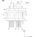
- FIG. 2 is a plan view showing a semiconductor device
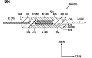
- 3 is a sectional view taken along the line III-III of FIG. 4 is a sectional view taken along line IV-IV of FIG.
- FIG. 5 is a plan view in which the sealing resin body is omitted
- FIG. 6 is a plan view showing the semiconductor device on the lower arm side.
- FIG. 7 is a plan view showing a laminated structure with a cooler
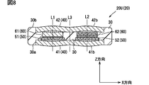
- FIG. 8 is a schematic diagram corresponding to FIG. 3, showing the semiconductor device when the element is heated.
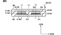
- FIG. 9 is a cross-sectional view showing a first modification and corresponding to FIG.
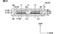
- FIG. 10 is a cross-sectional view showing a second modification and corresponding to FIG.
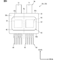
- FIG. 11 is a plan view showing the semiconductor device of the second embodiment
- 12 is a sectional view taken along line XII-XII of FIG.
- FIG. 13 is a plan view showing the semiconductor device on the lower arm side.
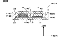
- FIG. 14 is a cross-sectional view showing another modification
- FIG. 15 is a sectional view showing another modification.
- the facing direction of the metal body is shown as the Z direction
- one direction orthogonal to the Z direction is shown as the X direction
- the direction orthogonal to both the Z direction and the X direction is referred to as the Y direction.
- the shape along the XY plane defined by the X direction and the Y direction described above is a planar shape.
- the power conversion device 10 shown in FIG. 1 is applicable to vehicles such as an electric vehicle (EV) and a hybrid vehicle (HV).
- the power conversion device 10 performs power conversion between the DC power supply 1 and the motor generator 2.
- the DC power supply 1 is a rechargeable secondary battery such as a lithium ion battery or a nickel hydrogen battery.
- the motor generator 2 is a three-phase AC type rotating electric machine.
- the motor generator 2 of this embodiment functions as a traveling drive source of the vehicle, that is, an electric motor. It also functions as a generator during regeneration.
- the motor generator 2 is not limited to the one that functions as a traveling drive source. It is also possible to employ a generator (alternator) that is driven by an engine (not shown) to generate electric power, and a device that functions as an electric motor (starter) that starts the engine.
- the power conversion device 10 includes at least a power conversion unit.
- the power converter 10 of this embodiment includes a smoothing capacitor 11, an inverter 12 as a power converter, a control circuit 13, and a drive IC 14.
- the smoothing capacitor 11 is connected between a P line 15 which is a high potential side power line and an N line 16 which is a low potential side power line.
- the P line 15 is connected to the positive electrode of the DC power supply 1
- the N line 16 is connected to the negative electrode of the DC power supply 1. Therefore, the N line 16 is also called a ground line.
- the smoothing capacitor 11 mainly smoothes the DC voltage supplied from the DC power supply 1.
- the inverter 12 is a DC-AC converter.
- the inverter 12 is configured to include upper and lower arm circuits 17 for three phases.
- the connection point of the U-phase upper and lower arm circuits 17 is connected to the U-phase winding provided on the stator of the motor generator 2.
- the connection point of the V-phase upper and lower arm circuits 17 is connected to the V-phase winding of the motor generator 2.
- the connection point of the W-phase upper and lower arm circuits 17 is connected to the W-phase winding of the motor generator 2.
- the connection point of the upper and lower arm circuits 17 is connected to the winding of the corresponding phase via the output line 18 provided for each phase.
- the output line 18, the P line 15 and the N line 16 described above are configured by a bus bar or the like.
- the upper and lower arm circuit 17 of each phase has an upper arm 17U and a lower arm 17L.
- the upper arm 17U and the lower arm 17L are connected in series between the P line 15 and the N line 16 with the upper arm 17U on the P line 15 side.
- Each arm, that is, each of the upper arm 17U and the lower arm 17L has switching elements Q1 and Q2 and a diode D1.
- the switching elements Q1 and Q2 are connected in parallel with each other.
- an n-channel type IGBT is adopted as the switching element Q1
- an n-channel type MOSFET is adopted as the switching element Q2.
- the diode D1 is connected in antiparallel to the IGBT, which is the switching element Q1, because of the return current.
- the collector electrode of the switching element Q1 and the drain electrode of the switching element Q2 are connected to the P line 15.
- the emitter electrode of the switching element Q1 and the source electrode of the switching element Q2 are connected to the N line 16.
- the emitter electrode of the switching element Q1 and the source electrode of the switching element Q2 in the upper arm 17U and the collector electrode of the switching element Q1 and the drain electrode of the switching element Q2 in the lower arm 17L are connected to each other and to the output line 18.
- the semiconductor device 20 described later constitutes one arm. That is, the two semiconductor devices 20 configure the upper and lower arm circuits 17, and the six semiconductor devices 20 configure the inverter 12.
- the inverter 12 converts the DC voltage into a three-phase AC voltage according to the switching control by the control circuit 13, and outputs it to the motor generator 2. As a result, the motor generator 2 is driven so as to generate a predetermined torque. Further, the inverter 12 converts the three-phase AC voltage generated by the motor generator 2 by receiving the rotational force from the wheels during regenerative braking of the vehicle into a DC voltage according to the switching control of the control circuit 13, and then to the P line 15. It can also be output. In this way, the inverter 12 performs bidirectional power conversion between the DC power supply 1 and the motor generator 2.
- the control circuit 13 generates a drive command for operating the switching elements Q1 and Q2 of the inverter 12, and outputs the drive command to the drive IC 14.
- the control circuit 13 generates a drive command based on a torque request input from a host ECU (not shown) and signals detected by various sensors.
- the various sensors include a current sensor that detects a phase current flowing in each phase winding of the motor generator 2, a rotation angle sensor that detects a rotation angle of a rotor of the motor generator 2, a voltage across the smoothing capacitor 11, that is, a P line. There is a voltage sensor for detecting the voltage of 15.
- the power conversion device 10 has these sensors (not shown). Specifically, the control circuit 13 outputs a PWM signal as a drive command.
- the control circuit 13 is configured to include, for example, a microcomputer.
- the drive IC 14 generates a drive signal based on the drive command from the control circuit 13.
- the drive IC 14 outputs the generated drive signal to the switching elements Q1 and Q2 of the corresponding arm.
- the gate electrodes of the switching elements Q1 and Q2 forming the same arm are electrically connected to the same drive IC 14.
- the drive IC 14 drives the switching elements Q1 and Q2 connected in parallel, that is, drives on and off.
- the drive IC 14 is also called a driver.
- the drive IC 14 is individually provided for each arm forming the inverter 12.
- the drive IC 14 may be provided for each of the upper and lower arm circuits 17, or may be provided integrally with the control circuit 13.
- the IGBT that is the switching element Q1 is formed on the Si substrate, and the MOSFET that is the switching element Q2 is formed on the SiC substrate.
- the control circuit 13 and the driving IC 14 are set so that only the SiC-MOSFET is turned on in the small current region and only the Si-IGBT or both the Si-IGBT and the SiC-MOSFET are turned on in the large current region. , Operate the inverter 12. Since the regions having excellent loss characteristics of the switching elements Q1 and Q2 connected in parallel are used, the loss can be reduced as a whole.
- the power conversion device 10 may further include a converter as a power conversion unit.
- the converter is a DC-DC converter that converts a DC voltage into a DC voltage having a different value.
- the converter is provided between the DC power supply 1 and the smoothing capacitor 11.
- the converter includes, for example, the upper and lower arm circuits 17 and the reactor described above. In this case, the upper and lower arm circuits 17 of the converter are also composed of the two semiconductor devices 20. Further, a filter capacitor for removing power supply noise from the DC power supply 1 may be further provided. The filter capacitor is provided between the DC power supply 1 and the converter.
- the semiconductor device 20 includes a sealing resin body 30, a metal body 40, a semiconductor chip 50, a terminal 60, a main terminal 70, a signal terminal 80, and a solder 90.
- the solder 90 corresponds to the joining material.
- the solder 90 has solders 91a, 91b, 91c used on the side of the first semiconductor chip 51, which will be described later, and solders 92a, 92b, 92c used on the side of the second semiconductor chip 52.
- the solders 91a, 91b, 91c correspond to the first bonding material
- the solders 92a, 92b, 92c correspond to the second bonding material.
- the sealing resin body 30 is made of, for example, an epoxy resin.
- the sealing resin body 30 is molded by, for example, a transfer molding method. As shown in FIGS. 2, 3, and 4, the sealing resin body 30 has one surface 30a and a back surface 30b opposite to the one surface 30a in the Z direction. The one surface 30a and the back surface 30b are flat surfaces, for example.
- the sealing resin body 30 has a side surface that connects the one surface 30a and the back surface 30b. In this embodiment, the sealing resin body 30 has a substantially rectangular shape in a plane.
- the metal body 40 functions to radiate the heat generated by the semiconductor chip 50 to the outside from the one surface 30a side or the back surface 30b side, for example.
- the metal body 40 electrically relays the semiconductor chip 50 and the main terminal 70, for example. That is, it functions as the wiring of the main electrode.
- the metal body 40 has both a heat dissipation function and a wiring function.
- the metal body 40 is formed by using at least a metal material having excellent electrical conductivity and thermal conductivity, such as Cu.
- a metal plate material, a wiring formed on a substrate (for example, a DBC substrate), or the like can be adopted.
- the metal bodies 40 are provided in pairs so as to sandwich the semiconductor chip 50.
- the metal body 40 has a first metal body 41 arranged on the one surface 30a side and a second metal body 42 arranged on the back surface 30b side.
- the first metal body 41 and the second metal body 42 face each other. This opposite direction is the Z direction. At least a part of the first metal body 41 and the second metal body 42 may face each other.
- the first metal body 41 has a mounting surface 41a that is a surface on the semiconductor chip 50 side and a heat dissipation surface 41b that is a surface opposite to the mounting surface 41a in the Z direction.
- the second metal body 42 has a mounting surface 42a that is a surface on the semiconductor chip 50 side and a heat dissipation surface 42b that is a surface opposite to the mounting surface 42a in the Z direction.
- the mounting surfaces 41a and 42a of the first metal body 41 and the second metal body 42 are opposed to each other.
- the first metal body 41 and the second metal body 42 are provided so as to substantially coincide with each other, that is, so as to substantially overlap with each other in the Z-direction projected view.
- Each metal body 40 has a flat plate shape with a substantially constant thickness, and is thicker than main terminals 70 and signal terminals 80 described later. Such a metal body 40 is also called a heat sink.
- Each metal body 40 has a shape in which four corners are cut out in a substantially rectangular plane shape having a long side in the X direction.
- the mounting surfaces 41a and 42a are surfaces that are substantially orthogonal to the Z direction, that is, surfaces that are substantially parallel to the XY plane.
- the heat dissipation surface 41b of the first metal body 41 is exposed from the sealing resin body 30.
- the heat dissipation surface 41b is substantially flush with the one surface 30a.
- a portion other than the connection portion with the solder 90, the heat radiation surface 41b, and the portion where the main terminal 70 is continuous is covered with the sealing resin body 30.
- most of the second metal body 42 is covered with the sealing resin body 30.
- the heat dissipation surface 42b of the second metal body 42 is exposed from the sealing resin body 30.
- the heat dissipation surface 42b is substantially flush with the back surface 30b.
- a portion of the surface of the second metal body 42 excluding a portion where the connection with the solder 90, the heat radiation surface 42b, and the main terminal 70 are continuous is covered with the sealing resin body 30.
- the outer surface of the semiconductor device 20 in the Z direction is configured by the one surface 30a and the heat dissipation surface 41b on one side and the back surface 30b and the heat dissipation surface 42b on the other side.
- the semiconductor chip 50 is formed by forming the above-mentioned elements forming the arm on a semiconductor substrate.
- the semiconductor device 20 includes a plurality of semiconductor chips 50.
- the plurality of semiconductor chips 50 are arranged side by side on the mounting surface 41 a of the first metal body 41 in the region where the first metal body 41 and the second metal body 42 face each other. Then, each semiconductor chip 50 is connected to the first metal body 41 via the solder 90.
- the semiconductor chip 50 is arranged so that its thickness direction is substantially parallel to the Z direction.
- the element has a vertical structure so that the main current flows in the Z direction. Therefore, the semiconductor chip 50 has main electrodes on both surfaces in the Z direction.
- the semiconductor chip 50 has a first semiconductor chip 51 having a first element formed on a Si substrate and a second semiconductor chip 52 having a second element formed on a SiC substrate.
- the semiconductor chip 50 has at least one of each of the first semiconductor chip 51 and the second semiconductor chip 52.
- each of the first semiconductor chip 51 and the second semiconductor chip 52 is provided.
- the alignment direction of the first semiconductor chip 51 and the second semiconductor chip 52 is substantially parallel to the X direction.
- a center line CL indicated by a chain double-dashed line in FIGS. 2 and 5 is an imaginary line that passes through the elemental center that is the center of the entire semiconductor chips 50 and is orthogonal to the thickness direction and the arrangement direction of the semiconductor chips 50.
- the center line CL of the present embodiment passes through the center position between the center of the first semiconductor chip 51 and the center of the second semiconductor chip 52.
- the opposing region of the metal body 40 has a symmetry that is bisected by the center line CL described above.
- the first semiconductor chip 51 is arranged in the first region of the facing region of the metal body 40 that is bisected in the X direction by the center line CL, and the second semiconductor region is formed in the second region different from the first region.
- a semiconductor chip 52 is arranged.
- the switching element Q1, that is, the IGBT, and the diode D1 are integrally formed. That is, an RC (Reverse Conducting) -IGBT is formed as the first element.
- the switching element Q2 described above, that is, the MOSFET is formed as a second element.
- each element has a gate electrode.
- the gate electrode has a trench structure.
- the first semiconductor chip 51 has a collector electrode 51c as a main electrode on the surface on the first metal body 41 side, and an emitter electrode 51e as a main electrode on the surface on the second metal body 42 side.
- the collector electrode 51c also serves as the cathode electrode of the diode D1, and the emitter electrode 51e also serves as the anode electrode of the diode D1.
- the collector electrode 51c is formed on almost the entire surface, and the emitter electrode 51e is formed on a part of the surface.
- the collector electrode 51c of the first semiconductor chip 51 is connected to the mounting surface 41a of the first metal body 41 via the solder 91a.
- the second semiconductor chip 52 has a drain electrode 52d as a main electrode on the surface on the first metal body 41 side and a source electrode 52s as a main electrode on the surface on the second metal body 42 side.
- the drain electrode 52d is formed on almost the entire surface, and the source electrode 52s is formed on a part of the surface.
- the drain electrode 52d of the second semiconductor chip 52 is connected to the mounting surface 41a of the first metal body 41 via the solder 92a.
- the first semiconductor chip 51 has a pad 51p which is a signal electrode on the emitter electrode formation surface.
- the pad 51p is formed at a position different from the emitter electrode 51e, and is electrically separated from the emitter electrode 51e.
- the pad 51p is formed at the end portion on the side opposite to the formation region of the emitter electrode 51e in the Y direction.
- the second semiconductor chip 52 has a pad 52p on the source electrode formation surface.
- the pad 52p is formed at a position different from the source electrode 52s, and is electrically separated from the source electrode 52s.
- the pad 52p is formed at the end portion on the side opposite to the formation region of the source electrode 52s in the Y direction. In the Y direction, the emitter electrode 51e and the source electrode 52s are formed on the same side, and the pads 51p and 52p are formed on the same side.
- the first semiconductor chip 51 has five pads 51p.
- the five pads 51p are for the gate electrode, for detecting the potential of the emitter electrode 51e, for sensing current, for the anode potential of a temperature sensor (temperature sensitive diode) that detects the temperature of the first semiconductor chip 51, and It has a cathode potential.
- the plurality of pads 51p are collectively formed on one end side in the Y direction of the first semiconductor chip 51 having a substantially rectangular plane shape, and are formed side by side in the X direction.
- the second semiconductor chip 52 has five pads 52p.
- the five pads 52p are for the gate electrode, the potential detection of the source electrode 52s, the current sense, the anode potential of the temperature sensor (temperature sensitive diode) for detecting the temperature of the second semiconductor chip 52, and the same. It has a cathode potential.
- the plurality of pads 52p are collectively formed on one end side in the Y direction of the second semiconductor chip 52 having a substantially rectangular plane shape, and are formed side by side in the X direction.
- the terminal 60 is interposed between the second metal body 42 and the semiconductor chip 50 so as to secure a predetermined distance between the second metal body 42 and the semiconductor chip 50.
- the thickness of the terminal 60 is made sufficiently longer than the thickness of the semiconductor chip 50.
- the terminal 60 has a heat transfer function in the heat dissipation path from the semiconductor chip 50 to the second metal body 42.
- the terminal 60 has an electrical relay function in an electric conduction path from the semiconductor chip 50 to the second metal body 42.
- the terminal 60 is formed using a metal material.
- the terminal 60 is also called a metal block or a metal spacer.
- the terminals 60 are individually provided for each semiconductor chip 50, and the semiconductor device 20 has the same number as the semiconductor chips 50, that is, a plurality of terminals 60.
- the terminal 60 has a first terminal 61 arranged on the first semiconductor chip 51 side and a second terminal 62 arranged on the second semiconductor chip 52 side.
- the terminal 60 secures a predetermined distance between the second metal body 42 and the semiconductor chip 50 so that the bonding wire 93 described later does not contact the mounting surface 42a of the second metal body 42.
- each terminal 60 has a substantially rectangular parallelepiped shape.
- the planar shape of the first terminal 61 is substantially the same as the emitter electrode 51e
- the planar shape of the second terminal 62 is substantially the same as the source electrode 52s.
- One surface in the Z direction of the first terminal 61 is connected to the emitter electrode 51e of the first semiconductor chip 51 via the solder 91b, and the back surface opposite to the one surface is a mounting surface of the second metal body 42 via the solder 91c. It is connected to 42a.
- One surface in the Z direction of the second terminal 62 is connected to the source electrode 52s of the second semiconductor chip 52 via the solder 92b, and the back surface opposite to the one surface is a mounting surface of the second metal body 42 via the solder 92c. It is connected to 42a. Details of the terminal 60 will be described later.
- the main terminal 70 is a terminal through which a main current flows among the external connection terminals for electrically connecting the semiconductor device 20 and an external device.
- the semiconductor device 20 includes a plurality of main terminals 70.
- the main terminal 70 is connected to the corresponding metal body 40.
- the main terminal 70 may be integrally provided with the corresponding metal body 40 by processing the same metal member, or the main terminal 70, which is a separate member, may be connected to the metal body 40 by connection.
- the main terminal 70 is connected to the corresponding metal body 40 inside the sealing resin body 30.
- each of the main terminals 70 is extended from the corresponding metal body 40 in the Y direction and protrudes from one side surface 30c of the sealing resin body 30 to the outside.
- the main terminal 70 extends inside and outside the sealing resin body 30.
- the main terminal 70 is a terminal electrically connected to the main electrode on the first metal body 41 side of the semiconductor chip 50.
- the semiconductor device 20 has, as the main terminals 70, a first main terminal 71 electrically connected to the collector electrode 51c and the drain electrode 52d, and a second main terminal 72 electrically connected to the emitter electrode 51e and the source electrode 52s. have.
- the first main terminal 71 is connected to the first metal body 41, and extends in the Y direction from the side surface of the first metal body 41 near the side surface 30c.
- the second main terminal 72 is connected to the second metal body 42 and extends in the Y direction from the side surface of the second metal body 42 near the side surface 30c.
- the first main terminal 71 is provided integrally with the first metal body 41 by processing the same metal plate.
- the second main terminal 72 is provided integrally with the second metal body 42 by processing the same metal plate.
- Both the first main terminal 71 and the second main terminal 72 have a bent portion in the sealing resin body 30 and project from substantially the same position in the Z direction on the side surface 30c.
- the protruding portion of the first main terminal 71 and the protruding portion of the second main terminal 72 are arranged side by side in the X direction with a predetermined gap so that the side surfaces face each other.
- the first main terminal 71 is arranged on the first semiconductor chip 51 side and the second main terminal 72 is arranged on the second semiconductor chip 52 side with respect to the center line CL.
- the signal terminal 80 is connected to the pad of the corresponding semiconductor chip 50.
- the signal terminal 80 has a first signal terminal 81 connected to the pad 51p of the first semiconductor chip 51 and a second signal terminal 82 connected to the pad 52p of the second semiconductor chip 52.
- the first signal terminal 81 and the second signal terminal 82 are connected to the corresponding pads 51p and 52p via the bonding wire 93.
- the signal terminal 80 is connected to the bonding wire 93 inside the sealing resin body 30.
- Each of the signal terminals 80 extends in the Y direction, and projects outward from a side surface 30d of the sealing resin body 30 opposite to the side surface 30c.
- the signal terminal 80 is provided as a part of a lead frame including the first main terminal 71 and the first metal body 41.
- the sealing resin body 30 partially covers each of the metal bodies 40, each of the semiconductor chips 50, the terminals 60, each of the main terminals 70, and each of the signal terminals 80. However, they are integrally sealed. That is, the elements constituting one arm are sealed. Therefore, the semiconductor device 20 is also called a 1-in-1 package.
- the heat dissipation surface 41b of the first metal body 41 is substantially flush with the one surface 30a of the sealing resin body 30.
- the heat dissipation surface 42b of the second metal body 42 is substantially flush with the back surface 30b of the sealing resin body 30.
- the semiconductor device 20 has a double-sided heat dissipation structure in which both heat dissipation surfaces 41b and 42b are exposed from the sealing resin body 30.
- Such a semiconductor device 20 can be formed, for example, by cutting the metal body 40 together with the sealing resin body 30.
- the heat radiation surfaces 41b and 42b may be formed by molding the sealing resin body 30 such that the heat radiation surfaces 41b and 42b come into contact with the cavity wall surface of the mold for molding the sealing resin body 30.
- the above semiconductor device 20 may be a common component for the upper arm 17U and the lower arm 17L. According to this, the number of parts can be reduced.
- the semiconductor device 20 described above is used as the semiconductor device 20U for the upper arm 17U.
- FIG. 6 shows a semiconductor device 20L for the lower arm 17L.
- the first main terminal 71 is arranged on the second semiconductor chip 52 side and the second main terminal 72 is arranged on the first semiconductor chip 51 side with respect to the center line CL described above.
- the other configuration is the same as that of the semiconductor device 20U (see FIG. 2) on the side of the upper arm 17U. 2 to 6 show the state at room temperature.
- the semiconductor device 20 described above is alternately stacked with the cooler 100, as shown in FIG. 7.
- the semiconductor device 20 constitutes a power module 110 together with the cooler 100.
- the cooler 100 has a refrigerant flow path inside.
- the coolers 100 are arranged in multiple stages at predetermined intervals in the Z direction.
- the multi-stage cooler 100 is connected by a supply pipe 101 on one end side in the X direction.
- the supply pipe 101 is a tubular body having a flow path formed therein, and extends in the Z direction.
- the supply pipe 101 is connected to each of the coolers 100, and the flow path of the supply pipe 101 communicates with the flow path of each of the coolers 100.
- the multi-stage cooler 100 is connected by a discharge pipe 102 on the end side opposite to the supply pipe 101.
- the discharge pipe 102 is also a tubular body having a flow passage formed therein, and extends in the Z direction.
- the discharge pipe 102 is connected to each of the coolers 100, and the flow path of the discharge pipe 102 communicates with the flow path of each of the coolers 100.
- the refrigerant that has flowed in from the supply pipe 101 expands the flow path of each cooler 100 and is discharged from the discharge pipe 102.
- An inner fin (not shown) may be arranged in the flow path of the cooler 100.
- the inner fin is a metal plate bent in a wave shape. The arrangement of the inner fins can promote heat transfer between the cooler 100 and the refrigerant.
- a phase change refrigerant such as water or ammonia, or a phase change refrigerant such as ethylene glycol
- the cooler 100 mainly cools the semiconductor device 20. However, in addition to the cooling function, it may have a function of warming when the environmental temperature is low. In this case, the cooler 100 is called a temperature controller.
- the refrigerant is also called a heat medium.
- the power module 110 includes six semiconductor devices 20 that form the inverter 12, and a plurality of (multi-stage) coolers 100 that are alternately stacked with the semiconductor devices 20 so as to cool each of the semiconductor devices 20 from both sides. ing.
- the semiconductor device 20 is sandwiched by the coolers 100 from both sides in the Z direction.
- Most of the sealing resin body 30 is arranged in the facing region of the adjacent coolers 100.
- Each of the main terminals 70 is extended to the outside of the facing region in the Y direction, for example, for connection with a bus bar or the like not shown.
- the respective semiconductor devices 20 are arranged so as to overlap each other when viewed in the Z direction.
- the semiconductor device 20 is arranged such that the second semiconductor chip 52 using SiC is on the upstream side and the first semiconductor chip 51 using Si is on the downstream side. That is, in the X direction, the second semiconductor chip 52 is arranged on the supply pipe 101 side and the first semiconductor chip 51 is arranged on the discharge pipe 102 side. Thereby, the second semiconductor chip 52 can be effectively cooled.
- the semiconductor device 20U for the upper arm 17U and the semiconductor device 20L for the lower arm 17L that configure each phase of the inverter 12 are arranged so as to be adjacent to each other in the Z direction.
- the second main terminal 72 of the semiconductor device 20U and the first main terminal 71 of the semiconductor device 20L, which are in the same phase, are arranged so as to overlap each other when viewed in the Z direction. Therefore, the connection distance between the upper arm 17U and the lower arm 17L can be shortened. Also, the connectivity can be improved.
- the semiconductor device 20 (20U, 20L) is cooled by the cooler 100 while being sandwiched in the Z direction, which is the facing direction.
- the configurations of the first terminal 61 and the second terminal 62 are different. That is, different metal members are used for the first terminal 61 and the second terminal 62.
- the linear expansion coefficient of the second terminal 62 is smaller than the linear expansion coefficient of the first terminal 61 in the direction orthogonal to the Z direction, that is, the direction parallel to the XY plane. Further, the coefficient of linear expansion of the second terminal 62 is smaller than that in the Z direction in the direction orthogonal to the Z direction. As described above, the second terminal 62 has the anisotropy of the linear expansion coefficient.
- the second terminal 62 for example, as shown in FIG. 3, a clad material in which a plurality of types of metal layers are stacked and adjacent layers are joined together can be used.
- a CuMo clad material in which Cu layers and Mo layers are alternately stacked in the Z direction is used as the second terminal 62. Further, Cu is used as the first terminal 61.
- the linear expansion coefficient of Cu forming the first terminal 61 is about 17 ⁇ 10 ⁇ 6 / K.
- the linear expansion coefficient of the second terminal 62 is substantially equal to that of Cu in the Z direction, and is 6 to 10 ⁇ 10 ⁇ 6 / K in the direction orthogonal to the Z direction.
- the first virtual line L1 is a virtual line that is parallel to the Z direction and passes through a region that overlaps with the first terminal 61 in the Z direction projection view, in other words, a region that overlaps with the emitter electrode 51e.
- the second virtual line L2 is a virtual line that is parallel to the Z direction and passes through a region overlapping with the second terminal 62 in the Z direction projection view, in other words, a region overlapping with the source electrode 52s.
- the third imaginary line L3 is parallel to the Z direction, does not overlap with the semiconductor chip 50, the terminal 60, and the solder 90 when viewed in the Z direction, and does not overlap the first metal body 41, the second metal body 42, and the sealing. It is an imaginary line that passes through a region overlapping the resin body 30. That is, the first virtual line L1, the second virtual line L2, and the third virtual line L3 are parallel to the facing direction.
- the first virtual line L1 passes through the first metal body 41, the solder 91a, the first semiconductor chip 51, the solder 91b, the first terminal 61, the solder 91c, and the second metal body 42.
- the above-mentioned respective elements through which the first virtual line L1 passes are members arranged on the first virtual line L1 from one surface to the back surface of the semiconductor device 20.
- the second virtual line L2 passes through the first metal body 41, the solder 92a, the second semiconductor chip 52, the solder 92b, the second terminal 62, the solder 92c, and the second metal body 42.
- the above-described respective elements through which the second virtual line L2 passes are members arranged on the second virtual line L2 from one surface to the back surface of the semiconductor device 20.
- the first virtual line L1 passes through the center of the emitter electrode 51e of the first semiconductor chip 51
- the second virtual line L2 passes through the center of the source electrode 52s of the second semiconductor chip 52.
- the third virtual line L3 passes through the first metal body 41, the sealing resin body 30, and the second metal body 42.
- the above-described respective elements through which the third virtual line L3 passes are members arranged on the third virtual line L3 from one surface to the back surface of the semiconductor device 20.
- the third virtual line L3 is located at an intermediate position between the above-mentioned emitter center of the first semiconductor chip 51 and the above-mentioned source center of the second semiconductor chip 52 in the X direction which is the arrangement direction of the semiconductor chips 50. Pass through.
- the first sum S1 is the sum of the products of the thickness of each member and the coefficient of linear expansion in the Z direction on the first imaginary line L1, that is, the sum.
- the second sum S2 is the sum of the product of the thickness of each member and the coefficient of linear expansion in the Z direction on each of the members on the second virtual line L2.
- the third total sum S3 is the total sum of the product of the thickness of each member and the linear expansion coefficient in the Z direction on each of the members on the third virtual line L3.
- the third sum S3 is the product of the thickness and the linear expansion coefficient of the first metal body 41 and the product of the thickness and the linear expansion coefficient of the sealing resin body 30 between the metal bodies 40 on the third virtual line L3. It is the sum of the product of the thickness and the linear expansion coefficient of the second metal body 42.
- the semiconductor device 20 is configured such that the second total sum S2 on the SiC side is equal to or larger than the first total sum S1 on the Si side.
- the semiconductor device 20 satisfies the relationship of S2 ⁇ S1 at least within the temperature range in which the semiconductor device 20 (semiconductor chip 50) is cooled.
- the above relationship is satisfied in a predetermined temperature range including room temperature, specifically, in the range of 0 ° C. to maximum junction temperature Tjmax (eg 150 ° C.).
- Tjmax maximum junction temperature
- the above relationship may be satisfied in the entire operating temperature range of the vehicle (for example, ⁇ 40 ° C. to 150 ° C.).
- the linear expansion coefficients of the first semiconductor chip 51 using Si and the second semiconductor chip 52 using SiC are set to about 4 ⁇ 10 ⁇ 6 / K, respectively.
- the semiconductor chips 52 have almost the same thickness.
- the coefficient of linear expansion of the second terminal 62 is substantially equal to that of the first terminal 61 in the Z direction, and the thicknesses of the first terminal 61 and the second terminal 62 are substantially equal.
- the first metal body 41 has a flat plate shape with a substantially constant thickness
- the second metal body 42 also has a flat plate shape with a substantially constant thickness.
- the same material is used as the solder 90, and the linear expansion coefficients are made equal to each other.
- the sum of the thicknesses of the solders 91a, 91b, 91c is made substantially equal to the sum of the thicknesses of the solders 92a, 92b, 92c.
- the second total sum S2 shows a value substantially equal to the first total sum S1. Further, even when the element generates heat (for example, 100 ° C.), the second total sum S2 shows a value almost equal to the first total sum S1.
- the semiconductor device 20 is configured such that the third total sum S3 is equal to or less than the first total sum S1 on the Si side. That is, the semiconductor device 20 is configured so as to satisfy S2 ⁇ S1 ⁇ S3. The semiconductor device 20 satisfies the relationship of S3 ⁇ S1 within the above-mentioned predetermined temperature range.
- the first metal body 41 has a flat plate shape with a substantially constant thickness
- the second metal body 42 also has a flat plate shape with a substantially constant thickness.
- the coefficient of linear expansion of the sealing resin body 30 is larger than that of the semiconductor chip 50 and smaller than that of the metal body 40. Specifically, it is adjusted to fall within the range of 6 to 14 ⁇ 10 ⁇ 6 / K. That is, the value is smaller than that of the terminal 60 in the Z direction.
- the third total sum S3 shows a value substantially equal to the first total sum S1.
- the element generates heat (for example, 100 ° C.)
- the third total sum S3 shows a value smaller than the first total sum S1.
- the linear expansion coefficient of the second terminal 62 is smaller than the linear expansion coefficient of the first terminal 61 in the direction orthogonal to the Z direction.
- the coefficient of linear expansion of the second terminal 62 is close to the coefficient of linear expansion of the second semiconductor chip 52 in the direction orthogonal to the Z direction. Therefore, it is possible to reduce the thermal stress that acts on the SiC-side solders 92a, 92b, 92c and the second semiconductor chip 52 based on the difference in linear expansion coefficient in the direction orthogonal to the Z direction. In particular, the thermal stress acting on the solder 92b between the second semiconductor chip 52 and the second terminal 62 can be effectively reduced.
- the reliability on the second semiconductor chip 52 side is improved. It is possible to prevent the reliability of the first semiconductor chip 51 side from being deteriorated.
- the reliability target on the second semiconductor chip 52 side is the second semiconductor chip 52 and the solders 92a, 92b, 92c.
- the target of reliability on the first semiconductor chip 51 side is the first semiconductor chip 51 and the solders 91a, 91b, 91c.
- the semiconductor device 20 is sandwiched by the cooler 100 from both sides in the Z direction.
- the second sum S2 on the second semiconductor chip 52 side is set to be equal to or larger than the first sum S1 on the first semiconductor chip 51 side.
- the semiconductor device 20 satisfies the relationship of S2 ⁇ S1. Therefore, in the temperature range where the semiconductor chip 50 needs to be cooled, the portion of the semiconductor device 20 on the second semiconductor chip 52 side can be brought into close contact with the cooler 100.
- FIG. 8 is a schematic diagram showing the semiconductor device 20 during element heat generation, and corresponds to FIG. 3.
- the linear expansion coefficient of the second terminal 62 is made smaller in the direction orthogonal to the Z direction than in the Z direction. In this way, if the second semiconductor chip 52 has anisotropy that easily expands in the Z direction, the second semiconductor chip 52 side can be easily attached to the cooler 100 when the second semiconductor chip 52 generates heat. As a result, it is possible to effectively cool the second semiconductor chip 52, which has a higher Young's modulus and is desired to reduce thermal stress.
- the thickness of the terminal 60 is, for example, about 1 mm, which is sufficiently thick with respect to other elements between the metal bodies 40 on the virtual lines L1 and L2. Another factor is the thickness on the order of um.
- the first terminal 61 and the second terminal 62 have substantially the same linear expansion coefficient in the Z direction and the thickness. Therefore, the thickness of the terminal 60 when expanded is substantially equal on the Si side and the SiC side. Therefore, the increase in thermal resistance can be suppressed also on the first semiconductor chip 51 side.
- the third sum S3 is set to be the first sum S1 or less. Therefore, when projected in the Z direction, a portion that does not overlap the semiconductor chip 50 or the terminal 60, that is, a portion in which only the sealing resin body 30 is interposed between the metal bodies 40 expands more than a portion that overlaps the terminal 60. Can be suppressed. As a result, in the semiconductor device 20, the portion on the second semiconductor chip 52 side can be reliably brought into close contact with the cooler 100.
- the relationship between the thicknesses of the first semiconductor chip 51 and the second semiconductor chip 52 is not limited to the above example.
- the above-mentioned sum relation may be satisfied.
- the areas orthogonal to the thickness direction are not limited to configurations that are substantially equal to each other.
- the above-described summation relationship may be satisfied.
- the configuration of the second terminal 62 is not limited to the above example.
- the example of the clad material in which the Cu layers and the Mo layers are alternately laminated is shown as the second terminal 62 whose linear expansion coefficient exhibits anisotropy
- other clad materials may be used.
- a clad material in which Cu layers and W (tungsten) layers are alternately laminated may be used.
- a clad material composed of a Cu layer and an alloy layer containing Cu may be used.
- the alloy layer for example, a CuMo layer, a CuCr layer or the like can be adopted.
- the second terminal 62 whose linear expansion coefficient is isotropic.
- a second terminal 62 for example, a CuW metal block can be used.
- the linear expansion coefficient of the second terminal 62 may be smaller than the linear expansion coefficient of the first terminal 61 at least in the direction orthogonal to the Z direction.
- the linear expansion coefficient of the Z direction is also smaller in the second terminal 62 than in the first terminal 61.
- S2 ⁇ S1 by making at least one thickness of the plurality of members arranged on the second virtual line L2 thicker than the thickness of the corresponding member arranged on the first virtual line L1. It should be satisfied.
- the second terminal 62 may be thicker than the first terminal 61 as in the first modification shown in FIG.
- the thickness of the second semiconductor chip 52 is smaller than that of the first semiconductor chip 51.
- the second terminal 62 is thicker than the first terminal 61. This makes it possible to adopt a configuration in which the second terminal 62 exhibiting isotropic property is adopted and S2 ⁇ S1 is satisfied at both room temperature and expansion.
- the metal body 40 may be provided with the convex portions 41c and 42c, and the portion of the metal body 40 on the second semiconductor chip 52 side may be locally thickened.
- the convex portions 41c and 42c are provided on the mounting surfaces 41a and 42a in a region overlapping with the second terminal 62 in the Z-direction projection view. This makes it possible to adopt a configuration in which the second terminal 62 exhibiting isotropic property is adopted and S2 ⁇ S1 is satisfied at both room temperature and expansion.
- the convex portions 41c and 42c may be provided on the heat radiation surfaces 41b and 42b side. Further, only one of the protrusions 41c and 42c may be provided. Providing the convex portion 41c on the first metal body 41 and providing the convex portion 42c on the second metal body 42 suppresses uneven adhesion to the cooler 100 in a configuration in which the cooler 100 is arranged on both sides. be able to.
- the thickness of the second semiconductor chip 52 may be thinner than that of the first semiconductor chip 51 as shown in FIGS. 9 and 10. With the same breakdown voltage, SiC can make the drift layer thinner than Si.
- the area orthogonal to the thickness direction of the semiconductor chip 50 is not limited to the above example.
- the area of the second semiconductor chip 52 using SiC may be smaller than the area of the first semiconductor chip 51 using Si.
- an IGBT (RC-IGBT) is formed on the first semiconductor chip 51 using Si and a MOSFET is formed on the second semiconductor chip 52 using SiC, but the present invention is not limited to this.
- An IGBT may be formed on the first semiconductor chip 51, and a Schottky barrier diode (SBD) may be formed on the second semiconductor chip 52.
- the Schottky barrier diode is connected in antiparallel to the IGBT and functions in place of the diode D1 described above. According to this, the recovery loss can be reduced.
- a PIN diode having a genuine semiconductor layer may be formed on the first semiconductor chip 51, and a MOSFET may be formed on the second semiconductor chip 52.
- the area of the second semiconductor chip 52 (SiC substrate) can be reduced by providing the Si-PIN diode in addition to the parasitic diode of the MOSFET.
- the semiconductor device 20 of the present embodiment includes three semiconductor chips 50 and three terminals 60 corresponding to the semiconductor chips 50.
- the semiconductor chip 50 includes two first semiconductor chips 51 and one second semiconductor chip 52.
- the terminal 60 includes two first terminals 61 and one second terminal 62.
- one of the first semiconductor chips 51 is also referred to as a first semiconductor chip 51a, and another one is also referred to as a first semiconductor chip 51b.
- One of the first terminals 61 is also referred to as a first terminal 61a, and the other one is also referred to as a first terminal 61b.
- the first terminal 61a corresponds to the first semiconductor chip 51a
- the first terminal 61b corresponds to the first semiconductor chip 51b.
- the RC-IGBT is formed on the first semiconductor chip 51 (51a, 51b) using Si
- the MOSFET is formed on the second semiconductor chip 52 using SiC.
- the two first semiconductor chips 51 have the same configuration as each other, and the two first terminals 61 also have the same configuration as each other.
- the first semiconductor chip 51a side and the first semiconductor chip 51b side are configured such that the first sum S1 is equal to each other.
- Cu is used as the first terminal 61 and a CuMo clad material is used as the second terminal 62.
- the thickness of the second semiconductor chip 52 is smaller than that of the first semiconductor chip 51.
- the area of the second semiconductor chip 52 in the direction orthogonal to the Z direction is smaller than that of the first semiconductor chip 51.
- the second terminal 62 is thicker than the first terminal 61 because the second semiconductor chip 52 is thin.
- the second terminal 62 having anisotropy since the second terminal 62 having anisotropy is adopted, the effect of the second semiconductor chip 52, in which the Young's modulus is large and the reduction of the thermal stress is more desired, is adopted as in the previous embodiment. Can be cooled.
- the third sum S3 on the third virtual line L3 satisfies the relationship of not less than the first sum S1. That is, the relationship of S2 ⁇ S1 ⁇ S3 is satisfied. Therefore, similarly to the previous embodiment, it is possible to prevent the portion where only the sealing resin body 30 is interposed between the metal bodies 40 from expanding more than the portion that overlaps with the terminal 60. As a result, in the semiconductor device 20, the portion on the second semiconductor chip 52 side can be reliably brought into close contact with the cooler 100.
- the semiconductor chip 50, the terminal 60, and the main terminal 70 are arranged symmetrically.
- the three semiconductor chips 50 are arranged side by side in the X direction.
- the second semiconductor chip 52 is arranged between the first semiconductor chips 51.
- the center line CL passes through the center position between the center of the first semiconductor chip 51a and the center of the first semiconductor chip 51b.
- the second semiconductor chip 52 is arranged such that the center of its width is located on the center line CL.
- the semiconductor chips 50 are arranged in line symmetry with respect to the center line CL.
- the terminals 60 are also arranged in line symmetry with respect to the center line CL.
- the semiconductor device 20 includes three main terminals 70. Specifically, it has two first main terminals 71 and one second main terminal 72.
- the three main terminals 70 are arranged side by side in the X direction, which is the plate width direction.
- the second main terminal 72 is arranged between the first main terminals 71.
- the second main terminal 72 is arranged such that the center of its width is located on the above-mentioned center line CL.
- the main terminals 70 are arranged in line symmetry with respect to the center line CL.
- the broken line arrow shown in FIG. 11 indicates the flow of the main current on the first semiconductor chip 51a side
- the dashed-dotted arrow indicates the flow of the main current on the first semiconductor chip 51b side. Due to the above-described line-symmetrical arrangement, the main current of the first semiconductor chip 51a and the main current of the first semiconductor chip 51b flow in line symmetry with respect to the center line CL. Therefore, the wiring length of the conduction path of the first main terminal 71 on the side of the first semiconductor chip 51a ⁇ the first semiconductor chip 51a ⁇ the second main terminal 72 and the first main terminal 71 on the side of the first semiconductor chip 51b ⁇ the first semiconductor The wiring lengths of the conduction paths of the chip 51b and the second main terminal 72 are substantially equal. As a result, the main circuit inductance on the side of the first semiconductor chip 51a and the main circuit inductance on the side of the first semiconductor chip 51b become substantially equal, and the current imbalance can be suppressed.
- the above-described semiconductor device 20 may be a common component for the upper arm 17U and the lower arm 17L, but in the present embodiment, it is used as the semiconductor device 20U for the upper arm 17U.
- FIG. 13 shows a semiconductor device 20L for the lower arm 17L.
- the semiconductor device 20L includes two second main terminals 72 and one first main terminal 71. Then, the first main terminal 71 of the semiconductor device 20L is arranged at the position of the second main terminal 72 of the semiconductor device 20U, and the second main terminal 72 of the semiconductor device 20L is arranged at the position of the first main terminal 71 of the semiconductor device 20U. Has been done. According to this, the connection distance between the upper arm 17U and the lower arm 17L can be shortened. Also, the connectivity can be improved.
- the semiconductor device 20 includes three semiconductor chips 50 has been shown, but the invention is not limited to this.
- a plurality of at least one of the first semiconductor chip 51 and the second semiconductor chip 52 may be provided.
- a plurality of second semiconductor chips 52 using SiC may be provided.
- they may be arranged in the X direction and arranged so as to be line-symmetric with respect to the center line CL.
- an IGBT (RC-IGBT) is formed on the first semiconductor chip 51 using Si and a MOSFET is formed on the second semiconductor chip 52 using SiC, but the present invention is not limited to this.
- An IGBT may be formed on the first semiconductor chip 51, and a Schottky barrier diode (SBD) may be formed on the second semiconductor chip 52.
- a PIN diode may be formed on the first semiconductor chip 51 and a MOSFET may be formed on the second semiconductor chip 52.
- An IGBT may be formed on the first semiconductor chip 51, a MOSFET may be formed on one of the second semiconductor chips 52, and a Schottky barrier diode may be formed on another of the second semiconductor chips 52.
- the main circuit inductances of the first semiconductor chip 51a and the first semiconductor chip 51b are made uniform. According to this, when simultaneously switching the first semiconductor chip 51 on the Si side and the second semiconductor chip 52 on the SiC side, current imbalance can be suppressed.
- the Young's modulus of SiC is about 3 times that of Si. Therefore, when the thickness of the first semiconductor chip 51 made of Si is thicker than three times the thickness of the second semiconductor chip 52 made of SiC, the thermal stress acting on the first semiconductor chip 51 side is the second. It becomes larger than the thermal stress acting on the semiconductor chip 52 side. That is, the reliability of the first semiconductor chip 51 side becomes a problem.
- the thickness of SiC is thus sufficiently smaller than that of Si, the linear expansion coefficient of the first terminal 61 may be smaller than the linear expansion coefficient of the second terminal 62 in the direction orthogonal to the Z direction. Thereby, the thermal stress acting on the first semiconductor chip 51 side can be reduced.
- the first total sum S1 on the first semiconductor chip 51 side may be equal to or larger than the second total sum S2 on the second semiconductor chip 52 side. According to this, in the temperature range in which the semiconductor chip 50 needs to be cooled, the portion of the semiconductor device 20 on the side of the first semiconductor chip 51 can be brought into close contact with the cooler 100.
- a CuMo clad material is used as the first terminal 61, and Cu is used as the second terminal 62.
- each arm has a parallel connection structure of the first semiconductor chip 51 using Si and the second semiconductor chip 52 using SiC.
- it can be applied to a 2 in 1 package that is packaged in units of elements that configure the upper and lower arms.
- the semiconductor device 20 is applied to the inverter 12
- the invention is not limited to this.
- it can be applied to a converter. It can also be applied to both the inverter 12 and the converter.
- the heat dissipation surfaces 41b and 42b may be exposed from the sealing resin body 30.
- the heat dissipation surfaces 41b and 42b may be completely covered with an insulating member (not shown).
- the insulating member forms the outer shell of the semiconductor device 20.
- the semiconductor device 20 may include a DBC substrate, and a Cu layer of the DBC substrate may be used instead of at least one of the first metal body 41 and the second metal body 42.
- the semiconductor device 20 is sandwiched by the coolers 100 from both sides, but the invention is not limited to this.
- One of the sandwiching members that sandwich the semiconductor device 20 may be the cooler 100, and another one may be a member other than the cooler 100.
- the coefficient of linear expansion in the direction orthogonal to the Z direction is set smaller in the second terminal 62 than in the first terminal 61, and the second total sum S2 ⁇ first total sum S1 is satisfied. May be.
- the present invention is not limited to this.
- a metal member having the second metal body 42 as a base portion and the terminal 60 as a convex portion integrally provided on the base portion can be adopted. That is, the terminal 60 and the second metal body 42 may be integrally provided. In this case, the solder 90 (91c, 92c) becomes unnecessary.
- the semiconductor device 20 has a first metal body 41 to which the first semiconductor chip 51 is connected and a first metal body 41 to which the second semiconductor chip 52 is connected.
- the two first metal bodies 41 are made of the same material and have the same thickness, and are arranged side by side in the X direction.
- the two first metal bodies 41 can be electrically connected to the outside through, for example, a common first main terminal 71.
- Other configurations of FIG. 15 are the same as those of the preceding embodiment (see FIG. 3, for example).
Landscapes
- Inverter Devices (AREA)
Abstract
半導体装置は、第1金属体(41)と、第1金属体と対向するように配置された第2金属体(42)と、対向領域に配置され、Si基板に第1素子が形成された第1半導体チップ(51)、及び、SiC基板に第2素子が形成された第2半導体チップ(52)と、第2金属体と第1半導体チップとの間に第1ターミナル(61)、及び、第2半導体チップとの間に介在する第2ターミナル(62)と、を備える。対向方向との直交方向において、第2ターミナルの線膨張係数は第1ターミナルよりも小さく、対向方向の投影視において第1ターミナルと重なる領域を通り、対向方向に平行な第1仮想線上において、各部材の厚みと対向方向の線膨張係数との積の総和を第1総和とし、第2ターミナルと重なる領域を通り、対向方向に平行な第2仮想線上において、各部材の厚みと対向方向の線膨張係数との積の総和を第2総和とすると、第2総和は第1総和以上である。
Description
本出願は、2018年10月15日に出願された日本国特許出願2018-194378号に基づくものであり、ここにその記載内容を参照により援用する。
本開示は、半導体装置に関する。
特許文献1に記載された半導体装置は、半導体チップとして、Si基板に第1素子が形成された第1半導体チップと、SiC基板に第2素子が形成された第2半導体チップを備えている。第1半導体チップ及び第2半導体チップは、第1金属体(第1金属部材)と第2金属体(第2金属部材)との対向領域に配置され、第1金属体に接続されている。各半導体チップと第2金属体との間には、ターミナルが個別に介在している。このようにして、第1素子及び第2素子が、第1金属体と第2金属体との間で並列接続されている。
第2半導体チップを構成するSiCのヤング率は、第1半導体チップを構成するSiの約3倍と大きい。このため、一対の金属体によって半導体チップが上下から挟まれた上記構造においては、熱応力によって、第2半導体チップ側の接合材や第2半導体チップにクラックなどが生じるおそれがある。すなわち、SiCを用いた第2半導体チップ側の信頼性が、Siを用いた第1半導体チップ側の信頼性よりも低くなるおそれがある。
本開示は、SiCを用いた第2半導体チップ側の信頼性を向上できる半導体装置を提供することを目的とする。
本開示の一態様によると、半導体装置は、外郭をなす表面として、一面及び一面と反対の裏面を有する。半導体装置は、一面側に配置された第1金属体と、第1金属体と対向するように、裏面側に配置された第2金属体と、第1金属体と第2金属体との対向領域に配置された複数の半導体チップであって、Si基板に第1素子が形成され、第1金属体に接続された少なくとも1つの第1半導体チップ、及び、SiC基板に第2素子が形成され、第1金属体に接続された少なくとも1つの第2半導体チップと、第2金属体と半導体チップとの間に個別に介在し、第2金属体と半導体チップとを中継する複数のターミナルであって、第1半導体チップとの間に介在する第1ターミナル、及び、第2半導体チップとの間に介在する第2ターミナルと、を備える。第1金属体及び第2金属体の対向方向と直交する方向において、第2ターミナルの線膨張係数が第1ターミナルの線膨張係数よりも小さい。対向方向の投影視において第1ターミナルと重なる領域を通り、対向方向に平行な第1仮想線上において、一面から裏面までの間に配置された各部材の厚みと対向方向の線膨張係数との積の総和を第1総和とする。対向方向の投影視において第2ターミナルと重なる領域を通り、対向方向に平行な第2仮想線上において、一面から裏面までの間に配置された各部材の厚みと対向方向の線膨張係数との積の総和を第2総和とする。第2総和は、第1総和以上である。
本開示の一態様によると、半導体装置において、第2ターミナルの線膨張係数が、対向方向に直交する方向において、第1ターミナルの線膨張係数よりも小さい。これにより、第2半導体チップ側に作用する熱応力を低減することができる。
このような構成の半導体装置は、対向方向において挟持される。挟持部材として、たとえば一面側及び裏面側の少なくとも一方に冷却器が配置され、これにより半導体装置は冷却される。この半導体装置では、第2半導体チップ側の第2総和が、第1半導体チップ側の第1総和以上とされている。したがって、半導体チップの発熱によって各部材が膨張しても、第2半導体チップ側において半導体装置が冷却器に密着する。よって、対向方向に直交する方向の線膨張係数が小さくされた第2ターミナルを用いつつも、第2半導体チップから冷却器までの放熱経路において、熱抵抗の上昇を抑制することができる。したがって、第2半導体チップの温度上昇を抑制し、これにより第2半導体チップ側に作用する熱応力を低減することができる。
以上により、SiCを用いた第2半導体チップ側の信頼性を向上することができる。
本開示についての上記および他の目的、特徴や利点は、添付図面を参照した下記詳細な説明から、より明確になる。添付図面において、
図1は、第1実施形態の半導体装置が適用される電力変換装置の概略構成を示す図であり、
図2は、半導体装置を示す平面図であり、
図3は、図2のIII-III線に沿う断面図であり、
図4は、図2のIV-IV線に沿う断面図であり、
図5は、封止樹脂体を省略した平面図であり、
図6は、下アーム側の半導体装置を示す平面図であり、
図7は、冷却器との積層構造を示す平面図であり、
図8は、素子発熱時における半導体装置を示し、図3に対応している模式図であり、
図9は、第1変形例を示し、図3に対応している断面図であり、
図10は、第2変形例を示し、図3に対応している断面図であり
図11は、第2実施形態の半導体装置を示す平面図であり、
図12は、図11のXII-XII線に沿う断面図であり、
図13は、下アーム側の半導体装置を示す平面図であり、
図14は、その他変形例を示す断面図であり、
図15は、その他変形例を示す断面図である。
図面を参照しながら、複数の実施形態を説明する。複数の実施形態において、機能的に及び/又は構造的に対応する部分には同一の参照符号を付与する。以下において、金属体の対向方向をZ方向、Z方向に直交する一方向をX方向と示す。また、Z方向及びX方向の両方向に直交する方向をY方向と示す。特に断わりのない限り、上記したX方向及びY方向により規定されるXY面に沿う形状を平面形状とする。
(第1実施形態)
本実施形態の半導体装置が適用される電力変換装置の概略構成について説明する。
本実施形態の半導体装置が適用される電力変換装置の概略構成について説明する。
<電力変換装置>
図1に示す電力変換装置10は、たとえば電気自動車(EV)やハイブリッド自動車(HV)などの車両に適用可能である。電力変換装置10は、直流電源1とモータジェネレータ2との間で電力変換を行う。
図1に示す電力変換装置10は、たとえば電気自動車(EV)やハイブリッド自動車(HV)などの車両に適用可能である。電力変換装置10は、直流電源1とモータジェネレータ2との間で電力変換を行う。
直流電源1は、リチウムイオン電池やニッケル水素電池などの充放電可能な二次電池である。モータジェネレータ2は、三相交流方式の回転電機である。本実施形態のモータジェネレータ2は、車両の走行駆動源、すなわち電動機として機能する。また、回生時には発電機として機能する。なお、モータジェネレータ2としては、走行駆動源として機能するものに限定されない。図示しないエンジンにより駆動されて発電する発電機(オルタネータ)、及び、エンジンを始動させる電動機(スタータ)として機能するものを採用することもできる。
電力変換装置10は、電力変換部を少なくとも備えている。本実施形態の電力変換装置10は、平滑コンデンサ11と、電力変換部としてのインバータ12と、制御回路13と、駆動IC14を備えている。
平滑コンデンサ11は、高電位側の電力ラインであるPライン15と低電位側の電力ラインであるNライン16との間に接続されている。Pライン15は直流電源1の正極に接続され、Nライン16は直流電源1の負極に接続されている。このため、Nライン16は、接地ラインとも称される。平滑コンデンサ11は、主として、直流電源1から供給される直流電圧を平滑化する。
インバータ12は、DC-AC変換部である。インバータ12は、三相分の上下アーム回路17を備えて構成されている。U相の上下アーム回路17の接続点は、モータジェネレータ2の固定子に設けられたU相巻線に接続されている。同様に、V相の上下アーム回路17の接続点は、モータジェネレータ2のV相巻線に接続されている。W相の上下アーム回路17の接続点は、モータジェネレータ2のW相巻線に接続されている。上下アーム回路17の接続点は、相ごとに設けられた出力ライン18を介して対応する相の巻線に接続されている。出力ライン18や、上記したPライン15及びNライン16は、バスバーなどによって構成される。
各相の上下アーム回路17は、上アーム17Uと、下アーム17Lを有している。上アーム17Uと下アーム17Lは、上アーム17UをPライン15側として、Pライン15とNライン16との間で直列接続されている。各アーム、すなわち上アーム17U及び下アーム17Lのそれぞれは、スイッチング素子Q1,Q2と、ダイオードD1を有している。スイッチング素子Q1,Q2は、互いに並列接続されている。本実施形態では、スイッチング素子Q1としてnチャネル型のIGBTを採用し、スイッチング素子Q2としてnチャネル型のMOSFETを採用している。ダイオードD1は、還流のため、スイッチング素子Q1であるIGBTに逆並列に接続されている。
たとえば上アーム17Uにおいて、スイッチング素子Q1のコレクタ電極及びスイッチング素子Q2のドレイン電極が、Pライン15に接続されている。また、下アーム17Lにおいて、スイッチング素子Q1のエミッタ電極及びスイッチング素子Q2のソース電極が、Nライン16に接続されている。上アーム17Uにおけるスイッチング素子Q1のエミッタ電極及びスイッチング素子Q2のソース電極と、下アーム17Lにおけるスイッチング素子Q1のコレクタ電極及びスイッチング素子Q2のドレイン電極とが、互いに接続されるとともに、出力ライン18に接続されている。後述する半導体装置20は、1つのアームを構成する。すなわち、2つの半導体装置20によって上下アーム回路17が構成され、6つの半導体装置20によってインバータ12が構成される。
インバータ12は、制御回路13によるスイッチング制御にしたがって、直流電圧を三相交流電圧に変換し、モータジェネレータ2へ出力する。これにより、モータジェネレータ2は、所定のトルクを発生するように駆動される。また、インバータ12は、車両の回生制動時、車輪からの回転力を受けてモータジェネレータ2が発電した三相交流電圧を、制御回路13によるスイッチング制御にしたがって直流電圧に変換し、Pライン15へ出力することもできる。このように、インバータ12は、直流電源1とモータジェネレータ2との間で双方向の電力変換を行う。
制御回路13は、インバータ12のスイッチング素子Q1,Q2を動作させるための駆動指令を生成し、駆動IC14に出力する。制御回路13は、図示しない上位ECUから入力されるトルク要求や各種センサにて検出された信号に基づいて、駆動指令を生成する。各種センサとしては、モータジェネレータ2の各相の巻線に流れる相電流を検出する電流センサ、モータジェネレータ2の回転子の回転角を検出する回転角センサ、平滑コンデンサ11の両端電圧、すなわちPライン15の電圧を検出する電圧センサなどがある。電力変換装置10は、これらの図示しないセンサを有している。制御回路13は、具体的には、駆動指令としてPWM信号を出力する。制御回路13は、たとえばマイコン(マイクロコンピュータ)を備えて構成されている。
駆動IC14は、制御回路13からの駆動指令に基づいて駆動信号を生成する。駆動IC14は、生成した駆動信号を、対応するアームのスイッチング素子Q1,Q2に出力する。同じアームを構成するスイッチング素子Q1,Q2それぞれのゲート電極は、互いに同じ駆動IC14に電気的に接続されている。
このように、駆動IC14は、並列接続されたスイッチング素子Q1,Q2を駆動、すなわちオン駆動、オフ駆動させる。駆動IC14は、ドライバとも称される。本実施形態では、駆動IC14が、インバータ12を構成する各アームに対して個別に設けられている。駆動IC14については、上下アーム回路17ごとに設けてもよいし、制御回路13と一体的に設けてもよい。
後述するように、スイッチング素子Q1であるIGBTはSi基板に形成され、スイッチング素子Q2であるMOSFETはSiC基板に形成される。小電流域では、SiC-MOSFETのほうがSi-IGBTよりも電圧Vが低く、損失特性が良い。一方、大電流域では、Si-IGBTのほうがSiC-MOSFETよりも電圧Vが低く、損失特性が良い。本実施形態では、小電流域においてSiC-MOSFETのみがオンし、大電流域においてSi-IGBTのみ、若しくは、Si-IGBTとSiC-MOSFETの両方がオンするように、制御回路13及び駆動IC14が、インバータ12を動作させる。並列接続されたスイッチング素子Q1,Q2それぞれの損失特性に優れる領域を用いるため、全体として損失を低減することができる。
電力変換装置10は、電力変換部として、コンバータをさらに備えてもよい。コンバータは、直流電圧を異なる値の直流電圧に変換するDC-DC変換部である。コンバータは、直流電源1と平滑コンデンサ11の間に設けられる。コンバータは、たとえば上記した上下アーム回路17とリアクトルを備えて構成される。この場合、コンバータの上下アーム回路17も、2つの半導体装置20によって構成されることとなる。また、直流電源1からの電源ノイズを除去するフィルタコンデンサをさらに備えてもよい。フィルタコンデンサは、直流電源1とコンバータとの間に設けられる。
<半導体装置の概略構成>
図2~図5に示すように、半導体装置20は、封止樹脂体30と、金属体40と、半導体チップ50と、ターミナル60と、主端子70と、信号端子80と、はんだ90を備えている。はんだ90が接合材に相当する。はんだ90は、後述する第1半導体チップ51側で用いられるはんだ91a,91b,91cと、第2半導体チップ52側で用いられるはんだ92a,92b,92cを有している。はんだ91a,91b,91cが第1接合材に相当し、はんだ92a,92b,92cが第2接合材に相当する。
図2~図5に示すように、半導体装置20は、封止樹脂体30と、金属体40と、半導体チップ50と、ターミナル60と、主端子70と、信号端子80と、はんだ90を備えている。はんだ90が接合材に相当する。はんだ90は、後述する第1半導体チップ51側で用いられるはんだ91a,91b,91cと、第2半導体チップ52側で用いられるはんだ92a,92b,92cを有している。はんだ91a,91b,91cが第1接合材に相当し、はんだ92a,92b,92cが第2接合材に相当する。
封止樹脂体30は、たとえばエポキシ系樹脂からなる。封止樹脂体30は、たとえばトランスファモールド法により成形されている。図2、図3、及び図4に示すように、封止樹脂体30は、Z方向において、一面30aと、一面30aと反対の裏面30bを有している。一面30a及び裏面30bは、たとえば平坦面となっている。封止樹脂体30は、一面30aと裏面30bとをつなぐ側面を有している。本実施形態では、封止樹脂体30が、平面略矩形状をなしている。
金属体40は、たとえば、半導体チップ50の生じた熱を一面30a側又は裏面30b側から外部に放熱すべく機能する。金属体40は、たとえば、半導体チップ50と主端子70とを電気的に中継する。すなわち、主電極の配線として機能する。本実施形態では、金属体40が、放熱機能及び配線機能の両方を有している。金属体40は、電気伝導性や熱伝導性に優れる金属材料、たとえばCuを少なくとも用いて形成されている。このような金属体40としては、金属板材、基板(たとえばDBC基板)に形成された配線などを採用することができる。
金属体40は、半導体チップ50を挟むように対をなして設けられている。金属体40は、一面30a側に配置された第1金属体41と、裏面30b側に配置された第2金属体42を有している。第1金属体41と第2金属体42は、互いに対向している。この対向する方向が、Z方向となっている。第1金属体41と第2金属体42とは、少なくとも一部が対向していればよい。
第1金属体41は、Z方向において、半導体チップ50側の面である実装面41aと、実装面41aとは反対の面である放熱面41bを有している。同様に、第2金属体42は、Z方向において、半導体チップ50側の面である実装面42aと、実装面42aとは反対の面である放熱面42bを有している。第1金属体41と第2金属体42とは、実装面41a,42a同士が対向している。
本実施形態では、Z方向の投影視において、第1金属体41と第2金属体42とが互いにほぼ一致する、すなわち、ほぼ全域が重なるように設けられている。また、各金属体40は、厚みがほぼ一定の平板状をなしており、後述する主端子70及び信号端子80よりも厚肉とされている。このような金属体40は、ヒートシンクとも称される。各金属体40は、X方向を長手とする平面略長方形において、四隅を切り欠いた形状をなしている。実装面41a,42aは、Z方向に略直交する面、すなわちXY平面に略平行な面となっている。
第1金属体41は、封止樹脂体30によって大部分が覆われている。第1金属体41の放熱面41bは、封止樹脂体30から露出されている。放熱面41bは、一面30aと略面一とされている。第1金属体41の表面のうち、はんだ90との接続部、放熱面41b、及び主端子70の連なる部分を除く部分が、封止樹脂体30によって覆われている。同様に、第2金属体42は、封止樹脂体30によって大部分が覆われている。第2金属体42の放熱面42bは、封止樹脂体30から露出されている。放熱面42bは、裏面30bと略面一とされている。第2金属体42の表面のうち、はんだ90との接続部、放熱面42b、及び主端子70の連なる部分を除く部分が、封止樹脂体30によって覆われている。Z方向において半導体装置20の外郭をなす表面は、一方において一面30a及び放熱面41bにより構成され、他方において裏面30b及び放熱面42bにより構成されている。
半導体チップ50は、半導体基板に、上記したアームを構成する素子が形成されてなる。半導体装置20は、複数の半導体チップ50を備えている。複数の半導体チップ50は、第1金属体41と第2金属体42との対向領域において、第1金属体41の実装面41a上に並んで配置されている。そして、各半導体チップ50は、はんだ90を介して、第1金属体41に接続されている。半導体チップ50は、その厚み方向がZ方向と略平行となるように配置されている。そして、素子は、Z方向に主電流が流れるように縦型構造をなしている。よって、半導体チップ50は、Z方向の両面に主電極を有している。半導体チップ50は、Si基板に第1素子が形成された第1半導体チップ51と、SiC基板に第2素子が形成された第2半導体チップ52を有している。半導体チップ50は、第1半導体チップ51及び第2半導体チップ52のそれぞれを、少なくとも1つ有している。
本実施形態では、第1半導体チップ51及び第2半導体チップ52を1つずつ有している。第1半導体チップ51と第2半導体チップ52との並び方向は、X方向に略平行とされている。図2及び図5に二点鎖線で示す中心線CLは、複数の半導体チップ50全体の中心である素子的中心を通り、半導体チップ50の厚み方向及び並び方向に直交する仮想線である。本実施形態の中心線CLは、第1半導体チップ51の中心と第2半導体チップ52の中心との間の中央位置を通る。
金属体40の対向領域は、上記した中心線CLによって二等分される対称性を有している。中心線CLによってX方向に二等分された金属体40の対向領域のうち、第1の領域に第1半導体チップ51が配置され、第1の領域とは別の第2の領域に第2半導体チップ52が配置されている。第1半導体チップ51には、上記したスイッチング素子Q1、すなわちIGBTと、ダイオードD1が一体的に形成されている。すなわち、第1素子として、RC(Reverse Conducting)-IGBTが形成されている。第2半導体チップ52には、第2素子として、上記したスイッチング素子Q2、すなわちMOSFETが形成されている。図示を省略するが、いずれの素子もゲート電極を有している。ゲート電極はトレンチ構造をなしている。
第1半導体チップ51は、第1金属体41側の面に主電極としてコレクタ電極51cを有し、第2金属体42側の面に主電極としてエミッタ電極51eを有している。コレクタ電極51cはダイオードD1のカソード電極も兼ねており、エミッタ電極51eはダイオードD1のアノード電極も兼ねている。コレクタ電極51cは、ほぼ全面に形成されており、エミッタ電極51eは、面の一部に形成されている。第1半導体チップ51のコレクタ電極51cが、はんだ91aを介して、第1金属体41の実装面41aに接続されている。第2半導体チップ52は、第1金属体41側の面に主電極としてドレイン電極52dを有し、第2金属体42側の面に主電極としてソース電極52sを有している。ドレイン電極52dは、ほぼ全面に形成されており、ソース電極52sは、面の一部に形成されている。第2半導体チップ52のドレイン電極52dが、はんだ92aを介して、第1金属体41の実装面41aに接続されている。
図5に示すように、第1半導体チップ51は、エミッタ電極形成面に信号用の電極であるパッド51pを有している。パッド51pは、エミッタ電極51eとは別の位置に形成され、エミッタ電極51eと電気的に分離されている。パッド51pは、Y方向において、エミッタ電極51eの形成領域とは反対側の端部に形成されている。図4及び図5に示すように、第2半導体チップ52は、ソース電極形成面にパッド52pを有している。パッド52pは、ソース電極52sとは別の位置に形成され、ソース電極52sと電気的に分離されている。パッド52pは、Y方向において、ソース電極52sの形成領域とは反対側の端部に形成されている。Y方向において、エミッタ電極51e及びソース電極52sは互いに同じ側に形成され、パッド51p,52pは互いに同じ側に形成されている。
本実施形態では、第1半導体チップ51が、5つのパッド51pを有している。具体的には、5つのパッド51pとして、ゲート電極用、エミッタ電極51eの電位検出用、電流センス用、第1半導体チップ51の温度を検出する温度センサ(感温ダイオード)のアノード電位用、同じくカソード電位用を有している。複数のパッド51pは、平面略矩形状の第1半導体チップ51において、Y方向の一端側にまとめて形成されるとともに、X方向に並んで形成されている。同様に、第2半導体チップ52が、5つのパッド52pを有している。具体的には、5つのパッド52pとして、ゲート電極用、ソース電極52sの電位検出用、電流センス用、第2半導体チップ52の温度を検出する温度センサ(感温ダイオード)のアノード電位用、同じくカソード電位用を有している。複数のパッド52pは、平面略矩形状の第2半導体チップ52において、Y方向の一端側にまとめて形成されるとともに、X方向に並んで形成されている。
ターミナル60は、第2金属体42と半導体チップ50との間に所定の距離を確保すべく、第2金属体42と半導体チップ50との間に介在している。ターミナル60の厚みは、半導体チップ50の厚みに較べて十分に長くされている。第2金属体42が放熱機能を有する場合、ターミナル60は、半導体チップ50から第2金属体42への放熱経路において、伝熱機能を果たす。第2金属体42が配線機能を有する場合、ターミナル60は、半導体チップ50から第2金属体42への電気伝導経路において、電気的な中継機能を果たす。ターミナル60は、金属材料を用いて形成されている。ターミナル60は、金属ブロック、金属スペーサとも称される。
ターミナル60は、半導体チップ50ごとに個別に介在しており、半導体装置20は半導体チップ50と同数、すなわち複数のターミナル60を備えている。ターミナル60は、第1半導体チップ51側に配置された第1ターミナル61と、第2半導体チップ52側に配置された第2ターミナル62を有している。
本実施形態では、後述するボンディングワイヤ93が第2金属体42の実装面42aに接触しないように、ターミナル60によって第2金属体42と半導体チップ50との間に所定の距離が確保されている。また、各ターミナル60は、略直方体をなしている。第1ターミナル61の平面形状はエミッタ電極51eにほぼ一致しており、第2ターミナル62の平面形状はソース電極52sにほぼ一致している。第1ターミナル61のZ方向の一面は、はんだ91bを介して、第1半導体チップ51のエミッタ電極51eに接続され、一面と反対の裏面は、はんだ91cを介して第2金属体42の実装面42aに接続されている。第2ターミナル62のZ方向の一面は、はんだ92bを介して、第2半導体チップ52のソース電極52sに接続され、一面と反対の裏面は、はんだ92cを介して第2金属体42の実装面42aに接続されている。ターミナル60の詳細については後述する。
主端子70は、半導体装置20と外部機器とを電気的に接続するための外部接続端子のうち、主電流が流れる端子である。半導体装置20は、複数の主端子70を備えている。主端子70は、対応する金属体40に連なっている。同一の金属部材を加工することで、主端子70を対応する金属体40と一体的に設けてもよいし、別部材である主端子70を接続によって金属体40に連なる構成としてもよい。主端子70は、封止樹脂体30の内部で、対応する金属体40に連なっている。
図4及び図5に示すように、主端子70のそれぞれは、対応する金属体40からY方向に延設され、封止樹脂体30の1つの側面30cから外部に突出している。主端子70は、封止樹脂体30の内外にわたって延設されている。主端子70は、半導体チップ50における第1金属体41側の主電極と電気的に接続された端子である。半導体装置20は、主端子70として、コレクタ電極51c及びドレイン電極52dと電気的に接続された第1主端子71と、エミッタ電極51e及びソース電極52sと電気的に接続された第2主端子72を有している。
第1主端子71は、第1金属体41に連なっており、側面30cに近い第1金属体41の側面からY方向に延設されている。第2主端子72は、第2金属体42に連なっており、側面30cに近い第2金属体42の側面からY方向に延設されている。本実施形態では、同一の金属板を加工することで、第1主端子71が第1金属体41と一体的に設けられている。また、同一の金属板を加工することで、第2主端子72が第2金属体42と一体的に設けられている。
第1主端子71及び第2主端子72は、ともに封止樹脂体30内に屈曲部を有しており、側面30cにおいてZ方向のほぼ同じ位置から突出している。第1主端子71の突出部分及び第2主端子72の突出部分は、側面同士が対向するように、所定の間隙を有しつつX方向に並んで配置されている。上記した中心線CLに対し、第1主端子71は第1半導体チップ51側に配置され、第2主端子72は第2半導体チップ52側に配置されている。
信号端子80は、対応する半導体チップ50のパッドに接続されている。信号端子80は、第1半導体チップ51のパッド51pに接続される第1信号端子81と、第2半導体チップ52のパッド52pに接続される第2信号端子82を有している。本実施形態では、第1信号端子81及び第2信号端子82が、ボンディングワイヤ93を介して、対応するパッド51p,52pに接続されている。信号端子80は、封止樹脂体30の内部でボンディングワイヤ93と接続されている。信号端子80は、それぞれY方向に延設されており、封止樹脂体30における側面30cとは反対の側面30dから外部に突出している。信号端子80は、第1主端子71及び第1金属体41を含むリードフレームの一部として設けられている。
以上のように構成される半導体装置20では、封止樹脂体30により、金属体40それぞれの一部、半導体チップ50、ターミナル60、主端子70それぞれの一部、及び信号端子80それぞれの一部が、一体的に封止されている。すなわち、1つのアームを構成する要素が封止されている。このため、半導体装置20は、1in1パッケージとも称される。
また、第1金属体41の放熱面41bが、封止樹脂体30の一面30aと略面一とされている。また、第2金属体42の放熱面42bが、封止樹脂体30の裏面30bと略面一とされている。半導体装置20は、放熱面41b,42bがともに封止樹脂体30から露出された両面放熱構造をなしている。このような半導体装置20は、たとえば、金属体40を、封止樹脂体30とともに切削加工することで形成することができる。また、放熱面41b,42bが、封止樹脂体30を成形する型のキャビティ壁面に接触するようにして、封止樹脂体30を成形することによって形成することもできる。
なお、上記した半導体装置20を、上アーム17Uと下アーム17Lとで共通部品としてもよい。これによれば、部品点数を削減することができる。本実施形態では、上記した半導体装置20を上アーム17U用の半導体装置20Uとして用いる。図6は、下アーム17L用の半導体装置20Lを示している。半導体装置20Lでは、上記した中心線CLに対し、第1主端子71が第2半導体チップ52側に配置され、第2主端子72が第1半導体チップ51側に配置されている。それ以外の構成は、上アーム17U側の半導体装置20U(図2参照)と同じである。なお、図2~図6は、室温における状態を示している。
<冷却器との積層構造>
上記した半導体装置20は、図7に示すように、冷却器100と交互に積層される。半導体装置20は、冷却器100とともにパワーモジュール110を構成する。
上記した半導体装置20は、図7に示すように、冷却器100と交互に積層される。半導体装置20は、冷却器100とともにパワーモジュール110を構成する。
冷却器100は、冷媒の流路を内部に有している。冷却器100は、Z方向において所定間隔を有しつつ多段に配置されている。多段の冷却器100は、X方向の一端側で、供給管101により連結されている。供給管101は、その内部に流路が形成された筒状体であり、Z方向に延設されている。供給管101は、冷却器100のそれぞれに接続されており、供給管101の流路は冷却器100それぞれの流路に連通している。
多段の冷却器100は、供給管101とは反対の端部側で、排出管102により連結されている。排出管102も、その内部に流路が形成された筒状体であり、Z方向に延設されている。排出管102は、冷却器100のそれぞれに接続されており、排出管102の流路は冷却器100それぞれの流路に連通している。供給管101から流入した冷媒は、冷却器100それぞれの流路を拡がり、排出管102から排出される。なお、冷却器100の流路内に、図示しないインナーフィンを配置してもよい。インナーフィンは、波型に屈曲形成された金属板である。インナーフィンの配置により、冷却器100と冷媒との間における熱伝達を促進することができる。
冷媒としては、水やアンモニアなどの相変化する冷媒や、エチレングリコール系などの相変化しない冷媒を用いることができる。冷却器100は、主として半導体装置20を冷却するものである。しかしながら、冷却機能に加えて、環境温度が低い場合に温める機能を持たせてもよい。この場合、冷却器100は温度調節器と称される。また、冷媒は熱媒体と称される。
パワーモジュール110は、インバータ12を構成する6つの半導体装置20と、半導体装置20のそれぞれを両面側から冷却するように、半導体装置20と交互に積層された複数(多段)の冷却器100を備えている。半導体装置20は、Z方向において両面側から冷却器100により挟持されている。封止樹脂体30の大部分は、隣り合う冷却器100の対向領域内に配置されている。主端子70のそれぞれは、図示しないバスバーなどとの接続のため、たとえばY方向において対向領域外まで延設されている。
各半導体装置20は、Z方向の投影視において互いに重なるように配置されている。半導体装置20は、SiCを用いた第2半導体チップ52が上流側となり、Siを用いた第1半導体チップ51が下流側となるように配置されている。すなわち、X方向において、供給管101側に第2半導体チップ52が配置され、排出管102側に第1半導体チップ51が配置されている。これにより、第2半導体チップ52を効果的に冷却することができる。
また、インバータ12の各相を構成する上アーム17U用の半導体装置20Uと、下アーム17L用の半導体装置20Lとが、Z方向において隣り合うように配置されている。これにより、同じ相を構成する半導体装置20Uの第2主端子72と、半導体装置20Lの第1主端子71とが、Z方向の投影視において重なる配置とされている。したがって、上アーム17Uと下アーム17Lとの接続距離を短くすることができる。また、接続性を向上することができる。
このように、半導体装置20(20U,20L)は、対向方向であるZ方向において挟持された状態で、冷却器100により冷却される。
<半導体装置の細部構造>
半導体装置20において、第1ターミナル61と第2ターミナル62の構成が異なっている。すなわち、第1ターミナル61と第2ターミナル62とで、互いに異なる金属部材を用いている。
半導体装置20において、第1ターミナル61と第2ターミナル62の構成が異なっている。すなわち、第1ターミナル61と第2ターミナル62とで、互いに異なる金属部材を用いている。
第2ターミナル62の線膨張係数は、Z方向に直交する方向、すなわちXY平面に平行な方向において、第1ターミナル61の線膨張係数よりも小さくされている。さらに、第2ターミナル62の線膨張係数は、Z方向に直交する方向において、Z方向よりも小さくされている。このように、第2ターミナル62は、線膨張係数の異方性を有している。第2ターミナル62としては、たとえば図3に示すように複数種類の金属層が積層され、隣り合う層同士が接合されたクラッド材を用いることができる。
本実施形態では、第2ターミナル62として、Cu層とMo層とがZ方向に交互に積層されたCuMoクラッド材を用いている。また、第1ターミナル61として、Cuを用いている。第1ターミナル61を構成するCuの線膨張係数は、17×10-6/K程度である。第2ターミナル62の線膨張係数は、Z方向においてCuとほぼ等しくされ、Z方向に直交する方向において6~10×10-6/Kとされている。
このようなターミナル60を備えつつ、本実施形態の半導体装置20は、図3に二点鎖線で示す第1仮想線L1上、第2仮想線L2上、及び第3仮想線L3上において、以下に示す関係が成り立つように構成されている。第1仮想線L1は、Z方向に平行とされ、Z方向の投影視において第1ターミナル61と重なる領域、換言すればエミッタ電極51eと重なる領域を通る仮想的な線である。第2仮想線L2は、Z方向に平行とされ、Z方向の投影視において第2ターミナル62と重なる領域、換言すればソース電極52sと重なる領域を通る仮想的な線である。第3仮想線L3は、Z方向に平行とされ、Z方向の投影視において半導体チップ50、ターミナル60、及びはんだ90と重ならず、第1金属体41、第2金属体42、及び封止樹脂体30と重なる領域を通る仮想的な線である。つまり、第1仮想線L1、第2仮想線L2上、及び第3仮想線L3は、対向方向に平行である。
第1仮想線L1は、第1金属体41、はんだ91a、第1半導体チップ51、はんだ91b、第1ターミナル61、はんだ91c、第2金属体42を通過する。第1仮想線L1が通過する上記した各要素が、第1仮想線L1上において、半導体装置20の一面から裏面までの間に配置された部材である。第2仮想線L2は、第1金属体41、はんだ92a、第2半導体チップ52、はんだ92b、第2ターミナル62、はんだ92c、第2金属体42を通過する。第2仮想線L2が通過する上記した各要素が、第2仮想線L2上において、半導体装置20の一面から裏面までの間に配置された部材である。本実施形態では、第1仮想線L1が第1半導体チップ51のエミッタ電極51eの中心を通り、第2仮想線L2が第2半導体チップ52のソース電極52sの中心を通る。
第3仮想線L3は、第1金属体41、封止樹脂体30、第2金属体42を通過する。第3仮想線L3が通過する上記した各要素が、第3仮想線L3上において、半導体装置20の一面から裏面までの間に配置された部材である。本実施形態では、第3仮想線L3が、半導体チップ50の並び方向であるX方向において、第1半導体チップ51の上記したエミッタ中心と第2半導体チップ52の上記したソース中心との中間位置を通る。
ここで、半導体装置20の外郭をなすZ方向の一面から裏面までの総和S1~S3を定義する。第1総和S1は、第1仮想線L1上において、部材ごとの厚みとZ方向の線膨張係数との積の、各部材での総和、すなわち足し合わせである。第2総和S2は、第2仮想線L2上において、部材ごとの厚みとZ方向の線膨張係数との積の、各部材での総和である。第3総和S3は、第3仮想線L3上において、部材ごとの厚みとZ方向の線膨張係数との積の、各部材での総和である。たとえば第3総和S3は、第3仮想線L3上において、第1金属体41の厚み及び線膨張係数の積と、金属体40間の封止樹脂体30の厚み及び線膨張係数の積と、第2金属体42の厚み及び線膨張係数の積との和である。
先ず本実施形態では、SiC側の第2総和S2がSi側の第1総和S1以上となるように、半導体装置20が構成されている。半導体装置20は、S2≧S1の関係を、少なくとも半導体装置20(半導体チップ50)が冷却される温度範囲内で満たす。本実施形態では、室温を含む所定の温度範囲、具体的には0℃~最大接合温度Tjmax(たとえば150℃)の範囲において、上記した関係を満たす。なお、車両の使用温度域(たとえば-40℃~150℃)の全域で、上記した関係を満たすようにしてもよい。
具体的には、Siを用いた第1半導体チップ51とSiCを用いた第2半導体チップ52の線膨張係数は、それぞれ4×10⁻⁶/K程度とされ、第1半導体チップ51と第2半導体チップ52の厚みがほぼ等しくされている。上記したように、第2ターミナル62の線膨張係数は、Z方向において第1ターミナル61とほぼ等しくされており、第1ターミナル61と第2ターミナル62の厚みがほぼ等しくされている。上記したように、第1金属体41は厚みがほぼ一定の平板状とされ、第2金属体42も厚みがほぼ一定の平板状とされている。また、はんだ90として同一材料を用いており、線膨張係数が互いに等しくされている。そして、はんだ91a,91b,91cの厚みの和が、はんだ92a,92b,92cの厚みの和とほぼ等しくされている。
これにより、たとえば室温において、第2総和S2は第1総和S1とほぼ等しい値を示す。また、素子の発熱時(たとえば100℃)においても、第2総和S2は第1総和S1とほぼ等しい値を示す。
さらに本実施形態では、第3総和S3がSi側の第1総和S1以下となるように、半導体装置20が構成されている。すなわち、S2≧S1≧S3を満たすように、半導体装置20が構成されている。半導体装置20は、S3≦S1の関係を、上記した所定の温度範囲において満たす。
上記したように、第1金属体41は厚みがほぼ一定の平板状とされ、第2金属体42も厚みがほぼ一定の平板状とされている。また、封止樹脂体30の線膨張係数は、半導体チップ50よりも大きく、金属体40よりも小さい値とされている。具体的には、6~14×10-6/Kの範囲内となるように調整されている。すなわち、Z方向において、ターミナル60よりも小さい値とされている。これにより、たとえば室温において、第3総和S3は第1総和S1とほぼ等しい値を示す。また、素子の発熱時(たとえば100℃)において、第3総和S3は第1総和S1よりも小さい値を示す。
<半導体装置の効果>
上記した半導体装置20によれば、第2ターミナル62の線膨張係数が、Z方向に直交する方向において、第1ターミナル61の線膨張係数よりも小さくされている。これにより、Z方向に直交する方向において、第2ターミナル62の線膨張係数が、第2半導体チップ52の線膨張係数に近い値とされている。したがって、SiC側のはんだ92a,92b,92cや第2半導体チップ52に対し、Z方向に直交する方向の線膨張係数差に基づいて作用する熱応力を、低減することができる。特に、第2半導体チップ52と第2ターミナル62と間のはんだ92bに作用する熱応力を効果的に低減することができる。
上記した半導体装置20によれば、第2ターミナル62の線膨張係数が、Z方向に直交する方向において、第1ターミナル61の線膨張係数よりも小さくされている。これにより、Z方向に直交する方向において、第2ターミナル62の線膨張係数が、第2半導体チップ52の線膨張係数に近い値とされている。したがって、SiC側のはんだ92a,92b,92cや第2半導体チップ52に対し、Z方向に直交する方向の線膨張係数差に基づいて作用する熱応力を、低減することができる。特に、第2半導体チップ52と第2ターミナル62と間のはんだ92bに作用する熱応力を効果的に低減することができる。
よって、Siを用いた第1半導体チップ51と、Siよりもヤング率の大きいSiCを用いた第2半導体チップ52とを並設した構成を採用しつつ、第2半導体チップ52側の信頼性が第1半導体チップ51側の信頼性に対して劣るのを抑制することができる。なお、第2半導体チップ52側の信頼性の対象とは、第2半導体チップ52及びはんだ92a,92b,92cである。第1半導体チップ51側の信頼性の対象とは、第1半導体チップ51及びはんだ91a,91b,91cである。
また、半導体装置20は、Z方向において冷却器100により両面側から挟持される。このように挟持状態で冷却される半導体装置20において、第2半導体チップ52側の第2総和S2が、第1半導体チップ51側の第1総和S1以上とされている。図8に示すように、半導体チップ50(素子)の発熱によって各部材が膨張しても、半導体装置20はS2≧S1の関係を満たす。したがって、半導体チップ50の冷却が必要な温度域において、半導体装置20の第2半導体チップ52側の部分を冷却器100に密着させることができる。
よって、Z方向に直交する方向の線膨張係数が小さくされた第2ターミナル62を用いつつも、第2半導体チップ52から冷却器100までの放熱経路において、熱抵抗の上昇を抑制することができる。これにより、第2半導体チップ52の温度上昇を抑制し、ひいては第2半導体チップ52側に作用する熱応力を低減することができる。
以上により、本実施形態の半導体装置20によれば、SiCを用いた第2半導体チップ52側の信頼性を向上することができる。これにより、第2半導体チップ52側の信頼性を、第1半導体チップ51側に近づけることができる。したがって、寿命の偏りを抑制することができる。なお、図8は、素子発熱時の半導体装置20を示す模式図であり、図3に対応している。
また、本実施形態では、第2ターミナル62の線膨張係数が、Z方向に直交する方向において、Z方向よりも小さくされている。このように、Z方向に膨張しやすい異方性を有すると、第2半導体チップ52の発熱時において第2半導体チップ52側を冷却器100に密着させやすくなる。これにより、ヤング率が大きいことで熱応力の低減がより望まれる第2半導体チップ52について、効果的に冷却することができる。
なお、ターミナル60の厚みは、たとえば1mm程度であり、仮想線L1,L2上における金属体40間の他の要素に対して十分に厚い。他の要素は、umオーダの厚みである。特に本実施形態では、厚みに対して支配的なターミナル60において、第1ターミナル61と第2ターミナル62とで、Z方向の線膨張係数がほぼ等しくされ、厚みもほぼ等しくされている。よって、Si側とSiC側とでターミナル60の膨張時の厚みもほぼ等しい。したがって、第1半導体チップ51側についても、熱抵抗の上昇を抑制することができる。
また、本実施形態では、封止樹脂体30による封止構造において、第3総和S3が第1総和S1以下とされている。このため、Z方向の投影視において、半導体チップ50やターミナル60と重ならない部分、すなわち金属体40間に封止樹脂体30のみが介在する部分が、ターミナル60と重なる部分より大きく膨張するのを抑制することができる。これにより、半導体装置20において、第2半導体チップ52側の部分を冷却器100により確実に密着させることができる。
第1半導体チップ51及び第2半導体チップ52の厚みの関係は、上記例に限定されない。たとえば第2半導体チップ52が第1半導体チップ51よりも薄い構成において、上記した総和の関係を満たすようにしてもよい。また、厚み方向に直交する面積についても、互いにほぼ等しい構成に限定されない。たとえば第2半導体チップ52のほうが第1半導体チップ51よりも面積が小さい構成において、上記した総和の関係を満たすようにしてもよい。
第2ターミナル62の構成は、上記例に限定されない。線膨張係数が異方性を示す第2ターミナル62として、Cu層とMo層が交互に積層されたクラッド材の例を示したが、これ以外のクラッド材を用いることもできる。たとえばCu層とW(タングステン)層が交互に積層されたクラッド材を用いてもよい。また、Cu層と、Cuを含む合金層とのクラッド材を採用することもできる。合金層として、たとえばCuMo層、CuCr層などを採用することができる。
また、線膨張係数が等方性を示す第2ターミナル62を採用することもできる。このような第2ターミナル62としては、たとえばCuWの金属ブロックを用いることができる。第2ターミナル62の線膨張係数は、少なくともZ方向に直交する方向において、第1ターミナル61の線膨張係数よりも小さくされていればよい。第1ターミナル61の線膨張係数が上記したCuのように等方性を示す場合、Z方向の線膨張係数も、第1ターミナル61に対して第2ターミナル62が小さくされることとなる。この場合には、第2仮想線L2上に配置された複数の部材の少なくとも1つの厚みを、第1仮想線L1上に配置された対応する部材の厚みよりも厚くすることで、S2≧S1を満たすようにすればよい。
たとえば、図9に示す第1変形例のように、第2ターミナル62を第1ターミナル61より厚くしてもよい。図9では、ターミナル60よりも線膨張係数が小さい半導体チップ50において、第2半導体チップ52の厚みが第1半導体チップ51より薄くされている。また、半導体チップ50より線膨張係数が大きいターミナル60において、第2ターミナル62の厚みが、第1ターミナル61より厚くされている。これにより、等方性を示す第2ターミナル62を採用しつつ、室温時及び膨張時のいずれにおいてもS2≧S1を満たす構成が可能となる。
また、図10に示す第2変形例のように、金属体40に凸部41c,42cを設け、金属体40における第2半導体チップ52側の部分を局所的に厚くしてもよい。凸部41c,42cは、実装面41a,42aであって、Z方向の投影視において第2ターミナル62と重なる領域に設けられている。これにより、等方性を示す第2ターミナル62を採用しつつ、室温時及び膨張時のいずれにおいてもS2≧S1を満たす構成が可能となる。なお、凸部41c,42cを放熱面41b,42b側に設けてもよい。また、凸部41c,42cの一方のみを設けてもよい。第1金属体41に凸部41cを設けるとともに、第2金属体42に凸部42cを設けたほうが、冷却器100が両面に配置される構成において、冷却器100への密着の偏りを抑制することができる。
第2半導体チップ52の厚みを、図9及び図10に示したように第1半導体チップ51より薄くしてもよい。同じ耐圧において、SiCのほうがSiよりもドリフト層を薄くすることができる。半導体チップ50の厚み方向に直交する面積は、上記例に限定されない。SiCを用いた第2半導体チップ52の面積を、Siを用いた第1半導体チップ51の面積より小さくしてもよい。
Siを用いた第1半導体チップ51にIGBT(RC-IGBT)が形成され、SiCを用いた第2半導体チップ52にMOSFETが形成される例を示したが、これに限定されない。第1半導体チップ51にIGBTが形成され、第2半導体チップ52にショットキーバリアダイオード(SBD)が形成された構成としてもよい。ショットキーバリアダイオードは、IGBTに対して逆並列に接続され、上記したダイオードD1の代わりに機能する。これによれば、リカバリー損失を低減することができる。また、第1半導体チップ51に真正半導体層を備えるPINダイオードが形成され、第2半導体チップ52にMOSFETが形成された構成としてもよい。MOSFETの寄生ダイオードとは別にSi-PINダイオードを設けることで、第2半導体チップ52(SiC基板)の面積を小さくすることができる。
(第2実施形態)
本実施形態は、上記実施形態を参照できる。このため、上記実施形態に示した半導体装置20と共通する部分についての説明は省略する。
本実施形態は、上記実施形態を参照できる。このため、上記実施形態に示した半導体装置20と共通する部分についての説明は省略する。
本実施形態の半導体装置20は、3つの半導体チップ50と、半導体チップ50に対応する3つのターミナル60を備えている。具体的には、図11及び図12に示すように、半導体チップ50として、2つの第1半導体チップ51と、1つの第2半導体チップ52を備えている。また、ターミナル60として、2つの第1ターミナル61と、1つの第2ターミナル62を備えている。以下において、第1半導体チップ51の1つを第1半導体チップ51a、別の1つを第1半導体チップ51bとも示す。第1ターミナル61の1つを第1ターミナル61a、別の1つを第1ターミナル61bとも示す。第1ターミナル61aは第1半導体チップ51aに対応し、第1ターミナル61bは第1半導体チップ51bに対応している。
本実施形態でも、Siを用いた第1半導体チップ51(51a,51b)にRC-IGBTが形成され、SiCを用いた第2半導体チップ52にMOSFETが形成されている。2つの第1半導体チップ51は、互いに同じ構成とされており、2つの第1ターミナル61も互いに同じ構成とされている。なお、第1半導体チップ51a側と第1半導体チップ51b側とで、第1総和S1が互いに等しくなるように構成されている。また、先行実施形態同様、第1ターミナル61としてCuを用い、第2ターミナル62としてCuMoクラッド材を用いている。
本実施形態では、第2半導体チップ52の厚みが、第1半導体チップ51よりも薄くされている。また、第2半導体チップ52のZ方向に直交する方向の面積が、第1半導体チップ51よりも小さくされている。そして、第2半導体チップ52が薄い分、第2ターミナル62の厚みが第1ターミナル61よりも厚くされている。これにより、室温時及び膨張時のいずれにおいても、第2仮想線L2上の第2総和S2が第1仮想線L1上の第1総和S1以上の関係を満たすようにされている。したがって、先行実施形態同様、SiCを用いた第2半導体チップ52側の信頼性を向上することができる。
また、本実施形態でも、異方性を有する第2ターミナル62を採用しているため、先行実施形態同様、ヤング率が大きいことで熱応力の低減がより望まれる第2半導体チップ52について、効果的に冷却することができる。
また、室温時及び膨張時のいずれにおいても、第3仮想線L3上の第3総和S3が第1総和S1以上の関係を満たす。すなわち、S2≧S1≧S3の関係を満たす。したがって、先行実施形態同様、金属体40間に封止樹脂体30のみが介在する部分が、ターミナル60と重なる部分より大きく膨張するのを抑制することができる。これにより、半導体装置20において、第2半導体チップ52側の部分を冷却器100により確実に密着させることができる。
さらに本実施形態では、半導体チップ50、ターミナル60、及び主端子70の配置に対称性をもたせている。3つの半導体チップ50は、X方向に並んで配置されている。具体的には、第1半導体チップ51の間に第2半導体チップ52が配置されている。中心線CLは、第1半導体チップ51aの中心と第1半導体チップ51bの中心との間の中央位置を通る。第2半導体チップ52は、自身の幅の中心が中心線CL上に位置するように配置されている。このように、半導体チップ50は、中心線CLに対して線対称配置とされている。同様に、ターミナル60も、中心線CLに対して線対称配置とされている。
半導体装置20は、3本の主端子70を備えている。具体的には、2本の第1主端子71と、1本の第2主端子72を備えている。3本の主端子70は、板幅方向であるX方向に並んで配置されている。第1主端子71の間に第2主端子72が配置されている。第2主端子72は、自身の幅の中心が上記した中心線CL上に位置するように配置されている。主端子70は、中心線CLに対して線対称配置とされている。
図11に示す破線矢印は、第1半導体チップ51a側の主電流の流れを示しており、一点鎖線の矢印は第1半導体チップ51b側の主電流の流れを示している。上記した線対称配置により、第1半導体チップ51aの主電流と第1半導体チップ51bの主電流とは、中心線CLに対して線対称となるように流れる。したがって、第1半導体チップ51a側の第1主端子71→第1半導体チップ51a→第2主端子72の通電経路の配線長と、第1半導体チップ51b側の第1主端子71→第1半導体チップ51b→第2主端子72の通電経路の配線長がほぼ等しい。これにより、第1半導体チップ51a側の主回路インダクタンスと、第1半導体チップ51b側の主回路インダクタンスがほぼ等しくなり、電流アンバランスを抑制することができる。
なお、上記した半導体装置20を、上アーム17Uと下アーム17Lとで共通部品としてもよいが、本実施形態では、上アーム17U用の半導体装置20Uとして用いる。図13は、下アーム17L用の半導体装置20Lを示している。半導体装置20Lは、2本の第2主端子72と、1本の第1主端子71を備えている。そして、半導体装置20Uの第2主端子72の位置に半導体装置20Lの第1主端子71が配置され、半導体装置20Uの第1主端子71の位置に半導体装置20Lの第2主端子72が配置されている。これによれば、上アーム17Uと下アーム17Lとの接続距離を短くすることができる。また、接続性を向上することができる。
半導体装置20が3つの半導体チップ50を備える例を示したが、これに限定されない。第1半導体チップ51及び第2半導体チップ52の少なくとも一方を複数有せばよい。たとえば、SiCを用いた第2半導体チップ52を複数有してもよい。複数の第2半導体チップ52を設ける場合も、X方向に並び、且つ、中心線CLに対して線対称となるように配置するとよい。
Siを用いた第1半導体チップ51にIGBT(RC-IGBT)が形成され、SiCを用いた第2半導体チップ52にMOSFETが形成される例を示したが、これに限定されない。第1半導体チップ51にIGBTが形成され、第2半導体チップ52にショットキーバリアダイオード(SBD)が形成された構成としてもよい。第1半導体チップ51にPINダイオードが形成され、第2半導体チップ52にMOSFETが形成された構成としてもよい。第1半導体チップ51にIGBTが形成され、第2半導体チップ52の1つにMOSFETが形成され、第2半導体チップ52の別の1つにショットキーバリアダイオードが形成された構成としてもよい。
第1半導体チップ51aと第1半導体チップ51bとで、主回路インダクタンスを揃える例を示したが、さらに、第1半導体チップ51と第2半導体チップ52とで、上記した通電経路の配線長、すなわち主回路インダクタンスを揃えるようにしてもよい。これによれば、Si側の第1半導体チップ51とSiC側の第2半導体チップ52とを同時にスイッチングする場合において、電流アンバランスを抑制することができる。
上記したように、SiCのヤング率は、Siの約3倍である。したがって、Siを用いた第1半導体チップ51の厚みが、SiCを用いた第2半導体チップ52の厚みの3倍よりも厚いと、第1半導体チップ51側に作用する熱応力のほうが、第2半導体チップ52側に作用する熱応力よりも大きくなる。すなわち、第1半導体チップ51側の信頼性が問題となる。このようにSiCの厚みがSiに対して十分に薄い場合には、第1ターミナル61の線膨張係数を、Z方向に直交する方向において、第2ターミナル62の線膨張係数よりも小さくするとよい。これにより、第1半導体チップ51側に作用する熱応力を、低減することができる。また、第1半導体チップ51側の第1総和S1を、第2半導体チップ52側の第2総和S2以上にするとよい。これによれば、半導体チップ50の冷却が必要な温度域において、半導体装置20の第1半導体チップ51側の部分を冷却器100に密着させることができる。一例として示す図14では、第1ターミナル61としてCuMoクラッド材を用い、第2ターミナル62としてCuを用いている。
半導体装置20として、1つのアームを構成する要素単位でパッケージ化された1in1パッケージの例を示したが、これに限定されない。各アームが、Siを用いた第1半導体チップ51とSiCを用いた第2半導体チップ52との並列接続構造をなすものであれば、適用できる。たとえば上下アームを構成する要素単位でパッケージ化された2in1パッケージにも適用できる。
半導体装置20をインバータ12に適用する例を示したが、これに限定されない。たとえばコンバータに適用することもできる。また、インバータ12及びコンバータの両方に適用することもできる。
放熱面41b,42bが、封止樹脂体30から露出される例を示したが、封止樹脂体30から露出されない構成としてもよい。たとえば図示しない絶縁部材によって放熱面41b,42bを完全に覆ってもよい。この場合、絶縁部材が、半導体装置20の外郭をなすこととなる。また、半導体装置20がDBC基板を備え、第1金属体41及び第2金属体42の少なくとも一方に代えて、DBC基板のCu層を用いてもよい。
半導体装置20が両面側から冷却器100によって挟持される例を示したが、これに限定されない。半導体装置20を挟持する挟持部材の1つが冷却器100とされ、別の1つが冷却器100以外の部材とされてもよい。
半導体装置20が封止樹脂体30を備える例を示したが、これに限定されない。封止樹脂体30を備えない構成において、Z方向に直交する方向の線膨張係数を第1ターミナル61より第2ターミナル62で小さくし、且つ、第2総和S2≧第1総和S1を満たすようにしてもよい。
ターミナル60が、はんだ90を介して第2金属体42に接続される例を示したが、これに限定されない。第2金属体42を基部、ターミナル60を基部に一体的に設けられた凸部とする金属部材を採用することができる。すなわち、ターミナル60と第2金属体42を一体的に設けてもよい。この場合、はんだ90(91c,92c)は不要となる。
複数の半導体チップ50が、共通の第1金属体41に接続されるとともに、共通の第2金属体42に接続される例を示したが、これに限定されない。半導体チップ50を挟む第1金属体41及び第2金属体42の少なくとも一方が、半導体チップ50ごとに複数に分割された構成を採用することができる。たとえば図15に示す例では、半導体装置20が、第1半導体チップ51が接続される第1金属体41と、第2半導体チップ52が接続される第1金属体41を有している。2つの第1金属体41は、材料や厚みが互いに等しくされており、X方向に並んで配置されている。2つの第1金属体41は、たとえば共通の第1主端子71を介して外部との電気的な接続が可能となっている。図15について、それ以外の構成は、先行実施形態(たとえば図3参照)と同じである。
以上、本開示の一態様に係る半導体装置の実施形態、構成、態様を例示したが、本開示に係る実施形態、構成、態様は、上述した各実施形態、各構成、各態様に限定されるものではない。例えば、異なる実施形態、構成、態様にそれぞれ開示された技術的部を適宜組み合わせて得られる実施形態、構成、態様についても本開示に係る実施形態、構成、態様の範囲に含まれる。
Claims (7)
- 外郭をなす表面として、一面及び前記一面と反対の裏面を有する半導体装置であって、
前記一面側に配置された第1金属体(41)と、
前記第1金属体と対向するように、前記裏面側に配置された第2金属体(42)と、
前記第1金属体と前記第2金属体との対向領域に配置された複数の半導体チップ(50)であって、Si基板に第1素子が形成され、前記第1金属体に接続された少なくとも1つの第1半導体チップ(51)、及び、SiC基板に第2素子が形成され、前記第1金属体に接続された少なくとも1つの第2半導体チップ(52)と、
前記第2金属体と前記半導体チップとの間に個別に介在し、前記第2金属体と前記複数の半導体チップとを中継する複数のターミナル(60)であって、前記第1半導体チップとの間に介在する第1ターミナル(61)、及び、前記第2半導体チップとの間に介在する第2ターミナル(62)と、
を備え、
前記第1金属体及び前記第2金属体の対向方向と直交する方向において、前記第2ターミナルの線膨張係数が前記第1ターミナルの線膨張係数よりも小さくされ、
前記対向方向の投影視において前記第1ターミナルと重なる領域を通り、前記対向方向に平行な第1仮想線上において、前記一面から前記裏面までの間に配置された各部材の厚みと前記対向方向の線膨張係数との積の総和を第1総和とし、前記対向方向の投影視において前記第2ターミナルと重なる領域を通り、前記対向方向に平行な第2仮想線上において、前記一面から前記裏面までの間に配置された各部材の厚みと前記対向方向の線膨張係数との積の総和を第2総和とすると、前記第2総和が前記第1総和以上とされている半導体装置。 - 前記第2ターミナルの線膨張係数は、前記対向方向と比較して前記直交する方向のほうが小さくされている請求項1に記載の半導体装置。
- 前記第1金属体、前記第2金属体、前記複数の半導体チップ、前記複数のターミナルを一体的に封止する封止樹脂体(30)をさらに備える請求項1又は請求項2に記載の半導体装置。
- 前記対向方向の投影視において、前記複数の半導体チップ、前記複数のターミナルと重ならず、前記第1金属体、前記第2金属体、及び前記封止樹脂体と重なる領域を通り、前記対向方向に平行な第3仮想線上において、前記一面から前記裏面までの間に配置された各部材の厚みと前記対向方向の線膨張係数との積の総和を第3総和とすると、前記第3総和が前記第1総和以下とされている請求項3に記載の半導体装置。
- 前記第1半導体チップには、前記第1素子としてIGBTが形成され、
前記第2半導体チップには、前記第2素子としてMOSFETが形成され、
前記複数の半導体チップとして、2つの前記第1半導体チップと、1つの前記第2半導体チップを含んでいる請求項1~4いずれか1項に記載の半導体装置。 - 前記第1仮想線上において、前記一面から前記裏面までの間に配置された前記各部材は、前記第1金属体、第1半導体チップ、前記第1ターミナル、及び前記第2金属体であり、
前記第2仮想線上において、前記一面から前記裏面までの間に配置された前記各部材は、前記第1金属体、前記第2半導体チップ、前記第2ターミナル、及び前記第2金属体である請求項1に記載の半導体装置。 - 前記第3仮想線上において、前記一面から前記裏面までの間に配置された前記各部材は、前記第1金属体、前記封止樹脂体及び前記第2金属体である請求項4に記載の半導体装置。
Applications Claiming Priority (2)
| Application Number | Priority Date | Filing Date | Title |
|---|---|---|---|
| JP2018-194378 | 2018-10-15 | ||
| JP2018194378A JP2020064908A (ja) | 2018-10-15 | 2018-10-15 | 半導体装置 |
Publications (1)
| Publication Number | Publication Date |
|---|---|
| WO2020079970A1 true WO2020079970A1 (ja) | 2020-04-23 |
Family
ID=70283067
Family Applications (1)
| Application Number | Title | Priority Date | Filing Date |
|---|---|---|---|
| PCT/JP2019/034327 Ceased WO2020079970A1 (ja) | 2018-10-15 | 2019-09-02 | 半導体装置 |
Country Status (2)
| Country | Link |
|---|---|
| JP (1) | JP2020064908A (ja) |
| WO (1) | WO2020079970A1 (ja) |
Cited By (1)
| Publication number | Priority date | Publication date | Assignee | Title |
|---|---|---|---|---|
| WO2023090165A1 (ja) * | 2021-11-17 | 2023-05-25 | 株式会社デンソー | 半導体モジュール |
Families Citing this family (1)
| Publication number | Priority date | Publication date | Assignee | Title |
|---|---|---|---|---|
| DE112022002122T5 (de) * | 2021-05-13 | 2024-04-11 | Rohm Co., Ltd. | Halbleiterbauelement |
Citations (6)
| Publication number | Priority date | Publication date | Assignee | Title |
|---|---|---|---|---|
| JP2004356625A (ja) * | 2003-05-06 | 2004-12-16 | Fuji Electric Device Technology Co Ltd | 半導体装置及びその製造方法 |
| JP2009272482A (ja) * | 2008-05-08 | 2009-11-19 | Toyota Motor Corp | 半導体装置 |
| JP2016219532A (ja) * | 2015-05-18 | 2016-12-22 | 株式会社デンソー | 半導体装置 |
| WO2018020695A1 (ja) * | 2016-07-28 | 2018-02-01 | 株式会社半導体熱研究所 | 放熱基板、半導体パッケージ、及び半導体モジュール、並びに放熱基板の製造方法 |
| JP2018074089A (ja) * | 2016-11-03 | 2018-05-10 | 株式会社デンソー | 半導体装置 |
| JP2018116994A (ja) * | 2017-01-17 | 2018-07-26 | 三菱マテリアル株式会社 | パワーモジュール |
-
2018
- 2018-10-15 JP JP2018194378A patent/JP2020064908A/ja active Pending
-
2019
- 2019-09-02 WO PCT/JP2019/034327 patent/WO2020079970A1/ja not_active Ceased
Patent Citations (6)
| Publication number | Priority date | Publication date | Assignee | Title |
|---|---|---|---|---|
| JP2004356625A (ja) * | 2003-05-06 | 2004-12-16 | Fuji Electric Device Technology Co Ltd | 半導体装置及びその製造方法 |
| JP2009272482A (ja) * | 2008-05-08 | 2009-11-19 | Toyota Motor Corp | 半導体装置 |
| JP2016219532A (ja) * | 2015-05-18 | 2016-12-22 | 株式会社デンソー | 半導体装置 |
| WO2018020695A1 (ja) * | 2016-07-28 | 2018-02-01 | 株式会社半導体熱研究所 | 放熱基板、半導体パッケージ、及び半導体モジュール、並びに放熱基板の製造方法 |
| JP2018074089A (ja) * | 2016-11-03 | 2018-05-10 | 株式会社デンソー | 半導体装置 |
| JP2018116994A (ja) * | 2017-01-17 | 2018-07-26 | 三菱マテリアル株式会社 | パワーモジュール |
Cited By (4)
| Publication number | Priority date | Publication date | Assignee | Title |
|---|---|---|---|---|
| WO2023090165A1 (ja) * | 2021-11-17 | 2023-05-25 | 株式会社デンソー | 半導体モジュール |
| JP2023074294A (ja) * | 2021-11-17 | 2023-05-29 | 株式会社デンソー | 半導体モジュール |
| JP7661868B2 (ja) | 2021-11-17 | 2025-04-15 | 株式会社デンソー | 半導体モジュール |
| JP2025102927A (ja) * | 2021-11-17 | 2025-07-08 | 株式会社デンソー | 半導体モジュール |
Also Published As
| Publication number | Publication date |
|---|---|
| JP2020064908A (ja) | 2020-04-23 |
Similar Documents
| Publication | Publication Date | Title |
|---|---|---|
| CN102612747B (zh) | 半导体模块 | |
| US11961828B2 (en) | Semiconductor device | |
| CN112470390B (zh) | 电源模块及电力转换装置 | |
| CN107408554B (zh) | 电力转换装置 | |
| JP6708066B2 (ja) | 半導体装置 | |
| CN111480231B (zh) | 电力转换装置 | |
| CN102986026A (zh) | 功率模块和使用它的电力变换装置 | |
| JP6228888B2 (ja) | パワー半導体モジュール | |
| JP7544288B2 (ja) | 電力変換装置 | |
| US20240079383A1 (en) | Semiconductor device | |
| CN113557603B (zh) | 半导体装置 | |
| WO2020218014A1 (ja) | 電力変換装置 | |
| CN113519050B (zh) | 半导体装置 | |
| WO2020079970A1 (ja) | 半導体装置 | |
| JP2020170827A (ja) | 半導体装置 | |
| JP7147668B2 (ja) | 半導体装置 | |
| JP2014096412A (ja) | 半導体モジュール | |
| CN120419091A (zh) | 电力转换装置 | |
| JP7392557B2 (ja) | 半導体装置 | |
| JP7848662B2 (ja) | 半導体装置 | |
| US20250343105A1 (en) | Power conversion device | |
| WO2025197362A1 (ja) | 半導体装置 | |
| JP2026002560A (ja) | 半導体モジュールおよび電力変換装置 | |
| JP2020170824A (ja) | 半導体装置 |
Legal Events
| Date | Code | Title | Description |
|---|---|---|---|
| 121 | Ep: the epo has been informed by wipo that ep was designated in this application |
Ref document number: 19874672 Country of ref document: EP Kind code of ref document: A1 |
|
| NENP | Non-entry into the national phase |
Ref country code: DE |
|
| 122 | Ep: pct application non-entry in european phase |
Ref document number: 19874672 Country of ref document: EP Kind code of ref document: A1 |