WO2020071383A1 - センサ素子、測定装置および測定方法 - Google Patents
センサ素子、測定装置および測定方法Info
- Publication number
- WO2020071383A1 WO2020071383A1 PCT/JP2019/038794 JP2019038794W WO2020071383A1 WO 2020071383 A1 WO2020071383 A1 WO 2020071383A1 JP 2019038794 W JP2019038794 W JP 2019038794W WO 2020071383 A1 WO2020071383 A1 WO 2020071383A1
- Authority
- WO
- WIPO (PCT)
- Prior art keywords
- state
- electron spin
- measurement
- sensor element
- irradiating
- Prior art date
- Legal status (The legal status is an assumption and is not a legal conclusion. Google has not performed a legal analysis and makes no representation as to the accuracy of the status listed.)
- Ceased
Links
Images






Classifications
-
- G—PHYSICS
- G01—MEASURING; TESTING
- G01N—INVESTIGATING OR ANALYSING MATERIALS BY DETERMINING THEIR CHEMICAL OR PHYSICAL PROPERTIES
- G01N24/00—Investigating or analyzing materials by the use of nuclear magnetic resonance, electron paramagnetic resonance or other spin effects
- G01N24/10—Investigating or analyzing materials by the use of nuclear magnetic resonance, electron paramagnetic resonance or other spin effects by using electron paramagnetic resonance
-
- G—PHYSICS
- G01—MEASURING; TESTING
- G01N—INVESTIGATING OR ANALYSING MATERIALS BY DETERMINING THEIR CHEMICAL OR PHYSICAL PROPERTIES
- G01N24/00—Investigating or analyzing materials by the use of nuclear magnetic resonance, electron paramagnetic resonance or other spin effects
- G01N24/12—Investigating or analyzing materials by the use of nuclear magnetic resonance, electron paramagnetic resonance or other spin effects by using double resonance
-
- G—PHYSICS
- G01—MEASURING; TESTING
- G01R—MEASURING ELECTRIC VARIABLES; MEASURING MAGNETIC VARIABLES
- G01R33/00—Arrangements or instruments for measuring magnetic variables
- G01R33/20—Arrangements or instruments for measuring magnetic variables involving magnetic resonance
- G01R33/24—Arrangements or instruments for measuring magnetic variables involving magnetic resonance for measuring direction or magnitude of magnetic fields or magnetic flux
- G01R33/26—Arrangements or instruments for measuring magnetic variables involving magnetic resonance for measuring direction or magnitude of magnetic fields or magnetic flux using optical pumping
-
- G—PHYSICS
- G01—MEASURING; TESTING
- G01R—MEASURING ELECTRIC VARIABLES; MEASURING MAGNETIC VARIABLES
- G01R33/00—Arrangements or instruments for measuring magnetic variables
- G01R33/20—Arrangements or instruments for measuring magnetic variables involving magnetic resonance
- G01R33/60—Arrangements or instruments for measuring magnetic variables involving magnetic resonance using electron paramagnetic resonance
-
- G—PHYSICS
- G06—COMPUTING OR CALCULATING; COUNTING
- G06N—COMPUTING ARRANGEMENTS BASED ON SPECIFIC COMPUTATIONAL MODELS
- G06N10/00—Quantum computing, i.e. information processing based on quantum-mechanical phenomena
- G06N10/40—Physical realisations or architectures of quantum processors or components for manipulating qubits, e.g. qubit coupling or qubit control
-
- G—PHYSICS
- G06—COMPUTING OR CALCULATING; COUNTING
- G06N—COMPUTING ARRANGEMENTS BASED ON SPECIFIC COMPUTATIONAL MODELS
- G06N10/00—Quantum computing, i.e. information processing based on quantum-mechanical phenomena
- G06N10/60—Quantum algorithms, e.g. based on quantum optimisation, quantum Fourier or Hadamard transforms
-
- G—PHYSICS
- G06—COMPUTING OR CALCULATING; COUNTING
- G06N—COMPUTING ARRANGEMENTS BASED ON SPECIFIC COMPUTATIONAL MODELS
- G06N10/00—Quantum computing, i.e. information processing based on quantum-mechanical phenomena
- G06N10/70—Quantum error correction, detection or prevention, e.g. surface codes or magic state distillation
-
- G—PHYSICS
- G01—MEASURING; TESTING
- G01R—MEASURING ELECTRIC VARIABLES; MEASURING MAGNETIC VARIABLES
- G01R33/00—Arrangements or instruments for measuring magnetic variables
- G01R33/20—Arrangements or instruments for measuring magnetic variables involving magnetic resonance
- G01R33/28—Details of apparatus provided for in groups G01R33/44 - G01R33/64
- G01R33/32—Excitation or detection systems, e.g. using radio frequency signals
- G01R33/323—Detection of MR without the use of RF or microwaves, e.g. force-detected MR, thermally detected MR, MR detection via electrical conductivity, optically detected MR
Definitions
- the present invention relates to a sensor element, a measuring device, and a measuring method using a color center for a sensor.
- the nitrogen-vacancy center consists of a pair of a nitrogen atom that replaces the position of a carbon atom in the crystal lattice and a vacancy located adjacent to the nitrogen atom (with carbon atoms missing). It is also called NV center (Nitrogen @ Vacancy @ center).
- NV center Nitrogen @ Vacancy @ center
- a compound defect called a silicon-vacancy center or a compound defect called a germanium-vacancy center (Germanium-vacancy center) may be seen in addition to the NV center.
- These composite defects, including the NV center are called color centers.
- the NV center exhibits a magnetic property called electron spin in a state where electrons are captured by holes (negative charge state, hereinafter referred to as “NV ⁇ ”).
- This NV ⁇ indicates a longer transverse relaxation time (decoherence time, hereinafter referred to as “T 2 ”) than a state in which electrons are not captured (neutral state, hereinafter, referred to as “NV 0 ”).
- T 2 transverse relaxation time
- NV 0 neutral state
- the electron spin state of NV ⁇ is caused by precession of individual spins after the magnetization of electron spins aligned in the longitudinal direction of the external magnetic field (hereinafter referred to as “quantization axis”) is tilted in the lateral direction. Therefore, the time required for the individual magnetizations to deviate and the transverse magnetization to disappear as a whole is long.
- NV ⁇ shows a long T 2 value even at room temperature (about 300 K).
- the electron spin state of NV ⁇ changes in response to an external magnetic field, and the measurement of the electron spin state can be performed at room temperature. Therefore, diamond including the NV center can be used as a material for a magnetic field sensor element.
- the electron spin state of NV ⁇ can be artificially manipulated from outside (put into a specific electron spin state) by a method such as electromagnetic wave irradiation. Since this operation can also be performed at room temperature, the NV center is expected to be usable as a qubit capable of stably writing and reading the quantum state, in addition to the long T 2 . Diamond containing a color center is expected to be used as a material for quantum information devices and electronic circuit devices.
- Patent Document 1 discloses a sensor using diamond including a color center.
- the detection sensitivity of the magnetic field measurement by the sensor using the color center in diamond is expressed by the following equation.
- B min is the minimum strength of the detectable magnetic field
- N is the number of qubits. Since the decoherence time T 2 is also reduced to a minimum intensity B min of the detectable magnetic field and to increase, in order to further improve the measurement sensitivity, it is required to further increase the decoherence time.
- the present invention aims to improve measurement sensitivity in measurement using a color center as a sensor.
- the present invention for achieving the above object includes, for example, the following embodiments.
- (Claim 1) A sensor element having a color center in the crystal structure of diamond and an electron spin state of the color center in a dressed state.
- (Claim 2) Item 2.
- a driving microwave for generating a dressed state in an electron spin state of a color center that changes due to interaction with a measurement target, and an operating electromagnetic wave for operating the electron spin state, the color center is
- An irradiating unit for irradiating the sensor element having After interaction with the measurement target, based on the electron spin state in the dressed state, a physical quantity measurement unit that calculates a physical quantity of the measurement target,
- a measurement device comprising: (Claim 4) The physical quantity measurement unit, After the interaction with the measurement target, for the electron spin state in the dressed state, a quantum circuit unit that performs a quantum operation on information on the phase between a plurality of energy levels, A light irradiation unit that irradiates the sensor element with light for reading out the phase information after the quantum operation, A detection unit that detects a change that occurs in the sensor element due to the irradiation of the light, A data processing unit that reads the information of the phase after the quantum operation from the detected change, and calculates the physical quantity based
- Item 4 The measuring device according to Item 3, comprising: (Claim 5) The quantum circuit section, A plurality of Hadamard acting portions acting on each of the plurality of energy levels, A plurality of unitary action units that act on each of the outputs of the plurality of Hadamard action units and add the output to a quantum auxiliary state; Item 5.
- (Claim 7) The measurement according to any one of items 3 to 6, wherein the physical quantity measurement unit calculates at least one of a magnetic field, an electric field, a temperature, and a mechanical quantity as the physical quantity related to the interaction with the electron spin. apparatus.
- (Claim 8) Irradiating a sensor element having a color center with a microwave for driving to generate a dressed state in the electron spin state of the color center that changes due to interaction with a measurement target; Irradiating an electromagnetic wave for operation for operating the electron spin state to the sensor element; After the interaction with the measurement target, based on the electron spin state in the dressed state, calculating a physical quantity of the measurement target, And a measuring method.
- the measurement method according to Item 8 comprising: (Claim 10) Performing the quantum operation, Causing a Hadamard gate to act on each of the plurality of energy levels; Applying a unitary operator to each of the outputs of the plurality of Hadamard gates, and adding each of the outputs of the plurality of unitary operators to a quantum auxiliary state; Item 10.
- the measurement method according to Item 9, comprising: (Claim 11) Irradiating the electromagnetic wave for operation, irradiating a ⁇ / 2 pulse to tilt an electron spin along a quantization axis to a plane perpendicular to the quantization axis; By irradiating the ⁇ pulse, performing the operation of inverting the electron spin phase relaxed by the interaction with the measurement object in the plane, performing an operation of projecting the phase-relaxed electron spin onto the quantization axis by irradiating a ⁇ / 2 pulse; 11.
- the measurement method comprising: (Claim 12) Irradiating the electromagnetic wave for operation, irradiating a ⁇ / 2 pulse to tilt an electron spin along a quantization axis to a plane perpendicular to the quantization axis; irradiating a ⁇ / 2 pulse to project the electron spin, the phase of which has been relaxed by the interaction with the measurement object, onto the quantization axis; 11.
- the measurement method comprising:
- the measurement sensitivity can be improved in the measurement using the color center for the sensor.
- FIG. 5 is a flowchart illustrating a procedure of a measurement method according to an embodiment of the present invention. It is a flowchart which shows the detailed procedure at the time of sensing an alternating magnetic field. This is a pulse sequence for sensing an AC magnetic field.
- FIG. 5 is a flowchart illustrating a procedure of a measurement method according to an embodiment of the present invention. It is a flowchart which shows the detailed procedure at the time of sensing an alternating magnetic field. This is a pulse sequence for sensing an AC magnetic field.
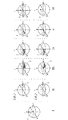
- FIG. 8 is a diagram schematically illustrating electron spin behavior corresponding to the pulse sequence in FIG. 7.
- 6 is a flowchart illustrating a detailed procedure of a quantum operation. It is a flowchart which shows the detailed procedure at the time of sensing a static magnetic field. This is a pulse sequence for sensing a static magnetic field.
- FIG. 12 is a diagram schematically illustrating electron spin behavior corresponding to the pulse sequence in FIG. 11. Is a graph showing the measurement results of the decoherence time T 2 in the first embodiment.
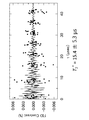
- 11 is a graph showing a measurement result of a decoherence time T 2 * for an electron spin in a dressed state in Example 2.
- 11 is a graph showing a measurement result of a decoherence time T 2 * for an electron spin in a bare state in Example 2.
- 13 is a graph showing the correspondence between the intensity of the magnetic resonance signal and the static magnetic field of the measurement target in Example 3.
- the physical quantity means a quantity whose dimension is determined under a certain system in physics and can be expressed as a multiple of a predetermined physical unit.
- the physical quantity include, for example, a magnetic field, an electric field, a temperature, and a mechanical quantity (mechanical stress, pressure, and the like).
- the magnetic field, electric field, and mechanical quantity include a physical quantity that does not change with time and a physical quantity whose direction repeatedly changes with time. That is, the magnetic field includes a static magnetic field and an AC magnetic field, the electric field includes an electrostatic field and an AC electric field, and the mechanical quantity includes a static mechanical quantity and an AC dynamic quantity.
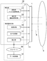
- FIG. 1 is a diagram schematically illustrating a schematic configuration of a measuring device 10 according to an embodiment of the present invention.
- the measurement device 10 includes the sensor element 1, the irradiation unit 2, and the physical quantity measurement unit 3.
- a confocal laser microscope can be used for the configuration of the measuring device 10.
- the sensor element 1 is a diamond crystal having a color center, and uses the NV center as the color center.
- the NV center is a complex (complex defect) of nitrogen (N) substituted for a carbon atom and a vacancy (V) adjacent to the nitrogen.
- the sensor element 1 is attached to the tip of the probe 11 of the measuring device 10.
- the electron spin state of the color center of the sensor element 1 is changed by the interaction 8 with the measurement object 9.
- the interaction 8 is an interaction by an alternating magnetic field.
- the interaction 8 is based on the AC magnetic field, the electron spin state of the color center of the sensor element 1 is in a state according to the intensity of the AC magnetic field generated from the measurement target 9.
- the irradiation unit 2 includes a driving microwave irradiation unit 21 and an operation electromagnetic wave irradiation unit 22.
- the driving microwave irradiator 21 irradiates the sensor element 1 with a driving microwave for generating a dressed state (dressed state) in the electron spin state of the color center. The details of the drest state will be described later.
- the operation electromagnetic wave irradiation unit 22 irradiates the sensor element 1 with an operation electromagnetic wave for operating the electron spin state of the color center.
- the driving microwave is applied to the sensor element 1 in the form of a continuous wave (continuous wave) or in the form of a pulse
- the operating electromagnetic wave is applied to the sensor element 1 in the form of a pulse. 1 is irradiated.
- a known microwave (microwave, ⁇ MW) oscillator can be used for the driving microwave irradiation unit 21 and the operation electromagnetic wave irradiation unit 22.
- the physical quantity measurement unit 3 calculates the physical quantity of the measurement target 9 based on the electron spin state in the dressed state of the color center after the interaction with the measurement target 9. In the present embodiment, the physical quantity measurement unit 3 calculates the intensity of the AC magnetic field generated from the measurement target 9.
- the physical quantity measurement unit 3 includes a quantum circuit unit 31, a light irradiation unit 32, a detection unit 33, and a data processing unit 34.
- the quantum circuit unit 31 performs a quantum operation on phase information between a plurality of energy levels for the electron spin state in the dressed state after the interaction with the measurement target 9.
- the quantum circuit unit 31 is realized by a method based on magnetic resonance using a quantum gate using, for example, an electromagnetic wave pulse. Details of the quantum operation will be described later.
- the quantum circuit unit 31 can be configured using a known microwave oscillator (pulse generator) and a microwave switch.
- the microwave oscillator used for the configuration of the quantum circuit unit 31 and the microwave oscillator used for the configuration of the irradiation unit 2 may be separate devices or may be configured integrally.
- the light irradiation unit 32 irradiates the sensor element 1 with light for reading out the phase information after the quantum operation.
- the light irradiator 32 irradiates the sensor element 1 with light for initializing the electron spin state of the color center.
- various known laser generators can be used for the light irradiation unit 32.
- the light irradiation unit 32 can include an acousto-optic modulator (Acoustic Optical Modulator: AOM).
- AOM Acoustic Optical Modulator
- the acousto-optic modulator can pulse the input laser light and output it.
- the detection unit 33 detects a change occurring in the sensor element 1.
- the detection unit 33 detects the light emitted from the sensor element 1 and uses the known optically detected magnetic resonance (Optically Detected Magnetic Resonance: ⁇ ODMR) method to change the signal of the magnetic resonance to change in emission intensity.
- a known photodiode can be used as the detection unit 33.
- an avalanche photodiode can be used as the photodiode.
- the irradiation unit 2 irradiates the electromagnetic wave for operation in a pulsed form. Therefore, in the present embodiment, specifically, detection is performed by the Pulsed Optically Detected Magnetic Resonance (pODMR) method.
- pODMR Pulsed Optically Detected Magnetic Resonance
- the data processing unit 34 is connected to the detection unit 33, reads out the phase information after the quantum operation from the change detected by the detection unit 33, and calculates the physical quantity of the measurement target 9 based on the read out phase information. In the present embodiment, the data processing unit 34 calculates the strength of the AC magnetic field generated from the measurement target 9.
- a known general-purpose computer or various information terminal devices such as a smartphone can be used. These information terminal devices include a processor that processes data.
- the data processing unit 34 may be configured by an electronic circuit instead of the processor.
- the data processing unit 34 may be configured integrally with the measurement device 10, or may be provided outside the measurement device 10 and connected to the measurement device 10 via the network 99 as illustrated. You may.
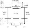
- FIG. 2 is a diagram schematically showing a change in the energy level of electron spin at the NV center during a series of measurement procedures.
- represents m s, with m I>.
- ms is the electron spin of the NV center, and
- m I is the nuclear spin of nitrogen ( 14 N).
- ⁇ 2 > is generated in the electron spin state at the center of NV, and the phases of the generated plurality of dressed states
- the decoherence time of the electron spin increases.
- the reason why the decoherence time is increased is that the microwave mode is strong against external noise. In other words, the coupling between the microwave mode and the NV center makes the noise including the NV center strong, so that it is difficult to attenuate, and as a result, the decoherence time increases.
- the minimum strength B min of the detectable magnetic field decreases due to the addition by the quantum operation and the increase in the decoherence time, and the measurement sensitivity of the magnetic field improves.
- the measurement sensitivity is improved by using such a sensor element 1 in which the electron spin state of the color center is a dressed state.
- a microwave-dressed state is a new quantum state generated by coupling a target system and a mode of a microwave applied to the target.
- the drest state is a state in which electron spins are dressed in microwave clothing.
- the generation of the microwave dressed state in the present invention is based on the Autler-Townes ⁇ splitting ⁇ (ATS) method.
- the intensity and frequency of the driving microwave applied to the sensor element 1 can be appropriately determined based on the ATS method.
- FIG. 2A shows a state before the generation of the dressed state.
- the ground state of the NV center is a spin triplet state, and the spin triplet state of the ground state is excited by light absorption. In the steady state at room temperature, all levels are equally distributed in the ground state. In this state, when the NV center is optically excited using laser light, the distribution probability of each level is unevenly distributed, and the ground state of the NV center becomes a polarized state.
- the ground state of the NV center after laser beam irradiation is expressed as
- FIG. 3 is a diagram schematically showing the energy levels of electron spins at the NV center before and after the generation of the dressed state.
- (A) shows the state before the generation of the dressed state, and (b) shows the state after the generation of the dressed state.
- FIG. 2B shows a state where the magnetic field sensing is performed after the generation of the dressed state.
- n + 1> are driving microwave modes, and n is a positive integer including 0 (0, 1, 2,).
- N + 1> is equal to the driving microwave intensity ⁇ drive . That is, it is possible to simultaneously operate between two levels with a microwave having a frequency equal to ⁇ drive . This means that two levels in the dressed state are measured simultaneously by one magnetic field sensing. The detailed procedure of the magnetic field sensing will be described later.
- FIG. 2C shows a state in which phase information after the quantum operation is read.
- ⁇ 2 > is detected by quantum operation.
- a quantum circuit unit to be described later is used for the addition by the quantum operation.
- ⁇ 1,0> is used as an auxiliary state (ancilla state) used as an auxiliary operation during the quantum operation.
- -1, -1> of the NV center is determined by an optical detection magnetic resonance (ODMR) method.
- ODMR optical detection magnetic resonance
- the signal is detected as a change in emission intensity.
- the change in light emission intensity includes phase information after the quantum operation.
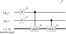
- FIG. 4 is a diagram schematically showing a quantum circuit unit that performs a quantum operation on a dressed state.
- the quantum circuit unit 31 includes a first Hadamard acting unit 51, a second Hadamard acting unit 52, a first unitary acting unit 53, and a second unitary acting unit 54.
- the quantum circuit unit 31 uses the state
- the output after the action by the first unitary action section 53 and the output after the action by the second unitary action section 54 are added to the auxiliary state.
- the first Hadamard acting section 51 acts on the dressed state 1
- the first unitary action section 53 acts on the output of the first Hadamard action section 51 and adds the output to the auxiliary state
- the second Hadamard acting section 52 acts on the dressed state 2
- the second unitary action section 54 acts on the output of the second Hadamard action section 52 and adds the output to the auxiliary state
- the first Hadamard gate action section 51 and the second Hadamard gate action section 52 function as a Hadamard gate
- the unit 54 functions as a unitary operator (unitary gate).
- the phase information added to the assist state is detected as a change in light emission intensity by an optical detection magnetic resonance (ODMR) method.
- the detected phase information is in a state according to the physical quantity to be measured. Therefore, by appropriately performing data processing on the detected phase information of the electron spin state after the interaction, the physical quantity of the measurement target can be calculated.
- the physical quantity to be measured can be calculated based on the Hamiltonian of the electron spin.
- the Hamiltonian Hgs of the electron spin is represented by the following equation.
- mu B is the Bohr magneton
- g e is the g factor of the electron
- h is Planck's constant
- Vector S is an electron spin.
- Vector B is the applied magnetic field.
- D gs is the zero field splitting constant.
- S x , S y , and S z are the x, y, and z direction components of the electron spin S, respectively.
- d gs ⁇ is the electric dipole moment.
- Each E x, E y is the electric field of x, a y-direction component.
- First term Is a term based on the Zeeman effect, which means that electron spin functions as a magnetic field sensor.
- the second and third terms are due to dipole interactions (ie, spin-spin interactions).
- Second term Means that the electron spin functions as a temperature sensor and a mechanical quantity (pressure) sensor.
- Third term Means that the electron spin functions as an electric field sensor.
- the strength of the magnetic field can be calculated based on the first term.
- the intensity of the temperature and the dynamic quantity can be calculated based on the second term.
- the electric field strength can be calculated based on the third term.
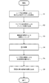
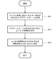
- FIG. 5 is a flowchart showing the procedure of the measurement method according to one embodiment of the present invention.
- step S1 the sensor element 1 is irradiated with laser light to initialize the electron spin at the color center (NV center) of the sensor element 1. Thereafter, the initialized electron spin at the center of the NV interacts with the AC magnetic field of the object 9 to be measured. When the interaction is performed for a sufficient time, the electron spin state at the NV center becomes a state corresponding to the strength of the alternating magnetic field.
- step S2 a dressing state is generated in the electron spin state around the NV by irradiating the sensor element 1 with a driving microwave. As a result, the electron spin state of the NV center of the sensor element 1 becomes a dressed state.
- step S3 magnetic field sensing is performed by irradiating the sensor element 1 with electromagnetic waves for spin operation.
- the sensing of the alternating magnetic field is performed by the procedure shown in steps S31A to S33A of FIG.
- FIG. 6 is a flowchart showing a detailed procedure for sensing an alternating magnetic field.
- FIG. 7 shows a pulse sequence when an alternating magnetic field is sensed.
- FIG. 8 is a diagram schematically showing the behavior of the electron spin corresponding to the pulse sequence of FIG. In FIG. 8, the upper side shows electron spins in the dressed state 1
- State I corresponds to the state of step S1, and represents a state in which electron spin is initialized by irradiation with laser light.
- the electron spins 7 are aligned in a direction along the z axis which is a quantization axis.
- State II corresponds to the state of step S2, and represents a state in which two dressed states have been generated.
- step S31A an operation of tilting the electron spins along the quantization axis to a plane perpendicular to the quantization axis is performed by irradiating a ⁇ / 2 pulse.
- the electron spin 7 is tilted to the xy plane.
- the phase of the electron spin 7 tilted on the xy plane is relaxed during a predetermined time ⁇ by the interaction with the alternating magnetic field and the static magnetic field.
- the time ⁇ is a time corresponding to a half wavelength of the AC magnetic field to be measured.
- step S32A an operation of irradiating a ⁇ pulse to invert the electron spin whose phase has been relaxed by the interaction with the measurement target in a plane.
- the position of the tip of the electron spin 7 is rotated on the xy plane.
- the static magnetic field component is canceled by the reconvergence of the electron spin 7, but the AC magnetic field component is not canceled because the intensity is inverted from that in the state III.
- step S33A an operation of projecting the phase-relaxed electron spin onto the quantization axis by irradiating a ⁇ / 2 pulse is performed.
- the electron spins 7 located in the xy plane are projected on the z axis, which is the quantization axis, and aligned in the direction along the z axis.
- State VII corresponds to the state of step S4 described later
- state VIII corresponds to the state of step S5 described later.
- ⁇ ⁇ Refer to FIG. 5 and FIG. 4 again.
- a quantum operation is performed on phase information between a plurality of energy levels for the electron spin state in the dressed state.
- FIG. 9 is a flowchart showing a detailed procedure of the quantum operation.
- step S41 a Hadamard gate is applied to each of a plurality of energy levels.
- the first Hadamard action part 51 is applied to the drest state 1
- step S42 a unitary operator is applied to each of the outputs of the plurality of Hadamard gates.
- the first unitary action section 53 is applied to the output of the first Hadamard action section 51
- the second unitary action section 54 is applied to the output of the second Hadamard action section 52.
- step S43 each output of the plurality of unitary operators is added to the quantum auxiliary state.
- the phase information output from the two unitary action units 53 and 54 is added to the auxiliary state
- step S5 the phase information after the quantum operation is read out by irradiating the sensor element 1 with laser light and detecting a change occurring in the sensor element 1.
- step S5 by detecting the light emitted from the sensor element 1, the phase information after the quantum operation of the electron spin state after the interaction is read.
- ⁇ 1, 0> is moved to the state
- -1, -1> after the movement is detected by the detection unit 33 as a change in the emission intensity by the optical detection magnetic resonance (ODMR) method.
- ODMR optical detection magnetic resonance
- step S5 the signal strength can be integrated to improve the S / N.
- step S6 the intensity of the magnetic field to be measured is calculated.
- the phase information of the electron spin state after the interaction detected by the detection unit 33 is in a state corresponding to the AC magnetic field of the measurement target 9. Therefore, by appropriately performing data processing on the detected phase information of the electron spin state after the interaction, the intensity of the AC magnetic field can be calculated.
- the strength of the AC magnetic field of the measurement target 9 can be calculated by calculating the probability that the electron spin state after the interaction becomes the ground state.
- the calculation of the intensity is performed based on the term based on the Zeeman effect of the Hamiltonian H gs of the electron spin.
- the minimum intensity B min of the AC magnetic field that can be detected can be reduced, and the measurement sensitivity of the AC magnetic field can be improved in the measurement using the color center for the sensor.
- the measuring device 10 can operate at room temperature (about 300 K) without using a cooling mechanism.
- a superconducting quantum interferometer which is known as an example of an advanced high-sensitivity magnetic field sensor, requires a cooling mechanism such as liquid nitrogen to maintain a superconducting state.
- the measuring device 10 according to the embodiment of the present invention does not need to include a cooling mechanism, the device can be reduced in size or mounted on another device (for example, mounted on transportation equipment such as a car). Is advantageous in comparison with other advanced magnetic field sensors.
- the detailed procedure of the magnetic field sensing in step S3 is different from the procedure in the first embodiment.
- Other procedures are the same as the procedures in the first embodiment.
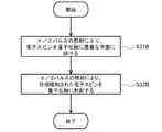
- FIG. 10 is a flowchart showing a detailed procedure for sensing a static magnetic field.
- FIG. 11 shows a pulse sequence for sensing a static magnetic field.
- FIG. 12 is a diagram schematically showing the behavior of electron spins corresponding to the pulse sequence of FIG. In FIG. 12, the electron spin in the dressed state 1
- State I corresponds to the state of step S1 shown in the flowchart of FIG. 5, and represents a state in which the electron spin is initialized by the irradiation of the laser beam.
- the electron spins 7 are aligned in a direction along the z axis which is a quantization axis.
- State II corresponds to the state of step S2 shown in the flowchart of FIG. 5, and represents a state in which two dressed states have been generated.
- step S31B an operation of tilting the electron spins along the quantization axis to a plane perpendicular to the quantization axis is performed by irradiating a ⁇ / 2 pulse.
- the electron spin 7 is tilted to the xy plane.
- the phase of the electron spin 7 tilted on the xy plane is relaxed during a predetermined time ⁇ by interaction with the static magnetic field.
- step S32B an operation of projecting the electron spin whose phase has been relaxed by irradiating a ⁇ / 2 pulse onto the quantization axis is performed.
- the electron spins 7 located in the xy plane are projected on the z axis, which is the quantization axis, and aligned in the direction along the z axis.
- state V corresponds to the state of step S4
- state VI corresponds to the state of step S5.
- the measurement sensitivity of the static magnetic field can be improved.
- the number of dressed states to be generated is not limited to two, and a plurality of dressed states can be generated.
- the quantum circuit section 31 includes three Hadamard action sections and three unitary action sections and has three dressed states. It is preferable to add the states
- the physical quantity of the measurement target is a magnetic field (AC magnetic field or static magnetic field), but is not limited to a magnetic field, and an electric field, temperature, and a mechanical quantity (mechanical stress, pressure, etc.) are used as the physical quantity of the measurement target. be able to.
- These physical quantities are physical quantities related to the interaction with the electron spin, and can be calculated based on the Hamiltonian of the electron spin.
- the NV center is used as the color center of the diamond of the sensor element 1, but the color center used is not limited to the NV center. Instead of the NV center, a silicon-vacancy center or a germanium-vacancy center may be used as the diamond color center of the sensor element 1. Further, the color center is not limited to the color center of the diamond crystal, and any color center of various crystals can be used for the sensor element 1 as long as a dressed state can be generated in the electron spin state of the color center.
- a magnetic resonance signal related to the electron spin state after the interaction is detected as a change in emission intensity by an optical detection magnetic resonance (ODMR) method.
- the magnetic resonance signal can be measured by a known method of electrically detected magnetic resonance (Electrically Detected Magnetic Resonance: EDMR).
- EDMR Electrode Detected Magnetic Resonance
- a photocurrent depending on the spin state is generated by photoexcitation of the sensor element 1 such as the color center of diamond. This photocurrent is generated due to the difference in the lifetime of the excited state depending on the spin state.
- the detecting unit 33 detects a magnetic resonance signal as a change in electric resistivity (or a change in photocurrent due to light irradiation) by detecting the electric resistance of the sensor element 1 (or the photocurrent generated in the sensor element 1). . That is, the detection unit 33 functions as an electrical detection unit.
- the detection unit 33 for example, a known ammeter can be used.
- the DC magnetic field only needs to be applied to the sensor element 1 at least in a section corresponding to the state III.
- Example 1 based on the measurement method of the first embodiment, by using a pulse sequence for measuring an alternating magnetic field, NV - was measured intensity of the magnetic resonance signals for the electron spin in the dressed state of the. Further, the signal intensity obtained by the measurement, to determine the decoherence time T 2 of the electron spin in the dressed state.
- Figure 13 is a graph showing the measurement results of the decoherence time T 2 in the first embodiment.
- the vertical axis of the graph corresponds to the intensity (echo intensity) of the magnetic resonance signal.
- NV - bare state is in (i.e., not in dressed state) shows the measurement results electron spin decoherence time T 2.
- the measured values of the intensity of the magnetic resonance signal for the electron spin in the dressed state are indicated by square symbols, and the fitting lines of these measured values are indicated by reference numeral 61.
- measured values of the intensity of the magnetic resonance signal from the electron spin in the bare state are indicated by circle symbols, and fitting lines of these measured values are indicated by reference numeral 62.
- decoherence time T 2 of the electron spin in the dressed state is about 1.5 ms
- the decoherence time T 2 of the electron spin in a bare state was about 4.2Myuesu.
- NV - by generating the dressed state of the electron spin decoherence time T 2 are increased to 100-fold higher (approximately 350-fold).
- Example 2 based on the measurement method according to the second embodiment, by using a pulse sequence for measuring the static magnetic field, NV - it was measured intensity of the magnetic resonance signals for the electron spin in the dressed state of the.
- the decoherence time in this case is referred to as T 2 * with respect to the decoherence time T 2 obtained by the echo method. From the signal strength obtained by the measurement, the decoherence time T 2 * of the electron spin in the dressed state was obtained.
- the output of the laser light used for the measurement was about 100 ⁇ W, the pulse width of the laser light was about 10 ⁇ s, and the pulse width of the ⁇ pulse was about 42 ns.
- FIG. 14 is a graph showing the measurement result of the decoherence time T 2 * for the electron spin in the dressed state in Example 2.
- the measured values of the intensity of the magnetic resonance signal are indicated by square symbols, and the fitting lines of these measured values are indicated by solid lines.
- the decoherence time T 2 * of the electron spin in the dressed state was 15.4 ⁇ 5.3 ⁇ s.
- the intensity of a magnetic resonance signal was measured for electron spins in a bear state of NV ⁇ .
- the decoherence time T 2 * of the electron spin in the bare state was obtained.
- the output of the laser light used for the measurement was about 100 ⁇ W
- the pulse width of the laser light was about 10 ⁇ s
- the pulse width of the ⁇ pulse was about 44 ns.
- FIG. 15 is a graph showing the measurement results of the decoherence time T 2 * for the electron spin in the bare state in Example 2.
- the measured values of the intensity of the magnetic resonance signal are indicated by square symbols, and the fitting lines of these measured values are indicated by solid lines.
- the decoherence time T 2 * of the electron spin in the bare state was 0.95 ⁇ 0.27 ⁇ s.
- Example 3 in the case of measuring the static magnetic field, the detection sensitivity was compared between the case where the dressed state was generated in the electron spin and the case where the dressed state was not generated (in the bare state) for the electron spin.
- the measurement of the intensity of the magnetic resonance signal was performed under the same conditions as in Example 2.
- the time ⁇ between ⁇ / 2 pulses in the pulse sequence was 25 ⁇ s.
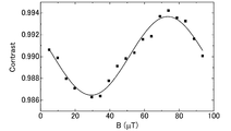
- FIG. 16 is a graph illustrating the correspondence between the intensity of the magnetic resonance signal and the static magnetic field of the measurement target according to the third embodiment.
- the graph shown in FIG. 16 was obtained by changing the magnitude of the static magnetic field of the measurement target.
- the measured values of the intensity of the magnetic resonance signal are indicated by square symbols, and the fitting lines of these measured values are indicated by solid lines.
- the detection sensitivity was calculated based on the slope of the fitting line of the graph shown in FIG. 16 and the standard deviation ⁇ of the measured value of the intensity of the magnetic resonance signal shown on the vertical axis of the graph.
- a graph similar to that shown in FIG. 16 was created even when a dressed state was not generated in the electron spin, and the detection sensitivity was calculated from the created graph. Table 1 shows the calculation results of the detection sensitivity.
Landscapes
- Physics & Mathematics (AREA)
- General Physics & Mathematics (AREA)
- Engineering & Computer Science (AREA)
- Theoretical Computer Science (AREA)
- Condensed Matter Physics & Semiconductors (AREA)
- General Engineering & Computer Science (AREA)
- Evolutionary Computation (AREA)
- Data Mining & Analysis (AREA)
- Mathematical Analysis (AREA)
- Mathematical Optimization (AREA)
- Pure & Applied Mathematics (AREA)
- Computing Systems (AREA)
- Computational Mathematics (AREA)
- Mathematical Physics (AREA)
- Software Systems (AREA)
- Artificial Intelligence (AREA)
- High Energy & Nuclear Physics (AREA)
- Health & Medical Sciences (AREA)
- Life Sciences & Earth Sciences (AREA)
- Chemical & Material Sciences (AREA)
- Analytical Chemistry (AREA)
- Biochemistry (AREA)
- General Health & Medical Sciences (AREA)
- Immunology (AREA)
- Pathology (AREA)
- Measuring Magnetic Variables (AREA)
Abstract
色中心をセンサに用いる測定において、測定感度を向上させるために、センサ素子(1)は、ダイヤモンドの結晶構造に色中心を有し、かつ色中心の電子スピン状態がドレスト状態である。
Description
本発明は、色中心をセンサに用いるセンサ素子、測定装置および測定方法に関する。
ダイヤモンドの結晶構造において、窒素-空孔中心と呼ばれる複合欠陥が見られることがある。この窒素-空孔中心は、結晶格子の炭素原子の位置に置き換わる形で入った窒素原子と、その窒素原子の隣接位置に存在する(炭素原子が抜けている)空孔との対からなるもので、NV中心(Nitrogen Vacancy center)とも呼ばれている。ダイヤモンドの結晶構造には、NV中心以外にも、珪素-空孔中心(Silicon Vacancy center)と呼ばれる複合欠陥や、ゲルマニウム-空孔中心(Germanium Vacancy center)と呼ばれる複合欠陥が見られることがあり、NV中心を含むこれら複合欠陥は、色中心と呼ばれている。
NV中心は、空孔に電子が捕獲された状態(負電荷状態、以下「NV-」と呼ぶ)においては、電子スピンと呼ばれる磁気的な性質を示す。このNV-は、電子が捕獲されていない状態(中性状態、以下「NV0」と呼ぶ)に比べて、長い横緩和時間(デコヒーレンス時間、以下「T2」と呼ぶ)を示す。つまり、NV-の電子スピン状態は、外部磁場の縦方向(以下、「量子化軸」と呼ぶ)に揃えた電子スピンの磁化を横方向に傾けた後、個々のスピンの歳差運動が原因となり個々の向きがずれていって、全体としての横磁化が消失するまでの時間が長い。また、NV-は、室温(約300K)下であっても長いT2値を示す。
NV-の電子スピン状態は外部の磁場に反応して変化し、この電子スピン状態の測定も室温下で可能であるため、NV中心を含むダイヤモンドは、磁場センサ素子の材料として利用できる。
さらに、NV-の電子スピン状態は、電磁波照射などの方法により、外部から人為的に操作する(特定の電子スピン状態に置く)こともできる。この操作も室温下で可能であるため、T2が長いことと合わせて、NV中心は、量子状態の書き込みおよび読み出しが安定して行える量子ビットとして利用可能なことが期待され、NV中心等の色中心を含むダイヤモンドは、量子情報素子や電子回路素子の材料としての利用が期待されている。
例えば特許文献1には、色中心を含むダイヤモンドを用いたセンサが開示されている。
このような、ダイヤモンド中の色中心をセンサに用いる磁場等の測定において、測定感度をさらに向上することが求められている。
一例として、磁場を測定する場合について説明する。ダイヤモンド中の色中心を用いたセンサによる磁場測定の検出感度は、次の式で表される。

ここで、Bminは、検出可能な磁場の最小強度であり、Nは量子ビット数である。デコヒーレンス時間T2が増大すると検出可能な磁場の最小強度Bminも減少することから、測定感度をさらに向上させるために、デコヒーレンス時間をさらに増大させることが求められている。
本発明は、色中心をセンサに用いる測定において、測定感度を向上させることを目的とする。
上記目的を達成するための本発明は、例えば以下に示す態様を含む。
(項1)
ダイヤモンドの結晶構造に色中心を有し、かつ色中心の電子スピン状態がドレスト状態であるセンサ素子。
(項2)
前記色中心は、1つの炭素原子を置換した窒素(N)と前記窒素に隣接する空孔(V)とを含んでいるダイモンドの複合体である、項1に記載のセンサ素子。
(項3)
測定対象との相互作用により変化する色中心の電子スピン状態にドレスト状態を生成するための駆動用のマイクロ波と、前記電子スピン状態を操作するための操作用の電磁波とを、前記色中心を有するセンサ素子に照射する照射部と、
前記測定対象との相互作用後の、前記ドレスト状態にある前記電子スピン状態に基づいて、前記測定対象の物理量を算出する物理量測定部と、
を備える、測定装置。
(項4)
前記物理量測定部は、
前記測定対象との相互作用後の、前記ドレスト状態にある前記電子スピン状態について、複数のエネルギー準位間の位相の情報を量子演算する量子回路部と、
前記量子演算後の前記位相の情報を読み出すための光を、前記センサ素子に照射する光照射部と、
前記光の照射によって前記センサ素子に生じる変化を検出する検出部と、
前記検出された変化から前記量子演算後の前記位相の情報を読み出し、読み出した前記位相の情報に基づいて前記物理量を算出するデータ処理部と、
を備える、項3に記載の測定装置。
(項5)
前記量子回路部は、
前記複数のエネルギー準位のそれぞれに作用する複数のアダマール作用部と、
複数の前記アダマール作用部の出力のそれぞれに作用し、量子的な補助状態に出力を加算する複数のユニタリ作用部と、
を備える、項4に記載の測定装置。
(項6)
前記色中心は、炭素原子を置換した窒素(N)と前記窒素に隣接する空孔(V)との複合体である、項3から5のいずれか1項に記載の測定装置。
(項7)
前記物理量測定部は、電子スピンとの相互作用に関連する前記物理量として、磁場、電場、温度および力学量のうち、少なくとも一つを算出する、項3から6のいずれか1項に記載の測定装置。
(項8)
色中心を有するセンサ素子に、測定対象との相互作用により変化する前記色中心の電子スピン状態にドレスト状態を生成するための駆動用のマイクロ波を照射するステップと、
前記電子スピン状態を操作するための操作用の電磁波を、前記センサ素子に照射するステップと、
前記測定対象との相互作用後の、前記ドレスト状態にある前記電子スピン状態に基づいて、前記測定対象の物理量を算出するステップと、
を含む、測定方法。
(項9)
前記物理量を算出するステップは、
前記ドレスト状態にある前記電子スピン状態について、複数のエネルギー準位間の位相の情報を量子演算するステップと、
前記量子演算後の前記位相の情報を読み出すための光を、前記センサ素子に照射するステップと、
前記光の照射によって前記センサ素子に生じる変化を検出するステップと、
前記検出された変化から前記量子演算後の前記位相の情報を読み出し、読み出した前記位相の情報に基づいて前記物理量を算出するステップと、
を含む、項8に記載の測定方法。
(項10)
前記量子演算を行うステップは、
前記複数のエネルギー準位のそれぞれにアダマールゲートを作用させるステップと、
複数の前記アダマールゲートの出力のそれぞれにユニタリ作用素を作用させ、複数の前記ユニタリ作用素の出力のそれぞれを、量子的な補助状態に加算するステップと、
を含む、項9に記載の測定方法。
(項11)
前記操作用の電磁波を照射するステップは、
π/2パルスを照射することにより、量子化軸に沿った電子スピンを、前記量子化軸に垂直な平面に傾ける操作を行うステップと、
πパルスを照射することにより、前記測定対象との相互作用により位相緩和された前記電子スピンを、前記平面内において反転させる操作を行うステップと、
π/2パルスを照射することにより、位相緩和された前記電子スピンを、前記量子化軸に射影する操作を行うステップと、
を含む、項8から10のいずれか1項に記載の測定方法。
(項12)
前記操作用の電磁波を照射するステップは、
π/2パルスを照射することにより、量子化軸に沿った電子スピンを、前記量子化軸に垂直な平面に傾ける操作を行うステップと、
π/2パルスを照射することにより、前記測定対象との相互作用により位相緩和された前記電子スピンを、前記量子化軸に射影する操作を行うステップと、
を含む、項8から10のいずれか1項に記載の測定方法。
本発明によると、色中心をセンサに用いる測定において、測定感度を向上させることができる。
以下、本発明の実施形態を、添付の図面を参照して詳細に説明する。なお、以下の説明および図面において、同じ符号は同じまたは類似の構成要素を示すこととし、よって、同じまたは類似の構成要素に関する重複した説明を省略する。
なお、本明細書において、物理量(physical quantity)とは、物理学における一定の体系の下で次元が確定し、定められた物理単位の倍数として表すことができる量を意味する。物理量の一例としては、例えば、磁場、電場、温度および力学量(力学的なストレス、圧力等)が挙げられる。磁場、電場および力学量は、時間と共に変化しない物理量と、時間と共に方向が変化を繰り返す物理量とを含む。すなわち、磁場は、静磁場および交流磁場を含み、電場は、静電場および交流電場を含み、力学量は、静的な力学量および交流力学量を含む。
[第1の実施形態]
本発明の第1の実施形態では、測定対象の物理量の一例として、測定対象から発生している交流磁場(alternating magnetic field)の強度を測定する場合について説明する。
本発明の第1の実施形態では、測定対象の物理量の一例として、測定対象から発生している交流磁場(alternating magnetic field)の強度を測定する場合について説明する。
[装置構成]
図1は、本発明の一実施形態に係る測定装置10の概略的な構成を模式的に示す図である。
図1は、本発明の一実施形態に係る測定装置10の概略的な構成を模式的に示す図である。
測定装置10は、センサ素子1と、照射部2と、物理量測定部3と、を備える。一例として、本実施形態では、共焦点レーザ顕微鏡を測定装置10の構成に用いることができる。
本実施形態では、センサ素子1は、色中心を有しているダイヤモンドの結晶であり、色中心としてNV中心を用いる。NV中心は、炭素原子を置換した窒素(N)と、窒素に隣接する空孔(V)との複合体(複合欠陥)である。センサ素子1は、本実施形態では、測定装置10のプローブ11先端に取り付けられている。
センサ素子1が有する色中心の電子スピン状態は、測定対象9との相互作用8により変化を受ける。本実施形態では、相互作用8は交流磁場による相互作用である。相互作用8が交流磁場による場合には、センサ素子1の色中心の電子スピン状態は、測定対象9から発生している交流磁場の強度に応じた状態となる。
照射部2は、駆動用マイクロ波照射部21と、操作用電磁波照射部22とを備える。駆動用マイクロ波照射部21は、色中心の電子スピン状態にドレスト状態(dressed states)を生成するための駆動用のマイクロ波を、センサ素子1に照射する。ドレスト状態の詳細については後述する。操作用電磁波照射部22は、色中心の電子スピン状態を操作するための操作用の電磁波を、センサ素子1に照射する。本実施形態では、駆動用のマイクロ波は、連続波(continuous wave)の形式で、もしくはパルス化された形式でセンサ素子1に照射され、操作用の電磁波は、パルス化された形式でセンサ素子1に照射される。駆動用マイクロ波照射部21および操作用電磁波照射部22には、公知のマイクロ波(microwave, MW)発振器を用いることができる。
物理量測定部3は、測定対象9との相互作用後の、色中心のドレスト状態にある電子スピン状態に基づいて、測定対象9の物理量を算出する。本実施形態では、物理量測定部3は、測定対象9から発生している交流磁場の強度を算出する。物理量測定部3は、量子回路部31と、光照射部32と、検出部33と、データ処理部34とを備える。
量子回路部31は、測定対象9との相互作用後の、ドレスト状態にある電子スピン状態について、複数のエネルギー準位間の位相情報を量子演算する。一例として、量子回路部31は、例えば電磁波パルスによる量子ゲートを用いた磁気共鳴による手法により実現される。量子演算の詳細については後述する。量子回路部31は、公知のマイクロ波発振器(パルスジェネレータ)とマイクロ波スイッチとを用いて構成することができる。量子回路部31の構成に用いるマイクロ波発振器と照射部2の構成に用いるマイクロ波発振器とは、それぞれ別個の機器であってもよいし、一体化して構成されてもよい。
光照射部32は、量子演算後の位相情報を読み出すための光を、センサ素子1に照射する。また、光照射部32は、色中心の電子スピン状態を初期化するための光をセンサ素子1に照射する。光照射部32には、例えば種々の公知のレーザ発生装置を用いることができる。任意の構成として、光照射部32は、音響光学変調素子(Acoustic Optical Modulator: AOM)を備えることができる。音響光学変調素子は、入力されるレーザ光をパルス化して出力することができる。
検出部33は、センサ素子1に生じる変化を検出する。本実施形態では、検出部33は、センサ素子1から放出される光を検出することにより、公知の光検出磁気共鳴(Optically Detected Magnetic Resonance: ODMR)法により、磁気共鳴の信号を発光強度の変化として検出する。この場合、検出部33には、例えば公知のフォトダイオードを用いることができる。フォトダイオードには、例えばアバランシェフォトダイオードを用いることができる。
なお、本実施形態では、照射部2において操作用の電磁波をパルス化した形式で照射している。よって、本実施形態では、具体的にはPulsed Optically Detected Magnetic Resonance(pODMR)法による検出を行う。
データ処理部34は、検出部33と接続され、検出部33にて検出された変化から量子演算後の位相情報を読み出し、読み出した位相情報に基づいて測定対象9の物理量を算出する。本実施形態では、データ処理部34は、測定対象9から発生している交流磁場の強度を算出する。データ処理部34には、例えば公知の汎用コンピュータや、スマートフォン等の種々の情報端末装置を用いることができる。これら情報端末装置は、データを処理するプロセッサを備えている。データ処理部34は、プロセッサに代えて電子回路で構成されてもよい。
データ処理部34は、測定装置10と一体化されて構成されていてもよいし、または図示するように、測定装置10の外部に設けられて、ネットワーク99を介して測定装置10と接続されていてもよい。
[測定原理]
図2は、一連の測定手順を行う間の、NV中心における電子スピンのエネルギー準位の変化を模式的に示す図である。図中、NV中心の量子状態を|ms,mI>で表す。msはNV中心の電子スピンであり、mIは窒素(14N)の核スピンである。
図2は、一連の測定手順を行う間の、NV中心における電子スピンのエネルギー準位の変化を模式的に示す図である。図中、NV中心の量子状態を|ms,mI>で表す。msはNV中心の電子スピンであり、mIは窒素(14N)の核スピンである。
本発明では、NV中心における電子スピン状態にドレスト状態|φ1>,|φ2>を生成し、生成した複数のドレスト状態|φ1>,|φ2>の位相を、量子演算により足し合わせて検出する。さらにNV中心における電子スピン状態にドレスト状態を生成することにより、電子スピンのデコヒーレンス時間が増大する。デコヒーレンス時間が増大する理由はマイクロ波モードが外部ノイズに強いからである。つまり、マイクロ波モードとNV中心が結合することによって、NV中心も含めてノイズに強くなることから減衰しにくくなり、その結果デコヒーレンス時間が増大する。つまり、量子演算による足し合わせとデコヒーレンス時間の増大により検出可能な磁場の最小強度Bminが減少し、磁場の測定感度が向上する。本発明では、物理量の測定において、色中心の電子スピン状態がドレスト状態であるこのようなセンサ素子1を用いることにより、測定感度を向上させている。
マイクロ波によるドレスト状態とは、対象の系(system)と対象に照射するマイクロ波のモードとが結合することにより生成される新たな量子状態である。ドレスト状態とは、電子スピンがマイクロ波の衣をまとった状態のことである。本発明におけるマイクロ波ドレスト状態の生成は、Autler-Townes splitting (ATS)法に基づいている。センサ素子1に照射する駆動用のマイクロ波の強度および周波数等は、ATS法に基づいて適宜決定することができる。
図2(a)は、ドレスト状態生成前の状態を示している。NV中心の基底状態はスピン三重項状態であり、光の吸収により、基底状態のスピン三重項状態は励起される。室温における定常状態では、基底状態において全ての準位は等しく分布している。この状態において、レーザ光を用いてNV中心を光励起すると、各準位の分布確率が偏在し、NV中心の基底状態は偏極状態となる。レーザ光照射後の、NV中心の基底状態は、|0,0>、|0,1>および|0,-1>と表される。
図3は、ドレスト状態を生成する前および後の、NV中心における電子スピンのエネルギー準位を模式的に示す図である。ドレスト状態生成前の状態を(a)に示し、ドレスト状態生成後の状態を(b)に示す。図2(b)は、ドレスト状態生成後に磁場センシングを行う状態を示している。
NV中心の基底状態|0,-1>と励起状態|-1,-1>との間の共鳴周波数ωdriveで相当する駆動用のマイクロ波をその強度ΩdriveでNV中心に照射すると、NV中心の電子スピン状態には、2つのドレスト状態|φ1>、|φ2>が生成される。具体的には、|-1,-1>および|0,-1>の2つの準位に関してドレスト状態を生成すると、|-1,-1>|n>、|0,-1>|n+1>、|-1,-1>|n-1>、および|0,-1>|n>の4準位が生成される。ここで、|n-1>、|n>、|n+1>は駆動用のマイクロ波のモードであり、nは0を含む正の整数(0,1,2,・・・)である。このとき、|-1,-1>|n-1>と|0,-1>|n>との間の分裂幅、および|-1,-1>|n>と|0,-1>|n+1>との間の分裂幅Ωは、駆動用のマイクロ波の強度Ωdriveと等しい。すなわち、Ωdriveと等しい周波数のマイクロ波によって、2つの準位間を同時に操作することが可能である。これは、1回の磁場センシングにより、ドレスト状態にある2つの準位を同時に測定していることを意味している。磁場センシングの詳細な手順については後述する。
図2(c)は、量子演算後の位相情報を読み出す状態を示している。
磁場センシングを行った後、生成した2つのドレスト状態|φ1>,|φ2>の位相情報を、量子演算により足し合わせて検出する。量子演算による足し合わせには、後述する量子回路部を用いる。量子演算時に演算の補助として用いる補助状態(ancilla state)には、本実施形態では、例えば|-1,0>を用いる。その後、量子演算による足し合わせ後の状態について、光検出磁気共鳴(ODMR)法により、NV中心の基底状態|0,-1>と励起状態|-1,-1>との間の磁気共鳴の信号を、発光強度の変化として検出する。発光強度の変化には、量子演算後の位相情報が含まれている。
図4は、ドレスト状態に対する量子演算を行う量子回路部を模式的に示す図である。
量子回路部31は、第1のアダマール作用部51と、第2のアダマール作用部52と、第1のユニタリ作用部53と、第2のユニタリ作用部54と、を備える。本実施形態では、量子回路部31は、状態|-1,0>を、演算を補助するための補助状態に用いる。補助状態には、第1のユニタリ作用部53による作用後の出力と第2のユニタリ作用部54による作用後の出力とが加算される。
第1のアダマール作用部51は、ドレスト状態1|φ1>に作用する。第1のユニタリ作用部53は、第1のアダマール作用部51の出力に作用して、出力を補助状態|-1,0>に加算する。第2のアダマール作用部52は、ドレスト状態2|φ2>に作用する。第2のユニタリ作用部54は、第2のアダマール作用部52の出力に作用して、出力を補助状態|-1,0>に加算する。例えば量子ゲートにて実装される量子回路において、第1のアダマールゲート作用部51および第2のアダマールゲート作用部52は、アダマールゲートとして機能し、第1のユニタリ作用部53および第2のユニタリ作用部54は、ユニタリ作用素(ユニタリゲート)として機能する。
補助状態に加算した位相情報は、光検出磁気共鳴(ODMR)法により、発光強度の変化として検出する。検出した位相情報は、測定対象の物理量に応じた状態となっている。よって、検出した相互作用後の電子スピン状態の位相情報を、適切にデータ処理することにより、測定対象の物理量を算出することができる。測定対象の物理量は、電子スピンのハミルトニアンに基づいて算出することができる。
電子スピンのハミルトニアンHgsは、以下の式で表される。
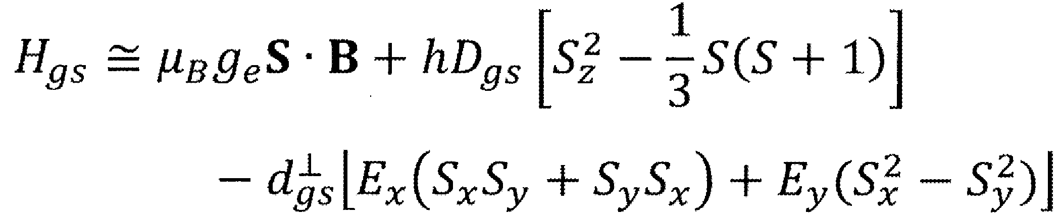
ここで、μBはボーア磁子であり、geは電子のg因子であり、hはプランク定数である。ベクトルSは電子スピンである。ベクトルBは印加磁場である。Dgsは零磁場分裂定数である。Sx,Sy,Szはそれぞれ、電子スピンSのx,y,z方向成分である。dgs
⊥は、電気双極子モーメントである。Ex,Eyはそれぞれ、電場のx,y方向成分である。
1番目の項

は、ゼーマン効果による項であり、電子スピンが磁場センサとして機能することを意味している。
2番目の項および3番目の項は、双極子相互作用(すなわち、スピン間相互作用)による項である。2番目の項

は、電子スピンが温度センサおよび力学量(圧力)センサとして機能することを意味している。3番目の項

は、電子スピンが電場センサとして機能することを意味している。
よって、磁場の強度は、1番目の項に基づいて算出することができる。温度および力学量の強度は、2番目の項に基づいて算出することができる。電場の強度は、3番目の項に基づいて算出することができる。
[測定手順]
図5は、本発明の一実施形態に係る測定方法の手順を示すフローチャートである。
図5は、本発明の一実施形態に係る測定方法の手順を示すフローチャートである。
ステップS1において、センサ素子1にレーザ光を照射することにより、センサ素子1の色中心(NV中心)の電子スピンを初期化する。その後、初期化されたNV中心の電子スピンを、測定対象9の交流磁場と相互作用させる。十分な時間の間、相互作用をさせると、NV中心の電子スピン状態は、交流磁場の強度に応じた状態となる。
ステップS2において、センサ素子1に駆動用のマイクロ波を照射することにより、NV中心の電子スピン状態にドレスト状態を生成する。これにより、センサ素子1のNV中心の電子スピン状態はドレスト状態となる。
ステップS3において、センサ素子1にスピン操作用の電磁波を照射することにより、磁場センシングを行う。本実施形態では、図6のステップS31A~S33Aに示す手順により、交流磁場のセンシングを行う。
<交流磁場のセンシング>
図6は、交流磁場をセンシングする場合の詳細な手順を示すフローチャートである。図7は、交流磁場をセンシングする場合のパルスシーケンスである。図8は、図7のパルスシーケンスに対応する電子スピンの挙動を模式的に示す図である。図8中、上側にはドレスト状態1|φ1>の電子スピンを示し、下側にはドレスト状態2|φ2>の電子スピンを示している。
図6は、交流磁場をセンシングする場合の詳細な手順を示すフローチャートである。図7は、交流磁場をセンシングする場合のパルスシーケンスである。図8は、図7のパルスシーケンスに対応する電子スピンの挙動を模式的に示す図である。図8中、上側にはドレスト状態1|φ1>の電子スピンを示し、下側にはドレスト状態2|φ2>の電子スピンを示している。
状態Iは、ステップS1の状態に対応しており、レーザ光の照射により電子スピンを初期化した状態を表している。電子スピン7は、量子化軸であるz軸に沿った方向に揃っている。状態IIは、ステップS2の状態に対応しており、2つのドレスト状態を生成した状態を表している。
次いで、ステップS31Aにおいて、π/2パルスを照射することにより、量子化軸に沿った電子スピンを、量子化軸に垂直な平面に傾ける操作を行う。状態IIに示すように、電子スピン7はxy平面に倒される。その後、状態IIIに示すように、xy平面に倒された電子スピン7は、所定の時間τの間に、交流磁場および静磁場との相互作用によって位相緩和する。時間τは、測定対象交流磁場の半波長に対応する時間である。
所定の時間τが経過した後、ステップS32Aにおいて、πパルスを照射することにより、測定対象との相互作用により位相緩和された電子スピンを、平面内において反転させる操作を行う。状態IIIから状態IVに示すように、電子スピン7は、xy平面においてその先端の位置が回転している。この際、状態Vに示すように、電子スピン7が再収束することにより、静磁場成分は打ち消されるが、交流磁場成分は、状態IIIのときと強度が反転しているため打ち消されない。
所定の時間τがさらに経過した後、ステップS33Aにおいて、π/2パルスを照射することにより、位相緩和された電子スピンを、量子化軸に射影する操作を行う。状態VIに示すように、xy平面内に位置していた電子スピン7は、量子化軸であるz軸に射影され、z軸に沿った方向に揃えられる。
なお、状態VIIは後述するステップS4の状態に対応しており、状態VIIIは後述するステップS5の状態に対応している。
図5および図4を再び参照する。ステップS4において量子演算を行うことにより、ドレスト状態にある電子スピン状態について、複数のエネルギー準位間の位相情報を量子演算する。
図9は、量子演算の詳細な手順を示すフローチャートである。
ステップS41において、複数のエネルギー準位のそれぞれにアダマールゲートを作用させる。ドレスト状態1|φ1>には第1のアダマール作用部51を作用させ、ドレスト状態2|φ2>には第2のアダマール作用部52を作用させる。

ステップS42において、複数のアダマールゲートの出力のそれぞれにユニタリ作用素を作用させる。第1のアダマール作用部51の出力には第1のユニタリ作用部53を作用させ、第2のアダマール作用部52の出力には第2のユニタリ作用部54を作用させる。
次いで、ステップS43において、複数のユニタリ作用素の出力のそれぞれを、量子的な補助状態に加算する。本実施形態では、2つのユニタリ作用部53,54からの出力である位相情報が補助状態|-1,0>に加算され、その結果、位相情報が2倍される。

図5および図2を再び参照する。ステップS5において、センサ素子1にレーザ光を照射して、センサ素子1に生じる変化を検出することにより、量子演算後の位相情報の読み出しを行う。本実施形態では、センサ素子1から放出される光を検出することにより、相互作用後の電子スピン状態の、量子演算後の位相情報の読み出しを行う。
まず、加算して補助状態|-1,0>に保持されている位相情報を、πパルスを用いることにより状態|-1,-1>に移動させる。次に、移動させた後の、状態|-1,-1>に保持されている位相情報を、光検出磁気共鳴(ODMR)法により、発光強度の変化として検出部33を用いて検出する。
なお、ステップS1からステップS5に示す手順を繰り返し実行することにより、信号強度を積算してS/Nを向上させることができる。
ステップS6において、測定対象の磁場の強度を算出する。検出部33にて検出した相互作用後の電子スピン状態の位相情報は、測定対象9の交流磁場に応じた状態となっている。よって、検出した相互作用後の電子スピン状態の位相情報を適切にデータ処理することにより、交流磁場の強度を算出することができる。例えば、相互作用後の電子スピン状態が基底状態となる確率を求めることにより、測定対象9の交流磁場の強度を算出することができる。強度の算出は、電子スピンのハミルトニアンHgsの、ゼーマン効果による項に基づいて行う。
以上、本発明の第1の実施形態によると、色中心における電子スピン状態にドレスト状態を生成することにより、デコヒーレンス時間T2を増大させることができる。これにより、検出可能な交流磁場の最小強度Bminを減少させることができ、色中心をセンサに用いる測定において、交流磁場の測定感度を向上させることができる。
また、本発明の一実施形態に係る測定装置10は、冷却機構を用いることなく室温(約300K)下にて動作することができる。先進的な高感度の磁場センサの一例として知られている超伝導量子干渉計(superconducting quantum interference device, SQUID)は、超伝導状態を維持するために、例えば液体窒素等による冷却機構を必要としている。これに対し、本発明の一実施形態に係る測定装置10は、冷却機構を備える必要が無いため、装置の小型化や、他の装置への搭載(例えば、自動車等の輸送機器への搭載)が容易である点において、他の先進的な磁場センサと比較して有利である。
[第2の実施形態]
本発明の第2の実施形態では、測定対象の物理量の一例として、測定対象から発生している静磁場(static magnetic field)の強度を測定する場合について説明する。
本発明の第2の実施形態では、測定対象の物理量の一例として、測定対象から発生している静磁場(static magnetic field)の強度を測定する場合について説明する。
第2の実施形態では、ステップS3における磁場センシングの詳細な手順が、第1の実施形態における手順と異なる。これ以外の手順については、第1の実施形態における手順と同様である。
<静磁場のセンシング>
図10は、静磁場をセンシングする場合の詳細な手順を示すフローチャートである。図11は、静磁場をセンシングする場合のパルスシーケンスである。図12は、図11のパルスシーケンスに対応する電子スピンの挙動を模式的に示す図である。図12中、上側にはドレスト状態1|φ1>の電子スピンを示し、下側にはドレスト状態2|φ2>の電子スピンを示している。
図10は、静磁場をセンシングする場合の詳細な手順を示すフローチャートである。図11は、静磁場をセンシングする場合のパルスシーケンスである。図12は、図11のパルスシーケンスに対応する電子スピンの挙動を模式的に示す図である。図12中、上側にはドレスト状態1|φ1>の電子スピンを示し、下側にはドレスト状態2|φ2>の電子スピンを示している。
状態Iは、図5のフローチャートに示すステップS1の状態に対応しており、レーザ光の照射により電子スピンを初期化した状態を表している。電子スピン7は、量子化軸であるz軸に沿った方向に揃っている。状態IIは、図5のフローチャートに示すステップS2の状態に対応しており、2つのドレスト状態を生成した状態を表している。
次いで、ステップS31Bにおいて、π/2パルスを照射することにより、量子化軸に沿った電子スピンを、量子化軸に垂直な平面に傾ける操作を行う。状態IIに示すように、電子スピン7はxy平面に倒される。その後、状態IIIに示すように、xy平面に倒された電子スピン7は、所定の時間τの間に、静磁場との相互作用によって位相緩和する。
所定の時間τがさらに経過した後、ステップS32Bにおいて、π/2パルスを照射することにより、位相緩和された電子スピンを、量子化軸に射影する操作を行う。状態IVに示すように、xy平面内に位置していた電子スピン7は、量子化軸であるz軸に射影され、z軸に沿った方向に揃えられる。
なお、状態VはステップS4の状態に対応しており、状態VIはステップS5の状態に対応している。
以上、本発明の第2の実施形態によると、色中心をセンサに用いる測定において、静磁場の測定感度を向上させることができる。
[その他の形態]
以上、本発明を特定の実施形態によって説明したが、本発明は上記した実施形態に限定されるものではない。
以上、本発明を特定の実施形態によって説明したが、本発明は上記した実施形態に限定されるものではない。
上記した実施形態では、2つのドレスト状態|φ1>, |φ2>を生成しているが、生成するドレスト状態の数は2つに限らず、複数のドレスト状態を生成することができる。例えば3つのドレスト状態|φ1>, |φ2>, |φ3>を生成する場合には、量子回路部31は、3つのアダマール作用部と3つのユニタリ作用部とを備え、3つのドレスト状態|φ1>, |φ2>, |φ3>を足し合わせると良い。
上記した実施形態では、測定対象の物理量は磁場(交流磁場または静磁場)であるが、磁場に限らず、電場、温度および力学量(力学的なストレス、圧力等)を測定対象の物理量とすることができる。これら物理量は、電子スピンとの相互作用に関連する物理量であり、電子スピンのハミルトニアンに基づいて算出することができる。
上記した実施形態では、センサ素子1のダイヤモンドの色中心としてNV中心を用いているが、用いる色中心はNV中心に限定されない。NV中心に代えて、珪素-空孔中心またはゲルマニウム-空孔中心を、センサ素子1のダイヤモンドの色中心に用いてもよい。また、色中心もダイヤモンド結晶の色中心に限定されず、色中心の電子スピン状態にドレスト状態を生成することができる限り、種々の結晶の色中心をセンサ素子1に用いることができる。
上記した実施形態では、相互作用後の電子スピン状態に関する磁気共鳴の信号を、光検出磁気共鳴(ODMR)法により発光強度の変化として検出しているが、磁気共鳴信号を測定する方法はこれに限定されない。例えば、磁気共鳴信号は、公知の電気検出磁気共鳴(Electrically Detected Magnetic Resonance: EDMR)法により測定することができる。電気検出磁気共鳴(EDMR)法では、ダイヤモンドの色中心等のセンサ素子1の光励起により、スピン状態に依存した光電流が生成される。この光電流は、スピン状態に依存した励起状態の寿命の違いにより生成されている。検出部33は、センサ素子1の電気抵抗(またはセンサ素子1に生じる光電流)を検出することにより、磁気共鳴の信号を電気抵抗率の変化(または光照射による光電流の変化)として検出する。すなわち、検出部33は電気的検出部として機能する。検出部33には、例えば公知の電流計を用いることができる。
また、静磁場をセンシングする場合の図11に示すパルスシーケンスにおいて、直流磁場は、少なくとも状態IIIに対応する区間においてセンサ素子1に印加されていればよい。
以下に本発明の実施例を示し、本発明の特徴をより明確にする。
<実施例1>
<実施例1>
実施例1では、第1の実施形態に係る測定方法に基づいて、交流磁場を測定する場合のパルスシーケンスを用いて、NV-のドレスト状態にある電子スピンについて磁気共鳴信号の強度を測定した。また、測定により得られた信号強度から、ドレスト状態にある電子スピンのデコヒーレンス時間T2を求めた。
図13は、実施例1におけるデコヒーレンス時間T2の測定結果を示すグラフである。グラフの縦軸は、磁気共鳴信号の強度(エコー強度)に対応する。グラフには比較のため、NV-のベア状態にある(すなわち、ドレスト状態にない)電子スピンのデコヒーレンス時間T2の測定結果も示す。グラフ中、ドレスト状態にある電子スピンについての磁気共鳴信号の強度の測定値をスクエア記号で示し、これら測定値のフィッティングラインを符号61で示す。同様に、ベア状態にある電子スピンからの磁気共鳴信号の強度の測定値をサークル記号で示し、これら測定値のフィッティングラインを符号62で示す。
測定の結果、ドレスト状態にある電子スピンのデコヒーレンス時間T2は約1.5msであり、ベア状態にある電子スピンのデコヒーレンス時間T2は約4.2μsであった。この実施例1における測定結果によると、NV-の電子スピンにドレスト状態を生成することにより、デコヒーレンス時間T2は100倍以上(約350倍)に増大した。
デコヒーレンス時間T2が増大すると、検出可能な磁場の最小強度Bminは減少し、検出感度は向上する。よって、交流磁場を測定する場合において、NV-の電子スピンにドレスト状態を生成することにより、検出可能な磁場の最小強度Bminが減少し、ダイヤモンド中の色中心を用いたセンサによる磁場測定において、検出感度が向上することが示された。
<実施例2>
<実施例2>
実施例2では、第2の実施形態に係る測定方法に基づいて、静磁場を測定する場合のパルスシーケンスを用いて、NV-のドレスト状態にある電子スピンについて磁気共鳴信号の強度を測定した。エコー法から求められたデコヒーレンス時間T2に対し、この場合のデコヒーレンス時間をT2
*と呼ぶ。測定により得られた信号強度から、ドレスト状態にある電子スピンのデコヒーレンス時間T2
*を求めた。測定に用いたレーザ光の出力は約100μWであり、レーザ光のパルス幅は約10μsであり、πパルスのパルス幅は約42nsであった。
図14は、実施例2におけるドレスト状態にある電子スピンについてのデコヒーレンス時間T2
*の測定結果を示すグラフである。グラフ中、磁気共鳴信号の強度の測定値をスクエア記号で示し、これら測定値のフィッティングラインを実線で示す。測定の結果、ドレスト状態にある電子スピンのデコヒーレンス時間T2
*は、15.4±5.3μsであった。
また、比較のため、NV-のベア状態にある電子スピンについて磁気共鳴信号の強度を測定した。測定により得られた信号強度から、ベア状態にある電子スピンのデコヒーレンス時間T2
*を求めた。測定に用いたレーザ光の出力は約100μWであり、レーザ光のパルス幅は約10μsであり、πパルスのパルス幅は約44nsであった。
図15は、実施例2におけるベア状態にある電子スピンについてのデコヒーレンス時間T2
*の測定結果を示すグラフである。グラフ中、磁気共鳴信号の強度の測定値をスクエア記号で示し、これら測定値のフィッティングラインを実線で示す。測定の結果、ベア状態にある電子スピンのデコヒーレンス時間T2
*は、0.95±0.27μsであった。
図14および図15の各測定結果に示すように、NV-の電子スピンにドレスト状態を生成することにより、デコヒーレンス時間T2
*は約15倍に増大した。よって、静磁場を測定する場合において、NV-の電子スピンにドレスト状態を生成することにより、検出感度が向上することが示された。
<実施例3>
<実施例3>
実施例3では、静磁場を測定する場合について、電子スピンにドレスト状態を生成する場合と電子スピンにドレスト状態を生成しない(ベア状態にある)場合とで検出感度の比較を行った。磁気共鳴信号の強度の測定は、実施例2と同様の条件で行った。パルスシーケンスにおけるπ/2パルス間の時間τは25μsであった。
図16は、実施例3における磁気共鳴信号の強度と測定対象の静磁場との対応関係を示すグラフである。図16に示すグラフは、測定対象の静磁場の大きさを変化させることにより得られた。グラフ中、磁気共鳴信号の強度の測定値をスクエア記号で示し、これら測定値のフィッティングラインを実線で示す。この図16に示すグラフのフィッティングラインの傾きと、グラフの縦軸に示す磁気共鳴信号の強度の測定値の標準偏差σとに基づいて、検出感度を算出した。また、電子スピンにドレスト状態を生成しない場合についても図16と同様のグラフを作成し、作成したグラフから検出感度を算出した。検出感度の算出結果を表1に示す。
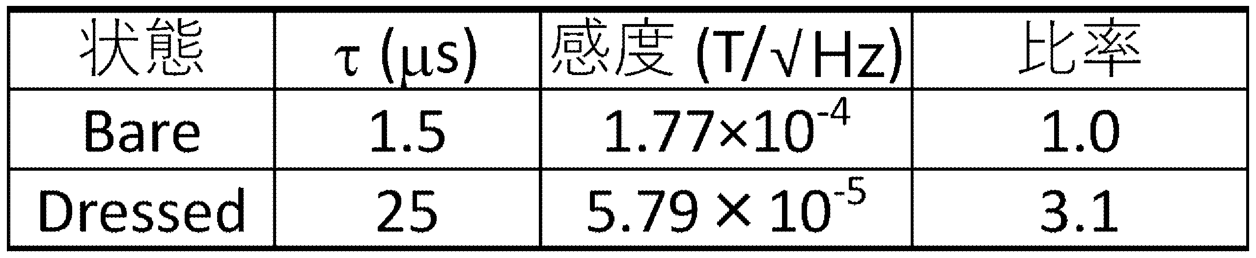
表1の算出結果に示すように、NV-の電子スピンにドレスト状態を生成することにより、検出感度は約3.1倍に増大した。よって、静磁場を測定する場合において、NV-の電子スピンにドレスト状態を生成することにより、検出感度が向上することが確認された。
1 センサ素子
2 照射部
3 物理量測定部
7 電子スピン
8 相互作用
9 測定対象
10 測定装置
11 プローブ
21 駆動用マイクロ波照射部
22 操作用電磁波照射部
31 量子回路部
32 光照射部
33 検出部
34 データ処理部
51,52 アダマール作用部
53,54 ユニタリ作用部
99 ネットワーク
2 照射部
3 物理量測定部
7 電子スピン
8 相互作用
9 測定対象
10 測定装置
11 プローブ
21 駆動用マイクロ波照射部
22 操作用電磁波照射部
31 量子回路部
32 光照射部
33 検出部
34 データ処理部
51,52 アダマール作用部
53,54 ユニタリ作用部
99 ネットワーク
Claims (12)
- ダイヤモンドの結晶構造に色中心を有し、かつ色中心の電子スピン状態がドレスト状態であるセンサ素子。
- 前記色中心は、1つの炭素原子を置換した窒素(N)と前記窒素に隣接する空孔(V)とを含んでいるダイモンドの複合体である、請求項1に記載のセンサ素子。
- 測定対象との相互作用により変化する色中心の電子スピン状態にドレスト状態を生成するための駆動用のマイクロ波と、前記電子スピン状態を操作するための操作用の電磁波とを、前記色中心を有するセンサ素子に照射する照射部と、
前記測定対象との相互作用後の、前記ドレスト状態にある前記電子スピン状態に基づいて、前記測定対象の物理量を算出する物理量測定部と、
を備える、測定装置。 - 前記物理量測定部は、
前記測定対象との相互作用後の、前記ドレスト状態にある前記電子スピン状態について、複数のエネルギー準位間の位相の情報を量子演算する量子回路部と、
前記量子演算後の前記位相の情報を読み出すための光を、前記センサ素子に照射する光照射部と、
前記光の照射によって前記センサ素子に生じる変化を検出する検出部と、
前記検出された変化から前記量子演算後の前記位相の情報を読み出し、読み出した前記位相の情報に基づいて前記物理量を算出するデータ処理部と、
を備える、請求項3に記載の測定装置。 - 前記量子回路部は、
前記複数のエネルギー準位のそれぞれに作用する複数のアダマール作用部と、
複数の前記アダマール作用部の出力のそれぞれに作用し、量子的な補助状態に出力を加算する複数のユニタリ作用部と、
を備える、請求項4に記載の測定装置。 - 前記色中心は、炭素原子を置換した窒素(N)と前記窒素に隣接する空孔(V)との複合体である、請求項3から5のいずれか1項に記載の測定装置。
- 前記物理量測定部は、電子スピンとの相互作用に関連する前記物理量として、磁場、電場、温度および力学量のうち、少なくとも一つを算出する、請求項3から6のいずれか1項に記載の測定装置。
- 色中心を有するセンサ素子に、測定対象との相互作用により変化する前記色中心の電子スピン状態にドレスト状態を生成するための駆動用のマイクロ波を照射するステップと、
前記電子スピン状態を操作するための操作用の電磁波を、前記センサ素子に照射するステップと、
前記測定対象との相互作用後の、前記ドレスト状態にある前記電子スピン状態に基づいて、前記測定対象の物理量を算出するステップと、
を含む、測定方法。 - 前記物理量を算出するステップは、
前記ドレスト状態にある前記電子スピン状態について、複数のエネルギー準位間の位相の情報を量子演算するステップと、
前記量子演算後の前記位相の情報を読み出すための光を、前記センサ素子に照射するステップと、
前記光の照射によって前記センサ素子に生じる変化を検出するステップと、
前記検出された変化から前記量子演算後の前記位相の情報を読み出し、読み出した前記位相の情報に基づいて前記物理量を算出するステップと、
を含む、請求項8に記載の測定方法。 - 前記量子演算を行うステップは、
前記複数のエネルギー準位のそれぞれにアダマールゲートを作用させるステップと、
複数の前記アダマールゲートの出力のそれぞれにユニタリ作用素を作用させ、複数の前記ユニタリ作用素の出力のそれぞれを、量子的な補助状態に加算するステップと、
を含む、請求項9に記載の測定方法。 - 前記操作用の電磁波を照射するステップは、
π/2パルスを照射することにより、量子化軸に沿った電子スピンを、前記量子化軸に垂直な平面に傾ける操作を行うステップと、
πパルスを照射することにより、前記測定対象との相互作用により位相緩和された前記電子スピンを、前記平面内において反転させる操作を行うステップと、
π/2パルスを照射することにより、位相緩和された前記電子スピンを、前記量子化軸に射影する操作を行うステップと、
を含む、請求項8から10のいずれか1項に記載の測定方法。 - 前記操作用の電磁波を照射するステップは、
π/2パルスを照射することにより、量子化軸に沿った電子スピンを、前記量子化軸に垂直な平面に傾ける操作を行うステップと、
π/2パルスを照射することにより、前記測定対象との相互作用により位相緩和された前記電子スピンを、前記量子化軸に射影する操作を行うステップと、
を含む、請求項8から10のいずれか1項に記載の測定方法。
Priority Applications (2)
| Application Number | Priority Date | Filing Date | Title |
|---|---|---|---|
| JP2020550466A JP7371932B2 (ja) | 2018-10-02 | 2019-10-01 | 測定装置および測定方法 |
| US17/281,636 US20210396693A1 (en) | 2018-10-02 | 2019-10-01 | Sensor element, measurement device, and measurement method |
Applications Claiming Priority (2)
| Application Number | Priority Date | Filing Date | Title |
|---|---|---|---|
| JP2018187611 | 2018-10-02 | ||
| JP2018-187611 | 2018-10-02 |
Publications (1)
| Publication Number | Publication Date |
|---|---|
| WO2020071383A1 true WO2020071383A1 (ja) | 2020-04-09 |
Family
ID=70055305
Family Applications (1)
| Application Number | Title | Priority Date | Filing Date |
|---|---|---|---|
| PCT/JP2019/038794 Ceased WO2020071383A1 (ja) | 2018-10-02 | 2019-10-01 | センサ素子、測定装置および測定方法 |
Country Status (3)
| Country | Link |
|---|---|
| US (1) | US20210396693A1 (ja) |
| JP (1) | JP7371932B2 (ja) |
| WO (1) | WO2020071383A1 (ja) |
Cited By (7)
| Publication number | Priority date | Publication date | Assignee | Title |
|---|---|---|---|---|
| JP2021135137A (ja) * | 2020-02-26 | 2021-09-13 | 国立大学法人京都大学 | 測定装置及び測定方法 |
| JP2022131862A (ja) * | 2021-02-26 | 2022-09-07 | 国立大学法人京都大学 | 磁場サージ検出装置、検出方法およびこれを備える電力設備 |
| JP2022131861A (ja) * | 2021-02-26 | 2022-09-07 | 国立大学法人京都大学 | 磁場スパイク検出装置、検出方法およびこれを備える電力設備 |
| JP2022186414A (ja) * | 2021-06-04 | 2022-12-15 | 国立研究開発法人産業技術総合研究所 | 検出装置及び電磁波検出方法 |
| WO2023136015A1 (ja) * | 2022-01-17 | 2023-07-20 | 国立研究開発法人量子科学技術研究開発機構 | 物理量検出装置、物理量検出方法、および物理量検出プログラム |
| WO2024048530A1 (ja) * | 2022-08-30 | 2024-03-07 | 国立研究開発法人量子科学技術研究開発機構 | 物理量検出装置、物理量検出方法、および物理量検出プログラム |
| WO2025182850A1 (ja) * | 2024-02-28 | 2025-09-04 | 住友電気工業株式会社 | ダイヤモンドスピンセンサおよびその製造方法 |
Citations (6)
| Publication number | Priority date | Publication date | Assignee | Title |
|---|---|---|---|---|
| WO2015107907A1 (ja) * | 2014-01-20 | 2015-07-23 | 独立行政法人科学技術振興機構 | ダイヤモンド結晶、ダイヤモンド素子、磁気センサー、磁気計測装置、および、センサーアレイの製造方法 |
| US20160054402A1 (en) * | 2013-04-05 | 2016-02-25 | Research Foundation Of The City University Of New York | Method and apparatus for polarizing nuclear and electronic spins |
| US20160061914A1 (en) * | 2013-04-08 | 2016-03-03 | Universitaet Ulm | Method for the hyperpolarisation of nuclear spin in a diamond via a long-range interaction |
| JP2017514130A (ja) * | 2014-04-16 | 2017-06-01 | エレメント シックス テクノロジーズ リミテッド | 色中心を有するダイヤモンド基材上に圧磁または圧電素子を含むセンサ |
| JP2018514795A (ja) * | 2015-05-22 | 2018-06-07 | ウニヴェルズィテート・ウルム | 核スピンを超偏極させる方法 |
| JP2019152524A (ja) * | 2018-03-02 | 2019-09-12 | 国立大学法人京都大学 | センサ素子、測定装置、センサ素子の製造方法、電子回路素子、および量子情報素子 |
-
2019
- 2019-10-01 JP JP2020550466A patent/JP7371932B2/ja active Active
- 2019-10-01 US US17/281,636 patent/US20210396693A1/en not_active Abandoned
- 2019-10-01 WO PCT/JP2019/038794 patent/WO2020071383A1/ja not_active Ceased
Patent Citations (6)
| Publication number | Priority date | Publication date | Assignee | Title |
|---|---|---|---|---|
| US20160054402A1 (en) * | 2013-04-05 | 2016-02-25 | Research Foundation Of The City University Of New York | Method and apparatus for polarizing nuclear and electronic spins |
| US20160061914A1 (en) * | 2013-04-08 | 2016-03-03 | Universitaet Ulm | Method for the hyperpolarisation of nuclear spin in a diamond via a long-range interaction |
| WO2015107907A1 (ja) * | 2014-01-20 | 2015-07-23 | 独立行政法人科学技術振興機構 | ダイヤモンド結晶、ダイヤモンド素子、磁気センサー、磁気計測装置、および、センサーアレイの製造方法 |
| JP2017514130A (ja) * | 2014-04-16 | 2017-06-01 | エレメント シックス テクノロジーズ リミテッド | 色中心を有するダイヤモンド基材上に圧磁または圧電素子を含むセンサ |
| JP2018514795A (ja) * | 2015-05-22 | 2018-06-07 | ウニヴェルズィテート・ウルム | 核スピンを超偏極させる方法 |
| JP2019152524A (ja) * | 2018-03-02 | 2019-09-12 | 国立大学法人京都大学 | センサ素子、測定装置、センサ素子の製造方法、電子回路素子、および量子情報素子 |
Cited By (11)
| Publication number | Priority date | Publication date | Assignee | Title |
|---|---|---|---|---|
| JP2021135137A (ja) * | 2020-02-26 | 2021-09-13 | 国立大学法人京都大学 | 測定装置及び測定方法 |
| JP7384399B2 (ja) | 2020-02-26 | 2023-11-21 | 国立大学法人京都大学 | 測定装置及び測定方法 |
| JP2022131862A (ja) * | 2021-02-26 | 2022-09-07 | 国立大学法人京都大学 | 磁場サージ検出装置、検出方法およびこれを備える電力設備 |
| JP2022131861A (ja) * | 2021-02-26 | 2022-09-07 | 国立大学法人京都大学 | 磁場スパイク検出装置、検出方法およびこれを備える電力設備 |
| JP7675969B2 (ja) | 2021-02-26 | 2025-05-14 | 国立大学法人京都大学 | 磁場スパイク検出装置、検出方法およびこれを備える電力設備 |
| JP7762344B2 (ja) | 2021-02-26 | 2025-10-30 | 国立大学法人京都大学 | 磁場サージ検出装置、検出方法およびこれを備える電力設備 |
| JP2022186414A (ja) * | 2021-06-04 | 2022-12-15 | 国立研究開発法人産業技術総合研究所 | 検出装置及び電磁波検出方法 |
| JP7645491B2 (ja) | 2021-06-04 | 2025-03-14 | 国立研究開発法人産業技術総合研究所 | 検出装置及び電磁波検出方法 |
| WO2023136015A1 (ja) * | 2022-01-17 | 2023-07-20 | 国立研究開発法人量子科学技術研究開発機構 | 物理量検出装置、物理量検出方法、および物理量検出プログラム |
| WO2024048530A1 (ja) * | 2022-08-30 | 2024-03-07 | 国立研究開発法人量子科学技術研究開発機構 | 物理量検出装置、物理量検出方法、および物理量検出プログラム |
| WO2025182850A1 (ja) * | 2024-02-28 | 2025-09-04 | 住友電気工業株式会社 | ダイヤモンドスピンセンサおよびその製造方法 |
Also Published As
| Publication number | Publication date |
|---|---|
| JPWO2020071383A1 (ja) | 2021-09-02 |
| US20210396693A1 (en) | 2021-12-23 |
| JP7371932B2 (ja) | 2023-10-31 |
Similar Documents
| Publication | Publication Date | Title |
|---|---|---|
| JP7371932B2 (ja) | 測定装置および測定方法 | |
| US11988729B2 (en) | Measuring device and measuring method | |
| Manovitz et al. | Precision measurement of atomic isotope shifts using a two-isotope entangled state | |
| US9891297B2 (en) | Magnetic sensing and imaging using interactions between surface electron spins and solid state spins | |
| He et al. | Quasi-Floquet prethermalization in a disordered dipolar spin ensemble in diamond | |
| Fraval et al. | Dynamic decoherence control of a solid-state nuclear-quadrupole qubit | |
| Bowden et al. | Improving the Q factor of an optical atomic clock using quantum nondemolition measurement | |
| EP3440474B1 (en) | Vectorial magnetometer and associated methods for sensing an amplitude and orientation of a magnetic field | |
| US12572834B2 (en) | Nuclear spin wave quantum register for solid state quantum network nodes | |
| Swar et al. | Detection of spin coherence in cold atoms via Faraday rotation fluctuations | |
| JP2016023965A (ja) | 磁場検出装置および磁場検出方法 | |
| JP2025114792A (ja) | 位相差測定装置およびこれを備える電気設備 | |
| Smith et al. | Three-axis measurement and cancellation of background magnetic fields to less than 50 µG in a cold atom experiment | |
| NL2033936B1 (en) | Quantum logic gate for a trapped ion quantum computer | |
| JP6660842B2 (ja) | 緩和時間測定方法及び磁気共鳴測定装置 | |
| Scigliuzzo et al. | Quantum acoustics with tunable nonlinearity in the superstrong coupling regime | |
| JP2023139660A (ja) | 測定方法および測定装置 | |
| JP7762344B2 (ja) | 磁場サージ検出装置、検出方法およびこれを備える電力設備 | |
| Zhang et al. | Experimental limits on the fidelity of adiabatic geometric phase gates in a single solid-state spin qubit | |
| Johnson | Experiments with trapped ions and ultrafast laser pulses | |
| Walther | Coherent processes in rare-earth-ion-doped solids | |
| Farfurnik et al. | Improving the coherence properties of solid-state spin ensembles via optimized dynamical decoupling | |
| Dmitrieva et al. | Temperature Dependence of the Electron–Nuclear Interaction Parameters of the Boron Vacancy in the hBN Crystal | |
| You et al. | Characterization and active cancellation of power-line-induced motional-mode frequency noise in a trapped-ion system | |
| Pandey et al. | QDsiM: A Noise-Aware Simulation Toolkit for Quantum Diamond Microscope |
Legal Events
| Date | Code | Title | Description |
|---|---|---|---|
| 121 | Ep: the epo has been informed by wipo that ep was designated in this application |
Ref document number: 19869540 Country of ref document: EP Kind code of ref document: A1 |
|
| ENP | Entry into the national phase |
Ref document number: 2020550466 Country of ref document: JP Kind code of ref document: A |
|
| NENP | Non-entry into the national phase |
Ref country code: DE |
|
| 122 | Ep: pct application non-entry in european phase |
Ref document number: 19869540 Country of ref document: EP Kind code of ref document: A1 |