WO2020066433A1 - Solid-state imaging element, solid-state imaging element control method, and electronic apparatus - Google Patents
Solid-state imaging element, solid-state imaging element control method, and electronic apparatus Download PDFInfo
- Publication number
- WO2020066433A1 WO2020066433A1 PCT/JP2019/033616 JP2019033616W WO2020066433A1 WO 2020066433 A1 WO2020066433 A1 WO 2020066433A1 JP 2019033616 W JP2019033616 W JP 2019033616W WO 2020066433 A1 WO2020066433 A1 WO 2020066433A1
- Authority
- WO
- WIPO (PCT)
- Prior art keywords
- light receiving
- photocurrent
- voltage
- receiving element
- pixel
- Prior art date
Links
- 238000003384 imaging method Methods 0.000 title claims abstract description 70
- 238000000034 method Methods 0.000 title description 21
- 238000001514 detection method Methods 0.000 claims abstract description 201
- 230000008859 change Effects 0.000 claims abstract description 51
- 238000006243 chemical reaction Methods 0.000 claims abstract description 47
- 230000035945 sensitivity Effects 0.000 claims description 81
- 230000000903 blocking effect Effects 0.000 claims description 2
- 230000003287 optical effect Effects 0.000 abstract description 13
- 238000010586 diagram Methods 0.000 description 56
- 239000003990 capacitor Substances 0.000 description 24
- 230000000875 corresponding effect Effects 0.000 description 19
- 230000008569 process Effects 0.000 description 13
- 230000004044 response Effects 0.000 description 10
- 230000007274 generation of a signal involved in cell-cell signaling Effects 0.000 description 9
- 238000009792 diffusion process Methods 0.000 description 7
- 239000004065 semiconductor Substances 0.000 description 7
- 230000003247 decreasing effect Effects 0.000 description 6
- 230000004048 modification Effects 0.000 description 5
- 238000012986 modification Methods 0.000 description 5
- 230000007423 decrease Effects 0.000 description 4
- 230000007246 mechanism Effects 0.000 description 4
- 230000010287 polarization Effects 0.000 description 4
- 230000001360 synchronised effect Effects 0.000 description 4
- 230000003321 amplification Effects 0.000 description 3
- 230000001276 controlling effect Effects 0.000 description 3
- 230000006870 function Effects 0.000 description 3
- 238000003199 nucleic acid amplification method Methods 0.000 description 3
- 206010034960 Photophobia Diseases 0.000 description 2
- 238000007562 laser obscuration time method Methods 0.000 description 2
- 208000013469 light sensitivity Diseases 0.000 description 2
- 239000002184 metal Substances 0.000 description 2
- 230000007704 transition Effects 0.000 description 2
- 238000004458 analytical method Methods 0.000 description 1
- 230000000295 complement effect Effects 0.000 description 1
- 230000002596 correlated effect Effects 0.000 description 1
- 238000003708 edge detection Methods 0.000 description 1
- 230000000694 effects Effects 0.000 description 1
- 238000005516 engineering process Methods 0.000 description 1
- 238000005259 measurement Methods 0.000 description 1
- 229910044991 metal oxide Inorganic materials 0.000 description 1
- 150000004706 metal oxides Chemical class 0.000 description 1
- 230000001151 other effect Effects 0.000 description 1
- 230000009467 reduction Effects 0.000 description 1
- 238000005070 sampling Methods 0.000 description 1
- 230000001131 transforming effect Effects 0.000 description 1
Images


Classifications
-
- H—ELECTRICITY
- H04—ELECTRIC COMMUNICATION TECHNIQUE
- H04N—PICTORIAL COMMUNICATION, e.g. TELEVISION
- H04N25/00—Circuitry of solid-state image sensors [SSIS]; Control thereof
- H04N25/70—SSIS architectures; Circuits associated therewith
- H04N25/76—Addressed sensors, e.g. MOS or CMOS sensors
- H04N25/77—Pixel circuitry, e.g. memories, A/D converters, pixel amplifiers, shared circuits or shared components
- H04N25/772—Pixel circuitry, e.g. memories, A/D converters, pixel amplifiers, shared circuits or shared components comprising A/D, V/T, V/F, I/T or I/F converters
-
- H—ELECTRICITY
- H01—ELECTRIC ELEMENTS
- H01L—SEMICONDUCTOR DEVICES NOT COVERED BY CLASS H10
- H01L27/00—Devices consisting of a plurality of semiconductor or other solid-state components formed in or on a common substrate
- H01L27/14—Devices consisting of a plurality of semiconductor or other solid-state components formed in or on a common substrate including semiconductor components sensitive to infrared radiation, light, electromagnetic radiation of shorter wavelength or corpuscular radiation and specially adapted either for the conversion of the energy of such radiation into electrical energy or for the control of electrical energy by such radiation
- H01L27/144—Devices controlled by radiation
- H01L27/146—Imager structures
- H01L27/14601—Structural or functional details thereof
- H01L27/1462—Coatings
- H01L27/14623—Optical shielding
-
- H—ELECTRICITY
- H01—ELECTRIC ELEMENTS
- H01L—SEMICONDUCTOR DEVICES NOT COVERED BY CLASS H10
- H01L27/00—Devices consisting of a plurality of semiconductor or other solid-state components formed in or on a common substrate
- H01L27/14—Devices consisting of a plurality of semiconductor or other solid-state components formed in or on a common substrate including semiconductor components sensitive to infrared radiation, light, electromagnetic radiation of shorter wavelength or corpuscular radiation and specially adapted either for the conversion of the energy of such radiation into electrical energy or for the control of electrical energy by such radiation
- H01L27/144—Devices controlled by radiation
- H01L27/146—Imager structures
- H01L27/14601—Structural or functional details thereof
- H01L27/14603—Special geometry or disposition of pixel-elements, address-lines or gate-electrodes
- H01L27/14605—Structural or functional details relating to the position of the pixel elements, e.g. smaller pixel elements in the center of the imager compared to pixel elements at the periphery
-
- H—ELECTRICITY
- H01—ELECTRIC ELEMENTS
- H01L—SEMICONDUCTOR DEVICES NOT COVERED BY CLASS H10
- H01L27/00—Devices consisting of a plurality of semiconductor or other solid-state components formed in or on a common substrate
- H01L27/14—Devices consisting of a plurality of semiconductor or other solid-state components formed in or on a common substrate including semiconductor components sensitive to infrared radiation, light, electromagnetic radiation of shorter wavelength or corpuscular radiation and specially adapted either for the conversion of the energy of such radiation into electrical energy or for the control of electrical energy by such radiation
- H01L27/144—Devices controlled by radiation
- H01L27/146—Imager structures
- H01L27/14601—Structural or functional details thereof
- H01L27/14609—Pixel-elements with integrated switching, control, storage or amplification elements
- H01L27/14612—Pixel-elements with integrated switching, control, storage or amplification elements involving a transistor
-
- H—ELECTRICITY
- H01—ELECTRIC ELEMENTS
- H01L—SEMICONDUCTOR DEVICES NOT COVERED BY CLASS H10
- H01L27/00—Devices consisting of a plurality of semiconductor or other solid-state components formed in or on a common substrate
- H01L27/14—Devices consisting of a plurality of semiconductor or other solid-state components formed in or on a common substrate including semiconductor components sensitive to infrared radiation, light, electromagnetic radiation of shorter wavelength or corpuscular radiation and specially adapted either for the conversion of the energy of such radiation into electrical energy or for the control of electrical energy by such radiation
- H01L27/144—Devices controlled by radiation
- H01L27/146—Imager structures
- H01L27/14601—Structural or functional details thereof
- H01L27/14641—Electronic components shared by two or more pixel-elements, e.g. one amplifier shared by two pixel elements
-
- H—ELECTRICITY
- H01—ELECTRIC ELEMENTS
- H01L—SEMICONDUCTOR DEVICES NOT COVERED BY CLASS H10
- H01L31/00—Semiconductor devices sensitive to infrared radiation, light, electromagnetic radiation of shorter wavelength or corpuscular radiation and specially adapted either for the conversion of the energy of such radiation into electrical energy or for the control of electrical energy by such radiation; Processes or apparatus specially adapted for the manufacture or treatment thereof or of parts thereof; Details thereof
- H01L31/08—Semiconductor devices sensitive to infrared radiation, light, electromagnetic radiation of shorter wavelength or corpuscular radiation and specially adapted either for the conversion of the energy of such radiation into electrical energy or for the control of electrical energy by such radiation; Processes or apparatus specially adapted for the manufacture or treatment thereof or of parts thereof; Details thereof in which radiation controls flow of current through the device, e.g. photoresistors
- H01L31/10—Semiconductor devices sensitive to infrared radiation, light, electromagnetic radiation of shorter wavelength or corpuscular radiation and specially adapted either for the conversion of the energy of such radiation into electrical energy or for the control of electrical energy by such radiation; Processes or apparatus specially adapted for the manufacture or treatment thereof or of parts thereof; Details thereof in which radiation controls flow of current through the device, e.g. photoresistors characterised by at least one potential-jump barrier or surface barrier, e.g. phototransistors
-
- H—ELECTRICITY
- H04—ELECTRIC COMMUNICATION TECHNIQUE
- H04N—PICTORIAL COMMUNICATION, e.g. TELEVISION
- H04N25/00—Circuitry of solid-state image sensors [SSIS]; Control thereof
- H04N25/40—Extracting pixel data from image sensors by controlling scanning circuits, e.g. by modifying the number of pixels sampled or to be sampled
-
- H—ELECTRICITY
- H04—ELECTRIC COMMUNICATION TECHNIQUE
- H04N—PICTORIAL COMMUNICATION, e.g. TELEVISION
- H04N25/00—Circuitry of solid-state image sensors [SSIS]; Control thereof
- H04N25/60—Noise processing, e.g. detecting, correcting, reducing or removing noise
- H04N25/63—Noise processing, e.g. detecting, correcting, reducing or removing noise applied to dark current
-
- H—ELECTRICITY
- H04—ELECTRIC COMMUNICATION TECHNIQUE
- H04N—PICTORIAL COMMUNICATION, e.g. TELEVISION
- H04N25/00—Circuitry of solid-state image sensors [SSIS]; Control thereof
- H04N25/70—SSIS architectures; Circuits associated therewith
- H04N25/71—Charge-coupled device [CCD] sensors; Charge-transfer registers specially adapted for CCD sensors
- H04N25/75—Circuitry for providing, modifying or processing image signals from the pixel array
-
- H—ELECTRICITY
- H04—ELECTRIC COMMUNICATION TECHNIQUE
- H04N—PICTORIAL COMMUNICATION, e.g. TELEVISION
- H04N25/00—Circuitry of solid-state image sensors [SSIS]; Control thereof
- H04N25/70—SSIS architectures; Circuits associated therewith
- H04N25/76—Addressed sensors, e.g. MOS or CMOS sensors
- H04N25/77—Pixel circuitry, e.g. memories, A/D converters, pixel amplifiers, shared circuits or shared components
- H04N25/771—Pixel circuitry, e.g. memories, A/D converters, pixel amplifiers, shared circuits or shared components comprising storage means other than floating diffusion
Definitions
- the present invention relates to a solid-state imaging device, a method for controlling the solid-state imaging device, and an electronic apparatus.
- CMOS Complementary Metal Oxide Semiconductor
- a detection circuit that detects in real time that an amount of light received by a light receiving element in the pixel exceeds a threshold as an address event is provided for each pixel.
- An asynchronous solid-state imaging device provided has been proposed (for example, Patent Document 1).
- Such a solid-state image sensor that detects an address event for each pixel is called a DVS (Dynamic Vision Sensor).
- asynchronous solid-state imaging device such as DVS
- a higher speed can be achieved compared to a case where an existing synchronous solid-state imaging device that captures image data synchronized with a synchronization signal such as a vertical synchronization signal is used.
- Response is possible. Therefore, there are demands for more various methods of utilizing asynchronous solid-state imaging devices.
- the present disclosure is intended to make it possible to use a solid-state imaging device that detects an address event more variously.
- a solid-state imaging device includes a plurality of pixels arranged in a two-dimensional lattice and a control unit, and the pixel outputs a first photocurrent corresponding to the received light.
- a control unit including: an output unit that outputs a detection signal indicating a detection result by the detection; and a switching unit that switches a current to be converted into a voltage by the conversion unit between the first photocurrent and the second photocurrent. Controls switching by the switching unit.
- FIG. 1 is a diagram schematically illustrating a configuration of an example of an imaging device as an electronic apparatus to which a solid-state imaging device according to an embodiment is applied.
- FIG. 2 is a block diagram illustrating a configuration of an example of a solid-state imaging device applicable to the first embodiment.
- FIG. 2 is a diagram illustrating an example in which the solid-state imaging device according to the first embodiment is formed by a stacked CIS having a two-layer structure.
- FIG. 2 is a block diagram illustrating a configuration of an example of a pixel array unit applicable to the first embodiment.
- FIG. 3 is a diagram illustrating a configuration of an example of a light receiving unit according to the first embodiment.
- FIG. 1 is a diagram schematically illustrating a configuration of an example of an imaging device as an electronic apparatus to which a solid-state imaging device according to an embodiment is applied.
- FIG. 2 is a block diagram illustrating a configuration of an example of a solid-state imaging device applicable to the first embodiment.
- FIG. 3 is a diagram illustrating an example of a pixel including a plurality of light receiving elements having different sensitivities.
- FIG. 3 is a diagram illustrating an example of a pixel including a plurality of light receiving elements having different sensitivities.
- FIG. 3 is a diagram schematically illustrating an example of wiring in a pixel array unit according to the first embodiment.
- FIG. 3 is a diagram illustrating a configuration of an address event detection unit applicable to the first embodiment in more detail.
- FIG. 5 is a diagram for explaining an operation of an address event detection unit applicable to the first embodiment.
- FIG. 5 is a diagram illustrating an example of Vg-Id characteristics of a transistor used in the current-voltage converter according to the first embodiment.
- FIG. 4 is a diagram illustrating an example of input / output characteristics of a current-voltage converter applicable to the first embodiment.
- FIG. 4 is a diagram for explaining control for performing address event detection using a low-sensitivity light-receiving element and a normal-sensitivity light-receiving element according to the first embodiment.
- FIG. 4 is a diagram for explaining control for performing address event detection using a low-sensitivity light-receiving element and a normal-sensitivity light-receiving element according to the first embodiment.
- FIG. 2 is a diagram illustrating an example of a configuration of a current-voltage converter to which a limiter is applied according to the first embodiment.
- FIG. 4 is a diagram illustrating an example of input / output characteristics of the current-voltage converter according to the first embodiment.
- FIG. 5 is a diagram for describing an example according to the first embodiment in which it is not necessary to switch a light receiving element used for an address event detection process.
- FIG. 5 is a diagram for describing an example according to the first embodiment in which it is not necessary to switch a light receiving element used for an address event detection process.
- FIG. 5 is a diagram for describing an example according to the first embodiment in which a light receiving element used for an address event detection process needs to be switched.
- FIG. 5 is a diagram for describing an example according to the first embodiment in which a light receiving element used for an address event detection process needs to be switched. It is a figure which shows roughly the example of the wiring in the pixel array part concerning the modification of 1st Embodiment.
- FIG. 5 is a diagram for describing an example according to the first embodiment in which it is not necessary to switch a light receiving element used for an address event detection process.
- FIG. 5 is a diagram for describing an example according to the first embodiment in which it is not necessary to switch a
- FIG. 9 is a diagram illustrating a configuration of an example of a pixel according to a second embodiment.
- 9 is a time chart illustrating an example of a method for driving a light receiving unit according to the second embodiment. It is a figure showing the example of the composition of the light sensing element applicable to a 2nd embodiment. It is a figure showing the example of the composition of the light sensing element applicable to a 2nd embodiment. It is a figure showing the example of the composition of the light sensing element applicable to a 2nd embodiment. It is a figure showing the example of the composition of the light sensing element applicable to a 2nd embodiment.
- FIG. 4 is a diagram schematically illustrating a state in which light is incident on a light receiving element in a pixel provided with a light shielding pattern.
- FIG. 4 is a diagram schematically illustrating a state in which light is incident on a light receiving element in a pixel provided with a light shielding pattern.
- FIG. 13 is a block diagram illustrating a configuration of an example of a solid-state imaging device according to a third embodiment.
- FIG. 13 is a block diagram illustrating a configuration of an example of a pixel array unit according to a third embodiment.
- FIG. 13 is a diagram illustrating a configuration of an example of a pixel according to a third embodiment.
- FIG. 14 is a diagram schematically illustrating an example of wiring in a pixel array unit according to a third embodiment. It is a figure for explaining control of a light sensing portion concerning a 3rd embodiment. It is a figure for explaining control of a light sensing portion concerning a 3rd embodiment. 13 is a timing chart illustrating an example of processing in the solid-state imaging device according to the third embodiment.
- FIG. 13 is a block diagram illustrating a configuration of an example of a solid-state imaging device according to a third embodiment.
- FIG. 13 is a block diagram illustrating a configuration of an example of a pixel array unit according to
- FIG. 13 is a diagram illustrating a method for switching between a low-sensitivity PD and a normal sensitivity PD based on a voltage difference according to the third embodiment.
- FIG. 13 is a diagram illustrating a method for switching between a low-sensitivity PD and a normal sensitivity PD based on a voltage difference according to the third embodiment.
- 13 is a flowchart illustrating an example of a switching operation of a photocurrent Iph when the amount of light received by a pixel is increasing, according to the third embodiment.
- 13 is a flowchart illustrating an example of a switching operation of the photocurrent Iph when the amount of light received by a pixel is decreasing, according to the third embodiment.
- FIG. 1 is a diagram schematically illustrating a configuration of an example of an imaging device as an electronic apparatus to which the solid-state imaging device according to each embodiment is applied.
- the imaging device 1 includes an optical system 10, a solid-state imaging device 11, a storage unit 12, and a control unit 13.
- the optical system 10 includes one or more lenses and respective mechanisms such as an autofocus mechanism and an aperture mechanism, and guides light from a subject to a light receiving surface of the solid-state imaging device 11.
- the solid-state imaging device 11 includes a pixel including a plurality of light receiving elements for converting incident light into electric signals by photoelectric conversion and outputting the electric signals, and a driving circuit for driving the pixels.
- the solid-state imaging device 11 further includes a signal processing unit that performs predetermined signal processing on a signal output from the pixel and outputs the signal as output data.
- the storage unit 12 stores output data output from the solid-state imaging device 11 in a storage medium.
- a nonvolatile storage medium such as a flash memory or a hard disk drive can be applied.
- the present invention is not limited to this, and a volatile storage medium such as a DRAM (Dynamic Random Access Memory) can be applied to the storage medium.
- DRAM Dynamic Random Access Memory
- the control unit 13 controls the solid-state imaging device 11 to cause the solid-state imaging device 11 to execute an imaging operation for outputting the above-described output data.
- FIG. 2 is a block diagram illustrating a configuration of an example of the solid-state imaging device 11a corresponding to the above-described solid-state imaging device 11 and applicable to the first embodiment.
- the solid-state imaging device 11a includes a pixel array unit 110a, a column arbiter 111, a low arbiter 112, a drive circuit 113a, a signal processing unit 114a, and a control unit 115.
- the pixel array section 110a has a plurality of pixels arranged in a two-dimensional lattice.
- the horizontal arrangement in FIG. 2 is referred to as “row (row)”, and the vertical arrangement with respect to the row is referred to as “column (column)”.
- Each pixel included in the pixel array unit 110a detects an address event based on a plurality of light receiving elements that output a photocurrent corresponding to the received light and a change amount of the photocurrent output from the plurality of light receiving elements.
- An address event detection unit Each pixel outputs a request to the column arbiter 111 and the low arbiter 112 in response to the occurrence of the address event.
- the column arbiter 111 and the low arbiter 112 perform arbitration in cooperation with each other in response to a request output from each pixel included in the pixel array unit 110a, and select an event detection signal output from a specific pixel.
- the selected event detection signal is output from the column arbiter 111.
- the column arbiter 111 and the low arbiter 112 output address information for specifying the pixel that has output the selected event detection signal, together with the event detection signal.
- the drive circuit 113a drives each of the pixels and causes each pixel to execute the address event detection.
- the driving circuit 113a drives each pixel included in the pixel array unit 110a on a row-by-row basis.
- each pixel included in the pixel array unit 110a is driven in a row direction. And an address event detection operation can be executed for each pixel.
- the event detection signal and the address information output from the column arbiter 111 are supplied to the signal processing unit 114a.
- the signal processing unit 114a performs signal processing such as image recognition processing based on the event detection signal and the address information.
- the signal processing unit 114 a outputs event detection data indicating a processing result as output data, and supplies the output data to the storage unit 120.
- the solid-state imaging device 11a described with reference to FIG. 2 can be formed, for example, as a stacked CIS (Contact Image Sensor) formed by stacking a plurality of semiconductor chips.
- the solid-state imaging device 11a can be formed with a two-layer structure in which semiconductor chips are stacked in two layers.
- FIG. 3 is a diagram showing an example in which the solid-state imaging device 11a according to the first embodiment is formed by a two-layer stacked CIS.
- a light receiving chip 201 including, for example, a light receiving element is formed on a first layer semiconductor chip, and an address event is detected on a second layer semiconductor chip based on a photocurrent output from the light receiving element.
- a detection chip 202 including an address event detection unit is formed.
- the solid-state imaging device 11a as one device is formed by bonding the first-layer semiconductor chip and the second-layer semiconductor chip while making electrical contact with each other. .
- FIG. 4 is a block diagram illustrating an example of a configuration of the pixel array unit 110a applicable to the first embodiment.
- the pixel array section 110a includes a plurality of pixels 20a arranged in a two-dimensional lattice. 4, each pixel 20a includes an address event detecting unit 30 and a light receiving unit 40a.
- the light receiving section 40a includes a plurality of light receiving elements. Each of the plurality of light receiving elements photoelectrically converts incident light to generate a photocurrent. The light receiving section 40a supplies a photocurrent generated by a light receiving element selected from the plurality of light receiving elements to the address event detecting section 30 under the control of the drive circuit 113a.
- the address event detection unit 30 determines whether or not the amount of change in the photocurrent supplied from the light receiving unit 40a exceeds a threshold, and detects the presence or absence of an address event based on the determination result.
- the address event includes, for example, an up event indicating that the amount of change in the photocurrent has exceeded the ON threshold, and a down event indicating that the amount of change has fallen below the OFF threshold.
- the event detection signal indicating the detection of the address event includes, for example, one bit indicating the detection result of the up event and one bit indicating the detection result of the down event. Note that the address event detection unit 30 can detect only an up event.
- the address event detection unit 30 Upon detecting the occurrence of the address event, the address event detection unit 30 requests the column arbiter 111 and the low arbiter 112 to transmit an event detection signal indicating the occurrence of the address event. When receiving a response to this request from the column arbiter 111 and the low arbiter 112, the address event detection unit 30 supplies an address detection signal to the signal processing unit 114a via the column arbiter 111.
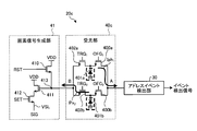
- FIG. 5 is a diagram illustrating a configuration of an example of the light receiving unit 40a according to the first embodiment.
- the light receiving section 40a includes two light receiving elements 401a and 401b each formed of, for example, a photodiode (PD).
- PD photodiode
- the light receiving element 401a has a cathode connected to the ground and an anode connected to the source of the transistor 400a formed by an N-type MOS transistor.
- the drain of the transistor 400a is connected to the address event detector 30.
- the gate of the transistor 400a the signal OFG 1 is supplied.
- Transistor 400a is signal OFG 1 is turned on at a high (High) state, the signal OFG 1 is turned off at a low (Low) state.
- Transistor 400a is in the ON state, the photocurrent Iph 1 output from the light receiving element 401a is supplied to the address event detection unit 30.
- the light receiving element 401b has a cathode connected to the ground and an anode connected to the source of the transistor 400b formed by an N-type MOS transistor.
- the drain of the transistor 400b is connected to the address event detector 30 in common with the drain of the transistor 400a described above.
- the gate of the transistor 400b the signal OFG 2 is supplied.
- Transistor 400b is the signal OFG 2 is turned on in a high state, the off at a low state.
- Transistor 400b is in ON state, the photocurrent Iph 2 output from the light receiving element 401b is supplied to the address event detection unit 30.
- the light receiving element 401a has lower sensitivity than the light receiving element 401b. That is, when the light receiving element 401a and the light receiving element 401b and the same amount of light is incident, a current value of the photocurrent Iph 1 output from the light receiving element 401a is of the photocurrent Iph 2 output from the light receiving element 401b It is smaller than the current value (Iph 1 ⁇ Iph 2 ).
- FIGS. 6A and 6B are diagrams illustrating an example of the pixel 20a including the light receiving elements 401a and 401b having different sensitivities. Note that, in FIGS. 6A and 6B, the light receiving elements 401a and 401b are described as PD 1 and PD 2, respectively.
- FIG. 6A is an example in which the areas of the light receiving portions in the light receiving elements 401a and 401b are made different to form a sensitivity difference.
- the area of the light receiving section of the light receiving element 401a is smaller than the area of the light receiving section of the light receiving element 401b.
- the light receiving element 401a performs less photoelectric conversion than the light receiving element 401a. Therefore, the light sensitivity of the light receiving element 401a is lower than that of the light receiving element 401b.
- FIG. 6B shows an example in which the light receiving elements 401a and 401b have the same configuration and the light receiving section has the same area, while a part (half in the example of FIG. 6B) of the light receiving section of the light receiving element 401a is shielded by a mask or the like. It is.
- the light applied to the light receiving element 401a is incident on the light receiving section in the opening area A, and is not incident on the light receiving section in the light shielding area B. Therefore, the areas of the light receiving portions of the light receiving elements 401a and 401b are substantially different, and the light sensitivity of the light receiving element 401a is lower than that of the light receiving element 401b, as in the example of FIG. 6A.
- FIG. 7 is a diagram schematically illustrating an example of wiring in the pixel array unit 110a according to the first embodiment.
- Drive circuit 113a generates a signal OFG 1 and OFG 2 under the control of the control unit 115, the generated these signals OFG 1 and OFG 2, supplied to each pixel 20a.
- the drive circuit 113a for each pixel 20a arranged in a two-dimensional lattice shape on the pixel array section 110a, and generates a signal OFG 1 and OFG 2 for each row.
- each pixel 20a is connected to the lower arbiter 112 on a row-by-row basis for transmitting and receiving requests and responses.
- each pixel 20a is connected to the column arbiter 111 on a column basis for transmitting and receiving a request and a response, and supplying an event detection signal indicating the detection of an event and address information.
- the column arbiter 111 supplies the event detection signal and the address information supplied from the pixel 20a to the control unit 115.
- the control unit 115 specifies a row to be switched between the high / low state of the signals OFG 1 and OFG 2 based on the event detection signal and the address information supplied from the column arbiter 111.
- Controller 115 an instruction of switching the high / low state of the signal OFG 1 and OFG 2 in a particular row, and supplies to the drive circuit 113a.
- Drive circuit 113a switches between the high / low state of signals OFG 1 and OFG 2 in the row in response to this instruction.
- the signal OFG 1 and OFG 2 is have been supplied in units of rows of pixels 20a included in the pixel array section 110a, which is not limited to this example.
- a signal OFG 1 and OFG 2 may be supplied collectively to all the pixels 20a included in the pixel array section 110a, the pixel array section 110a, a plurality of blocks including a predetermined number of pixels 20a
- the signal may be divided and the signals OFG 1 and OFG 2 may be supplied in block units.
- FIG. 8 is a diagram showing the configuration of the address event detection unit 30 applicable to the first embodiment in more detail.
- the address event detection unit 30 includes a current-voltage conversion unit 300, a buffer amplifier 310, a subtraction unit 320, and a quantizer 330.
- the current-voltage converter 300 includes transistors 301 and 303 using N-type MOS transistors and a transistor 302 using P-type MOS transistors.
- the description is given on the assumption that the light receiving element 401a is a photodiode.
- FIG. 8 shows only the light receiving element 401a among the light receiving elements 401a and 401b included in the light receiving section 40a, and omits the description of the transistor 400a for the sake of explanation.
- the source of the N-type transistor 301 is connected to the light receiving element 401a, and the drain is connected to the power supply terminal.
- the P-type transistor 302 and the N-type transistor 303 are connected in series between a power supply terminal and a ground terminal.
- a connection point between the drain of the transistor 302 and the drain of the transistor 303 is connected to the gate of the transistor 301 and the input terminal of the buffer amplifier 310.
- a predetermined bias voltage Vbs is applied to the gate of the transistor 302.
- the drains of the N-type transistors 301 and 303 are connected to the power supply side, and form source followers.
- the photocurrent output from the light receiving element 401a is converted into a logarithmic voltage signal by the two source followers connected in a loop. Further, the transistor 302 supplies a constant current to the transistor 303.
- Subtraction unit 320 includes capacitors 321 and 322 having capacitances C 1 and C 2 , a switch unit 323, and an inverter 324, respectively.
- Capacitor 322 is connected in parallel to inverter 324.
- the switch unit 323 switches a path connecting both ends of the capacitor 322 between an on state and an off state according to a row drive signal.
- Inverter 324 inverts the voltage signal input via capacitor 321.
- the inverter 324 supplies the inverted signal to the quantizer 330.
- the electric charge Q 2 stored in the capacitor 322 is expressed by the following equation (3), where the output voltage of the inverter 324 is V out .
- Q 2 ⁇ C 2 ⁇ V out (3)
- Equation (5) represents a subtraction operation of the voltage signal, and the gain of the subtraction result is a ratio C 1 / C 2 of the capacitance of the capacitors 321 and 322.
- the capacity C 1 of the capacitor 321 also preferably designed to have a small capacitance C 2 of the capacitor 322.
- the capacitance C 2 of the capacitor 322 is too small, there is a possibility that kTC noise increases, the noise characteristic deteriorates. Therefore, reduction of the capacitance C 2 of the capacitor 322 is limited to a range that can tolerate the noise.
- the address event detection unit 30 including a subtraction unit 320 is mounted on each of the pixels 20, the capacitance C 1 and C 2 of the capacitors 321 and 322, there is a restriction on the area. In consideration of these, the values of the capacitances C 1 and C 2 of the capacitors 321 and 322 are determined.
- the quantizer 330 detects three states of an up event, a down event, and no event detection using two thresholds of an ON threshold and an OFF threshold. Therefore, the quantizer 330 is called a 1.5-bit quantizer.
- FIG. 9 is a diagram for explaining the operation of the address event detection unit 30 shown in FIG.
- the horizontal axis represents time
- the vertical axis represents voltage.
- 9 shows an example of the output voltage Vp of the current-voltage converter 300.
- the lower part of FIG. 9 illustrates the state of the voltage V diff , which is the output voltage of the subtractor 320, corresponding to the change of the upper output voltage Vp.
- the voltage V diff corresponds to the voltage V out in the above equation (5).
- the OFF threshold and the ON threshold are thresholds for the voltage V diff for detecting a down event and an up event, respectively.
- the voltage V diff exceeds the OFF threshold in the positive direction, an up event is detected.
- the voltage V diff exceeds the ON threshold in the negative direction, a down event is detected. If the voltage V diff is less than the OFF threshold and greater than the ON threshold, it is determined that no event is detected.
- the output voltage Vp output from the current-to-voltage converter 300 is input to the subtractor 320 via the buffer amplifier. First, a case where the amount of light received by the light receiving element 401a increases and the output voltage Vp output from the current-voltage converter 300 increases will be described.
- the output voltage Vp from the time t 0 increases, at time t 1, it is assumed that the voltage V diff is a difference from the output voltage Vp at the time t 0 of the output voltage Vp exceeds the ON threshold in the negative direction.
- the quantizer 330 outputs an event detection signal indicating up event detection.
- the row drive circuit 110 switches the switch section 323 to the ON state, and the output of the subtraction section 320 is set to the reset level.
- the row drive circuit 110 switches the switch unit 323 to the off state immediately after setting the output of the subtraction unit 320 to the reset level.
- the address event detection unit 30 compares the difference between the output voltage Vp of the current-voltage conversion unit 300 with the ON threshold value and the OFF threshold value, as described above, to obtain an event detection signal corresponding to a change in the amount of light received by the light receiving element 401a. Can be output.
- the voltage Vp ′ is obtained by rewriting the change of the output voltage Vp of the current-voltage converter 300 in the lower part of FIG. 9, that is, according to the output of the quantizer 330. From the determination result based on the change in the voltage Vp ′ and the ON threshold value and the OFF threshold value based on the voltage Vdiff , the quantizer 330 determines, in other words, the rise and fall of the change in the voltage Vp ′ for each ON threshold value and OFF threshold value. Is detected.
- FIG. 10 is a diagram illustrating an example of the Vg-Id characteristic of the transistor 301, which is an N-type MOS transistor, used in the current-voltage converter 300 (see FIG. 8) according to the first embodiment.
- the horizontal axis represents the gate voltage Vg
- the vertical axis represents the drain current Id (ln) in logarithmic representation.
- the Vg-Id characteristic of the transistor 301 shifts from the OFF region to the sub-threshold region and further shifts from the sub-threshold region to the saturation region as the gate voltage Vg increases.
- the OFF region is a region where the drain current Id is substantially constant with an increase in the gate voltage Vg.
- the sub-threshold region is a region where the drain current Id increases logarithmically as the gate voltage Vg increases.
- the saturation region is a region where the drain current Id increases substantially linearly as the gate voltage Vg increases.
- the current-to-voltage converter 300 converts the photocurrent Iph output from the light receiving element 401a into a voltage by logarithmic conversion to obtain an output voltage Vp using the characteristics of the sub-threshold region. Therefore, a range 420 corresponding to the range of the gate voltage Vg in the sub-threshold region is a detection range of the photocurrent Iph output from the light receiving element 401a. As described above, the light detection range (dynamic range) of the address event detection unit 30 is limited to the current range of the sub-threshold region of the transistor that performs the current-voltage conversion.
- FIG. 11 is a diagram illustrating an example of input / output characteristics of the current-voltage converter 300 applicable to the first embodiment.
- the horizontal axis represents the photocurrent Iph output from the light receiving element 401a or 401b as a logarithm, and the vertical axis represents the output voltage Vp of the current-voltage converter 300. Note that FIG. 11 corresponds to a diagram in which the vertical axis and the horizontal axis of the graph of FIG. 10 are interchanged.
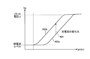
- characteristic lines PD 1 and PD 2 shows a characteristic example of light receiving elements 401a of the low sensitivity described with reference to FIG. 5, a characteristic example of the light receiving element 401b of the normal speed, respectively.
- the dark current level is a voltage level obtained by converting a dark current generated in the light receiving elements 401a and 401b into a voltage.
- the dark current level is the lower limit value of the output voltage Vp of the current-voltage converter 300.
- the light receiving element 401a of the low sensitivity the current value of the photocurrent Iph 1 is output when the light receiving element 401b in the same amount of normal sensitivity is incident, output from the light receiving element 401b the current value of the current Iph 2 smaller.
- the light-receiving element 401a of the low sensitivity even if light enters a large amount, the photocurrent Iph 1 is small is output. Therefore, the characteristic line PD 1 of the light receiving element 401a, to the characteristic line PD 2 of the light-receiving element 401b, shifts (to the right in FIG. 11) direction of larger photocurrent Iph.
- a current value a of the photocurrent Iph 1 by the light receiving element 401a is, the photocurrent Iph according to the light receiving element 401b It shifted to the larger side with respect to second current value b.
- light detection for detecting an address event is performed using both a low-sensitivity light receiving element 401a and a normal-sensitivity light receiving element 401b.
- FIGS. 12A and 12B are diagrams for explaining control for performing address event detection using the low-sensitivity light-receiving element 401a and the normal-sensitivity light-receiving element 401b according to the first embodiment.
- FIG. 12A shows an example in which an address event detection by the address event detection unit 30 based on the photocurrent Iph 1 output from the light receiving element 401a.
- a signal OFG 1 supplied to the gate of the transistor 400a and the high state the signal OFG 2 supplied to the gate of the transistor 400b and the low state.
- the transistor 400a is turned on, the transistor 400b is turned off, and the photocurrent Iph 1 output from the light receiving element 401a, the photoelectric current Iph 2 output from the light receiving element 401b, of the photocurrent Iph 1 is transistor
- the signal is supplied to the address event detection unit 30 via the signal 400a.
- FIG. 12B shows an example in which an address event detection by the address event detection unit 30 based on the photocurrent Iph 2 output from the light receiving element 401b.
- a signal OFG 1 supplied to the gate of the transistor 400a and a low state the signal OFG 2 supplied to the gate of the transistor 400b and the high state.
- the transistor 400a is turned off, the transistor 400b is turned on, the photocurrent Iph 1 output from the light receiving element 401a, the photoelectric current Iph 2 output from the light receiving element 401b, of the photocurrent Iph 2 the transistor
- the data is supplied to the address event detection unit 30 via the line 400b.
- Address event detection unit 30 thus, of the photocurrent Iph 1 and Iph 2, and outputs an event detection signal based on a signal OFG 1 and OFG photocurrent Iph det selected according to 2.
- FIG. 13 is a diagram illustrating an example of a configuration of the current-voltage converter 300a to which the limiter is applied according to the first embodiment.
- FIG. 13 omits the buffer amplifier 310, the subtraction unit 320, and the quantizer 330 in the address event detection unit 30 shown in FIG.
- the current-voltage converter 300a has a configuration in which a transistor 304, which is a P-type MOS transistor, is added as a limiter to the current-voltage converter 300 of FIG. More specifically, the source of the transistor 304 is connected to the output path of the event detection signal of the current-voltage converter 300a, that is, the connection point between each drain of the transistors 302 and 303 and the gate of the transistor 301, The drain of 304 is connected to ground.
- a transistor 304 which is a P-type MOS transistor
- the upper limit of the voltage value of the event detection signal output from the current-voltage converter 300a can be limited to a voltage corresponding to the limit voltage Lt.
- the description will be given on the assumption that the upper limit of the voltage value of the event detection signal output from the current-voltage converter 300a is limited to the limit voltage Lt.
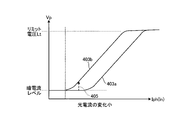
- FIG. 14 is a diagram illustrating an example of input / output characteristics of the current-voltage converter 300a according to the first embodiment.
- the horizontal axis represents the logarithm of the photocurrent Iph output from the light receiving element 401a or 401b
- the vertical axis represents the output voltage Vp of the current-voltage converter 300.
- the input / output characteristics of the current / voltage converter 300a are such that the output voltage Vp in the input / output characteristics of the current / voltage converter 300 in FIG. 11 is limited by the limit voltage Lt.
- the output voltage Vp usually based on the photocurrent Iph 2 of the light-receiving element 401b of sensitivity, corresponding to the voltage of the saturation point, the current value b of the photocurrent Iph 2 by the light receiving element 401b, is limited to the limit voltage Lt You.
- the photocurrent Iph det used for address event detection using the mechanism of address event detection process, the photocurrent Iph 1 output from the light receiving element 401a of the low sensitivity, It switched between photocurrent Iph 2 outputted from the light receiving element 401b of the normal speed.
- the switching process according to the first embodiment will be described with reference to FIGS.
- the signal OFG 1 is a high state, it is assumed that the photocurrent Iph 1 output from the light receiving element 401a of the low sensitivity are supplied to the address event detection section 30a.
- Figure 15 is a diagram showing an example of a variation of the photocurrent Iph 1 output from the light receiving element 401a of the low sensitivity.
- both ends of a change of the photocurrent Iph 1 is defined by a dark current level and limit voltage Lt.
- Figure 16 corresponds to a change of the photocurrent Iph 1 in FIG. 15 is a timing chart showing an example of processing in the solid-state imaging device 11a.
- a chart (a 1 ) shows an example of a change in the photocurrent Iph 1 output from the low-sensitivity light receiving element 401a (low-sensitivity PD).
- it is output photocurrent Iph 2 even in the light-receiving element 401b of the normal speed (normal sensitivity PD), showing an example of a variation of the photocurrent Iph 2, in the chart of FIG. 16 (b 1) .
- a chart (e 1 ) shows an example of an event detection signal output from the address event detection unit 30a.
- event detection signal corresponding to the change of the photocurrent Iph 1 of low sensitivity PD shown in chart (a 1), are output at time t 10, t 11 and t 12.
- Charts (c 1 ) and (d 1 ) show examples of arbitration for the event detection signal output from the pixel 20a including the low-sensitivity PD and the normal sensitivity PD in the low arbiter 112 and the column arbiter 111, respectively.
- the event detection signal shown in the chart (e 1 ) is selected.
- charts (f 1 ) and (g 1 ) show the states of the signals OFG 1 and OFG 2 , respectively. Initially, the signal OFG 1 is set to the high state and the signal OFG 2 is set to the low state, and the photocurrent Iph 1 output from the low-sensitivity PD shown in the chart (a 1 ) is supplied to the address event detection unit 30.
- the control unit 115 acquires the event detection signal from the column arbiter 111, based on the acquired event detection signal, predicts that the photocurrent Iph 1 in the low-sensitivity PD, and a variation of the photocurrent Iph 1.
- Control unit 115 when the amount of change predicted photocurrent Iph 1 exceeds a predetermined amount, switches low signal OFG 1 state, the signal OFG 2 in the high state (time t 13). Accordingly, the photocurrent Iph 2 normal sensitivity PD is supplied to the address event detection unit 30.
- the address event detection unit 30 detects a down event when the amount of change exceeds the OFF threshold in the positive direction, and detects an up event when the amount of change exceeds the ON threshold in the negative direction (see FIG. 9).
- the address event detection unit 30 detects an up event assuming that the amount of change has exceeded the OFF threshold in the positive direction, and outputs an event detection signal (time t 14 ).
- Column arbiter 111 and Roabita 112 selects an event detection signal at this time t 14.
- Control unit 115 acquires the event detection signal from the column arbiter 111 returns a signal OFG 1 to a high state (time t 15), returning the signal OFG 2 to a low state (time t 16). Thereafter, the address event detection unit 30 performs the address event detection by continuously using the low-sensitivity PD selected in the initial state (for example, at time t 17 ).
- FIGS. Figure 17 corresponds to Figure 15 described above, is a diagram illustrating an example of a change of the photocurrent Iph 1 output from the light receiving element 401a of the low sensitivity.
- the lower end of the change of the photocurrent Iph 1 it is hanging on the dark current level.
- the amount of change in light intensity that causes a change of the photocurrent Iph 1 may amount variation greater possibility shown in the variation photocurrent Iph 1.
- Figure 18 corresponds to a change of the photocurrent Iph 1 in FIG. 17 is a timing chart showing an example of processing in the solid-state imaging device 11a. Note that the meanings of the respective charts (a 2 ) to (g 2 ) in FIG. 18 are the same as those of the respective charts (a 1 ) to (g 1 ) of FIG. 16 described above, and thus description thereof will be omitted. Also in the example of FIG. 18, similarly to FIG. 16 described above, as shown in the chart (e 2 ), the event detection signal corresponding to the change in the photocurrent Iph 1 of the low-sensitivity PD is changed at time t 20 , It is output at t 21 and t 22.
- the signal OFG 1 is initially in the high state
- the signal OFG 2 is in the low state
- the low sensitivity PD shown in the chart (a 2 ) photocurrent Iph 1 to be output is supplied to the address event detection unit 30.
- control unit 115 similarly to the explanation in FIG. 16, based on the event detection signal acquired from the column arbiter 111, predicts the photocurrent Iph 1 in the low-sensitivity PD, and a variation of the photocurrent Iph 1.
- Control unit 115 when the amount of change predicted photocurrent Iph 1 exceeds a predetermined amount, switches low signal OFG 1 state, the signal OFG 2 in the high state (time t 23). Accordingly, the photocurrent Iph 2 normal sensitivity PD is supplied to the address event detection unit 30.
- the address event detection unit 30 determines that the amount of change does not exceed the ON threshold value and the OFF threshold value, and determines that no event is detected, and as illustrated in a range surrounded by a dotted line in FIG. Does not output event detection signal. Thereby, the low-sensitivity PD is excluded from the target of the address event detection, and the normal sensitivity PD is the target of the address event detection.
- the address event detection unit 30, performs address event detection based on the photocurrent Iph 2 normal sensitivity PD shown in chart (b 2) of FIG. 18, the amount of change in time t 24 is the OFF threshold A down event is detected as having exceeded the forward direction, and an event detection signal is output.
- Column arbiter 111 and Roabita 112 selects an event detection signal at this time t 24.
- the control unit 115 maintains the low state of the signal OFG 1 and the high state of the signal OFG 2 even if the event detection signal is obtained from the column arbiter 111, and the normal sensitivity switched from the low sensitivity PD at time t 23 .
- the address event is detected using the PD.
- the optical current Iph det used for address event detection, the photocurrent Iph 1 output from the low-sensitivity PD (light receiving element 401a), usually sensitivity PD (light receiving element 401b) outputs the control of switching between the photocurrent Iph 2, can be performed by utilizing the structure for the address event detection.
- the signal OFG 1 and OFG 2 are supplied in units of rows of pixels 20a included in the pixel array portion 110a. Therefore, in each pixel 20a, unable to hold the selection state by the signal OFG 1 and OFG 2.
- the selection state by the signals OFG 1 and OFG 2 for each pixel 20 a can be held.
- FIG. 19 is a diagram schematically illustrating an example of wiring in a pixel array unit 110b according to a modification of the first embodiment.
- the above-described pixels 20a are arranged in a two-dimensional lattice, and the terminals Tm 1 and Tm 2 of the switch 21 are connected to each pixel 20a.
- terminal Tm 1 of switch 21 is connected to the gate of transistor 400a in light receiving unit 40a included in pixel 20a
- terminal Tm 2 is connected to the gate of transistor 400b in light receiving unit 40a.
- the drive circuit 113b generates a signal OFG for each row under the control of the control unit 115, and supplies the generated signal OFG to each pixel 20a via a common terminal Tc of the switch 21 connected to each pixel 20a.
- the switch 21 selects one of the terminals Tm 1 and Tm 2 according to the selection signal SL supplied from the drive circuit 113b.
- the drive circuit 113b generates each selection signal SL corresponding to each pixel 20a under the control of the control unit 115, and supplies the selection signal SL to the switch 21 connected to each pixel 20a for each row. Note that FIG. 19 shows that a plurality of selection signals SL are supplied as the selection signal SLs.
- the selection state of the terminals Tm 1 and Tm 2 in each switch 21 according to a certain selection signal SL is held until the next selection signal SL is supplied.
- a photoelectric current Iph 1 by the light receiving element 401a of the low sensitivity, the optical current Iph 2 by the light receiving element 401b of the normal speed, the selected state can be maintained.
- the switch 21 is shown to be provided outside the pixel 20a, but this is not limited to this example, and the switch 21 may be provided inside the pixel 20a.
- the selection signal SL is supplied to each of the pixels 20a.
- the present invention is not limited to this example.
- a logic circuit for switching the terminals Tm 1 and Tm 2 of the switch 21 according to a specific bit string may be provided for each pixel 20a. By doing so, it is possible to reduce the number of signal lines for supplying the selection signal SLs.
- one switch 21 is connected to one pixel 20a, but this is not limited to this example, and one switch 21 can be shared by a plurality of pixels 20a.
- FIG. 20 is a diagram illustrating a configuration of an example of a pixel 20b according to the second embodiment.
- the pixel 20b includes a light receiving unit 40b and a current-voltage conversion unit 300.
- the current-voltage converter 300 has the same configuration as the current-voltage converter 300 described with reference to FIG. Note that the limiter (transistor 304) described with reference to FIG. 13 may be added to the current-voltage converter 300 in FIG.
- the light receiving unit 40b includes light receiving elements 401c and 401d having substantially the same sensitivity.
- the light receiving element 401c has a cathode connected to the ground and an anode connected to the source of the transistor 400a formed by an N-type MOS transistor.
- the drain of the transistor 400a is connected to a connection point where the source of the transistor 301 of the current-voltage converter 300 and the gate of the transistor 303 are connected.
- the gate of the transistor 400a, the signal OFG 1 is supplied.
- the light receiving element 401d has a cathode connected to the ground and an anode connected to the source of the transistor 400b formed by an N-type MOS transistor.
- the drain of the transistor 400b is connected to a connection point where the source of the transistor 301 of the current-voltage converter 300 and the gate of the transistor 303 are connected in common with the drain of the transistor 400a.
- the gate of the transistor 400b, the signal OFG 2 is supplied.
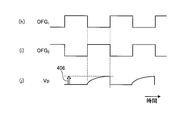
- FIG. 21 is a time chart illustrating an example of a driving method of the light receiving unit 40b according to the second embodiment.
- charts (h) and (i) show the states of the signals OFG1 and OFG2, respectively, and chart (j) shows the output voltage Vp output from the current-voltage converter 300.
- the control unit 115 acquires the output voltage Vp output from the current-voltage conversion unit 300 in synchronization with the switching timing, and sets the output voltage Vp 1 when the signal OFG 1 is in a high state and the signal OFG 2 to be high.
- the output voltage Vp 2 in the state is compared with the output voltage Vp 2 to obtain a difference 406 between the output voltages Vp 1 and Vp 2 .
- This photocurrent Iph 1 output from the light receiving element 401c corresponds to the process of obtaining a photoelectric current Iph 2 output from the light receiving element 401d, the difference.
- the control unit 115 treats the difference 406 as an event detection signal and analyzes the difference 406 in the control unit 115 or outside.
- FIGS. 22A, 22B, and 22C are diagrams illustrating an example of a configuration of light receiving elements 401c and 401d applicable to the second embodiment.
- FIG. 22A shows an example of a pixel 20b (a) in which light receiving elements 401c and 401d are arranged in parallel.
- information on the edge of the image can be obtained based on the difference 406.
- FIG. 22B shows an example of a pixel 20b (b) in which the light receiving elements 401c and 401d are arranged in parallel and adjacent to each other, and a portion adjacent to the light receiving elements 401c and 401d is shielded by using a light shielding pattern 407.
- the light shielding pattern 407 is, for example, a metal light shielding pattern.
- the light incident on the pixel 20b (b) is received by the light receiving elements 401c and 401d from the openings not shielded by the light shielding pattern 407.
- FIG. 23 is a diagram schematically showing how light is incident on the light receiving elements 401c and 401d in the pixel 20b (b) of FIG. 22B.
- a light-shielding pattern 407 is provided on the light receiving elements 401c and 401d arranged adjacent to each other, and a lens 440 is provided corresponding to the pixel 20b (b).
- the lens 440 is, for example, an OCL (On Chip Lense).
- the light incident on the lens 440 is applied to the pixel 20b (b), and this light is shielded by the light-shielding pattern 407, and is located on the right side of the light receiving element 401c and the left side of the light receiving element 401d in FIG. Is not incident.
- Light 409a on the left side of the lens 440 in FIG. 23 is incident on the left side of the light receiving element 401c which is not shielded.
- Light 409b on the right side is incident on the unshielded right side of the light receiving element 401d.
- the pixel 20b (b) can be used as an image plane phase difference pixel.
- the image plane phase difference pixel is usually formed by stacking an aperture filter having an opening on the left half of the light receiving surface of the light receiving element, for example, and opening the pixel on the right half of the light receiving surface of the other light receiving element. And a pixel on which the aperture filter is stacked, as a set, and distance measurement is performed based on a phase difference of light received by the two pixels.
- FIG. 22B it is possible to form an image plane phase difference pixel with one pixel 20b (b).
- FIG. 22C shows an example of a pixel 20b (c) in which a polarization filter 408 is provided for the light receiving elements 401c and 401d with different polarization directions.
- the polarizing filter 408 can be formed by a metal light-shielding pattern in which a number of slits through which light passes are provided in parallel. As described above, by making the polarization directions of the light receiving elements 401c and 401d included in the pixel 20b (c) different, the polarization can be detected by one pixel 20b (c).
- the control unit 115 the signal OFG 1 is the time of transition from a high state to a low state, to obtain the output voltage Vp 1 of the photocurrent Iph output from the light receiving element 401c is converted.
- the signal OFG 2 is shifted to a high state.
- Control unit 115, the signal OFG 2 is the time of transition from the high state to a low state, to obtain the output voltage Vp 2 photocurrent Iph output from the light receiving element 401d is converted.
- the control unit 115 calculates a difference 406 between the output voltages Vp 1 and Vp 2 , and it is assumed that an address event is detected when the difference 406 exceeds an ON threshold or an OFF threshold in a predetermined direction.
- the pixel 20b including the light receiving elements 401c and 401d having the same sensitivity can be used for various uses.
- the address event detection is performed based on the change in the photocurrent Iph output from the light receiving element.
- an address event is detected by further using a pixel signal corresponding to the absolute value of the photocurrent Iph output from the light receiving element.
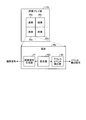
- FIG. 24 is a block diagram illustrating a configuration of an example of the solid-state imaging device according to the third embodiment, which corresponds to the solid-state imaging device 11 described with reference to FIG. 24,
- the solid-state imaging device 11c includes a pixel array unit 110c, a column arbiter 111, a low arbiter 112, a row driving circuit 113c, a signal processing unit 114c, a control unit 115, and a column driving circuit 116.
- the row driving circuit 113c includes the function of the driving circuit 113a shown in FIG.
- the pixel array section 110c has a plurality of pixels arranged in a two-dimensional lattice like the pixel array section 110a described with reference to FIG.
- Each of the pixels has a plurality of light receiving elements for outputting a photocurrent Iph corresponding to the received light, and an address event for detecting an address event based on a change amount of the light current Iph output from the plurality of light receiving elements.
- a detection unit; and a pixel signal generation unit that generates a pixel signal which is an analog signal of a voltage corresponding to the absolute value of the photocurrent Iph.
- the row driving circuit 113c has a function of driving each of the pixels and outputting a pixel signal to the column driving circuit 116, in addition to the function of the driving circuit 113a of FIG.
- the column driving circuit 116 includes an AD (Analog to digital) converter for each column, and a driving circuit for scanning the AD converter for each column in the row direction.
- the AD converter for each column is called a column ADC (AD converter).
- the column drive circuit 116 scans the column ADC in the row direction, and outputs a pixel signal converted into a digital signal by each AD converter in row units.
- the pixel signal output from the column driving circuit 116 is supplied to the signal processing unit 114c.
- the signal processing unit 114c performs predetermined signal processing such as CDS (Correlated Double Sampling) processing and AGC (Auto Gain Control) processing on the digital pixel signal supplied from the column driving circuit 116. Further, signal processing such as image recognition processing is performed on the event detection signal supplied from the column arbiter 111. The signal processing unit 114c supplies the data indicating the processing result and the event detection signal to the storage unit 120.
- predetermined signal processing such as CDS (Correlated Double Sampling) processing and AGC (Auto Gain Control) processing
- CDS Correlated Double Sampling
- AGC Automatic Gain Control
- FIG. 25 is a block diagram illustrating a configuration of an example of a pixel array unit 110c according to the third embodiment.
- the pixel array unit 110c includes a plurality of pixels 20c arranged in a two-dimensional lattice.
- each pixel 20c includes an address event detecting unit 30, a light receiving unit 40c, and a pixel signal generating unit 41.
- the light receiving section 40c includes a plurality of light receiving elements, and photoelectrically converts incident light to generate a photocurrent Iph.
- the light receiving unit 40c supplies the generated photocurrent Iph to one of the pixel signal generation unit 41 and the address event detection unit 30 under the control of the row driving circuit 113c.
- the address event detection unit 30 Upon detecting the occurrence of the address event, the address event detection unit 30 requests the column arbiter 111 and the low arbiter 112 to transmit an event detection signal indicating the occurrence of the address event. When receiving a response to this request from the column arbiter 111 and the low arbiter 112, the address event detection unit 30 supplies an address detection signal to the row drive circuit 113c and the signal processing unit 114c.
- the address event detection unit 30 includes the current-voltage conversion unit 300a described with reference to FIG. 13 and which limits the upper limit of the output voltage Vp to the limit voltage Lt by the limiter.
- the pixel signal generation unit 41 generates a signal of a voltage corresponding to the photocurrent Iph supplied from the light receiving unit 40c as a pixel signal.
- the pixel signal generation unit 41 supplies the generated pixel signal to the column driving circuit 116 via a vertical signal line.
- FIG. 26 is a diagram illustrating a configuration of an example of a pixel 20c according to the third embodiment.
- the light receiving section 40c includes, for example, two light receiving elements 401a and 401b each formed of, for example, a photodiode, and transistors 400a, 400b, 402a, and 402b, which are N-type MOS transistors.
- the pixel signal generation unit 41 includes a floating diffusion layer 413, and a reset transistor 410, an amplification transistor 411, and a selection transistor 412, each of which is an N-type MOS transistor.
- the light receiving element 401a has a cathode connected to the ground, and an anode connected to the source of the transistor 400a formed of an N-type MOS transistor and the drain of the transistor 402a formed of an N-type MOS transistor.
- the drain of the transistor 400a is connected to the address event detector 30.
- the source of the transistor 402a is connected to the floating diffusion layer 413 in the pixel signal generator 41.
- Transistor 400a is signal OFG 1 is turned on in a high state, signal OFG 1 is turned off in a low state.
- the gate of the transistor 400b, the signal OFG 2 is supplied.
- Transistor 400b is the signal OFG 2 is turned on in a high state, signal OFG 2 is turned off in a low state.
- Transistor 400a is in the ON state, the photocurrent Iph 1 output from the light receiving element 401a is supplied to the address event detection unit 30.
- the transistor 400b is in ON state, the photocurrent Iph 2 output from the light receiving element 401b is supplied to the address event detection unit 30.
- Transistor 402a is signal TRG 1 is turned on in a high state, signal OFG 1 is turned off in a low state.
- the gate of the transistor 402b, the signal TRG 2 is supplied.
- Transistor 402b is the signal TRG 2 is turned on in a high state, signal TRG 2 is turned off in a low state.
- Transistor 402a is in the ON state, the photocurrent Iph 1 output from the light receiving element 401a is supplied to the pixel signal generation section 41.
- the transistor 402b is in ON state, the photocurrent Iph 2 output from the light receiving element 401b is supplied to the pixel signal generation section 41.
- the floating diffusion layer 413 accumulates charges and generates a voltage corresponding to the amount of the accumulated charges.
- the reset transistor 410 initializes the charge amount of the floating diffusion layer 413 according to a reset signal RST supplied from the row drive circuit 113c.
- the amplification transistor 411 amplifies the voltage of the floating diffusion layer 413.
- the selection transistor 412 outputs the voltage signal amplified by the amplification transistor 411 as a pixel signal SIG to the column driving circuit 116 via the vertical signal line VSL according to the selection signal SEL from the row driving circuit 113c.
- the sensitivity of the light receiving element 401a is lower than that of the light receiving element 401b.
- the light receiving element 401a is referred to as a low sensitivity PD and the light receiving element 401b is referred to as a normal sensitivity PD as appropriate.
- FIG. 27 is a diagram schematically illustrating an example of wiring in a pixel array unit 110c according to the third embodiment. Similar to the drive circuit 113a of the pixel array unit 110a according to the first embodiment described with reference to FIG. 7, row drive circuit 113c is controlled to generate a signal OFG 1 and OFG 2 in accordance with the control unit 115, to generate These signals OFG 1 and OFG 2 are supplied to each pixel 20c. In the example of FIG. 27, the row drive circuit 113c, for each pixel 20c arranged in a two-dimensional lattice shape on the pixel array unit 110c, and generates a signal OFG 1 and OFG 2 for each row.
- Row drive circuit 113c further generates a signal TRG 1 and TRG 2 under the control of the control unit 115, the generated these signals TRG 1 and TRG 2, supplied to each pixel 20c.
- the row drive circuit 113c for each pixel 20c arranged in a two-dimensional lattice shape on the pixel array unit 110c, and generates a signal TRG 1 and TRG 2 for each row.
- the vertical signal line VSL of each pixel 20c is connected to the column drive circuit 116 for each column of each pixel 20c arranged in the pixel array unit 110c.
- the row drive circuit 113c further arranges the above-described reset signal RST and selection signal SEL in the pixel array unit 110c in a two-dimensional grid pattern under the control of the control unit 115. Is generated for each row for each pixel 20c. The row drive circuit 113c supplies the generated reset signal RST and selection signal SEL to each pixel 20c.
- FIGS. 28A and 28B are diagrams for describing control of the light receiving unit 40c according to the third embodiment.
- Figure 28A shows an example of a case where the address events detected by the address event detection unit 30 based on the photocurrent Iph 1 output from the light receiving element 401a is a low-sensitivity PD.
- a signal OFG 1 supplied to the gate of the transistor 400a and the high state the signal OFG 2 supplied to the gate of the transistor 400b and the low state.
- a signal TRG 1 supplied to the gate of the transistor 402a and a low state the signal TRG 2 supplied to the gate of the transistor 402b and the high state.
- the transistor 400a is turned on, the transistor 400b is turned off, the transistor 402a is turned off, and the transistor 402b is turned on.
- Photocurrent Iph 1 output from the light receiving element 401a is low sensitivity PD
- the photoelectric current Iph 2 output from the light receiving element 401b is generally sensitive PD
- the optical current Iph 2 is supplied to the pixel signal generating section 41 via the transistor 402b.
- Figure 28B shows an example of a case where the address events detected by the address event detection unit 30 based on the photocurrent Iph 2 output from the light receiving element 401b is generally sensitive PD.
- a signal OFG 1 supplied to the gate of the transistor 400a and a low state the signal OFG 2 supplied to the gate of the transistor 400b and the high state.
- a signal TRG 1 supplied to the gate of the transistor 402a and the high state the signal TRG 2 supplied to the gate of the transistor 402b and the low state.
- the transistor 400a is turned off, the transistor 400b is turned on, the transistor 402a is turned on, and the transistor 402b is turned off.
- Photocurrent Iph 1 output from the light receiving element 401a is low sensitivity PD
- the photoelectric current Iph 2 output from the light receiving element 401b is generally sensitive PD
- the optical current Iph 2 is supplied to the pixel signal generating section 41 via the transistor 402a.
- FIG. 29 is a timing chart illustrating an example of processing in the solid-state imaging device 11c according to the third embodiment.
- charts (k) and (n) show examples of the reset signal RST and the selection signal SEL generated in the row drive circuit 113c.
- Chart (o) shows an example of the voltage of the pixel signal on the vertical signal line VSL.
- charts (l) and (m) show examples of signals TRG 1 and TRG 2 generated in row driving circuit 113c
- charts (s) and (t) show signals in row driving circuit 113c.
- An example of generated signals OFG 1 and OFG 2 is shown.
- chart (r) shows an example of an event detection signal output from the address event detection unit 30.
- Charts (p) and (q) show examples of arbitration for the event detection signal shown in chart (r) in the lower arbiter 112 and the column arbiter 111, respectively. In each of the high states, the event detection signal shown in the chart (r) is selected.
- the signal OFG 1 is set to a high state and the signal OFG 2 is set to a low state as an initial state, and the photocurrent Iph 1 output from the low-sensitivity PD is supplied to the address event detection unit 30.
- the amount of change in the photocurrent Iph 1 in the low-sensitivity PD exceeds a predetermined amount, at time t 30, event detection signal from the address event detection section 30 is outputted.
- Control unit 115 acquires the event detection signal from the column arbiter 111, in accordance with the acquired event detection signal, instructs the row drive circuit 113c to a signal OFG 1 and a low state. Row drive circuit 113c, in accordance with this instruction, the signal OFG 1 and a low state (time t 31).
- Row drive circuit 113c in accordance with an instruction from the control unit 115, at time t 40, the reset signal RST and a signal TRG 1 as high, resetting the low sensitivity PD (light receiving element 401a) and the floating diffusion layer 413. Additionally, the row drive circuit 113c in accordance with an instruction from the control unit 115, at time t 41, the reset signal RST and a signal TRG 2 as a high state to reset the normal sensitivity PD (light receiving element 401b) and the floating diffusion layer 413.
- the period 510 including a time t 40 and t 41 are the sequence of the exposure start in the voltage reading operation of the pixel signal SIG.
- the selection signal SEL is kept in the low state, so that the pixel signal SIG is not output to the vertical signal line VSL.
- the row drive circuit 113c in accordance with an instruction from the control unit 115, starts the output of a selection signal SEL to the high state, to the vertical signal line VSL of the pixel signal SIG Let it. Row drive circuit 113c is maintained at a high state of the selection signal SEL, to the point t 49 the CDS readout is terminated due to normal sensitivity PD (light receiving element 401b).
- Pixel signal SIG 1 based on the photocurrent Iph 1 output from the low-sensitivity PD (light receiving element 401a) via the vertical signal line VSL supplied to the column drive circuit 116, CDS readout of low sensitivity PD is performed (period 511a ).
- the row drive circuit 113c at time t 47 immediately after the time t 46 to CDS reading less sensitive PD is completed, the reset signal RST to high state, the signal TRG 2 and high state at time t 48.
- the period 511 including the periods 511a and 511b is a reading sequence in the voltage reading operation of the pixel signal SIG.
- the row drive circuit 113c, the signal TRG 1 from the time t 40, which is a high state in the period 510, and time 520a to the point t 44 to signal TRG 1 is set to the high state in the period 511
- a period 510 from the time t 41 to signal TRG 2 is a high state
- time 520b signal TRG 2 is up to the time t 48, which is a high state in the period 511
- the exposure time of the low-sensitivity PD light receiving element 401a
- the exposure time of the normal sensitivity PD light receiving element 401b
- the row drive circuit 113c sets the selection signal SEL to a low state, and stops the output of the pixel signal SIG from the pixel signal generation unit 41.
- Control unit 115 the column driver circuit 116, the pixel signal SIG 1 read in the period 511a, and the pixel signals read out in the period 511b acquires the SIG 2.
- Control unit 115 based on these pixel signals SIG 1 and SIG 2 obtained, the photocurrent Iph 1 low sensitivity PD (light receiving element 401a), usually sensitivity PD of the photocurrent Iph 2 of (light-receiving element 401b),
- the address event detector 30 selects a photocurrent Iph det used for address event detection.
- control unit 115 is normally a photoelectric current Iph 2 sensitivity PD, is assumed to be selected as the photocurrent Iph det used for address event detection in the address event detection unit 30.
- Row drive circuit 113c in accordance with an instruction from the control unit 115 in accordance with this selection, at time t 32, a low signal OFG 1 state, the signal OFG 2 to a high state, output from the normal sensitivity PD (light receiving element 401b) that to supply the optical current Iph 2 to address event detection unit 30.
- control unit 115 fixes the timing at which the address event detection unit 30 executes the address event detection (indicated by the dotted frame in FIG. 29), and keeps the address event detection unit 30 detecting the address event fixed. It is controlled to be executed periodically. That is, one cycle of the address event detection execution includes the pixel signal readout operation in the periods 510 and 511 and the address event detection based on the readout operation.
- FIGS. 30 and 31 are diagrams for explaining a method of switching between the low-sensitivity PD and the normal sensitivity PD based on the voltage difference according to the third embodiment.
- FIGS. 30 and 31 correspond to FIG. 14 described above, and the meanings of the horizontal axis and the vertical axis, and the characteristic lines 403a and 403b are common to FIG. Is omitted.
- the address event detection unit 30 uses the photocurrent Iph det normal sensitivity PD (light receiving element 401b) low from the optical current Iph 2 output by the sensitivity PD (light receiving element 401a) is shows an example of the operation of switching to the photocurrent Iph 1 to be output.
- the control unit 115 determines whether or not the amount of light is increasing, for example, based on the pixel signal SIG read in the period 511 in FIG.
- the present invention is not limited thereto, and the control unit 115 may determine an increase in the amount of light based on the output voltage Vp of the current-voltage conversion unit 300a included in the address event detection unit 30.
- the control unit 115 determines whether or not the output voltage Vp of the current-voltage conversion unit 300a included in the address event detection unit 30 has entered a limit area based on the limit voltage Lt. If the control unit 115 determines that the output voltage Vp has entered the limit area in step S11, for example, the photocurrent used by the address event detection unit 30 for detecting the address event is synchronized with the detection of the up event by the address event detection unit 30. the Iph det, acquires the output voltage Vp is switched to the photocurrent Iph 1 low sensitivity PD.
- the control unit 115 compared to the photocurrent Iph 1 by the output voltage Vp of the obtained low-sensitivity PD (the voltage Vp low), the output voltage Vp used for the determination in step S11 (the voltage Vp nml) I do.
- the control unit 115 sets the signal OFG 1 to a high state and the signal OFG 2 to a low state, and the address event detection unit 30 detects the address event.
- the address event detection unit 30 uses the photocurrent Iph det low sensitivity PD (light receiving element 401a) Normal sensitivity from the photocurrent Iph 1 which is output PD (light receiving element 401b) is shows an example of the operation of switching to the photocurrent Iph 2 to be output.
- the signal OFG 1 is initially in a high state
- the signal OFG 2 is in a low state
- the photocurrent Iph 1 of the low-sensitivity PD is selected as the photocurrent Iph det used by the address event detection unit 30. I do.
- step S20 a decrease in the amount of light received by the pixel 20c is detected based on, for example, the pixel signal SIG read in the period 511 in FIG.
- the control unit 115 determines whether or not the output voltage Vp of the current-voltage conversion unit 300a included in the address event detection unit 30 has entered a dark current region based on the dark current level. If the control unit 115 determines that the output voltage Vp has entered the dark current region in step S21, for example, the light used by the address event detection unit 30 for detecting the address event is synchronized with the detection of the down event by the address event detection unit 30. the current Iph det, is switched to the photocurrent Iph 2 normal sensitivity PD acquires the output voltage Vp.
- the control unit 115 compares the acquired normal sensitivity PD of the photocurrent Iph 2 by the output voltage Vp (voltage Vp nml), and an output voltage Vp (voltage Vp low) used in the determination in step S21. As a result of the comparison, if the difference between the voltage Vp nml and the voltage Vp low is equal to or less than a predetermined value, the control unit 115 sets the signal OFG 1 to a low state, sets the signal OFG 2 to a high state, and causes the address event detection unit 30 to detect an address event. the photocurrent Iph det used for, switching from the photocurrent Iph 1 to the photocurrent Iph 2 (step S22).
- FIG. 32 is a flowchart illustrating an example of the switching operation of the photocurrent Iph when the amount of light received by the pixel 20c is increased according to the third embodiment described with reference to FIG.
- the signal OFG 1 is low
- the signal OFG 2 is a high state
- the photocurrent of normal sensitivity PD photocurrent Iph det using address event detection unit 30 in the address event detection shall Iph 2 is selected.
- step S100 the control unit 115 determines whether or not the amount of light received by the pixel 20c has increased based on, for example, the pixel signal SIG. If control unit 115 determines that the number has not increased (step S100, “No”), control unit 115 returns the process to step S100. On the other hand, when the control unit 115 determines that the amount of light received by the pixel 20c is increasing (step S100, “Yes”), the control unit 115 shifts the processing to step S101.
- step S101 the control unit 115 determines whether or not the output voltage Vp (voltage Vp nml ) of the current / voltage conversion unit 300a has entered the limit area.
- step S101 determines that the voltage Vp nml is not in the limit area (step S101, “No”)
- the process returns to, for example, step S100.
- step S101 determines that voltage Vp nml is within the limit area (step S101, “Yes”)
- control unit 115 shifts the processing to step S102.
- step S102 the control unit 115 acquires the voltage Vp nml based on the photocurrent Iph 2 normal sensitivity PD.
- step S103 the control unit 115, the signal OFG 1 a high state, the signal OFG 2 to a low state, a photocurrent Iph that is supplied to the address event detection unit 30, switches to the photocurrent Iph 1 low sensitivity PD .
- step S104 the control unit 115 acquires the voltage Vp low based on the photocurrent Iph 1 low sensitivity PD.
- step S105 the control unit 115, for example step S100, in synchronization with the detected up event based on the photocurrent Iph 2 normal sensitive PD during the step S101, the voltage Vp nml acquired in step S102, step The difference from the voltage Vp low acquired in S104 is detected.
- control unit 115 determines whether or not the difference detected in step S105 is equal to or smaller than a predetermined value. When determining that the difference is equal to or smaller than the predetermined value (step S106, “Yes”), control unit 115 shifts the processing to step S107. In step S107, the control unit 115, a high signal OFG 1 state, the signal OFG 2 and a low state, the address event detection section 30 as the photocurrent Iph det used for address event detection, the photocurrent Iph 1 low sensitivity PD select.
- control unit 115 shifts the processing to step S108.
- step S108 the control unit 115 maintains the state of the signal OFG 1 and OFG 2, the address event detection section 30 as the photocurrent Iph det used for address event detection, selecting a photocurrent Iph 2 normal sensitivity PD.
- step S107 or S108 ends, a series of processing in the flowchart in FIG. 32 ends.
- FIG. 33 is a flowchart illustrating an example of the operation of switching the photocurrent Iph when the amount of light received by the pixel 20c is reduced according to the third embodiment described with reference to FIG.
- the signal OFG 1 is set to the high state and the signal OFG 2 is set to the low state, and the photocurrent Iph det of the low-sensitivity PD is used by the address event detection unit 30 as the photocurrent Iph det used for address event detection. shall Iph 1 is selected.
- step S200 the control unit 115 determines whether or not the amount of light received by the pixel 20c has decreased based on, for example, the pixel signal SIG. If control unit 115 determines that the number has not decreased (step S200, “No”), control unit 115 returns the process to step S200. On the other hand, when the control unit 115 determines that the amount of light received by the pixel 20c is decreasing (step S200, “Yes”), the control unit 115 shifts the processing to step S201.
- step S201 the control unit 115 determines whether the output voltage Vp (voltage Vp low ) of the current-voltage conversion unit 300a has entered the dark current region.
- step S201 the control unit 115 determines that the voltage Vp low is not in the dark current region (step S201, “No”), the process returns to, for example, step S200.
- step S201 “Yes”
- step S202 the control unit 115 shifts the processing to step S202.
- step S202 the control unit 115 acquires the voltage Vp Low8 based on the photocurrent Iph 1 low sensitivity PD.
- step S203 the control unit 115, the signal OFG 1 in the low state, the signal OFG 2 to a high state, a photocurrent Iph that is supplied to the address event detection unit 30, switches to the photocurrent Iph 2 normal sensitivity PD .
- step S204 the control unit 115 acquires the voltage Vp nml based on the photocurrent Iph 2 normal sensitivity PD.
- step S205 the control unit 115, for example, step S200, in synchronization with the detected down event on the basis of the photocurrent Iph 1 of low sensitivity PD during the step S201, the voltage Vp low acquired in step S202, step The difference from the voltage Vp nml acquired in S204 is detected.
- control unit 115 determines whether or not the difference detected in step S205 is equal to or smaller than a predetermined value. When determining that the difference is equal to or smaller than the predetermined value (step S206, “Yes”), control unit 115 shifts the processing to step S207. In step S207, the control unit 115, the signal OFG 1 in the low state, the signal OFG 2 to a high state, photocurrent Iph det using address event detecting unit 30 is the address event detection, the normal sensitivity PD photocurrent Iph 2 select.
- step S206 determines that the difference exceeds the predetermined value in step S206 (step S206, “No”), the process proceeds to step S208.
- step S208 the control unit 115 maintains the state of the signal OFG 1 and OFG 2, the address event detection section 30 as the photocurrent Iph det used for address event detection, selecting the photocurrent Iph 1 low sensitivity PD.
- step S207 or S208 ends, a series of processing in the flowchart in FIG. 33 ends.
- the amount of light received by the pixel 20c is determined based on the pixel signal SIG, and based on the determination result, the photocurrent Iph det used by the address event detection unit 30 for detecting the address event is determined. They are selected from the photocurrent Iph 1 and Iph 2. Therefore, the process of selecting the photocurrent Iph det from the photocurrent Iph 1 and Iph 2, can be performed with higher accuracy.
- a control unit includes: A solid-state imaging device that controls the switching by the switching unit.
- the control unit includes: The solid-state imaging device according to (1), wherein the switching is controlled based on a change amount of a light amount applied to the pixel.
- the pixel is A generating unit that generates a pixel signal based on an absolute value of the first photocurrent or the second photocurrent,
- the control unit includes: The solid-state imaging device according to (1) or (2), wherein the switching is controlled based on the pixel signal.
- the control unit includes: Further controlling the switching based on the amount of change in the amount of light applied to the pixel, The solid-state imaging device according to (3), wherein the switching control based on the pixel signal and the switching control based on a change amount of the light amount are repeatedly executed in a constant cycle.
- the conversion unit Including a limiter for setting an upper limit value of the converted voltage, The switching unit includes: The solid-state imaging device according to any one of (1) to (4), wherein the switching is controlled based on a voltage converted by the conversion unit and a voltage range defined based on the upper limit.
- the control unit includes: When the first photocurrent is equal to or less than a predetermined value, the switching is controlled such that the current to be converted into a voltage by the conversion unit is switched from the first photocurrent to the second photocurrent.
- the solid-state imaging device according to any one of (5).
- the first light receiving element and the second light receiving element have equivalent sensitivity,
- the control unit includes: The solid-state imaging device according to (1), wherein the switching is controlled in a time-division manner.
- the detection unit The solid-state imaging device according to (7), wherein the event is detected based on a difference between the first photocurrent and the second photocurrent.
- the solid-state imaging device according to (7) or (8), wherein the light receiving state of the first light receiving element is different from the light receiving state of the second light receiving element.
- the solid-state imaging device according to (9), wherein different light blocking patterns are provided for the first light receiving element and the second light receiving element.
- the switching unit includes: The solid-state imaging device according to any one of (1) to (10), wherein the state in which the switching is controlled is held for each of the pixels.
- a switching step in which a switching unit included in the pixel switches a current to be converted into a voltage by the conversion step between the first photocurrent and the second photocurrent; And a control step of controlling the switching step.
Abstract
This solid-state imaging element is provided with a plurality of pixels (20a) arrayed in a 2-dimensional lattice, and a control unit (115). The pixels include: a first light-receiving element (401a) which outputs a first optical current corresponding to received light; a second light-receiving element (401b) which outputs a second optical current corresponding to received light; a conversion unit (300) which converts a current into a voltage; an output unit (320, 330) which detects an event on the basis of a change in the voltage obtained by conversion by the conversion unit, and outputs a detection signal indicating a detection result of the detection; and a switch unit (113a) which performs switching to switch the current to be converted into voltage by the conversion unit between the first optical current and the second optical current. The control unit controls the switching by the switch unit.
Description
本発明は、固体撮像素子、固体撮像素子の制御方法および電子機器に関する。
The present invention relates to a solid-state imaging device, a method for controlling the solid-state imaging device, and an electronic apparatus.
CMOS(Complementary Metal Oxide Semiconductor)などを用いた固体撮像装置において、画素アドレス毎に、その画素における受光素子が受光した光量が閾値を超えた旨をアドレスイベントとしてリアルタイムに検出する検出回路を画素毎に設けた、非同期型の固体撮像素子が提案されている(例えば特許文献1)。このように、画素毎にアドレスイベントを検出する固体撮像素子は、DVS(Dynamic Vision Sensor)と呼ばれる。
In a solid-state imaging device using CMOS (Complementary Metal Oxide Semiconductor) or the like, for each pixel address, a detection circuit that detects in real time that an amount of light received by a light receiving element in the pixel exceeds a threshold as an address event is provided for each pixel. An asynchronous solid-state imaging device provided has been proposed (for example, Patent Document 1). Such a solid-state image sensor that detects an address event for each pixel is called a DVS (Dynamic Vision Sensor).
このDVSのような非同期型の固体撮像素子を用いることで、既存の、垂直同期信号などの同期信号に同期した画像データを撮像する同期型の固体撮像素子を用いる場合に対して、より高速な応答が可能となる。そのため、非同期型の固体撮像素子のより多様な活用方法が求められている。
By using an asynchronous solid-state imaging device such as DVS, a higher speed can be achieved compared to a case where an existing synchronous solid-state imaging device that captures image data synchronized with a synchronization signal such as a vertical synchronization signal is used. Response is possible. Therefore, there are demands for more various methods of utilizing asynchronous solid-state imaging devices.
本開示は、アドレスイベントの検出を行う固体撮像素子をより多様に活用可能とすることを目的とする。
The present disclosure is intended to make it possible to use a solid-state imaging device that detects an address event more variously.
本開示に係る固体撮像素子は、2次元格子状に配列された複数の画素と、制御部と、を備え、画素は、受光した光に応じた第1の光電流を出力する第1の受光素子と、受光した光に応じた第2の光電流を出力する第2の受光素子と、電流を電圧に変換する変換部と、変換部により変換された電圧の変化に基づきイベントを検出し、検出による検出結果を示す検出信号を出力する出力部と、変換部により電圧に変換する電流を第1の光電流と第2の光電流とで切り替える切り替えを行う切替部と、を含み、制御部は、切替部による切り替えを制御する。
A solid-state imaging device according to an embodiment of the present disclosure includes a plurality of pixels arranged in a two-dimensional lattice and a control unit, and the pixel outputs a first photocurrent corresponding to the received light. An element, a second light receiving element that outputs a second photocurrent according to the received light, a conversion unit that converts the current into a voltage, and an event detected based on a change in the voltage converted by the conversion unit. A control unit including: an output unit that outputs a detection signal indicating a detection result by the detection; and a switching unit that switches a current to be converted into a voltage by the conversion unit between the first photocurrent and the second photocurrent. Controls switching by the switching unit.
以下、本開示の実施形態について、図面に基づいて詳細に説明する。なお、以下の各実施形態において、同一の部位には同一の符号を付することにより、重複する説明を省略する。
Hereinafter, embodiments of the present disclosure will be described in detail with reference to the drawings. In the following embodiments, the same portions will be denoted by the same reference numerals, and redundant description will be omitted.
[実施形態]
(各実施形態に適用可能な電子機器の構成例)
図1は、各実施形態に係る固体撮像素子を適用した電子機器としての撮像装置の一例の構成を概略的に示す図である。図1において、撮像装置1は、光学系10と、固体撮像素子11と、記憶部12と、制御部13と、を含む。光学系10は、1以上のレンズと、オートフォーカス機構および絞り機構などの各機構と、を含み、被写体からの光を固体撮像素子11の受光面に導く。 [Embodiment]
(Configuration Example of Electronic Apparatus Applicable to Each Embodiment)
FIG. 1 is a diagram schematically illustrating a configuration of an example of an imaging device as an electronic apparatus to which the solid-state imaging device according to each embodiment is applied. In FIG. 1, theimaging device 1 includes an optical system 10, a solid-state imaging device 11, a storage unit 12, and a control unit 13. The optical system 10 includes one or more lenses and respective mechanisms such as an autofocus mechanism and an aperture mechanism, and guides light from a subject to a light receiving surface of the solid-state imaging device 11.
(各実施形態に適用可能な電子機器の構成例)
図1は、各実施形態に係る固体撮像素子を適用した電子機器としての撮像装置の一例の構成を概略的に示す図である。図1において、撮像装置1は、光学系10と、固体撮像素子11と、記憶部12と、制御部13と、を含む。光学系10は、1以上のレンズと、オートフォーカス機構および絞り機構などの各機構と、を含み、被写体からの光を固体撮像素子11の受光面に導く。 [Embodiment]
(Configuration Example of Electronic Apparatus Applicable to Each Embodiment)
FIG. 1 is a diagram schematically illustrating a configuration of an example of an imaging device as an electronic apparatus to which the solid-state imaging device according to each embodiment is applied. In FIG. 1, the
固体撮像素子11は、それぞれ入射した光を光電変換により電気信号に変換して出力する複数の受光素子を含む画素と、これら画素を駆動する駆動回路と、を含む。固体撮像素子11は、さらに、画素から出力された信号に対して所定の信号処理を施して出力データとして出力する信号処理部を含む。
The solid-state imaging device 11 includes a pixel including a plurality of light receiving elements for converting incident light into electric signals by photoelectric conversion and outputting the electric signals, and a driving circuit for driving the pixels. The solid-state imaging device 11 further includes a signal processing unit that performs predetermined signal processing on a signal output from the pixel and outputs the signal as output data.
記憶部12は、固体撮像素子11から出力される出力データを記憶媒体に記憶する。記憶部12は、フラッシュメモリやハードディスクドライブといった不揮発性の記憶媒体を適用することができる。これに限らず、記憶媒体に、DRAM(Dynamic Random Access Memory)などの揮発性の記憶媒体を適用することもできる。
(4) The storage unit 12 stores output data output from the solid-state imaging device 11 in a storage medium. As the storage unit 12, a nonvolatile storage medium such as a flash memory or a hard disk drive can be applied. The present invention is not limited to this, and a volatile storage medium such as a DRAM (Dynamic Random Access Memory) can be applied to the storage medium.
制御部13は、固体撮像素子11を制御して、固体撮像素子11に対して、上述の出力データを出力する撮像動作を実行させる。
The control unit 13 controls the solid-state imaging device 11 to cause the solid-state imaging device 11 to execute an imaging operation for outputting the above-described output data.
[第1の実施形態]
第1の実施形態について説明する。図2は、上述した固体撮像素子11に対応する、第1の実施形態に適用可能な固体撮像素子11aの一例の構成を示すブロック図である。図2に示されるように、固体撮像素子11aは、画素アレイ部110aと、カラムアービタ111と、ローアービタ112と、駆動回路113aと、信号処理部114aと、制御部115と、を備える。 [First Embodiment]
A first embodiment will be described. FIG. 2 is a block diagram illustrating a configuration of an example of the solid-state imaging device 11a corresponding to the above-described solid-state imaging device 11 and applicable to the first embodiment. As shown in FIG. 2, the solid-state imaging device 11a includes a pixel array unit 110a, a column arbiter 111, a low arbiter 112, a drive circuit 113a, a signal processing unit 114a, and a control unit 115.
第1の実施形態について説明する。図2は、上述した固体撮像素子11に対応する、第1の実施形態に適用可能な固体撮像素子11aの一例の構成を示すブロック図である。図2に示されるように、固体撮像素子11aは、画素アレイ部110aと、カラムアービタ111と、ローアービタ112と、駆動回路113aと、信号処理部114aと、制御部115と、を備える。 [First Embodiment]
A first embodiment will be described. FIG. 2 is a block diagram illustrating a configuration of an example of the solid-
画素アレイ部110aは、複数の画素が2次元格子状に配列される。以下、図2における水平方向の配列を「行(ロー)」とし、行に対して垂直方向の配列を「列(カラム)」と呼ぶ。
The pixel array section 110a has a plurality of pixels arranged in a two-dimensional lattice. Hereinafter, the horizontal arrangement in FIG. 2 is referred to as “row (row)”, and the vertical arrangement with respect to the row is referred to as “column (column)”.
画素アレイ部110aに含まれる各画素は、それぞれ受光した光に応じた光電流を出力する複数の受光素子と、複数の受光素子から出力された光電流の変化量に基づきアドレスイベントの検出を行うアドレスイベント検出部と、を含む。各画素は、アドレスイベントの発生に応じて、リクエストをカラムアービタ111およびローアービタ112に出力する。
Each pixel included in the pixel array unit 110a detects an address event based on a plurality of light receiving elements that output a photocurrent corresponding to the received light and a change amount of the photocurrent output from the plurality of light receiving elements. An address event detection unit. Each pixel outputs a request to the column arbiter 111 and the low arbiter 112 in response to the occurrence of the address event.
カラムアービタ111およびローアービタ112は、画素アレイ部110aに含まれる各画素から出力されるリクエストに応じて協働して調停を行い、特定の画素から出力されるイベント検出信号を選択する。図2の例では、選択されたイベント検出信号が、カラムアービタ111から出力されている。また、カラムアービタ111およびローアービタ112は、選択したイベント検出信号を出力した画素を特定するためのアドレス情報を、当該イベント検出信号と共に出力する。
The column arbiter 111 and the low arbiter 112 perform arbitration in cooperation with each other in response to a request output from each pixel included in the pixel array unit 110a, and select an event detection signal output from a specific pixel. In the example of FIG. 2, the selected event detection signal is output from the column arbiter 111. Further, the column arbiter 111 and the low arbiter 112 output address information for specifying the pixel that has output the selected event detection signal, together with the event detection signal.
駆動回路113aは、画素のそれぞれを駆動して、各画素に対してアドレスイベント検出を実行させる。図2の例では、駆動回路113aが画素アレイ部110aに含まれる各画素を行単位に駆動するように示されているが、実際には、画素アレイ部110aに含まれる各画素は、行方向および列方向にそれぞれ駆動され、画素毎にアドレスイベント検出動作を実行可能となっている。
The drive circuit 113a drives each of the pixels and causes each pixel to execute the address event detection. In the example of FIG. 2, the driving circuit 113a drives each pixel included in the pixel array unit 110a on a row-by-row basis. However, in actuality, each pixel included in the pixel array unit 110a is driven in a row direction. And an address event detection operation can be executed for each pixel.
カラムアービタ111から出力されたイベント検出信号およびアドレス情報は、信号処理部114aに供給される。信号処理部114aは、イベント検出信号およびアドレス情報に基づき、画像認識処理といった信号処理を実行する。信号処理部114aは、処理結果を示すイベント検出データを出力データとして出力し、記憶部120に供給する。
The event detection signal and the address information output from the column arbiter 111 are supplied to the signal processing unit 114a. The signal processing unit 114a performs signal processing such as image recognition processing based on the event detection signal and the address information. The signal processing unit 114 a outputs event detection data indicating a processing result as output data, and supplies the output data to the storage unit 120.
図2を用いて説明した固体撮像素子11aは、例えば、複数の半導体チップが積層されて形成された積層型CIS(Contact Image Sensor)として形成することができる。一例として、固体撮像素子11aを、半導体チップを2層に積層した2層構造により形成することができる。
The solid-state imaging device 11a described with reference to FIG. 2 can be formed, for example, as a stacked CIS (Contact Image Sensor) formed by stacking a plurality of semiconductor chips. As an example, the solid-state imaging device 11a can be formed with a two-layer structure in which semiconductor chips are stacked in two layers.
図3は、第1の実施形態に係る固体撮像素子11aを2層構造の積層型CISにより形成した例を示す図である。図3の構造では、第1層の半導体チップに、例えば受光素子を含む受光チップ201を形成し、第2層の半導体チップに、受光素子から出力される光電流に基づきアドレスイベントの検出を行うアドレスイベント検出部を含む検出チップ202を形成している。図3の右側に示されるように、第1層の半導体チップと、第2層の半導体チップとを電気的に接触させつつ貼り合わせることで、1つの素子としての固体撮像素子11aが形成される。
FIG. 3 is a diagram showing an example in which the solid-state imaging device 11a according to the first embodiment is formed by a two-layer stacked CIS. In the structure of FIG. 3, a light receiving chip 201 including, for example, a light receiving element is formed on a first layer semiconductor chip, and an address event is detected on a second layer semiconductor chip based on a photocurrent output from the light receiving element. A detection chip 202 including an address event detection unit is formed. As shown on the right side of FIG. 3, the solid-state imaging device 11a as one device is formed by bonding the first-layer semiconductor chip and the second-layer semiconductor chip while making electrical contact with each other. .
図4は、第1の実施形態に適用可能な画素アレイ部110aの一例の構成を示すブロック図である。図4の上側に示されるように、画素アレイ部110aは、二次元格子状に配列された複数の画素20aを含む。図4の下側に示されるように、各画素20aは、アドレスイベント検出部30と、受光部40aと、を含む。
FIG. 4 is a block diagram illustrating an example of a configuration of the pixel array unit 110a applicable to the first embodiment. As shown in the upper part of FIG. 4, the pixel array section 110a includes a plurality of pixels 20a arranged in a two-dimensional lattice. 4, each pixel 20a includes an address event detecting unit 30 and a light receiving unit 40a.
受光部40aは、複数の受光素子を含む。複数の受光素子のそれぞれは、入射された光を光電変換して光電流を生成する。受光部40aは、駆動回路113aの制御に従い、複数の受光素子から選択された受光素子が生成した光電流を、アドレスイベント検出部30に供給する。
(4) The light receiving section 40a includes a plurality of light receiving elements. Each of the plurality of light receiving elements photoelectrically converts incident light to generate a photocurrent. The light receiving section 40a supplies a photocurrent generated by a light receiving element selected from the plurality of light receiving elements to the address event detecting section 30 under the control of the drive circuit 113a.
アドレスイベント検出部30は、受光部40aから供給された光電流の変化量が閾値を超えたか否かを判定し、判定結果に基づきアドレスイベントの有無を検出する。アドレスイベントは、例えば、光電流の変化量がON閾値を超えた旨を示すアップイベントと、当該変化量がOFF閾値を下回った旨を示すダウンイベントとを含む。また、アドレスイベントの検出を示すイベント検出信号は、例えば、アップイベントの検出結果を示す1ビットと、ダウンイベントの検出結果を示す1ビットからなる。なお、アドレスイベント検出部30は、アップイベントのみを検出することもできる。
The address event detection unit 30 determines whether or not the amount of change in the photocurrent supplied from the light receiving unit 40a exceeds a threshold, and detects the presence or absence of an address event based on the determination result. The address event includes, for example, an up event indicating that the amount of change in the photocurrent has exceeded the ON threshold, and a down event indicating that the amount of change has fallen below the OFF threshold. The event detection signal indicating the detection of the address event includes, for example, one bit indicating the detection result of the up event and one bit indicating the detection result of the down event. Note that the address event detection unit 30 can detect only an up event.
アドレスイベント検出部30は、アドレスイベントの発生を検出すると、カラムアービタ111およびローアービタ112に対して、アドレスイベントの発生を示すイベント検出信号の送信をリクエストする。アドレスイベント検出部30は、この要求に対する応答をカラムアービタ111およびローアービタ112から受け取ると、アドレス検出信号をカラムアービタ111を介して信号処理部114aに供給する。
(4) Upon detecting the occurrence of the address event, the address event detection unit 30 requests the column arbiter 111 and the low arbiter 112 to transmit an event detection signal indicating the occurrence of the address event. When receiving a response to this request from the column arbiter 111 and the low arbiter 112, the address event detection unit 30 supplies an address detection signal to the signal processing unit 114a via the column arbiter 111.
図5は、第1の実施形態に係る受光部40aの一例の構成を示す図である。図5において、受光部40aは、それぞれ例えばフォトダイオード(PD)からなる2つの受光素子401aおよび401bを含む。
FIG. 5 is a diagram illustrating a configuration of an example of the light receiving unit 40a according to the first embodiment. In FIG. 5, the light receiving section 40a includes two light receiving elements 401a and 401b each formed of, for example, a photodiode (PD).
受光素子401aは、カソードが接地接続され、アノードがN型MOSトランジスタによるトランジスタ400aのソースに接続される。トランジスタ400aのドレインは、アドレスイベント検出部30に接続される。トランジスタ400aのゲートには、信号OFG1が供給される。トランジスタ400aは、信号OFG1がハイ(High)状態でオンとなり、信号OFG1がロー(Low)状態でオフとなる。トランジスタ400aがオンの状態で、受光素子401aから出力される光電流Iph1がアドレスイベント検出部30に供給される。
The light receiving element 401a has a cathode connected to the ground and an anode connected to the source of the transistor 400a formed by an N-type MOS transistor. The drain of the transistor 400a is connected to the address event detector 30. The gate of the transistor 400a, the signal OFG 1 is supplied. Transistor 400a is signal OFG 1 is turned on at a high (High) state, the signal OFG 1 is turned off at a low (Low) state. Transistor 400a is in the ON state, the photocurrent Iph 1 output from the light receiving element 401a is supplied to the address event detection unit 30.
同様に、受光素子401bは、カソードが接地接続され、アノードがN型MOSトランジスタによるトランジスタ400bのソースに接続される。トランジスタ400bのドレインは、上述したトランジスタ400aのドレインと共通して、アドレスイベント検出部30に接続される。トランジスタ400bのゲートには、信号OFG2が供給される。トランジスタ400bは、信号OFG2がハイ状態でオンとなり、ロー状態でオフとなる。トランジスタ400bがオンの状態で、受光素子401bから出力される光電流Iph2がアドレスイベント検出部30に供給される。
Similarly, the light receiving element 401b has a cathode connected to the ground and an anode connected to the source of the transistor 400b formed by an N-type MOS transistor. The drain of the transistor 400b is connected to the address event detector 30 in common with the drain of the transistor 400a described above. The gate of the transistor 400b, the signal OFG 2 is supplied. Transistor 400b is the signal OFG 2 is turned on in a high state, the off at a low state. Transistor 400b is in ON state, the photocurrent Iph 2 output from the light receiving element 401b is supplied to the address event detection unit 30.
ここで、第1の実施形態では、受光素子401aは、受光素子401bよりも感度が低い。すなわち、受光素子401aと受光素子401bとに同一の光量の光が入射された場合、受光素子401aから出力される光電流Iph1の電流値は、受光素子401bから出力される光電流Iph2の電流値より小さい(Iph1<Iph2)。
Here, in the first embodiment, the light receiving element 401a has lower sensitivity than the light receiving element 401b. That is, when the light receiving element 401a and the light receiving element 401b and the same amount of light is incident, a current value of the photocurrent Iph 1 output from the light receiving element 401a is of the photocurrent Iph 2 output from the light receiving element 401b It is smaller than the current value (Iph 1 <Iph 2 ).
図6Aおよび図6Bは、感度が異なる受光素子401aおよび401bを含む画素20aの例を示す図である。なお、図6Aおよび図6Bにおいて、受光素子401aおよび401bは、それぞれPD1およびPD2としても記載されている。
6A and 6B are diagrams illustrating an example of the pixel 20a including the light receiving elements 401a and 401b having different sensitivities. Note that, in FIGS. 6A and 6B, the light receiving elements 401a and 401b are described as PD 1 and PD 2, respectively.
図6Aは、受光素子401aおよび401bにおける受光部の面積を異ならせて、感度差を形成する例である。図6Aの例では、受光素子401aの受光部の面積を、受光素子401bの受光部の面積より小さくしている。この場合、同一の光量の光が受光素子401aおよび401bに入射された場合に、受光素子401aにおいて、受光素子401aよりも少なく光電変換が行われることになる。したがって、受光素子401aの光に対する感度は、受光素子401bよりも低くなる。
FIG. 6A is an example in which the areas of the light receiving portions in the light receiving elements 401a and 401b are made different to form a sensitivity difference. In the example of FIG. 6A, the area of the light receiving section of the light receiving element 401a is smaller than the area of the light receiving section of the light receiving element 401b. In this case, when the same amount of light is incident on the light receiving elements 401a and 401b, the light receiving element 401a performs less photoelectric conversion than the light receiving element 401a. Therefore, the light sensitivity of the light receiving element 401a is lower than that of the light receiving element 401b.
図6Bは、受光素子401aおよび401bを同一の構成とし、受光部の面積を同一とする一方で、受光素子401aの受光部の一部(図6Bの例では半分)をマスクなどにより遮光した例である。この場合、受光素子401aに照射された光は、開口領域Aにおいて受光部に入射され、遮光領域Bにおいては受光部に入射されない。したがって、受光素子401aおよび401bの受光部の面積が実質的に異ならされることになり、図6Aの例と同様に、受光素子401aの光に対する感度は、受光素子401bよりも低くなる。
FIG. 6B shows an example in which the light receiving elements 401a and 401b have the same configuration and the light receiving section has the same area, while a part (half in the example of FIG. 6B) of the light receiving section of the light receiving element 401a is shielded by a mask or the like. It is. In this case, the light applied to the light receiving element 401a is incident on the light receiving section in the opening area A, and is not incident on the light receiving section in the light shielding area B. Therefore, the areas of the light receiving portions of the light receiving elements 401a and 401b are substantially different, and the light sensitivity of the light receiving element 401a is lower than that of the light receiving element 401b, as in the example of FIG. 6A.
図7は、第1の実施形態に係る画素アレイ部110aにおける配線の例を概略的に示す図である。駆動回路113aは、制御部115の制御に従い信号OFG1およびOFG2を生成し、生成したこれら信号OFG1およびOFG2を、各画素20aに供給する。図7の例では、駆動回路113aは、画素アレイ部110aに二次元格子状に配列される各画素20aに対して、行毎に信号OFG1およびOFG2を生成している。
FIG. 7 is a diagram schematically illustrating an example of wiring in the pixel array unit 110a according to the first embodiment. Drive circuit 113a generates a signal OFG 1 and OFG 2 under the control of the control unit 115, the generated these signals OFG 1 and OFG 2, supplied to each pixel 20a. In the example of FIG. 7, the drive circuit 113a, for each pixel 20a arranged in a two-dimensional lattice shape on the pixel array section 110a, and generates a signal OFG 1 and OFG 2 for each row.
また、各画素20aは、要求および応答の送受信のために、行単位でローアービタ112に接続される。それと共に、各画素20aは、要求および応答の送受信、ならびに、イベントの検出を示すイベント検出信号およびアドレス情報の供給のために、列単位でカラムアービタ111に接続される。
{Each pixel 20a is connected to the lower arbiter 112 on a row-by-row basis for transmitting and receiving requests and responses. At the same time, each pixel 20a is connected to the column arbiter 111 on a column basis for transmitting and receiving a request and a response, and supplying an event detection signal indicating the detection of an event and address information.
例えば、カラムアービタ111は、画素20aから供給されたイベント検出信号およびアドレス情報を、制御部115に供給する。制御部115は、カラムアービタ111から供給されたイベント検出信号およびアドレス情報に基づき、信号OFG1およびOFG2のハイ/ロー状態を切り替えるべき行を特定する。制御部115は、特定された行における信号OFG1およびOFG2のハイ/ロー状態の切り替えの指示を、駆動回路113aに供給する。駆動回路113aは、この指示に応じて、当該行における信号OFG1およびOFG2のハイ/ロー状態を切り替える。
For example, the column arbiter 111 supplies the event detection signal and the address information supplied from the pixel 20a to the control unit 115. The control unit 115 specifies a row to be switched between the high / low state of the signals OFG 1 and OFG 2 based on the event detection signal and the address information supplied from the column arbiter 111. Controller 115, an instruction of switching the high / low state of the signal OFG 1 and OFG 2 in a particular row, and supplies to the drive circuit 113a. Drive circuit 113a switches between the high / low state of signals OFG 1 and OFG 2 in the row in response to this instruction.
なお、図7の例では、信号OFG1およびOFG2が、画素アレイ部110aに含まれる各画素20aの行単位で供給されているが、これはこの例に限定されない。例えば、信号OFG1およびOFG2を画素アレイ部110aに含まれる全ての画素20aに対して一括して供給してもよいし、画素アレイ部110aを、所定数の画素20aを含む複数のブロックに分割し、このブロック単位で信号OFG1およびOFG2を供給してもよい。
In the example of FIG. 7, the signal OFG 1 and OFG 2 is have been supplied in units of rows of pixels 20a included in the pixel array section 110a, which is not limited to this example. For example, a signal OFG 1 and OFG 2 may be supplied collectively to all the pixels 20a included in the pixel array section 110a, the pixel array section 110a, a plurality of blocks including a predetermined number of pixels 20a The signal may be divided and the signals OFG 1 and OFG 2 may be supplied in block units.
図8は、第1の実施形態に適用可能なアドレスイベント検出部30の構成をより詳細に示す図である。図8において、アドレスイベント検出部30は、電流電圧変換部300と、バッファアンプ310と、減算部320と、量子化器330と、を含む。
FIG. 8 is a diagram showing the configuration of the address event detection unit 30 applicable to the first embodiment in more detail. 8, the address event detection unit 30 includes a current-voltage conversion unit 300, a buffer amplifier 310, a subtraction unit 320, and a quantizer 330.
電流電圧変換部300は、N型MOSトランジスタによるトランジスタ301および303と、P型MOSトランジスタによるトランジスタ302と、を含む。ここでは、受光素子401aがフォトダイオードであるものとして説明する。図8では、説明のため、受光部40aに含まれる受光素子401aおよび401bのうち受光素子401aのみを示すと共に、トランジスタ400aの記載を省略している。
The current-voltage converter 300 includes transistors 301 and 303 using N-type MOS transistors and a transistor 302 using P-type MOS transistors. Here, the description is given on the assumption that the light receiving element 401a is a photodiode. FIG. 8 shows only the light receiving element 401a among the light receiving elements 401a and 401b included in the light receiving section 40a, and omits the description of the transistor 400a for the sake of explanation.
N型のトランジスタ301のソースは、受光素子401aに接続され、ドレインは電源端子に接続される。P型のトランジスタ302およびN型のトランジスタ303は、電源端子と接地端子との間において、直列に接続される。また、トランジスタ302のドレインとトランジスタ303のドレインとの接続点は、トランジスタ301のゲートとバッファアンプ310の入力端子とに接続される。また、トランジスタ302のゲートには、所定のバイアス電圧Vbsが印加される。
The source of the N-type transistor 301 is connected to the light receiving element 401a, and the drain is connected to the power supply terminal. The P-type transistor 302 and the N-type transistor 303 are connected in series between a power supply terminal and a ground terminal. A connection point between the drain of the transistor 302 and the drain of the transistor 303 is connected to the gate of the transistor 301 and the input terminal of the buffer amplifier 310. In addition, a predetermined bias voltage Vbs is applied to the gate of the transistor 302.
それぞれN型のトランジスタ301および303のドレインは、電源側に接続されており、それぞれソースフォロワを形成している。これらのループ状に接続された2つのソースフォロワにより、受光素子401aから出力される光電流は、その対数の電圧信号に変換される。また、トランジスタ302は、一定の電流をトランジスタ303に供給する。
(4) The drains of the N- type transistors 301 and 303 are connected to the power supply side, and form source followers. The photocurrent output from the light receiving element 401a is converted into a logarithmic voltage signal by the two source followers connected in a loop. Further, the transistor 302 supplies a constant current to the transistor 303.
受光素子401aから出力された光電流が電流電圧変換部300により電圧に変換された電圧信号は、バッファアンプを介して減算部320に供給される。減算部320は、コンデンサそれぞれ容量C1およびC2を有するコンデンサ321および322と、スイッチ部323と、インバータ324と、を含む。
The voltage signal obtained by converting the photocurrent output from the light receiving element 401a into a voltage by the current / voltage converter 300 is supplied to the subtractor 320 via a buffer amplifier. Subtraction unit 320 includes capacitors 321 and 322 having capacitances C 1 and C 2 , a switch unit 323, and an inverter 324, respectively.
コンデンサ321の一端は、バッファアンプの出力端子に接続され、他端は、インバータ324の入力端に接続される。コンデンサ322は、インバータ324に並列に接続される。スイッチ部323は、行駆動信号に従い、コンデンサ322の両端を接続する経路を、オン状態およびオフ状態で切り替える。インバータ324は、コンデンサ321を介して入力された電圧信号を反転する。インバータ324は、反転した信号を、量子化器330に供給する。
One end of the capacitor 321 is connected to the output terminal of the buffer amplifier, and the other end is connected to the input terminal of the inverter 324. Capacitor 322 is connected in parallel to inverter 324. The switch unit 323 switches a path connecting both ends of the capacitor 322 between an on state and an off state according to a row drive signal. Inverter 324 inverts the voltage signal input via capacitor 321. The inverter 324 supplies the inverted signal to the quantizer 330.
スイッチ部323をオン状態とすると、コンデンサ321のバッファアンプ側に、バッファアンプの出力信号である電圧信号Vinitが入力され、コンデンサ321のインバータ324側が仮想接地端子となる。この仮想接地端子の電位を便宜上、ゼロとする。このとき、コンデンサ321に蓄積されている電荷Qinitは、コンデンサ321の容量C1に基づき、次式(1)により表される。一方、コンデンサ322の両端は、スイッチ部323により短絡されているため、その蓄積電荷がゼロとなる。
Qinit=C1×Vinit …(1) When theswitch unit 323 is turned on, a voltage signal V init which is an output signal of the buffer amplifier is input to the buffer amplifier side of the capacitor 321, and the inverter 324 side of the capacitor 321 becomes a virtual ground terminal. The potential of this virtual ground terminal is set to zero for convenience. At this time, the electric charge Q init stored in the capacitor 321 is expressed by the following equation (1) based on the capacitance C 1 of the capacitor 321. On the other hand, since the both ends of the capacitor 322 are short-circuited by the switch unit 323, the accumulated charge becomes zero.
Q init = C 1 × V init (1)
Qinit=C1×Vinit …(1) When the
Q init = C 1 × V init (1)
次に、スイッチ部323がオフ状態とされて、コンデンサ321のバッファアンプ側の電圧が変化してVafterになったものとする。この場合、コンデンサ321に蓄積される電荷Qafterは、次式(2)により表される。
Qafter=C1×Vafter …(2) Next, it is assumed that theswitch unit 323 is turned off and the voltage of the capacitor 321 on the buffer amplifier side changes to V after . In this case, the charge Q after stored in the capacitor 321 is expressed by the following equation (2).
Q after = C 1 × V after … (2)
Qafter=C1×Vafter …(2) Next, it is assumed that the
Q after = C 1 × V after … (2)
一方、コンデンサ322に蓄積される電荷Q2は、インバータ324の出力電圧をVoutとすると、次式(3)により表される。
Q2=-C2×Vout …(3) On the other hand, the electric charge Q 2 stored in thecapacitor 322 is expressed by the following equation (3), where the output voltage of the inverter 324 is V out .
Q 2 = −C 2 × V out (3)
Q2=-C2×Vout …(3) On the other hand, the electric charge Q 2 stored in the
Q 2 = −C 2 × V out (3)
このとき、コンデンサ321および322の総電荷量は変化しないため、次式(4)の関係が成立する。
Qinit=Qafter+Q2 …(4) At this time, since the total charge amount of the capacitors 321 and 322 does not change, the relationship of the following equation (4) is established.
Q init = Q after + Q 2 … (4)
Qinit=Qafter+Q2 …(4) At this time, since the total charge amount of the
Q init = Q after + Q 2 … (4)
式(4)に、式(1)~式(3)を代入して変形すると、次式(5)が得られる。
Vout=-(C1/C2)×(Vafter-Vinit) …(5) By substituting equations (1) to (3) into equation (4) and transforming, the following equation (5) is obtained.
V out = − (C 1 / C 2 ) × (V after −V init ) (5)
Vout=-(C1/C2)×(Vafter-Vinit) …(5) By substituting equations (1) to (3) into equation (4) and transforming, the following equation (5) is obtained.
V out = − (C 1 / C 2 ) × (V after −V init ) (5)
式(5)は、電圧信号の減算動作を表し、減算結果の利得は、コンデンサ321および322の容量の比C1/C2となる。通常、利得を最大化することが望まれるため、コンデンサ321の容量C1を大きく、また、コンデンサ322の容量C2を小さく設計することが好ましい。一方、コンデンサ322の容量C2が小さすぎると、kTCノイズが増大し、ノイズ特性が悪化するおそれがある。そのため、コンデンサ322の容量C2の削減は、ノイズを許容することができる範囲に制限される。また、減算部320を含むアドレスイベント検出部30が各画素20に搭載されるため、コンデンサ321および322の容量C1およびC2には、面積上の制約がある。これらを考慮して、コンデンサ321および322の容量C1およびC2の値が決定される。
Equation (5) represents a subtraction operation of the voltage signal, and the gain of the subtraction result is a ratio C 1 / C 2 of the capacitance of the capacitors 321 and 322. Usually, it is desired to maximize the gain, increase the capacity C 1 of the capacitor 321 also preferably designed to have a small capacitance C 2 of the capacitor 322. On the other hand, when the capacitance C 2 of the capacitor 322 is too small, there is a possibility that kTC noise increases, the noise characteristic deteriorates. Therefore, reduction of the capacitance C 2 of the capacitor 322 is limited to a range that can tolerate the noise. Moreover, since the address event detection unit 30 including a subtraction unit 320 is mounted on each of the pixels 20, the capacitance C 1 and C 2 of the capacitors 321 and 322, there is a restriction on the area. In consideration of these, the values of the capacitances C 1 and C 2 of the capacitors 321 and 322 are determined.
量子化器330は、ON閾値およびOFF閾値の2つの閾値を用いて、アップイベント、ダウンイベントおよびイベント検出無し、の3状態を検出する。そのため、量子化器330は、1.5ビット量子化器と呼ばれる。
The quantizer 330 detects three states of an up event, a down event, and no event detection using two thresholds of an ON threshold and an OFF threshold. Therefore, the quantizer 330 is called a 1.5-bit quantizer.
(実施形態に適用可能なイベント検出処理)
図9は、図8に示したアドレスイベント検出部30の動作を説明するための図である。図9の上側および下側の図において、横軸は時間を表し、縦軸は電圧を表す。図9の上側の図は、電流電圧変換部300の出力電圧Vpの例を示している。また、図9の下側の図は、上側の出力電圧Vpの変化に対応する、減算部320の出力電圧である電圧Vdiffの様子を示している。電圧Vdiffは、上述した式(5)における電圧Voutに対応する。 (Event detection processing applicable to the embodiment)
FIG. 9 is a diagram for explaining the operation of the addressevent detection unit 30 shown in FIG. In the upper and lower diagrams of FIG. 9, the horizontal axis represents time, and the vertical axis represents voltage. 9 shows an example of the output voltage Vp of the current-voltage converter 300. The lower part of FIG. 9 illustrates the state of the voltage V diff , which is the output voltage of the subtractor 320, corresponding to the change of the upper output voltage Vp. The voltage V diff corresponds to the voltage V out in the above equation (5).
図9は、図8に示したアドレスイベント検出部30の動作を説明するための図である。図9の上側および下側の図において、横軸は時間を表し、縦軸は電圧を表す。図9の上側の図は、電流電圧変換部300の出力電圧Vpの例を示している。また、図9の下側の図は、上側の出力電圧Vpの変化に対応する、減算部320の出力電圧である電圧Vdiffの様子を示している。電圧Vdiffは、上述した式(5)における電圧Voutに対応する。 (Event detection processing applicable to the embodiment)
FIG. 9 is a diagram for explaining the operation of the address
また、図9の下側において、OFF閾値およびON閾値は、それぞれダウンイベントおよびアップイベントの検出のための、電圧Vdiffに対する閾値である。電圧VdiffがOFF閾値を正方向に超えた場合に、アップイベント検知、ON閾値を負方向に超えた場合に、ダウンイベント検知とされる。また、電圧VdiffがOFF閾値未満、且つ、ON閾値を超える値の場合、イベント検出無しとされる。
In the lower part of FIG. 9, the OFF threshold and the ON threshold are thresholds for the voltage V diff for detecting a down event and an up event, respectively. When the voltage V diff exceeds the OFF threshold in the positive direction, an up event is detected. When the voltage V diff exceeds the ON threshold in the negative direction, a down event is detected. If the voltage V diff is less than the OFF threshold and greater than the ON threshold, it is determined that no event is detected.
電流電圧変換部300から出力された出力電圧Vpは、バッファアンプを介して減算部320に入力される。先ず、例えば受光素子401aの受光量が増加し、電流電圧変換部300から出力される出力電圧Vpが増加する場合について説明する。
The output voltage Vp output from the current-to-voltage converter 300 is input to the subtractor 320 via the buffer amplifier. First, a case where the amount of light received by the light receiving element 401a increases and the output voltage Vp output from the current-voltage converter 300 increases will be described.
説明のため、図9において、時点t0は、減算部320において、スイッチ部323がオン状態からオフ状態に切り替えられた直後であるものとする。すなわち、スイッチ部323がオン状態とされると、コンデンサ322の両端が短絡され、コンデンサ322がリセットされる。コンデンサ322がリセットされると、減算部320の出力の電圧Vdiffがリセットレベルになる。行駆動回路110は、減算部320の出力の電圧Vdiffをリセットレベルとした直後に、スイッチ部323をオフ状態に切り替える。
For the sake of explanation, in FIG. 9, it is assumed that the time point t 0 is immediately after the switch unit 323 is switched from the on state to the off state in the subtraction unit 320. That is, when the switch unit 323 is turned on, both ends of the capacitor 322 are short-circuited, and the capacitor 322 is reset. When the capacitor 322 is reset, the voltage V diff of the output of the subtraction unit 320 goes to the reset level. The row drive circuit 110 switches the switch section 323 to the off state immediately after setting the output voltage V diff of the subtraction section 320 to the reset level.
この時点t0から出力電圧Vpが増加し、時点t1で、出力電圧Vpの時点t0における出力電圧Vpに対する差分である電圧Vdiffが負方向にON閾値を超えたものとする。この場合、量子化器330から、アップイベント検出を示すイベント検出信号が出力される。それと共に、このイベント検出信号に応じて、行駆動回路110によりスイッチ部323がオン状態に切り替えられ、減算部320の出力がリセットレベルとされる。行駆動回路110は、減算部320の出力をリセットレベルとした直後に、スイッチ部323をオフ状態に切り替える。
The output voltage Vp from the time t 0 increases, at time t 1, it is assumed that the voltage V diff is a difference from the output voltage Vp at the time t 0 of the output voltage Vp exceeds the ON threshold in the negative direction. In this case, the quantizer 330 outputs an event detection signal indicating up event detection. At the same time, in response to this event detection signal, the row drive circuit 110 switches the switch section 323 to the ON state, and the output of the subtraction section 320 is set to the reset level. The row drive circuit 110 switches the switch unit 323 to the off state immediately after setting the output of the subtraction unit 320 to the reset level.
次に、受光素子401aの受光量が減少し、電流電圧変換部300から出力される出力電圧Vpが減少する場合について説明する。図9の上側の例では、時点t2において、出力電圧Vpの変化が増加から減少に転じ、時点t3で、その時点での出力電圧Vpと、時点t3の直前に閾値(この場合はON閾値)を超えたと判定された際の出力電圧Vpと、の差分が正方向にOFF閾値を超えている。したがって、量子化器330から、ダウンイベント検出を示すイベント検出信号が出力される。それと共に、このイベント検出信号に応じて、行駆動回路110によりスイッチ部323がオン状態に切り替えられ、減算部320の出力がリセットレベルとされる。行駆動回路110は、減算部320の出力をリセットレベルとした直後に、スイッチ部323をオフ状態に切り替える。
Next, a case where the amount of light received by the light receiving element 401a decreases and the output voltage Vp output from the current-voltage converter 300 decreases will be described. The upper example of Figure 9, at time t 2, started to decline change in the output voltage Vp from increasing at the time t 3, the output voltage Vp at that time, threshold value immediately before time point t 3 (in this case The difference between the output voltage Vp when it is determined to exceed the ON threshold value) and the output voltage Vp exceeds the OFF threshold value in the positive direction. Therefore, an event detection signal indicating down event detection is output from the quantizer 330. At the same time, in response to this event detection signal, the row drive circuit 110 switches the switch section 323 to the ON state, and the output of the subtraction section 320 is set to the reset level. The row drive circuit 110 switches the switch unit 323 to the off state immediately after setting the output of the subtraction unit 320 to the reset level.
アドレスイベント検出部30は、上述したように電流電圧変換部300の出力電圧Vpの差分をON閾値およびOFF閾値と比較することで、受光素子401aが受光した光の光量変化に応じたイベント検出信号を出力することができる。
The address event detection unit 30 compares the difference between the output voltage Vp of the current-voltage conversion unit 300 with the ON threshold value and the OFF threshold value, as described above, to obtain an event detection signal corresponding to a change in the amount of light received by the light receiving element 401a. Can be output.
なお、図9の上側において、電圧Vp’は、電流電圧変換部300の出力電圧Vpの変化を、図9の下側、すなわち、量子化器330の出力に応じて書き換えたものである。電圧Vp’の変化と電圧Vdiffに基づくON閾値およびOFF閾値による判定結果から、量子化器330は、換言すれば、電圧Vp’の、ON閾値およびOFF閾値毎の変化の立ち上がりと立ち下がりとを検出しているといえる。
In the upper part of FIG. 9, the voltage Vp ′ is obtained by rewriting the change of the output voltage Vp of the current-voltage converter 300 in the lower part of FIG. 9, that is, according to the output of the quantizer 330. From the determination result based on the change in the voltage Vp ′ and the ON threshold value and the OFF threshold value based on the voltage Vdiff , the quantizer 330 determines, in other words, the rise and fall of the change in the voltage Vp ′ for each ON threshold value and OFF threshold value. Is detected.
(第1の実施形態のより具体的な説明)
次に、第1の実施形態に係る固体撮像素子11aにおける動作について、より具体的に説明する。図10は、第1の実施形態に係る電流電圧変換部300(図8参照)において用いられる、N型のMOSトランジスタであるトランジスタ301のVg-Id特性の例を示す図である。図10において、横軸がゲート電圧Vg、縦軸が対数表示によるドレイン電流Id(ln)をそれぞれ示している。 (More specific description of the first embodiment)
Next, the operation of the solid-state imaging device 11a according to the first embodiment will be described more specifically. FIG. 10 is a diagram illustrating an example of the Vg-Id characteristic of the transistor 301, which is an N-type MOS transistor, used in the current-voltage converter 300 (see FIG. 8) according to the first embodiment. In FIG. 10, the horizontal axis represents the gate voltage Vg, and the vertical axis represents the drain current Id (ln) in logarithmic representation.
次に、第1の実施形態に係る固体撮像素子11aにおける動作について、より具体的に説明する。図10は、第1の実施形態に係る電流電圧変換部300(図8参照)において用いられる、N型のMOSトランジスタであるトランジスタ301のVg-Id特性の例を示す図である。図10において、横軸がゲート電圧Vg、縦軸が対数表示によるドレイン電流Id(ln)をそれぞれ示している。 (More specific description of the first embodiment)
Next, the operation of the solid-
トランジスタ301のVg-Id特性は、図10に示されるように、ゲート電圧Vgの増加に従い、OFF(オフ)領域からサブスレッショルド領域に移行し、さらに、サブスレッショルド領域から飽和領域に移行する。OFF領域は、ゲート電圧Vgの増加に対してドレイン電流Idが略一定の領域である。サブスレッショルド領域は、ゲート電圧Vgの増加に従いドレイン電流Idが対数的に増加する領域である。飽和領域は、ゲート電圧Vgの増加に従いドレイン電流Idが略線形に増加する領域である。
As shown in FIG. 10, the Vg-Id characteristic of the transistor 301 shifts from the OFF region to the sub-threshold region and further shifts from the sub-threshold region to the saturation region as the gate voltage Vg increases. The OFF region is a region where the drain current Id is substantially constant with an increase in the gate voltage Vg. The sub-threshold region is a region where the drain current Id increases logarithmically as the gate voltage Vg increases. The saturation region is a region where the drain current Id increases substantially linearly as the gate voltage Vg increases.
上述した電流電圧変換部300は、このサブスレッショルド領域の特性を利用して、受光素子401aから出力される光電流Iphを対数変換により電圧に変換して出力電圧Vpを得ている。したがって、サブスレッショルド領域のゲート電圧Vgの範囲に対応する範囲420が、受光素子401aから出力される光電流Iphの検出範囲となる。このように、アドレスイベント検出部30における光検出範囲(ダイナミックレンジ)は、電流電圧変換を行うトランジスタのサブスレッショルド領域の電流範囲に制限されてしまう。
The current-to-voltage converter 300 converts the photocurrent Iph output from the light receiving element 401a into a voltage by logarithmic conversion to obtain an output voltage Vp using the characteristics of the sub-threshold region. Therefore, a range 420 corresponding to the range of the gate voltage Vg in the sub-threshold region is a detection range of the photocurrent Iph output from the light receiving element 401a. As described above, the light detection range (dynamic range) of the address event detection unit 30 is limited to the current range of the sub-threshold region of the transistor that performs the current-voltage conversion.
図11は、第1の実施形態に適用可能な電流電圧変換部300の入出力特性の例を示す図である。横軸は、受光素子401aまたは401bから出力される光電流Iphを対数表示し、縦軸は、電流電圧変換部300の出力電圧Vpを示している。なお、この図11は、図10のグラフの縦軸と横軸とを入れ替えた図に対応する。
FIG. 11 is a diagram illustrating an example of input / output characteristics of the current-voltage converter 300 applicable to the first embodiment. The horizontal axis represents the photocurrent Iph output from the light receiving element 401a or 401b as a logarithm, and the vertical axis represents the output voltage Vp of the current-voltage converter 300. Note that FIG. 11 corresponds to a diagram in which the vertical axis and the horizontal axis of the graph of FIG. 10 are interchanged.
図11において、特性線PD1およびPD2は、図5を用いて説明した低感度の受光素子401aの特性例と、通常感度の受光素子401bの特性例と、をそれぞれ示す。また、図11において、暗電流レベルは、受光素子401aおよび401bにおいて発生する暗電流を電圧に変換した電圧レベルである。特性線PD1およびPD2に示されるように、暗電流レベルは、電流電圧変換部300の出力電圧Vpの下限値となる。
11, characteristic lines PD 1 and PD 2 shows a characteristic example of light receiving elements 401a of the low sensitivity described with reference to FIG. 5, a characteristic example of the light receiving element 401b of the normal speed, respectively. In FIG. 11, the dark current level is a voltage level obtained by converting a dark current generated in the light receiving elements 401a and 401b into a voltage. As shown by the characteristic lines PD1 and PD2, the dark current level is the lower limit value of the output voltage Vp of the current-voltage converter 300.
上述したように、低感度の受光素子401aは、通常感度の受光素子401bと同一光量の光が入射された場合に出力される光電流Iph1の電流値が、受光素子401bから出力される光電流Iph2の電流値より小さい。すなわち、低感度の受光素子401aは、大光量の光が入射しても、出力される光電流Iph1が小さい。そのため、受光素子401aの特性線PD1は、受光素子401bの特性線PD2に対して、光電流Iphの大きい方向(図11における右方向)にシフトする。
As described above, the light receiving element 401a of the low sensitivity, the current value of the photocurrent Iph 1 is output when the light receiving element 401b in the same amount of normal sensitivity is incident, output from the light receiving element 401b the current value of the current Iph 2 smaller. In other words, the light-receiving element 401a of the low sensitivity, even if light enters a large amount, the photocurrent Iph 1 is small is output. Therefore, the characteristic line PD 1 of the light receiving element 401a, to the characteristic line PD 2 of the light-receiving element 401b, shifts (to the right in FIG. 11) direction of larger photocurrent Iph.
換言すれば、トランジスタ301のIdーVg特性においてサブスレッショルド領域から飽和領域に移行する飽和点の電圧に対応する、受光素子401aによる光電流Iph1の電流値aが、受光素子401bによる光電流Iph2の電流値bに対して大きい側にシフトする。第1の実施形態では、アドレスイベント検出のための光検出を、低感度の受光素子401aと通常感度の受光素子401bとを併用して実行する。これにより、図11に示されるように、通常感度の受光素子401bのみによる光検出範囲420bを、低感度の受光素子401aによる光検出範囲を含めた光検出範囲420aまで拡張することが可能となる。
In other words, corresponding to the voltage of the saturation point of transition to the saturation region from the sub-threshold region in the Id over Vg characteristics of a transistor 301, a current value a of the photocurrent Iph 1 by the light receiving element 401a is, the photocurrent Iph according to the light receiving element 401b It shifted to the larger side with respect to second current value b. In the first embodiment, light detection for detecting an address event is performed using both a low-sensitivity light receiving element 401a and a normal-sensitivity light receiving element 401b. Thereby, as shown in FIG. 11, it is possible to extend the light detection range 420b using only the light receiving element 401b with normal sensitivity to the light detection range 420a including the light detection range using the light receiving element 401a with low sensitivity. .
図12Aおよび図12Bは、第1の実施形態に係る、低感度の受光素子401aと、通常感度の受光素子401bとを用いてアドレスイベント検出を行う制御を説明するための図である。
FIGS. 12A and 12B are diagrams for explaining control for performing address event detection using the low-sensitivity light-receiving element 401a and the normal-sensitivity light-receiving element 401b according to the first embodiment.
図12Aは、受光素子401aから出力される光電流Iph1に基づきアドレスイベント検出部30によりアドレスイベント検出を行う例について示している。図12Aに示されるように、トランジスタ400aのゲートに供給される信号OFG1をハイ状態とし、トランジスタ400bのゲートに供給される信号OFG2をロー状態とする。これにより、トランジスタ400aがオン、トランジスタ400bがオフとされ、受光素子401aから出力される光電流Iph1と、受光素子401bから出力される光電流Iph2と、のうち、光電流Iph1がトランジスタ400aを介してアドレスイベント検出部30に供給される。
Figure 12A shows an example in which an address event detection by the address event detection unit 30 based on the photocurrent Iph 1 output from the light receiving element 401a. As shown in FIG. 12A, a signal OFG 1 supplied to the gate of the transistor 400a and the high state, the signal OFG 2 supplied to the gate of the transistor 400b and the low state. Thus, the transistor 400a is turned on, the transistor 400b is turned off, and the photocurrent Iph 1 output from the light receiving element 401a, the photoelectric current Iph 2 output from the light receiving element 401b, of the photocurrent Iph 1 is transistor The signal is supplied to the address event detection unit 30 via the signal 400a.
図12Bは、受光素子401bから出力される光電流Iph2に基づきアドレスイベント検出部30によりアドレスイベント検出を行う例について示している。図12Bに示されるように、トランジスタ400aのゲートに供給される信号OFG1をロー状態とし、トランジスタ400bのゲートに供給される信号OFG2をハイ状態とする。これにより、トランジスタ400aがオフ、トランジスタ400bがオンとされ、受光素子401aから出力される光電流Iph1と、受光素子401bから出力される光電流Iph2と、のうち、光電流Iph2がトランジスタ400bを介してアドレスイベント検出部30に供給される。
Figure 12B shows an example in which an address event detection by the address event detection unit 30 based on the photocurrent Iph 2 output from the light receiving element 401b. As shown in FIG. 12B, a signal OFG 1 supplied to the gate of the transistor 400a and a low state, the signal OFG 2 supplied to the gate of the transistor 400b and the high state. Thus, the transistor 400a is turned off, the transistor 400b is turned on, the photocurrent Iph 1 output from the light receiving element 401a, the photoelectric current Iph 2 output from the light receiving element 401b, of the photocurrent Iph 2 the transistor The data is supplied to the address event detection unit 30 via the line 400b.
アドレスイベント検出部30は、このように、光電流Iph1およびIph2のうち、信号OFG1およびOFG2に応じて選択された光電流Iphdetに基づきイベント検出信号を出力する。
Address event detection unit 30, thus, of the photocurrent Iph 1 and Iph 2, and outputs an event detection signal based on a signal OFG 1 and OFG photocurrent Iph det selected according to 2.
次に、第1の実施形態に係る、受光素子401aから出力される光電流Iph1と、受光素子401bから出力される光電流Iph2と、から、アドレスイベント検出部30がアドレスイベント検出を行うために用いる光電流Iphdetを選択する処理について説明する。
Then, according to the first embodiment, performs a photoelectric current Iph 1 output from the light receiving element 401a, the photoelectric current Iph 2 output from the light receiving element 401b, from an address event detection section 30 is an address event detection For selecting the photocurrent Iph det used for this will be described.
第1の実施形態では、電流電圧変換部300の出力電圧Vpにリミッタを用いて電圧制限を掛けることで、光電流Iph1およびIph2に基づき光電流Iphdetの選択を行う。
In the first embodiment, by applying a voltage limit using a limiter to the output voltage Vp of the current-voltage conversion unit 300 performs the selection of the basis photocurrent Iph det to the photocurrent Iph 1 and Iph 2.
図13は、第1の実施形態に係る、リミッタを適用した電流電圧変換部300aの構成の例を示す図である。なお、図13は、図8に示したアドレスイベント検出部30におけるバッファアンプ310と、減算部320と、量子化器330と、を省略している。
FIG. 13 is a diagram illustrating an example of a configuration of the current-voltage converter 300a to which the limiter is applied according to the first embodiment. FIG. 13 omits the buffer amplifier 310, the subtraction unit 320, and the quantizer 330 in the address event detection unit 30 shown in FIG.
図13において、第1の実施形態に係る電流電圧変換部300aは、図8の電流電圧変換部300に対して、リミッタとしてP型のMOSトランジスタであるトランジスタ304を追加した構成となっている。より具体的には、トランジスタ304のソースを、電流電圧変換部300aのイベント検出信号の出力経路、すなわち、トランジスタ302および303の各ドレインと、トランジスタ301のゲートと、の接続点に接続し、トランジスタ304のドレインを接地接続する。
In FIG. 13, the current-voltage converter 300a according to the first embodiment has a configuration in which a transistor 304, which is a P-type MOS transistor, is added as a limiter to the current-voltage converter 300 of FIG. More specifically, the source of the transistor 304 is connected to the output path of the event detection signal of the current-voltage converter 300a, that is, the connection point between each drain of the transistors 302 and 303 and the gate of the transistor 301, The drain of 304 is connected to ground.
この構成において、トランジスタ304のゲートに所定のリミット電圧Ltを供給することで、電流電圧変換部300aから出力されるイベント検出信号の電圧値の上限を、当該リミット電圧Ltに応じた電圧に制限できる。以下では、電流電圧変換部300aから出力されるイベント検出信号の電圧値の上限がリミット電圧Ltに制限されるものとして説明を行う。
In this configuration, by supplying a predetermined limit voltage Lt to the gate of the transistor 304, the upper limit of the voltage value of the event detection signal output from the current-voltage converter 300a can be limited to a voltage corresponding to the limit voltage Lt. . Hereinafter, the description will be given on the assumption that the upper limit of the voltage value of the event detection signal output from the current-voltage converter 300a is limited to the limit voltage Lt.
図14は、第1の実施形態に係る電流電圧変換部300aの入出力特性の例を示す図である。上述した図11と同様に、横軸は、受光素子401aまたは401bから出力される光電流Iphを対数表示し、縦軸は、電流電圧変換部300の出力電圧Vpを示している。図14に示されるように、電流電圧変換部300aの入出力特性は、図11の電流電圧変換部300の入出力特性における出力電圧Vpがリミット電圧Ltにより制限された特性となっている。
FIG. 14 is a diagram illustrating an example of input / output characteristics of the current-voltage converter 300a according to the first embodiment. As in FIG. 11 described above, the horizontal axis represents the logarithm of the photocurrent Iph output from the light receiving element 401a or 401b, and the vertical axis represents the output voltage Vp of the current-voltage converter 300. As shown in FIG. 14, the input / output characteristics of the current / voltage converter 300a are such that the output voltage Vp in the input / output characteristics of the current / voltage converter 300 in FIG. 11 is limited by the limit voltage Lt.
すなわち、低感度の受光素子401aの光電流Iph1に基づく出力電圧Vpは、図14において特性線403aで示されるように、トランジスタ301のIdーVg特性においてサブスレッショルド領域から飽和領域に移行する飽和点の電圧に対応する、受光素子401aによる光電流Iph1の電流値aにおいて、リミット電圧Ltに制限される。同様に、通常感度の受光素子401bの光電流Iph2に基づく出力電圧Vpも、当該飽和点の電圧に対応する、受光素子401bによる光電流Iph2の電流値bにおいて、リミット電圧Ltに制限される。
That is, the output voltage Vp based on the photocurrent Iph 1 of the light receiving element 401a of the low sensitivity, as shown by the characteristic line 403a in FIG. 14, the saturation of transition from the sub-threshold region to the saturation region in Id over Vg characteristics of the transistor 301 corresponding to the voltage of the point, at a current value a of the photocurrent Iph 1 by the light receiving element 401a, it is limited to limit voltage Lt. Similarly, the output voltage Vp usually based on the photocurrent Iph 2 of the light-receiving element 401b of sensitivity, corresponding to the voltage of the saturation point, the current value b of the photocurrent Iph 2 by the light receiving element 401b, is limited to the limit voltage Lt You.
第1の実施形態に係る固体撮像素子11aでは、アドレスイベント検出処理の仕組みを用いて、アドレスイベント検出に用いる光電流Iphdetを、低感度の受光素子401aから出力される光電流Iph1と、通常感度の受光素子401bから出力される光電流Iph2とで切り替える。この第1の実施形態に係る切り替え処理について、図15~図18を用いて説明する。なお、ここでは、初期状態として、信号OFG1がハイ状態とされ、低感度の受光素子401aから出力される光電流Iph1がアドレスイベント検出部30aに供給されているものとする。
In the solid-state imaging device 11a according to the first embodiment, using the mechanism of address event detection process, the photocurrent Iph det used for address event detection, the photocurrent Iph 1 output from the light receiving element 401a of the low sensitivity, It switched between photocurrent Iph 2 outputted from the light receiving element 401b of the normal speed. The switching process according to the first embodiment will be described with reference to FIGS. Here, as the initial state, the signal OFG 1 is a high state, it is assumed that the photocurrent Iph 1 output from the light receiving element 401a of the low sensitivity are supplied to the address event detection section 30a.
先ず、図15および図16を用いて、アドレスイベント検出処理に用いる受光素子を切り替える必要の無い例について説明する。図15は、低感度の受光素子401aから出力される光電流Iph1の変化の例を示す図である。図15の例では、光電流Iph1の変化の両端が暗電流レベルとリミット電圧Ltとで規定される検出範囲の両端に掛かっていない。
First, an example in which it is not necessary to switch the light receiving element used for the address event detection processing will be described with reference to FIGS. Figure 15 is a diagram showing an example of a variation of the photocurrent Iph 1 output from the light receiving element 401a of the low sensitivity. In the example of FIG. 15, not applied to both ends of the detection range both ends of a change of the photocurrent Iph 1 is defined by a dark current level and limit voltage Lt.
図16は、図15の光電流Iph1の変化に対応する、固体撮像素子11aにおける処理の例を示すタイミングチャートである。図16において、チャート(a1)は、低感度の受光素子401a(低感度PD)から出力される光電流Iph1の変化の例を示す。また、これと同時に、通常感度の受光素子401b(通常感度PD)においても光電流Iph2が出力されており、この光電流Iph2の変化の例を、図16のチャート(b1)に示す。
Figure 16 corresponds to a change of the photocurrent Iph 1 in FIG. 15 is a timing chart showing an example of processing in the solid-state imaging device 11a. In FIG. 16, a chart (a 1 ) shows an example of a change in the photocurrent Iph 1 output from the low-sensitivity light receiving element 401a (low-sensitivity PD). At the same time, it is output photocurrent Iph 2 even in the light-receiving element 401b of the normal speed (normal sensitivity PD), showing an example of a variation of the photocurrent Iph 2, in the chart of FIG. 16 (b 1) .
なお、これらチャート(a1)および(b1)は、光電流Iph1およびIph2の変化を相対的に示すものである。低感度PDが受光する光量と、通常感度PDが受光する光量の相対的な変化は対応するものとなり、チャート(a1)および(b1)に例示されるように、低感度PDの光電流Iph1の変化と、通常感度PDの光電流Iph2の変化は、相対的に同一となる。一方、同一タイミングにおける光電流Iph1と光電流Iph2の絶対値は、異なり、例えば光電流Iph2の絶対値が光電流Iph1の絶対値より大きな値となる。
These charts (a 1 ) and (b 1 ) relatively show changes in the photocurrents Iph 1 and Iph 2 . The relative change in the amount of light received by the low-sensitivity PD and the amount of light received by the normal-sensitivity PD correspond to each other, and as illustrated in the charts (a 1 ) and (b 1 ), the photocurrent of the low-sensitivity PD and change of Iph 1, the change of the photocurrent Iph 2 normal sensitivity PD becomes relatively identical. On the other hand, the absolute value of the photocurrent Iph 1 photocurrent Iph 2 at the same timing are different, for example, the absolute value of the photocurrent Iph 2 becomes a value larger than the absolute value of the photocurrent Iph 1.
図16において、チャート(e1)は、アドレスイベント検出部30aから出力されるイベント検出信号の例を示す。この例では、チャート(a1)に示される低感度PDの光電流Iph1の変化に対応したイベント検出信号が、時点t10、t11およびt12において出力されている。チャート(c1)および(d1)は、それぞれローアービタ112およびカラムアービタ111における、当該低感度PDおよび通常感度PDを含む画素20aから出力されたイベント検出信号に対する調停の例を示す。それぞれ、ハイ状態で、チャート(e1)に示されるイベント検出信号が選択される。
In FIG. 16, a chart (e 1 ) shows an example of an event detection signal output from the address event detection unit 30a. In this example, event detection signal corresponding to the change of the photocurrent Iph 1 of low sensitivity PD shown in chart (a 1), are output at time t 10, t 11 and t 12. Charts (c 1 ) and (d 1 ) show examples of arbitration for the event detection signal output from the pixel 20a including the low-sensitivity PD and the normal sensitivity PD in the low arbiter 112 and the column arbiter 111, respectively. In each of the high states, the event detection signal shown in the chart (e 1 ) is selected.
図16において、チャート(f1)および(g1)は、それぞれ信号OFG1およびOFG2の状態を示す。当初、信号OFG1がハイ状態、信号OFG2がロー状態とされ、チャート(a1)に示した低感度PDから出力される光電流Iph1がアドレスイベント検出部30に供給される。
In FIG. 16, charts (f 1 ) and (g 1 ) show the states of the signals OFG 1 and OFG 2 , respectively. Initially, the signal OFG 1 is set to the high state and the signal OFG 2 is set to the low state, and the photocurrent Iph 1 output from the low-sensitivity PD shown in the chart (a 1 ) is supplied to the address event detection unit 30.
ここで、例えば時点t12から時点t13の間の期間において、低感度PDにおける光電流Iph1の変化量が所定量を超えたものとする。例えば、制御部115は、カラムアービタ111からイベント検出信号を取得し、取得したイベント検出信号に基づき、低感度PDにおける光電流Iph1と、当該光電流Iph1の変化量とを予測する。制御部115は、予測された光電流Iph1の変化量が所定量を超えた場合に、信号OFG1をロー状態、信号OFG2をハイ状態に切り替える(時点t13)。これにより、通常感度PDの光電流Iph2がアドレスイベント検出部30に供給される。
Here, for example, in the period between the time point t 13 from the time t 12, it is assumed that the amount of change in the photocurrent Iph 1 in the low-sensitivity PD exceeds a predetermined amount. For example, the control unit 115 acquires the event detection signal from the column arbiter 111, based on the acquired event detection signal, predicts that the photocurrent Iph 1 in the low-sensitivity PD, and a variation of the photocurrent Iph 1. Control unit 115, when the amount of change predicted photocurrent Iph 1 exceeds a predetermined amount, switches low signal OFG 1 state, the signal OFG 2 in the high state (time t 13). Accordingly, the photocurrent Iph 2 normal sensitivity PD is supplied to the address event detection unit 30.
この場合、アドレスイベント検出部30は、時点t13に信号OFG1およびOFG2が切り替えられる直前の低感度PDの光電流Iph1と、時点t13で信号OFG1およびOFG2が切り替えられた状態での通常感度PDの光電流Iph2とを比較した結果を、光電流Iphの変化量として求めることになる。アドレスイベント検出部30は、この変化量がOFF閾値を正方向に超えた場合にダウンイベントを検出し、ON閾値を負方向に超えた場合にアップイベントを検出する(図9参照)。
State In this case, the address event detector 30, the photocurrent Iph 1 low sensitivity PD immediately before the time t 13 is the signal OFG 1 and OFG 2 is switched, at a time t 13 is the signal OFG 1 and OFG 2 is switched Usually a result of comparison between the photocurrent Iph 2 sensitivity PD, will be determined as the variation of the photocurrent Iph in. The address event detection unit 30 detects a down event when the amount of change exceeds the OFF threshold in the positive direction, and detects an up event when the amount of change exceeds the ON threshold in the negative direction (see FIG. 9).
図16の例では、アドレスイベント検出部30は、変化量がOFF閾値を正方向に超えたとしてアップイベントを検出し、イベント検出信号を出力する(時点t14)。カラムアービタ111およびローアービタ112は、この時点t14でのイベント検出信号を選択する。制御部115は、カラムアービタ111からこのイベント検出信号を取得すると、信号OFG1をハイ状態に戻し(時点t15)、信号OFG2をロー状態に戻す(時点t16)。以降、アドレスイベント検出部30は、初期状態において選択された低感度PDを継続して用いて、アドレスイベント検出を行う(例えば時点t17)。
In the example of FIG. 16, the address event detection unit 30 detects an up event assuming that the amount of change has exceeded the OFF threshold in the positive direction, and outputs an event detection signal (time t 14 ). Column arbiter 111 and Roabita 112 selects an event detection signal at this time t 14. Control unit 115 acquires the event detection signal from the column arbiter 111 returns a signal OFG 1 to a high state (time t 15), returning the signal OFG 2 to a low state (time t 16). Thereafter, the address event detection unit 30 performs the address event detection by continuously using the low-sensitivity PD selected in the initial state (for example, at time t 17 ).
次に、図17および図18を用いて、アドレスイベント検出処理に用いる受光素子を切り替える必要がある例について説明する。図17は、上述した図15に対応し、低感度の受光素子401aから出力される光電流Iph1の変化の例を示す図である。図17の例では、光電流Iph1の変化の下端が暗電流レベルに掛かっている。この場合、光電流Iph1の変化の要因となる光量の変化量は、光電流Iph1の変化量に示される光量変化量より大きい可能性がある。
Next, an example in which it is necessary to switch the light receiving element used for the address event detection processing will be described with reference to FIGS. Figure 17 corresponds to Figure 15 described above, is a diagram illustrating an example of a change of the photocurrent Iph 1 output from the light receiving element 401a of the low sensitivity. In the example of FIG. 17, the lower end of the change of the photocurrent Iph 1 it is hanging on the dark current level. In this case, the amount of change in light intensity that causes a change of the photocurrent Iph 1 may amount variation greater possibility shown in the variation photocurrent Iph 1.
図18は、図17の光電流Iph1の変化に対応する、固体撮像素子11aにおける処理の例を示すタイミングチャートである。なお、図18における各チャート(a2)~(g2)の意味は、上述した図16の各チャート(a1)~(g1)と同様であるので、ここでの説明を省略する。また、図18の例においても、上述した図16と同様に、チャート(e2)に示されるように、低感度PDの光電流Iph1の変化に対応したイベント検出信号が、時点t20、t21およびt22において出力されている。
Figure 18 corresponds to a change of the photocurrent Iph 1 in FIG. 17 is a timing chart showing an example of processing in the solid-state imaging device 11a. Note that the meanings of the respective charts (a 2 ) to (g 2 ) in FIG. 18 are the same as those of the respective charts (a 1 ) to (g 1 ) of FIG. 16 described above, and thus description thereof will be omitted. Also in the example of FIG. 18, similarly to FIG. 16 described above, as shown in the chart (e 2 ), the event detection signal corresponding to the change in the photocurrent Iph 1 of the low-sensitivity PD is changed at time t 20 , It is output at t 21 and t 22.
図18において、チャート(f2)および(g2)に示されるように、当初、信号OFG1がハイ状態、信号OFG2がロー状態とされ、チャート(a2)に示した低感度PDから出力される光電流Iph1がアドレスイベント検出部30に供給される。
In FIG. 18, as shown in the charts (f 2 ) and (g 2 ), the signal OFG 1 is initially in the high state, the signal OFG 2 is in the low state, and the low sensitivity PD shown in the chart (a 2 ) photocurrent Iph 1 to be output is supplied to the address event detection unit 30.
ここで、例えば時点t22から時点t23の間の期間において、低感度PDにおける光電流Iph1の変化量が所定量を超えたものとする。例えば、制御部115は、図16における説明と同様に、カラムアービタ111から取得したイベント検出信号に基づき、低感度PDにおける光電流Iph1と、当該光電流Iph1の変化量とを予測する。制御部115は、予測された光電流Iph1の変化量が所定量を超えた場合に、信号OFG1をロー状態、信号OFG2をハイ状態に切り替える(時点t23)。これにより、通常感度PDの光電流Iph2がアドレスイベント検出部30に供給される。
Here, for example, in the period between the time point t 23 from the time t 22, it is assumed that the amount of change in the photocurrent Iph 1 in the low-sensitivity PD exceeds a predetermined amount. For example, the control unit 115, similarly to the explanation in FIG. 16, based on the event detection signal acquired from the column arbiter 111, predicts the photocurrent Iph 1 in the low-sensitivity PD, and a variation of the photocurrent Iph 1. Control unit 115, when the amount of change predicted photocurrent Iph 1 exceeds a predetermined amount, switches low signal OFG 1 state, the signal OFG 2 in the high state (time t 23). Accordingly, the photocurrent Iph 2 normal sensitivity PD is supplied to the address event detection unit 30.
図18の例では、アドレスイベント検出部30は、変化量がON閾値およびOFF閾値をそれぞれ所定に超えていないとして、イベント検出無しとし、図18において点線にて囲まれる範囲に示されるように、イベント検出信号を出力しない。これにより、低感度PDがアドレスイベント検出の対象外とされ、通常感度PDがアドレスイベント検出の対象とされる。図18の例では、アドレスイベント検出部30は、図18のチャート(b2)に示される通常感度PDの光電流Iph2に基づきアドレスイベント検出を行い、時点t24で変化量がOFF閾値を正方向に超えたとしてダウンイベントを検出し、イベント検出信号を出力する。
In the example of FIG. 18, the address event detection unit 30 determines that the amount of change does not exceed the ON threshold value and the OFF threshold value, and determines that no event is detected, and as illustrated in a range surrounded by a dotted line in FIG. Does not output event detection signal. Thereby, the low-sensitivity PD is excluded from the target of the address event detection, and the normal sensitivity PD is the target of the address event detection. In the example of FIG. 18, the address event detection unit 30, performs address event detection based on the photocurrent Iph 2 normal sensitivity PD shown in chart (b 2) of FIG. 18, the amount of change in time t 24 is the OFF threshold A down event is detected as having exceeded the forward direction, and an event detection signal is output.
カラムアービタ111およびローアービタ112は、この時点t24でのイベント検出信号を選択する。制御部115は、カラムアービタ111からこのイベント検出信号を取得しても信号OFG1のロー状態と、信号OFG2のハイ状態とを維持し、時点t23において低感度PDから切り替えられた通常感度PDを用いて、アドレスイベント検出を行う。
Column arbiter 111 and Roabita 112 selects an event detection signal at this time t 24. The control unit 115 maintains the low state of the signal OFG 1 and the high state of the signal OFG 2 even if the event detection signal is obtained from the column arbiter 111, and the normal sensitivity switched from the low sensitivity PD at time t 23 . The address event is detected using the PD.
このように、第1の実施形態では、アドレスイベント検出に用いる光電流Iphdetを、低感度PD(受光素子401a)が出力する光電流Iph1と、通常感度PD(受光素子401b)が出力する光電流Iph2とで切り替える制御を、アドレスイベント検出のための構成を利用して実行することができる。
Thus, in the first embodiment, the optical current Iph det used for address event detection, the photocurrent Iph 1 output from the low-sensitivity PD (light receiving element 401a), usually sensitivity PD (light receiving element 401b) outputs the control of switching between the photocurrent Iph 2, can be performed by utilizing the structure for the address event detection.
(第1の実施形態の変形例)
次に、第1の実施形態の変形例について説明する。上述した第1の実施形態では、信号OFG1およびOFG2を、画素アレイ部110aに含まれる各画素20aの行単位で供給している。そのため、各画素20aにおいて、信号OFG1およびOFG2による選択状態を保持できない。第1の実施形態の変形例では、各画素20aに対する信号OFG1およびOFG2による選択状態を保持可能とする。 (Modification of First Embodiment)
Next, a modification of the first embodiment will be described. In the first embodiment described above, the signal OFG 1 and OFG 2, are supplied in units of rows ofpixels 20a included in the pixel array portion 110a. Therefore, in each pixel 20a, unable to hold the selection state by the signal OFG 1 and OFG 2. In the modified example of the first embodiment, the selection state by the signals OFG 1 and OFG 2 for each pixel 20 a can be held.
次に、第1の実施形態の変形例について説明する。上述した第1の実施形態では、信号OFG1およびOFG2を、画素アレイ部110aに含まれる各画素20aの行単位で供給している。そのため、各画素20aにおいて、信号OFG1およびOFG2による選択状態を保持できない。第1の実施形態の変形例では、各画素20aに対する信号OFG1およびOFG2による選択状態を保持可能とする。 (Modification of First Embodiment)
Next, a modification of the first embodiment will be described. In the first embodiment described above, the signal OFG 1 and OFG 2, are supplied in units of rows of
図19は、第1の実施形態の変形例に係る画素アレイ部110bにおける配線の例を概略的に示す図である。図19において、画素アレイ部110bは、上述した画素20aが二次元格子状に配列されると共に、各画素20aに対して、スイッチ21の端子Tm1およびTm2が接続される。図5を参照し、例えば、スイッチ21の端子Tm1は、画素20aに含まれる受光部40aにおけるトランジスタ400aのゲートに接続され、端子Tm2は、当該受光部40aにおけるトランジスタ400bのゲートに接続される。
FIG. 19 is a diagram schematically illustrating an example of wiring in a pixel array unit 110b according to a modification of the first embodiment. In FIG. 19, in the pixel array unit 110b, the above-described pixels 20a are arranged in a two-dimensional lattice, and the terminals Tm 1 and Tm 2 of the switch 21 are connected to each pixel 20a. Referring to FIG. 5, for example, terminal Tm 1 of switch 21 is connected to the gate of transistor 400a in light receiving unit 40a included in pixel 20a, and terminal Tm 2 is connected to the gate of transistor 400b in light receiving unit 40a. You.
駆動回路113bは、制御部115の制御に従い行単位で信号OFGを生成し、生成した信号OFGを、各画素20aに接続されるスイッチ21の共通端子Tcを介して、各画素20aに供給する。スイッチ21は、駆動回路113bから供給される選択信号SLに従い、端子Tm1およびTm2のうち何れかを選択する。駆動回路113bは、制御部115の制御に従い、各画素20aに対応する各選択信号SLを生成し、行毎に、各画素20aに接続されるスイッチ21に供給する。なお、図19では、選択信号SLsとして、複数の選択信号SLが供給されることを示している。
The drive circuit 113b generates a signal OFG for each row under the control of the control unit 115, and supplies the generated signal OFG to each pixel 20a via a common terminal Tc of the switch 21 connected to each pixel 20a. The switch 21 selects one of the terminals Tm 1 and Tm 2 according to the selection signal SL supplied from the drive circuit 113b. The drive circuit 113b generates each selection signal SL corresponding to each pixel 20a under the control of the control unit 115, and supplies the selection signal SL to the switch 21 connected to each pixel 20a for each row. Note that FIG. 19 shows that a plurality of selection signals SL are supplied as the selection signal SLs.
以上の構成において、各スイッチ21における、ある選択信号SLに従った端子Tm1およびTm2の選択状態を、次の選択信号SLが供給されるまで保持する。これにより、各画素20aにおける、低感度の受光素子401aによる光電流Iph1と、通常感度の受光素子401bによる光電流Iph2と、の選択状態を維持できる。
In the above configuration, the selection state of the terminals Tm 1 and Tm 2 in each switch 21 according to a certain selection signal SL is held until the next selection signal SL is supplied. Thus, in each pixel 20a, a photoelectric current Iph 1 by the light receiving element 401a of the low sensitivity, the optical current Iph 2 by the light receiving element 401b of the normal speed, the selected state can be maintained.
なお、図19の例では、スイッチ21が画素20aの外部に設けられるように示しているが、これはこの例に限定されず、スイッチ21を画素20aの内部に設けてもよい。また、上述では、各画素20aに対してそれぞれ選択信号SLを供給するように説明したが、これはこの例に限定されない。例えば、各画素20aに対応して、特定のビット列に応じてスイッチ21の端子Tm1およびTm2を切り替える論理回路を設けてもよい。こうすることで、選択信号SLsを供給するための信号線数を削減することが可能である。さらに、上述では、1つの画素20aに対して1つのスイッチ21を接続しているが、これはこの例に限定されず、1つのスイッチ21を複数の画素20aで共有することも可能である。
In the example of FIG. 19, the switch 21 is shown to be provided outside the pixel 20a, but this is not limited to this example, and the switch 21 may be provided inside the pixel 20a. In the above description, the selection signal SL is supplied to each of the pixels 20a. However, the present invention is not limited to this example. For example, a logic circuit for switching the terminals Tm 1 and Tm 2 of the switch 21 according to a specific bit string may be provided for each pixel 20a. By doing so, it is possible to reduce the number of signal lines for supplying the selection signal SLs. Furthermore, in the above description, one switch 21 is connected to one pixel 20a, but this is not limited to this example, and one switch 21 can be shared by a plurality of pixels 20a.
[第2の実施形態]
次に、第2の実施形態について説明する。上述した第1の実施形態では、1つの画素に、感度の異なる複数の受光素子を配している。これに対して、第2の実施形態では、1つの画素に、感度の略同一の複数の受光素子を配した構成としている。 [Second embodiment]
Next, a second embodiment will be described. In the first embodiment described above, a plurality of light receiving elements having different sensitivities are arranged in one pixel. On the other hand, in the second embodiment, a plurality of light receiving elements having substantially the same sensitivity are arranged in one pixel.
図20は、第2の実施形態に係る画素20bの一例の構成を示す図である。図20において、画素20bは、受光部40bと、電流電圧変換部300と、を含む。電流電圧変換部300は、図8を用いて説明した電流電圧変換部300と同様の構成を有するため、ここでの説明を省略する。なお、図20の電流電圧変換部300に、図13を用いて説明したリミッタ(トランジスタ304)を追加してもよい。
FIG. 20 is a diagram illustrating a configuration of an example of a pixel 20b according to the second embodiment. In FIG. 20, the pixel 20b includes a light receiving unit 40b and a current-voltage conversion unit 300. The current-voltage converter 300 has the same configuration as the current-voltage converter 300 described with reference to FIG. Note that the limiter (transistor 304) described with reference to FIG. 13 may be added to the current-voltage converter 300 in FIG.
図20において、受光部40bは、感度が略同一の受光素子401cおよび401dを含む。図5の構成と同様に、受光素子401cは、カソードが接地接続され、アノードがN型MOSトランジスタによるトランジスタ400aのソースに接続される。トランジスタ400aのドレインは、電流電圧変換部300のトランジスタ301のソースとトランジスタ303のゲートとが接続される接続点に接続される。トランジスタ400aのゲートは、信号OFG1が供給される。
In FIG. 20, the light receiving unit 40b includes light receiving elements 401c and 401d having substantially the same sensitivity. As in the configuration of FIG. 5, the light receiving element 401c has a cathode connected to the ground and an anode connected to the source of the transistor 400a formed by an N-type MOS transistor. The drain of the transistor 400a is connected to a connection point where the source of the transistor 301 of the current-voltage converter 300 and the gate of the transistor 303 are connected. The gate of the transistor 400a, the signal OFG 1 is supplied.
同様に、受光素子401dは、カソードが接地接続され、アノードがN型MOSトランジスタによるトランジスタ400bのソースに接続される。トランジスタ400bのドレインは、上述したトランジスタ400aのドレインと共通して、電流電圧変換部300のトランジスタ301のソースとトランジスタ303のゲートとが接続される接続点に接続される。トランジスタ400bのゲートは、信号OFG2が供給される。
Similarly, the light receiving element 401d has a cathode connected to the ground and an anode connected to the source of the transistor 400b formed by an N-type MOS transistor. The drain of the transistor 400b is connected to a connection point where the source of the transistor 301 of the current-voltage converter 300 and the gate of the transistor 303 are connected in common with the drain of the transistor 400a. The gate of the transistor 400b, the signal OFG 2 is supplied.
図21は、第2の実施形態に係る受光部40bの駆動方法の例を示すタイムチャートである。図21において、チャート(h)および(i)は、それぞれ信号OFG1およびOFG2の状態を示し、チャート(j)は、電流電圧変換部300から出力される出力電圧Vpを示している。
FIG. 21 is a time chart illustrating an example of a driving method of the light receiving unit 40b according to the second embodiment. In FIG. 21, charts (h) and (i) show the states of the signals OFG1 and OFG2, respectively, and chart (j) shows the output voltage Vp output from the current-voltage converter 300.
第2の実施形態では、図21に示すように、信号OFG1のハイ状態およびロー状態と、信号OFG2のハイ状態およびロー状態と、を時分割で交互に切り替える。例えば制御部115は、この切り替えのタイミングに同期して、電流電圧変換部300から出力される出力電圧Vpを取得し、信号OFG1がハイ状態での出力電圧Vp1と、信号OFG2がハイ状態での出力電圧Vp2と、を比較し、出力電圧Vp1およびVp2の差分406を求める。これは、受光素子401cから出力される光電流Iph1と、受光素子401dから出力される光電流Iph2と、の差分を求める処理に相当する。制御部115は、この差分406をイベント検出信号として扱い、制御部115または外部において解析する。
In the second embodiment, as shown in FIG. 21, it switches between a high state and low state of the signal OFG 1, a high state and low state of the signal OFG 2, alternately at time division. For example, the control unit 115 acquires the output voltage Vp output from the current-voltage conversion unit 300 in synchronization with the switching timing, and sets the output voltage Vp 1 when the signal OFG 1 is in a high state and the signal OFG 2 to be high. The output voltage Vp 2 in the state is compared with the output voltage Vp 2 to obtain a difference 406 between the output voltages Vp 1 and Vp 2 . This photocurrent Iph 1 output from the light receiving element 401c, corresponds to the process of obtaining a photoelectric current Iph 2 output from the light receiving element 401d, the difference. The control unit 115 treats the difference 406 as an event detection signal and analyzes the difference 406 in the control unit 115 or outside.
受光素子401cおよび401dの構成を工夫することで、差分406の解析結果から、様々な情報を得ることが可能である。図22A、図22Bおよび図22Cは、第2の実施形態に適用可能な受光素子401cおよび401dの構成の例を示す図である。
(4) Various information can be obtained from the analysis result of the difference 406 by devising the configuration of the light receiving elements 401c and 401d. FIGS. 22A, 22B, and 22C are diagrams illustrating an example of a configuration of light receiving elements 401c and 401d applicable to the second embodiment.
図22Aは、受光素子401cおよび401dを並列して配置した画素20b(a)の例を示す。この場合、差分406に基づき、画像のエッジに関する情報を取得することができる。この場合、1つの受光素子のみを含む画素を用いる場合と比較して、より高精度にエッジ検出を行うことが可能である。
FIG. 22A shows an example of a pixel 20b (a) in which light receiving elements 401c and 401d are arranged in parallel. In this case, information on the edge of the image can be obtained based on the difference 406. In this case, it is possible to perform edge detection with higher accuracy as compared with the case where a pixel including only one light receiving element is used.
図22Bは、受光素子401cおよび401dを並列および隣接させて配置し、さらに、受光素子401cおよび401dの隣接部分を遮光パターン407を用いて遮光した画素20b(b)の例を示す。遮光パターン407は、例えばメタル遮光パターンである。図22Bの画素20b(b)では、当該画素20b(b)に入射された光は、遮光パターン407により遮光されていない開口部から、受光素子401cおよび401dに受光される。
FIG. 22B shows an example of a pixel 20b (b) in which the light receiving elements 401c and 401d are arranged in parallel and adjacent to each other, and a portion adjacent to the light receiving elements 401c and 401d is shielded by using a light shielding pattern 407. The light shielding pattern 407 is, for example, a metal light shielding pattern. In the pixel 20b (b) of FIG. 22B, the light incident on the pixel 20b (b) is received by the light receiving elements 401c and 401d from the openings not shielded by the light shielding pattern 407.
図23は、図22Bの画素20b(b)において受光素子401cおよび401dに光が入射される様子を模式的に示す図である。図23の例では、画素20b(b)において、隣接されて配置された受光素子401cおよび401d上に遮光パターン407が設けられ、画素20b(b)に対応してレンズ440が設けられている。レンズ440は、例えばOCL(On Chip Lense)である。
FIG. 23 is a diagram schematically showing how light is incident on the light receiving elements 401c and 401d in the pixel 20b (b) of FIG. 22B. In the example of FIG. 23, in the pixel 20b (b), a light-shielding pattern 407 is provided on the light receiving elements 401c and 401d arranged adjacent to each other, and a lens 440 is provided corresponding to the pixel 20b (b). The lens 440 is, for example, an OCL (On Chip Lense).
レンズ440に対して入射された光は、画素20b(b)に照射されるが、この光は、遮光パターン407により遮光され、図23上で受光素子401cの右側と、受光素子401dの左側には入射されない。レンズ440の図23上で左側の光409aが受光素子401cの遮光されていない左側に入射され。右側の光409bが受光素子401dの遮光されてない右側に入射される。
The light incident on the lens 440 is applied to the pixel 20b (b), and this light is shielded by the light-shielding pattern 407, and is located on the right side of the light receiving element 401c and the left side of the light receiving element 401d in FIG. Is not incident. Light 409a on the left side of the lens 440 in FIG. 23 is incident on the left side of the light receiving element 401c which is not shielded. Light 409b on the right side is incident on the unshielded right side of the light receiving element 401d.
この構成を利用することで、画素20b(b)を、像面位相差画素として活用できる。像面位相差画素は、通常、受光素子の受光面の例えば左側1/2の領域を開口した開口フィルタが積層された画素と、他の受光素子の受光面の右側1/2の領域を開口した開口フィルタが積層された画素と、の2画素を1組とし、この2画素に受光された光の位相差に基づき測距を行うようにしたものである。図22Bの構成を利用することで、1つの画素20b(b)により像面位相差画素を形成することが可能となる。
画素 By using this configuration, the pixel 20b (b) can be used as an image plane phase difference pixel. The image plane phase difference pixel is usually formed by stacking an aperture filter having an opening on the left half of the light receiving surface of the light receiving element, for example, and opening the pixel on the right half of the light receiving surface of the other light receiving element. And a pixel on which the aperture filter is stacked, as a set, and distance measurement is performed based on a phase difference of light received by the two pixels. By using the configuration of FIG. 22B, it is possible to form an image plane phase difference pixel with one pixel 20b (b).
図22Cは、受光素子401cおよび401dに対して偏光フィルタ408を偏光方向を異ならせて設けた画素20b(c)の例を示す。偏光フィルタ408は、光が透過するスリットを平行に多数設けたメタル遮光パターンにより形成できる。このように、画素20b(c)に含まれる受光素子401cおよび401dの偏光方向を異ならせることで、1つの画素20b(c)により偏光を検出することが可能となる。
FIG. 22C shows an example of a pixel 20b (c) in which a polarization filter 408 is provided for the light receiving elements 401c and 401d with different polarization directions. The polarizing filter 408 can be formed by a metal light-shielding pattern in which a number of slits through which light passes are provided in parallel. As described above, by making the polarization directions of the light receiving elements 401c and 401d included in the pixel 20b (c) different, the polarization can be detected by one pixel 20b (c).
さらに、例えば図22Aの画素20b(a)の構成において、受光素子401cから出力される光電流と、受光素子401dから出力される光電流との差分に基づきアドレスイベントを検出することが可能である。
Further, for example, in the configuration of the pixel 20b (a) in FIG. 22A, it is possible to detect an address event based on a difference between a photocurrent output from the light receiving element 401c and a photocurrent output from the light receiving element 401d. .
すなわち、上述したように、例えば制御部115は、信号OFG1がハイ状態からロー状態に移行する際に、受光素子401cから出力される光電流Iphが変換された出力電圧Vp1を取得する。信号OFG1がロー状態に移行されると、信号OFG2がハイ状態に移行される。制御部115は、信号OFG2がこのハイ状態からロー状態に移行する際に、受光素子401dから出力される光電流Iphが変換された出力電圧Vp2を取得する。制御部115は、これら出力電圧Vp1およびVp2の差分406を求め、この差分406がON閾値またはOFF閾値をそれぞれ所定の方向に超えた場合に、アドレスイベントが検出されたとする。
That is, as described above, for example, the control unit 115, the signal OFG 1 is the time of transition from a high state to a low state, to obtain the output voltage Vp 1 of the photocurrent Iph output from the light receiving element 401c is converted. When the signal OFG 1 is shifted to a low state, the signal OFG 2 is shifted to a high state. Control unit 115, the signal OFG 2 is the time of transition from the high state to a low state, to obtain the output voltage Vp 2 photocurrent Iph output from the light receiving element 401d is converted. The control unit 115 calculates a difference 406 between the output voltages Vp 1 and Vp 2 , and it is assumed that an address event is detected when the difference 406 exceeds an ON threshold or an OFF threshold in a predetermined direction.
このように、同一の感度を持つ受光素子401cおよび401dを含む画素20bは、多様な用途に活用が可能である。
As described above, the pixel 20b including the light receiving elements 401c and 401d having the same sensitivity can be used for various uses.
[第3の実施形態]
次に、第3の実施形態について説明する。上述した第1の実施形態およびその変形例、ならびに、第2の実施形態では、受光素子から出力された光電流Iphの変化に基づきアドレスイベント検出を行っていた。第3の実施形態は、受光素子から出力された光電流Iphの絶対値に対応する画素信号をさらに用いて、アドレスイベント検出を行う。 [Third Embodiment]
Next, a third embodiment will be described. In the above-described first embodiment, its modification, and the second embodiment, the address event detection is performed based on the change in the photocurrent Iph output from the light receiving element. In the third embodiment, an address event is detected by further using a pixel signal corresponding to the absolute value of the photocurrent Iph output from the light receiving element.
図24は、図1を用いて説明した固体撮像素子11に対応する、第3の実施形態に係る固体撮像素子の一例の構成を示すブロック図である。図24において、固体撮像素子11cは、画素アレイ部110cと、カラムアービタ111と、ローアービタ112と、行駆動回路113cと、信号処理部114cと、制御部115と、列駆動回路116と、を備える。行駆動回路113cは、図2に示した駆動回路113aの機能を含む。
FIG. 24 is a block diagram illustrating a configuration of an example of the solid-state imaging device according to the third embodiment, which corresponds to the solid-state imaging device 11 described with reference to FIG. 24, the solid-state imaging device 11c includes a pixel array unit 110c, a column arbiter 111, a low arbiter 112, a row driving circuit 113c, a signal processing unit 114c, a control unit 115, and a column driving circuit 116. . The row driving circuit 113c includes the function of the driving circuit 113a shown in FIG.
画素アレイ部110cは、図2を用いて説明した画素アレイ部110aと同様に、複数の画素が二次元格子状に配列される。そして、画素のそれぞれは、それぞれ受光した光に応じた光電流Iphを出力する複数の受光素子と、複数の受光素子から出力された光電流Iphの変化量に基づきアドレスイベントの検出を行うアドレスイベント検出部と、光電流Iphの絶対値に応じた電圧のアナログ信号である画素信号を生成する画素信号生成部と、を含む。
The pixel array section 110c has a plurality of pixels arranged in a two-dimensional lattice like the pixel array section 110a described with reference to FIG. Each of the pixels has a plurality of light receiving elements for outputting a photocurrent Iph corresponding to the received light, and an address event for detecting an address event based on a change amount of the light current Iph output from the plurality of light receiving elements. A detection unit; and a pixel signal generation unit that generates a pixel signal which is an analog signal of a voltage corresponding to the absolute value of the photocurrent Iph.
行駆動回路113cは、図2の駆動回路113aの機能に加えて、画素のそれぞれを駆動して画素信号を列駆動回路116に出力させる機能を有する。列駆動回路116は、列毎のAD(Analog to Digital)変換器と、この列毎のAD変換器を行方向にスキャンする駆動回路と、を含む。列毎のAD変換器を、カラムADC(AD Converter)と呼ぶ。列駆動回路116は、カラムADCを行方向にスキャンすることで、各AD変換器によりディジタル方式の信号に変換された画素信号を、行単位で出力する。列駆動回路116から出力された画素信号は、信号処理部114cに供給される。
The row driving circuit 113c has a function of driving each of the pixels and outputting a pixel signal to the column driving circuit 116, in addition to the function of the driving circuit 113a of FIG. The column driving circuit 116 includes an AD (Analog to digital) converter for each column, and a driving circuit for scanning the AD converter for each column in the row direction. The AD converter for each column is called a column ADC (AD converter). The column drive circuit 116 scans the column ADC in the row direction, and outputs a pixel signal converted into a digital signal by each AD converter in row units. The pixel signal output from the column driving circuit 116 is supplied to the signal processing unit 114c.
信号処理部114cは、列駆動回路116から供給されたディジタル方式の画素信号に対して、CDS(Correlated Double Sampling)処理、AGC(Auto Gain Control)処理などの所定の信号処理を実行する。また、カラムアービタ111から供給されたイベント検出信号に対して、画像認識処理といった信号処理を実行する。信号処理部114cは、処理結果を示すデータとイベント検出信号とを、記憶部120に供給する。
The signal processing unit 114c performs predetermined signal processing such as CDS (Correlated Double Sampling) processing and AGC (Auto Gain Control) processing on the digital pixel signal supplied from the column driving circuit 116. Further, signal processing such as image recognition processing is performed on the event detection signal supplied from the column arbiter 111. The signal processing unit 114c supplies the data indicating the processing result and the event detection signal to the storage unit 120.
図25は、第3の実施形態に係る画素アレイ部110cの一例の構成を示すブロック図である。図25の上側に示されるように、画素アレイ部110cは、二次元格子状に配列された複数の画素20cを含む。図25の下側に示されるように、各画素20cは、アドレスイベント検出部30と、受光部40cと、画素信号生成部41と、を含む。
FIG. 25 is a block diagram illustrating a configuration of an example of a pixel array unit 110c according to the third embodiment. As shown in the upper part of FIG. 25, the pixel array unit 110c includes a plurality of pixels 20c arranged in a two-dimensional lattice. As shown in the lower part of FIG. 25, each pixel 20c includes an address event detecting unit 30, a light receiving unit 40c, and a pixel signal generating unit 41.
受光部40cは、複数の受光素子を含み、入射された光を光電変換して光電流Iphを生成する。受光部40cは、行駆動回路113cの制御に従い、画素信号生成部41およびアドレスイベント検出部30の何れかに、生成した光電流Iphを供給する。
(4) The light receiving section 40c includes a plurality of light receiving elements, and photoelectrically converts incident light to generate a photocurrent Iph. The light receiving unit 40c supplies the generated photocurrent Iph to one of the pixel signal generation unit 41 and the address event detection unit 30 under the control of the row driving circuit 113c.
アドレスイベント検出部30は、アドレスイベントの発生を検出すると、カラムアービタ111およびローアービタ112に対して、アドレスイベントの発生を示すイベント検出信号の送信を要求する。アドレスイベント検出部30は、この要求に対する応答をカラムアービタ111およびローアービタ112から受け取ると、アドレス検出信号を行駆動回路113cおよび信号処理部114cに供給する。
(4) Upon detecting the occurrence of the address event, the address event detection unit 30 requests the column arbiter 111 and the low arbiter 112 to transmit an event detection signal indicating the occurrence of the address event. When receiving a response to this request from the column arbiter 111 and the low arbiter 112, the address event detection unit 30 supplies an address detection signal to the row drive circuit 113c and the signal processing unit 114c.
なお、アドレスイベント検出部30は、図13を用いて説明した、リミッタにより出力電圧Vpの上限をリミット電圧Ltに制限する電流電圧変換部300aを含む。
The address event detection unit 30 includes the current-voltage conversion unit 300a described with reference to FIG. 13 and which limits the upper limit of the output voltage Vp to the limit voltage Lt by the limiter.
画素信号生成部41は、受光部40cから供給された光電流Iphに応じた電圧の信号を、画素信号として生成する。画素信号生成部41は、生成した画素信号を、垂直信号線を介して列駆動回路116に供給する。
The pixel signal generation unit 41 generates a signal of a voltage corresponding to the photocurrent Iph supplied from the light receiving unit 40c as a pixel signal. The pixel signal generation unit 41 supplies the generated pixel signal to the column driving circuit 116 via a vertical signal line.
図26は、第3の実施形態に係る画素20cの一例の構成を示す図である。図26において、受光部40cは、それぞれ例えばフォトダイオードからなる2つの受光素子401aおよび401bと、N型MOSトランジスタであるトランジスタ400a、400b、402aおよび402bと、を含む。また、画素信号生成部41は、浮遊拡散層413と、それぞれN型MOSトランジスタであるリセットトランジスタ410、増幅トランジスタ411および選択トランジスタ412と、を含む。
FIG. 26 is a diagram illustrating a configuration of an example of a pixel 20c according to the third embodiment. In FIG. 26, the light receiving section 40c includes, for example, two light receiving elements 401a and 401b each formed of, for example, a photodiode, and transistors 400a, 400b, 402a, and 402b, which are N-type MOS transistors. In addition, the pixel signal generation unit 41 includes a floating diffusion layer 413, and a reset transistor 410, an amplification transistor 411, and a selection transistor 412, each of which is an N-type MOS transistor.
受光部40cにおいて、受光素子401aは、カソードが接地接続され、アノードがN型MOSトランジスタによるトランジスタ400aのソースと、N型MOSトランジスタによるトランジスタ402aのドレインとに接続される。トランジスタ400aのドレインは、アドレスイベント検出部30に接続される。トランジスタ402aのソースは、画素信号生成部41における浮遊拡散層413に接続される。
In the light receiving unit 40c, the light receiving element 401a has a cathode connected to the ground, and an anode connected to the source of the transistor 400a formed of an N-type MOS transistor and the drain of the transistor 402a formed of an N-type MOS transistor. The drain of the transistor 400a is connected to the address event detector 30. The source of the transistor 402a is connected to the floating diffusion layer 413 in the pixel signal generator 41.
トランジスタ400aのゲートには、信号OFG1が供給される。トランジスタ400aは、信号OFG1がハイ状態でオンとなり、信号OFG1がロー状態でオフとなる。また、トランジスタ400bのゲートには、信号OFG2が供給される。トランジスタ400bは、信号OFG2がハイ状態でオンとなり、信号OFG2がロー状態でオフとなる。トランジスタ400aがオンの状態で、受光素子401aから出力される光電流Iph1がアドレスイベント検出部30に供給される。同様に、トランジスタ400bがオンの状態で、受光素子401bから出力される光電流Iph2がアドレスイベント検出部30に供給される。
The gate of the transistor 400a, the signal OFG 1 is supplied. Transistor 400a is signal OFG 1 is turned on in a high state, signal OFG 1 is turned off in a low state. The gate of the transistor 400b, the signal OFG 2 is supplied. Transistor 400b is the signal OFG 2 is turned on in a high state, signal OFG 2 is turned off in a low state. Transistor 400a is in the ON state, the photocurrent Iph 1 output from the light receiving element 401a is supplied to the address event detection unit 30. Similarly, the transistor 400b is in ON state, the photocurrent Iph 2 output from the light receiving element 401b is supplied to the address event detection unit 30.
トランジスタ402aのゲートには、信号TRG1が供給される。トランジスタ402aは、信号TRG1がハイ状態でオンとなり、信号OFG1がロー状態でオフとなる。また、トランジスタ402bのゲートには、信号TRG2が供給される。トランジスタ402bは、信号TRG2がハイ状態でオンとなり、信号TRG2がロー状態でオフとなる。トランジスタ402aがオンの状態で、受光素子401aから出力される光電流Iph1が画素信号生成部41に供給される。同様に、トランジスタ402bがオンの状態で、受光素子401bから出力される光電流Iph2が画素信号生成部41に供給される。
The gate of the transistor 402a, the signal TRG 1 is supplied. Transistor 402a is signal TRG 1 is turned on in a high state, signal OFG 1 is turned off in a low state. The gate of the transistor 402b, the signal TRG 2 is supplied. Transistor 402b is the signal TRG 2 is turned on in a high state, signal TRG 2 is turned off in a low state. Transistor 402a is in the ON state, the photocurrent Iph 1 output from the light receiving element 401a is supplied to the pixel signal generation section 41. Similarly, the transistor 402b is in ON state, the photocurrent Iph 2 output from the light receiving element 401b is supplied to the pixel signal generation section 41.
画素信号生成部41において、浮遊拡散層413は、電荷を蓄積して蓄積した電荷の量に応じた電圧を生成する。リセットトランジスタ410は、行駆動回路113cから供給されるリセット信号RSTに従い浮遊拡散層413の電荷量を初期化する。増幅トランジスタ411は、浮遊拡散層413の電圧を増幅する。選択トランジスタ412は、行駆動回路113cからの選択信号SELに従い、増幅トランジスタ411により増幅された電圧の信号を画素信号SIGとして、垂直信号線VSLを介して列駆動回路116に出力する。
In the pixel signal generator 41, the floating diffusion layer 413 accumulates charges and generates a voltage corresponding to the amount of the accumulated charges. The reset transistor 410 initializes the charge amount of the floating diffusion layer 413 according to a reset signal RST supplied from the row drive circuit 113c. The amplification transistor 411 amplifies the voltage of the floating diffusion layer 413. The selection transistor 412 outputs the voltage signal amplified by the amplification transistor 411 as a pixel signal SIG to the column driving circuit 116 via the vertical signal line VSL according to the selection signal SEL from the row driving circuit 113c.
なお、受光素子401aは、受光素子401bに対して感度が低くされる。以下、適宜、受光素子401aを低感度PDと呼び、受光素子401bを通常感度PDと呼ぶ。
The sensitivity of the light receiving element 401a is lower than that of the light receiving element 401b. Hereinafter, the light receiving element 401a is referred to as a low sensitivity PD and the light receiving element 401b is referred to as a normal sensitivity PD as appropriate.
図27は、第3の実施形態に係る画素アレイ部110cにおける配線の例を概略的に示す図である。図7を用いて説明した第1の実施形態に係る画素アレイ部110aの駆動回路113aと同様に、行駆動回路113cは、制御部115の制御に従い信号OFG1およびOFG2を生成し、生成したこれら信号OFG1およびOFG2を、各画素20cに供給する。図27の例では、行駆動回路113cは、画素アレイ部110cに二次元格子状に配列される各画素20cに対して、行毎に信号OFG1およびOFG2を生成している。
FIG. 27 is a diagram schematically illustrating an example of wiring in a pixel array unit 110c according to the third embodiment. Similar to the drive circuit 113a of the pixel array unit 110a according to the first embodiment described with reference to FIG. 7, row drive circuit 113c is controlled to generate a signal OFG 1 and OFG 2 in accordance with the control unit 115, to generate These signals OFG 1 and OFG 2 are supplied to each pixel 20c. In the example of FIG. 27, the row drive circuit 113c, for each pixel 20c arranged in a two-dimensional lattice shape on the pixel array unit 110c, and generates a signal OFG 1 and OFG 2 for each row.
行駆動回路113cは、さらに、制御部115の制御に従い信号TRG1およびTRG2を生成し、生成したこれら信号TRG1およびTRG2を、各画素20cに供給する。図27の例では、行駆動回路113cは、画素アレイ部110cに二次元格子状に配列される各画素20cに対して、行毎に信号TRG1およびTRG2を生成している。
Row drive circuit 113c further generates a signal TRG 1 and TRG 2 under the control of the control unit 115, the generated these signals TRG 1 and TRG 2, supplied to each pixel 20c. In the example of FIG. 27, the row drive circuit 113c, for each pixel 20c arranged in a two-dimensional lattice shape on the pixel array unit 110c, and generates a signal TRG 1 and TRG 2 for each row.
また、各画素20cの垂直信号線VSLが、画素アレイ部110cに配列される各画素20cの列毎に、列駆動回路116に接続される。
The vertical signal line VSL of each pixel 20c is connected to the column drive circuit 116 for each column of each pixel 20c arranged in the pixel array unit 110c.
なお、図27では省略されているが、行駆動回路113cは、さらにまた、制御部115の制御に従い、上述したリセット信号RSTおよび選択信号SELを、画素アレイ部110cに二次元格子状に配列される各画素20cに対して、行毎に生成する。行駆動回路113cは、生成したリセット信号RSTおよび選択信号SELを、各画素20cに供給する。
Although omitted in FIG. 27, the row drive circuit 113c further arranges the above-described reset signal RST and selection signal SEL in the pixel array unit 110c in a two-dimensional grid pattern under the control of the control unit 115. Is generated for each row for each pixel 20c. The row drive circuit 113c supplies the generated reset signal RST and selection signal SEL to each pixel 20c.
図28Aおよび図28Bは、第3の実施形態に係る受光部40cの制御を説明するための図である。図28Aは、低感度PDである受光素子401aから出力される光電流Iph1に基づきアドレスイベント検出部30によりアドレスイベント検出を行う場合の例を示している。図28Aに示されるように、トランジスタ400aのゲートに供給される信号OFG1をハイ状態とし、トランジスタ400bのゲートに供給される信号OFG2をロー状態とする。また、トランジスタ402aのゲートに供給される信号TRG1をロー状態とし、トランジスタ402bのゲートに供給される信号TRG2をハイ状態とする。
FIGS. 28A and 28B are diagrams for describing control of the light receiving unit 40c according to the third embodiment. Figure 28A shows an example of a case where the address events detected by the address event detection unit 30 based on the photocurrent Iph 1 output from the light receiving element 401a is a low-sensitivity PD. As shown in FIG. 28A, a signal OFG 1 supplied to the gate of the transistor 400a and the high state, the signal OFG 2 supplied to the gate of the transistor 400b and the low state. Further, a signal TRG 1 supplied to the gate of the transistor 402a and a low state, the signal TRG 2 supplied to the gate of the transistor 402b and the high state.
これにより、トランジスタ400aがオン、トランジスタ400bがオフとされると共に、トランジスタ402aがオフ、トランジスタ402bがオンとされる。低感度PDである受光素子401aから出力される光電流Iph1と、通常感度PDである受光素子401bから出力される光電流Iph2と、のうち、光電流Iph1がトランジスタ400aを介してアドレスイベント検出部30に供給され、光電流Iph2がトランジスタ402bを介して画素信号生成部41に供給される。
Accordingly, the transistor 400a is turned on, the transistor 400b is turned off, the transistor 402a is turned off, and the transistor 402b is turned on. Photocurrent Iph 1 output from the light receiving element 401a is low sensitivity PD, the photoelectric current Iph 2 output from the light receiving element 401b is generally sensitive PD, of the photocurrent Iph 1 via the transistor 400a address It is supplied to the event detecting unit 30, the optical current Iph 2 is supplied to the pixel signal generating section 41 via the transistor 402b.
図28Bは、通常感度PDである受光素子401bから出力される光電流Iph2に基づきアドレスイベント検出部30によりアドレスイベント検出を行う場合の例を示している。図28Bに示されるように、トランジスタ400aのゲートに供給される信号OFG1をロー状態とし、トランジスタ400bのゲートに供給される信号OFG2をハイ状態とする。また、トランジスタ402aのゲートに供給される信号TRG1をハイ状態とし、トランジスタ402bのゲートに供給される信号TRG2をロー状態とする。
Figure 28B shows an example of a case where the address events detected by the address event detection unit 30 based on the photocurrent Iph 2 output from the light receiving element 401b is generally sensitive PD. As shown in FIG. 28B, a signal OFG 1 supplied to the gate of the transistor 400a and a low state, the signal OFG 2 supplied to the gate of the transistor 400b and the high state. Further, a signal TRG 1 supplied to the gate of the transistor 402a and the high state, the signal TRG 2 supplied to the gate of the transistor 402b and the low state.
これにより、トランジスタ400aがオフ、トランジスタ400bがオンとされると共に、トランジスタ402aがオン、トランジスタ402bがオフとされる。低感度PDである受光素子401aから出力される光電流Iph1と、通常感度PDである受光素子401bから出力される光電流Iph2と、のうち、光電流Iph1がトランジスタ400bを介してアドレスイベント検出部30に供給され、光電流Iph2がトランジスタ402aを介して画素信号生成部41に供給される。
Thus, the transistor 400a is turned off, the transistor 400b is turned on, the transistor 402a is turned on, and the transistor 402b is turned off. Photocurrent Iph 1 output from the light receiving element 401a is low sensitivity PD, the photoelectric current Iph 2 output from the light receiving element 401b is generally sensitive PD, of the photocurrent Iph 1 via the transistor 400b address It is supplied to the event detecting unit 30, the optical current Iph 2 is supplied to the pixel signal generating section 41 via the transistor 402a.
図29は、第3の実施形態に係る固体撮像素子11cにおける処理の例を示すタイミングチャートである。図29において、チャート(k)および(n)は、行駆動回路113cにおいて生成されるリセット信号RSTおよび選択信号SELの例を示す。チャート(o)は、垂直信号線VSLにおける画素信号の電圧の例を示す。
FIG. 29 is a timing chart illustrating an example of processing in the solid-state imaging device 11c according to the third embodiment. In FIG. 29, charts (k) and (n) show examples of the reset signal RST and the selection signal SEL generated in the row drive circuit 113c. Chart (o) shows an example of the voltage of the pixel signal on the vertical signal line VSL.
また、図29において、チャート(l)および(m)は、行駆動回路113cにおいて生成される信号TRG1およびTRG2の例を示し、チャート(s)および(t)は、行駆動回路113cにおいて生成される信号OFG1およびOFG2の例を示している。
29, charts (l) and (m) show examples of signals TRG 1 and TRG 2 generated in row driving circuit 113c, and charts (s) and (t) show signals in row driving circuit 113c. An example of generated signals OFG 1 and OFG 2 is shown.
さらに、図29において、チャート(r)は、アドレスイベント検出部30から出力されるイベント検出信号の例を示す。チャート(p)および(q)は、それぞれローアービタ112およびカラムアービタ111における、チャート(r)に示されるイベント検出信号に対する調停の例を示す。それぞれ、ハイ状態で、チャート(r)に示されるイベント検出信号が選択される。
In FIG. 29, chart (r) shows an example of an event detection signal output from the address event detection unit 30. Charts (p) and (q) show examples of arbitration for the event detection signal shown in chart (r) in the lower arbiter 112 and the column arbiter 111, respectively. In each of the high states, the event detection signal shown in the chart (r) is selected.
図29において、初期状態として信号OFG1がハイ状態、信号OFG2がロー状態とされて、低感度PDから出力される光電流Iph1がアドレスイベント検出部30に供給される。図29の例では、低感度PDにおける光電流Iph1の変化量が所定量を超えたとされ、時点t30で、アドレスイベント検出部30からイベント検出信号が出力されている。制御部115は、カラムアービタ111からこのイベント検出信号を取得し、取得したイベント検出信号に応じて、信号OFG1をロー状態とするよう行駆動回路113cに指示する。行駆動回路113cは、この指示に従い、信号OFG1をロー状態とする(時点t31)。
In FIG. 29, the signal OFG 1 is set to a high state and the signal OFG 2 is set to a low state as an initial state, and the photocurrent Iph 1 output from the low-sensitivity PD is supplied to the address event detection unit 30. In the example of FIG. 29, is the amount of change in the photocurrent Iph 1 in the low-sensitivity PD exceeds a predetermined amount, at time t 30, event detection signal from the address event detection section 30 is outputted. Control unit 115 acquires the event detection signal from the column arbiter 111, in accordance with the acquired event detection signal, instructs the row drive circuit 113c to a signal OFG 1 and a low state. Row drive circuit 113c, in accordance with this instruction, the signal OFG 1 and a low state (time t 31).
行駆動回路113cは、制御部115からの指示に従い、時点t40で、リセット信号RSTおよび信号TRG1をハイ状態として、低感度PD(受光素子401a)および浮遊拡散層413をリセットする。さらに、行駆動回路113cは、制御部115からの指示に従い、時点t41で、リセット信号RSTおよび信号TRG2をハイ状態として、通常感度PD(受光素子401b)および浮遊拡散層413をリセットする。
Row drive circuit 113c in accordance with an instruction from the control unit 115, at time t 40, the reset signal RST and a signal TRG 1 as high, resetting the low sensitivity PD (light receiving element 401a) and the floating diffusion layer 413. Additionally, the row drive circuit 113c in accordance with an instruction from the control unit 115, at time t 41, the reset signal RST and a signal TRG 2 as a high state to reset the normal sensitivity PD (light receiving element 401b) and the floating diffusion layer 413.
このように、時点t40およびt41を含む期間510は、画素信号SIGの電圧読み出し動作における露光開始のシーケンスである。期間510の間、選択信号SELはロー状態が維持されているため、画素信号SIGの垂直信号線VSLへの出力は行われない。
Thus, the period 510 including a time t 40 and t 41 are the sequence of the exposure start in the voltage reading operation of the pixel signal SIG. During the period 510, the selection signal SEL is kept in the low state, so that the pixel signal SIG is not output to the vertical signal line VSL.
時点t41から所定時間の経過後の時点t42において、行駆動回路113cは、制御部115からの指示に従い、選択信号SELをハイ状態として、画素信号SIGの垂直信号線VSLへの出力を開始させる。行駆動回路113cは、選択信号SELのハイ状態を、通常感度PD(受光素子401b)によるCDS読み出しが終了する時点t49まで維持する。
At time t 42 after a predetermined time has elapsed from the time t 41, the row drive circuit 113c in accordance with an instruction from the control unit 115, starts the output of a selection signal SEL to the high state, to the vertical signal line VSL of the pixel signal SIG Let it. Row drive circuit 113c is maintained at a high state of the selection signal SEL, to the point t 49 the CDS readout is terminated due to normal sensitivity PD (light receiving element 401b).
行駆動回路113cは、時点t42の直後の時点t44において、リセット信号RSTをハイ状態とし、時点t45で信号TRG1をハイ状態とする。低感度PD(受光素子401a)から出力される光電流Iph1に基づく画素信号SIG1が垂直信号線VSLを介して列駆動回路116に供給され、低感度PDのCDS読み出しが行われる(期間511a)。
Row drive circuit 113c, at time t 44 immediately after time t 42, the reset signal RST to high state, the signal TRG 1 high state when t 45. Pixel signal SIG 1 based on the photocurrent Iph 1 output from the low-sensitivity PD (light receiving element 401a) via the vertical signal line VSL supplied to the column drive circuit 116, CDS readout of low sensitivity PD is performed (period 511a ).
次に、行駆動回路113cは、低感度PDのCDS読み出しが終了した時点t46の直後の時点t47において、リセット信号RSTをハイ状態とし、時点t48で信号TRG2をハイ状態とする。通常感度PD(受光素子401b)から出力される光電流Iph2に基づく画素信号SIG2が垂直信号線VSLを介して列駆動回路116に供給され、通常感度PDのCDS読み出しが行われる(期間511b)。
Next, the row drive circuit 113c, at time t 47 immediately after the time t 46 to CDS reading less sensitive PD is completed, the reset signal RST to high state, the signal TRG 2 and high state at time t 48. Is supplied to the normal sensitivity PD column pixel signal SIG 2 based on the photocurrent Iph 2 output from the (light-receiving element 401b) via the vertical signal line VSL driver circuit 116, CDS reading of normal sensitivity PD is performed (period 511b ).
このように、期間511aおよび511bを含む期間511は、画素信号SIGの電圧読み出し動作における読み出しのシーケンスである。
As described above, the period 511 including the periods 511a and 511b is a reading sequence in the voltage reading operation of the pixel signal SIG.
ここで、行駆動回路113cは、期間510において信号TRG1がハイ状態とされた時点t40から、期間511において信号TRG1がハイ状態とされる時点t44までの時間520aと、期間510において信号TRG2がハイ状態とされた時点t41から、期間511において信号TRG2がハイ状態とされる時点t48までの時間520bと、を等しくし、低感度PD(受光素子401a)の露光時間と、通常感度PD(受光素子401b)の露光時間とを揃える。
Here, the row drive circuit 113c, the signal TRG 1 from the time t 40, which is a high state in the period 510, and time 520a to the point t 44 to signal TRG 1 is set to the high state in the period 511, a period 510 from the time t 41 to signal TRG 2 is a high state, equal and time 520b signal TRG 2 is up to the time t 48, which is a high state in the period 511, the exposure time of the low-sensitivity PD (light receiving element 401a) And the exposure time of the normal sensitivity PD (light receiving element 401b).
行駆動回路113cは、通常感度PDのCDS読み出しが終了すると、選択信号SELをロー状態とし、画素信号生成部41からの画素信号SIGの出力を停止させる。
When the CDS reading of the normal sensitivity PD ends, the row drive circuit 113c sets the selection signal SEL to a low state, and stops the output of the pixel signal SIG from the pixel signal generation unit 41.
制御部115は、列駆動回路116から、期間511aにおいて読み出された画素信号SIG1と、期間511bにおいて読み出された画素信号しSIG2とを取得する。制御部115は、取得したこれら画素信号SIG1およびSIG2に基づき、低感度PD(受光素子401a)の光電流Iph1と、通常感度PD(受光素子401b)の光電流Iph2とのうち、アドレスイベント検出部30においてアドレスイベント検出に用いる光電流Iphdetを選択する。
Control unit 115, the column driver circuit 116, the pixel signal SIG 1 read in the period 511a, and the pixel signals read out in the period 511b acquires the SIG 2. Control unit 115, based on these pixel signals SIG 1 and SIG 2 obtained, the photocurrent Iph 1 low sensitivity PD (light receiving element 401a), usually sensitivity PD of the photocurrent Iph 2 of (light-receiving element 401b), The address event detector 30 selects a photocurrent Iph det used for address event detection.
ここでは、制御部115は、通常感度PDの光電流Iph2を、アドレスイベント検出部30においてアドレスイベント検出に用いる光電流Iphdetとして選択したものとする。行駆動回路113cは、この選択に応じた制御部115からの指示に従い、時点t32で、信号OFG1をロー状態、信号OFG2をハイ状態とし、通常感度PD(受光素子401b)から出力される光電流Iph2をアドレスイベント検出部30に供給させる。
Here, the control unit 115 is normally a photoelectric current Iph 2 sensitivity PD, is assumed to be selected as the photocurrent Iph det used for address event detection in the address event detection unit 30. Row drive circuit 113c in accordance with an instruction from the control unit 115 in accordance with this selection, at time t 32, a low signal OFG 1 state, the signal OFG 2 to a high state, output from the normal sensitivity PD (light receiving element 401b) that to supply the optical current Iph 2 to address event detection unit 30.
図29の例では、通常感度PDにおける光電流Iph2の変化量が所定量を超えたとされ、時点t33で、アドレスイベント検出部30からイベント検出信号が出力されている。
In the example of FIG. 29, is the amount of change in the photocurrent Iph 2 in the normal sensitivity PD exceeds a predetermined amount, at time t 33, event detection signal from the address event detection section 30 is outputted.
第3の実施形態では、制御部115は、アドレスイベント検出部30がアドレスイベント検出を実行するタイミング(図29において点線枠で示す)を固定的とし、アドレスイベント検出部30によるアドレスイベント検出を一定周期で実行するように制御する。すなわち、アドレスイベント検出実行の1周期は、期間510および511による画素信号の読み出し動作と、当該読み出し動作に基づくアドレスイベント検出とを含む。
In the third embodiment, the control unit 115 fixes the timing at which the address event detection unit 30 executes the address event detection (indicated by the dotted frame in FIG. 29), and keeps the address event detection unit 30 detecting the address event fixed. It is controlled to be executed periodically. That is, one cycle of the address event detection execution includes the pixel signal readout operation in the periods 510 and 511 and the address event detection based on the readout operation.
図30および図31は、第3の実施形態に係る、電圧差分に基づく低感度PDと通常感度PDとの切替方法を説明するための図である。なお、図30および図31は、上述した図14と対応する図であって、横軸および縦軸、ならびに、特性線403aおよび403bの意味は、図14と共通であるので、ここでの説明を省略する。
FIGS. 30 and 31 are diagrams for explaining a method of switching between the low-sensitivity PD and the normal sensitivity PD based on the voltage difference according to the third embodiment. FIGS. 30 and 31 correspond to FIG. 14 described above, and the meanings of the horizontal axis and the vertical axis, and the characteristic lines 403a and 403b are common to FIG. Is omitted.
図30は、光量が増加している場合に、アドレスイベント検出部30が用いる光電流Iphdetを通常感度PD(受光素子401b)が出力する光電流Iph2から低感度PD(受光素子401a)が出力する光電流Iph1に切り替える動作の例を示している。
Figure 30, when the light amount is increased, the address event detection unit 30 uses the photocurrent Iph det normal sensitivity PD (light receiving element 401b) low from the optical current Iph 2 output by the sensitivity PD (light receiving element 401a) is shows an example of the operation of switching to the photocurrent Iph 1 to be output.
図30において、当初、信号OFG1がロー状態、信号OFG2がハイ状態とされ、アドレスイベント検出部30が用いる光電流Iphdetとして、通常感度PDの光電流Iph2が選択されているものとする。ステップS10において、画素20cに受光される光の光量の上昇が検知される。第3の実施形態では、制御部115は、例えば、図29の期間511において読み出された画素信号SIGに基づき、光量が増加しているか否かを判定する。これに限らず、制御部115は、アドレスイベント検出部30に含まれる電流電圧変換部300aの出力電圧Vpに基づき光量の増加を判定してもよい。
In Figure 30, initially, the signal OFG 1 is low, the signal OFG 2 is a high state, photocurrent Iph det address event detection section 30 is used, as the optical current Iph 2 normal sensitivity PD is selected I do. In step S10, an increase in the amount of light received by the pixel 20c is detected. In the third embodiment, the control unit 115 determines whether or not the amount of light is increasing, for example, based on the pixel signal SIG read in the period 511 in FIG. However, the present invention is not limited thereto, and the control unit 115 may determine an increase in the amount of light based on the output voltage Vp of the current-voltage conversion unit 300a included in the address event detection unit 30.
制御部115は、光量が増加していると判定すると、アドレスイベント検出部30に含まれる電流電圧変換部300aの出力電圧Vpがリミット電圧Ltによるリミット領域に入ったか否かを判定する。制御部115は、例えばステップS11で出力電圧Vpがリミット領域に入ったと判定した場合、アドレスイベント検出部30によるアップイベントの検出と同期して、アドレスイベント検出部30がアドレスイベント検出に用いる光電流Iphdetを、低感度PDの光電流Iph1に切り替えて出力電圧Vpを取得する。
When determining that the light amount is increasing, the control unit 115 determines whether or not the output voltage Vp of the current-voltage conversion unit 300a included in the address event detection unit 30 has entered a limit area based on the limit voltage Lt. If the control unit 115 determines that the output voltage Vp has entered the limit area in step S11, for example, the photocurrent used by the address event detection unit 30 for detecting the address event is synchronized with the detection of the up event by the address event detection unit 30. the Iph det, acquires the output voltage Vp is switched to the photocurrent Iph 1 low sensitivity PD.
そして、制御部115は、取得した低感度PDの光電流Iph1による出力電圧Vp(電圧Vplowとする)と、ステップS11で判定に用いた出力電圧Vp(電圧Vpnmlとする)とを比較する。比較の結果、電圧Vplowと電圧Vpnmlとの差分が所定以下であれば、制御部115は、信号OFG1をハイ状態、信号OFG2をロー状態として、アドレスイベント検出部30がアドレスイベント検出に用いる光電流Iphdetを、光電流Iph2から光電流Iph1に切り替える(ステップS12)。
Then, the control unit 115, compared to the photocurrent Iph 1 by the output voltage Vp of the obtained low-sensitivity PD (the voltage Vp low), the output voltage Vp used for the determination in step S11 (the voltage Vp nml) I do. As a result of the comparison, if the difference between the voltage Vp low and the voltage Vp nml is equal to or smaller than a predetermined value, the control unit 115 sets the signal OFG 1 to a high state and the signal OFG 2 to a low state, and the address event detection unit 30 detects the address event. the photocurrent Iph det used for, switching from the photocurrent Iph 2 to the photocurrent Iph 1 (step S12).
図31は、光量が減少している際に、アドレスイベント検出部30が用いる光電流Iphdetを低感度PD(受光素子401a)が出力する光電流Iph1から通常感度PD(受光素子401b)が出力する光電流Iph2に切り替える動作の例を示している。
31, when the light amount is decreased, the address event detection unit 30 uses the photocurrent Iph det low sensitivity PD (light receiving element 401a) Normal sensitivity from the photocurrent Iph 1 which is output PD (light receiving element 401b) is shows an example of the operation of switching to the photocurrent Iph 2 to be output.
図31において、当初、信号OFG1がハイ状態、信号OFG2がロー状態とされ、アドレスイベント検出部30が用いる光電流Iphdetとして、低感度PDの光電流Iph1が選択されているものとする。ステップS20において、画素20cに受光される光の光量の減少が、例えば図29の期間511において読み出された画素信号SIGに基づき検知される。
In FIG. 31, the signal OFG 1 is initially in a high state, the signal OFG 2 is in a low state, and the photocurrent Iph 1 of the low-sensitivity PD is selected as the photocurrent Iph det used by the address event detection unit 30. I do. In step S20, a decrease in the amount of light received by the pixel 20c is detected based on, for example, the pixel signal SIG read in the period 511 in FIG.
制御部115は、光量が減少していると判定すると、アドレスイベント検出部30に含まれる電流電圧変換部300aの出力電圧Vpが暗電流レベルによる暗電流領域に入ったか否かを判定する。制御部115は、例えばステップS21で出力電圧Vpが暗電流領域に入ったと判定した場合、アドレスイベント検出部30によるダウンイベントの検出と同期して、アドレスイベント検出部30がアドレスイベント検出に用いる光電流Iphdetを、通常感度PDの光電流Iph2に切り替えて出力電圧Vpを取得する。
When the control unit 115 determines that the light amount has decreased, the control unit 115 determines whether or not the output voltage Vp of the current-voltage conversion unit 300a included in the address event detection unit 30 has entered a dark current region based on the dark current level. If the control unit 115 determines that the output voltage Vp has entered the dark current region in step S21, for example, the light used by the address event detection unit 30 for detecting the address event is synchronized with the detection of the down event by the address event detection unit 30. the current Iph det, is switched to the photocurrent Iph 2 normal sensitivity PD acquires the output voltage Vp.
そして、制御部115は、取得した通常感度PDの光電流Iph2による出力電圧Vp(電圧Vpnml)と、ステップS21で判定に用いた出力電圧Vp(電圧Vplow)とを比較する。比較の結果、電圧Vpnmlと電圧Vplowとの差分が所定以下であれば、制御部115は、信号OFG1をロー状態、信号OFG2をハイ状態として、アドレスイベント検出部30がアドレスイベント検出に用いる光電流Iphdetを、光電流Iph1から光電流Iph2に切り替える(ステップS22)。
Then, the control unit 115 compares the acquired normal sensitivity PD of the photocurrent Iph 2 by the output voltage Vp (voltage Vp nml), and an output voltage Vp (voltage Vp low) used in the determination in step S21. As a result of the comparison, if the difference between the voltage Vp nml and the voltage Vp low is equal to or less than a predetermined value, the control unit 115 sets the signal OFG 1 to a low state, sets the signal OFG 2 to a high state, and causes the address event detection unit 30 to detect an address event. the photocurrent Iph det used for, switching from the photocurrent Iph 1 to the photocurrent Iph 2 (step S22).
図32は、図30を用いて説明した、第3の実施形態に係る、画素20cに受光される光量が増加している場合の光電流Iphの切り替え動作を示す一例のフローチャートである。なお、図32のフローチャートによる処理に先立って、信号OFG1がロー状態、信号OFG2がハイ状態とされ、アドレスイベント検出部30がアドレスイベント検出に用いる光電流Iphdetとして通常感度PDの光電流Iph2が選択されているものとする。
FIG. 32 is a flowchart illustrating an example of the switching operation of the photocurrent Iph when the amount of light received by the pixel 20c is increased according to the third embodiment described with reference to FIG. Prior to the processing according to the flow chart of FIG. 32, the signal OFG 1 is low, the signal OFG 2 is a high state, the photocurrent of normal sensitivity PD photocurrent Iph det using address event detection unit 30 in the address event detection shall Iph 2 is selected.
ステップS100で、制御部115は、例えば画素信号SIGに基づき、画素20cに受光される光量が増加しているか否かを判定する。制御部115は、増加していないと判定した場合(ステップS100、「No」)、処理をステップS100に戻す。一方、制御部115は、画素20cに受光される光量が増加していると判定した場合(ステップS100、「Yes」)、処理をステップS101に移行させる。
In step S100, the control unit 115 determines whether or not the amount of light received by the pixel 20c has increased based on, for example, the pixel signal SIG. If control unit 115 determines that the number has not increased (step S100, “No”), control unit 115 returns the process to step S100. On the other hand, when the control unit 115 determines that the amount of light received by the pixel 20c is increasing (step S100, “Yes”), the control unit 115 shifts the processing to step S101.
ステップS101で、制御部115は、電流電圧変換部300aの出力電圧Vp(電圧Vpnml)がリミット領域に入ったか否かを判定する。制御部115は、電圧Vpnmlがリミット領域に入っていないと判定した場合(ステップS101、「No」)、処理を例えばステップS100に戻す。一方、制御部115は、電圧Vpnmlがリミット領域に入っていると判定した場合(ステップS101、「Yes」)、処理をステップS102に移行させる。
In step S101, the control unit 115 determines whether or not the output voltage Vp (voltage Vp nml ) of the current / voltage conversion unit 300a has entered the limit area. When the control unit 115 determines that the voltage Vp nml is not in the limit area (step S101, “No”), the process returns to, for example, step S100. On the other hand, when determining that voltage Vp nml is within the limit area (step S101, “Yes”), control unit 115 shifts the processing to step S102.
ステップS102で、制御部115は、通常感度PDの光電流Iph2に基づく電圧Vpnmlを取得する。次のステップS103で、制御部115は、信号OFG1をハイ状態、信号OFG2をロー状態とし、アドレスイベント検出部30に供給される光電流Iphを、低感度PDの光電流Iph1に切り替える。次のステップS104で、制御部115は、低感度PDの光電流Iph1に基づく電圧Vplowを取得する。
In step S102, the control unit 115 acquires the voltage Vp nml based on the photocurrent Iph 2 normal sensitivity PD. In the next step S103, the control unit 115, the signal OFG 1 a high state, the signal OFG 2 to a low state, a photocurrent Iph that is supplied to the address event detection unit 30, switches to the photocurrent Iph 1 low sensitivity PD . In the next step S104, the control unit 115 acquires the voltage Vp low based on the photocurrent Iph 1 low sensitivity PD.
次のステップS105で、制御部115は、例えばステップS100、ステップS101の期間に通常感度PDの光電流Iph2に基づき検出したアップイベントに同期して、ステップS102で取得した電圧Vpnmlと、ステップS104で取得した電圧Vplowとの差分を検出する。
In the next step S105, the control unit 115, for example step S100, in synchronization with the detected up event based on the photocurrent Iph 2 normal sensitive PD during the step S101, the voltage Vp nml acquired in step S102, step The difference from the voltage Vp low acquired in S104 is detected.
次のステップS106で、制御部115は、ステップS105で検出された差分が所定値以下であるか否かを判定する。制御部115は、差分が所定値以下であると判定した場合(ステップS106、「Yes」)、処理をステップS107に移行させる。ステップS107で、制御部115は、信号OFG1をハイ状態、信号OFG2をロー状態とし、アドレスイベント検出部30がアドレスイベント検出に用いる光電流Iphdetとして、低感度PDの光電流Iph1を選択する。
In the next step S106, control unit 115 determines whether or not the difference detected in step S105 is equal to or smaller than a predetermined value. When determining that the difference is equal to or smaller than the predetermined value (step S106, “Yes”), control unit 115 shifts the processing to step S107. In step S107, the control unit 115, a high signal OFG 1 state, the signal OFG 2 and a low state, the address event detection section 30 as the photocurrent Iph det used for address event detection, the photocurrent Iph 1 low sensitivity PD select.
一方、制御部115は、ステップS106で差分が所定値を超えると判定した場合(ステップS106、「No」)、処理をステップS108に移行させる。ステップS108で、制御部115は、信号OFG1およびOFG2の状態を維持し、アドレスイベント検出部30がアドレスイベント検出に用いる光電流Iphdetとして、通常感度PDの光電流Iph2を選択する。
On the other hand, when determining that the difference exceeds the predetermined value in step S106 (step S106, “No”), control unit 115 shifts the processing to step S108. In step S108, the control unit 115 maintains the state of the signal OFG 1 and OFG 2, the address event detection section 30 as the photocurrent Iph det used for address event detection, selecting a photocurrent Iph 2 normal sensitivity PD.
ステップS107またはステップS108の処理が終了すると、図32のフローチャートによる一連の処理が終了される。
When the processing in step S107 or S108 ends, a series of processing in the flowchart in FIG. 32 ends.
図33は、図31を用いて説明した、第3の実施形態に係る、画素20cに受光される光量が減少している場合の光電流Iphの切り替え動作を示す一例のフローチャートである。なお、図33のフローチャートによる処理に先立って、信号OFG1がハイ状態、信号OFG2がロー状態とされ、アドレスイベント検出部30がアドレスイベント検出に用いる光電流Iphdetとして低感度PDの光電流Iph1が選択されているものとする。
FIG. 33 is a flowchart illustrating an example of the operation of switching the photocurrent Iph when the amount of light received by the pixel 20c is reduced according to the third embodiment described with reference to FIG. Prior to the processing according to the flowchart of FIG. 33, the signal OFG 1 is set to the high state and the signal OFG 2 is set to the low state, and the photocurrent Iph det of the low-sensitivity PD is used by the address event detection unit 30 as the photocurrent Iph det used for address event detection. shall Iph 1 is selected.
ステップS200で、制御部115は、例えば画素信号SIGに基づき、画素20cに受光される光量が減少しているか否かを判定する。制御部115は、減少していないと判定した場合(ステップS200、「No」)、処理をステップS200に戻す。一方、制御部115は、画素20cに受光される光量が減少していると判定した場合(ステップS200、「Yes」)、処理をステップS201に移行させる。
In step S200, the control unit 115 determines whether or not the amount of light received by the pixel 20c has decreased based on, for example, the pixel signal SIG. If control unit 115 determines that the number has not decreased (step S200, “No”), control unit 115 returns the process to step S200. On the other hand, when the control unit 115 determines that the amount of light received by the pixel 20c is decreasing (step S200, “Yes”), the control unit 115 shifts the processing to step S201.
ステップS201で、制御部115は、電流電圧変換部300aの出力電圧Vp(電圧Vplow)が暗電流領域に入ったか否かを判定する。制御部115は、電圧Vplowが暗電流領域に入っていないと判定した場合(ステップS201、「No」)、処理を例えばステップS200に戻す。一方、制御部115は、電圧Vplowが暗電流領域に入っていると判定した場合(ステップS201、「Yes」)、処理をステップS202に移行させる。
In step S201, the control unit 115 determines whether the output voltage Vp (voltage Vp low ) of the current-voltage conversion unit 300a has entered the dark current region. When the control unit 115 determines that the voltage Vp low is not in the dark current region (step S201, “No”), the process returns to, for example, step S200. On the other hand, when determining that the voltage Vp low is within the dark current region (step S201, “Yes”), the control unit 115 shifts the processing to step S202.
ステップS202で、制御部115は、低感度PDの光電流Iph1に基づく電圧Vplow8を取得する。次のステップS203で、制御部115は、信号OFG1をロー状態、信号OFG2をハイ状態とし、アドレスイベント検出部30に供給される光電流Iphを、通常感度PDの光電流Iph2に切り替える。次のステップS204で、制御部115は、通常感度PDの光電流Iph2に基づく電圧Vpnmlを取得する。
In step S202, the control unit 115 acquires the voltage Vp Low8 based on the photocurrent Iph 1 low sensitivity PD. In the next step S203, the control unit 115, the signal OFG 1 in the low state, the signal OFG 2 to a high state, a photocurrent Iph that is supplied to the address event detection unit 30, switches to the photocurrent Iph 2 normal sensitivity PD . In the next step S204, the control unit 115 acquires the voltage Vp nml based on the photocurrent Iph 2 normal sensitivity PD.
次のステップS205で、制御部115は、例えばステップS200、ステップS201の期間に低感度PDの光電流Iph1に基づき検出したダウンイベントに同期して、ステップS202で取得した電圧Vplowと、ステップS204で取得した電圧Vpnmlとの差分を検出する。
In the next step S205, the control unit 115, for example, step S200, in synchronization with the detected down event on the basis of the photocurrent Iph 1 of low sensitivity PD during the step S201, the voltage Vp low acquired in step S202, step The difference from the voltage Vp nml acquired in S204 is detected.
次のステップS206で、制御部115は、ステップS205で検出された差分が所定値以下であるか否かを判定する。制御部115は、差分が所定値以下であると判定した場合(ステップS206、「Yes」)、処理をステップS207に移行させる。ステップS207で、制御部115は、信号OFG1をロー状態、信号OFG2をハイ状態とし、アドレスイベント検出部30がアドレスイベント検出に用いる光電流Iphdetとして、通常感度PDの光電流Iph2を選択する。
In the next step S206, control unit 115 determines whether or not the difference detected in step S205 is equal to or smaller than a predetermined value. When determining that the difference is equal to or smaller than the predetermined value (step S206, “Yes”), control unit 115 shifts the processing to step S207. In step S207, the control unit 115, the signal OFG 1 in the low state, the signal OFG 2 to a high state, photocurrent Iph det using address event detecting unit 30 is the address event detection, the normal sensitivity PD photocurrent Iph 2 select.
一方、制御部115は、ステップS206で差分が所定値を超えると判定した場合(ステップS206、「No」)、処理をステップS208に移行させる。ステップS208で、制御部115は、信号OFG1およびOFG2の状態を維持し、アドレスイベント検出部30がアドレスイベント検出に用いる光電流Iphdetとして、低感度PDの光電流Iph1を選択する。
On the other hand, if the control unit 115 determines that the difference exceeds the predetermined value in step S206 (step S206, “No”), the process proceeds to step S208. In step S208, the control unit 115 maintains the state of the signal OFG 1 and OFG 2, the address event detection section 30 as the photocurrent Iph det used for address event detection, selecting the photocurrent Iph 1 low sensitivity PD.
ステップS207またはステップS208の処理が終了すると、図33のフローチャートによる一連の処理が終了される。
When the processing in step S207 or S208 ends, a series of processing in the flowchart in FIG. 33 ends.
このように、第3の実施形態では、画素20cに受光される光の光量を画素信号SIGに基づき判定して、判定結果に基づきアドレスイベント検出部30がアドレスイベント検出に用いる光電流Iphdetを光電流Iph1およびIph2から選択している。そのため、光電流Iphdetを光電流Iph1およびIph2から選択する処理を、より高精度に実行できる。
As described above, in the third embodiment, the amount of light received by the pixel 20c is determined based on the pixel signal SIG, and based on the determination result, the photocurrent Iph det used by the address event detection unit 30 for detecting the address event is determined. They are selected from the photocurrent Iph 1 and Iph 2. Therefore, the process of selecting the photocurrent Iph det from the photocurrent Iph 1 and Iph 2, can be performed with higher accuracy.
なお、本明細書に記載された効果はあくまで例示であって限定されるものでは無く、また他の効果があってもよい。
効果 Note that the effects described in this specification are merely examples and are not limited, and other effects may be present.
なお、本技術は以下のような構成も取ることができる。
(1)
2次元格子状に配列された複数の画素と、
制御部と、
を備え、
前記画素は、
受光した光に応じた第1の光電流を出力する第1の受光素子と、
受光した光に応じた第2の光電流を出力する第2の受光素子と、
電流を電圧に変換する変換部と、
前記変換部により変換された前記電圧の変化に基づきイベントを検出し、該検出による検出結果を示す検出信号を出力する出力部と、
前記変換部により電圧に変換する電流を前記第1の光電流と前記第2の光電流とで切り替える切り替えを行う切替部と、
を含み、
前記制御部は、
前記切替部による前記切り替えを制御する
固体撮像素子。
(2)
前記第1の受光素子は、前記第2の受光素子と比較して低感度であり、
前記制御部は、
前記画素に照射される光量の変化量に基づき前記切り替えを制御する
前記(1)に記載の固体撮像素子。
(3)
前記画素は、
前記第1の光電流または前記第2の光電流の絶対値に基づき画素信号を生成する生成部をさらに含み、
前記制御部は、
前記画素信号に基づき前記切り替えを制御する
前記(1)または(2)に記載の固体撮像素子。
(4)
前記制御部は、
前記画素に照射される光量の変化量に基づきさらに前記切り替えを制御し、
前記画素信号に基づく前記切り替えの制御と、前記光量の変化量に基づく前記切り替えの制御と、を、一定の周期で繰り返して実行する
前記(3)に記載の固体撮像素子。
(5)
前記変換部は、
前記変換された電圧の上限値を設定するリミッタを含み、
前記切替部は、
前記変換部により変換された電圧と、前記上限値に基づき規定される電圧範囲と、に基づき前記切り替えを制御する
前記(1)乃至(4)の何れかに記載の固体撮像素子。
(6)
前記制御部は、
前記第1の光電流が所定以下の場合に、前記変換部により電圧に変換する電流を該第1の光電流から前記第2の光電流へ切り替えるように前記切り替えを制御する
前記(1)乃至(5)の何れかに記載の固体撮像素子。
(7)
前記第1の受光素子と前記第2の受光素子は、同等の感度を有し、
前記制御部は、
前記切り替えを時分割で制御する
前記(1)に記載の固体撮像素子。
(8)
前記検出部は、
前記第1の光電流と前記第2の光電流との差分に基づき前記イベントを検出する
前記(7)に記載の固体撮像素子。
(9)
前記第1の受光素子の受光状態と前記第2の受光素子の受光状態とが異なる
前記(7)または(8)に記載の固体撮像素子。
(10)
前記第1の受光素子と前記第2の受光素子とに異なる遮光パターンを設ける
前記(9)に記載の固体撮像素子。
(11)
前記切替部は、
前記切り替えを制御された状態を前記画素毎に保持する
前記(1)乃至(10)の何れかに記載の固体撮像素子。
(12)
画素に含まれる第1の受光素子が受光した光に応じた第1の光電流を出力する第1の出力ステップと、
前記画素に含まれる第2の受光素子が受光した光に応じた第2の光電流を出力する第2の出力ステップと、
前記画素に含まれる変換部が電流を電圧に変換する変換ステップと、
前記画素に含まれる検出部が前記変換ステップにより変換された前記電圧の変化に基づきイベントを検出し、該検出による検出結果を示す検出信号を出力する検出ステップと、
前記画素に含まれる切替部が前記変換ステップにより電圧に変換する電流を前記第1の光電流と前記第2の光電流とで切り替える切り替えステップと、
前記切り替えステップを制御する制御ステップと
を有する
固体撮像素子の制御方法。
(13)
2次元格子状に配列された複数の画素と、
制御部と、
を備え、
前記画素は、
受光した光に応じた第1の光電流を出力する第1の受光素子と、
受光した光に応じた第2の光電流を出力する第2の受光素子と、
電流を電圧に変換する変換部と、
前記変換部により変換された前記電圧の変化に基づきイベントを検出し、該検出による検出結果を示す検出信号を出力する出力部と、
前記変換部により電圧に変換する電流を前記第1の光電流と前記第2の光電流とで切り替える切り替えを行う切替部と、
を含み、
前記制御部は、
前記切替部による前記切り替えを制御する
固体撮像素子固体撮像素子と、
前記変換部により変換された前記電圧に基づく信号を記憶する記憶部と
を有する電子機器。 Note that the present technology can also have the following configurations.
(1)
A plurality of pixels arranged in a two-dimensional lattice,
A control unit;
With
The pixel is
A first light receiving element that outputs a first photocurrent according to the received light,
A second light receiving element that outputs a second photocurrent according to the received light;
A converter for converting current to voltage,
An output unit that detects an event based on the change in the voltage converted by the conversion unit and outputs a detection signal indicating a detection result by the detection,
A switching unit that performs switching to switch a current to be converted into a voltage by the conversion unit between the first photocurrent and the second photocurrent;
Including
The control unit includes:
A solid-state imaging device that controls the switching by the switching unit.
(2)
The first light receiving element has lower sensitivity than the second light receiving element,
The control unit includes:
The solid-state imaging device according to (1), wherein the switching is controlled based on a change amount of a light amount applied to the pixel.
(3)
The pixel is
A generating unit that generates a pixel signal based on an absolute value of the first photocurrent or the second photocurrent,
The control unit includes:
The solid-state imaging device according to (1) or (2), wherein the switching is controlled based on the pixel signal.
(4)
The control unit includes:
Further controlling the switching based on the amount of change in the amount of light applied to the pixel,
The solid-state imaging device according to (3), wherein the switching control based on the pixel signal and the switching control based on a change amount of the light amount are repeatedly executed in a constant cycle.
(5)
The conversion unit,
Including a limiter for setting an upper limit value of the converted voltage,
The switching unit includes:
The solid-state imaging device according to any one of (1) to (4), wherein the switching is controlled based on a voltage converted by the conversion unit and a voltage range defined based on the upper limit.
(6)
The control unit includes:
When the first photocurrent is equal to or less than a predetermined value, the switching is controlled such that the current to be converted into a voltage by the conversion unit is switched from the first photocurrent to the second photocurrent. The solid-state imaging device according to any one of (5).
(7)
The first light receiving element and the second light receiving element have equivalent sensitivity,
The control unit includes:
The solid-state imaging device according to (1), wherein the switching is controlled in a time-division manner.
(8)
The detection unit,
The solid-state imaging device according to (7), wherein the event is detected based on a difference between the first photocurrent and the second photocurrent.
(9)
The solid-state imaging device according to (7) or (8), wherein the light receiving state of the first light receiving element is different from the light receiving state of the second light receiving element.
(10)
The solid-state imaging device according to (9), wherein different light blocking patterns are provided for the first light receiving element and the second light receiving element.
(11)
The switching unit includes:
The solid-state imaging device according to any one of (1) to (10), wherein the state in which the switching is controlled is held for each of the pixels.
(12)
A first output step of outputting a first photocurrent according to light received by the first light receiving element included in the pixel;
A second output step of outputting a second photocurrent according to light received by a second light receiving element included in the pixel;
A conversion step in which a conversion unit included in the pixel converts a current into a voltage,
A detection unit that detects an event based on the change in the voltage converted by the conversion step, and outputs a detection signal indicating a detection result by the detection;
A switching step in which a switching unit included in the pixel switches a current to be converted into a voltage by the conversion step between the first photocurrent and the second photocurrent;
And a control step of controlling the switching step.
(13)
A plurality of pixels arranged in a two-dimensional lattice,
A control unit;
With
The pixel is
A first light receiving element that outputs a first photocurrent according to the received light,
A second light receiving element that outputs a second photocurrent according to the received light;
A converter for converting current to voltage,
An output unit that detects an event based on the change in the voltage converted by the conversion unit and outputs a detection signal indicating a detection result by the detection,
A switching unit that performs switching to switch a current to be converted into a voltage by the conversion unit between the first photocurrent and the second photocurrent;
Including
The control unit includes:
A solid-state imaging device that controls the switching by the switching unit;
A storage unit for storing a signal based on the voltage converted by the conversion unit.
(1)
2次元格子状に配列された複数の画素と、
制御部と、
を備え、
前記画素は、
受光した光に応じた第1の光電流を出力する第1の受光素子と、
受光した光に応じた第2の光電流を出力する第2の受光素子と、
電流を電圧に変換する変換部と、
前記変換部により変換された前記電圧の変化に基づきイベントを検出し、該検出による検出結果を示す検出信号を出力する出力部と、
前記変換部により電圧に変換する電流を前記第1の光電流と前記第2の光電流とで切り替える切り替えを行う切替部と、
を含み、
前記制御部は、
前記切替部による前記切り替えを制御する
固体撮像素子。
(2)
前記第1の受光素子は、前記第2の受光素子と比較して低感度であり、
前記制御部は、
前記画素に照射される光量の変化量に基づき前記切り替えを制御する
前記(1)に記載の固体撮像素子。
(3)
前記画素は、
前記第1の光電流または前記第2の光電流の絶対値に基づき画素信号を生成する生成部をさらに含み、
前記制御部は、
前記画素信号に基づき前記切り替えを制御する
前記(1)または(2)に記載の固体撮像素子。
(4)
前記制御部は、
前記画素に照射される光量の変化量に基づきさらに前記切り替えを制御し、
前記画素信号に基づく前記切り替えの制御と、前記光量の変化量に基づく前記切り替えの制御と、を、一定の周期で繰り返して実行する
前記(3)に記載の固体撮像素子。
(5)
前記変換部は、
前記変換された電圧の上限値を設定するリミッタを含み、
前記切替部は、
前記変換部により変換された電圧と、前記上限値に基づき規定される電圧範囲と、に基づき前記切り替えを制御する
前記(1)乃至(4)の何れかに記載の固体撮像素子。
(6)
前記制御部は、
前記第1の光電流が所定以下の場合に、前記変換部により電圧に変換する電流を該第1の光電流から前記第2の光電流へ切り替えるように前記切り替えを制御する
前記(1)乃至(5)の何れかに記載の固体撮像素子。
(7)
前記第1の受光素子と前記第2の受光素子は、同等の感度を有し、
前記制御部は、
前記切り替えを時分割で制御する
前記(1)に記載の固体撮像素子。
(8)
前記検出部は、
前記第1の光電流と前記第2の光電流との差分に基づき前記イベントを検出する
前記(7)に記載の固体撮像素子。
(9)
前記第1の受光素子の受光状態と前記第2の受光素子の受光状態とが異なる
前記(7)または(8)に記載の固体撮像素子。
(10)
前記第1の受光素子と前記第2の受光素子とに異なる遮光パターンを設ける
前記(9)に記載の固体撮像素子。
(11)
前記切替部は、
前記切り替えを制御された状態を前記画素毎に保持する
前記(1)乃至(10)の何れかに記載の固体撮像素子。
(12)
画素に含まれる第1の受光素子が受光した光に応じた第1の光電流を出力する第1の出力ステップと、
前記画素に含まれる第2の受光素子が受光した光に応じた第2の光電流を出力する第2の出力ステップと、
前記画素に含まれる変換部が電流を電圧に変換する変換ステップと、
前記画素に含まれる検出部が前記変換ステップにより変換された前記電圧の変化に基づきイベントを検出し、該検出による検出結果を示す検出信号を出力する検出ステップと、
前記画素に含まれる切替部が前記変換ステップにより電圧に変換する電流を前記第1の光電流と前記第2の光電流とで切り替える切り替えステップと、
前記切り替えステップを制御する制御ステップと
を有する
固体撮像素子の制御方法。
(13)
2次元格子状に配列された複数の画素と、
制御部と、
を備え、
前記画素は、
受光した光に応じた第1の光電流を出力する第1の受光素子と、
受光した光に応じた第2の光電流を出力する第2の受光素子と、
電流を電圧に変換する変換部と、
前記変換部により変換された前記電圧の変化に基づきイベントを検出し、該検出による検出結果を示す検出信号を出力する出力部と、
前記変換部により電圧に変換する電流を前記第1の光電流と前記第2の光電流とで切り替える切り替えを行う切替部と、
を含み、
前記制御部は、
前記切替部による前記切り替えを制御する
固体撮像素子固体撮像素子と、
前記変換部により変換された前記電圧に基づく信号を記憶する記憶部と
を有する電子機器。 Note that the present technology can also have the following configurations.
(1)
A plurality of pixels arranged in a two-dimensional lattice,
A control unit;
With
The pixel is
A first light receiving element that outputs a first photocurrent according to the received light,
A second light receiving element that outputs a second photocurrent according to the received light;
A converter for converting current to voltage,
An output unit that detects an event based on the change in the voltage converted by the conversion unit and outputs a detection signal indicating a detection result by the detection,
A switching unit that performs switching to switch a current to be converted into a voltage by the conversion unit between the first photocurrent and the second photocurrent;
Including
The control unit includes:
A solid-state imaging device that controls the switching by the switching unit.
(2)
The first light receiving element has lower sensitivity than the second light receiving element,
The control unit includes:
The solid-state imaging device according to (1), wherein the switching is controlled based on a change amount of a light amount applied to the pixel.
(3)
The pixel is
A generating unit that generates a pixel signal based on an absolute value of the first photocurrent or the second photocurrent,
The control unit includes:
The solid-state imaging device according to (1) or (2), wherein the switching is controlled based on the pixel signal.
(4)
The control unit includes:
Further controlling the switching based on the amount of change in the amount of light applied to the pixel,
The solid-state imaging device according to (3), wherein the switching control based on the pixel signal and the switching control based on a change amount of the light amount are repeatedly executed in a constant cycle.
(5)
The conversion unit,
Including a limiter for setting an upper limit value of the converted voltage,
The switching unit includes:
The solid-state imaging device according to any one of (1) to (4), wherein the switching is controlled based on a voltage converted by the conversion unit and a voltage range defined based on the upper limit.
(6)
The control unit includes:
When the first photocurrent is equal to or less than a predetermined value, the switching is controlled such that the current to be converted into a voltage by the conversion unit is switched from the first photocurrent to the second photocurrent. The solid-state imaging device according to any one of (5).
(7)
The first light receiving element and the second light receiving element have equivalent sensitivity,
The control unit includes:
The solid-state imaging device according to (1), wherein the switching is controlled in a time-division manner.
(8)
The detection unit,
The solid-state imaging device according to (7), wherein the event is detected based on a difference between the first photocurrent and the second photocurrent.
(9)
The solid-state imaging device according to (7) or (8), wherein the light receiving state of the first light receiving element is different from the light receiving state of the second light receiving element.
(10)
The solid-state imaging device according to (9), wherein different light blocking patterns are provided for the first light receiving element and the second light receiving element.
(11)
The switching unit includes:
The solid-state imaging device according to any one of (1) to (10), wherein the state in which the switching is controlled is held for each of the pixels.
(12)
A first output step of outputting a first photocurrent according to light received by the first light receiving element included in the pixel;
A second output step of outputting a second photocurrent according to light received by a second light receiving element included in the pixel;
A conversion step in which a conversion unit included in the pixel converts a current into a voltage,
A detection unit that detects an event based on the change in the voltage converted by the conversion step, and outputs a detection signal indicating a detection result by the detection;
A switching step in which a switching unit included in the pixel switches a current to be converted into a voltage by the conversion step between the first photocurrent and the second photocurrent;
And a control step of controlling the switching step.
(13)
A plurality of pixels arranged in a two-dimensional lattice,
A control unit;
With
The pixel is
A first light receiving element that outputs a first photocurrent according to the received light,
A second light receiving element that outputs a second photocurrent according to the received light;
A converter for converting current to voltage,
An output unit that detects an event based on the change in the voltage converted by the conversion unit and outputs a detection signal indicating a detection result by the detection,
A switching unit that performs switching to switch a current to be converted into a voltage by the conversion unit between the first photocurrent and the second photocurrent;
Including
The control unit includes:
A solid-state imaging device that controls the switching by the switching unit;
A storage unit for storing a signal based on the voltage converted by the conversion unit.
1 撮像装置
11,11a,11c 固体撮像素子
20a,20b,20b(a),20b(b),20b(c),20c 画素
21 スイッチ
30 アドレスイベント検出部
40a,40b,40c 受光部
41 画素信号生成部
110a,110b,110c 画素アレイ部
111 カラムアービタ
112 ローアービタ
113a,113b 駆動回路
113c 行駆動回路
115 制御部
116 列駆動回路
401a,401b,401c,401d 受光素子
300,300a 電流電圧変換部
407 遮光パターン
408 偏光フィルタ 1 Imaging devices 11, 11a, 11c Solid- state imaging devices 20a, 20b, 20b (a), 20b (b), 20b (c), 20c Pixel 21 Switch 30 Address event detectors 40a, 40b, 40c Light receiver 41 Pixel signal generation Units 110a, 110b, 110c Pixel array unit 111 Column arbiter 112 Low arbiter 113a, 113b Drive circuit 113c Row drive circuit 115 Control unit 116 Column drive circuits 401a, 401b, 401c, 401d Light receiving elements 300, 300a Current-voltage conversion unit 407 Light-shielding pattern 408 Polarizing filter
11,11a,11c 固体撮像素子
20a,20b,20b(a),20b(b),20b(c),20c 画素
21 スイッチ
30 アドレスイベント検出部
40a,40b,40c 受光部
41 画素信号生成部
110a,110b,110c 画素アレイ部
111 カラムアービタ
112 ローアービタ
113a,113b 駆動回路
113c 行駆動回路
115 制御部
116 列駆動回路
401a,401b,401c,401d 受光素子
300,300a 電流電圧変換部
407 遮光パターン
408 偏光フィルタ 1
Claims (13)
- 2次元格子状に配列された複数の画素と、
制御部と、
を備え、
前記画素は、
受光した光に応じた第1の光電流を出力する第1の受光素子と、
受光した光に応じた第2の光電流を出力する第2の受光素子と、
電流を電圧に変換する変換部と、
前記変換部により変換された前記電圧の変化に基づきイベントを検出し、該検出による検出結果を示す検出信号を出力する出力部と、
前記変換部により電圧に変換する電流を前記第1の光電流と前記第2の光電流とで切り替える切り替えを行う切替部と、
を含み、
前記制御部は、
前記切替部による前記切り替えを制御する
固体撮像素子。 A plurality of pixels arranged in a two-dimensional lattice,
A control unit;
With
The pixel is
A first light receiving element that outputs a first photocurrent according to the received light,
A second light receiving element that outputs a second photocurrent according to the received light;
A converter for converting current to voltage,
An output unit that detects an event based on the change in the voltage converted by the conversion unit and outputs a detection signal indicating a detection result by the detection,
A switching unit that performs switching to switch a current to be converted into a voltage by the conversion unit between the first photocurrent and the second photocurrent;
Including
The control unit includes:
A solid-state imaging device that controls the switching by the switching unit. - 前記第1の受光素子は、前記第2の受光素子と比較して低感度であり、
前記制御部は、
前記画素に照射される光量の変化量に基づき前記切り替えを制御する
請求項1に記載の固体撮像素子。 The first light receiving element has lower sensitivity than the second light receiving element,
The control unit includes:
The solid-state imaging device according to claim 1, wherein the switching is controlled based on a change amount of a light amount applied to the pixel. - 前記画素は、
前記第1の光電流または前記第2の光電流の絶対値に基づき画素信号を生成する生成部をさらに含み、
前記制御部は、
前記画素信号に基づき前記切り替えを制御する
請求項1に記載の固体撮像素子。 The pixel is
A generating unit that generates a pixel signal based on an absolute value of the first photocurrent or the second photocurrent,
The control unit includes:
The solid-state imaging device according to claim 1, wherein the switching is controlled based on the pixel signal. - 前記制御部は、
前記画素に照射される光量の変化量に基づきさらに前記切り替えを制御し、
前記画素信号に基づく前記切り替えの制御と、前記光量の変化量に基づく前記切り替えの制御と、を、一定の周期で繰り返して実行する
請求項3に記載の固体撮像素子。 The control unit includes:
Further controlling the switching based on the amount of change in the amount of light applied to the pixel,
4. The solid-state imaging device according to claim 3, wherein the switching control based on the pixel signal and the switching control based on a change amount of the light amount are repeatedly performed at a constant cycle. 5. - 前記変換部は、
前記変換された電圧の上限値を設定するリミッタを含み、
前記切替部は、
前記変換部により変換された電圧と、前記上限値に基づき規定される電圧範囲と、に基づき前記切り替えを制御する
請求項1に記載の固体撮像素子。 The conversion unit,
Including a limiter for setting an upper limit value of the converted voltage,
The switching unit includes:
The solid-state imaging device according to claim 1, wherein the switching is controlled based on a voltage converted by the conversion unit and a voltage range defined based on the upper limit. - 前記制御部は、
前記第1の光電流が所定以下の場合に、前記変換部により電圧に変換する電流を該第1の光電流から前記第2の光電流へ切り替えるように前記切り替えを制御する
請求項1に記載の固体撮像素子。 The control unit includes:
The switching according to claim 1, wherein when the first photocurrent is equal to or less than a predetermined value, the switching is controlled such that the current to be converted into a voltage by the conversion unit is switched from the first photocurrent to the second photocurrent. Solid-state imaging device. - 前記第1の受光素子と前記第2の受光素子は、同等の感度を有し、
前記制御部は、
前記切り替えを時分割で制御する
請求項1に記載の固体撮像素子。 The first light receiving element and the second light receiving element have equivalent sensitivity,
The control unit includes:
The solid-state imaging device according to claim 1, wherein the switching is controlled in a time-division manner. - 前記出力部は、
前記第1の光電流と前記第2の光電流との差分に基づき前記イベントを検出する
請求項7に記載の固体撮像素子。 The output unit includes:
The solid-state imaging device according to claim 7, wherein the event is detected based on a difference between the first photocurrent and the second photocurrent. - 前記第1の受光素子の受光状態と前記第2の受光素子の受光状態とが異なる
請求項7に記載の固体撮像素子。 The solid-state imaging device according to claim 7, wherein a light receiving state of the first light receiving element is different from a light receiving state of the second light receiving element. - 前記第1の受光素子と前記第2の受光素子とに異なる遮光パターンを設ける
請求項9に記載の固体撮像素子。 The solid-state imaging device according to claim 9, wherein different light blocking patterns are provided for the first light receiving element and the second light receiving element. - 前記切替部は、
前記切り替えを制御された状態を前記画素毎に保持する
請求項1に記載の固体撮像素子。 The switching unit includes:
The solid-state imaging device according to claim 1, wherein a state in which the switching is controlled is held for each of the pixels. - 画素に含まれる第1の受光素子が受光した光に応じた第1の光電流を出力する第1の出力ステップと、
前記画素に含まれる第2の受光素子が受光した光に応じた第2の光電流を出力する第2の出力ステップと、
前記画素に含まれる変換部が電流を電圧に変換する変換ステップと、
前記画素に含まれる検出部が前記変換ステップにより変換された前記電圧の変化に基づきイベントを検出し、該検出による検出結果を示す検出信号を出力する検出ステップと、
前記画素に含まれる切替部が前記変換ステップにより電圧に変換する電流を前記第1の光電流と前記第2の光電流とで切り替える切り替えステップと、
前記切り替えステップを制御する制御ステップと
を有する
固体撮像素子の制御方法。 A first output step of outputting a first photocurrent according to light received by the first light receiving element included in the pixel;
A second output step of outputting a second photocurrent according to light received by a second light receiving element included in the pixel;
A conversion step in which a conversion unit included in the pixel converts a current into a voltage,
A detection unit that detects an event based on the change in the voltage converted by the conversion step, and outputs a detection signal indicating a detection result by the detection;
A switching step in which a switching unit included in the pixel switches a current to be converted into a voltage by the conversion step between the first photocurrent and the second photocurrent;
And a control step of controlling the switching step. - 2次元格子状に配列された複数の画素と、
制御部と、
を備え、
前記画素は、
受光した光に応じた第1の光電流を出力する第1の受光素子と、
受光した光に応じた第2の光電流を出力する第2の受光素子と、
電流を電圧に変換する変換部と、
前記変換部により変換された前記電圧の変化に基づきイベントを検出し、該検出による検出結果を示す検出信号を出力する出力部と、
前記変換部により電圧に変換する電流を前記第1の光電流と前記第2の光電流とで切り替える切り替えを行う切替部と、
を含み、
前記制御部は、
前記切替部による前記切り替えを制御する
固体撮像素子固体撮像素子と、
前記変換部により変換された前記電圧に基づく信号を記憶する記憶部と
を有する電子機器。 A plurality of pixels arranged in a two-dimensional lattice,
A control unit;
With
The pixel is
A first light receiving element that outputs a first photocurrent according to the received light,
A second light receiving element that outputs a second photocurrent according to the received light;
A converter for converting current to voltage,
An output unit that detects an event based on the change in the voltage converted by the conversion unit and outputs a detection signal indicating a detection result by the detection,
A switching unit that performs switching to switch a current to be converted into a voltage by the conversion unit between the first photocurrent and the second photocurrent;
Including
The control unit includes:
A solid-state imaging device that controls the switching by the switching unit;
A storage unit for storing a signal based on the voltage converted by the conversion unit.
Priority Applications (4)
| Application Number | Priority Date | Filing Date | Title |
|---|---|---|---|
| EP19864558.2A EP3860115A4 (en) | 2018-09-28 | 2019-08-28 | Solid-state imaging element, solid-state imaging element control method, and electronic apparatus |
| CN201980061529.5A CN112740661A (en) | 2018-09-28 | 2019-08-28 | Solid-state imaging device, control method of solid-state imaging device, and electronic apparatus |
| KR1020217006265A KR20210069627A (en) | 2018-09-28 | 2019-08-28 | Solid-state imaging device, control method of solid-state imaging device, and electronic device |
| US17/277,286 US11553151B2 (en) | 2018-09-28 | 2019-08-28 | Solid-state imaging device, method of controlling solid-state imaging device, and electronic device |
Applications Claiming Priority (2)
| Application Number | Priority Date | Filing Date | Title |
|---|---|---|---|
| JP2018186127A JP2022002355A (en) | 2018-09-28 | 2018-09-28 | Solid state image sensor, control method for solid state image sensor and electronic apparatus |
| JP2018-186127 | 2018-09-28 |
Publications (1)
| Publication Number | Publication Date |
|---|---|
| WO2020066433A1 true WO2020066433A1 (en) | 2020-04-02 |
Family
ID=69951846
Family Applications (1)
| Application Number | Title | Priority Date | Filing Date |
|---|---|---|---|
| PCT/JP2019/033616 WO2020066433A1 (en) | 2018-09-28 | 2019-08-28 | Solid-state imaging element, solid-state imaging element control method, and electronic apparatus |
Country Status (6)
| Country | Link |
|---|---|
| US (1) | US11553151B2 (en) |
| EP (1) | EP3860115A4 (en) |
| JP (1) | JP2022002355A (en) |
| KR (1) | KR20210069627A (en) |
| CN (1) | CN112740661A (en) |
| WO (1) | WO2020066433A1 (en) |
Cited By (4)
| Publication number | Priority date | Publication date | Assignee | Title |
|---|---|---|---|---|
| WO2021261069A1 (en) * | 2020-06-26 | 2021-12-30 | ソニーセミコンダクタソリューションズ株式会社 | Solid-state imaging device |
| WO2022059515A1 (en) * | 2020-09-16 | 2022-03-24 | ソニーグループ株式会社 | Solid-state imaging device and recognition system |
| WO2023281724A1 (en) * | 2021-07-08 | 2023-01-12 | キヤノン株式会社 | Imaging element, imaging device, monitoring device, and method for controlling imaging element |
| WO2023100640A1 (en) * | 2021-11-30 | 2023-06-08 | ソニーセミコンダクタソリューションズ株式会社 | Semiconductor device, signal processing method, and program |
Families Citing this family (2)
| Publication number | Priority date | Publication date | Assignee | Title |
|---|---|---|---|---|
| JP2021048554A (en) * | 2019-09-20 | 2021-03-25 | ソニーセミコンダクタソリューションズ株式会社 | Imaging apparatus, imaging control method, and program |
| WO2024062842A1 (en) * | 2022-09-21 | 2024-03-28 | ソニーセミコンダクタソリューションズ株式会社 | Solid-state imaging device |
Citations (3)
| Publication number | Priority date | Publication date | Assignee | Title |
|---|---|---|---|---|
| US20150069218A1 (en) * | 2013-09-10 | 2015-03-12 | Samson Electronics Co., Ltd. | Image device including dynamic vision sensor, ambient light sensor and proximity sensor function |
| JP2017535999A (en) | 2014-09-30 | 2017-11-30 | クアルコム,インコーポレイテッド | Sensor architecture using a frame-based and event-based hybrid approach |
| US20180167570A1 (en) * | 2016-12-14 | 2018-06-14 | Samsung Electronics Co., Ltd. | Event-based sensor and event-based sensing method |
Family Cites Families (8)
| Publication number | Priority date | Publication date | Assignee | Title |
|---|---|---|---|---|
| US7551059B2 (en) * | 2005-01-06 | 2009-06-23 | Goodrich Corporation | Hybrid infrared detector array and CMOS readout integrated circuit with improved dynamic range |
| US9871985B2 (en) * | 2013-07-22 | 2018-01-16 | Sony Semiconductor Solutions Corporation | Solid-state image pickup device and electronic apparatus including a solid-state image pickup device having high and low sensitivity pixels |
| JP6577700B2 (en) * | 2014-06-30 | 2019-09-18 | キヤノン株式会社 | Radiation detection apparatus, control method therefor, radiation imaging apparatus, and program |
| JP2016092661A (en) * | 2014-11-07 | 2016-05-23 | ソニー株式会社 | Imaging device, driving method, and electronic apparatus |
| JP6754157B2 (en) | 2015-10-26 | 2020-09-09 | ソニーセミコンダクタソリューションズ株式会社 | Imaging device |
| CN108370424B (en) * | 2015-12-16 | 2021-06-15 | 索尼公司 | Imaging element, driving method, and electronic apparatus |
| JP6696695B2 (en) * | 2017-03-16 | 2020-05-20 | 株式会社東芝 | Photodetector and subject detection system using the same |
| US11140349B2 (en) * | 2018-09-07 | 2021-10-05 | Samsung Electronics Co., Ltd. | Image sensor incuding CMOS image sensor pixel and dynamic vision sensor pixel |
-
2018
- 2018-09-28 JP JP2018186127A patent/JP2022002355A/en active Pending
-
2019
- 2019-08-28 US US17/277,286 patent/US11553151B2/en active Active
- 2019-08-28 CN CN201980061529.5A patent/CN112740661A/en active Pending
- 2019-08-28 KR KR1020217006265A patent/KR20210069627A/en unknown
- 2019-08-28 WO PCT/JP2019/033616 patent/WO2020066433A1/en unknown
- 2019-08-28 EP EP19864558.2A patent/EP3860115A4/en active Pending
Patent Citations (3)
| Publication number | Priority date | Publication date | Assignee | Title |
|---|---|---|---|---|
| US20150069218A1 (en) * | 2013-09-10 | 2015-03-12 | Samson Electronics Co., Ltd. | Image device including dynamic vision sensor, ambient light sensor and proximity sensor function |
| JP2017535999A (en) | 2014-09-30 | 2017-11-30 | クアルコム,インコーポレイテッド | Sensor architecture using a frame-based and event-based hybrid approach |
| US20180167570A1 (en) * | 2016-12-14 | 2018-06-14 | Samsung Electronics Co., Ltd. | Event-based sensor and event-based sensing method |
Non-Patent Citations (1)
| Title |
|---|
| See also references of EP3860115A4 |
Cited By (4)
| Publication number | Priority date | Publication date | Assignee | Title |
|---|---|---|---|---|
| WO2021261069A1 (en) * | 2020-06-26 | 2021-12-30 | ソニーセミコンダクタソリューションズ株式会社 | Solid-state imaging device |
| WO2022059515A1 (en) * | 2020-09-16 | 2022-03-24 | ソニーグループ株式会社 | Solid-state imaging device and recognition system |
| WO2023281724A1 (en) * | 2021-07-08 | 2023-01-12 | キヤノン株式会社 | Imaging element, imaging device, monitoring device, and method for controlling imaging element |
| WO2023100640A1 (en) * | 2021-11-30 | 2023-06-08 | ソニーセミコンダクタソリューションズ株式会社 | Semiconductor device, signal processing method, and program |
Also Published As
| Publication number | Publication date |
|---|---|
| US11553151B2 (en) | 2023-01-10 |
| US20220030190A1 (en) | 2022-01-27 |
| EP3860115A1 (en) | 2021-08-04 |
| CN112740661A (en) | 2021-04-30 |
| KR20210069627A (en) | 2021-06-11 |
| EP3860115A4 (en) | 2021-11-24 |
| JP2022002355A (en) | 2022-01-06 |
Similar Documents
| Publication | Publication Date | Title |
|---|---|---|
| WO2020066433A1 (en) | Solid-state imaging element, solid-state imaging element control method, and electronic apparatus | |
| US10658405B2 (en) | Solid-state image sensor, electronic apparatus, and imaging method | |
| JP5959829B2 (en) | Solid-state imaging device | |
| JP6796777B2 (en) | Solid-state image sensor and image sensor | |
| US10498991B2 (en) | High dynamic range pixel and a method for operating it | |
| US9036064B2 (en) | Solid-state imaging device including a photoelectric converting film and camera system using the solid-state imaging device | |
| US7812299B2 (en) | Image sensor having two-dimensionally arrayed pixels, focus detecting device using the sensor, and imaging system including the sensor | |
| TW201911857A (en) | Photo sensor, electronic device including the photo sensor and a method for varying exposure time of pixels in photo sensor using motion prediction | |
| US7215368B2 (en) | Photoelectric conversion device with photoelectric conversion units stacked in a depth direction and corresponding read transistor structure | |
| US20140078336A1 (en) | Imaging pixels with improved dynamic range | |
| KR20070055545A (en) | Pixel for boosting pixel reset voltage | |
| JP2019176463A (en) | Imaging device and camera system, and method for driving imaging device | |
| WO2020066432A1 (en) | Solid-state imaging element, control method for solid-state imaging element, and electronic device | |
| US11848338B2 (en) | Image sensor | |
| US11658193B2 (en) | Image sensor | |
| CN113382183A (en) | Image sensor and method of operating the same | |
| US20220337777A1 (en) | Image sensor including dram capacitor and operating method thereof | |
| JP2020129795A (en) | Image sensor and method of driving the same | |
| JP2019140673A (en) | Imaging apparatus and camera system, and driving method of imaging apparatus | |
| US20160360132A1 (en) | Imaging device including pixels | |
| US11089191B2 (en) | Image sensor, recording apparatus, and reset method | |
| KR102060194B1 (en) | Image pickup device and operating method of thereof | |
| US10880500B2 (en) | Pixel apparatus and CMOS image sensor using the same | |
| US20230292017A1 (en) | Imaging device | |
| JP7474952B2 (en) | Image capture device, camera system, and method for driving image capture device |
Legal Events
| Date | Code | Title | Description |
|---|---|---|---|
| 121 | Ep: the epo has been informed by wipo that ep was designated in this application |
Ref document number: 19864558 Country of ref document: EP Kind code of ref document: A1 |
|
| NENP | Non-entry into the national phase |
Ref country code: DE |
|
| ENP | Entry into the national phase |
Ref document number: 2019864558 Country of ref document: EP Effective date: 20210428 |
|
| NENP | Non-entry into the national phase |
Ref country code: JP |