JP6754157B2 - Imaging device - Google Patents
Imaging device Download PDFInfo
- Publication number
- JP6754157B2 JP6754157B2 JP2015209533A JP2015209533A JP6754157B2 JP 6754157 B2 JP6754157 B2 JP 6754157B2 JP 2015209533 A JP2015209533 A JP 2015209533A JP 2015209533 A JP2015209533 A JP 2015209533A JP 6754157 B2 JP6754157 B2 JP 6754157B2
- Authority
- JP
- Japan
- Prior art keywords
- unit
- light
- photoelectric conversion
- pixel
- film
- Prior art date
- Legal status (The legal status is an assumption and is not a legal conclusion. Google has not performed a legal analysis and makes no representation as to the accuracy of the status listed.)
- Active
Links
- 238000003384 imaging method Methods 0.000 title claims description 33
- 238000006243 chemical reaction Methods 0.000 claims description 204
- 229910052751 metal Inorganic materials 0.000 claims description 9
- 239000002184 metal Substances 0.000 claims description 9
- 230000008859 change Effects 0.000 claims description 7
- OKTJSMMVPCPJKN-UHFFFAOYSA-N Carbon Chemical compound [C] OKTJSMMVPCPJKN-UHFFFAOYSA-N 0.000 claims description 5
- 229910021417 amorphous silicon Inorganic materials 0.000 claims description 5
- 229910052799 carbon Inorganic materials 0.000 claims description 5
- 239000000615 nonconductor Substances 0.000 claims description 5
- 229910021420 polycrystalline silicon Inorganic materials 0.000 claims description 5
- 229920005591 polysilicon Polymers 0.000 claims description 5
- 229910001218 Gallium arsenide Inorganic materials 0.000 claims description 4
- 229910004613 CdTe Inorganic materials 0.000 claims 1
- 238000012545 processing Methods 0.000 description 67
- 238000012546 transfer Methods 0.000 description 42
- 230000035945 sensitivity Effects 0.000 description 34
- 238000000034 method Methods 0.000 description 17
- 238000005516 engineering process Methods 0.000 description 16
- 230000003321 amplification Effects 0.000 description 13
- 238000003199 nucleic acid amplification method Methods 0.000 description 13
- 239000000758 substrate Substances 0.000 description 13
- 230000006870 function Effects 0.000 description 9
- XUIMIQQOPSSXEZ-UHFFFAOYSA-N Silicon Chemical compound [Si] XUIMIQQOPSSXEZ-UHFFFAOYSA-N 0.000 description 7
- 238000010586 diagram Methods 0.000 description 7
- 229910052710 silicon Inorganic materials 0.000 description 7
- 239000010703 silicon Substances 0.000 description 7
- 239000000463 material Substances 0.000 description 6
- 230000008569 process Effects 0.000 description 6
- MARUHZGHZWCEQU-UHFFFAOYSA-N 5-phenyl-2h-tetrazole Chemical compound C1=CC=CC=C1C1=NNN=N1 MARUHZGHZWCEQU-UHFFFAOYSA-N 0.000 description 5
- 238000013500 data storage Methods 0.000 description 5
- JBRZTFJDHDCESZ-UHFFFAOYSA-N AsGa Chemical compound [As]#[Ga] JBRZTFJDHDCESZ-UHFFFAOYSA-N 0.000 description 4
- JMASRVWKEDWRBT-UHFFFAOYSA-N Gallium nitride Chemical compound [Ga]#N JMASRVWKEDWRBT-UHFFFAOYSA-N 0.000 description 4
- 230000003287 optical effect Effects 0.000 description 4
- 229910002601 GaN Inorganic materials 0.000 description 3
- 238000012937 correction Methods 0.000 description 3
- 230000000875 corresponding effect Effects 0.000 description 3
- 230000000694 effects Effects 0.000 description 3
- 239000011159 matrix material Substances 0.000 description 3
- 239000012528 membrane Substances 0.000 description 3
- 230000002093 peripheral effect Effects 0.000 description 3
- 238000010408 sweeping Methods 0.000 description 3
- 238000009825 accumulation Methods 0.000 description 2
- 230000004397 blinking Effects 0.000 description 2
- 239000006059 cover glass Substances 0.000 description 2
- 230000002542 deteriorative effect Effects 0.000 description 2
- 238000005401 electroluminescence Methods 0.000 description 2
- 230000004048 modification Effects 0.000 description 2
- 238000012986 modification Methods 0.000 description 2
- 230000004044 response Effects 0.000 description 2
- 238000005070 sampling Methods 0.000 description 2
- 229920006395 saturated elastomer Polymers 0.000 description 2
- 239000004065 semiconductor Substances 0.000 description 2
- 239000007787 solid Substances 0.000 description 2
- 229910000673 Indium arsenide Inorganic materials 0.000 description 1
- 230000009471 action Effects 0.000 description 1
- 238000002583 angiography Methods 0.000 description 1
- 230000003796 beauty Effects 0.000 description 1
- 239000003990 capacitor Substances 0.000 description 1
- 230000002596 correlated effect Effects 0.000 description 1
- 238000009792 diffusion process Methods 0.000 description 1
- 229910052732 germanium Inorganic materials 0.000 description 1
- GNPVGFCGXDBREM-UHFFFAOYSA-N germanium atom Chemical compound [Ge] GNPVGFCGXDBREM-UHFFFAOYSA-N 0.000 description 1
- RPQDHPTXJYYUPQ-UHFFFAOYSA-N indium arsenide Chemical compound [In]#[As] RPQDHPTXJYYUPQ-UHFFFAOYSA-N 0.000 description 1
- 239000004973 liquid crystal related substance Substances 0.000 description 1
- 238000005259 measurement Methods 0.000 description 1
- 238000012544 monitoring process Methods 0.000 description 1
- 230000001151 other effect Effects 0.000 description 1
- 239000002245 particle Substances 0.000 description 1
- 230000010287 polarization Effects 0.000 description 1
- 230000002265 prevention Effects 0.000 description 1
- 230000009467 reduction Effects 0.000 description 1
- 210000004761 scalp Anatomy 0.000 description 1
- 238000000926 separation method Methods 0.000 description 1
Images


Classifications
-
- H—ELECTRICITY
- H01—ELECTRIC ELEMENTS
- H01L—SEMICONDUCTOR DEVICES NOT COVERED BY CLASS H10
- H01L27/00—Devices consisting of a plurality of semiconductor or other solid-state components formed in or on a common substrate
- H01L27/14—Devices consisting of a plurality of semiconductor or other solid-state components formed in or on a common substrate including semiconductor components sensitive to infrared radiation, light, electromagnetic radiation of shorter wavelength or corpuscular radiation and specially adapted either for the conversion of the energy of such radiation into electrical energy or for the control of electrical energy by such radiation
- H01L27/144—Devices controlled by radiation
- H01L27/146—Imager structures
- H01L27/14601—Structural or functional details thereof
- H01L27/14603—Special geometry or disposition of pixel-elements, address-lines or gate-electrodes
- H01L27/14605—Structural or functional details relating to the position of the pixel elements, e.g. smaller pixel elements in the center of the imager compared to pixel elements at the periphery
-
- H—ELECTRICITY
- H01—ELECTRIC ELEMENTS
- H01L—SEMICONDUCTOR DEVICES NOT COVERED BY CLASS H10
- H01L27/00—Devices consisting of a plurality of semiconductor or other solid-state components formed in or on a common substrate
- H01L27/14—Devices consisting of a plurality of semiconductor or other solid-state components formed in or on a common substrate including semiconductor components sensitive to infrared radiation, light, electromagnetic radiation of shorter wavelength or corpuscular radiation and specially adapted either for the conversion of the energy of such radiation into electrical energy or for the control of electrical energy by such radiation
- H01L27/144—Devices controlled by radiation
- H01L27/146—Imager structures
- H01L27/14601—Structural or functional details thereof
- H01L27/14603—Special geometry or disposition of pixel-elements, address-lines or gate-electrodes
- H01L27/14607—Geometry of the photosensitive area
-
- H—ELECTRICITY
- H01—ELECTRIC ELEMENTS
- H01L—SEMICONDUCTOR DEVICES NOT COVERED BY CLASS H10
- H01L27/00—Devices consisting of a plurality of semiconductor or other solid-state components formed in or on a common substrate
- H01L27/14—Devices consisting of a plurality of semiconductor or other solid-state components formed in or on a common substrate including semiconductor components sensitive to infrared radiation, light, electromagnetic radiation of shorter wavelength or corpuscular radiation and specially adapted either for the conversion of the energy of such radiation into electrical energy or for the control of electrical energy by such radiation
- H01L27/144—Devices controlled by radiation
- H01L27/146—Imager structures
- H01L27/14601—Structural or functional details thereof
- H01L27/1462—Coatings
- H01L27/14621—Colour filter arrangements
-
- H—ELECTRICITY
- H01—ELECTRIC ELEMENTS
- H01L—SEMICONDUCTOR DEVICES NOT COVERED BY CLASS H10
- H01L27/00—Devices consisting of a plurality of semiconductor or other solid-state components formed in or on a common substrate
- H01L27/14—Devices consisting of a plurality of semiconductor or other solid-state components formed in or on a common substrate including semiconductor components sensitive to infrared radiation, light, electromagnetic radiation of shorter wavelength or corpuscular radiation and specially adapted either for the conversion of the energy of such radiation into electrical energy or for the control of electrical energy by such radiation
- H01L27/144—Devices controlled by radiation
- H01L27/146—Imager structures
- H01L27/14601—Structural or functional details thereof
- H01L27/1462—Coatings
- H01L27/14623—Optical shielding
-
- H—ELECTRICITY
- H01—ELECTRIC ELEMENTS
- H01L—SEMICONDUCTOR DEVICES NOT COVERED BY CLASS H10
- H01L27/00—Devices consisting of a plurality of semiconductor or other solid-state components formed in or on a common substrate
- H01L27/14—Devices consisting of a plurality of semiconductor or other solid-state components formed in or on a common substrate including semiconductor components sensitive to infrared radiation, light, electromagnetic radiation of shorter wavelength or corpuscular radiation and specially adapted either for the conversion of the energy of such radiation into electrical energy or for the control of electrical energy by such radiation
- H01L27/144—Devices controlled by radiation
- H01L27/146—Imager structures
- H01L27/14601—Structural or functional details thereof
- H01L27/14625—Optical elements or arrangements associated with the device
- H01L27/14627—Microlenses
-
- H—ELECTRICITY
- H01—ELECTRIC ELEMENTS
- H01L—SEMICONDUCTOR DEVICES NOT COVERED BY CLASS H10
- H01L27/00—Devices consisting of a plurality of semiconductor or other solid-state components formed in or on a common substrate
- H01L27/14—Devices consisting of a plurality of semiconductor or other solid-state components formed in or on a common substrate including semiconductor components sensitive to infrared radiation, light, electromagnetic radiation of shorter wavelength or corpuscular radiation and specially adapted either for the conversion of the energy of such radiation into electrical energy or for the control of electrical energy by such radiation
- H01L27/144—Devices controlled by radiation
- H01L27/146—Imager structures
- H01L27/14601—Structural or functional details thereof
- H01L27/14625—Optical elements or arrangements associated with the device
- H01L27/14629—Reflectors
-
- H—ELECTRICITY
- H01—ELECTRIC ELEMENTS
- H01L—SEMICONDUCTOR DEVICES NOT COVERED BY CLASS H10
- H01L27/00—Devices consisting of a plurality of semiconductor or other solid-state components formed in or on a common substrate
- H01L27/14—Devices consisting of a plurality of semiconductor or other solid-state components formed in or on a common substrate including semiconductor components sensitive to infrared radiation, light, electromagnetic radiation of shorter wavelength or corpuscular radiation and specially adapted either for the conversion of the energy of such radiation into electrical energy or for the control of electrical energy by such radiation
- H01L27/144—Devices controlled by radiation
- H01L27/146—Imager structures
- H01L27/14601—Structural or functional details thereof
- H01L27/1463—Pixel isolation structures
-
- H—ELECTRICITY
- H01—ELECTRIC ELEMENTS
- H01L—SEMICONDUCTOR DEVICES NOT COVERED BY CLASS H10
- H01L27/00—Devices consisting of a plurality of semiconductor or other solid-state components formed in or on a common substrate
- H01L27/14—Devices consisting of a plurality of semiconductor or other solid-state components formed in or on a common substrate including semiconductor components sensitive to infrared radiation, light, electromagnetic radiation of shorter wavelength or corpuscular radiation and specially adapted either for the conversion of the energy of such radiation into electrical energy or for the control of electrical energy by such radiation
- H01L27/144—Devices controlled by radiation
- H01L27/146—Imager structures
- H01L27/14643—Photodiode arrays; MOS imagers
- H01L27/14645—Colour imagers
-
- H—ELECTRICITY
- H01—ELECTRIC ELEMENTS
- H01L—SEMICONDUCTOR DEVICES NOT COVERED BY CLASS H10
- H01L27/00—Devices consisting of a plurality of semiconductor or other solid-state components formed in or on a common substrate
- H01L27/14—Devices consisting of a plurality of semiconductor or other solid-state components formed in or on a common substrate including semiconductor components sensitive to infrared radiation, light, electromagnetic radiation of shorter wavelength or corpuscular radiation and specially adapted either for the conversion of the energy of such radiation into electrical energy or for the control of electrical energy by such radiation
- H01L27/144—Devices controlled by radiation
- H01L27/146—Imager structures
- H01L27/14665—Imagers using a photoconductor layer
-
- H—ELECTRICITY
- H04—ELECTRIC COMMUNICATION TECHNIQUE
- H04N—PICTORIAL COMMUNICATION, e.g. TELEVISION
- H04N25/00—Circuitry of solid-state image sensors [SSIS]; Control thereof
- H04N25/50—Control of the SSIS exposure
- H04N25/57—Control of the dynamic range
- H04N25/58—Control of the dynamic range involving two or more exposures
- H04N25/581—Control of the dynamic range involving two or more exposures acquired simultaneously
- H04N25/585—Control of the dynamic range involving two or more exposures acquired simultaneously with pixels having different sensitivities within the sensor, e.g. fast or slow pixels or pixels having different sizes
-
- H—ELECTRICITY
- H04—ELECTRIC COMMUNICATION TECHNIQUE
- H04N—PICTORIAL COMMUNICATION, e.g. TELEVISION
- H04N25/00—Circuitry of solid-state image sensors [SSIS]; Control thereof
- H04N25/70—SSIS architectures; Circuits associated therewith
- H04N25/76—Addressed sensors, e.g. MOS or CMOS sensors
- H04N25/77—Pixel circuitry, e.g. memories, A/D converters, pixel amplifiers, shared circuits or shared components
- H04N25/771—Pixel circuitry, e.g. memories, A/D converters, pixel amplifiers, shared circuits or shared components comprising storage means other than floating diffusion
Description
本技術は、撮像装置に関する。詳しくは、ダイナミックレンジを拡大できるようにした撮像装置に関する。 The present technology relates to an imaging device. More specifically, the present invention relates to an imaging device capable of expanding the dynamic range.
従来、様々な方式の撮像装置のダイナミックレンジ拡大技術が存在する。例えば、異なる感度で時分割に撮影し、時分割に撮影した複数の画像を合成する時分割方式が知られている。 Conventionally, there are various types of dynamic range expansion techniques for imaging devices. For example, there is known a time division method in which images are taken in time division with different sensitivities and a plurality of images taken in time division are combined.
また、例えば、感度が異なる受光素子を設け、感度が異なる受光素子でそれぞれ撮影した複数の画像を合成することによりダイナミックレンジを拡大する空間分割方式が知られている(例えば、特許文献1、2参照)。
Further, for example, there is known a spatial division method in which light receiving elements having different sensitivities are provided and a plurality of images taken by the light receiving elements having different sensitivities are combined to expand the dynamic range (for example,
さらに、例えば、各画素内にフォトダイオードから溢れた電荷を蓄積するメモリを設け、1回の露光期間に蓄積できる電荷量を増やすことによりダイナミックレンジを拡大する画素内メモリ方式が知られている(例えば、特許文献3参照)。 Further, for example, an intra-pixel memory method is known in which a memory for accumulating the electric charge overflowing from the photodiode is provided in each pixel and the dynamic range is expanded by increasing the amount of electric charge that can be accumulated in one exposure period. For example, see Patent Document 3).
しかしながら、時分割方式や空間分割方式では、分割数を増やすことによりダイナミックレンジを拡大することができる一方、分割数が増えると、アーチファクトの発生や解像度の低下等による画質の劣化が発生する。 However, in the time division method and the spatial division method, the dynamic range can be expanded by increasing the number of divisions, but when the number of divisions increases, the image quality deteriorates due to the occurrence of artifacts and the decrease in resolution.
また、画素内メモリ方式では、メモリの容量が限られるため、拡大できるダイナミックレンジに限界があった。 Further, in the in-pixel memory method, since the memory capacity is limited, there is a limit to the dynamic range that can be expanded.
本技術は、このような状況に鑑みてなされたものであり、画質を劣化させずに、撮像装置のダイナミックレンジを拡大できるようにするものである。 This technology was made in view of such a situation, and makes it possible to expand the dynamic range of the image pickup apparatus without deteriorating the image quality.
本技術の一側面の撮像装置は、複数の単位画素が配置されている画素アレイ部の前記単位画素が、第1の光電変換部と、前記第1の光電変換部の受光面よりも小さい受光面の第2の光電変換部とを備え、前記第2の光電変換部の光が入射する側にスリット形状の遮光膜が形成され、2×2の4画素のそれぞれの画素上の前記遮光膜は異なる4方向のスリット形状で形成されている。 In the imaging device on one side of the present technology, the unit pixel of the pixel array unit in which a plurality of unit pixels are arranged is smaller than the light receiving surfaces of the first photoelectric conversion unit and the first photoelectric conversion unit. and a second photoelectric conversion portion of the surface, the second light of the photoelectric conversion unit is light-shielding film slit shape is formed on the side of the incident, the light shielding film on each of the pixels of the four pixels of 2 × 2 Is formed with slit shapes in four different directions.
前記第2の光電変換部上には、入射される光を集光するためのレンズは形成されていないようにすることができる。 It is possible to prevent a lens for collecting the incident light from being formed on the second photoelectric conversion unit.
隣接する光電変化部への光の漏れ込みを防ぐ遮光壁が、光電変換部間に備えられるようにすることができる。 A light-shielding wall that prevents light from leaking into the adjacent photoelectric change portion can be provided between the photoelectric conversion portions.
前記スリット形状の前記遮光膜が配置された前記4画素は、同色であるようにすることができる。 The four pixels in which the slit-shaped light-shielding film is arranged can be made to have the same color .
裏面型のイメージセンサであるようにすることができる。 It can be a back-side type image sensor.
表面型のイメージセンサであるようにすることができる。 It can be a surface type image sensor.
前記遮光膜は、前記第2の光電変換部上に形成されている配線層の下側または上側に形成されているようにすることができる。 The light-shielding film may be formed on the lower side or the upper side of the wiring layer formed on the second photoelectric conversion portion.
前記遮光膜は、アモルファスシリコン膜、ポリシリコン膜、Ge膜、GaN膜、CdTe膜、GaAs膜、InP膜、CuInSe2膜、Cu2S、CIGS膜、非導体構造のカーボン膜、黒色レジスト膜、有機光電変換膜、または金属膜であるようにすることができる。 The light-shielding film includes an amorphous silicon film, a polysilicon film, a Ge film, a GaN film, a CdTe film, a GaAs film, an InP film, a CuInSe2 film, a Cu2S, a CIGS film, a carbon film having a non-conductor structure, a black resist film, and an organic photoelectric conversion. It can be a membrane, or a metal membrane.
本技術の一側面の撮像装置においては、複数の単位画素が配置されている画素アレイ部の単位画素に、第1の光電変換部と、第1の光電変換部の受光面よりも小さい受光面の第2の光電変換部とが備えられている。また第2の光電変換部の光が入射する側にスリット形状の遮光膜が形成され、2×2の4画素のそれぞれの画素上の前記遮光膜は異なる4方向のスリット形状で形成されている。 In the image pickup apparatus on one side of the present technology, the unit pixel of the pixel array unit in which a plurality of unit pixels are arranged has a first photoelectric conversion unit and a light receiving surface smaller than the light receiving surface of the first photoelectric conversion unit. A second photoelectric conversion unit is provided. Further, a slit-shaped light-shielding film is formed on the side where the light of the second photoelectric conversion unit is incident, and the light-shielding film on each of the 2 × 2 4 pixels is formed in a slit shape in different four directions. ..
本技術の一側面によれば、画質を劣化させずに、撮像装置のダイナミックレンジを拡大できる。 According to one aspect of the present technology, the dynamic range of the image pickup apparatus can be expanded without deteriorating the image quality.
なお、ここに記載された効果は必ずしも限定されるものではなく、本開示中に記載されたいずれかの効果であってもよい。 The effects described here are not necessarily limited, and may be any of the effects described in the present disclosure.
以下に、本技術を実施するための形態(以下、実施の形態という)について説明する。なお、説明は、以下の順序で行う。
1.本技術が適用される撮像装置
2.単位画素の構成(第1乃至第16の構成)
3.第1、第2光電変換部の配置について
4.変形例
5.撮像装置の使用例
Hereinafter, embodiments for carrying out the present technology (hereinafter referred to as embodiments) will be described. The description will be given in the following order.
1. Imaging device to which this technology is applied 2. Unit pixel configuration (1st to 16th configurations)
3. Regarding the arrangement of the first and second photoelectric conversion units 4. Modification example 5. Example of using an image pickup device
<本技術が適用される撮像装置>
図1は、本技術が適用される撮像装置、例えばX−Yアドレス方式撮像装置の一種であるCMOSイメージセンサの構成の概略を示すシステム構成図である。ここで、CMOSイメージセンサとは、CMOSプロセスを応用して、または、部分的に使用して作成されたイメージセンサである。
<Imaging device to which this technology is applied>
FIG. 1 is a system configuration diagram showing an outline of the configuration of an imaging device to which the present technology is applied, for example, a CMOS image sensor which is a kind of an XY address type imaging device. Here, the CMOS image sensor is an image sensor created by applying or partially using a CMOS process.
本適用例に係るCMOSイメージセンサ10は、図示せぬ半導体基板(チップ)上に形成された画素アレイ部11と、当該画素アレイ部11と同じ半導体基板上に集積された周辺回路部とを有する構成となっている。周辺回路部は、例えば、垂直駆動部12、カラム処理部13、水平駆動部14及びシステム制御部15から構成されている。
The CMOS image sensor 10 according to this application example has a
CMOSイメージセンサ10は更に、信号処理部18及びデータ格納部19を備えている。信号処理部18及びデータ格納部19については、本CMOSイメージセンサ10と同じ基板上に搭載しても構わないし、本CMOSイメージセンサ10とは別の基板上に配置するようにしても構わない。また、信号処理部18及びデータ格納部19の各処理については、本CMOSイメージセンサ10とは別の基板に設けられる外部信号処理部、例えば、DSP(Digital Signal Processor)回路やソフトウェアによる処理でも構わない。
The CMOS image sensor 10 further includes a
画素アレイ部11は、受光した光量に応じた電荷を生成しかつ蓄積する光電変換部を有する単位画素(以下、単に「画素」と記述する場合もある)が行方向及び列方向に、すなわち、行列状に2次元配置された構成となっている。ここで、行方向とは画素行の画素の配列方向(すなわち、水平方向)を言い、列方向とは画素列の画素の配列方向(すなわち、垂直方向)を言う。単位画素の具体的な回路構成や画素構成の詳細については後述する。
In the
画素アレイ部11において、行列状の画素配列に対して、画素行ごとに画素駆動線16が行方向に沿って配線され、画素列ごとに垂直信号線17が列方向に沿って配線されている。画素駆動線16は、画素から信号を読み出す際の駆動を行うための駆動信号を伝送する。図1では、画素駆動線16について1本の配線として示しているが、1本に限られるものではない。画素駆動線16の一端は、垂直駆動部12の各行に対応した出力端に接続されている。
In the
垂直駆動部12は、シフトレジスタやアドレスデコーダなどによって構成され、画素アレイ部11の各画素を全画素同時あるいは行単位等で駆動する。すなわち、垂直駆動部12は、当該垂直駆動部12を制御するシステム制御部15と共に、画素アレイ部11の各画素の動作を制御する駆動部を構成している。この垂直駆動部12はその具体的な構成については図示を省略するが、一般的に、読出し走査系と掃出し走査系の2つの走査系を有する構成となっている。
The
読出し走査系は、単位画素から信号を読み出すために、画素アレイ部11の単位画素を行単位で順に選択走査する。単位画素から読み出される信号はアナログ信号である。掃出し走査系は、読出し走査系によって読出し走査が行われる読出し行に対して、その読出し走査よりも露光時間分だけ先行して掃出し走査を行う。
The read-out scanning system selectively scans the unit pixels of the
この掃出し走査系による掃出し走査により、読出し行の単位画素の光電変換部から不要な電荷が掃き出されることによって当該光電変換部がリセットされる。そして、この掃出し走査系による不要電荷の掃き出す(リセットする)ことにより、所謂電子シャッタ動作が行われる。ここで、電子シャッタ動作とは、光電変換部の電荷を捨てて、新たに露光を開始する(電荷の蓄積を開始する)動作のことを言う。 By the sweep scanning by the sweep scanning system, the photoelectric conversion unit is reset by sweeping out unnecessary charges from the photoelectric conversion unit of the unit pixel of the read line. Then, the so-called electronic shutter operation is performed by sweeping out (resetting) unnecessary charges by the sweeping scanning system. Here, the electronic shutter operation refers to an operation of discarding the electric charge of the photoelectric conversion unit and starting a new exposure (starting the accumulation of electric charge).
読出し走査系による読出し動作によって読み出される信号は、その直前の読出し動作または電子シャッタ動作以降に受光した光量に対応するものである。そして、直前の読出し動作による読出しタイミングまたは電子シャッタ動作による掃出しタイミングから、今回の読出し動作による読出しタイミングまでの期間が、単位画素における電荷の露光期間となる。 The signal read by the read operation by the read scanning system corresponds to the amount of light received after the read operation or the electronic shutter operation immediately before that. Then, the period from the read timing by the immediately preceding read operation or the sweep timing by the electronic shutter operation to the read timing by the current read operation is the charge exposure period in the unit pixel.
垂直駆動部12によって選択走査された画素行の各単位画素から出力される信号は、画素列ごとに垂直信号線17の各々を通してカラム処理部13に入力される。カラム処理部13は、画素アレイ部11の画素列ごとに、選択行の各画素から垂直信号線17を通して出力される信号に対して所定の信号処理を行うとともに、信号処理後の画素信号を一時的に保持する。
The signal output from each unit pixel of the pixel row selectively scanned by the
具体的には、カラム処理部13は、信号処理として少なくとも、ノイズ除去処理、例えばCDS(Correlated Double Sampling;相関二重サンプリング)処理や、DDS(Double Data Sampling)処理を行う。例えば、CDS処理により、リセットノイズや画素内の増幅トランジスタの閾値ばらつき等の画素固有の固定パターンノイズが除去される。カラム処理部13にノイズ除去処理以外に、例えば、AD(アナログ−デジタル)変換機能を持たせ、アナログの画素信号をデジタル信号に変換して出力することも可能である。
Specifically, the
水平駆動部14は、シフトレジスタやアドレスデコーダなどによって構成され、カラム処理部13の画素列に対応する単位回路を順番に選択する。この水平駆動部14による選択走査により、カラム処理部13において単位回路ごとに信号処理された画素信号が順番に出力される。
The
システム制御部15は、各種のタイミング信号を生成するタイミングジェネレータなどによって構成され、当該タイミングジェネレータで生成された各種のタイミングを基に、垂直駆動部12、カラム処理部13、及び、水平駆動部14などの駆動制御を行う。
The
信号処理部18は、少なくとも演算処理機能を有し、カラム処理部13から出力される画素信号に対して演算処理等の種々の信号処理を行う。データ格納部19は、信号処理部18での信号処理に当たって、その処理に必要なデータを一時的に格納する。
The
<単位画素100の回路構成>
図2は、図1の画素アレイ部11に配置される単位画素100の構成例を示す回路図である。
<Circuit configuration of
FIG. 2 is a circuit diagram showing a configuration example of a
単位画素100は、第1光電変換部101、第1転送ゲート部102、第2光電変換部103、第2転送ゲート部104、第3転送ゲート部105、電荷蓄積部106、リセットゲート部107、FD(フローティングディフュージョン)部108、増幅トランジスタ109、及び、選択トランジスタ110を含むように構成される。
The
また、単位画素100に対して、図1の画素駆動線16として、複数の駆動線が、例えば画素行毎に配線される。そして、図1の垂直駆動部12から複数の駆動線を介して、各種の駆動信号TGL、TGS、FCG、RST、SELが供給される。これらの駆動信号は、単位画素100の各トランジスタがNMOSトランジスタなので、高レベル(例えば、電源電圧VDD)の状態がアクティブ状態となり、低レベルの状態(例えば、負電位)が非アクティブ状態となるパルス信号である。
Further, with respect to the
第1光電変換部101は、例えば、PN接合のフォトダイオードからなる。第1光電変換部101は、受光した光量に応じた電荷を生成し、蓄積する。
The first
第1転送ゲート部102は、第1光電変換部101とFD部108との間に接続されている。第1転送ゲート部102のゲート電極には、駆動信号TGLが印加される。駆動信号TGLがアクティブ状態になると、第1転送ゲート部102が導通状態になり、第1光電変換部101に蓄積されている電荷が、第1転送ゲート部102を介してFD部108に転送される。
The first
第2光電変換部103は、第1光電変換部101と同様に、例えば、PN接合のフォトダイオードからなる。第2光電変換部103は、受光した光量に応じた電荷を生成し、蓄積する。
Like the first
第1光電変換部101と第2光電変換部103を比較すると、第1光電変換部101の方が受光面の面積が広く、感度が高く、第2光電変換部103の方が受光面の面積が狭く、感度が低い。このように、単位画素100内には、感度の異なる2つの光電変換部が備えられている。すなわちこの場合、第1光電変換部101は、高感度画素として機能し、第2光電変換部103は、低感度画素として機能する。
Comparing the first
第2転送ゲート部104は、電荷蓄積部106とFD部108との間に接続されている。第2転送ゲート部104のゲート電極には、駆動信号FCGが印加される。駆動信号FCGがアクティブ状態になると、第2転送ゲート部104が導通状態になり、電荷蓄積部106とFD部108のポテンシャルが結合する。
The second
第3転送ゲート部105は、第2光電変換部103と電荷蓄積部106との間に接続されている。第3転送ゲート部105のゲート電極には、駆動信号TGSが印加される。駆動信号TGSがアクティブ状態になると、第3転送ゲート部105が導通状態になり、第2光電変換部103に蓄積されている電荷が、第3転送ゲート部105を介して、電荷蓄積部106、或いは、電荷蓄積部106とFD部108のポテンシャルが結合した領域に転送される。
The third
また、第3転送ゲート部105のゲート電極の下部は、ポテンシャルが若干深くなっており、第2光電変換部103の飽和電荷量を超え、第2光電変換部103から溢れた電荷を電荷蓄積部106に転送するオーバーフローパスが形成されている。なお、以下、第3転送ゲート部105のゲート電極の下部に形成されているオーバーフローパスを、単に第3転送ゲート部105のオーバーフローパスと称する。
Further, the lower part of the gate electrode of the third
電荷蓄積部106は、例えば、キャパシタからなり、第2転送ゲート部104と第3転送ゲート部105との間に接続されている。電荷蓄積部106の対向電極は、電源電圧VDDを供給する電源VDDの間に接続されている。電荷蓄積部106は、第2光電変換部103から転送される電荷を蓄積する。
The
リセットゲート部107は、電源VDDとFD部108との間に接続されている。リセットゲート部107のゲート電極には、駆動信号RSTが印加される。駆動信号RSTがアクティブ状態になると、リセットゲート部107が導通状態になり、FD部108の電位が、電源電圧VDDのレベルにリセットされる。
The
FD部108は、電荷を電圧信号に電荷電圧変換して出力する。
The
増幅トランジスタ109は、ゲート電極がFD部108に接続され、ドレイン電極が電源VDDに接続されており、FD部108に保持されている電荷を読み出す読出し回路、所謂ソースフォロワ回路の入力部となる。すなわち、増幅トランジスタ109は、ソース電極が選択トランジスタ110を介して垂直信号線17に接続されることにより、当該垂直信号線17の一端に接続される定電流源111とソースフォロワ回路を構成する。
The
選択トランジスタ110は、増幅トランジスタ109のソース電極と垂直信号線17との間に接続されている。選択トランジスタ110のゲート電極には、選択信号SELが印加される。選択信号SELがアクティブ状態になると、選択トランジスタ110が導通状態になり、単位画素100が選択状態となる。これにより、増幅トランジスタ109から出力される画素信号が、選択トランジスタ110を介して、垂直信号線17に出力される。
The
なお、以下、各駆動信号がアクティブ状態になることを、各駆動信号がオンするともいい、各駆動信号が非アクティブ状態になることを、各駆動信号がオフするともいう。また、以下、各ゲート部又は各トランジスタが導通状態になることを、各ゲート部又は各トランジスタがオンするともいい、各ゲート部又は各トランジスタが非導通状態になることを、各ゲート部又は各トランジスタがオフするともいう。 Hereinafter, the fact that each drive signal is in the active state is also referred to as turning on each drive signal, and the fact that each drive signal is in the inactive state is also referred to as turning off each drive signal. Further, hereinafter, the fact that each gate portion or each transistor is in a conductive state is also referred to as turning on each gate portion or each transistor, and that each gate portion or each transistor is in a non-conducting state is defined as each gate portion or each transistor. It is also said that the transistor turns off.
<単位画素100の動作>
次に、図3及び図4のタイミングチャートを参照して、単位画素100の動作について説明する。まず、図3のタイミングチャートを参照して、単位画素100の露光開始時の動作について説明する。この処理は、例えば、画素アレイ部11の画素行毎、又は、複数の画素行毎に、所定の走査順で行われる。なお、図3には、水平同期信号XHS、駆動信号SEL、RST、TGS、FCG、TGLのタイミングチャートが示されている。
<Operation of
Next, the operation of the
まず、時刻t1において、水平同期信号XHSが入力され、単位画素100の露光処理が開始する。
First, at time t1, the horizontal synchronization signal XHS is input, and the exposure process of the
次に、時刻t2において、駆動信号RSTがオンし、リセットゲート部107がオンする。これにより、FD部108の電位が、電源電圧VDDのレベルにリセットされる。
Next, at time t2, the drive signal RST is turned on and the
次に、時刻t3において、駆動信号TGL、FCG、TGSがオンし、第1転送ゲート部102、第2転送ゲート部104、第3転送ゲート部105がオンする。これにより、電荷蓄積部106とFD部108のポテンシャルが結合する。また、第1光電変換部101に蓄積されている電荷が、第1転送ゲート部102を介して、結合した領域に転送され、第2光電変換部103に蓄積されている電荷が、第3転送ゲート部105を介して、結合した領域に転送される。そして、結合した領域がリセットされる。
Next, at time t3, the drive signals TGL, FCG, and TGS are turned on, and the first
次に、時刻t4において、駆動信号TGL、TGSがオフし、第1転送ゲート部102、第3転送ゲート部105がオフする。これにより、第1光電変換部101及び第2光電変換部103への電荷の蓄積が開始され、露光期間が開始する。
Next, at time t4, the drive signals TGL and TGS are turned off, and the first
次に、時刻t5において、駆動信号RSTがオフし、リセットゲート部107がオフする。
Next, at time t5, the drive signal RST is turned off and the
次に、時刻t6において、駆動信号FCGがオフし、第2転送ゲート部104がオフする。これにより、電荷蓄積部106は、第2光電変換部103から溢れ、第3転送ゲート部105のオーバーフローパスを介して転送されてくる電荷の蓄積を開始する。
Next, at time t6, the drive signal FCG is turned off and the second
そして、時刻t7において、水平同期信号XHSが入力される。 Then, at time t7, the horizontal synchronization signal XHS is input.
(単位画素100の読み出し時の動作)
次に、図4のタイミングチャートを参照して、単位画素100の画素信号の読み出し時の動作について説明する。この処理は、例えば、画素アレイ部11の画素行毎、又は、複数の画素行毎に、図3の処理が行われてから所定の時間後に所定の走査順で行われる。なお、図4には、水平同期信号XHS、駆動信号SEL、RST、TGS、FCG、TGLのタイミングチャートが示されている。
(Operation when reading the unit pixel 100)
Next, the operation at the time of reading out the pixel signal of the
まず、時刻t21において、水平同期信号XHSが入力され、単位画素100の読み出し期間が開始する。
First, at time t21, the horizontal synchronization signal XHS is input, and the read period of the
次に、時刻t22において、選択信号SELがオンし、選択トランジスタ110がオンする。これにより、単位画素100が選択状態になる。
Next, at time t22, the selection signal SEL is turned on and the
次に、時刻t23において、駆動信号RSTがオンし、リセットゲート部107がオンする。これにより、FD部108の電位が、電源電圧VDDのレベルにリセットされる。
Next, at time t23, the drive signal RST is turned on and the
次に、時刻t24において、駆動信号RSTがオフし、リセットゲート部107がオフする。
Next, at time t24, the drive signal RST is turned off and the
次に、時刻t25において、駆動信号FCG、TGSがオンし、第2転送ゲート部104及び第3転送ゲート部105がオンする。これにより、電荷蓄積部106とFD部108のポテンシャルが結合するとともに、第2光電変換部103に蓄積されている電荷が、結合した領域に転送される。これにより、露光期間中に第2光電変換部103及び電荷蓄積部106に蓄積された電荷が、結合した領域に蓄積される。
Next, at time t25, the drive signals FCG and TGS are turned on, and the second
この時刻t25において、画素信号の読み出しが開始され、露光期間が終了する。 At this time t25, the pixel signal reading is started and the exposure period ends.
次に、時刻t26において、駆動信号TGSがオフし、第3転送ゲート部105がオフする。これにより、第2光電変換部103からの電荷の転送が停止する。
Next, at time t26, the drive signal TGS is turned off and the third
次に、時刻t26と時刻t27の間の時刻taにおいて、電荷蓄積部106とFD部108のポテンシャルが結合した領域の電位に基づく信号SLが、増幅トランジスタ109及び選択トランジスタ110を介して垂直信号線17に出力される。信号SLは、露光期間中に第2光電変換部103で生成され、第2光電変換部103及び電荷蓄積部106に蓄積された電荷に基づく信号である。
Next, at time ta between time t26 and time t27, the signal SL based on the potential in the region where the potentials of the
また、信号SLは、露光期間中に第2光電変換部103及び電荷蓄積部106に蓄積された電荷が、電荷蓄積部106とFD部108のポテンシャルが結合した領域に蓄積された状態における結合した領域の電位に基づく信号となる。従って、信号SLの読み出し時に電荷を電荷電圧変換する容量は、電荷蓄積部106とFD部108を合わせた容量となる。
Further, the signal SL is coupled in a state where the charges accumulated in the second
なお、以下、信号SLのことを、低感度データ信号SLとも称する。 Hereinafter, the signal SL is also referred to as a low-sensitivity data signal SL.
次に、時刻t27において、駆動信号RSTがオンし、リセットゲート部107がオンする。これにより、電荷蓄積部106とFD部108のポテンシャルが結合した領域がリセットされる。
Next, at time t27, the drive signal RST is turned on and the
次に、時刻t28において、選択信号SELがオフし、選択トランジスタ110がオフする。これにより、単位画素100が非選択状態になる。
Next, at time t28, the selection signal SEL is turned off and the
次に、時刻t29において、駆動信号RSTがオフし、リセットゲート部107がオフする。
Next, at time t29, the drive signal RST is turned off and the
次に、時刻t30において、選択信号SELがオンし、選択トランジスタ110がオンする。これにより、単位画素100が選択状態になる。
Next, at time t30, the selection signal SEL is turned on and the
次に、時刻t30と時刻t31の間の時刻tbにおいて、電荷蓄積部106とFD部108のポテンシャルが結合した領域の電位に基づく信号NLが、増幅トランジスタ109及び選択トランジスタ110を介して垂直信号線17に出力される。この信号NLは、電荷蓄積部106とFD部108のポテンシャルが結合した領域がリセットされた状態における結合した領域の電位に基づく信号となる。
Next, at time tb between time t30 and time t31, a signal NL based on the potential in the region where the potentials of the
なお、以下、信号NLのことを、低感度リセット信号NLとも称する。 Hereinafter, the signal NL is also referred to as a low-sensitivity reset signal NL.
次に、時刻t31において、駆動信号FCGがオフし、第2転送ゲート部104がオフする。
Next, at time t31, the drive signal FCG is turned off and the second
次に、時刻t31と時刻t32の間の時刻tcにおいて、FD部108の電位に基づく信号NHが、増幅トランジスタ109及び選択トランジスタ110を介して垂直信号線17に出力される。信号NHは、リセットされた状態におけるFD部108の電位に基づく信号となる。
Next, at the time tc between the time t31 and the time t32, the signal NH based on the potential of the
なお、以下、信号NHのことを、高感度リセット信号NHとも称する。 Hereinafter, the signal NH is also referred to as a high-sensitivity reset signal NH.
次に、時刻t32において、駆動信号TGLがオンし、第1転送ゲート部102がオンする。これにより、露光期間中に第1光電変換部101で生成され、蓄積された電荷が、第1転送ゲート部102を介してFD部108に転送される。
Next, at time t32, the drive signal TGL is turned on and the first
次に、時刻t33において、駆動信号TGLがオフし、第1転送ゲート部102がオフする。これにより、第1光電変換部101からFD部108への電荷の転送が停止する。
Next, at time t33, the drive signal TGL is turned off and the first
次に、時刻t33と時刻t34の間の時刻tdにおいて、FD部108の電位に基づく信号SHが、増幅トランジスタ109及び選択トランジスタ110を介して垂直信号線17に出力される。信号SHは、露光期間中に第1光電変換部101で生成され、蓄積された電荷に基づく信号である。
Next, at the time td between the time t33 and the time t34, the signal SH based on the potential of the
また、信号SHは、露光期間中に第1光電変換部101に蓄積された電荷がFD部108に蓄積された状態におけるFD部108の電位に基づく信号となる。従って、信号SHの読み出し時に電荷を電荷電圧変換する容量は、FD部108の容量となり、時刻taにおける低感度データ信号SLの読み出し時より小さくなる。
Further, the signal SH is a signal based on the potential of the
なお、以下、信号SHのことを、高感度データ信号SHとも称する。 Hereinafter, the signal SH is also referred to as a high-sensitivity data signal SH.
次に、時刻t34において、選択信号SELがオフし、選択トランジスタ110がオフする。これにより、単位画素100が非選択状態になる。
Next, at time t34, the selection signal SEL is turned off and the
次に、時刻t35において、水平同期信号XHSが入力され、単位画素100の画素信号の読み出し期間が終了する。
Next, at time t35, the horizontal synchronization signal XHS is input, and the pixel signal reading period of the
(ノイズ除去処理及び演算処理に関する説明)
上述した単位画素100からは、低感度データ信号SL、低感度リセット信号NL、高感度リセット信号NH、及び、高感度データ信号SHの順に、垂直信号線17に対して信号が出力される。そして、後段の信号処理部、例えば、図1に示すカラム処理部13や信号処理部18において、低感度データ信号SL、低感度リセット信号NL、高感度リセット信号NH、及び、高感度データ信号SHに対して所定のノイズ除去処理及び信号処理が行われる。以下、後段のカラム処理部13におけるノイズ除去処理及び信号処理部18における演算処理の例について説明する。
(Explanation of noise removal processing and arithmetic processing)
From the
(ノイズ除去処理)
最初に、カラム処理部13によるノイズ除去処理について説明する。
(Noise removal processing)
First, the noise removal process by the
(ノイズ除去処理の処理例)
まず、ノイズ除去処理の処理例について説明する。
(Processing example of noise removal processing)
First, a processing example of noise removal processing will be described.
カラム処理部13は、低感度データ信号SLと低感度リセット信号NLとの差分をとることにより、低感度差分信号SNLを生成する。従って、
低感度差分信号SNL=低感度データ信号SL−低感度リセット信号NL
となる。
The
Low sensitivity difference signal SNL = Low sensitivity data signal SL-Low sensitivity reset signal NL
Becomes
次に、カラム処理部13は、高感度データ信号SHと高感度リセット信号NHとの差分をとることにより、高感度差分信号SNHを生成する。従って、
高感度差分信号SNH=高感度データ信号SH−高感度リセット信号NH
となる。
Next, the
High-sensitivity difference signal SNH = High-sensitivity data signal SH-High-sensitivity reset signal NH
Becomes
このように、低感度の信号SL、NLに対しては、画素内の増幅トランジスタの閾値ばらつき等の画素固有の固定パターンノイズは除去されるもののリセットノイズは除去されないDDS処理が行われる。高感度の信号SH、NHについては、リセットノイズや画素内の増幅トランジスタの閾値ばらつき等の画素固有の固定パターンノイズが除去されるCDS処理が行われる。 As described above, for the low-sensitivity signals SL and NL, DDS processing is performed in which the fixed pattern noise peculiar to the pixel such as the threshold variation of the amplification transistor in the pixel is removed but the reset noise is not removed. For the high-sensitivity signals SH and NH, CDS processing is performed to remove fixed pattern noise peculiar to the pixel such as reset noise and threshold variation of the amplification transistor in the pixel.
(画素信号の演算処理の処理例)
次に画素信号の演算処理の処理例について説明する。
(Processing example of pixel signal arithmetic processing)
Next, a processing example of the arithmetic processing of the pixel signal will be described.
信号処理部18は、低感度差分信号SNLが所定の範囲内となったときに、低感度差分信号SNLと高感度差分信号SNHの比を画素毎、複数画素毎、色毎、共有画素単位内の特定画素毎、もしくは全画素一律にゲインとして算出してゲインテーブルを生成する。そして、信号処理部18は、低感度差分信号SNLと当該ゲインテーブルの積を低感度差分信号SNLの補正値として算出する。
When the low-sensitivity difference signal SNL falls within a predetermined range, the
ここで、ゲインをG、低感度差分信号SNLの補正値(以下、補正低感度差分信号と称する)をSNL'とすると、ゲインG及び補正低感度差分信号SNL'は、次式(1)、(2)に基づいて求めることができる。 Here, assuming that the gain is G and the correction value of the low-sensitivity difference signal SNL (hereinafter referred to as the corrected low-sensitivity difference signal) is SNL', the gain G and the correction low-sensitivity difference signal SNL'are obtained by the following equation (1). It can be obtained based on (2).
G=SNH/SNL=(Cfd+Cfc)/Cfd ・・・(1)
SNL'=G×SNL ・・・(2)
G = SNH / SNL = (Cfd + Cfc) / Cfd ... (1)
SNL'= G x SNL ... (2)
ここで、CfdはFD部108の容量値、Cfcは電荷蓄積部106の容量値である。
従って、ゲインGは、容量比と等価である。
Here, Cfd is the capacitance value of the
Therefore, the gain G is equivalent to the capacitance ratio.
図5は、入射光量に対する低感度差分信号SNL、高感度差分信号SNH、及び、補正低感度差分信号SNL'の関係を示している。 FIG. 5 shows the relationship between the low-sensitivity difference signal SNL, the high-sensitivity difference signal SNH, and the corrected low-sensitivity difference signal SNL'with respect to the amount of incident light.
次に、信号処理部18は、図5に示すように、予め設定された所定の閾値Vtを用いる。閾値Vtは、光応答特性において、高感度差分信号SNHが飽和前かつ光応答特性がリニアな領域において予め設定される。
Next, as shown in FIG. 5, the
そして、信号処理部18は、高感度差分信号SNHが所定の閾値Vtを超えない場合、当該高感度差分信号SNHを処理対象画素の画素信号SNとして出力する。すなわち、SNH<Vtの場合、画素信号SN=高感度差分信号SNHとなる。
Then, when the high-sensitivity difference signal SNH does not exceed a predetermined threshold value Vt, the
一方、信号処理部18は、高感度差分信号SNHが所定の閾値Vtを超える場合、低感度差分信号SNLの補正低感度差分信号SNL'を処理対象画素の画素信号SNとして出力する。すなわち、Vt≦SNHの場合、画素信号SN=補正低感度差分信号SNL'となる。
On the other hand, when the high-sensitivity difference signal SNH exceeds a predetermined threshold value Vt, the
以上のような演算処理を行うことにより、低照度時の信号から高照度時の信号へより滑らかに切り替えることが出来る。 By performing the above arithmetic processing, it is possible to more smoothly switch from the signal at the time of low illuminance to the signal at the time of high illuminance.
また、CMOSイメージセンサ10では、低感度の第2光電変換部103に対して電荷蓄積部106を設けることにより、低感度データ信号SLが飽和するレベルを引き上げることができる。これにより、ダイナミックレンジの最小値を保持したまま、ダイナミックレンジの最大値を大きくすることができ、ダイナミックレンジを拡大することができる。
Further, in the CMOS image sensor 10, the level at which the low-sensitivity data signal SL is saturated can be raised by providing the
例えば、車載向けのイメージセンサにおいて、LED光源のように点滅する被写体を、点滅するタイミングによって撮像できないLEDフリッカという現象が発生する場合がある。このLEDフリッカは、例えば、従来のイメージセンサのダイナミックレンジが低く、被写体毎に露光時間を調整する必要があるために生じる。 For example, in an image sensor for automobiles, a phenomenon called LED flicker may occur in which a blinking subject such as an LED light source cannot be imaged depending on the blinking timing. This LED flicker occurs, for example, because the dynamic range of a conventional image sensor is low and it is necessary to adjust the exposure time for each subject.
すなわち、従来のイメージセンサは、様々な照度の被写体に対応するため、低照度の被写体に対しては露光時間を長く、高照度の被写体に対しては露光時間を短くしている。これにより、低いダイナミックレンジでも様々な照度の被写体に対応することが可能になる。一方、露光時間に関わらず読み出し速度は一定であるため、読み出し時間よりも短い単位で露光時間を設定する場合、露光時間以外に光電変換部に入射した光は、光電変換されて電荷になるものの、読み出されることなく破棄される。 That is, in order to deal with subjects having various illuminances, the conventional image sensor has a long exposure time for a low illuminance subject and a short exposure time for a high illuminance subject. This makes it possible to handle subjects with various illuminances even with a low dynamic range. On the other hand, since the readout speed is constant regardless of the exposure time, when the exposure time is set in units shorter than the exposure time, the light incident on the photoelectric conversion unit other than the exposure time is photoelectrically converted into charges. , Discarded without being read.
一方、CMOSイメージセンサ10では、上述したようにダイナミックレンジを拡大することができ、露光時間を長く設定することができるため、LEDフリッカの発生を抑制することができる。また、CMOSイメージセンサ10では、上述したように時分割方式や空間分割方式で分割数を増やした場合に発生するアーチファクトの発生や解像度の低下を防止することができる。 On the other hand, in the CMOS image sensor 10, the dynamic range can be expanded and the exposure time can be set long as described above, so that the occurrence of LED flicker can be suppressed. Further, in the CMOS image sensor 10, it is possible to prevent the occurrence of artifacts and the decrease in resolution that occur when the number of divisions is increased by the time division method or the space division method as described above.
<単位画素の構成>
次に、上記したように、高感度の第1光電変換部101と低感度の第2光電変換部103を有する単位画素100の構成についてさらに説明を加える。以下に、単位画素100の断面図を示し、単位画素100の構成について説明を加える。
<Unit pixel configuration>
Next, as described above, the configuration of the
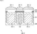
(単位画素の第1の構成)
図6は、CMOSイメージセンサ10が裏面型のイメージセンサである場合の単位画素100の断面図である。図6に示した単位画素100は、第1の構成であることを示すために、以下、単位画素100−1と記述する。
(First configuration of unit pixel)
FIG. 6 is a cross-sectional view of the
単位画素100−1は、図中上側から、オンチップレンズ201、カラーフィルタ202、遮光膜203、およびシリコン基板204が積層され、シリコン基板204には、第1光電変換部101と第2光電変換部103が形成されている。
The on-chip lens 201, the
なお、図示はしていないが、例えば、オンチップレンズ201の上側には、カバーガラスなどが積層され、シリコン基板204の下側には、配線層や支持基板が積層されている。以下の説明において必要な部分を適宜図示し、説明を加え、その他の部分については、適宜図示や説明を省略する。
Although not shown, for example, a cover glass or the like is laminated on the upper side of the on-chip lens 201, and a wiring layer or a support substrate is laminated on the lower side of the
図6では、第1光電変換部101−1、第1光電変換部101−2、および第2光電変換部103を図示している。また、これら3箇所の光電変換部上に、それぞれオンチップレンズ201−1乃至201−3が形成されている。
In FIG. 6, the first photoelectric conversion unit 101-1, the first photoelectric conversion unit 101-2, and the second
遮光膜203は、第2光電変換部103上にのみ形成されている。遮光膜203は、光を吸収、反射する機能を有する膜である。遮光膜203は、金属膜で形成され、光を反射する膜として形成されていても良いし、光の一部を吸収し、一部を透過する膜として形成されていても良いし、光を吸収する光吸収膜として形成されていても良い。
The light-shielding
遮光膜203は、例えば、アモルファスシリコン膜、ポリシリコン膜、ゲルマニウム(Ge)膜、窒化ガリウム(GaN)膜、テルル化カドミウム(CdTe)膜、ヒ化ガリウム(GaAs)膜、リン化インジウム(InP)膜、CuInSe2膜、Cu2S膜、CIGS膜、非導体構造のカーボン膜、黒色レジスト膜、有機光電変換膜などとされる。
The light-shielding
なお、以下に説明する第2乃至第16の構成においても、遮光膜が第2光電変換部103上に設けられている形態を示すが、それらの形態においても、遮光膜は、上記した材料で形成されるようにすることができる。なお、上記した遮光膜の材料は、一例であり、限定を示すものではない。
In addition, also in the 2nd to 16th configurations described below, the mode in which the light-shielding film is provided on the second
このように、低感度の第2光電変換部103上に遮光膜203を形成することで、オンチップレンズ201−3を透過してきた光が、遮光膜203に吸収され、第2光電変換部103に入射される光量が減少する。このため、第2光電変換部103の感度が、さらに低下することになるため、低感度の光電変化部としての性能は向上し、ダイナミックレンジを拡大することができる。
By forming the light-shielding
(単位画素の第2の構成)
次に、単位画素100の第2の構成について説明する。図7は、図6に示した単位画素100−1と同じく、CMOSイメージセンサ10が裏面型のイメージセンサである場合の単位画素100−2の断面図である。
(Second configuration of unit pixel)
Next, the second configuration of the
図7に示した単位画素100−2と、図6に示した単位画素100−1を比較するに、単位画素100−2は、単位画素100−1から第2光電変換部103上に形成されているオンチップレンズ201−3を削除した構成となされている点が異なり、他の部分は同一である。単位画素100−1と同様の構成を有する部分には、同様の符号を付し、その説明を省略する。以下、他の部分も同様に、適宜同様の部分に関しては説明を省略する。
Comparing the unit pixel 100-2 shown in FIG. 7 with the unit pixel 100-1 shown in FIG. 6, the unit pixel 100-2 is formed on the second
第2光電変換部103上にオンチップレンズ201−3を形成しない構成とすることで、第2光電変換部103に光が集光されない状態で入射される構成となり、第2光電変換部103に入射される光量が減少する。このため、第2光電変換部103の感度が、さらに低下し、低感度の光電変化部のダイナミックレンジを拡大させることが可能となる。
By not forming the on-chip lens 201-3 on the second
(単位画素の第3の構成)
次に、単位画素100の第3の構成について説明する。図8は、図6に示した単位画素100−1と同じく、CMOSイメージセンサ10が裏面型のイメージセンサである場合の単位画素100−3の断面図である。
(Third configuration of unit pixel)
Next, a third configuration of the
図8に示した単位画素100−3と、図6に示した単位画素100−1を比較するに、単位画素100−3は、単位画素100−1に遮光壁231を追加した構成となされている点が異なり、他の部分は同一である。
Comparing the unit pixel 100-3 shown in FIG. 8 with the unit pixel 100-1 shown in FIG. 6, the unit pixel 100-3 has a configuration in which a light-shielding
遮光壁231は、画素間に設けられており、図8に示した単位画素100−3においては、第1光電変換部101−1と第2光電変換部103の間、第1光電変換部101−2と第2光電変換部103の間にそれぞれ設けられている。このように、遮光壁231は、画素分離領域に設けられている。また遮光壁231は、受光面側から形成された絶縁膜で形成された溝で囲まれるように形成することができる。
The light-shielding
また遮光壁231は、トレンチを形成し、そのトレンチ内に、負の固定電荷膜と酸化膜を組み合わせて形成されるようにしても良いし、負の固定電荷膜、酸化膜、および金属を組み合わせて形成されるようにしても良い。
Further, the light-shielding
遮光壁231は、隣接する光電変換部への光の漏れ込みを防ぐために設けられている。遮光壁231を設けることで、混色などが発生することを低減させることが可能となる。
The light-shielding
このような構成とした場合においても、低感度の第2光電変換部103上に遮光膜203を形成することで、オンチップレンズ201−3を透過してきた光が、遮光膜203に吸収され、第2光電変換部103に入射される光量が減少する。このため、第2光電変換部103の感度が、さらに低下し、ダイナミックレンジを拡大させることが可能となる。また遮光壁231を設けることで、混色などの発生を低減させることが可能となる。
Even in such a configuration, by forming the light-shielding
(単位画素の第4の構成)
次に、単位画素100の第4の構成について説明する。図9は、図7に示した単位画素100−2と同じく、CMOSイメージセンサ10が裏面型のイメージセンサである場合の単位画素100−4の断面図である。
(Fourth configuration of unit pixel)
Next, a fourth configuration of the
図9に示した単位画素100−4と、図7に示した単位画素100−2を比較するに、単位画素100−4は、単位画素100−2に遮光壁231を追加した構成となされている点が異なり、他の部分、例えば、第2光電変換部103上のオンチップレンズ201−3が形成されていてない点などは同一である。また、遮光壁231を追加した構成は、図8に示した単位画素100−3と同様の構成である。
Comparing the unit pixel 100-4 shown in FIG. 9 with the unit pixel 100-2 shown in FIG. 7, the unit pixel 100-4 has a configuration in which a light-shielding
このような構成とした場合においても、低感度の第2光電変換部103上に遮光膜203を形成することで、遮光膜203に入射された光が吸収され、第2光電変換部103に入射される光量が減少し、さらにオンチップレンズが形成されていないために、さらに第2光電変換部103に入射される光量が減少するため、第2光電変換部103の感度が、さらに低下する構成となる。よって、低感度の光電変化部のダイナミックレンジを拡大させることが可能となる。また遮光壁231を設けることで、混色などの発生を低減させることが可能となる。
Even in such a configuration, by forming the light-shielding
(単位画素の第5の構成)
次に、単位画素100の第5の構成について説明する。図10は、図6に示した単位画素100−1と同じく、CMOSイメージセンサ10が裏面型のイメージセンサである場合の単位画素100−5の断面図である。
(Fifth configuration of unit pixel)
Next, a fifth configuration of the
図10に示した単位画素100−5と、図6に示した単位画素100−1を比較するに、単位画素100−5の遮光膜251は、単位画素100−1の遮光膜203と異なる形状をしている点が異なり、他の部分は同一である。単位画素100−5の遮光膜251は、スリットがある形状に形成されている。スリットに該当する部分には、遮光膜251が形成されていないようにしても良いし、スリットではない部分の遮光膜251よりも薄く形成されているようにしても良い。
Comparing the unit pixel 100-5 shown in FIG. 10 with the unit pixel 100-1 shown in FIG. 6, the light-shielding
遮光膜251をスリット形状とすることで、第2光電変換部103を偏光画素として用いることができる。
By forming the light-shielding
例えば、第2光電変換部103が車載され、道路表面を含む画像を撮像する場合、道路表面から反射された光は、道路の表面に平行な偏光となる。このような偏光を除去した撮影を行う場合には、道路表面と平行となる方向に遮光膜251のスリットを形成することで、道路表面で反射された光を選択的に沮止し、他の被写体からの光を受光することができる。
For example, when the second
このように、遮光膜251の形状をスリット形状とすることで、第2光電変換部103への光の量を少なくさせるだけでなく、不要な光を除去することも可能な構成とすることができる。
In this way, by forming the light-shielding
このように、遮光膜251を偏光子としても用いるようにした場合、遮光膜251の材料として、上記した材料の他に、金属を用いることも可能である。なお偏光子に遮光膜を使用することで、偏光子を金属で形成した場合より、効率よく直接、間接光を減光できる構成とすることができる。
As described above, when the light-shielding
このような構成とした場合においても、低感度の第2光電変換部103上に遮光膜251を形成することで、第2光電変換部103に入射される光量が減少し、低感度化によるダイナミックレンジの拡大を実現することができる。また、遮光膜251をスリット形状とすることで、遮光膜251を偏光子として用いることができ、反射光などの不要な光の影響を除去することができる。
Even in such a configuration, by forming the light-shielding
(単位画素の第6の構成)
次に、単位画素100の第6の構成について説明する。図11は、図7に示した単位画素100−2と同じく、CMOSイメージセンサ10が裏面型のイメージセンサである場合の単位画素100−6の断面図である。
(Sixth configuration of unit pixel)
Next, the sixth configuration of the
図11に示した単位画素100−6と、図7に示した単位画素100−2を比較するに、単位画素100−6の遮光膜251は、単位画素100−2の遮光膜203と異なる形状をしている点が異なり、他の部分、例えば、第2光電変換部103上にオンチップレンズ201−3が形成されていない点などは同一である。単位画素100−6の遮光膜251は、図10に示した単位画素100−5と同じく、スリット形状に形成されている。
Comparing the unit pixel 100-6 shown in FIG. 11 with the unit pixel 100-2 shown in FIG. 7, the light-shielding
遮光膜251をスリット形状とすることで、単位画素100−5(図10)と同じく、第2光電変換部103への光の量を少なくさせるだけでなく、不要な光を除去することも可能な構成とすることができる。
By forming the light-shielding
このような構成とした場合においても、低感度の第2光電変換部103上に遮光膜251を形成することで、第2光電変換部103に入射される光量が減少し、低感度化によるダイナミックレンジの拡大を実現することができる。また第2光電変換部103上にオンチップレンズを形成しないことで、第2光電変換部103に入射される光量がより減少し、低感度化によるダイナミックレンジの拡大を実現することができる。また、遮光膜251をスリット形状とすることで、遮光膜251を偏光子として用いることができ、反射光などの不要な光の影響を除去することができる。
Even in such a configuration, by forming the light-shielding
(単位画素の第7の構成)
次に、単位画素100の第7の構成について説明する。図12は、図8に示した単位画素100−3と同じく、CMOSイメージセンサ10が裏面型のイメージセンサである場合の単位画素100−7の断面図である。
(7th configuration of unit pixel)
Next, a seventh configuration of the
図12に示した単位画素100−7と、図8に示した単位画素100−3を比較するに、単位画素100−7は、遮光膜251がスリット形状に形成されている点が異なり、他の部分、例えば、画素間に遮光膜231が設けられている点などは同一である。
Comparing the unit pixel 100-7 shown in FIG. 12 with the unit pixel 100-3 shown in FIG. 8, the unit pixel 100-7 is different in that the light-shielding
このような構成とした場合においても、低感度の第2光電変換部103上に遮光膜251を形成することで、第2光電変換部103に入射される光量が減少し、低感度化によるダイナミックレンジの拡大を実現することができる。また、遮光膜251をスリット形状とすることで、遮光膜251を偏光子として用いることができ、反射光などの不要な光の影響を除去することができる。また遮光壁231を設けることで、混色などの発生を低減させることが可能となる。
Even in such a configuration, by forming the light-shielding
(単位画素の第8の構成)
次に、単位画素100の第8の構成について説明する。図13は、図9に示した単位画素100−4と同じく、CMOSイメージセンサ10が裏面型のイメージセンサである場合の単位画素100−8の断面図である。
(8th configuration of unit pixel)
Next, the eighth configuration of the
図13に示した単位画素100−8と、図9に示した単位画素100−4を比較するに、単位画素100−8は、遮光膜251がスリット形状に形成されている点が異なり、他の部分、例えば、単画素間に遮光膜231が設けられ、第2光電変換部103上にオンチップレンズが形成されていない点などは同一である。
Comparing the unit pixel 100-8 shown in FIG. 13 with the unit pixel 100-4 shown in FIG. 9, the unit pixel 100-8 is different in that the light-shielding
このような構成とした場合においても、低感度の第2光電変換部103上に遮光膜251を形成することで、第2光電変換部103に入射される光量が減少し、低感度化によるダイナミックレンジの拡大を実現することができる。また第2光電変換部103上にオンチップレンズを形成しないことで、第2光電変換部103に入射される光量がより減少し、低感度化によるダイナミックレンジの拡大を実現することができる。
Even in such a configuration, by forming the light-shielding
また、遮光膜251をスリット形状とすることで、遮光膜251を偏光子として用いることができ、反射光などの不要な光の影響を除去することができる。また遮光壁231を設けることで、混色などの発生を低減させることが可能となる。
Further, by forming the light-shielding
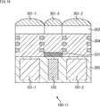
(単位画素の第9の構成)
図14は、CMOSイメージセンサ10が表面型のイメージセンサである場合の単位画素100−9の断面図である。
(Ninth configuration of unit pixel)
FIG. 14 is a cross-sectional view of unit pixels 100-9 when the CMOS image sensor 10 is a surface type image sensor.
図14に示した単位画素100−9は、図中上側から、オンチップレンズ301、カラーフィルタ302、遮光膜303、配線層304、およびシリコン基板305が積層され、シリコン基板305には、第1光電変換部101と第2光電変換部103が形成されている。
In the unit pixels 100-9 shown in FIG. 14, the on-chip lens 301, the
なお、図示はしていないが、例えば、オンチップレンズ201の上側には、カバーガラスなどが積層されている。以下の説明において必要な部分を適宜図示し、説明を加え、その他の部分については、適宜図示や説明を省略する。 Although not shown, for example, a cover glass or the like is laminated on the upper side of the on-chip lens 201. In the following description, necessary parts will be illustrated and described as appropriate, and other parts will not be illustrated or described as appropriate.
図14では、第1光電変換部101−1、第1光電変換部101−2、および第2光電変換部103を図示している。また、これら3箇所の光電変換部上に、それぞれオンチップレンズ301−1乃至301−3が形成されている。
In FIG. 14, the first photoelectric conversion unit 101-1, the first photoelectric conversion unit 101-2, and the second
遮光膜303は、第2光電変換部103上にのみ形成されている。遮光膜303は、例えば、アモルファスシリコン膜、ポリシリコン膜、Ge膜、GaN膜、CdTe膜、GaAs膜、InP膜、CuInSe2膜、Cu2S、CIGS膜、非導体構造のカーボン膜、黒色レジスト膜、有機光電変換膜で形成される。また、後述するように、遮光膜303が、スリット形状で形成される場合、金属で形成されるようにすることも可能である。なお、上記した遮光膜の材料は、一例であり、限定を示すものではない。
The light-shielding
このように、表面型のイメージセンサにおいても、低感度の第2光電変換部103上に遮光膜303を形成することで、オンチップレンズ301−3を透過してきた光が、遮光膜303に吸収され、第2光電変換部103に入射される光量が減少する。このため、第2光電変換部103の感度が、さらに低下することになるため、ダイナミックレンジは拡大することになる。
As described above, even in the surface type image sensor, by forming the light-shielding
(単位画素の第10の構成)
次に、単位画素100の第10の構成について説明する。図15は、図14に示した単位画素100−9と同じく、CMOSイメージセンサ10が表面型のイメージセンサである場合の単位画素100−10の断面図である。
(10th configuration of unit pixel)
Next, the tenth configuration of the
図15に示した単位画素100−10と、図14に示した単位画素100−9を比較するに、単位画素100−10は、単位画素100−9から第2光電変換部103上に形成されているオンチップレンズ301−3を削除した構成となされている点が異なり、他の部分は同一である。
Comparing the unit pixel 100-10 shown in FIG. 15 with the unit pixel 100-9 shown in FIG. 14, the unit pixel 100-10 is formed on the second
第2光電変換部103上にオンチップレンズ301−3を形成しない構成とすることで、第2光電変換部103に光が集光されない状態で入射される構成となり、第2光電変換部103に入射される光量が減少する。このため、第2光電変換部103の低感度化によるダイナミックレンジを拡大させることが可能となる。
By not forming the on-chip lens 301-3 on the second
(単位画素の第11の構成)
次に、単位画素100の第11の構成について説明する。図16は、図14に示した単位画素100−9と同じく、CMOSイメージセンサ10が表面型のイメージセンサである場合の単位画素100−11の断面図である。
(11th configuration of unit pixel)
Next, the eleventh configuration of the
図16に示した単位画素100−11と、図14に示した単位画素100−9を比較するに、単位画素100−9の遮光膜303は、配線層304の図中上側(オンチップ301側)に形成されているのに対して、単位画素100−11の遮光膜は、配線層304の図中下側(シリコン基板305側)に形成されている点が異なり、他の部分は同一である。
Comparing the unit pixels 100-11 shown in FIG. 16 and the unit pixels 100-9 shown in FIG. 14, the light-shielding
再度図14を参照するに、単位画素100−9の遮光膜303は、配線層304の上側であり、カラーフィルタ302の層内に形成されている。これに対して、図15に示した単位画素100−11の遮光膜331は、配線層304の下側であり、シリコン基板305の上側の配線層304内に形成されている。このように、遮光膜が形成される位置は、配線層304の上側でも良いし、下側でも良い。
With reference to FIG. 14 again, the light-shielding
このように、表面型のイメージセンサにおいても、低感度の第2光電変換部103上に遮光膜303を形成することで、オンチップレンズ301−3を透過してきた光が、遮光膜303に吸収され、第2光電変換部103に入射される光量が減少する。このため、第2光電変換部103の感度が、さらに低下し、ダイナミックレンジを拡大させることが可能となる。
As described above, even in the surface type image sensor, by forming the light-shielding
(単位画素の第12の構成)
次に、単位画素100の第12の構成について説明する。図17は、図16に示した単位画素100−11と同じく、CMOSイメージセンサ10が表面型のイメージセンサである場合の単位画素100−12の断面図である。
(12th configuration of unit pixel)
Next, the twelfth configuration of the
図17に示した単位画素100−12と、図16に示した単位画素100−11を比較するに、単位画素100−12は、単位画素100−11から第2光電変換部103上に形成されているオンチップレンズ301−3を削除した構成となされている点が異なり、他の部分は同一である。
Comparing the unit pixel 100-12 shown in FIG. 17 with the unit pixel 100-11 shown in FIG. 16, the unit pixel 100-12 is formed on the second
第2光電変換部103上にオンチップレンズ301−3を形成しない構成とすることで、第2光電変換部103に光が集光されない状態で入射される構成となり、第2光電変換部103に入射される光量が減少する。このため、第2光電変換部103の低下化のダイナミックレンジを拡大させることが可能となる。
By not forming the on-chip lens 301-3 on the second
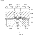
(単位画素の第13の構成)
次に、単位画素100の第13の構成について説明する。図18は、図14に示した単位画素100−9と同じく、CMOSイメージセンサ10が表面型のイメージセンサである場合の単位画素100−13の断面図である。
(13th configuration of unit pixel)
Next, the thirteenth configuration of the
図18に示した単位画素100−13と、図14に示した単位画素100−9を比較するに、単位画素100−13の遮光膜351は、単位画素100−9の遮光膜303と異なる形状をしている点が異なり、他の部分は同一である。単位画素100−13の遮光膜351は、スリット形状に形成され、カラーフィルタ302の層内に形成されている。
Comparing the unit pixel 100-13 shown in FIG. 18 and the unit pixel 100-9 shown in FIG. 14, the light-shielding
遮光膜351をスリット形状とすることで、遮光膜351を偏光子として用いることができ、第2光電変換部103を偏光画素として用いることができる。
By forming the light-shielding
このような構成とした場合においても、低感度の第2光電変換部103上に遮光膜351を形成することで、第2光電変換部103に入射される光量が減少し、低感度化によるダイナミックレンジの拡大を実現することができる。また、遮光膜351をスリット形状とすることで、遮光膜351を偏光子として用いることができ、反射光などの不要な光の影響を除去することができる。
Even in such a configuration, by forming the light-shielding
(単位画素の第14の構成)
次に、単位画素100の第14の構成について説明する。図19は、図18に示した単位画素100−13と同じく、CMOSイメージセンサ10が表面型のイメージセンサである場合の単位画素100−14の断面図である。
(14th configuration of unit pixel)
Next, the 14th configuration of the
図19に示した単位画素100−14と、図18に示した単位画素100−13を比較するに、単位画素100−14は、単位画素100−13から第2光電変換部103上に形成されているオンチップレンズ301−3を削除した構成となされている点が異なり、他の部分は同一である。単位画素100−14の遮光膜351は、スリット形状で形成され、カラーフィルタ302の層内に形成されている。
Comparing the unit pixel 100-14 shown in FIG. 19 with the unit pixel 100-13 shown in FIG. 18, the unit pixel 100-14 is formed on the second
第2光電変換部103上にオンチップレンズ301−3を形成しない構成とすることで、第2光電変換部103に光が集光されない状態で入射される構成となり、第2光電変換部103に入射される光量が減少する。このため、第2光電変換部103の感度が、さらに低下することになるため、ダイナミックレンジを拡大させることが可能となる。また、遮光膜351をスリット形状とすることで、遮光膜351を偏光子として用いることができ、反射光などの不要な光の影響を除去することができる。
By not forming the on-chip lens 301-3 on the second
(単位画素の第15の構成)
次に、単位画素100の第15の構成について説明する。図20は、図18に示した単位画素100−13と同じく、CMOSイメージセンサ10が表面型のイメージセンサである場合の単位画素100−15の断面図である。
(15th configuration of unit pixel)
Next, the fifteenth configuration of the
図20に示した単位画素100−15と、図18に示した単位画素100−13を比較するに、単位画素100−13の遮光膜351は、配線層304の図中上側に形成されているのに対して、単位画素100−15の遮光膜381は、配線層304の図中下側に形成されている点が異なり、他の部分は同一である。すなわち、単位画素100−15の遮光膜381は、配線層304の下側にスリット形状で形成されている。
Comparing the unit pixel 100-15 shown in FIG. 20 with the unit pixel 100-13 shown in FIG. 18, the light-shielding
このような構成の表面型のイメージセンサにおいても、低感度の第2光電変換部103上に遮光膜381を形成することで、オンチップレンズ301−3を透過してきた光が、遮光膜381に吸収され、第2光電変換部103に入射される光量が減少する。このため、第2光電変換部103の低感度化によるダイナミックレンジを拡大させることが可能となる。また、遮光膜381をスリット形状とすることで、遮光膜351を偏光子として用いることができ、反射光などの不要な光の影響を除去することが可能となる。
Even in a surface-type image sensor having such a configuration, by forming a light-shielding
(単位画素の第16の構成)
次に、単位画素100の第16の構成について説明する。図21は、図20に示した単位画素100−15と同じく、CMOSイメージセンサ10が表面型のイメージセンサである場合の単位画素100−16の断面図である。
(16th configuration of unit pixel)
Next, the 16th configuration of the
図21に示した単位画素100−16と、図20に示した単位画素100−15を比較するに、単位画素100−16は、単位画素100−15から第2光電変換部103上に形成されているオンチップレンズ301−3を削除した構成となされている点が異なり、他の部分は同一である。すなわち、端画素100−16の遮光膜381は、配線層304の下側にスリット形状で形成されている。
Comparing the unit pixel 100-16 shown in FIG. 21 with the unit pixel 100-15 shown in FIG. 20, the unit pixel 100-16 is formed on the second
第2光電変換部103上にオンチップレンズ301−3を形成しない構成とすることで、第2光電変換部103に光が集光されない状態で入射される構成となり、第2光電変換部103に入射される光量が減少する。このため、第2光電変換部103の低感度化によるダイナミックレンジを拡大させることが可能となる。また、遮光膜381をスリット形状とすることで、遮光膜381を偏光子として用いることができ、反射光などの不要な光の影響を除去することが可能となる。
By not forming the on-chip lens 301-3 on the second
第1乃至第16の構成として示したように、低感度の第2光電変換部103上に、光を吸収する機能を有する膜を形成し、第2光電変換部103に入射される光の量を減少させることで、低感度化によるダイナミックレンジを拡大させることが可能となる。
As shown as the first to 16th configurations, a film having a function of absorbing light is formed on the low-sensitivity second
また、遮光膜をスリット形状とすることで、偏光子として用いることができ、偏光子を設けることで反射光の影響(不要な光の影響)を除去し、低感度化によるダイナミックレンジを拡大することを同時に実現することができる。 In addition, the light-shielding film has a slit shape, so that it can be used as a polarizer. By providing a polarizing film, the influence of reflected light (the influence of unnecessary light) is removed, and the dynamic range is expanded by lowering the sensitivity. Can be achieved at the same time.
また偏光子に遮光膜を使用することで、偏光子を金属で形成した場合より、効率よく直接、間接光を減光できる構成とすることができる。 Further, by using a light-shielding film for the polarizer, it is possible to form a configuration in which indirect light can be dimmed more efficiently than when the polarizer is made of metal.
<第1、第2光電変換部の配置について>
第1光電変換部101と第2光電変換部103を含む単位画素100は、例えば、図22に示すように配置されている。図22においては、単位画素500とし、単位画素500は、上記した単位画素100−1乃至100−18のいずれかであるとして説明を続ける。
<About the arrangement of the first and second photoelectric conversion units>
The
図22では、4×4の16個の単位画素500−1乃至500−16が配置されている例を示した。各単位画素500は、第1光電変換部101と第2光電変換部103を含む。例えば、単位画素500−1は、第1光電変換部101−1と第2光電変換部103−1を含む。
FIG. 22 shows an example in which 16 4 × 4 unit pixels 500-1 to 500-16 are arranged. Each unit pixel 500 includes a first
第1光電変換部101と第2光電変換部103は、受光面の大きさにより異なる感度となるように構成されている。すなわち、図22に示したように、第1光電変換部101の受光面は、第2光電変換部103の受光面よりも大きくなるように構成されている。
The first
図22に示した例では、例えば、第1光電変換部101−1の右斜め下に第2光電変換部103−1が配置されている。図示はしていないが、第1光電変換部101−1の右横に第2光電変換部103−1が配置されるようにしても良い。また、他の配置関係でも良い。 In the example shown in FIG. 22, for example, the second photoelectric conversion unit 103-1 is arranged diagonally to the lower right of the first photoelectric conversion unit 101-1. Although not shown, the second photoelectric conversion unit 103-1 may be arranged on the right side of the first photoelectric conversion unit 101-1. Moreover, other arrangement relations may be used.
単位画素500内で、第1光電変換部101と第2光電変換部103が配置されていない部分には、信号処理回路などを配置するようにしても良い。すなわち、異なる受光面積の第1光電変換部101と第2光電変換部103が、単位画素500内に配置されることで、余剰な領域が発生するが、その余剰な領域に信号処理回路などを配置することで、領域を有効利用するようにしても良い。
A signal processing circuit or the like may be arranged in a portion of the unit pixel 500 where the first
単位画素500上に配置されるカラーフィルタ202(302)の色は、例えば、ベイヤ−配列とすることができる。図23Aに示すように、単位画素500−1を赤色(R)、単位画素500−2を緑色(G)、単位画素500−5を緑色(G)、単位画素500−6を青色(B)とする色配置にすることができる。 The color of the color filter 202 (302) arranged on the unit pixel 500 can be, for example, a Bayer array. As shown in FIG. 23A, the unit pixel 500-1 is red (R), the unit pixel 500-2 is green (G), the unit pixel 500-5 is green (G), and the unit pixel 500-6 is blue (B). The color arrangement can be set to.
このような色配置とされた場合、図22と図23Aを再度参照するに、例えば、単位画素500−1には、第1光電変換部101−1と第2光電変換部103−1が配置され、カラーフィルタ202(302、以下、202を例に挙げて説明する)の色は、赤色(R)である。このように、同一の単位画素500内に配置されている第1光電変換部101と第2光電変換部103は、同一のカラーフィルタ202の色とされている。
In the case of such a color arrangement, referring to FIGS. 22 and 23A again, for example, the first photoelectric conversion unit 101-1 and the second photoelectric conversion unit 103-1 are arranged in the unit pixel 500-1. The color of the color filter 202 (302, hereinafter, 202 will be described as an example) is red (R). As described above, the first
図23Bに示すように、4画素を同色としたベイヤ−配列としても良い。図23Bにおいては、単位画素500−1、単位画素500−2、単位画素500−5、単位画素500−6が赤色(R)、単位画素500−3、単位画素500−4、単位画素500−7、単位画素500−8が緑色(G)、単位画素500−9、単位画素500−10、単位画素500−13、単位画素500−14が緑色(G)、単位画素500−11、単位画素500−12、単位画素500−15、単位画素500−16が緑色(G)とされている。 As shown in FIG. 23B, a Bayer array in which four pixels have the same color may be used. In FIG. 23B, the unit pixel 500-1, the unit pixel 500-2, the unit pixel 500-5, and the unit pixel 500-6 are red (R), the unit pixel 500-3, the unit pixel 500-4, and the unit pixel 500-. 7. Unit pixel 500-8 is green (G), unit pixel 500-9, unit pixel 500-10, unit pixel 500-13, unit pixel 500-14 is green (G), unit pixel 500-11, unit pixel 500-12, unit pixel 500-15, and unit pixel 500-16 are green (G).
ここでは、色配置として、ベイヤ−配列を例に挙げて説明したが、他の色配置であっても本技術を適用できる。 Here, the Bayer-arrangement has been described as an example of the color arrangement, but the present technology can be applied to other color arrangements.
第2光電変換部103上には、上記したように、遮光膜が形成されている。遮光膜としては、図6などに示したスリット形状ではない遮光膜203(以下、ベタ形状の遮光膜203と記述する)と、図10などに示したスリット形状の遮光膜251がある。
As described above, a light-shielding film is formed on the second
なおここでは、ベタ形状の遮光膜として、遮光膜203(図6)を例に挙げて説明するが、遮光膜303(図14)、遮光膜331(図16)に対しても、以下の説明は適用される。また、スリット形状の遮光膜として、遮光膜251(図10)を例に挙げて説明するが、遮光膜351(図18)、遮光膜381(図20)に対しても、以下の説明は適用される。 Here, the light-shielding film 203 (FIG. 6) will be described as an example of the solid-shaped light-shielding film, but the following description will also be given to the light-shielding film 303 (FIG. 14) and the light-shielding film 331 (FIG. 16). Applies. Further, as the slit-shaped light-shielding film, the light-shielding film 251 (FIG. 10) will be described as an example, but the following description is also applied to the light-shielding film 351 (FIG. 18) and the light-shielding film 381 (FIG. 20). Will be done.
ベタ形状の遮光膜203が形成されている場合、例えば、図24Aに示したように遮光膜203は形成される。図24Aでは、図22に示した4×4の16個の単位画素500−1乃至500−16のうちの左上側に配置されている4画素だけ図示してあるが、他の画素も同様に遮光膜203が形成されている。
When the solid light-shielding
図24Aに示すように、単位画素500内の第2光電変換部103上には、ベタ形状の遮光膜203が形成されている。例えば、図24Aに示した単位画素500−1内の右下に、第2光電変換部103が形成され、その第2光電変換部103−1が形成されている領域に、遮光膜203−1が形成される。
As shown in FIG. 24A, a solid light-shielding
なお、図24Aに示したように、遮光膜203は、画素外周領域でウェル(WELL)に接続されているように形成されるようにすることができる。
As shown in FIG. 24A, the light-shielding
スリット形状の遮光膜251が形成されている場合、例えば、図24Bに示したように遮光膜251が形成される。図24Bに示すように、単位画素500内の第2光電変換部103上には、スリット形状の遮光膜251が形成されている。
When the slit-shaped light-shielding
図24Bに示したスリットの方向は、図中横方向であり、4画素とも同方向のスリットとされている。このように、第2光電変換部103上に設けられる遮光膜251のスリットは、全て同一の方向を有しているように形成することができる。
The direction of the slit shown in FIG. 24B is the horizontal direction in the drawing, and all four pixels are slits in the same direction. In this way, the slits of the light-shielding
遮光膜251のスリットの方向を、画素毎に変えるようにしても良い。図24Cは、単位画素500内の第2光電変換部103上に、スリット形状の遮光膜251が形成されている場合であり、画素毎に異なる方向のスリットが形成されている場合の遮光膜251を示している。
The direction of the slit of the light-shielding
図24Cに示した単位画素500−1内の第2光電変換部103−1上に形成されている遮光膜251−1のスリットは、図中、横方向に形成されている。単位画素500−2内の第2光電変換部103−2上に形成されている遮光膜251−2のスリットは、図中、左斜め下方向に形成されている。 The slit of the light-shielding film 251-1 formed on the second photoelectric conversion unit 103-1 in the unit pixel 500-1 shown in FIG. 24C is formed in the lateral direction in the drawing. The slit of the light-shielding film 251-2 formed on the second photoelectric conversion unit 103-2 in the unit pixel 500-2 is formed in the diagonally downward left direction in the drawing.
単位画素500−5内の第2光電変換部103−5上に形成されている遮光膜251−5のスリットは、図中、右斜め下方向に形成されている。単位画素500−6内の第2光電変換部103−6上に形成されている遮光膜251−6のスリットは、図中、縦方向に形成されている。 The slits of the light-shielding film 251-5 formed on the second photoelectric conversion unit 103-5 in the unit pixel 500-5 are formed in the diagonally downward right direction in the drawing. The slits of the light-shielding film 251-6 formed on the second photoelectric conversion unit 103-6 in the unit pixel 500-6 are formed in the vertical direction in the drawing.
図24Cに示した例では、4方向のスリットが形成されている場合を示している。図示していない他の画素も、2×2の4画素内で、それぞれの画素上の遮光膜251は、異なる4方向のスリット形状で形成されている。なおここでは、4方向を例に挙げて説明したが、さらに他の方向が追加されたり、2方向または3方向など、遮光膜251のスリットの方向は、4方向に限定されるわけではない。
In the example shown in FIG. 24C, a case where slits in four directions are formed is shown. Other pixels (not shown) are also within 2 × 2 4 pixels, and the light-shielding
このように、画素毎にスリットの方向を変える、換言すれば、隣接する第2光電変換部103上に形成された遮光膜251のスリット方向が異なるようにすることで、異なる方向からの偏光を沮止することが可能となる。
In this way, the direction of the slit is changed for each pixel, in other words, by making the slit direction of the light-shielding
また、このように、画素毎にスリットの方向が変わるように形成した場合、例えば、図24Cに示した4画素単位で、それぞれ異なる方向のスリットが形成される場合、単位とされる4画素は同一色としても良い。すなわち、図23Bに示したように、4画素が同一色とされたベイヤ−配列とされ、同一色とされている4画素内の画素同士は異なる方向のスリットとされている構成としても良い。 Further, when the slits are formed so as to change the direction of the slit for each pixel in this way, for example, when slits in different directions are formed in units of 4 pixels shown in FIG. 24C, the 4 pixels as a unit are It may be the same color. That is, as shown in FIG. 23B, a Bayer array in which the four pixels have the same color may be used, and the pixels in the four pixels having the same color may have slits in different directions.
<変形例>
以上の説明では、1画素内に感度が異なる2つの光電変換部を設ける例を示したが、1画素内に3つ以上の感度が異なる光電変換部を設けることも可能である。また感度の違いは、遮光膜の材料の違いや膜厚の違いなどで調整することも可能である。
<Modification example>
In the above description, an example in which two photoelectric conversion units having different sensitivities are provided in one pixel has been shown, but it is also possible to provide three or more photoelectric conversion units having different sensitivities in one pixel. The difference in sensitivity can also be adjusted by the difference in the material of the light-shielding film and the difference in the film thickness.
また、上記した実施の形態では、単位画素が行列状に配置されているCMOSイメージセンサに適用した場合を例に挙げて説明したが、本技術は、CMOSイメージセンサへの適用に限定されるものではない。すなわち、本技術は、単位画素が行列状に2次元配置されているX−Yアドレス方式の撮像装置全般に対して適用可能である。 Further, in the above-described embodiment, the case where the unit pixels are applied to the CMOS image sensor arranged in a matrix has been described as an example, but the present technology is limited to the application to the CMOS image sensor. is not. That is, this technique can be applied to all XY address type imaging devices in which unit pixels are two-dimensionally arranged in a matrix.
さらに、本技術は、可視光の入射光量の分布を検知して画像として撮像する撮像装置への適用に限らず、赤外線やX線、あるいは粒子等の入射量の分布を画像として撮像する撮像装置全般に対して適用可能である。 Furthermore, this technology is not limited to application to an imaging device that detects the distribution of the amount of incident light of visible light and captures it as an image, but is also an imaging device that captures the distribution of the amount of incident light such as infrared rays, X-rays, or particles as an image. Applicable to all.
なお、撮像装置はワンチップとして形成された形態であってもよいし、撮像部と、信号処理部または光学系とがまとめてパッケージングされた撮像機能を有するモジュール状の形態であってもよい。 The image pickup apparatus may be formed as a single chip, or may be a modular form having an image pickup function in which the image pickup unit and the signal processing unit or the optical system are packaged together. ..
<撮像装置の使用例>
図25は、上述の撮像装置の使用例を示す図である。
<Usage example of imaging device>
FIG. 25 is a diagram showing a usage example of the above-mentioned imaging device.
上述した撮像装置は、例えば、以下のように、可視光や、赤外光、紫外光、X線等の光をセンシングする様々なケースに使用することができる。 The above-mentioned imaging device can be used in various cases for sensing light such as visible light, infrared light, ultraviolet light, and X-ray, as described below.
・デジタルカメラや、カメラ機能付きの携帯機器等の、鑑賞の用に供される画像を撮影する装置
・自動停止等の安全運転や、運転者の状態の認識等のために、自動車の前方や後方、周囲、車内等を撮影する車載用センサ、走行車両や道路を監視する監視カメラ、車両間等の測距を行う測距センサ等の、交通の用に供される装置
・ユーザのジェスチャを撮影して、そのジェスチャに従った機器操作を行うために、TVや、冷蔵庫、エアーコンディショナ等の家電に供される装置
・内視鏡や、赤外光の受光による血管撮影を行う装置等の、医療やヘルスケアの用に供される装置
・防犯用途の監視カメラや、人物認証用途のカメラ等の、セキュリティの用に供される装置
・肌を撮影する肌測定器や、頭皮を撮影するマイクロスコープ等の、美容の用に供され装置
・スポーツ用途等向けのアクションカメラやウェアラブルカメラ等の、スポーツの用に供される装置
・畑や作物の状態を監視するためのカメラ等の、農業の用に供される装置
・ Devices that take images for viewing, such as digital cameras and portable devices with camera functions. ・ For safe driving such as automatic stop and recognition of the driver's condition, in front of the car Devices used for traffic, such as in-vehicle sensors that photograph the rear, surroundings, and interior of vehicles, surveillance cameras that monitor traveling vehicles and roads, and distance measurement sensors that measure distance between vehicles, etc. ・ User gestures Equipment used for home appliances such as TVs, refrigerators, and air conditioners in order to take pictures and operate the equipment according to the gestures ・ Endoscopes, devices that perform angiography by receiving infrared light, etc. Equipment used for medical and healthcare ・ Equipment used for security such as surveillance cameras for crime prevention and cameras for person authentication ・ Skin measuring instruments for taking pictures of the skin and taking pictures of the scalp Equipment used for beauty such as microscopes ・ Equipment used for sports such as action cameras and wearable cameras for sports applications ・ Camera for monitoring the condition of fields and crops, etc. Equipment used for agriculture
図26は、本技術を適用した電子機器の一例である撮像装置(カメラ装置)1001の構成例を示すブロック図である。 FIG. 26 is a block diagram showing a configuration example of an image pickup device (camera device) 1001 which is an example of an electronic device to which the present technology is applied.
図26に示すように、撮像装置1001は、レンズ群1011などを含む光学系、撮像素子1012、カメラ信号処理部であるDSP1013、フレームメモリ1014、表示装置1015、記録装置1016、操作系1017、及び、電源系1018等を有している。そして、DSP1013、フレームメモリ1014、表示装置1015、記録装置1016、操作系1017、及び、電源系1018がバスライン1019を介して相互に接続された構成となっている。
As shown in FIG. 26, the image pickup device 1001 includes an optical system including a
レンズ群1011は、被写体からの入射光(像光)を取り込んで撮像素子1012の撮像面上に結像する。撮像素子1012は、レンズ群1011によって撮像面上に結像された入射光の光量を画素単位で電気信号に変換して画素信号として出力する。
The
表示装置1015は、液晶表示装置や有機EL(electro luminescence)表示装置等のパネル型表示装置から成り、撮像素子1012で撮像された動画または静止画を表示する。記録装置1016は、撮像素子1012で撮像された動画または静止画を、メモリカードやビデオテープやDVD(Digital Versatile Disk)等の記録媒体に記録する。
The
操作系1017は、ユーザによる操作の下に、本撮像装置1001が持つ様々な機能について操作指令を発する。電源系1018は、DSP1013、フレームメモリ1014、表示装置1015、記録装置1016、及び、操作系1017の動作電源となる各種の電源を、これら供給対象に対して適宜供給する。
The
このような撮像装置1001は、ビデオカメラやデジタルスチルカメラ、更には、スマートフォン、携帯電話機等のモバイル機器向けカメラモジュールに適用される。そして、この撮像装置1001において、撮像素子1012として、上述した各実施形態に係る撮像装置を用いることができる。これにより、撮像装置1001の画質を向上させることができる。
Such an imaging device 1001 is applied to a video camera, a digital still camera, and a camera module for mobile devices such as smartphones and mobile phones. Then, in the image pickup device 1001, the image pickup device according to each of the above-described embodiments can be used as the
本明細書において、システムとは、複数の装置により構成される装置全体を表すものである。 As used herein, the term "system" refers to an entire device composed of a plurality of devices.
なお、本明細書に記載された効果はあくまで例示であって限定されるものでは無く、また他の効果があってもよい。 The effects described in the present specification are merely examples and are not limited, and other effects may be obtained.
なお、本技術の実施の形態は、上述した実施の形態に限定されるものではなく、本技術の要旨を逸脱しない範囲において種々の変更が可能である。 The embodiment of the present technology is not limited to the above-described embodiment, and various changes can be made without departing from the gist of the present technology.
なお、本技術は以下のような構成も取ることができる。
(1)
複数の単位画素が配置されている画素アレイ部の前記単位画素が、
第1の光電変換部と、
前記第1の光電変換部より感度が低い第2の光電変換部と
を備え、
前記第2の光電変換部の光が入射する側に、遮光膜が形成されている
撮像装置。
(2)
前記第2の光電変換部上には、入射される光を集光するためのレンズは形成されていない
前記(1)に記載の撮像装置。
(3)
隣接する光電変化部への光の漏れ込みを防ぐ遮光壁が、光電変換部間に備えられる
前記(1)または(2)に記載の撮像装置。
(4)
前記遮光膜は、スリット形状である
前記(1)乃至(3)のいずれかに記載の撮像装置。
(5)
隣接する第2の光電変換部上に形成されている前記遮光膜のスリットの方向は、異なる方向とされている
前記(4)に記載の撮像装置。
(6)
裏面型のイメージセンサである
前記(1)乃至(5)のいずれかに記載の撮像装置。
(7)
表面型のイメージセンサである
前記(1)乃至(5)のいずれかに記載の撮像装置。
(8)
前記遮光膜は、前記第2の光電変換部上に形成されている配線層の下側または上側に形成されている
前記(7)に記載の撮像装置。
(9)
前記遮光膜は、アモルファスシリコン膜、ポリシリコン膜、Ge膜、GaN膜、CdTe膜、GaAs膜、InP膜、CuInSe2膜、Cu2S、CIGS膜、非導体構造のカーボン膜、黒色レジスト膜、有機光電変換膜、または金属膜である
前記(1)乃至(8)のいずれかに記載の撮像装置。
The present technology can also have the following configurations.
(1)
The unit pixel of the pixel array unit in which a plurality of unit pixels are arranged is
The first photoelectric conversion unit and
It is provided with a second photoelectric conversion unit having a lower sensitivity than the first photoelectric conversion unit.
An imaging device in which a light-shielding film is formed on the side where the light of the second photoelectric conversion unit is incident.
(2)
The imaging device according to (1) above, wherein a lens for collecting incident light is not formed on the second photoelectric conversion unit.
(3)
The imaging device according to (1) or (2) above, wherein a light-shielding wall for preventing light from leaking to an adjacent photoelectric change portion is provided between the photoelectric conversion portions.
(4)
The imaging device according to any one of (1) to (3) above, wherein the light-shielding film has a slit shape.
(5)
The imaging device according to (4) above, wherein the slits of the light-shielding film formed on the adjacent second photoelectric conversion unit have different directions.
(6)
The imaging device according to any one of (1) to (5) above, which is a back-side type image sensor.
(7)
The imaging device according to any one of (1) to (5) above, which is a surface type image sensor.
(8)
The imaging device according to (7) above, wherein the light-shielding film is formed on the lower side or the upper side of the wiring layer formed on the second photoelectric conversion unit.
(9)
The light-shielding film is an amorphous silicon film, a polysilicon film, a Ge film, a GaN film, a CdTe film, a GaAs film, an InP film, a CuInSe2 film, a Cu2S, a CIGS film, a carbon film having a non-conductor structure, a black resist film, and an organic photoelectric conversion. The imaging apparatus according to any one of (1) to (8) above, which is a film or a metal film.
10 CMOSイメージセンサ, 11 画素アレイ部, 12 垂直駆動部, 13 カラム処理部, 14 水平駆動部, 15 システム制御部, 16 画素駆動線, 17 垂直信号線, 18 信号処理部, 19 データ格納部, 100 単位画素, 101 第1光電変換部, 102 第1の転送ゲート部, 103 第2光電変換部, 104 第2転送ゲート部, 105 第3転送ゲート部, 106 電荷蓄積部, 107 リセットゲート部, 108 FD部, 109 増幅トランジスタ, 110 選択トランジスタ, 151 第4転送ゲート部, 203,251,303,331,351,381 遮光膜 10 CMOS image sensor, 11 pixel array unit, 12 vertical drive unit, 13 column processing unit, 14 horizontal drive unit, 15 system control unit, 16 pixel drive line, 17 vertical signal line, 18 signal processing unit, 19 data storage unit, 100 unit pixels, 101 1st photoelectric conversion unit, 102 1st transfer gate unit, 103 2nd photoelectric conversion unit, 104 2nd transfer gate unit, 105 3rd transfer gate unit, 106 charge storage unit, 107 reset gate unit, 108 FD part, 109 amplification transistor, 110 selection transistor, 151 4th transfer gate part, 203,251,303,331,351,381 light-shielding film
Claims (8)
第1の光電変換部と、
前記第1の光電変換部の受光面よりも小さい受光面の第2の光電変換部と
を備え、
前記第2の光電変換部の光が入射する側にスリット形状の遮光膜が形成され、2×2の4画素のそれぞれの画素上の前記遮光膜は異なる4方向のスリット形状で形成されている
撮像装置。 The unit pixel of the pixel array unit in which a plurality of unit pixels are arranged is
The first photoelectric conversion unit and
A second photoelectric conversion unit having a light receiving surface smaller than the light receiving surface of the first photoelectric conversion unit is provided.
A slit-shaped light-shielding film is formed on the side where the light of the second photoelectric conversion unit is incident, and the light-shielding film on each of the 2 × 2 4 pixels is formed in a slit shape in different four directions. Imaging device.
請求項1に記載の撮像装置。 The imaging device according to claim 1, wherein a lens for collecting incident light is not formed on the second photoelectric conversion unit.
請求項1または2に記載の撮像装置。 The imaging device according to claim 1 or 2, wherein a light-shielding wall for preventing light from leaking into an adjacent photoelectric change unit is provided between the photoelectric conversion units.
請求項1乃至3のいずれかに記載の撮像装置。 The imaging device according to any one of claims 1 to 3 , wherein the four pixels in which the slit-shaped light-shielding film is arranged have the same color .
請求項1乃至4のいずれかに記載の撮像装置。 The imaging device according to any one of claims 1 to 4 , which is a back-side type image sensor.
請求項1乃至4のいずれかに記載の撮像装置。 The imaging device according to any one of claims 1 to 4 , which is a surface-type image sensor.
請求項6に記載の撮像装置。 The imaging device according to claim 6 , wherein the light-shielding film is formed on the lower side or the upper side of the wiring layer formed on the second photoelectric conversion unit.
請求項1乃至7のいずれかに記載の撮像装置。 The light-shielding film is an amorphous silicon film, a polysilicon film, a Ge film, a GaN film, a CdTe film, a GaAs film, an InP film, a CuInSe2 film, a Cu2S, a CIGS film, a carbon film having a non-conductor structure, a black resist film, and an organic photoelectric conversion. The imaging apparatus according to any one of claims 1 to 7 , which is a film or a metal film.
Priority Applications (9)
| Application Number | Priority Date | Filing Date | Title |
|---|---|---|---|
| JP2015209533A JP6754157B2 (en) | 2015-10-26 | 2015-10-26 | Imaging device |
| CN202211225689.9A CN115472639A (en) | 2015-10-26 | 2016-10-12 | Photodetector and electronic device |
| CN201680060810.3A CN108140661B (en) | 2015-10-26 | 2016-10-12 | Imaging device and electronic apparatus |
| PCT/JP2016/080220 WO2017073322A1 (en) | 2015-10-26 | 2016-10-12 | Image pick-up apparatus |
| EP16790735.1A EP3369113A1 (en) | 2015-10-26 | 2016-10-12 | Image pick-up apparatus |
| US15/768,378 US10741599B2 (en) | 2015-10-26 | 2016-10-12 | Image pick-up apparatus |
| KR1020187010717A KR20180075497A (en) | 2015-10-26 | 2016-10-12 | The image pickup device |
| US16/924,010 US11271026B2 (en) | 2015-10-26 | 2020-07-08 | Image pick-up apparatus |
| US17/574,033 US20220216249A1 (en) | 2015-10-26 | 2022-01-12 | Image pick-up apparatus |
Applications Claiming Priority (1)
| Application Number | Priority Date | Filing Date | Title |
|---|---|---|---|
| JP2015209533A JP6754157B2 (en) | 2015-10-26 | 2015-10-26 | Imaging device |
Related Child Applications (1)
| Application Number | Title | Priority Date | Filing Date |
|---|---|---|---|
| JP2020091641A Division JP2020141146A (en) | 2020-05-26 | 2020-05-26 | Imaging device |
Publications (3)
| Publication Number | Publication Date |
|---|---|
| JP2017084892A JP2017084892A (en) | 2017-05-18 |
| JP2017084892A5 JP2017084892A5 (en) | 2018-10-18 |
| JP6754157B2 true JP6754157B2 (en) | 2020-09-09 |
Family
ID=57227031
Family Applications (1)
| Application Number | Title | Priority Date | Filing Date |
|---|---|---|---|
| JP2015209533A Active JP6754157B2 (en) | 2015-10-26 | 2015-10-26 | Imaging device |
Country Status (6)
| Country | Link |
|---|---|
| US (3) | US10741599B2 (en) |
| EP (1) | EP3369113A1 (en) |
| JP (1) | JP6754157B2 (en) |
| KR (1) | KR20180075497A (en) |
| CN (2) | CN108140661B (en) |
| WO (1) | WO2017073322A1 (en) |
Cited By (1)
| Publication number | Priority date | Publication date | Assignee | Title |
|---|---|---|---|---|
| US11553151B2 (en) | 2018-09-28 | 2023-01-10 | Sony Semiconductor Solutions Corporation | Solid-state imaging device, method of controlling solid-state imaging device, and electronic device |
Families Citing this family (32)
| Publication number | Priority date | Publication date | Assignee | Title |
|---|---|---|---|---|
| JP6754157B2 (en) * | 2015-10-26 | 2020-09-09 | ソニーセミコンダクタソリューションズ株式会社 | Imaging device |
| CN107026961B (en) | 2016-01-29 | 2021-02-12 | 松下知识产权经营株式会社 | Image pickup apparatus |
| JP2017163010A (en) * | 2016-03-10 | 2017-09-14 | ソニー株式会社 | Imaging device and electronic apparatus |
| CN108780803B (en) * | 2016-03-29 | 2023-03-17 | 索尼公司 | Solid-state imaging device and electronic apparatus |
| US9954020B1 (en) * | 2016-12-30 | 2018-04-24 | Omnivision Technologies, Inc. | High-dynamic-range color image sensors and associated methods |
| CN110546950B (en) * | 2017-05-16 | 2022-03-18 | 索尼半导体解决方案公司 | Imaging element and electronic device including the same |
| WO2019065143A1 (en) * | 2017-09-26 | 2019-04-04 | 富士フイルム株式会社 | Laminate, and solid-state imaging element |
| CN111183522B (en) * | 2017-10-03 | 2023-11-17 | 索尼半导体解决方案公司 | Solid-state image pickup element, method for manufacturing solid-state image pickup element, and electronic device |
| CN115483236A (en) | 2017-10-27 | 2022-12-16 | 索尼半导体解决方案公司 | Image pickup apparatus |
| US11658193B2 (en) | 2018-01-23 | 2023-05-23 | Samsung Electronics Co., Ltd. | Image sensor |
| US10714517B2 (en) | 2018-01-23 | 2020-07-14 | Samsung Electronics Co., Ltd. | Image sensor |
| JP2019134229A (en) | 2018-01-29 | 2019-08-08 | ソニーセミコンダクタソリューションズ株式会社 | Imaging element and imaging apparatus |
| JP6779929B2 (en) | 2018-02-09 | 2020-11-04 | キヤノン株式会社 | Photoelectric converters and equipment |
| CN110278396A (en) | 2018-03-16 | 2019-09-24 | 松下知识产权经营株式会社 | Photographic device |
| CN108600660B (en) * | 2018-05-16 | 2020-06-30 | 上海集成电路研发中心有限公司 | Dark current real-time calibration image sensor and calibration method |
| JP2021158128A (en) * | 2018-06-25 | 2021-10-07 | ソニーセミコンダクタソリューションズ株式会社 | Solid-state imaging apparatus and electronic apparatus |
| KR102523851B1 (en) * | 2018-07-31 | 2023-04-21 | 에스케이하이닉스 주식회사 | Image pickup device including dummy pixels |
| US11676980B2 (en) * | 2018-10-31 | 2023-06-13 | Taiwan Semiconductor Manufacturing Company, Ltd. | Image sensor and method of making |
| CN112640433A (en) * | 2019-01-08 | 2021-04-09 | 松下知识产权经营株式会社 | Image pickup apparatus |
| JP2020136429A (en) * | 2019-02-18 | 2020-08-31 | ソニーセミコンダクタソリューションズ株式会社 | Imaging element and imaging device |
| US11217613B2 (en) * | 2019-11-18 | 2022-01-04 | Omnivision Technologies, Inc. | Image sensor with split pixel structure and method of manufacturing thereof |
| WO2021124964A1 (en) * | 2019-12-17 | 2021-06-24 | ソニーセミコンダクタソリューションズ株式会社 | Imaging element, imaging element drive method, and electronic apparatus |
| US11329086B2 (en) * | 2019-12-27 | 2022-05-10 | Omnivision Technologies, Inc. | Method and structure to improve image sensor crosstalk |
| KR20210094693A (en) * | 2020-01-21 | 2021-07-30 | 삼성디스플레이 주식회사 | Display panel |
| US11362121B2 (en) * | 2020-01-28 | 2022-06-14 | Omnivision Technologies, Inc. | Light attenuation layer fabrication method and structure for image sensor |
| US11469264B2 (en) * | 2020-01-30 | 2022-10-11 | Omnivision Technologies, Inc. | Flare-blocking image sensor |
| US11393861B2 (en) * | 2020-01-30 | 2022-07-19 | Omnivision Technologies, Inc. | Flare-suppressing image sensor |
| JP2021175048A (en) * | 2020-04-22 | 2021-11-01 | ソニーセミコンダクタソリューションズ株式会社 | Electronic apparatus |
| JP2023182874A (en) * | 2020-11-13 | 2023-12-27 | ソニーセミコンダクタソリューションズ株式会社 | solid-state imaging device |
| US11710752B2 (en) * | 2020-12-10 | 2023-07-25 | Omnivision Technologies, Inc. | Flicker-mitigating pixel-array substrate |
| US11670648B2 (en) | 2020-12-10 | 2023-06-06 | Omnivision Technologies Inc. | Flicker-mitigating pixel-array substrate |
| WO2023080197A1 (en) * | 2021-11-05 | 2023-05-11 | ソニーセミコンダクタソリューションズ株式会社 | Imaging element and electronic device |
Family Cites Families (47)
| Publication number | Priority date | Publication date | Assignee | Title |
|---|---|---|---|---|
| JPH03117281A (en) * | 1989-09-29 | 1991-05-20 | Toshiba Corp | Solid-state image pickup device |
| JPH03117284A (en) * | 1989-09-29 | 1991-05-20 | Canon Inc | Picture reproducing device |
| JP3071891B2 (en) | 1991-08-30 | 2000-07-31 | 富士写真フイルム株式会社 | Solid-state electronic imaging device |
| JPH05175471A (en) * | 1991-12-26 | 1993-07-13 | Toshiba Corp | Solid-state image sensing device |
| US5590048A (en) * | 1992-06-05 | 1996-12-31 | Fujitsu Limited | Block exposure pattern data extracting system and method for charged particle beam exposure |
| JPH09162381A (en) * | 1995-12-05 | 1997-06-20 | Sony Corp | Linear sensor |
| JPH1074926A (en) * | 1996-08-30 | 1998-03-17 | Sony Corp | Solid-state image pickup element |
| JP4556273B2 (en) * | 2000-03-21 | 2010-10-06 | ソニー株式会社 | Solid-state image sensor and camera system using the same |
| KR100617024B1 (en) * | 2000-09-20 | 2006-08-29 | 엘지.필립스 엘시디 주식회사 | Liquid Crystal Display |
| JP4262446B2 (en) * | 2002-06-21 | 2009-05-13 | 富士フイルム株式会社 | Solid-state imaging device |
| US7420231B2 (en) * | 2002-09-20 | 2008-09-02 | Sony Corporation | Solid state imaging pick-up device and method of manufacturing the same |
| JP4264251B2 (en) | 2002-12-09 | 2009-05-13 | 富士フイルム株式会社 | Solid-state imaging device and operation method thereof |
| JP4236169B2 (en) * | 2003-09-10 | 2009-03-11 | 富士フイルム株式会社 | Solid-state imaging device |
| JP4236168B2 (en) * | 2003-09-10 | 2009-03-11 | 富士フイルム株式会社 | Solid-state imaging device |
| JP2005116568A (en) * | 2003-10-02 | 2005-04-28 | Sony Corp | Solid-state imaging device |
| JP4317115B2 (en) | 2004-04-12 | 2009-08-19 | 国立大学法人東北大学 | Solid-state imaging device, optical sensor, and operation method of solid-state imaging device |
| JP2006253876A (en) | 2005-03-09 | 2006-09-21 | Sony Corp | Physical quantity distribution sensor and drive method of physical quantity distribution sensor |
| JP2007135200A (en) * | 2005-10-14 | 2007-05-31 | Sony Corp | Imaging method, imaging device, and driver |
| US7964840B2 (en) * | 2008-06-19 | 2011-06-21 | Omnivision Technologies, Inc. | High dynamic range image sensor including polarizer and microlens |
| JP5521312B2 (en) * | 2008-10-31 | 2014-06-11 | ソニー株式会社 | SOLID-STATE IMAGING DEVICE, MANUFACTURING METHOD THEREOF, AND ELECTRONIC DEVICE |
| CN102097076A (en) * | 2009-12-10 | 2011-06-15 | 索尼公司 | Display device |
| US20110175981A1 (en) * | 2010-01-19 | 2011-07-21 | Chun-Hung Lai | 3d color image sensor |
| JP5091964B2 (en) * | 2010-03-05 | 2012-12-05 | 株式会社東芝 | Solid-state imaging device |
| JP5025746B2 (en) | 2010-03-19 | 2012-09-12 | 株式会社東芝 | Solid-state imaging device |
| JP2011215352A (en) * | 2010-03-31 | 2011-10-27 | Sony Corp | Optical sheet laminate, lighting unit and display device |
| JP2012009539A (en) * | 2010-06-23 | 2012-01-12 | Sony Corp | Solid imaging device, electronic apparatus and method of manufacturing solid imaging device |
| CN102156367B (en) * | 2010-08-04 | 2013-06-19 | 京东方科技集团股份有限公司 | Array substrate, liquid crystal panel and liquid crystal displayer |
| JP5682174B2 (en) * | 2010-08-09 | 2015-03-11 | ソニー株式会社 | Solid-state imaging device, manufacturing method thereof, and electronic apparatus |
| KR20120080845A (en) * | 2011-01-10 | 2012-07-18 | 삼성전자주식회사 | Oled display apparatus having optical sensing funtion |
| JP5810551B2 (en) * | 2011-02-25 | 2015-11-11 | ソニー株式会社 | Solid-state imaging device, manufacturing method thereof, and electronic apparatus |
| JP6299058B2 (en) * | 2011-03-02 | 2018-03-28 | ソニー株式会社 | Solid-state imaging device, method for manufacturing solid-state imaging device, and electronic apparatus |
| JP2012226161A (en) * | 2011-04-20 | 2012-11-15 | Sony Corp | Display device |
| JP5353965B2 (en) * | 2011-07-11 | 2013-11-27 | ソニー株式会社 | Method for manufacturing solid-state imaging device |
| JP5794068B2 (en) * | 2011-09-16 | 2015-10-14 | ソニー株式会社 | Solid-state imaging device, manufacturing method, and electronic apparatus |
| JP2014175553A (en) | 2013-03-11 | 2014-09-22 | Canon Inc | Solid-state imaging device and camera |
| US20140339606A1 (en) * | 2013-05-16 | 2014-11-20 | Visera Technologies Company Limited | Bsi cmos image sensor |
| JP6130221B2 (en) * | 2013-05-24 | 2017-05-17 | ソニー株式会社 | Solid-state imaging device and electronic device |
| JP2015012127A (en) | 2013-06-28 | 2015-01-19 | ソニー株式会社 | Solid state image sensor and electronic apparatus |
| JP6480862B2 (en) | 2013-07-22 | 2019-03-13 | ソニーセミコンダクタソリューションズ株式会社 | Solid-state imaging device and electronic device |
| JP5866577B2 (en) | 2013-07-29 | 2016-02-17 | パナソニックIpマネジメント株式会社 | Optical filter and polarization imaging apparatus using the same |
| JP2015065270A (en) * | 2013-09-25 | 2015-04-09 | ソニー株式会社 | Solid state image pickup device and manufacturing method of the same, and electronic apparatus |
| JP2015095879A (en) * | 2013-11-14 | 2015-05-18 | 株式会社リコー | Imaging apparatus and polarization filter |
| JP2015153859A (en) * | 2014-02-13 | 2015-08-24 | 株式会社東芝 | Solid imaging device |
| KR102367384B1 (en) * | 2015-01-13 | 2022-02-25 | 삼성전자주식회사 | Image sensor and method of forming the same |
| JP6668036B2 (en) * | 2015-10-14 | 2020-03-18 | ソニーセミコンダクタソリューションズ株式会社 | Imaging device and method for manufacturing the same, and imaging device and method for manufacturing the same |
| JP6754157B2 (en) * | 2015-10-26 | 2020-09-09 | ソニーセミコンダクタソリューションズ株式会社 | Imaging device |
| US10818718B2 (en) * | 2016-07-20 | 2020-10-27 | Sony Corporation | Light receiving element, method of manufacturing light receiving element, imaging device, and electronic apparatus |
-
2015
- 2015-10-26 JP JP2015209533A patent/JP6754157B2/en active Active
-
2016
- 2016-10-12 WO PCT/JP2016/080220 patent/WO2017073322A1/en active Application Filing
- 2016-10-12 KR KR1020187010717A patent/KR20180075497A/en active IP Right Grant
- 2016-10-12 EP EP16790735.1A patent/EP3369113A1/en active Pending
- 2016-10-12 CN CN201680060810.3A patent/CN108140661B/en active Active
- 2016-10-12 CN CN202211225689.9A patent/CN115472639A/en active Pending
- 2016-10-12 US US15/768,378 patent/US10741599B2/en active Active
-
2020
- 2020-07-08 US US16/924,010 patent/US11271026B2/en active Active
-
2022
- 2022-01-12 US US17/574,033 patent/US20220216249A1/en active Pending
Cited By (1)
| Publication number | Priority date | Publication date | Assignee | Title |
|---|---|---|---|---|
| US11553151B2 (en) | 2018-09-28 | 2023-01-10 | Sony Semiconductor Solutions Corporation | Solid-state imaging device, method of controlling solid-state imaging device, and electronic device |
Also Published As
| Publication number | Publication date |
|---|---|
| JP2017084892A (en) | 2017-05-18 |
| CN115472639A (en) | 2022-12-13 |
| US10741599B2 (en) | 2020-08-11 |
| US20220216249A1 (en) | 2022-07-07 |
| US11271026B2 (en) | 2022-03-08 |
| US20180308883A1 (en) | 2018-10-25 |
| CN108140661B (en) | 2022-10-18 |
| WO2017073322A1 (en) | 2017-05-04 |
| KR20180075497A (en) | 2018-07-04 |
| EP3369113A1 (en) | 2018-09-05 |
| US20200335537A1 (en) | 2020-10-22 |
| CN108140661A (en) | 2018-06-08 |
Similar Documents
| Publication | Publication Date | Title |
|---|---|---|
| JP6754157B2 (en) | Imaging device | |
| US11050955B2 (en) | Solid-state imaging device, method for driving solid-state imaging device, and electronic apparatus | |
| WO2017169216A1 (en) | Solid-state imaging element, solid-state imaging element drive method, and electronic device | |
| JP6694605B2 (en) | Solid-state imaging device, driving method of solid-state imaging device, and electronic device | |
| JP5821315B2 (en) | Electronic device, driving method of electronic device | |
| WO2017169885A1 (en) | Imaging device, drive method, and electronic device | |
| JP6743011B2 (en) | Imaging device, driving method, electronic device | |
| WO2017065019A1 (en) | Solid-state imaging element and electronic device | |
| JP2013005396A (en) | Solid-state imaging apparatus, driving method of the same and electronic apparatus | |
| JP2017175345A (en) | Solid-state imaging device, method of driving the same, and electronic equipment | |
| JP6954268B2 (en) | Solid-state image sensor, signal processing method, and electronic equipment | |
| JP6740230B2 (en) | Solid-state imaging device and electronic device | |
| JP2020141146A (en) | Imaging device | |
| US20200045253A1 (en) | Solid-state imaging element, method for driving solid-state imaging element, and electronic apparatus | |
| WO2019107178A1 (en) | Solid-state imaging element and electronic device |
Legal Events
| Date | Code | Title | Description |
|---|---|---|---|
| A711 | Notification of change in applicant |
Free format text: JAPANESE INTERMEDIATE CODE: A712 Effective date: 20160720 |
|
| A521 | Request for written amendment filed |
Free format text: JAPANESE INTERMEDIATE CODE: A523 Effective date: 20180831 |
|
| A621 | Written request for application examination |
Free format text: JAPANESE INTERMEDIATE CODE: A621 Effective date: 20180831 |
|
| A977 | Report on retrieval |
Free format text: JAPANESE INTERMEDIATE CODE: A971007 Effective date: 20190711 |
|
| A131 | Notification of reasons for refusal |
Free format text: JAPANESE INTERMEDIATE CODE: A131 Effective date: 20190813 |
|
| A521 | Request for written amendment filed |
Free format text: JAPANESE INTERMEDIATE CODE: A523 Effective date: 20190927 |
|
| A02 | Decision of refusal |
Free format text: JAPANESE INTERMEDIATE CODE: A02 Effective date: 20200227 |
|
| A521 | Request for written amendment filed |
Free format text: JAPANESE INTERMEDIATE CODE: A523 Effective date: 20200526 |
|
| A911 | Transfer to examiner for re-examination before appeal (zenchi) |
Free format text: JAPANESE INTERMEDIATE CODE: A911 Effective date: 20200605 |
|
| TRDD | Decision of grant or rejection written | ||
| A01 | Written decision to grant a patent or to grant a registration (utility model) |
Free format text: JAPANESE INTERMEDIATE CODE: A01 Effective date: 20200820 |
|
| A61 | First payment of annual fees (during grant procedure) |
Free format text: JAPANESE INTERMEDIATE CODE: A61 Effective date: 20200820 |
|
| R150 | Certificate of patent or registration of utility model |
Ref document number: 6754157 Country of ref document: JP Free format text: JAPANESE INTERMEDIATE CODE: R150 |