WO2020045147A1 - 発光装置および表示装置 - Google Patents
発光装置および表示装置 Download PDFInfo
- Publication number
- WO2020045147A1 WO2020045147A1 PCT/JP2019/032280 JP2019032280W WO2020045147A1 WO 2020045147 A1 WO2020045147 A1 WO 2020045147A1 JP 2019032280 W JP2019032280 W JP 2019032280W WO 2020045147 A1 WO2020045147 A1 WO 2020045147A1
- Authority
- WO
- WIPO (PCT)
- Prior art keywords
- light
- shielding
- substrate
- emitting device
- light emitting
- Prior art date
- Legal status (The legal status is an assumption and is not a legal conclusion. Google has not performed a legal analysis and makes no representation as to the accuracy of the status listed.)
- Ceased
Links
Images






















Classifications
-
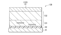
- H—ELECTRICITY
- H10—SEMICONDUCTOR DEVICES; ELECTRIC SOLID-STATE DEVICES NOT OTHERWISE PROVIDED FOR
- H10H—INORGANIC LIGHT-EMITTING SEMICONDUCTOR DEVICES HAVING POTENTIAL BARRIERS
- H10H29/00—Integrated devices, or assemblies of multiple devices, comprising at least one light-emitting semiconductor element covered by group H10H20/00
- H10H29/80—Constructional details
- H10H29/85—Packages
- H10H29/855—Optical field-shaping means, e.g. lenses
- H10H29/8552—Light absorbing arrangements, e.g. black matrix
-
- H—ELECTRICITY
- H10—SEMICONDUCTOR DEVICES; ELECTRIC SOLID-STATE DEVICES NOT OTHERWISE PROVIDED FOR
- H10H—INORGANIC LIGHT-EMITTING SEMICONDUCTOR DEVICES HAVING POTENTIAL BARRIERS
- H10H20/00—Individual inorganic light-emitting semiconductor devices having potential barriers, e.g. light-emitting diodes [LED]
- H10H20/80—Constructional details
- H10H20/85—Packages
- H10H20/855—Optical field-shaping means, e.g. lenses
-
- H—ELECTRICITY
- H10—SEMICONDUCTOR DEVICES; ELECTRIC SOLID-STATE DEVICES NOT OTHERWISE PROVIDED FOR
- H10H—INORGANIC LIGHT-EMITTING SEMICONDUCTOR DEVICES HAVING POTENTIAL BARRIERS
- H10H29/00—Integrated devices, or assemblies of multiple devices, comprising at least one light-emitting semiconductor element covered by group H10H20/00
- H10H29/80—Constructional details
- H10H29/85—Packages
- H10H29/8506—Containers
-
- H—ELECTRICITY
- H10—SEMICONDUCTOR DEVICES; ELECTRIC SOLID-STATE DEVICES NOT OTHERWISE PROVIDED FOR
- H10W—GENERIC PACKAGES, INTERCONNECTIONS, CONNECTORS OR OTHER CONSTRUCTIONAL DETAILS OF DEVICES COVERED BY CLASS H10
- H10W90/00—Package configurations
Definitions
- the present technology relates to a light emitting device and a display device having a light emitting element and a semiconductor element on a substrate.
- Light emitting elements such as a light emitting diode (LED: Light Emitting Diode) are applied to various devices (for example, see Patent Document 1).
- LED Light Emitting Diode
- a plurality of light emitting elements and a plurality of semiconductor elements are provided on a substrate.
- the semiconductor element is, for example, an IC (Integrated Circuit) chip or the like.
- a light-emitting device includes a substrate, a light-emitting element provided on the substrate, and a multi-layer wiring layer and a semiconductor layer provided on the substrate in this order from the substrate side.
- a semiconductor element having a light-shielding portion for suppressing light from entering the element, wherein the light-shielding portion is provided between the first light-shielding surface and the multilayer wiring layer facing the substrate with the semiconductor layer interposed therebetween.
- a second light-shielding surface arranged in a direction intersecting the first light-shielding surface.
- a display device includes the light emitting device according to the embodiment of the present technology.
- the semiconductor element is provided with the light shielding portion that suppresses the incidence of light from the light emitting element, the incidence of light from the light emitting element to the semiconductor element is suppressed.
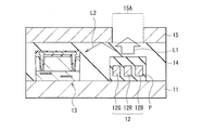
- FIG. 1 is a schematic cross-sectional view illustrating a configuration of a main part of a display device according to a first embodiment of the present technology.
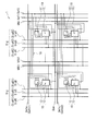
- FIG. 2 is a diagram illustrating an example of an overall circuit configuration of the display device illustrated in FIG. 1.
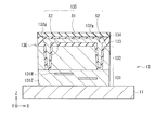
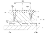
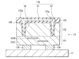
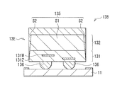
- FIG. 2 is a schematic cross-sectional view illustrating a driving IC illustrated in FIG. 1 in an enlarged manner.
- FIG. 4 is a schematic sectional view illustrating a configuration of a terminal region of the drive IC illustrated in FIG. 3.
- FIG. 4 is a schematic cross-sectional view illustrating a configuration of a bump connecting the drive IC and the substrate illustrated in FIG. 3.
- FIG. 4 is a schematic plan view illustrating a configuration of a first light shielding surface illustrated in FIG. 3.
- FIG. 4 is a schematic plan view illustrating a configuration of a groove illustrated in FIG. 3.
- FIG. 7 is a schematic view illustrating another example (1) of the planar configuration of the groove illustrated in FIG. 6.
- FIG. 7 is a schematic diagram illustrating another example (2) of the planar configuration of the groove illustrated in FIG. 6.
- FIG. 4 is a schematic diagram illustrating another example (1) of the cross-sectional configuration of the groove illustrated in FIG. 3.
- FIG. 4 is a schematic diagram illustrating another example (2) of the cross-sectional configuration of the groove illustrated in FIG. 3.
- FIG. 4 is a schematic diagram illustrating another example (3) of the cross-sectional configuration of the groove illustrated in FIG. 3.
- FIG. 4 is a schematic diagram illustrating another example (1) of a cross-sectional configuration of a light-shielding portion illustrated in FIG.
- FIG. 5 is a schematic diagram illustrating another example (2) of a cross-sectional configuration of the light-shielding portion illustrated in FIG. 3.
- FIG. 4 is a schematic diagram illustrating another example (3) of a cross-sectional configuration of a light-shielding portion illustrated in FIG. 3.
- FIG. 6 is a schematic diagram illustrating another example (4) of a cross-sectional configuration of the light-shielding portion illustrated in FIG. 3.
- FIG. 4 is a schematic cross-sectional view illustrating one process of a method of manufacturing the drive IC illustrated in FIG. 3.
- FIG. 13B is a schematic sectional view illustrating a step following FIG. 13A.
- FIG. 13C is a schematic sectional view illustrating a step following FIG. 13B.
- FIG. 13B is a schematic sectional view illustrating a step following FIG. 13B.
- FIG. 13C is a schematic sectional view illustrating a step following FIG. 13C.
- FIG. 13C is a schematic sectional view illustrating a step following FIG. 13D.
- FIG. 13C is a schematic sectional view illustrating a step following FIG. 13E.
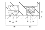
- FIG. 6 is a schematic cross-sectional view illustrating a configuration of a main part of a display device according to a comparative example.
- FIG. 2 is a schematic cross-sectional view illustrating an example of a path of light emitted from the light emitting element illustrated in FIG. 1.
- 13 is a schematic cross-sectional view illustrating a configuration of a drive IC according to Modification Example 1.
- FIG. 13 is a schematic cross-sectional view illustrating a configuration of a drive IC according to Modification Example 2.
- FIG. FIG. 18 is a schematic cross-sectional view illustrating another example of the configuration of the drive IC illustrated in FIG. 17.
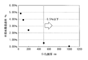
- FIG. 19 is a diagram illustrating a relationship between a thickness of a light shielding portion illustrated in FIG. 18 and a transmittance of light to a semiconductor layer.
- FIG. 18 is a schematic sectional view illustrating one step of a method for manufacturing the drive IC illustrated in FIG. 17 and the like.
- FIG. 21 is a schematic cross-sectional view illustrating another example of the method for manufacturing the drive IC illustrated in FIG. 20.
- FIG. 9 is a schematic cross-sectional view illustrating a configuration of a main part of a display device according to a second embodiment of the present technology.
- FIG. 9 is a schematic cross-sectional view illustrating a configuration of a main part of a display device according to a second embodiment of the present technology.
- FIG. 23 is a schematic sectional view illustrating another example of the display device illustrated in FIG. 22.
- FIG. 23 is a schematic cross-sectional view illustrating one process of a method of manufacturing the display device illustrated in FIG. 22.
- FIG. 25B is a schematic sectional view illustrating a step following FIG. 24A.
- 13 is a schematic cross-sectional view illustrating a configuration of a display device according to Modification Example 3.
- FIG. 14 is a schematic cross-sectional view illustrating a configuration of a display device according to Modification Example 4.
- FIG. FIG. 26 is a schematic sectional view illustrating another example of the display device illustrated in FIG. 25.
- FIG. 27 is a schematic sectional view illustrating another example of the display device illustrated in FIG. 26.
- FIG. 11 is a schematic cross-sectional view illustrating a configuration of a main part of a display device according to a third embodiment of the present technology.
- FIG. 30 is a schematic sectional view illustrating another example of the display device illustrated in FIG. 29.
- FIG. 30 is a schematic diagram illustrating a planar configuration of a groove illustrated in FIG. 29 and the like.
- FIG. 30 is a schematic diagram illustrating another example of the planar configuration of the groove illustrated in FIG. 29 and the like.
- FIG. 30 is a schematic diagram illustrating another example (1) of the cross-sectional configuration of the groove illustrated in FIG. 29 and the like.
- FIG. 30 is a schematic diagram illustrating another example (2) of the cross-sectional configuration of the groove illustrated in FIG. 29 and the like.
- FIG. 30 is a schematic cross-sectional view illustrating an example in which the display device illustrated in FIG. 29 or the like includes an antireflection film.
- FIG. 34B is a schematic sectional view illustrating another example of the configuration of the antireflection film illustrated in FIG. 34A.
- FIG. 30 is a schematic cross-sectional view illustrating one process of a method of manufacturing the display device illustrated in FIG. 29.
- FIG. 35C is a schematic sectional view illustrating a step following FIG. 35A.
- 15 is a schematic cross-sectional view illustrating a configuration of a display device according to Modification Example 5.
- FIG. FIG. 37 is a schematic sectional view illustrating another example of the display device illustrated in FIG. 36.
- FIG. 39 is a schematic sectional view illustrating another example of the display device illustrated in FIG. 38.
- FIG. 39 is a schematic cross-sectional view illustrating one process of a method of manufacturing the display device illustrated in FIG. 38.
- FIG. 40C is a schematic sectional view illustrating a step following FIG. 40A.
- FIG. 40 is a schematic sectional view illustrating another example (1) of the method of manufacturing the display device illustrated in FIGS. 40A and 40B.
- FIG. 39 is a schematic sectional view illustrating another example (2) of the method of manufacturing the display device illustrated in FIG. 38.
- FIG. 42B is a schematic sectional view illustrating a step following FIG. 42A.
- FIG. 39 is a schematic cross-sectional view illustrating another example (3) of the method of manufacturing the display device illustrated in FIG. 38.
- FIG. 43B is a schematic sectional view illustrating a step following FIG. 43A.
- FIG. 15 is a schematic cross-sectional view illustrating a configuration of a main part of a display device according to a fifth embodiment of the present technology.
- FIG. 45 is a schematic sectional view illustrating another example (1) of the display device illustrated in FIG. 44.
- FIG. 45 is a schematic sectional view illustrating another example (2) of the display device illustrated in FIG. 44. It is a cross section showing the composition of the principal section of the display concerning a 6th embodiment of this art.
- FIG. 48 is a schematic sectional view illustrating another example of the display device illustrated in FIG. 47.
- FIG. 48 is a schematic sectional view illustrating another example of the display device illustrated in FIG. 47.
- FIG. 48 is a schematic view illustrating another example of the cross-sectional configuration of the light-blocking member illustrated in FIG. 47 and the like.
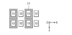
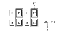
- FIG. 48 is a schematic view illustrating an example of a planar configuration of a light shielding member illustrated in FIG. 47 and the like.
- FIG. 50B is a schematic view illustrating another example (1) of the planar configuration of the light shielding member illustrated in FIG. 50A.
- FIG. 50B is a schematic view illustrating another example (2) of the planar configuration of the light shielding member illustrated in FIG. 50A.
- FIG. 50B is a schematic view illustrating another example (3) of the planar configuration of the light shielding member illustrated in FIG. 50A.
- FIG. 50B is a schematic view illustrating another example (4) of the planar configuration of the light shielding member illustrated in FIG. 50A.
- FIG. 48 is a schematic sectional view illustrating one step of a method of manufacturing the display device illustrated in FIG. 47 and the like.
- FIG. 52B is a schematic sectional view illustrating a step following FIG. 52A.
- FIG. 53 is a schematic sectional view illustrating a step following FIG. 52B.
- FIG. 52C is a schematic sectional view illustrating a step following FIG. 52C.
- FIG. 53D is a schematic sectional view illustrating a step following FIG. 52D.
- FIG. 52 is a schematic cross-sectional view illustrating another example of a method for manufacturing the display device illustrated in FIGS. 52A to 52E.
- FIG. 53B is a schematic sectional view illustrating a step following FIG. 53A.
- FIG. 53B is a schematic sectional view illustrating a step following FIG. 53B.
- First embodiment display device including semiconductor element having light-shielding portion
- Modification 1 an example in which the light-shielding portion has a third light-shielding surface in addition to the first light-shielding surface and the second light-shielding surface
- Modification 2 an example in which the light shielding portion is made of an inorganic insulating material
- Second embodiment display device having a protective layer provided with a thick film portion and a thin film portion
- Modification 3 an example in which the surface of the thin film portion has a lens shape
- Modified example 4 (an example having a dug portion in a thin film portion) 7.
- Third embodiment (display device having light-shielding film embedded in groove of protective layer) 8.
- Modification 5 (an example in which a light-shielding film is embedded in an opening of a protective layer) 9.
- Fourth embodiment (display device having a protective layer provided with a plurality of irregularities on the surface) 10.
- Fifth embodiment (display device having protective layer including low refractive index film and high refractive index film) 11.
- Sixth embodiment (display device having light blocking member between light emitting element and semiconductor element)
- FIG. 1 schematically illustrates a cross-sectional configuration of a main part of a display device (display device 1) according to a first embodiment of the present technology.
- the display device 1 includes, for example, a package 12 and a drive IC 13 on a substrate 11.
- the package 12 includes, for example, three light-emitting elements (light-emitting elements 12R, 12G, and 12B) and a protective body P that covers the light-emitting elements 12R, 12G, and 12B.
- the display device 1 further includes, on the substrate 11, a protective layer 14 covering the package 12 and the driving IC 13, and a light-shielding film 15 on the protective layer 14.
- the light-shielding film 15 has an opening 15 ⁇ / b> A in a region facing the package 12.
- the drive IC 13 is a specific example of a semiconductor element of the present technology
- the display device 1 is a specific example of a light emitting device of the present technology.
- FIG. 2 shows an example of the overall circuit configuration of the display device 1.
- a plurality of pixels 10 are arranged in a matrix.
- Each of the plurality of pixels 10 includes a package 12 and a driving IC 13.
- the display device 1 has, for example, a plurality of signal lines (data lines Sig) extending in the column direction and a plurality of selection lines (gate lines Gate) extending in the row direction, for example.
- the data line Sig and the gate line Gate are formed of, for example, copper.
- the display device 1 further includes a plurality of saw voltage lines Saw, a plurality of power lines VDD1 and VDD2, a plurality of reference voltage lines Ref1 and Ref2, and a plurality of ground lines GND.
- Each saw voltage line Saw extends, for example, in the row direction.
- Each power supply line VDD1, each power supply line VDD2, each reference voltage line Ref1, each reference voltage line Ref2, and each ground line GND extend, for example, in the column direction.
- At least one of the sawtooth voltage line Saw, the power supply lines VDD1 and VDD2, the reference voltage lines Ref1 and Ref2, and the ground line GND may be omitted depending on the driving method.
- the saw voltage line Saw, the power lines VDD1 and VDD2, the reference voltage lines Ref1 and Ref2, and the ground line GND are formed of, for example, copper.
- Each data line Sig is a wiring to which a signal corresponding to a video signal is input by a control circuit (not shown).
- the signal corresponding to the video signal controls, for example, the light emission luminance of the light emitting elements 12R, 12G, and 12B.
- the plurality of data lines Sig include, for example, wiring of a type corresponding to the number of emission colors of the package 12.
- the plurality of data lines Sig include, for example, a plurality of data lines SigR, a plurality of data lines SigG, and a plurality of data lines.
- SigB is a wiring to which a signal corresponding to a video signal is input by a control circuit (not shown).
- the signal corresponding to the video signal controls, for example, the light emission luminance of the light emitting elements 12R, 12G, and 12B.
- the plurality of data lines Sig include, for example, wiring of a type corresponding to the number of emission colors of the package 12.
- Each data line SigR is a wiring to which a signal corresponding to a red video signal is input by a control circuit.
- Each data line SigG is a wiring to which a signal corresponding to a green video signal is input by a control circuit.
- Each data line SigB is a wiring to which a signal corresponding to a blue video signal is input by a control circuit.
- the light emission color of the package 12 is not limited to three colors (R, G, B), but may be four or more colors (R, G, B, W).
- the plurality of data lines Sig include a plurality of data lines SigR, a plurality of data lines SigG, and a plurality of data lines SigB, one data line SigR, one data line SigG, and one data line SigB. Is assigned to each pixel column, for example.
- the set of data lines Sig is assigned to each of a plurality of pixel columns. Further, depending on the driving method, the set of data lines Sig can be replaced with a single data line Sig.
- Each gate line Gate is a wiring to which a signal for selecting the package 12 is input by the control circuit.
- the signal for selecting the package 12 is, for example, a signal that starts sampling a signal input to the data line Sig, causes the sampled signal to be input to the package 12, and causes the package 12 to start emitting light.
- One gate line Gate is allocated, for example, for each pixel row.
- Each saw voltage line Saw is a wiring to which a signal having a saw-like waveform is input by the control circuit, for example.
- the signal having the sawtooth waveform is compared with the sampled signal.For example, the signal having the sawtooth waveform is sampled only while the peak value of the signal having the sawtooth waveform is higher than the peak value of the sampled signal.
- a signal is input to the package 12.
- One saw voltage line Saw is allocated, for example, every two pixel rows.
- Each power supply line VDD2 is a wiring to which a drive current supplied to the package 12 is input by the control circuit.
- One power supply line VDD2 is allocated, for example, for every two pixel columns.
- Each power supply line VDD1, each reference voltage line Ref1, each reference voltage line Ref2, and each ground line GND are wirings to which a fixed voltage is input by the control circuit.
- a ground potential is input to each ground line GND.
- One power supply line VDD1 is allocated, for example, for every two pixel columns.
- One reference voltage line Ref1 is assigned, for example, every two pixel columns.
- One reference voltage line Ref2 is assigned, for example, every two pixel columns.
- One ground line GND is assigned, for example, for every two pixel columns.
- the substrate 11 (FIG. 1) is for mounting a plurality of packages 12 and a plurality of driving ICs 13, and is made of, for example, a glass substrate or a resin substrate.
- the substrate 11 may be constituted by a printed circuit board.
- the substrate 11 may be provided with wiring constituting the above circuit.
- the light emitting elements 12R, 12G, and 12B (FIG. 1) of the package 12 are, for example, light emitting elements that emit light in different wavelength ranges, and include an inorganic semiconductor material.
- the light emitting element 12R is an LED chip that emits light in a red wavelength range
- the light emitting element 12G is an LED chip that emits light in a green wavelength range
- the light emitting element 12B is an LED chip that emits light in a blue wavelength range. It is.
- the light emitting elements 12R, 12G, and 12B include, for example, an n-type semiconductor layer, a p-type semiconductor layer, an n-type electrode, and a p-type electrode.
- the protective body P covering the light emitting elements 12R, 12G, 12B is made of, for example, a resin material.
- the package 12 is electrically connected to the drive IC 13 (FIG. 2).
- One electrode (for example, an n-type electrode) of each of the light emitting elements 12R, 12G, and 12B is electrically connected to the drive IC 13 via, for example, a pad electrode (not shown).
- the other electrode (for example, a p-type electrode) of each of the light emitting elements 12R, 12G, and 12B is electrically connected to a ground line GND via, for example, a pad electrode (not shown).
- the drive IC 13 electrically connected to the package 12 is for controlling light emission of the light emitting elements 12R, 12G, and 12B.
- the drive IC 13 is electrically connected to the package 12, and is also electrically connected to the data line Sig, the power supply line VDD1, and the gate line Gate (FIG. 2).
- the specific configuration of the driving IC 13 will be described later.
- the protective layer 14 is provided, for example, over the entire surface of the substrate 11 so as to cover the plurality of packages 12 and the plurality of drive ICs 13 (FIG. 1).
- the protective layer 14 is for protecting the package 12 and the driving IC 13, and is made of an insulating organic material or an insulating inorganic material.
- the insulating organic material include silicone and the like.
- the insulating inorganic material include silicon oxide (SiO) and silicon nitride (SiN).
- the light-shielding film 15 faces the substrate 11 with the protective layer 14 interposed therebetween.
- This light shielding film 15 is a so-called black mask.
- the opening 15A provided in the light shielding film 15 is for taking out light emitted from each package 12 (light emitting elements 12R, 12G, 12B), and is arranged in a region facing each package 12. .
- the size of the opening 15A is such that light emitted from the light emitting elements 12R, 12G, and 12B can be sufficiently extracted.
- the light shielding film 15 is made of, for example, a resin material containing carbon black, for example.
- the light-shielding film 15 may be made of, for example, a metal material such as titanium (Ti), chromium (Cr), nickel (Ni), tungsten (W), and molybdenum (Mo).
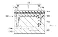
- FIG. 3 is an enlarged view of the driving IC 13 shown in FIG. 1 together with the substrate 11.
- the drive IC 13 has, for example, a multilayer wiring layer 131, a semiconductor layer 132, an inorganic insulating layer 133, and an organic insulating layer 134 in this order from the substrate 11 side.
- the drive IC 13 has a size of, for example, about 200 ⁇ m square.
- the multilayer wiring layer 131 includes, for example, a plurality of wirings 131W and an interlayer insulating film 131Z.
- the plurality of wirings 131W are separated from each other by an interlayer insulating film 131Z.
- the wiring 131W of the multilayer wiring layer 131 is electrically connected to, for example, the data lines SigG, SigR, SigB, and the like.
- the driving IC 13 is electrically connected to the substrate 11 by the multilayer wiring layer 131.
- FIG. 4A and 4B show an example of the configuration of the drive IC 13 electrically connected to the substrate 11.
- the driving IC 13 may be electrically connected to the substrate 11 by the terminal region 131WA of the multilayer wiring layer 131 shown in FIG. 4A. In the terminal region 131WA, for example, a part of the wiring 131W is exposed from the interlayer insulating film 131Z.
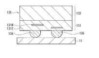
- the driving IC 13 may be electrically connected to the substrate 11 by bumps 136, as shown in FIG. 4B.
- the bump 136 is arranged, for example, between the multilayer wiring layer 131 and the substrate 11.
- the semiconductor layer 132 provided between the multilayer wiring layer 131 and the inorganic insulating layer 133 is made of, for example, silicon (Si).
- the inorganic insulating layer 133 is made of, for example, silicon oxide (SiO), and the organic insulating layer 134 is made of, for example, a resin material.
- the driving IC 13 further has a light shielding unit 135.
- the light-shielding portion 135 is for suppressing light emitted from each of the light-emitting elements 12R, 12G, and 12B from being incident on the drive IC 13. As will be described later in detail, it is possible to suppress occurrence of characteristic fluctuation of the driving IC 13 due to light incident on the driving IC 13 from the light emitting elements 12R, 12G, 12B.
- the light-shielding portion 135 includes, for example, a first light-shielding surface S1 facing the substrate 11 with the semiconductor layer 132 therebetween, and a second light-shielding surface S2 arranged in a direction intersecting the first light-shielding surface S1.
- the second light shielding surface S2 is provided between the first light shielding surface S1 and the multilayer wiring layer 131.
- FIG. 5 shows an example of a plane (XY plane in FIG. 3) configuration of the first light shielding surface S1.
- the first light-shielding surface S1 is provided substantially parallel to the substrate 11 between the semiconductor layer 132 and the organic insulating layer 134, for example.
- the first light-shielding surface S1 is embedded in the inorganic insulating layer 133, and is disposed between the first light-shielding surface S1 and the semiconductor layer 132 and between the first light-shielding surface S1 and the organic insulating layer 134. 133 are provided.
- the first light-shielding surface S1 has, for example, a rectangular planar shape (FIG. 5).
- the first light shielding surface S1 is provided inside the peripheral edge 13E of the driving IC 13.
- the peripheral edge 13E is, for example, a surface exposed by chip separation (separation groove G in FIG. 13F described later) when the drive IC 13 is formed.
- the second light-shielding surface S2 is provided, for example, substantially perpendicular to the first light-shielding surface S1 (FIG. 3).
- the second light-shielding surface S2 is buried in a groove 132g provided from the inorganic insulating layer 133 to the semiconductor layer 132.
- a second light-shielding surface S2 is provided via an inorganic insulating layer 133.
- the groove 132g is provided, for example, from the inorganic insulating layer 133 to the vicinity of the interface between the multilayer wiring layer 131 and the semiconductor layer 132.
- the groove 132g is gradually narrowed, for example, from the inorganic insulating layer 133 toward the multilayer wiring layer 131. That is, the thickness of the light shielding material embedded in the groove 132 g gradually decreases from the inorganic insulating layer 133 toward the multilayer wiring layer 131.
- One end (the upper end in FIG. 3) of the second light shielding surface S2 is in contact with, for example, the first light shielding surface S1, and the other end (the lower end in FIG. 3) is It is preferable to be provided in the vicinity of the interface with. Thereby, the light shielding unit 135 can sufficiently shield the driving IC 13 from light.
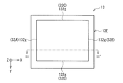
- FIG. 6 shows an example of a plane (XY plane in FIG. 3) configuration of the groove 132g.
- the groove 132g is provided, for example, along the periphery of the first light-shielding surface S1, and has a square planar shape.
- the groove 132g is provided over the entire circumference of the drive IC 13, and is disposed inside the peripheral edge 13E.
- four second light-shielding surfaces S2 (second light-shielding surfaces S2A, S2B, S2C, S2D) are provided in the groove 132g.
- the second light-shielding surfaces S2A, S2B, S2C, S2D are provided over the entire periphery of the drive IC 13.
- the second light-shielding surfaces S2A and S2B are provided substantially parallel to each other.
- the second light-shielding surfaces S2C and S2D are provided between the second light-shielding surface S2A and the second light-shielding surface S2B, and are in contact with the second light-shielding surfaces S2A and S2B.
- the second light-shielding surfaces S2C and S2D are provided substantially parallel to each other. That is, the plurality of second light shielding surfaces S2 (second light shielding surfaces S2A, S2B, S2C, S2D) are in contact with each other. Thereby, since the second light-shielding surfaces S2A, S2B, S2C, S2D are provided without gaps over the entire circumference of the drive IC 13, the drive IC 13 is sufficiently shielded from light.
- FIG. 5 A cross-sectional configuration along the line III-III shown in FIGS. 5 and 6 corresponds to FIG.
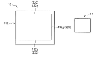
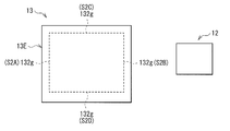
- FIGS. 7 and 8 show another example of the planar configuration of the groove 132g.
- the groove 132g may not be provided over the entire circumference of the driving IC 13.
- a groove 132g may be provided on three sides of the drive IC 13 having a substantially square planar shape, and three second light-shielding surfaces S2 (second light-shielding surfaces S2B, S2C, S2D) may be provided in the groove 132g.
- the second light-shielding surfaces S2B, S2C, S2D (or the groove 132g) be provided at a position facing the package 12 (right side in FIG. 7) around the drive IC 13.
- the second light-shielding surfaces S2B, S2C, S2D can effectively shield light from the package 12 (light-emitting elements 12R, 12G, 12B).
- the groove 132g may not be provided continuously.
- the second light-shielding surfaces S2A, S2B, S2C, S2D may be provided in each of the plurality of grooves 132g separated from each other.
- 9A, 9B, and 9C show another example of the sectional configuration of the groove 132g.
- the groove 132g (the second light-shielding surface S2) may extend from the inorganic insulating layer 133 through the semiconductor layer 132 to reach the multilayer wiring layer 131.
- the groove 132g (the second light-shielding surface S2) may not extend from the inorganic insulating layer 133 to the vicinity of the interface between the semiconductor layer 132 and the multilayer wiring layer 131.
- the second light-shielding surface S2 may be provided along at least a part of the semiconductor layer 132 in the thickness direction.
- the groove 132g may be gradually thicker from the inorganic insulating layer 133 toward the multilayer wiring layer 131. That is, the thickness of the light shielding material embedded in the groove 132g may be gradually increased from the inorganic insulating layer 133 toward the multilayer wiring layer 131.
- the direction of the taper can be changed depending on the forming direction of the groove 132g (described later).
- FIGS. 10, 11, 12A, and 12B show other examples of the cross-sectional configuration of the light-shielding portion 135 (the first light-shielding surface S1 and the second light-shielding surface S2).
- the first light-shielding surface S1 and the second light-shielding surface S2 may be separated from each other, and a gap may be formed therebetween.
- the light-shielding unit 135 can sufficiently shield the drive IC 13 from light.
- sufficient light shielding can be performed.
- the first light-shielding surface S1 may be exposed on the upper surface of the drive IC 13.
- the inorganic insulating layer 133 and the organic insulating layer 134 that cover the first light shielding surface S1 may not be provided.
- the first light-shielding surface S1 may be exposed on the peripheral edge 13E of the drive IC 13.
- the second light-shielding surface S2 may be exposed on the peripheral edge 13E of the drive IC 13.
- the provision of the light-shielding portion 135 (the first light-shielding surface S1 and the second light-shielding surface S2) inside the peripheral edge 13E of the drive IC 13 facilitates the manufacture of the drive IC 13 (described later).
- the light-shielding portion 135 including the first light-shielding surface S1 and the second light-shielding surface S2 shields light in a wavelength band (for example, light in a visible region) emitted from the light-emitting elements 12R, 12G, and 12B. It is made of a material having properties.
- the light shielding portion 135 is made of a metal material such as tungsten (W), titanium (Ti), tantalum (Ta), aluminum (Al), and copper (Cu).
- the light shielding portion 135 may be made of a resin material containing carbon black or the like.
- the drive IC 13 having such a light shielding portion 135 can be manufactured, for example, by the following method (FIGS. 13A to 13F).
- a multilayer wiring layer 131 is formed on a semiconductor layer 132 made of, for example, silicon (Si).
- a groove 132g may be formed in the semiconductor layer 132 from the surface on which the multilayer wiring layer 131 is formed before forming the multilayer wiring layer 131. As a result, a groove 132g (FIG. 9C) that gradually becomes thicker toward the multilayer wiring layer 131 is formed.
- the laminate of the multilayer wiring layer 131 and the semiconductor layer 132 is bonded to the temporary substrate 51 using, for example, an adhesive 52 as shown in FIG. 13B.
- the temporary substrate 51 is made of, for example, a quartz substrate.
- the semiconductor substrate 132 is bonded to the temporary substrate 51 with the multilayer wiring layer 131 interposed therebetween.
- the semiconductor layer 132 is thinned to a desired thickness.
- the inorganic insulating layer 133 and the light shielding portion 135 are formed. Specifically, after a groove 132g is formed in the semiconductor layer 132, for example, silicon oxide (SiO) and tungsten (W) are formed on the entire surface of the semiconductor layer 132 in this order. Thus, silicon oxide and tungsten are formed on the semiconductor layer 132 and buried in the grooves 132g.
- the first light-shielding surface S1 is formed of tungsten formed on the semiconductor layer 132, and the second light-shielding surface S2 is formed of a light-shielding material embedded in the groove 132g.
- An inorganic insulating layer 133 is formed of silicon oxide between the semiconductor layer 132 and the first light-shielding surface S1 and in the groove 132g.
- an inorganic insulating layer 133 covering the first light shielding surface S1 is further formed.
- the first light-shielding surface S1 is etched to a desired size, and an end of the first light-shielding surface S1 is covered with the inorganic insulating layer 133.
- the surface of the inorganic insulating layer 133 is subjected to a flattening process such as CMP (Chemical Mechanical Planarization).
- the multilayer body of the multilayer wiring layer 131, the semiconductor layer 132, and the inorganic insulating layer 133 is inverted, and another temporary substrate ( It is bonded to the temporary substrate 51A).
- the multilayer wiring layer 131 faces the temporary substrate 51A with the inorganic insulating layer 133 and the semiconductor layer 132 therebetween.
- the laminate is bonded to the temporary substrate 51A with, for example, an adhesive 52A.
- chip separation is performed by the separation groove G as shown in FIG. 13F.
- the chip separation is performed using, for example, dry etching.
- the separation groove G is formed, for example, outside the groove 132g.
- the light shielding portion 135 is formed inside the peripheral edge 13E of the drive IC 13 (FIG. 3 and the like).
- a chip material can be easily separated because the metal material or the like constituting the light shielding portion 135 is not etched.
- the first light-shielding surface S1 and the second light-shielding surface S2 may overlap the separation groove G (see FIGS.
- the separation groove G is formed by using laser processing or mechanical processing, the first light shielding surface S1 and the second light shielding surface S2 may overlap the separation groove G.
- a light shielding material in the separation groove G after performing chip separation.
- a light-shielding material such as tungsten (W) is in contact with the temporary substrate 51A. Therefore, when mounting (pickup) the drive IC 13 on the substrate 11, a problem is likely to occur. Therefore, it is preferable to form the light shielding portion 135 before chip separation.
- the drive IC 13 shown in FIG. 3 and the like can be formed in this way.
- the display device for example, when a drive signal is input to each of the light emitting elements 12R, 12G, and 12B via the drive IC 13, light in the red wavelength range is emitted from the light emitting element 12R, and light in the green wavelength range is emitted from the light emitting element 12G. Light and light in the blue wavelength range are emitted from the light emitting element 12B. This light is extracted through the opening 15A of the light shielding film 15. That is, in the display device 1, the light shielding film 15 side is a display surface.
- the drive IC 13 is provided with the light shielding portion 135 for suppressing the incidence of light from the light emitting elements 12R, 12G, and 12B, the light from the light emitting elements 12R, 12G, and 12B to the drive IC 13 is provided. Light incidence is suppressed. Thereby, it is possible to suppress the occurrence of the characteristic fluctuation of the drive IC 13 due to the light incident on the drive IC 13 from the light emitting elements 12R, 12G, 12B.
- this operation and effect will be described.
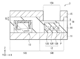
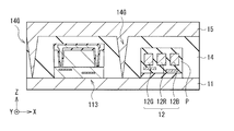
- FIG. 14 illustrates a schematic cross-sectional configuration of a main part of a display device (display device 100) according to a comparative example.
- the display device 100 has a package 12 and a drive IC (drive IC 113) on a substrate 11.
- the drive IC 113 has a multilayer wiring layer 131, a semiconductor layer 132, and an inorganic insulating layer 133 in this order from the substrate 11 side.
- This drive IC 113 does not have a light-shielding portion (light-shielding portion 135 in FIG. 3). In this point, the drive IC 113 of the display device 100 is different from the drive IC 13 of the display device 1.
- the display device 100 has, on a substrate 11, a protective layer 14 that covers the package 12 and the driving IC 113, and a light-shielding film 15 on the protective layer 14.
- An opening 15 ⁇ / b> A is provided in the light shielding film 15 at a position facing the package 12.
- a method of packaging the drive IC 113 with a light-shielding protective body is also conceivable.
- the drive IC 113 of about 200 ⁇ m square is very small.
- the number of drive ICs 113 mounted on the substrate 11 is large. Packaging each of these small drive ICs 113 and mounting a large number of them on the substrate 11 is difficult to mount. Furthermore, this manufacturing process is costly.
- the drive IC 13 since the drive IC 13 has the light blocking portion 135, the incidence of the light L2 from the light emitting elements 12R, 12G, and 12B to the drive IC 13 is suppressed. Thereby, the occurrence of the characteristic fluctuation of the driving IC 13 due to the light L2 is suppressed.
- the drive IC 13 is provided with the light shielding portion 135 for suppressing the incidence of light (light L2) from the light emitting elements 12R, 12G, and 12B. It is possible to suppress occurrence of characteristic fluctuation of the driving IC 13 due to light incident on the IC 13. Therefore, it is possible to suppress a decrease in reliability.
- the light shielding portion 135 has a first light shielding surface S1 facing the substrate 11 with the semiconductor layer 132 therebetween, and a second light shielding surface S2 arranged in a direction intersecting the first light shielding surface S1. .
- the step of chip separation (FIG. 13F) when forming the drive IC 13 is facilitated. Therefore, the drive IC 13 can be easily manufactured.
- the display device 1 may include, instead of the drive IC 13, drive ICs (drive ICs 13A and 13B) according to the following modifications (Modifications 1 and 2).
- FIG. 16 illustrates a schematic cross-sectional configuration of the drive IC 13A according to the first modification.
- the light shielding unit 135 of the driving IC 13A has a third light shielding surface S3 in addition to the first light shielding surface S1 and the second light shielding surface S2.
- the third light-shielding surface S3 is provided on, for example, the multilayer wiring layer 131.
- the third light-shielding surface S3 is opposed to the first light-shielding surface S1 with the second light-shielding surface S2 therebetween, and is in contact with the second light-shielding surface S2.
- the light-shielding portion 135 has the third light-shielding surface S3 in addition to the first light-shielding surface S1 and the second light-shielding surface S2, light from the light emitting elements 12R, 12G, and 12B is more effectively incident on the drive IC 13. Is suppressed.
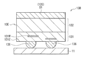
- FIG. 17 illustrates a schematic cross-sectional configuration of a drive IC 13B according to the second modification.
- the light shielding portion 135 of the driving IC 13B is made of an inorganic insulating material such as silicon oxide (SiO).
- the light shielding portion 135 has, for example, a first light shielding surface S1 and a second light shielding surface S2.
- the first light-shielding surface S1 faces the substrate 11 with the semiconductor layer 132 therebetween.
- the first light shielding surface S1 is exposed on the upper surface of the drive IC 13.
- the second light-shielding surface S2 is disposed, for example, between the multilayer wiring layer 131 and the first light-shielding surface S1 substantially perpendicular to the first light-shielding surface S1.
- the second light-shielding surface S2 is exposed, for example, on the peripheral edge 13E of the drive IC 13B.
- the light shielding unit 135 is provided so as to cover the side surface from the upper surface of the driving IC 13B.
- the side surfaces of the multilayer wiring layer 131 and the semiconductor layer 132 may be tapered. This facilitates the formation of the second light-shielding surface S2.
- FIG. 18 shows another example of the driving IC 13B.
- the light shielding unit 135 of the driving IC 13B may be configured by the first light shielding surface S1. In other words, the light shielding unit 135 may not have the second light shielding surface (the second light shielding surface S2 in FIG. 17).
- the inorganic insulating material forming the light shielding unit 135 is, for example, silicon oxide (SiO), silicon nitride (SiN), silicon oxynitride (SiN), SOG (Spin On Glass), or the like.
- the light shield 135 may include a plurality of inorganic insulating materials.
- the thickness of at least the inorganic insulating material forming the first light-shielding surface S1 is preferably 500 nm or more.
- FIG. 19 is a simulation result showing a relationship between the thickness of the silicon oxide forming the first light-shielding surface S1 and the transmittance of light to the semiconductor layer 132.
- This simulation assumes that light is incident on the upper surface of the drive IC 13B at an incident angle of 75 ° to 89 °. From this result, it was found that when the thickness of the inorganic insulating material forming the first light-shielding surface S1 was 500 nm or more, the transmittance of light to the semiconductor layer 132 was reduced to 0.5%.
- FIG. 20 illustrates one step of a method of manufacturing the drive IC 13B.
- an inorganic insulating layer is formed on the semiconductor layer 132 by using a CVD (Chemical Vapor Deposition) method.
- the material is deposited.
- a light shielding portion 135 is formed.
- the driving IC 13B can be formed by the same method as that described in the first embodiment.
- FIG. 21 shows another example of a method of manufacturing the driving IC 13B.
- the light-shielding portion 135 may be formed after the multilayer body of the multilayer wiring layer 131 and the semiconductor layer 132 is mounted on the substrate 11 (after the step of FIG. 21).
- the light shielding portion 135 can be formed by, for example, a sputtering method, an inkjet printing method, a screen printing method, or the like.
- the second light-shielding surface S2 is easily formed in the step of forming the light-shielding portion 135.
- the manufacturing process can be simplified as compared with the driving IC 13 in which the light shielding portion 135 is formed of a metal material or the like.
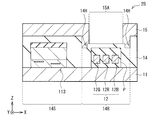
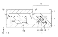
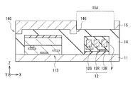
- FIGS. 22 and 23 illustrate a schematic cross-sectional configuration of a main part of a display device (display device 2) according to the second embodiment of the present technology.
- the thickness of the protective layer 14 at the portion facing the drive ICs 13 and 113 is different from the thickness of the protective layer 14 at the portion facing the package 12 (light emitting elements 12R, 12G and 12B).
- the display device 2 may have the drive IC 113 (see FIG. 14) (FIG. 22) or may have the drive IC 13 (see FIG. 1) (FIG. 23). Except for this point, the display device 2 has the same configuration and effects as the display device 1 of the first embodiment.
- the protective layer 14 is provided, for example, over the entire surface of the substrate 11 so as to cover the package 12 and the driving ICs 13 and 113.
- the protective layer 14 has the thick film portion 14S covering the drive ICs 13 and 113 and the periphery thereof, and the thin film portion 14R covering the package 12 and the periphery thereof.
- the thick film portion 14S is provided to face the drive ICs 13 and 113
- the thin film portion 14R is provided to face the package 12 (the light emitting elements 12R, 12G and 12B).
- the thick film portion 14S has a thickness TS on the drive ICs 13 and 113.
- the thin film portion 14R has a thickness TR smaller than the thickness TS on the package 12 (TR ⁇ TS).
- the thickness TS is, for example, 2 ⁇ m to 10 ⁇ m, and the thickness TR is, for example, 0.5 ⁇ m to 3 ⁇ m.
- the light-shielding film 15 faces the substrate 11 with the protective layer 14 interposed therebetween.
- the light-shielding film 15 has an opening 15 ⁇ / b> A at a position facing the package 12.
- the size of the opening 15A in a plan view is smaller than the size of the thin film portion 14R in a plan view.
- the light shielding film 15 is provided so as to cover a part of the thin film portion 14R from the thick film portion 14S. That is, the light shielding film 15 covers the step between the thick film portion 14S and the thin film portion 14R.
- the display device 2 can be manufactured as follows (FIGS. 24A and 24B).
- the protection layer 14 is formed.
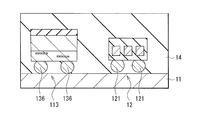
- the package 12 is mounted on the substrate 11 by bumps 121
- the drive IC 113 is mounted on the substrate 11 by bumps 136.
- the protective layer 14 is formed with a substantially uniform thickness over the entire surface of the substrate 11, for example.
- a portion of the protective layer 14 that covers the package 12 and its periphery is selectively etched.
- the thickness of the protective layer 14 covering the package 12 and the periphery thereof is reduced, and the thin film portion 14R and the thick film portion 14S are formed.
- the upper surface of the package 12 may be exposed.
- the light shielding film 15 is formed on the protective layer 14. Thereafter, an opening 15A is formed in the light shielding film 15.
- the display device 2 shown in FIGS. 22 and 23 can be formed in this manner.
- the protective layer 14 since the protective layer 14 has the thin film portion 14R facing the package 12 (the light emitting elements 12R, 12G, and 12B), the light incident on the driving IC 13 from the light emitting elements 12R, 12G, and 12B is reduced. It is possible to suppress the occurrence of the characteristic fluctuation of the driving IC 13 due to the occurrence. Therefore, it is possible to suppress a decrease in reliability.
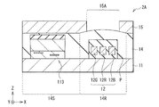
- FIG. 25 illustrates a schematic cross-sectional configuration of a main part of a display device (display device 2A) according to a modified example (modified example 3) of the second embodiment.
- the surface of the thin film portion 14R of the protective layer 14 may have a convex lens shape. This makes it difficult for the light emitted from the light emitting elements 12R, 12G, and 12B to be totally reflected on the surface of the protective layer 14 (the thin film portion 14R). Therefore, light emitted from the light emitting elements 12R, 12G, and 12B and diffused into the protective layer 14 can be further reduced.
- FIG. 26 illustrates a schematic cross-sectional configuration of a main part of a display device (display device 2B) according to a modified example (modified example 4) of the second embodiment.
- the dug portion 14H may be provided in the thin film portion 14R.
- the digging portion 14H is disposed, for example, near the boundary with the thick film portion 14S in the thin film portion 14R. That is, the dug portion 14H is disposed at the edge of the thin film portion 14R. In the dug portion 14H, a part of the thin film portion 14R is dug in a groove shape. It is preferable that the dug portion 14H is provided as deep as possible within a range where the flatness of the light shielding film 15 can be maintained. For example, a light shielding film 15 extending from the thick film portion 14S is embedded in the dug portion 14H.
- reflected light generated in the upper layer of the package 12 is absorbed by the light shielding film 15 embedded in the dug portion 14H.
- the reflected light generated in the upper layer of the package 12 is, for example, light reflected at the interface between the package 12 (protective body P) and the protective layer 14, light reflected on the surface of the protective layer 14, and the like. Therefore, by providing the dug portion 14H, the light emitted from the light emitting elements 12R, 12G, and 12B and diffused into the protective layer 14 can be further reduced.
- the surface of the thin film portion 14R may be formed in a lens shape (FIG. 25), and the dug portion 14H may be provided.
- FIG. 27 shows another example of the display device 2A
- FIG. 28 shows another example of the display device 2B.
- the thickness of the protective layer 14 may be reduced over the entire surface of the substrate 11.
- the surface of the portion of the protective layer 14 facing the package 12 may be formed in a lens shape (FIG. 27), or a dug portion 14H may be provided around the package 12 (FIG. 28).
- Such a protective layer 14 is formed, for example, by forming a constituent material of the protective layer 14 on the entire surface of the substrate 11 and then thinning the film by a method such as etch-back.
- a patterning step for selectively forming a thin film portion is not required. Therefore, the manufacturing process is simplified, and the productivity can be improved.
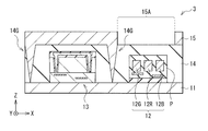
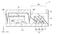
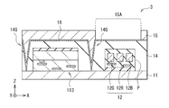
- FIGS. 29 and 30 illustrate a schematic cross-sectional configuration of a main part of a display device (display device 3) according to the third embodiment of the present technology.
- the light-shielding film 15 is embedded in the thickness direction of the protective layer 14 (the Z direction in FIGS. 29 and 30).
- the display device 3 may have the drive IC 113 (see FIG. 14) (FIG. 29) or may have the drive IC 13 (see FIG. 1) (FIG. 30). Except for this point, the display device 3 has the same configuration and effects as the display device 1 of the first embodiment.
- the protective layer 14 has, for example, a groove 14G between the package 12 (the light emitting elements 12R, 12G, and 12B) and the driving ICs 13 and 113.
- the light shielding film 15 is embedded in the groove 14G.
- the light-shielding film 15 is provided continuously from, for example, the protective layer 14 to the bottom of the groove 14G.
- the groove 14 ⁇ / b> G is provided, for example, from the surface of the protective layer 14 to the vicinity of the interface between the protective layer 14 and the substrate 11.
- the cross-sectional shape of the groove 14 ⁇ / b> G gradually decreases from the surface of the protective layer 14 toward the substrate 11. That is, the groove 14G has a wedge-shaped cross-sectional shape.
- FIGS. 31A and 31B show an example of a plane (XY plane in FIGS. 29 and 30) configuration of the groove 14G.
- the groove 14G is provided so as to surround the drive ICs 13 and 113, for example, as shown in FIG. 31A.
- a groove 14G may be provided so as to surround the package 12.
- FIGS. 32 and 33 show other examples of the cross-sectional shape of the groove 14G.
- the groove 14G may not be provided over the entire protective layer 14 in the thickness direction.
- the groove 14G may be provided in a part of the protective layer 14 in the thickness direction.
- the thickness of the groove 14G in the depth direction may be constant.
- the groove 14G has, for example, a rectangular cross-sectional shape.
- the light shielding film 15 is provided between the package 12 (light emitting elements 12R, 12G, 12B) and the driving ICs 13, 113. Therefore, light emitted from the light emitting elements 12R, 12G, and 12B and propagating through the protective layer 14 is absorbed by the light shielding film 15 embedded in the groove 14G. Therefore, the occurrence of the characteristic fluctuation of the driving IC 13 due to the light (the light L2 in FIG. 14) propagating through the protection layer 14 can be suppressed.
- FIGS. 34A and 34B show a cross-sectional configuration of the display device 3 having the light-shielding film 15 and the antireflection film (the antireflection film 16) in the grooves 14G of the protective layer 14.
- FIG. 34A and 34B show a cross-sectional configuration of the display device 3 having the light-shielding film 15 and the antireflection film (the antireflection film 16) in the grooves 14G of the protective layer 14.
- the anti-reflection film 16 is provided, for example, between the protection layer 14 and the light-shielding film 15 and is provided continuously from above the protection layer 14 to the bottom of the groove 14G.
- the antireflection film 16 has, for example, the same planar shape as the light shielding film 15 and has an opening corresponding to the opening 15A of the light shielding film 15 (FIG. 34A).
- the antireflection film 16 may be provided over the entire surface of the substrate 11 (FIG. 34B).
- the antireflection film 16 is made of, for example, a material having a refractive index different from that of the protective layer 14.
- the antireflection film 16 is made of, for example, a silicon oxide film, an ITO (Indium Tin Oxide) film, an IZO (Indium Zinc Oxide) film, a silicon nitride film, or an acrylic transparent resin film.
- the display device 3 can be manufactured as follows (FIGS. 35A and 35B).
- the protective layer 14 is formed (FIG. 24A).
- a groove 14G is formed in the protective layer 14 around the driving IC 113.
- the formation of the groove 14G is performed using, for example, a laser beam LL.
- the groove 14G can be easily formed in a short time.
- the light shielding film 15 is formed so as to fill the groove 14G from above the protective layer 14. Thereafter, an opening 15A is formed in the light shielding film 15.
- the display device 3 shown in FIGS. 29 and 30 can be formed in this manner.
- the light-shielding film 15 is embedded in the groove 14G of the protective layer 14, it is possible to suppress the occurrence of the characteristic fluctuation of the drive IC 13 due to the light incident on the drive IC 13 from the light emitting elements 12R, 12G, 12B. Can be. Therefore, it is possible to suppress a decrease in reliability.
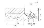
- FIG. 36 illustrates a schematic cross-sectional configuration of a main part of a display device (display device 3A) according to a modification (modification 5) of the third embodiment.
- a light-shielding film 15 is embedded in a region where the protective layer 14 is removed (removed region 14A). As described above, the light shielding film 15 may be embedded in the thickness direction of the protective layer 14.
- the removal region 14A is a region where the protective layer 14 has been removed.
- the removal region 14A is provided in a region facing the driving IC 113 (or the driving IC 13) and its periphery.
- the drive IC 113 is provided in the removal area 14A, and the periphery of the drive IC 113 is covered with the light shielding film 15.
- the light shielding film 15 is in contact with, for example, the upper surface and the side surface of the drive IC 113.
- FIG. 37 shows another example of the display device 3A.
- the entire protective layer 14 may not be removed.
- the protective layer 14 may partially remain in the thickness direction.
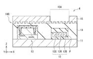
- ⁇ Fourth embodiment> 38 and 39 illustrate a schematic cross-sectional configuration of a main part of a display device (the display device 4) according to the fourth embodiment of the present technology.
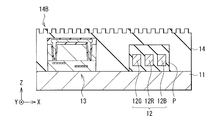
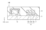
- a plurality of irregularities 14B are provided on the surface of the protective layer 14 (the surface on the side of the light-shielding film 15).
- the display device 4 may have the drive IC 113 (see FIG. 14) (FIG. 39) or may have the drive IC 13 (see FIG. 1) (FIG. 38). Except for this point, the display device 4 has the same configuration and effects as those of the display device 1 of the first embodiment.
- the unevenness 14B provided on the surface of the protective layer 14 is provided, for example, on the entire surface of the protective layer 14.
- the unevenness 14B has, for example, a substantially rectangular cross-sectional shape.
- the unevenness 14B may have, for example, a cross-sectional shape including a curve such as a substantially semicircular shape (see FIG. 43B described later).
- the unevenness 14B is provided at a pitch of, for example, about 200 nm (for example, the size in the X direction and the Y direction in FIGS. 38 and 39), and the height of the unevenness 14B (for example, FIG. 39 (the size in the Z direction in FIG. 39) is about 200 nm.
- a light shielding film 15 is provided so as to cover the irregularities 14B.
- the change in the refractive index on the surface of the protective layer 14 becomes gentle. Thereby, reflection of light emitted from the package 12 (the light emitting elements 12R, 12G, and 12B) on the surface of the protective layer 14 is suppressed. That is, the same effect as the moth-eye structure can be obtained by the plurality of irregularities 14B provided on the surface of the protective layer 14. Therefore, the occurrence of the characteristic fluctuation of the driving IC 13 due to the light (the light L2 in FIG. 14) propagating through the protection layer 14 can be suppressed.
- the display device 4 can be manufactured as follows (FIGS. 40A and 40B).
- the protective layer 14 is formed (FIG. 24A).
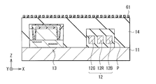
- a resist pattern 61 is formed on the surface of the protective layer.
- the resist pattern 61 is for forming a plurality of irregularities 14B, and corresponds to the shape of the irregularities 14B.
- the resist pattern 61 can be formed, for example, by forming a resist material on the surface of the protective layer 14 and then patterning the resist material into a predetermined shape.
- a plurality of irregularities 14B are formed on the surface of the protective layer 14, as shown in FIG. 40B.
- the plurality of irregularities 14B are formed by, for example, dry etching using the resist pattern 61.
- the resist pattern 61 is removed.
- a light-shielding film 15 is formed on the surface of the protective layer 14.
- an opening 15A is formed in the light shielding film 15.
- the display device 4 shown in FIGS. 38 and 39 can be formed in this manner.
- FIGS. 41 to 43B show another example of a method of forming the plurality of irregularities 14B.
- the surface of the protective layer 14 may be subjected to an ashing process to form a plurality of irregularities 14B.
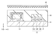
- a plurality of irregularities 14B may be formed by pressing a mold 62 for nanoimprint on the surface of the protective layer 14.
- a square mold 62 may be used (FIGS. 42A and 42B), or a round mold 62 may be used (FIGS. 43A and 43B).
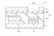
- ⁇ Fifth embodiment> 44 and 45 illustrate a schematic cross-sectional configuration of a main part of a display device (the display device 5) according to the fifth embodiment of the present technology.
- the protective layer 14 of the display device 5 includes a low refractive index film 141 and a high refractive index film 142.
- the display device 5 may have the drive IC 113 (see FIG. 14) (FIG. 45) or may have the drive IC 13 (see FIG. 1) (FIG. 44). Except for this point, the display device 5 has the same configuration and effect as the display device 1 of the first embodiment.
- the low-refractive-index film 141 and the high-refractive-index film 142 are laminated in this order from the substrate 11 side.
- the thickness of the low refractive index film 141 is larger than the thickness of the high refractive index film 142, for example.
- the package 12 and the driving ICs 13 and 113 on the substrate 11 are covered with the low refractive index film 141.
- the low refractive index film 141 is made of, for example, a resin material.
- the refractive index of the low refractive index film 141 is, for example, about 1.5.
- the high refractive index film 142 has a higher refractive index than the low refractive index film 141.
- the high refractive index film 142 is made of, for example, silicon nitride (SiN).
- the refractive index of the high refractive index film 142 is, for example, about 2.0.
- the high refractive index film 142 is provided between the low refractive index film 141 and the light shielding film 15.
- the protective layer 14 has such a laminated structure of the low-refractive-index film 141 and the high-refractive-index film 142, the vicinity of the surface of the protective layer 14 for light emitted from the package 12 (the light emitting elements 12R, 12G, and 12B). Reflection at the surface is suppressed. Therefore, the occurrence of the characteristic fluctuation of the driving IC 13 due to the light (the light L2 in FIG. 14) propagating through the protection layer 14 can be suppressed.
- FIG. 46 shows another example of the display device 5.
- a plurality of minute irregularities 14B may be provided on the surface of the high refractive index film 142. Thereby, reflection near the surface of the protective layer 14 is more effectively suppressed.
- the display device 5 can be manufactured as follows.
- the low refractive index film 141 is formed over the entire surface of the substrate 11.
- a high refractive index film 142 is formed on the low refractive index film 141.
- the protective layer 14 is formed.
- a light-shielding film 15 is formed on the surface of the protective layer 14.
- an opening 15A is formed in the light shielding film 15.
- the display device 5 shown in FIGS. 44 and 45 can be formed in this manner.
- the protective layer 14 since the protective layer 14 has a laminated structure of the low-refractive-index film 141 and the high-refractive-index film 142, the driving IC 13 caused by light incident on the driving IC 13 from the light emitting elements 12R, 12G, and 12B. Can be suppressed from occurring. Therefore, it is possible to suppress a decrease in reliability.
- FIGS. 47 and 48 illustrate a schematic cross-sectional configuration of a main part of a display device (the display device 6) according to the sixth embodiment of the present technology.
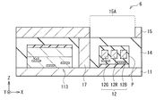
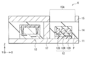
- the display device 6 has a light-shielding member (light-shielding member 17) between the drive ICs 13 and 113 and the package 12.
- the display device 6 may have the drive IC 113 (see FIG. 14) (FIG. 47) or may have the drive IC 13 (see FIG. 1) (FIG. 48). Except for this point, the display device 6 has the same configuration and effect as the display device 1 of the first embodiment.
- the light shielding member 17 extends, for example, in the thickness direction of the protective layer 14, and the lower surface of the light shielding member 17 is in contact with the substrate 11, and the upper surface of the light shielding member 17 is in contact with the light shielding film 15. It is preferable that the light shielding film 15 is provided so as to cover the light shielding member 17.
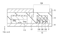
- FIG. 49 shows another example of the cross-sectional configuration of the light blocking member 17.
- the light shielding member 17 does not need to extend over the entire thickness of the protective layer 14, and may extend, for example, to a part of the surface of the protective layer 14.
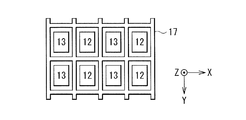
- FIGS. 50A, 50B, and 50C show an example of a plane configuration (XY plane in FIGS. 47 and 48) of the light shielding member 17.
- the light shielding member 17 is provided in a wall shape so as to partition between the drive IC 13 (or the drive IC 113) and the package 12, for example.
- the light blocking members 17 may be provided in a lattice shape.
- the light blocking member 17 may be provided so as to surround either the driving IC 13 or the package 12.
- FIGS. 51A and 51B show another example of the planar configuration of the light shielding member 17.
- the light blocking member 17 may be, for example, columnar.
- a plurality of pillar-shaped light shielding members 17 are provided between the drive IC 13 (or the drive IC 113) and the package 12.
- the light blocking member 17 may be cylindrical.
- the light blocking member 17 may have a prismatic shape.
- the light-blocking member 17 is made of a material having a light-blocking property with respect to light in a wavelength range (for example, light in a visible range) emitted from the light emitting elements 12R, 12G, and 12B.
- the light blocking member 17 is made of a metal material such as tungsten (W), titanium (Ti), tantalum (Ta), aluminum (Al), and copper (Cu).
- the light shielding member 17 may be made of an organic material including carbon black or the like, or may be made of an inorganic material.
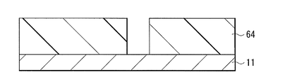
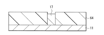
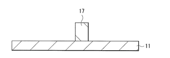
- the display device 6 can be manufactured as follows (FIGS. 52A to 52E).
- the substrate 11 is formed as shown in FIG. 52A.
- a resist pattern 64 is formed on the substrate 11 by using a photolithography method.
- the resist pattern 64 has a pattern corresponding to the light shielding member 17.
- a light-shielding material 17A is formed on the resist pattern 64.
- the unnecessary light shielding material 17A is removed by, for example, etching. Thereby, the light blocking member 17 is formed.
- the resist pattern 64 is removed.
- the drive ICs 13 and 113 and the package 12 are mounted on the substrate 11 on which the light shielding member 17 is provided.
- the protective layer 14 and the light shielding film 15 are formed in this order.
- an opening 15A is formed in the light shielding film 15.
- the display device 6 shown in FIGS. 47 and 48 can be formed in this manner.
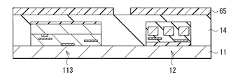
- FIGS. 53A to 53C show another example of the method of manufacturing the display device 6.
- the protective layer 14 is formed (FIG. 24A).
- a resist pattern 65 is formed on the protective layer 14.
- the resist pattern 64 has a pattern corresponding to the light shielding member 17.
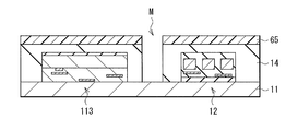
- a groove M is formed in the protective layer 14 using the resist pattern 64.
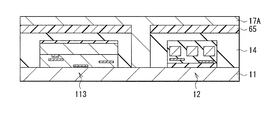
- a light-shielding material 17A is formed from above the resist pattern 65 so as to fill the groove M.
- the unnecessary light shielding material 17A and the resist pattern 65 are removed by, for example, etching. Thereby, the light blocking member 17 is formed.
- the light shielding film 15 is formed so as to cover the light shielding member 17 and the protective layer 14. Thereafter, an opening 15A is formed in the light shielding film 15.
- the display device 6 shown in FIGS. 47 and 48 can be formed by such a method.
- the light shielding member 17 is formed by embedding the light shielding material 17A in the groove M of the protective layer 14, the height of the plurality of light shielding members 17 (for example, the size in the Z direction in FIGS. 47 and 48).
- the planarization of the protective layer 14 and the depth of the groove M are important. Therefore, processing difficulty is high.
- the light shielding member 17 is formed before the package 12 and the driving ICs 13 and 113 are mounted on the substrate 11 (FIGS. 52A to 52E), the height of the light shielding member 17 is easily adjusted, and a plurality of light shielding members are adjusted. It is easy to make the height of the member 17 uniform.
- the light shielding member 17 is provided between the driving ICs 13 and 113 and the package 12 (light emitting elements 12R, 12G and 12B), light incident on the driving IC 13 from the light emitting elements 12R, 12G and 12B. Therefore, it is possible to suppress the occurrence of the characteristic fluctuation of the driving IC 13 caused by the above. Therefore, it is possible to suppress a decrease in reliability.
- the display devices 1, 2, 2A, 2B, 3, 3A, 4, 5, and 6 (hereinafter, abbreviated as the display device 1) described in the first to sixth embodiments and the like include a plurality of substrates 11 May be a display device in which tiles are laid out in a tile shape, a so-called tiling display.
- the display device 1 described in the first to sixth embodiments and the like is input from the outside, such as a television device, a digital camera, a notebook personal computer, a portable terminal device such as a mobile phone, or a video camera.
- the present invention can be applied to an electronic device of any field that displays a video signal or an internally generated video signal as an image or a video.
- the present technology has been described using the drive IC 13 as a specific example of the semiconductor device of the present technology.
- the semiconductor device of the present technology is not limited thereto.
- the package 12 includes three light emitting elements (light emitting elements 12R, 12G, and 12B) has been described.
- the number of light emitting elements included in the package 12 is, for example, one. Or four or more.
- the present technology may be applied to another device such as a lighting device.
- the present technology can also have the following configurations.
- the semiconductor element is provided with the light-shielding portion that suppresses the incidence of light from the light-emitting element. Occurrence can be suppressed. Therefore, it is possible to suppress a decrease in reliability.
- the light shielding unit is A first light-shielding surface facing the substrate with the semiconductor layer interposed;
- a light-emitting device comprising: a second light-shielding surface disposed between the first light-shielding surface and the multilayer wiring layer in a direction crossing the first light-shielding surface.
- the semiconductor layer has a groove
- or (9) which has a light-shielding member provided between the said light emitting element and the said semiconductor element, and which suppresses incidence of light from the said light emitting element to the said semiconductor element.
- Light emitting device (11) Further, a protective layer provided on the substrate and covering the light emitting element and the semiconductor element; The light-emitting device according to any one of (1) to (10), further including a light-shielding film facing the substrate with the protective layer therebetween and having an opening at a position facing the light-emitting element. . (12) The light emitting device according to (11), wherein the light shielding film is embedded in a thickness direction of the protective layer between the light emitting element and the semiconductor element. (13) The light emitting device according to (11), wherein the protective layer includes a thick film portion facing the semiconductor element and a thin film portion facing the light emitting element and having a smaller thickness than the thick film portion.
- the protective layer includes a low refractive index film and a high refractive index film in order from the substrate side.
- the light shielding unit includes a metal material or a resin material.
- the light shielding unit includes an inorganic insulating material.
- the light shielding unit is A first light-shielding surface facing the substrate with the semiconductor layer interposed;
- (22) Board and A light-emitting element provided on the substrate A semiconductor element provided on the substrate, having a multilayer wiring layer and a semiconductor layer in this order from the substrate side; A protective layer provided on the substrate and covering the light emitting element and the semiconductor element; A light-shielding film having an opening at a position facing the substrate with the protective layer therebetween and facing the light-emitting element, The light-emitting device, wherein the light-shielding film is embedded in a thickness direction of the protective layer between the light-emitting element and the semiconductor element.
- (23) Board and A light-emitting element provided on the substrate A semiconductor element provided on the substrate, having a multilayer wiring layer and a semiconductor layer in this order from the substrate side;
- a protective layer provided on the substrate and covering the light emitting element and the semiconductor element;
- a light-shielding film having an opening at a position facing the substrate with the protective layer therebetween and facing the light-emitting element,
- the protective layer includes a thick film portion facing the semiconductor element and a thin film portion facing the light emitting element and having a smaller thickness than the thick film portion.
- (25) Board and A light-emitting element provided on the substrate A semiconductor element provided on the substrate, having a multilayer wiring layer and a semiconductor layer in this order from the substrate side;
- a protective layer provided on the substrate and covering the light emitting element and the semiconductor element;
- a light-shielding film having an opening at a position facing the substrate with the protective layer therebetween and facing the light-emitting element,
- the light emitting device wherein the protective layer includes a low refractive index film and a high refractive index film in order from the substrate side.
Landscapes
- Led Device Packages (AREA)
- Devices For Indicating Variable Information By Combining Individual Elements (AREA)
- Electroluminescent Light Sources (AREA)
- Structures Or Materials For Encapsulating Or Coating Semiconductor Devices Or Solid State Devices (AREA)
- Physics & Mathematics (AREA)
- General Physics & Mathematics (AREA)
- Engineering & Computer Science (AREA)
- Theoretical Computer Science (AREA)
Abstract
Description
1.第1の実施の形態(遮光部を有する半導体素子を含む表示装置)
2.変形例1(遮光部が、第1遮光面および第2遮光面に加えて第3遮光面を有する例)
3.変形例2(遮光部が無機絶縁材料により構成されている例)
4.第2の実施の形態(厚膜部および薄膜部が設けられた保護層を有する表示装置)
5.変形例3(薄膜部の表面がレンズ形状を有する例)
6.変形例4(薄膜部内に掘込部を有する例)
7.第3の実施の形態(保護層の溝に埋設された遮光膜を有する表示装置)
8.変形例5(遮光膜が保護層の開口に埋設されている例)
9.第4の実施の形態(表面に複数の凹凸が設けられた保護層を有する表示装置)
10.第5の実施の形態(低屈折率膜および高屈折率膜を含む保護層を有する表示装置)
11.第6の実施の形態(発光素子と半導体素子との間に遮光部材を有する表示装置)
(表示装置1の全体構成)
図1は、本技術の第1の実施の形態に係る表示装置(表示装置1)の要部の断面構成を模式的に表したものである。この表示装置1は、例えば、基板11上に、パッケージ12および駆動IC13を有している。パッケージ12は、例えば、3つの発光素子(発光素子12R,12G,12B)と、この発光素子12R,12G,12Bを被覆する保護体Pを含んでいる。表示装置1は、更に、基板11上に、パッケージ12および駆動IC13を覆う保護層14と、この保護層14上の遮光膜15とを有している。遮光膜15には、パッケージ12に対向する領域に開口15Aが設けられている。ここでは、駆動IC13が、本技術の半導体素子の一具体例であり、表示装置1が、本技術の発光装置の一具体例である。
以下では、図1および図2を用いて、表示装置1の各部について具体的に説明する。
次に、駆動IC13の具体的な構成について説明する。
このような遮光部135を有する駆動IC13は、例えば、以下のような方法で製造することができる(図13A~図13F)。
表示装置1では、例えば、駆動IC13を介して各々の発光素子12R,12G,12Bに駆動信号が入力されると、発光素子12Rからは赤色波長域の光、発光素子12Gからは緑色波長域の光、発光素子12Bからは青色波長域の光が各々出射される。この光は、遮光膜15の開口15Aを介して取り出される。即ち、表示装置1では、遮光膜15側が、表示面となる。
本実施の形態の表示装置1では、駆動IC13に、発光素子12R,12G,12Bからの光の入射を抑える遮光部135が設けられているので、発光素子12R,12G,12Bから駆動IC13への光の入射が抑えられる。これにより、発光素子12R,12G,12Bから駆動IC13に入射する光に起因した駆動IC13の特性変動の発生を抑えることができる。以下、この作用および効果について説明する。
図16は、変形例1に係る駆動IC13Aの模式的な断面構成を表している。駆動IC13Aの遮光部135は、第1遮光面S1および第2遮光面S2に加えて、第3遮光面S3を有している。
図17は、変形例2に係る駆動IC13Bの模式的な断面構成を表している。駆動IC13Bの遮光部135は、例えば酸化シリコン(SiO)等の無機絶縁材料により構成されている。
図22および図23は、本技術の第2の実施の形態に係る表示装置(表示装置2)の要部の模式的な断面構成を表している。この表示装置2では、駆動IC13,113に対向する部分の保護層14の厚みと、パッケージ12(発光素子12R,12G,12B)に対向する部分の保護層14の厚みとが異なっている。表示装置2は、駆動IC113(図14参照)を有していてもよく(図22)、駆動IC13(図1参照)を有していてもよい(図23)。この点を除き、表示装置2は上記第1の実施の形態の表示装置1と同様の構成および効果を有している。
図25は、上記第2の実施の形態の変形例(変形例3)に係る表示装置(表示装置2A)の要部の模式的な断面構成を表している。このように、保護層14の薄膜部14Rの表面が凸レンズ形状を有していてもよい。これにより、発光素子12R,12G,12Bから出射された光が、保護層14(薄膜部14R)の表面で全反射しにくくなる。したがって、発光素子12R,12G,12Bから出射され、保護層14内に拡散される光を更に、少なくすることができる。
図26は、上記第2の実施の形態の変形例(変形例4)に係る表示装置(表示装置2B)の要部の模式的な断面構成を表している。このように、薄膜部14R内に掘込部14Hが設けられていてもよい。
図29および図30は、本技術の第3の実施の形態に係る表示装置(表示装置3)の要部の模式的な断面構成を表している。この表示装置3では、保護層14の厚み方向(図29,図30のZ方向)に遮光膜15が埋め込まれている。表示装置3は、駆動IC113(図14参照)を有していてもよく(図29)、駆動IC13(図1参照)を有していてもよい(図30)。この点を除き、表示装置3は上記第1の実施の形態の表示装置1と同様の構成および効果を有している。
図36は、上記第3の実施の形態の変形例(変形例5)に係る表示装置(表示装置3A)の要部の模式的な断面構成を表している。この表示装置3Aでは、保護層14の除去領域(除去領域14A)に遮光膜15が埋め込まれている。このように、遮光膜15を保護層14の厚み方向に埋め込むようにしてもよい。
図38および図39は、本技術の第4の実施の形態に係る表示装置(表示装置4)の要部の模式的な断面構成を表している。この表示装置4では、保護層14の表面(遮光膜15側の面)に複数の凹凸14Bが設けられている。表示装置4は、駆動IC113(図14参照)を有していてもよく(図39)、駆動IC13(図1参照)を有していてもよい(図38)。この点を除き、表示装置4は上記第1の実施の形態の表示装置1と同様の構成および効果を有している。
図44および図45は、本技術の第5の実施の形態に係る表示装置(表示装置5)の要部の模式的な断面構成を表している。この表示装置5の保護層14は、低屈折率膜141および高屈折率膜142を含んでいる。表示装置5は、駆動IC113(図14参照)を有していてもよく(図45)、駆動IC13(図1参照)を有していてもよい(図44)。この点を除き、表示装置5は上記第1の実施の形態の表示装置1と同様の構成および効果を有している。
図47および図48は、本技術の第6の実施の形態に係る表示装置(表示装置6)の要部の模式的な断面構成を表している。この表示装置6は、駆動IC13,113とパッケージ12との間に遮光部材(遮光部材17)を有している。表示装置6は、駆動IC113(図14参照)を有していてもよく(図47)、駆動IC13(図1参照)を有していてもよい(図48)。この点を除き、表示装置6は上記第1の実施の形態の表示装置1と同様の構成および効果を有している。
上記第1~第6の実施の形態等において説明した表示装置1は、例えば、テレビジョン装置,デジタルカメラ,ノート型パーソナルコンピュータ、携帯電話等の携帯端末装置あるいはビデオカメラなど、外部から入力された映像信号あるいは内部で生成した映像信号を、画像あるいは映像として表示するあらゆる分野の電子機器に適用することが可能である。
(1)
基板と、
前記基板上に設けられた発光素子と、
前記基板上に設けられ、前記基板側から多層配線層および半導体層をこの順に有し、かつ、前記発光素子からの光の入射を抑える遮光部を有する半導体素子とを備え、
前記遮光部は、
前記半導体層を間にして前記基板に対向する第1遮光面と、
前記第1遮光面と前記多層配線層との間に、前記第1遮光面に交差する方向に配置された第2遮光面とを含む
発光装置。
(2)
前記遮光部は、前記半導体素子の周縁よりも内側に設けられている
前記(1)に記載の発光装置。
(3)
前記第2遮光面は、前記半導体素子のうち、少なくとも前記発光素子に臨む位置に設けられている
前記(1)または(2)に記載の発光装置。
(4)
前記第2遮光面は、前記半導体素子の全周にわたって設けられている
前記(1)ないし(3)のうちいずれか1つに記載の発光装置。
(5)
複数の前記第2遮光面を有する
前記(1)ないし(4)のうちいずれか1つに記載の発光装置。
(6)
複数の前記第2遮光面は、互いに接して配置されている
前記(5)に記載の発光装置。
(7)
前記半導体層は溝を有し、
前記溝内に、前記第2遮光面が配置されている
前記(1)ないし(6)のうちいずれか1つに記載の発光装置。
(8)
前記第2遮光面は前記第1遮光面に接している
前記(1)ないし(7)のうちいずれか1つに記載の発光装置。
(9)
前記遮光部は、更に、前記第2遮光面を間にして前記第1遮光面に対向する第3遮光面を有する
前記(1)ないし(8)のうちいずれか1つに記載の発光装置。
(10)
更に、前記発光素子と前記半導体素子との間に設けられ、前記発光素子から前記半導体素子への光の入射を抑える遮光部材を有する
前記(1)ないし(9)のうちいずれか1つに記載の発光装置。
(11)
更に、前記基板上に設けられ、前記発光素子および前記半導体素子を覆う保護層と、
前記保護層を間にして前記基板に対向し、かつ、前記発光素子に対向する位置に開口を有する遮光膜とを有する
前記(1)ないし(10)のうちいずれか1つに記載の発光装置。
(12)
前記遮光膜は、前記発光素子と前記半導体素子との間の前記保護層の厚み方向に埋設されている
前記(11)に記載の発光装置。
(13)
前記保護層は、前記半導体素子に対向する厚膜部と、前記発光素子に対向するとともに、前記厚膜部よりも厚みの小さい薄膜部とを有する
前記(11)に記載の発光装置。
(14)
前記遮光膜は、前記薄膜部と前記厚膜部との間の段差を覆っている
前記(13)に記載の発光装置。
(15)
前記保護層の表面には、複数の凹凸が設けられている
前記(11)ないし(14)のうちいずれか1つに記載の発光装置。
(16)
前記保護層は、前記基板側から順に、低屈折率膜および高屈折率膜を含む
前記(11)ないし(15)のうちいずれか1つに記載の発光装置。
(17)
前記遮光部は、金属材料または樹脂材料を含む
前記(1)ないし(16)のうちいずれか1つに記載の発光装置。
(18)
前記遮光部は、無機絶縁材料を含む
前記(1)ないし(17)のうちいずれか1つに記載の発光装置。
(19)
前記遮光部の少なくとも一部は、厚み500nm以上を有する
前記(18)に記載の発光装置。
(20)
発光装置を備え、
前記発光装置は、
基板と、
前記基板上に設けられた発光素子と、
前記基板上に設けられ、前記基板側から多層配線層および半導体層をこの順に有し、かつ、前記発光素子からの光の入射を抑える遮光部を有する半導体素子とを備え、
前記遮光部は、
前記半導体層を間にして前記基板に対向する第1遮光面と、
前記第1遮光面と前記多層配線層との間に、前記第1遮光面に交差する方向に配置された第2遮光面とを含む
表示装置。
(21)
基板と、
前記基板上に設けられた発光素子と、
前記基板上に設けられ、前記基板側から多層配線層および半導体層をこの順に有する半導体素子と、
前記発光素子と前記半導体素子との間に設けられ、前記発光素子から前記半導体素子への光の入射を抑える遮光部材と
を備えた発光装置。
(22)
基板と、
前記基板上に設けられた発光素子と、
前記基板上に設けられ、前記基板側から多層配線層および半導体層をこの順に有する半導体素子と、
前記基板上に設けられ、前記発光素子および前記半導体素子を覆う保護層と、
前記保護層を間にして前記基板に対向し、かつ、前記発光素子に対向する位置に開口を有する遮光膜とを備え、
前記遮光膜は、前記発光素子と前記半導体素子との間の前記保護層の厚み方向に埋設されている
発光装置。
(23)
基板と、
前記基板上に設けられた発光素子と、
前記基板上に設けられ、前記基板側から多層配線層および半導体層をこの順に有する半導体素子と、
前記基板上に設けられ、前記発光素子および前記半導体素子を覆う保護層と、
前記保護層を間にして前記基板に対向し、かつ、前記発光素子に対向する位置に開口を有する遮光膜とを備え、
前記保護層は、前記半導体素子に対向する厚膜部と、前記発光素子に対向するとともに、前記厚膜部よりも厚みの小さい薄膜部とを有する
発光装置。
(24)
基板と、
前記基板上に設けられた発光素子と、
前記基板上に設けられ、前記基板側から多層配線層および半導体層をこの順に有する半導体素子と、
前記基板上に設けられ、前記発光素子および前記半導体素子を覆う保護層と、
前記保護層を間にして前記基板に対向し、かつ、前記発光素子に対向する位置に開口を有する遮光膜とを備え、
前記保護層の表面には、複数の凹凸が設けられている
発光装置。
(25)
基板と、
前記基板上に設けられた発光素子と、
前記基板上に設けられ、前記基板側から多層配線層および半導体層をこの順に有する半導体素子と、
前記基板上に設けられ、前記発光素子および前記半導体素子を覆う保護層と、
前記保護層を間にして前記基板に対向し、かつ、前記発光素子に対向する位置に開口を有する遮光膜とを備え、
前記保護層は、前記基板側から順に、低屈折率膜および高屈折率膜を含む
発光装置。
Claims (20)
- 基板と、
前記基板上に設けられた発光素子と、
前記基板上に設けられ、前記基板側から多層配線層および半導体層をこの順に有し、かつ、前記発光素子からの光の入射を抑える遮光部を有する半導体素子とを備え、
前記遮光部は、
前記半導体層を間にして前記基板に対向する第1遮光面と、
前記第1遮光面と前記多層配線層との間に、前記第1遮光面に交差する方向に配置された第2遮光面とを含む
発光装置。 - 前記遮光部は、前記半導体素子の周縁よりも内側に設けられている
請求項1に記載の発光装置。 - 前記第2遮光面は、前記半導体素子のうち、少なくとも前記発光素子に臨む位置に設けられている
請求項1に記載の発光装置。 - 前記第2遮光面は、前記半導体素子の全周にわたって設けられている
請求項1に記載の発光装置。 - 複数の前記第2遮光面を有する
請求項1に記載の発光装置。 - 複数の前記第2遮光面は、互いに接して配置されている
請求項5に記載の発光装置。 - 前記半導体層は溝を有し、
前記溝内に、前記第2遮光面が配置されている
請求項1に記載の発光装置。 - 前記第2遮光面は前記第1遮光面に接している
請求項1に記載の発光装置。 - 前記遮光部は、更に、前記第2遮光面を間にして前記第1遮光面に対向する第3遮光面を有する
請求項1に記載の発光装置。 - 更に、前記発光素子と前記半導体素子との間に設けられ、前記発光素子から前記半導体素子への光の入射を抑える遮光部材を有する
請求項1に記載の発光装置。 - 更に、前記基板上に設けられ、前記発光素子および前記半導体素子を覆う保護層と、
前記保護層を間にして前記基板に対向し、かつ、前記発光素子に対向する位置に開口を有する遮光膜とを有する
請求項1に記載の発光装置。 - 前記遮光膜は、前記発光素子と前記半導体素子との間の前記保護層の厚み方向に埋設されている
請求項11に記載の発光装置。 - 前記保護層は、前記半導体素子に対向する厚膜部と、前記発光素子に対向するとともに、前記厚膜部よりも厚みの小さい薄膜部とを有する
請求項11に記載の発光装置。 - 前記遮光膜は、前記薄膜部と前記厚膜部との間の段差を覆っている
請求項13に記載の発光装置。 - 前記保護層の表面には、複数の凹凸が設けられている
請求項11に記載の発光装置。 - 前記保護層は、前記基板側から順に、低屈折率膜および高屈折率膜を含む
請求項11に記載の発光装置。 - 前記遮光部は、金属材料または樹脂材料を含む
請求項1に記載の発光装置。 - 前記遮光部は、無機絶縁材料を含む
請求項1に記載の発光装置。 - 前記遮光部の少なくとも一部は、厚み500nm以上を有する
請求項18に記載の発光装置。 - 発光装置を備え、
前記発光装置は、
基板と、
前記基板上に設けられた発光素子と、
前記基板上に設けられ、前記基板側から多層配線層および半導体層をこの順に有し、かつ、前記発光素子からの光の入射を抑える遮光部を有する半導体素子とを備え、
前記遮光部は、
前記半導体層を間にして前記基板に対向する第1遮光面と、
前記第1遮光面と前記多層配線層との間に、前記第1遮光面に交差する方向に配置された第2遮光面とを含む
表示装置。
Priority Applications (3)
| Application Number | Priority Date | Filing Date | Title |
|---|---|---|---|
| JP2020539364A JP7420725B2 (ja) | 2018-08-31 | 2019-08-19 | 発光装置および表示装置 |
| DE112019004314.5T DE112019004314T5 (de) | 2018-08-31 | 2019-08-19 | Lichtemittierende einheit und anzeigevorrichtung |
| KR1020217004698A KR20210049795A (ko) | 2018-08-31 | 2019-08-19 | 발광 장치 및 표시 장치 |
Applications Claiming Priority (2)
| Application Number | Priority Date | Filing Date | Title |
|---|---|---|---|
| JP2018-163023 | 2018-08-31 | ||
| JP2018163023 | 2018-08-31 |
Publications (1)
| Publication Number | Publication Date |
|---|---|
| WO2020045147A1 true WO2020045147A1 (ja) | 2020-03-05 |
Family
ID=69643890
Family Applications (1)
| Application Number | Title | Priority Date | Filing Date |
|---|---|---|---|
| PCT/JP2019/032280 Ceased WO2020045147A1 (ja) | 2018-08-31 | 2019-08-19 | 発光装置および表示装置 |
Country Status (4)
| Country | Link |
|---|---|
| JP (1) | JP7420725B2 (ja) |
| KR (1) | KR20210049795A (ja) |
| DE (1) | DE112019004314T5 (ja) |
| WO (1) | WO2020045147A1 (ja) |
Cited By (3)
| Publication number | Priority date | Publication date | Assignee | Title |
|---|---|---|---|---|
| JPWO2023063085A1 (ja) * | 2021-10-14 | 2023-04-20 | ||
| JP2023522881A (ja) * | 2020-04-16 | 2023-06-01 | テキサス インスツルメンツ インコーポレイテッド | 放射遮蔽を用いる統合されたシステムインパッケージ |
| JP2023179115A (ja) * | 2022-06-07 | 2023-12-19 | 株式会社ジャパンディスプレイ | 表示装置 |
Citations (5)
| Publication number | Priority date | Publication date | Assignee | Title |
|---|---|---|---|---|
| US5990802A (en) * | 1998-05-18 | 1999-11-23 | Smartlite Communications, Inc. | Modular LED messaging sign panel and display system |
| JP2012078720A (ja) * | 2010-10-05 | 2012-04-19 | Sony Corp | 表示パネル、表示装置、照明パネルおよび照明装置、ならびに表示パネルおよび照明パネルの製造方法 |
| JP2012108407A (ja) * | 2010-11-19 | 2012-06-07 | Seiko Epson Corp | 電気光学装置、電気光学装置の製造方法、電子機器 |
| JP2017161634A (ja) * | 2016-03-08 | 2017-09-14 | ソニー株式会社 | 表示体デバイスおよび表示装置 |
| JP2018058738A (ja) * | 2016-10-07 | 2018-04-12 | 旭硝子株式会社 | 表示装置用カバーガラスおよび電子機器 |
Family Cites Families (1)
| Publication number | Priority date | Publication date | Assignee | Title |
|---|---|---|---|---|
| WO2013190871A1 (ja) | 2012-06-20 | 2013-12-27 | アオイ電子株式会社 | 光源一体型光センサ |
-
2019
- 2019-08-19 WO PCT/JP2019/032280 patent/WO2020045147A1/ja not_active Ceased
- 2019-08-19 KR KR1020217004698A patent/KR20210049795A/ko active Pending
- 2019-08-19 DE DE112019004314.5T patent/DE112019004314T5/de not_active Withdrawn
- 2019-08-19 JP JP2020539364A patent/JP7420725B2/ja active Active
Patent Citations (5)
| Publication number | Priority date | Publication date | Assignee | Title |
|---|---|---|---|---|
| US5990802A (en) * | 1998-05-18 | 1999-11-23 | Smartlite Communications, Inc. | Modular LED messaging sign panel and display system |
| JP2012078720A (ja) * | 2010-10-05 | 2012-04-19 | Sony Corp | 表示パネル、表示装置、照明パネルおよび照明装置、ならびに表示パネルおよび照明パネルの製造方法 |
| JP2012108407A (ja) * | 2010-11-19 | 2012-06-07 | Seiko Epson Corp | 電気光学装置、電気光学装置の製造方法、電子機器 |
| JP2017161634A (ja) * | 2016-03-08 | 2017-09-14 | ソニー株式会社 | 表示体デバイスおよび表示装置 |
| JP2018058738A (ja) * | 2016-10-07 | 2018-04-12 | 旭硝子株式会社 | 表示装置用カバーガラスおよび電子機器 |
Cited By (4)
| Publication number | Priority date | Publication date | Assignee | Title |
|---|---|---|---|---|
| JP2023522881A (ja) * | 2020-04-16 | 2023-06-01 | テキサス インスツルメンツ インコーポレイテッド | 放射遮蔽を用いる統合されたシステムインパッケージ |
| JPWO2023063085A1 (ja) * | 2021-10-14 | 2023-04-20 | ||
| JP7671858B2 (ja) | 2021-10-14 | 2025-05-02 | 株式会社ジャパンディスプレイ | 表示装置 |
| JP2023179115A (ja) * | 2022-06-07 | 2023-12-19 | 株式会社ジャパンディスプレイ | 表示装置 |
Also Published As
| Publication number | Publication date |
|---|---|
| DE112019004314T5 (de) | 2021-05-27 |
| JPWO2020045147A1 (ja) | 2021-09-02 |
| KR20210049795A (ko) | 2021-05-06 |
| JP7420725B2 (ja) | 2024-01-23 |
Similar Documents
| Publication | Publication Date | Title |
|---|---|---|
| JP6639462B2 (ja) | 発光ダイオードチップ及びこれを含む発光ダイオードディスプレイ装置 | |
| CN112542437B (zh) | 显示装置 | |
| KR102408164B1 (ko) | 표시 장치 및 그의 제조방법 | |
| CN108231834B (zh) | 发光显示装置及其制造方法 | |
| CN107785393B (zh) | 显示装置及其制造方法 | |
| KR102356841B1 (ko) | 유기 발광 표시 장치 및 그 제조 방법 | |
| US20230284513A1 (en) | Display device, method of manufacturing display device, and electronic apparatus using display device | |
| KR102890701B1 (ko) | 표시 장치 | |
| CN113764477A (zh) | 显示装置 | |
| JP7420725B2 (ja) | 発光装置および表示装置 | |
| CN115904115A (zh) | 触摸检测器件、包括其的显示装置和制造其的方法 | |
| US20240292651A1 (en) | Display device, method of manufacturing display device, electronic apparatus, and lighting device | |
| CN116367591A (zh) | 显示装置 | |
| CN114597241A (zh) | 显示设备和制造显示设备的方法 | |
| CN112771674B (zh) | 电子装置基板及其制作方法、电子装置 | |
| KR102398001B1 (ko) | 유기 발광 표시 장치 | |
| KR20230033058A (ko) | 표시 장치 및 표시 장치의 제조 방법 | |
| US20230363211A1 (en) | Display device including a pad structure sharing material with bank structure | |
| KR20250112345A (ko) | 표시 장치 및 이의 제조 방법 | |
| CN118571880A (zh) | 显示装置 | |
| KR102900409B1 (ko) | 표시 장치 | |
| KR20230132671A (ko) | 표시패널의 제조방법 | |
| US20250008814A1 (en) | Display device including a fluidized layer | |
| US20240237465A9 (en) | Display device including a color filter disposed on a bank structure | |
| KR20250042914A (ko) | 표시 장치 및 이의 제조 방법 |
Legal Events
| Date | Code | Title | Description |
|---|---|---|---|
| 121 | Ep: the epo has been informed by wipo that ep was designated in this application |
Ref document number: 19853848 Country of ref document: EP Kind code of ref document: A1 |
|
| ENP | Entry into the national phase |
Ref document number: 20217004698 Country of ref document: KR Kind code of ref document: A |
|
| ENP | Entry into the national phase |
Ref document number: 2020539364 Country of ref document: JP Kind code of ref document: A |
|
| 122 | Ep: pct application non-entry in european phase |
Ref document number: 19853848 Country of ref document: EP Kind code of ref document: A1 |